Embed Size (px)
Citation preview
1VLSI Design Lab.
AVR Training Board
Konkuk Univ. VLSI Design Lab.
2VLSI Design Lab.
What is microcontroller
A microcontroller is a small, low‐cost computer‐on‐a‐chip which usually includes:
An 8 or 16 bit microprocessor (CPU).A small amount of RAM.Programmable ROM and/or flash memory.Parallel and/or serial I/O.Timers and signal generators.Analog to Digital (A/D) and/or Digital to Analog (D/A) conversion.
3VLSI Design Lab.
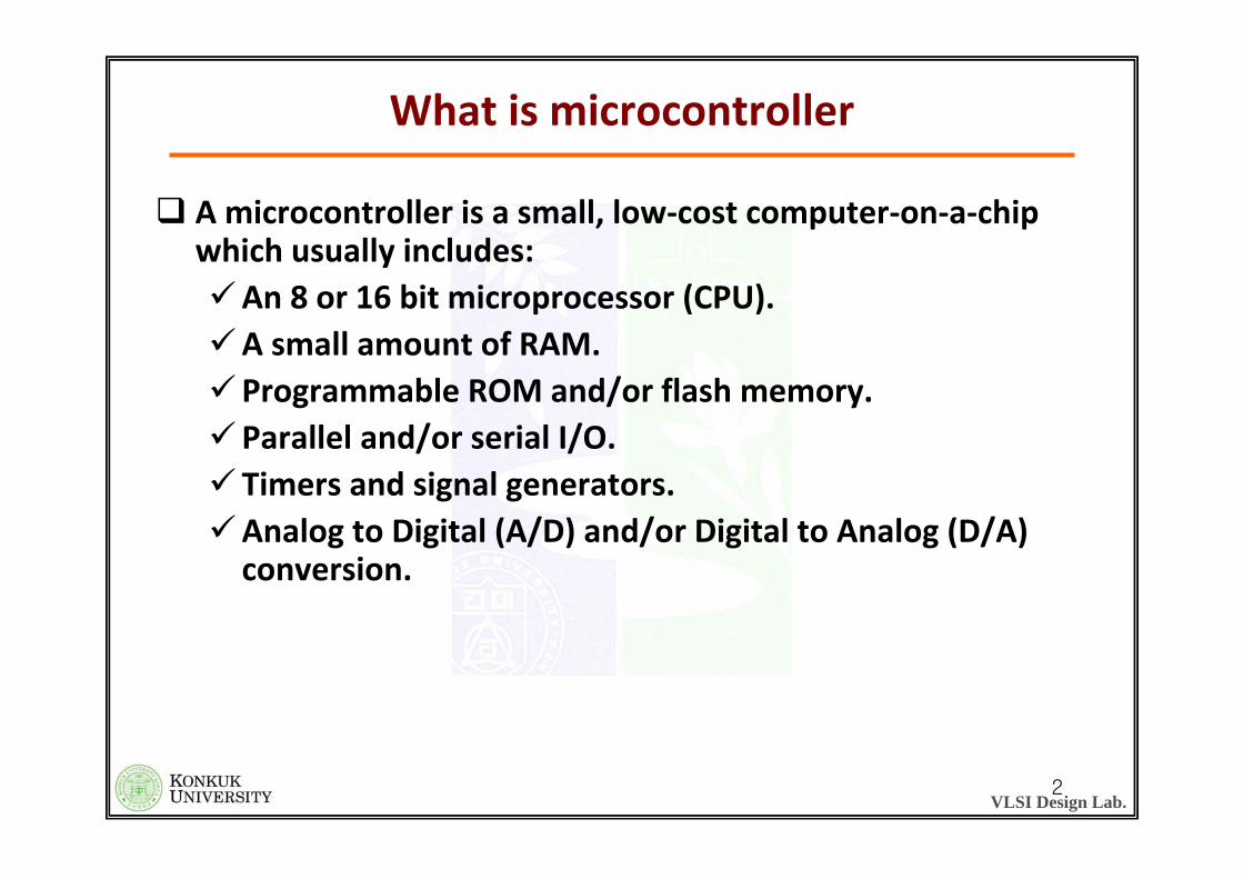
Basics of microcontroller
Examples:Motorola’s 68HC11, 68HC12, AMD 29K, Zilog’s Z8, Z80, Intel’s 8052, Microchip’s PIC Low-power,
embedded versions of desktop CPUs: e.g Intel’s 80486
4VLSI Design Lab.
Microcontrollers
Intel 8051 ARM Atmel AVR 8/32‐bit architectureFreescale CF (32‐bit), Freescale S08(8‐bit) , 68HC11(8‐bit)Hitachi H8, Hitachi SuperHMIPS (32‐bit PIC32) NEC V850 PIC (8‐bit PIC16, PIC18, 16‐bit dsPIC33 / PIC24) PowerPC ISE PSoC (Programmable System‐on‐Chip) Rabbit 2000 TI MSP430 (16‐bit) Toshiba TLCS‐870 Zilog eZ8, eZ80…
5VLSI Design Lab.
Atmel AVR Microcontroller
The AVR is a Modified Harvard architecture 8‐bit RISC single chip microcontroller which was developed by Atmel in 1996.The AVR was one of the first microcontroller families to use on‐chip flash memory for program storage, as opposed to One‐Time Programmable ROM, EPROM, or EEPROM used by other microcontrollers at the time.Families of AVR
tinyAVR — the ATtiny seriesmegaAVR — the ATmega seriesXMEGA — the ATxmega seriesApplication specific AVR
6VLSI Design Lab.
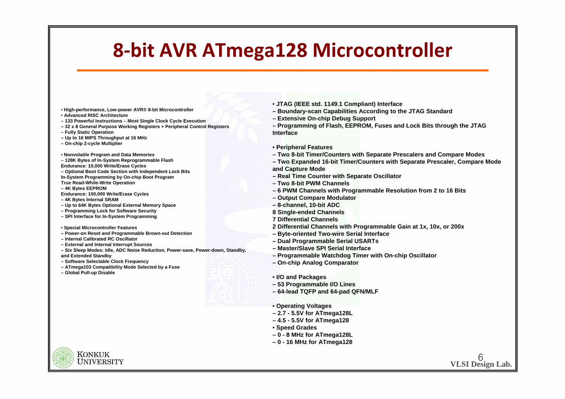
8‐bit AVR ATmega128 Microcontroller
• High-performance, Low-power AVR® 8-bit Microcontroller• Advanced RISC Architecture– 133 Powerful Instructions – Most Single Clock Cycle Execution– 32 x 8 General Purpose Working Registers + Peripheral Control Registers– Fully Static Operation– Up to 16 MIPS Throughput at 16 MHz– On-chip 2-cycle Multiplier
• Nonvolatile Program and Data Memories– 128K Bytes of In-System Reprogrammable FlashEndurance: 10,000 Write/Erase Cycles– Optional Boot Code Section with Independent Lock BitsIn-System Programming by On-chip Boot ProgramTrue Read-While-Write Operation– 4K Bytes EEPROMEndurance: 100,000 Write/Erase Cycles– 4K Bytes Internal SRAM– Up to 64K Bytes Optional External Memory Space– Programming Lock for Software Security– SPI Interface for In-System Programming
• Special Microcontroller Features– Power-on Reset and Programmable Brown-out Detection– Internal Calibrated RC Oscillator– External and Internal Interrupt Sources– Six Sleep Modes: Idle, ADC Noise Reduction, Power-save, Power-down, Standby,and Extended Standby– Software Selectable Clock Frequency– ATmega103 Compatibility Mode Selected by a Fuse– Global Pull-up Disable
• JTAG (IEEE std. 1149.1 Compliant) Interface– Boundary-scan Capabilities According to the JTAG Standard– Extensive On-chip Debug Support– Programming of Flash, EEPROM, Fuses and Lock Bits through the JTAG Interface
• Peripheral Features– Two 8-bit Timer/Counters with Separate Prescalers and Compare Modes– Two Expanded 16-bit Timer/Counters with Separate Prescaler, Compare Mode and Capture Mode– Real Time Counter with Separate Oscillator– Two 8-bit PWM Channels– 6 PWM Channels with Programmable Resolution from 2 to 16 Bits– Output Compare Modulator– 8-channel, 10-bit ADC8 Single-ended Channels7 Differential Channels2 Differential Channels with Programmable Gain at 1x, 10x, or 200x– Byte-oriented Two-wire Serial Interface– Dual Programmable Serial USARTs– Master/Slave SPI Serial Interface– Programmable Watchdog Timer with On-chip Oscillator– On-chip Analog Comparator
• I/O and Packages– 53 Programmable I/O Lines– 64-lead TQFP and 64-pad QFN/MLF
• Operating Voltages– 2.7 - 5.5V for ATmega128L– 4.5 - 5.5V for ATmega128• Speed Grades– 0 - 8 MHz for ATmega128L– 0 - 16 MHz for ATmega128
7VLSI Design Lab.
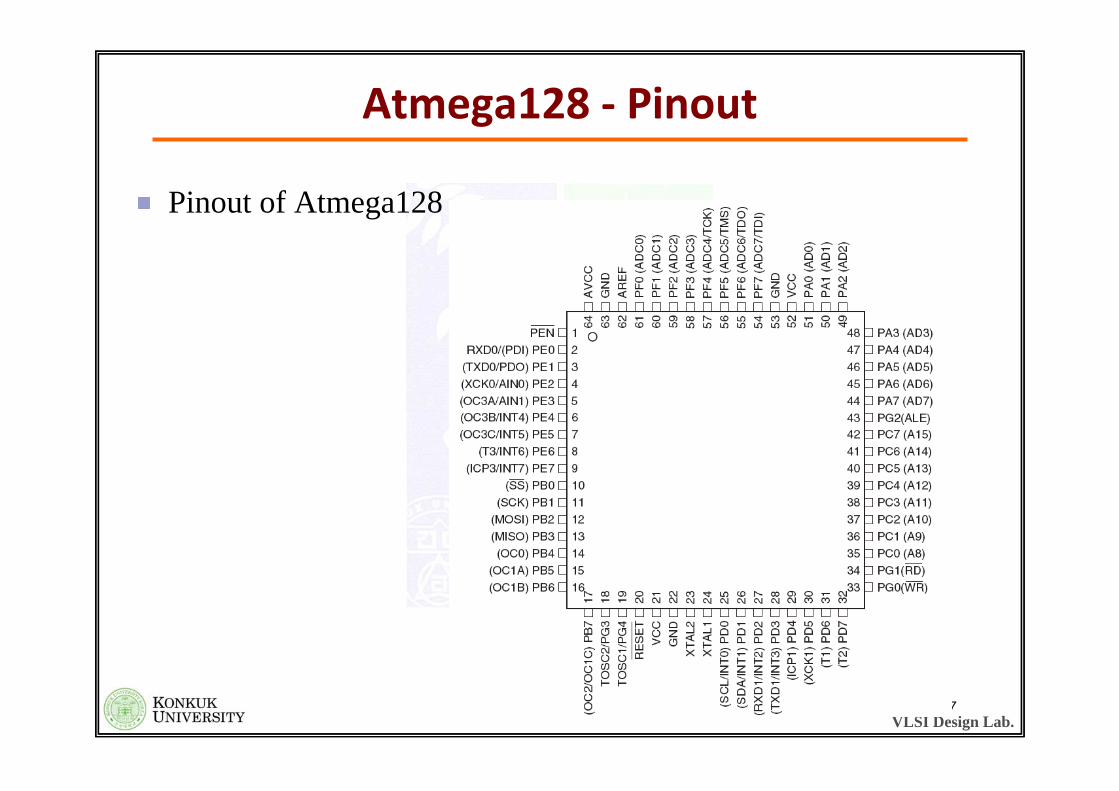
Atmega128 ‐ Pinout
Pinout of Atmega128
8VLSI Design Lab.
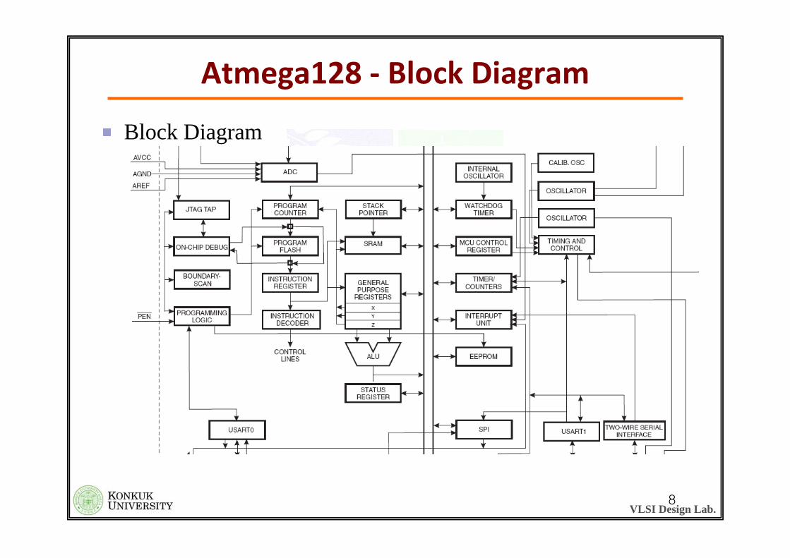
Atmega128 ‐ Block Diagram
Block Diagram
9VLSI Design Lab.
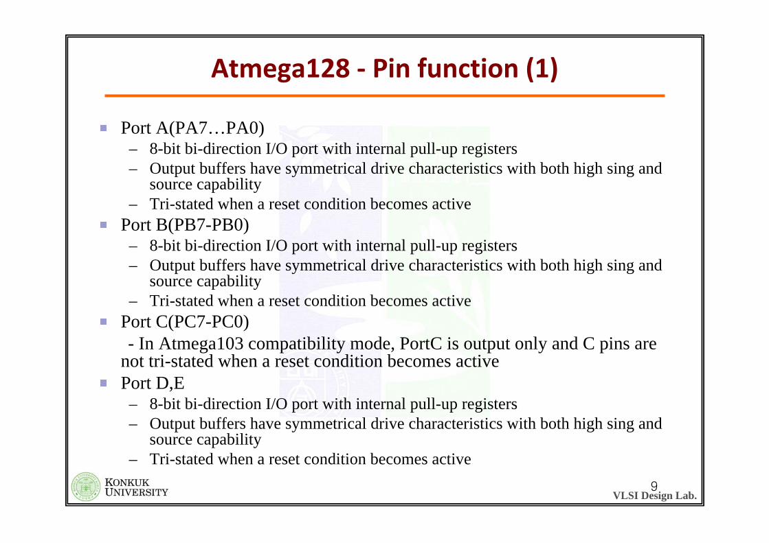
Atmega128 ‐ Pin function (1)
Port A(PA7…PA0)– 8-bit bi-direction I/O port with internal pull-up registers– Output buffers have symmetrical drive characteristics with both high sing and
source capability– Tri-stated when a reset condition becomes active
Port B(PB7-PB0)– 8-bit bi-direction I/O port with internal pull-up registers– Output buffers have symmetrical drive characteristics with both high sing and
source capability– Tri-stated when a reset condition becomes active
Port C(PC7-PC0)- In Atmega103 compatibility mode, PortC is output only and C pins are
not tri-stated when a reset condition becomes activePort D,E– 8-bit bi-direction I/O port with internal pull-up registers– Output buffers have symmetrical drive characteristics with both high sing and
source capability– Tri-stated when a reset condition becomes active
10VLSI Design Lab.
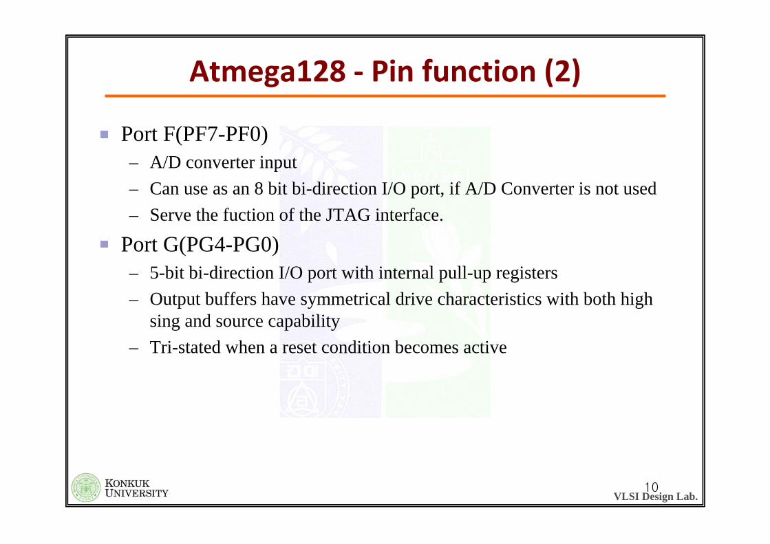
Atmega128 ‐ Pin function (2)
Port F(PF7-PF0)– A/D converter input– Can use as an 8 bit bi-direction I/O port, if A/D Converter is not used– Serve the fuction of the JTAG interface.
Port G(PG4-PG0)– 5-bit bi-direction I/O port with internal pull-up registers– Output buffers have symmetrical drive characteristics with both high
sing and source capability– Tri-stated when a reset condition becomes active

11VLSI Design Lab.
Atmega128 ‐ Pin function (3)
/PEN (Program Enable)– Pin number : 1– For SP1 Serial Programming mode and is internally pulled high – Holding this pin low during a Power-on Reset
AREF (analog reference pin )– Pin number : 62– Analog reference pin for the A/C Converter
/AVCC – Pin number : 64– Supply voltage pin for PORT F and A/D converter
RST (Reset)– Pin number : 20– Master reset
XTAL1, XTAL2– Pin number : 23,24– Oscillator input
12VLSI Design Lab.
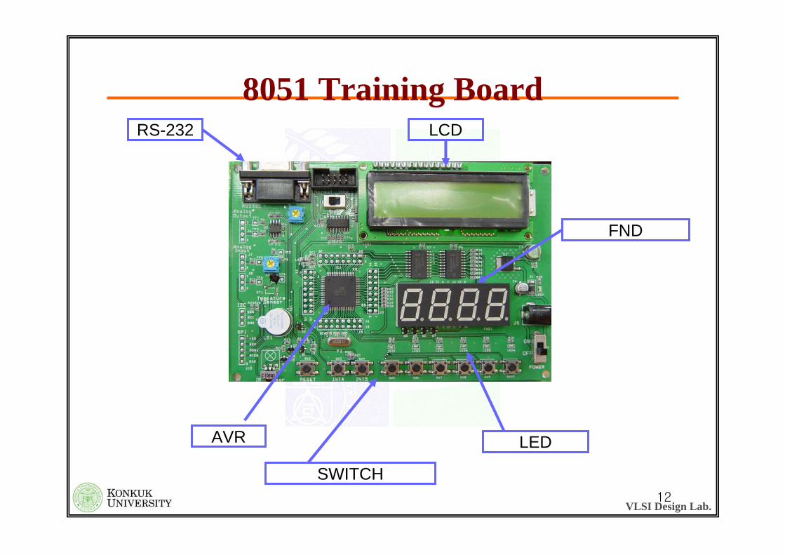
8051 Training Board
FND
AVR LED
SWITCH
LCDRS-232
13VLSI Design Lab.
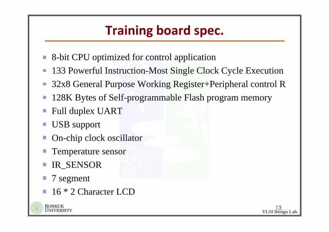
Training board spec.
8-bit CPU optimized for control application133 Powerful Instruction-Most Single Clock Cycle Execution32x8 General Purpose Working Register+Peripheral control R128K Bytes of Self-programmable Flash program memoryFull duplex UARTUSB supportOn-chip clock oscillatorTemperature sensorIR_SENSOR7 segment16 * 2 Character LCD
14VLSI Design Lab.
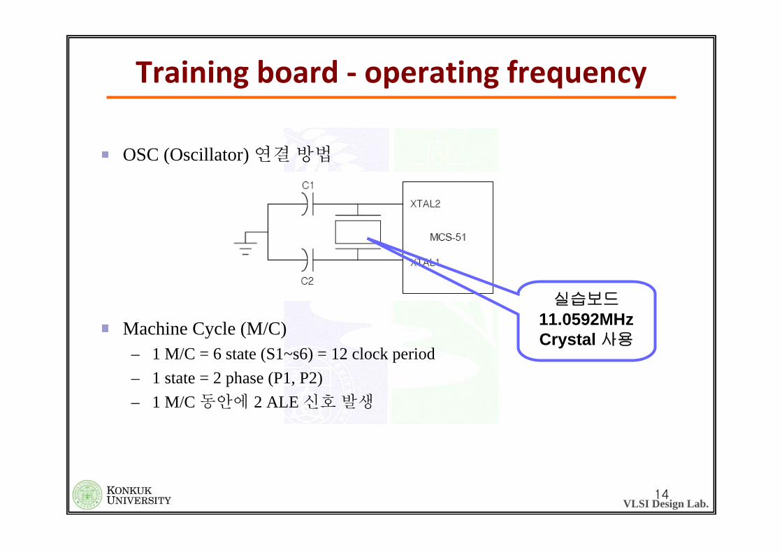
Training board ‐ operating frequency
OSC (Oscillator) 연결방법
Machine Cycle (M/C)– 1 M/C = 6 state (S1~s6) = 12 clock period– 1 state = 2 phase (P1, P2)– 1 M/C 동안에 2 ALE 신호발생
실습보드11.0592MHz Crystal 사용
15VLSI Design Lab.
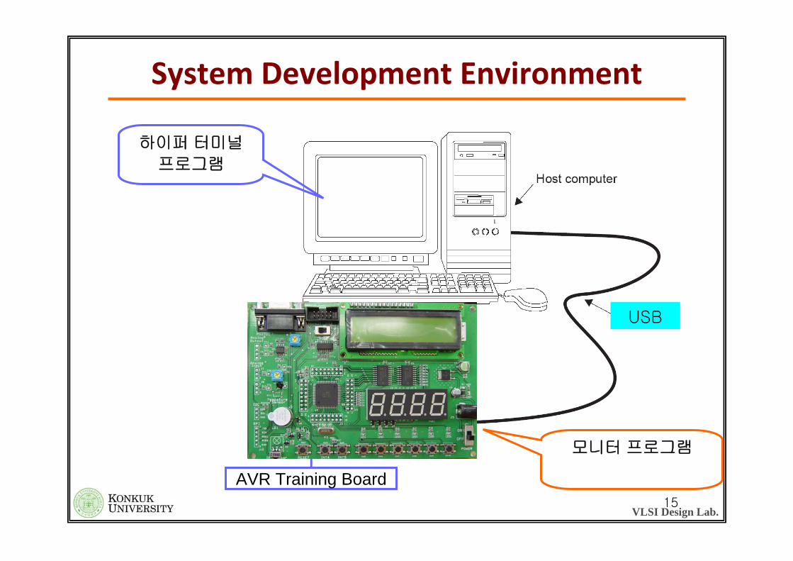
System Development Environment
AVR Training Board
하이퍼터미널
프로그램
USB
모니터프로그램
16VLSI Design Lab.
Appendix
Schematic of Training Board
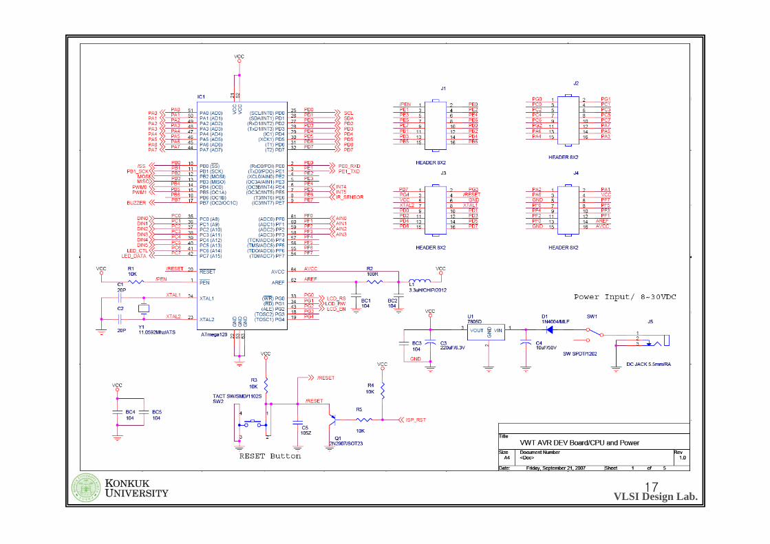
17VLSI Design Lab.
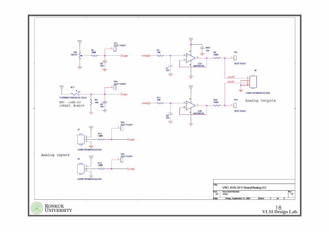
Appendix
Schematic of Training Board
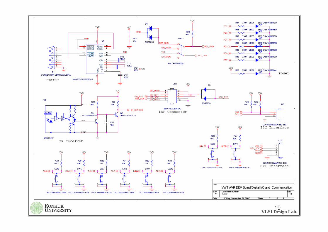
18VLSI Design Lab.
Appendix
Schematic of Training Board
19VLSI Design Lab.
Appendix
Schematic of Training Board

20VLSI Design Lab.
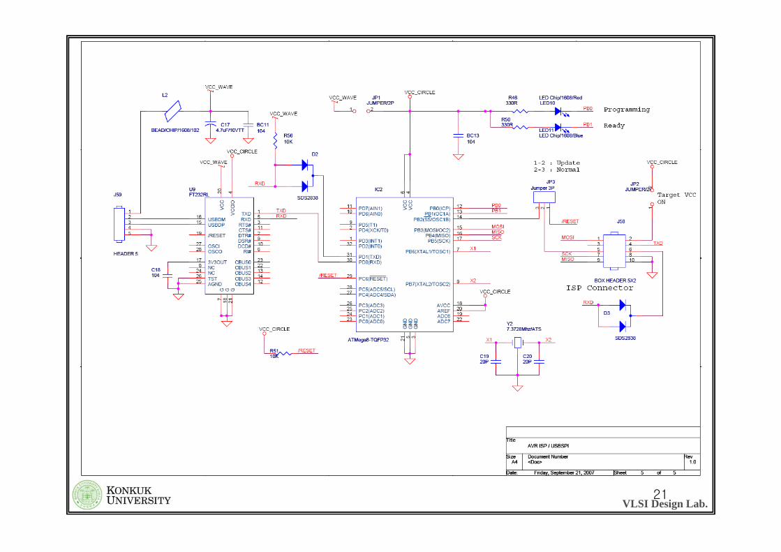
Appendix
Schematic of Training Board
21VLSI Design Lab.
Appendix
Schematic of Training Board


![09 Lecture [호환 모드] - Konkukhome.konkuk.ac.kr/~parkyong/Classes/chapter 9.pdf · and we would expect the smallest one ... A Substitution Reaction A tertiary alkyl halide and](https://img.dokumen.tips/doc/110x75/5ad7ae727f8b9a3e578c9016/09-lecture-parkyongclasseschapter-9pdfand-we-would-expect-the.jpg)


![Network Systems - chapter4.ppt [호환 모드] - Konkukhome.konkuk.ac.kr/~parkjk/courses/2015fall/network/Network Systems... · 20. Router Architecture Overview ... see chapter 5](https://img.dokumen.tips/doc/110x75/5b5918b07f8b9a31668cb65a/network-systems-konkukhomekonkukackrparkjkcourses2015fallnetworknetwork.jpg)