Embed Size (px)
Citation preview

EE215A B. Razavi Fall 11 HO #2
1
Why Analog? - Naturally-occurring signals, e.g., voice and video, are analog. - System and medium non-idealities often make it necessary to treat
digital signals as analog: o Data Retrieved from Disk
o Digital Wireless Communications Why is analog design such a big deal? - Entails more trade-offs than digital design: Digital Analog speed power speed power - More sensitive to noise and cross-talk. - More sensitive to second-order effects in devices. - More difficult to automate. - More difficult to model and simulate. - We want to design analog circuits in mainstream VLSI technologies,
e.g., CMOS, with no additional processing steps, trimming, factory calibration, etc.
EE215A B. Razavi Fall 11 HO #2
2
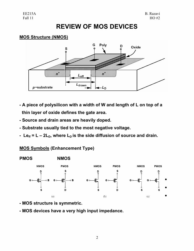
REVIEW OF MOS DEVICES MOS Structure (NMOS)
- A piece of polysilicon with a width of W and length of L on top of a thin layer of oxide defines the gate area. - Source and drain areas are heavily doped. - Substrate usually tied to the most negative voltage. - Leff = L – 2LD, where LD is the side diffusion of source and drain. MOS Symbols (Enhancement Type) PMOS NMOS
•
•
•
- MOS structure is symmetric. - MOS devices have a very high input impedance.

EE215A B. Razavi Fall 11 HO #2
3
MOS characteristics o How does the device turn on and off? o What is the drain-source current when the device is on? Threshold Voltage
• For VGS < VTH, holes in substrate are repelled from gate area, leaving
negative ions behind. (No current flows because no carriers are available.) A depletion region forms under the gate.
• For VGS ≈ VTH, electrons are attracted to the interface under gate,
establishing a “channel” for conduction. The channel is also called the “inversion layer.” • For VGS ≈ VTH, depletion region under channel remains relatively
constant, but the charge in inversion layer increases . • Turn-on process not really abrupt, i.e., for VGS ≈ VTH, ID > o. => Sub-
threshold conduction (considered later). • For a long-channel device with uniform substrate doping: (and Vsub = Vsource):

EE215A B. Razavi Fall 11 HO #2
4
where • Often need to implant the channel to obtain the “right” threshold. • A helpful approximation: For VGS ≈ VTH, there is only depletion region
in the gate area; for VGS ≈ VTH, the depletion region is constant and the inversion layer charge increases. • A useful Lemma: If a conductor carries a constant current I and it has
a charge density (charge per unit length) of Qd and the charge moves with a velocity v: I = Qd v
MOS I – V Characteristics
• For VDS > o, the inversion layer charge is non-uniform:

EE215A B. Razavi Fall 11 HO #2
5
Note that as we approach the end of the channel, the charge density falls. • To find the current, multiply charge density by charge velocity. For a
semiconductor: The drain current is therefore given by
subject to boundary conditions at the two ends of the channel. Thus,
and hence,
• Assumptions made: 1. One-dimensional structure 2. Constant mobility 3. Constant depletion layer charge - For small VDS,

EE215A B. Razavi Fall 11 HO #2
6
Each line represents an ohmic resistor of Ron = Thus, a MOS device can operate as a resistor whose value is controlled
by VGS (so long as VDS << 2 (VGS ≈ VTH):
• Note that the device can be on but have zero current, which occurs
only if VDS = o. Pinch-Off • What happens if VDS > VGS - VTH?
• Electrons reach a high velocity near the end of inversion layer and shoot into depletion region around the drain.

EE215A B. Razavi Fall 11 HO #2
7
• Device has entered “Saturation Region.”
• In saturation region, ID is independent of VDS => device acts as a
current source:
Concept of Transconductance

EE215A B. Razavi Fall 11 HO #2
8
Example
Conceptual Visualization
Other Phenomena 1. Body Effect:
• As VB becomes more negative, more holes can break loose from
atoms under the gate area, leaving negative ions behind => depletion region can contribute more charge => inversion layer forms for larger VG => threshold voltage ↑

EE215A B. Razavi Fall 11 HO #2
9
2. Channel Length Modulation • As VDS ↑, the width of depletion region between inversion layer and
drain ↑ => Effective channel length ↓ = ID ↑
3. Mobility Degradation with Vertical Field As VGS ↑, vertical field ↑ => carries travel closer to interface and
experience more scattering => mobility falls: 4. Mobility Degradation with Lateral Field At high electrical fields, electrons experience substantial scattering from
lattice and eventually travel at a constant velocity: I = Qd v Consequences of Velocity Saturation: I. Drain current saturates before pinch-off => it’s lower than predicted
by square law. II. Transconductance is relatively independent of current and channel
length. Why?
EE215A B. Razavi Fall 11 HO #2
10
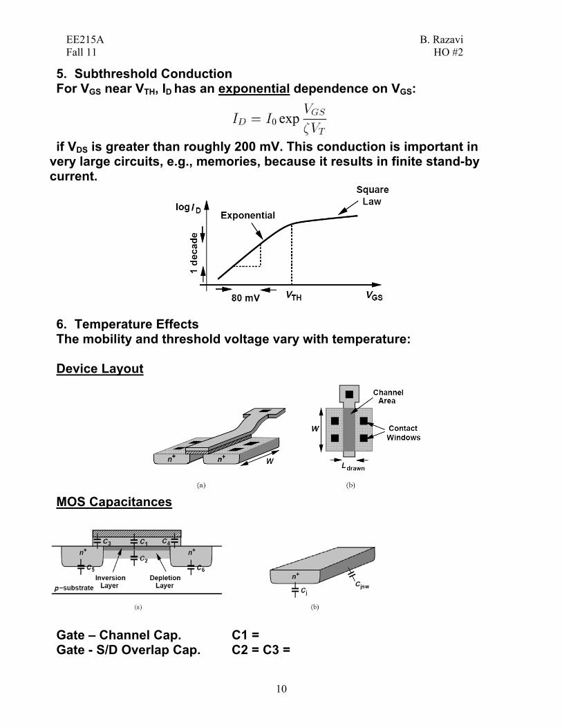
5. Subthreshold Conduction For VGS near VTH, ID has an exponential dependence on VGS:
if VDS is greater than roughly 200 mV. This conduction is important in
very large circuits, e.g., memories, because it results in finite stand-by current.
6. Temperature Effects The mobility and threshold voltage vary with temperature: Device Layout
MOS Capacitances
Gate – Channel Cap. C1 = Gate - S/D Overlap Cap. C2 = C3 =

EE215A B. Razavi Fall 11 HO #2
11
Gate – Bulk Cap. C4 = Source and drain junction caps consist of two components: sidewall and
bottom plate. Each component can be expressed as:
where m is typically between 0.3 and 0.5. The device thus looks like this:
NOTE: Depending on the region of operation (off, triode, sat.), the
equivalent capacitances between terminals assume different values.
Small-Signal Model
The model can be developed by perturbing the voltage difference between each two terminals and measuring each resulting current change.

EE215A B. Razavi Fall 11 HO #2
12
For body effect:
and hence:
Complete Model:
SPICE MOS Model The following parameters are the bare minimum SPICE needs to simulate
circuits.
Modern MOS models have several hundred parameters.
EE215A B. Razavi Fall 11 HO #2
13
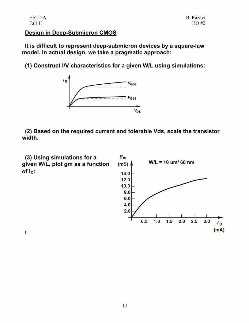
Design in Deep-Submicron CMOS It is difficult to represent deep-submicron devices by a square-law
model. In actual design, we take a pragmatic approach: (1) Construct I/V characteristics for a given W/L using simulations: (2) Based on the required current and tolerable Vds, scale the transistor
width. (3) Using simulations for a
given W/L, plot gm as a function of ID: (
W/L = 10 um/ 60 nm


![Rf microelectronics [behzad razavi , 1998]](https://img.dokumen.tips/doc/110x75/55ceee47bb61ebdb7f8b467f/rf-microelectronics-behzad-razavi-1998.jpg)

