Embed Size (px)
Citation preview

Application Specific Integrated Circuit Design
Lecture 5Vladimir Stojanoviü
6.973 Communication System Design – Spring 2006Massachusetts Institute of Technology
Cite as: Vladimir Stojanovic, course materials for 6.973 Communication System Design, Spring 2006. MIT OpenCourseWare (http://ocw.mit.edu/), Massachusetts Institute of Technology.
Downloaded on [DD Month YYYY].

Modern digital systems engineering u Managing complexity and connectivity
Personal Computer: Circuit Board:Hurdware & software =8 / system
1-166 devices
Scheme for rsprcsenting info m t i o n
Courtesy of Arvind and Krste Asanovic. Used with permission.
Integrated Circuit: \
w8-16 / PCB 0.25M-16devices &-16/IC
1OOK devices
Gate: 16-64 devices =2-16 / Cell 8 devices
Cite as: Vladimir Stojanovic, course materials for 6.973 Communication System Design, Spring 2006. MIT OpenCourseWare (http://ocw.mit.edu/), Massachusetts Institute of Technology.
Downloaded on [DD Month YYYY].
6.973 Communication System Design

Chip design styles� Full-custom
� Transistors are hand-drawn � Best performance (although almost extinct)
� Alpha processors, older Intel processors� Recent processors are semi-custom (Sun, AMD, Intel)
� Standard-Cell-based ASICs � Only use standard cells from the library � Dominant design style for non-processor, comms and multimedia
ASICs� This is what we will use in 6.973 (also used in 6.375)
� Cheaper alternatives (for small volumes) � Sea of Gates (mask-programmable gate arrays) � Field Programmable Gate Arrays (FPGA)
� On-the fly reconfigurable interconnect � Flexibility vs. cost
� Tighter control over transistors increases design cost � Can make faster designs but harder to verify and more expensive
Cite as: Vladimir Stojanovic, course materials for 6.973 Communication System Design, Spring 2006. MIT OpenCourseWare (http://ocw.mit.edu/), Massachusetts Institute of Technology.
Downloaded on [DD Month YYYY].
6.973 Communication System Design 3

Modern Application-Specific IC (ASIC)� Multiple functional blocks Our ASIC example:
� Put together at the top level 802.11a PHY � Makes a WLAN chip
� Lots of modeling � Behavioral level � Architecture/functional level Image removed due to copyright restrictions.
� Different teams on each block � Need to make sure things work
� When connected � Many levels of hierarchy
� Lots of iteration and reuse
� Many architectural choices � Use lots of implementation tricks
� Micro-architecture and algorithmic transforms [Thompson02]
� Straightforward solutions many times the chip size
� Sophisticated CAD tools to architect and verify 4M design Cite as: Vladimir Stojanovic, course materials for 6.973 Communication System Design, Spring 2006.
MIT OpenCourseWare (http://ocw.mit.edu/), Massachusetts Institute of Technology. Downloaded on [DD Month YYYY].
6.973 Communication System Design 4

Macro modules 256x32 (or 8192 bit) SRAM Generated by hard-macro module generator
Image removed due to copyright restrictions.
Generate highly regular structures (entire memories, multipliers, etc.) with a few lines of code
Verilog models for memories automatically generated based on size Example- chip-in-a-day flow (B. Brodersen, UC Berkely)
A bunch of macros pre-generated (multipliers, adders, memories) Easy to do COmm system design Courtesy of Anantha Chandrakasan. Used with permission.
Cite as: Vladimir Stojanovic, course materials for 6.973 Communication System Design, Spring 2006. MIT Opencourseware (http://ocw.mit.edu/), Massachusetts Institute of Technology.
Downloaded on [DD Month YYYY].
6.973 Communication System Design

Gate Arrays Can cut mark costs by prefabricating arrays of
transistors on wafers Only customize metal layer for each design
Image removed due to copyright restrictions.
Fixed-size unit transistors Metal connections personalize design
Two kinds: Channeled Gate Arrays - Leave space between rows of
transistors fo r routing Sea-of-Gates - Route over the top of unused
transistors
Courtesy of Arvind and Krste Asanovic. Used with permission.
[ OCEAN Sea-of -Gates Base Pattern 1
Cite as: Vladimir Stojanovic, course materials for 6.973 Communication System Design, Spring 2006. MIT OpenCourseWare (http://ocw.mit.edu/), Massachusetts Institute of Technology.
Downloaded on [DD Month YYYY].
6.973 Communication System Design

Gate Array Pros and Cons
Cheaper and quicker since less masks t o make - Can stockpile wafers with diffusion and poly finished
Memory inefficient when made from gate array - Embedded gate arrays add multiple fixed memory
blocks t o improve density (=>Structured ASICs) - Cell -based array designed t o provide efficient memory
cell (6 transistors in basic cell)
Logic slow and big due t o fixed transistors and wiring overhead - Advanced cell -based arrays hardwire logic functions
(NANDs/NORs/LUTs) which are personalized with metal
Courtesy of Arvind and Krste Asanovic. Used with permission.
Cite as: Vladimir Stojanovic, course materials for 6.973 Communication System Design, Spring 2006. MIT Opencourseware (http://ocw.mit.edu/), Massachusetts Institute of Technology.
Downloaded on [DD Month YYYY].
6.973 Communication System Design

Field-Programmable Gate Arrays (FPGA) Each cell in array contains a programmable logic function Array has programmable interconnect between logic functions Arrays mass-produced and programmed by customer after fabrication - Can be programmed by blowing fuses, loading SRAM bits, or loading
FLASH memory Overhead of programmability makes arrays expensive and slow but startup costs are low, so much cheaper than ASIC for small volumes
Image removed due to copyright restrictions.
Virtex4 FPGA Courtesy of Arvind and Krste Asanovic. Used with permission.
Cite as: Vladimir Stojanovic, course materials for 6.973 Communication System Design, Spring 2006. MIT OpenCourseWare (http://ocw.mit.edu/), Massachusetts Institute of Technology.
Downloaded on [DD Month YYYY].
6.973 Communication System Design

Xilinx Configurable logic block (CLB)� Full-add, LUT, shift, mux, xor, ff
Courtesy of Arvind and Krste Asanovic. Used with permission.
Courtesy of David B. Parlour.
Cite as: Vladimir Stojanovic, course materials for 6.973 Communication System Design, Spring 2006. MIT OpenCourseWare (http://ocw.mit.edu/), Massachusetts Institute of Technology.
Downloaded on [DD Month YYYY].
6.973 Communication System Design 9

Standard cell ASICs� Also called Cell-Based ICs (CBICs) � Fixed library of cells
� Memory generators
� Design � Cells synthesized from hardware descriptive language (Verilog,
VHDL) � Cells manually entered in a schematics � Placed and routed automatically (most desirable)
� Full set of masks for productions � Most popular today, but increasingly expensive due to mask costs
in advanced technologies � Currently a mask set is a couple $M
� FPGAs are getting increased attention
� We will use this approach Courtesy of Arvind and Krste Asanovic. Used with permission.
Cite as: Vladimir Stojanovic, course materials for 6.973 Communication System Design, Spring 2006. MIT OpenCourseWare (http://ocw.mit.edu/), Massachusetts Institute of Technology.
Downloaded on [DD Month YYYY].
6.973 Communication System Design 10

The ASIC flow Design Capture
Pre-Layout Simulation
Loaic Svnthesis
! Floordannina
3 1 1 1 1 U I Q C I U I I Placement I Physical: I
. -- . I
Circuit RoutingExtraction
.c Tapeout
Most Common DesignApproach for Designs up to 500Mhz Clock Rates
Courtesy of Anantha Chandrakasan. Used with permission.
Cite as: Vladimir Stojanovic, course materials for 6.973 Communication System Design, Spring 2006. MIT OpenCourseWare (http://ocw.mit.edu/), Massachusetts Institute of Technology.
Downloaded on [DD Month WYY].
6.973 Communication System Design

ASIC flow subset – 6.375 and 6.973
Courtesy of Arvind and Krste Asanovic. Used with permission.
Cite as: Vladimir Stojanovic, course materials for 6.973 Communication System Design, Spring 2006. MIT OpenCourseWare (http://ocw.mit.edu/), Massachusetts Institute of Technology.
Downloaded on [DD Month YYYY].
6.973 Communication System Design 12

Standard cell desian o Layout considerations
Cells have standard height but vary in width Designed t o conmct power. ground, and wells by abutment
Clock Rail (not typical
/ Cell U O Power
Rails in , on M2
\L Flip-flop
Courtesy of Arvind and Krste Asanovic. Used with permission.
Cite as: Vladimir Stojanovic, course materials for 6.973 Communication System Design, Spring 2006. MIT OpenCourseWare (http://ocw.mit.edu/), Massachusetts Institute of Technology.
Downloaded on [DD Month YYYY].
6.973 Communication System Design

Standard cell characterization Power Supply Line (V,,) Delay in (ns)! !
1 I Path I ~.ZV@C I 1.W-40°C I
3-input NAND cell (from ST Microelectronics): C = Load capacitance T = input riseffall time
Ground Supply Line (GND)
Each library cell (FF, NAND, NOR, INV, etc.) and the variations on size (strength of the gate) is fully characterized across temperature, loading, etc.
Courtesy of Anantha Chandrakasan. Used with permission.
Cite as: Vladimir Stojanovic, course materials for 6.973 Communication System Design, Spring 2006. MJT OpenCourseWare (http://ocw.mit.edu/), Massachusetts Institute of Technology.
Downloaded on [DD Month YYW].
6.973 Communication System Design

Standard cell layout methodology
Celktructuru!hldden under interconnect layers
With limlted interconnect layers, dedicated routing channels between rows of standard cells are needed
Width of the cell allowed to vary to accommodate complexity Interconnect plays a significant role in speed of a digital circuit
Courtesy of Anantha Chandrakasan. Used with permission.
Cite as: Vladimir Stojanovic, course materials for 6.973 Communication System Design, Spring 2006. MIT OpenCourseWare (http://ocw.mit.edu/), Massachusetts Institute of Technology.
Downloaded on [DD Month W].
6.973CommunicationSystem Design

More standard cell layouts
Over cell routing for 0.18pm bmctal stdcells
Courtesy of Arvind and Krste Asanovic. Used with permission.
Cite as: Vladirnir Stojanovic, course materials for 6.973 Communication System Design, Spring 2006. M I T OpenCourseWare (http://ocw,mit.edu/), Massachusetts Institute of Technology.
Downloaded on [DD Month YYYY].
6.973Communication System Design

The front-end: Verilog to ASIC layout flow� The “push-button” approach
Courtesy of Anantha Chandrakasan. Used with permission.
Cite as: Vladimir Stojanovic, course materials for 6.973 Communication System Design, Spring 2006. MIT OpenCourseWare (http://ocw.mit.edu/), Massachusetts Institute of Technology.
Downloaded on [DD Month YYYY].
6.973 Communication System Design 17

The back-end: The “Design closure” problem� Biggest problem are wires (signals and clock)
Courtesy of Anantha Chandrakasan. Used with permission.
Cite as: Vladimir Stojanovic, course materials for 6.973 Communication System Design, Spring 2006. MIT OpenCourseWare (http://ocw.mit.edu/), Massachusetts Institute of Technology.
Downloaded on [DD Month YYYY].
6.973 Communication System Design 17

Clockina Large Systems
Most large scale ASICs, and systems built with these ASICs, have several synchronous clock domains connected by asynchronous communication channels
I
7 1clockdomain 4
We'll focus on a single synchronous clock domain today Courtesy of Arvind and Krste Asanovic. Used with permission.
Cite as: Vladimlr Stojanovic, course materials for 6.973 Communication System Design, Spring 2006. MIT OpenCourseWare (http://ocw.mit.edu/), Massachusetts Institute of Technology.
Downloaded on [DD Month W].
6.973 Communication System Design
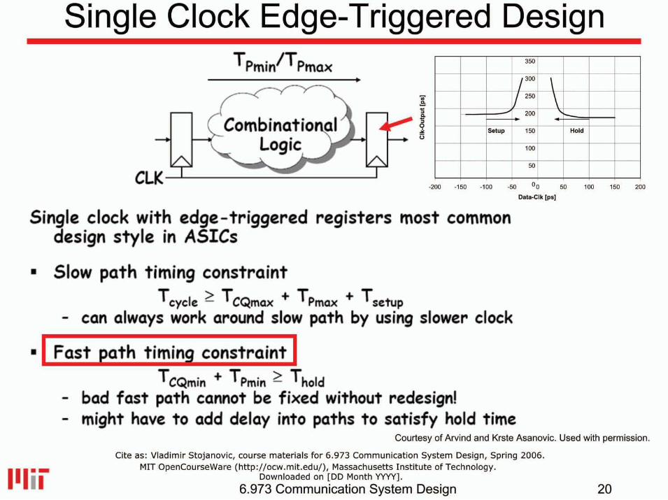
Single Clock Edge-Triggered Design
L
CLK
Single clock with edge-triggered registers most common design style in ASICs
Slow path timing constraint T-lc Tcc&wt+ TP- + Tawp- can always work around slow path by using slower clock
I Fast w t h timincl constraint I
- bad fast path camot be fixed without redesign1 - might have to add delay into paths t o satisfy hold time
Courtesy of Arvind and Krste Asanovic. Used with permission.
Cite as: Vladimir Stojanovic, course materials for 6.973 Communication System Design, Spring 2006. MIT Opencourseware (http://ocw.mit.edu/), Massachusetts Institute of Technology.
Downloaded on [DD Month YYYY].
6.973 Communication System Design

Clock distribution Can't really distribute clock a t same instant t o all flip-flops on chip
Clock Distribution jntmCe
Network length, metal width and height, ctqdi/irg caps
Clock is "clock skew" Driver Local
Clock Varrbtions in /ma/ clock Buffers
load, local power supply, local gate length and --A
threshold: lccal temprutwe Courtesy of A ~ i n dand Krste Asanovic. Used with permission.
Cite as: Vladimir Stojanovic, course materials for 6.973 Communication System Design, Spring 2006. MIT Opencourseware (http ://ocw.mit.edu/), Massachusetts Institute of Technology.
Downloaded on [DD Month YYYY].
6.973 Communication System Design

Clock grids� Alpha 21264 grid example 21064
� Minimize skew and jitter� Costs a lot of power
buffer tree
21164
Images removed due to copyright restrictions.
21264
21064 21164 21264
Cite as: Vladimir Stojanovic, course materials for 6.973 Communication System Design, Spring 2006. MIT OpenCourseWare (http://ocw.mit.edu/), Massachusetts Institute of Technology.
Downloaded on [DD Month YYYY].
6.973 Communication System Design 22

Clock treesbinary tree H-tree
Images removed due to copyright restrictions.
X-tree Arbitrary
matched tree
� Recursive pattern to match delay � Much less power than grid � More skew and jitter
� Skew� Non-uniform loading� Buffer mismatch
� Jitter� Supply noise on buffers
Cite as: Vladimir Stojanovic, course materials for 6.973 Communication System Design, Spring 2006. MIT OpenCourseWare (http://ocw.mit.edu/), Massachusetts Institute of Technology.
Downloaded on [DD Month YYYY].
6.973 Communication System Design 23

Modern Interconnect Stack
Images removed due to copyright restrictions.
Tungsten local interconnect
IBM CMOS7 process
6 layers of copper wiring
1 layer o f tungsten local interconnect Courtesy of Arvind and Krste Asanovic. Used with permission.
Cite as: Vladimir Stojanovic, course materials for 6.973 Communication System Design, Spring 2006. MIT Opencourseware (http://ocw.mit.edu/), Massachusetts Institute of Technology.
Downloaded on [DD Month YYYY].
6.973 Communication System Design

Wire resistance
Height7 width
resistance = (length x resistivity)
(height x width)
bulk aluminum bulk copper bulk silver
2 . 8 ~ 1 0 - ~n-m 1. ~ x I o - ~n-m 1 . 6 ~ 1 0 - ~n-m
Height (Thickness) fixed in given tnanufacturing process Resistances quoted as Wsquare TSMC O.18pm 6 Aluminum metal layers - MI-5 0.08 Wsquare (0.5 x lmrn wire = 160 a) - M6 0.03 SVsquare (0.5 pm x 1mm wire = 60 Q)
Courtesy of Arvind and Krste Asanovic. Used with permission.
Cite as: Vladimir Stojanovic, course materials for 6.973 Communication System Design, Spring 2006. MIT OpenCourseWare (http://ocw.mit.edu/), Massachusetts Institute of Technology.
Downloaded on [DD Month YYYY].
6.973 Communication System Design

Wire capacitance
Capacitance depends on geometry of surrounding wires and relative permittivity, &,,of insulating dielectric
- silicon dioxide, SiOp E, 3-9 - silicon flouride, SiOF E, = 3.1 - SiLKTMpolymer, E, = 2.6
Can have different materials between wires and between layers, and also different materials on higher layers
Courtesy of A ~ i n dand Krste Asanovic. Used with permission.
Cite as: Vladimir Stojanovic, course materials for 6.973 Communication System Design, Spring 2006. MIT OpenCourseWare (http://ocw.mit,edu/), Massachusetts Institute of Technology.
Downloaded on [DD Month YYYY].
6.973 Communication System Design

Capacitance scaling
parallel plate capacitance width
x lengthspacing
u width
Capacitance/wnit length -constant with feature size scaling (width and spacing scale together) - Isolated wire sees approx. 100 fF/rnrn - With close neiohbors about 160 fF/mrn
Need t o use capacitance extractor t o get accurate values
Courtesy of Arvind and Krste Asanovic. Used with permission.
Cite as: Vladimir Stojanovic, course materials for 6.973 Communication System Design, Spring 2006. MIT Opencourseware (http://ocw.mit.edu/), Massachusetts Institute of Technology.
Downloaded on [DD Month WW].
6.973 Communication System Design

Wire delay models
W i n has distributed R and C per unit length - wire delay increases quadratically with length - edge rate also degrades quadratically with length
Simple lumped n model gives reasonable approximation - Rw is lumped resistance of wire - Cw is lumped capacitance (put half at each end)
cwDelay = Rdriver x -+ (Rdriver +Rw) x2
Courtesy of h i n d and Krste Asanovic. Used with permission.
Cite as: Vladimir Stojanovic, course materials for 6.973 Communication System Design, Spring 2006. MIT OpenCourseWare (http://ocw.mit.edu/), Massachusetts Institute of Technology.
Downloaded on [DD Month YYYY].
6.973Communication Svstem Desian

Wire delay example -our technology
I n 0.18prn TSMC, 5x minimum inverter with effective resistance of 3 kn, driving F04 load (25fF) Delay = Rdriver x Cload = 75 ps
Now add lmrn M1 wire. 0.25prn wide - Rw = 320R wire + 22n vias = 344Q - CW = 160fF
Courtesy of Awind and Krste Asanovic. Used with permission.
Cite as: Vladimir Stojanovic, course materials for 6.973 Communication System Design, Spring 2006. MIT OpenCourseWare (http://ocw,rnit.edu/), Massachusetts Institute of Technology.
Downloaded on [DD Month YYYY].
6.973 Communication System Design

Wire delay scaling, local wires
For wire crossing same amount of circuitry - Resistance stays roughly constant
length decreases by saw amount as width, height stays large and/or change material t o copper
- Capacitance decreases by scaling factor cap/unit length constant, length decreases
Wire delay tracks improvement in gate delay
[Fnm Mark Homwitr, DAC ZdlXl] Courtesy of Arvind and Krste Asanovic. Used with permission.
Cite as: Vladimir Stojanovic, course materials for 6.973 Communication System Design, Spring 2006. MIT Opencourseware (http://ocw.mit.edu/), Massachusetts Institute of Technology.
Downloaded on [DD Month YYW].
6.973 Communication System Design

Wire delay scaling, global wires
For wire crossing whole chip - Resistance grows linearly - Capacitance stays fixed
Wire delay increases relative t o gate delay
[From Mork Homwitz DAC 200Y7 ] Courtesy of Arvind and Krste Asanovic. Used with permission.
Cite as: Vladimir Stojanovic, course materials for 6.973 Communication System Design, Spring 2006. MIT Opencourseware (http://ocw.mit.edu/), Massachusetts Institute of Technology.
Downloaded on [DD Month YYYY].
6.973Communication System Design

Fewer gates per clock cycle Processors in Intel 386 generation, around 50 F04 gate delays per clock cycle
Pentium-4 around 16 F04 in normal clock, around 8 F04 delays in fast ALU section
Fastest 64-bit adder around 7 F04 delays
As measured in distance per clock cycle, wires are getting much slower
Chip area traversed,, in one clock cycle
Courtesy of Arvind and Krste Asanovic. Used with permission.
Cite as: Vladimir Stojanovic, course materials for 6.973 Communication System Design, Spring 2006. MIT Opencourseware (http://ocw.mit.edu/), MassachusettsInstitute of Technology.
Downloaded on [DD Month YYYY].
6.973 Communication System Design