Embed Size (px)
Citation preview
An Introduction to GaN-on-Si Power Device Technology
���������������� � � � �� � � �� � � �� � � �
� � � �
� � � � � � �� � � � � � �� � � � � � �� � � � � � �
Outline
• Why GaN on Si for Power Device Application
• Epitaxial and Device Design Concepts
• Current Market & Technology Development Status
Why GaN on Si for Power Device Application
4
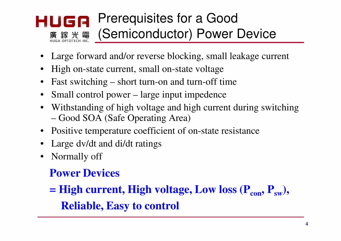
Prerequisites for a Good (Semiconductor) Power Device
• Large forward and/or reverse blocking, small leakage current• High on-state current, small on-state voltage• Fast switching – short turn-on and turn-off time• Small control power – large input impedence• Withstanding of high voltage and high current during switching
– Good SOA (Safe Operating Area)• Positive temperature coefficient of on-state resistance• Large dv/dt and di/dt ratings• Normally off
Power Devices = High current, High voltage, Low loss (Pcon, Psw),
Reliable, Easy to control
5
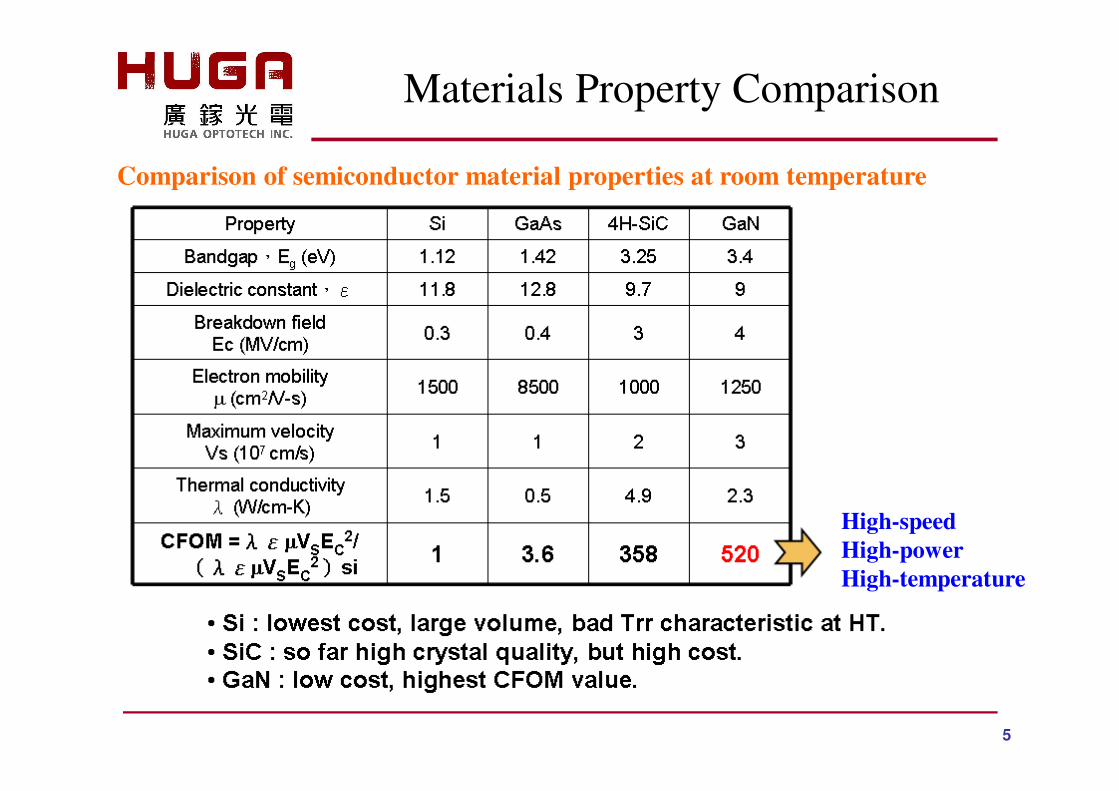
Materials Property Comparison
High-speedHigh-powerHigh-temperature
Comparison of semiconductor material properties at room temperature
66
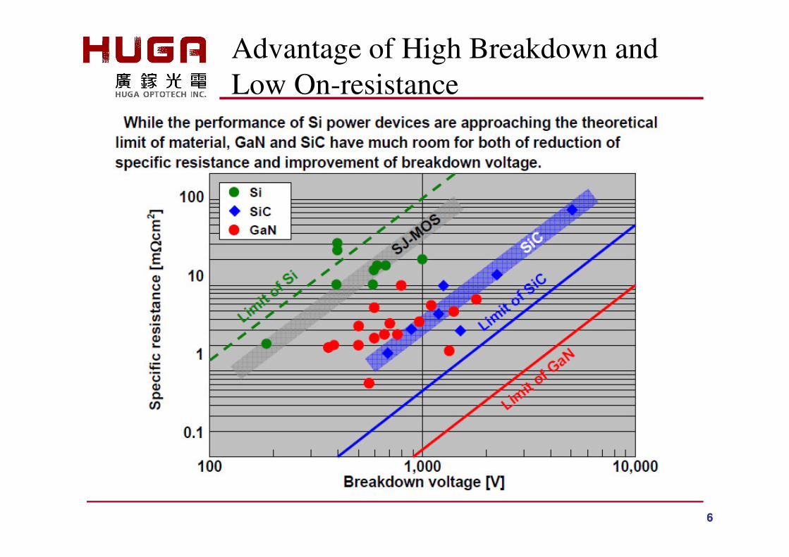
Advantage of High Breakdown and Low On-resistance
7
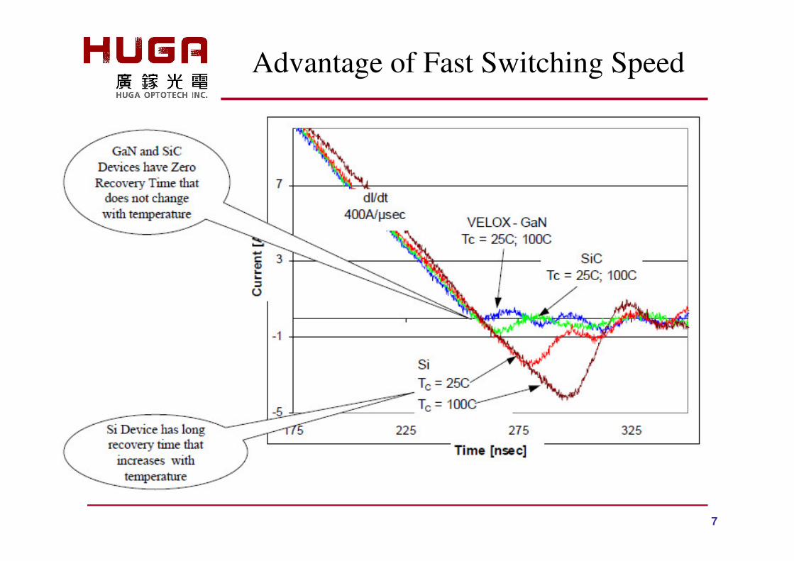
Advantage of Fast Switching Speed
88
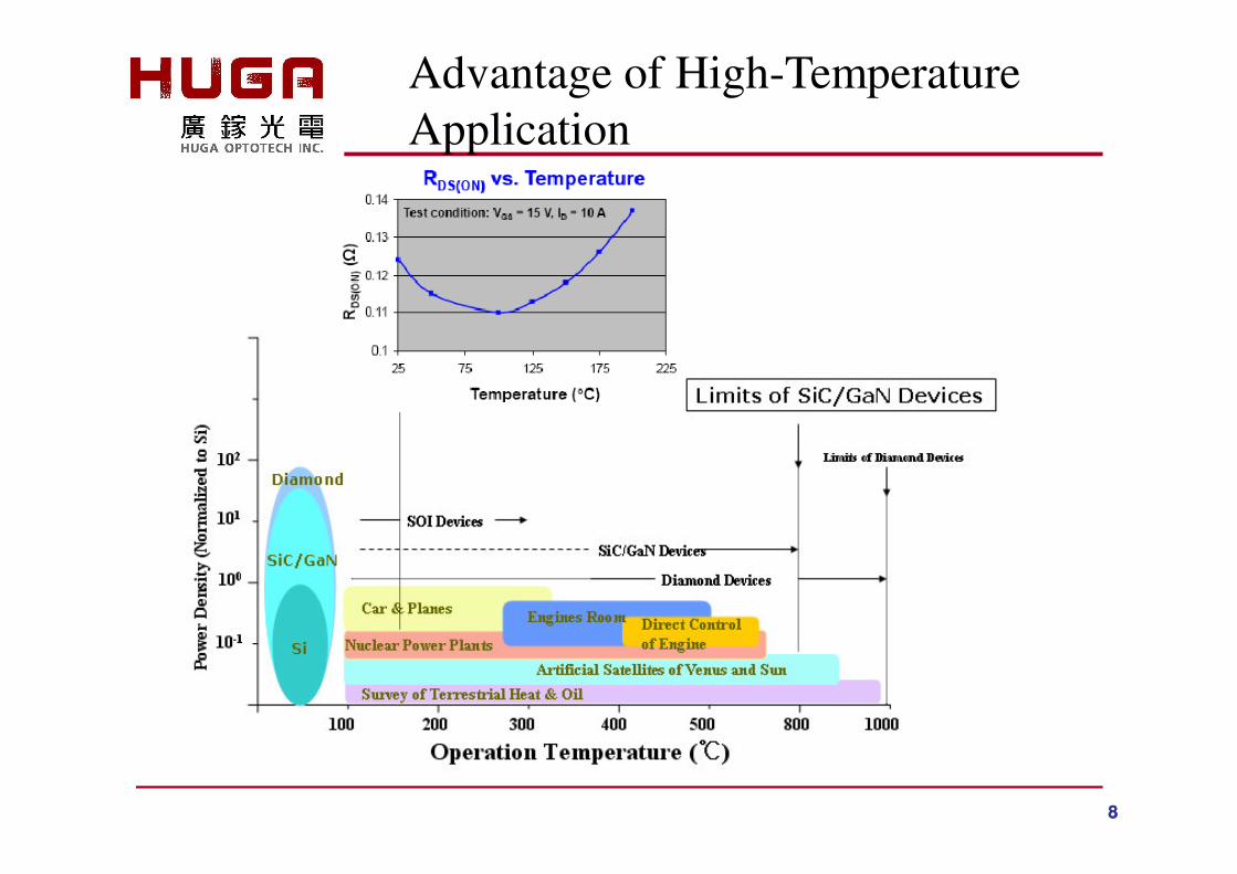
Advantage of High-Temperature Application
99
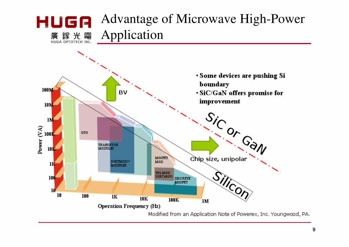
Advantage of Microwave High-Power Application
10
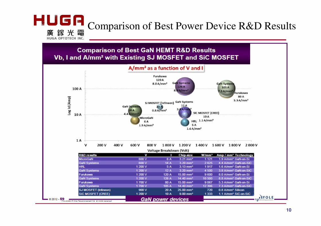
Comparison of Best Power Device R&D Results
11
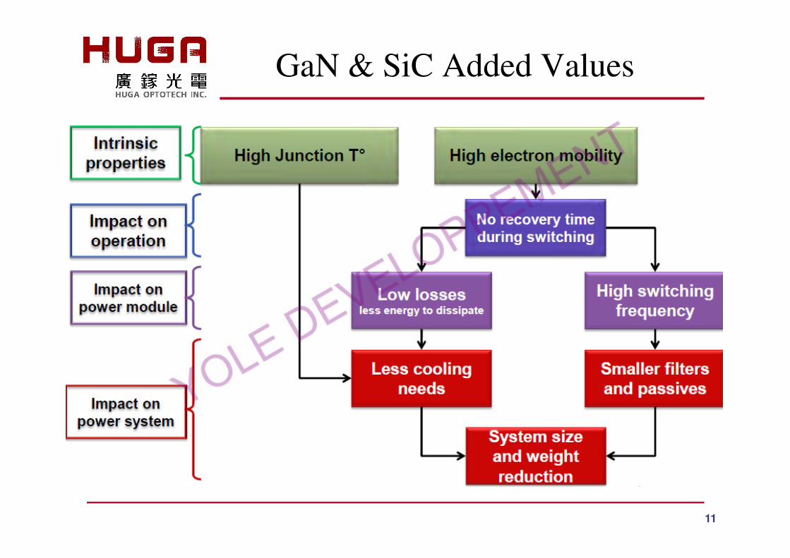
GaN & SiC Added Values
12
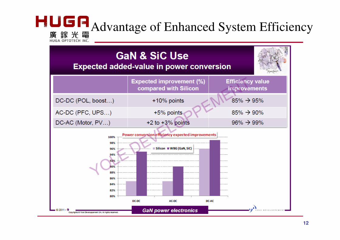
Advantage of Enhanced System Efficiency
13
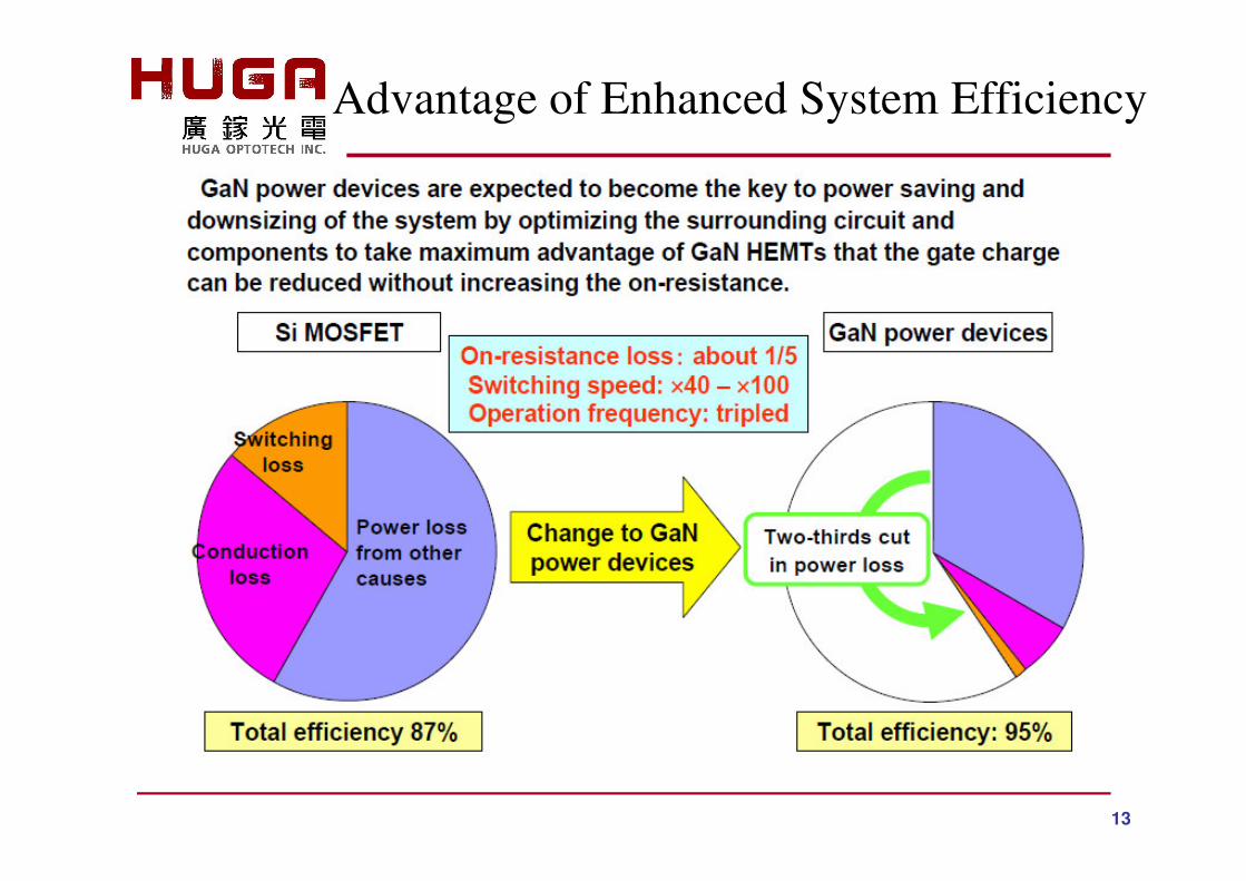
Advantage of Enhanced System Efficiency
1414
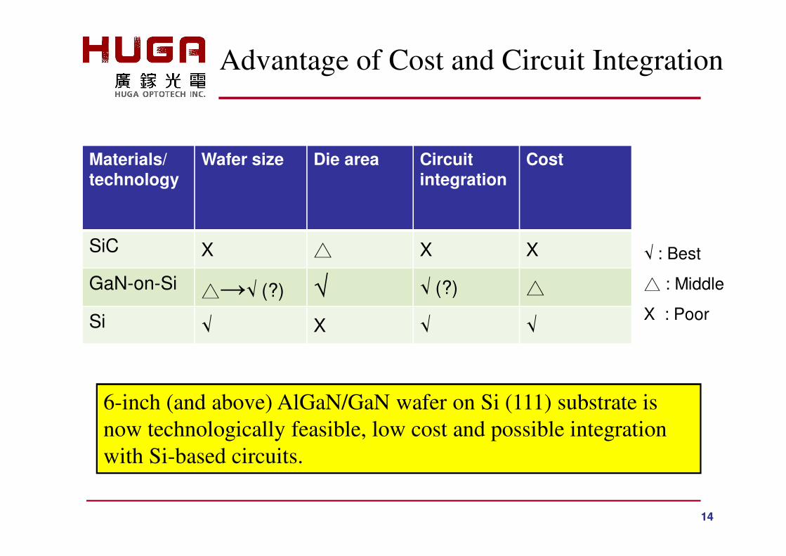
Advantage of Cost and Circuit Integration
6-inch (and above) AlGaN/GaN wafer on Si (111) substrate is now technologically feasible, low cost and possible integration with Si-based circuits.
Materials/ technology
Wafer size Die area Circuit integration
Cost
SiC X � X X
GaN-on-Si �→√ (?) √ √ (?) �
Si √ X √ √
√ : Best
� : Middle
X : Poor
15
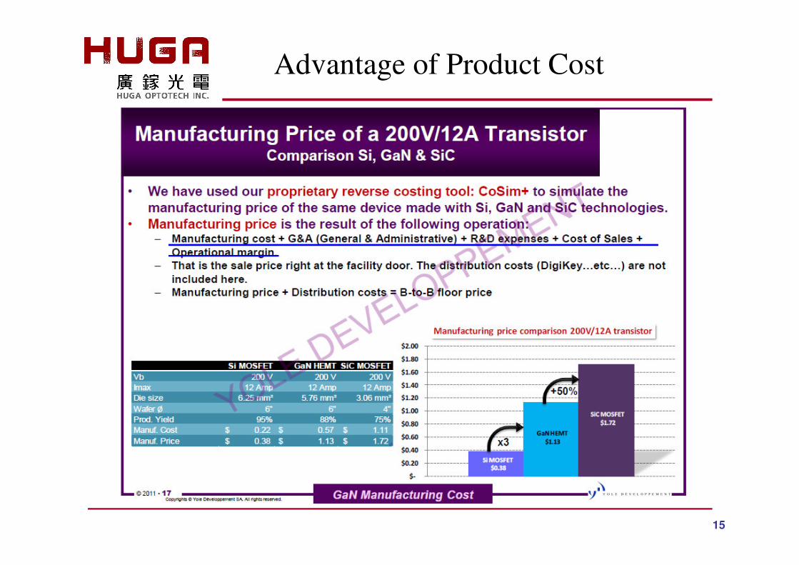
Advantage of Product Cost
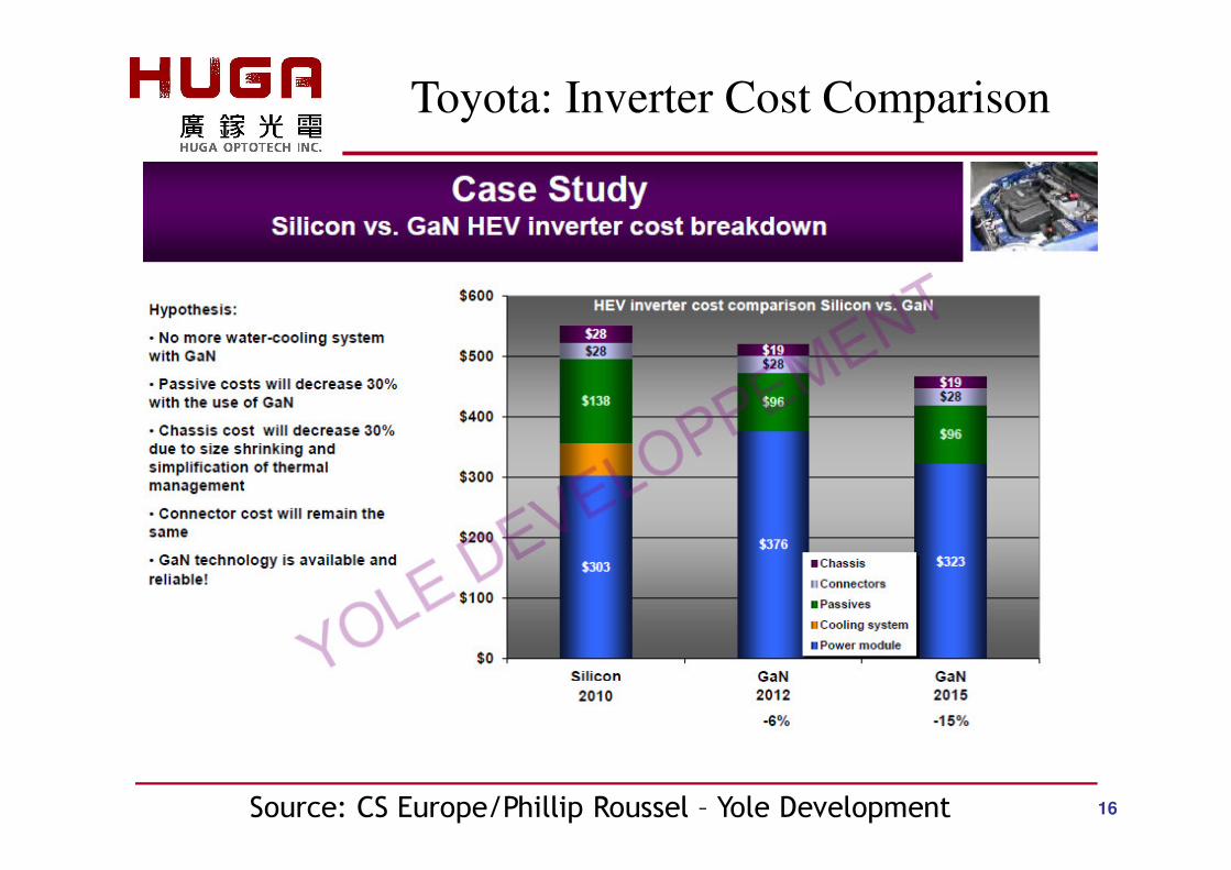
16Source: CS Europe/Phillip Roussel – Y ole D ev elopm en t
Toyota: Inverter Cost Comparison
Epitaxial and Device Design Concepts
17
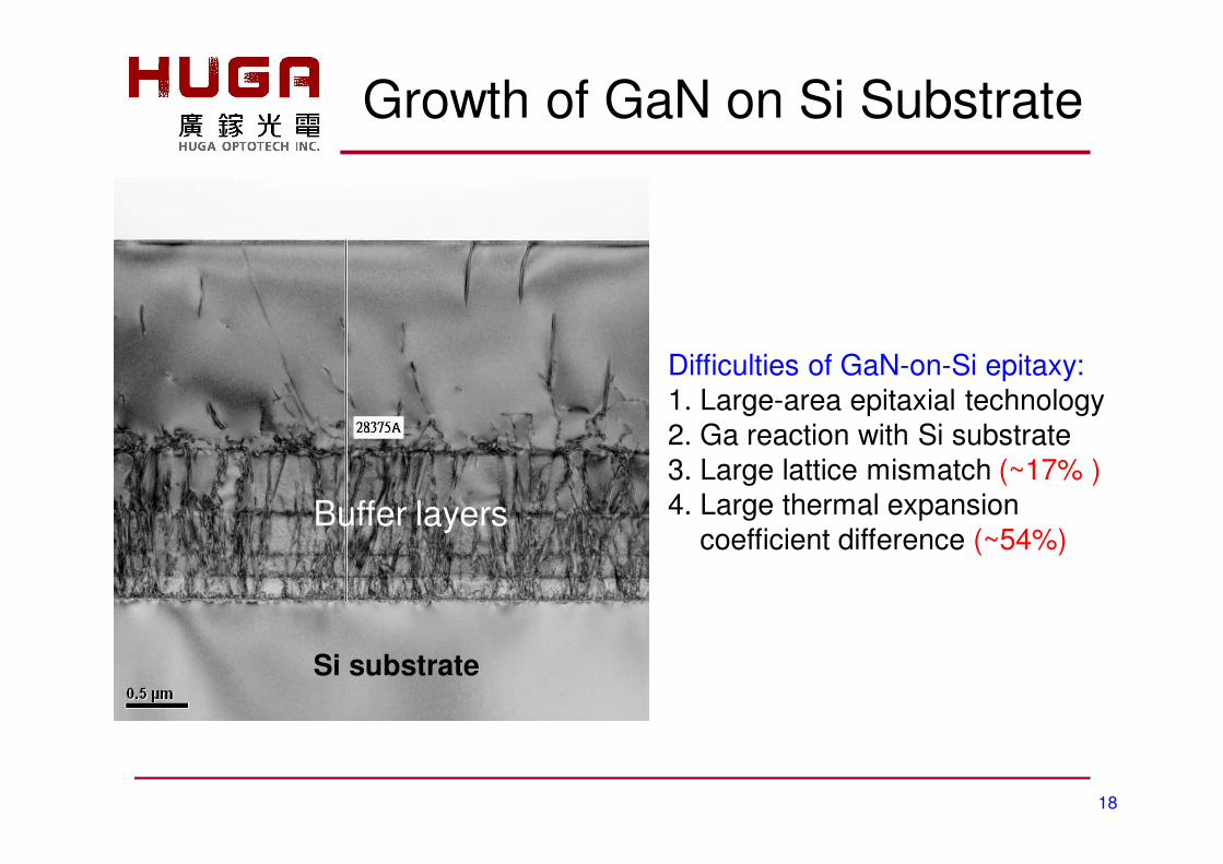
Growth of GaN on Si Substrate
18
Difficulties of GaN-on-Si epitaxy:1. Large-area epitaxial technology2. Ga reaction with Si substrate3. Large lattice mismatch (~17% )4. Large thermal expansion
coefficient difference (~54%)
Si substrate
Buffer layers
19
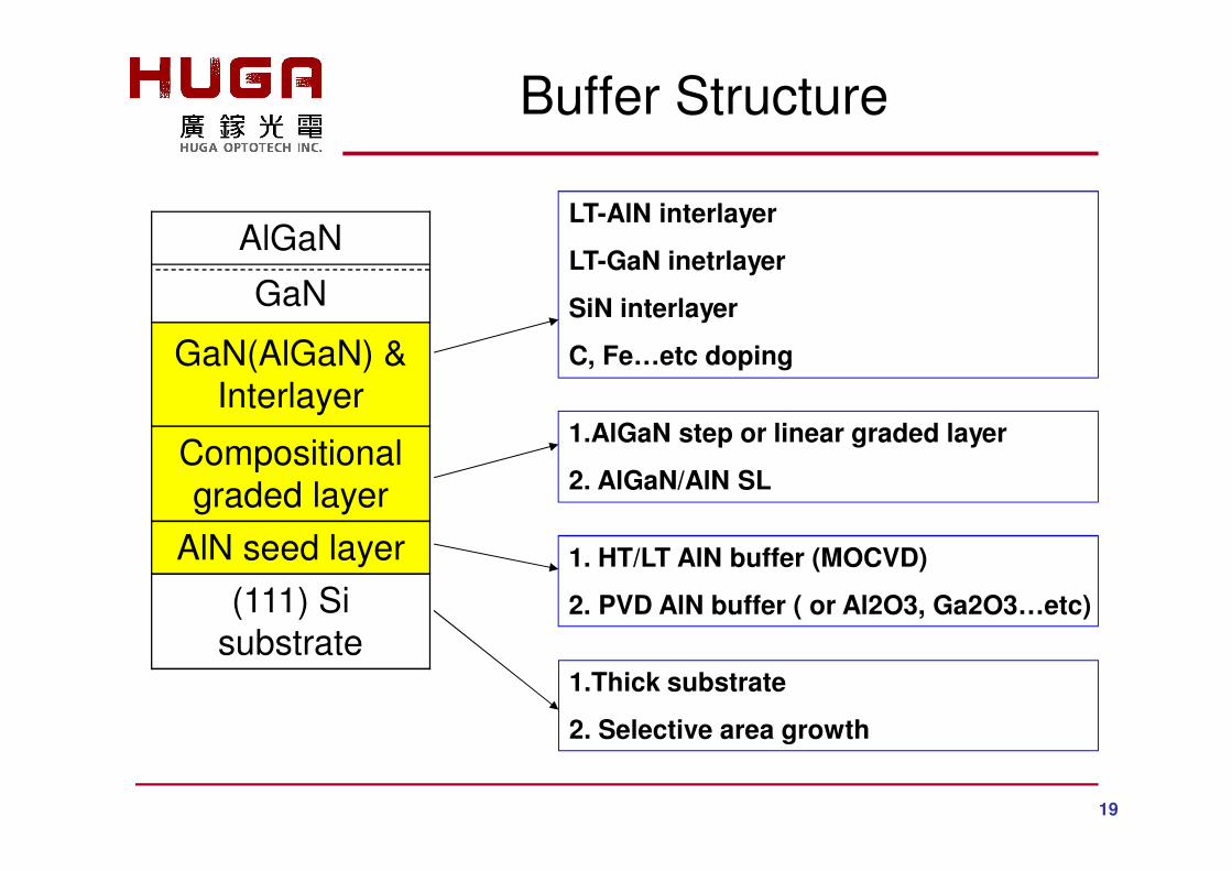
Buffer Structure
AlGaN
GaN
GaN(AlGaN) & Interlayer
Compositional graded layer
AlN seed layer(111) Si
substrate1.Thick substrate
2. Selective area growth
1. HT/LT AlN buffer (MOCVD)
2. PVD AlN buffer ( or Al2O3, Ga2O3…etc)
1.AlGaN step or linear graded layer
2. AlGaN/AlN SL
LT-AlN interlayer
LT-GaN inetrlayer
SiN interlayer
C, Fe…etc doping
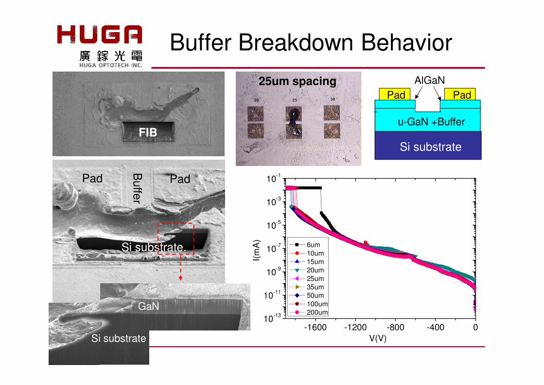
Buffer Breakdown Behavior
Si substrate
u-GaN +Buffer
Pad
Si substrate.
Pad Pad
Si-sub.GaN
Si substrate-1600 -1200 -800 -400 0
10-13
10-11
10-9
10-7
10-5
10-3
10-1
I(mA
)
V(V)
6um 10um 15um 20um 25um 35um 50um 100um 200um
25um spacing
FIB
AlGaNPad
Buffer
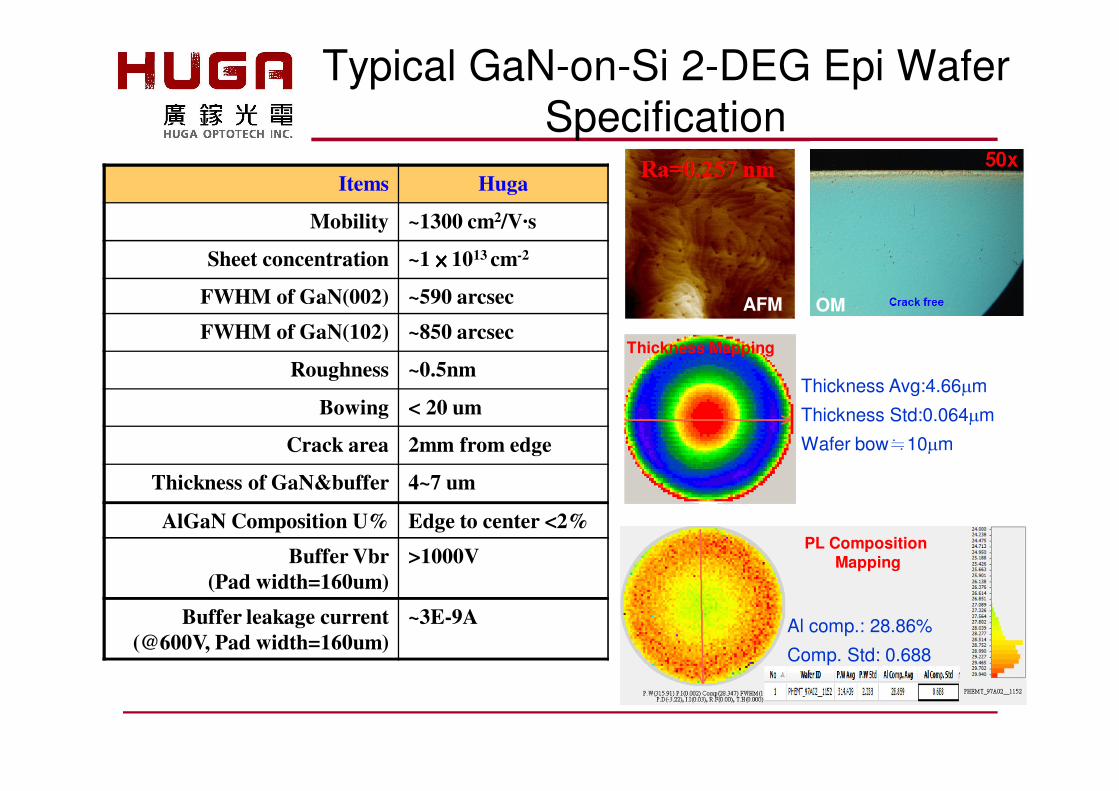
Typical GaN-on-Si 2-DEG Epi Wafer Specification
Items Huga
Mobility ~1300 cm2/V·s
Sheet concentration ~1 ���� 1013 cm-2
FWHM of GaN(002) ~590 arcsec
FWHM of GaN(102) ~850 arcsec
Roughness ~0.5nm
Bowing < 20 um
Crack area 2mm from edge
Thickness of GaN&buffer 4~7 um
AlGaN Composition U% Edge to center <2%
Buffer Vbr (Pad width=160um)
>1000V
Buffer leakage current (@600V, Pad width=160um)
~3E-9A
Thickness Avg:4.66µmThickness Std:0.064µmWafer bow�10µm
Thickness Mapping
AFM OM
Al comp.: 28.86%
Comp. Std: 0.688
PL Composition Mapping
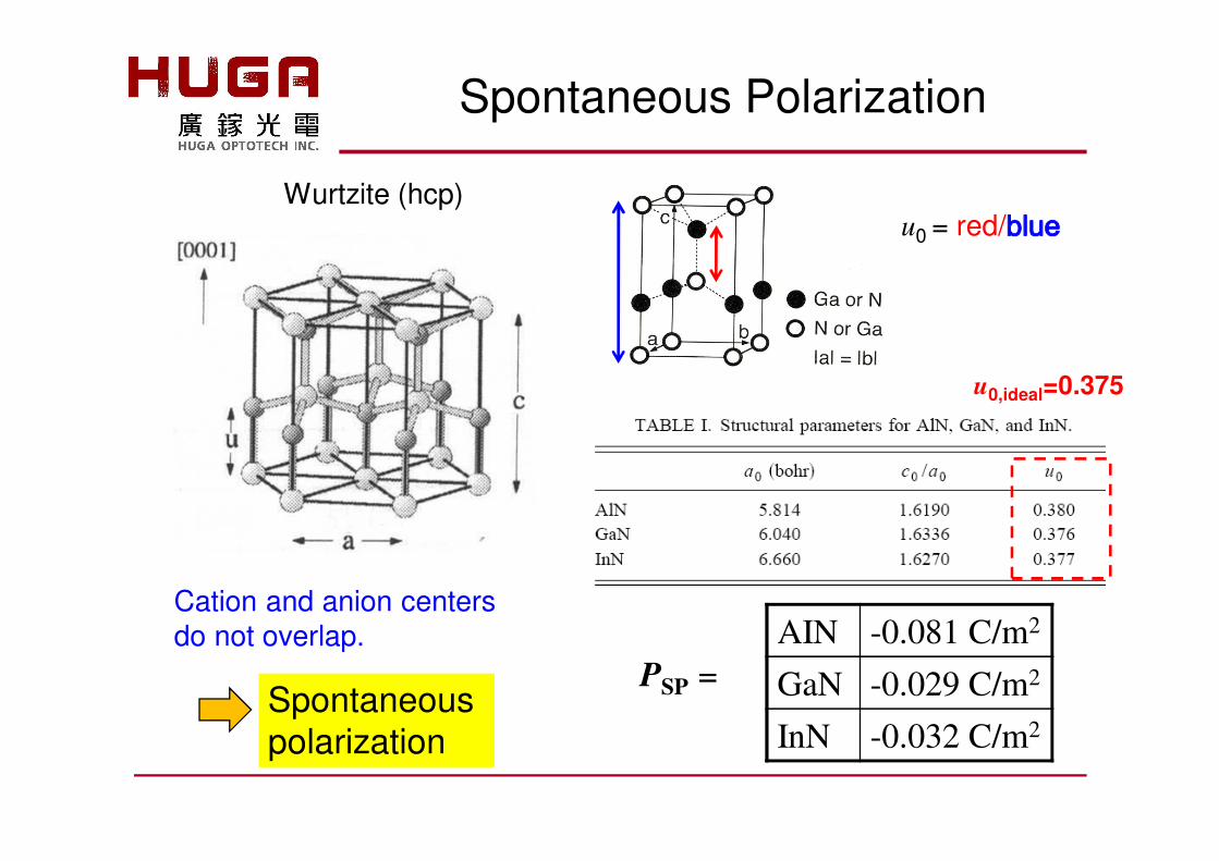
Wurtzite (hcp)
Spontaneous Polarization
Cation and anion centers do not overlap.
Spontaneous polarization
u0 = red/
u0,ideal=0.375
AIN -0.081 C/m2
GaN -0.029 C/m2
InN -0.032 C/m2
PSP =
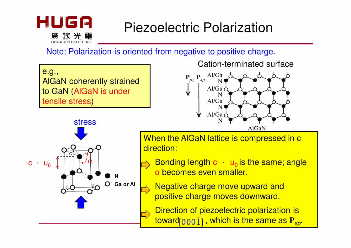
Note: Polarization is oriented from negative to positive charge.
e.g., AlGaN coherently strained to GaN (AlGaN is under tensile stress)
Cation-terminated surface
αc � u0
When the AlGaN lattice is compressed in c direction:
Bonding length c � u0 is the same; angle α becomes even smaller.
Negative charge move upward and positive charge moves downward.
Direction of piezoelectric polarization is toward , which is the same as Psp.
Ga or AlN
stress
Piezoelectric Polarization
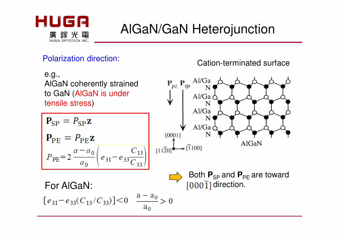
AlGaN/GaN Heterojunction
e.g., AlGaN coherently strained to GaN (AlGaN is under tensile stress)
Polarization direction:
For AlGaN:Both PSP and PPE are toward
direction.
Cation-terminated surface
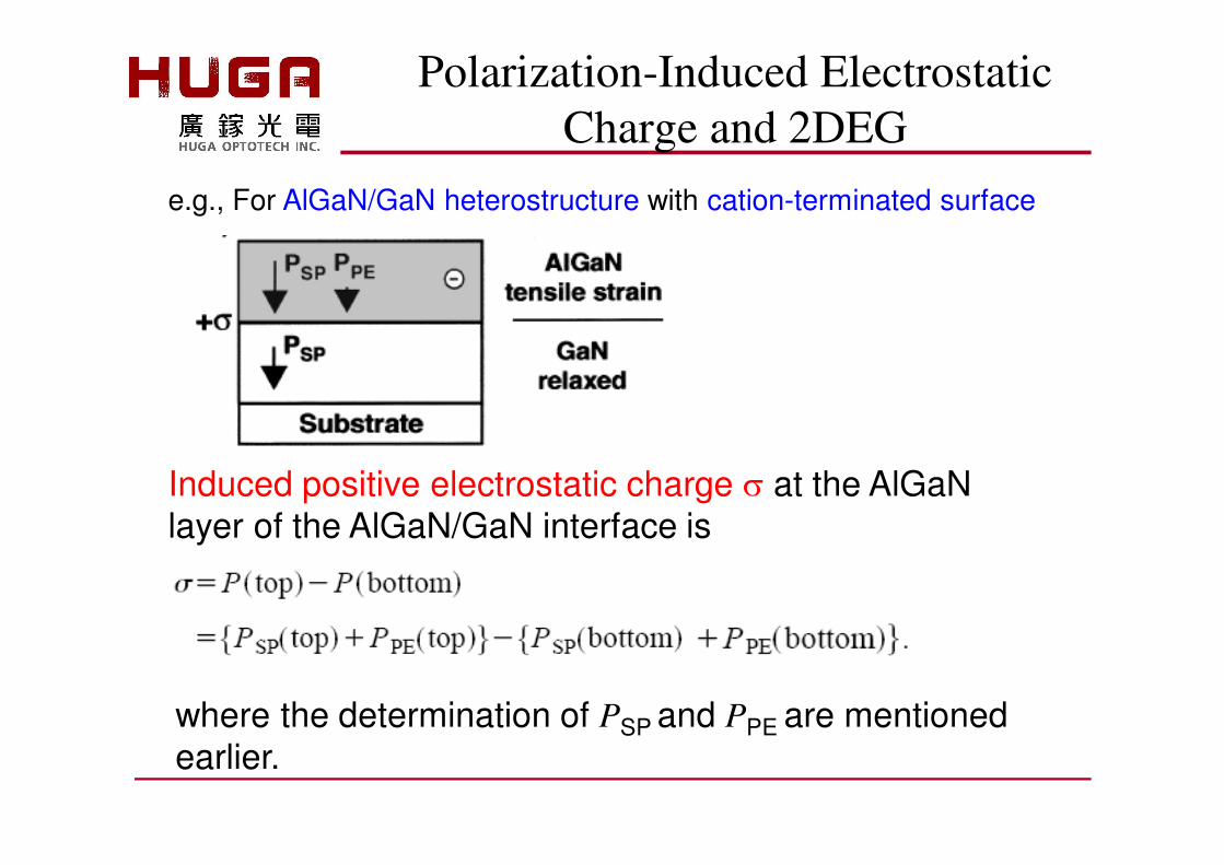
Polarization-Induced Electrostatic Charge and 2DEG
Induced positive electrostatic charge σ at the AlGaN layer of the AlGaN/GaN interface is
e.g., For AlGaN/GaN heterostructure with cation-terminated surface
where the determination of PSP and PPE are mentioned earlier.
e.g., For AlGaN/GaN heterostructure with cation-terminated surface
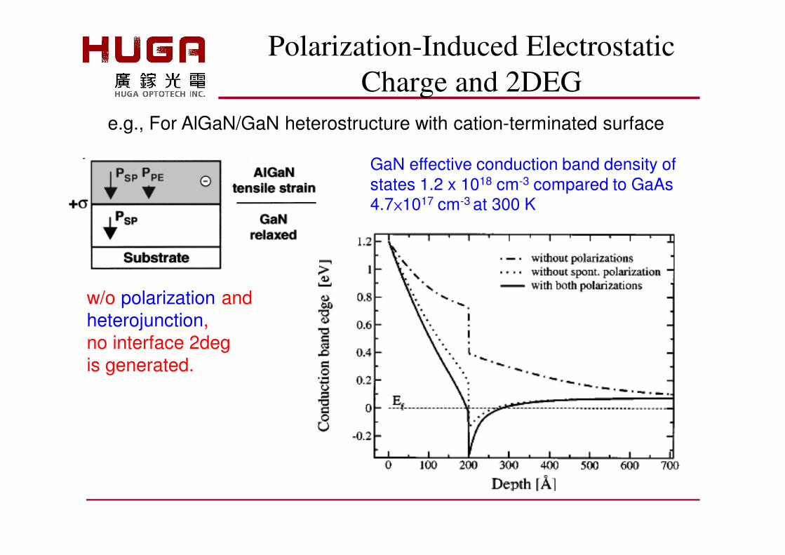
w/o polarization and heterojunction, no interface 2deg is generated.
GaN effective conduction band density of states 1.2 x 1018 cm-3 compared to GaAs4.7�1017 cm-3 at 300 K
Polarization-Induced Electrostatic Charge and 2DEG
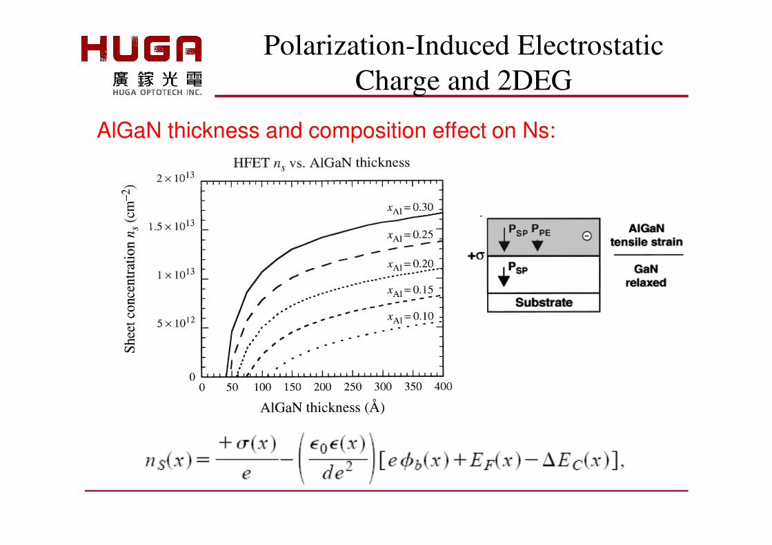
AlGaN thickness and composition effect on Ns:
Polarization-Induced Electrostatic Charge and 2DEG
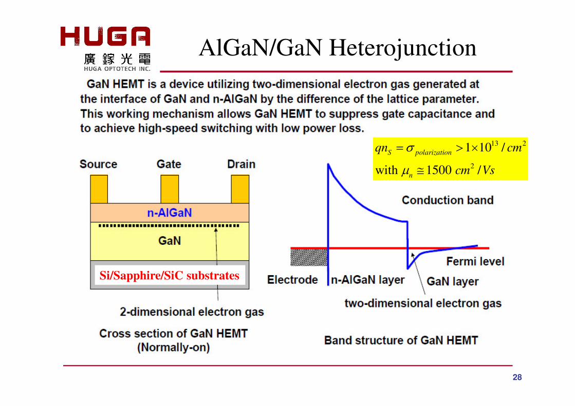
28
AlGaN/GaN Heterojunction
Si/Sapphire/SiC substrates
13 2
2
1 10 /
with 1500 /
S polarization
n
qn cm
cm Vs
σ
µ
= > ×
≅
Current Market & Technology Development Status
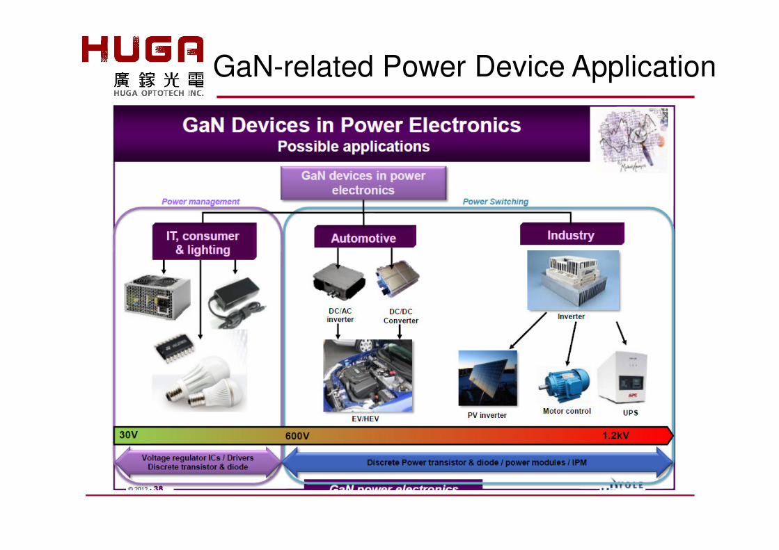
GaN-related Power Device Application
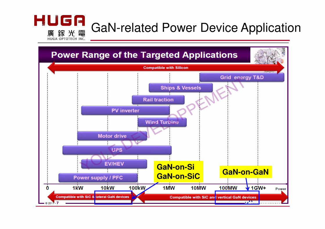
GaN-related Power Device Application
GaN-on-GaNGaN-on-SiGaN-on-SiC
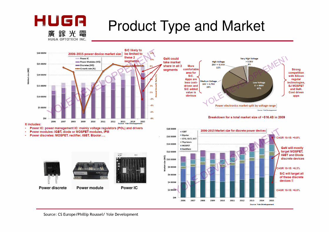
Source: CS Europe/Phillip Roussel/ Yole Development
Product Type and Market
Power ICPower modulePower discrete
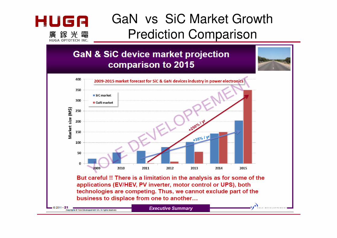
GaN vs SiC Market Growth Prediction Comparison
Source: CS Europe/Phillip Roussel/ Yole Development
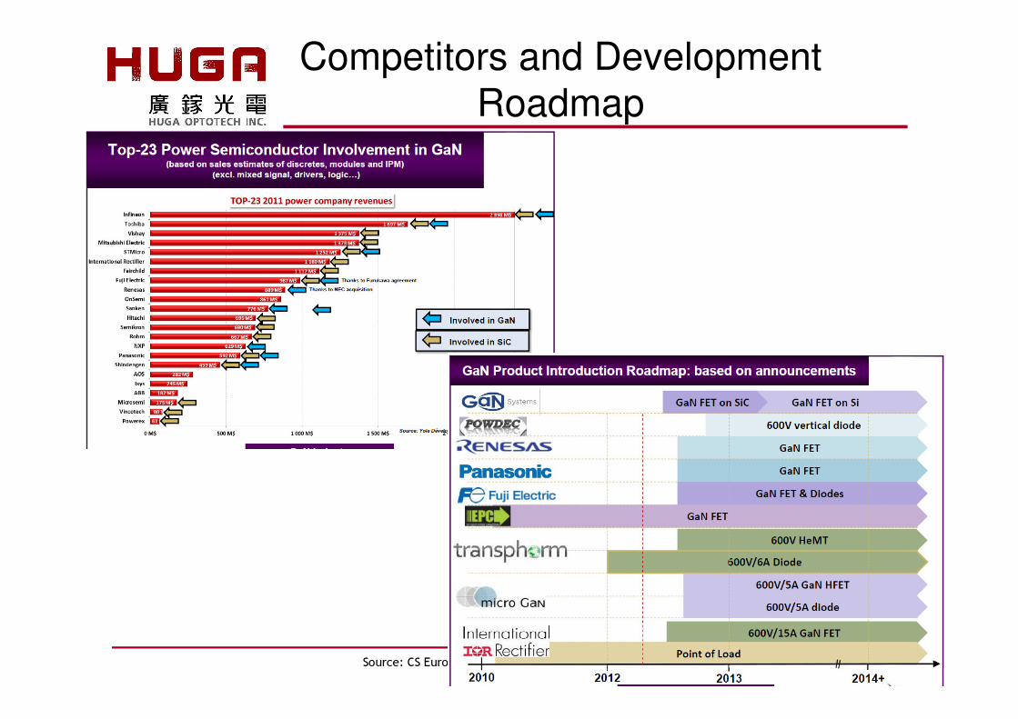
Competitors and Development Roadmap
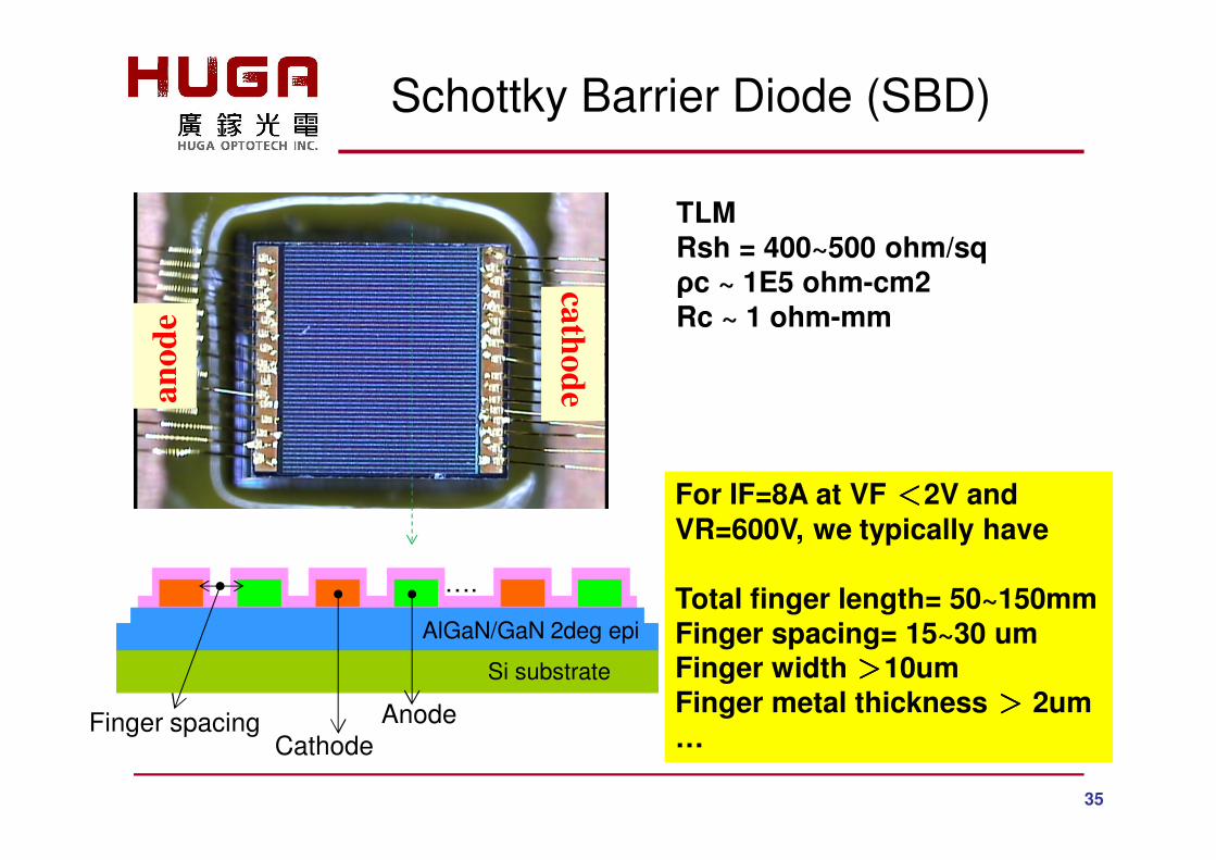
Schottky Barrier Diode (SBD)
35
cathodeanod
e
….
Si substrate
AlGaN/GaN 2deg epi
AnodeCathode
Finger spacing
For IF=8A at VF ����2V and VR=600V, we typically have
Total finger length= 50~150mmFinger spacing= 15~30 umFinger width ����10umFinger metal thickness ���� 2um…
TLMRsh = 400~500 ohm/sqρc ~ 1E5 ohm-cm2Rc ~ 1 ohm-mm
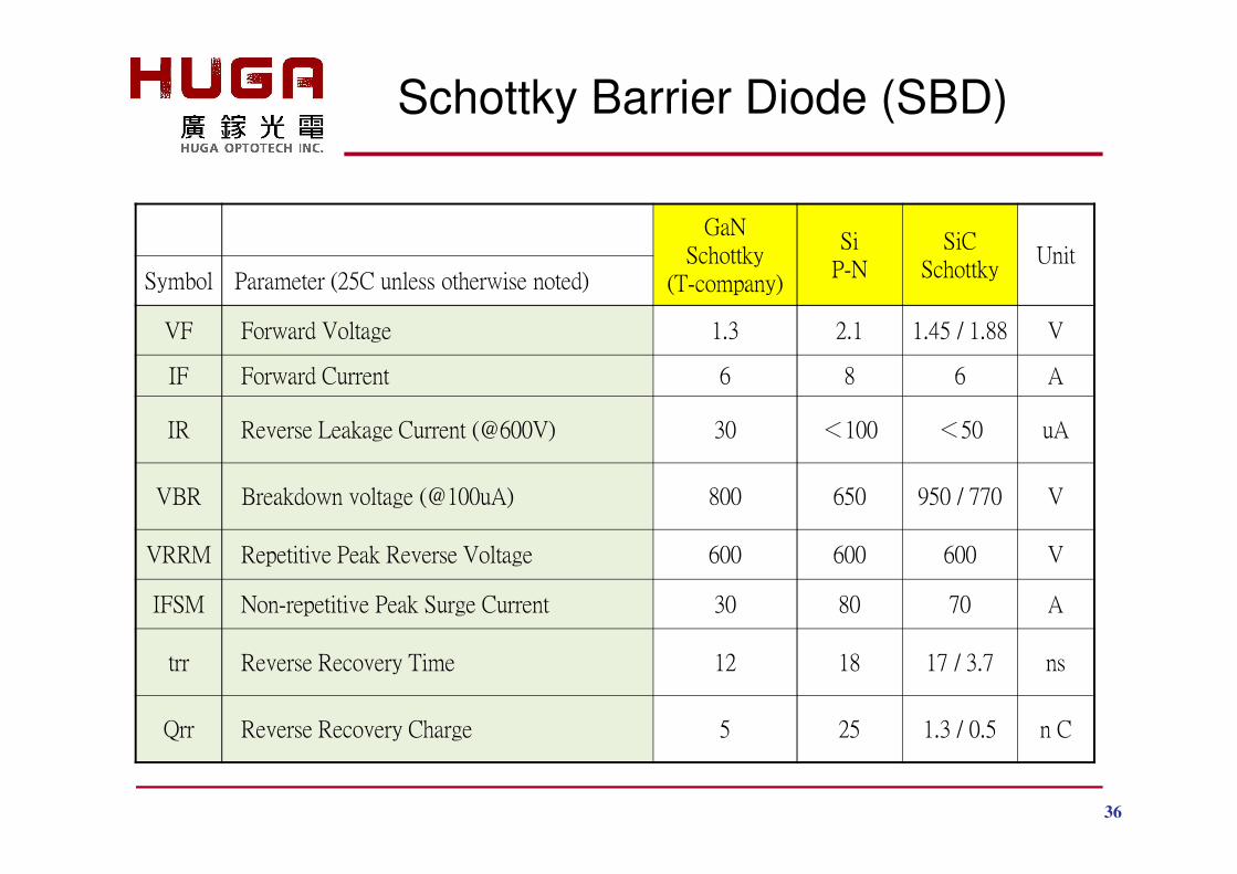
36
Schottky Barrier Diode (SBD)
���
� � � � � �
� � � � � � �� �
� � �
� �
� � �
� � � � � � � � � �
� � � � � ��� �� � � � � � � � �� � � � � � � � � � � � � � � � � � � � � � � �
!" " � � � �� � !� � � �# � $ % & � % $ $ % ' �� ( � $ % )) !
* " " � � � �� � � � � � � � � + ) + ,
* - - � . � � � � � / � � �# � � � � � � � � � � � 0 +1 1 !� & 1 2$ 1 1 2�1 � ,
!3 - 3 � � � � � � � . � � � �# � � � 0 $ 1 1 � ,� )1 1 +�1 4 �1 � ( � 5 5 1 !
!- - 6 - � � � � � � � . � � �� � � - � . � � � � � !� � � �# � +1 1 +1 1 +1 1 !
* " � 6 �� � � � � � � � � � . � � �� � � � � � # � � � � � � � � � � & 1 )1 5 1 ,
� � � - � . � � � � � - � � � . � � � � � � � $ � $ ) $ 5 � ( � & % 5 � �
7 � � - � . � � � � � - � � � . � � � � � �� # � � � � $ % & � ( � 1 % � � � �
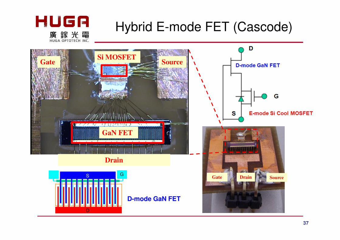
Hybrid E-mode FET (Cascode)
37
G
D
S G
D
S
Gate Source
Drain
Si MOSFET
GaN FET
Gate Drain Source
D-mode GaN FET

38
Hybrid E-mode FET (Cascode)
� � � � � � � �
�� � � � � � �� � � � � � � � � �
� � � � � � � � � � � � � � � � � � � � � � ! ! � � � " � # ! � � � � � � � $
%& � � & � � �� � ' � � %� � � � ( � ) * * ) * * %
+ & � � � � � � ! � & � � � � � � � , � , � -
+ & � � � � � � � � � � & � � � � � � � , * * . � � -
/ & � � � � � � � ' � & � � �� � ' � � � � �/ � ! ! � � � ' � * 0 , � * 0 ) 1
%2 / 2 � � 3 � � # � � 4 � � � � ( � � � 5 � � * -$ 67 * * ) ) * %
%� � � " � ! " � � � � %� � � � ( � 6� % 8 %
� ! ! � ( ! 9 � ( � :; * , ) ) *
< ( � � � � � � � � � � � � " � ( � : 8* � � �
� / � 4 � ! � � / � ' � 4 � � � � � � . * , � * � !
< / � 4 � ! � � / � ' � 4 � � � � " � ( � , � 0 � ) 8* � � �
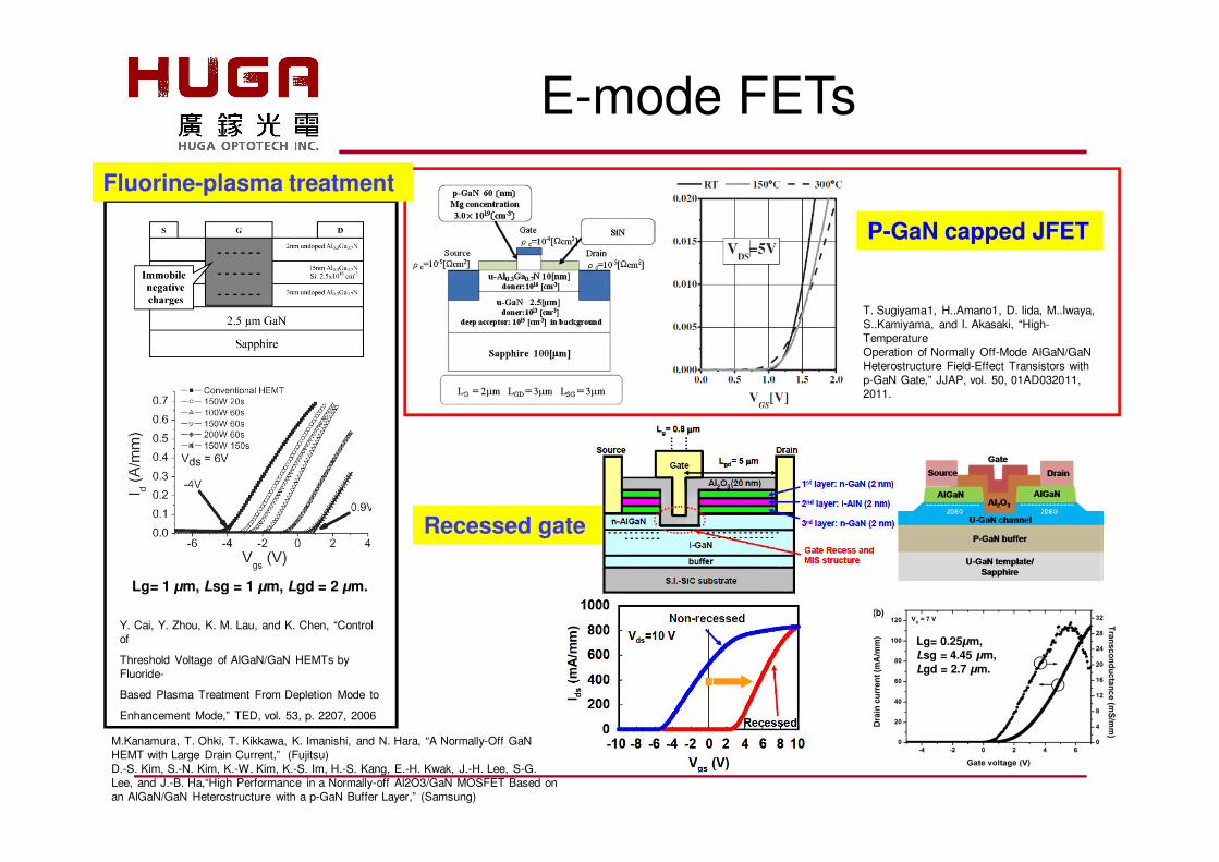
Y. Cai, Y. Zhou, K. M. Lau, and K. Chen, “Control of
Threshold Voltage of AlGaN/GaN HEMTs by Fluoride-
Based Plasma Treatment From Depletion Mode to
Enhancement Mode,” TED, vol. 53, p. 2207, 2006
Lg= 1 µm, Lsg = 1 µm, Lgd = 2 µm.
T. Sugiyama1, H..Amano1, D. Iida, M..Iwaya, S..Kamiyama, and I. Akasaki, “High-Temperature Operation of Normally Off-Mode AlGaN/GaNHeterostructure Field-Effect Transistors with p-GaN Gate,” JJAP, vol. 50, 01AD032011, 2011.
M.Kanamura, T. Ohki, T. Kikkawa, K. Imanishi, and N. Hara, “A Normally-Off GaNHEMT with Large Drain Current,” (Fujitsu)D.-S. Kim, S.-N. Kim, K.-W. Kim, K.-S. Im, H.-S. Kang, E.-H. Kwak, J.-H. Lee, S-G.Lee, and J.-B. Ha,“High Performance in a Normally-off Al2O3/GaN MOSFET Based on an AlGaN/GaN Heterostructure with a p-GaN Buffer Layer,” (Samsung)
Recessed gate
P-GaN capped JFET
Fluorine-plasma treatment
Lg= 0.25µm, Lsg = 4.45 µm, Lgd = 2.7 µm.
E-mode FETs
40
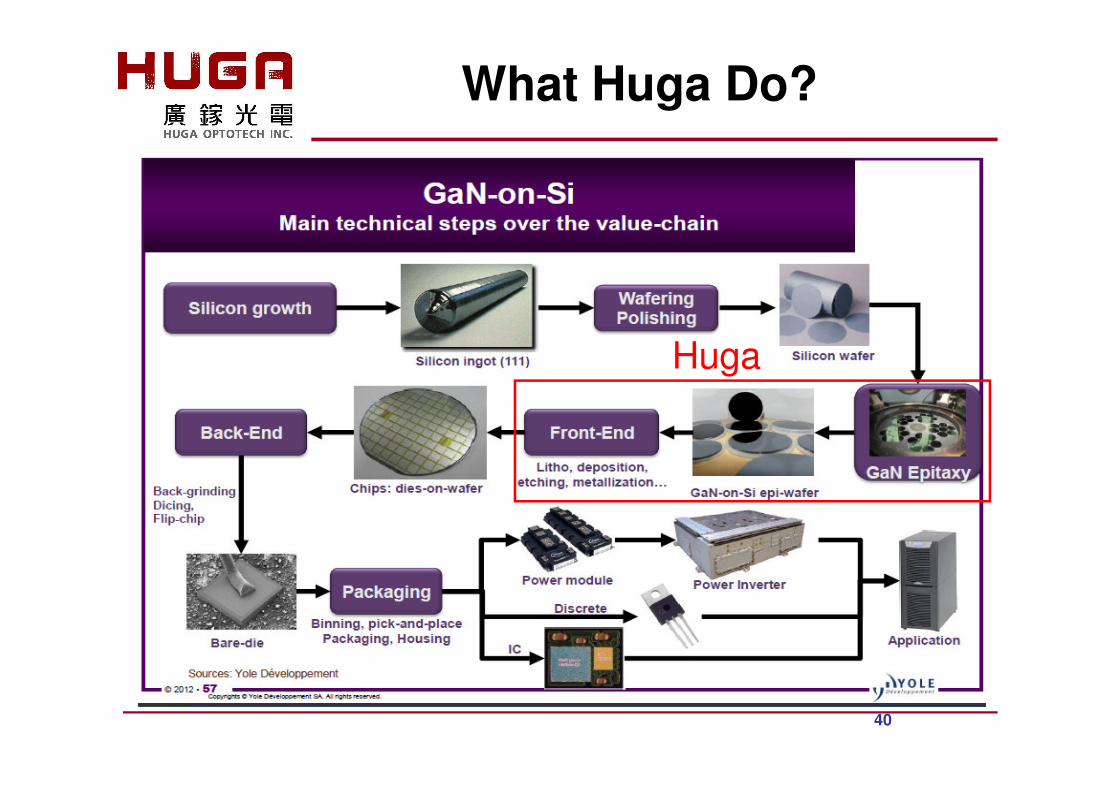
What Huga Do?
Huga
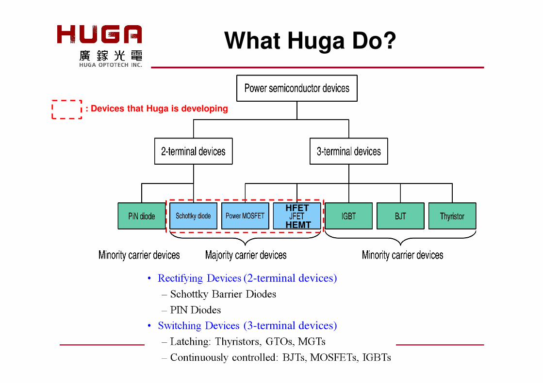
41
(2-terminal devices)
(3-terminal devices)
HFET
HEMT
: Devices that Huga is developing
What Huga Do?

Huga’s 6” GaN-on-Si Device Wafer
D-mode HFETSBD
IF = 8 A ( @ VF �2 V)VR = 6 0 0 V
ID = 1 0 ~ 1 2 AVD ( o f f -s t a t e ) = 6 0 0 V
43
Summary
• GaN is promising material for power device application. GaN-on-Si solution is an excellent option for balancing the requirement of performance and cost.
• Performance of GaN-on-Si power devices is similar to that of SiC power devices and much better than that of Si power devices. Plus, cost of GaN-on-Si power devices is in between.
• Though 600V GaN-on-Si power device products started appearing in the market recently, I believe it will take some time to have end users willing to widely apply them into various modules/systems.

44
Thank you !
���������������� � � � �� � � �� � � �� � � �
� � � �
� � � � � � � � � � � � � � � � � � �� � � � � � � � � � � � � � � � � � �� � � � � � � � � � � � � � � � � � �� � � � � � � � � � � � � � � � � � �