Embed Size (px)
Citation preview

July, August, September 2013 Page 1 The Simulation Standard
Engineered Excellence A Journal for Process and Device Engineers
INSIDE2D IBC-SHJ Solar Cell Simulation and Optimization ...................................................12Anode Shorts Layout Dependence of Bi-mode IGBT (BiGT) On-state Characteristics..................15Hints, Tips and Solutions ..........................................18
Continued on page 2 ...
Volume 23, Number 3, July, August, September 2013
Validation of the model has been carried out in Atlas and Victory Device based on [1,2] and simulation results for an AlGaN/GaN structure as shown in Figure 1 and 2.
Mobility and impact Ionization models are also GaN-specifi c. You can use a composition and temperature dependent low fi eld model by specifying the FMCT.N and FMCT.P in the MOBILITY statement. FMCT stands for Farahmand Modifi ed Caughey Thomas. This model was the result
State of the Art 2D and 3D Process and Device Simulation of GaN-Based Devices
IntroductionSilicon has long been the semiconductor of choice for high-voltage power electronics applications. However, wide-bandgap semiconductors such as SiC and GaN have begun to attract attention because they are pro-jected to have much better performance than silicon. In comparison with silicon, wide-bandgap semiconductors offer a lower intrinsic carrier concentration, a higher electric breakdown fi eld, a higher thermal conductivity, and a faster saturated electron drift velocity.
Simulating GaN devices is more challenging compared to Silicon. Indeed very low intrinsic concentration com-bined with high doping values is usually detrimental to convergence. Since GaN is as wide a band gap material as SiC, we thus use the same simulation approach used for SiC and describe in details in http://www.silvaco.com/tech_lib_TCAD/simulationstandard/2013/jan_feb_mar/a1/state_of_the_art_3D_SiC_Process_and_device_simu-lation_a1.html
In the following paragraphs we will fi rst review the physics involved and needed for accurate simulation of GaN based devices. We will then illustrate our simula-tion fl ow with few examples.
Physical Model RequirementsIt is well known that AlGaN/GaN based HFETs exhibit two-dimensional electron gases (2DEG) contributing to outstanding performance without having to add doping to the structure. This 2DEG results from the also well- known combination of spontaneous (zero strain) and piezoelec-tric (strained) polarization. The computation of the 2DEG due to the polarization effect is performed automatically during the simulation thanks to our built-in model. From a practical point of view it means that the user do not have to specify any charges at a specifi c interface location between materials when changing the thicknesses or the composition fraction.
Figure 1. comparison of the built-in piezoelectric model between Atlas and Victory Device.

The Simulation Standard Page 2 July, August, September 2013
of fi tting a Caughey Thomas like model to Monte Carlo data [3]. You can also choose to model low fi eld mobility as a function of doping and temperature following the work of Albrecht et.al [4] by specifying ALBRCT on the MODEL statement or ALBRCT.N or ALBRCT.P or both on the MOBILITY statement for separate control over electrons and holes. You can fi nally select the nitride-spe-cifi c high fi eld dependent mobility model by specifying GANSAT.N and GANSAT.P on the MOBILITY statement. This model [3] is based on a fi t to Monte Carlo data for bulk nitride and exhibits negative differential mobility as shown in Figure 3.
As far as Impact Ionization is concerned, using the tabu-lar Selberherr model, we provide build-in tabular rep-resentations of results from several recent publications. We provide convenient access using different key words on the IMPACT statement. Figure 4 shows a comparison of the various tabular ionization rate models against the default models.
Performance of GaN devices can be altered by the pres-ence of defects (traps and intraps) and also by self heat-ing. It is thus important to take these effects into ac-count during simulation. Our simulators allow 2D and 3D simulation of self heating effects. Models include heat generation, heat fl ow, lattice heating, heat sinks, and effects of local temperature on physical constants. Thermal and electrical physical effects are coupled through self-consistent calculations. IV characteristics are not always reproductible as a result of deep traps in the nitride material. A deep trap may be regarded as an impurity or crystal defect that captures a mobile charge carrier and keeps it strongly localized in the neighbor-hood of the trapping center. Deep traps can produce current collapse, a distortion of the device current-volt-age (I-V) characteristic that is of particular concern be-cause it ultimately limits the output power of the device. Discrete and continuous Traps and Interface traps are available in Atlas and Victory so that these effects can be taken into account.
The main concept of GaN-based power devices is to use epitaxial strain to create 2DEG. As mentioned above we provide a built-in model for that. On top of that, this built-in model also supports dependency on a loaded strain tensor resulting for example from a deposited stress-liner made of nitride on top of the AlGaN/GAN layers. The “intrinsic” stress resulting from this nitride layer is computed using Victory Stress and can be direct-ly loaded in Atlas or Victory Device.
ApplicationsIn this section we will review and show 2D and 3D simu-lations of different type of structures. We will compare simulation results with experiments and show different type of simulations including DC, Transient, AC and large signal.
Figure 2. Sheet carrier concentration versus alloy composition and thicknesses.
Figure 3. Velocity-fi eld curves for pure GaN for various low-fi eld.
Figure 4. Comparison of electron ionization rates as a function of reciprocal fi eld with extrapolation enabled.

July, August, September 2013 Page 3 The Simulation Standard
A Normally-off GaN MISFET with High Vth uniformityThis example demonstrates the simulation of a GaN met-al-insulator-semiconductor fi eld effect transistor (MIS-FET) with Piezo Neutralization Technique (PNT) [5].
The fi rst feature of the PNT structure is an AlGaN buffer layer to realize a normally-off operation. The polariza-tion charges at the interface between the AlGaN buffer and the GaN channel act as virtual p-type doping and contribute to simultaneously increase Vt and charge den-sity in the channel. The band diagram and IdVg shown in Figure 5 and in Figure 6 respectively demonstrate the impact of the buffer Al-concentration on the electron-channel energy beneath the gate and Vth respectively.
The second feature is an Al0.07Ga0.93N PNT layer having an identical Al composition with the buffer layer to realize high Vth uniformity. Since PNT and buffer layers have an identical Al mole fraction, the polarization charges formed between these layers are completely canceled, and hence a fl at band condition occurs throughout the PNT layer.
Vth dependence on the AlGaN layer thickness under the gate electrode was simulated. For the GaN FETs with the PNT structure, the Vth is not affected by the variation of AlGaN thickness whereas it varies for the conventional Al0.15Ga0.85N/GaN single heterojunction FETs as as shown in Figure 7.
The last feature is the second supply layer at the region out-side the gate electrode to reduce on-resistance of the GaN FET. Since the second supply layer is consisted of AlGaN with higher Al composition than that for the fi rst supply layer, a large amount of 2DEG is produced both in the chan-nel layer and the PNT layer as shown in Figure 8.
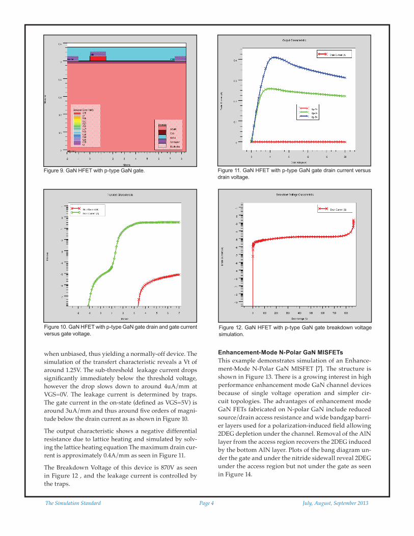
A Normally-off GaN HFET with p-type GaN gateThis example demonstrates simulation of a GaN HFET with p-type GaN gate [6] shown in Figure 9.
While a Schottky-type metal on the AlGaN barrier acts as a gate for normally-on HEMTs, a p-type doped semi-conductor gate is able to deplete the transistor channel
Figure 5. Conduction band energy under the gate versus AlGaN x composition.
Figure 6. IdVg curves as a function of AlGaN x composition. Figure 8. Polarization charge concentration outside the gate region in the PNT structure.
Figure 7. IdVg curves from conventional and PNT structures with different AlGaN thickness.
The Simulation Standard Page 4 July, August, September 2013
when unbiased, thus yielding a normally-off device. The simulation of the transfert characteristic reveals a Vt of around 1.25V. The sub-threshold leakage current drops signifi cantly immediately below the threshold voltage, however the drop slows down to around 4uA/mm at VGS=0V. The leakage current is determined by traps. The gate current in the on-state (defi ned as VGS=5V) is around 3uA/mm and thus around fi ve orders of magni-tude below the drain current as as shown in Figure 10.
The output characteristic shows a negative differential resistance due to lattice heating and simulated by solv-ing the lattice heating equation The maximum drain cur-rent is approximately 0.4A/mm as seen in Figure 11.
The Breakdown Voltage of this device is 870V as seen in Figure 12 , and the leakage current is controlled by the traps.
Enhancement-Mode N-Polar GaN MISFETsThis example demonstrates simulation of an Enhance-ment-Mode N-Polar GaN MISFET [7]. The structure is shown in Figure 13. There is a growing interest in high performance enhancement mode GaN channel devices because of single voltage operation and simpler cir-cuit topologies. The advantages of enhancement mode GaN FETs fabricated on N-polar GaN include reduced source/drain access resistance and wide bandgap barri-er layers used for a polarization-induced fi eld allowing 2DEG depletion under the channel. Removal of the AlN layer from the access region recovers the 2DEG induced by the bottom AlN layer. Plots of the bang diagram un-der the gate and under the nitride sidewall reveal 2DEG under the access region but not under the gate as seen in Figure 14.
Figure 10. GaN HFET with p-type GaN gate drain and gate current versus gate voltage.
Figure 11. GaN HFET with p-type GaN gate drain current versus drain voltage.
Figure 12. GaN HFET with p-type GaN gate breakdown voltage simulation.
Figure 9. GaN HFET with p-type GaN gate.

July, August, September 2013 Page 5 The Simulation Standard
The simulation of the transfert characteristic reveals a Vt of around 1V and a maximum Ids of around 0.7A/mm at Vgs=5V as seen in Figure 15. Electron injection from the channel to the gate is limited
by the AlGaN/GaN heterojunction. As a consequence no current offset is observed at zero drain since gate current is very low. This device exhibit a threshold voltage around 1V, a maximum drain current at Vd=10V and Vg=5V of 200mA/mm and a breakdown voltage of 640V as as shown in Figure 17, Figure 18 and Figure 19 respectively.
Figure 13. Enhancement-Mode N-Polar GaN MISFETs.
Figure 14. Bang diagram under the gate, under the nitride sidewall and under the drain regions.
Figure 15. Drain current versus gate voltage.
Normally-off AlGaN/GaN Transistor with Conductivity ModulationThis example demonstrates simulation of a normally-off AlGaN/GaN transistor with conductivity modulation resulting from hole injection from a p-AlGaN gate to the AlGaN/GaN heterojunction [8]. The p-AlGaN gate allows normally-off operation.
When the gate voltage increases and reaches the built-in pn junction voltage at the gate (around 3.5V) holes inject into the channel and generate the equal number of elec-trons increasing the 2DEG. Electrons with high mobility will reach the drain under the effect of the electric fi eld whereas the holes will stay since their mobility is much lower than the electron. The current is thus modulated by the number of holes injected. It is also interesting to notice that this device exhibits a double peak in the transconductance curve, a second proof of hole injection as as shown in Figure 16.
Figure 16. Transconductance versus gate voltage.

The Simulation Standard Page 6 July, August, September 2013
Fe Bulk Doping Related Current Collapse PhenomenonThis example demonstrates simulation of the “Current Collapse” and “Current Recovery” phenomenon result-ing from population and de-population of Intentional Iron (Fe) Doping Traps under the gate of a GaN FET as a result of Gate to Drain Electric Fields.
Many publications suggest that unintentional surface traps are the main cause of the GaN current collapse phenomenon. In this example, we show that some-times this is not actually the case. Current collapse in this device is mostly caused by intentional iron dop-ing, whose main purpose is to create a semi-insulating buried layer to reduce the buried layer source-to-drain leakage path.
The device structure in this example is based on [9].
Substrate leakage current is controlled by a graduated concentration of deep level iron acceptor traps located 1eV below the conduction band edge.
The device is first biased with 0v on the gate and 5v on the drain. After a mili-second at this bias, the device is field stressed for only one further milli-second at 25v on the drain and -4v on the gate as seen in Figure 20. After this short bias stress, the device was returned to its origi-nal bias of 0v on the gate and 5 volts on the drain. After only one milli-second of bias stress, the drain current is significantly reduced demonstrating the current collapse phenomenon as seen in Figure 21.
Figure 18. Drain current versus drain voltage.
Figure 19. Breakdown voltage characteristic.
Figure 20. Gate and drain voltage biases.
Figure 21. Current collapse simulation result.
Figure 17. Drain current versus gate voltage.

July, August, September 2013 Page 7 The Simulation Standard
A comparison structure file plot of the pre and post-stress ionized Fe trap density shows that the cause of the current collapse is actually the change in charge state of the Fe doping deep in the substrate under the gate, and also on the drain side between the gate and drain con-tacts as seen in Figure 22.
stress distributions via the stress-liner made of nitride as shown in Figure 24 and Figure 25. Note that the stressor in this example is used to illustrate strain polarization on top of piezo and spontaneous polarization.
Figure 22. Pre and post stress ionized Fe trap density.
Figure 23. Device recovery simulation.
Figure 24. 3D AlGaN/GaN HEMT.
Figure 25. Strain XX generated by a stress-liner made of nitride.
Figure 26. Drain current versus gate voltage for ore and post-stres device.
For completeness, the unstressed bias remained on the device until the traps became de-populated with elec-trons and the drain current returned to its original val-ue. Interestingly, it takes over one week for the device to recover. (6e5 seconds) as seen in Figure 23. This very long recovery time may be incorrectly interpreted as de-vice degradation from field-induced traps which is an irreversible effect resulting from electric field-induced reverse piezo-electric stress.
2-6 3D AlGaN/GaN HEMT Including Intrinsic Stress EffectThe device under consideration is a 3D AlGaN/GaN HEMT shown in Figure 24. 3D stress distribution is simulated by Victory Stress. This example produces

The Simulation Standard Page 8 July, August, September 2013
After the initial solution is obtained, the drain voltage is ramped to 1 V, then the IdVg characteristic is extracted from Vg=-8 to Vg=1.0 V as seen in Figure 26. The effect of strain is seen on IdVg. Overlay of 2D simulation results with 3D simulation results obtained with width=1 vali-dates our 3D implementation.
Influence of the Gate to Drain distance on the break-down voltageThis example demonstrates the influence of the gate-to-drain distance on the breakdown voltage with and with-out silicon substrate [10]
The structure consists of 20nm AlGaN with xcomp=0.2 and 1um GaN buffer layer as as shown in Figure 27. Do-nor and acceptor traps are included in the simulation. Gaussian profile acceptor traps are used with a peak concentration close to the bottom of the buffer layer to mimic the fact that the material quality improves toward the surface of the device.
Donor Interface traps at the AlGaN/Nitride interface and acceptor interface traps at the GaN/Silicon interface are also included during the simulation.
Forward characteristic simulation reveals a threshold voltage of around -2V. Slow transient simulation is used to simulate the breakdown voltage curve.
The deck is parametrized so that we can vary the dis-tance between the gate and drain (LGD). DeckBuild DoE capability is used to automate simulations of BV versus LGD with and without substrate.
We can observe in Figure 28 an almost linear increase of BV versus LGD when silicon substrate is not present. An increase of the gate current is observed in Figure 29 near breakdown, and the value is of the same order as the drain current. This result indicates that BV is defined by an avalanche phenomenon between the gate and the drain as shown in Figure 30.
BV does not depend significantly on LGD when a silicon substrate is present due to charge accumulation at the GaN/Silicon interface, related to the presence of inter-face traps, which screen the electric field.
Figure 27. AlGaN/GaN HEMT with and without Silicon substrate.
Figure 28. BV versus LGD with and without silicon substrate Fig-ure 29 Drain and gate current versus drain voltage.
Figure 29. Drain and gate current versus drain voltage.
Figure 30. Potential distribution as a function of LGD distance.
July, August, September 2013 Page 9 The Simulation Standard
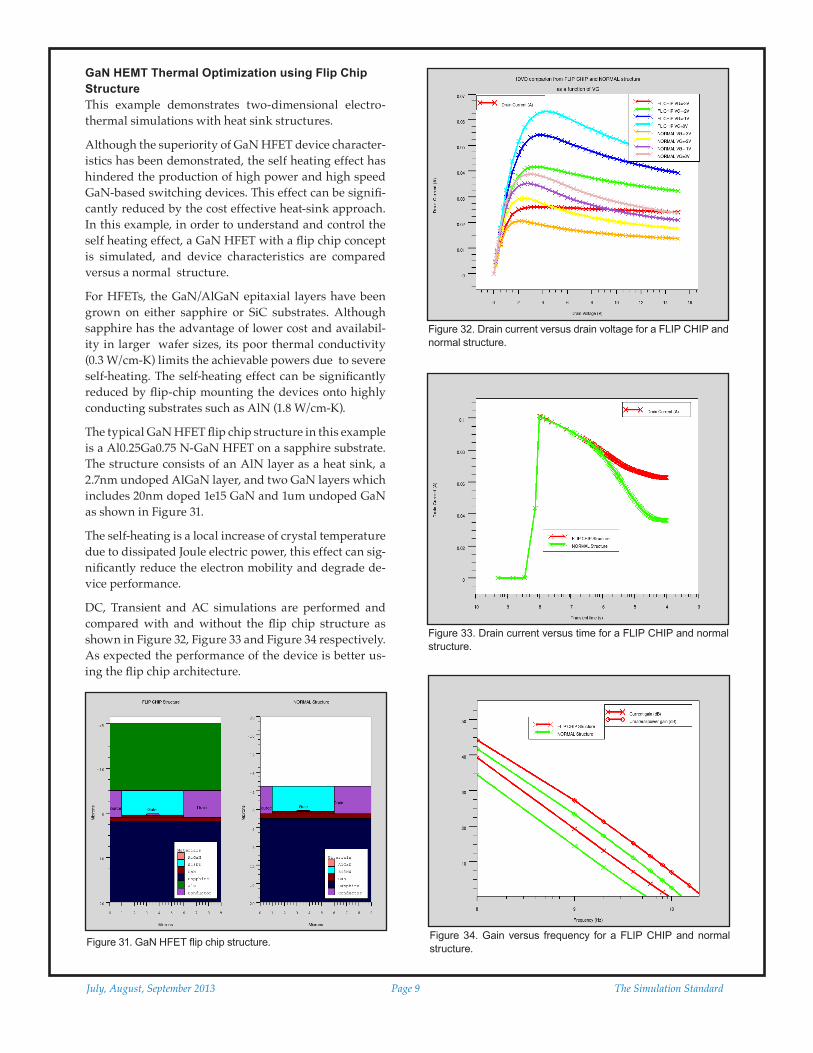
GaN HEMT Thermal Optimization using Flip Chip Structure This example demonstrates two-dimensional electro-thermal simulations with heat sink structures.
Although the superiority of GaN HFET device character-istics has been demonstrated, the self heating effect has hindered the production of high power and high speed GaN-based switching devices. This effect can be signifi-cantly reduced by the cost effective heat-sink approach. In this example, in order to understand and control the self heating effect, a GaN HFET with a flip chip concept is simulated, and device characteristics are compared versus a normal structure.
For HFETs, the GaN/AlGaN epitaxial layers have been grown on either sapphire or SiC substrates. Although sapphire has the advantage of lower cost and availabil-ity in larger wafer sizes, its poor thermal conductivity (0.3 W/cm-K) limits the achievable powers due to severe self-heating. The self-heating effect can be significantly reduced by flip-chip mounting the devices onto highly conducting substrates such as AlN (1.8 W/cm-K).
The typical GaN HFET flip chip structure in this example is a Al0.25Ga0.75 N-GaN HFET on a sapphire substrate. The structure consists of an AlN layer as a heat sink, a 2.7nm undoped AlGaN layer, and two GaN layers which includes 20nm doped 1e15 GaN and 1um undoped GaN as shown in Figure 31.
The self-heating is a local increase of crystal temperature due to dissipated Joule electric power, this effect can sig-nificantly reduce the electron mobility and degrade de-vice performance.
DC, Transient and AC simulations are performed and compared with and without the flip chip structure as shown in Figure 32, Figure 33 and Figure 34 respectively. As expected the performance of the device is better us-ing the flip chip architecture.
Figure 31. GaN HFET flip chip structure.
Figure 32. Drain current versus drain voltage for a FLIP CHIP and normal structure.
Figure 33. Drain current versus time for a FLIP CHIP and normal structure.
Figure 34. Gain versus frequency for a FLIP CHIP and normal structure.

The Simulation Standard Page 10 July, August, September 2013
Large Signal Output Power Analysis This example describes how to simulate typical 10 GHz large-signal measured performance quantities related to power output, such as power out versus power as shown in Figure 35, power gain as shown in Figure 36 and am-plifier efficiency as shown in Figure 37 as the device is over-driven into high distortion. The example also plots in Figure 38 the output signal shape versus time for each of the ten input signal levels simulated.
The structure under test is shown in Figure 39.
Ten large signal input amplitudes are defined. Each of these waveforms are applied to the gate in order of in-creasing amplitude. After each waveform simulation is complete, a number of large signal parameters are calcu-lated. The peak input and output voltages are extracted, followed by the exact times at which these peak volt-ages occurred. Then the input and output currents are extracted at the same times as the peak voltages occur. It is important to extract the currents at the same time as the peak voltages in order to take account of the phase between current and voltage, so that the correct power values can be calculated.
Figure 36. Power gain versus power out.
Figure 37. Power Output Efficiency verus Power out.
Figure 38. Drain and gate voltage large signal.
Figure 39. Structure under test.
Figure 35. Power out versus power in.

July, August, September 2013 Page 11 The Simulation Standard
ConclusionGaN is a very promising material for high power switch-ing applications. However, development cost is becom-ing a serious concern for GaN manufacturers. This is why TCAD is so important in order to reduce cost and help optimize device performance.
Silvaco’s Process and Device solutions have all the capa-bilities ( i.e. state of the art mesh, discretization, solvers and physcial models) that we think are essential to accu-rately simulate GaN based devices in 2D and 3D.
References[1] Naiqian Zhang, “High voltage GaN HEMTs with low on-resitance
for switching applications”, dissertation, UCSB september 2002
[2] O.Ambacher et al. “Two-dimensionalelectron gases Induced by spontaneous and piezoelectric polarization charges in N- and Ga-face AlGaN/Gan Heterostructures” J. Appl. Phys. Vol 85, 3222(1999)
[3] Farahmand, M., et al, “Electron Transport Characteristics of GaN for high temperature device modeling” J. Appl. Phys. Vol 83,4777-4781 (1999)
[4] Albrecht, J.D. et al, “Monte Carlo simulation of Electron Transport in the III-Nitride Wurtzite Phase Materials Sustems: binaries and Ternaries” IEEE Trans. Electron Device Vol,48, NO. 3 March 2001
[5] Ota, K. et. al. “A Normally-off GaN FET with High Threshold Volt-age Uniformity Using A Novel Piezo Neutralization Technique”, IEDM 2009, pp. 153-156.
[6] O. Hilt, A. Knauer, F. Brunner, E. Bahat-Treidel and J. W√ºrfl “Nor-mally-off AlGaN/GaN HEFT with p-type GaN Gate and AlGaN Buffer” Ferdinand-Braun-Institut, Leibniz Institut fuer Hoechstfre-quenztechnik Gustav-Kirchhoff-Strasse 4, 12489 Berlin, Germany. Proceedings of The 22nd International Symposium on Power Semi-conductor Devices & ICs, Hiroshima.
[7] Uttam Singisetti, et al., “Enhancement-Mode N -Polar GaN MIS-FETs With Self_Aligned Source/Drain Regrowth” IEEE Electron Device Letters. Vol,32, NO. 2 feb 2011.
[8] Yasuhiro Uemoto “A Normally-off AlGaN/GaN Transistor with Ron=2.6mOhmcm2 and BVds=640V Using Conductivity Modula-tion” published at IEDM 2006.
[9] Daniel Balaz from his PhD Thesis from University of Glasgow in 2011 entitled “Current collapse and device degradation in AlGaN/GaN heterostructure field effect transistors”.
[10] Experimental and simulation study of breakdown voltage enhance-ment of AlGaN/gaN heterostructures by Si substrate removal. D.Visalli et al Apl. Phys. Lett. 97, 113501 2010.

The Simulation Standard Page 12 July, August, September 2013
2D IBC-SHJ Solar Cell Simulation and Optimization
Figure 1. IBC-SHJ solar cell elementary structure.
IntroductionInterdigitated back contact silicon heterojunction (IBC-SHJ) combines the advantages of interdigitated back contact (IBC) and silicon heterojunction (SHJ) solar cells. Having all the contacts at the back of the cell eliminates contact shading, leading to a higher short-circuit current (JSC). Being a heterojunction device, IBC-SHJ also has the potential of higher open circuit voltage (VOC) due to the better surface passivation of the deposited amorphous sil-icon (a-Si) layer. The low temperature deposition, instead of high temperature diffusion, decreases thermal stress, which is the trend of future silicon solar cells. Rear surface passivation by deposited intrinsic amorphous silicon (a-Si) buffer layer in IBC-SHJ solar cells signifi cantly improves open circuit voltage (VOC) and short circuit current (JSC) but can lead to very low fi ll factor (FF) with an “S” shape J-V curve. In this paper, methods to optimize IBC-SHJ so-lar cell with improved FF are discussed and guided by two-dimensional numerical simulation. The modeling of the IBC-SHJ solar cell requires device simulation software operating in two dimensions and incorporating amor-phous silicon. To study this innovative structure, we use ATLAS two-dimensional (2-D) device simulation software that provides accurate bulk and interface defects needed to model amorphous silicon. We fi rst present the geomet-rical structure of the solar cell, then review the general framework of the simulation by specifying the different physical models, and fi nally examine the simulation re-sults in order to determine the important parameters to achieve high effi ciency.
Device StructureBack contact cells differ from conventional structures in that all contacts are on the back side (not illuminated side) of the cell. The front surface is subject to illumination. On the rear side, we have an interdigitated structure of hy-drogenated amorphous silicon layers alternately n-type and p-type to play the role of emitter or back surface fi eld (BSF) according to the c-Si substrate doping. We used an n-type c-Si substrate in this Device. The emitter (p-stripe) and the BSF (n-stripe) are covered by metal contacts. An intrinsic a-Si buffer layer was deposited over the entire rear surface of the IBC-SHJ solar cell. The IBC-SHJ solar cell presents a periodic structure. The periodicity of the structure allows us to use an elementary structure, shown in Figure 1, that will serve as a basis for optimizing the performance of this type of cell. The geometrical and ma-terial parameters of the simulated structure were chosen according to [1].
Physical Models The simulation is based on the solution of three govern-ing semiconductor equations: Poisson’s equation, electron and hole continuity equations. Fermi statistic was used for carriers with drift-diffusion combined with Bohm Quantum Potential for quantum correction. Fermi mod-el and Recombination models (i.e srh, auger and surface recombination) were also included into the simulation. For a-Si layers, critical parameters like band gap, doping and defect distribution are defi ned in the input deck. The critical parameters for accurate simulation are energy dis-tribution of the exponential band tails, and the Gaussian distribution of the mid-gap trap states. They were chosen according to reference [1] and shown in Figure 2. For c-Si/a-Si interfaces at the back surface a thermionic emis-sion model was used. For even more realistic modeling of this interface we have introduced defect states at the hetero-interface by putting a very thin defective layer of c-Si [2]. An AM1.5G solar spectrum is used for the optical generation to simulate the J-V curve under standard one-sun illumination conditions. A Sopra database is used for a-Si index of refraction.
To properly simulate the behavior of the structure, it is essential to apply an adapted mesh. A mesh as thin as possible applied to the whole structure ensures good accuracy of calculations but requires greater computa-tion time to simulate the behavior of this structure. It is therefore necessary to fi nd a compromise between com-putational time and accuracy of the calculation. To reach this compromise, we applied a fi ne mesh only in areas where changes in physical quantities are important and a coarse mesh in areas where these quantities are quasi

July, August, September 2013 Page 13 The Simulation Standard
Figure 2. Density of States (DOS) in a-Si material.
Figure 3. Mesh of the elementary IBC-SHJ solar cell. Figure 4. IV curves as a function of a-Si thickness.
static. Thus, the mesh is refi ned in the critical areas that are the front surface (strong absorption), the c-Si/a-Si:H hetero-interfaces and the areas around frontiers of the various layers in which the variations of physical quan-tities are important. In the middle of the c-Si substrate, a coarse mesh is used as the physical quantities do not vary signifi cantly. Figure 3 represents the mesh used to simulate IBC-SHJ solar cell.
Simulation Results A complete parametrized input deck, including geom-etry and mesh, was created not only to optimize simula-tion time and accuracy but also for solar cell optimiza-tion purposes. This input deck was used in DBinternal to vary different parameters in order to optimize the solar cell effi ciency. DBINTERNAL is a simple but powerful DECKBUILD tool that allows you to create a Design Of Experiments (DOE) from a pair of input fi les. Amongst other things, you can create corner models for process
parameters or device characteristics or both. Any param-eters that are to be used as variables must be specifi ed as set statements in a template fi le. Any results of interest should be calculated using extract statements. The DOE is specifi ed with simple sweep statements in a separate design fi le. The sweep statement defi nes which variables are required in the DOE, and the range of values these variables are to take. The parameter values and the re-sults of each simulation can be stored in a fi le that can be viewed in TonyPlot or used as a database for input to a statistical analysis tool such as SPAYN. We have chosen 4 parameters to optimize effi ciency. These parameters are intrinsic a-Si thickness, n-stripe and p-strip width and gap width.
It was experimentally observed that an intrinsic a-Si layer increases Voc and Jsc but also decreases FF and leads to a “S” shape IV curve. Simulation results, shown in Figure 4, confi rm the reduction of FF and “S” shape IV curve.

The Simulation Standard Page 14 July, August, September 2013
Figure 5. IBC-SHJ solar cell Key figure of merits as a function of a-Si thickness.
Figure 6. IBC-SHJ solar cell Key figure of merits as a function of n-stripe width.
Figure 7. IBC-SHJ solar cell Key figure of merits as a function of gap width.
Figure 8. IBC-SHJ solar cell key figure of merits as a function of p-stripe width.
The results of the DoE are shown in Figures 5, 6, 7 and 8. Figure 5 shows an increase of Voc when the thickness of the intrinsic a-Si layer increases as reported in [3], leading to an optimum efficiency of around 10nm for the intrinsic a-Si layer. n-stripe, p-stripe and gap width were also optimized. Figures 6 and 7 show that Jsc decreases when n-stripe width and gap width increases. As a consequence n-stripe and gap width have to be chosen as narrow as possible.
It is interesting to notice that Jsc increases and FF de-creases when p-stripe increases as shown in Figure 8. The different evolution of Jsc and FF leads to an optimum for the efficiency of around 1mm for p-stripe width.
Conclusion2D numerical simulations were performed in order to study and optimize IBC-SHJ solar cells. The impact of several geometrical parameters were studied and their impact was shown on the IBC-SHJ solar cell output char-acteristics. This gives the designer guidelines to achieve high efficiency IBD-SHJ solar cells.
References[1] M.Lu et al “Optimization of interdigital back contact silicon
solar cells by two-dimensional numerical simulation” IEEE 2009.
[2] D. Diouf, J.-P. Kleider, and C. Longeaud, “Two-Dimensional Simulations of interdigitated ack Contact Silicon Hetero-junctions Solar Cells”, Chapter 15 of the book “Physics and Technology of Amorphous-Crystalline Silicon Heterostruc-ture Solar Cells”, Springer 2011.
[3] D.Munos et al. INES-CEA, “Key features of highly efficient a-Si:Hc-Si heterojunction solar cells” 7th Workshop on the future Direction of Photovoltaics (by JSPS 175th commit-tee), march, 2011.

July, August, September 2013 Page 15 The Simulation Standard
Anode Shorts Layout Dependence of Bi-mode IGBT (BiGT) On-state Characteristics
Figure 1. The basic structure of a BiGT [2].
Reverse Conducting IGBT (RC-IGBT)A new class of high-voltage semiconductor devices, known as a reverse conducting IGBT (RC-IGBT), has emerged in recent years from research efforts to dimin-ish the usage of external anti-parallel free-wheeling di-ode chips for IGBT switching applications. The RC-IGBT device concept is based on the monolithic integration of a freewheeling diode into an IGBT chip. Hereby, an an-ti-parallel diode is formed through the embedment of an n+ region in an anode/collector region of the IGBT. Both the n+ region and the p+ anode are then shorted together by an anode/collector contact. Although the RC-IGBT has many advantages over the conventional IGBT, especially in terms of manufacturing cost, total chip size and reliability of power modules, it is detri-mental to the snapback effect at forward conduction of IGBT mode.
Snapback Effect in RC-IGBTIn the on-state IGBT mode of an RC-IGBT, when elec-trons flow from a cathode/emitter contact through an n-buffer region (or an n-drift region in case of a non-punch-through IGBT) to an n+ region at the anode/col-lector contact, they forward bias the p+-anode /n-buffer junction. On grounds of reflection symmetry, the voltage drop across the junction has its maximum value in the middle of the p+ anode region. Only after a sufficiently high voltage drop has built up in response to an increase in the collector current does the p+ anode start injecting holes into the n- drain drift region, with the result that the drift region becomes less resistive by conductivity modulation. An increase in hole levels in the drift region above the doping concentration eventually gives rise to a voltage snapback.
Bi-mode Insulated Gate Transistor (BiGT)The Bi-mode insulated gate transistor (BiGT) represents a further development of the RC-IGBT device concept, with the primary objective of alleviating the snapback effect in RC-IGBT. Recent research results have indicated that the snapback voltage in the RC-IGBT on-state char-acteristics decreases with the increase of the width of the p+ anode [1]. Accordingly, the BiGT device is built around the concept of incorporating an IGBT with a wide p+ anode, also referred to as pilot-IGBT, into the RC-IGBT structure as outlined in Figure 1.
Design Analysis and 3D Simulation with Victory Process and DeviceStudies in [3] have shown that, in the on-state of the BiGT, the anode shorts layout design of the RC-IGBT portion affects the conductivity modulation of the entire BiGT, and therefore its on-state behavior. They attribute the cause of this layout-dependent device performance to the lateral spread of the electron-hole plasma from the pilot-IGBT into the RC-IGBT and suggest a possibil-ity of snapback suppression by a radial layout design of anode shorts.
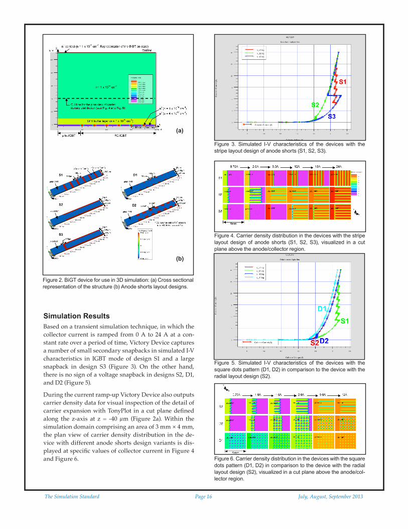
In order to verify the validity of the arguments and re-produce the results reported in [3], 3D device simula-tions with Victory Device have been performed in com-bination with process simulation with Victory Process. Figure 2 illustrates the simulation structure of the BiGT as well as the anode shorts layout designs under consid-eration.
It follows that there are two basic patterns for anode shorts layouts – stripes (designs S1, S2 and S3), with each having the same width of 100 µm but different orienta-tions relative to the pilot-IGBT boundary, and square dots (designs D1 and D2), with each having squares whose all four sides equal to 100 µm and 224 µm respectively.
In the simulation domain with an area of 0.5 mm × 4 mm, the BiGT assumes a 100 µm-thick drain drift region, together with a 10 µm-thick SPT n+ buffer layer on a 2.5 µm-thick anode/collector region. For simplicity, the MOS cells on the emitter side are modeled with a 1 µm-thick heavily doped n-type layer of silicon, given the conducting state of the BiGT in the IGBT mode.
The Simulation Standard Page 16 July, August, September 2013
Simulation ResultsBased on a transient simulation technique, in which the collector current is ramped from 0 A to 24 A at a con-stant rate over a period of time, Victory Device captures a number of small secondary snapbacks in simulated I-V characteristics in IGBT mode of design S1 and a large snapback in design S3 (Figure 3). On the other hand, there is no sign of a voltage snapback in designs S2, D1, and D2 (Figure 5).
During the current ramp-up Victory Device also outputs carrier density data for visual inspection of the detail of carrier expansion with TonyPlot in a cut plane defined along the z-axis at z = -40 µm (Figure 2a). Within the simulation domain comprising an area of 3 mm × 4 mm, the plan view of carrier density distribution in the de-vice with different anode shorts design variants is dis-played at specific values of collector current in Figure 4 and Figure 6.
Figure 2. BiGT device for use in 3D simulation: (a) Cross sectional representation of the structure (b) Anode shorts layout designs.
Figure 3. Simulated I-V characteristics of the devices with the stripe layout design of anode shorts (S1, S2, S3).
Figure 4. Carrier density distribution in the devices with the stripe layout design of anode shorts (S1, S2, S3), visualized in a cut plane above the anode/collector region.
Figure 5. Simulated I-V characteristics of the devices with the square dots pattern (D1, D2) in comparison to the device with the radial layout design (S2).
Figure 6. Carrier density distribution in the devices with the square dots pattern (D1, D2) in comparison to the device with the radial layout design (S2), visualized in a cut plane above the anode/col-lector region.
(a)
(b)

July, August, September 2013 Page 17 The Simulation Standard
Analysis of ResultsIn the case of design S1, injection from each 100 µm-wide anode segment occurs by progressive stages as the electron current flows perpendicularly through the p+ anode segments. This means that injection from each an-ode segment corresponds to each secondary snapback in the device with design S1.
By contrast, the radial configuration of anode segments in the S2 design enables the electrons from the pilot-IGBT to flow and forward bias the p+ anode/n-buffer junction along the entire stripe length. As a result, the portion of anode segments adjacent to the pilot-IGBT starts inject-ing carriers that later on spread smoothly and without causing a voltage snapback all over the entire device volume at a relatively low current, compared to the S1 design.
With regard to design S3, the orthogonally arranged an-ode segments are disconnected to the pilot-IGBT, so hole injection from the anode stripes triggers a voltage snap-back at a higher current than design S1. Nevertheless, after the onset of snapback the anode stripes of design S3 rapidly supply the entire device volume with plasma, which thus renders the I-V curve behavior of design S3 at high current levels identical with that of design S2.
As far as the square dots pattern is concerned, the transi-tion of the devices with the D1 and D2 designs into full conduction goes as smoothly as the case of radial layout design S2, except that the available anode segment area essentially determines the device IGBT mode on-state I-V characteristics. Figure 5 reveals that the radial stripe design S2 exhibits a slightly higher on-state voltage drop than the D1 design but incurs almost exactly the same conduction losses as design D2. This agrees well with the fact that the S2 design provides the entire device area with almost exactly the same plasma as design D2, as it can be seen in Figure 6.
ConclusionsVictory Process and Device proves to be capable of repro-ducing consistent simulation data with reference to [3]. It allows users to speed up the product design process and shorten the development timeline considerably.
References[1] M. Rahimo, J. Vobecky, C. Corvasce,“1700V Bi-Mode In-
sulated Gate Transistor (BIGT) on Thin Wafer Technology,” Proc. ISPS10, pp. 243-247, 2010.
[2] M. Rahimo, A. Kopta, U. Schlapbach, J. Vobecky, R. Sch-nell, S. Klaka, “The Bi-mode Insulated Gate Transistor (BiGT) A potential technology for higher power applica-tions,” Proc. ISPSD09, pp. 282-286, 2009.
[3] L. Storasta, M. Rahimo, M. Bellini, A. Kopta, U. R. Vemula-pati, and N. Kaminski,“The Radial Layout Design Concept for the Bi-mode Insulated Gate Transistor,” Proc. ISPSD11, pp. 56-59, 2011.

The Simulation Standard Page 18 July, August, September 2013
Hints, Tips and Solutions
Q: How can I compare the results of 2D and 3D break-down simulations with Hatakeyama’s impact ioniza-tion model for 4H-SiC based power devices?
A: In a 4H-SiC crystal, the stacking sequence of a Si-C bilayer plane extends along the crystallographic c-axis direction, also referred to as the <0001> direction (see Figure 1). With regard to crystallographic orientation, avalanche breakdown process in 4H-SiC uniquely fea-tures anisotropy of avalanche breakdown field, i.e., im-pact ionization coefficients.
Victory Device has an option of an anisotropic impact ionization model based on the work of Hatakeyama, et al. [2]. In Hatakeyama’s impact ionization model, the ion-ization coefficients are strong functions of the strength and orientation of the electric field relative to the optical c-axis of the crystal. The orientation in 3D space of the optical axis can be defined with the ZETA and THETA parameters on a MATERIAL statement, as depicted in Figure 2.
Hereby, the ZETA parameter specifies the angle that the optical axis makes with the positive y-axis. The hor-izontal angular distance, measured clockwise around the y-axis, from the positive x-axis to the orthogonal projection of the optical axis on the x-z plane, is deter-mined by the parameter THETA. By default the ZETA and THETA parameters are both set to zero, i.e., ZETA = THETA = 0 degrees, which implies the alignment of the <0001> direction of 4H-SiC with the y-axis.
In 2D device simulations, with the y-axes of the 2D struc-ture being conventionally taken along the depth into the wafer, the default settings for the ZETA and THETA pa-rameters ensure that the c-axis of the 4H-SiC crystal is normal to the wafer surface. This is in agreement with the fact that commercial 4H-SiC substrates are typically cut perpendicular to the c-axis. In the case of 3D simu-lations, however, the z-axis conventionally indicates the depth direction of the wafer from the surface. Hence, in order for 3D breakdown simulation results to be directly comparable with 2D ones, the <0001> crystal axis must be oriented such that it coincides with the z-axis. This can be achieved by setting ZETA = 90 degrees and THE-TA = 90 degrees, respectively.
Taken as an example, sicex11.in [3] compares the 2D and 3D breakdown simulation results computed with Hat-akeyama’s model. The device under simulation illustrat-ed in Figure 3 is a 4H-SiC power MOSFET with a trench gate structure, created by Victory Cell and simulated at a high precision level with Victory Device. The simula-tion setup is such that the optical axis corresponds to the height of both the 2D and 3D device structure. It is obvi-ous from Figure 4 that the simulated 2D and 3D break-down characteristics have turned out to be in excellent agreement with each other. Figure 1. 4H-SiC crystallographic directions [1].
Figure 2. Definition of optical axis.

July, August, September 2013 Page 19 The Simulation Standard
Call for QuestionsIf you have hints, tips, solutions or questions to contribute,
please contact our Applications and Support Department Phone: (408) 567-1000 Fax: (408) 496-6080
e-mail: [email protected]
Hints, Tips and Solutions ArchiveCheck our our Web Page to see more details of this example
plus an archive of previous Hints, Tips, and Solutionswww.silvaco.com
References
[1] http://www.semiconductorwafers.net/SiC-Crystallography--Impor-tant-Polytypes-and-Definitions.html
[2] Hatakeyama, T., J. Nishio, C. Ota, and T. Shinohe, “Physical Model-ing and Scaling Properties of 4H-SiC Power Devices,” Proc. SIS-PAD, Tokyo (2005): 171-174.
[3] http://www.silvaco.com/examples/tcad/section43/example11/in-dex.html
Figure 3. 2D (left) and 3D (right) 4H-SiC trench-gate power MOSFET.
Figure 4. Comparison of 2D and 3D breakdown characteristics of the 4H-SiC trench-gate power MOSFET.

The Simulation Standard Page 20 July, August, September 2013
Worldwide Offices: Silvaco Japan [email protected]
Silvaco [email protected]
Silvaco [email protected]
Silvaco [email protected]
Silvaco [email protected]
USA Headquarters:
Silvaco, Inc.4701 Patrick Henry Drive, Bldg. 2Santa Clara, CA 95054 USA
Phone: 408-567-1000Fax: 408-496-6080