Embed Size (px)
Citation preview

Choosing the Correct GaN-Based Power Device for YourFast Charger Design
©2021 Power Integrations, Inc. | power.com

Market Wants Smaller USB Fast Chargers with More Power
2©2021 Power Integrations | power.com
Bigger batteries (5G, bigger display…) need higher
power for faster charging
Number of electronic gadgets per user is growing
Smartphone, tablet, notebook, smart-watch,
wireless headphones…
Wide adoption of USB PD has created a new space
for ultra-compact and slim chargers
Adapter-free charging
USB A/C ports embedded in wall-sockets, power
strips, appliances and furniture
Requires small size and good thermals to support
high ambient temperature
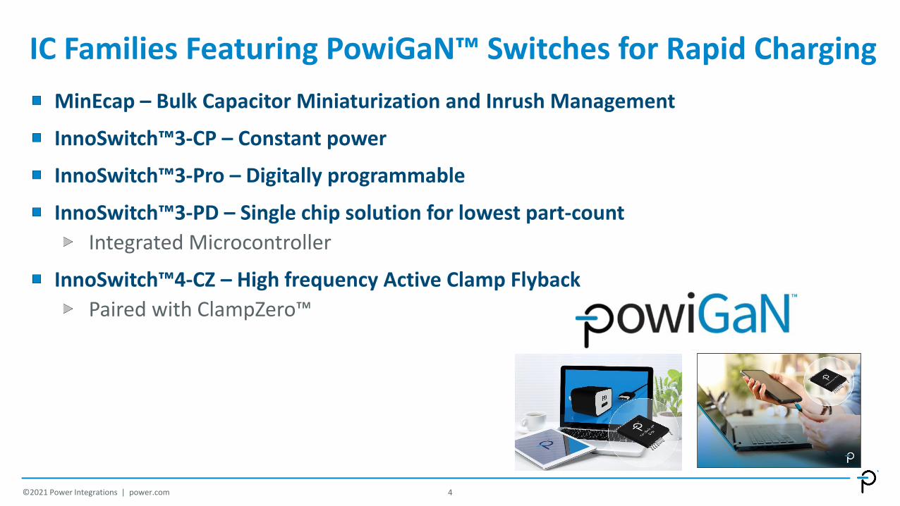
IC Families Featuring PowiGaN™ Switches for Rapid Charging
4
MinEcap – Bulk Capacitor Miniaturization and Inrush Management
InnoSwitch™3-CP – Constant power
InnoSwitch™3-Pro – Digitally programmable
InnoSwitch™3-PD – Single chip solution for lowest part-count
Integrated Microcontroller
InnoSwitch™4-CZ – High frequency Active Clamp Flyback
Paired with ClampZero™
Clamp
Zero
Clamp
Zero
©2021 Power Integrations | power.com
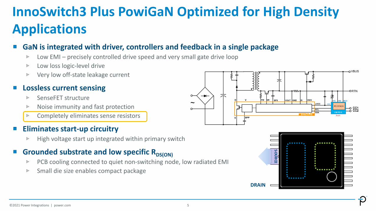
InnoSwitch3 Plus PowiGaN Optimized for High Density Applications
5
GaN is integrated with driver, controllers and feedback in a single package Low EMI – precisely controlled drive speed and very small gate drive loop
Low loss logic-level drive
Very low off-state leakage current
Lossless current sensing SenseFET structure
Noise immunity and fast protection
Completely eliminates sense resistors
Eliminates start-up circuitryHigh voltage start up integrated within primary switch
Grounded substrate and low specific RDS(ON)
PCB cooling connected to quiet non-switching node, low radiated EMI
Small die size enables compact package
DRAIN
©2021 Power Integrations | power.com

Advantages of InnoSwitch3
©2021 Power Integrations | power.com
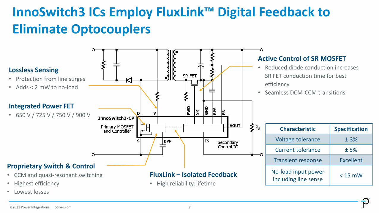
InnoSwitch3 ICs Employ FluxLink™ Digital Feedback to Eliminate Optocouplers
7
Integrated Power FET• 650 V / 725 V / 750 V / 900 V
Proprietary Switch & Control• CCM and quasi-resonant switching
• Highest efficiency
• Lowest losses
FluxLink – Isolated Feedback• High reliability, lifetime
Active Control of SR MOSFET• Reduced diode conduction increases
SR FET conduction time for best
efficiency
• Seamless DCM-CCM transitions
Lossless Sensing• Protection from line surges
• Adds < 2 mW to no-load
Characteristic Specification
Voltage tolerance 3%
Current tolerance ± 5%
Transient response Excellent
No-load input power including line sense
< 15 mW
©2021 Power Integrations | power.com

Up to 100 W Without Heatsink
8
PowiGaN Switches
725 / 750 VPart Number
230 VAC +/- 15% 85 - 264 VAC
Adapter (W) Open Frame (W) Adapter (W) Open Frame (W)
INN3x74C 20 25 15 20
INN3x75C 25 30 22 25
INN3x76C 35 40 27 36
INN3x77C 40 45 36 40
INN3x78C 70 75 55 65
INN3x79C 80 85 65 75
INN3x70C 90 100 75 85
©2021 Power Integrations | power.com
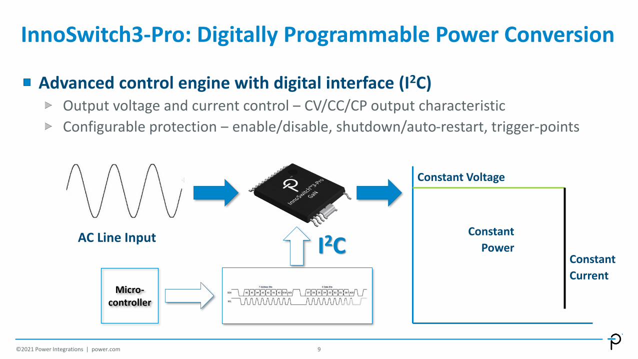
InnoSwitch3-Pro: Digitally Programmable Power Conversion
9©2021 Power Integrations | power.com
I2CAC Line Input
Micro-controller
Constant
Current
Constant Voltage
Constant
Power
Advanced control engine with digital interface (I2C) Output voltage and current control ‒ CV/CC/CP output characteristic
Configurable protection ‒ enable/disable, shutdown/auto-restart, trigger-points

Digital control uses I2C
interface
Programming Interface
10
Load discharge path
• VB/D pin can sink current
Direct load protection• Integrated control of series
N Channel MOSFET Switch
3.6 V supply for
external μC
Communicate via USB
cable to load device• PC / tablet / phone
Programmability• Output voltage and current
• CV, CC and CP profile
• Fault trigger points and response
Adjust output to meet load
requirement• Rapid charge/USB PD
• Adjust/set voltage
• Adjust/set current
• Set protection features
©2021 Power Integrations | power.com

High Integration Enables Cube Designs with Just Two PCBs
12
Power Output 20 W 1C 30 W 1C 65 W 1C
Output 5 V 3 A, 9 V 2.22 A5 V / 3 A, 9 V / 3 A
15 V / 2 A, 20 V / 1.5 APPS: 3.3 – 11 V / 3 A
5 V / 3 A, 9 V / 3 A15 V / 3 A, 20 V / 3.25 A
PPS: 3.3 – 21 V / 3 A
PI Part Number(InnoSwitch3-Pro, PowiGaN)
INN3378C INN3378C INN3370C
Component count 54 54 60
PCB Size (mm) 23.7 x 23 x 24.5 25 x 26 x 27.5 30 x 30 x 34
©2021 Power Integrations | power.com

InnoSwitch4-CZ + ClampZero
©2021 Power Integrations | power.com

Flyback power supplies must use a protection circuit to
prevent the voltage on the primary switch rising too high
after it turns off
Circuit “clamps” voltage and keeps it to safe levelSimplest type is RCD (Resistor, Capacitor, Diode)Energy is diverted to the capacitor (C)
BUT energy in an RCD clamp is lostResistor (R) dissipates the energy (and gets hot)Reduces circuit efficiency
Clamp Circuit in a Flyback
14©2021 Power Integrations | www.power.com COMPANY CONFIDENTIAL
Voltage on Primary Switch of a
Conventional Flyback
Significant overshoot if no
clamp circuit
RCD clamp
VDS
VDS
R C
D

RCD Clamp Compared to Active Clamp
Significant power loss in RCD clampIncreases with switching frequency
Leakage energy heats clamp resistor and diode
Reduces flyback efficiency
Leakage energy recycled through clamp FET
ZVS on flyback switch reduces switching losses
Increases circuit efficiency and reduces
temperature
15©2021 Power Integrations | www.power.com
RCD Clamp Active Clamp
R C
D
Flyback SwitchFlyback Switch
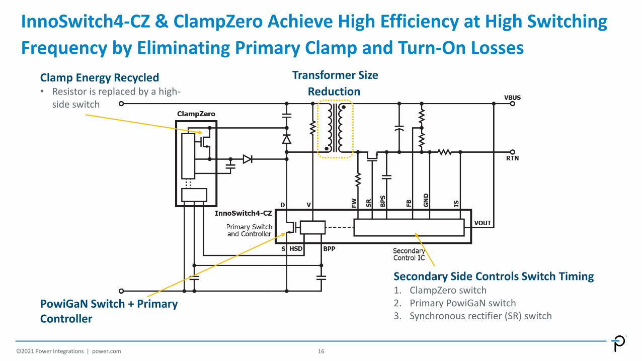
InnoSwitch4-CZ & ClampZero Achieve High Efficiency at High Switching
Frequency by Eliminating Primary Clamp and Turn-On Losses
16
Transformer Size
Reduction Clamp Energy Recycled• Resistor is replaced by a high-
side switch
PowiGaN Switch + Primary Controller
©2021 Power Integrations | power.com
Secondary Side Controls Switch Timing1. ClampZero switch2. Primary PowiGaN switch3. Synchronous rectifier (SR) switch

InnoSwitch4-CZ & ClampZero Family Power Table
17
InnoSwitch4-CZPart Number
ClampZero Part Number
85-264 VAC 385 VDC (PFC Input)
Adapter Open Frame Adapter Open Frame
INN4073C CPZ1061M 65 W 70 W 75 W 80 W
INN4074CCPZ1062M
75 W 85 W 95 W 100 W
INN4075C 80 W 90 W 105 W 110 W
©2021 Power Integrations | power.com
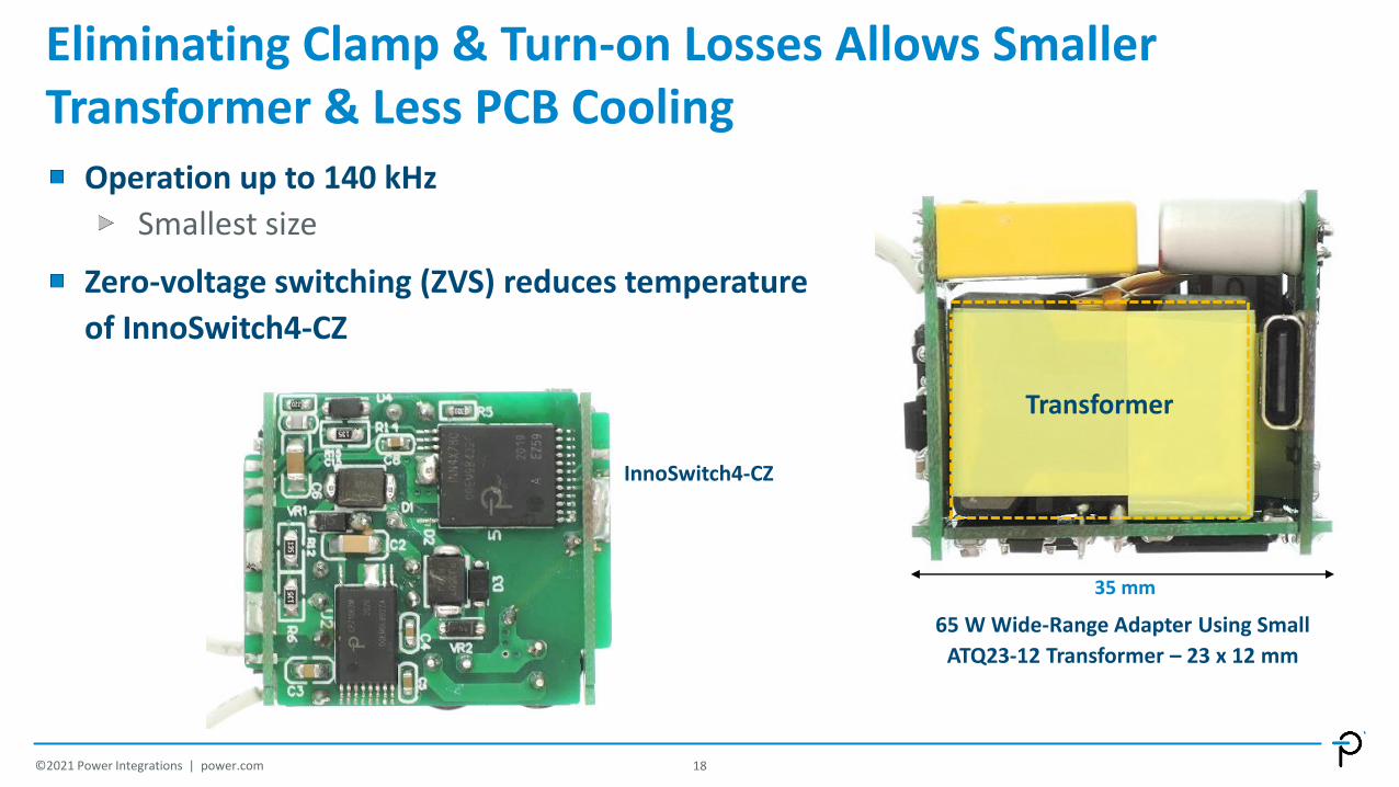
Eliminating Clamp & Turn-on Losses Allows Smaller Transformer & Less PCB Cooling
18©2021 Power Integrations | power.com
Operation up to 140 kHz
Smallest size
Zero-voltage switching (ZVS) reduces temperature
of InnoSwitch4-CZ
35 mm
65 W Wide-Range Adapter Using Small
ATQ23-12 Transformer – 23 x 12 mm
InnoSwitch4-CZ
Transformer

MinE-CAP
©2021 Power Integrations | power.com

Higher Frequency: Limited Size Savings, Added Cost
20©2021 Power Integrations | www.power.com
More EMI = larger input filter
Must add active-clamp circuit to
reduce snubber and switching losses
• Controls peak power
• Is a big device
Smaller Transformer
What about the bulk capacitor?

To Support Higher Voltage, Capacitor Makers Must Increase the Size of the Capacitor – A LOT!
21©2021 Power Integrations | www.power.com
160 V max. voltage
Capacitance: 100 μFCapacitance: 100 μF
400 V max. voltage
18 x 36 mm 13 x 25 mm
~1/3 of volume
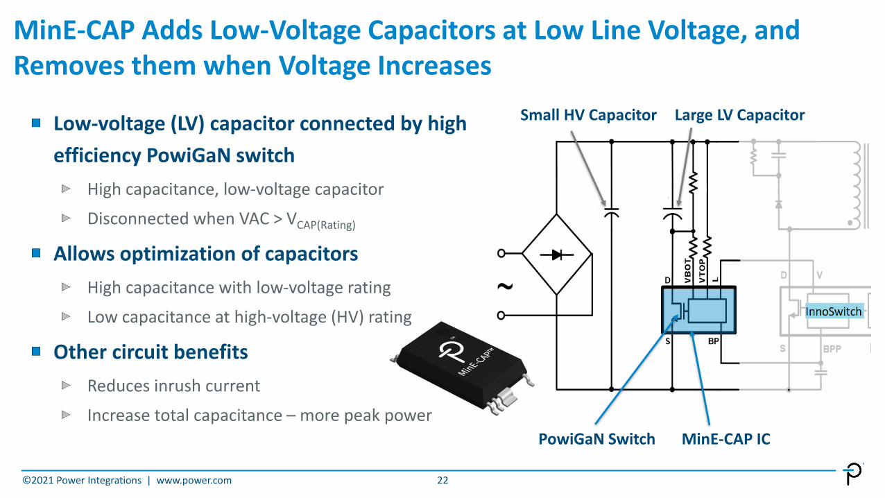
MinE-CAP Adds Low-Voltage Capacitors at Low Line Voltage, and Removes them when Voltage Increases
22©2021 Power Integrations | www.power.com
PowiGaN Switch
Small HV Capacitor Large LV Capacitor
MinE-CAP IC
Low-voltage (LV) capacitor connected by high
efficiency PowiGaN switch
High capacitance, low-voltage capacitor
Disconnected when VAC > VCAP(Rating)
Allows optimization of capacitors
High capacitance with low-voltage rating
Low capacitance at high-voltage (HV) rating
Other circuit benefits
Reduces inrush current
Increase total capacitance – more peak power

InnoSwitch3-PD
©2021 Power Integrations | power.com
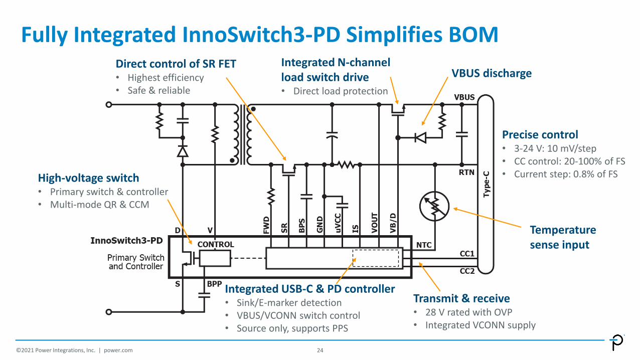
Fully Integrated InnoSwitch3-PD Simplifies BOM
24©2021 Power Integrations, Inc. | power.com
High-voltage switch• Primary switch & controller• Multi-mode QR & CCM
Direct control of SR FET• Highest efficiency• Safe & reliable
Integrated N-channel load switch drive• Direct load protection
VBUS discharge
Precise control• 3-24 V: 10 mV/step• CC control: 20-100% of FS• Current step: 0.8% of FS
Temperaturesense input
Integrated USB-C & PD controller• Sink/E-marker detection• VBUS/VCONN switch control• Source only, supports PPS
Transmit & receive• 28 V rated with OVP• Integrated VCONN supply

InnoSwitch3-PD – Key Features for Rapid Charging
USB Power Delivery controller Supports USB PD 3.0 + PPS & QC4 protocols
One-Time Programmable (OTP) memory
Integration of type-C controller simplifies designCompliant with USB Type-C Rev. 1.3
• Pull-up current-source for “sink” and cable detection
• VCONN supply for electronically marked cables
Overvoltage protection for CC1/CC2 (28 V)
Provides all required USB-PD and PPS functionalityRemoves time/cost of software and interface development
Dedicated temperature sense pin for NTC resistor
25©2021 Power Integrations, Inc. | power.com
InnoSwitch3-PD enables the
highest power density
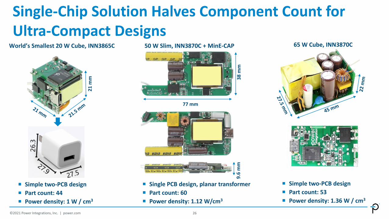
Single-Chip Solution Halves Component Count for Ultra-Compact Designs
©2021 Power Integrations, Inc. | power.com
World’s Smallest 20 W Cube, INN3865C
21
mm
Simple two-PCB design
Part count: 44
Power density: 1 W / cm3
65 W Cube, INN3870C
Simple two-PCB design
Part count: 53
Power density: 1.36 W / cm3
50 W Slim, INN3870C + MinE-CAP
9.6
mm
77 mm
38
mm
Single PCB design, planar transformer
Part count: 60
Power density: 1.12 W/cm3
26
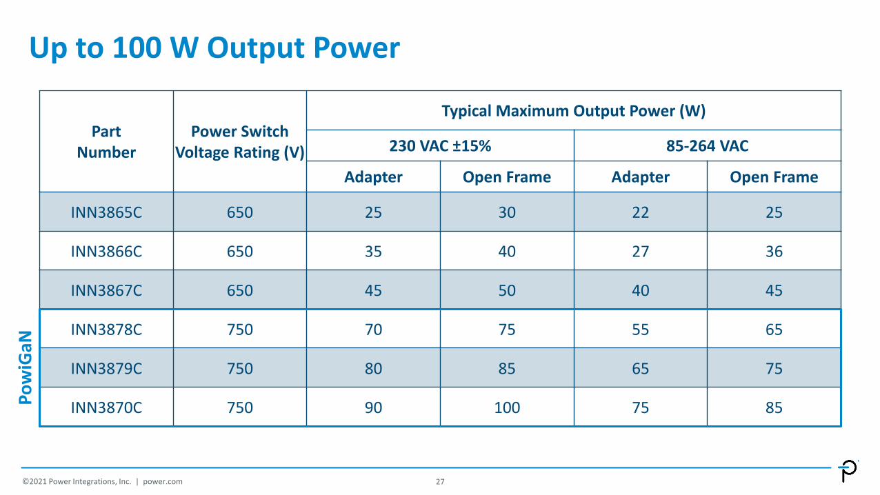
Up to 100 W Output Power
©2021 Power Integrations, Inc. | power.com
PartNumber
Power Switch Voltage Rating (V)
Typical Maximum Output Power (W)
230 VAC ±15% 85-264 VAC
Adapter Open Frame Adapter Open Frame
INN3865C 650 25 30 22 25
INN3866C 650 35 40 27 36
INN3867C 650 45 50 40 45
INN3878C 750 70 75 55 65
INN3879C 750 80 85 65 75
INN3870C 750 90 100 75 85Po
wiG
aN
27

Multi-Port Adapters
©2021 Power Integrations | power.com

InnoSwitch3-Pro Enables Unique Current Sharing Architecture for Multi-Port Chargers
29
Single-stage conversion – 4% more efficient
than conventional topologies
>92% end-to-end efficiency
Lowest component count
Best thermal performance
No hotspots
Eliminates high frequency DC-DC converters
Reduces radiated EMI
©2021 Power Integrations | power.com
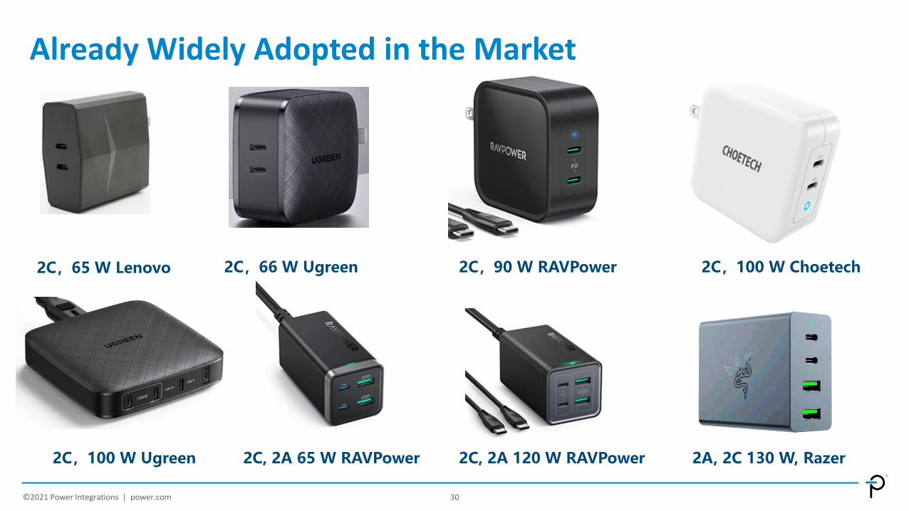
Already Widely Adopted in the Market
30©2021 Power Integrations | power.com
2C,65 W Lenovo 2C,90 W RAVPower
2C,100 W Ugreen
2C,100 W Choetech
2C, 2A 65 W RAVPower 2C, 2A 120 W RAVPower 2A, 2C 130 W, Razer
2C,66 W Ugreen
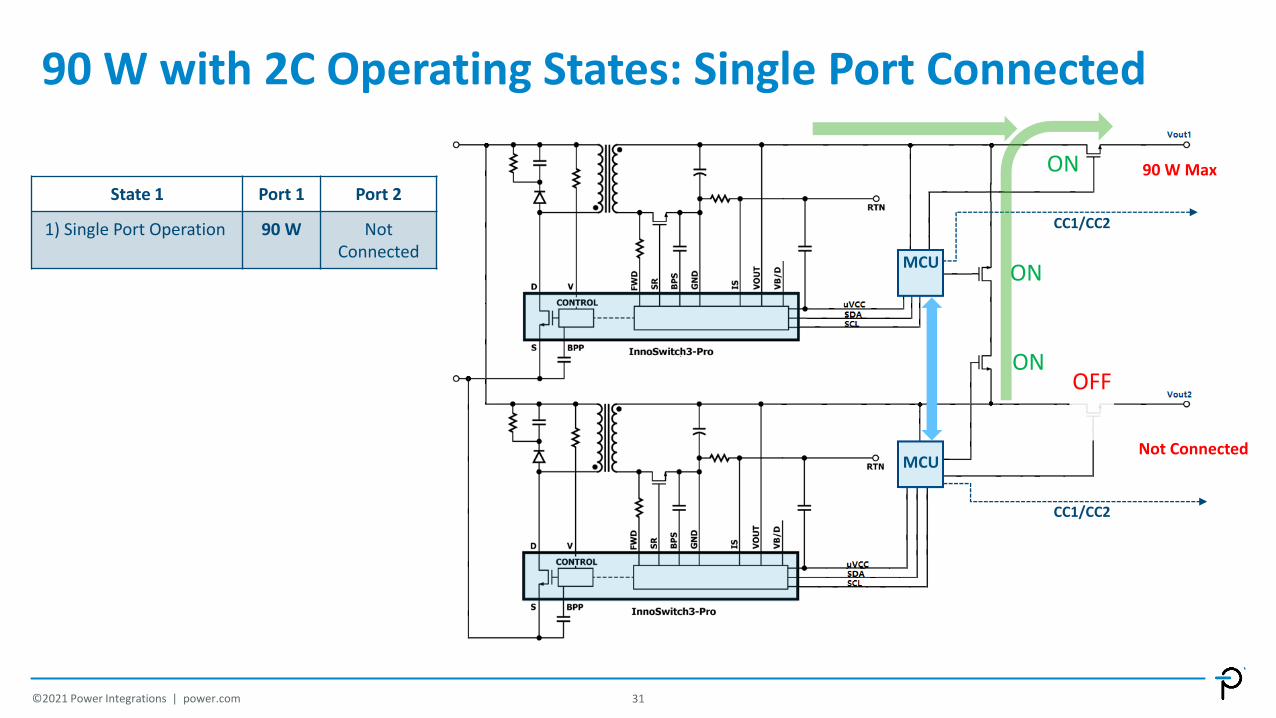
90 W with 2C Operating States: Single Port Connected
31
State 1 Port 1 Port 2
1) Single Port Operation 90 W Not Connected
MCU
MCU
ON 90 W Max
Not Connected
OFF
CC1/CC2
CC1/CC2
ON
ON
©2021 Power Integrations | power.com
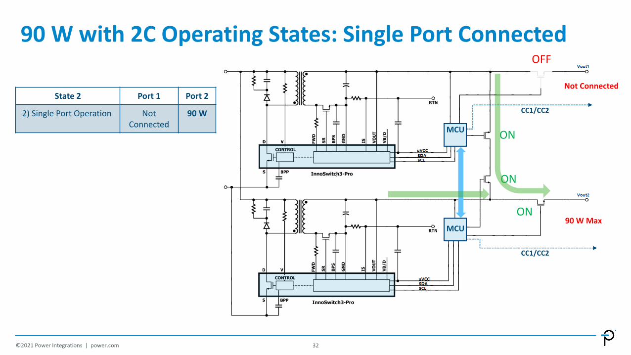
90 W with 2C Operating States: Single Port Connected
32
MCU
MCU
ON90 W Max
Not Connected
OFF
CC1/CC2
CC1/CC2
ON
ON
©2021 Power Integrations | power.com
State 2 Port 1 Port 2
2) Single Port Operation NotConnected
90 W
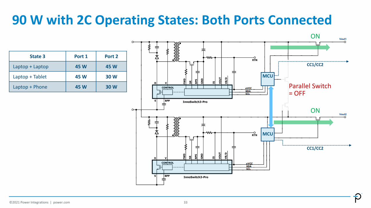
90 W with 2C Operating States: Both Ports Connected
33
State 3 Port 1 Port 2
Laptop + Laptop 45 W 45 W
Laptop + Tablet 45 W 30 W
Laptop + Phone 45 W 30 W
MCU
MCU
Parallel Switch = OFF
ON
CC1/CC2
CC1/CC2
ON
©2021 Power Integrations | power.com
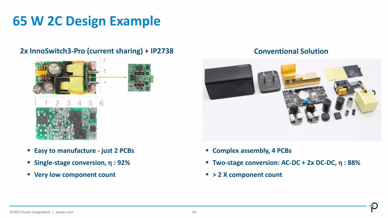
65 W 2C Design Example
34
Easy to manufacture - just 2 PCBs
Single-stage conversion, η : 92%
Very low component count
Complex assembly, 4 PCBs
Two-stage conversion: AC-DC + 2x DC-DC, η : 88%
> 2 X component count
2x InnoSwitch3-Pro (current sharing) + IP2738 Conventional Solution
©2021 Power Integrations | power.com

Next Generation Current Sharing Further Simplifies Design, Reduces System Cost
35©2021 Power Integrations | power.com
Ports in use USB-C1 USB-C2
C1 65 W -
C2 - 65 W
C1 + C2 45 W 20 W
Ports in use USB-C1 USB-A1
C1 65 W -
A1 - 20 W
C1 + A1 45 W 20 W
Ports in use USB-C1 USB-C2 USB-A1
C1 65 W - -
C2 - 65 W -
A1 - - 20 W
C1 + C2 45 W 20 W -
C1 + A1 45 W - 20 W
C2 + A1 - 5 V / 5 A
C1 + C2 + A1 45 W 5 V / 4 A
2C
65 W
1C_1A
2C_1A
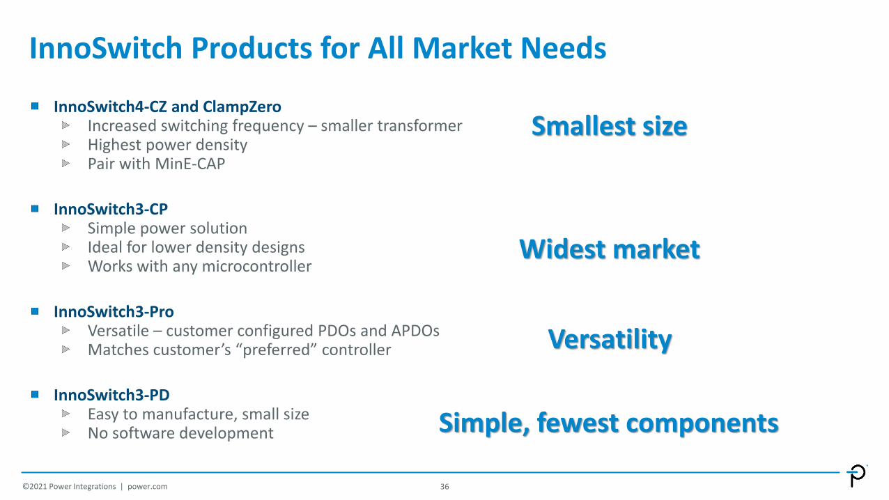
InnoSwitch Products for All Market Needs
36
InnoSwitch4-CZ and ClampZeroIncreased switching frequency – smaller transformerHighest power densityPair with MinE-CAP
InnoSwitch3-CPSimple power solutionIdeal for lower density designsWorks with any microcontroller
InnoSwitch3-ProVersatile – customer configured PDOs and APDOsMatches customer’s “preferred” controller
InnoSwitch3-PDEasy to manufacture, small sizeNo software development
Smallest size
Widest market
Versatility
©2021 Power Integrations | power.com
Simple, fewest components
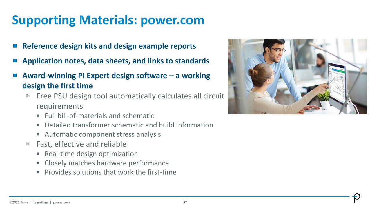
Supporting Materials: power.com
37
Reference design kits and design example reports
Application notes, data sheets, and links to standards
Award-winning PI Expert design software – a working design the first time
Free PSU design tool automatically calculates all circuit requirements• Full bill-of-materials and schematic• Detailed transformer schematic and build information• Automatic component stress analysis
Fast, effective and reliable• Real-time design optimization• Closely matches hardware performance• Provides solutions that work the first-time
©2021 Power Integrations | power.com