Embed Size (px)
Citation preview

NAVAL POSTGRADUATE SCHOOLMonterey, California
AD-A277 84311111111111 lmID il li glmSl
DTIELECTE
THESIS APROQ6, W4)
A GALLIUM ARSENIDE MESFET OPERATIONALAMPLIFIER FOR USE IN COMPOSITE
OPERATIONAL AMPLIFIERS
by
Benjamin L. Hudson
December, 1993
Thesis Co-Advisor: Sherif MichaelThesis Co-Advisor: Douglas Fouts
Approved for public release; distribution is unlimited.
94-10359 MTC QUALiY i:c...'"" 3
94 4 5 051

UNCLASSIFIEDSE"URITY C.ASIP1FCATIKM OF THIS PAGE
REPORT DOCUMENTATION PAGEia REPORT SECURITY CLASSIFICATION UN(LASsIEDa lb. RESTRKT1IVE MWAH3S
2a SECURITY CLASSIFICATION AUTHORITY 3. DISThIBUTION/AVAILABILITY OF REPORTApproved for public mleas; distribution is unlimied.9b). OECLASSIFICATKONVOOWNGRADING SCHEDULE
4. PERFORMING ORGANIZATION REPORT NUMBER(S) 5. RING ORGANIZATION REPORT NUMBER(S)
.NNAMERM/OG ZATION Ob. OFFICE SYMBOL 7. NAME OF MONITORING ORGANIZATION~iW n L~ Parte TIN r appicah(ble) Naval Piostgraduate SchoolNaval Postgraduate School EC
Sc. ADDRESS (City, State, and ZIP Code) 7b. ADDRESS (City, State, and ZIP Code)
Monterey. CA 93943-5000 Monterey. CA 93943-5000
a. NAME OF FUNDINGISPONSORING ab. OFFICE SYMBOL 9. PROCUREMENT INSTRUMENT IDENTIFICATION NUMBERORGANIZATION (If applicable)
Sc. ADDRESS (City, State, and ZIP Code) 10. SOURCE OF FUNDING NUMBERSPROGRAM PROJECT TASK WORK UNITELEMENT NO. NO. NO. ACCESSION NO.
11. TITLE (IncAude Security Classifction)
A GALLIUM ARSENIDE MESFET OPERATIONAL AMPLIFIER FOR USE IN COMPOSITE OPERATIONAL AMPLIFIERS
12. PERSONAL AUTHOR(S) Hudson, Benjamin L.
M-TY F.gOF UEPORT 13b.TIME95CVERED 12N3 , 1I FR•RT (Year, Month, Day) 15. PAGE COUNTwrs =hs (Year Month LINT
16. SUPPLEMENTARY NOTATION
The views expressed in this thesis are those of the author and do not reflect the official policy or positionof the Department of Defense or the United States Government
17. COSATI CODES 18. SUBJECT TERMS (Contnue on reverse if necessary and identity by block number)FIELD__GROUP_ SUB-GROUPI Gallium Arsenide (GaAs). Composite operational amplifier (CNOA),FIELD GROUP SUB-GROUP Schouky-ba'ier Diode (SBD) and Level shifter (LS)
19. AmSTR.ACT (Continuq 9n =usff i En " Adentity by bo nwnbAgallumarsemoe t(a.") MEtFET operational ampluier for use in composite operational amplifier (CNOA)
configurations is described. This device is guaranteed to be suitable for construction in CNOA models. The GaAsop amp design is a general-purpose device that exhibits a low-frequency gain of approximately 32dB and an open-loop unity gain frequency of 1.3GHz. The input offset voltage of the op amp is 2OmV. These parameters are essentialfor optimum composite operational amplifier performance. Development and simulation of the GaAs op amp ispresented.
]]TIC QUALITY IM3ý27CTED 3
20. D •TRIBUTIONAVAILABILITY OF ABSTACT 21. ABSTRACT SECURITY CLASSIFICATION[] UNCLASSIFIED/UNLIMITED Q] SAME AS RPT. [] DTIC USERS UNCLASSIIED
fiq Ffa ESPNI8 INDIVIDUAL 2%ITE 4T (Include Area Code) InghE SMO
DO FORM 1473, 84 MAR 83 APR edition may be used until exIhaused SECURITY CLASSIFICATION OF THIS PAGE
AI other ediis ore obsolete UNCLASSIFIEDi

Approved for public release; distribution is unlimited.
Gallium Arsenide MESFET Operational Amplifier to be used
in Composite Operational Amplifier Design
by
Benjamin Lenward HudsonCaptain, United States Army
B.SE.E., Tuskegee University, 1984
Submitted in partial fulfillment of therequirements for the degree of
MASTER OF SCIENCE IN ELECTRICAL ENGINEERINGfrom the
NAVAL POSTGRADUATE SCHOOLDecember, 1993
Author: °f° Benjamin L.enward Hudson
Approved By:Sherif Michael
Thesis Co-Advisor, ECE Dept
Douglas FoutsThesis Co-Advisor, ECE Dept
Michael A. Morgan, Chairn(A,Department of Electrical and Computer Engineering
ii
Abstract
A gallium arsenide (GaAs) MESFET operational amplifier for use in composite
operational amplifier (CNOA) configurations i described. This device is guaranteed to be
suitable for, )nstruction in CNOA models. The GaAs op amp design is a general-purpose
device that exhibits a low-frequency gain of approximately 32dB and an open-loop unity
gain frequency of 1.3GHz. The input offset voltage of the op amp is 20mV. These
parameters are essential for optimum composite operational amplifier performance.
Development and simulation of the GaAs op amp is presented.
Aoessuon Fr
OTIS GRAS&IDTIC TAB 0UOannouced 0astifloatlo-
MtVibutiof
-A val a-b iI- It y aids
jAtil and/orDist ISpecLal
TABLE OF CONTENTS
IN TR O D U CTIO N ...................................................................................................... 1
II. GALLIUM ARSENIDE (GaAs) MES3FET DEVICES ......................................... 3
A . G EN ERAL ................................................................................................ 3
B. PHYSICAL PROPERTIES OF GaAs MESFETs ...................................... 4
1. COMPARISON BETWEEN MOSFET and MESFET DEVICES ...... 4
2. GaAs PHYSICAL DEVICE MODEL ............................................ 5
3. DC DESIGN CONCERNS ............................................................. 6
4. GaAs FET SPEED ANALYSIS ..................................................... 8
5. GaAs MET OPERATION ............................................................. 10
6. DEVICE GAIN AND UNITY BANDWIDTH ........................... 12
C. GaAs DESIGN TECHNIQUES ............................................................... 15
1. Schottky-Barrier Diodes and Level Shifters ................................. 15
2. Current M irrors ............................................................................ 19
3. Small-Signal gnrdv Effect ............................................................. 20
4. Gain Enhancement Techniques .................................................... 22
D. GaAs DEVICE DESIGN PARAMETERS .............................................. 27
Ill. GaAs MESFET OPERATIONAL AMPLIFIER DESIGN ................................ 31
A . G EN ERA L .............................................................................................. 31
B. GaAs DIFFERENTIAL AMPLIFIER INPUT GAIN STAGE ................ 32
C. LOAD STAGE & COMPLETE OP AMP .............................................. 37
D. OP AMP DRAWBACKS ....................................................................... 38
iv
1. Finite D C G ain ................................................................................... 39
2. Common-Mode Rejection Ratio ........................................................ 38
3. Offset Voltage ............................................................................... 38
4. Effect Bandwidth ........................................................ 40
5. Slew -Rate ...................................................................................... 40
6. Input and Output Impedance ........................................................ 40
IV. COMPOSITE OPERATIONAL AMPLIFIERS ................................................. 41
A. GENERAL .............................................................................................. 41
B. THEORY BEHIND CNOAs .................................................................. 41
C. COMPOSITE OPAMP TOPOLOGIES ................................................... 44
1 . C20A-1 .................................................................. 44
2. C 2O A -2 ......................................................................................... 46
3. C 2O A -3 ......................................................................................... 47
4. C2O A -4 ......................................................................................... 8 4
D. DETERMINING APPROPRIATE a and k VALUES ........................... 50
E. GREATER BANDWIDTH USING C2OAs ............................................ 50
F. C2OAs COMPONENT SENSITIVITY ................................................... 50
G. OFFSET VOLTAGES ............................................................................ 51
H. C2OA SLEW-RATE CONSIDERATIONS ............................................ 56
V. SIMULATION RESULTS ................................................................................. 53
A. GENERAL .............................................................................................. 53
B. POWER SUPPLY ................................................................................... 53
C. ESTABLISHED FINITE GAIN .............................................................. 53
D. OPEN-LOOP ANALYSIS ....................................................................... 53
v

E. CLOSED-LOOP ANALYSIS ....................................................................... 59
VI. CONCLUSIONS AND RECOMMENDATONS .................................................... 58
A . CO N CLU SIO N S ........................................................................................... 58
B. RECOMMENDATIONS FOR FUTURE RESEARCH .......................... 58
LIST OF REFERENCES .............................................................................................. 59
INITIAL DISTRIBUTION LIST ................................................................................. 63
vi

LIST OF TABLES
Table 2.1 VITESSE GaAs SCHOTFKY DIODE PARAMETER VALUES ........ 17
Table 2.2 GATE CAPACITANCE & DC MODEL PARAMETERS ................. 28
Table 2.3 TEMPERATURE EFFECT PARAMETERS ...................................... 29
Table 3.1 OP AMP PERFORMANCE PARAMETER VALUES ....................... 33
Table 3.2 DIFFAMP ELEMENT DIMENSIONS ................................................ 37
Table 4.1 INPUT OFFSET VOLTAGE ................................................................ 52
Table 5.1 OP AMP PERFORMANCE PARAMETERS ....................................... 57
vii
LIST OF FIGURES
Figure 2.1 n-Channel Cross-Sectional areas of MOS and MES Devices ................ 4
Figure 2.2 Cross-Section of a GaAs Schottky-Barrier Diode & MESFET .............. 5
Figure 2.3 Device Characteristics of an Inverter NMOS & MESFET Circuit ..... 6
Figure 2.4 MESFET Drain Current vs. Drain-to-Source Voltage ........................... 7
Figure 2.5 n-Channel Depletion Type GaAs MESFET Symbol ............................. 8
Figure 2.6 Single-Stage Active Load GaAs Amplifier ........................................... 9
Figure 2.7 Cross-Sectional of Schottky-Barrier Diode ............................................... 11
Figure 2.8 Sample SBD Level-Shifter .................................................................. 13
Figure 2.9 GaAs MESFET Current Mirror ........................................................... 16
Figure 2.10 Small-Signal Equivalent GaAs MESFET Model ................................ 19
Figure 2.11 MESFET Output Resistance vs. Frequency ........................ 20
Figure 2.12 Depletion-mode GaAs Differential Amplifier ...................................... 21
Figure 2.13 MESFET Current Source ..................................................................... 22
Figure 2.14 GaAs Cascde Current Source ............................................................. 23
Figure 2.15 GaAs MESFET Bootstrapping Current source ..................................... 25
Figure 2.16 GaAs Cascode Current Source ............................................................. 26
Figure 2.17 Basic Circuit Configuration for GaAs Bootstrapping ........................... 27
Figure 3.1 D-MESFET Operational Amplifier ..................................................... 32
Figure 3.2 Single-Ended Equivalent Circuit Model ........................... 35
Figure 3.3 GaAs Difamp Input Stage ..................................................................... 36
Figure 3.4 General-Purpose GaAs D-MESFET Opamp ....................................... 38
viii
Figure 4.1 N ullator, N orator, and N ullor .................................................................... 43
Figure 4.2 Basic Composite Opamp Symbol ........................................................ 44
Figure 4.3 C2O A -I ................................................................................................ 45
Figure 4.4 C2O A -2 ................................................................................................ 47
Figure 4.5 C2O A -3 ................................................................................................ 48
Figure 4.6 C2O A -4 ................................................................................................ 49
ix
L INTRODUCTION
The Operational Amplifier (op amp) is arguably the most powerful analog integrated
circuit (IC) in the electronics industry. Its multiuse is unprecedented. Op asnp applications
can range from simple designs like those found in RC timers to more complex circuitry
involved in high-speed switching, computer signal processing, and radars. Over the years,
op amps have evolved and matured form the early days of huge vacuum tubes the size of
breadboxes to microcomponents that can rest on the tip of a finger. Yet, these devices are
not flawless. Its high unit gain frequency (f), at the cost of increased distortion, limited
bandwidth, and low slew-rate are a few of the drawbacks resident to the op amp. This
research will attempt to develop a general-purpose GaAs op amp that could adequately be
used in composite operational amplifiers (CNOAs), with subsequent use in switched-
capacitor filter networks.
Even though the application of GaAs technology in analog VLSI design is somewhat
recent, it has been employed in digital and microwave systems since shortly after its
discovery. GaAs MESFET technology first stepped onto the scene in the early 1970's.
Early test data results were laboratory based only. Yet, its performance was very promising.
The GaAs MESFET offers superior bandwidth and a high ft as compared to its silicon
competitor. It is for this characteristic that a GaAs MESFET device was chosen for
development with future use in composite op amps.
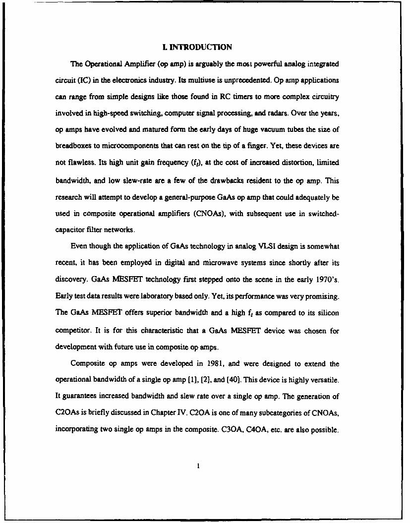
Composite op amps were developed in 1981, and were designed to extend the
operational bandwidth of a single op amp [1], [2], and [40]. This device is highly versatile.
It guarantees increased bandwidth and slew rate over a single op amp. The generation of
C2OAs is briefly discussed in Chapter IV. C2OA is one of many subcategories of CNOAs,
incorporating two single op amps in the composite. C3OA, C4OA, etc. are also possible.
I

Limitations customarily associated with single op amp designs are significantly mitigated
in C2OA configurations. Although, C2OAs will not be designed and simulated in this
research, a background discussion is necessary to provide a framework in which to develop
the GaAs op amp.
By incorporating GaAs technology, C2OA designs will lead to an op amp that
possesses a substantial increase in bandwidth. They will have immediate application in
switched-capacitor filters, analog converters, signal processing, and several other designs.
The following Chapters will provide greater insight concerning the topics just
mentioned. GaAs MESFET physical properties, operation, and equivalent circuit models
are presented in Chapter IH. The actual GaAs op amp design is in Chapter In. Chapter IV
discusses the various composite op amp topologies. Chapter V provides simulation results
of the GaAs op amp. The final Chapter contains the study conclusions and
recommendations for future research.
S. . . . • ! mm i l • om m n • • . . . .. . . . .... . .. ..

H. GALLIUM ARSENIDE (GaAs) MESFET DEVICES
A. General:
Gallium arsenide integrated circuit technology has evolved into an extremely viable
choice for achieving high-speed and wide bandwidth in digital and analog circuits
respectively. This compound semiconductor is formed from gallium and arsenic. It is duly
noted for its high drift mobility (gn) and peak electron velocity as compared to silicon. This
results in higher f, in GaAs transistors than in comparable Si transistors [3] and [6].
While GaAs integrated circuit technology is somewhat new in analog VLSI
applications, it has been used for a number of years in microwave and digital integrated
circuits. As the cost of GaAs decreases its role in analog ICs will increase. Advances in
GaAs ICs will provide inroads for improved switched-capacitor filters, A/D and D/A
converters, and large-signal multipliers. Other applications that have benefitted from this
technology include video processing, radar systems, ground based navigation systems,
FDM telephone, data communications, etc.
This Chapter will focus on the physical properties of GaAs MESFET devices and
some of the key parameters involved in the design of ICs. A brief discussion on level
shifters using schottky-barrier diodes, differential amplifiers (diffamp), bootstrapping,
current mirrors, and other circuit configurations will be presented. Also, some MOS
equivalent circuit models and analog components will be presented. These techniques are
vital in the development of GaAs operational amplifiers. In no way will this section attempt
to cover all the known methods used in building GaAs MESFET ICs. Last, a discussion
about the simulation software tool and its specific parameter values used in the research
will be given.

B. Physical Properties of GaAs MESFETs:
1. Comparison Between MOSFET and MESFET Devices:
GaAs MESFETs offer improved high frequency performance over silicon
MOSFETs. The two major differences between the devices are: (1) how the channel is
formed and (2) how tat gate-control electrode is coupled to the channel. First, the channel
of the device is formed by GaAs or Si semiconductor material, based on the required
application. Second, in a MOSFET, the gate-control electrode is separated from the channel
by a thin oxide dielectric layer. Conversely, a MESFET uses a thin doped channel the
thickness of which is controlled by the depletion of the metal semiconductor junction.
Basically, the metal gate-control electrode is directly connected to the channel [3]. Figure
2.1 illustrates the two different types of gate structures for MOSFET and MESFET devices
respectively.
(a) (b)
+ +
D D
(c) (d)
Fig. 2.1 n-channel cross-sectional areas of (a) MOSFET (b) MESFETand device symbols (c) MOSFET (d) MESFET
4
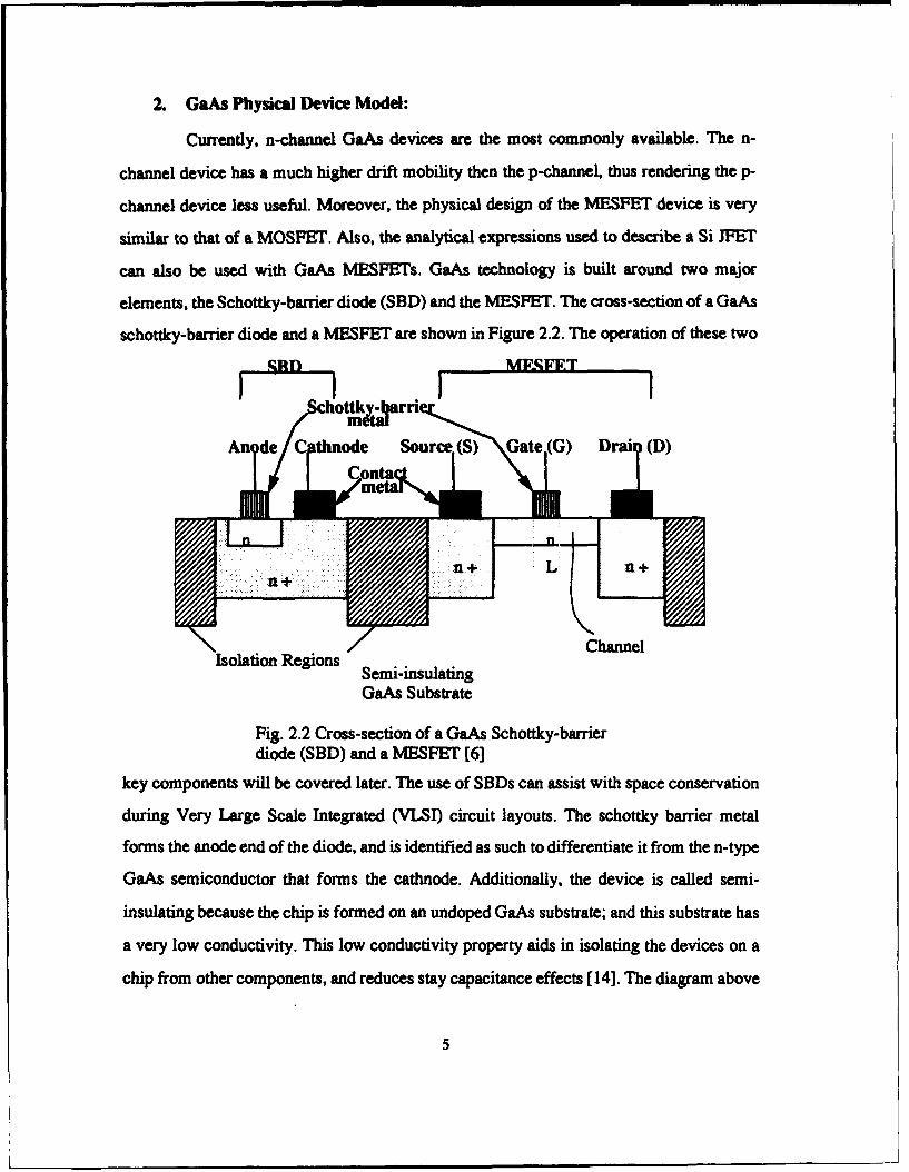
2. GaAs Physical Device Model:
Currently, n-channel GaAs devices are the most commonly available. The n-
channel device has a much higher drift mobility then the p-channel, thus rendering the p-
channel device less useful. Moreover, the physical design of the MESFET device is very
similar to that of a MOSFET. Also, the analytical expressions used to describe a Si NET
can also be used with GaAs MESFETs. GaAs technology is built around two major
elements, the Schottky-barrier diode (SBD) and the MESFET. The cross-section of a GaAs
schottky-barrier diode and a MESFET are shown in Figure 2.2. The operation of these two
7SB I] MFF I
An d node Source (S) G ) Drai (D)
Contact
Sn.+ L 11 +
S/ Channel
Isolation Regions Semi-iulatg
GaAs Substrate
Fig. 2.2 Cross-section of a GaAs Schottky-barrierdiode (SBD) and a MESFET [6]
key components will be covered later. The use of SBDs can assist with space conservation
during Very Large Scale Integrated (VLSI) circuit layouts. The schottky barrier metal
forms the anode end of the diode, and is identified as such to differentiate it from the n-type
GaAs semiconductor that forms the cathnode. Additionally, the device is called semi-
insulating because the chip is formed on an undoped GaAs substrate; and this substrate has
a very low conductivity. This low conductivity property aids in isolating the devices on a
chip from other components, and reduces stay capacitance effects [14]. The diagram above
5

provides an excellent cross-sectional view of how the MESFET and SBD elements are
comprised. For a more extensive look at these elements see [3], [6], (14], [15], [16], and
(17].
3. DC Design Concerns:
The major advantage a GaAs MESFET has over silicon is its much higher gain-
bandwidth product (GBWP). However, a setback to the device is its dc characteristics as
compared to silicon, such as gain. Low gain in GaAs MESFET causes low DC gain in GaAs
op amps. Another problem often encountered in GaAs IC design is low frequency
oscillation (30]. It is believed that a voltage applied across the semi-insulating GaAs
material could cause a negative resistance which is responsible for the low frequency
oscillations. Specific dc characteristic concerns germane to the operational amplifier used
in this research are presented in sub-paragraph (d) of this Chapter.
The most fundamental difference between the MOSFET and ME.SFET device is
the forward dc conduction limit of the MESFET at the gate-to-channel junction. Because
of this dc conduction, the MESFET circuit is less robust in a noisy environment. Figure 2.3
depicts a MOSFET (NMOS) simple inverter device characteristics with a load resistor RL
ID Device Slope=i/rON
Di.ode Slope=l/rD
7tloSe=-N/RL
0 VOMIN VOMAX Vv VDSFig. 2.3 Device characteristics of a simple inverterNMOS and MESFET equivalent circuit.
and a diode for a MESFET p-channel equivalent circuit model. Using the basic NMOS
circuit model already developed makes it easier to design new circuit models for GaAS
6
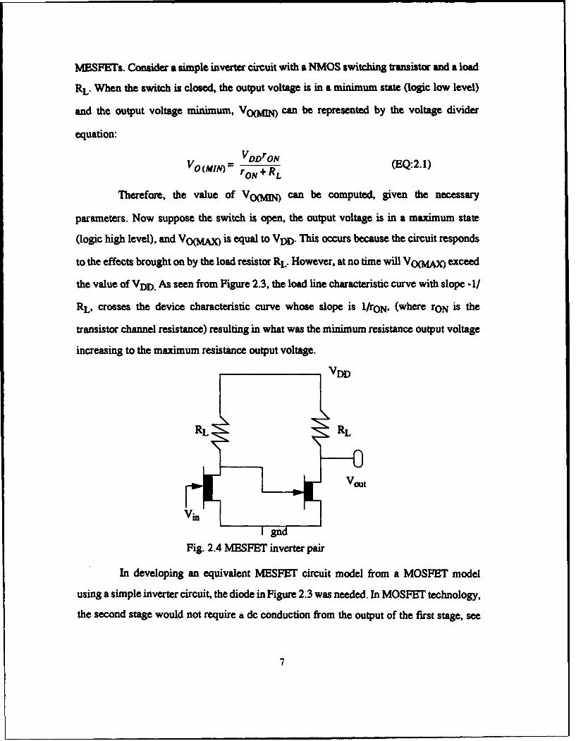
MESFErs. Consider a simple inverter circuit with a NMOS switching transistor and a load
RL. When the switch is closed, the output voltage is in a minimum state (logic low level)
and the output voltage minimum, VOMM can be represented by the voltage divider
equation:
VDDrON (EQ:2.1)VO(MIN)- rON+ RL
Therefore, the value of VO(N can be computed, given the necessary
parameters. Now suppose the switch is open, the output voltage is in a maximum state
(logic high level), and VO(MAX) is equal to VDD. This occurs because the circuit responds
to the effects brought on by the load resistor RL. However, at no time will Vq(MAX) exceed
the value of VDD" As seen from Figure 2.3, the load line characteristic curve with slope -I/
RL, crosses the device characteristic curve whose slope is I/rON, (where rON is the
transistor channel resistance) resulting in what was the minimum resistance output voltage
increasing to the maximum resistance output voltage.
VDD
RL RLRL• "•RL
I gnd
Fig. 2.4 MESFET inverter pair
In developing an equivalent MESFET circuit model from a MOSFET model
using a simple inverter circuit, the diode in Figure 2.3 was needed. In MOSFET technology,
the second stage would not require a dc conduction from the output of the first stage, see
7
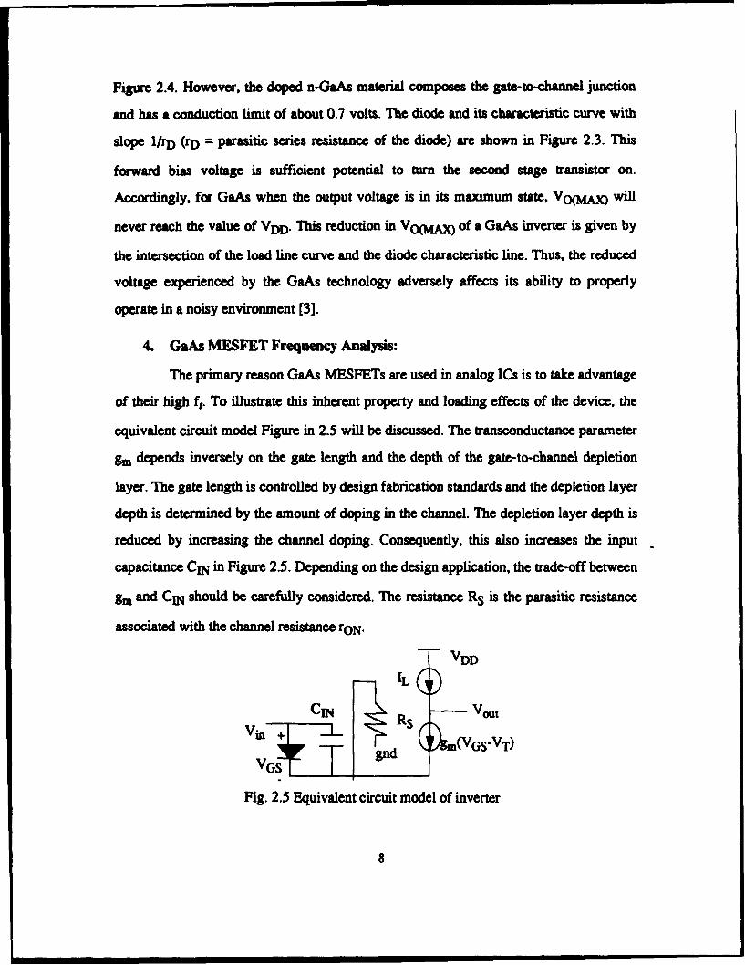
Figure 2.4. However, the doped n-GaAs material composes the gate-to-channel junction
and has a conduction limit of about 0.7 volts. The diode and its characteristic curve with
slope I/rD (rD = parasitic series resistance of the diode) are shown in Figure 2.3. This
forward bias voltage is sufficient potential to turn the second stage transistor on.
Accordingly, for GaAs when the output voltage is in its maximum state, VO(MAX) will
never reach the value of VDD. This reduction in VO(MAX) of a GaAs inverter is given by
the intersection of the load line curve and the diode characteristic line. Thus, the reduced
voltage experienced by the GaAs technology adversely affects its ability to properly
operate in a noisy environment [3].
4. GaAs MESFET Frequency Analysis:
The primary reason GaAs MESFETs are used in analog ICs is to take advantage
of their high ft. To illustrate this inherent property and loading effects of the device, the
equivalent circuit model Figure in 2.5 will be discussed. The transconductance parameter
gm depends inversely on the gate length and the depth of the gate-to-channel depletion
layer. The gate length is controlled by design fabrication standards and the depletion layer
depth is determined by the amount of doping in the channel. The depletion layer depth is
reduced by increasing the channel doping. Consequently, this also increases the input
capacitance CIN in Figure 2.5. Depending on the design application, the trade-off between
gm and CIN should be carefully considered. The resistance RS is the parasitic resistance
associated with the channel resistance rON.
VDD
CIN R - Vout
VGS jj j gnd m(VGsVT)
Fig. 2.5 Equivalent circuit model of inverter
8

The behavior of the MESFET dependent drain current ID is a key performance
parameter of FET IC design. Its characteristics can best be shown by using the curves inFigure 2.6. It is clear from the curves below that the drain current, with respect to the drain-
ID VGS1
VGS2
VGS3VD~sat VGS VT
VD, sadsVDS
D tl YVD . VDs
Fig. 2.6 MESFET drain current vs. drain-to-source voltage
to-source voltage, is nonlinear. The family of MESFET curves is generated by equally
incrementing VGS' beginning at VT as indicated in the Figure. VD.Sat represents the drain
current saturation point for each curve. The effects of this saturation current is a functionof the velocity of the electrons not increasing proportionally with the electric field in thechannel. This effect also relates to the gate length adjustment shown on Figure 2.2.Therefore, the gate length plays a critical role in the amount of drain current in the device.
Decreasing gate length and increasing the electric field in the channel will result in an
earlier saturation drain current. So, in order to produce a small VDS, a short gate length
should be employed. The transconductance parameter scales inversly in MESFETs for long
gate length (L>5gtm), as previously mentioned. Usually, this capacitance is managedduring the layout phase of the design. Increased capacitance can often be obtained byincreasing layout capacitance between transistor stages. Additionally, a short gate length is
advantageous to increasing device transconductance and reducing input capacitance (CIN).
This will be explained in further detail in the GaAs FET operation paragraph. Lastly, the
9

gate length and width of the device are two critical design parameters in the fabrication of
GaAs integrated circuit technology.
5. GaAs FET Operation:
Now to explore how the device works and some of the analytical equations that
are associated with its operation. The MESFET operates somewhat like the Si JFET device
and many of the expressions used to describe the IET are applicable to the MESFET, so
long as no design properties are ignored. In a MESFET, a depletion region forms under the
gate contact surface and the rate and depth of this depletion area is determined by the gate-
to source voltage VG$. The depletion in the channel changes the dimensions of the channel,
and the current that flows from drain to source for some applied ac voltage vDS. Moreover,
it is through this ac drain-to-source voltage that abating occurs at the drain end, which
ultimately results in pinch-off.
Currently, depletion mode GaAs MBSFETs are the most used devices in industry.
The circuit symbol for an n-channel depletion-type GaAs MESFET is shown at Figure 2.7.
The arrow on the device will always point inward, since p-channel devices aren't used. The
threshold voltage for these devices typically range from -0.4 to -4.0. MESFETs normally
operate with a vGS from negative Vt to a small positive voltage not to exceed the breakdown
schottky-barrier voltage at the gate-to-channel junction, which is roughly 0.7 volts. Once
the gate-to-source voltage approaches the barrier breakdown voltage, gate conduction
occurs. Recall from earlier discussion that gate conduction does not take place in a
MOSFET. Gate conduction in a MESFET is a considerable drawback in the operation of
GaAs devices. Once gate conduction occurs, the gate-to-source voltage no longer controls
the critical drain-to-source current IDS. For this research, depletion type devices were used
to design the GaAs amplifier.
Even though enhancement mode MESFETs are not used in this research, some
are available. The enhancement MESFET has a threshold voltage between 0. 1 and 0.3.
Refer to [8] for a more detailed study on enhancement MESFETs.
10

In [31] it was manifested that equation 2.2 is a valid drain current-to-gate voltage
relationship for long gate length MESFETs without being greatly influenced by the doping
quantity:
'D, Sat= 0 (VGs - VT ) 2 (EQ:2.2)
The parameter P is the transconductance parameter of the FET. An analytical
expression for 0, [32] is given in equation 2.3.
2esI'nVsatW (EQ:2.3)
b (gnVpo +3vsa)
This is an excellent expression to illustrate the relationship of the drain current ID
and other key design parameters of the device. It shows how the drain current depends on
both the drift mobility and saturated drift velocity. Furthermore, the equation indicates that
the width and length can improve the current by selecting the appropriate values for each.
Note, that for long L, equation 2.3 reduces to I/L. Now, for shorter gate length, the current
increases less rapidly than the ratio I/L as the gate length is reduced. Also, adjusting the
width and length of the MESFET is a common practice used by IC designers to improve
device performance. The necessary models and equations needed to execute a program are
often already included in the circuit simulation software tool (HSPICE was used in this
research). More on MESFET width and length adjustment in Chapter III. Vpo is the pinch-
o.f voltage, and the reader should refer to [32] for information on E. and b.
D
G
SFig. 2.7 n-channel depletiontype GaAs MESFET symbol
11

Ignoring the velocity saturation effects of a first order MESFET will allow the use
of ]FET equations with only minor errors. These are basic MET expressions and can be
found in a general textbook on electronic integrated circuits.
The ac small-signal model for a MESFET is the same as for any WFET. Two of the
essential ac parameters are gm and ro. They are determined as shown below:
gtn= 2 0 (VGs - VI) (1 + XVDs) (EQ:2.4)
r ( I (EQ:2.5)
In a MESFET, the valueX ranges from 0.1 to 0.3 V-1 , which results in a small ro
component. The low small-signal model output resistance adversely affects the operation
of the device. This ultimately causes a low voltage gain at each stage. Methods to increase
the ro value are contained in paragraph c. This is a major limiting factor in GaAs op amps,
and limits open-loop gain.
6. Device Gain and Unity Bandwidth:
The greatest advantage a GaAs MESFET has over a silicon MOSFET is its much
higher ft. But, the resulting low open-loop gain in a GaAs op amp is a drawback. An
extremely important ac parameter of the MESFET is transconductance gm. It plays a
significant role in the amount of open-loop ac voltage gain obtainable. Transconductance
is defined as follows:
gm= [ "D ] V,, (EQ:2.6)
(TGS simcnta
It is obvious from the expression above that the transconductance varies as a
differential change in the ratio of ID to VGS for a constant VDS. As such, it is closely related
to the gain of a device. Now to explore the effects of gm in a circuit application. A basic
12

single-stage amplifier will be examined, as pictured in Figure 2.8. Note that the circuit uses
I VDD
E: -vou~t
gnd
Fig 2.8 Single-stage active load GaAs amplifier
an active load in place of a resistor. The active load configuration is commonly used in IC
design. Because it is easier to control the characteristics of a MESFET than the
characteristics of a resistor. The resistor load would occupy more real estate on a chip as
compared to an active load transistor. The load transistor is a depletion-mode MESFET
with VGS=O. Thus, higher gains can be achieved by providing sufficient supply voltage to
maintain the active load device in the saturation region. This technique is employed quite
extensively in MESFET ICs and is presented again in the amplifier design techniques
paragraph. An ac analysis for the voltage gain Av of Figure 2.8 is given as:
AV = VOW = .gMRL (EQ:2.7)g~s
Here, the ac voltage open-loop gain is a function of the transconductance
component of the device and the load resistor. However, a more useful expression for g.
of a MESFET is one that includes the drain current limit caused by velocity saturation. In
[3] such a relationship for g. is given by:
13

=svsatW (EQ:2.8)
gin- d
where d is the doping distribution of N-type material in the channel of the device,
and gm varies inversely with d. Hence, to increase the value of gS, the doping distribution
must be reduced. To accomplish this requires increasing the channel doping. Observe that
g. depends inversely on the gate length L.
The transconductance parameter is vital to increased voltage gain but is not the
only parameter affecting the frequency response. Therefore, the MESFET frequency
response is better described by the unity gain frequency (ft). This is measured by short
circuiting the output of the high-frequency small-signal model of the FET. The unity gain
frequency is expressed as:
gmgm (EQ:2.9)2n (Cs + Cgd)(
From this relationship it shows that the unity gain frequency is directly dependent
on the transconductance. Thereby, increasing gm has a positive effect on the bandwidth of
the FET. Also, small-signal model gate capacitances Cgs and Cgd are a function of the gate-
to-source and the gate-to-drain voltages. These capacitances should be minimized to
improve the frequency response. An expression for ft in terms of the gate length is more
practical and desirable. Equation 2.10 (see [8] for derivation) below is more concise and
useful:
f Vsat
2nL (EQ:2. 10)
This equation is used to estimate the unity frequency in the amplifier design stage
and it compares favorably with already fabricated and tested ICs. Moreover, ft varies
inversely proportional to the gate length L. This will remain true so long as the gate
capacitances maintain a direct relationship with the gate length. This effect can be disrupted
by the fringing capacitance [33] which is caused by horizontally expanding the depletion
14
layer in the direction of the gate metal. Thus, to obtain maximum gain g., through reduction
of gate length, it would require sophisticated fabrication technology and controlling doping
in the channel so that the ratio of fringing capacitance to plate capacitance stays modestly
small. Besides, the added gain would be negligible as compared to the corresponding
increase in bandwidth. Accordingly, a cost-efficiency trade-off analysis may prove
beneficial. The GaAs amplifier analyzed and presented in Chapter MI was simulated with
a minimum gate length of 0.81Lm. This is the smallest length the fabricator could reliably
produce.
C. GaAs Design Techniques:
In this section, a few GaAs circuit design techniques and models associated with the
construction of MESFET amplifier ICs will be presented. Also, a general purpose GaAs
amplifier with reasonable gain (40dB) is offered. In addition, a method frequently used to
overcome the low output resistance ro in FETs when in saturation is given. Techniques
discussed will focus mostly on the specific circuit design of the amplifier used in Chapter
lIf; nevertheless, others will be outlined. This section is not intended to be all inclusive of
the techniques and models that have been developed in recent years. However, other
sources addressing and expanding on this topic are found in [3], [4], [8], and [10].
1. Schottky-Barrier Diodes and Level Shifters:
Both the schottky-barrier diodes (SBD) and voltage level shifter (VLs) are key
elements in GaAs MESFET IC applications. The schottky-barrier diode is a special type of
diode that is formed from carefully doped n-type material. Figure 2.9 provides an excellent
cross-sectional look at the schottky diode composition. As stated in previous sections, the
schottky metal rests on the depletion layer (anode) and the ohmic contact to form the
cathnode.
15

metal ChannelDepletion Ohccnatimplant
layer Ohmeta
Source & drain
Semi-insulating GaAs implant
Fig 2.9 cross-sectional of schottky-barier diode
A current-voltage characteristic curve of the schottky diode appears nearly the
same as the pn-junction diode. The current flow of the schottky diode device is significantly
different from the pn-junction diode in that the majority carriers (electrons) allow the
conduction current and reverse saturation current. As a result, there is no large collection
of minority carriers (holes) in the bulk region at doping amounts above a prescribe level.
Since the diffusion capacitance in schottky diodes is negligible, it results in much faster
transition time from forward bias to reverse bias as compared to the pn-junction diode.
Because of these properties, the SBD is also identified as a majority carrier device. A
properly n-type doped schottky metal has a voltage breakdown between 0.60 and 0.70volts,
depending on the concentration of n-type doping. Therefore, significant forward bias
current flow will occur after voltage breakdown. Continuing, the SBD's current-voltage
characteristic curve is identical to the ideal diode I-V curve, and is given by:
ID)= 1,[expqV 5D, -_] (EQ:2.11)Is~xP(nkT J
Is in this expression is the diode saturation current, n is the ideality factor or the
emission coefficient. The variables q, k and T are charge, Boltzmann's constant, and
16
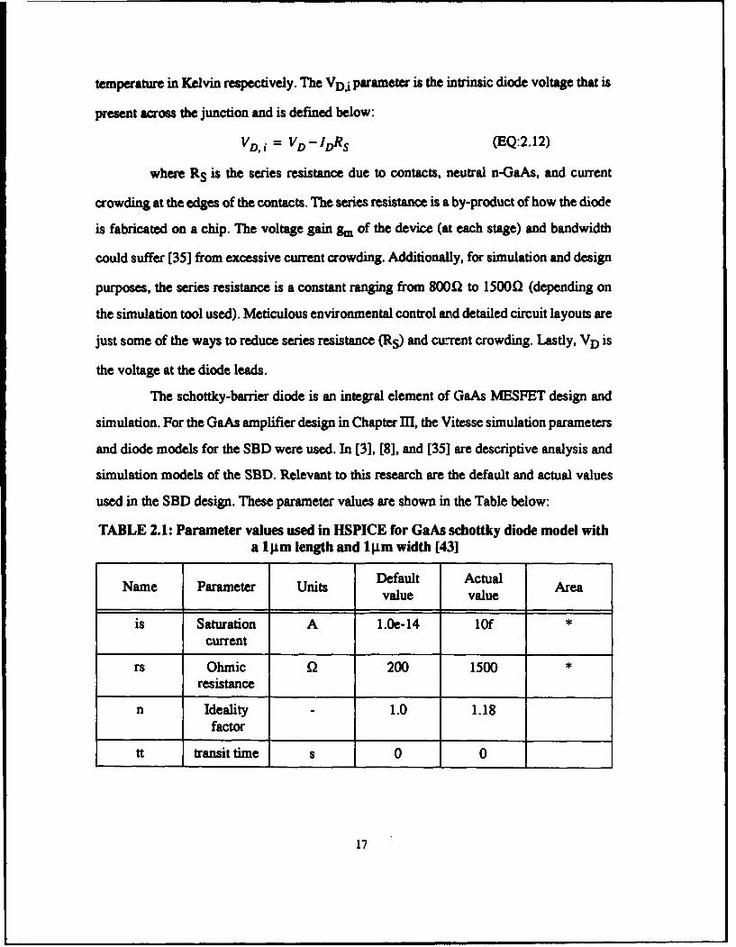
temperature in Kelvin respectively. The VD4 parameter is the intrinsic diode voltage that is
present across the junction and is defined below:
VD, -= VD -IRs (EQ:2.12)
where RS is the series resistance due to contacts, neutral n-GaAs, and current
crowding at the edges of the contacts. The series resistance is a by-product of how the diode
is fabricated on a chip. The voltage gain gm of the device (at each stage) and bandwidth
could suffer [35] from excessive current crowding. Additionally, for simulation and design
purposes, the series resistance is a constant ranging from 8000 to 15000 (depending on
the simulation tool used). Meticulous environmental control and detailed circuit layouts are
just some of the ways to reduce series resistance (RS) and current crowding. Lastly, VD is
the voltage at the diode leads.
The schottky-barrier diode is an integral element of GaAs MESFET design and
simulation. For the GaAs amplifier design in Chapter III, the Vitesse simulation parameters
and diode models for the SBD were used. In [3], [8], and [35] are descriptive analysis and
simulation models of the SBD. Relevant to this research are the default and actual values
used in the SBD design. These parameter values are shown in the Table below:
TABLE 2.1: Parameter values used in HSPICE for GaAs schottky diode model witha lgm length and lnm width [43]
Ums Default ActualName Parameter Units val Areavalue value
is Saturation A 1.0e-14 lOf *
current
rs Ohmic Q 200 1500 *
resistance
n Ideality 1.0 1.18factor
tt transit time s 0 0
17

TABLE 2.1: Parameter values used in HSPICE for GaAs schottky diode model witha 1 im length and Igm width [43]
Name Parameter Units Default ActualAreavalue value
cjo Zero-bias F 0 2.0e-15 *junction
capacitance
vj Built-in V 1 0.8potential
m Grading 0.5 0.5coefficient
rd Drain resis- Q 500 3Ktance
r. Source .0 500 3K
resistance
The asterisk (*) above indicates that the parameter is to be scaled with respect to
the diode area. The scaled factor is usually defined in the model line and is intended to
provide the designer greater flexibility in obtaining optimum circuit performance. For most
software simulation tools the SBD's length (1 gm to 3 gm) is preset and the area of the SBD
is determined by scaling the width parameter. Schottky-barrier diodes are constructed by
connecting together the drain and source terminals of a MESFET transistor.
Some of the Vitesse diode parameter values are slightly different from other
SPICE models. For instance, the SBD forward voltage drop can be varied by changing the
scaling factor of the diode. As stated earlier, the drop can vary from 0.60 volts to 0.70 volts.
It is customary for different foundries to use parameter values that closely fit their device
characteristics.
The SBD is used in GaAs MNESFET technology to provide a logic-switching
element in digital systems and as a dc voltage level-shifter in analog integrated circuit
designs. One of the earliest application of dc voltage level-switching networks in analog
GaAs MESFET IC can be studied in [10]. As a level-shifter, the dc bias voltage allows for
18

the voltage potential at different nodes in the circuit to be controlled. A level-shifter is used
with the amplifier designed in Chapter MI. A typical level-shifter is shown at Figure 2.10.
The level-shifter below is constructed of three equally sized SBDs. The effects the level-
shifter has on the circuit will depend on the number of SBDs implemented in the diode
series string, along with the length and width dimensions of the diodes.
VIN
I.
Vout
isFig. 2.10 Sample SBD level-shifter
2. Current Mirrors:
Another essential high-performance component of the GaAs MESFET analog ICs
is the current mirror network. Current mirrors are added to integrated circuits to provide
high resistance loads, current sources, and level shifters. Probably the greatest benefit of
the current mirror is its increased output resistance which ultimately leads to higher output
voltage if used as a load, and great current stability if used as a current source. A simple
GaAs MESFET current mirror circuit is drawn at Figure 2.11 below:
19
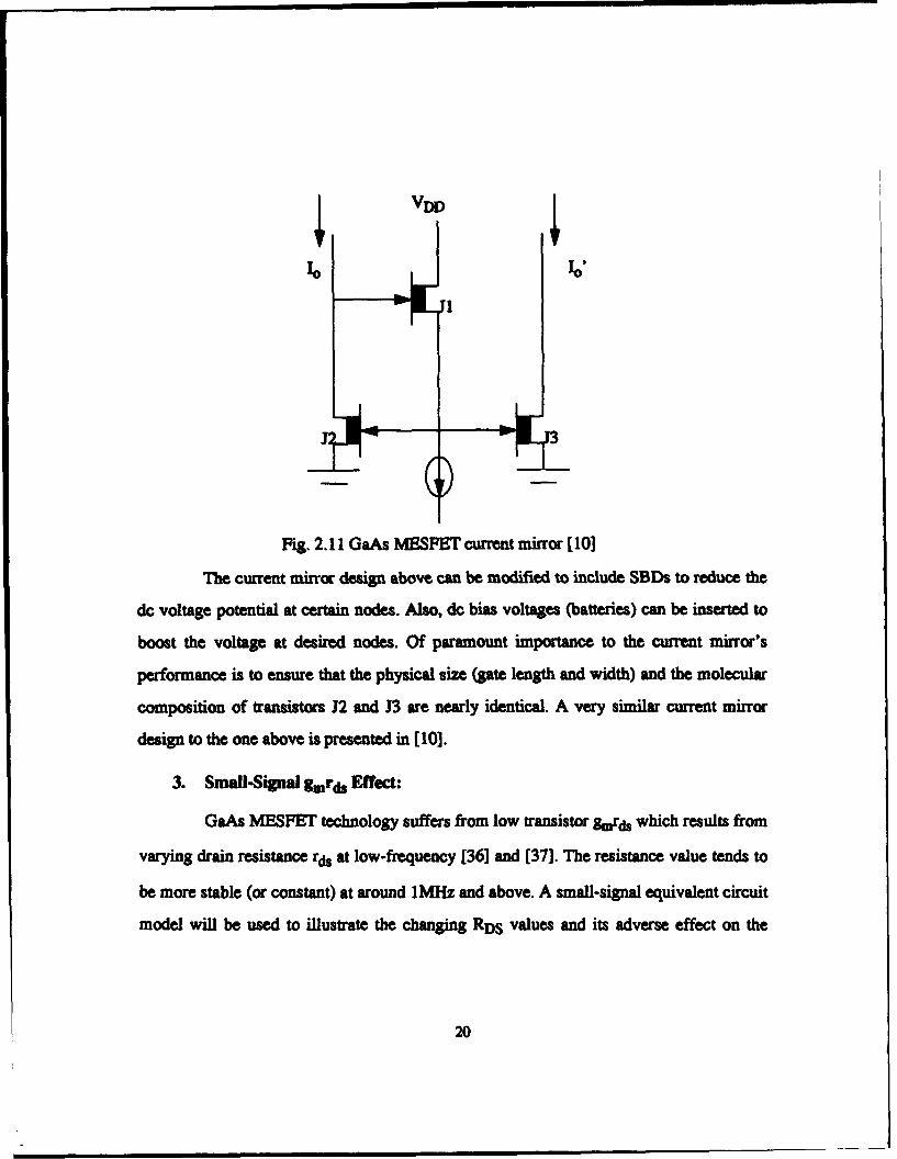
VDD
101
Fig. 2.11 GaAs ME.FET current mirror [10I
The current mirror design above can be modified to include SBDs to reduce the
dc voltage potential at certain nodes. Also, dc bias voltages (batteries) can be inserted to
boost the voltage at desired nodes. Of paramount importance to the current mirror's
performance is to ensure that the physical size (gate length and width) and the molecular
composition of transistors 12 and J3 are nearly identical. A very similar current mirror
design to the one above is presented in [10].
3. Small-Signal gmrds Effect:
GaAs MESFET technology suffers from low transistor gmrds which results from
varying drain resistance rds at low-frequency [36] and [37]. The resistance value tends to
be more stable (or constant) at around IMHz and above. A small-signal equivalent circuit
model will be used to illustrate the changing RDS values and its adverse effect on the
20
system's performance. A signal analysis of Figure 2.12 below will reveal a voltage gain
given by equation 2.13:
-- = -g.(RDI ro) (EQ:2.13)
VgS
where the negative sign indicates that the output signal at vd (the drain terminal)
is 1800 out of phase with the input signal vgs. Another salient point about equation 2.13 is
that as ro becomes small and gm remains large, the value RD will become negligible. Thus,
equation 2.14 shows the new relationship that can be derived from Figure 2.12
Av = -gmro (EQ:2.14)
A general expression and explanation of ro can be found in [6]. A generic small-
signal equivalent GaAs MESFET model is shown:
Gate rgCgd Drain
r i • -C °
rs
Fig. 2.12 Typical small-sig-ni erjuivalent GaAs MESFEr model [9]
Carefully treating (w/ molecular beam epitaxy) and constructing the active
channel layer of the depletion-mode N-channel device will significantly enhance insulating
properties and low-frequency gmrds and reduce backgating and light sensitivity [9]. An
21

acceptable value for the resistance R& should be stictly monitored and obtained at each
stage. For MESFET technology, the output resistance ought to be around 20Q. Achieving
this resistance is a 'tricky' and challenging procedure for analog circuit designers. Figure
2.13 represents the varying drain resistance as a function of frequency.
R jS
15k-
OHMS
(0l)
3k
UENCY (f)
Fig. 2.13 MESFET output resistance vs. frequency [10]
The curve clearly shows the degree of variance of the value R& at low-frequency,
and that the resistance settles to a constant value at approximately IMHz. This behavior of
the MESFET drain resistance is also reported in [9], [10], [38], and (39]. Better
environmental control measures and elaborate modelling techniques have significantly
raised the value of gmrds. In recent years, several methods have been developed to improve
or eliminate the undesirable effects of varying drain resistance at low-frequency,
backgating, and low-light sensitivity [9], and [17].
4. Gain Enhancement Techniques:
This section covers techniques often used to improve FET gain and overall FET
performance in IC designs. Many of the models and configurations presented were
originally developed for MOSFET applications but have been adapted for GaAs MESFET
IC technology.
22

a GaAs DfereL Ampl•er Pair:
The differential amplifier stage is the fundamental building block of analog
VLSI design and operational amplifiers. Differential amplifiers are frequently used in
comparators, multivibrators, logic gates, operational amplifiers, A/D converters, etc.
Currently, there are several GaAs MESFET differential amplifier topologies available.
References [3], [61, [9), and [10] provide instructional techniques for the construction of
such amplifiers. In Figure 2.14, a general purpose depletion mode GaAs MESFET
differential amplifier is shown. Design considerations for a high performance and high
VDD
+ ~VIN_
VTOJ- J2 J9
J vout
VSS
Fig. 2.14 Depletion-mode GaAs Differential Amplifier [40]
yield differential amplifier stage must include bandwidth, common-mode range, common-
mode rejection, and input-offset voltage requirements. This particular differential amplifier
has exhibited a gain bandwidth product of approximately 4MHz and an average gain of
22dB under typical IC applications. Explicit design techniques and methodology
23

concerning this amplifie is contained in [4], [6], [12], and [40]. The topology used in the
amplifier design of Chapter M is very simila to the one in Figure 2.14 above.
b. Curet Source MoedL
The current source is one of the most basic designs of integrated-circuits,
providing both active loads and biasing requirements. Improved amplifier gain can be
accomplished by appropriately adjusting the gate length and width. The current source
circuit can be employed by connecting the gate terminal of the depletion-mode MESFET
to the source terminal. So long as vDS is kept above IV,, the MESFET will operate in the
saturation region and the standard expression for iD is applicable. A current source and its
equivalent circuit design are shown in Figure 2.15 below:
24

VDD +
0 VDS
(a)
(b)Fig. 2.15 (a) M_.FET current source connectedto positive power supply; (b) equivalent circuitof current source
Refer to previous discussions and references concerning the relationship for ro
and iD in the network above. In most IC applications, the gate width of the current source
is reasonably small, as compared to the gate width of the source follower.
c. GaAs Cascode Current Source:
The cascode current source model is a design used primarily to increase the
output resistance Ro of the current source circuit. The effects of incorporating a second
transistor to the current source is define by:
Ro= gM2 ro2rOj (EQ:2.15)
25

A simple circuit analysis of Figure 2.16 shows the output resistance of the current
source component of J I is scaled by gmr02 , the small-signal gain of J2. Typically, the scale
J2
JI
-Vss
Fig. 2.16 GaAs cascode current source
value ranges from 20 -50 in GaAs devices. Additionally, a design requirement for VBiss is
for the voltage potential to be the smallest possible that will maintain the saturation
operation of J2. This will allow for a larger voltage range at the output of the cascode
current source. This technique is frequently employed in GaAs MISFET integrated circuit
designs [11] to boost the voltage gain.
d. Bootstrpfng Current Source:
Much like the cascode current source, the MESFET bootstrapping current
source is another circuit often used to increase the output resistance of a current source.
However, the complexity of the circuit implementation and its design makes it a less
attractive model. The major idea behind this method is to induce an incremental voltage at
the node of the current source A in Figure 2.17, which will cause a corresponding
26
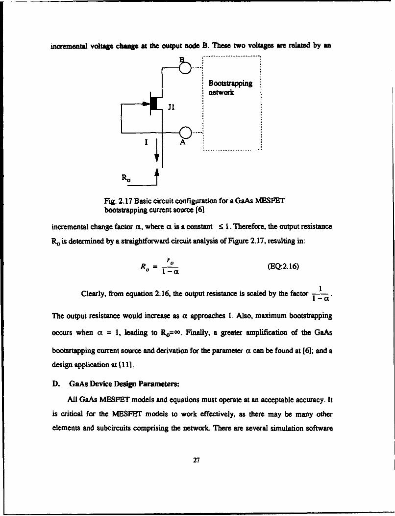
incremental voltage change at the output node B. These two voltages are related by an
Bootstrappingnetwork
I A
Fig. 2.17 Basic circuit configuration for a GaAs MESFET
bootstrapping current source (6]
incremental change factor a, where a is a constant • 1. Therefore, the output resistance
Ro is determined by a straightforward circuit analysis of Figure 2.17, resulting in:
R 1-a (EQ:2.16)
1
Clearly, from equation 2.16, the output resistance is scaled by the factor 1-"
The output resistance would increase as a approaches 1. Also, maximum bootstrapping
occurs when a = 1, leading to Ro=oo. Finally, a greater amplification of the Ga9s
bootsrtapping current source and derivation for the parameter a can be found at [6]; and a
design application at [ 11].
D. GaAs Device Design Parameters:
All GaAs MESFET models and equations must operate at an acceptable accuracy. It
is critical for the MESFET models to work effectively, as there may be many other
elements and subcircuits comprising the network. There are several simulation software
27
tools available, each with slightly different design parameter values. HSPICE was the
simulation software used to simulate the amplifier of Chapter III. HSPICE is extremely
accurate, and provides an excellent Graphical Simulation Interface (GSI) module. The GSI
tool renders the simulation output under a separate file catalog, making it easier for the user
to view, update the file, and to print necessary results. See references [3] and [8) for other
design models and simulation tools.
Additionally, HSPICE employs the Vitesse corporation gallium arsenide MESFET
design models and parameter values. The construction of both the GaAs schottky-barrier
diode and transistor were previously discussed. Furthermore, changes to the Vitesse model,
parameter values, and creation of new parameter values were prohibited, due to future
design layout and fabrication requirements. That is, the only user design parameter
flexibility allowed was to alter the devices gate length and width. The Vitesse MESFET
model parameters are shown below for the gate capacitance and DC model, and the
temperature effect parameters in Tables 2.3 and 2.4 respectively.
TABLE 2.2: Gate Capadtance and DC Model Parameters
Name Parameter Unit Vitesse Default
CAPOP Cap. option F 1.0 0
CGAMDS Threshold F 0.065 0lowering
factor cap
CRAT Source frac- F 0.666 0.666tion gate
cap.
GCAP Zero-bias F 1.7e-3
gate cap.
BETA Gain amp/V2 1.9e-4 1.0e-4
LAMBDA Channel I/V 0.065 0length mod.
28

TABLE 2.2: Gate Capacitance and DC Model Parameters
Name Parameter Unit Vitesse Default
VTO Threshold V -0.825 -2.0voltage
LEVEL FET level mrA 3 1
ALPHA Sat. factor I/V 3.5 2.0
D Dielectric Si=11.7 11.7constant GaAs= 10.9
K1 Threshold V2 0.350 0voltage sens
ND Drain fact IN 0.2 0
NG Gate fact. 1.1 0
SAT Sat. factor 3 0
SATEXP Drain volt- 3 3age exp.
UCRIT Critical V/cm 0.5 0field
VGEXP(Q) Gate exp. 2 2
TABLE 2.3Temperature Effect Parameters
Name Parameter Unit Vitesse Default
BEX Mobility -0.4 0temp coeff.
EG Energy gap ev Si=1.17 1.16SBD=0.69Ge--0.67
GaAs=1.52
GAP1 1st bandgap ev/deg Si=4.73e-4 7.02e-4Ge=4.56e-4GaAs=5.41
e-4
29
TABLE 2.3Temperature Effect Parameters
Name Parameter Unit Vitessc Default
GAP2 2d bandgap deg Si=636 1108Ge=210
GaAs=204
TCV Temp comp I/deg 1. 10e-3 0coeff VTO
TLEV Temp eqn 2 0
TRD Temp coeff I/deg 3.3e-4 0drain resist
TRS Temp coef lldeg 3.3e-4 0source resist
XTI Sat current 2 0temp exp
The gate length (L) and width (W) parameters for the device are fixed in the
algorithm so that L and W vary between the ranges 0.4: L ! 1.249911m and
0.5•9 W!< 10000ptm. In order to obtain a different L and W range, a new Vitesse model
number must be selected. HSPICE has three Vitesse GaAs transistor devices of semi-fixed
lengths 1,2, and 3pJm. Vitesse also provides enhancement and depletion-mode MESFETs
at the gate lengths already mentioned. The parameter values listed in Tables 2.1, 2.2, and
2.3 were obtained from the hgaas3.model, depletion-mode 1.1 (dpl.l) of the Vitesse
library. Specific equation derivations and relationships can be found in reference (43] Meta
Software.
30

mL GaAs MESFET OPERATIONAL AMPLIFIER DESIGN
A. General:
The operational amplifier (op amp) is an essential and reliable component in the
electronic technology industry. Op amps were first introduced in the late 1940s. The single
vacuum-tube op amp, invented by G. Philbrick [51, was one of the first op amp circuits
published. These initial op amps were extremely large (in size), expensive, and performed
only simple mathematical computations.
It wasn't until almost two decades later that solid-state technology (transistors) made
their way onto the scene. In the mid-to-late 60's, Fairchild perfected the now famous LM-
741 integrated circuit op amp. This breakthrough in the electronics industry lead to
remarkable strides in the computer and engineering sciences. The solid-state integrated
circuit technology had taken root by the mid 70's, and new advancements in the field were
rapidly coming to fruition. Additionally, the op amp was exceedingly more robust than its
predecessor. It was physically smaller, less expensive, easier to work with, and far more
capable than vacuum tube op amps.
The IC op amp became a major building block for more complicated designs.
Engineers were able to get away from the rudimentary tasks of designing multiple discrete
component subcircuits to achieve a particular performance level. A new and more powerful
circuit (chip) can be designed from just an op amp, a few capacitors, and resistors. Today,
op amps are readily available in a wide range of specifications, applications, and physical
properties. The op amp is very simple to use and it operates closely to its ideal
characteristics.
This Chapter will mainly focus on the GaAs MESFET operational amplifier design. A
step-by-step design and a completed schematic of the op amp is included. Circuit Models
and gain improvement techniques for the op amp will be covered as well. Most of the
design parameters and specifications are labelled on the diagrams. Lastly, problems
31
inherently associated with GaAs op amps will be highlighted, such as: low gain, slew rate,
offset voltage, etc.
B. GaAs Differential Amplifier Input Gain Stage:
The differential amplifier stage is probably the most critical subcircuit of an
operational amplifier. The differential amplifiers' high input resistance and low output
resistance renders it quite useful in the design of logic gates, multivibrators, op amps, etc.
The GaAs depletion-mode MESFEr op amp pictured in Figure 3.1 is the design topology
closely followed in the construction of the final amplifier for this study. Specific
VDD
i
D J4
VI-N
VINs
Fig. 3.1 GaAs D-MESFET operational amplifier [4]
dimensions and explanations of all the elements in Figure 3.1 can be reviewed in (4]. This
32
medium dc gain and bandwidth amplifier is suitable for moderate rate switched-capacitor
filters, phase-locked loop, and other medium high speed analog applications. Experimental
and simulation results of the above op amp are contained in Table 3.1 below:
TABLE 3.1: Op Amp Performance Parameters [41
Parameter Value Unit
dc gain 40 dB
GBWP 1.3 GHz
Phase mar- 80 Deggin
Power dissi- 150 mWpation
Offset volt- 63 mVage
Load capac- 0.4 pfitance
GaAs op amps possessing improved performance over the one mentioned here have
been developed and are available. Such amplifiers can be seen in references [9], [10], [11],
and [19]. The performance of the amplifier used in this thesis is not as great as the amplifier
in Figure 3.1, still it is more than adequate for composite op amp exploration. Table 5.1
contains the key op amp performance parameters for the op amp designed in this thesis.
In wide bandwidth switching applications, as in high frequency switched-capacitor
filter designs, it has been shown that a single-ended single-stage op amp is best [41].
Consider the equivalent circuit model of the single-stage and two-stage op amps in Figure
3.2. In this case, the gain for both models are about the same and is given as:
gain = (gmrd,) 2 (EQ:3.1)
Now, notice that the two-stage amplifier's non-dominant pole location is given by:
33

(CL 2 (EQ:3.2)
and the single-stage amplifier's non-dominant pole location is defined by:
C--Q2 (::3.3)
This is a potentially wider bandwidth than the two-stage op amp. Accodingly, the
non-dominant pole plays a key role in the maximum obtainable bandwidth of an op amp
34

(4]. Additionally, the single-stage op amp is intrinsically much more robust and increases
the load capacitance compared to the two-stage model. This makes it more stable [42].
Vcdd
Vin
(a)
Vdd
yin C
.' gnd
Vmp (b) V•
Fig. 3.2 Single-ended equivalent circuit model (a) two-
stage (b) single-stage op amp [4]
The discussion above is intended to provide insight on the design models for higher
frequency GaAs op amps. However, these models are more complex to implement and will
not be employed in the final op amp design.
The final amplifier incorporates forward biased SBDs for level-shifting. Additionally,
the high series resistance of the SBDs moderately reduce the amplifier gain. Thus, a careful
design strategy must be used when building the level-shifters. The differential amplifier
35
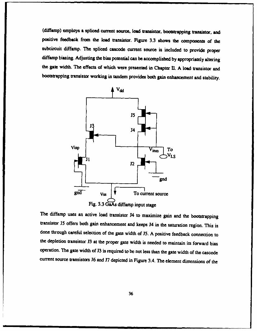
(diffamp) employs a spliced current source, licd transistor, bootstrapping transistor, andpositive feedback from the load transistor. Figure 3.3 shows the components of thesubcircuit diffamp. The spliced cascode current source is included to provide properdiffamp biasing. Adjusting the bias potential can be accomplished by appropriately alteringthe gate width. The effects of which were presented in Chapter II. A load transistor andbootstrapping transistor working in tandem provides both gain enhancement and stability.
gnTd
- -J-VL
gna Vss TO Current source
Fig. 3.3 diffamp input stage
The diffamp uses an active load transistor J4 to maximize gain and the bootstrapping
transistor J5 offers both gain enhancement and keeps J4 in the saturation region. This isdone through careful selection of the gate width of J5. A positive feedback connection tothe depletion transistor J3 at the proper gate width is needed to maintain its forward biasoperation. The gate width of J3 is required to be not less than the gate width of the cascodecurrent source transistors J6 and J7 depicted in Figure 3.4. The element dimensions of the
36
diffamp are based purely on FEr design tchniques, simulations, and MOSFET equivalent
circuit modelling. These element dimensions are given in Table 3.2
TABLE 3.2: diffamp Element Dimensions
FEr # Gate width Multiplier
1&2 2000 1
3 700 1
4 50 1
5 1500 1
6&7 15 1
8&9 1.0 1
10 110 1
11 2 1
DI -D3 1.5 15
D4 -D7 1.5 20
FEs J6 - Jl I and DI - D7 are shown in Figure 3.4 below. A GaAs D-FET model with
a gate length of 0.8g±m was used for all FETs. Also, the diode gate length was set at 0.Sim.
The gain for the input diffamp was found to be approximately 21.44.
C. Load Stage and Complete Op Amp:
A series of four forward biased SBDs are used to provide the necessary level-shifting
network. The current through these SBDs is kept to a nominal level via the small gate width
37
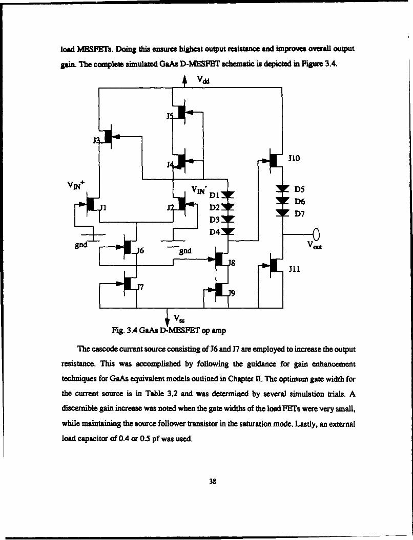
load MESFTs. Doing this ensures highest output resistance and improves overall output
gimn. The complete simulated GaAs D-MESFET schematic is depicted in Figure 3.4.
Vdd
J1o
VINl D5
1 D2 D6
D3 D7
D4gnd--76gdVu
Fig. 3.4 GaAs D-MEFET op amp
The cascode current source consisting of J6 and J7 are employed to increase the output
resistance. This was accomplished by following the guidance for gain enhancement
techniques for GaAs equivalent models outlined in Chapter 11. The optimum gate width for
the current source is in Table 3.2 and was determined by several simulation trials. A
discernible gain increase was noted when the gate widths of the load FETs were very small,
while maintaining the source follower transistor in the saturation mode. Lastly, an external
load capacitor of 0.4 or 0.5 pf was used.
38

D. Op Amp Drawbacks:
The ideal op amp performance characteristics can never be achieved by any non-ideal
op amp. Because these performance characteristics have been well documented in other
publications, it is not necessary to present all of them here. On-the-other hand, this
paragraph will focus on a few drawbacks associated with non-ideal op amps.
The ideal op amp possesses infinite input impedance, zero output impedance, and
infinite output voltage gain. However, the non-ideal op amp is hindered by finite dc gain,
common-mode rejection ratio, offset voltage, limited bandwidth, slew-rate, finite input
impedance, and nonzero output impedance. These topics are pertinent to the overall
performance of the op amp. A more exhaustive look at these drawbacks are found in [3],
[6], and [28].
1. Finite DC Gain:
As stated above, an ideal op amp possess infinite dc gain, but a non-ideal op amp
generally has a finite range of 1000 to more than 1-Meg. for silicon type devices. Yet, for
GaAs MESFET op amps, the dc gain range is significantly less, around 100 to 1000.
2. Common-Mode Rejection Ratio:
The common-mode rejection ratio (CMRR) of an op amp is defined by:CMRR = 2og ( IAI (EQ:3.4)
iaOlo o EQ:3.4
where A is the input signal differential gain and ACM is the common-mode gain.
The CMRR value is indirectly related to frequency, in that it decreases as the frequency
increases. So, in silicon, a typical range for CMRR is 70 to 110 dB for low frequency, and
in GaAs, approximately 40 to 60 dB.
3. Offset Voltage:
A general-purpose op amp offset voltage is given as the differential input voltage
needed to force the differential output voltage to zero. Thus, when the inputs of a non-ideal
39

op amp are connected together, a small voltage potential appears at the differential inputs.
This voltage potential is amplified at the output. This effect can almost be negated by
applying the appropriate offset voltage at the input. It is worth noting that for ideal op amps
where the inputs have been connected together, the corresponding output voltage is zero.
4. Effective Bandwidth:
Op amps have reduced available gain across the bandwidth (BW). This reduction
in available BW is cause by parasitic capacitances and limited carrier mobility. The
problem gets worse as the frequency increases. Also, internally capacitively compensated
op amps have a 20 dB roll-off cause by the induced poles from the internal capacitors.
Lastly, ideal op amps have infinite gain over the complete BW.
5. Slew-Rate:
The slew-rate (SR) of an op amp indicates the maximum speed at which the
output voltage can change. Equation 3.5 is an analytical expression for the SL. The slew-
rate is affected by several factors, including component values, input voltage swing, gain,
dc supply voltages, etc.
dv 0SR = --t max (EQ:3.5)
In most cases, the output of the op amp is 1-volt below the positive and negative supply
rails.
6. Input and Output impedances:
A general-purpose op amp has finite input impedance in the neighborhood of 10
-20 MK. Conversely, the ideal op amp has infinite input impedance.
Briefly, op amps do not exhibit zero output impedance. If this were the case, op
amps would operate as an ideal voltage source. Therefore, ICs are frequently designed with
buffer stages that have low output resistance in the range of several hundred ohms.
40

IV. COMPOSITE OPERATIONAL AMPLIFIERS
A. General:
Composite Operational Amplifiers (CNOAs) were developed to extend the effective
frequency range of a single op amp, and to reduce some of the drawbacks mentioned in the
previous chapter. This is accomplished by using a multiple op amp configuration. In an op
amp, the gain bandwidth product and the 3dB frequency are constants. Furthermore, the
performance parameters of bandwidth and distortion are not readily controlled when using
a single op amp. However, to a certain degree, this has been overcomed and the bandwidth
extended through the use of CNOAs.
The CNOA concept was developed in 1981 by S. Michael and W. Mikhael. Their
research concentrated on extending the operational frequency of a single op amp and is
based on the nullator and norator pairings of some 136 different circuit designs. Each
circuit design was evaluated against the performance requirements outlined in [43]. Since
CNOAs are not being simulated, only a brief discussion will be devoted to these designs.
B. Theory Behind CNOAs:
The fundamental operational characteristics of an ideal op amp are infinite input
impedance, zero output impedance, and infinite gain. These characteristics can directly be
transferred to an idealized model with the use of nullator and norator singular components
[1] and [431. A nullator is a one port device that does not sustain a voltage nor passes a
current. On-the-other-hand, a norator is a one port device that sustains an arbitrary voltage
41

and paase an arbitrary independent current [43] and [451. Both the nullator and norator
along with the hybrid nullor op amp are pictured in figure 4.1.
Vl--1 1=Of iiVI
(a) NuUator
V2 i2 arbitrary
i2
'12
(b) Norato"
42

zi -+ 0, Zout -+. 0, A --+ co
10
(c) Nullor op amp (VCVS)Fig. 4.1 (a) Nullator (b) Norator (c) Nullor op amp
The nullor op amp of figure 4.1c is the re. At of applying a nullator-norator analysis
technique. From this analysis spurred the creation of 136 CNOAs. The number of CNOAs
were reduced to just four, because the others did not meet the performance requirements
listed in reference [43). These four were redesignated as CNOA-1 through CNOA-4, where
N=2. The new composite nullor device symbol is very similar to an ordinary single op amp
with external input and output terminals.
Equation 4.1 defines the open-loop gain of the single pole op amps used in the C2OAs.
These op amps are shown in there composite form at figure 4.2.
Aoioii COiAi -9- 1 = lor2 (EQ:4.1)
co0+S + CDLi
where Aoi, Cow, and coi are the dc open-loop gain, 3dB bandwidth, and the gain
bandwidth product (GBWP) of the ith single op amp, respectively. Additionally, the input-
output voltage relationship of the C2OA-i's are given below:
"43
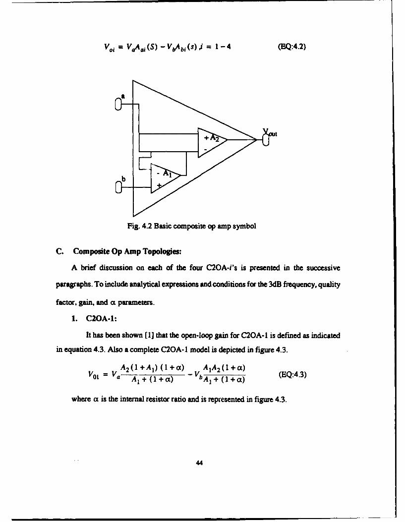
Voi = Va.a (S) - V A bi (s) = I - 4 (EQ:4.2)
9--
Fig. 4.2 Basic composite op amp symbol
C. Composite Op Amp Topologies:
A brief discussion on each of the four C2OA-i's is presented in the successive
paragraphs. To include analytical expressions and conditions for the 3dB frequency, quality
factor, gain, and a parameters.
1. C2OA-I:
It has been shown [I] that the open-loop gain for C2OA-I is defimed as indicated
in equation 4.3. Also a complete C2OA-I model is depicted in figure 4.3.
A2 (1 +A,) (l+a) AIA 2 (l +a) (EQ:4.3)SAl + ( 1 ÷+a) -WAl +4 (I +a O)
where a is the internal resistor ratio and is represented in figure 4.3.
44

a Vout
C2bA
Fig. 4.3 C2OA-l model
Notice the striking resemblance of the three terminal composite op amp of figure 4.3
to that of a single op amp. Inputs a & b are the noninverting and inverting terminals
respectively. A thorough derivation of the 3dB frequency and the quality factor (Q) for the
model above are found in [1] and [2]. An expression for these parameters are given as:
/o ••• (EQ:4.4)
(1 + a) •2(Q45
(l-j-]+k) (CQ4.5
where a is the internal resistor ratio, o is the 3dB frequency, k is the closed-loop
gain, and o1& co2 are the GBWP for A1, and A2 respectively. The system's stability
45

conditions are validated by applying the Routh-Hurwitz criterion, and the resulting
relationship is provided:
(1+ a) <1 +A (EQ:4.6)
2. C2OA-2:
The open-loop voltage gain for C2OA-2 is defined as indicated in equation 4.7.
Also, a complete C2OA-2 model is depicted in figure 4.4.
V A 1A 2 (0 +a) A 1A 2 (1+a) (EQ:4.7)
V A + -(1 +a) VA2+ (1 +a)
where ct is the internal resistor ratio and is represented in figure 4.4.
The 3dB frequency and the Q factor for C2OA-2 are given below:
2 (EQ:4.8)
QP (l+k) (EQ:4.9)
The Routh-Hurwitz conditions for system stability are given at equation 4.10
below:
(I+ a) < 1+k (EQ:4.10)
"46

3. C2OA-3:
The open-loop voltage gain for C2OA-3 is defined as indicated in equation 4.11.
Also, a complete C2OA-3 model is depicted in figure 4.5.
A 1A 2 A 2 (1 +A 1)(E:.1
A l V1u2
V0 V 1 )(+ a)
Qp A2 (E:.3
wher isen-loop internalgresistorfrao a is reprented asindfigured 4.5. quat
The 3dB frequency and the Q factor for C2OA-3 are given below:
(OP (1 OaI(1+k (EQ:4.12)
(1+k (02~ w (EQ:4.13)
47

The Routh-Hurwitz conditions for system stability are given at equation 4.14
below:
(I+ +x) > J-1 + k (EQ:4.14)
bvo
b +
Fig. 4.5 C2OA-3 model
4. C2OA.4
The open-loop voltage gain for C2OA-4 is defined as indicated in equation 4.15.
Also, a complete C2OA-4 model is depicted in figure 4.6.
A2 (A,+ a) A2 [AI + (I + a) (EQ:4.15)V = Va (1+ a) Vb (1 +a)
where a is the internal resistor ratio and is represented in figure 4.6.
The 3dB frequency and the Q factor for C2OA-4 are given below:
48

CP = (EQ:4.16)
(I + k) CO(O +a) w2
(EQ:4.17)
The Routh-Hurwitz conditions for system stability are given at equation 4.18
below:
(1 +a) >4(l +k) (EQ:4.18)
b vu
Fig. 4.6 C2OA-4 model
It is worthwhile to point-out that the expressions for a~p, Qp, and the Routh-
Hurwitz criterion are a function of the parameters a and K. These two parameters also play
a key role in implementing a high performance composite op amp. This is described in the
49
i~ a: I+ l lllll i~l

next paragraph. A more detailed and in-depth look at the generation of composite op amps
is found at [1], [2], [43], [44], and [45].
D. Determining Appropriate a and K Parameter Values:
In the composite op amp configuration, the designer has much the same control of the
closed-loop gain K, as in a single op amp. Once a K value has been chosen, the
corresponding 3dB frequency and quality factor can be computed. Likewise, the a
parameter is selected by the designer and should be adjusted until the frequency response
curve of the composite op amp is maximally flat. Proper and accurate implementation of
anyone of the four C2OAs will result in a stable system, as established from the Routh-
Hurwitz criterion previously manifested and references [1] and [2].
E. Greater Bandwidth Using C2OAs:
Probably the most significant performance characteristic of the C2OAs is their
intrinsic capacity to extend the operational frequency of a given single op amp. In a single
op amp configuration, the bandwidth is reduced by a quantity of 1/k. Also, its been
documented that cascaded op amps have a bandwidth reduction factor of approximately
0.66 Alternatively, C2OAs' GBWP can be designed to achieve a smaller shrinkage (as1k1
compared to the two previous op amp configurations) roughly I for Qp = 0.707, which
is maximally flat [44]. Thus, the composite op amp makes better use of the available
bandwidth than the single or cascaded op amp.
F. C2OAs Component Sensitive:
The composite op amp design is less sensitive to fluctuations in both active and
passive components (2]. Consider, C2OAs' general transfer function shown below:
50

T~s) = 1 + as
T(s) +as (EQ:4.19)I + blS + b2s2
where b, is defined:
1b Q (EQ:4.20)
and b2 is defined:
b (EQ:4.21)
From the relationships above, it is obvious that neither the a nor the b coefficients are
attained by way of difference equations. This precludes the requirement for single op amps
with identical GBWPs, thereby lowering the sensitivity of C2OAs, [2] and [43].
G. Offset Voltages:
All general-purpose op amps have a small differential input voltage between the
noninverting and inverting terminals. This differential input voltage is known as the input
offset voltage. Its corresponding amplification (caused by gain of the op amp) at the output
is called the output offset voltage. If the effects of the offset voltage are not kept to an
absolute minimum it could cause a degraded signal at the output. As with single op amps,
the composite op amp suffers from differential input offset voltage too.
The composite op amp offers a crafty technique for mitigating the effects of
differential input offset voltage. This is accomplished by selecting an op amp A,, that has
a small offset voltage and an op amp A2, that has a relatively high slew-rate. The benefit of
this technique on C2OAs can best be assessed by viewing the definitions for the differential
offset voltages listed in Table 4.1.
51

TABLE 4.1: C20A Input Offset Voltage
C2OAs input Offst voltages
C2OA-1 Voe =Van + (VY / a)
C2OA-2 Vf =V•Ij + (V•[ / A,)
C2OA-3 VOH -=VOM + (Vom (I + a)/A,)
C20A-4 Vf =v00 + (VOW (I + a)/A l )
Observe from Table 4.1 above, the input offset voltage Vff is virtually independent
of VMfD (input offset voltage for op amp A2), but is heavily dependent on V 1ffl (input offset
voltage for op amp A,). Subsequently, in C2OA-1, as a is made large, the voltage V.0j2
has practically no influence on Vaif. Moreover, in the other C2OA expressions, V.0 is
scaled by the value 1/A1. Since the open-loop gain is always very high, the effects of V.0l
is negligible. Neutralizing the adverse effects of the input offset voltages, coupled with the
fast slew-rate of A2, makes the composite op amp design extremely intriguing.
H. C2OA Slew-Rate Considerations:
Most general-purpose op amps are designed to have either a fast slew-rate (SR) or a
small offset voltage. Alternatively, a composite op amp makes maximum use of both of
these qualities by employing an op amp with a small offset voltage at A1, and an op amp
with a fast SR, wide bandwidth, and fast settling time at A2. Finally, composite op amps
properly designed and implemented vastly out perform any single op amp.
52

V. SIMULATION RESULTS
A. General:
The GaAs op amp described in Chapter MII was simulated in both the open and closed
loop modes. The results are presented in this Chapter.
B. Power Supply:
The power supply voltages used in the simulation are selected to accommodate the
largest desired input signal swing. For the op amp under test, the values for Vdd and Vss
were +7.0 and -7.0 volts respectively.
C. Establish Finite Gain:
A closed-loop gain of k=10 was simulated. This was accomplished by selecting Rj=
6200 and Rf = 62000. This gain is sufficient for testing the design and validating the
circuit's functionality.
D. Open-Loop Analysis:
The open-loop circuit simulation was performed many times to verify the validity of
the design. Input signals of 10mV and 100mV were applied to the circuits of Figures 5.1
and 5.2 respectively. An input offset voltage of 20mV was applied. A load capacitor of
0.4pF was used in each case. Notice that for each curve the unity gain frequency is
approximately 3.0GHz. This unity gain bandwidth is typical of GaAs op amps. The GaAs
op amps at references [4], [9], and [10] have similar gain and bandwidth. However, as
expected, the low-frequency gain was as measured at 32dB.
53

OPEN-LOOP. VII4.IOHV. CLt.o4
Vogt Is.12. O
. .. . . .....
-5.5w..................... ........................ .... ..............
10..00 0 .0 .. O ......... f0 0 .........c.KiET LG 00
........... g..... ....1 O pen-loop .......... respon....e ........ ..........
-26.54

OPEN-LOOP. VIN.IOONV. CL0.OAPF
VOG C
V27 50 .........:
0L -10 0T
o 12 .50
L -27 .50
-320. 0 ...............................
-37 .50 ............................
-25.0

CLOSCO-LOOP. yIN. DOPEY
14 c) ............... ................. .............................................. ............. ...... _ V U
V......... .. .. ......
!II *1 .0 .
9z
.. . . . . . . . ... . . . . . . . . . . . . . . . . . . . .. . . . . . . .
-20.0 7
L i . . . . . . . . . . . . . . . . . . . . . .
-2.I
N 2.1 00 0.K 1O1 . 0. . . . . . . .. . . ... .. . . .. . . . ... ... .. ...... .. .....
-20. ~ ~ ig 5. Cltd l o re po s -------- 10)... ........... ......... .. ............
567

E. Closed-loop Analysis:
The closed-loop frequency response of the op amp is shown in Figure 5.3, for K=lO.
The 3dB frequency is approximately 400MHz. This value is better than anticipated,
because an op amp's gain-bandwidth is a constant. Again, the power dissipation for this
circuit was about 135mW.
TABLE 5.1: Op Amp Performance Parameters
Parameter Value Unit
dc gain 32 dB
GBWP 3.0 G-z
Phase mar- 135 Deggin
Power dissi- 135 mWpation
Offset volt- 83 mVage
Load capac- 0.4 pfitance
Finally, Table 5.1 provides a summary of the GaAs op amp's key performance
parameters.
57

VI. CONCLUSIONS AND RECOMMENDATIONS
A. Condusions:
This research has demonstrated that a general-purpose op amp can be designed using
the Vitesse GaAs MESFET process. The performance of the op amp is more than sufficient
for composite operational amplifier implementations. The design appears quite stable and
should be useful in most high speed applications.
Composite op amps can mitigate the limiting effects of input offset voltage, slew-rate,
and reduced operational frequency commonly found in a single op amp. By carefully
selecting an op amp with a small input offset voltage for Al, and an op amp with a high
slew-rate for A2 , a composite op amp circuit can be constructed that has significantly
improved performance compared to a single op amp.
B. Recommendations for Future Research:
There are many ancillary studies that can be initiated as a result of the findings in this
paper. Some of which are listed in the following paragraphs:
1). Design and test the discrete components of the GAs op amp.
2). Implement the op amp in the design of a composite operational amplifier (CNOAs).
3). Design and fabricate the composite op amp.
4).Determine whether the op amp can be employed in a switched-capacitor network.
6). Revisit the ground level concept of composite operational amplifier generation as
it pertains to GaAs MESFETs. In particular, those issues surrounding the low frequency
gain and open-loop unity gain frequency.
58

LIST OF REFERENCES
1. Mikhael, W. B., and Michael, S., "Composite Operational Amplifiers: Generationand Finite-Gain Applications," IEEE Transactions on Circuits and Systems, v.CAS-34, No. 5, pp. 449-460, May 1987.
2. Mikhael, W. B., and Michael, S., "Inverting Integrator and Active FilterApplications of Composite Operational Amplifiers," IEEE Transactions onCircuits and Systems, v. CAS-34, No. 5, pp. 461-470, May 1987.
3. Long. S. I., and Burner, S. E., Gallium Arsenide Digital Integrated Circuit Design,McGraw-Hill Series in Electrical Engineering, 1990.
4. Larson, L. E., Gallium Arsenide Switch-Capacitor Circuits for High Speed SignalProcessing, Ph. D. Dissertation, UCLA 1986.
5. Coughlin, R. F., and Driscoll, F. F., Operational Amplifiers and Linear IntegratedCircuits, 4th ed., Prentice Hall, 1991.
6. Sedra, A. S., and Smith, K. C., Microelectronic Circuits, 2d ed., Holt, Rinehart andWinston, Inc., 1987.
7. Schaumann, R. S., Ghuasi, M. S., and Laker, K. R., Design of Analog FiltersPassive and Active RC, and Switched Capacitor, Prentice Hall, 1990.
8. Soares, R., Graffeuil, J., and Obregon, J., Applications of GaAs MESFETs, ArtechHouse, Inc., 1983.
9. Larson, L. E., Chou, C. S., Deakin, D. S., Hooper, W. W., Jensen, J. F., Thompson,M. A., Delaney, M. J., McCray, L., Rosenbaum, S. E., and Pierson, D. A., "A10GHz Operational Amplifier in GaAs MESFET Technology," IEEE TransactionsInternational Solid-State Circuits Conference, Digest of Technical Papers, pp. 72-73, Feb., 1989.
10. Scheinberg, N., "High-Speed GaAs Operational Amplifier", IEEE Journal ofSolid-state Circuits, Vol. SC-22, No. 4, August 1987.
11. Visocchi, P. M., Taylor, J. T., Betts, A. K., and Haigh, D. G., "The Variable GainBootstrap Active Load: A New Approach to Amplifier Voltage Gain Enhancementand Control," IEEE Transactions on Circuits and Systems-I, Fundamental Theoryand Applications, Vol. 40, No. 7, pp. 440-448.
12. Larson, L. E., Jensen, H. M., Levy. H. M., Greiling, P. T., and Temes, G. C., "GaAsDifferential Amplifiers," IEEE GaAs Symposium, pp.19-22, 1985.
59

13. Larson, L. E., "An Improved GaAs MESFET Equivalent Circuit Model for AnalogIntegrated Circuit Applications," IEEE Journal of Solid-state Circuits, Vol. SC-22,No. 4, pp. 567-574, August 1987.
14. Snowden, C. M., and Pantoja R. R., "GaAs Physical Models for Process-OrientedDesign," IEEE Transactions of Microwave Theory and Techniques, Vol 40, No. 7,pp,. 1401-1409, July 1992.
15. Jain N., and Gutmann R. J., "Modeling and Design of GaAs MESFET ControlDevices For Broad-Band Applications, IEEE Transactions of Microwave Theoryand Techniques, Vol 38, No.2, pp. 109-117, January 1990.
16. Takasu, H., and Yamashita, E., "Impedance Characterization of GaAs FETSwitches," IEEE Transactions of Microwave Theory and Techniques, Vol 40, No.7, pp. 1422-1429, July 1992.
17. McCamant, A. J., McCormack G. D., and Smith, D. H., "An Improved GaAsMESFET Model for SPICE," IEEE Transactions of Microwave Theory andTechniques, Vol 38, No 6, pp. 822-825, June 1990.
18. Harold, S. J., Mun, V. J., and Haigh, D. G., "A GaAs Switched-CapacitorBandpass Filter IC," IEEE GaAs IC Symposium, pp. 23-26, 1985.
19. Haigh, D. G., Toumazou C., Harold, S., J., Stepote, K., Sewell, J., I., and Bayruns,R.," Design Optimization and Testing of a GaAs Switched-Capacitor Filter," IEEETransactions on Circuits and Systems, Vol. 38, No. 8, pp. 825-837, August 1991.
20. Deville, Y, "A High-Selectivity Continuous-Tune GaAs," IEEE Journal of Solid-State Circuits, Vol. 25, No. 3, pp. 899-892 June 1990.
21. Gregorian, R., and Temes, G. C., Analog MOS Integrated Circuits for SignalProcessing, John Wiley & Sons, 1986.
22. Reinhold V. N., Switched Capacitor Circuits, Van Nostrand Reinhold, CompanyInc., 1984
23. Yalkin, C., Digitally Programmable Active Switched Capacitor Filters, MSEE.Thesis, Naval Postgraduate School, Monterey, California, March 1987.
24. Bingham, E. W., Stray Insensitive Switched Capacitor Composite OperationalAmplifiers, MSEE, Naval Postgraduate School, Monterey, California, March 1993.
25. Gray, P. R., and Meyer, R. G., "MOS Operational Amplifier Design- A TutorialOverview," IEEE Journal of Solid-state Circuits, Vol. 17, No. 6, pp. 969-982,December 1992.
60
26. Senderowicz, D., Hodges, D. A., and Gray P. R., "High-Performance NMOSOperational Amplifier," IEEE Journal of Solid-State Circuits, Vol. 13, No. 6, pp.760-766, December 1978.
27. Tsividis, Y. P., Fraser, D. L., and Dziak J. E., "A Process-Insensitive High-Performance NMOS Operational Amplifier," IEEE Journal of Solid-State Circuits,Vol. 15, No. 6, pp. 921-928, December 1980.
28. Gregorian, R., and Temes, G. C., Analog MOS Integrated Circuits for SignalProcessing, John Wiley & Sons, 1986.
29. Gray, P. R., Brodersen, R. W., Hodges, D. A., Kaneshiro, C. R., and Hsieh, K. C.,"Some Practical Aspects of Switched-Capacitor Filter Design," Proc., IEEEInternational Symp. Circuits and Systems, PP. 419-422, April 1981.
30. Miller D., et al., "Low Frequency Oscillations in GaAs IC's," Proc., GaAs ICSymp., pp. 31-34, November 1985.
31. Englemann, R., and Liechti, C., "Bias Dependence of GaAs and InP MESFETParameters," IEEE, Transactions Electronic Devices, Vol. ED-24, pp. 1288-1296,November 1977.
32. Shur, M., GaAs Devices and Circuits, Plenum Press, New York, 1987.
33. Kuan, T. S., Batson, P. E., Jackson, T. N., Rupprecht, H., and Wilkie, E. L.,"Electron Microscope Studies of an Alloyed Au/NiIAu-Ge Ohmic Contact toGaAs," J. Applied Physics, Vol. 54, pp. 6952-6957, December 1983.
34. Sze, S. M., Physics of Semiconductor Devices, 2d ed., Wiley, 1981.
35. Lile, D. L., Metal-Insulator-GaAs Structures, in Gallium Arsenide, (editors, M. J.Howes and D. V. Morgan), Wiley, 1985.
36. Larson, L. E., "Gallium Arsenide MESFET Modeling for Analog IntegratedCircuit Design," IEEE International Symp. Circuit Systems, pp. 1-5, 1987.
37. Scheinberg, N., Bayruns, R., and Goyal, R., "A Low-Frequency GaAs MESFETCircuit Model," IEEE Journal of Solid-State Circuits, Vol. 23, pp. 605-608, April1988.
38. Camacho-Penalos, C., and Aitchison, C., "Modeling Frequency Dependence ofout Impedance of a Microwave MESFET at Low Frequencies," ElectronicsLetters, pp. 528-529, June 1985.
39. Smith, M. et al., "RF Nonlinear Device Characterization Yields ImprovedModeling Accuracy," IEEE MTT-S Digest, pp. 381-384, 1986.
61

40. Mikhael, W. B., and Michael, S., "A Systematic General Approach for theGeneration of Composite OAs With some Useful Applications in Linear ActiveNetworks," Proceedings of the 25th Midwest Symposium on Circuits and Systems,pp. 454-463, Houghton, Michigan, August 1982.
41. Mikhael, W. B., and Michael, S., "High-Speed, High Accuracy CompensatedComposite Operational Amplifiers," A Systematic General Approach for theGeneration of Composite OAs With some Useful Applications in Linear ActiveNetworks," Proceedings of the 25th Midwest Symposium on Circuits and Systems,Morgantown, West Virginia, June 1984.
42. Haigh, D. G., and Toumazou, C., 'Fast Settling High Gain GaAs OperationalAmplifiers for Switched Capacitor Applications," Electronic Letters, Vol. 25, pp.734-736, May 1989.
43. Collective Authors, Meta-Software, HSPICE Simulation, Volumes 1, 2, and 3,Meta-Software, Inc., 1992.
62

INITIAL DISTRIBUTION LIST
1. Defense Technical Information Center 2Cameron StationAlexandria, VA 22314-6145
2. Dudley Knox Library, Code 52 2Naval Postgraduate SchoolMonterey, CA 93943-5002
3. Chairman, Code ECDepartment of Electrical and Computer EngineeringNaval Postgraduate SchoolMonterey, CA 93943-5000
4. Prof. Sherif Michael, Code EC/MvnIDepartment of Electrical and Computer EngineeringNaval Postgraduate SchoolMonterey, CA 93943-5000
5. Prof. Douglas Fouts, Code EC/FS 2Department of Electrical and Computer EngineeringNaval Postgraduate SchoolMonterey, CA 93943-5000
6. Mr. David KaplanNaval Research Laboratory4555 Overlook Avenue, SWWashington, D.C. 20375-5000
7. Mr. Richard StevensNaval Research Laboratory4555 Overlook Avenue, SWWashington, D.C. 20375-5000
8. Prof. Leonne M. Hudson8380 Pearl Rd. # 503Strongsville, OH 44136
63

9. Mr. Aaron A. Jackson3435 N.W. 82nd. St.Miami, F1. 33147
10. CPT Benjamin L. Hudson, USARoute 2 box 127Andrews, SC 29510
11 Mr. Felix C. Hudson Sr.Route 2 box 127-AAndrews, SC 29510
12 Mrs. Corine R. HudsonRoute 2 box 127Andrews, SC 29510
64