Embed Size (px)
Citation preview
Lecture 6: III-V FET DC I - MESFETs
2014-01-28 1 Lecture 6, High Speed Devices 2014
Metal-Semiconductor Junction
Basic MESFET Operation
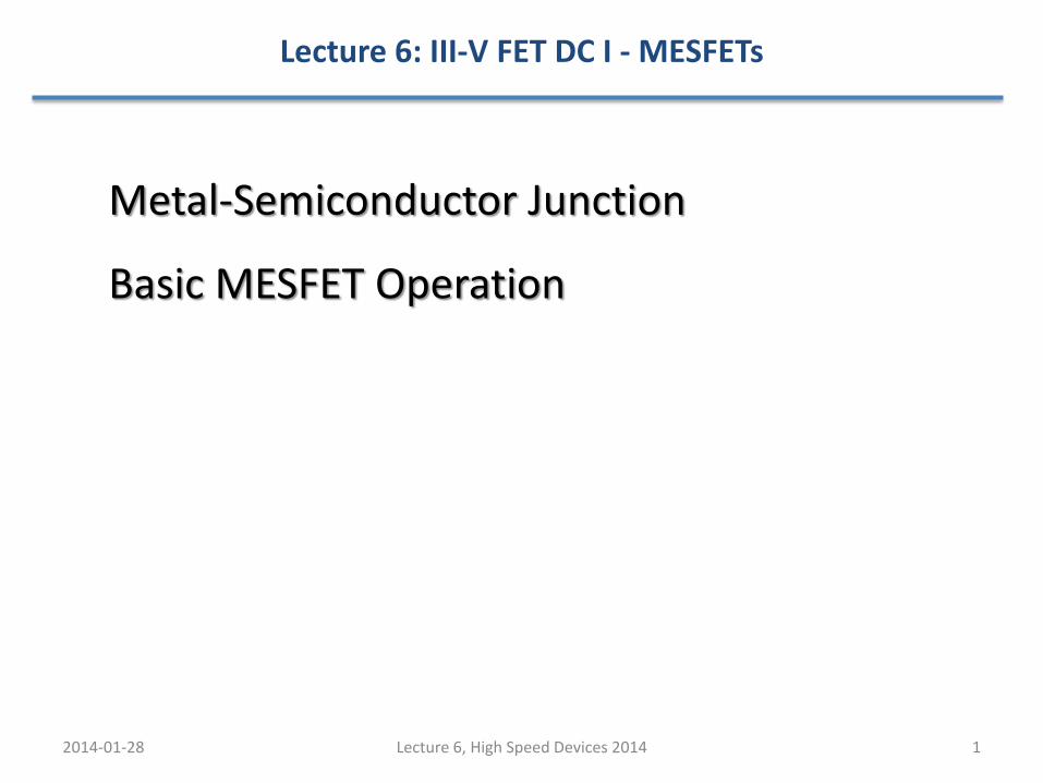
Field Effect Transistors
2014-01-28 2 Lecture 6, High Speed Devices 2014
N+ N+
Source Drain
• The gate electrode controls the carrier concentration in the channel • Source/Drain set the potential at the source/drain side • Electrons flow from source to drain IDS and n(x,y) depend on geometry
and transport properties. • 2D problem (in x and y)
W
Lg
VDS
Vg
x
y
Gate
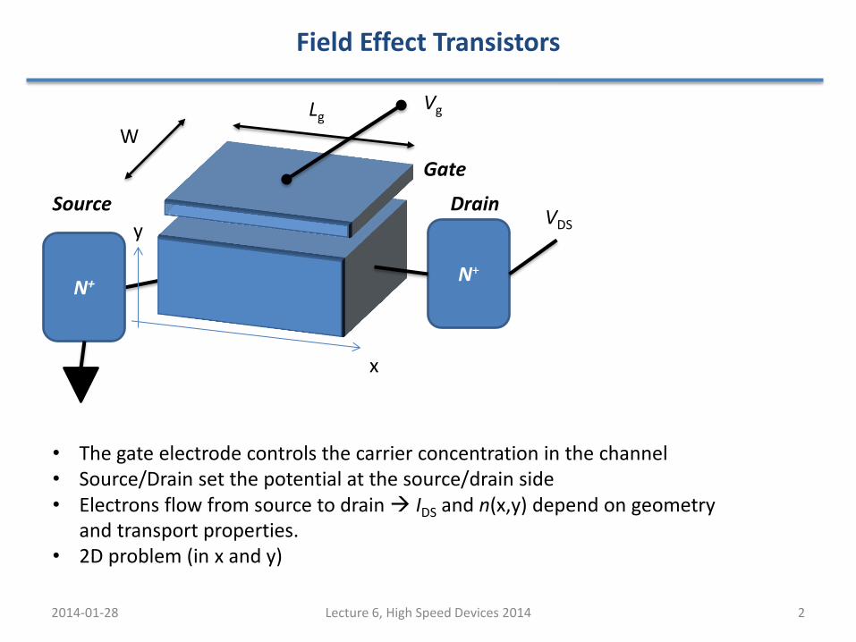
Field Effect Transistors
2014-01-28 3 Lecture 6, High Speed Devices 2014
p-type
n+ n+
Bulk MOSFET
n n+ n+
p-type, S.I. Insulating
MESFET
Metal
Oxide
n- n+ n+
p-type, S.I. Insulating
SOI, Quantum Well MOSFET Metal
Oxide
Oxide or wide bandgap Semicondudctor
Metal Depletion region
Vg=1V
VD=1V
Vg=-1V
n- n+ n+
p-type, S.I. Insulating
HEMT Metal
Wide band semiconductor
Wide band semiconductor
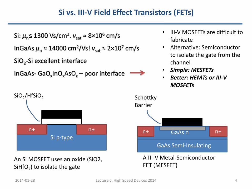
Si vs. III-V Field Effect Transistors (FETs)
2014-01-28 4 Lecture 6, High Speed Devices 2014
Si: µn≤ 1300 Vs/cm2. vsat ≈ 8×106 cm/s
InGaAs µn ≈ 14000 cm2/Vs! vsat ≈ 2×107 cm/s
SiO2-Si excellent interface
InGaAs- GaOxInOxAsOx – poor interface
Si p-type
n+ n+
SiO2/HfSiO2
An Si MOSFET uses an oxide (SiO2, SiHfO2) to isolate the gate
n+ n+
Schottky Barrier
GaAs n
GaAs Semi-Insulating
A III-V Metal-Semiconductor FET (MESFET)
• III-V MOSFETs are difficult to fabricate
• Alternative: Semiconductor to isolate the gate from the channel
• Simple: MESFETs • Better: HEMTs or III-V
MOSFETs

Metal-Semiconductor Junction
2014-01-28 5 Lecture 6, High Speed Devices 2014
qfm
qcs
qfn Fb fbi
q
qqq
nbbi
smb
F
ff
cffSchottky barrier height Build in potential
However, now we ignored that we terminated the crystal and created a lot of surface states....
Too simplistic!
Fb
Similar to a p+N junction!
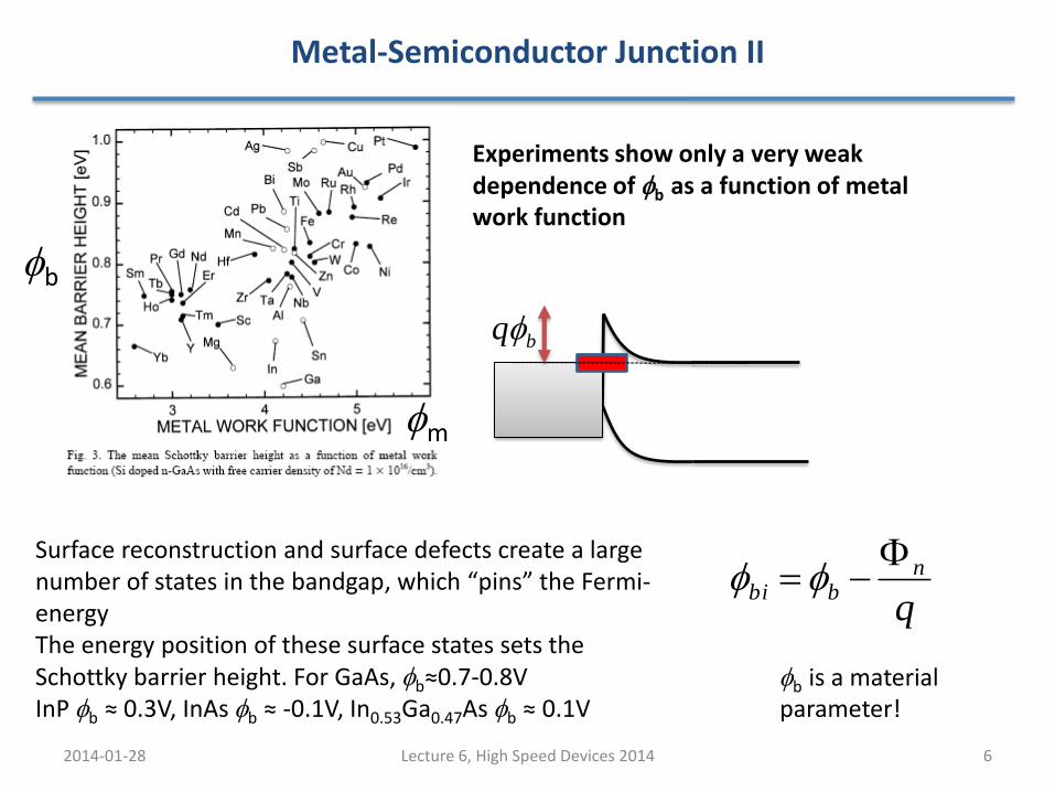
Metal-Semiconductor Junction II
2014-01-28 6 Lecture 6, High Speed Devices 2014
q
nbbi
F ff
Experiments show only a very weak dependence of fb as a function of metal work function
Surface reconstruction and surface defects create a large number of states in the bandgap, which “pins” the Fermi-energy The energy position of these surface states sets the Schottky barrier height. For GaAs, fb≈0.7-0.8V InP fb ≈ 0.3V, InAs fb ≈ -0.1V, In0.53Ga0.47As fb ≈ 0.1V
bqf
fb is a material parameter!
fm
fb
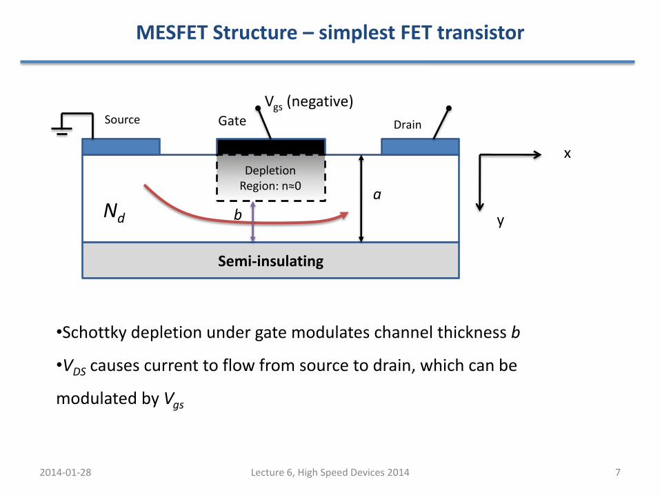
MESFET Structure – simplest FET transistor
2014-01-28 7 Lecture 6, High Speed Devices 2014
Semi-insulating
Vgs (negative) Source Gate Drain
x
y
a Nd
•Schottky depletion under gate modulates channel thickness b
•VDS causes current to flow from source to drain, which can be
modulated by Vgs
b
Depletion Region: n≈0
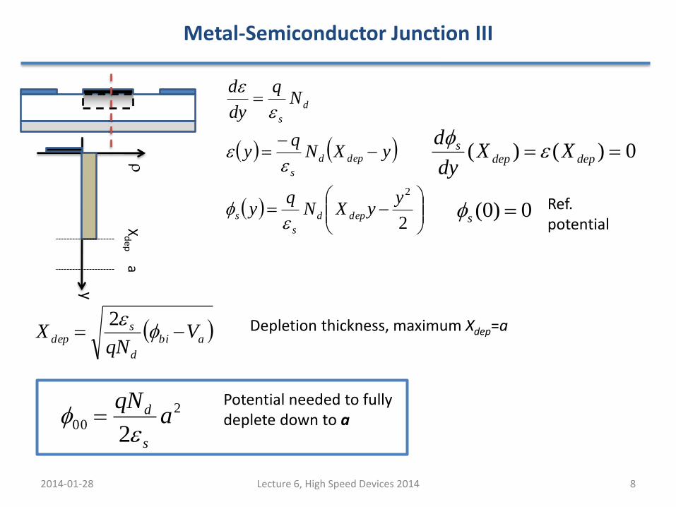
Metal-Semiconductor Junction III
2014-01-28 8 Lecture 6, High Speed Devices 2014
Depletion thickness, maximum Xdep=a
2
2yyXN
qy
yXNq
y
Nq
dy
d
depd
s
s
depd
s
d
s
f
0)0( sf
abi
d
sdep V
qNX f
2
2
002
aqN
s
d
f
Potential needed to fully deplete down to a
y
Xd
ep
a
r
0)()( depdeps XX
dy
d
f
Ref. potential
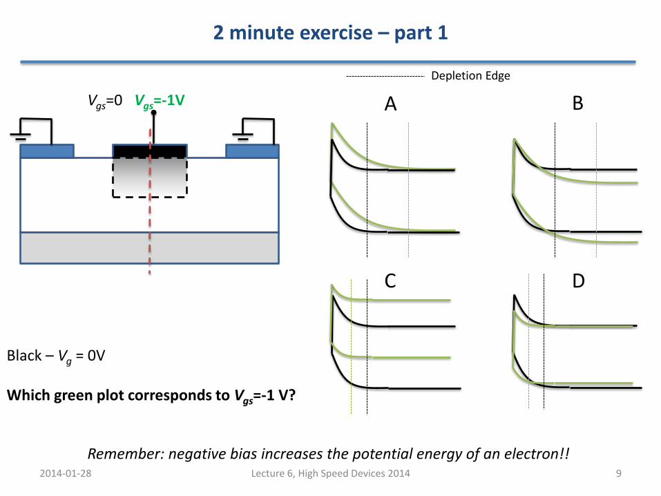
2 minute exercise – part 1
2014-01-28 9 Lecture 6, High Speed Devices 2014
Vgs=0 Vgs=-1V A B
C D
Black – Vg = 0V Which green plot corresponds to Vgs=-1 V?
Remember: negative bias increases the potential energy of an electron!!
Depletion Edge
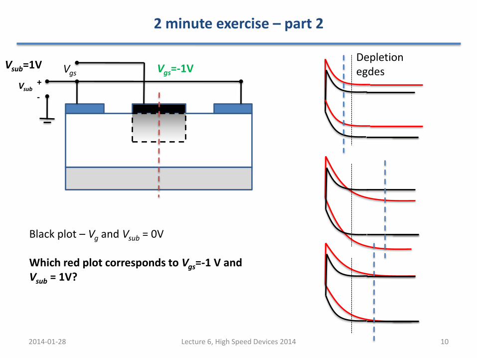
2 minute exercise – part 2
2014-01-28 10 Lecture 6, High Speed Devices 2014
-
+ Vsub
Vgs Vgs=-1V Vsub=1V
Black plot – Vg and Vsub = 0V Which red plot corresponds to Vgs=-1 V and Vsub = 1V?
Depletion egdes
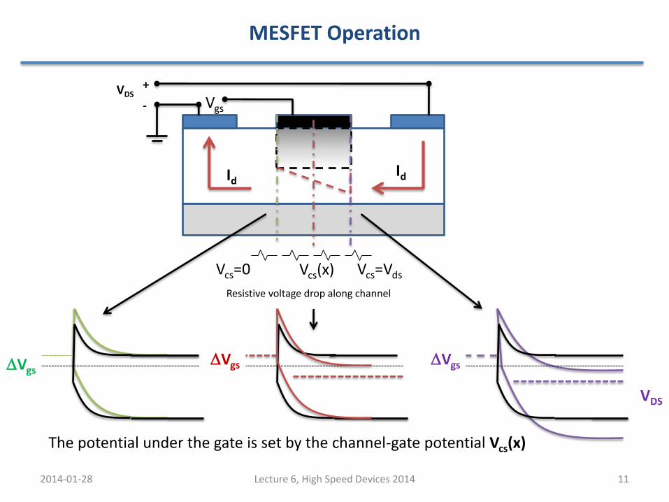
MESFET Operation
2014-01-28 11 Lecture 6, High Speed Devices 2014
DVgs
-
+ VDS Vgs
DVgs
VDS
DVgs
The potential under the gate is set by the channel-gate potential Vcs(x)
Id
Vcs=Vds Vcs=0
Id
Resistive voltage drop along channel
Vcs(x)
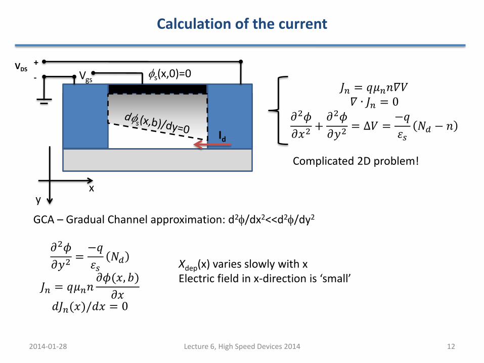
Calculation of the current
2014-01-28 12 Lecture 6, High Speed Devices 2014
-
+ VDS Vgs
Id
𝐽𝑛 = 𝑞𝜇𝑛𝑛𝛻𝑉 𝛻 ∙ 𝐽𝑛 = 0
𝜕2𝜙
𝜕𝑥2+𝜕2𝜙
𝜕𝑦2= ∆𝑉 =
−𝑞
𝜀𝑠𝑁𝑑 − 𝑛
y x
Complicated 2D problem!
GCA – Gradual Channel approximation: d2f/dx2<<d2f/dy2
fs(x,0)=0
𝜕2𝜙
𝜕𝑦2=−𝑞
𝜀𝑠𝑁𝑑
𝐽𝑛 = 𝑞𝜇𝑛𝑛𝜕𝜙(𝑥, 𝑏)
𝜕𝑥
𝑑𝐽𝑛(𝑥)/𝑑𝑥 = 0
Xdep(x) varies slowly with x Electric field in x-direction is ‘small’
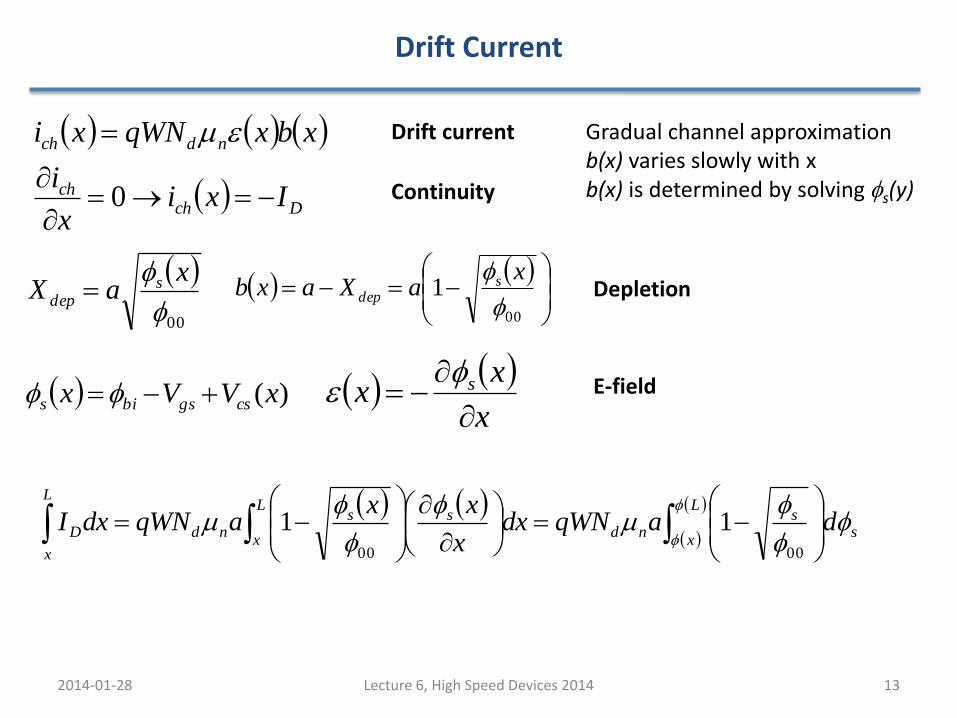
Drift Current
2014-01-28 13 Lecture 6, High Speed Devices 2014
Dchch
ndch
Ixix
i
xbxqWNxi
0
x
xx s
f
00f
f xaX s
dep
00
1f
f xaXaxb s
dep
)(xVVx csgsbis ff
Gradual channel approximation b(x) varies slowly with x b(x) is determined by solving fs(y)
Drift current
Continuity
Depletion
E-field
L
xs
snd
L
x
L
x
ssndD daqWNdx
x
xxaqWNdxI
f
ff
f
f
f
f
f
0000
11
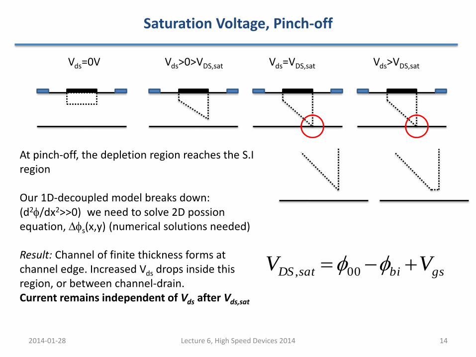
Saturation Voltage, Pinch-off
2014-01-28 14 Lecture 6, High Speed Devices 2014
Vds=0V Vds>0>VDS,sat Vds=VDS,sat Vds>VDS,sat
At pinch-off, the depletion region reaches the S.I region Our 1D-decoupled model breaks down: (d2f/dx2>>0) we need to solve 2D possion equation, Dfs(x,y) (numerical solutions needed) Result: Channel of finite thickness forms at channel edge. Increased Vds drops inside this region, or between channel-drain. Current remains independent of Vds after Vds,sat
gsbisatDS VV ff00,
0 0.5 1 1.5 2 2.5 30
0.02
0.04
0.06
0.08
0.1
0.12
0.14
0.16
Vds
Ids -
arb
units
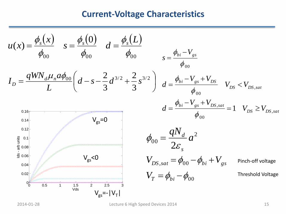
Current-Voltage Characteristics
2014-01-28 15 Lecture 6 High Speed Devices 2014
000000
0)(
f
f
f
f
f
f Lds
xxu sss
2/32/300
3
2
3
2sdsd
L
aqWNI nd
D
f00f
f gsbi Vs
satDSDS
satDSgsbi
satDSDS
DSgsbi
VVVV
d
VVVV
d
,
00
,
,
00
1
f
f
f
f
2
002
aqN
s
d
f
00
00,
ff
ff
biT
gsbisatDS
V
VV Pinch-off voltage Threshold Voltage
Vgs=0
Vgs<0
Vgs=-|VT|

MESFET limitations
2014-01-28 16 Lecture 6, High Speed Devices 2014
2/300
,3
2
3
1ss
L
aqWNI nd
satD
f
00
,1
f
f gsbind
gs
satD
m
V
L
aqWN
dV
dIg
• We want a high gm – but:
• Positive gate-voltage – very high gate leakage!
• From electrostatics: a<L/3 • Increase ND – but this lowers µn due to impurity scattering and increases
gate leakage! • Increase µn by material choice: Need to have a high Schottky barrier!
(InGaAs, InAs can’t be used!)
• We can do better using heterostructures or MOSFETs!