Embed Size (px)
Citation preview

Relion® 650 series
Transformer protectionRET650Technical Manual


Document ID: 1MRK 504 106-UENIssued: September 2009
Revision: -Product version: 1.0
© Copyright 2009 ABB. All rights reserved

CopyrightThis document and parts thereof must not be reproduced or copied without writtenpermission from ABB, and the contents thereof must not be imparted to a thirdparty, nor used for any unauthorized purpose.
The software or hardware described in this document is furnished under a licenseand may be used or disclosed only in accordance with the terms of such license.
TrademarksABB and Relion are registered trademarks of ABB Group. All other brand orproduct names mentioned in this document may be trademarks or registeredtrademarks of their respective holders.
WarrantyPlease inquire about the terms of warranty from your nearest ABB representative.
ABB AB
Substation Automation Products
SE-721 59 Västerås
Sweden
Telephone: +46 (0) 21 34 20 00
Facsimile: +46 (0) 21 14 69 18
http://www.abb.com/substationautomation

DisclaimerThe data, examples and diagrams in this manual are included solely for the conceptor product description and are not to be deemed as a statement of guaranteedproperties. All persons responsible for applying the equipment addressed in thismanual must satisfy themselves that each intended application is suitable andacceptable, including that any applicable safety or other operational requirementsare complied with. In particular, any risks in applications where a system failure and/or product failure would create a risk for harm to property or persons (including butnot limited to personal injuries or death) shall be the sole responsibility of theperson or entity applying the equipment, and those so responsible are herebyrequested to ensure that all measures are taken to exclude or mitigate such risks.
This document has been carefully checked by ABB but deviations cannot becompletely ruled out. In case any errors are detected, the reader is kindly requestedto notify the manufacturer. Other than under explicit contractual commitments, inno event shall ABB be responsible or liable for any loss or damage resulting fromthe use of this manual or the application of the equipment.

ConformityThis product complies with the directive of the Council of the EuropeanCommunities on the approximation of the laws of the Member States relating toelectromagnetic compatibility (EMC Directive 2004/108/EC) and concerningelectrical equipment for use within specified voltage limits (Low-voltage directive2006/95/EC).
This conformity is proved by tests conducted by ABB AB in accordance with thegeneric standard EN 50263 for the EMC directive, and with the standards EN60255-5 and/or EN 50178 for the low voltage directive.
This product is designed and produced for industrial use.

Table of contents
Section 1 Introduction.....................................................................23This manual......................................................................................23Intended audience............................................................................23Product documentation.....................................................................24
Product documentation set..........................................................24Document revision history...........................................................25Related documents......................................................................25
Symbols and conventions.................................................................26Safety indication symbols............................................................26Manual conventions.....................................................................27
Section 2 Available functions.........................................................29Main protection functions..................................................................29Back-up protection functions............................................................29Control and monitoring functions......................................................30Designed to communicate................................................................32Basic IED functions..........................................................................32
Section 3 Local Human-Machine-Interface LHMI...........................33Local HMI screen behaviour.............................................................33
Identification................................................................................33Settings........................................................................................33
Local HMI signals.............................................................................33Identification................................................................................33Function block.............................................................................34Signals.........................................................................................34
Basic part for LED indication module...............................................34Identification................................................................................34Function block.............................................................................35Signals.........................................................................................35Settings........................................................................................36
LCD part for HMI function keys control module................................36Identification................................................................................36Function block.............................................................................36Signals.........................................................................................37Settings........................................................................................37
Operation principle...........................................................................38Local HMI....................................................................................38
LCD........................................................................................38LEDs.......................................................................................41
Table of contents
RET650 1Technical Manual

Keypad...................................................................................41LED..............................................................................................42
Functionality...........................................................................42Status LEDs...........................................................................43Indication LEDs......................................................................43
Function keys..............................................................................51Functionality...........................................................................51Operation principle.................................................................51
Section 4 Differential protection.....................................................53Transformer differential protection....................................................53
Functionality................................................................................53Transformer differential protection, two-winding T2WPDIF.........54
Identification...........................................................................54Signals....................................................................................54Settings..................................................................................55Monitored data.......................................................................56
Transformer differential protection, three-windingT3WPDIF ....................................................................................57
Identification...........................................................................57Signals....................................................................................57Settings..................................................................................58Monitored data.......................................................................60
Operation principle......................................................................60Differential current alarm........................................................61Bias current............................................................................61Elimination of zero sequence currents...................................62Restrained, and unrestrained limits of the differentialprotection................................................................................62Fundamental frequency negative sequence differentialcurrents..................................................................................65Internal/external fault discriminator........................................65Unrestrained, and sensitive negative sequenceprotections..............................................................................69Harmonic and waveform block criteria...................................70Switch onto fault feature.........................................................72Logic diagram.........................................................................72
Technical data.............................................................................74Restricted earth-fault protection, low impedance REFPDIF.............74
Identification................................................................................74Functionality................................................................................75Function block.............................................................................75Signals.........................................................................................75Settings........................................................................................76
Table of contents
2 RET650Technical Manual

Monitored data.............................................................................76Operation principle......................................................................77
Fundamental principles of the restricted earth-faultprotection................................................................................77Restricted earth-fault protection, low impedance as adifferential protection..............................................................80Calculation of differential current and bias current.................81Detection of external earth-faults...........................................81
Technical data.............................................................................83
Section 5 Current protection...........................................................85Instantaneous phase overcurrent protection PHPIOC.....................85
Identification ...............................................................................85Functionality................................................................................85Function block.............................................................................85Signals.........................................................................................85Settings........................................................................................86Monitored data.............................................................................86Operation principle......................................................................86Technical data.............................................................................86
Four step phase overcurrent protection OC4PTOC.........................87Identification ...............................................................................87Functionality................................................................................87Function block.............................................................................87Signals.........................................................................................88Settings........................................................................................89Monitored data.............................................................................90Operation principle......................................................................91Technical data.............................................................................94
Instantaneous residual overcurrent protection EFPIOC...................94Identification ...............................................................................94Functionality................................................................................94Function block.............................................................................95Signals.........................................................................................95Settings........................................................................................95Monitored data.............................................................................95Operation principle......................................................................96Technical data.............................................................................96
Four step residual overcurrent protection EF4PTOC.......................96Identification ...............................................................................96Functionality................................................................................96Function block.............................................................................97Signals.........................................................................................97Settings........................................................................................98
Table of contents
RET650 3Technical Manual

Monitored data...........................................................................101Operation principle....................................................................101
Operating quantity within the function..................................101Internal polarizing.................................................................102External polarizing for earth-fault function............................104Base quantities within the protection....................................104Internal earth-fault protection structure................................104Four residual overcurrent steps............................................105Directional supervision element with integrateddirectional comparison function............................................106
Technical data...........................................................................108Thermal overload protection, two time constants TRPTTR............109
Identification .............................................................................109Functionality..............................................................................109Function block...........................................................................110Signals.......................................................................................110Settings......................................................................................111Monitored data...........................................................................112Operation principle....................................................................112Technical data...........................................................................116
Breaker failure protection CCRBRF...............................................116Identification..............................................................................116Functionality..............................................................................116Function block...........................................................................117Signals.......................................................................................117Settings......................................................................................117Monitored data...........................................................................118Operation principle....................................................................118Technical data...........................................................................120
Pole discordance protection CCRPLD...........................................120Identification .............................................................................120Functionality..............................................................................120Function block...........................................................................121Signals.......................................................................................121Settings......................................................................................121Monitored data...........................................................................122Operation principle....................................................................122
Pole discordance signalling from circuit breaker..................123Unsymmetrical current detection..........................................124
Technical data...........................................................................124Directional over-/under-power protection GOPPDOP/GUPPDUP......................................................................................124
Functionality..............................................................................124Directional over-power protection GOPPDOP...........................125
Table of contents
4 RET650Technical Manual

Identification.........................................................................125Function block......................................................................125Signals..................................................................................125Settings................................................................................126Monitored data.....................................................................127
Directional under-power protection GUPPDUP.........................127Identification.........................................................................127Function block......................................................................128Signals..................................................................................128Settings................................................................................129Monitored data.....................................................................130
Operation principle....................................................................130Low pass filtering..................................................................132
Technical data...........................................................................132Negative sequence based overcurrent function DNSPTOC...........133
Identification..............................................................................133Functionality..............................................................................133Function block...........................................................................133Signals.......................................................................................134Settings......................................................................................134Monitored data...........................................................................135Operation principle....................................................................136Technical data...........................................................................136
Section 6 Voltage protection........................................................137Two step undervoltage protection UV2PTUV.................................137
Identification..............................................................................137Functionality..............................................................................137Function block...........................................................................137Signals.......................................................................................138Settings......................................................................................138Monitored data...........................................................................139Operation principle....................................................................139
Measurement principle.........................................................140Time delay............................................................................140Blocking................................................................................143Design..................................................................................144
Technical data...........................................................................145Two step overvoltage protection OV2PTOV...................................145
Identification..............................................................................145Functionality..............................................................................145Function block...........................................................................146Signals.......................................................................................146Settings......................................................................................147
Table of contents
RET650 5Technical Manual

Monitored data...........................................................................147Operation principle....................................................................148
Measurement principle.........................................................148Time delay............................................................................148Blocking................................................................................150Design..................................................................................151
Technical data...........................................................................152Two step residual overvoltage protection ROV2PTOV..................152
Identification..............................................................................152Functionality..............................................................................152Function block...........................................................................153Signals.......................................................................................153Settings......................................................................................154Monitored data...........................................................................154Operation principle....................................................................154
Measurement principle.........................................................155Time delay............................................................................155Blocking................................................................................158Design..................................................................................159
Technical data...........................................................................160Overexcitation protection OEXPVPH.............................................160
Identification..............................................................................160Functionality..............................................................................160Function block...........................................................................161Signals.......................................................................................161Settings......................................................................................161Monitored data...........................................................................162Operation principle....................................................................162
Measured voltage.................................................................164Operate time of the overexcitation protection.......................164Cooling.................................................................................167Overexcitation protection function measurands...................167Overexcitation alarm............................................................168Logic diagram.......................................................................168
Technical data...........................................................................168
Section 7 Frequency protection....................................................171Under frequency protection SAPTUF.............................................171
Identification..............................................................................171Functionality..............................................................................171Function block...........................................................................171Signals.......................................................................................171Settings......................................................................................172Monitored data...........................................................................172
Table of contents
6 RET650Technical Manual

Operation principle....................................................................172Measurement principle.........................................................172Time delay............................................................................173Blocking................................................................................173Design..................................................................................173
Technical data...........................................................................174Over frequency protection SAPTOF...............................................174
Identification..............................................................................174Functionality..............................................................................175Function block...........................................................................175Signals.......................................................................................175Settings......................................................................................176Monitored data...........................................................................176Operation principle....................................................................176
Measurement principle.........................................................176Time delay............................................................................176Blocking................................................................................177Design..................................................................................177
Technical data...........................................................................178Rate-of-change frequency protection SAPFRC..............................178
Identification..............................................................................178Functionality..............................................................................178Function block...........................................................................178Signals.......................................................................................179Settings......................................................................................179Operation principle....................................................................179
Measurement principle.........................................................180Time delay............................................................................180Design..................................................................................181
Technical data...........................................................................181
Section 8 Secondary system supervision.....................................183Breaker close/trip circuit monitoring TCSSCBR.............................183
Identification..............................................................................183Functionality..............................................................................183Function block...........................................................................183Signals.......................................................................................183Settings......................................................................................184Monitored data...........................................................................184Operation principle....................................................................184Technical data...........................................................................185
Section 9 Control..........................................................................187Apparatus control APC...................................................................187
Table of contents
RET650 7Technical Manual

Functionality..............................................................................187Bay control QCBAY...................................................................187
Identification ........................................................................187Functionality.........................................................................187Function block......................................................................187Signals..................................................................................188Settings................................................................................188
Local remote LOCREM.............................................................188Identification ........................................................................188Functionality.........................................................................188Function block......................................................................189Signals..................................................................................189Settings................................................................................189
Local remote control LOCREMCTRL........................................189Identification ........................................................................189Functionality.........................................................................190Function block......................................................................190Signals..................................................................................190Settings................................................................................191
Operation principle....................................................................191Bay control QCBAY .............................................................191Local remote/Local remote control LOCREM/LOCREMCTRL.....................................................................193
Voltage control ...............................................................................193Functionality..............................................................................193Automatic voltage control for tap changer, single control(TR1ATCC)................................................................................194
Identification.........................................................................194Function block......................................................................195Signals..................................................................................195Settings................................................................................196Monitored data.....................................................................199
Automatic voltage control for tap changer, parallel control(TR8ATCC)................................................................................199
Identification.........................................................................199Function block......................................................................200Signals..................................................................................200Settings................................................................................202Monitored data.....................................................................206
Tap changer control and supervision, 6 binary inputs(TCMYLTC)...............................................................................206
Identification.........................................................................206Function block......................................................................207Signals..................................................................................207
Table of contents
8 RET650Technical Manual

Settings................................................................................208Monitored data.....................................................................209
Operation principle....................................................................209Automatic voltage control for tap changer (TR1ATCC forsingle control and TR8ATCC parallel control)......................210Tap changer control and supervision, 6 binary inputs(TCMYLTC)..........................................................................214Connection between TR1ATCC or TR8ATCC andTCMYLTC............................................................................216
Technical data...........................................................................219Logic rotating switch for function selection and LHMIpresentation SLGGIO.....................................................................221
Identification..............................................................................221Functionality..............................................................................221Function block...........................................................................221Signals.......................................................................................222Settings......................................................................................223Monitored data...........................................................................223Operation principle....................................................................223
Selector mini switch VSGGIO.........................................................224Identification..............................................................................224Functionality..............................................................................224Function block...........................................................................224Signals.......................................................................................225Settings......................................................................................225Operation principle....................................................................225
IEC 61850 generic communication I/O functions DPGGIO............226Identification..............................................................................226Functionality..............................................................................226Function block...........................................................................227Signals.......................................................................................227Settings......................................................................................227Operation principle....................................................................227
Single point generic control 8 signals SPC8GGIO.........................227Identification..............................................................................227Functionality..............................................................................228Function block...........................................................................228Signals.......................................................................................228Settings......................................................................................229Operation principle....................................................................229
Automation bits AUTOBITS............................................................230Identification..............................................................................230Functionality..............................................................................230Function block...........................................................................230
Table of contents
RET650 9Technical Manual

Signals.......................................................................................231Settings......................................................................................232Operation principle....................................................................232
Section 10 Logic.............................................................................233Tripping logic SMPPTRC................................................................233
Identification..............................................................................233Functionality..............................................................................233Function block...........................................................................233Signals.......................................................................................234Settings......................................................................................234Operation principle....................................................................234Technical data...........................................................................235
Trip matrix logic TMAGGIO............................................................235Identification..............................................................................235Functionality..............................................................................235Function block...........................................................................236Signals.......................................................................................236Settings......................................................................................237Operation principle....................................................................238
Configurable logic blocks................................................................239Standard configurable logic blocks............................................239
Functionality.........................................................................239OR function block.................................................................240Inverter function block INVERTER.......................................241PULSETIMER function block ..............................................242Controllable gate function block GATE................................243Exclusive OR function block XOR........................................243Loop delay function block LOOPDELAY..............................244Timer function block TIMERSET..........................................245AND function block ..............................................................246Set-reset memory function block SRMEMORY....................247Reset-set with memory function block RSMEMORY...........248
Technical data...........................................................................250Fixed signals FXDSIGN..................................................................250
Identification..............................................................................250Functionality..............................................................................250Function block...........................................................................250Signals.......................................................................................251Settings......................................................................................251Operation principle....................................................................251
Boolean 16 to integer conversion B16I...........................................251Identification..............................................................................251Functionality..............................................................................252
Table of contents
10 RET650Technical Manual

Function block...........................................................................252Signals.......................................................................................252Settings......................................................................................253Monitored data...........................................................................253Operation principle....................................................................253
Boolean 16 to integer conversion with logic noderepresentation B16IFCVI................................................................253
Identification..............................................................................253Functionality..............................................................................253Function block...........................................................................254Signals.......................................................................................254Settings......................................................................................255Monitored data...........................................................................255Operation principle....................................................................255
Integer to boolean 16 conversion IB16A........................................255Identification..............................................................................255Functionality..............................................................................255Function block...........................................................................256Signals.......................................................................................256Settings......................................................................................257Operation principle....................................................................257
Integer to boolean 16 conversion with logic noderepresentation IB16FCVB...............................................................257
Identification..............................................................................257Functionality..............................................................................257Function block...........................................................................258Signals.......................................................................................258Settings......................................................................................259Operation principle....................................................................259
Section 11 Monitoring.....................................................................261IEC 61850 generic communication I/O functions SPGGIO............261
Identification..............................................................................261Functionality..............................................................................261Function block...........................................................................261Signals.......................................................................................261Settings......................................................................................261Operation principle....................................................................262
IEC 61850 generic communication I/O functions 16 inputsSP16GGIO.....................................................................................262
Identification..............................................................................262Functionality..............................................................................262Function block...........................................................................262Signals.......................................................................................263
Table of contents
RET650 11Technical Manual

Settings......................................................................................263Operation principle....................................................................263
IEC 61850 generic communication I/O functions MVGGIO............264Identification..............................................................................264Functionality..............................................................................264Function block...........................................................................264Signals.......................................................................................264Settings......................................................................................265Monitored data...........................................................................265Operation principle....................................................................265
Measurements................................................................................266Functionality..............................................................................266Measurements CVMMXN..........................................................267
Identification ........................................................................267Function block......................................................................267Signals..................................................................................268Settings................................................................................269Monitored data.....................................................................272
Phase current measurement CMMXU.......................................272Identification ........................................................................272Function block......................................................................272Signals..................................................................................273Settings................................................................................273Monitored data.....................................................................274
Phase-phase voltage measurement VMMXU...........................274Identification ........................................................................274Function block......................................................................275Signals..................................................................................275Settings................................................................................275Monitored data.....................................................................276
Current sequence component measurement CMSQI...............276Identification ........................................................................276Function block......................................................................277Signals..................................................................................277Settings................................................................................277Monitored data.....................................................................279
Voltage sequence measurement VMSQI..................................279Identification ........................................................................279Function block......................................................................279Signals..................................................................................280Settings................................................................................280Monitored data.....................................................................281
Phase-neutral voltage measurement VNMMXU........................282
Table of contents
12 RET650Technical Manual

Identification ........................................................................282Function block......................................................................282Signals..................................................................................282Settings................................................................................283Monitored data.....................................................................284
Operation principle....................................................................284Measurement supervision....................................................284Measurements CVMMXN.....................................................288Phase current measurement CMMXU.................................293Phase-phase and phase-neutral voltage measurementsVMMXU/VNMMXU...............................................................294Voltage and current sequence measurements VMSQI/CMSQI..................................................................................294
Technical data...........................................................................294Event Counter CNTGGIO...............................................................295
Identification..............................................................................295Functionality..............................................................................295Function block...........................................................................295Signals.......................................................................................295Settings......................................................................................296Monitored data...........................................................................296Operation principle....................................................................296
Reporting..............................................................................297Technical data...........................................................................297
Disturbance report..........................................................................297Functionality..............................................................................297Disturbance report DRPRDRE..................................................298
Identification.........................................................................298Function block......................................................................298Signals..................................................................................298Settings................................................................................299Monitored data.....................................................................299Measured values..................................................................303
Analog input signals AxRADR...................................................303Identification.........................................................................303Function block......................................................................304Signals..................................................................................304Settings................................................................................305
Analog input signals A4RADR...................................................307Identification.........................................................................307Function block......................................................................308Signals..................................................................................308Settings................................................................................308
Binary input signals BxRBDR....................................................311
Table of contents
RET650 13Technical Manual

Identification.........................................................................311Function block......................................................................311Signals..................................................................................312Settings................................................................................312
Operation principle....................................................................316Disturbance information.......................................................318Indications ...........................................................................318Event recorder .....................................................................318Event list ..............................................................................318Trip value recorder ..............................................................318Disturbance recorder ...........................................................318Time tagging.........................................................................318Recording times...................................................................319Analog signals......................................................................319Binary signals.......................................................................321Trigger signals......................................................................321Post Retrigger......................................................................322
Technical data...........................................................................323Indications......................................................................................323
Functionality..............................................................................323Function block...........................................................................324Signals.......................................................................................324
Input signals.........................................................................324Operation principle....................................................................324Technical data...........................................................................325
Event recorder ...............................................................................325Functionality..............................................................................325Function block...........................................................................325Signals.......................................................................................326
Input signals.........................................................................326Operation principle....................................................................326Technical data...........................................................................326
Event list.........................................................................................326Functionality..............................................................................326Function block...........................................................................327Signals.......................................................................................327
Input signals.........................................................................327Operation principle....................................................................327Technical data...........................................................................328
Trip value recorder.........................................................................328Functionality..............................................................................328Function block...........................................................................328Signals.......................................................................................328
Table of contents
14 RET650Technical Manual

Input signals.........................................................................328Operation principle....................................................................328Technical data...........................................................................329
Disturbance recorder......................................................................329Functionality..............................................................................329Function block...........................................................................330Signals.......................................................................................330
Input and output signals.......................................................330Setting parameters....................................................................330Operation principle....................................................................330
Memory and storage............................................................331Technical data...........................................................................332
Measured value expander block MVEXP.......................................332Identification..............................................................................332Functionality..............................................................................332Function block...........................................................................333Signals.......................................................................................333Settings......................................................................................333Operation principle....................................................................333
Station battery supervision SPVNZBAT.........................................334Identification..............................................................................334Functionality..............................................................................334Function block...........................................................................334Signals.......................................................................................335Settings......................................................................................335Monitored data...........................................................................335Operation principle ...................................................................335
Insulation gas monitoring function SSIMG.....................................337Identification..............................................................................337Functionality..............................................................................337Function block...........................................................................337Signals.......................................................................................338Settings......................................................................................338Operation principle....................................................................339Technical data...........................................................................339
Insulation liquid monitoring function SSIML....................................340Identification..............................................................................340Functionality..............................................................................340Function block...........................................................................340Signals.......................................................................................340Settings......................................................................................341Operation principle....................................................................341Technical data...........................................................................342
Table of contents
RET650 15Technical Manual

Circuit breaker condition monitoring SSCBR..................................342Identification..............................................................................342Functionality..............................................................................342Function block...........................................................................343Signals.......................................................................................343Settings......................................................................................344Monitored data...........................................................................345Operation principle....................................................................345
Circuit breaker status...........................................................346Circuit breaker operation monitoring....................................347Breaker contact travel time...................................................348Operation counter.................................................................349Accumulation of Iyt................................................................350Remaining life of the circuit breaker.....................................352Circuit breaker spring charged indication.............................353Gas pressure supervision.....................................................354
Technical data...........................................................................355
Section 12 Metering.......................................................................357Pulse counter PCGGIO..................................................................357
Identification..............................................................................357Functionality..............................................................................357Function block...........................................................................357Signals.......................................................................................357Settings......................................................................................358Monitored data...........................................................................358Operation principle....................................................................358Technical data...........................................................................360
Energy calculation and demand handling ETPMMTR....................360Identification..............................................................................360Functionality..............................................................................360Function block...........................................................................361Signals.......................................................................................361Settings......................................................................................362Monitored data...........................................................................363Operation principle....................................................................363Technical data...........................................................................364
Section 13 Station communication.................................................365DNP3 protocol................................................................................365IEC 61850-8-1 communication protocol ........................................365
Identification..............................................................................365Functionality..............................................................................365Settings......................................................................................366
Table of contents
16 RET650Technical Manual

Technical data...........................................................................366Horizontal communication via GOOSE for interlocking..................366
Identification..............................................................................366Function block...........................................................................367Signals.......................................................................................367Settings......................................................................................369
Goose binary receive GOOSEBINRCV..........................................369Identification..............................................................................369Function block...........................................................................370Signals.......................................................................................370Settings......................................................................................371
Section 14 Basic IED functions......................................................373Self supervision with internal event list ..........................................373
Functionality..............................................................................373Internal error signals INTERRSIG.............................................373
Identification.........................................................................373Function block......................................................................373Signals..................................................................................373Settings................................................................................374
Internal event list SELFSUPEVLST...........................................374Identification.........................................................................374Settings................................................................................374
Operation principle....................................................................374Internal signals.....................................................................376Run-time model....................................................................378
Technical data...........................................................................379Time synchronization......................................................................379
Functionality..............................................................................379Time synchronization TIMESYNCHGEN...................................380
Identification.........................................................................380Settings................................................................................380
Time synchronization via SNTP................................................380Identification.........................................................................380Settings................................................................................380
Time system, summer time begin DTSBEGIN..........................380Identification.........................................................................380Settings................................................................................381
Time system, summer time ends DTSEND...............................381Identification.........................................................................381Settings................................................................................382
Time zone from UTC TIMEZONE..............................................382Identification.........................................................................382Settings................................................................................382
Table of contents
RET650 17Technical Manual

Time synchronization via IRIG-B...............................................383Identification.........................................................................383Settings................................................................................383
Operation principle....................................................................383General concepts.................................................................383Real-time clock (RTC) operation..........................................385Synchronization alternatives................................................386
Technical data...........................................................................387Parameter setting group handling..................................................387
Functionality..............................................................................387Setting group handling SETGRPS............................................387
Identification.........................................................................387Settings................................................................................387
Parameter setting groups ACTVGRP........................................388Identification.........................................................................388Function block......................................................................388Signals..................................................................................388Settings................................................................................388
Operation principle....................................................................389Test mode functionality TESTMODE..............................................390
Identification..............................................................................390Functionality..............................................................................390Function block...........................................................................390Signals.......................................................................................391Settings......................................................................................391Operation principle....................................................................391
Change lock function CHNGLCK ..................................................392Identification..............................................................................392Functionality..............................................................................393Function block...........................................................................393Signals.......................................................................................393Settings......................................................................................393Operation principle....................................................................394
IED identifiers TERMINALID..........................................................394Identification..............................................................................394Functionality..............................................................................394Settings......................................................................................395
Product information .......................................................................395Identification..............................................................................395Functionality..............................................................................395Settings......................................................................................395
Primary system values PRIMVAL...................................................396Identification..............................................................................396
Table of contents
18 RET650Technical Manual

Functionality..............................................................................396Settings......................................................................................396
Signal matrix for analog inputs SMAI.............................................396Functionality..............................................................................396Signal matrix for analog inputs SMAI_20_1...............................396
Identification.........................................................................396Function block......................................................................397Signals..................................................................................397Settings................................................................................398
Signal matrix for analog inputs SMAI_20_2...............................399Identification.........................................................................399Function block......................................................................399Signals..................................................................................399Settings................................................................................400
Operation principle ...................................................................401Summation block 3 phase 3PHSUM..............................................401
Identification..............................................................................401Functionality..............................................................................401Function block...........................................................................401Signals.......................................................................................402Settings......................................................................................402Operation principle....................................................................403
Global base values GBASVAL.......................................................403Identification..............................................................................403Functionality..............................................................................403Settings......................................................................................403
Authority check ATHCHCK.............................................................404Identification..............................................................................404Functionality..............................................................................404Settings......................................................................................404Operation principle....................................................................404
Authorization handling in the IED.........................................405Authority status ATHSTAT.............................................................406
Identification..............................................................................406Functionality..............................................................................406Function block...........................................................................406Signals.......................................................................................406Settings......................................................................................406Operation principle....................................................................406
Denial of service.............................................................................407Functionality..............................................................................407Denial of service, frame rate control for front portDOSFRNT.................................................................................407
Table of contents
RET650 19Technical Manual

Identification.........................................................................407Function block......................................................................407Signals..................................................................................407Settings................................................................................408Monitored data.....................................................................408
Denial of service, frame rate control for LAN1 portDOSLAN1..................................................................................408
Identification.........................................................................408Function block......................................................................409Signals..................................................................................409Settings................................................................................409Monitored data.....................................................................409
Operation principle....................................................................410
Section 15 IED physical connections.............................................411Protective earth connections..........................................................411Inputs..............................................................................................413
Measuring inputs.......................................................................413Auxiliary supply voltage input....................................................413Binary inputs..............................................................................414
Outputs...........................................................................................417Outputs for tripping, controlling and signalling...........................417Outputs for signalling.................................................................419IRF.............................................................................................421
Communication connections..........................................................421Ethernet RJ-45 front connection................................................421Station communication rear connection....................................422Communication interfaces and protocols..................................422Recommended industrial Ethernet switches.............................422
Connection diagrams......................................................................423
Section 16 Technical data..............................................................449Dimensions.....................................................................................449Power supply..................................................................................449Energizing inputs............................................................................450Binary inputs...................................................................................450Signal outputs.................................................................................451Power outputs.................................................................................451Data communication interfaces......................................................451Enclosure class..............................................................................452Environmental conditions and tests................................................452
Section 17 IED and functionality tests............................................455Electromagnetic compatibility tests................................................455
Table of contents
20 RET650Technical Manual

Insulation tests................................................................................456Mechanical tests.............................................................................457Product safety.................................................................................457EMC compliance............................................................................457
Section 18 Time inverse characteristics.........................................459Application......................................................................................459Operation principle.........................................................................462
Mode of operation......................................................................462Inverse time characteristics............................................................465
Section 19 Glossary.......................................................................489
Table of contents
RET650 21Technical Manual

22

Section 1 Introduction
1.1 This manual
The technical manual contains application and functionality descriptions and listsfunction blocks, logic diagrams, input and output signals, setting parameters andtechnical data sorted per function. The manual can be used as a technical referenceduring the engineering phase, installation and commissioning phase, and duringnormal service.
1.2 Intended audience
This manual addresses system engineers and installation and commissioningpersonnel, who use technical data during engineering, installation andcommissioning, and in normal service.
The system engineer must have a thorough knowledge of protection systems,protection equipment, protection functions and the configured functional logic inthe IEDs. The installation and commissioning personnel must have a basicknowledge in handling electronic equipment.
1MRK 504 106-UEN - Section 1Introduction
RET650 23Technical Manual

1.3 Product documentation
1.3.1 Product documentation set
Pla
nnin
g &
pur
chas
e
Eng
inee
ring
Inst
allin
g
Com
mis
sion
ing
Ope
ratio
n
Mai
nten
ance
Dec
omm
issi
onin
gde
inst
allin
g&
dis
posa
l
Application manual
Operation manual
Installation manual
Service manual
Engineering manual
Commissioning manual
Communication protocolmanual
Technical manual
Pla
nnin
g &
pur
chas
e
Eng
inee
ring
Inst
allin
g
Com
mis
sion
ing
Ope
ratio
n
Mai
nten
ance
Dec
omm
issi
onin
gde
inst
allin
g&
dis
posa
l
Pla
nnin
g &
pur
chas
e
Eng
inee
ring
Inst
allin
g
Com
mis
sion
ing
Ope
ratio
n
Mai
nten
ance
Dec
omm
issi
onin
gde
inst
allin
g&
dis
posa
l
Application manualApplication manual
Operation manualOperation manual
Installation manualInstallation manual
Service manualService manual
Engineering manualEngineering manual
Commissioning manualCommissioning manual
Communication protocolmanualCommunication protocolmanual
Technical manualTechnical manual
en07000220.vsd
IEC07000220 V1 EN
Figure 1: The intended use of manuals in different lifecycles
The engineering manual contains instructions on how to engineer the IEDs usingthe different tools in PCM600. The manual provides instructions on how to set up aPCM600 project and insert IEDs to the project structure. The manual alsorecommends a sequence for engineering of protection and control functions, LHMIfunctions as well as communication engineering for IEC 61850 and DNP3.
The installation manual contains instructions on how to install the IED. Themanual provides procedures for mechanical and electrical installation. The chaptersare organized in chronological order in which the IED should be installed.
The commissioning manual contains instructions on how to commission the IED.The manual can also be used by system engineers and maintenance personnel forassistance during the testing phase. The manual provides procedures for checkingof external circuitry and energizing the IED, parameter setting and configuration aswell as verifying settings by secondary injection. The manual describes the process
Section 1 1MRK 504 106-UEN -Introduction
24 RET650Technical Manual

of testing an IED in a substation which is not in service. The chapters are organizedin chronological order in which the IED should be commissioned.
The operation manual contains instructions on how to operate the IED once it hasbeen commissioned. The manual provides instructions for monitoring, controllingand setting the IED. The manual also describes how to identify disturbances andhow to view calculated and measured power grid data to determine the cause of afault.
The service manual contains instructions on how to service and maintain the IED.The manual also provides procedures for de-energizing, de-commissioning anddisposal of the IED.
The application manual contains application descriptions and setting guidelinessorted per function. The manual can be used to find out when and for what purposea typical protection function can be used. The manual can also be used whencalculating settings.
The technical manual contains application and functionality descriptions and listsfunction blocks, logic diagrams, input and output signals, setting parameters andtechnical data sorted per function. The manual can be used as a technical referenceduring the engineering phase, installation and commissioning phase, and duringnormal service.
The communication protocol manual describes a communication protocolsupported by the IED. The manual concentrates on vendor-specific implementations.
The point list manual describes the outlook and properties of the data pointsspecific to the IED. The manual should be used in conjunction with thecorresponding communication protocol manual.
The service manual is not available yet.
1.3.2 Document revision historyDocument revision/date Product series version History-/September 2009 1.0 First release
1.3.3 Related documentsDocuments related to RET650 Identity numberCommissioning manual 1MRK 504 109-UEN
Technical manual 1MRK 504 106-UEN
Application manual 1MRK 504 107-UEN
Table continues on next page
1MRK 504 106-UEN - Section 1Introduction
RET650 25Technical Manual

Documents related to RET650 Identity numberProduct Guide, configured 1MRK 504 110-BEN
Type test certificate 1MRK 504 110-TEN
650 series manuals Identity numberOperation manual 1MRK 500 088-UEN
Communication protocol manual, DNP3 1MRK 511 224-UEN
Communication protocol manual, IEC 61850 1MRK 511 205-UEN
Engineering manual 1MRK 511 206-UEN
Installation manual 1MRK 514 013-UEN
Point list manual, DNP3 1MRK 511 225-UEN
1.4 Symbols and conventions
1.4.1 Safety indication symbols
The electrical warning icon indicates the presence of a hazardwhich could result in electrical shock.
The warning icon indicates the presence of a hazard which couldresult in personal injury.
The caution icon indicates important information or warning relatedto the concept discussed in the text. It might indicate the presenceof a hazard which could result in corruption of software or damageto equipment or property.
The information icon alerts the reader to important facts andconditions.
The tip icon indicates advice on, for example, how to design yourproject or how to use a certain function.
Although warning hazards are related to personal injury, it should be understoodthat operation of damaged equipment could, under certain operational conditions,result in degraded process performance leading to personal injury or death.Therefore, comply fully with all warning and caution notices.
Section 1 1MRK 504 106-UEN -Introduction
26 RET650Technical Manual

1.4.2 Manual conventionsConventions used in IED manuals. A particular convention may not be used in thismanual.
• Abbreviations and acronyms in this manual are spelled out in Glossary.Glossary also contains definitions of important terms.
• Push button navigation in the LHMI menu structure is presented by using thepush button icons, for example:To navigate between the options, use and .
• HMI menu paths are presented in bold, for example:Select Main menu/Settings.
• LHMI messages are shown in Courier font, for example:To save the changes in non-volatile memory, select Yes and press .
• Parameter names are shown in italics, for example:The function can be enabled and disabled with the Operation setting.
• The ^ character in front of an input or output signal name in the function blocksymbol given for a function, indicates that the user can set an own signal namein PCM600.
• The * character after an input or output signal name in the function blocksymbol given for a function, indicates that the signal must be connected toanother function block in the application configuration to achieve a validapplication configuration.
1MRK 504 106-UEN - Section 1Introduction
RET650 27Technical Manual

28

Section 2 Available functions
2.1 Main protection functions
IEC 61850 ANSI Function description Transformer
RET
650
(A01
)2W
/1C
B
RET
650
(A05
)3W
/1C
B
RET
650
(A07
)O
LTC
Differential protection
T2WPDIF 87T Transformer differential protection, two winding 1
T3WPDIF 87T Transformer differential protection, three winding 1
REFPDIF 87N Restricted earth fault protection, low impedance 2 3
2.2 Back-up protection functions
IEC 61850 ANSI Function description Transformer
RET
650
(A01
)2W
/1C
B
RET
650
(A05
)3W
/1C
B
RET
650
(A07
)O
LTC
Current protection
PHPIOC 50 Instantaneous phase overcurrent protection 2 3
OC4PTOC 51/67 Four step directional phase overcurrent protection 2 3 2
EFPIOC 50N Instantaneous residual overcurrent protection 2 3
EF4PTOC 51N/67N Four step directional residual overcurrent protection 2 3 2
TRPTTR 49 Thermal overload protection, two time constants 2 3 2
CCRBRF 50BF Breaker failure protection 2 3
CCRPLD 52PD Pole discordance protection 2 3
GUPPDUP 37 Directional underpower protection 1 1 2
GOPPDOP 32 Directional overpower protection 1 1 2
DNSPTOC 46 Negative sequence based overcurrent function 1
Voltage protection
UV2PTUV 27 Two step undervoltage protection 1 1 2
OV2PTOV 59 Two step overvoltage protection 1 1 2
ROV2PTOV 59N Two step residual overvoltage protection 1 1 2
OEXPVPH 24 Overexcitation protection 1
Table continues on next page
1MRK 504 106-UEN - Section 2Available functions
RET650 29Technical Manual

IEC 61850 ANSI Function description Transformer
RET
650
(A01
)2W
/1C
B
RET
650
(A05
)3W
/1C
B
RET
650
(A07
)O
LTC
Frequency protection
SAPTUF 81 Underfrequency function 4 4 4
SAPTOF 81 Overfrequency function 4 4 4
SAPFRC 81 Rate-of-change frequency protection 2 2 4
2.3 Control and monitoring functions
IEC 61850 ANSI Function description Transformer
RET
650
(A01
)2W
/1C
B
RET
650
(A05
)3W
/1C
B
RET
650
(A07
)O
LTC
Control
QCBAY Bay control 1 1 1
LOCREM Handling of LR-switch positions 1 1 1
LOCREMCTRL LHMI control of PSTO 1 1 1
TR1ATCC 90 Automatic voltage control for tapchanger, single control 1 1
TR8ATCC 90 Automatic voltage control for tapchanger, parallell control 2
TCMYLTC 84 Tap changer control and supervision, 6 binary inputs 1 1 2
SLGGIO Logic Rotating Switch for function selection and LHMIpresentation
15 15 15
VSGGIO Selector mini switch extension 20 20 20
DPGGIO IEC 61850 generic communication I/O functions double point 16 16 16
SPC8GGIO Single point generic control 8 signals 5 5 5
AUTOBITS AutomationBits, command function for DNP3.0 3 3 3
Secondary system supervision
TCSSCBR Breaker close/trip circuit monitoring 3 3 3
Logic
SMPPTRC 94 Tripping logic 2 3 2
TMAGGIO Trip matrix logic 12 12 12
OR Configurable logic blocks, OR 283 283 283
INVERTER Configurable logic blocks, Inverter 140 140 140
PULSETIMER Configurable logic blocks, PULSETIMER 40 40 40
GATE Configurable logic blocks, Controllable gate 40 40 40
XOR Configurable logic blocks, exclusive OR 40 40 40
LOOPDELAY Configurable logic blocks, loop delay 40 40 40
Table continues on next page
Section 2 1MRK 504 106-UEN -Available functions
30 RET650Technical Manual

IEC 61850 ANSI Function description Transformer
RET
650
(A01
)2W
/1C
B
RET
650
(A05
)3W
/1C
B
RET
650
(A07
)O
LTC
TimeSet Configurable logic blocks, timer 40 40 40
AND Configurable logic blocks, AND 280 280 280
SRMEMORY Configurable logic blocks, set-reset memory 40 40 40
RSMEMORY Configurable logic blocks, reset-set memory 40 40 40
FXDSIGN Fixed signal function block 1 1 1
B16I Boolean 16 to Integer conversion 16 16 16
B16IFCVI Boolean 16 to integer conversion with logic node representation 16 16 16
IB16A Integer to Boolean 16 conversion 16 16 16
IB16FCVB Integer to boolean 16 conversion with logic node representation 16 16 16
Monitoring
CVMMXN Measurements 6 6 6
CMMXU Phase current measurement 10 10 10
VMMXU Phase-phase voltage measurement 6 6 6
CMSQI Current sequence component measurement 6 6 6
VMSQI Voltage sequence measurement 6 6 6
VNMMXU Phase-neutral voltage measurement 6 6 6
CNTGGIO Event counter 5 5 5
DRPRDRE Disturbance report 1 1 1
AxRADR Analog input signals 1 1 1
BxRBDR Binary input signals 1 1 1
SPGGIO IEC 61850 generic communication I/O functions 64 64 64
SP16GGIO IEC 61850 generic communication I/O functions 16 inputs 16 16 16
MVGGIO IEC 61850 generic communication I/O functions 16 16 16
MVEXP Measured value expander block 66 66 66
SPVNZBAT Station battery supervision 1 1 1
SSIMG 63 Insulation gas monitoring function 2 2 2
SSIML 71 Insulation liquid monitoring function 2 2 2
SSCBR Circuit breaker condition monitoring 2 3 2
Metering
PCGGIO Pulse counter logic 16 16 16
ETPMMTR Function for energy calculation and demand handling 3 3 3
1MRK 504 106-UEN - Section 2Available functions
RET650 31Technical Manual

2.4 Designed to communicate
IEC 61850 ANSI Function description Transformer
RET
650
(A01
)2W
/1C
B
RET
650
(A05
)3W
/1C
B
RET
650
(A07
)O
LTC
Station communication
IEC 61850 communication protocol 1 1 1
DNP3.0 for TCP/IP communication protocol 1 1 1
GOOSEINTLKRCV
Horizontal communication via GOOSE for interlocking 59 59 59
GOOSEBINRCV
GOOSE binary receive 4 4 4
2.5 Basic IED functions
IEC 61850 Function description Basic functions included in all products
INTERRSIG Self supervision with internal event list 1
Time synchronization 1
SETGRPS Setting group handling 1
ACTVGRP Parameter setting groups 1
TESTMODE Test mode functionality 1
CHNGLCK Change lock function 1
ATHSTAT Authority status 1
ATHCHCK Authority check 1
Section 2 1MRK 504 106-UEN -Available functions
32 RET650Technical Manual

Section 3 Local Human-Machine-Interface LHMI
3.1 Local HMI screen behaviour
3.1.1 IdentificationFunction description IEC 61850
identificationIEC 60617identification
ANSI/IEEE C37.2device number
Local HMI screen behaviour SCREEN - -
3.1.2 SettingsTable 1: SCREEN Non group settings (basic)
Name Values (Range) Unit Step Default DescriptionDisplayTimeout 10 - 120 Min 10 60 Local HMI display timeout
ContrastLevel -100 - 100 % 10 0 Contrast level for display
DefaultScreen 0 - 0 - 1 0 Default screen
EvListSrtOrder Latest on topOldest on top
- - Latest on top Sort order of event list
AutoIndicationDRP OffOn
- - Off Automatic indication of disturbance report
SubstIndSLD NoYes
- - No Substitute indication on single linediagram
InterlockIndSLD NoYes
- - No Interlock indication on single line diagram
BypassCommands NoYes
- - No Enable bypass of commands
3.2 Local HMI signals
3.2.1 IdentificationFunction description IEC 61850
identificationIEC 60617identification
ANSI/IEEE C37.2device number
Local HMI signals LHMICTRL - -
1MRK 504 106-UEN - Section 3Local Human-Machine-Interface LHMI
RET650 33Technical Manual

3.2.2 Function blockLHMICTRL
CLRLEDS HMI-ONRED-S
YELLOW-SYELLOW-FCLRPULSELEDSCLRD
IEC09000320-1-en.vsdIEC09000320 V1 EN
Figure 2: LHMICTRL function block
3.2.3 SignalsTable 2: LHMICTRL Input signals
Name Type Default DescriptionCLRLEDS BOOLEAN 0 Input to clear the LCD-HMI LEDs
Table 3: LHMICTRL Output signals
Name Type DescriptionHMI-ON BOOLEAN Backlight of the LCD display is active
RED-S BOOLEAN Red LED on the LCD-HMI is steady
YELLOW-S BOOLEAN Yellow LED on the LCD-HMI is steady
YELLOW-F BOOLEAN Yellow LED on the LCD-HMI is flashing
CLRPULSE BOOLEAN A pulse is provided when the LEDs on the LCD-HMI are cleared
LEDSCLRD BOOLEAN Active when the LEDs on the LCD-HMI are notactive
3.3 Basic part for LED indication module
3.3.1 IdentificationFunction description IEC 61850
identificationIEC 60617identification
ANSI/IEEE C37.2device number
Basic part for LED indication module LEDGEN - -
Basic part for LED indication module GRP1_LED1 -GRP1_LED15GRP2_LED1 -GRP2_LED15GRP3_LED1 -GRP3_LED15
- -
Section 3 1MRK 504 106-UEN -Local Human-Machine-Interface LHMI
34 RET650Technical Manual

3.3.2 Function blockLEDGEN
BLOCKRESET
NEWINDACK
IEC09000321-1-en.vsdIEC09000321 V1 EN
Figure 3: LEDGEN function block
GRP1_LED1^HM1L01R^HM1L01Y^HM1L01G
IEC09000322 V1 EN
Figure 4: GRP1_LED1 function block
The GRP1_LED1 function block is an example, all 15 LED in each of group 1 - 3has a similar function block.
3.3.3 SignalsTable 4: LEDGEN Input signals
Name Type Default DescriptionBLOCK BOOLEAN 0 Input to block the operation of the LEDs
RESET BOOLEAN 0 Input to acknowledge/reset the indication LEDs
Table 5: GRP1_LED1 Input signals
Name Type Default DescriptionHM1L01R BOOLEAN 0 Red indication of LED1, local HMI alarm group 1
HM1L01Y BOOLEAN 0 Yellow indication of LED1, local HMI alarm group 1
HM1L01G BOOLEAN 0 Green indication of LED1, local HMI alarm group 1
Table 6: LEDGEN Output signals
Name Type DescriptionNEWIND BOOLEAN New indication signal if any LED indication input
is set
ACK BOOLEAN A pulse is provided when the LEDs areacknowledged
1MRK 504 106-UEN - Section 3Local Human-Machine-Interface LHMI
RET650 35Technical Manual

3.3.4 SettingsTable 7: LEDGEN Non group settings (basic)
Name Values (Range) Unit Step Default DescriptionOperation Off
On- - Off Operation Off/On
tRestart 0.0 - 100.0 s 0.1 0.0 Defines the disturbance length
tMax 0.0 - 100.0 s 0.1 0.0 Maximum time for the definition of adisturbance
Table 8: GRP1_LED1 Non group settings (basic)
Name Values (Range) Unit Step Default DescriptionSequenceType Follow-S
Follow-FLatchedAck-F-SLatchedAck-S-FLatchedColl-SLatchedReset-S
- - Follow-S Sequence type for LED 1, local HMIalarm group 1
LabelOff 0 - 18 - 1 G1L01_OFF Label string shown when LED 1, alarmgroup 1 is off
LabelRed 0 - 18 - 1 G1L01_RED Label string shown when LED 1, alarmgroup 1 is red
LabelYellow 0 - 18 - 1 G1L01_YELLOW Label string shown when LED 1, alarmgroup 1 is yellow
LabelGreen 0 - 18 - 1 G1L01_GREEN Label string shown when LED 1, alarmgroup 1 is green
3.4 LCD part for HMI function keys control module
3.4.1 IdentificationFunction description IEC 61850
identificationIEC 60617identification
ANSI/IEEE C37.2device number
LCD part for HMI Function KeysControl module
FNKEYMD1 -FNKEYMD5
- -
3.4.2 Function blockFNKEYMD1
^LEDCTL1 ^FKEYOUT1
IEC09000327 V1 EN
Figure 5: FNKEYMD1 function block
Only the function block for the first button is shown above. There is a similar blockfor every function button.
Section 3 1MRK 504 106-UEN -Local Human-Machine-Interface LHMI
36 RET650Technical Manual

3.4.3 SignalsTable 9: FNKEYMD1 Input signals
Name Type Default DescriptionLEDCTL1 BOOLEAN 0 LED control input for function key
Table 10: FNKEYMD1 Output signals
Name Type DescriptionFKEYOUT1 BOOLEAN Output controlled by function key
3.4.4 SettingsTable 11: FNKEYMD1 Non group settings (basic)
Name Values (Range) Unit Step Default DescriptionMode Off
TogglePulsed
- - Off Output operation mode
PulseTime 0.001 - 60.000 s 0.001 0.200 Pulse time for output controlled byLCDFn1
LabelOn 0 - 18 - 1 LCD_FN1_ON Label for LED on state
LabelOff 0 - 18 - 1 LCD_FN1_OFF Label for LED off state
Table 12: FNKEYTY1 Non group settings (basic)
Name Values (Range) Unit Step Default DescriptionType Off
Menu shortcutControl
- - Off Function key type
MenuShortcut Menu shortcut forfunction key
1MRK 504 106-UEN - Section 3Local Human-Machine-Interface LHMI
RET650 37Technical Manual

3.5 Operation principle
3.5.1 Local HMI
GUID-23A12958-F9A5-4BF1-A31B-F69F56A046C7 V2 EN
Figure 6: Local human-machine interface
The LHMI of the IED contains the following elements:
• Display (LCD)• Buttons• LED indicators• Communication port
The LHMI is used for setting, monitoring and controlling.
3.5.1.1 LCD
The LHMI includes a graphical monochrome LCD with a resolution of 320 x 240pixels. The character size can vary. The amount of characters and rows fitting theview depends on the character size and the view that is shown.
Section 3 1MRK 504 106-UEN -Local Human-Machine-Interface LHMI
38 RET650Technical Manual

The display view is divided into four basic areas.
GUID-97DA85DD-DB01-449B-AD1F-EEC75A955D25 V1 EN
Figure 7: Display layout
1 Path
2 Content
3 Status
4 Scroll bar (appears when needed)
• The path shows the current location in the menu structure. If the path is toolong to be shown, it is truncated from the beginning, and the truncation isindicated with three dots.
• The content area shows the menu content.• The status area shows the current IED time, the user that is currently logged in
and the object identification string which is settable via the LHMI or withPCM600.
• If text, pictures or other items do not fit in the display, a vertical scroll barappears on the right. The text in content area is truncated from the beginning ifit does not fit in the display horizontally. Truncation is indicated with three dots.
1MRK 504 106-UEN - Section 3Local Human-Machine-Interface LHMI
RET650 39Technical Manual

GUID-1ECF507D-322A-4B94-B09C-49F6A0085384 V1 EN
Figure 8: Truncated path
The number before the function instance, for example 1:ETHFRNT, indicates theinstance number.
The function button panel shows on request what actions are possible with thefunction buttons. Each function button has a LED indication that can be used as afeedback signal for the function button control action. The LED is connected to therequired signal with PCM600.
GUID-11D6D98C-A2C9-4B2C-B5E0-FF7E308EC847 V1 EN
Figure 9: Function button panel
The alarm LED panel shows on request the alarm text labels for the alarm LEDs.
Section 3 1MRK 504 106-UEN -Local Human-Machine-Interface LHMI
40 RET650Technical Manual

GUID-D20BB1F1-FDF7-49AD-9980-F91A38B2107D V1 EN
Figure 10: Alarm LED panel
The function button and alarm LED panels are not visible at the same time. Eachpanel is shown by pressing one of the LCD function buttons or the Multipagebutton. Pressing the ESC button clears the panel from the display. Both the panelshave dynamic width that depends on the label string length that the panel contains.
3.5.1.2 LEDs
The LHMI includes three protection indicators above the display: Ready, Start andTrip.
There are also 15 matrix programmable alarm LEDs on front of the LHMI. EachLED can indicate three states with the colors: green, yellow and red. The alarmtexts related to each three-color LED are divided into three pages. The 15 physicalthree-color LEDs in one LED group can indicate 45 different signals. Altogether,135 signals can be indicated since there are three LED groups. The LEDs can beconfigured with PCM600 and the operation mode can be selected with the LHMIor PCM600.
3.5.1.3 Keypad
The LHMI keypad contains push-buttons which are used to navigate in differentviews or menus. With push-buttons you can give open or close commands to oneprimary object, for example, a circuit breaker, disconnector or an earthing switch.The push-buttons are also used to acknowledge alarms, reset indications, providehelp and switch between local and remote control mode.
The keypad also contains programmable push-buttons that can be configured eitheras menu shortcut or control buttons.
1MRK 504 106-UEN - Section 3Local Human-Machine-Interface LHMI
RET650 41Technical Manual

GUID-23A12958-F9A5-4BF1-A31B-F69F56A046C7 V2 EN
Figure 11: LHMI keypad
3.5.2 LED
3.5.2.1 Functionality
The function blocks LEDGEN and GRP1_LEDx, GRP2_LEDx and GRP3_LEDx(x=1-15) controls and supplies information about the status of the indication LEDs.The input and output signals of the function blocks are configured with PCM600.The input signal for each LED is selected individually using SMT or ACT. EachLED is controlled by a GRP1_LEDx function block, that controls the color and theoperating mode.
Each indication LED on local HMI can be set individually to operate in sixdifferent sequences; two as follow type and four as latch type. Two of the latchingsequence types are intended to be used as a protection indication system, either incollecting or restarting mode, with reset functionality. The other two are intendedto be used as signalling system in collecting mode with acknowledgmentfunctionality.
Section 3 1MRK 504 106-UEN -Local Human-Machine-Interface LHMI
42 RET650Technical Manual

3.5.2.2 Status LEDs
There are three status LEDs above the LCD in the front of the IED, green, yellowand red.
The green LED has a fixed function, while the yellow and red LEDs are userconfigured. The yellow LED can be used to indicate that a disturbance report iscreated (steady) or that the IED is in test mode (flashing). The red LED can be usedto indicate a trip command.
3.5.2.3 Indication LEDs
Operating modesCollecting mode
• LEDs, which are used in collecting mode of operation, are accumulatedcontinuously until the unit is acknowledged manually. This mode is suitablewhen the LEDs are used as a simplified alarm system.
Re-starting mode
• In the re-starting mode of operation each new start resets all previous activeLEDs and activates only those, which appear during one disturbance. OnlyLEDs defined for re- starting mode with the latched sequence type 6(LatchedReset-S) will initiate a reset and a restart at a new disturbance. Adisturbance is defined to end a settable time after the reset of the activatedinput signals or when the maximum time limit has elapsed.
Acknowledgment/reset
• From local HMI• The active indications can be acknowledged/reset manually. Manual
acknowledgment and manual reset have the same meaning and is acommon signal for all the operating sequences and LEDs. The functionis positive edge triggered, not level triggered. The acknowledgment/resetis performed via the button and menus on the LHMI.
• From function input• The active indications can also be acknowledged/reset from an input,
ACK_RST, to the function. This input can for example be configured toa binary input operated from an external push button. The function ispositive edge triggered, not level triggered. This means that even if thebutton is continuously pressed, the acknowledgment/reset only affectsindications active at the moment when the button is first pressed.
• Automatic reset
1MRK 504 106-UEN - Section 3Local Human-Machine-Interface LHMI
RET650 43Technical Manual

• The automatic reset can only be performed for indications defined for re-starting mode with the latched sequence type 6 (LatchedReset-S). Whenthe automatic reset of the LEDs has been performed, still persistingindications will be indicated with a steady light.
Operating sequenceThe sequences can be of type Follow or Latched. For the Follow type the LEDfollow the input signal completely. For the Latched type each LED latches to thecorrespond¬ing input signal until it is reset.
The figures below show the function of available sequences selectable for eachLED separately. For sequence 1 and 2 (Follow type), the acknowledgment/resetfunction is not applicable. Sequence 3 and 4 (Latched type with acknowledgement)are only work¬ing in collecting mode. Sequence 5 is working according to Latchedtype and collecting mode while sequence 6 is working according to Latched typeand re-starting mode. The letters S and F in the sequence names have the meaningS = Steady and F = Flash.
At the activation of the input signal, the indication obtains corresponding colorcorresponding to the activated input and operates according to the selectedsequence diagrams below.
In the sequence diagrams the LEDs have the following characteristics:
= No indication = Steady light = Flash
G= Green Y= Yellow R= RedIEC09000311.vsd
IEC09000311 V1 EN
Figure 12: Symbols used in the sequence diagrams
Sequence 1 (Follow-S)This sequence follows all the time, with a steady light, the corresponding inputsignals. It does not react on acknowledgment or reset. Every LED is independent ofthe other LEDs in its operation.
Activatingsignal
LED
IEC01000228_2_en.vsdIEC01000228 V2 EN
Figure 13: Operating sequence 1 (Follow-S)
Section 3 1MRK 504 106-UEN -Local Human-Machine-Interface LHMI
44 RET650Technical Manual

If inputs for two or more colors are active at the same time to one LED the priorityis as described above. An example of the operation when two colors are activatedin parallel is shown in the figure 14.
Activatingsignal GREEN
LED
IEC09000312_1_en.vsd
G R GG
Activatingsignal RED
IEC09000312 V1 EN
Figure 14: Operating sequence 1, two colors
Sequence 2 (Follow-F)This sequence is the same as sequence 1, Follow-S, but the LEDs are flashinginstead of showing steady light.
Sequence 3 (LatchedAck-F-S)This sequence has a latched function and works in collecting mode. Every LED isindependent of the other LEDs in its operation. At the activation of the input signal,the indication starts flashing. After acknowledgment the indication disappears ifthe signal is not present any more. If the signal is still present afteracknowledgment it gets a steady light.
Activatingsignal
LED
Acknow.en01000231.vsd
IEC01000231 V1 EN
Figure 15: Operating sequence 3 (LatchedAck-F-S)
When an acknowledgment is performed, all indications that appear before theindication with higher priority has been reset, will be acknowledged, independentof if the low priority indication appeared before or after acknowledgment. InFigure 16 it is shown the sequence when a signal of lower priority becomesactivated after acknowledgment has been performed on a higher priority signal.The low priority signal will be shown as acknowledged when the high prioritysignal resets.
1MRK 504 106-UEN - Section 3Local Human-Machine-Interface LHMI
RET650 45Technical Manual

Activatingsignal RED
LED
AcknowIEC09000313_1_en.vsd
Activatingsignal GREEN
R R G
IEC09000313 V1 EN
Figure 16: Operating sequence 3, 2 colors involved
If all three signals are activated the order of priority is still maintained.Acknowledgment of indications with higher priority will acknowledge also lowpriority indications, which are not visible according to figure 17.
Activatingsignal RED
LED
Acknow.IEC09000314-1-en.vsd
Activatingsignal YELLOW
G Y R R Y
Activatingsignal GREEN
IEC09000314 V1 EN
Figure 17: Operating sequence 3, three colors involved, alternative 1
If an indication with higher priority appears after acknowledgment of a lowerpriority indication the high priority indication will be shown as not acknowledgedaccording to figure 18.
Section 3 1MRK 504 106-UEN -Local Human-Machine-Interface LHMI
46 RET650Technical Manual

Activatingsignal RED
LED
Acknow.IEC09000315-1-en.vsd
Activatingsignal YELLOW
G G R R Y
Activatingsignal GREEN
IEC09000315 V1 EN
Figure 18: Operating sequence 3, three colors involved, alternative 2
Sequence 4 (LatchedAck-S-F)This sequence has the same functionality as sequence 3, but steady and flashinglight have been alternated.
Sequence 5 (LatchedColl-S)This sequence has a latched function and works in collecting mode. At theactivation of the input signal, the indication will light up with a steady light. Thedifference to sequence 3 and 4 is that indications that are still activated will not beaffected by the reset that is, immediately after the positive edge of the reset hasbeen executed a new reading and storing of active signals is performed. Every LEDis independent of the other LEDs in its operation.
IEC01000235_2_en.vsd
Activating signal
LED
Reset
IEC01000235 V2 EN
Figure 19: Operating sequence 5 (LatchedColl-S)
That means if an indication with higher priority has reset while an indication withlower priority still is active at the time of reset, the LED will change coloraccording to figure 20.
1MRK 504 106-UEN - Section 3Local Human-Machine-Interface LHMI
RET650 47Technical Manual

Activatingsignal RED
LED
Reset
IEC09000316_1_en.vsd
Activatingsignal GREEN
R G
IEC09000316 V1 EN
Figure 20: Operating sequence 5, two colors
Sequence 6 (LatchedReset-S)In this mode all activated LEDs, which are set to sequence 6 (LatchedReset-S), areautomatically reset at a new disturbance when activating any input signal for otherLEDs set to sequence 6 (LatchedReset-S). Also in this case indications that are stillactivated will not be affected by manual reset, that is, immediately after thepositive edge of that the manual reset has been executed a new reading and storingof active signals is performed. LEDs set for sequence 6 are completely independentin its operation of LEDs set for other sequences.
Timing diagram for sequence 6Figure 21 shows the timing diagram for two indications within one disturbance.
Section 3 1MRK 504 106-UEN -Local Human-Machine-Interface LHMI
48 RET650Technical Manual

IEC01000239_2-en.vsd
Activatingsignal 2
LED 2
Manualreset
Activatingsignal 1
Automaticreset
LED 1
Disturbance
tRestart
IEC01000239 V2 EN
Figure 21: Operating sequence 6 (LatchedReset-S), two indications withinsame disturbance
Figure 22 shows the timing diagram for a new indication after tRestart time haselapsed.
IEC01000240_2_en.vsd
Activating signal 2
LED 2
Manual reset
Activating signal 1
Automatic reset
LED 1
Disturbance
tRestart
Disturbance
tRestart
IEC01000240 V2 EN
Figure 22: Operating sequence 6 (LatchedReset-S), two different disturbances
1MRK 504 106-UEN - Section 3Local Human-Machine-Interface LHMI
RET650 49Technical Manual

Figure 23 shows the timing diagram when a new indication appears after the firstone has reset but before tRestart has elapsed.
IEC01000241_2_en.vsd
Activating signal 2
LED 2
Manual reset
Activating signal 1
Automatic reset
LED 1
Disturbance
tRestart
IEC01000241 V2 EN
Figure 23: Operating sequence 6 (LatchedReset-S), two indications withinsame disturbance but with reset of activating signal between
Figure 24 shows the timing diagram for manual reset.
IEC01000242_2_en.vsd
Activating signal 2
LED 2
Manual reset
Activating signal 1
Automatic reset
LED 1
Disturbance
tRestart
IEC01000242 V2 EN
Figure 24: Operating sequence 6 (LatchedReset-S), manual reset
Section 3 1MRK 504 106-UEN -Local Human-Machine-Interface LHMI
50 RET650Technical Manual

3.5.3 Function keys
3.5.3.1 Functionality
Local Human-Machine-Interface (LHMI) has five function buttons, directly to theleft of the LCD, that can be configured either as menu shortcut or control buttons.Each button has an indication LED that can be configured in the applicationconfiguration.
When used as a menu shortcut, a function button provides a fast way to navigatebetween default nodes in the menu tree. When used as a control, the button cancontrol a binary signal.
3.5.3.2 Operation principle
Each output on FNKEYMD1 - FNKEYMD5 function blocks can be controlledfrom the LHMI function keys. By pressing a function button on the LHMI, theoutput status of the actual function block will change. These binary outputs can inturn be used to control other function blocks, for example, switch control blocks,binary I/O outputs etc.
FNKEYMD1 - FNKEYMD5 function block also has a number of settings andparameters that controls the behavior of the function block. These settings andparameters are normally set using the PST.
Operating sequenceThe operation mode is set individually for each output, either OFF, TOGGLE orPULSED.
Mode 0 (OFF)
This mode always gives the output the value 0 (FALSE). Changes on the IOattribute are ignored.
Input value
Output value
IEC09000330-1-en.vsdIEC09000330 V1 EN
Figure 25: Sequence diagram for Mode 0
Mode 1 (TOGGLE)
In this mode the output toggles each time the function block detects that the inputhas been written. Note that the input attribute is reset each time the function blockexecutes. The function block execution is marked with a dotted line below.
1MRK 504 106-UEN - Section 3Local Human-Machine-Interface LHMI
RET650 51Technical Manual

Input value
Output value
IEC09000331_1_en.vsdIEC09000331 V1 EN
Figure 26: Sequence diagram for Mode 1
Mode 2 (PULSED)
In this mode the output will be high for as long as the setting pulse time. After thistime the output will go back to 0. The input attribute is reset when the functionblock detects it being high and there is no output pulse.
Note that the third positive edge on the input attribute does not cause a pulse, sincethe edge was applied during pulse output. A new pulse can only begin when theoutput is zero; else the trigger edge is lost.
Input value
tpulse tpulseOutput value
IEC09000332_1_en.vsdIEC09000332 V1 EN
Figure 27: Sequence diagram for Mode 2
Input functionAll inputs work the same way: When the LHMI is configured so that a certainfunction button is of type CONTROL, then the corresponding input on thisfunction block becomes active, and will light the yellow function button LED whenhigh. This functionality is active even if the function block operation setting is setto off.
Section 3 1MRK 504 106-UEN -Local Human-Machine-Interface LHMI
52 RET650Technical Manual

Section 4 Differential protection
4.1 Transformer differential protection
4.1.1 FunctionalityThe functions Transformer differential protection, two-winding (T2WPDIF) andTransformer differential protection, three-winding (T3WPDIF) are provided withinternal CT ratio matching and vector group compensation and when require zerosequence current elimination is also made internally in the software.
The function can be provided with up to three three phase sets of current inputs. Allcurrent inputs are provided with percentage bias restraint features, making the IEDsuitable for two or three-winding transformers arrangements.
Two-winding applications
xx05000048.vsdIEC05000048 V1 EN
two-winding powertransformer
Three-winding applications
xx05000052.vsdIEC05000052 V1 EN
three-winding powertransformer with allthree windingsconnected
xx05000049.vsdIEC05000049 V1 EN
three-winding powertransformer withunconnected deltatertiary winding
Figure 28: CT grouparrangement fordifferential protectionand other protections
The setting facilities cover for applications of the differential protection to all typesof power transformers and autotransformers with or without on-load tap-changer aswell as for shunt reactors or and local feeders within the station. An adaptivestabilizing feature is included for heavy through-faults.
1MRK 504 106-UEN - Section 4Differential protection
RET650 53Technical Manual

Stabilization is included for inrush currents respectively for overexcitationcondition. Adaptive stabilization is also included for system recovery inrush andCT saturation for external faults. A fast high set unrestrained differential currentprotection is included for very high speed tripping at high internal fault currents.
Innovative sensitive differential protection feature, based on the theory ofsymmetrical components, offers best possible coverage for power transformerwindings turn-to-turn faults.
4.1.2 Transformer differential protection, two-winding T2WPDIF
4.1.2.1 Identification
Function description IEC 61850identification
IEC 60617identification
ANSI/IEEE C37.2device number
Transformer differential protection, two-winding
T2WPDIF
3Id/I
SYMBOL-BB V1 EN
87T
4.1.2.2 Signals
Table 13: T2WPDIF Input signals
Name Type Default DescriptionI3PW1CT1 GROUP
SIGNAL- Three phase winding primary CT1
I3PW2CT1 GROUPSIGNAL
- Three phase winding secondary CT1
BLOCK BOOLEAN 0 Block of function
Table 14: T2WPDIF Output signals
Name Type DescriptionTRIP BOOLEAN General trip signal
TRIPRES BOOLEAN Trip signal from restrained differential protection
TRIPUNRE BOOLEAN Trip signal from unrestrained differential protection
TRNSUNR BOOLEAN Trip signal from unrestrained negative sequencedifferential protection
TRNSSENS BOOLEAN Trip signal from sensitive negative sequencedifferential protection
START BOOLEAN General start signal
STL1 BOOLEAN Start signal from phase L1
STL2 BOOLEAN Start signal from phase L2
STL3 BOOLEAN Start signal from phase L3
BLK2H BOOLEAN General second harmonic block signal
Table continues on next page
Section 4 1MRK 504 106-UEN -Differential protection
54 RET650Technical Manual

Name Type DescriptionBLK5H BOOLEAN General fifth harmonic block signal
BLKWAV BOOLEAN General block signal from waveform criteria
IDALARM BOOLEAN General alarm for sustained differential currents
IDL1MAG REAL Magnitude of fundamental frequency differentialcurrent, phase L1
IDL2MAG REAL Magnitude of fundamental frequency differentialcurrent, phase L2
IDL3MAG REAL Magnitude of fundamental frequency differentialcurrent, phase L3
IBIAS REAL Magnitude of the bias current, which is commonto all phases
IDNSMAG REAL Magnitude of the negative sequence differentialcurrent
4.1.2.3 Settings
Table 15: T2WPDIF Group settings (basic)
Name Values (Range) Unit Step Default DescriptionOperation Off
On- - Off Operation Off / On
IdMin 0.05 - 0.60 IB 0.01 0.30 Section 1 sensitivity current, usually W1current
EndSection1 0.20 - 1.50 IB 0.01 1.25 End of section 1, multiple of W1 ratedcurrent
EndSection2 1.00 - 10.00 IB 0.01 3.00 End of section 2, multiple of W1 ratedcurrent
SlopeSection2 10.0 - 50.0 % 0.1 40.0 Slope in section 2 of operate-restraincharacteristics
SlopeSection3 30.0 - 100.0 % 0.1 80.0 Slope in section 3 of operate-restraincharacteristics
IdUnre 1.00 - 50.00 IB 0.01 10.00 Unrestrained protection limit, multiple ofW1 rated current
I2/I1Ratio 5.0 - 100.0 % 1.0 15.0 Maximum ratio of 2nd harmonic tofundamental harmonic differential current
I5/I1Ratio 5.0 - 100.0 % 1.0 25.0 Maximum ratio of 5th harmonic tofundamental harmonic differential current
CrossBlockEn OffOn
- - On Operation Off/On for cross-block logicbetween phases
NegSeqDiffEn OffOn
- - On Operation Off/On for negative sequencedifferential protections
IMinNegSeq 0.02 - 0.20 IB 0.01 0.04 Minimum negative sequence current
NegSeqROA 30.0 - 120.0 Deg 0.1 60.0 Operate angle for internal/externalnegative sequence fault discriminator
SOTFMode OffOn
- - On Operation mode for switch onto fault
IDiffAlarm 0.05 - 1.00 IB 0.01 0.20 Differential curreent alarm, multiple ofbase current, usually W1 current
tAlarmDelay 0.000 - 60.000 s 0.001 10.000 Time delay for differential current alarm
1MRK 504 106-UEN - Section 4Differential protection
RET650 55Technical Manual

Table 16: T2WPDIF Non group settings (basic)
Name Values (Range) Unit Step Default DescriptionGlobalBaseSelW1 1 - 6 - 1 1 Global base selector for winding 1
GlobalBaseSelW2 1 - 6 - 1 1 Global base selector for winding 2
ConnectTypeW1 WYE (Y)Delta (D)
- - WYE (Y) Connection type of winding 1: Y-wye or D-delta
ConnectTypeW2 WYE (Y)Delta (D)
- - WYE (Y) Connection type of winding 2: Y-wye or D-delta
ClockNumberW2 0 [0 deg]1 [30 deg lag]2 [60 deg lag]3 [90 deg lag]4 [120 deg lag]5 [150 deg lag]6 [180 deg]7 [150 deg lead]8 [120 deg lead]9 [90 deg lead]10 [60 deg lead]11 [30 deg lead]
- - 0 [0 deg] Phase displacement between W2 &W1=HV winding, hour notation
ZSCurrSubtrW1 OffOn
- - On Enable zero sequence subtration for W1side, Off/On
ZSCurrSubtrW2 OffOn
- - On Enable zero sequence subtration for W2side, Off/On
4.1.2.4 Monitored data
Table 17: T2WPDIF Monitored data
Name Type Values (Range) Unit DescriptionIDL1MAG REAL - A Magnitude of
fundamental frequencydifferential current,phase L1
IDL2MAG REAL - A Magnitude offundamental frequencydifferential current,phase L2
IDL3MAG REAL - A Magnitude offundamental frequencydifferential current,phase L3
IBIAS REAL - A Magnitude of the biascurrent, which iscommon to all phases
IDNSMAG REAL - A Magnitude of thenegative sequencedifferential current
Section 4 1MRK 504 106-UEN -Differential protection
56 RET650Technical Manual

4.1.3 Transformer differential protection, three-winding T3WPDIF
4.1.3.1 Identification
Function description IEC 61850identification
IEC 60617identification
ANSI/IEEE C37.2device number
Transformer differential protection,three-winding
T3WPDIF
3Id/I
SYMBOL-BB V1 EN
87T
4.1.3.2 Signals
Table 18: T3WPDIF Input signals
Name Type Default DescriptionI3PW1CT1 GROUP
SIGNAL- Three phase winding primary CT1
I3PW2CT1 GROUPSIGNAL
- Three phase winding secondary CT1
I3PW3CT1 GROUPSIGNAL
- Three phase winding tertiary CT1
BLOCK BOOLEAN 0 Block of function
Table 19: T3WPDIF Output signals
Name Type DescriptionTRIP BOOLEAN General trip signal
TRIPRES BOOLEAN Trip signal from restrained differential protection
TRIPUNRE BOOLEAN Trip signal from unrestrained differential protection
TRNSUNR BOOLEAN Trip signal from unrestrained negative sequencedifferential protection
TRNSSENS BOOLEAN Trip signal from sensitive negative sequencedifferential protection
START BOOLEAN General start signal
STL1 BOOLEAN Start signal from phase L1
STL2 BOOLEAN Start signal from phase L2
STL3 BOOLEAN Start signal from phase L3
BLK2H BOOLEAN General second harmonic block signal
BLK5H BOOLEAN General fifth harmonic block signal
BLKWAV BOOLEAN General block signal from waveform criteria
IDALARM BOOLEAN General alarm for sustained differential currents
IDL1MAG REAL Magnitude of fundamental frequency differentialcurrent, phase L1
Table continues on next page
1MRK 504 106-UEN - Section 4Differential protection
RET650 57Technical Manual

Name Type DescriptionIDL2MAG REAL Magnitude of fundamental frequency differential
current, phase L2
IDL3MAG REAL Magnitude of fundamental frequency differentialcurrent, phase L3
IBIAS REAL Magnitude of the bias current, which is commonto all phases
IDNSMAG REAL Magnitude of the negative sequence differentialcurrent
4.1.3.3 Settings
Table 20: T3WPDIF Group settings (basic)
Name Values (Range) Unit Step Default DescriptionOperation Off
On- - Off Operation Off / On
IdMin 0.05 - 0.60 IB 0.01 0.30 Section 1 sensitivity current, usually W1current
EndSection1 0.20 - 1.50 IB 0.01 1.25 End of section 1, multiple of W1 ratedcurrent
EndSection2 1.00 - 10.00 IB 0.01 3.00 End of section 2, multiple of W1 ratedcurrent
SlopeSection2 10.0 - 50.0 % 0.1 40.0 Slope in section 2 of operate-restraincharacteristics
SlopeSection3 30.0 - 100.0 % 0.1 80.0 Slope in section 3 of operate-restraincharacteristics
IdUnre 1.00 - 50.00 IB 0.01 10.00 Unrestrained protection limit, multiple ofW1 rated current
I2/I1Ratio 5.0 - 100.0 % 1.0 15.0 Maximum ratio of 2nd harmonic tofundamental harmonic differential current
I5/I1Ratio 5.0 - 100.0 % 1.0 25.0 Maximum ratio of 5th harmonic tofundamental harmonic differential current
CrossBlockEn OffOn
- - On Operation Off/On for cross-block logicbetween phases
NegSeqDiffEn OffOn
- - On Operation Off/On for negative sequencedifferential function
IMinNegSeq 0.02 - 0.20 IB 0.01 0.04 Minimum negative sequence current
NegSeqROA 30.0 - 120.0 Deg 0.1 60.0 Operate angle for internal/externalnegative sequence fault discriminator
SOTFMode OffOn
- - On Operation mode for switch onto faultfunction
IDiffAlarm 0.05 - 1.00 IB 0.01 0.20 Differential current alarm, multiple ofbase current, usually W1 current
tAlarmDelay 0.000 - 60.000 s 0.001 10.000 Time delay for differential current alarm
Section 4 1MRK 504 106-UEN -Differential protection
58 RET650Technical Manual

Table 21: T3WPDIF Non group settings (basic)
Name Values (Range) Unit Step Default DescriptionGlobalBaseSelW1 1 - 6 - 1 1 Global base selector for winding 1
GlobalBaseSelW2 1 - 6 - 1 1 Global base selector for winding 2
GlobalBaseSelW3 1 - 6 - 1 1 Global base selector for winding 3
ConnectTypeW1 WYE (Y)Delta (D)
- - WYE (Y) Connection type of winding 1: Y-wye or D-delta
ConnectTypeW2 WYE (Y)Delta (D)
- - WYE (Y) Connection type of winding 2: Y-wye or D-delta
ConnectTypeW3 WYE (Y)Delta (D)
- - Delta (D) Connection type of winding 3: Y-wye or D-delta
ClockNumberW2 0 [0 deg]1 [30 deg lag]2 [60 deg lag]3 [90 deg lag]4 [120 deg lag]5 [150 deg lag]6 [180 deg]7 [150 deg lead]8 [120 deg lead]9 [90 deg lead]10 [60 deg lead]11 [30 deg lead]
- - 0 [0 deg] Phase displacement between W2 &W1=HV winding, hour notation
ClockNumberW3 0 [0 deg]1 [30 deg lag]2 [60 deg lag]3 [90 deg lag]4 [120 deg lag]5 [150 deg lag]6 [180 deg]7 [150 deg lead]8 [120 deg lead]9 [90 deg lead]10 [60 deg lead]11 [30 deg lead]
- - 5 [150 deg lag] Phase displacement between W3 &W1=HV winding, hour notation
ZSCurrSubtrW1 OffOn
- - On Enable zero sequence subtraction forW1 side, Off/On
ZSCurrSubtrW2 OffOn
- - On Enable zero sequence subtraction forW2 side, Off/On
ZSCurrSubtrW3 OffOn
- - On Enable zero sequence subtraction forW3 side, Off/On
1MRK 504 106-UEN - Section 4Differential protection
RET650 59Technical Manual

4.1.3.4 Monitored data
Table 22: T3WPDIF Monitored data
Name Type Values (Range) Unit DescriptionIDL1MAG REAL - A Magnitude of
fundamental frequencydifferential current,phase L1
IDL2MAG REAL - A Magnitude offundamental frequencydifferential current,phase L2
IDL3MAG REAL - A Magnitude offundamental frequencydifferential current,phase L3
IBIAS REAL - A Magnitude of the biascurrent, which iscommon to all phases
IDNSMAG REAL - A Magnitude of thenegative sequencedifferential current
4.1.4 Operation principleThe task of the power transformer differential protection is to determine whether afault is within the protected zone, or outside the protected zone. The protected zoneis delimited by the position of current transformers (see figure 29), and in principlecan include more objects than just transformer. If the fault is found to be internal,the faulty power transformer must be quickly disconnected.
The main CTs are normally supposed to be star connected. The main CTs can bestared in any way (that is, either "ToObject" or "FromObject"). However internallythe differential function will always use reference directions towards the protectedtransformer as shown in figure 29. Thus the IED will always internally measure thecurrents on all sides of the power transformer with the same reference directiontowards the power transformer windings as shown in figure 29. For moreinformation refer Application manual.
Section 4 1MRK 504 106-UEN -Differential protection
60 RET650Technical Manual

en05000186.vsd
IED
IW1 IW2
IW1 IW2
E1S1Z1S1 E1S2
Z1S2
IEC05000186 V1 EN
Figure 29: Typical CT location and definition of positive current direction
Even in a healthy power transformer, the currents are generally not equal whenthey flow through the power transformer, due to the ratio of the number of turns ofthe windings and the connection group of the protected transformer. Therefore thedifferential protection must first correlate all currents to each other before anycalculation can be performed.
In numerical differential protections this correlation and comparison is performedmathematically. First, compensation for the protected transformer transformationratio and connection group is made, and only then the currents are compared phase-wise. This makes the external auxiliary (that is, interposing) current transformersunnecessary. Conversion of all currents to the common reference side of the powertransformer is performed by pre-programmed coefficient matrices, which dependon the protected power transformer transformation ratio and connection group.Once the power transformer vector group and rated currents and voltages has beenentered by the user, the differential protection is capable to calculate off-line matrixcoefficients required in order to perform the on-line current comparison by meansof a fixed equation.
4.1.4.1 Differential current alarm
Fundamental frequency differential current level is monitored all the time withinthe differential function. As soon as all three fundamental frequency differentialcurrents are above set threshold defined by setting parameter IDiffAlarm a delay onpickup timer is started. When the pre-set time, defined by setting parametertAlarmDelay, has expired the differential current alarm is generated and outputsignal IDALARM is set to logical value one.
4.1.4.2 Bias current
The bias current is calculated as the highest current amongst individual windingcurrent contributions to the total fundamental frequency differential currents. Allindividual winding current contributions are already referred to the powertransformer winding one side (power transformer HV winding) and therefore theycan be compared regarding their magnitudes. There are six (or nine in case of three-winding transformer) contributions to the total fundamental differential currents,
1MRK 504 106-UEN - Section 4Differential protection
RET650 61Technical Manual

which are the candidates for the common bias current. The highest individualcurrent contribution is taken as a common bias (restrain) current for all threephases. This "maximum principle" makes the differential protection more secure,with less risk to operate for external faults and in the same time brings moremeaning to the breakpoint settings of the operate - restrain characteristic.
The magnitudes of the common bias (restrain) current expressed in the HV sideAmperes can be read as service values from the function. At the same time it isavailable as outputs IBIAS from the differential protection function block. Thus, itcan be connected to the disturbance recorder and automatically recorded duringany external or internal fault condition.
4.1.4.3 Elimination of zero sequence currents
The zero sequence currents can be explicitly eliminated from the differentialcurrents and common bias current calculation by special, dedicated parametersettings, which are available for every individual winding.
Elimination of the zero sequence component of current is necessary whenever:
• the protected power transformer cannot transform the zero sequence currentsto the other side, for any reason.
In most cases, power transformers do not properly transform the zero sequencecurrent to the other side. A typical example is a power transformer of the star-deltatype, for example YNd1. Transformers of this type do not transform the zerosequence quantities, but zero sequence currents can flow in the earthed star-connected winding. In such cases, an external earth-fault on the star-side causes thezero sequence currents to flow on the star-side of the power transformer, but not onthe other side. This results in false differential currents - consisting exclusively ofthe zero sequence currents. If high enough, these false differential currents cancause an unwanted disconnection of the healthy power transformer. They musttherefore be subtracted from the fundamental frequency differential currents if anunwanted trip is to be avoided.
For delta windings this feature shall be enabled only if an earthing transformerexist within differential zone on the delta side of the protected power transformer.
Removing the zero sequence current from the differential currents decreases tosome extent sensitivity of the differential protection for internal earth-faults. Inorder to counteract this effect to some degree, the zero sequence currents aresubtracted not only from the three fundamental frequency differential currents, butautomatically from the bias current as well.
4.1.4.4 Restrained, and unrestrained limits of the differential protection
Power transformer differential protection function uses two limits, to which actualmagnitudes of the three fundamental frequency differential currents are comparedat each execution of the function.
Section 4 1MRK 504 106-UEN -Differential protection
62 RET650Technical Manual

The unrestrained (that is, non-stabilized, "instantaneous") part of the differentialprotection is used for very high differential currents, where it should be beyond anydoubt, that the fault is internal. This settable limit is constant (that is, notproportional to the bias current). Neither harmonic, nor any other restrain is appliedto this limit, which is therefore allowed to trip power transformer instantaneously.
The restrained (that is, stabilized) part of the differential protection compares thecalculated fundamental differential (that is, operating) currents, and the bias (thatis, restrain) current, by applying them to the operate - restrain characteristic.Practically, the magnitudes of the individual fundamental frequency differentialcurrents are compared with an adaptive limit. This limit is adaptive because it isdependent on the bias (that is, restrain) current magnitude. This limit is called theoperate - restrain characteristic. It is represented by a double-slope, double-breakpoint characteristic, as shown in figure 30. The restrained characteristic isdetermined by the following 5 settings:
1. IdMin (Sensitivity in section 1, multiple of trans. HV side rated current setunder the parameter Ibase in GlobalbaseSelW1)
2. EndSection1 (End of section 1, as multiple of transformer HV side ratedcurrent set under the parameter Ibase in GlobalbaseSelW1)
3. EndSection2 (End of section 2, as multiple of transformer HV side ratedcurrent set under the parameter Ibase in GlobalbaseSelW1)
4. SlopeSection2 (Slope in section 2, as multiple of transformer HV side ratedcurrent set under the parameter Ibase in GlobalbaseSelW1)
5. SlopeSection3 (Slope in section 2, as multiple of transformer HV side ratedcurrent set under the parameter Ibase in GlobalbaseSelW1)
The restrained characteristic in figure 30 is defined by the settings:
1. IdMin2. EndSection13. EndSection24. SlopeSection25. SlopeSection3
1MRK 504 106-UEN - Section 4Differential protection
RET650 63Technical Manual

Section 1
Operateconditionally
UnrestrainedLimit
Section 2 Section 3
Restrain
Operateunconditionally
5
4
3
2
1
00 1 2 3 4 5
IdMin
EndSection1
EndSection2restrain current
[ times I1r ]
operate current[ times I1r ]
SlopeSection2
SlopeSection3
en05000187.vsdIEC05000187 V1 EN
Figure 30: Description of the restrained, and the unrestrained operatecharacteristics
where:
100%Ioperateslope Irestrain
D= D ×
EQUATION1246 V1 EN
The operate - restrain characteristic is tailor-made and can be designed freely bythe user after his needs. The default characteristic is recommended to be used. Itgives good results in a majority of applications. The operate - restrain characteristichas in principle three sections with a section-wise proportionality of the operatevalue to the bias (restrain) current. The reset ratio is in all parts of the characteristicis equal to 0.95.
Section 1: This is the most sensitive part on the characteristic. In section 1, normalcurrents flow through the protected circuit and its current transformers, and risk forhigher false differential currents is relatively low. Un-compensated on-load tap-
Section 4 1MRK 504 106-UEN -Differential protection
64 RET650Technical Manual

changer is a typical reason for existence of the false differential currents in thissection. Slope in section 1 is always zero percent.
Section 2: In section 2, a certain minor slope is introduced which is supposed tocope with false differential currents proportional to higher than normal currentsthrough the current transformers.
Section 3: The more pronounced slope in section 3 is designed to result in a highertolerance to substantial current transformer saturation at high through-faultcurrents, which may be expected in this section.
The operate - restrain characteristic should be designed so that it can be expected that:
• for internal faults, the operate (differential) currents are always safely, that is,with a good margin, above the operate - restrain characteristic
• for external faults, the false (spurious) operate currents are safely, that is, witha good margin, below the operate - restrain characteristic
4.1.4.5 Fundamental frequency negative sequence differential currents
Existence of relatively high negative sequence currents is in itself a proof of adisturbance on the power system, possibly a fault in the protected powertransformer. The negative-sequence currents are measurable indications ofabnormal conditions, similar to the zero sequence currents. One of the severaladvantages of the negative sequence currents compared to the zero sequencecurrents is however that they provide coverage for phase-to-phase and powertransformer turn-to-turn faults as well, not only for earth-faults. Theoretically thenegative sequence currents do not exist during symmetrical three-phase faults,however they do appear during initial stage of such faults for long enough time (inmost cases) for the IED to make proper decision. Further, the negative sequencecurrents are not stopped at a power transformer of the Yd, or Dy connection. Thenegative sequence currents are always properly transformed to the other side of anypower transformer for any external disturbance. Finally, the negative sequencecurrents are not affected by symmetrical through-load currents.
The magnitudes of the negative sequence differential current expressed in the HVside A can be read as service values from the function. In the same time it isavailable as outputs IDNSMAG from the differential protection function block.Thus, it can be connected to the disturbance recorder and automatically recordedduring any external or internal fault condition.
4.1.4.6 Internal/external fault discriminator
The internal/external fault discriminator is a very powerful and reliablesupplementary criterion to the traditional differential protection. It is recommendedthat this feature shall be always used (that is, enabled On) when protecting three-phase power transformers. The internal/external fault discriminator detects even
1MRK 504 106-UEN - Section 4Differential protection
RET650 65Technical Manual

minor faults, with a high sensitivity and at high speed, and at the same timediscriminates with a high degree of dependability between internal and external faults.
Operation of the internal/external fault discriminator is based on the relativeposition of the two phasors representing winding one (W1) and winding two (W2)negative sequence current contributions, respectively. It performs a directionalcomparison between these two phasors. First, the LV side phasor is is referred tothe HV side (W1 side). Then the relative phase displacement between the twonegative sequence current phasors is calculated. In case of three-winding powertransformers, a little more complex algorithm is applied, with two directional tests.The overall directional characteristic of the internal/external fault discriminator isshown in figure 31, where the directional characteristic is defined by two settingparameters:
1. IMinNegSeq2. NegSeqROA
en05000188.vsd
NegSeqROA(Relay
OperateAngle)
0 deg180 deg
90 deg
270 deg
120 deg
IMinNegSeq
If one or theother ofcurrents is toolow, then nomeasurementis done, and120 degreesis mapped
Externalfaultregion
Internalfaultregion
Internal/externalfault boundary
IEC05000188 V1 EN
Figure 31: Operating characteristic of the internal/external fault discriminator
In order to perform directional comparison of the two phasors their magnitudesmust be high enough so that one can be sure that they are due to a fault. On theother hand, in order to guarantee a good sensitivity of the internal/external faultdiscriminator, the value of this minimum limit must not be too high. Therefore thislimit value, called IminNegSeq, is settable in the range of 0.02 to 0.20 times theIBase of the power transformer winding one. The default value is 0.04. Note that,in order to enhance stability at higher fault currents, the relatively very low
Section 4 1MRK 504 106-UEN -Differential protection
66 RET650Technical Manual

threshold value IminNegSeq is dynamically increased at currents higher thannormal currents: if the bias current is higher that 110 % IBase current, than 10 %od the bias current is added to the IminNegSeq. Only if magnitudes of bothnegative sequence current contributions are above the actual limit, the relativeposition between these two phasors is checked. If either of the negative sequencecurrent contributions, which should be compared, is too small (less than the setvalue for IminNegSeq), no directional comparison is made in order to avoid thepossibility to produce a wrong decision. The setting NegSeqROA represents the so-called Relay Operate Angle, which determines the boundary between the internaland external fault regions. It can be selected in the range from ±30 degrees to ±120degrees, with a step of 0.1 degree. The default value is ±60 degrees. The defaultsetting ±60 degree favours somewhat security in comparison to dependability.
If the above condition concerning magnitudes is fulfilled, the internal/external faultdiscriminator compares the relative phase angle between the negative sequencecurrent contributions from the W1 and W2 sides of the power transformer using thefollowing two rules:
• If the negative sequence currents contributions from W1 and W2 sides are inphase, the fault is internal (that is, both phasors are within protected zone)
• If the negative sequence currents contributions from W1 and W2 sides are 180degrees out of phase, the fault is external (that is, W1 phasors is outsideprotected zone)
For example, for any unsymmetrical external fault, ideally the respective negativesequence current contributions from the W1 and W2 power transformer sides willbe exactly 180 degrees apart and equal in magnitude, regardless the powertransformer turns ratio and phase displacement. One such example is shown infigure 32, which shows trajectories of the two separate phasors representing thenegative sequence current contributions from HV and LV sides of an Yd5 powertransformer (for example, after the compensation of the transformer turns ratio andphase displacement for an unsymmetrical external fault. Observe that the relativephase angle between these two phasors is 180 electrical degrees at any point intime. No current transformer saturation was assumed for this case.
1MRK 504 106-UEN - Section 4Differential protection
RET650 67Technical Manual

en05000189.vsd
0.1 kA
30
210
60
240
90
270
150
330
180 0
0.2 kA 0.3 kA
0.4 kA
"steady state"for HV sideneg. seq. phasor
10ms
10ms
"steady state"for LV sideneg. seq. phasor
Contribution to neg. seq. differential current from HV sideContribution to neg. seq. differential current from LV side
IEC05000189 V1 EN
Figure 32: Trajectories of Negative Sequence Current Contributions from HVand LV sides of Yd5 power transformer during external fault
Therefore, under all external fault condition, the relative angle is theoreticallyequal to 180 degrees. During internal fault, the angle shall ideally be 0 degrees, butdue to possible different negative sequence source impedance angles on W1 andW2 sides of the protected power transformer, it may differ somewhat from theideal zero value. However, during heavy faults, CT saturation might cause themeasured phase angle to differ from 180 degrees for external, and from about 0degrees for internal fault. See figure 33 for an example of a heavy internal faultwith transient CT saturation.
Section 4 1MRK 504 106-UEN -Differential protection
68 RET650Technical Manual

en05000190.vsd
0.5 kA
30
210
60
240
90
270
120
300
150
330
180 0
HV s ide contribution to the tota l negative sequence differentia l current in kADirectional limit (within the region delimited by ± 60 degrees is internal fault)
1.0 kA
1.5 kA
definite lyan internalfault
Internal faultdeclared 7 msafter internalfault occured
trip commandin 12 ms
excurs ionfrom 0 degreesdue to CTsatura tion
externalfaultregion
35 ms
Directional Comparison Crite rion: Internal fault as seen from the HV s ide
IEC05000190 V1 EN
Figure 33: Operation of the internal/external fault discriminator for internalfault with CT saturation
However, it shall be noted that additional security measures are implemented in theinternal/external fault discriminator algorithm in order to guaranty proper operationwith heavily saturated current transformers. The trustworthy information onwhether a fault is internal or external is typically obtained in about 10ms after thefault inception, depending on the setting IminNegSeq, and the magnitudes of thefault currents. At heavy faults, approximately 5ms time to full saturation of themain CT is sufficient in order to produce a correct discrimination between internaland external faults.
4.1.4.7 Unrestrained, and sensitive negative sequence protections
Two sub functions, which are based on the internal/external fault discriminatorwith the ability to trip a faulty power transformer, are parts to the traditional powertransformer differential protection.
The unrestrained negative sequence differential protectionIf one or more start signals have been set by the traditional differential protectionalgorithm, because one or more of the fundamental frequency differential currentsentered the operate region on the operate - restrain characteristic then theunrestrained negative sequence protection is activated. So, this protection is notindependent of the traditional restrained differential protection - it is activated afterthe first start signal has been placed.
1MRK 504 106-UEN - Section 4Differential protection
RET650 69Technical Manual

If the same fault has been positively recognized as internal, then the unrestrainednegative sequence differential protection places its own trip request.
If the bias current is higher than 110 % IBase of the power transformer windingW1, then any block signals by the harmonic and/or waveform criteria, which canblock the traditional differential protection are overridden, and the differentialprotection operates quickly without any further delay. If the bias current is lowerthan 110 %, where harmonic block should not exist for internal faults, then thisnegative sequence differential protection is restrained by any harmonic block signal.
This logic guarantees a fast disconnection of a faulty power transformer for anyheavier internal faults.
If the same fault has been classified as external, then generally, but notunconditionally, a trip command is prevented. If a fault is classified as external, thefurther analysis of the fault conditions is initiated. If all the instantaneousdifferential currents in phases where start signals have been issued are free ofharmonic pollution, then a (minor) internal fault, simultaneous with a predominantexternal fault can be suspected. This conclusion can be drawn because at externalfaults, major false differential currents can only exist when one or more currenttransformers saturate. In this case, the false instantaneous differential currents arepolluted by higher harmonic components, the 2nd, the 5th etc.
Sensitive negative sequence based turn-to-turn fault protectionThe sensitive, negative sequence current based turn-to-turn fault protection detectsthe low level faults, which are not detected by the traditional differential protectionuntil they develop into more severe faults, including power transformer iron core.The sensitive protection is independent from the traditional differential protectionand is a very good complement to it. The essential part of this sensitive protectionis the internal/external fault discriminator. In order to be activated, the sensitiveprotection requires no start signal from the traditional power transformer biaseddifferential protection. If magnitudes of HV and LV negative sequence currentcontributions are above the set limit for IminNegSeq, then their relative positionsare determined. If the disturbance is characterized as an internal fault, then aseparate trip request will be placed. Any decision on the way to the final triprequest must be confirmed several times in succession in order to cope witheventual CT transients. This causes a short additional operating time delay due tothis security count. For very low level turn-to-turn faults the overall response timeof this protection is about 30ms. The sensitive negative sequence differentialprotection is automatically deactivated if the bias current becomes higher than 150% IBase. Further, this protection can always be restrained, i. e. prevented fromissuing a trip request, by any harmonic block signal. This because at rather lowfault currents, which are to be detected by this protection, harmonic pollution is notlikely.
4.1.4.8 Harmonic and waveform block criteria
The two block criteria are the harmonic restrain and the waveform restrain. Thesetwo criteria have the power to block (that is, to prevent) a trip command by the
Section 4 1MRK 504 106-UEN -Differential protection
70 RET650Technical Manual

traditional differential protection, which produces start signals by applying thedifferential currents, and the bias current, to the operate - restrain characteristic.
Harmonic restrainThe harmonic restrain is the classical restrain method traditionally used with powertransformer differential protections. The goal is to prevent an unwanted tripcommand due to magnetizing inrush currents at switching operations, or due tomagnetizing currents at over-voltages.
The magnetizing currents of a power transformer flow only on one side of thepower transformer (one or the other) and are therefore always the cause of falsedifferential currents. The harmonic analysis (the 2nd and the 5th harmonic) isapplied to instantaneous differential currents. Typically instantaneous differentialcurrents during power transformer energizing are shown in figure 34. Theharmonic analysis is only applied in those phases, where start signals have beenset. For example, if the content of the 2nd harmonic in the instantaneous differentialcurrent of phase L1 is above the setting I2/I1Ratio, then a block signal is set forthat phase.
Waveform restrainThe waveform restrain criterion is a good complement to the harmonic analysis.The waveform restrain is a pattern recognition algorithm, which looks for intervalswithin each fundamental power system cycle with low instantaneous differentialcurrent. This interval is often called current gap in protection literature. However,within differential function this criterion actually searches for long-lasting intervalswith low rate-of-change in instantaneous differential current, which are typical forthe power transformer inrush currents. Block signal BLKWAV is set in thosephases where such behavior is detected. The algorithm do not requires any end usersettings. The waveform algorithm is automatically adapted dependent only on thepower transformer rated data.
IEC05000343 V1 EN
Figure 34: Inrush currents to a transformer as seen by a protective IED.Typical is a high amount of the 2nd harmonic, and intervals of lowcurrent, and low rate-of-change of current within each period.
1MRK 504 106-UEN - Section 4Differential protection
RET650 71Technical Manual

Cross-blocking between phasesBasic definition of the cross-blocking is that one of the three phases can blockoperation (that is,tripping) of the other two phases due to the harmonic pollution ofthe differential current in that phase (that is, waveform, 2nd or 5th harmoniccontent). In differential algorithm the user can control the cross-blocking betweenthe phases via the setting parameter CrossBlockEn=On.
When parameter CrossBlockEn=On cross blocking between phases is introduced.There is no time settings involved, but the phase with the operating point above theset bias characteristic (in the operate region) will be able to cross-block other twophases if it is itself blocked by any of the previously explained restrained criteria. Ifthe start signal in this phase is removed, i. e. reset from TRUE to FALSE, crossblocking from that phase will be inhibited. In this way cross-blocking of thetemporary nature is achieved. In should be noted that this is the default(recommended) setting value for this parameter.
When parameter CrossBlockEn=Off, any cross blocking between phases will bedisabled. It is recommended to use the value Off with caution in order to avoid theunwanted tripping during initial energizing of the power transformer.
4.1.4.9 Switch onto fault feature
Transformer differential function in the IED has a built-in, advanced switch ontofault feature. This feature can be enabled or disabled by a setting parameterSOTFMode. When enabled this feature ensures quick differential protectiontripping in cases where a transformer is energized with a more severe (minor faultscannot be discovered) internal fault (for example, forgotten earthing on transformerLV side e.g. after a regular service). The feature is based on the waveform check. Ifa severe internal fault exists, then, when the power transformer is energized, themagnetic density in the iron core will be low and high sinusoidal currents will flowfrom the very beginning. The waveform block algorithm will in such a case removeall its three block signals in a very short interval of time. A quick reset of thewaveblock criterion will temporarily disable the second harmonic blocking featurewithin the differential function. This consequently ensures fast operation of thetransformer differential function for a switch onto a fault condition. It shall benoted that this feature is only active during initial power transformer energizing,more exactly, under the first 50 ms. When the switch onto fault feature is disabledby the setting parameter SOTFMode, the waveblock and second harmonic blockingfeatures work in parallel and are completely independent from each other.
4.1.4.10 Logic diagram
The simplified internal logics, for transformer differential protection are shown inthe following figures.
Section 4 1MRK 504 106-UEN -Differential protection
72 RET650Technical Manual

ADM
A/D
conv
ersi
on sc
alin
g w
ith C
Tra
tioA/
D co
nver
sion
scal
ing
with
CT
ratio
Phas
or ca
lcul
atio
n o
f ind
ivid
ual
phas
e cu
rren
tPh
asor
calc
ulat
ion
of i
ndiv
idua
lph
ase
curr
ent
Differential function
Der
ive
equ
atio
n to
calc
ulat
e di
ffere
ntia
l cur
rent
s
TrafoData
Phas
ors
& sa
mpl
esPh
asor
s &
sam
ples
Instantaneous (sample based)Differential current, phase L1
Instantaneous (sample based)Differential current, phase L2
Instantaneous (sample based)Differential current, phase L3
Fundamental frequency (phasorbased) Diff current, phase L1 &phase current contributions fromindividual windings
Fundamental frequency (phasorbased) Diff current, phase L2 &phase current contributions fromindividual windings
Fundamental frequency (phasorbased) Diff current, phase L3 &phase current contributions fromindividual windings
Negative sequence diff current& NS current contribution fromindividual windings
IEC09000162_1_en.vsd
MAX
Settings for Zer. Seq.Current Reduction
IDL1MAG
IDL2MAG
IDL3MAG
IDNSMAG
IDL2
IDL1
IDL3
IBIAS
IEC09000162 V1 EN
Figure 35: Treatment of measured currents within IED for transformer differential function
Figure 35 shows how internal treatment of measured currents is done in case of two-winding transformer.
The following currents are inputs to the power transformer differential protectionfunction. They must all be expressed in true power system (primary) A, that is, asmeasured.
1. Instantaneous values of currents (samples) from HV, and LV sides for two-winding power transformers, and from the HV, the first LV, and the secondLV sides for three-winding power transformers.
2. Currents from all power transformer sides expressed as fundamental frequencyphasors, with their real, and imaginary parts. These currents are calculatedwithin the protection function by the fundamental frequency Fourier filters.
3. Negative sequence currents from all power transformer sides expressed asphasors. These currents are calculated within the protection function by thesymmetrical components module.
1MRK 504 106-UEN - Section 4Differential protection
RET650 73Technical Manual

4.1.5 Technical dataTable 23: T2WPDIF, T3WPDIF Technical data
Function Range or value AccuracyOperating characteristic Adaptable ± 1.0% of Ir for I < Ir
± 1.0% of Ir for I > Ir
Reset ratio > 95% -
Unrestrained differential current limit (1.00-50.00)x IBase onhigh voltage winding
± 1.0% of set value
Base sensitivity function (0.05 - 0.60) x IBase ± 1.0% of Ir
Minimum negative sequence current (0.02 - 0.20) x IBase ± 1,0% of Ir
Operate angle, negative sequence (30.0 - 120.0) degrees ± 2,0 degrees
Second harmonic blocking (5.0-100.0)% offundamental
± 2.0% of Ir
Fifth harmonic blocking (5.0-100.0)% offundamental
± 5.0% of Ir
Connection type for each of the windings Y or D -
Phase displacement between high voltagewinding, W1 and each of the windings, W2and W3. Hour notation
0–11 -
Operate time, restrained function 25 ms typically at 0 to5 x Id
-
Reset time, restrained function 20 ms typically at 5 to0 x Id
-
Operate time, unrestrained function 20 ms typically at 0 to5 x Id
-
Reset time, unrestrained function 20 ms typically at 5 to0 x Id
-
Critical impulse time 2 ms typically at 0 to 5x Id
-
4.2 Restricted earth-fault protection, low impedanceREFPDIF
4.2.1 IdentificationFunction description IEC 61850
identificationIEC 60617identification
ANSI/IEEE C37.2device number
Restricted earth fault protection, lowimpedance
REFPDIF
IdN/I
SYMBOL-AA V1 EN
87N
Section 4 1MRK 504 106-UEN -Differential protection
74 RET650Technical Manual

4.2.2 FunctionalityRestricted earth-fault protection, low impedance function (REFPDIF) can be usedon all directly or low impedance earthed windings. REFPDIF function can providehigher sensitivity (down to 5%) and higher speed as it measures individually oneach winding and thus do not need inrush stabilization.
The low impedance function is a percentage biased function with an additional zerosequence current directional comparison criteria. This gives excellent sensitivityand stability for through faults. The function allows use of different CT ratios andmagnetizing characteristics on the phase and neutral CT cores and mixing withother functions and protection IEDs on the same cores.
4.2.3 Function blockREFPDIF
I3P*I3PW1CT1*I3PW2CT1*BLOCK
TRIPSTARTDIROKBLK2H
IRESIN
IBIASIDIFF
ANGLEI2RATIO
IEC09000275_1_en.vsd
IEC09000275 V1 EN
Figure 36: REFPDIF function block
4.2.4 SignalsTable 24: REFPDIF Input signals
Name Type Default DescriptionI3P GROUP
SIGNAL- Group signal for neutral current input
I3PW1CT1 GROUPSIGNAL
- Group signal for primary CT1 current input
I3PW2CT1 GROUPSIGNAL
- Group signal for secondary CT1 current input
BLOCK BOOLEAN 0 Block of function
Table 25: REFPDIF Output signals
Name Type DescriptionTRIP BOOLEAN General trip signal
START BOOLEAN General start signal
DIROK BOOLEAN Directional criteria has operated for internal fault
BLK2H BOOLEAN Block due to 2-nd harmonic
IRES REAL Magnitude of fundamental frequency residualcurrent
Table continues on next page
1MRK 504 106-UEN - Section 4Differential protection
RET650 75Technical Manual

Name Type DescriptionIN REAL Magnitude of fundamental frequency neutral
current
IBIAS REAL Magnitude of the bias current
IDIFF REAL Magnitude of fundamental frequency differentialcurrent
ANGLE REAL Direction angle from zero sequence feature
I2RATIO REAL Second harmonic ratio
4.2.5 SettingsTable 26: REFPDIF Group settings (basic)
Name Values (Range) Unit Step Default DescriptionOperation Off
On- - Off Operation Off / On
IdMin 4.0 - 100.0 %IB 0.1 10.0 Maximum sensitivity in % of IBase
Table 27: REFPDIF Group settings (advanced)
Name Values (Range) Unit Step Default DescriptionROA 60 - 90 Deg 1 60 Relay operate angle for zero sequence
directional feature
Table 28: REFPDIF Non group settings (basic)
Name Values (Range) Unit Step Default DescriptionGlobalBaseSel 1 - 6 - 1 1 Global Base Selector
4.2.6 Monitored dataTable 29: REFPDIF Monitored data
Name Type Values (Range) Unit DescriptionIRES REAL - A Magnitude of
fundamental frequencyresidual current
IN REAL - A Magnitude offundamental frequencyneutral current
IBIAS REAL - A Magnitude of the biascurrent
IDIFF REAL - A Magnitude offundamental frequencydifferential current
ANGLE REAL - deg Direction angle fromzero sequence feature
I2RATIO REAL - - Second harmonic ratio
Section 4 1MRK 504 106-UEN -Differential protection
76 RET650Technical Manual

4.2.7 Operation principle
4.2.7.1 Fundamental principles of the restricted earth-fault protection
Restricted earth-fault protection, low impedance function (REFPDIF) should detectearth-faults on earthed power transformer windings. REFPDIF is a unit protectionof differential type. Since REFPDIF is based on the zero sequence currents, whichtheoretically only exist in case of an earth-fault, the REFPDIF can be made verysensitive; regardless of normal load currents. It is the fastest protection a powertransformer winding can have. It must be borne in mind, however, that the highsensitivity, and the high speed, tend to make such a protection instable, and specialmeasures must be taken to make it insensitive to conditions, for which it should notoperate, for example heavy through faults of phase-to-phase type, or heavy externalearth-faults.
REFPDIF is of “low impedance” type. All three phase currents, and the neutralpoint current, must be fed separately to REFPDIF. These input currents are thenconditioned within REFPDIF by mathematical tools.
Fundamental frequency components of all currents are extracted from all inputcurrents, while other eventual zero sequence components (for example, the 3rdharmonic currents) are fully suppressed. Then the residual current phasor isconstructed from the three line current phasors. This zero sequence current phasoris then vectorially added to the neutral current, in order to obtain differential current.
The following facts may be observed from the figure 37 and the figure 38 (wherethe three-phase line CTs are lumped into a single 3Io current, for the sake ofsimplicity).
1MRK 504 106-UEN - Section 4Differential protection
RET650 77Technical Manual

faults external to
180o out of phase for any external earth-fault.
L1
L2
Ia = 0Ia = 0
Ib = 0Ib = 0
Ic = 0Ic = 0
UzsUzs3Io=3Izs1
Current in the neutral (IN)serves as a directional
the same direction for bothinternal and external faults.
reference because it has
REFPDIF is a current polarized function
RCA (Relay Characteristic Angle)RCA = 0 deg.
REFPDIF is permanently set to operate for internal earth-faults.
REFPDIF should never operate for any
RCA (Relay Characteristic Angle)
Currents 3Io and IN are theoretically
zone of protection
IN = -3Izs1-3I
Uzs voltage is max.at the earth-fault
L3
L1
L2
L3
source
source
IN
Izs1
Izs1
Izs1
ROA
MTA
For external fault
Restrain for external fault
Reference is neutral currentROA
IN
Operate for internal fault
3I0
the protected zone.
IEC09000107-1-en.vsd
IEC09000107 V1 EN
Figure 37: Currents at an external earth-fault.
currents 3Io and IN are approximately in phase for an internal earth-fault.
L1
L2
L3
L1
L2
L3
Ia = 0Ia = 0
Ib = 0Ib = 0
Ic = 0Ic = 0
Uzs3Io = -3Izs2 serves as a directional
reference because it hasthe same direction for bothinternal and external faults.
Current in the neutral (IN)serves as a directionalreference because it hasthe same direction for bothinternal and external faults.
zone of protection
IN = -3Izs1
Ifault
power systemcontribution tofault current
power systemcontribution tofault current
source
source
Return path for 3Izs2 Return path for 3Izs1
IN
IEC09000108-1-en.vsd
Izs2
Izs2
Izs2 Izs1
Izs1
Izs1
ROA
MTA
For internal fault
Restrain for external fault
Reference is neutral currentROA
IN
Operate for internal fault
3I0
IEC09000108 V1 EN
Figure 38: Currents at an internal earth-fault.
Section 4 1MRK 504 106-UEN -Differential protection
78 RET650Technical Manual

1. For an external earth-fault, (figure 37) the residual current 3Io and the neutralconductor current IN have equal magnitude, but they are 180 degree out-of-phase due to internal CT reference directions used in the IED. This is easy tounderstand, as both CTs ideally measure exactly the same component of theearth-fault current.
2. For an internal fault, the total earth-fault current is composed generally of twozero sequence components. One zero sequence component (that is, 3IZS1)flows towards the power transformer neutral point and into the earth, while theother zero sequence component (that is, 3IZS2) flows out into the connectedpower system. These two primary currents can be expected to be ofapproximately opposite directions (about the same zero sequence impedanceangle is assumed on both sides of the earth-fault). However, on the secondaryCT sides they will be approximately in phase due to internal CT referencedirections used in the IED. The magnitudes of the two components may bedifferent, dependent on the magnitudes of zero sequence impedances of bothsides. No current can flow towards the power system, if the only point wherethe system is earthed, is at the protected power transformer. Likewise, nocurrent can flow into the power system, if the winding is not connected to thepower system (circuit breaker open and power transformer energized from theother side).
3. For both internal and external earth-faults, the current in the neutral connectionIN has always the same direction, that is, towards the earth.
4. The two measured zero sequence current are 3Io and IN. The vectorial sumbetween them is the REFPDIF differential current, which is equal to Idiff = IN+3Io.
Since REFPDIF is a differential protection where the line zero sequence (residual)current is constructed from 3 line (terminal) currents, a bias quantity must givestability against false operations due to high through fault currents. An operate -bias characteristic (only one) has been devised to the purpose.
It is not only external earth-faults that REFPDIF should be stable against, but alsoheavy phase-to-phase faults, not including earth. These faults may also give rise tofalse zero sequence currents due to saturated line CTs. Such faults, however,produce no neutral current, and can thus be eliminated as a source of danger, atleast during the fault.
As an additional measure against unwanted operation, a directional check is madein agreement with the above points 1, and 2. An operation is only allowed ifcurrents 3Io and IN (see the figure 37 and the figure 38) are both within theoperating region. By taking a smaller ROA, REFPDIF can be made more stableunder heavy external fault conditions, as well as under the complex conditions,when external faults are cleared by other protections.
1MRK 504 106-UEN - Section 4Differential protection
RET650 79Technical Manual

4.2.7.2 Restricted earth-fault protection, low impedance as a differentialprotection
Restricted earth-fault protection, low impedance (REFPDIF) is a protection ofdifferential type, a unit protection, whose settings are independent of any otherprotection. Compared to the transformer differential protection it has someadvantages. It is simpler, as no current phase correction and magnitude correctionare needed, not even in the case of an eventual On-Load Tap-Changer (OLTC).REFPDIF is not sensitive to inrush and overexcitation currents. The only dangerleft is an eventual current transformer saturation.
REFPDIF has only one operate-bias characteristic, which is described in the table30, and shown in the figure 39.
Table 30: Data of the operate - bias characteristic of REFPDIF.
Default sensitivityIdmin (zone 1)
Max. basesensitivity Idmin(zone 1)
Min. base sensitivityIdmin (zone 1)
End of zone1
First slope Secondslope
% IBase % IBase % IBase % IBase % %30 4 100 125 70 100
As a differential protection, REFPDIF calculates a differential current and a biascurrent. In case of internal earth-faults, the differential current is theoretically equalto the total earth-fault current. The bias current is supposed to give stability toREFPDIF. The bias current is a measure of how high the currents are, or better, ameasure of how difficult the conditions are under which the CTs operate. Thehigher the bias, the more difficult conditions can be suspected, and the more likelythat the calculated differential current has a component of a false current, primarilydue to CT saturation. This “law” is formulated by the operate-bias characteristic.This characteristic divides the Idiff - Ibias plane into two parts. The part above theoperate - bias characteristic is the so called operate area, while that below is theblock area, see the figure 39.
Section 4 1MRK 504 106-UEN -Differential protection
80 RET650Technical Manual

IEC98000017
bias current in per unit0 1 2 3 4 5 6
1
2
3
4
5operate current in %
default base sensitivity 30 %
operate
Base Sensitivity Idmin*********************************************Range : 5 % to 50 % IBaseStep : 1 % transformer rated current
minimum base sensitivity 50 %
maximum base sensitivity 5 %block
zone 1 zone 2
1.25 %
second slope
first slope
Idiff
IEC98000017 V2 EN
Figure 39: Operate - bias characteristic of the Restricted earth-faultprotection, low impedance (REFPDIF).
4.2.7.3 Calculation of differential current and bias current
The differential current, (= operate current), as a fundamental frequency phasor, iscalculated as (with designations as in the figure 37 and the figure 38)
3Idiff IN Io= +EQUATION1533 V1 EN (Equation 2)
where:
IN current in the power transformer neutral as a fundamental frequency phasor,
3Io residual current of the power transformer line (terminal) currents as a phasor.
4.2.7.4 Detection of external earth-faults
External faults are more common than internal earth-faults for which the restrictedearth-fault protection should operate. It is important that the restricted earth-faultprotection remains stable during heavy external earth and phase-to-phase faults,and also when such a heavy external fault is cleared by some other protection suchas overcurrent, or earth-fault protection, etc. The conditions during a heavyexternal fault, and particularly immediately after the clearing of such a fault may be
1MRK 504 106-UEN - Section 4Differential protection
RET650 81Technical Manual

complex. The circuit breaker’s poles may not open exactly at the same moment,some of the CTs may still be highly saturated, etc.
The detection of external earth-faults is based on the fact that for such a fault a highneutral current appears first, while a false differential current only appears if andwhen one, or more, current transformers saturate.
For an internal earth-fault, a true differential current develops immediately, whilefor an external fault it only develops if a CT saturates. If a trip request comes first,before an external fault could be positively established, then it must be an internalfault.
If an external earth-fault has been detected, then the REFPDIF is temporarilydesensitized.
Directional criterionThe directional criterion is applied in order to positively distinguish betweeninternal- and external earth-faults. This check is an additional criterion, whichshould prevent malfunctions at heavy external earth-faults, and during thedisconnection of such faults by other protections. Earth-faults on lines connectingthe power transformer occur much more often than earth-faults on a powertransformer winding. It is important therefore that the Restricted earth-faultprotection, low impedance (REFPDIF) should remain secure during an externalfault, and immediately after the fault has been cleared by some other protection.
For an external earth-fault with no CT saturation, the residual current in the lines(3Io ) and the neutral current (IN in the figure 37) are theoretically equal inmagnitude and are 180 degree out-of-phase. It is the current in the neutral (IN)which serves as a directional reference because it flows for all earth-faults, and ithas the same direction for all earth-faults, both external as well as internal. Thedirectional criterion in REFPDIF protection makes it a current-polarized IED.
Second harmonic analysisAt energizing of a reactor a false differential current may appear in Restricted earth-fault protection, low impedance function (REFPDIF) even though it does not existin the primary net. The phase CT’s may saturate due to a high dc-component withlong duration where as the current through the neutral CT does not have either thesame dc-component or the same amplitude and the risk for saturation in this CT isnot as high. The appearing differential current as a result of the saturation may beso high that it reaches the operate characteristic. A calculation of the content of 2nd
harmonic in the neutral current is made when neutral current, residual current andbias current are within some windows and some timing criteria are fulfilled. If theratio between second and fundamental harmonic exceeds 60%, REFPDIF functionwill be blocked.
Section 4 1MRK 504 106-UEN -Differential protection
82 RET650Technical Manual

4.2.8 Technical dataTable 31: REFPDIF Technical data
Function Range or value AccuracyOperate characteristic Adaptable ± 1.0% of Irr for I < Ir
± 1.0% of I for I > Ir
Reset ratio >95% -
Base sensitivity function (4.0-100.0)% of IBase ± 1.0% of Ir
Directional characteristic, forzero sequence directionalfunction
(60 - 90) degrees ± 2.0 degree
Operate time 20 ms typically at 0 to 10 x Idiff -
Reset time 25 ms typically at 10 to 0 x Idiff -
1MRK 504 106-UEN - Section 4Differential protection
RET650 83Technical Manual

84

Section 5 Current protection
5.1 Instantaneous phase overcurrent protection PHPIOC
5.1.1 IdentificationFunction description IEC 61850
identificationIEC 60617identification
ANSI/IEEE C37.2device number
Instantaneous phase overcurrentprotection
PHPIOC
3I>>
SYMBOL-Z V1 EN
50
5.1.2 FunctionalityThe instantaneous three phase overcurrent function has a low transient overreachand short tripping time to allow use as a high set short-circuit protection function.
5.1.3 Function blockPHPIOC
I3P*BLOCK
TRIP
IEC08000001 V1 EN
Figure 40: PHPIOC function block
5.1.4 SignalsTable 32: PHPIOC Input signals
Name Type Default DescriptionI3P GROUP
SIGNAL- Three phase group signal for current inputs
BLOCK BOOLEAN 0 Block of function
Table 33: PHPIOC Output signals
Name Type DescriptionTRIP BOOLEAN General trip signal
1MRK 504 106-UEN - Section 5Current protection
RET650 85Technical Manual

5.1.5 SettingsTable 34: PHPIOC Group settings (basic)
Name Values (Range) Unit Step Default DescriptionOperation Off
On- - Off Operation Off / On
IP>> 5 - 2500 %IB 1 200 Operate phase current level in % of IBase
Table 35: PHPIOC Non group settings (basic)
Name Values (Range) Unit Step Default DescriptionGlobalBaseSel 1 - 6 - 1 1 Global Base Selector
5.1.6 Monitored dataTable 36: PHPIOC Monitored data
Name Type Values (Range) Unit DescriptionIL1 REAL - A Current in phase L1
IL2 REAL - A Current in phase L2
IL3 REAL - A Current in phase L3
5.1.7 Operation principleThe sampled analogue phase currents are pre-processed in a discrete Fourier filter(DFT) block. From the fundamental frequency components, as well as sampledvalues, of each phase current the RMS value of each phase current is derived.These phase current values are fed to the Instantaneous phase overcurrentprotection (PHPIOC) function. In a comparator the RMS values are compared tothe set operation current value of the function (IP>>). If a phase current is largerthan the set operation current a signal from the comparator for this phase is set totrue. This signal will, without delay, activate the TRIP signal that is common for allthree phases.
The function can be blocked from the binary input BLOCK.
5.1.8 Technical dataTable 37: PHPIOCTechnical data
Function Range or value AccuracyOperate current (5-2500)% of lBase ± 1.0% of Ir at I £ Ir
± 1.0% of I at I > Ir
Reset ratio > 95% -
Operate time 20 ms typically at 0 to 2 x Iset -
Table continues on next page
Section 5 1MRK 504 106-UEN -Current protection
86 RET650Technical Manual

Function Range or value AccuracyReset time 25 ms typically at 2 to 0 x Iset -
Critical impulse time 10 ms typically at 0 to 2 x Iset -
Operate time 10 ms typically at 0 to 10 x Iset -
Reset time 35 ms typically at 10 to 0 x Iset -
Critical impulse time 2 ms typically at 0 to 10 x Iset -
Dynamic overreach < 5% at t = 100 ms -
5.2 Four step phase overcurrent protection OC4PTOC
5.2.1 IdentificationFunction description IEC 61850
identificationIEC 60617identification
ANSI/IEEE C37.2device number
Four step phase overcurrent protection OC4PTOC
44 alt
3I>
TOC-REVA V1 EN
51/67
5.2.2 FunctionalityThe four step phase overcurrent function has an inverse or definite time delayindependent for each step separately.
All IEC and ANSI time delayed characteristics are available.
The directional function is voltage polarized with memory. The function can be setto be directional or non-directional independently for each of the steps.
5.2.3 Function blockOC4PTOC
I3P*U3P*BLOCKBLKST1BLKST2BLKST3BLKST4
TRIPTR1TR2TR3TR4
STARTST1ST2ST3ST4
STL1STL2STL3
IEC08000002 V1 EN
Figure 41: OC4PTOC function block
1MRK 504 106-UEN - Section 5Current protection
RET650 87Technical Manual

5.2.4 SignalsTable 38: OC4PTOC Input signals
Name Type Default DescriptionI3P GROUP
SIGNAL- Three phase group signal for current inputs
U3P GROUPSIGNAL
- Three phase group signal for voltage inputs
BLOCK BOOLEAN 0 Block of function
BLKST1 BOOLEAN 0 Block of step 1
BLKST2 BOOLEAN 0 Block of step 2
BLKST3 BOOLEAN 0 Block of step 3
BLKST4 BOOLEAN 0 Block of step 4
Table 39: OC4PTOC Output signals
Name Type DescriptionTRIP BOOLEAN General trip signal
TR1 BOOLEAN Trip signal from step 1
TR2 BOOLEAN Trip signal from step 2
TR3 BOOLEAN Trip signal from step 3
TR4 BOOLEAN Trip signal from step 4
START BOOLEAN General start signal
ST1 BOOLEAN Start signal from step 1
ST2 BOOLEAN Start signal from step 2
ST3 BOOLEAN Start signal from step 3
ST4 BOOLEAN Start signal from step 4
STL1 BOOLEAN Start signal from phase L1
STL2 BOOLEAN Start signal from phase L2
STL3 BOOLEAN Start signal from phase L3
Section 5 1MRK 504 106-UEN -Current protection
88 RET650Technical Manual

5.2.5 SettingsTable 40: OC4PTOC Group settings (basic)
Name Values (Range) Unit Step Default DescriptionOperation Off
On- - Off Operation Off / On
DirMode1 OffNon-directionalForwardReverse
- - Non-directional Directional mode of step 1 off / non-directional / forward / reverse
Characterist1 ANSI Ext. inv.ANSI Very inv.ANSI Norm. inv.ANSI Mod. inv.ANSI Def. TimeL.T.E. inv.L.T.V. inv.L.T. inv.IEC Norm. inv.IEC Very inv.IEC inv.IEC Ext. inv.IEC S.T. inv.IEC L.T. inv.IEC Def. TimeReservedRI typeRD type
- - ANSI Def. Time Selection of time delay curve type forstep 1
I1> 5 - 2500 %IB 1 1000 Phase current operate level for step1 in% of IBase
t1 0.000 - 60.000 s 0.001 0.000 Definite time delay of step 1
k1 0.05 - 999.00 - 0.01 0.05 Time multiplier for the inverse time delayfor step 1
IMin1 1 - 10000 %IB 1 100 Minimum operate current for step1 in %of IBase
t1Min 0.000 - 60.000 s 0.001 0.000 Minimum operate time for inverse curvesfor step 1
DirMode2 OffNon-directionalForwardReverse
- - Non-directional Directional mode of step 2 off / non-directional / forward / reverse
I2> 5 - 2500 %IB 1 500 Phase current operate level for step 2 in% of IBase
t2 0.000 - 60.000 s 0.001 0.400 Definite time delay of step 2
DirMode3 OffNon-directionalForwardReverse
- - Non-directional Directional mode of step 3 off / non-directional / forward / reverse
I3> 5 - 2500 %IB 1 250 Phase current operate level for step3 in% of IBase
t3 0.000 - 60.000 s 0.001 0.800 Definite time delay of step 3
DirMode4 OffNon-directionalForwardReverse
- - Non-directional Directional mode of step 4 off / non-directional / forward / reverse
Table continues on next page
1MRK 504 106-UEN - Section 5Current protection
RET650 89Technical Manual

Name Values (Range) Unit Step Default DescriptionCharacterist4 ANSI Ext. inv.
ANSI Very inv.ANSI Norm. inv.ANSI Def. TimeL.T.E. inv.L.T.V. inv.L.T. inv.IEC Norm. inv.IEC Very inv.IEC inv.IEC Ext. inv.IEC S.T. inv.IEC L.T. inv.IEC Def. TimeReservedRI typeRD type
- - ANSI Def. Time Selection of time delay curve type forstep 4
I4> 5 - 2500 %IB 1 175 Phase current operate level for step 4 in% of IBase
t4 0.000 - 60.000 s 0.001 2.000 Definite time delay of step 4
k4 0.05 - 999.00 - 0.01 0.05 Time multiplier for the inverse time delayfor step 4
IMin4 1 - 10000 %IB 1 17 Minimum operate current for step4 in %of IBase
t4Min 0.000 - 60.000 s 0.001 0.000 Minimum operate time for inverse curvesfor step 4
Table 41: OC4PTOC Non group settings (basic)
Name Values (Range) Unit Step Default DescriptionGlobalBaseSel 1 - 6 - 1 1 Global Base Selector
MeasType DFTRMS
- - DFT Selection between DFT and RMSmeasurement
5.2.6 Monitored dataTable 42: OC4PTOC Monitored data
Name Type Values (Range) Unit DescriptionDIRL1 INTEGER 0=No direction
1=Forward2=Reverse
- Direction for phase L1
DIRL2 INTEGER 0=No direction1=Forward2=Reverse
- Direction for phase L2
DIRL3 INTEGER 0=No direction1=Forward2=Reverse
- Direction for phase L3
IL1 REAL - A Current in phase L1
IL2 REAL - A Current in phase L2
IL3 REAL - A Current in phase L3
Section 5 1MRK 504 106-UEN -Current protection
90 RET650Technical Manual

5.2.7 Operation principleThe function is divided into three different sub-functions, one for each step. Foreach step x , where x is step 1, 2, 3 and 4, an operation mode is set by DirModex: Off/Non-directional/Forward/Reverse.
The protection design can be decomposed in three parts:
• The direction element• The four step over current function• The mode selection
If VT inputs are not available or not connected, setting parameterDirModex shall be left to default value, Non-directional.
The sampled analog phase currents are processed in a pre-processing functionblock. Using a parameter setting MeasType within the general settings for the Fourstep phase overcurrent protection (OC4PTOC) function; it is possible to select thetype of the measurement used for all overcurrent stages. It is possible to selecteither discrete Fourier filter (DFT) or true RMS filter (RMS).
If DFT option is selected then only the RMS value of the fundamental frequencycomponents of each phase current is derived. Influence of DC current componentand higher harmonic current components are almost completely suppressed. IfRMS option is selected then the true RMS values is used. The true RMS value inaddition to the fundamental frequency component includes the contribution fromthe current DC component as well as from higher current harmonic. The selectedcurrent values are fed to the OC4PTOC function.
In a comparator, for each phase current, the DFT or RMS values are compared tothe set operation current value of the function (I1>, I2>, I3> or I4>). If a phasecurrent is larger than the set operation current, outputs START, STx, STL1, STL2and STL3 are, without delay, activated. Output signals STL1, STL2 and STL3 arecommon for all steps. This means that the lowest set step will initiate theactivation. The START signal is common for all three phases and all steps. It shallbe noted that the selection of measured value (DFT or RMS) do not influence theoperation of directional part of OC4PTOC function.
Service value for individually measured phase currents are also available on thelocal HMI for OC4PTOC function, which simplifies testing, commissioning and inservice operational checking of the function.
The function can be directional. The direction of the fault current is given ascurrent angle in relation to the voltage angle. The fault current and fault voltage forthe directional function is dependent of the fault type. To enable directionalmeasurement at close in faults, causing low measured voltage, the polarizationvoltage is a combination of the apparent or phase voltage (85%) and a memoryphase voltage (15%). The following combinations are used.
1MRK 504 106-UEN - Section 5Current protection
RET650 91Technical Manual

Phase-phase short circuit:
1 2 1 2 1 2 1 2= - = -refL L L L dirL L L LU U U I I IEQUATION1449 V1 EN (Equation 3)
2 3 2 3 2 3 2 3= - = -refL L L L dirL L L LU U U I I IEQUATION1450 V1 EN (Equation 4)
3 1 3 1 3 1 3 1= - = -refL L L L dirL L L LU U U I I IEQUATION1451 V1 EN (Equation 5)
Phase-earth short circuit:
1 1 1 1= =refL L dirL LU U I IEQUATION1452 V1 EN (Equation 6)
2 2 2 2= =refL L dirL LU U I IEQUATION1453 V1 EN (Equation 7)
3 3 3 3= =refL L dirL LU U I IEQUATION1454 V1 EN (Equation 8)
Section 5 1MRK 504 106-UEN -Current protection
92 RET650Technical Manual

Uref
Idir
IEC09000636_1_vsd
1
2
2
3
4
IEC09000636 V1 EN
Figure 42: Directional characteristic of the phase overcurrent protection
1 RCA = Relay characteristic angle
2 ROA = Relay operating angle
3 Reverse
4 Forward
If no blockings are given the start signals will start the timers of the step. The timecharacteristic for step 1 and 4 can be chosen as definite time delay or inverse timecharacteristic. Step 2 and 3 are always definite time delayed. A wide range ofstandardized inverse time characteristics is available. The possibilities for inversetime characteristics are described in section 18.3 "Inverse time characteristics".
All four steps in OC4PTOC can be blocked from the binary input BLOCK. Thebinary input BLKSTx (x=1, 2, 3 or 4) blocks the operation of respective step.
1MRK 504 106-UEN - Section 5Current protection
RET650 93Technical Manual

5.2.8 Technical dataTable 43: OC4PTOCTechnical data
Function Setting range AccuracyOperate current (5-2500)% of lBase ± 1.0% of Ir at I £ Ir
± 1.0% of I at I > Ir
Reset ratio > 95% -
Min. operating current (1-100)% of lBase ± 1.0% of Ir
Independent time delay (0.000-60.000) s ± 0.5% ± 10 ms
Minimum operate time forinverse characteristics
(0.000-60.000) s ± 0.5% ± 10 ms
Inverse characteristics, seetable 416, table 417 and table418
17 curve types See table 416, table 417 andtable 418
Operate time,nondirectionalstart function
20 ms typically at 0 to 2 x Iset -
Reset time, nondirectional startfunction
25 ms typically at 2 to 0 x Iset -
Operate time, directional startfunction
30 ms typically at 0 to 2 x Iset -
Reset time, directional startfunciton
25 ms typically at 2 to 0 x Iset -
Critical impulse time 10 ms typically at 0 to 2 x Iset -
Impulse margin time 15 ms typically -
5.3 Instantaneous residual overcurrent protectionEFPIOC
5.3.1 IdentificationFunction description IEC 61850
identificationIEC 60617identification
ANSI/IEEE C37.2device number
Instantaneous residual overcurrentprotection
EFPIOC
IN>>
IEF V1 EN
50N
5.3.2 FunctionalityThe single input overcurrent function has a low transient overreach and shorttripping times to allow use for instantaneous earth fault protection, with the reachlimited to less than typical eighty percent of the transformer impedance atminimum source impedance. The function can be configured to measure the
Section 5 1MRK 504 106-UEN -Current protection
94 RET650Technical Manual

residual current from the three phase current inputs or the current from a separatecurrent input.
5.3.3 Function blockEFPIOC
I3P*BLOCK
TRIP
IEC08000003 V1 EN
Figure 43: EFPIOC function block
5.3.4 SignalsTable 44: EFPIOC Input signals
Name Type Default DescriptionI3P GROUP
SIGNAL- Three phase group signal for current inputs
BLOCK BOOLEAN 0 Block of function
Table 45: EFPIOC Output signals
Name Type DescriptionTRIP BOOLEAN Trip signal
5.3.5 SettingsTable 46: EFPIOC Group settings (basic)
Name Values (Range) Unit Step Default DescriptionOperation Off
On- - Off Operation Off / On
IN>> 1 - 2500 %IB 1 200 Operate residual current level in % ofIBase
Table 47: EFPIOC Non group settings (basic)
Name Values (Range) Unit Step Default DescriptionGlobalBaseSel 1 - 6 - 1 1 Global Base Selector
5.3.6 Monitored dataTable 48: EFPIOC Monitored data
Name Type Values (Range) Unit DescriptionIN REAL - A Residual current
1MRK 504 106-UEN - Section 5Current protection
RET650 95Technical Manual

5.3.7 Operation principleThe sampled analogue residual currents are pre-processed in a discrete Fourierfilter (DFT) block. From the fundamental frequency components of the residualcurrent as well as, from the sample values the equivalent RMS value is derived.This current value is fed to the Instantaneous residual overcurrent protection(EFPIOC) function. In a comparator the RMS value is compared to the setoperation current value of the function (IN>>). If the residual current is larger thanthe set operation current a signal from the comparator is set to true. This signalwill, without delay, activate the output signal TRIP.
5.3.8 Technical dataTable 49: EFPIOC Technical data
Function Range or value AccuracyOperate current (1-2500)% of lBase ± 1.0% of Ir at I £ Ir
± 1.0% of I at I > Ir
Reset ratio > 95% -
Operate time 20 ms typically at 0 to 2 x Iset -
Reset time 30 ms typically at 2 to 0 x Iset -
Critical impulse time 10 ms typically at 0 to 2 x Iset -
Operate time 10 ms typically at 0 to 10 x Iset -
Reset time 40 ms typically at 10 to 0 x Iset -
Critical impulse time 2 ms typically at 0 to 10 x Iset -
Dynamic overreach < 5% at t = 100 ms -
5.4 Four step residual overcurrent protection EF4PTOC
5.4.1 IdentificationFunction description IEC 61850
identificationIEC 60617identification
ANSI/IEEE C37.2device number
Four step residual overcurrentprotection
EF4PTOC
44 alt
IN
TEF-REVA V1 EN
51N/67N
5.4.2 FunctionalityThe four step residual overcurrent protection (EF4PTOC) has an setable inverse ordefinite time delay independent for step 1 and 4 separately. Step 2 and 3 are alwaysdefinite time delayed.
Section 5 1MRK 504 106-UEN -Current protection
96 RET650Technical Manual

All IEC and ANSI time delayed characteristics are available.
The directional function is voltage polarized, current polarized or dual polarized.
The protection can be set directional or non-directional independently for each ofthe steps.
A second harmonic blocking can be enabled individually for each step.
5.4.3 Function blockEF4PTOC
I3P*U3P*I3PPOL*BLOCKBLKST1BLKST2BLKST3BLKST4
TRIPTRIN1TRIN2TRIN3TRIN4
STARTSTIN1STIN2STIN3STIN4STFWSTRV
2NDHARMD
IEC08000004 V1 EN
Figure 44: EF4PTOC function block
5.4.4 SignalsTable 50: EF4PTOC Input signals
Name Type Default DescriptionI3P GROUP
SIGNAL- Three phase group signal for current inputs
U3P GROUPSIGNAL
- Three phase group signal for polarizing voltageinputs
I3PPOL GROUPSIGNAL
- Three phase group signal for polarizing currentinputs
BLOCK BOOLEAN 0 Block of function
BLKST1 BOOLEAN 0 Block of step 1 (start and trip)
BLKST2 BOOLEAN 0 Block of step 2 (start and trip)
BLKST3 BOOLEAN 0 Block of step 3 (start and trip)
BLKST4 BOOLEAN 0 Block of step 4 (start and trip)
Table 51: EF4PTOC Output signals
Name Type DescriptionTRIP BOOLEAN General trip signal
TRIN1 BOOLEAN Trip signal from step 1
TRIN2 BOOLEAN Trip signal from step 2
TRIN3 BOOLEAN Trip signal from step 3
Table continues on next page
1MRK 504 106-UEN - Section 5Current protection
RET650 97Technical Manual

Name Type DescriptionTRIN4 BOOLEAN Trip signal from step 4
START BOOLEAN General start signal
STIN1 BOOLEAN Start signal step 1
STIN2 BOOLEAN Start signal step 2
STIN3 BOOLEAN Start signal step 3
STIN4 BOOLEAN Start signal step 4
STFW BOOLEAN Forward directional start signal
STRV BOOLEAN Reverse directional start signal
2NDHARMD BOOLEAN 2nd harmonic block signal
5.4.5 SettingsTable 52: EF4PTOC Group settings (basic)
Name Values (Range) Unit Step Default DescriptionOperation Off
On- - Off Operation Off / On
AngleRCA -180 - 180 Deg 1 65 Relay characteristic angle (RCA)
polMethod VoltageCurrentDual
- - Voltage Type of polarization
UPolMin 1 - 100 %UB 1 1 Minimum voltage level for polarization in% of UBase
IPolMin 2 - 100 %IB 1 5 Minimum current level for polarization in% of IBase
RNPol 0.50 - 1000.00 ohm 0.01 5.00 Real part of source Z to be used forcurrent polarisation
XNPol 0.50 - 3000.00 ohm 0.01 40.00 Imaginary part of source Z to be used forcurrent polarisation
IN>Dir 1 - 100 %IB 1 10 Residual current level for directionrelease in % of IBase
2ndHarmStab 5 - 100 % 1 20 Second harmonic restrain operation in %of IN amplitude
DirMode1 OffNon-directionalForwardReverse
- - Non-directional Directional mode of step 1 (off, non-directional, forward, reverse)
Table continues on next page
Section 5 1MRK 504 106-UEN -Current protection
98 RET650Technical Manual

Name Values (Range) Unit Step Default DescriptionCharacterist1 ANSI Ext. inv.
ANSI Very inv.ANSI Norm. inv.ANSI Mod. inv.ANSI Def. TimeL.T.E. inv.L.T.V. inv.L.T. inv.IEC Norm. inv.IEC Very inv.IEC inv.IEC Ext. inv.IEC S.T. inv.IEC L.T. inv.IEC Def. TimeReservedRI typeRD type
- - ANSI Def. Time Time delay curve type for step 1
IN1> 1 - 2500 %IB 1 100 Operate residual current level for step 1in % of IBase
t1 0.000 - 60.000 s 0.001 0.000 Independent (definite) time delay of step1
k1 0.05 - 999.00 - 0.01 0.05 Time multiplier for the dependent timedelay for step 1
IMin1 1 - 10000 %IB 1 100 Minimum operate current for step1 in %of IBase
t1Min 0.000 - 60.000 s 0.001 0.000 Minimum operate time for inverse curvesfor step 1
HarmRestrain1 OffOn
- - On Enable block of step 1 from harmonicrestrain
DirMode2 OffNon-directionalForwardReverse
- - Non-directional Directional mode of step 2 (off, non-directional, forward, reverse)
IN2> 1 - 2500 %IB 1 50 Operate residual current level for step 2in % of IBase
t2 0.000 - 60.000 s 0.001 0.400 Independent (definite) time delay of step2
IMin2 1 - 10000 %IB 1 50 Minimum operate current for step 2 in %of IBase
HarmRestrain2 OffOn
- - On Enable block of step 2 from harmonicrestrain
DirMode3 OffNon-directionalForwardReverse
- - Non-directional Directional mode of step 3 (off, non-directional, forward, reverse)
IN3> 1 - 2500 %IB 1 33 Operate residual current level for step 3in % of IBase
t3 0.000 - 60.000 s 0.001 0.800 Independent (definite) time delay of step3
IMin3 1 - 10000 %IB 1 33 Minimum operate current for step 3 in %of IBase
HarmRestrain3 OffOn
- - On Enable block of step 3 from harmonicrestrain
Table continues on next page
1MRK 504 106-UEN - Section 5Current protection
RET650 99Technical Manual

Name Values (Range) Unit Step Default DescriptionDirMode4 Off
Non-directionalForwardReverse
- - Non-directional Directional mode of step 4 (off, non-directional, forward, reverse)
Characterist4 ANSI Ext. inv.ANSI Very inv.ANSI Norm. inv.ANSI Mod. inv.ANSI Def. TimeL.T.E. inv.L.T.V. inv.L.T. inv.IEC Norm. inv.IEC Very inv.IEC inv.IEC Ext. inv.IEC S.T. inv.IEC L.T. inv.IEC Def. TimeReservedRI typeRD type
- - ANSI Def. Time Time delay curve type for step 4
IN4> 1 - 2500 %IB 1 17 Operate residual current level for step 4in % of IBase
t4 0.000 - 60.000 s 0.001 1.200 Independent (definite) time delay of step4
k4 0.05 - 999.00 - 0.01 0.05 Time multiplier for the dependent timedelay for step 4
IMin4 1 - 10000 %IB 1 17 Minimum operate current for step 4 in %of IBase
t4Min 0.000 - 60.000 s 0.001 0.000 Minimum operate time in inverse curvesstep 4
HarmRestrain4 OffOn
- - On Enable block of step 4 from harmonicrestrain
Table 53: EF4PTOC Non group settings (basic)
Name Values (Range) Unit Step Default DescriptionGlobalBaseSel 1 - 6 - 1 1 Global Base Selector
Section 5 1MRK 504 106-UEN -Current protection
100 RET650Technical Manual

5.4.6 Monitored dataTable 54: EF4PTOC Monitored data
Name Type Values (Range) Unit DescriptionIOp REAL - A Operating current level
UPol REAL - kV Polarizing voltage level
IPol REAL - A Polarizing current level
UPOLIANG REAL - deg Angle betweenpolarizing voltage andoperating current
IPOLIANG REAL - deg Angle betweenpolarizing current andoperating current
5.4.7 Operation principleThis function has the following three “Analog Inputs” on its function block in theconfiguration tool:
1. I3P, input used for “Operating Quantity”.2. U3P, input used for “Voltage Polarizing Quantity”.3. I3PPOL, input used for “Current Polarizing Quantity”.
These inputs are connected from the corresponding pre-processing function blocksin the Configuration Tool within PCM600.
5.4.7.1 Operating quantity within the function
The function always uses Residual Current (3I0) for its operating quantity. Theresidual current can be:
1. directly measured (when a dedicated CT input of the IED is connected inPCM600 tool to the fourth analog input of the pre-processing block connectedto EF4PTOC ( function input I3P). This dedicated IED CT input can be forexample, connected to:• parallel connection of current instrument transformers in all three phases
(Holm-Green connection).• one single core balance, current instrument transformer (cable CT).• one single current instrument transformer located between power system
star point and earth(that is, current transformer located in the star pointof a star connected transformer winding).
• one single current instrument transformer located between two parts of aprotected object (that is, current transformer located between two starpoints of double star shunt capacitor bank).
2. calculated from three-phase current input within the IED (when the fourthanalog input into the pre-processing block connected to EF4PTOC functionAnalog Input I3P is not connected to a dedicated CT input of the IED in
1MRK 504 106-UEN - Section 5Current protection
RET650 101Technical Manual

PCM600 tool). In such case the pre-processing block will calculate 3I0 fromthe first three inputs into the pre-processing block by using the following formula:
Iop 3I IL1 IL2 IL30= = + +EQUATION1874 V2 EN (Equation 9)
where:
IL1, IL2 and IL3 are fundamental frequency phasors of three individual phase currents.
The residual current is pre-processed by a discrete Fourier filter. Thus the phasor ofthe fundamental frequency component of the residual current is derived. Thephasor magnitude is used within the EF4PTOC protection to compare it with theset operation current value of the four steps (IN1>, IN2>, IN3> or IN4>). If theresidual current is larger than the set operation current and the step is used in non-directional mode a signal from the comparator for this step is set to true. Thissignal will, without delay, activate the output signal STINx (x=step 1-4) for thisstep and a common START signal.
5.4.7.2 Internal polarizing
A polarizing quantity is used within the protection in order to determine thedirection to the earth-fault (Forward/Reverse).
The function can be set to use voltage polarizing, current polarizing or dual polarizing.
Voltage polarizingWhen voltage polarizing is selected the protection will use the residual voltage-3U0 as polarizing quantity U3P. This voltage can be:
1. directly measured (when a dedicated VT input of the IED is connected inPCM600 tool to the fourth analog input of the pre-processing block connectedto EF4PTOC function input U3P). This dedicated IED VT input shall be thenconnected to open delta winding of a three phase main VT.
2. calculated from three phase voltage input within the IED (when the fourthanalog input into the pre-processing block connected to EF4PTOC functionanalogue input U3P is NOT connected to a dedicated VT input of the IED inPCM600 tool). In such case the pre-processing block will calculate -3U0 fromthe first three inputs into the pre-processing block by using the following formula:
UPol = -3U0 = -(UL1 + UL2 + UL3)EQUATION1875 V2 EN (Equation 10)
where:
UL1, UL2 and UL3 are fundamental frequency phasors of three individual phase voltages.
Note! In order to use this all three phase-to-earth voltages must be connected to three IED VT inputs.
Section 5 1MRK 504 106-UEN -Current protection
102 RET650Technical Manual

The residual voltage is pre-processed by a discrete fourier filter. Thus, the phasorof the fundamental frequency component of the residual voltage is derived. Thisphasor is used together with the phasor of the operating current, in order todetermine the direction to the earth-fault (Forward/Reverse). In order to enablevoltage polarizing the magnitude of polarizing voltage shall be bigger than aminimum level defined by setting parameter UpolMin.
It shall be noted that –3U0 is used to determine the location of the earth-fault. Thisinsures the required inversion of the polarizing voltage within the earth-fault function.
Current polarizingWhen current polarizing is selected the function will use the residual current (3I0)as polarizing quantity IPol. This current can be:
1. directly measured (when a dedicated CT input of the IED is connected inPCM600 tool to the fourth analog input of the pre-processing block connectedto EF4PTOC function input I3PPOL). This dedicated IED CT input is thentypically connected to one single current transformer located between powersystem star point and earth (current transformer located in the star point of astar connected transformer winding).• For some special line protection applications this dedicated IED CT
input can be connected to parallel connection of current transformers inall three phases (Holm-Green connection)
2. calculated from three phase current input within the IED (when the fourthanalog input into the pre-processing block connected to EF4PTOC functionanalog input I3PPOL is NOT connected to a dedicated CT input of the IED inPCM600 tool). In such case the pre-processing block will calculate 3I0 fromthe first three inputs into the pre-processing block by using the following formula:
IPol 3I IL1 IL2 IL30= = + +
EQUATION2018 V2 EN (Equation 11)
where:
IL1, IL2 and IL3 are fundamental frequency phasors of three individual phase currents.
The residual polarizing current is pre-processed by a discrete fourier filter. Thusthe phasor of the fundamental frequency component of the residual current isderived. This phasor is then multiplied with pre-set equivalent zero sequencesource Impedance in order to calculate equivalent polarizing voltage UIPol inaccordance with the following formula:
0sUIPol Z IPol (RNPol j XNPol) IPol= × = + × ×
EQUATION1877 V2 EN (Equation 12)
1MRK 504 106-UEN - Section 5Current protection
RET650 103Technical Manual

which will be then used, together with the phasor of the operating current, in orderto determine the direction to the earth-fault (Forward/Reverse). In order to enablecurrent polarizing the magnitude of polarizing current shall be bigger than aminimum level defined by setting parameter IPolMin.
Dual polarizingWhen dual polarizing is selected the function will use the vectorial sum of thevoltage based and current based polarizing in accordance with the following formula:
0 0s 0UTotPol UUPol UIPol 3U Z IPol 3U (RNPol jXNPol) IPol= + = - + × = - + + ×
EQUATION1878 V2 EN (Equation 13)
Then the phasor of the total polarizing voltage UTotPol will be used, together withthe phasor of the operating current, to determine the direction to the earth-fault(Forward/Reverse).
5.4.7.3 External polarizing for earth-fault function
The individual steps within the protection can be set as non-directional. When thissetting is selected it is then possible via function binary input BLKSTx (where xindicates the relevant step within the protection) to provide external directionalcontrol (that is, torque control) by for example using one of the following functionsif available in the IED:
1. Distance protection directional function.2. Negative sequence based overcurrent function.
5.4.7.4 Base quantities within the protection
The base quantities are entered as global settings for all functions in the IED. Basecurrent (IBase) shall be entered as rated phase current of the protected object inprimary amperes. Base voltage (UBase) shall be entered as rated phase-to-phasevoltage of the protected object in primary kV.
5.4.7.5 Internal earth-fault protection structure
The protection is internally divided into the following parts:
1. Four residual overcurrent steps.2. Directional supervision element for residual overcurrent steps with integrated
directional comparison step for communication based earth-fault protectionschemes (permissive or blocking).
3. Second harmonic blocking element with additional feature for sealed-inblocking during switching of parallel transformers.
Each part is described separately in the following sections.
Section 5 1MRK 504 106-UEN -Current protection
104 RET650Technical Manual

5.4.7.6 Four residual overcurrent steps
Each overcurrent step uses operating quantity Iop (residual current) as measuringquantity. Each of the four residual overcurrent step has the following built-infacilities:
• Operating mode can be set Off/Non-directional/Forward/Reverse. By thisparameter setting the operating mode of the step is selected. It shall be notedthat the directional decision (Forward/Reverse) is not made within residualovercurrent step itself. The direction of the fault is determined in common“directional supervision element”.
• Residual current pickup value.• Type of operating characteristic. By this parameter setting it is possible to
select inverse or definitive time delay for step 1 and 4 separately. Step 2 and 3are always definite time delayed. Most of the standard IEC and ANSI inversecharacteristics are available. For the complete list of available inverse curvesplease refer to section 18.3 "Inverse time characteristics".
• Time delay related settings. By these parameter settings the properties likedefinite time delay and minimum operating time for inverse curves delay aredefined.
• Supervision by second harmonic blocking feature (On/Off). By this parametersetting it is possible to prevent operation of the step if the second harmoniccontent in the residual current exceeds the preset level.
Simplified logic diagram for one residual overcurrent step is shown in followingfigure 45:
a
ba>b
Inverse
txOR
|IOP|
STINx
TRINx
AND
HarmRestrainx=Disabled
INx>
BLKSTx
BLOCK
OR2ndH_BLOCK_Int
Characteristn=Inverse
Characteristn=DefTime
DirModex=Off
DirModex=Non-directional
DirModex=Forward
DirModex=ReverseAND
AND
FORWARD_Int
REVERSE_Int
OR
OR STEPx_DIR_Int
IEC09000638_1_en.vsd
IEC09000638 V1 EN
Figure 45: Simplified logic diagram for residual overcurrent, where x= step 1,2, 3 or 4 n= step 1 and 4
1MRK 504 106-UEN - Section 5Current protection
RET650 105Technical Manual

The protection can be completely blocked from the binary input BLOCK. Outputsignals for respective step, STINx and TRINx, can be blocked from the binaryinput BLKSTx.
5.4.7.7 Directional supervision element with integrated directionalcomparison function
It shall be noted that at least one of the four residual overcurrentsteps shall be set as directional in order to enable execution of thedirectional supervision element and the integrated directionalcomparison function.
The protection has integrated directional feature. As the operating quantity currentIop is always used. The polarizing method is determined by the parameter settingpolMethod. The polarizing quantity will be selected by the function in one of thefollowing three ways:
1. When polMethod=Voltage, UVPol will be used as polarizing quantity.2. When polMethod=Current, UIpol will be used as polarizing quantity.3. When polMethod=Dual, UTotPol will be used as polarizing quantity.
The operating and polarizing quantity are then used inside the directional element,as shown in figure 46, in order to determine the direction of the earth-fault.
Section 5 1MRK 504 106-UEN -Current protection
106 RET650Technical Manual

AngleRCA
ForwardArea
Iop=3Io
Upol=-3Uo
ReverseArea
en07000066_2_en.vsd
0.6·IN>Dir
IN>Dir
IEC07000066 V2 EN
Figure 46: Operating characteristic for earth-fault directional element
Two relevant setting parameters for directional supervision element are:
• Operating current pickup IN>Dir. However it shall be noted that thedirectional element will be internally enabled to operate as soon as Iop cos(φ -AngleRCA) is bigger than 40% of IN>Dir.
• Relay characteristic angle AngleRCA which defines the position of forwardand reverse areas in the operating characteristic.
Directional comparison step, built-in within directional supervision element, willset EF4PTOC function output binary signals:
1. STFW=1 when operating quantity magnitude is bigger than setting parameterIN>Dir and directional supervision element detects fault in forward direction.
2. STRV=1 when operating quantity magnitude is bigger than 60% of settingparameter IN>Dir and directional supervision element detects fault in reversedirection.
These signals shall be used for communication based earth-fault teleprotectioncommunication schemes (permissive or blocking).
Simplified logic diagram for directional supervision element with integrateddirectional comparison step is shown in figure 47:
1MRK 504 106-UEN - Section 5Current protection
RET650 107Technical Manual

X
ab
a>b
IN>Dir
PolMethod=VoltagePolMethod=CurrentPolMethod=Dual
OR
OR
FORWARD_Int
REVERSE_Int
BLOCK
STAGE1_DIR_Int
0.6
X0.4
ab
a>b
AND
STAGE3_DIR_IntSTAGE4_DIR_Int
STAGE2_DIR_Int OR
STRV
UPolMin
IPolMin
AngleRCA
TF0.0
X TF
RNPol
XNPol 0.0D
ire
ctio
nal
Ch
ara
ct eri
stic
FWD
RVSAND
AND
AND STFWFORWARD_Int
REVERSE_Int
AND
IEC07000067-en-2.vsd
| |
UPol
UIPol
IPol
Iop
UTotPol
Iop
Complex Number
IEC07000067 V2 EN
Figure 47: Simplified logic diagram for directional supervision element with integrated directionalcomparison step
5.4.8 Technical dataTable 55: EF4PTOC Technical data
Function Range or value AccuracyOperate current (1-2500)% of lBase ± 1.0% of Ir at I £ Ir
± 1.0% of I at I > Ir
Reset ratio > 95% -
Operate current for directionalcomparison
(1–100)% of lBase ± 1.0% of Ir
Timers (0.000-60.000) s ± 0.5% ± 10 ms
Inverse characteristics, seetable 416, table 417 and table 418
17 curve types See table 416, table 417 andtable 418
Table continues on next page
Section 5 1MRK 504 106-UEN -Current protection
108 RET650Technical Manual

Function Range or value AccuracySecond harmonic restrainoperation
(5–100)% of fundamental ± 2.0% of Ir
Relay characteristic angle (-180 to 180) degrees ± 2.0 degrees
Minimum polarizing voltage (1–100)% of UBase ± 0.5% of Ur
Minimum polarizing current (2-100)% of IBase ±1.0% of Ir
Real part of source Z used forcurrent polarization
(0.50-1000.00) W/phase -
Imaginary part of source Z usedfor current polarization
(0.50–3000.00) W/phase -
Operate time, start function 30 ms typically at 0.5 to 2 xIset
-
Reset time, start function 30 ms typically at 2 to x Iset -
Critical impulse time 10 ms typically at 0 to 2 x Iset -
Impulse margin time 15 ms typically -
5.5 Thermal overload protection, two time constantsTRPTTR
5.5.1 IdentificationFunction description IEC 61850
identificationIEC 60617identification
ANSI/IEEE C37.2device number
Thermal overload protection, two timeconstants
TRPTTR
SYMBOL-A V1 EN
49
5.5.2 FunctionalityIf the temperature of a power transformer/generator reaches very high values theequipment might be damaged. The insulation within the transformer/generator willhave forced ageing. As a consequence of this the risk of internal phase-to-phase orphase-to-earth faults will increase. High temperature will degrade the quality of thetransformer/generator oil.
The thermal overload protection estimates the internal heat content of the transformer/generator (temperature) continuously. This estimation is made by using a thermalmodel of the transformer/generator with two time constants, which is based oncurrent measurement.
Two warning levels are available. This enables actions in the power system to bedone before dangerous temperatures are reached. If the temperature continues to
1MRK 504 106-UEN - Section 5Current protection
RET650 109Technical Manual

increase to the trip value, the protection initiates trip of the protected transformer/generator.
5.5.3 Function blockTRPTTR
I3P*BLOCKCOOLINGRESET
TRIPSTART
ALARM1ALARM2
LOCKOUTWARNING
IEC08000037 V1 EN
Figure 48: TRPTTR function block
5.5.4 Signals
TRPTTR is not provided with external temperature sensor in firstrelease of 650 series. The only input that influences the temperaturemeasurement is the binary input COOLING.
Table 56: TRPTTR Input signals
Name Type Default DescriptionI3P GROUP
SIGNAL- Three phase group signal for current input
BLOCK BOOLEAN 0 Block of function
COOLING BOOLEAN 0 Cooling input changes IBase setting and timeconstant
RESET BOOLEAN 0 Reset of function
Table 57: TRPTTR Output signals
Name Type DescriptionTRIP BOOLEAN Trip Signal
START BOOLEAN Start signal
ALARM1 BOOLEAN First level alarm signal
ALARM2 BOOLEAN Second level alarm signal
LOCKOUT BOOLEAN Lockout signal
WARNING BOOLEAN Trip within set warning time
Section 5 1MRK 504 106-UEN -Current protection
110 RET650Technical Manual

5.5.5 SettingsTable 58: TRPTTR Group settings (basic)
Name Values (Range) Unit Step Default DescriptionOperation Off
On- - Off Operation Off / On
IRef 10.0 - 1000.0 %IB 1.0 100.0 Reference current in % of IBase
IBase1 30.0 - 250.0 %IB 1.0 100.0 Base current IBase1 without coolinginput in % of IBase
IBase2 30.0 - 250.0 %IB 1.0 100.0 Base current IBase2 with cooling input in% of IBase
Tau1 1.0 - 500.0 Min 1.0 60.0 Time constant without cooling input
Tau2 1.0 - 500.0 Min 1.0 60.0 Time constant with cooling input
IHighTau1 30.0 - 250.0 %IB1 1.0 100.0 Current setting for rescaling TC1 by TC1-IHIGH
Tau1High 5 - 2000 %tC1 1 100 Multiplier to TC1 when current is >IHIGH-TC1
ILowTau1 30.0 - 250.0 %IB1 1.0 100.0 Current setting for rescaling TC1 by TC1-ILOW
Tau1Low 5 - 2000 %tC1 1 100 Multiplier to TC1 when current is <ILOW-TC1
IHighTau2 30.0 - 250.0 %IB2 1.0 100.0 Current setting for rescaling TC2 by TC2-IHIGH
Tau2High 5 - 2000 %tC2 1 100 Multiplier to TC2 when current is >TC2-IHIGH
ILowTau2 30.0 - 250.0 %IB2 1.0 100.0 Current setting for rescaling TC2 by TC2-ILOW
Tau2Low 5 - 2000 %tC2 1 100 Multiplier to TC2 when current is <ILOW-TC2
ITrip 50.0 - 250.0 %IBx 1.0 110.0 Steady state operate current level
Alarm1 50.0 - 99.0 %Itr 1.0 80.0 First alarm level
Alarm2 50.0 - 99.0 %Itr 1.0 90.0 Second alarm level
ResLo 10.0 - 95.0 %Itr 1.0 60.0 Lockout reset level
Warning 1.0 - 500.0 Min 0.1 30.0 Time setting, below which warning wouldbe set
Table 59: TRPTTR Non group settings (basic)
Name Values (Range) Unit Step Default DescriptionGlobalBaseSel 1 - 6 - 1 1 Global Base Selector
1MRK 504 106-UEN - Section 5Current protection
RET650 111Technical Manual

5.5.6 Monitored dataTable 60: TRPTTR Monitored data
Name Type Values (Range) Unit DescriptionTTRIP REAL - - Estimated time to trip (in
min)
TTRIPCAL INTEGER - - Calculated time status totrip: not active/long time/active
TRESCAL INTEGER - - Calculated time status toreset: not active/longtime/active
TRESLO REAL - - Estimated time to resetof the function (in min)
HEATCONT REAL - % Percentage of the heatcontent of thetransformer
I-MEASUR REAL - % Current measured by thefunction in % of the ratedcurrent
5.5.7 Operation principleThe sampled analogue phase currents are pre-processed and for each phase currentthe true RMS value of each phase current is derived. These phase current valuesare fed to the Thermal overload protection, two time constants (TRPTTR).
From the largest of the three phase currents a relative final temperature (heatcontent) is calculated according to the expression:
2
finalref
II
æ öQ = ç ÷ç ÷
è øEQUATION1171 V1 EN (Equation 14)
where:
I is the largest phase current
Iref is a given reference current
If this calculated relative temperature is larger than the relative temperature levelcorresponding to the set operate (trip) current a start output signal START is activated.
The actual temperature at the actual execution cycle is calculated as:
Section 5 1MRK 504 106-UEN -Current protection
112 RET650Technical Manual

If final nQ > Q
EQUATION1172 V1 EN (Equation 15)
( )1 1 1t
n n final n e tD
-
- -
æ öQ = Q + Q - Q × -ç ÷
è øEQUATION1173 V1 EN (Equation 16)
If final nQ < Q
EQUATION1174 V1 EN (Equation 17)
( )1
t
n final final n e tD
-
-Q = Q - Q - Q ×
EQUATION1175 V1 EN (Equation 18)
where:
Qn is the calculated present temperature
Qn-1 is the calculated temperature at the previous time step
Qfinal is the calculated final (steady state) temperature with the actual current
Dt is the time step between calculation of the actual and final temperature
t is the set thermal time constant Tau1 or Tau2 for the protected transformer
The calculated transformer relative temperature can be monitored as it is exportedfrom the function as a real figure HEATCONT.
When the transformer temperature reaches any of the set alarm levels Alarm1 orAlarm2 the corresponding output signals ALARM1 or ALARM2 are activated.When the temperature of the object reaches the set trip level which corresponds tocontinuous current equal to ITrip the output signal TRIP is activated.
There is also a calculation of the present time to operation with the present current.This calculation is only performed if the final temperature is calculated to be abovethe operation temperature:
ln final operateoperate
final n
t tæ öQ - Q
= - × ç ÷ç ÷Q - Qè øEQUATION1176 V1 EN (Equation 19)
The calculated time to trip can be monitored as it is exported from the function as areal figure TTRIP.
After a trip, caused by the thermal overload protection, there can be a lockout toreconnect the tripped circuit. The output lockout signal LOCKOUT is activated
1MRK 504 106-UEN - Section 5Current protection
RET650 113Technical Manual

when the temperature of the object is above the set lockout release temperaturesetting ResLo.
The time to lockout release is calculated, That is, a calculation of the cooling timeto a set value.
__ ln final lockout release
lockout releasefinal n
t tæ öQ - Q
= - × ç ÷ç ÷Q - Qè øEQUATION1177 V1 EN (Equation 20)
In the above equation, the final temperature is calculated according to equation 14.Since the transformer normally is disconnected, the current I is zero and therebythe Θfinal is also zero. The calculated component temperature can be monitored as itis exported from the function as a real figure, TRESLO.
When the current is so high that it has given a start signal START, the estimatedtime to trip is continuously calculated and given as analogue output TTRIP. If thiscalculated time get less than the setting time Warning, set in minutes, the outputWARNING is activated.
Section 5 1MRK 504 106-UEN -Current protection
114 RET650Technical Manual

Calculation of final
temperature
I3P
Calculation of heat content
Final Temp > TripTemp
actual heat comtent
Actual Temp > Alarm1,Alarm2
Temp
Actual Temp > TripTemp
ALARM1
TRIP
Actual Temp < Recl Temp
START
Calculation of time to
trip
Calculation of time to reset of lockout
TTRIP
TRESLO
Management of setting
parameters: Tau
Current base used
Binary input: Forced cooling On/Off
Tau used
ALARM2
WARNING if time to trip < set value
TRPTTR_49 - Functional overview of
TRPTTR=IEC08000040=1=en=Original.vsd
SR
LOCKOUT
IEC08000040 V1 EN
Figure 49: Functional overview of TRPTTR
1MRK 504 106-UEN - Section 5Current protection
RET650 115Technical Manual

5.5.8 Technical dataTable 61: TRPTTR Technical data
Function Range or value AccuracyBase current 1 and 2 (30–250)% of IBase ± 1.0% of Ir
Operate time:
2 2
2 2ln p
b
I It
I It
æ ö-ç ÷= ×ç ÷-è ø
EQUATION1356 V1 EN (Equation 21)
I = Imeasured
Ip = load current before overloadoccursTime constant τ = (1–500)minutes
IEC 60255–8, class 5 + 200ms
Alarm level 1 and 2 (50–99)% of heat content tripvalue
± 2.0% of heat content trip
Operate current (50–250)% of IBase ± 1.0% of Ir
Reset level temperature (10–95)% of heat content trip ± 2.0% of heat content trip
5.6 Breaker failure protection CCRBRF
5.6.1 IdentificationFunction description IEC 61850
identificationIEC 60617identification
ANSI/IEEE C37.2device number
Breaker failure protection CCRBRF
3I>BF
SYMBOL-U V1 EN
50BF
5.6.2 FunctionalityBreaker failure protection (CCRBRF) function ensures fast back-up tripping ofsurrounding breakers in case of own breaker failure to open. CCRBRF can becurrent based, contact based, or adaptive combination between these two principles.
A current check with extremely short reset time is used as a check criteria toachieve a high security against unnecessary operation.
A contact check criteria can be used where the fault current through the breaker issmall.
Breaker failure protection (CCRBRF) function current criteria can be fulfilled byone or two phase currents, or one phase current plus residual current. When thosecurrents exceed the user defined settings, the function is activated. Theseconditions increase the security of the back-up trip command.
Section 5 1MRK 504 106-UEN -Current protection
116 RET650Technical Manual

CCRBRF function can be programmed to give a three-phase re-trip of the ownbreaker to avoid unnecessary tripping of surrounding breakers at an incorrectinitiation due to mistakes during testing.
5.6.3 Function blockCCRBRF
I3P*BLOCKSTARTCBCLDL1CBCLDL2CBCLDL3
TRBUTRRET
IEC09000272_1_en.vsd
IEC09000272 V1 EN
Figure 50: CCRBRF function block
5.6.4 SignalsTable 62: CCRBRF Input signals
Name Type Default DescriptionI3P GROUP
SIGNAL- Three phase group signal for current inputs
BLOCK BOOLEAN 0 Block of function
START BOOLEAN 0 Three phase start of breaker failure protectionfunction
CBCLDL1 BOOLEAN 1 Circuit breaker closed in phase L1
CBCLDL2 BOOLEAN 1 Circuit breaker closed in phase L2
CBCLDL3 BOOLEAN 1 Circuit breaker closed in phase L3
Table 63: CCRBRF Output signals
Name Type DescriptionTRBU BOOLEAN Back-up trip by breaker failure protection function
TRRET BOOLEAN Retrip by breaker failure protection function
5.6.5 SettingsTable 64: CCRBRF Group settings (basic)
Name Values (Range) Unit Step Default DescriptionOperation Off
On- - Off Operation Off / On
FunctionMode CurrentContactCurrent&Contact
- - Current Detection principle for back-up trip
BuTripMode 2 out of 41 out of 31 out of 4
- - 1 out of 3 Back-up trip mode
Table continues on next page
1MRK 504 106-UEN - Section 5Current protection
RET650 117Technical Manual

Name Values (Range) Unit Step Default DescriptionRetripMode Retrip Off
CB Pos CheckNo CBPos Check
- - Retrip Off Operation mode of re-trip logic
IP> 5 - 200 %IB 1 10 Operate phase current level in % of IBase
IN> 2 - 200 %IB 1 10 Operate residual current level in % ofIBase
t1 0.000 - 60.000 s 0.001 0.000 Time delay of re-trip
t2 0.000 - 60.000 s 0.001 0.150 Time delay of back-up trip
Table 65: CCRBRF Group settings (advanced)
Name Values (Range) Unit Step Default DescriptionI>BlkCont 5 - 200 %IB 1 20 Current for blocking of CB contact
operation in % of IBase
Table 66: CCRBRF Non group settings (basic)
Name Values (Range) Unit Step Default DescriptionGlobalBaseSel 1 - 6 - 1 1 Selection of one of the Global Base
Value groups
5.6.6 Monitored dataTable 67: CCRBRF Monitored data
Name Type Values (Range) Unit DescriptionIL1 REAL - A Measured current in
phase L1
IL2 REAL - A Measured current inphase L2
IL3 REAL - A Measured current inphase L3
IN REAL - A Measured residualcurrent
5.6.7 Operation principleBreaker failure protection (CCRBRF) is initiated from protection trip command,either from protection functions within the IED or from external protection devices.
The start signal is general for all three phases. A re-trip attempt can be made after aset time delay. The re-trip function can be done with or without current or contactcheck. With the current check the re-trip is only performed if the current throughthe circuit breaker is larger than the operate current level. With contact check the re-trip is only performed if breaker is indicated as closed.
Section 5 1MRK 504 106-UEN -Current protection
118 RET650Technical Manual

The start signal can be an internal or external protection trip signal. This signal willstart the back-up trip timer. If the opening of the breaker is successful this isdetected by the function, both by detection of low RMS current and by a specialadapted algorithm. The special algorithm enables a very fast detection of successfulbreaker opening, that is, fast resetting of the current measurement. If the currentdetection has not detected breaker opening before the back-up timer has run itstime a back-up trip is initiated.
Further the following possibilities are available:
• In the current detection it is possible to use three different options: 1 out of 3where it is sufficient to detect failure to open (high current) in one pole, 1 outof 4 where it is sufficient to detect failure to open (high current) in one pole orhigh residual current and 2 out of 4 where at least two current (phase current and/or residual current) shall be high for breaker failure detection.
• The current detection level for the residual current can be set different from thesetting of phase current detection.
• Back-up trip is always made with current or contact check.It is possible tohave this option activated for small load currents only.
en08000007.vsd
STIL1
STARTAND
BLOCK
ANDCBCLD
CurrentAND
Current & Contact AND
AND Contact
tt1
L2 L3
TRRET
OR
OR
OR
IEC08000007 V1 EN
Figure 51: Simplified logic scheme of the retrip function
Internal logical signals STIL1, STIL2, STIL3 have logical value 1 when current inrespective phase has magnitude larger than setting parameter IP>.
Internal logical signal STN has logical value 1 when neutral current has magnitudelarger than setting parameter IN>.
1MRK 504 106-UEN - Section 5Current protection
RET650 119Technical Manual

5.6.8 Technical dataTable 68: CCRBRF Technical data
Function Range or value AccuracyOperate phasecurrent
(5-200)% of lBase ± 1.0% of Ir at I £ Ir± 1.0% of I at I > Ir
Reset ratio, phasecurrent
> 95% -
Operate residualcurrent
(2-200)% of lBase ± 1.0% of Ir at I £ Ir± 1.0% of I at I > Ir
Reset ratio, residualcurrent
> 95% -
Phase current levelfor blocking ofcontact function
(5-200)% of lBase ± 1.0% of Ir at I £ Ir± 1.0% of I at I > Ir
Reset ratio > 95% -
Timers (0.000-60.000) s ± 0.5% ± 10 ms
Operate time forcurrent detection
10 ms typically -
Reset time forcurrent detection
15 ms maximum -
5.7 Pole discordance protection CCRPLD
5.7.1 IdentificationFunction description IEC 61850
identificationIEC 60617identification
ANSI/IEEE C37.2device number
Pole discordance protection CCRPLD
PD
SYMBOL-S V1 EN
52PD
5.7.2 FunctionalityCircuit breakers or disconnectors can due to electrical or mechanical failures endup with the different poles in different positions (close-open). This can causenegative and zero sequence currents which gives thermal stress on rotatingmachines and can cause unwanted operation of zero sequence or negative sequencecurrent functions.
Normally the own breaker is tripped to correct such a situation. If the situationpersists the surrounding breaker should be tripped to clear the unsymmetrical loadsituation.
Section 5 1MRK 504 106-UEN -Current protection
120 RET650Technical Manual

The pole discordance function operates based on information from the circuitbreaker logic with additional criteria from unsymmetrical phase current whenrequired.
5.7.3 Function blockCCRPLD
I3P*BLOCKCLOSECMDOPENCMDEXTPDIND
TRIPSTART
IEC08000041 V1 EN
Figure 52: CCRPLD function block
5.7.4 SignalsTable 69: CCRPLD Input signals
Name Type Default DescriptionI3P GROUP
SIGNAL- Three phase group signal for current inputs
BLOCK BOOLEAN 0 Block of function
CLOSECMD BOOLEAN 0 Close order to CB
OPENCMD BOOLEAN 0 Open order to CB
EXTPDIND BOOLEAN 0 Pole discordance signal from CB logic
Table 70: CCRPLD Output signals
Name Type DescriptionTRIP BOOLEAN Trip signal to CB
START BOOLEAN Trip condition TRUE, waiting for time delay
5.7.5 SettingsTable 71: CCRPLD Group settings (basic)
Name Values (Range) Unit Step Default DescriptionOperation Off
On- - Off Operation Off / On
tTrip 0.000 - 60.000 s 0.001 0.300 Time delay between trip condition andtrip signal
ContSel OffPD signal from CB
- - Off Contact function selection
Table continues on next page
1MRK 504 106-UEN - Section 5Current protection
RET650 121Technical Manual

Name Values (Range) Unit Step Default DescriptionCurrSel Off
CB oper monitorContinuous monitor
- - Off Current function selection
CurrUnsymLevel 0 - 100 % 1 80 Unsym magn of lowest phase currentcompared to the highest.
CurrRelLevel 0 - 100 %IB 1 10 Current magnitude for release of thefunction in % of IBase
Table 72: CCRPLD Non group settings (basic)
Name Values (Range) Unit Step Default DescriptionGlobalBaseSel 1 - 6 - 1 1 Global Base Selector
5.7.6 Monitored dataTable 73: CCRPLD Monitored data
Name Type Values (Range) Unit DescriptionIMin REAL - A Lowest phase current
IMax REAL - A Highest phase current
5.7.7 Operation principleThe detection of pole discordance can be made in two different ways. If the contactbased function is used an external logic can be made by connecting the auxiliarycontacts of the circuit breaker so that a pole discordance is indicated. This is shownin figure 53
Pole discordance signal from circuit breaker
+
circuit breaker
en05000287.vsd
IEC05000287 V2 EN
Figure 53: Pole discordance external detection logic
This binary signal is connected to a binary input of the IED. The appearance of thissignal will start a timer that will give a trip signal after the set time delay.
Pole discordance can also be detected by means of phase selective currentmeasurement. The sampled analogue phase currents are pre-processed in a discrete
Section 5 1MRK 504 106-UEN -Current protection
122 RET650Technical Manual

Fourier filter (DFT) block. From the fundamental frequency components of eachphase current the RMS value of each phase current is derived. The differencebetween the smallest and the largest phase current is derived. If this difference islarger than the setting CurrUnsymLevel the setable trip timer (tTrip) is started. ThetTrip timer gives a trip signal after the set delay. The TRIP signal is a pulse 150 mslong. The current based pole discordance function can be set to be active eithercontinuously or only directly in connection to breaker open or close command.
IED08000014_1_en.vsd
BLOCK
ContSelANDEXTPDIND
Unsymmetrical current detection
OR
CLOSECMD
OPENCMD
tTrip+200 ms
AND
ORAND TRIPt
tTrip 150 ms
CurrSel
IEC08000014 V1 EN
Figure 54: Simplified block diagram of pole discordance function - contact andcurrent based
The pole discordance protection is blocked if the input signal BLOCK is high.
The BLOCK signal is a general purpose blocking signal of the pole discordanceprotection. It can be connected to a binary input of the IED in order to receive ablock command from external devices or can be software connected to otherinternal functions of the IED itself in order to receive a block command frominternal functions. Through OR gate it can be connected to both binary inputs andinternal function outputs.
If the pole discordance protection is enabled, then two different criteria cangenerate a trip signal TRIP:
• Pole discordance signalling from the circuit breaker.• Unsymmetrical current detection.
5.7.7.1 Pole discordance signalling from circuit breaker
If one or two poles of the circuit breaker have failed to open or to close (polediscordance status), then the function input EXTPDIND is activated from the pole
1MRK 504 106-UEN - Section 5Current protection
RET650 123Technical Manual

discordance signal in figure 53.After a settable time tTrip, a 150 ms trip pulsecommand TRIP is generated by the pole discordance function.
5.7.7.2 Unsymmetrical current detection
Unsymmetrical current detection is based on:
• any phase current is lower than CurrUnsymLevel · the highest phase current.• the highest phase current is greater than CurrRelLevel of the rated current.
If these conditions are true, an unsymmetrical condition is detected. This detectionis enabled to generate a trip after a set time delay tTrip if the detection occurs in thenext 200 ms after the circuit breaker has received a command to open trip or closeand if the unbalance persists. The 200 ms limitation is for avoiding unwantedoperation during unsymmetrical load conditions.
The pole discordance protection is informed that a trip or close command has beengiven to the circuit breaker through the inputs CLOSECMD (for closing commandinformation) and OPENCMD (for opening command information). These inputscan be connected to terminal binary inputs if the information are generated fromthe field (that is from auxiliary contacts of the close and open push buttons) or maybe software connected to the outputs of other integrated functions (that is closecommand from a control function or a general trip from integrated protections).
5.7.8 Technical dataTable 74: CCRPLD Technical data
Function Range or value AccuracyOperate value, currentunsymmetry level
(0-100) % ± 1.0% of Ir
Reset ratio >95% -
Operate current, current releaselevel
(0–100)% of IBase ± 1.0% of Ir
Time delay (0.000-60.000) s ± 0.5% ± 10 ms
5.8 Directional over-/under-power protectionGOPPDOP/GUPPDUP
5.8.1 FunctionalityThe directional over-/under-power protection (GOPPDOP/GUPPDUP) can be usedwherever a high/low active, reactive or apparent power protection or alarming isrequired. The functions can alternatively be used to check the direction of active orreactive power flow in the power system. There are number of applications wheresuch functionality is needed. Some of them are:
Section 5 1MRK 504 106-UEN -Current protection
124 RET650Technical Manual

• detection of reversed active power flow• detection of high reactive power flow
Each function has two steps with definite time delay. Reset times for every step canbe set as well.
5.8.2 Directional over-power protection GOPPDOP
5.8.2.1 Identification
Function description IEC 61850identification
IEC 60617identification
ANSI/IEEE C37.2device number
Directional over-power protection GOPPDOPP >
DOCUMENT172362-IMG158942V1 EN
32
5.8.2.2 Function block
GOPPDOPI3P*U3P*BLOCK
TRIPTRIP1TRIP2
STARTSTART1START2
PPPERCENT
QQPERCENT
IEC08000506-1-en.vsdIEC08000506 V1 EN
Figure 55: GOPPDOP function block
5.8.2.3 Signals
Table 75: GOPPDOP Input signals
Name Type Default DescriptionI3P GROUP
SIGNAL- Three phase group signal for current inputs
U3P GROUPSIGNAL
- Three phase group signal for voltage inputs
BLOCK BOOLEAN 0 Block of function
1MRK 504 106-UEN - Section 5Current protection
RET650 125Technical Manual

Table 76: GOPPDOP Output signals
Name Type DescriptionTRIP BOOLEAN General trip signal
TRIP1 BOOLEAN Trip signal from stage 1
TRIP2 BOOLEAN Trip signal from stage 2
START BOOLEAN General start signal
START1 BOOLEAN Start signal from stage 1
START2 BOOLEAN Start signal from stage 2
P REAL Active Power in MW
PPERCENT REAL Active power in % of SBase
Q REAL Reactive power in MVar
QPERCENT REAL Reactive power in % of Sbase
5.8.2.4 Settings
Table 77: GOPPDOP Group settings (basic)
Name Values (Range) Unit Step Default DescriptionOperation Off
On- - Off Operation Off / On
OpMode1 OffOverPower
- - OverPower Operation mode 1
Power1 0.0 - 500.0 % 0.1 1.0 Power setting for stage 1 in % ofcalculated power base value
Angle1 -180.0 - 180.0 Deg 0.1 0.0 Characteristic angle for stage 1
TripDelay1 0.010 - 6000.000 s 0.001 1.000 Trip delay for stage 1
OpMode2 OffOverPower
- - OverPower Operation mode 2
Power2 0.0 - 500.0 % 0.1 1.0 Power setting for stage 2 in % ofcalculated power base value
Angle2 -180.0 - 180.0 Deg 0.1 0.0 Characteristic angle for stage 2
TripDelay2 0.010 - 6000.000 s 0.001 1.000 Trip delay for stage 2
Table 78: GOPPDOP Group settings (advanced)
Name Values (Range) Unit Step Default Descriptionk 0.00 - 0.99 - 0.01 0.00 Low pass filter coefficient for power
measurement, U and I
Section 5 1MRK 504 106-UEN -Current protection
126 RET650Technical Manual

Table 79: GOPPDOP Non group settings (basic)
Name Values (Range) Unit Step Default DescriptionGlobalBaseSel 1 - 6 - 1 1 Global Base Selector
Mode L1, L2, L3AronePos SeqL1L2L2L3L3L1L1L2L3
- - Pos Seq Mode of measurement for current andvoltage
5.8.2.5 Monitored data
Table 80: GOPPDOP Monitored data
Name Type Values (Range) Unit DescriptionP REAL - MW Active Power
PPERCENT REAL - % Active power in % ofcalculated power basevalue
Q REAL - MVAr Reactive power
QPERCENT REAL - % Reactive power in % ofcalculated power basevalue
5.8.3 Directional under-power protection GUPPDUP
5.8.3.1 Identification
Function description IEC 61850identification
IEC 60617identification
ANSI/IEEE C37.2device number
Directional under-power protection GUPPDUPP <
SYMBOL-LL V1 EN
37
1MRK 504 106-UEN - Section 5Current protection
RET650 127Technical Manual

5.8.3.2 Function block
GUPPDUPI3P*U3P*BLOCK
TRIPTRIP1TRIP2
STARTSTART1START2
PPPERCENT
QQPERCENT
IEC08000507-1-en.vsdIEC08000507 V1 EN
Figure 56: GUPPDUP function block
5.8.3.3 Signals
Table 81: GUPPDUP Input signals
Name Type Default DescriptionI3P GROUP
SIGNAL- Three phase group signal for current inputs
U3P GROUPSIGNAL
- Three phase group signal for voltage inputs
BLOCK BOOLEAN 0 Block of function
Table 82: GUPPDUP Output signals
Name Type DescriptionTRIP BOOLEAN General trip signal
TRIP1 BOOLEAN Trip signal from stage 1
TRIP2 BOOLEAN Trip signal from stage 2
START BOOLEAN General start signal
START1 BOOLEAN Start signal from stage 1
START2 BOOLEAN Start signal from stage 2
P REAL Active Power in MW
PPERCENT REAL Active power in % of SBase
Q REAL Reactive power in MVar
QPERCENT REAL Reactive power in % of SBase
Section 5 1MRK 504 106-UEN -Current protection
128 RET650Technical Manual

5.8.3.4 Settings
Table 83: GUPPDUP Group settings (basic)
Name Values (Range) Unit Step Default DescriptionOperation Off
On- - Off Operation Off / On
OpMode1 OffUnderPower
- - UnderPower Operation mode 1
Power1 0.0 - 500.0 % 0.1 1.0 Power setting for stage 1 in % ofcalculated power base value
Angle1 -180.0 - 180.0 Deg 0.1 0.0 Characteristic angle for stage 1
TripDelay1 0.010 - 6000.000 s 0.001 1.000 Trip delay for stage 1
OpMode2 OffUnderPower
- - UnderPower Operation mode 2
Power2 0.0 - 500.0 % 0.1 1.0 Power setting for stage 2 in % ofcalculated power base value
Angle2 -180.0 - 180.0 Deg 0.1 0.0 Characteristic angle for stage 2
TripDelay2 0.010 - 6000.000 s 0.001 1.000 Trip delay for stage 2
Table 84: GUPPDUP Group settings (advanced)
Name Values (Range) Unit Step Default Descriptionk 0.00 - 0.99 - 0.01 0.00 Low pass filter coefficient for power
measurement, U and I
Table 85: GUPPDUP Non group settings (basic)
Name Values (Range) Unit Step Default DescriptionGlobalBaseSel 1 - 6 - 1 1 Global Base Selector
Mode L1, L2, L3AronePos SeqL1L2L2L3L3L1L1L2L3
- - Pos Seq Mode of measurement for current andvoltage
1MRK 504 106-UEN - Section 5Current protection
RET650 129Technical Manual

5.8.3.5 Monitored data
Table 86: GUPPDUP Monitored data
Name Type Values (Range) Unit DescriptionP REAL - MW Active Power
PPERCENT REAL - % Active power in % ofcalculated power basevalue
Q REAL - MVAr Reactive power
QPERCENT REAL - % Reactive power in % ofcalculated power basevalue
5.8.4 Operation principleA simplified scheme showing the principle of the power protection function isshown in figure 57. The function has two stages with individual settings.
IEC09000018-1-en.vsd
Chosen current phasors
Chosen voltage phasors
Complex power
calculation
P
Derivation of S(composant) in Char angle
S(angle) S(angle) < Power1
t TRIP1
START1Q
P = POWRE
Q = POWIM
S(angle) < Power2
t TRIP2
START2
IEC09000018 V1 EN
Figure 57: Simplified logic diagram of the power protection function
The function will use voltage and current phasors calculated in the pre-processingblocks. The apparent complex power is calculated according to chosen formula asshown in table 87.
Section 5 1MRK 504 106-UEN -Current protection
130 RET650Technical Manual

Table 87: Complex power calculation
Set value: Mode Formula used for complex power calculationL1, L2, L3 * * *
1 1 2 2 3 3L L L L L LS U I U I U I= × + × + ×
EQUATION1697 V1 EN (Equation 22)
Arone * *1 2 1 2 3 3L L L L L LS U I U I= × - ×
EQUATION1698 V1 EN (Equation 23)
PosSeq *3 PosSeq PosSeqS U I= × ×
EQUATION1699 V1 EN (Equation 24)
L1L2 * *1 2 1 2( )L L L LS U I I= × -
EQUATION1700 V1 EN (Equation 25)
L2L3 * *2 3 2 3( )L L L LS U I I= × -
EQUATION1701 V1 EN (Equation 26)
L3L1 * *3 1 3 1( )L L L LS U I I= × -
EQUATION1702 V1 EN (Equation 27)
L1 *1 13 L LS U I= × ×
EQUATION1703 V1 EN (Equation 28)
L2 *2 23 L LS U I= × ×
EQUATION1704 V1 EN (Equation 29)
L3 *3 33 L LS U I= × ×
EQUATION1705 V1 EN (Equation 30)
The active and reactive power is available from the function and can be used formonitoring and fault recording.
The component of the complex power S = P + jQ in the direction Angle1(2) iscalculated. If this angle is 0° the active power component P is calculated. If thisangle is 90° the reactive power component Q is calculated.
The calculated power component is compared to the power pick up settingPower1(2). For directional under-power protection, a start signal START1(2) isactivated if the calculated power component is smaller than the pick up value. Fordirectional over-power protection, a start signal START1(2) is activated if thecalculated power component is larger than the pick up value. After a set time delayTripDelay1(2) a trip TRIP1(2) signal is activated if the start signal is still active. Atactivation of any of the two stages a common signal START will be activated. Attrip from any of the two stages also a common signal TRIP will be activated.
To avoid instability there is a hysteresis in the power function. The absolutehysteresis for stage 1(2) is 0.5 pu for Power1(2) ≥ 1.0 pu, else the hysteresis is 0.5Power1(2).
1MRK 504 106-UEN - Section 5Current protection
RET650 131Technical Manual

If the measured power drops under the (Power1(2) - hysteresis) value, the over-power function will reset after 0.06 seconds. If the measured power comes over the(Power1(2) + hysteresis) value, the under-power function will reset after 0.06seconds. The reset means that the start signal will drop out and that the timer of thestage will reset.
5.8.4.1 Low pass filtering
In order to minimize the influence of the noise signal on the measurement it ispossible to introduce the recursive, low pass filtering of the measured values for S(P, Q). This will make slower measurement response to the step changes in themeasured quantity. Filtering is performed in accordance with the followingrecursive formula:
( )Old CalculatedS k S 1 k S= × + - ×EQUATION1959 V1 EN (Equation 31)
Where
S is a new measured value to be used for the protection function
Sold is the measured value given from the function in previous execution cycle
SCalculated is the new calculated value in the present execution cycle
k is settable parameter by the end user which influence the filter properties
Default value for parameter k is 0.00. With this value the new calculated value isimmediately given out without any filtering (that is without any additional delay).When k is set to value bigger than 0, the filtering is enabled. A typical value fork=0.92 in case of slow operating functions.
5.8.5 Technical dataTable 88: GOPPDOP/GUPPDUP Technical data
Function Range or value AccuracyPower level (0.0–500.0)% of Sbase
At low setting:(0.5-2.0)% of Sbase(2.0-10)% of Sbase
± 1.0% of Sr at S < Sr± 1.0% of S at S > Sr < ±50% of set value< ± 20% of set value
Characteristic angle (-180.0–180.0) degrees 2 degrees
Timers (0.010 - 6000.000) s ± 0.5% ± 10 ms
Section 5 1MRK 504 106-UEN -Current protection
132 RET650Technical Manual

5.9 Negative sequence based overcurrent functionDNSPTOC
5.9.1 IdentificationFunction description IEC 61850
identificationIEC 60617identification
ANSI/IEEE C37.2device number
Negative sequence based overcurrentfunction
DNSPTOC
I2>
IEC09000132 V1 EN
46
5.9.2 FunctionalityNegative sequence based overcurrent function (DNSPTOC) is typically used assensitive earth-fault protection of power lines, where incorrect zero sequencepolarization may result from mutual induction between two or more parallel lines.
Additionally, it is used in applications on underground cables, where zero sequenceimpedance depends on the fault current return paths, but the cable negativesequence impedance is practically constant.
DNSPTOC protects against all unbalance faults including phase-to-phase faults.Always remember to set the minimum pickup current of the function above naturalsystem unbalance level.
5.9.3 Function blockDNSPTOC
I3P*U3P*BLOCKBLKOC1ENMLTOC1BLKOC2ENMLTOC2
TRIPTROC1TROC2STARTSTOC1STOC2
DIROC1DIROC2
CURRENTVOLTAGEUIANGLE
IEC09000125-1-en.vsdIEC09000125 V1 EN
Figure 58: DNSPTOC function block
1MRK 504 106-UEN - Section 5Current protection
RET650 133Technical Manual

5.9.4 SignalsTable 89: DNSPTOC Input signals
Name Type Default DescriptionI3P GROUP
SIGNAL- Three phase group signal for current inputs
U3P GROUPSIGNAL
- Three phase group signal for voltage inputs
BLOCK BOOLEAN 0 Block of function
BLKOC1 BOOLEAN 0 Block of over current function OC1
ENMLTOC1 BOOLEAN 0 Enable signal for current multiplier - step1 (OC1)
BLKOC2 BOOLEAN 0 Block of over current function OC2
ENMLTOC2 BOOLEAN 0 Enable signal for current multiplier - step 2 (OC2)
Table 90: DNSPTOC Output signals
Name Type DescriptionTRIP BOOLEAN General trip signal
TROC1 BOOLEAN Trip signal from step 1 (OC1)
TROC2 BOOLEAN Trip signal from step 2 (OC2)
START BOOLEAN General start signal
STOC1 BOOLEAN Start signal from step 1 (OC1)
STOC2 BOOLEAN Start signal from step 2 (OC2)
DIROC1 INTEGER Directional mode of step 1 (non-directional,forward, reverse)
DIROC2 INTEGER Directional mode of step 2 (non-directional,forward, reverse)
CURRENT REAL Measured current value
VOLTAGE REAL Measured voltage value
UIANGLE REAL Angle between voltage and current
5.9.5 SettingsTable 91: DNSPTOC Group settings (basic)
Name Values (Range) Unit Step Default DescriptionOperation Off
On- - Off Operation Off / On
RCADir -180 - 180 Deg 1 -75 Relay characteristic angle
ROADir 1 - 90 Deg 1 75 Relay operate angle
LowVolt_VM 0.0 - 5.0 %UB 0.1 0.5 Voltage level in % of Ubase below whichActLowVolt control takes over
Operation_OC1 OffOn
- - Off Operation Off/On for step 1 (OC1)
Table continues on next page
Section 5 1MRK 504 106-UEN -Current protection
134 RET650Technical Manual

Name Values (Range) Unit Step Default DescriptionStartCurr_OC1 2.0 - 5000.0 %IB 1.0 120.0 Operate current level in % of IBase for
step 1 (OC1)
CurrMult_OC1 1.0 - 10.0 - 0.1 2.0 Multiplier for current operate level forstep 1 (OC1)
tDef_OC1 0.00 - 6000.00 s 0.01 0.50 Independent (definite) time delay for step1 (OC1)
DirMode_OC1 Non-directionalForwardReverse
- - Non-directional Directional mode of step 1 (non-directional, forward, reverse)
DirPrinc_OC1 I&UIcosPhi&U
- - I&U Measuring on I & U or IcosPhi & U forstep 1 (OC1)
ActLowVolt1_VM Non-directionalBlockMemory
- - Non-directional Low votlage level action for step 1 (Non-directional, Block, Memory)
Operation_OC2 OffOn
- - Off Operation Off/On for step 2 (OC2)
StartCurr_OC2 2.0 - 5000.0 %IB 1.0 120.0 Operate current level in % of Ibase forstep 2 (OC2)
CurrMult_OC2 1.0 - 10.0 - 0.1 2.0 Multiplier for current operate level forstep 2 (OC2)
tDef_OC2 0.00 - 6000.00 s 0.01 0.50 Independent (definite) time delay for step2 (OC2)
DirMode_OC2 Non-directionalForwardReverse
- - Non-directional Directional mode of step 2 (non-directional, forward, reverse)
DirPrinc_OC2 I&UIcosPhi&U
- - I&U Measuring on I & U or IcosPhi & U forstep 2 (OC2)
ActLowVolt2_VM Non-directionalBlockMemory
- - Non-directional Low votlage level action for step 2 (Non-directional, Block, Memory)
Table 92: DNSPTOC Non group settings (basic)
Name Values (Range) Unit Step Default DescriptionGlobalBaseSel 1 - 6 - 1 1 Global Base Selector
5.9.6 Monitored dataTable 93: DNSPTOC Monitored data
Name Type Values (Range) Unit DescriptionCURRENT REAL - A Measured current value
VOLTAGE REAL - kV Measured voltage value
UIANGLE REAL - deg Angle between voltageand current
1MRK 504 106-UEN - Section 5Current protection
RET650 135Technical Manual

5.9.7 Operation principleNegative sequence based overcurrent function (DNSPTOC) has two settablecurrent levels, setting parameters StartCurr_OC1 and StartCurr_OC2. Bothfeatures have definite time characteristics with settings tDef_OC1 and tDef_OC2respectively. It is possible to change the direction of these steps to forward, reverseor non-directional by setting parameters DirMode_OC1 and DirMode_OC2. At toolow polarizing voltage the overcurrent feature can be either blocked, non-directional or use the voltage memory. This is controlled by settingsActLowVolt1_VM and ActLowVolt2_VM.
5.9.8 Technical dataTable 94: DNSPTOC Technical data
Function Range or value AccuracyOperate current (2.0 - 5000.0) % of IBase ± 1.0% of Ir at I <Ir
± 1.0% of I at I > Ir
Reset ratio > 95 % -
Low voltage level for memory (0.0 - 5.0) % of UBase < ± 0,5% of Ur
Relay characteristic angle (-180 - 180) degrees ± 2,0 degrees
Relay operate angle (1 - 90) degrees ± 2,0 degrees
Timers (0.00 - 6000.00) s ± 0.5% ± 10 ms
Operate time, nondirectional 25 ms typically at 0 to 2 x Iset15 ms typically at 0 to 10 x Iset
-
Reset time, nondirectional 30 ms typically at 2 to 0 x Iset -
Operate time, directional 25 ms typically at 0.5 to 2 x Iset15 ms typically at 0 to 10 x Iset
-
Reset time, directional 30 ms typically at 2 to 0 x Iset -
Critical impulse time 10 ms typically at 0 to 2 x Iset2 ms typically at 0 to 10 x Iset
-
Impulse margin time 15 ms typically -
Dynamic overreach < 10% at t = 300 ms -
Section 5 1MRK 504 106-UEN -Current protection
136 RET650Technical Manual

Section 6 Voltage protection
6.1 Two step undervoltage protection UV2PTUV
6.1.1 IdentificationFunction description IEC 61850
identificationIEC 60617identification
ANSI/IEEE C37.2device number
Two step undervoltage protection UV2PTUV
3U<
SYMBOL-R V1 EN
27
6.1.2 FunctionalityUndervoltages can occur in the power system during faults or abnormal conditions.Two step undervoltage protection (UV2PTUV) function can be used to open circuitbreakers to prepare for system restoration at power outages or as long-time delayedback-up to primary protection.
UV2PTUV has two voltage steps, each with inverse or definite time delay.
6.1.3 Function blockUV2PTUV
U3P*BLOCKBLKST1BLKST2
TRIPTR1TR2
STARTST1
ST1L1ST1L2ST1L3
ST2
IEC09000285_1_en.vsdIEC09000285 V1 EN
Figure 59: UV2PTUV function block
1MRK 504 106-UEN - Section 6Voltage protection
RET650 137Technical Manual

6.1.4 SignalsTable 95: UV2PTUV Input signals
Name Type Default DescriptionU3P GROUP
SIGNAL- Three phase group signal for voltage inputs
BLOCK BOOLEAN 0 Block of function
BLKST1 BOOLEAN 0 Block of step 1
BLKST2 BOOLEAN 0 Block of step 2
Table 96: UV2PTUV Output signals
Name Type DescriptionTRIP BOOLEAN General trip signal
TR1 BOOLEAN Trip signal from step 1
TR2 BOOLEAN Trip signal from step 2
START BOOLEAN General start signal
ST1 BOOLEAN Start signal from step 1
ST1L1 BOOLEAN Start signal from step 1 phase L1
ST1L2 BOOLEAN Start signal from step 1 phase L2
ST1L3 BOOLEAN Start signal from step 1 phase L3
ST2 BOOLEAN Start signal from step 2
6.1.5 SettingsTable 97: UV2PTUV Group settings (basic)
Name Values (Range) Unit Step Default DescriptionOperation Off
On- - Off Operation Off / On
Characterist1 Definite timeInverse curve AInverse curve BProg. inv. curve
- - Definite time Selection of time delay curve type forstep 1
OpMode1 1 out of 32 out of 33 out of 3
- - 1 out of 3 Number of phases required to operate (1of 3, 2 of 3, 3 of 3) from step 1
U1< 1 - 100 %UB 1 70 Voltage start value (DT & IDMT) in % ofUBase for step 1
t1 0.00 - 6000.00 s 0.01 5.00 Definite time delay of step 1
t1Min 0.000 - 60.000 s 0.001 5.000 Minimum operate time for inverse curvesfor step 1
k1 0.05 - 1.10 - 0.01 0.05 Time multiplier for the inverse time delayfor step 1
Table continues on next page
Section 6 1MRK 504 106-UEN -Voltage protection
138 RET650Technical Manual

Name Values (Range) Unit Step Default DescriptionOpMode2 1 out of 3
2 out of 33 out of 3
- - 1 out of 3 Number of phases required to operate (1of 3, 2 of 3, 3 of 3) from step 2
U2< 1 - 100 %UB 1 50 Voltage start value (DT & IDMT) in % ofUBase for step 2
t2 0.000 - 60.000 s 0.001 5.000 Definie time delay of step 2
Table 98: UV2PTUV Non group settings (basic)
Name Values (Range) Unit Step Default DescriptionGlobalBaseSel 1 - 6 - 1 1 Selection of one of the Global Base
Value groups
ConnType PhN DFTPhN RMSPhPh DFTPhPh RMS
- - PhN DFT Group selector for connection type
6.1.6 Monitored dataTable 99: UV2PTUV Monitored data
Name Type Values (Range) Unit DescriptionUL1 REAL - kV Voltage in phase L1
UL2 REAL - kV Voltage in phase L2
UL3 REAL - kV Voltage in phase L3
6.1.7 Operation principleTwo-step undervoltage protection (UV2PTUV) is used to detect low power systemvoltage. UV2PTUV has two voltage measuring steps with separate time delays. Ifone, two or three phase voltages decrease below the set value, a correspondingSTART signal is generated. UV2PTUV can be set to START/TRIP based on 1 outof 3, 2 out of 3 or 3 out of 3 of the measured voltages, being below the set point. Ifthe voltage remains below the set value for a time period corresponding to thechosen time delay, the corresponding trip signal is issued. To avoid an unwantedtrip due to disconnection of the related high voltage equipment, a voltagecontrolled blocking of the function is available, that is, if the voltage is lower thanthe set blocking level the function is blocked and no START or TRIP signal isgenerated. The time delay characteristic is individually chosen for each step andcan be either definite time delay or inverse time delay.
UV2PTUV can be set to measure phase-to-earth fundamental value, phase-to-phasefundamental value, phase-to-earth true RMS value or phase-to-phase true RMSvalue. The choice of the measuring is done by the parameter ConnType. Thevoltage related settings are made in percent of base voltage which is set in kV phase-to-phase voltage. This means operation for phase-to-earth voltage under:
1MRK 504 106-UEN - Section 6Voltage protection
RET650 139Technical Manual

(%) ( )3
U UBase kV< ×
EQUATION1429 V1 EN (Equation 32)
and operation for phase-to-phase voltage under:
U (%) UBase(kV)< ×EQUATION1990 V1 EN (Equation 33)
6.1.7.1 Measurement principle
Depending on the set ConnType value, UV2PTUV measures phase-to-earth or phase-to-phase voltages and compare against set values, U1< and U2<. The parametersOpMode1 and OpMode2 influence the requirements to activate the STARToutputs. Either 1 out of 3, 2 out of 3, or 3 out of 3 measured voltages have to belower than the corresponding set point to issue the corresponding START signal.
To avoid oscillations of the output START signal, a hysteresis has been included.
6.1.7.2 Time delay
The time delay for step 1 can be either definite time delay (DT) or inverse timedelay (IDMT). Step 2 is always definite time delay (DT). For the inverse timedelay two different modes are available; inverse curve A and inverse curve B.
The type A curve is described as:
ktU U
U
=< -æ ö
ç ÷<è øEQUATION1431 V1 EN (Equation 34)
The type B curve is described as:
2.0480 0.055
32 0.5
ktU U
U
×= +
< -æ ö× -ç ÷<è øEQUATION1432 V1 EN (Equation 35)
When the denominator in the expression is equal to zero the time delay will beinfinity. There will be an undesired discontinuity. Therefore a tuning parameter isset to compensate for this phenomenon.
Section 6 1MRK 504 106-UEN -Voltage protection
140 RET650Technical Manual

The lowest voltage is always used for the inverse time delay integration. Thedetails of the different inverse time characteristics are shown in section 18.3"Inverse time characteristics".
Trip signal issuing requires that the undervoltage condition continues for at leastthe user set time delay. This time delay is set by the parameter t1 and t2 for definitetime mode (DT) and by some special voltage level dependent time curves for theinverse time mode (IDMT). If the start condition, with respect to the measuredvoltage ceases during the delay time, and is not fulfilled again within a definedreset time, the corresponding start output is reset. Here it should be noted that afterleaving the hysteresis area, the start condition must be fulfilled again and it is notsufficient for the signal to return back into the hysteresis area. Note that for theundervoltage function the IDMT reset time is constant and does not depend on thevoltage fluctuations during the drop-off period. However, there are three ways toreset the timer, either the timer is reset instantaneously, or the timer value is frozenduring the reset time, or the timer value is linearly decreased during the reset time.See figure 60 and figure 61.
1MRK 504 106-UEN - Section 6Voltage protection
RET650 141Technical Manual

Voltage
Time
HysteresisSTART
TRIP
U1<
START
TRIP
t1
tReset1
Time
TimeIntegrator
t1
Frozen Timer
Linear DecreaseInstantaneous
Reset
MeasuredVoltage
tReset1
IEC05000010-en-2.vsd
IEC05000010 V2 EN
Figure 60: Voltage profile not causing a reset of the start signal for step 1, and definite time delay
Section 6 1MRK 504 106-UEN -Voltage protection
142 RET650Technical Manual

Voltage
Time
HysteresisSTART
TRIP
START
U1<
START
TRIP
t1
tReset1
Time
Time Integrator
t1
Frozen Timer
Linear DecreaseInstantaneous
Reset
Measured Voltage
tReset1
IEC05000011-en-2.vsd
IEC05000011 V2 EN
Figure 61: Voltage profile causing a reset of the start signal for step 1, and definite time delay
6.1.7.3 Blocking
It is possible to block Two step undervoltage protection (UV2PTUV) partially orcompletely, by binary input signals or by parameter settings, where:
BLOCK: blocks all outputs
BLKST1: blocks all start and trip outputs related to step 1
BLKST2: blocks all start and trip outputs related to step 2
1MRK 504 106-UEN - Section 6Voltage protection
RET650 143Technical Manual

6.1.7.4 Design
The voltage measuring elements continuously measure the three phase-to-neutralvoltages or the three phase-to-phase voltages. Recursive fourier filters, true RMSfilters or input voltage signals are used. The voltages are individually compared tothe set value, and the lowest voltage is used for the inverse time characteristicintegration. A special logic is included to achieve the 1 out of 3, 2 out of 3 and 3out of 3 criteria to fulfill the START condition. The design of Two stepundervoltage protection (UV2PTUV) is schematically shown in figure 62.
IEC08000016_1_en.vsd
START
ST1L1
ST1L2
ST1L3
ST1
TR1
START
ST2
TR2
TRIP
ComparatorU < U1<
MinVoltSelector
ComparatorU < U2<
ComparatorU< U2<
ComparatorU< U2<
MinVoltSelector
Start&
TripOutput Logic
Step 1
Start&
TripOutput Logic
Step 2
Phase 3
Phase 2
Phase 1
Phase 3
Phase 2
Phase 1
Time integratort2
Voltage Phase Selector
OpMode21 out of 32 outof 33 out of 3
Time integratort1
Voltage Phase Selector
OpMode11 out of 32 out of 33 out of 3
TRIP
TRIP
OR
OR
OR
OR
OR
OR
START
UL1 or UL12
UL2 or UL23
UL3 or UL31
ComparatorU < U1<
ComparatorU < U1<
IEC08000016 V1 EN
Figure 62: Schematic design of Two step undervoltage protection (UV2PTUV)
Section 6 1MRK 504 106-UEN -Voltage protection
144 RET650Technical Manual

6.1.8 Technical dataTable 100: UV2PTUV Technical data
Function Range or value AccuracyOperate voltage, lowand high step
(1–100)% of UBase ± 0.5% of Ur
Reset ratio <105% -
Inverse timecharacteristics forlow and high step,see table 419
- See table 419
Definite time delay,step 1
(0.00 - 6000.00) s ± 0.5% ± 10 ms
Definite time delays,step 2
(0.000-60.000) s ± 0.5% ±10 ms
Minimum operatetime, inversecharacteristics
(0.000–60.000) s ± 0.5% ± 10 ms
Operate time, startfunction
20 ms typically at 2 to 0.5 x Uset -
Reset time, startfunction
25 ms typically at 0.5 to 2 x Uset -
Critical impulse time 10 ms typically at 2 to 0 x Uset -
Impulse margin time 15 ms typically -
6.2 Two step overvoltage protection OV2PTOV
6.2.1 IdentificationFunction description IEC 61850
identificationIEC 60617identification
ANSI/IEEE C37.2device number
Two step overvoltage protection OV2PTOV
3U>
SYMBOL-C V1 EN
59
6.2.2 FunctionalityOvervoltages may occur in the power system during abnormal conditions, such as,sudden power loss, tap changer regulating failures, open line ends on long lines.
Two step overvoltage protection (OV2PTOV) can be used as open line enddetector, normally then combined with directional reactive over-power function oras system voltage supervision, normally then giving alarm only or switching inreactors or switch out capacitor banks to control the voltage.
1MRK 504 106-UEN - Section 6Voltage protection
RET650 145Technical Manual

OV2PTOV has two voltage steps, where step 1 is setable as inverse or definite timedelayed. Step 2 is always definite time delayed.
OV2PTOV has an extremely high reset ratio to allow setting close to systemservice voltage.
6.2.3 Function blockOV2PTOV
U3P*BLOCKBLKST1BLKST2
TRIPTR1TR2
STARTST1
ST1L1ST1L2ST1L3
ST2
IEC09000278_1_en.vsdIEC09000278 V1 EN
Figure 63: OV2PTOV function block
6.2.4 SignalsTable 101: OV2PTOV Input signals
Name Type Default DescriptionU3P GROUP
SIGNAL- Three phase group signal for voltage inputs
BLOCK BOOLEAN 0 Block of function
BLKST1 BOOLEAN 0 Block of step 1
BLKST2 BOOLEAN 0 Block of step 2
Table 102: OV2PTOV Output signals
Name Type DescriptionTRIP BOOLEAN General trip signal
TR1 BOOLEAN Trip signal from step 1
TR2 BOOLEAN Trip signal from step 2
START BOOLEAN General start signal
ST1 BOOLEAN Start signal from step 1
ST1L1 BOOLEAN Start signal from step 1 phase L1
ST1L2 BOOLEAN Start signal from step 1 phase L2
ST1L3 BOOLEAN Start signal from step 1 phase L3
ST2 BOOLEAN Start signal from step 2
Section 6 1MRK 504 106-UEN -Voltage protection
146 RET650Technical Manual

6.2.5 SettingsTable 103: OV2PTOV Group settings (basic)
Name Values (Range) Unit Step Default DescriptionOperation Off
On- - Off Operation Off / On
Characterist1 Definite timeInverse curve AInverse curve BInverse curve C
- - Definite time Selection of time delay curve type forstep 1
OpMode1 1 out of 32 out of 33 out of 3
- - 1 out of 3 Number of phases required to operate (1of 3, 2 of 3, 3 of 3) from step 1
U1> 1 - 200 %UB 1 120 Voltage start value (DT & IDMT) in % ofUBase for step 1
t1 0.00 - 6000.00 s 0.01 5.00 Definite time delay of step 1
t1Min 0.000 - 60.000 s 0.001 5.000 Minimum operate time for inverse curvesfor step 1
k1 0.05 - 1.10 - 0.01 0.05 Time multiplier for the inverse time delayfor step 1
OpMode2 1 out of 32 out of 33 out of 3
- - 1 out of 3 Number of phases required to operate (1of 3, 2 of 3, 3 of 3) from step 2
U2> 1 - 200 %UB 1 150 Voltage start value (DT & IDMT) in % ofUBase for step 2
t2 0.000 - 60.000 s 0.001 5.000 Definite time delay of step 2
Table 104: OV2PTOV Non group settings (basic)
Name Values (Range) Unit Step Default DescriptionGlobalBaseSel 1 - 6 - 1 1 Selection of one of the Global Base
Value groups
ConnType PhN DFTPhN RMSPhPh DFTPhPh RMS
- - PhN DFT Group selector for connection type
6.2.6 Monitored dataTable 105: OV2PTOV Monitored data
Name Type Values (Range) Unit DescriptionUL1 REAL - kV Voltage in phase L1
UL2 REAL - kV Voltage in phase L2
UL3 REAL - kV Voltage in phase L3
1MRK 504 106-UEN - Section 6Voltage protection
RET650 147Technical Manual

6.2.7 Operation principleTwo-step overvoltage protection (OV2PTOV) is used to detect high power systemvoltage. OV2PTOV has two steps with separate time delays. If one, two or threephase voltages increase above the set value, a corresponding START signal isissued. OV2PTOV can be set to START/TRIP, based on 1 out of 3, 2 out of 3 or 3out of 3 of the measured voltages, being above the set point. If the voltage remainsabove the set value for a time period corresponding to the chosen time delay, thecorresponding trip signal is issued.
The time delay characteristic is setable for step 1 and can be either definite orinverse time delayed. Step 2 is always definite time delayed.
The voltage related settings are made in percent of the global set base voltage,which is set in kV, phase-to-phase.
OV2PTOV can be set to measure phase-to-earth fundamental value, phase-to-phasefundamental value, phase-to-earth RMS value or phase-to-phase RMS value. Thechoice of measuring is done by the parameter ConnType in PST or local HMI.
The setting of the analog inputs are given as primary phase-to-earth or phase-to-phase voltage. OV2PTOV will operate if the voltage gets higher than the setpercentage of the set global base voltage UBase. This means operation for phase toearth voltage over:
(%) ( )3
U UBase kV> ×
EQUATION1434 V1 EN (Equation 36)
and operation for phase for phase voltage over:
U (%) UBase(kV)> ×EQUATION1993 V1 EN (Equation 37)
6.2.7.1 Measurement principle
All the three voltages are measured continuously, and compared with the setvalues, U1> and U2>. The parameters OpMode1 and OpMode2 influence therequirements to activate the START outputs. Either 1 out of 3, 2 out of 3 or 3 out of3 measured voltages have to be higher than the corresponding set point to issue thecorresponding START signal.
To avoid oscillations of the output START signal, a hysteresis has been included.
6.2.7.2 Time delay
The time delay for step 1 can be either definite time delay (DT) or inverse timedelay (IDMT). Step 2 is always definite time delayed (DT). For the inverse time
Section 6 1MRK 504 106-UEN -Voltage protection
148 RET650Technical Manual

delay three different modes are available; inverse curve A, inverse curve B andinverse curve C.
The type A curve is described as:
ktU U
U
=- >æ ö
ç ÷>è øIEC09000051 V1 EN (Equation 38)
The type B curve is described as:
2.0480 0.035
32 0.5
ktU U
U
×= +
- >æ ö× -ç ÷>è øIEC09000052 V1 EN (Equation 39)
The type C curve is described as:
3.0480 0.035
32 0.5
ktU U
U
×= +
- >æ ö× -ç ÷>è øIEC09000053 V1 EN (Equation 40)
When the denominator in the expression is equal to zero the time delay will beinfinity. There will be an undesired discontinuity. Therefore, a tuning parameter isset to compensate for this phenomenon.
The highest phase (or phase-to-phase) voltage is always used for the inverse timedelay integration, see figure 64. The details of the different inverse timecharacteristics are shown in section 18.3 "Inverse time characteristics"
1MRK 504 106-UEN - Section 6Voltage protection
RET650 149Technical Manual

en05000016.vsd
VoltageIDMT Voltage
Time
UL1UL2UL3
IEC05000016 V1 EN
Figure 64: Voltage used for the inverse time characteristic integration
Trip signal issuing requires that the overvoltage condition continues for at least theuser set time delay. This time delay is set by the parameter t1 and t2 for definitetime mode (DT) and by selected voltage level dependent time curves for theinverse time mode (IDMT). If the START condition, with respect to the measuredvoltage ceases during the delay time, and is not fulfilled again within a definedreset time the corresponding START output is reset. Here it should be noted thatafter leaving the hysteresis area, the START condition must be fulfilled again andit is not sufficient for the signal to only return back to the hysteresis area. It is alsoremarkable that for Two step overvoltage protection (OV2PTOV) the IDMT resettime is constant and does not depend on the voltage fluctuations during the drop-off period. However, there are three ways to reset the timer, either the timer is resetinstantaneously, or the timer value is frozen during the reset time, or the timervalue is linearly decreased during the reset time.
6.2.7.3 Blocking
It is possible to block two step overvoltage protection (OV2PTOV) partially orcompletely, by binary input signals where:
BLOCK: blocks all outputs
BLKST1: blocks all start and trip outputs related to step 1
BLKST2: blocks all start and trip outputs related to step 2
Section 6 1MRK 504 106-UEN -Voltage protection
150 RET650Technical Manual

6.2.7.4 Design
The voltage measuring elements continuously measure the three phase-to-earthvoltages or the three phase-to-phase voltages. Recursive Fourier filters filter theinput voltage signals. The phase voltages are individually compared to the setvalue, and the highest voltage is used for the inverse time characteristic integration.A special logic is included to achieve the 1 out of 3, 2 out of 3 or 3 out of 3 criteriato fulfill the START condition. The design of Two step overvoltage protection(OV2PTOV) is schematically described in figure 65.
START
ST1L1
ST1L2
ST1L3
ST1
TR1
START
ST2
TR2
START
TRIP
IEC08000012_1_en.vsd
ComparatorU > U1>
ComparatorU > U1>
ComparatorU> U1>
MaxVoltSelector
ComparatorU> U2>
ComparatorU> U2>
ComparatorU > U2>
MaxVoltSelector
Start&
TripOutput Logic
Step 1
Start&
TripOutput Logic
Step 2
Phase 3
Phase 2
Phase 1
Phase 3
Phase 2
Phase 1
Time integratort2
tReset2ResetTypeCrv2
Voltage Phase Selector
OpMode21 out of 32 outof 33 out of 3
Time integratort1
tReset1ResetTypeCrv1
Voltage Phase Selector
OpMode11 out of 32 outof 33 out of 3
TRIP
TRIP
OR
OR
OR
OR
OR
OR
UL1 or UL12
UL2 or UL23
UL3 or UL31
IEC08000012 V1 EN
Figure 65: Schematic design of Two step overvoltage protection (OV2PTOV)
1MRK 504 106-UEN - Section 6Voltage protection
RET650 151Technical Manual

6.2.8 Technical dataTable 106: OV2PTOV Technical data
Function Range or value AccuracyOperate voltage, lowand high step
(1-200)% of Ubase ± 0.5% of Ur at U < Ur± 0.5% of U at U > Ur
Reset ratio >95% -
Inverse timecharacteristics forlow and high step,see table 420
- See table 420
Definite time delay,step 1
(0.00 - 6000.00) s ± 0.5% ± 10 ms
Definite time delays,step 2
(0.000-60.000) s ± 0.5% ± 10 ms
Minimum operatetime, Inversecharacteristics
(0.000-60.000) s ± 0.5% ± 10 ms
Operate time, startfunction
20 ms typically at 0 to 2 x Uset -
Reset time, startfunction
25 ms typically at 2 to 0 x Uset -
Critical impulse time 10 ms typically at 0 to 2 x Uset -
Impulse margin time 15 ms typically -
6.3 Two step residual overvoltage protectionROV2PTOV
6.3.1 IdentificationFunction description IEC 61850
identificationIEC 60617identification
ANSI/IEEE C37.2device number
Two step residual overvoltageprotection
ROV2PTOV
3U0TRV V1 EN
59N
6.3.2 FunctionalityResidual voltages may occur in the power system during earth-faults.
Two step residual overvoltage protection (ROV2PTOV) calculates the residualvoltage from the three-phase voltage input transformers or from a single-phasevoltage input transformer fed from an open delta or neutral point voltage transformer.
Section 6 1MRK 504 106-UEN -Voltage protection
152 RET650Technical Manual

ROV2PTOV has two voltage steps, where step 1 is setable as inverse or definitetime delayed. Step 2 is always definite time delayed.
6.3.3 Function blockROV2PTOV
U3P*BLOCKBLKST1BLKST2
TRIPTR1TR2
STARTST1ST2
IEC09000273_1_en.vsd
IEC09000273 V1 EN
Figure 66: ROV2PTOV function block
6.3.4 SignalsTable 107: ROV2PTOV Input signals
Name Type Default DescriptionU3P GROUP
SIGNAL- Three phase group signal for voltage inputs
BLOCK BOOLEAN 0 Block of function
BLKST1 BOOLEAN 0 Block of step 1
BLKST2 BOOLEAN 0 Block of step 2
Table 108: ROV2PTOV Output signals
Name Type DescriptionTRIP BOOLEAN General trip signal
TR1 BOOLEAN Trip signal from step 1
TR2 BOOLEAN Trip signal from step 2
START BOOLEAN General start signal
ST1 BOOLEAN Start signal from step 1
ST2 BOOLEAN Start signal from step 2
1MRK 504 106-UEN - Section 6Voltage protection
RET650 153Technical Manual

6.3.5 SettingsTable 109: ROV2PTOV Group settings (basic)
Name Values (Range) Unit Step Default DescriptionOperation Off
On- - Off Operation Off / On
Characterist1 Definite timeInverse curve AInverse curve BInverse curve CProg. inv. curve
- - Definite time Selection of time delay curve type forstep 1
U1> 1 - 200 %UB 1 30 Voltage start value (DT & IDMT) in % ofUBase for step 1
t1 0.00 - 6000.00 s 0.01 5.00 Definite time delay of step 1
t1Min 0.000 - 60.000 s 0.001 5.000 Minimum operate time for inverse curvesfor step 1
k1 0.05 - 1.10 - 0.01 0.05 Time multiplier for the inverse time delayfor step 1
U2> 1 - 100 %UB 1 45 Voltage start value (DT & IDMT) in % ofUBase for step 2
t2 0.000 - 60.000 s 0.001 5.000 Definite time delay of step 2
Table 110: ROV2PTOV Non group settings (basic)
Name Values (Range) Unit Step Default DescriptionGlobalBaseSel 1 - 6 - 1 1 Selection of one of the Global Base
Value groups
6.3.6 Monitored dataTable 111: ROV2PTOV Monitored data
Name Type Values (Range) Unit DescriptionULevel REAL - kV Magnitude of measured
voltage
6.3.7 Operation principleTwo-step residual overvoltage protection (ROV2PTOV) is used to detect high single-phase voltage, such as high residual voltage, also called 3U0. The residual voltagecan be measured directly from a voltage transformer in the neutral of a powertransformer or from a three-phase voltage transformer, where the secondarywindings are connected in an open delta. Another possibility is to measure the three-phase voltages and internally in the IED calculate the corresponding residualvoltage and connect this calculated residual voltage to ROV2PTOV function.ROV2PTOV has two steps with separate time delays. If the single-phase (residual)
Section 6 1MRK 504 106-UEN -Voltage protection
154 RET650Technical Manual

voltage remains above the set value for a time period corresponding to the chosentime delay, the corresponding TRIP signal is issued.
The time delay characteristic is setable for step 1 and can be either definite orinverse time delayed. Step 2 is always definite time delayed.
The voltage related settings are made in percent of the global phase-to-phase basevoltage divided by √3.
6.3.7.1 Measurement principle
The residual voltage is measured continuously, and compared with the set values,U1> and U2>.
To avoid oscillations of the output START signal, a hysteresis has been included.
6.3.7.2 Time delay
The time delay for step 1 can be either definite time delay (DT) or inverse timedelay (IDMT). Step 2 is always definite time delay (DT). For the inverse timedelay three different modes are available; inverse curve A, inverse curve B andinverse curve C.
The type A curve is described as:
ktU U
U
=- >æ ö
ç ÷>è øIEC09000051 V1 EN
The type B curve is described as:
2.0480 0.035
32 0.5
ktU U
U
×= +
- >æ ö× -ç ÷>è øIEC09000052 V1 EN (Equation 41)
The type C curve is described as:
3.0480 0.035
32 0.5
ktU U
U
×= +
- >æ ö× -ç ÷>è øIEC09000053 V1 EN (Equation 42)
When the denominator in the expression is equal to zero the time delay will beinfinity. There will be an undesired discontinuity. Therefore a tuning parameter isset to compensate for this phenomenon.
1MRK 504 106-UEN - Section 6Voltage protection
RET650 155Technical Manual

The details of the different inverse time characteristics are shown in section 18.3"Inverse time characteristics".
TRIP signal issuing requires that the residual overvoltage condition continues for atleast the user set time delay. This time delay is set by the parameter t1 and t2 fordefinite time mode (DT) and by some special voltage level dependent time curvesfor the inverse time mode (IDMT). If the START condition, with respect to themeasured voltage ceases during the delay time, and is not fulfilled again within adefined reset time, the corresponding START output is reset. Here it should benoted that after leaving the hysteresis area, the START condition must be fulfilledagain and it is not sufficient for the signal to only return back to the hysteresis area.Also notice that for the overvoltage function IDMT reset time is constant and doesnot depend on the voltage fluctuations during the drop-off period. However, thereare three ways to reset the timer, either the timer is reset instantaneously, or thetimer value is frozen during the reset time, or the timer value is linearly decreasedduring the reset time. See figure 67 and figure 68.
Section 6 1MRK 504 106-UEN -Voltage protection
156 RET650Technical Manual

IEC09000055-en-1.vsd
Voltage
Time
Hysteresis
STARTTRIP
U1>
START
TRIP
t1
tReset1
Time
TimeIntegrator
t1
Frozen TimerLinear Decrease
InstantaneousReset
MeasuredVoltage
tReset1
IEC09000055 V1 EN
Figure 67: Voltage profile not causing a reset of the START signal for step 1, and definite time delay
1MRK 504 106-UEN - Section 6Voltage protection
RET650 157Technical Manual

IEC05000020-en-2.vsd
Voltage
Time
HysteresisSTART TRIPSTART
U1>
START
TRIP
t1
tReset1
Time
Time Integrator
t1
Frozen Timer
Linear DecreaseInstantaneous
Reset
Measured Voltage
tReset1
IEC05000020 V2 EN
Figure 68: Voltage profile causing a reset of the START signal for step 1, and definite time delay
6.3.7.3 Blocking
It is possible to block Two step residual overvoltage protection (ROV2PTOV)partially or completely, by binary input signals where:
BLOCK: blocks all outputs
BLKST1: blocks all startand trip outputs related to step 1
BLKST2: blocks all start and trip inputs related to step 2
Section 6 1MRK 504 106-UEN -Voltage protection
158 RET650Technical Manual

6.3.7.4 Design
The voltage measuring elements continuously measure the residual voltage.Recursive Fourier filters filter the input voltage signal. The single input voltage iscompared to the set value, and is also used for the inverse time characteristicintegration. The design of Two step residual overvoltage protection (ROV2PTOV)is schematically described in figure 69.
en08000013.vsd
UN ST1
TR1
ST2
TR2
START
TRIP
ComparatorUN > U1>
Start&
TripOutput Logic
Step 2
Phase 1
Phase 1
Time integratort2
START Start&
TripOutput Logic
Step 1
Time integratort1
ComparatorUN > U2>
START
TRIP
TRIP
OR
OR
IEC08000013 V1 EN
Figure 69: Schematic design of Two step residual overvoltage protection(ROV2PTOV)
1MRK 504 106-UEN - Section 6Voltage protection
RET650 159Technical Manual

6.3.8 Technical dataTable 112: ROV2PTOV Technical data
Function Range or value AccuracyOperate voltage,step 1
(1-200)% of Ubase ± 0.5% of Ur at U < Ur± 0.5% of U at U > Ur
Operate voltage,step 2
(1–100)% of Ubase ± 0.5% of Ur at U < Ur± % of U at U > Ur
Reset ratio >95% -
Inverse timecharacteristics forlow and high step,see table 421
- See table 421
Definite time setting,step 1
(0.00–6000.00) s ± 0.5% ± 10 ms
Definite time setting,step 2
(0.000–60.000) s ± 0.5% ± 10 ms
Minimum operatetime for step 1inverse characteristic
(0.000-60.000) s ± 0.5% ± 10 ms
Operate time, startfunction
20 ms typically at 0 to 2 x Uset -
Reset time, startfunction
25 ms typically at 2 to 0 x Uset -
Critical impulse time 10 ms typically at 0 to 2 x Uset -
Impulse margin time 15 ms typically -
6.4 Overexcitation protection OEXPVPH
6.4.1 IdentificationFunction description IEC 61850
identificationIEC 60617identification
ANSI/IEEE C37.2device number
Overexcitation protection OEXPVPH
U/f >
SYMBOL-Q V1 EN
24
6.4.2 FunctionalityWhen the laminated core of a power transformer or generator is subjected to amagnetic flux density beyond its design limits, stray flux will flow into non-laminated components not designed to carry flux and cause eddy currents to flow.The eddy currents can cause excessive heating and severe damage to insulation and
Section 6 1MRK 504 106-UEN -Voltage protection
160 RET650Technical Manual

adjacent parts in a relatively short time. The function has settable inverse operatingcurve and independent alarm stage.
6.4.3 Function blockOEXPVPH
I3P*U3P*BLOCKRESET
TRIPSTARTALARM
IEC09000008-1-en.vsd
IEC09000008 V1 EN
Figure 70: OEXPVPH function block
6.4.4 SignalsTable 113: OEXPVPH Input signals
Name Type Default DescriptionI3P GROUP
SIGNAL- Three phase group signal for currents
U3P GROUPSIGNAL
- Three phase group signal for voltages
BLOCK BOOLEAN 0 Block of function
RESET BOOLEAN 0 Reset of function
Table 114: OEXPVPH Output signals
Name Type DescriptionTRIP BOOLEAN General trip signal
START BOOLEAN General start signal
ALARM BOOLEAN Overexcitation alarm signal
6.4.5 SettingsTable 115: OEXPVPH Group settings (basic)
Name Values (Range) Unit Step Default DescriptionOperation Off
On- - Off Operation Off / On
V/Hz> 100.0 - 180.0 %UB/f 0.1 110.0 Operate level of V/Hz at no load andrated freq in % of (Ubase/frated)
V/Hz>> 100.0 - 200.0 %UB/f 0.1 140.0 High level of V/Hz above which tMin isused, in % of (Ubase/frated)
tMin 0.000 - 60.000 s 0.001 7.000 Minimum trip delay for V/Hz curve
kForIEEE 1 - 60 - 1 1 Time multiplier for IEEE inverse typecurve
AlarmLevel 50.0 - 120.0 % 0.1 100.0 Alarm operate level
tAlarm 0.00 - 9000.00 s 0.01 5.00 Alarm time delay
1MRK 504 106-UEN - Section 6Voltage protection
RET650 161Technical Manual

Table 116: OEXPVPH Non group settings (basic)
Name Values (Range) Unit Step Default DescriptionGlobalBaseSel 1 - 6 - 1 1 Global Base Selector
6.4.6 Monitored dataTable 117: OEXPVPH Monitored data
Name Type Values (Range) Unit DescriptionTMTOTRIP REAL - s Calculated time to trip for
overexcitation, in sec
VPERHZ REAL - V/Hz Voltage to frequencyratio in per-unit
THERMSTA REAL - % Overexcitation thermalstatus in % of trip level
6.4.7 Operation principleThe importance of Overexcitation protection function (OEXPVPH) is growing asthe power transformers as well as other power system elements today operate mostof the time near their designated limits.
Modern design transformers are more sensitive to overexcitation than earlier types.This is a result of the more efficient designs and designs which rely on theimprovement in the uniformity of the excitation level of modern systems. Thus, ifemergency that includes overexcitation does occur, transformers may be damagedunless corrective action is promptly taken. Transformer manufacturers recommendan overexcitation protection as a part of the transformer protection system.
Overexcitation results from excessive applied voltage, possibly in combinationwith below-normal frequency. Such condition may occur when a transformer unitis on load, but are more likely to arise when it is on open circuit, or at a loss of loadoccurrence. Transformers directly connected to generators are in particular dangerto experience overexcitation condition. It follows from the fundamentaltransformer equation, see equation 43, that peak flux density Bmax is directlyproportional to induced voltage E, and inversely proportional to frequency f, andturns n.
E . f n Bmax A4 44= × × × ×EQUATION898 V2 EN (Equation 43)
The relative excitation M (relative V/Hz) is therefore according to equation 44.
M relative VHz-------è ø
æ ö E f¤Ur( ) fr( )¤
------------------------= =
EQUATION899 V1 EN (Equation 44)
Section 6 1MRK 504 106-UEN -Voltage protection
162 RET650Technical Manual

Disproportional variations in quantities E and f may give rise to core overfluxing.If the core flux density Bmax increases to a point above saturation level (typically1.9 Tesla), the flux will no longer be contained within the core only but will extendinto other (non-laminated) parts of the power transformer and give rise to eddycurrent circulations.
Overexcitation will result in:
• overheating of the non-laminated metal parts• a large increase in magnetizing currents• an increase in core and winding temperature• an increase in transformer vibration and noise
Protection against overexcitation is based on calculation of the relative volt perhertz (V/Hz) ratio. The action of the protection is usually to initiate a reduction ofexcitation and, if this should fail, or is not possible, to trip the transformer after adelay which can be from seconds to minutes, typically 5 - 10 seconds.
Overexcitation protection may be of particular concern on directly connectedgenerator unit transformers. Directly connected generator-transformers aresubjected to a wide range of frequencies during the acceleration and deceleration ofthe turbine. In such cases, the overexcitation protection may trip the field breakerduring a start-up of a machine, by means of the overexcitation ALARM signal. Ifthis is not possible, the power transformer can be disconnected from the source,after a delay, by the TRIP signal.
The IEC 60076 - 1 standard requires that transformers shall be capable of operatingcontinuously at 10% above rated voltage at no load, and rated frequency. At noload, the ratio of the actual generator terminal voltage to the actual frequencyshould not exceed 1.1 times the ratio of transformer rated voltage to the ratedfrequency on a sustained basis, see equation 45.
Ef---- 1.1£ Ur
fr------×
EQUATION900 V1 EN (Equation 45)
or equivalently, with 1.1 · Ur = V/Hz> according to equation 46.
Ef---- V/Hz>
fr---------------------£
EQUATION901 V2 EN (Equation 46)
where:
V/Hz> is the maximum continuously allowed voltage at no load, and rated frequency.
1MRK 504 106-UEN - Section 6Voltage protection
RET650 163Technical Manual

V/Hz> is a setting parameter. The setting range is 100% to 180%. If the user doesnot know exactly what to set, then the standard IEC 60076 - 1, section 4.4, thedefault value V/Hz> = 110 % shall be used.
In Overexcitation protection function (OEXPVPH), the relative excitation M(relative V/Hz) is expressed according to equation 47.
M relative VHz-------è ø
æ ö E f¤Ur fr¤--------------= =
EQUATION902 V1 EN (Equation 47)
It is clear from the above formula that, for an unloaded power transformer, M = 1for any E and f, where the ratio E/f is equal to Ur/fr. A power transformer is notoverexcited as long as the relative excitation is M ≤ V/Hz>, V/Hz> expressed in %of Ur/fr. The relative overexcitation is thus defined as shown in equation 48.
( )( )( )
M V / Hzoverexcitation V / Hz
- >= >
EQUATION903 V2 EN (Equation 48)
It is assumed that overexcitation is a symmetrical phenomenon, caused by eventssuch as loss-of-load, etc. It will be observed that a high phase-to-earth voltage doesnot mean overexcitation. For example, in an unearthed power system, a single phase-to-earth fault means high voltages of the “healthy” two phases-to-earth, but nooverexcitation on any winding. The phase-to-phase voltages will remain essentiallyunchanged. The important voltage is the voltage between the two ends of eachwinding.
6.4.7.1 Measured voltage
Positive sequence voltage and the positive sequence current are used byOEXPVPH. A check is made if the positive sequence voltage is higher than 70% ofrated phase-to-earth voltage, when below this value, OEXPVPH exits immediately,and no excitation is calculated.
The frequency value is received from the pre-processing block. The function is inoperation for frequencies within the range of 33-60 Hz and of 42-75 Hz for 50 and60 Hz respectively.
• OEXPVPH function can be connected to any power transformer side,independent from the power flow.
• The side with a possible On-Load Tap-Changer (OLTC) must not be used.
6.4.7.2 Operate time of the overexcitation protection.
The operate time of the overexcitation protection is a function of the relativeoverexcitation.
Section 6 1MRK 504 106-UEN -Voltage protection
164 RET650Technical Manual

The so called IEEE law approximates a square law and has been chosen based onanalysis of the various transformers’ overexcitation capability characteristics. Theycan match well a transformer core capability.
The square law is according to equation 49.
( )
op 2 2
1
0.18 k 0.18 ktoverexcitation
MV
Hz >-
× ×= =
æ öç ÷ç ÷ç ÷è ø
EQUATION904 V2 EN (Equation 49)
where:
M the relative excitation
V/Hz> Operate level of over-excitation function at no load in % of (UBase/frated)
k is time multiplier for inverse time functions, see figure 72.
The relative excitation M is calculated using equation 50
measured
measured ratedmeasured
measured
rated
UU ffM
UBase UBase ff
æ öç ÷è ø= = ×
æ öç ÷è ø
GUID-D46A95E4-B7EF-422E-B18F-076AFE940EA0 V1 EN (Equation 50)
Inverse delays as per figure 72, can be modified (limited) by a special definitedelay setting tMin, see figure 71.
0 Mmax - V/Hz>
Mmax
tMin
V/Hz> Emax E (only if f = fr = const)
1800
inverse delay law
overexcitation
under -excitation
delay in s
IEC09000114-1-en.vsd
Overexcitation M-V/Hz>
Excitation MM=V/Hz>
IEC09000114 V1 EN
Figure 71: Restrictions imposed on inverse delays by tMin
1MRK 504 106-UEN - Section 6Voltage protection
RET650 165Technical Manual

A definite maximum time of 1800 seconds can be used to limit the operate time atlow degrees of overexcitation. Inverse delays longer than 1800 seconds will not beallowed. In case the inverse delay is longer than 1800 seconds, OEXPVPH trips.
A definite minimum time, tMin, can be used to limit the operate time at highdegrees of overexcitation. In case the inverse delay is shorter than tMin,OEXPVPH function trips after tMin seconds. Also, the inverse delay law is nomore valid beyond excitation Mmax. Beyond Mmax (for excitation M > V/Hz>),the delay will always be tMin, no matter what is the overexcitation level.
1 101
10
100
1000
2 403 4 5 20 30
kForIEEE = 2
kForIEEE = 3
kForIEEE = 4
kForIEEE = 5kForIEEE = 6kForIEEE = 7kForIEEE = 8kForIEEE = 9kForIEEE = 10
kForIEEE = 20
kForIEEE = 60
kForIEEE = 1
OVEREXCITATION IN %
Time (s) IEEE OVEREXCITATION CURVES
IEC09000115-1-en.vsd
(M-Emaxcont)*100)
IEC09000115 V1 EN
Figure 72: Delays inversely proportional to the square of the overexcitation.
The critical value of excitation M is determined indirectly via Overexcitationprotection function (OEXPVPH) setting V/Hz>>. V/Hz>> can be thought of as a no-load-rated-frequency voltage, where the inverse law should be replaced by a shortdefinite delay, tMin. If, for example, V/Hz>> = 140 %, then M is according toequation 51.
Section 6 1MRK 504 106-UEN -Voltage protection
166 RET650Technical Manual

( )V / Hz / fM 1.40
Ur / fr>>
= =
EQUATION907 V2 EN (Equation 51)
6.4.7.3 Cooling
Overexcitation protection function (OEXPVPH) is basically a thermal protection;therefore a cooling process has been introduced. Exponential cooling process isapplied, with a default time constant of 20 minutes. This means that if the voltageand frequency return to normal values (no more overexcitation), the normaltemperature is assumed to be reached not before approximately 5 times the defaulttime constant of 20 minutes. If an overexcitation condition would return beforethat, the time to trip will be shorter than it would be otherwise.
6.4.7.4 Overexcitation protection function measurands
A monitored data value, TMTOTRIP, is available on the LHMI and in PCM600.This value is an estimation of the remaining time to trip (in seconds), if theoverexcitation remained on the level it had when the estimation was done. Thisinformation can be useful with small or moderate overexcitations.
The relative excitation M, shown on LHMI and in PCM600 as a monitored datavalue VPERHZ, is calculated from the expression:
M relative VHz-------è ø
æ ö E f¤Uf fr¤--------------= =
EQUATION908 V1 EN (Equation 52)
If VPERHZ value is less than setting V/Hz> (in %), the power transformer isunderexcited. If VPERHZ is equal to V/Hz> (in %), the excitation is exactly equalto the power transformer continuous capability. If VPERHZ is higher than V/Hz>,the protected power transformer is overexcited. For example, if VPERHZ = 1.100,while V/Hz> = 110 %, then the power transformer is exactly on its maximumcontinuous excitation limit.
Monitored data value THERMSTA shows the thermal status of the protectedpower transformer iron core. THERMSTA gives the thermal status in % of the tripvalue which corresponds to 100%. THERMSTA should reach 100% at the sametime, as TMTOTRIP reaches 0 seconds. If the protected power transformer is thenfor some reason not switched off, THERMSTA shall go over 100%.
If the delay as per IEEE law, is limited by tMin, then THERMSTA will generallynot reach 100% at the same time, as TMTOTRIP reaches 0 seconds. For example,if, at low degrees of overexcitation, the very long delay is limited by 30 minutes,then the TRIP output signal of OEXPVPH will be set to 1 before THERMSTAreaches 100%.
1MRK 504 106-UEN - Section 6Voltage protection
RET650 167Technical Manual

6.4.7.5 Overexcitation alarm
A separate step, AlarmLevel, is provided for alarming purpose. It is normally set2% lower than (V/Hz>) and has a definite time delay, tAlarm. This will give theoperator an early abnormal voltages warning.
6.4.7.6 Logic diagram
IEC09000161_1_en.vsd
t
t
t³1
&
&
Ei M=(Ei / f)
(Ur / fr)
M = relative V/Hz as service value
V/Hz>>
M>V/Hz>>
V/Hz>
M>V/Hz>tAlarm
tMin
kForIEEE
Calculationof internalinducedvoltage Ei
kM
M
t>tAlarm
t>tMin
ALARM
TRIP
AlarmLevel
1800 s
U3P
I3P
BLOCK
IEC09000161 V1 EN
Figure 73: A simplified logic diagram of the Overexcitation protection function(OEXPVPH)
Simplification of the diagram is in the way the IEEE delays are calculated. Thecooling process is not shown. It is not shown that voltage and frequency areseparately checked against their respective limit values.
6.4.8 Technical dataTable 118: OEXPVPH Technical data
Function Range or value AccuracyOperate value, start (100–180)% of (Ubase/frated) ± 1.0% of U
Operate value, alarm (50–120)% of start level ± 1.0% of Ur at U ≤ Ur± 1.0% of U at U > Ur
Operate value, high level (100–200)% of (Ubase/frated) ± 1.0% of U
Table continues on next page
Section 6 1MRK 504 106-UEN -Voltage protection
168 RET650Technical Manual

Function Range or value AccuracyCurve type IEEE
2
(0.18 ):
( 1)k
IEEE tM
×=
-
EQUATION1319 V1 EN (Equation 53)
where M = relative (V/Hz) = (E/f)/(Ur/fr)
Class 5 + 40 ms
Minimum time delay for inversefunction
(0.000–60.000) s ± 0.5% ± 10 ms
Alarm time delay (0.000–60.000) s ± 0.5% ± 10 ms
1MRK 504 106-UEN - Section 6Voltage protection
RET650 169Technical Manual

170

Section 7 Frequency protection
7.1 Under frequency protection SAPTUF
7.1.1 IdentificationFunction description IEC 61850
identificationIEC 60617identification
ANSI/IEEE C37.2device number
Under frequency protection SAPTUF
f <
SYMBOL-P V1 EN
81
7.1.2 FunctionalityUnder frequency occurs as a result of lack of generation in the network.
Under frequency protection (SAPTUF) is used for load shedding systems, remedialaction schemes, gas turbine start-up and so on.
SAPTUF is provided with an under voltage blocking.
7.1.3 Function blockSAPTUF
U3P*BLOCK
TRIPSTART
RESTOREBLKDMAGN
IEC09000282_1_en.vsdIEC09000282 V1 EN
Figure 74: SAPTUF function block
7.1.4 SignalsTable 119: SAPTUF Input signals
Name Type Default DescriptionU3P GROUP
SIGNAL- Three phase group signal for voltage inputs
BLOCK BOOLEAN 0 Block of function
1MRK 504 106-UEN - Section 7Frequency protection
RET650 171Technical Manual
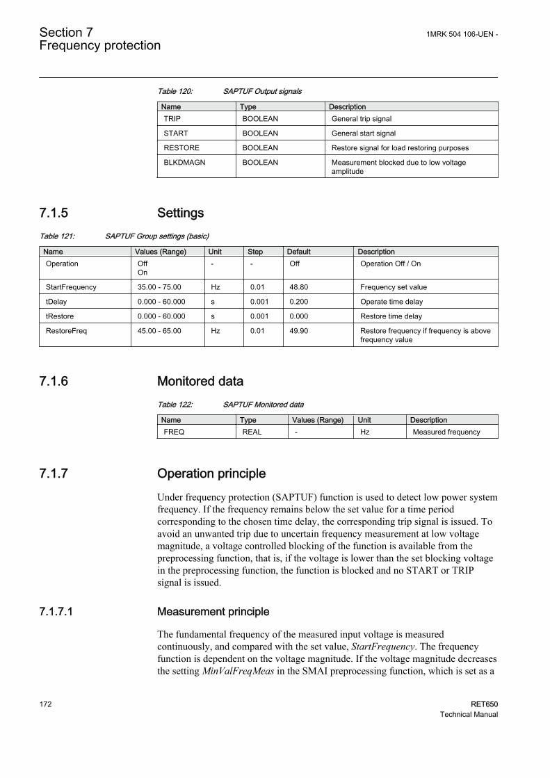
Table 120: SAPTUF Output signals
Name Type DescriptionTRIP BOOLEAN General trip signal
START BOOLEAN General start signal
RESTORE BOOLEAN Restore signal for load restoring purposes
BLKDMAGN BOOLEAN Measurement blocked due to low voltageamplitude
7.1.5 SettingsTable 121: SAPTUF Group settings (basic)
Name Values (Range) Unit Step Default DescriptionOperation Off
On- - Off Operation Off / On
StartFrequency 35.00 - 75.00 Hz 0.01 48.80 Frequency set value
tDelay 0.000 - 60.000 s 0.001 0.200 Operate time delay
tRestore 0.000 - 60.000 s 0.001 0.000 Restore time delay
RestoreFreq 45.00 - 65.00 Hz 0.01 49.90 Restore frequency if frequency is abovefrequency value
7.1.6 Monitored dataTable 122: SAPTUF Monitored data
Name Type Values (Range) Unit DescriptionFREQ REAL - Hz Measured frequency
7.1.7 Operation principleUnder frequency protection (SAPTUF) function is used to detect low power systemfrequency. If the frequency remains below the set value for a time periodcorresponding to the chosen time delay, the corresponding trip signal is issued. Toavoid an unwanted trip due to uncertain frequency measurement at low voltagemagnitude, a voltage controlled blocking of the function is available from thepreprocessing function, that is, if the voltage is lower than the set blocking voltagein the preprocessing function, the function is blocked and no START or TRIPsignal is issued.
7.1.7.1 Measurement principle
The fundamental frequency of the measured input voltage is measuredcontinuously, and compared with the set value, StartFrequency. The frequencyfunction is dependent on the voltage magnitude. If the voltage magnitude decreasesthe setting MinValFreqMeas in the SMAI preprocessing function, which is set as a
Section 7 1MRK 504 106-UEN -Frequency protection
172 RET650Technical Manual

percentage of a global base voltage parameter, SAPTUF gets blocked, and theoutput BLKDMAGN is issued. All voltage settings are made in percent of thesetting of the global parameter UBase.
To avoid oscillations of the output START signal, a hysteresis has been included.
7.1.7.2 Time delay
The time delay for SAPTUF is a settable definite time delay, specified by thesetting tDelay.
Trip signal issuing requires that the under frequency condition continues for at leastthe user set time delay. If the START condition, with respect to the measuredfrequency ceases during the delay time, and is not fulfilled again within a definedreset time, the START output is reset.
On the RESTORE output of SAPTUF a 100 ms pulse is issued, after a time delaycorresponding to the setting of tRestore, when the measured frequency returns tothe level corresponding to the setting RestoreFreq.
7.1.7.3 Blocking
It is possible to block Under frequency protection (SAPTUF) completely, by binaryinput signal:
BLOCK: blocks all outputs
If the measured voltage level decreases below the setting of MinValFreqMeas inthe preprocessing function, both the START and the TRIP outputs, are blocked.
7.1.7.4 Design
The frequency measuring element continuously measures the frequency of thepositive sequence voltage and compares it to the setting StartFrequency. Thefrequency signal is filtered to avoid transients due to switchings and faults in thepower systems. When the frequency has returned back to the setting ofRestoreFreq, the RESTORE output is issued after the time delay tRestore. Thedesign of Under frequency protection (SAPTUF) is schematically described infigure 75.
1MRK 504 106-UEN - Section 7Frequency protection
RET650 173Technical Manual

Frequency Comparatorf < StartFrequency
STARTSTART
TRIP
BLOCK
Comparatorf > RestoreFreq
BLOCK
OR
DefiniteTimeDelay
TimeDlyOperate
TimeDlyRestore RESTORE
100 ms
Start&
TripOutput Logic
IEC09000034-1.vsd
TRIP
BLKDMAGN
freqNotValid
IEC09000034 V1 EN
Figure 75: Schematic design of Under frequency function SAPTUF
7.1.8 Technical dataTable 123: SAPTUF Technical data
Function Range or value AccuracyOperate value, start function (35.00-75.00) Hz ± 2.0 mHz
Operate value, restore frequency (45 - 65) Hz ± 2.0 mHz
Operate time, start function 200 ms typically at fr to 0.99 xfset
-
Reset time, start function 50 ms typically at 1.01 x fset to fr -
Timers (0.000-60.000)s ± 0.5% +10 ms
7.2 Over frequency protection SAPTOF
7.2.1 IdentificationFunction description IEC 61850
identificationIEC 60617identification
ANSI/IEEE C37.2device number
Over frequency protection SAPTOF
f >
SYMBOL-O V1 EN
81
Section 7 1MRK 504 106-UEN -Frequency protection
174 RET650Technical Manual

7.2.2 FunctionalityOver frequency protection (SAPTOF) function is applicable in all situations, wherereliable detection of high fundamental power system frequency is needed.
Over frequency occurs at sudden load drops or shunt faults in the power network.Close to the generating plant, generator governor problems can also cause overfrequency.
SAPTOF is used mainly for generation shedding and remedial action schemes. It isalso used as a frequency stage initiating load restoring.
SAPTOF is provided with an under voltage blocking.
7.2.3 Function blockSAPTOF
U3P*BLOCK
TRIPSTART
BLKDMAGN
IEC09000280_1_en.vsdIEC09000280 V1 EN
Figure 76: SAPTOF function block
7.2.4 SignalsTable 124: SAPTOF Input signals
Name Type Default DescriptionU3P GROUP
SIGNAL- Three phase group signal for voltage inputs
BLOCK BOOLEAN 0 Block of function
Table 125: SAPTOF Output signals
Name Type DescriptionTRIP BOOLEAN General trip signal
START BOOLEAN General start signal
BLKDMAGN BOOLEAN Measurement blocked due to low amplitude
1MRK 504 106-UEN - Section 7Frequency protection
RET650 175Technical Manual

7.2.5 SettingsTable 126: SAPTOF Group settings (basic)
Name Values (Range) Unit Step Default DescriptionOperation Off
On- - Off Operation Off / On
StartFrequency 35.00 - 75.00 Hz 0.01 51.20 Frequency set value
tDelay 0.000 - 60.000 s 0.001 0.200 Operate time delay
7.2.6 Monitored dataTable 127: SAPTOF Monitored data
Name Type Values (Range) Unit DescriptionFREQ REAL - Hz Measured frequency
7.2.7 Operation principleOver frequency protection (SAPTOF) is used to detect high power systemfrequency. SAPTOF has a settable definite time delay. If the frequency remainsabove the set value for a time period corresponding to the chosen time delay, thecorresponding TRIP signal is issued. To avoid an unwanted TRIP due to uncertainfrequency measurement at low voltage magnitude, a voltage controlled blocking ofthe function is available from the preprocessing function, that is, if the voltage islower than the set blocking voltage in the preprocessing function, the function isblocked and no START or TRIP signal is issued.
7.2.7.1 Measurement principle
The fundamental frequency of the positive sequence voltage is measuredcontinuously, and compared with the set value, StartFrequency. Over frequencyprotection (SAPTOF) is dependent on the voltage magnitude. If the voltagemagnitude decreases below the setting MinValFreqMeas in the SMAIpreprocessing function, which is set as a percentage of a global base voltageparameter UBase, SAPTOF is blocked, and the output BLKDMAGN is issued. Allvoltage settings are made in percent of the global parameter UBase. To avoidoscillations of the output START signal, a hysteresis has been included.
7.2.7.2 Time delay
The time delay for SAPTOF is a settable definite time delay, specified by thesetting tDelay.
TRIP signal issuing requires that the over frequency condition continues for at leastthe user set time delay. If the START condition, with respect to the measured
Section 7 1MRK 504 106-UEN -Frequency protection
176 RET650Technical Manual

frequency ceases during the delay time, and is not fulfilled again within a definedreset time, the START output is reset.
7.2.7.3 Blocking
It is possible to block Over frequency protection (SAPTOF) completely, by binaryinput signals or by parameter settings, where:
BLOCK: blocks all outputs
If the measured voltage level decreases below the setting of MinValFreqMeas inthe preprocessing function SMAI, both the START and the TRIP outputs, are blocked.
7.2.7.4 Design
The frequency measuring element continuously measures the frequency of thepositive sequence voltage and compares it to the setting StartFrequency. Thefrequency signal is filtered to avoid transients due to switchings and faults in thepower system. The design of Over frequency protection (SAPTOF) isschematically described in figure 77.
START START
TRIP
Start&
TripOutput Logic
Definite Time Delay
TimeDlyOperate
BLOCK
IEC09000033-1.vsd
Frequency Comparatorf > StartFrequency
TRIP
BLKDMAGN
BLOCK
ORfreqNotValid
IEC09000033 V1 EN
Figure 77: Schematic design of Over frequency protection (SAPTOF)
1MRK 504 106-UEN - Section 7Frequency protection
RET650 177Technical Manual

7.2.8 Technical dataTable 128: SAPTOF Technical data
Function Range or value AccuracyOperate value, start function (35.00-75.00) Hz ± 2.0 mHz at symmetrical three-
phase voltage
Operate time, start function 200 ms typically at fr to 1.01 x fset -
Reset time, start function 50 ms typically at 1.01 x fset to fr -
Timer (0.000-60.000)s ± 0.5% + 10 ms
7.3 Rate-of-change frequency protection SAPFRC
7.3.1 IdentificationFunction description IEC 61850
identificationIEC 60617identification
ANSI/IEEE C37.2device number
Rate-of-change frequency protection SAPFRC
df/dt ><
SYMBOL-N V1 EN
81
7.3.2 FunctionalityRate-of-change frequency protection (SAPFRC) function gives an early indicationof a main disturbance in the system. It can be used for generation shedding, loadshedding, remedial action schemes etc. SAPFRC can discriminate between positiveor negative change of frequency.
7.3.3 Function blockSAPFRC
U3P*BLOCK
TRIPSTART
RESTOREBLKDMAGN
IEC09000281_1_en.vsdIEC09000281 V1 EN
Figure 78: SAPFRC function block
Section 7 1MRK 504 106-UEN -Frequency protection
178 RET650Technical Manual

7.3.4 SignalsTable 129: SAPFRC Input signals
Name Type Default DescriptionU3P GROUP
SIGNAL- Three phase group signal for voltage inputs
BLOCK BOOLEAN 0 Block of function
Table 130: SAPFRC Output signals
Name Type DescriptionTRIP BOOLEAN Operate/trip signal for frequency gradient
START BOOLEAN Start/pick-up signal for frequency gradient
RESTORE BOOLEAN Restore signal for load restoring purposes
BLKDMAGN BOOLEAN Blocking indication due to low amplitude
7.3.5 SettingsTable 131: SAPFRC Group settings (basic)
Name Values (Range) Unit Step Default DescriptionOperation Off
On- - Off Operation Off / On
StartFreqGrad -10.00 - 10.00 Hz/s 0.01 0.50 Frequency gradient start value, the signdefines direction
tTrip 0.000 - 60.000 s 0.001 0.200 Operate time delay in positive / negativefrequency gradient mode
RestoreFreq 45.00 - 65.00 Hz 0.01 49.90 Restore is enabled if frequency is aboveset frequency value
tRestore 0.000 - 60.000 s 0.001 0.000 Restore time delay
7.3.6 Operation principleRate-of-change frequency protection (SAPFRC) is used to detect fast power systemfrequency changes, increase as well as, decrease at an early stage. SAPFRC has asettable definite time delay. If the rate-of-change of frequency remains below theset value, for negative rate-of-change, for a time period equal to the chosen timedelay, the TRIP signal is issued. If the rate-of-change of frequency remains abovethe set value, for positive rate-of-change, for a time period equal to the chosen timedelay, the TRIP signal is issued. To avoid an unwanted trip due to uncertainfrequency measurement at low voltage magnitude, a voltage controlled blocking ofthe function is available from the preprocessing function that is, if the voltage islower than the set blocking voltage in the preprocessing function, the function isblocked and no START or TRIP signal is issued. If the frequency recovers, after afrequency decrease, a restore signal is issued.
1MRK 504 106-UEN - Section 7Frequency protection
RET650 179Technical Manual

7.3.6.1 Measurement principle
The rate-of-change of the fundamental frequency of the selected voltage ismeasured continuously, and compared with the set value, StartFreqGrad. Rate-of-change frequency protection (SAPFRC) is also dependent on the voltagemagnitude. If the voltage magnitude decreases below the setting MinValFreqMeasin the preprocessing function,which is set as a percentage of a global base voltageparameter, SAPFRC is blocked, and the output BLKDMAGN is issued. The signof the setting StartFreqGrad, controls if SAPFRC function reacts on a positive oron a negative change in frequency. If SAPFRC is used for decreasing frequencythat is, the setting StartFreqGrad has been given a negative value, and a trip signalhas been issued, then a 100 ms pulse is issued on the RESTORE output, when thefrequency recovers to a value higher than the setting RestoreFreq. A positivesetting of StartFreqGrad, sets SAPFRC function to START and TRIP forfrequency increases.
To avoid oscillations of the output START signal, a hysteresis has been included.
7.3.6.2 Time delay
SAPFRC has a settable definite time delay, tTrip.
Trip signal issuing requires that SAPFRC condition continues for at least the userset time delay, tTrip. If the START condition, with respect to the measuredfrequency ceases during the delay time, and is not fulfilled again within a definedreset time, the START output is reset after the reset time has elapsed.
The RESTORE output of SAPFRC function is set, after a time delay equal to thesetting of tRestore, when the measured frequency has returned to the levelcorresponding to RestoreFreq, after an issue of the TRIP output signal. If tRestoreis set to 0.000 s the restore functionality is disabled, and no output will be given.The restore functionality is only active for lowering frequency conditions and therestore sequence is disabled if a new negative frequency gradient is detected duringthe restore period, defined by the settings RestoreFreq and tRestore.
Section 7 1MRK 504 106-UEN -Frequency protection
180 RET650Technical Manual

7.3.6.3 Design
IEC08000009_en_1.vsd
RESTORE
START START
TRIP
Start&
TripOutput Logic
BLOCK
Frequency
100 ms
ComparatorIf
[StartFreqGrad<0AND
df/dt < StartFreqGrad]OR
[StartFreqGrad>0AND
df/dt > StartFreqGrad]Then
START
Comparatorf > RestoreFreq
OR
Definite Time Delay
tTrip
tRestore
BLKDMAGN
Rate-of-Changeof Frequency
BLOCK
freqNotValid
IEC08000009 V1 EN
Figure 79: Schematic design of Rate-of-change frequency protection (SAPFRC)
7.3.7 Technical dataTable 132: SAPFRC Technical data
Function Range or value AccuracyOperate value, start function (-10.00-10.00) Hz/s ± 10.0 mHz/s
Operate value, restoreenable frequency
(45.00 - 65.00) Hz
Timers (0.000 - 60.000) s ± 0.5% + 10 ms
Operate time, start function 100 ms typically -
1MRK 504 106-UEN - Section 7Frequency protection
RET650 181Technical Manual

182

Section 8 Secondary system supervision
8.1 Breaker close/trip circuit monitoring TCSSCBR
8.1.1 Identification
Function description IEC 61850identification
IEC 60617identification
ANSI/IEEE C37.2device number
Trip circuit supervision TCSSCBR - -
8.1.2 FunctionalityThe trip circuit supervision function TCSSCBR is designed to supervise the controlcircuit of the circuit breaker. The invalidity of a control circuit is detected by usinga dedicated output contact that contains the supervision functionality.
The function operates after a predefined operating time and resets when the faultdisappears.
The function contains a blocking functionality. Blocking deactivates the ALARMoutput and resets the timer.
8.1.3 Function block
GUID-6F85BD70-4D18-4A00-A410-313233025F3A V2 EN
Figure 80: Function block
8.1.4 SignalsTable 133: TCSSCBR Input signals
Name Type Default DescriptionTCS_STATE BOOLEAN 0 Trip circuit fail indication from I/O-card
BLOCK BOOLEAN 0 Block of function
1MRK 504 106-UEN - Section 8Secondary system supervision
RET650 183Technical Manual

Table 134: TCSSCBR Output signals
Name Type DescriptionALARM BOOLEAN Trip circuit fault indication
8.1.5 SettingsTable 135: TCSSCBR Non group settings (basic)
Name Values (Range) Unit Step Default DescriptionOperation Off
On- - On Operation Off/On
tDelay 0.020 - 300.000 s 0.001 3.000 Operate time delay
8.1.6 Monitored dataTable 136: TCSSCBR Monitored data
Name Type Values (Range) Unit DescriptionALARM BOOLEAN 0=FALSE
1=TRUE- Trip circuit fault indication
8.1.7 Operation principleThe function can be enabled and disabled with the Operation setting. Thecorresponding parameter values are "On" and "Off".
The operation of trip circuit supervision can be described by using a modulediagram. All the modules in the diagram are explained in the next sections.
GUID-9D3B79CB-7E06-4260-B55F-B7FA004CB2AC V1 EN
Figure 81: Functional module diagram
Trip circuit supervision generates a current of approximately 1.0mA through the supervised circuit. It must be ensured that thiscurrent will not cause a latch up of the controlled object.
Section 8 1MRK 504 106-UEN -Secondary system supervision
184 RET650Technical Manual

To protect the trip circuit supervision circuits in the IED, the outputcontacts are provided with parallel transient voltage suppressors.The breakdown voltage of these suppressors is 400 +/– 20 V DC.
TimerOnce activated, the timer runs until the set value tDelay is elapsed. The timecharacteristic is according to DT. When the operation timer has reached themaximum time value, the ALARM output is activated. If a drop-off situation occursduring the operate time up counting, the reset timer is activated.
The binary input BLOCK can be used to block the function. The activation of theBLOCK input deactivates the ALARM output and resets the internal timer.
8.1.8 Technical dataTable 137: TCSSCBR Technical data
Function Range or value AccuracyOperate time delay (0.020 - 300.000)s ± 0,5% ± 10ms
1MRK 504 106-UEN - Section 8Secondary system supervision
RET650 185Technical Manual

186

Section 9 Control
9.1 Apparatus control APC
9.1.1 FunctionalityThe apparatus control is a function for control and supervision of circuit breakers,disconnectors and earthing switches within a bay. Permission to operate is givenafter evaluation of conditions from other functions such as interlocking,synchrocheck, operator place selection and external or internal blockings.
9.1.2 Bay control QCBAY
9.1.2.1 Identification
Function description IEC 61850identification
IEC 60617identification
ANSI/IEEE C37.2device number
Bay control QCBAY - -
9.1.2.2 Functionality
The bay control (QCBAY) function is used to handle the selection of the operatorplace per bay. QCBAY also provides blocking functions that can be distributed todifferent apparatuses within the bay.
9.1.2.3 Function blockQCBAY
LR_OFFLR_LOCLR_REMLR_VALIDBL_UPDBL_CMD
PSTOUPD_BLKDCMD_BLKD
LOCREM
IEC09000080_1_en.vsd
IEC09000080 V1 EN
Figure 82: QCBAY function block
1MRK 504 106-UEN - Section 9Control
RET650 187Technical Manual

9.1.2.4 Signals
Table 138: QCBAY Input signals
Name Type Default DescriptionLR_OFF BOOLEAN 0 External Local/Remote switch is in Off position
LR_LOC BOOLEAN 0 External Local/Remote switch is in Local position
LR_REM BOOLEAN 0 External Local/Remote switch is in Remoteposition
LR_VALID BOOLEAN 0 Data representing the L/R switch position is valid
BL_UPD BOOLEAN 0 Steady signal to block the position updates
BL_CMD BOOLEAN 0 Steady signal to block the command
Table 139: QCBAY Output signals
Name Type DescriptionPSTO INTEGER Value for the operator place allocation
UPD_BLKD BOOLEAN Update of position is blocked
CMD_BLKD BOOLEAN Function is blocked for commands
LOC BOOLEAN Local operation allowed
REM BOOLEAN Remote operation allowed
9.1.2.5 Settings
Table 140: QCBAY Non group settings (basic)
Name Values (Range) Unit Step Default DescriptionAllPSTOValid Priority
No priority- - Priority Priority of originators
9.1.3 Local remote LOCREM
9.1.3.1 Identification
Function description IEC 61850identification
IEC 60617identification
ANSI/IEEE C37.2device number
Local remote LOCREM - -
9.1.3.2 Functionality
The signals from the local HMI or from an external local/remote switch are appliedvia function blocks LOCREM and LOCREMCTRL to the Bay control (QCBAY)function block. A parameter in function block LOCREM is set to choose if theswitch signals are coming from the local HMI or from an external hardware switchconnected via binary inputs.
Section 9 1MRK 504 106-UEN -Control
188 RET650Technical Manual

9.1.3.3 Function blockLOCREM
CTRLOFFLOCCTRLREMCTRLLHMICTRL
OFFLOCAL
REMOTEVALID
IEC09000076_1_en.vsd
IEC09000076 V1 EN
Figure 83: LOCREM function block
9.1.3.4 Signals
Table 141: LOCREM Input signals
Name Type Default DescriptionCTRLOFF BOOLEAN 0 Disable control
LOCCTRL BOOLEAN 0 Local in control
REMCTRL BOOLEAN 0 Remote in control
LHMICTRL INTEGER 0 LHMI control
Table 142: LOCREM Output signals
Name Type DescriptionOFF BOOLEAN Control is disabled
LOCAL BOOLEAN Local control is activated
REMOTE BOOLEAN Remote control is activated
VALID BOOLEAN Outputs are valid
9.1.3.5 Settings
Table 143: LOCREM Non group settings (basic)
Name Values (Range) Unit Step Default DescriptionControlMode Internal LR-switch
External LR-switch- - Internal LR-switch Control mode for internal/external LR-
switch
9.1.4 Local remote control LOCREMCTRL
9.1.4.1 Identification
Function description IEC 61850identification
IEC 60617identification
ANSI/IEEE C37.2device number
Local remote control LOCREMCTRL - -
1MRK 504 106-UEN - Section 9Control
RET650 189Technical Manual

9.1.4.2 Functionality
The signals from the local HMI or from an external local/remote switch are appliedvia function blocks LOCREM and LOCREMCTRL to the Bay control (QCBAY)function block. A parameter in function block LOCREM is set to choose if theswitch signals are coming from the local HMI or from an external hardware switchconnected via binary inputs.
9.1.4.3 Function block
IEC09000074_1_en.vsd
LOCREMCTRL^PSTO1^PSTO2^PSTO3^PSTO4^PSTO5^PSTO6^PSTO7^PSTO8^PSTO9^PSTO10^PSTO11^PSTO12
^HMICTR1^HMICTR2^HMICTR3^HMICTR4^HMICTR5^HMICTR6^HMICTR7^HMICTR8^HMICTR9
^HMICTR10^HMICTR11^HMICTR12
IEC09000074 V1 EN
Figure 84: LOCREMCTRL function block
9.1.4.4 Signals
Table 144: LOCREMCTRL Input signals
Name Type Default DescriptionPSTO1 INTEGER 0 PSTO input channel 1
PSTO2 INTEGER 0 PSTO input channel 2
PSTO3 INTEGER 0 PSTO input channel 3
PSTO4 INTEGER 0 PSTO input channel 4
PSTO5 INTEGER 0 PSTO input channel 5
PSTO6 INTEGER 0 PSTO input channel 6
PSTO7 INTEGER 0 PSTO input channel 7
PSTO8 INTEGER 0 PSTO input channel 8
PSTO9 INTEGER 0 PSTO input channel 9
PSTO10 INTEGER 0 PSTO input channel 10
PSTO11 INTEGER 0 PSTO input channel 11
PSTO12 INTEGER 0 PSTO input channel 12
Section 9 1MRK 504 106-UEN -Control
190 RET650Technical Manual

Table 145: LOCREMCTRL Output signals
Name Type DescriptionHMICTR1 INTEGER Bitmask output 1 to local remote LHMI input
HMICTR2 INTEGER Bitmask output 2 to local remote LHMI input
HMICTR3 INTEGER Bitmask output 3 to local remote LHMI input
HMICTR4 INTEGER Bitmask output 4 to local remote LHMI input
HMICTR5 INTEGER Bitmask output 5 to local remote LHMI input
HMICTR6 INTEGER Bitmask output 6 to local remote LHMI input
HMICTR7 INTEGER Bitmask output 7 to local remote LHMI input
HMICTR8 INTEGER Bitmask output 8 to local remote LHMI input
HMICTR9 INTEGER Bitmask output 9 to local remote LHMI input
HMICTR10 INTEGER Bitmask output 10 to local remote LHMI input
HMICTR11 INTEGER Bitmask output 11 to local remote LHMI input
HMICTR12 INTEGER Bitmask output 12 to local remote LHMI input
9.1.4.5 Settings
The function does not have any parameters available in Local HMI or Protectionand Control IED Manager (PCM600).
9.1.5 Operation principle
9.1.5.1 Bay control QCBAY
The functionality of the Bay control (QCBAY) function is not defined in the IEC61850–8–1 standard, which means that the function is a vendor specific logical node.
The function sends information about the Permitted Source To Operate (PSTO)and blocking conditions to other functions within the bay for example, switchcontrol functions, voltage control functions and measurement functions.
Local panel switchThe local panel switch is a switch that defines the operator place selection. Theswitch connected to this function can have three positions remote/local/off. Thepositions are here defined so that remote means that operation is allowed from station/remote level and local from the IED level. The local/remote switch is normallysituated on the control/protection IED itself, which means that the position of theswitch and its validity information are connected internally, and not via I/O boards.When the switch is mounted separately on the IED the signals are connected to thefunction via I/O boards.
When the local panel switch is in Off position all commands from remote and locallevel will be ignored. If the position for the local/remote switch is not valid thePSTO output will always be set to faulty state (3), which means no possibility tooperate.
1MRK 504 106-UEN - Section 9Control
RET650 191Technical Manual

To adapt the signals from the local HMI or from an external local/remote switch,the function blocks LOCREM and LOCREMCTRL are needed and connected toQCBAY.
Permitted Source To Operate (PSTO)The actual state of the operator place is presented by the value of the PermittedSource To Operate, PSTO signal. The PSTO value is evaluated from the local/remote switch position according to table 146. In addition, there is oneconfiguration parameter that affects the value of the PSTO signal. If the parameterAllPSTOValid is set and LR-switch position is in Local or Remote state, the PSTOvalue is set to 5 (all), that is, it is permitted to operate from both local and remotelevel without any priority. When the external panel switch is in Off position thePSTO value shows the actual state of switch that is, 0. In this case it is not possibleto control anything.
Table 146: PSTO values for different Local panel switch positions
Local panel switchpositions
PSTO value AllPSTOValid(configurationparameter)
Possible locations that shall be able tooperate
0 = Off 0 -- Not possible to operate
1 = Local 1 FALSE Local Panel
1 = Local 5 TRUE Local or Remote level without anypriority
2 = Remote 2 FALSE Remote level
2 = Remote 5 TRUE Local or Remote level without anypriority
3 = Faulty 3 -- Not possible to operate
BlockingsThe blocking states for position indications and commands are intended to providethe possibility for the user to make common blockings for the functions configuredwithin a complete bay.
The blocking facilities provided by the bay control function are the following:
• Blocking of position indications, BL_UPD. This input will block all inputsrelated to apparatus positions for all configured functions within the bay.
• Blocking of commands, BL_CMD. This input will block all commands for allconfigured functions within the bay.
• Blocking of function, BLOCK, signal from DO (Data Object) Behavior (IEC61850–8–1). If DO Behavior is set to "blocked" it means that the function isactive, but no outputs are generated, no reporting, control commands arerejected and functional and configuration data is visible.
The switching of the Local/Remote switch requires at least system operator level.The password will be requested at an attempt to operate if authority levels have
Section 9 1MRK 504 106-UEN -Control
192 RET650Technical Manual

been defined in the IED. Otherwise the default authority level, SuperUser, canhandle the control without LogOn. The users and passwords are defined in PCM600.
9.1.5.2 Local remote/Local remote control LOCREM/LOCREMCTRL
The function block Local remote (LOCREM) handles the signals coming from thelocal/remote switch. The connections are seen in figure 85, where the inputs onfunction block LOCREM are connected to binary inputs if an external switch isused. When a local HMI is used, the inputs are not used and are set to FALSE inthe configuration. The outputs from the LOCREM function block control theoutput PSTO (Permitted Source To Operate) on Bay control (QCBAY).
LOCREMCTRLPSTO1PSTO2PSTO3PSTO4PSTO5PSTO6PSTO7PSTO8PSTO9PSTO10PSTO11PSTO12
HMICTR1HMICTR2HMICTR3HMICTR4HMICTR5HMICTR6HMICTR7HMICTR8HMICTR9
HMICTR10HMICTR11HMICTR12
QCBAYLR_OFFLR_LOCLR_REMLR_VALIDBL_UPDBL_CMD
PSTOUPD_BLKDCMD_BLKD
LOCREMCTRLOFFLOCCTRLREMCTRLLHMICTRL
OFFLOCAL
REMOTEVALID
IEC09000208_1_en.vsd
LOCREM
IEC09000208 V1 EN
Figure 85: Configuration for the local/remote handling for a local HMI with twobays and two screen pages
The switching of the local/remote switch requires at least system operator level.The password will be requested at an attempt to operate if authority levels havebeen defined in the IED. Otherwise the default authority level, SuperUser, canhandle the control without LogOn. The users and passwords are defined in PCM600.
9.2 Voltage control
9.2.1 FunctionalityThe voltage control functions (Automatic voltage control for tap changer, singlecontrol (TR1ATCC), Automatic voltage control for tap changer, parallel control(TR8ATCC) and Tap changer control and supervision, 6 binary inputs(TCMYLTC) are used for control of power transformers with a motor driven on-load tap changer. The function provides automatic regulation of the voltage on thesecondary side of transformers or alternatively on a load point further out in thenetwork.
1MRK 504 106-UEN - Section 9Control
RET650 193Technical Manual

Control of a single transformer, as well as control of up to two transformers inparallel is possible. For parallel control of power transformers, three alternativemethods are available, the master-follower method, the circulating current methodand the reverse reactance method.
The voltage control includes many extra features such as possibility of to avoidsimultaneous tapping of parallel transformers, hot stand by regulation of atransformer in a group which regulates it to a correct tap position even though theLV CB is open, compensation for a possible capacitor bank on the LV side bay of atransformer, extensive tap changer monitoring including contact wear and huntingdetection, monitoring of the power flow in the transformer so that for example, thevoltage control can be blocked if the power reverses etc.
In manual operating mode it is possible to give raise or lower commands to the on-load tap changer.
The Automatic voltage control for tap changer, (TR1ATCC for single control andTR8ATCC for parallel control) function controls the voltage on the LV side of atransformer either automatically or manually. The automatic control can be eitherfor a single transformer, or for a group of parallel transformers.
The Tap changer control and supervision, 6 binary inputs (TCMYLTC) functiongives the tap commands to the tap changer, and supervises that commands arecarried through correctly. It has built-in extensive possibilities for tap changerposition measurement, as well as supervisory and monitoring features. This is usedin the voltage control and can also give information about tap position to thetransformer differential protection.
9.2.2 Automatic voltage control for tap changer, single control(TR1ATCC)
9.2.2.1 Identification
Function description IEC 61850identification
IEC 60617identification
ANSI/IEEE C37.2device number
Automatic voltage control for tapchanger, single control
TR1ATCC - 90
Section 9 1MRK 504 106-UEN -Control
194 RET650Technical Manual

9.2.2.2 Function blockTR1ATCC
I3P1*I3P2*U3P2*ATCCIN*BLOCKMANCTRLAUTOCTRLPSTORAISEVLOWERVEAUTOBLKDEBLKAUTLVA1LVA2LVA3LVA4LVARESETRSTERR
ATCCOUTMAN
AUTOIBLK
PGTFWDPLTREV
QGTFWDQLTREV
UHIGHULOWUBLK
HOURHUNTDAYHUNTHUNTINGTIMERON
TOTBLKAUTOBLK
UGTUPPDBULTLOWDB
IEC09000324_1_en.vsd
IEC09000324 V1 EN
Figure 86: TR1ATCC function block
9.2.2.3 Signals
Table 147: TR1ATCC Input signals
Name Type Default DescriptionI3P1 GROUP
SIGNAL- Three phase group signal for current on HV side
I3P2 GROUPSIGNAL
- Three phase group signal for current on LV side
U3P2 GROUPSIGNAL
- Three phase group signal for voltage on LV side
ATCCIN GROUPSIGNAL
- Group connection from YLTCOUT
BLOCK BOOLEAN 0 Block of function
MANCTRL BOOLEAN 0 Binary "MAN" command
AUTOCTRL BOOLEAN 0 Binary "AUTO" command
PSTO INTEGER 0 Operator place selection
RAISEV BOOLEAN 0 Binary "UP" command
LOWERV BOOLEAN 0 Binary "DOWN" command
EAUTOBLK BOOLEAN 0 Block the voltage control in automatic control mode
DEBLKAUT BOOLEAN 0 Binary "Deblock Auto" command
LVA1 BOOLEAN 0 Activation of load voltage adjustment factor 1
LVA2 BOOLEAN 0 Activation of load voltage adjustment factor 2
LVA3 BOOLEAN 0 Activation of load voltage adjustment factor 3
LVA4 BOOLEAN 0 Activation of load voltage adjustment factor 4
LVARESET BOOLEAN 0 Reset LVA
RSTERR BOOLEAN 0 Resets automatic control commands
1MRK 504 106-UEN - Section 9Control
RET650 195Technical Manual

Table 148: TR1ATCC Output signals
Name Type DescriptionATCCOUT GROUP SIGNAL Group connection to YLTCIN
MAN BOOLEAN Control is in manual mode
AUTO BOOLEAN Automatic control mode is active
IBLK BOOLEAN One phase current is above the set limit
PGTFWD BOOLEAN Active power above the set limit powerActiveForw
PLTREV BOOLEAN Active power below the set limit powerActiveRev
QGTFWD BOOLEAN Reactive power above the set limitpowerReactiveForw
QLTREV BOOLEAN Reactive power below the set limitpowerReactiveRev
UHIGH BOOLEAN Busbar voltage above the set limitvoltBusbMaxLimit
ULOW BOOLEAN Busbar voltage below the set limitvoltBusbMinLimit
UBLK BOOLEAN Busbar voltage below the set limitvoltBusbBlockLimit
HOURHUNT BOOLEAN Number of commands within the latest hourexceeded maximum level
DAYHUNT BOOLEAN Number of commands within the last 24 hoursexceeded maximum level
HUNTING BOOLEAN Number of commands in opposite directionexceeded maximum level
TIMERON BOOLEAN Raise or lower command to the tap activated
TOTBLK BOOLEAN Block of auto and manual commands
AUTOBLK BOOLEAN Block of auto commands
UGTUPPDB BOOLEAN Voltage greater than deadband-high, ULOWERcommand to come
ULTLOWDB BOOLEAN Voltage lower than deadband-low, URAISEcommand to come
9.2.2.4 Settings
Table 149: TR1ATCC Group settings (basic)
Name Values (Range) Unit Step Default DescriptionOperation Off
On- - Off Operation Off / On
MeasMode L1L2L3L1L2L2L3L3L1PosSeq
- - PosSeq Selection of measured voltage andcurrent
TotalBlock OffOn
- - Off Total block of the voltage control function
Table continues on next page
Section 9 1MRK 504 106-UEN -Control
196 RET650Technical Manual

Name Values (Range) Unit Step Default DescriptionAutoBlock Off
On- - Off Block of the automatic mode in voltage
control function
FastStpDwnMode OffAutoAutoMan
- - Off Fast step down function activation mode
tFastStpDwn 1.0 - 100.0 s 0.1 15.0 Time delay for lower command whenfast step down mode is activated
USet 85.0 - 120.0 %UB2 0.1 100.0 Voltage control set voltage, in % of ratedvoltage
UDeadband 0.2 - 9.0 %UB2 0.1 1.2 Outer voltage deadband, in % of ratedvoltage
UDeadbandInner 0.1 - 9.0 %UB2 0.1 0.9 Inner voltage deadband, in % of ratedvoltage
Umax 80 - 180 %UB2 1 105 Upper limit of busbar voltage, in % ofrated voltage
Umin 70 - 120 %UB2 1 80 Lower limit of busbar voltage, in % ofrated voltage
Ublock 50 - 120 %UB2 1 80 Undervoltage block level, in % of ratedvoltage
t1Use ConstantInverse
- - Constant Activation of long inverse time delay
t1 3 - 1000 s 1 60 Time delay (long) for automatic controlcommands
t2Use ConstantInverse
- - Constant Activation of short inverse time delay
t2 1 - 1000 s 1 15 Time delay (short) for automatic controlcommands
tMin 3 - 120 s 1 5 Minimum operating time in inverse mode
OperationLDC OffOn
- - Off Operation line voltage drop compensation
OperCapaLDC OffOn
- - Off LDC compensation for capacitive load
Rline 0.00 - 150.00 ohm 0.01 0.0 Line resistance, primary values, in ohm
Xline -150.00 - 150.00 ohm 0.01 0.0 Line reactance, primary values, in ohm
LVAConst1 -20.0 - 20.0 %UB2 0.1 0.0 Constant 1 for LVA, % of regulatedvoltage
LVAConst2 -20.0 - 20.0 %UB2 0.1 0.0 Constant 2 for LVA, % of regulatedvoltage
LVAConst3 -20.0 - 20.0 %UB2 0.1 0.0 Constant 3 for LVA, % of regulatedvoltage
LVAConst4 -20.0 - 20.0 %UB2 0.1 0.0 Constant 4 for LVA, % of regulatedvoltage
VRAuto -20.0 - 20.0 %UB2 0.1 0.0 Load voltage auto correction, in % ofrated voltage
Iblock 0 - 250 %IB1 1 150 Overcurrent block level, in % of ratedcurrent
HourHuntDetect 0 - 30 Op/H 1 30 Level for number of counted raise/lowerwithin one hour
Table continues on next page
1MRK 504 106-UEN - Section 9Control
RET650 197Technical Manual

Name Values (Range) Unit Step Default DescriptionDayHuntDetect 0 - 100 Op/D 1 100 Level for number of counted raise/lower
within 24 hour
tWindowHunt 1 - 120 Min 1 60 Time window for hunting alarm, minutes
NoOpWindow 3 - 30 Op/W 1 30 Hunting detection alarm, maximumoperations/window
P> -9999.99 - 9999.99 MW 0.01 1000 Alarm level of active power in forwarddirection
P< -9999.99 - 9999.99 MW 0.01 -1000 Alarm level of active power in reversedirection
Q> -9999.99 - 9999.99 MVAr 0.01 1000 Alarm level of reactive power in forwarddirection
Q< -9999.99 - 9999.99 MVAr 0.01 -1000 Alarm level of reactive power in reversedirection
tPower 1 - 6000 s 1 10 Time delay for alarms from powersupervision
Table 150: TR1ATCC Non group settings (basic)
Name Values (Range) Unit Step Default DescriptionGlobalBaseSel1 1 - 6 - 1 1 Global base selector for winding 1
GlobalBaseSel2 1 - 6 - 1 1 Global base selector for winding 2
Xr2 0.1 - 200.0 ohm 0.1 0.5 Transformer reactance in primary ohmson ATCC side
CmdErrBk AlarmAuto BlockAuto&Man Block
- - Auto Block Alarm, auto block or auto&man block forcommand error
OCBk AlarmAuto BlockAuto&Man Block
- - Auto&Man Block Alarm, auto block or auto&man block forovercurrent
OVPartBk AlarmAuto BlockAuto&Man Block
- - Auto&Man Block Alarm, auto partial or auto&man partialblock for overvoltage
RevActPartBk AlarmAuto Block
- - Alarm Alarm or auto partial block for reverseaction
TapChgBk AlarmAuto BlockAuto&Man Block
- - Auto Block Alarm, auto block or auto&man block fortap changer error
TapPosBk AlarmAuto BlockAuto&Man Block
- - Auto Block Alarm, auto or auto&man block forposition supervision
UVBk AlarmAuto BlockAuto&Man Block
- - Auto Block Alarm, auto block or auto&man block forundervoltage
UVPartBk AlarmAuto BlockAuto&Man Block
- - Auto Block Alarm, auto partial or auto&man partialblock for undervoltage
Section 9 1MRK 504 106-UEN -Control
198 RET650Technical Manual

9.2.2.5 Monitored data
Table 151: TR1ATCC Monitored data
Name Type Values (Range) Unit DescriptionRAISE BOOLEAN - - Raise voltage order to
tapchanger
LOWER BOOLEAN - - Lower voltage order totapchanger
BUSVOLT REAL - kV Average of themeasured busbarvoltage (service value)
VOLTDEV REAL - % Voltage deviationcompared to dead band(%)
TRLDCURR REAL - A Amplitude of own loadcurrent
USETOUT REAL - kV Voltage setpoint used insingle mode (servicevalue)
ULOAD REAL - kV Calculated compensatedvoltage (service value)
P REAL - MW Calculated active power(service value)
Q REAL - MVAr Calculated reactivepower (service value)
IPRIM REAL - A Maximum of 3 phasecurrents (service value)
9.2.3 Automatic voltage control for tap changer, parallel control(TR8ATCC)
9.2.3.1 Identification
Function description IEC 61850identification
IEC 60617identification
ANSI/IEEE C37.2device number
Automatic voltage control for tapchanger, parallel control
TR8ATCC - 90
1MRK 504 106-UEN - Section 9Control
RET650 199Technical Manual

9.2.3.2 Function blockTR8ATCC
I3P1*I3P2*U3P2*HORIZ1*HORIZ2*HORIZ3*HORIZ4*ATCCIN*BLOCKMANCTRLAUTOCTRLPSTORAISEVLOWERVEAUTOBLKDEBLKAUTLVA1LVA2LVA3LVA4LVARESETRSTERRDISCSNGLMODET1INCLDT2INCLDT3INCLDT4INCLDFORCMASTRSTMAST
ATCCOUTMAN
AUTOIBLK
PGTFWDPLTREV
QGTFWDQLTREV
UHIGHULOWUBLK
HOURHUNTDAYHUNTHUNTING
SINGLEPARALLELTIMERON
ADAPTTOTBLK
AUTOBLKMASTER
FOLLOWERMFERR
OUTOFPOSUGTUPPDBULTLOWDBCOMMERR
ICIRCTRFDISC
VTALARMT1PGT2PGT3PGT4PG
IEC09000325_1_en.vsdIEC09000325 V1 EN
Figure 87: TR8ATCC function block
9.2.3.3 Signals
Table 152: TR8ATCC Input signals
Name Type Default DescriptionI3P1 GROUP
SIGNAL- Three phase group signal for current on HV side
I3P2 GROUPSIGNAL
- Three phase group signal for current on LV side
U3P2 GROUPSIGNAL
- Three phase group signal for voltage on LV side
HORIZ1 GROUPSIGNAL
- Group connection for horizontal communicationfrom T1
HORIZ2 GROUPSIGNAL
- Group connection for horizontal communicationfrom T2
HORIZ3 GROUPSIGNAL
- Group connection for horizontal communicationfrom T3
HORIZ4 GROUPSIGNAL
- Group connection for horizontal communicationfrom T4
ATCCIN GROUPSIGNAL
- Group connection from YLTCOUT
BLOCK BOOLEAN 0 Block of function
MANCTRL BOOLEAN 0 Binary "MAN" command
AUTOCTRL BOOLEAN 0 Binary "AUTO" command
PSTO INTEGER 0 Operator place selection
RAISEV BOOLEAN 0 Binary "UP" command
Table continues on next page
Section 9 1MRK 504 106-UEN -Control
200 RET650Technical Manual

Name Type Default DescriptionLOWERV BOOLEAN 0 Binary "DOWN" command
EAUTOBLK BOOLEAN 0 Block voltage control in automatic control mode
DEBLKAUT BOOLEAN 0 Binary "Deblock Auto" command
LVA1 BOOLEAN 0 Activation of load voltage adjustment factor 1
LVA2 BOOLEAN 0 Activation of load voltage adjustment factor 2
LVA3 BOOLEAN 0 Activation of load voltage adjustment factor 3
LVA4 BOOLEAN 0 Activation of load voltage adjustment factor 4
LVARESET BOOLEAN 0 Reset LVA
RSTERR BOOLEAN 0 Resets automatic control commands
DISC BOOLEAN 0 Disconnected transformer
SNGLMODE BOOLEAN 0 Voltage control in single control
T1INCLD BOOLEAN 0 Transformer1 included in parallel group
T2INCLD BOOLEAN 0 Transformer2 included in parallel group
T3INCLD BOOLEAN 0 Transformer3 included in parallel group
T4INCLD BOOLEAN 0 Transformer4 included in parallel group
FORCMAST BOOLEAN 0 Force transformer to master
RSTMAST BOOLEAN 0 Reset forced master transformer to default
Table 153: TR8ATCC Output signals
Name Type DescriptionATCCOUT GROUP SIGNAL Group connection to YLTCIN
MAN BOOLEAN Manual control mode is active
AUTO BOOLEAN Automatic control mode is active
IBLK BOOLEAN One phase current is above the set limit
PGTFWD BOOLEAN Active power above the set limit powerActiveForw
PLTREV BOOLEAN Active power below the set limit powerActiveRev
QGTFWD BOOLEAN Reactive power above the set limitpowerReactiveForw
QLTREV BOOLEAN Reactive power below the set limitpowerReactiveRev
UHIGH BOOLEAN Busbar voltage above the set limitvoltBusbMaxLimit
ULOW BOOLEAN Busbar voltage below the set limitvoltBusbMinLimit
UBLK BOOLEAN Busbar voltage below the set limitvoltBusbBlockLimit
HOURHUNT BOOLEAN Number of commands within the latest hourexceeded maximum level
DAYHUNT BOOLEAN Number of commands within the last 24 hoursexceeded maximum level
HUNTING BOOLEAN Number of commands in opposite directionexceeded maximum level
Table continues on next page
1MRK 504 106-UEN - Section 9Control
RET650 201Technical Manual

Name Type DescriptionSINGLE BOOLEAN Transformer operates in single mode
PARALLEL BOOLEAN Transformer operates in parallel mode
TIMERON BOOLEAN Raise or lower command to the tap activated
ADAPT BOOLEAN Transformer is adapting
TOTBLK BOOLEAN Block of auto and manual commands
AUTOBLK BOOLEAN Block of auto commands
MASTER BOOLEAN Transformer is master
FOLLOWER BOOLEAN This transformer is follower
MFERR BOOLEAN Number of masters is different from one
OUTOFPOS BOOLEAN Difference in tap positions exceeded the set limit
UGTUPPDB BOOLEAN Voltage greater than deadband-high, ULOWERcommand to come
ULTLOWDB BOOLEAN Voltage lower than deadband-low, URAISEcommand to come
COMMERR BOOLEAN Communication error
ICIRC BOOLEAN Block from high circulating current
TRFDISC BOOLEAN Transformer is disconnected
VTALARM BOOLEAN VT supervision alarm
T1PG BOOLEAN Transformer 1 included in parallel group
T2PG BOOLEAN Transformer 2 included in parallel group
T3PG BOOLEAN Transformer 3 included in parallel group
T4PG BOOLEAN Transformer 4 included in parallel group
9.2.3.4 Settings
Table 154: TR8ATCC Group settings (basic)
Name Values (Range) Unit Step Default DescriptionOperation Off
On- - Off Operation Off / On
MeasMode L1L2L3L1L2L2L3L3L1PosSeq
- - PosSeq Selection of measured voltage andcurrent
TotalBlock OffOn
- - Off Total block of the voltage control function
AutoBlock OffOn
- - Off Block of the automatic mode in voltagecontrol function
FSDMode OffAutoAutoMan
- - Off Fast step down function activation mode
tFSD 1.0 - 100.0 s 0.1 15.0 Time delay for lower command whenfast step down mode is activated
Table continues on next page
Section 9 1MRK 504 106-UEN -Control
202 RET650Technical Manual

Name Values (Range) Unit Step Default DescriptionUSet 85.0 - 120.0 %UB2 0.1 100.0 Voltage control set voltage, in % of rated
voltage
UDeadband 0.2 - 9.0 %UB2 0.1 1.2 Outer voltage deadband, in % of ratedvoltage
UDeadbandInner 0.1 - 9.0 %UB2 0.1 0.9 Inner voltage deadband, in % of ratedvoltage
Umax 80 - 180 %UB2 1 105 Upper limit of busbar voltage, in % ofrated voltage
Umin 70 - 120 %UB2 1 80 Lower limit of busbar voltage, in % ofrated voltage
Ublock 50 - 120 %UB2 1 80 Undervoltage block level, % of ratedvoltage
t1Use ConstantInverse
- - Constant Activation of long inverse time delay
t1 3 - 1000 s 1 60 Time delay (long) for automatic controlcommands
t2Use ConstantInverse
- - Constant Activation of short inverse time delay
t2 1 - 1000 s 1 15 Time delay (short) for automatic controlcommands
tMin 3 - 120 s 1 5 Minimum operating time in inverse mode
OperationLDC OffOn
- - Off Operation line voltage drop compensation
OperCapaLDC OffOn
- - Off LDC compensation for capacitive load
Rline 0.00 - 150.00 ohm 0.01 0.0 Line resistance, primary values, in ohm
Xline -150.00 - 150.00 ohm 0.01 0.0 Line reactance, primary values, in ohm
LVAConst1 -20.0 - 20.0 %UB2 0.1 0.0 Constant 1 for LVA, % of regulatedvoltage
LVAConst2 -20.0 - 20.0 %UB2 0.1 0.0 Constant 2 for LVA, % of regulatedvoltage
LVAConst3 -20.0 - 20.0 %UB2 0.1 0.0 Constant 3 for LVA, % of regulatedvoltage
LVAConst4 -20.0 - 20.0 %UB2 0.1 0.0 Constant 4 for LVA, % of regulatedvoltage
VRAuto -20.0 - 20.0 %UB2 0.1 0.0 Load voltage auto correction, in % ofrated voltage
Iblock 0 - 250 %IB1 1 150 Overcurrent block level, in % of ratedcurrent
HourHuntDetect 0 - 30 Op/H 1 30 Level for number of counted raise/lowerwithin one hour
DayHuntDetect 0 - 100 Op/D 1 100 Level for number of counted raise/lowerwithin 24 hour
tWindowHunt 1 - 120 Min 1 60 Time window for hunting alarm, minutes
NoOpWindow 3 - 30 Op/W 1 30 Hunting detection alarm, maximumoperations/window
P> -9999.99 - 9999.99 MW 0.01 1000 Alarm level of active power in forwarddirection
Table continues on next page
1MRK 504 106-UEN - Section 9Control
RET650 203Technical Manual

Name Values (Range) Unit Step Default DescriptionP< -9999.99 - 9999.99 MW 0.01 -1000 Alarm level of active power in reverse
direction
Q> -9999.99 - 9999.99 MVAr 0.01 1000 Alarm level of reactive power in forwarddirection
Q< -9999.99 - 9999.99 MVAr 0.01 -1000 Alarm level of reactive power in reversedirection
tPower 1 - 6000 s 1 10 Time delay for alarms from powersupervision
OperationPAR OffCCMF
- - Off Parallel operation, Off/CirculatingCurrent/MasterFollower
OperCCBlock OffOn
- - On Enable block from circulating currentsupervision
CircCurrLimit 0.0 - 20000.0 %IB2 0.1 100.0 Block level for circulating current
tCircCurr 0 - 1000 s 1 30 Time delay for block from circulatingcurrent
Comp 0 - 2000 % 1 100 Compensation parameter in % forCirculating Current
OperSimTap OffOn
- - Off Simultaneous tapping prohibited
OperUsetPar OffOn
- - Off Use common voltage set point forparallel operation
VTmismatch 0.5 - 10.0 %UB2 0.1 10.0 Alarm level for VT supervision, in % ofrated voltage
tVTmismatch 1 - 600 s 1 10 Time delay for VT supervision alarm
T1RXOP OffOn
- - Off Receive block operation from paralleltransformer 1
T2RXOP OffOn
- - Off Receive block operation from paralleltransformer 2
T3RXOP OffOn
- - Off Receive block operation from paralleltransformer 3
T4RXOP OffOn
- - Off Receive block operation from paralleltransformer 4
TapPosOffs -5 - 5 - 1 0 Tap position offset in relation to the master
MFPosDiffLim 1 - 20 - 1 1 Alarm for tap position difference frommaster
tMFPosDiff 0 - 6000 s 1 60 Time for tap position difference frommaster
Section 9 1MRK 504 106-UEN -Control
204 RET650Technical Manual

Table 155: TR8ATCC Non group settings (basic)
Name Values (Range) Unit Step Default DescriptionGlobalBaseSel1 1 - 6 - 1 1 Selection of one of the Global Base
Value groups, winding 1
GlobalBaseSel2 1 - 6 - 1 1 Selection of one of the Global BaseValue groups, winding 2
TrfId T1T2T3T4
- - T1 Identity of transformer
Xr2 0.1 - 200.0 ohm 0.1 0.5 Transformer reactance in primary ohmson ATCC side
tAutoMSF 0 - 60 s 1 10 Time delay for command for auto follower
OperationAdapt OffOn
- - Off Enable adapt mode
MFMode Follow CmdFollow Tap
- - Follow Cmd Select follow tap or follow command
CircCurrBk AlarmAuto BlockAuto&Man Block
- - Alarm Alarm, auto block or auto&man block forhigh circulating current
CmdErrBk AlarmAuto BlockAuto&Man Block
- - Auto Block Alarm, auto block or auto&man block forcommand error
OCBk AlarmAuto BlockAuto&Man Block
- - Auto&Man Block Alarm, auto block or auto&man block forovercurrent
MFPosDiffBk AlarmAuto Block
- - Auto Block Alarm or auto block for tap positiondifference in MF
OVPartBk AlarmAuto BlockAuto&Man Block
- - Auto&Man Block Alarm, auto partial or auto&man partialblock for overvoltage
RevActPartBk AlarmAuto Block
- - Alarm Alarm or auto partial block for reverseaction
TapChgBk AlarmAuto BlockAuto&Man Block
- - Auto Block Alarm, auto block or auto&man block fortap changer error
TapPosBk AlarmAuto BlockAuto&Man Block
- - Auto Block Alarm, auto or auto&man block forposition supervision
UVBk AlarmAuto BlockAuto&Man Block
- - Auto Block Alarm, auto block or auto&man block forundervoltage
UVPartBk AlarmAuto BlockAuto&Man Block
- - Auto Block Alarm, auto partial or auto&man partialblock for undervoltage
1MRK 504 106-UEN - Section 9Control
RET650 205Technical Manual

9.2.3.5 Monitored data
Table 156: TR8ATCC Monitored data
Name Type Values (Range) Unit DescriptionRAISE BOOLEAN - - Raise voltage order to
tapchanger
LOWER BOOLEAN - - Lower voltage order totapchanger
BUSVOLT REAL - kV Average of measuredbusbar voltage (servicevalue)
VOLTDEV REAL - % Voltage deviationcompared to dead band(%)
TRLDCURR REAL - A Amplitude of own loadcurrent
USETOUT REAL - kV Voltage setpoint used insingle mode (servicevalue)
ULOAD REAL - kV Calculated compensatedvoltage (service value)
P REAL - MW Calculated active power(service value)
Q REAL - MVAr Calculated reactivepower (service value)
IPRIM REAL - A Maximum of 3 phasecurrents (service value)
CCAVolt REAL - kV Circulating currentadjusted voltage
USETPAR REAL - kV Average voltage setpointused in parallel mode
ICIRCUL REAL - A Circulating current
9.2.4 Tap changer control and supervision, 6 binary inputs(TCMYLTC)
9.2.4.1 Identification
Function description IEC 61850identification
IEC 60617identification
ANSI/IEEE C37.2device number
Tap changer control and supervision, 6binary inputs
TCMYLTC - 84
Section 9 1MRK 504 106-UEN -Control
206 RET650Technical Manual

9.2.4.2 Function blockTCMYLTC
YLTCIN*TCINPROGINERRRESETERROUTERRRS_CLCNTRS_OPCNTPARITYBIERRB1B2B3B4B5B6MA
YLTCOUTURAISE
ULOWERHIPOSAL
LOPOSALPOSERRALCMDERRAL
TCERRALPOSOUT
CONVERRNEWPOSHIDIFPOSINVALPOS
TCPOS
IEC09000323_1_en.vsd
IEC09000323 V1 EN
Figure 88: TCMYLTC function block
9.2.4.3 Signals
TCMYLTC has no other input for tap changer position other than,binary in first release of 650 series. Input signal MA is notsupported in the IED.
Table 157: TCMYLTC Input signals
Name Type Default DescriptionYLTCIN GROUP
SIGNAL- Group connection from ATCCOUT
TCINPROG BOOLEAN 0 Indication that tap is moving
INERR BOOLEAN 0 Supervision signal of the input board
RESETERR BOOLEAN 0 Reset of command and tap error
OUTERR BOOLEAN 0 Supervision of the digital output board
RS_CLCNT BOOLEAN 0 Reset of the contact life counter
RS_OPCNT BOOLEAN 0 Resets the operation counter
PARITY BOOLEAN 0 Parity bit from tap changer for the tap position
BIERR BOOLEAN 0 Error bit from tap changer for the tap position
B1 BOOLEAN 0 Bit 1 from tap changer for the tap position
B2 BOOLEAN 0 Bit 2 from tap changer for the tap position
B3 BOOLEAN 0 Bit 3 from tap changer for the tap position
B4 BOOLEAN 0 Bit 4 from tap changer for the tap position
B5 BOOLEAN 0 Bit 5 from tap changer for the tap position
B6 BOOLEAN 0 Bit 6 from tap changer for the tap position
MA REAL 0 mA from tap changer for the tap position
1MRK 504 106-UEN - Section 9Control
RET650 207Technical Manual

Table 158: TCMYLTC Output signals
Name Type DescriptionYLTCOUT GROUP SIGNAL Group connection to ATCCIN
URAISE BOOLEAN Raise voltage command to tap changer
ULOWER BOOLEAN Lower voltage command to tap changer
HIPOSAL BOOLEAN Alarm for tap in the highest volt position
LOPOSAL BOOLEAN Alarm for tap in the lowest volt position
POSERRAL BOOLEAN Alarm that indicates a problem with the positionindication
CMDERRAL BOOLEAN Alarm for a command without an expectedposition change
TCERRAL BOOLEAN Alarm for none or illegal tap position change
POSOUT BOOLEAN Tap position outside range
CONVERR BOOLEAN General tap position conversion error
NEWPOS BOOLEAN A new tap position is reported, 1 sec pulse
HIDIFPOS BOOLEAN Tap position has changed more than one position
INVALPOS BOOLEAN Last position change was an invalid change
TCPOS INTEGER Integer value corresponding to actual tap position
9.2.4.4 Settings
Table 159: TCMYLTC Group settings (basic)
Name Values (Range) Unit Step Default DescriptionOperation Off
On- - Off Operation Off / On
tTCTimeout 1 - 120 s 1 5 Tap changer constant time-out
tPulseDur 0.5 - 10.0 s 0.1 1.5 Raise/lower command output pulseduration
Table 160: TCMYLTC Non group settings (basic)
Name Values (Range) Unit Step Default DescriptionGlobalBaseSel 1 - 6 - 1 1 Global Base Selector
LowVoltTap 1 - 63 - 1 1 Tap position for the lowest voltage
HighVoltTap 1 - 63 - 1 33 Tap position for the highest voltage
mALow 0.000 - 25.000 mA 0.001 4.000 mA for the lowest voltage tap position
mAHigh 0.000 - 25.000 mA 0.001 20.000 mA for the highest voltage tap position
CodeType BinaryBCDGrayContactPerTapmA
- - Binary Type of code conversion
UseParity OffOn
- - Off Enable parity check
Table continues on next page
Section 9 1MRK 504 106-UEN -Control
208 RET650Technical Manual

Name Values (Range) Unit Step Default DescriptiontStable 1 - 60 s 1 2 Time after position change before the
value is accepted
CLFactor 1.0 - 3.0 - 0.1 2.0 Adjustable factor for contact life function
InitCLCounter 0 - 9999999 s 1 250000 CL counter start value
EnabTapCmd OffOn
- - On Enable commands to tap changer
9.2.4.5 Monitored data
Table 161: TCMYLTC Monitored data
Name Type Values (Range) Unit DescriptionCNT_VAL INTEGER - - Number of operations on
tap changer
CLCNT_VAL REAL - - Remaining number ofoperations at rated load
TCPOS INTEGER - - Integer valuecorresponding to actualtap position
9.2.5 Operation principleThe voltage control function is built up by two function blocks. Both are logicalnodes in IEC 61850-8-1:
• Automatic voltage control for tap changer, (TR1ATCC for single control andTR8ATCC for parallel control)
• Tap changer control and supervision, 6 binary inputs (TCMYLTC)
Automatic voltage control for tap changer, (TR1ATCC for single control andTR8ATCC for parallel control) function is designed to automatically maintain thevoltage at the LV-side side of a power transformer within given limits around a settarget voltage. A raise or lower command is generated whenever the measuredvoltage, for a given period of time, deviates from the set target value by more thanthe preset deadband value that is, degree of insensitivity. A time-delay (inverse ordefinite time) is set to avoid unnecessary operation during shorter voltagedeviations from the target value, and in order to coordinate with other automaticvoltage controllers in the system.
Tap changer control and supervision, 6 binary inputs (TCMYLTC) is an interfacebetween the Automatic voltage control for tap changer, (TR1ATCC or TR8ATCC)and the transformer On-Load-Tap Changer. More specifically this means that itreceives information from (TR1ATCC or TR8ATCC), and based on this it givescommand-pulses to a power transformer motor driven on-load tap changer and alsoreceives information from the On-Load-Tap Changer regarding tap position,progress of given commands etc.
1MRK 504 106-UEN - Section 9Control
RET650 209Technical Manual

9.2.5.1 Automatic voltage control for tap changer (TR1ATCC for singlecontrol and TR8ATCC parallel control)
The LV-side of the transformer is used as the voltage measuring point. Ifnecessary, the LV side current is used as load current to calculate the line-voltagedrop to the regulation point. This current is also used when parallel control with thecirculating current method is used.
In addition, all three-phase currents from the HV-winding (usually the windingwhere the tap changer is situated) are used by the Automatic voltage control for tapchanger, (TR1ATCC for single control and TR8ATCC for parallel control)function for over current blocking.
The setting MeasMode is a selection of single-phase, or phase-phase, or positivesequence quantity. It is to be used for voltage and current measurement on the LV-side. The involved phases are also selected. Thus, single-phases as well as phase-phase or three-phase feeding on the LV-side is possible but it is commonly selectedfor current and voltage.
The analog input signals are normally common for other functions in the IED forexample, protection functions.
The LV-busbar voltage is designated UB, load current IL and forload point voltage UL will be used in the text to follow.
Automatic voltage control for tap changer, single control (TR1ATCC)Automatic voltage control for tap changer, single control (TR1ATCC) functionmeasures the magnitude of the busbar voltage UB. If no other additional featuresare enabled (line voltage drop compensation), this voltage is further used forvoltage regulation.
TR1ATCC then compares this voltage with the set voltage, USet and decideswhich action should be taken. To avoid unnecessary switching around the setpoint,a deadband (degree of insensitivity) is introduced. The deadband is symmetricalaroundUSet (see figure 89), and it is arranged in such a way that there is an outerand an inner deadband. Measured voltages outside the outer deadband start thetimer to initiate tap commands, whilst the sequence resets when the measuredvoltage is once again back inside the inner deadband. One half of the outerdeadband is denoted ΔU. The setting of ΔU, setting Udeadband should be set to avalue near to the power transformer’s tap changer voltage step (typically 75–125%of the tap changer step).
Section 9 1MRK 504 106-UEN -Control
210 RET650Technical Manual

Voltage MagnitudeUmaxU2UsetU1UminUblock0
Raise Cmd
*) Action in accordance with setting
Security Range
Lower Cmd
IEC06000489_2_en.vsd
DD U UDUin DUin
*) *) *)
IEC06000489 V2 EN
Figure 89: Control actions on a voltage scale.
During normal operating conditions the busbar voltage UB, stays within the outerdeadband (interval between U1 and U2 in figure 89). In that case no actions will betaken by the TR1ATCC. However, if UB becomes smaller than U1, or greater thanU2, an appropriate lower or raise timer will start. The timer will run as long as themeasured voltage stays outside the inner deadband. If this condition persists longerthan the preset time delay, TR1ATCC will initiate that the appropriate ULOWERor URAISE command will be sent from Tap changer control and supervision, 6binary inputs (TCMYLTC) to the transformer On-Load-Tap-Changer. If necessary,the procedure will be repeated until the magnitude of the busbar voltage again fallswithin the inner deadband. One half of the inner deadband is denoted ΔUin. Theinner deadband ΔUin, settingUDeadbandInner should be set to a value smaller thanΔU. It is recommended to set the inner deadband to 25-70% of the ΔU value.
This way of working is used by TR1ATCC while the busbar voltage is within thesecurity range defined by settingsUmin and Umax
A situation where UB falls outside this range will be regarded as an abnormalsituation.
Instead of controlling the voltage at the LV busbar in the same substation as thetransformer itself, it is possible to control the voltage at a load point out in thenetwork, downstream from the transformer. The Line Voltage Drop Compensation(LDC) can be selected by a setting parameter, and it works such that the voltagedrop from the transformer location to the load point is calculated based on themeasured load current and the known line impedance.
In order to prevent unnecessary On-Load-Tap-Changer operations caused bytemporary voltage fluctuations and to coordinate On-Load-Tap-Changer operationsin radial networks, a time delay is used for the tapping command to the On-Load-Tap-Changer. The time delay can be either definite time or inverse time and twotime settings are used, the first (t1) for the initial delay of a tap command, and thesecond (t2) for consecutive tap commands.
Automatic control for tap changer, parallel control (TR8ATCC)Parallel control of power transformers means control of two or more powertransformers connected to the same busbar on the LV side and in most cases alsoon the HV side. Special measures must be taken in order to avoid a runaway
1MRK 504 106-UEN - Section 9Control
RET650 211Technical Manual

situation where the tap changers on the parallel transformers gradually diverge andend up in opposite end positions.
Three alternative methods can be used for parallel control with the TR8ATCCfunction: the master-follower method, the reverse reactance method and thecirculating current method.
Parallel control with the master-follower methodIn the master-follower method, one of the transformers is selected to be master, andwill regulate the voltage in accordance with the principles Automatic voltagecontrol for a tap changer, single control TR1ATCC. Selection of the master ismade by activating the binary input FORCMAST in theTR8ATCC function blockfor one of the transformers in the group.
The followers can act in one of two alternative ways selected by a setting parameter:
1. Raise and lower commands (URAISE and ULOWER) generated by themaster, initiates the corresponding command in all follower TR8ATCCssimultaneously, and consequently they will blindly follow the mastercommands irrespective of their individual tap positions.
2. The followers read the tap position of the master and adapt to the same tapposition or to a tap position with an offset relative to the master. In this mode,the followers can also be time delayed relative to the master.
Parallel control with the reverse reactance methodIn the reverse reactance method, the LDC (Line voltage drop compensation) isused. The purpose is to control the voltage at a load point further out in thenetwork. The very same function can also be used here but with a completelydifferent objective. Whereas the LDC, when used to control the voltage at a loadpoint, gives a voltage drop along a line from the busbar voltage UB to a load pointvoltage UL, the LDC, when used in the reverse reactance parallel control oftransformers, gives a voltage increase (actually, by adjusting the ratio XL/RL withrespect to the power factor, the length of the vector UL will be approximately equalto the length of UB) from UB up towards the transformer itself.
When the voltage at a load point is controlled by using LDC, the line impedancefrom the transformer to the load point is defined by the setting Xline. If a negativereactance is entered instead of the normal positive line reactance, paralleltransformers will act in such a way that the transformer with a higher tap positionwill be the first to tap down when the busbar voltage increases, and the transformerwith a lower tap position will be the first to tap up when the busbar voltagedecreases. The overall performance will then be that a runaway tap situation will beavoided and that the circulating current will be minimized.
Parallel control with the circulating current methodThis method requires extensive exchange of data between the TR8ATCC functionblocks (one TR8ATCC function for each transformer in the parallel group). TheTR8ATCC function block can either be located in the same IED, where they areconfigured in PCM600 to co-operate, or in different IEDs.
Section 9 1MRK 504 106-UEN -Control
212 RET650Technical Manual

The main objectives of the circulating current method for parallel voltage control are:
1. Regulate the busbar or load voltage to the preset target value.2. Minimize the circulating current in order to achieve optimal sharing of the
reactive load between parallel transformers.
The busbar voltage UB is measured individually for each transformer in theparallel group by its associated TR8ATCC function. These measured values willthen be exchanged between the transformers, and in each TR8ATCC block, themean value of all UB values will be calculated. The resulting value UBmean willthen be used in each IED instead of UB for the voltage regulation, thus assuringthat the same value is used by all TR8ATCC functions, and thereby avoiding thatone erroneous measurement in one transformer could upset the voltage regulation.At the same time, supervision of the VT mismatch is also performed.
Figure 90 shows an example with two transformers connected in parallel. Iftransformer T1 has higher no load voltage it will drive a circulating current whichadds to the load current in T1 and subtracts from the load current in T2.
Load
T1 T2
Load
++
IEC06000484_2_en.vsd
UB
UL
IT1 IT2
ICC...T2
ICC...T1
IL
UL
ICC...T2
ICC...T1
IL
UT1
ZT1
UT2
ZT2IT1 IT2
IEC06000484 V2 EN
Figure 90: Circulating current in a parallel group of two transformers
It can be shown that the magnitude of the circulating current in this case can beapproximately calculated with the formula:
1 2_ 1 _ 2
1 2
T Tcc T cc T
T T
U UI IZ Z
-= =
+EQUATION1866 V1 EN (Equation 54)
1MRK 504 106-UEN - Section 9Control
RET650 213Technical Manual

Because the transformer impedance is dominantly inductive, it is possible to usejust the transformer reactances in the above formula. At the same time this meansthat T1 circulating current lags the busbar voltage by almost 90°, while T2circulating current leads the busbar voltage by almost 90°.
9.2.5.2 Tap changer control and supervision, 6 binary inputs (TCMYLTC)
Reading of tap changer positionThe tap changer position can be received to the tap changer control andsupervision, 6 binary inputs (TCMYLTC) function block in the following ways:
1. Via binary input signals, one per tap position (max. 6 positions).2. Via coded binary (Binary), binary coded decimal (BCD) signals, or Gray
coded binary signals.
Via binary input signals, one per tap positionIn this option, each tap position has a separate contact that is hard wired to a binaryinput in the IED. Via the Signal Matrix tool (SMT) in PCM600, the contacts on thebinary input card are then directly connected to the inputs B1 – B6 on theTCMYLTC function block.
Via coded binary (Binary), binary coded decimal (BCD) signals or Graycoded binary signalsThe Tap changer control and supervision, 6 binary inputs (TCMYLTC) functiondecodes binary data from up to six binary inputs to an integer value. The inputpattern may be decoded either as BIN, BCD or GRAY format depending on thesetting of the parameter CodeType.
It is also possible to use even parity check of the input binary signal. Whether theparity check shall be used or not is set with the setting parameter UseParity.
The input BIERR on the TCMYLTC function block can be used as supervisoryinput for indication of any external error ( Binary Input/output Module) in thesystem for reading of tap changer position. Likewise, the input OUTERR can beused as a supervisory of the Binary Input/output Module.
The truth table (see table 162) shows the conversion for Binary, Binary CodedDecimal, and Gray coded signals.
Section 9 1MRK 504 106-UEN -Control
214 RET650Technical Manual

Table 162: Binary, BCD and Gray conversion
IEC06000522 V1 EN
The Gray code conversion above is not complete and therefore the conversion fromdecimal numbers to Gray code is given below.
1MRK 504 106-UEN - Section 9Control
RET650 215Technical Manual

Table 163: Gray code conversion
IEC06000523 V1 EN
9.2.5.3 Connection between TR1ATCC or TR8ATCC and TCMYLTC
The two function blocks automatic voltage control for tap changer, parallel control(TR1ATCC for single control and TR8ATCC for parallel control) and Tap changercontrol and supervision, 6 binary inputs (TCMYLTC) are connected to each otheraccording to figure 91 below.
Section 9 1MRK 504 106-UEN -Control
216 RET650Technical Manual

(Rmk. In case of parallel control, this signal shall also be connected to HORIZx input of the parallel transformer ATCC function block)
IEC09000326_1_en.vsd
TR8ATCCI3P1*I3P2*U3P2*HORIZ1*HORIZ2*HORIZ3*HORIZ4*ATCCIN*BLOCKMANCTRLAUTOCTRLPSTORAISEVLOWERVEAUTOBLKDEBLKAUTLVA1LVA2LVA3LVA4LVARESETRSTERRDISCSNGLMODET1INCLDT2INCLDT3INCLDT4INCLDFORCMASTRSTMAST
ATCCOUTMAN
AUTOIBLK
PGTFWDPLTREV
QGTFWDQLTREV
UHIGHULOWUBLK
HOURHUNTDAYHUNTHUNTING
SINGLEPARALLELTIMERON
ADAPTTOTBLK
AUTOBLKMASTER
FOLLOWERMFERR
OUTOFPOSUGTUPPDBULTLOWDBCOMMERR
ICIRCTRFDISC
VTALARMT1PGT2PGT3PGT4PG
TCMYLTCYLTCIN*TCINPROGINERRRESETERROUTERRRS_CLCNTRS_OPCNTPARITYBIERRB1B2B3B4B5B6MA
YLTCOUTURAISE
ULOWERHIPOSAL
LOPOSALPOSERRALCMDERRAL
TCERRALPOSOUT
CONVERRNEWPOSHIDIFPOS
INVALPOSTCPOS
IEC09000326 V1 EN
Figure 91: Connection between TR8ATCC and TCMYLTC
The TR8ATCC and TR1ATCC function blocks has an output signal ATCCOUTwhich is connected to input YLTCIN on TCMYLTC function. The data set sentfrom ATCCOUT to YLTCIN contains 5 binary signals, one “word” containing 10binary signals and 1 analog signal. For TR8ATCC data is also sent from outputATCCOUT to other TR8ATCC function input HORIZx, when the master-followeror circulating current mode is used.
Table 164: Binary signals: ATCCOUT / YLTCIN
Signal DescriptionraiseVolt Order to TCMYLTC to make a raise command
lowerVolt Order to TCMYLTC to make a lower command
automaticCtrl The regulation is in automatic control
extRaiseBlock Block raise commands
extLowerBlock Block lower commands
Table 165: Binary signals contained in word “enableBlockSignals”: ATCCOUT / YLTCIN
Signal DescriptionCircCurrBl Alarm/Block tap changer operation because of high circulating current
CmdErrBl Alarm/Block tap changer operation because of command error
OCBl Alarm/Block tap changer operation because of over current
MFPosDiffBl Alarm/Block tap changer operation because the tap difference between afollower and the master is greater than the set value
OVPartBl Alarm/Block raise commands because the busbar voltage is above Umax
Table continues on next page
1MRK 504 106-UEN - Section 9Control
RET650 217Technical Manual

Signal DescriptionRevActPartBl Alarm/Block raise commands because reverse action is activated
TapChgBl Alarm/Block tap changer operation because of tap changer error
TapPosBl Alarm/Block commands in one direction because the tap changer hasreached an end position, or Alarm/Block tap changer operation because oftap changer error
UVBl Alarm/Block tap changer operation because the busbar voltage is below Ublock
UVPartBl Alarm/Block lower commands because the busbar voltage is between Uminand Ublock
Table 166: Analog signal: ATCCOUT / YLTCIN
Signal DescriptioncurrAver Value of current in the phase with the highest current value
In case of parallel control of transformers, the data set sent from output signalATCCOUT to other TR8ATCC blocks input HORIZx contains one "word"containing 10 binary signals and 6 analog signals:
Table 167: Binary signals contained in word “status”: ATCCOUT / HORIZx
Signal DescriptionTimerOn This signal is activated by the transformer that has started its timer and is
going to tap when the set time has expired.
automaticCTRL Activated when the transformer is set in automatic control
mutualBlock Activated when the automatic control is blocked
disc Activated when the transformer is disconnected from the busbar
receiveStat Signal used for the horizontal communication
TermIsForcedMaster Activated when the transformer is selected Master in the master-followerparallel control mode
TermIsMaster Activated for the transformer that is master in the master-follower parallelcontrol mode
termReadyForMSF Activated when the transformer is ready for master-follower parallel controlmode
raiseVoltageOut Order from the master to the followers to tap up
lowerVoltageOut Order from the master to the followers to tap down
Table 168: Analog signals: ATCCOUT / HORIZx
Signal DescriptionvoltageBusbar Measured busbar voltage for this transformer
ownLoad Currim Measured load current imaginary part for this transformer
ownLoadCurrre Measured load current real part for this transformer
reacSec Transformer reactance in primary ohms referred to the LV side
relativePosition The transformer's actual tap position
voltage Setpoint The transformer's set voltage (USet) for automatic control
Section 9 1MRK 504 106-UEN -Control
218 RET650Technical Manual

The TCMYLTC function block has an output YLTCOUT. As shown in figure 91,this output shall be connected to the input ATCCIN and it contains 10 binarysignals and 4 integer signals:
Table 169: Binary signals: YLTCOUT / ATCCIN
Signal DescriptiontapInOperation Tap changer in operation, changing tap position
direction Direction, raise or lower, for the most recent tap changer operation
tapInHighVoltPos Tap changer in high end position
tapInLowVoltPos Tap changer in low end position
tapPositionError Error in reading of tap position ( tap position out of range, more than onestep change, BCD code error (unaccepted combination), parity fault, out ofrange, hardware fault for example, BIO etc.)
tapChgError This is set high when the tap changer has not carried through a raise/lowercommand within the expected max. time, or if the tap changer starts tappingwithout a given command.
cmdError This is set high if a given raise/lower command is not followed by a tapposition change within the expected max. time
raiseVoltageFb Feedback to TR1ATCC or TR8ATCC that a raise command shall be executed
lowerVoltageFb Feedback to TR1ATCC or TR8ATCC that a lower command shall be executed
timeOutTC Setting value of “tTCTimeout”
Table 170: Integer signals: YLTCOUT / ATCCIN
Signal DescriptiontapPosition Actual tap position as reported from the On-Load-Tap-Changer
numberOfOperations Accumulated number of tap changer operations
tapPositionMaxVolt Tap position for highest voltage
tapPositionMinVolt Tap position for lowest voltage
9.2.6 Technical dataTable 171: TR1ATCC/TR8ATCC/TCMYLTC Technical data
Function Range or value AccuracyTransformer reactance onATCC side
(0.1–200.0)Ω, primary -
Time delay for lowercommand when fast stepdown mode is activated
(1.0–100.0) s -
Voltage control set voltage (85.0–120.0)% of UB2 ±0.25% of Ur
Outer voltage deadband (0.2–9.0)% of UB2 ± 5,0% of set value
Inner voltage deadband (0.1–9.0)% of UB2 ± 5,0% of set value
Upper limit of busbar voltage (80–180)% of UB2 ± 0.5% of Ur
Lower limit of busbar voltage (70–120)% of UB2 ± 0.5% of Ur
Table continues on next page
1MRK 504 106-UEN - Section 9Control
RET650 219Technical Manual

Function Range or value AccuracyUndervoltage block level (0–120)% of UB2 ± 0.5% of Ur
Time delay (long) forautomatic control commands
(3–1000) s ± 0.5% ± 10 ms
Time delay (short) forautomatic control commands
(1–1000) s ± 0.5% ± 10 ms
Minimum operating time ininverse mode
(3–120) s ± 0.5% ± 10 ms
Line resistance (0.00–150.00)Ω, primary -
Line resistance (-150.00–150.00)Ω, primary -
Load voltage adjustmentconstants
(-20.0–20.0)% of UB2 ± 5,0% of set value
Load voltage auto correction (-20.0–20.0)% of UB2 ± 5,0% of set value
Overcurrent block level (0–250)% of IBase (for winding 1 whichis defined in a global base function,selected with setting GlobalBaseSel1 forTR1ATCC and TR8ATCC)
± 1.0% of Irat I≤Ir± 1.0% of I at I>Ir
Level for number of countedraise/lower within one hour
(0–30) operations/hour -
Level for number of countedraise/lower within 24 hours
(0–100) operations/day -
Time window for huntingalarm
(1–120) minutes -
Hunting detection alarm,max operations/window
(3–30) operations/window -
Alarm level of active powerin forward and reversedirection
(-9999.99–9999.99) MW ± 1.0% of Sr
Alarm level of reactive powerin forward and reversedirection
(-9999.99–9999.99) MVAr ± 1.0% of Sr
Time delay for alarms frompower supervision
(1–6000) s ± 0.5% ± 10 ms
Tap position for lowest andhighest voltage
(1–63) -
Type of code conversion Binary, BCD, Gray, ContactPerTap -
Time after position changebefore the value is accepted
(1–60) s ± 0.5% ± 10 ms
Tap changer constant time-out
(1–120) s ± 0.5% ± 10 ms
Raise/lower commandoutput pulse duration
(0.5–10.0) s ± 0.5% ± 10 ms
Section 9 1MRK 504 106-UEN -Control
220 RET650Technical Manual

9.3 Logic rotating switch for function selection andLHMI presentation SLGGIO
9.3.1 IdentificationFunction description IEC 61850
identificationIEC 60617identification
ANSI/IEEE C37.2device number
Logic rotating switch for functionselection and LHMI presentation
SLGGIO - -
9.3.2 FunctionalityThe Logic rotating switch for function selection and LHMI presentation (SLGGIO)function block (or the selector switch function block) is used within the ACT toolin order to get a selector switch functionality similar with the one provided by ahardware selector switch. Hardware selector switches are used extensively byutilities, in order to have different functions operating on pre-set values. Hardwareswitches are however sources for maintenance issues, lower system reliability andextended purchase portfolio. The virtual selector switches eliminate all theseproblems.
9.3.3 Function block
IEC09000091_1_en.vsd
SLGGIOBLOCKPSTOUPDOWN
^P01^P02^P03^P04^P05^P06^P07^P08^P09^P10^P11^P12^P13^P14^P15^P16^P17^P18^P19^P20^P21^P22^P23^P24^P25^P26^P27^P28^P29^P30^P31^P32
SWPOSN
IEC09000091 V1 EN
Figure 92: SLGGIO function block
1MRK 504 106-UEN - Section 9Control
RET650 221Technical Manual

9.3.4 SignalsTable 172: SLGGIO Input signals
Name Type Default DescriptionBLOCK BOOLEAN 0 Block of function
PSTO INTEGER 0 Operator place selection
UP BOOLEAN 0 Binary "UP" command
DOWN BOOLEAN 0 Binary "DOWN" command
Table 173: SLGGIO Output signals
Name Type DescriptionP01 BOOLEAN Selector switch position 1
P02 BOOLEAN Selector switch position 2
P03 BOOLEAN Selector switch position 3
P04 BOOLEAN Selector switch position 4
P05 BOOLEAN Selector switch position 5
P06 BOOLEAN Selector switch position 6
P07 BOOLEAN Selector switch position 7
P08 BOOLEAN Selector switch position 8
P09 BOOLEAN Selector switch position 9
P10 BOOLEAN Selector switch position 10
P11 BOOLEAN Selector switch position 11
P12 BOOLEAN Selector switch position 12
P13 BOOLEAN Selector switch position 13
P14 BOOLEAN Selector switch position 14
P15 BOOLEAN Selector switch position 15
P16 BOOLEAN Selector switch position 16
P17 BOOLEAN Selector switch position 17
P18 BOOLEAN Selector switch position 18
P19 BOOLEAN Selector switch position 19
P20 BOOLEAN Selector switch position 20
P21 BOOLEAN Selector switch position 21
P22 BOOLEAN Selector switch position 22
P23 BOOLEAN Selector switch position 23
P24 BOOLEAN Selector switch position 24
P25 BOOLEAN Selector switch position 25
P26 BOOLEAN Selector switch position 26
P27 BOOLEAN Selector switch position 27
P28 BOOLEAN Selector switch position 28
P29 BOOLEAN Selector switch position 29
Table continues on next page
Section 9 1MRK 504 106-UEN -Control
222 RET650Technical Manual

Name Type DescriptionP30 BOOLEAN Selector switch position 30
P31 BOOLEAN Selector switch position 31
P32 BOOLEAN Selector switch position 32
SWPOSN INTEGER Switch position as integer value
9.3.5 SettingsTable 174: SLGGIO Non group settings (basic)
Name Values (Range) Unit Step Default DescriptionOperation Off
On- - Off Operation Off/On
NrPos 2 - 32 - 1 32 Number of positions in the switch
OutType PulsedSteady
- - Steady Output type, steady or pulse
tPulse 0.000 - 60.000 s 0.001 0.200 Operate pulse duration
tDelay 0.000 - 60000.000 s 0.010 0.000 Output time delay
StopAtExtremes DisabledEnabled
- - Disabled Stop when min or max position is reached
9.3.6 Monitored dataTable 175: SLGGIO Monitored data
Name Type Values (Range) Unit DescriptionSWPOSN INTEGER - - Switch position as
integer value
9.3.7 Operation principleThe Logic rotating switch for function selection and LHMI presentation (SLGGIO)has two operating inputs – UP and DOWN. When a signal is received on the UPinput, the block will activate the output next to the present activated output, inascending order (if the present activated output is 3 – for example and one operatesthe UP input, then the output 4 will be activated). When a signal is received on theDOWN input, the block will activate the output next to the present activatedoutput, in descending order (if the present activated output is 3 – for example andone operates the DOWN input, then the output 2 will be activated). Depending onthe output settings the output signals can be steady or pulsed. In case of steadysignals, in case of UP or DOWN operation, the previously active output will bedeactivated. Also, depending on the settings one can have a time delay between theUP or DOWN activation signal positive front and the output activation.
Besides the inputs visible in ACT tool, there are other possibilities that will allowan user to set the desired position directly (without activating the intermediate
1MRK 504 106-UEN - Section 9Control
RET650 223Technical Manual

positions), either locally or remotely, using a “select before execute” dialog. Onecan block the function operation, by activating the BLOCK input. In this case, thepresent position will be kept and further operation will be blocked. The operatorplace (local or remote) is specified through the PSTO input. If any operation isallowed the signal INTONE from the Fixed signal function block can beconnected. The SLGGIO function block has also an integer value output, thatgenerates the actual position number. The positions and the block names are fullysettable by the user. These names will appear in the menu, so the user can see theposition names instead of a number.
9.4 Selector mini switch VSGGIO
9.4.1 IdentificationFunction description IEC 61850
identificationIEC 60617identification
ANSI/IEEE C37.2device number
Selector mini switch VSGGIO - -
9.4.2 FunctionalitySelector mini switch (VSGGIO) function block is a multipurpose function used inthe configuration tool in PCM600 for a variety of applications, as a general purposeswitch.
VSGGIO can be controlled from the menu or from a symbol on the single linediagram (SLD) on the local HMI.
9.4.3 Function blockVSGGIO
BLOCKPSTOIPOS1IPOS2
BLOCKEDPOSITION
POS1POS2
CMDPOS12CMDPOS21
IEC09000341-1-en.vsdIEC09000341 V1 EN
Section 9 1MRK 504 106-UEN -Control
224 RET650Technical Manual

9.4.4 SignalsTable 176: VSGGIO Input signals
Name Type Default DescriptionBLOCK BOOLEAN 0 Block of function
PSTO INTEGER 0 Operator place selection
IPOS1 BOOLEAN 0 Position 1 indicating input
IPOS2 BOOLEAN 0 Position 2 indicating input
Table 177: VSGGIO Output signals
Name Type DescriptionBLOCKED BOOLEAN The function is active but the functionality is
blocked
POSITION INTEGER Position indication, integer
POS1 BOOLEAN Position 1 indication, logical signal
POS2 BOOLEAN Position 2 indication, logical signal
CMDPOS12 BOOLEAN Execute command from position 1 to position 2
CMDPOS21 BOOLEAN Execute command from position 2 to position 1
9.4.5 SettingsTable 178: VSGGIO Non group settings (basic)
Name Values (Range) Unit Step Default DescriptionOperation Off
On- - Off Operation Off / On
CtlModel Dir NormSBO Enh
- - Dir Norm Specifies the type for control modelaccording to IEC 61850
Mode SteadyPulsed
- - Pulsed Operation mode
tSelect 0.000 - 60.000 s 0.001 30.000 Max time between select and executesignals
tPulse 0.000 - 60.000 s 0.001 0.200 Command pulse lenght
9.4.6 Operation principleSelector mini switch (VSGGIO) function can be used for double purpose, in thesame way as switch controller (SCSWI) functions are used:
• for indication on the single line diagram (SLD). Position is received throughthe IPOS1 and IPOS2 inputs and distributed in the configuration through thePOS1 and POS2 outputs, or to IEC 61850 through reporting, or GOOSE.
• for commands that are received via the local HMI or IEC 61850 anddistributed in the configuration through outputs CMDPOS12 and CMDPOS21.
1MRK 504 106-UEN - Section 9Control
RET650 225Technical Manual

The output CMDPOS12 is set when the function receives a CLOSE commandfrom the local HMI when the SLD is displayed and the object is chosen.The output CMDPOS21 is set when the function receives an OPEN commandfrom the local HMI when the SLD is displayed and the object is chosen.
It is important for indication in the SLD that the a symbol isassociated with a controllable object, otherwise the symbol won't bedisplayed on the screen. A symbol is created and configured inGDE tool in PCM600.
The PSTO input is connected to the Local remote switch to have a selection ofoperators place , operation from local HMI (Local) or through IEC 61850(Remote). An INTONE connection from Fixed signal function block (FXDSIGN)will allow operation from local HMI.
As it can be seen, both indications and commands are done in double-bitrepresentation, where a combination of signals on both inputs/outputs generate thedesired result.
The following table shows the relationship between IPOS1/IPOS2 inputs and thename of the string that is shown on the SLD. The value of the strings are set in PST.
IPOS1 IPOS2 Name of displayed string Default string value0 0 PosUndefined P00
1 0 Position1 P01
0 1 Position2 P10
1 1 PosBadState P11
9.5 IEC 61850 generic communication I/O functionsDPGGIO
9.5.1 IdentificationFunction description IEC 61850
identificationIEC 60617identification
ANSI/IEEE C37.2device number
IEC 61850 generic communication I/Ofunctions
DPGGIO - -
9.5.2 FunctionalityThe IEC 61850 generic communication I/O functions (DPGGIO) function block isused to send three logical signals to other systems or equipment in the substation. Itis especially used in the interlocking and reservation station-wide logics.
Section 9 1MRK 504 106-UEN -Control
226 RET650Technical Manual

9.5.3 Function blockDPGGIO
OPENCLOSEVALID
POSITION
IEC09000075_1_en.vsd
IEC09000075 V1 EN
Figure 93: DPGGIO function block
9.5.4 SignalsTable 179: DPGGIO Input signals
Name Type Default DescriptionOPEN BOOLEAN 0 Open indication
CLOSE BOOLEAN 0 Close indication
VALID BOOLEAN 0 Valid indication
Table 180: DPGGIO Output signals
Name Type DescriptionPOSITION INTEGER Double point indication
9.5.5 SettingsThe function does not have any parameters available in Local HMI or Protectionand Control IED Manager (PCM600).
9.5.6 Operation principleUpon receiving the input signals, the IEC 61850 generic communication I/Ofunctions (DPGGIO) function block will send the signals over IEC 61850-8-1 tothe equipment or system that requests these signals. To be able to get the signals,PCM600 must be used to define which function block in which equipment orsystem should receive this information.
9.6 Single point generic control 8 signals SPC8GGIO
9.6.1 IdentificationFunction description IEC 61850
identificationIEC 60617identification
ANSI/IEEE C37.2device number
Single point generic control 8 signals SPC8GGIO - -
1MRK 504 106-UEN - Section 9Control
RET650 227Technical Manual

9.6.2 FunctionalityThe Single point generic control 8 signals (SPC8GGIO) function block is acollection of 8 single point commands, designed to bring in commands fromREMOTE (SCADA) to those parts of the logic configuration that do not needcomplicated function blocks that have the capability to receive commands (forexample, SCSWI). In this way, simple commands can be sent directly to the IEDoutputs, without confirmation. Confirmation (status) of the result of the commandsis supposed to be achieved by other means, such as binary inputs and SPGGIOfunction blocks.
9.6.3 Function blockSPC8GGIO
BLOCKPSTO
^OUT1^OUT2^OUT3^OUT4^OUT5^OUT6^OUT7^OUT8
IEC09000086_1_en.vsdIEC09000086 V1 EN
Figure 94: SPC8GGIO function block
9.6.4 SignalsTable 181: SPC8GGIO Input signals
Name Type Default DescriptionBLOCK BOOLEAN 0 Block of function
PSTO INTEGER 2 Operator place selection
Table 182: SPC8GGIO Output signals
Name Type DescriptionOUT1 BOOLEAN Output 1
OUT2 BOOLEAN Output2
OUT3 BOOLEAN Output3
OUT4 BOOLEAN Output4
OUT5 BOOLEAN Output5
OUT6 BOOLEAN Output6
OUT7 BOOLEAN Output7
OUT8 BOOLEAN Output8
Section 9 1MRK 504 106-UEN -Control
228 RET650Technical Manual

9.6.5 SettingsTable 183: SPC8GGIO Non group settings (basic)
Name Values (Range) Unit Step Default DescriptionOperation Off
On- - Off Operation Off/On
Latched1 PulsedLatched
- - Pulsed Setting for pulsed/latched mode foroutput 1
tPulse1 0.01 - 6000.00 s 0.01 0.10 Output1 Pulse Time
Latched2 PulsedLatched
- - Pulsed Setting for pulsed/latched mode foroutput 2
tPulse2 0.01 - 6000.00 s 0.01 0.10 Output2 Pulse Time
Latched3 PulsedLatched
- - Pulsed Setting for pulsed/latched mode foroutput 3
tPulse3 0.01 - 6000.00 s 0.01 0.10 Output3 Pulse Time
Latched4 PulsedLatched
- - Pulsed Setting for pulsed/latched mode foroutput 4
tPulse4 0.01 - 6000.00 s 0.01 0.10 Output4 Pulse Time
Latched5 PulsedLatched
- - Pulsed Setting for pulsed/latched mode foroutput 5
tPulse5 0.01 - 6000.00 s 0.01 0.10 Output5 Pulse Time
Latched6 PulsedLatched
- - Pulsed Setting for pulsed/latched mode foroutput 6
tPulse6 0.01 - 6000.00 s 0.01 0.10 Output6 Pulse Time
Latched7 PulsedLatched
- - Pulsed Setting for pulsed/latched mode foroutput 7
tPulse7 0.01 - 6000.00 s 0.01 0.10 Output7 Pulse Time
Latched8 PulsedLatched
- - Pulsed Setting for pulsed/latched mode foroutput 8
tPulse8 0.01 - 6000.00 s 0.01 0.10 Output8 pulse time
9.6.6 Operation principleThe PSTO input will determine which the allowed position for the operator(LOCAL, REMOTE, ALL) is. Upon sending a command from an allowed operatorposition, one of the 8 outputs will be activated. The settings Latchedx and tPulsex(where x is the respective output) will determine if the signal will be pulsed (andhow long the pulse is) or latched (steady). BLOCK will block the operation of thefunction – in case a command is sent, no output will be activated.
PSTO is the universal operator place selector for all controlfunctions. Even if PSTO can be configured to allow LOCAL orALL operator positions, the only functional position usable with theSP8GGIO function block is REMOTE.
1MRK 504 106-UEN - Section 9Control
RET650 229Technical Manual

9.7 Automation bits AUTOBITS
9.7.1 IdentificationFunction description IEC 61850
identificationIEC 60617identification
ANSI/IEEE C37.2device number
Automation bits AUTOBITS - -
9.7.2 FunctionalityAutomation bits function (AUTOBITS) is used within PCM600 in order to get intothe configuration of the commands coming through the DNP3 protocol.
9.7.3 Function block
IEC09000030-1-en.vsd
AUTOBITSBLOCKPSTO
^CMDBIT1^CMDBIT2^CMDBIT3^CMDBIT4^CMDBIT5^CMDBIT6^CMDBIT7^CMDBIT8^CMDBIT9
^CMDBIT10^CMDBIT11^CMDBIT12^CMDBIT13^CMDBIT14^CMDBIT15^CMDBIT16^CMDBIT17^CMDBIT18^CMDBIT19^CMDBIT20^CMDBIT21^CMDBIT22^CMDBIT23^CMDBIT24^CMDBIT25^CMDBIT26^CMDBIT27^CMDBIT28^CMDBIT29^CMDBIT30^CMDBIT31^CMDBIT32
IEC09000030 V1 EN
Figure 95: AUTOBITS function block
Section 9 1MRK 504 106-UEN -Control
230 RET650Technical Manual

9.7.4 SignalsTable 184: AUTOBITS Input signals
Name Type Default DescriptionBLOCK BOOLEAN 0 Block of function
PSTO INTEGER 0 Operator place selection
Table 185: AUTOBITS Output signals
Name Type DescriptionCMDBIT1 BOOLEAN Command out bit 1
CMDBIT2 BOOLEAN Command out bit 2
CMDBIT3 BOOLEAN Command out bit 3
CMDBIT4 BOOLEAN Command out bit 4
CMDBIT5 BOOLEAN Command out bit 5
CMDBIT6 BOOLEAN Command out bit 6
CMDBIT7 BOOLEAN Command out bit 7
CMDBIT8 BOOLEAN Command out bit 8
CMDBIT9 BOOLEAN Command out bit 9
CMDBIT10 BOOLEAN Command out bit 10
CMDBIT11 BOOLEAN Command out bit 11
CMDBIT12 BOOLEAN Command out bit 12
CMDBIT13 BOOLEAN Command out bit 13
CMDBIT14 BOOLEAN Command out bit 14
CMDBIT15 BOOLEAN Command out bit 15
CMDBIT16 BOOLEAN Command out bit 16
CMDBIT17 BOOLEAN Command out bit 17
CMDBIT18 BOOLEAN Command out bit 18
CMDBIT19 BOOLEAN Command out bit 19
CMDBIT20 BOOLEAN Command out bit 20
CMDBIT21 BOOLEAN Command out bit 21
CMDBIT22 BOOLEAN Command out bit 22
CMDBIT23 BOOLEAN Command out bit 23
CMDBIT24 BOOLEAN Command out bit 24
CMDBIT25 BOOLEAN Command out bit 25
CMDBIT26 BOOLEAN Command out bit 26
CMDBIT27 BOOLEAN Command out bit 27
CMDBIT28 BOOLEAN Command out bit 28
CMDBIT29 BOOLEAN Command out bit 29
CMDBIT30 BOOLEAN Command out bit 30
CMDBIT31 BOOLEAN Command out bit 31
CMDBIT32 BOOLEAN Command out bit 32
1MRK 504 106-UEN - Section 9Control
RET650 231Technical Manual

9.7.5 SettingsTable 186: AUTOBITS Non group settings (basic)
Name Values (Range) Unit Step Default DescriptionOperation Off
On- - Off Operation Off / On
9.7.6 Operation principleAutomation bits function (AUTOBITS) has 32 individual outputs which each canbe mapped as a Binary Output point in DNP. The output is operated by a "Object12" in DNP3. This object contains parameters for control-code, count, on-time andoff-time. To operate an AUTOBITS output point, send a control-code of latch-On,latch-Off, pulse-On, pulse-Off, Trip or Close. The remaining parameters will beregarded were appropriate. ex: pulse-On, on-time=100, off-time=300, count=5would give 5 positive 100 ms pulses, 300 ms apart.
There is a BLOCK input signal, which will disable the operation of the function, inthe same way the setting Operation: On/Off does. That means that, upon activationof the BLOCK input, all 32 CMDBITxx outputs will be set to 0. The BLOCK actslike an overriding, the function still receives data from the DNP3 master. Upondeactivation of BLOCK, all the 32 CMDBITxx outputs will be set by the DNP3master again, momentarily. For the AUTOBITS, the PSTO input determines theoperator place. The command can be written to the block while in “Remote”. IfPSTO is in “Local” then no change is applied to the outputs.
See DNP3 communication protocol manual for description of the DNP3 protocolimplementation.
Section 9 1MRK 504 106-UEN -Control
232 RET650Technical Manual

Section 10 Logic
10.1 Tripping logic SMPPTRC
10.1.1 IdentificationFunction description IEC 61850
identificationIEC 60617identification
ANSI/IEEE C37.2device number
Tripping logic SMPPRTC
I->O
SYMBOL-K V1 EN
94
10.1.2 FunctionalityA function block for protection tripping is provided for each circuit breakerinvolved in the tripping of the fault. It provides the pulse prolongation to ensure atrip pulse of sufficient length, as well as all functionality necessary for correct co-operation with autoreclosing functions.
The trip function block includes functionality for breaker lock-out.
10.1.3 Function blockSMPPTRC
BLOCKTRINSETLKOUTRSTLKOUT
TRIPCLLKOUT
IEC09000284_1_en.vsdIEC09000284 V1 EN
Figure 96: SMPPTRC function block
1MRK 504 106-UEN - Section 10Logic
RET650 233Technical Manual

10.1.4 SignalsTable 187: SMPPTRC Input signals
Name Type Default DescriptionBLOCK BOOLEAN 0 Block of function
TRIN BOOLEAN 0 Trip all phases
SETLKOUT BOOLEAN 0 Input for setting the circuit breaker lockout function
RSTLKOUT BOOLEAN 0 Input for resetting the circuit breaker lockoutfunction
Table 188: SMPPTRC Output signals
Name Type DescriptionTRIP BOOLEAN General trip signal
CLLKOUT BOOLEAN Circuit breaker lockout output (set until reset)
10.1.5 SettingsTable 189: SMPPTRC Group settings (basic)
Name Values (Range) Unit Step Default DescriptionOperation Off
On- - On Operation Off / On
tTripMin 0.000 - 60.000 s 0.001 0.150 Minimum duration of trip output signal
Table 190: SMPPTRC Group settings (advanced)
Name Values (Range) Unit Step Default DescriptionTripLockout Off
On- - Off On: Activate output (CLLKOUT) and trip
latch, Off: Only output
AutoLock OffOn
- - Off On: Lockout from input (SETLKOUT)and trip, Off: Only input
10.1.6 Operation principleThe duration of a trip output signal from tripping logic (SMPPTRC) function issettable (tTripMin). The pulse length should be long enough to secure the breakeropening.
For three-phase tripping, SMPPTRC function has a single input (TRIN) throughwhich all trip output signals from the protection functions within the IED, or fromexternal protection functions via one or more of the IEDs binary inputs, are routed.It has a single trip output (TRIP) for connection to one or more of the IEDs binaryoutputs, as well as to other functions within the IED requiring this signal.
Section 10 1MRK 504 106-UEN -Logic
234 RET650Technical Manual

AND
BLOCK
TRIN
Operation Mode = On
ORt
tTripMin TRIP
en05000789.vsd
Program = 3Ph
IEC05000789 V1 EN
Figure 97: Simplified logic diagram for three phase trip
The breaker close lockout function can be activated from an external trip signalfrom another protection function via input (SETLKOUT) or internally at a three-phase trip, if desired.
It is possible to lockout seal in the tripping output signals or use blocking ofclosing only the choice is by setting TripLockout.
10.1.7 Technical dataTable 191: SMPPTRC Technical data
Function Range or value AccuracyTrip action 3-ph -
Minimum trip pulse length (0.000-60.000) s ± 0.5% ± 10 ms
10.2 Trip matrix logic TMAGGIO
10.2.1 IdentificationFunction description IEC 61850
identificationIEC 60617identification
ANSI/IEEE C37.2device number
Trip matrix logic TMAGGIO - -
10.2.2 FunctionalityTrip matrix logic (TMAGGIO) function is used to route trip signals and/or otherlogical output signals to different output contacts on the IED.
TMAGGIO output signals and the physical outputs are available in PCM600 andthis allows the user to adapt the signals to the physical tripping outputs accordingto the specific application needs.
1MRK 504 106-UEN - Section 10Logic
RET650 235Technical Manual

10.2.3 Function blockTMAGGIO
INPUT1INPUT2INPUT3INPUT4INPUT5INPUT6INPUT7INPUT8INPUT9INPUT10INPUT11INPUT12INPUT13INPUT14INPUT15INPUT16INPUT17INPUT18INPUT19INPUT20INPUT21INPUT22INPUT23INPUT24INPUT25INPUT26INPUT27INPUT28INPUT29INPUT30INPUT31INPUT32
OUTPUT1OUTPUT2OUTPUT3
IEC09000105 V1 EN
Figure 98: TMAGGIO function block
10.2.4 SignalsTable 192: TMAGGIO Input signals
Name Type Default DescriptionINPUT1 BOOLEAN 0 Binary input 1
INPUT2 BOOLEAN 0 Binary input 2
INPUT3 BOOLEAN 0 Binary input 3
INPUT4 BOOLEAN 0 Binary input 4
INPUT5 BOOLEAN 0 Binary input 5
INPUT6 BOOLEAN 0 Binary input 6
INPUT7 BOOLEAN 0 Binary input 7
INPUT8 BOOLEAN 0 Binary input 8
INPUT9 BOOLEAN 0 Binary input 9
INPUT10 BOOLEAN 0 Binary input 10
INPUT11 BOOLEAN 0 Binary input 11
INPUT12 BOOLEAN 0 Binary input 12
INPUT13 BOOLEAN 0 Binary input 13
Table continues on next page
Section 10 1MRK 504 106-UEN -Logic
236 RET650Technical Manual

Name Type Default DescriptionINPUT14 BOOLEAN 0 Binary input 14
INPUT15 BOOLEAN 0 Binary input 15
INPUT16 BOOLEAN 0 Binary input 16
INPUT17 BOOLEAN 0 Binary input 17
INPUT18 BOOLEAN 0 Binary input 18
INPUT19 BOOLEAN 0 Binary input 19
INPUT20 BOOLEAN 0 Binary input 20
INPUT21 BOOLEAN 0 Binary input 21
INPUT22 BOOLEAN 0 Binary input 22
INPUT23 BOOLEAN 0 Binary input 23
INPUT24 BOOLEAN 0 Binary input 24
INPUT25 BOOLEAN 0 Binary input 25
INPUT26 BOOLEAN 0 Binary input 26
INPUT27 BOOLEAN 0 Binary input 27
INPUT28 BOOLEAN 0 Binary input 28
INPUT29 BOOLEAN 0 Binary input 29
INPUT30 BOOLEAN 0 Binary input 30
INPUT31 BOOLEAN 0 Binary input 31
INPUT32 BOOLEAN 0 Binary input 32
Table 193: TMAGGIO Output signals
Name Type DescriptionOUTPUT1 BOOLEAN OR function betweeen inputs 1 to 16
OUTPUT2 BOOLEAN OR function between inputs 17 to 32
OUTPUT3 BOOLEAN OR function between inputs 1 to 32
10.2.5 SettingsTable 194: TMAGGIO Group settings (basic)
Name Values (Range) Unit Step Default DescriptionOperation Off
On- - On Operation Off / On
PulseTime 0.050 - 60.000 s 0.001 0.150 Output pulse time
OnDelay 0.000 - 60.000 s 0.001 0.000 Output on delay time
OffDelay 0.000 - 60.000 s 0.001 0.000 Output off delay time
ModeOutput1 SteadyPulsed
- - Steady Mode for output 1, steady or pulsed
ModeOutput2 SteadyPulsed
- - Steady Mode for output 2, steady or pulsed
ModeOutput3 SteadyPulsed
- - Steady Mode for output 3, steady or pulsed
1MRK 504 106-UEN - Section 10Logic
RET650 237Technical Manual

10.2.6 Operation principleTrip matrix logic (TMAGGIO) block is provided with 32 input signals and 3output signals. The function block incorporates internal logic OR gates in order toprovide the necessary grouping of connected input signals (e.g. for tripping andalarming purposes) to the three output signals from the function block.
Internal built-in OR logic is made in accordance with the following three rules:
1. when any one of first 16 inputs signals (INPUT1 to INPUT16) has logicalvalue 1 (TRUE) the first output signal (OUTPUT1) will get logical value 1(TRUE).
2. when any one of second 16 inputs signals (INPUT17 to INPUT32) has logicalvalue 1 (TRUE) the second output signal (OUTPUT2) will get logical value 1(TRUE).
3. when any one of all 32 input signals (INPUT1 to INPUT32) has logical value1 (TRUE) the third output signal (OUTPUT3) will get logical value 1 (TRUE).
By use of the settings ModeOutput1, ModeOutput2, ModeOutput3, PulseTime,OnDelay and OffDelay the behaviour of each output can be customized. TheOnDelay is always active and will delay the input to output transition by the settime. The ModeOutput for respective output decides wether the output shall besteady with an drop-off delay as set by OffDelay or if it shall give a pulse withduration set by PulseTime. Note that for pulsed operation since the inputs areconnected in an OR-function a new pulse will only be given on the output if allrelated inputs are reset and then one is activated again. And for steady operationthe of delay will start when all related inputs have reset. Detailed logical diagram isshown in figure 99
Section 10 1MRK 504 106-UEN -Logic
238 RET650Technical Manual

PulseTime
OndelayOutput 1
PulseTime
OndelayOutput 2
PulseTime
OndelayOutput 3
Input 17
Input 32
Input 1
Input 16
IEC09000612_1_en.vsd
³1
³1
³1³1
&
&
&
&
&
&
ModeOutput1
³1
ModeOutput2
³1
ModeOutput3
t
t
tOffdelay
t
t
t
t
Offdelay
t
Offdelay
t
IEC09000612 V1 EN
Figure 99: Trip matrix internal logic
Output signals from TMAGGIO are typically connected to other logic blocks ordirectly to output contacts in the IED. When used for direct tripping of the circuitbreaker(s) the pulse time delay shall be set to approximately 0.150 seconds in orderto obtain satisfactory minimum duration of the trip pulse to the circuit breaker tripcoils.
10.3 Configurable logic blocks
10.3.1 Standard configurable logic blocks
10.3.1.1 Functionality
A number of logic blocks and timers are available for user to adapt theconfiguration to the specific application needs.
• OR function block.
• INVERTER function blocks that inverts the input signal.
• PULSETIMER function block can be used, for example, for pulse extensionsor limiting of operation of outputs.
1MRK 504 106-UEN - Section 10Logic
RET650 239Technical Manual

• GATE function block is used for controlling if a signal should be able to passfrom the input to the output or not depending on a setting.
• XOR function block.
• LOOPDELAY function block used to delay the output signal one executioncycle.
• TIMERSET function has pick-up and drop-out delayed outputs related to theinput signal. The timer has a settable time delay.
• AND function block.
• SRMEMORY function block is a flip-flop that can set or reset an output fromtwo inputs respectively. Each block has two outputs where one is inverted. Thememory setting controls if the block after a power interruption should return tothe state before the interruption, or be reset. Set input has priority.
• RSMEMORY function block is a flip-flop that can reset or set an output fromtwo inputs respectively. Each block has two outputs where one is inverted. Thememory setting controls if the block after a power interruption should return tothe state before the interruption, or be reset. Reset input has priority.
10.3.1.2 OR function block
IdentificationFunction description IEC 61850
identificationIEC 60617identification
ANSI/IEEE C37.2device number
OR Function block OR - -
FunctionalityThe OR function is used to form general combinatory expressions with booleanvariables. The OR function block has six inputs and two outputs. One of theoutputs is inverted.
Function blockOR
INPUT1INPUT2INPUT3INPUT4INPUT5INPUT6
OUTNOUT
IEC09000288-1-en.vsd
Section 10 1MRK 504 106-UEN -Logic
240 RET650Technical Manual

Signals
Table 195: OR Input signals
Name Type Default DescriptionINPUT1 BOOLEAN 0 Input signal 1
INPUT2 BOOLEAN 0 Input signal 2
INPUT3 BOOLEAN 0 Input signal 3
INPUT4 BOOLEAN 0 Input signal 4
INPUT5 BOOLEAN 0 Input signal 5
INPUT6 BOOLEAN 0 Input signal 6
Table 196: OR Output signals
Name Type DescriptionOUT BOOLEAN Output signal
NOUT BOOLEAN Inverted output signal
SettingsThe function does not have any parameters available in Local HMI or Protectionand Control IED Manager (PCM600).
10.3.1.3 Inverter function block INVERTER
IdentificationFunction description IEC 61850
identificationIEC 60617identification
ANSI/IEEE C37.2device number
Inverter function block INVERTER - -
Function blockINVERTER
INPUT OUT
IEC09000287-1-en.vsd
Signals
Table 197: INVERTER Input signals
Name Type Default DescriptionINPUT BOOLEAN 0 Input signal
1MRK 504 106-UEN - Section 10Logic
RET650 241Technical Manual

Table 198: INVERTER Output signals
Name Type DescriptionOUT BOOLEAN Output signal
SettingsThe function does not have any parameters available in Local HMI or Protectionand Control IED Manager (PCM600).
10.3.1.4 PULSETIMER function block
IdentificationFunction description IEC 61850
identificationIEC 60617identification
ANSI/IEEE C37.2device number
PULSETIMER function block PULSETIMER - -
FunctionalityThe pulse function can be used, for example for pulse extensions or limiting ofoperation of outputs. The PULSETIMER has a settable length.
Function blockPULSETIMER
INPUT OUT
IEC09000291-1-en.vsd
Signals
Table 199: PULSETIMER Input signals
Name Type Default DescriptionINPUT BOOLEAN 0 Input signal
Table 200: PULSETIMER Output signals
Name Type DescriptionOUT BOOLEAN Output signal
Settings
Table 201: PULSETIMER Non group settings (basic)
Name Values (Range) Unit Step Default Descriptiont 0.000 - 90000.000 s 0.001 0.010 Pulse time length
Section 10 1MRK 504 106-UEN -Logic
242 RET650Technical Manual

10.3.1.5 Controllable gate function block GATE
IdentificationFunction description IEC 61850
identificationIEC 60617identification
ANSI/IEEE C37.2device number
Controllable gate function block GATE - -
FunctionalityThe GATE function block is used for controlling if a signal should pass from theinput to the output or not, depending on setting.
Function blockGATE
INPUT OUT
IEC09000295-1-en.vsd
Signals
Table 202: GATE Input signals
Name Type Default DescriptionINPUT BOOLEAN 0 Input signal
Table 203: GATE Output signals
Name Type DescriptionOUT BOOLEAN Output signal
Settings
Table 204: GATE Group settings (basic)
Name Values (Range) Unit Step Default DescriptionOperation Off
On- - Off Operation Off/On
10.3.1.6 Exclusive OR function block XOR
IdentificationFunction description IEC 61850
identificationIEC 60617identification
ANSI/IEEE C37.2device number
Exclusive OR function block XOR - -
1MRK 504 106-UEN - Section 10Logic
RET650 243Technical Manual

FunctionalityThe exclusive OR function XOR is used to generate combinatory expressions withboolean variables. The function block XOR has two inputs and two outputs. One ofthe outputs is inverted. The output signal is 1 if the input signals are different and 0if they are equal.
Function blockXOR
INPUT1INPUT2
OUTNOUT
IEC09000292-1-en.vsd
Signals
Table 205: XOR Input signals
Name Type Default DescriptionINPUT1 BOOLEAN 0 Input signal 1
INPUT2 BOOLEAN 0 Input signal 2
Table 206: XOR Output signals
Name Type DescriptionOUT BOOLEAN Output signal
NOUT BOOLEAN Inverted output signal
SettingsThe function does not have any parameters available in Local HMI or Protectionand Control IED Manager (PCM600).
10.3.1.7 Loop delay function block LOOPDELAY
Function description IEC 61850identification
IEC 60617identification
ANSI/IEEE C37.2device number
Logic loop delay function block LOOPDELAY - -
The LOOPDELAY function is used to delay the output signal one execution cycle.
Function blockLOOPDELAY
INPUT OUT
IEC09000296-1-en.vsd
Section 10 1MRK 504 106-UEN -Logic
244 RET650Technical Manual

Signals
Table 207: LOOPDELAY Input signals
Name Type Default DescriptionINPUT BOOLEAN 0 Input signal
Table 208: LOOPDELAY Output signals
Name Type DescriptionOUT BOOLEAN Output signal, signal is delayed one execution
cycle
SettingsThe function does not have any parameters available in Local HMI or Protectionand Control IED Manager (PCM600).
10.3.1.8 Timer function block TIMERSET
IdentificationFunction description IEC 61850
identificationIEC 60617identification
ANSI/IEEE C37.2device number
Timer function block TIMERSET - -
FunctionalityThe function block TIMERSET has pick-up and drop-out delayed outputs relatedto the input signal. The timer has a settable time delay (t).
On
Off
t
tdelay
tdelay
en08000289-2-en.vsd
Input
IEC08000289 V1 EN
Figure 100: TIMERSET Status diagram
1MRK 504 106-UEN - Section 10Logic
RET650 245Technical Manual

Function blockTIMERSET
INPUT ONOFF
IEC09000290-1-en.vsd
Signals
Table 209: TIMERSET Input signals
Name Type Default DescriptionINPUT BOOLEAN 0 Input signal
Table 210: TIMERSET Output signals
Name Type DescriptionON BOOLEAN Output signal, pick-up delayed
OFF BOOLEAN Output signal, drop-out delayed
Settings
Table 211: TIMERSET Group settings (basic)
Name Values (Range) Unit Step Default DescriptionOperation Off
On- - Off Operation Off/On
t 0.000 - 90000.000 s 0.001 0.000 Delay for settable timer n
10.3.1.9 AND function block
IdentificationFunction description IEC 61850
identificationIEC 60617identification
ANSI/IEEE C37.2device number
AND function block AND - -
FunctionalityThe AND function is used to form general combinatory expressions with booleanvariables. The AND function block has four inputs and two outputs.
Default value on all four inputs are logical 1 which makes it possible for the user tojust use the required number of inputs and leave the rest un-connected. The outputOUT has a default value 0 initially, which suppresses one cycle pulse if thefunction has been put in the wrong execution order.
Section 10 1MRK 504 106-UEN -Logic
246 RET650Technical Manual

Function blockAND
INPUT1INPUT2INPUT3INPUT4
OUTNOUT
IEC09000289-1-en.vsd
Signals
Table 212: AND Input signals
Name Type Default DescriptionINPUT1 BOOLEAN 1 Input signal 1
INPUT2 BOOLEAN 1 Input signal 2
INPUT3 BOOLEAN 1 Input signal 3
INPUT4 BOOLEAN 1 Input signal 4
Table 213: AND Output signals
Name Type DescriptionOUT BOOLEAN Output signal
NOUT BOOLEAN Inverted output signal
SettingsThe function does not have any parameters available in Local HMI or Protectionand Control IED Manager (PCM600).
10.3.1.10 Set-reset memory function block SRMEMORY
IdentificationFunction description IEC 61850
identificationIEC 60617identification
ANSI/IEEE C37.2device number
Set-reset memory function block SRMEMORY - -
FunctionalityThe Set-Reset function SRMEMORY is a flip-flop with memory that can set orreset an output from two inputs respectively. Each SRMEMORY function blockhas two outputs, where one is inverted. The memory setting controls if the flip-flopafter a power interruption will return the state it had before or if it will be reset. Fora Set-Reset flip-flop, SET input has higher priority over RESET input.
1MRK 504 106-UEN - Section 10Logic
RET650 247Technical Manual

Table 214: Truth table for the Set-Reset (SRMEMORY) function block
SET RESET OUT NOUT1 0 1 0
0 1 0 1
1 1 1 0
0 0 0 1
Function blockSRMEMORY
SETRESET
OUTNOUT
IEC09000293-1-en.vsd
Signals
Table 215: SRMEMORY Input signals
Name Type Default DescriptionSET BOOLEAN 0 Input signal to set
RESET BOOLEAN 0 Input signal to reset
Table 216: SRMEMORY Output signals
Name Type DescriptionOUT BOOLEAN Output signal
NOUT BOOLEAN Inverted output signal
Settings
Table 217: SRMEMORY Group settings (basic)
Name Values (Range) Unit Step Default DescriptionMemory Off
On- - On Operating mode of the memory function
10.3.1.11 Reset-set with memory function block RSMEMORY
IdentificationFunction description IEC 61850
identificationIEC 60617identification
ANSI/IEEE C37.2device number
Reset-set with memory function block RSMEMORY - -
Section 10 1MRK 504 106-UEN -Logic
248 RET650Technical Manual

FunctionalityThe Reset-Set function RSMEMORY is a flip-flop with memory that can reset orset an output from two inputs respectively. Each RSMEMORY function block hastwo outputs, where one is inverted. The memory setting controls if the flip-flopafter a power interruption will return the state it had before or if it will be reset. Fora Reset-Set flip-flop, RESET input has higher priority over SET input.
Table 218: Truth table for the Reset-Set (RSMEMORY) function block
SET RESET OUT NOUT1 0 1 0
0 1 0 1
1 1 0 1
0 0 0 1
Function blockRSMEMORY
SETRESET
OUTNOUT
IEC09000294-1-en.vsd
Signals
Table 219: RSMEMORY Input signals
Name Type Default DescriptionSET BOOLEAN 0 Input signal to set
RESET BOOLEAN 0 Input signal to reset
Table 220: RSMEMORY Output signals
Name Type DescriptionOUT BOOLEAN Output signal
NOUT BOOLEAN Inverted output signal
Settings
Table 221: RSMEMORY Group settings (basic)
Name Values (Range) Unit Step Default DescriptionMemory Off
On- - On Operating mode of the memory function
1MRK 504 106-UEN - Section 10Logic
RET650 249Technical Manual

10.3.2 Technical dataTable 222: Configurable logic blocks
Logic block Quantity with cycle time Range or value Accuracy5 ms 20 ms 100 ms
LogicAND 60 60 160 - -
LogicOR 60 60 160 - -
LogicXOR 10 10 20 - -
LogicInverter 30 30 80 - -
LogicSRMemory 10 10 20 - -
LogicGate 10 10 20 - -
LogicPulseTimer 10 10 20 (0.000–90000.000) s ± 0.5% ± 10 ms
LogicTimerSet 10 10 20 (0.000–90000.000) s ± 0.5% ± 10 ms
LogicLoopDelay 10 10 20
10.4 Fixed signals FXDSIGN
10.4.1 IdentificationFunction description IEC 61850
identificationIEC 60617identification
ANSI/IEEE C37.2device number
Fixed signals FXDSIGN - -
10.4.2 FunctionalityThe Fixed signals function (FXDSIGN) generates a number of pre-set (fixed)signals that can be used in the configuration of an IED, either for forcing theunused inputs in other function blocks to a certain level/value, or for creating acertain logic.
10.4.3 Function blockFXDSIGN
OFFON
INTZEROINTONE
INTALONEREALZERO
STRNULLZEROSMPL
GRP_OFF
IEC09000037.vsdIEC09000037 V1 EN
Figure 101: FXDSIGN function block
Section 10 1MRK 504 106-UEN -Logic
250 RET650Technical Manual

10.4.4 SignalsTable 223: FXDSIGN Output signals
Name Type DescriptionOFF BOOLEAN Boolean signal fixed off
ON BOOLEAN Boolean signal fixed on
INTZERO INTEGER Integer signal fixed zero
INTONE INTEGER Integer signal fixed one
INTALONE INTEGER Integer signal fixed all ones
REALZERO REAL Real signal fixed zero
STRNULL STRING String signal with no characters
ZEROSMPL GROUP SIGNAL Channel id for zero sample
GRP_OFF GROUP SIGNAL Group signal fixed off
10.4.5 SettingsThe function does not have any settings available in Local HMI or Protection andControl IED Manager (PCM600).
10.4.6 Operation principleThere are nine outputs from the FXDSIGN function block:
• OFF is a boolean signal, fixed to OFF (boolean 0) value• ON is a boolean signal, fixed to ON (boolean 1) value• INTZERO is an integer number, fixed to integer value 0• INTONE is an integer number, fixed to integer value 1• INTALONE is an integer value FFFF• REALZERO is a floating point real number, fixed to 0.0 value• STRNULL is a string, fixed to an empty string (null) value• ZEROSMPL is a channel index, fixed to 0 value• GRP_OFF is a group signal, fixed to 0 value
10.5 Boolean 16 to integer conversion B16I
10.5.1 IdentificationFunction description IEC 61850
identificationIEC 60617identification
ANSI/IEEE C37.2device number
Boolean 16 to integer conversion B16I - -
1MRK 504 106-UEN - Section 10Logic
RET650 251Technical Manual

10.5.2 FunctionalityBoolean 16 to integer conversion function (B16I) is used to transform a set of 16binary (logical) signals into an integer.
10.5.3 Function blockB16I
BLOCKIN1IN2IN3IN4IN5IN6IN7IN8IN9IN10IN11IN12IN13IN14IN15IN16
OUT
IEC09000035-1-en.vsd
IEC09000035 V1 EN
Figure 102: B16I function block
10.5.4 SignalsTable 224: B16I Input signals
Name Type Default DescriptionBLOCK BOOLEAN 0 Block of function
IN1 BOOLEAN 0 Input 1
IN2 BOOLEAN 0 Input 2
IN3 BOOLEAN 0 Input 3
IN4 BOOLEAN 0 Input 4
IN5 BOOLEAN 0 Input 5
IN6 BOOLEAN 0 Input 6
IN7 BOOLEAN 0 Input 7
IN8 BOOLEAN 0 Input 8
IN9 BOOLEAN 0 Input 9
IN10 BOOLEAN 0 Input 10
IN11 BOOLEAN 0 Input 11
IN12 BOOLEAN 0 Input 12
IN13 BOOLEAN 0 Input 13
IN14 BOOLEAN 0 Input 14
IN15 BOOLEAN 0 Input 15
IN16 BOOLEAN 0 Input 16
Section 10 1MRK 504 106-UEN -Logic
252 RET650Technical Manual

Table 225: B16I Output signals
Name Type DescriptionOUT INTEGER Output value
10.5.5 SettingsThe function does not have any parameters available in local HMI or Protectionand Control IED Manager (PCM600)
10.5.6 Monitored dataTable 226: B16I Monitored data
Name Type Values (Range) Unit DescriptionOUT INTEGER - - Output value
10.5.7 Operation principleBoolean 16 to integer conversion function (B16I) is used to transform a set of 16binary (logical) signals into an integer. The BLOCK input will freeze the output atthe last value.
10.6 Boolean 16 to integer conversion with logic noderepresentation B16IFCVI
10.6.1 IdentificationFunction description IEC 61850
identificationIEC 60617identification
ANSI/IEEE C37.2device number
Boolean 16 to integer conversion withlogic node representation
B16IFCVI - -
10.6.2 FunctionalityBoolean 16 to integer conversion with logic node representation function(B16IFCVI) is used to transform a set of 16 binary (logical) signals into an integer.
1MRK 504 106-UEN - Section 10Logic
RET650 253Technical Manual

10.6.3 Function blockB16IFCVI
BLOCKIN1IN2IN3IN4IN5IN6IN7IN8IN9IN10IN11IN12IN13IN14IN15IN16
OUT
IEC09000624-1-en.vsdIEC09000624 V1 EN
Figure 103: B16IFCVI function block
10.6.4 SignalsTable 227: B16IFCVI Input signals
Name Type Default DescriptionBLOCK BOOLEAN 0 Block of function
IN1 BOOLEAN 0 Input 1
IN2 BOOLEAN 0 Input 2
IN3 BOOLEAN 0 Input 3
IN4 BOOLEAN 0 Input 4
IN5 BOOLEAN 0 Input 5
IN6 BOOLEAN 0 Input 6
IN7 BOOLEAN 0 Input 7
IN8 BOOLEAN 0 Input 8
IN9 BOOLEAN 0 Input 9
IN10 BOOLEAN 0 Input 10
IN11 BOOLEAN 0 Input 11
IN12 BOOLEAN 0 Input 12
IN13 BOOLEAN 0 Input 13
IN14 BOOLEAN 0 Input 14
IN15 BOOLEAN 0 Input 15
IN16 BOOLEAN 0 Input 16
Section 10 1MRK 504 106-UEN -Logic
254 RET650Technical Manual

Table 228: B16IFCVI Output signals
Name Type DescriptionOUT INTEGER Output value
10.6.5 SettingsThe function does not have any parameters available in local HMI or Protectionand Control IED Manager (PCM600)
10.6.6 Monitored dataTable 229: B16IFCVI Monitored data
Name Type Values (Range) Unit DescriptionOUT INTEGER - - Output value
10.6.7 Operation principleBoolean 16 to integer conversion with logic node representation function(B16IFCVI) is used to transform a set of 16 binary (logical) signals into an integer.The BLOCK input will freeze the output at the last value.
10.7 Integer to boolean 16 conversion IB16A
10.7.1 IdentificationFunction description IEC 61850
identificationIEC 60617identification
ANSI/IEEE C37.2device number
Integer to boolean 16 conversion IB16A - -
10.7.2 FunctionalityInteger to boolean 16 conversion function (IB16A) is used to transform an integerinto a set of 16 binary (logical) signals.
1MRK 504 106-UEN - Section 10Logic
RET650 255Technical Manual

10.7.3 Function blockIB16A
BLOCKINP
OUT1OUT2OUT3OUT4OUT5OUT6OUT7OUT8OUT9
OUT10OUT11OUT12OUT13OUT14OUT15OUT16
IEC09000036-1-en.vsd
IEC09000036 V1 EN
Figure 104: IB16A function block
10.7.4 SignalsTable 230: IB16A Input signals
Name Type Default DescriptionBLOCK BOOLEAN 0 Block of function
INP INTEGER 0 Integer Input
Table 231: IB16A Output signals
Name Type DescriptionOUT1 BOOLEAN Output 1
OUT2 BOOLEAN Output 2
OUT3 BOOLEAN Output 3
OUT4 BOOLEAN Output 4
OUT5 BOOLEAN Output 5
OUT6 BOOLEAN Output 6
OUT7 BOOLEAN Output 7
OUT8 BOOLEAN Output 8
OUT9 BOOLEAN Output 9
OUT10 BOOLEAN Output 10
OUT11 BOOLEAN Output 11
OUT12 BOOLEAN Output 12
OUT13 BOOLEAN Output 13
OUT14 BOOLEAN Output 14
OUT15 BOOLEAN Output 15
OUT16 BOOLEAN Output 16
Section 10 1MRK 504 106-UEN -Logic
256 RET650Technical Manual

10.7.5 SettingsThe function does not have any parameters available in local HMI or Protectionand Control IED Manager (PCM600)
10.7.6 Operation principleInteger to boolean 16 conversion function (IB16A) is used to transform an integerinto a set of 16 binary (logical) signals. IB16A function is designed for receivingthe integer input locally. The BLOCK input will freeze the logical outputs at thelast value.
10.8 Integer to boolean 16 conversion with logic noderepresentation IB16FCVB
10.8.1 IdentificationFunction description IEC 61850
identificationIEC 60617identification
ANSI/IEEE C37.2device number
Integer to boolean 16 conversion withlogic node representation
IB16FCVB - -
10.8.2 FunctionalityInteger to boolean conversion with logic node representation function (IB16FCVB)is used to transform an integer to 16 binary (logic) signals.
IB16FCVB function can receive remote values over IEC 61850 depending on theoperator position input (PSTO).
1MRK 504 106-UEN - Section 10Logic
RET650 257Technical Manual

10.8.3 Function blockIB16FCVB
BLOCKPSTO
OUT1OUT2OUT3OUT4OUT5OUT6OUT7OUT8OUT9
OUT10OUT11OUT12OUT13OUT14OUT15OUT16
IEC09000399-1-en.vsdIEC09000399 V1 EN
Figure 105: IB16FCVB function block
10.8.4 SignalsTable 232: IB16FCVB Input signals
Name Type Default DescriptionBLOCK BOOLEAN 0 Block of function
PSTO INTEGER 1 Operator place selection
Table 233: IB16FCVB Output signals
Name Type DescriptionOUT1 BOOLEAN Output 1
OUT2 BOOLEAN Output 2
OUT3 BOOLEAN Output 3
OUT4 BOOLEAN Output 4
OUT5 BOOLEAN Output 5
OUT6 BOOLEAN Output 6
OUT7 BOOLEAN Output 7
OUT8 BOOLEAN Output 8
OUT9 BOOLEAN Output 9
OUT10 BOOLEAN Output 10
OUT11 BOOLEAN Output 11
OUT12 BOOLEAN Output 12
OUT13 BOOLEAN Output 13
OUT14 BOOLEAN Output 14
OUT15 BOOLEAN Output 15
OUT16 BOOLEAN Output 16
Section 10 1MRK 504 106-UEN -Logic
258 RET650Technical Manual

10.8.5 SettingsThe function does not have any parameters available in local HMI or Protectionand Control IED Manager (PCM600)
10.8.6 Operation principleInteger to boolean conversion with logic node representation function (IB16FCVB)is used to transform an integer into a set of 16 binary (logical) signals. IB16FCVBfunction can receive an integer from a station computer – for example, over IEC61850. The BLOCK input will freeze the logical outputs at the last value.
The operator position input (PSTO) determines the operator place. The integernumber can be written to the block while in “Remote”. If PSTO is in ”Off”or ”Local”, then no change is applied to the outputs.
1MRK 504 106-UEN - Section 10Logic
RET650 259Technical Manual

260

Section 11 Monitoring
11.1 IEC 61850 generic communication I/O functionsSPGGIO
11.1.1 IdentificationFunction description IEC 61850
identificationIEC 60617identification
ANSI/IEEE C37.2device number
IEC 61850 generic communication I/Ofunctions
SPGGIO - -
11.1.2 FunctionalityIEC 61850 generic communication I/O functions (SPGGIO) is used to send onesingle logical signal to other systems or equipment in the substation.
11.1.3 Function blockSPGGIO
BLOCK^IN
IEC09000237_en_1.vsdIEC09000237 V1 EN
Figure 106: SPGGIO function block
11.1.4 SignalsTable 234: SPGGIO Input signals
Name Type Default DescriptionBLOCK BOOLEAN 0 Block of function
IN BOOLEAN 0 Input status
11.1.5 SettingsThe function does not have any parameters available in Local HMI or Protectionand Control IED Manager (PCM600).
1MRK 504 106-UEN - Section 11Monitoring
RET650 261Technical Manual

11.1.6 Operation principleUpon receiving a signal at its input, IEC 61850 generic communication I/Ofunctions (SPGGIO) function sends the signal over IEC 61850-8-1 to theequipment or system that requests this signal. To be able to get the signal, one mustuse other tools, described in the Engineering manual and define which functionblock in which equipment or system should receive this information.
11.2 IEC 61850 generic communication I/O functions 16inputs SP16GGIO
11.2.1 IdentificationFunction description IEC 61850
identificationIEC 60617identification
ANSI/IEEE C37.2device number
IEC 61850 generic communication I/Ofunctions 16 inputs
SP16GGIO - -
11.2.2 FunctionalityIEC 61850 generic communication I/O functions 16 inputs (SP16GGIO) functionis used to send up to 16 logical signals to other systems or equipment in the substation.
11.2.3 Function blockSP16GGIO
BLOCK^IN1^IN2^IN3^IN4^IN5^IN6^IN7^IN8^IN9^IN10^IN11^IN12^IN13^IN14^IN15^IN16
IEC09000238_en_1.vsdIEC09000238 V1 EN
Figure 107: SP16GGIO function block
Section 11 1MRK 504 106-UEN -Monitoring
262 RET650Technical Manual

11.2.4 SignalsTable 235: SP16GGIO Input signals
Name Type Default DescriptionBLOCK BOOLEAN 0 Block of function
IN1 BOOLEAN 0 Input 1 status
IN2 BOOLEAN 0 Input 2 status
IN3 BOOLEAN 0 Input 3 status
IN4 BOOLEAN 0 Input 4 status
IN5 BOOLEAN 0 Input 5 status
IN6 BOOLEAN 0 Input 6 status
IN7 BOOLEAN 0 Input 7 status
IN8 BOOLEAN 0 Input 8 status
IN9 BOOLEAN 0 Input 9 status
IN10 BOOLEAN 0 Input 10 status
IN11 BOOLEAN 0 Input 11 status
IN12 BOOLEAN 0 Input 12 status
IN13 BOOLEAN 0 Input 13 status
IN14 BOOLEAN 0 Input 14 status
IN15 BOOLEAN 0 Input 15 status
IN16 BOOLEAN 0 Input 16 status
11.2.5 SettingsThe function does not have any parameters available in Local HMI or Protectionand Control IED Manager (PCM600).
11.2.6 Operation principleUpon receiving signals at its inputs, IEC 61850 generic communication I/Ofunctions 16 inputs (SP16GGIO) function will send the signals over IEC 61850-8-1to the equipment or system that requests this signals. To be able to get the signal,one must use other tools, described in the Engineering manual and define whichfunction block in which equipment or system should receive this information.
There are also 16 output signals that show the input status for each input as well asan OR type output combined for all 16 input signals. These output signals arehandled in PST.
1MRK 504 106-UEN - Section 11Monitoring
RET650 263Technical Manual

11.3 IEC 61850 generic communication I/O functionsMVGGIO
11.3.1 IdentificationFunction description IEC 61850
identificationIEC 60617identification
ANSI/IEEE C37.2device number
IEC 61850 generic communication I/Ofunctions
MVGGIO - -
11.3.2 FunctionalityIEC 61850 generic communication I/O functions (MVGGIO) function is used tosend the instantaneous value of an analog output to other systems or equipment inthe substation. It can also be used inside the same IED, to attach a RANGE aspectto an analog value and to permit measurement supervision on that value.
11.3.3 Function blockMVGGIO
BLOCKIN
VALUERANGE
IEC09000239_en.vsd
11.3.4 SignalsTable 236: MVGGIO Input signals
Name Type Default DescriptionBLOCK BOOLEAN 0 Block of function
IN REAL 0 Analog input value
Table 237: MVGGIO Output signals
Name Type DescriptionVALUE REAL Magnitude of deadband value
RANGE INTEGER Range
Section 11 1MRK 504 106-UEN -Monitoring
264 RET650Technical Manual

11.3.5 SettingsTable 238: MVGGIO Non group settings (basic)
Name Values (Range) Unit Step Default DescriptionBaseValue 0.001 - 99.000 - 0.001 1.000 Base value multiplied by prefix value is
used as base for all level settings
Prefix micromilliunitkiloMegaGigaTera
- - unit Prefix (multiplication factor) for basevalue setting
MV db 1 - 300 Type 1 10 Cycl: Report interval (s), Db: In % ofrange, Int Db: In %s
MV zeroDb 0 - 100000 m% 1 500 Zero point clamping in 0,001% of range
MV hhLim -5000.00 - 5000.00 %Base 0.01 500.00 High High limit
MV hLim -5000.00 - 5000.00 %Base 0.01 200.00 High limit
MV lLim -5000.00 - 5000.00 %Base 0.01 -200.00 Low limit
MV llLim -5000.00 - 5000.00 %Base 0.01 -500.00 Low Low limit
MV min -5000.00 - 5000.00 %Base 0.01 -1000.00 Minimum value
MV max -5000.00 - 5000.00 %Base 0.01 1000.00 Maximum value
MV dbType CyclicDead bandInt deadband
- - Dead band Reporting type
MV limHys 0.000 - 100.000 % 0.001 5.000 Hysteresis value in % of range (commonfor all limits)
11.3.6 Monitored dataTable 239: MVGGIO Monitored data
Name Type Values (Range) Unit DescriptionVALUE REAL - - Magnitude of deadband
value
RANGE INTEGER 0=Normal1=High2=Low3=High-High4=Low-Low
- Range
11.3.7 Operation principleUpon receiving an analog signal at its input, IEC 61850 generic communication I/O functions (MVGGIO) will give the instantaneous value of the signal and therange, as output values. In the same time, it will send over IEC 61850-8-1 thevalue, to other IEC 61850 clients in the substation.
1MRK 504 106-UEN - Section 11Monitoring
RET650 265Technical Manual

11.4 Measurements
11.4.1 FunctionalityMeasurement functions is used for power system measurement, supervision andreporting to the local HMI, monitoring tool within PCM600 or to station level forexample, via IEC 61850. The possibility to continuously monitor measured valuesof active power, reactive power, currents, voltages, frequency, power factor etc. isvital for efficient production, transmission and distribution of electrical energy. Itprovides to the system operator fast and easy overview of the present status of thepower system. Additionally, it can be used during testing and commissioning ofprotection and control IEDs in order to verify proper operation and connection ofinstrument transformers (CTs & VTs). During normal service by periodiccomparison of the measured value from the IED with other independent meters theproper operation of the IED analogue measurement chain can be verified. Finally,it can be used to verify proper direction orientation for distance or directionalovercurrent protection function.
The available measured values of an IED are depending on theactual hardware (TRM) and the logic configuration made in PCM600.
All measured values can be supervised with four settable limits that is, low-lowlimit, low limit, high limit and high-high limit. A zero clamping reduction is alsosupported, that is, the measured value below a settable limit is forced to zero whichreduces the impact of noise in the inputs. There are no interconnections regardingany settings or parameters, neither between functions nor between signals withineach function.
Zero clampings are handled by ZeroDb for each signal separately for each of thefunctions. For example, the zero clamping of U12 is handled by UL12ZeroDb inVMMXU, zero clamping of I1 is handled by ILZeroDb in CMMXU.
Dead-band supervision can be used to report measured signal value to station levelwhen change in measured value is above set threshold limit or time integral of allchanges since the last time value updating exceeds the threshold limit. Measurevalue can also be based on periodic reporting.
The measurement function, CVMMXN, provides the following power systemquantities:
• P, Q and S: three phase active, reactive and apparent power• PF: power factor• U: phase-to-phase voltage amplitude• I: phase current amplitude• F: power system frequency
Section 11 1MRK 504 106-UEN -Monitoring
266 RET650Technical Manual

The output values are displayed in the local HMI under Main menu/Tests/Function status/Monitoring/CVMMXN/Outputs
The measuring functions CMMXU, VNMMXU and VMMXU provides physicalquantities:
• I: phase currents (amplitude and angle) (CMMXU)• U: voltages (phase-to-earth and phase-to-phase voltage, amplitude and angle)
(VMMXU, VNMMXU)
It is possible to calibrate the measuring function above to get better then class 0.5presentation. This is accomplished by angle and amplitude compensation at 5, 30and 100% of rated current and at 100% of rated voltage.
The power system quantities provided, depends on the actualhardware, (TRM) and the logic configuration made in PCM600.
The measuring functions CMSQI and VMSQI provides sequential quantities:
• I: sequence currents (positive, zero, negative sequence, amplitude and angle)• U: sequence voltages (positive, zero and negative sequence, amplitude and
angle).
The CVMMXN function calculates three-phase power quantities by usingfundamental frequency phasors (DFT values) of the measured current respectivelyvoltage signals. The measured power quantities are available either, asinstantaneously calculated quantities or, averaged values over a period of time (lowpass filtered) depending on the selected settings.
11.4.2 Measurements CVMMXN
11.4.2.1 Identification
Function description IEC 61850identification
IEC 60617identification
ANSI/IEEE C37.2device number
Measurements CVMMXN
P, Q, S, I, U, f
SYMBOL-RR V1 EN
-
11.4.2.2 Function block
The available function blocks of an IED are depending on the actual hardware(TRM) and the logic configuration made in PCM600.
1MRK 504 106-UEN - Section 11Monitoring
RET650 267Technical Manual
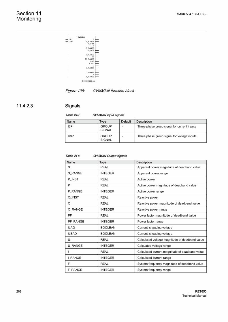
CVMMXNI3P*U3P*
SS_RANGE
P_INSTP
P_RANGEQ_INST
QQ_RANGE
PFPF_RANGE
ILAGILEAD
UU_RANGE
II_RANGE
FF_RANGE
IEC08000222.vsd
IEC08000222 V1 EN
Figure 108: CVMMXN function block
11.4.2.3 Signals
Table 240: CVMMXN Input signals
Name Type Default DescriptionI3P GROUP
SIGNAL- Three phase group signal for current inputs
U3P GROUPSIGNAL
- Three phase group signal for voltage inputs
Table 241: CVMMXN Output signals
Name Type DescriptionS REAL Apparent power magnitude of deadband value
S_RANGE INTEGER Apparent power range
P_INST REAL Active power
P REAL Active power magnitude of deadband value
P_RANGE INTEGER Active power range
Q_INST REAL Reactive power
Q REAL Reactive power magnitude of deadband value
Q_RANGE INTEGER Reactive power range
PF REAL Power factor magnitude of deadband value
PF_RANGE INTEGER Power factor range
ILAG BOOLEAN Current is lagging voltage
ILEAD BOOLEAN Current is leading voltage
U REAL Calculated voltage magnitude of deadband value
U_RANGE INTEGER Calcuated voltage range
I REAL Calculated current magnitude of deadband value
I_RANGE INTEGER Calculated current range
F REAL System frequency magnitude of deadband value
F_RANGE INTEGER System frequency range
Section 11 1MRK 504 106-UEN -Monitoring
268 RET650Technical Manual

11.4.2.4 Settings
Table 242: CVMMXN Non group settings (basic)
Name Values (Range) Unit Step Default DescriptionOperation Off
On- - Off Operation Off / On
GlobalBaseSel 1 - 6 - 1 1 Selection of one of the Global BaseValue groups
Mode L1, L2, L3AronePos SeqL1L2L2L3L3L1L1L2L3
- - L1, L2, L3 Selection of measured current andvoltage
PowAmpFact 0.000 - 6.000 - 0.001 1.000 Amplitude factor to scale powercalculations
PowAngComp -180.0 - 180.0 Deg 0.1 0.0 Angle compensation for phase shiftbetween measured I & U
k 0.00 - 1.00 - 0.01 0.00 Low pass filter coefficient for powermeasurement
SLowLim 0.0 - 2000.0 %SB 0.1 80.0 Low limit in % of SBase
SLowLowLim 0.0 - 2000.0 %SB 0.1 60.0 Low Low limit in % of SBase
SMin 0.0 - 2000.0 %SB 0.1 50.0 Minimum value in % of SBase
SMax 0.0 - 2000.0 %SB 0.1 200.0 Maximum value in % of SBase
SRepTyp CyclicDead bandInt deadband
- - Cyclic Reporting type
PMin -2000.0 - 2000.0 %SB 0.1 -200.0 Minimum value in % of SBase
PMax -2000.0 - 2000.0 %SB 0.1 200.0 Maximum value in % of SBase
PRepTyp CyclicDead bandInt deadband
- - Cyclic Reporting type
QMin -2000.0 - 2000.0 %SB 0.1 -200.0 Minimum value in % of SBase
QMax -2000.0 - 2000.0 %SB 0.1 200.0 Maximum value in % of SBase
QRepTyp CyclicDead bandInt deadband
- - Cyclic Reporting type
PFMin -1.000 - 1.000 - 0.001 -1.000 Minimum value
PFMax -1.000 - 1.000 - 0.001 1.000 Maximum value
PFRepTyp CyclicDead bandInt deadband
- - Cyclic Reporting type
UMin 0.0 - 200.0 %UB 0.1 50.0 Minimum value in % of UBase
UMax 0.0 - 200.0 %UB 0.1 200.0 Maximum value in % of UBase
URepTyp CyclicDead bandInt deadband
- - Cyclic Reporting type
Table continues on next page
1MRK 504 106-UEN - Section 11Monitoring
RET650 269Technical Manual

Name Values (Range) Unit Step Default DescriptionIMin 0.0 - 500.0 %IB 0.1 50.0 Minimum value in % of IBase
IMax 0.0 - 500.0 %IB 0.1 200.0 Maximum value in % of IBase
IRepTyp CyclicDead bandInt deadband
- - Cyclic Reporting type
FrMin 0.000 - 100.000 Hz 0.001 0.000 Minimum value
FrMax 0.000 - 100.000 Hz 0.001 70.000 Maximum value
FrRepTyp CyclicDead bandInt deadband
- - Cyclic Reporting type
Table 243: CVMMXN Non group settings (advanced)
Name Values (Range) Unit Step Default DescriptionSDbRepInt 1 - 300 Type 1 10 Cycl: Report interval (s), Db: In % of
range, Int Db: In %s
SZeroDb 0 - 100000 m% 1 500 Zero point clamping in 0,001% of range
SHiHiLim 0.0 - 2000.0 %SB 0.1 150.0 High High limit in % of SBase
SHiLim 0.0 - 2000.0 %SB 0.1 120.0 High limit in % of SBase
PHiHiLim -2000.0 - 2000.0 %SB 0.1 150.0 High High limit in % of SBase
SLimHyst 0.000 - 100.000 % 0.001 5.000 Hysteresis value in % of range (commonfor all limits)
PDbRepInt 1 - 300 Type 1 10 Cycl: Report interval (s), Db: In % ofrange, Int Db: In %s
PZeroDb 0 - 100000 m% 1 500 Zero point clamping
PHiLim -2000.0 - 2000.0 %SB 0.1 120.0 High limit in % of SBase
PLowLim -2000.0 - 2000.0 %SB 0.1 -120.0 Low limit in % of SBase
PLowLowLim -2000.0 - 2000.0 %SB 0.1 -150.0 Low Low limit in % of SBase
PLimHyst 0.000 - 100.000 % 0.001 5.000 Hysteresis value in % of range (commonfor all limits)
QDbRepInt 1 - 300 Type 1 10 Cycl: Report interval (s), Db: In % ofrange, Int Db: In %s
QZeroDb 0 - 100000 m% 1 500 Zero point clamping
QHiHiLim -2000.0 - 2000.0 %SB 0.1 150.0 High High limit in % of SBase
QHiLim -2000.0 - 2000.0 %SB 0.1 120.0 High limit in % of SBase
QLowLim -2000.0 - 2000.0 %SB 0.1 -120.0 Low limit in % of SBase
QLowLowLim -2000.0 - 2000.0 %SB 0.1 -150.0 Low Low limit in % of SBase
QLimHyst 0.000 - 100.000 % 0.001 5.000 Hysteresis value in % of range (commonfor all limits)
PFDbRepInt 1 - 300 Type 1 10 Cycl: Report interval (s), Db: In % ofrange, Int Db: In %s
PFZeroDb 0 - 100000 m% 1 500 Zero point clamping
PFHiHiLim -1.000 - 1.000 - 0.001 1.000 High High limit (physical value)
PFHiLim -1.000 - 1.000 - 0.001 0.800 High limit (physical value)
Table continues on next page
Section 11 1MRK 504 106-UEN -Monitoring
270 RET650Technical Manual

Name Values (Range) Unit Step Default DescriptionPFLowLim -1.000 - 1.000 - 0.001 -0.800 Low limit (physical value)
PFLowLowLim -1.000 - 1.000 - 0.001 -1.000 Low Low limit (physical value)
PFLimHyst 0.000 - 100.000 % 0.001 5.000 Hysteresis value in % of range (commonfor all limits)
UDbRepInt 1 - 300 Type 1 10 Cycl: Report interval (s), Db: In % ofrange, Int Db: In %s
UZeroDb 0 - 100000 m% 1 500 Zero point clamping
UHiHiLim 0.0 - 200.0 %UB 0.1 150.0 High High limit in % of UBase
UHiLim 0.0 - 200.0 %UB 0.1 120.0 High limit in % of UBase
ULowLim 0.0 - 200.0 %UB 0.1 80.0 Low limit in % of UBase
ULowLowLim 0.0 - 200.0 %UB 0.1 60.0 Low Low limit in % of UBase
ULimHyst 0.000 - 100.000 % 0.001 5.000 Hysteresis value in % of range (commonfor all limits)
IDbRepInt 1 - 300 Type 1 10 Cycl: Report interval (s), Db: In % ofrange, Int Db: In %s
IZeroDb 0 - 100000 m% 1 500 Zero point clamping
IHiHiLim 0.0 - 500.0 %IB 0.1 150.0 High High limit in % of IBase
IHiLim 0.0 - 500.0 %IB 0.1 120.0 High limit in % of IBase
ILowLim 0.0 - 500.0 %IB 0.1 80.0 Low limit in % of IBase
ILowLowLim 0.0 - 500.0 %IB 0.1 60.0 Low Low limit in % of IBase
ILimHyst 0.000 - 100.000 % 0.001 5.000 Hysteresis value in % of range (commonfor all limits)
FrDbRepInt 1 - 300 Type 1 10 Cycl: Report interval (s), Db: In % ofrange, Int Db: In %s
FrZeroDb 0 - 100000 m% 1 500 Zero point clamping
FrHiHiLim 0.000 - 100.000 Hz 0.001 65.000 High High limit (physical value)
FrHiLim 0.000 - 100.000 Hz 0.001 63.000 High limit (physical value)
FrLowLim 0.000 - 100.000 Hz 0.001 47.000 Low limit (physical value)
FrLowLowLim 0.000 - 100.000 Hz 0.001 45.000 Low Low limit (physical value)
FrLimHyst 0.000 - 100.000 % 0.001 5.000 Hysteresis value in % of range (commonfor all limits)
UAmpComp5 -10.000 - 10.000 % 0.001 0.000 Amplitude factor to calibrate voltage at5% of Ur
UAmpComp30 -10.000 - 10.000 % 0.001 0.000 Amplitude factor to calibrate voltage at30% of Ur
UAmpComp100 -10.000 - 10.000 % 0.001 0.000 Amplitude factor to calibrate voltage at100% of Ur
IAmpComp5 -10.000 - 10.000 % 0.001 0.000 Amplitude factor to calibrate current at5% of Ir
IAmpComp30 -10.000 - 10.000 % 0.001 0.000 Amplitude factor to calibrate current at30% of Ir
IAmpComp100 -10.000 - 10.000 % 0.001 0.000 Amplitude factor to calibrate current at100% of Ir
Table continues on next page
1MRK 504 106-UEN - Section 11Monitoring
RET650 271Technical Manual

Name Values (Range) Unit Step Default DescriptionIAngComp5 -10.000 - 10.000 Deg 0.001 0.000 Angle calibration for current at 5% of Ir
IAngComp30 -10.000 - 10.000 Deg 0.001 0.000 Angle calibration for current at 30% of Ir
IAngComp100 -10.000 - 10.000 Deg 0.001 0.000 Angle calibration for current at 100% of Ir
11.4.2.5 Monitored data
Table 244: CVMMXN Monitored data
Name Type Values (Range) Unit DescriptionS REAL - MVA Apparent power
magnitude of deadbandvalue
P REAL - MW Active power magnitudeof deadband value
Q REAL - MVAr Reactive powermagnitude of deadbandvalue
PF REAL - - Power factor magnitudeof deadband value
U REAL - kV Calculated voltagemagnitude of deadbandvalue
I REAL - A Calculated currentmagnitude of deadbandvalue
F REAL - Hz System frequencymagnitude of deadbandvalue
11.4.3 Phase current measurement CMMXU
11.4.3.1 Identification
Function description IEC 61850identification
IEC 60617identification
ANSI/IEEE C37.2device number
Phase current measurement CMMXU
I
SYMBOL-SS V1 EN
-
11.4.3.2 Function block
The available function blocks of an IED are depending on the actual hardware(TRM) and the logic configuration made in PCM600.
Section 11 1MRK 504 106-UEN -Monitoring
272 RET650Technical Manual

CMMXUI3P IL1
IL1RANGIL1ANGL
IL2IL2RANGIL2ANGL
IL3IL3RANGIL3ANGL
IEC08000225 V1 EN
Figure 109: CMMXU function block
11.4.3.3 Signals
Table 245: CMMXU Input signals
Name Type Default DescriptionI3P GROUP
SIGNAL- Three phase group signal for current inputs
Table 246: CMMXU Output signals
Name Type DescriptionIL1 REAL IL1 Amplitude
IL1RANG INTEGER IL1 Amplitude range
IL1ANGL REAL IL1 Angle
IL2 REAL IL2 Amplitude
IL2RANG INTEGER IL2 Amplitude range
IL2ANGL REAL IL2 Angle
IL3 REAL IL3 Amplitude
IL3RANG INTEGER IL3 Amplitude range
IL3ANGL REAL IL3 Angle
11.4.3.4 Settings
Table 247: CMMXU Non group settings (basic)
Name Values (Range) Unit Step Default DescriptionOperation Off
On- - Off Operation Off / On
GlobalBaseSel 1 - 6 - 1 1 Global Base Selector
ILDbRepInt 1 - 300 s,%,%s 1 10 Cycl: Report interval (s), Db: In % ofrange, Int Db: In %s
ILMax 0 - 500000 A 1 1300 Maximum value
ILRepTyp CyclicDead bandInt deadband
- - Dead band Reporting type
ILAngDbRepInt 1 - 300 s,%,%s 1 10 Cycl: Report interval (s), Db: In % ofrange, Int Db: In %s
1MRK 504 106-UEN - Section 11Monitoring
RET650 273Technical Manual

Table 248: CMMXU Non group settings (advanced)
Name Values (Range) Unit Step Default DescriptionILZeroDb 0 - 100000 1/1000% 1 500 Zero point clamping
ILHiHiLim 0 - 500000 A 1 1200 High High limit (physical value)
ILHiLim 0 - 500000 A 1 1100 High limit (physical value)
ILLowLim 0 - 500000 A 1 0 Low limit (physical value)
ILLowLowLim 0 - 500000 A 1 00 Low Low limit (physical value)
ILMin 0 - 500000 A 1 0 Minimum value
ILLimHys 0.000 - 100.000 % 0.001 5.000 Hysteresis value in % of range and iscommon for all limits
IAmpComp5 -10.000 - 10.000 % 0.001 0.000 Amplitude factor to calibrate current at5% of Ir
IAmpComp30 -10.000 - 10.000 % 0.001 0.000 Amplitude factor to calibrate current at30% of Ir
IAmpComp100 -10.000 - 10.000 % 0.001 0.000 Amplitude factor to calibrate current at100% of Ir
IAngComp5 -10.000 - 10.000 Deg 0.001 0.000 Angle calibration for current at 5% of Ir
IAngComp30 -10.000 - 10.000 Deg 0.001 0.000 Angle calibration for current at 30% of Ir
IAngComp100 -10.000 - 10.000 Deg 0.001 0.000 Angle calibration for current at 100% of Ir
11.4.3.5 Monitored data
Table 249: CMMXU Monitored data
Name Type Values (Range) Unit DescriptionIL1 REAL - A IL1 Amplitude
IL1ANGL REAL - deg IL1 Angle
IL2 REAL - A IL2 Amplitude
IL2ANGL REAL - deg IL2 Angle
IL3 REAL - A IL3 Amplitude
IL3ANGL REAL - deg IL3 Angle
11.4.4 Phase-phase voltage measurement VMMXU
11.4.4.1 Identification
Function description IEC 61850identification
IEC 60617identification
ANSI/IEEE C37.2device number
Phase-phase voltage measurement VMMXU
U
SYMBOL-UU V1 EN
-
Section 11 1MRK 504 106-UEN -Monitoring
274 RET650Technical Manual

11.4.4.2 Function block
The available function blocks of an IED are depending on the actual hardware(TRM) and the logic configuration made in PCM600.
VMMXUU3P UL12
UL12RANGUL12ANGL
UL23UL23RANGUL23ANGL
UL31UL31RANGUL31ANGL
IEC08000223 V1 EN
Figure 110: VMMXU function block
11.4.4.3 Signals
Table 250: VMMXU Input signals
Name Type Default DescriptionU3P GROUP
SIGNAL- Three phase group signal for voltage inputs
Table 251: VMMXU Output signals
Name Type DescriptionUL12 REAL UL12 Amplitude
UL12RANG INTEGER UL12 Amplitude range
UL12ANGL REAL UL12 Angle
UL23 REAL UL23 Amplitude
UL23RANG INTEGER UL23 Amplitude range
UL23ANGL REAL UL23 Angle
UL31 REAL UL31 Amplitude
UL31RANG INTEGER UL31Amplitude range
UL31ANGL REAL UL31 Angle
11.4.4.4 Settings
Table 252: VMMXU Non group settings (basic)
Name Values (Range) Unit Step Default DescriptionOperation Off
On- - Off Operation Off / On
GlobalBaseSel 1 - 6 - 1 1 Global Base Selector
ULDbRepInt 1 - 300 s,%,%s 1 10 Cycl: Report interval (s), Db: In % ofrange, Int Db: In %s
Table continues on next page
1MRK 504 106-UEN - Section 11Monitoring
RET650 275Technical Manual

Name Values (Range) Unit Step Default DescriptionULMax 0 - 4000000 V 1 170000 Maximum value
ULRepTyp CyclicDead bandInt deadband
- - Dead band Reporting type
ULAngDbRepInt 1 - 300 s,%,%s 1 10 Cycl: Report interval (s), Db: In % ofrange, Int Db: In %s
Table 253: VMMXU Non group settings (advanced)
Name Values (Range) Unit Step Default DescriptionULZeroDb 0 - 100000 1/1000% 1 500 Zero point clamping
ULHiHiLim 0 - 4000000 V 1 160000 High High limit (physical value)
ULHiLim 0 - 4000000 V 1 150000 High limit (physical value)
ULLowLim 0 - 4000000 V 1 125000 Low limit (physical value)
ULLowLowLim 0 - 4000000 V 1 115000 Low Low limit (physical value)
ULMin 0 - 4000000 V 1 0 Minimum value
ULLimHys 0.000 - 100.000 V 0.001 5.0000 Hysteresis value in % of range and iscommon for all limits
11.4.4.5 Monitored data
Table 254: VMMXU Monitored data
Name Type Values (Range) Unit DescriptionUL12 REAL - kV UL12 Amplitude
UL12ANGL REAL - deg UL12 Angle
UL23 REAL - kV UL23 Amplitude
UL23ANGL REAL - deg UL23 Angle
UL31 REAL - kV UL31 Amplitude
UL31ANGL REAL - deg UL31 Angle
11.4.5 Current sequence component measurement CMSQI
11.4.5.1 Identification
Function description IEC 61850identification
IEC 60617identification
ANSI/IEEE C37.2device number
Current sequence componentmeasurement
CMSQI
I1, I2, I0
SYMBOL-VV V1 EN
-
Section 11 1MRK 504 106-UEN -Monitoring
276 RET650Technical Manual

11.4.5.2 Function block
The available function blocks of an IED are depending on the actual hardware(TRM) and the logic configuration made in PCM600.
CMSQII3P 3I0
3I0RANG3I0ANGL
I1I1RANGI1ANGL
I2I2RANGI2ANGL
IEC08000221 V1 EN
Figure 111: CMSQI function block
11.4.5.3 Signals
Table 255: CMSQI Input signals
Name Type Default DescriptionI3P GROUP
SIGNAL- Three phase group signal for current inputs
Table 256: CMSQI Output signals
Name Type Description3I0 REAL 3I0 Amplitude
3I0RANG INTEGER 3I0 Amplitude range
3I0ANGL REAL 3I0 Angle
I1 REAL I1 Amplitude
I1RANG INTEGER I1Amplitude range
I1ANGL REAL I1 Angle
I2 REAL I2 Amplitude
I2RANG INTEGER I2 Amplitude range
I2ANGL REAL I2Angle
11.4.5.4 Settings
Table 257: CMSQI Non group settings (basic)
Name Values (Range) Unit Step Default DescriptionOperation Off
On- - Off Operation Off / On
3I0DbRepInt 1 - 300 s,%,%s 1 10 Cycl: Report interval (s), Db: In % ofrange, Int Db: In %s
3I0Min 0 - 500000 A 1 0 Minimum value
3I0Max 0 - 500000 A 1 3300 Maximum value
Table continues on next page
1MRK 504 106-UEN - Section 11Monitoring
RET650 277Technical Manual

Name Values (Range) Unit Step Default Description3I0RepTyp Cyclic
Dead bandInt deadband
- - Dead band Reporting type
3I0LimHys 0.000 - 100.000 % 0.001 5.000 Hysteresis value in % of range and iscommon for all limits
3I0AngDbRepInt 1 - 300 s,%,%s 1 10 Cycl: Report interval (s), Db: In % ofrange, Int Db: In %s
I1DbRepInt 1 - 300 s,%,%s 1 10 Cycl: Report interval (s), Db: In % ofrange, Int Db: In %s
I1Min 0 - 500000 A 1 0 Minimum value
I1Max 0 - 500000 A 1 1300 Maximum value
I1RepTyp CyclicDead bandInt deadband
- - Dead band Reporting type
I1AngDbRepInt 1 - 300 s,%,%s 1 10 Cycl: Report interval (s), Db: In % ofrange, Int Db: In %s
I2DbRepInt 1 - 300 s,%,%s 1 10 Cycl: Report interval (s), Db: In % ofrange, Int Db: In %s
I2Min 0 - 500000 A 1 0 Minimum value
I2Max 0 - 500000 A 1 1300 Maximum value
I2RepTyp CyclicDead bandInt deadband
- - Dead band Reporting type
I2LimHys 0.000 - 100.000 % 0.001 5.000 Hysteresis value in % of range and iscommon for all limits
I2AngDbRepInt 1 - 300 s,%,%s 1 10 Cycl: Report interval (s), Db: In % ofrange, Int Db: In %s
Table 258: CMSQI Non group settings (advanced)
Name Values (Range) Unit Step Default Description3I0ZeroDb 0 - 100000 1/1000% 1 500 Zero point clamping
3I0HiHiLim 0 - 500000 A 1 3600 High High limit (physical value)
3I0HiLim 0 - 500000 A 1 3300 High limit (physical value)
3I0LowLim 0 - 500000 A 1 0 Low limit (physical value)
3I0LowLowLim 0 - 500000 A 1 0 Low Low limit (physical value)
I1ZeroDb 0 - 100000 1/1000% 1 500 Zero point clamping
I1HiHiLim 0 - 500000 A 1 1200 High High limit (physical value)
I1HiLim 0 - 500000 A 1 1100 High limit (physical value)
I1LowLim 0 - 500000 A 1 0 Low limit (physical value)
I1LowLowLim 0 - 500000 A 1 0 Low Low limit (physical value)
I1LimHys 0.000 - 100.000 % 0.001 5.000 Hysteresis value in % of range and iscommon for all limits
I2ZeroDb 0 - 100000 1/1000% 1 500 Zero point clamping
I2HiHiLim 0 - 500000 A 1 1200 High High limit (physical value)
Table continues on next page
Section 11 1MRK 504 106-UEN -Monitoring
278 RET650Technical Manual

Name Values (Range) Unit Step Default DescriptionI2HiLim 0 - 500000 A 1 1100 High limit (physical value)
I2LowLim 0 - 500000 A 1 0 Low limit (physical value)
I2LowLowLim 0 - 500000 A 1 0 Low Low limit (physical value)
11.4.5.5 Monitored data
Table 259: CMSQI Monitored data
Name Type Values (Range) Unit Description3I0 REAL - A 3I0 Amplitude
3I0ANGL REAL - deg 3I0 Angle
I1 REAL - A I1 Amplitude
I1ANGL REAL - deg I1 Angle
I2 REAL - A I2 Amplitude
I2ANGL REAL - deg I2Angle
11.4.6 Voltage sequence measurement VMSQI
11.4.6.1 Identification
Function description IEC 61850identification
IEC 60617identification
ANSI/IEEE C37.2device number
Voltage sequence measurement VMSQI
U1, U2, U0
SYMBOL-TT V1 EN
-
11.4.6.2 Function block
The available function blocks of an IED are depending on the actual hardware(TRM) and the logic configuration made in PCM600.
VMSQIU3P 3U0
3U0RANG3U0ANGL
U1U1RANGU1ANGL
U2U2RANGU2ANGL
IEC08000224 V1 EN
Figure 112: VMSQI function block
1MRK 504 106-UEN - Section 11Monitoring
RET650 279Technical Manual

11.4.6.3 Signals
Table 260: VMSQI Input signals
Name Type Default DescriptionU3P GROUP
SIGNAL- Three phase group signal for voltage inputs
Table 261: VMSQI Output signals
Name Type Description3U0 REAL 3U0 Amplitude
3U0RANG INTEGER 3U0 Amplitude range
3U0ANGL REAL 3U0 Angle
U1 REAL U1 Amplitude
U1RANG INTEGER U1 Amplitude range
U1ANGL REAL U1 Angle
U2 REAL U2 Amplitude
U2RANG INTEGER U2 Amplitude range
U2ANGL REAL U2 Angle
11.4.6.4 Settings
Table 262: VMSQI Non group settings (basic)
Name Values (Range) Unit Step Default DescriptionOperation Off
On- - Off Operation Off / On
3U0DbRepInt 1 - 300 s,%,%s 1 10 Cycl: Report interval (s), Db: In % ofrange, Int Db: In %s
3U0Min 0 - 2000000 V 1 0 Minimum value
3U0Max 0 - 2000000 V 1 318000 Maximum value
3U0RepTyp CyclicDead bandInt deadband
- - Dead band Reporting type
3U0LimHys 0.000 - 100.000 % 0.001 5.000 Hysteresis value in % of range and iscommon for all limits
3U0AngDbRepInt 1 - 300 s,%,%s 1 10 Cycl: Report interval (s), Db: In % ofrange, Int Db: In %s
U1DbRepInt 1 - 300 s,%,%s 1 10 Cycl: Report interval (s), Db: In % ofrange, Int Db: In %s
U1Min 0 - 2000000 V 1 0 Minimum value
U1Max 0 - 2000000 V 1 106000 Maximum value
U1RepTyp CyclicDead bandInt deadband
- - Dead band Reporting type
Table continues on next page
Section 11 1MRK 504 106-UEN -Monitoring
280 RET650Technical Manual

Name Values (Range) Unit Step Default DescriptionU1AngDbRepInt 1 - 300 s,%,%s 1 10 Cycl: Report interval (s), Db: In % of
range, Int Db: In %s
U2DbRepInt 1 - 300 s,%,%s 1 10 Cycl: Report interval (s), Db: In % ofrange, Int Db: In %s
U2Min 0 - 2000000 V 1 0 Minimum value
U2Max 0 - 2000000 V 1 106000 Maximum value
U2RepTyp CyclicDead bandInt deadband
- - Dead band Reporting type
U2LimHys 0.000 - 100.000 % 0.001 5.000 Hysteresis value in % of range and iscommon for all limits
U2AngDbRepInt 1 - 300 s,%,%s 1 10 Cycl: Report interval (s), Db: In % ofrange, Int Db: In %s
Table 263: VMSQI Non group settings (advanced)
Name Values (Range) Unit Step Default Description3U0ZeroDb 0 - 100000 1/1000% 1 500 Zero point clamping
3U0HiHiLim 0 - 2000000 V 1 288000 High High limit (physical value)
3U0HiLim 0 - 2000000 V 1 258000 High limit (physical value)
3U0LowLim 0 - 2000000 V 1 213000 Low limit (physical value)
3U0LowLowLim 0 - 2000000 V 1 198000 Low Low limit (physical value)
U1ZeroDb 0 - 100000 1/1000% 1 500 Zero point clamping
U1HiHiLim 0 - 2000000 V 1 96000 High High limit (physical value)
U1HiLim 0 - 2000000 V 1 86000 High limit (physical value)
U1LowLim 0 - 2000000 V 1 71000 Low limit (physical value)
U1LowLowLim 0 - 2000000 V 1 66000 Low Low limit (physical value)
U1LimHys 0.000 - 100.000 % 0.001 5.000 Hysteresis value in % of range and iscommon for all limits
U2ZeroDb 0 - 100000 1/1000% 1 500 Zero point clamping
U2HiHiLim 0 - 2000000 V 1 96000 High High limit (physical value)
U2HiLim 0 - 2000000 V 1 86000 High limit (physical value)
U2LowLim 0 - 2000000 V 1 71000 Low limit (physical value)
U2LowLowLim 0 - 2000000 V 1 66000 Low Low limit (physical value)
11.4.6.5 Monitored data
Table 264: VMSQI Monitored data
Name Type Values (Range) Unit Description3U0 REAL - kV 3U0 Amplitude
3U0ANGL REAL - deg 3U0 Angle
U1 REAL - kV U1 Amplitude
Table continues on next page
1MRK 504 106-UEN - Section 11Monitoring
RET650 281Technical Manual

Name Type Values (Range) Unit DescriptionU1ANGL REAL - deg U1 Angle
U2 REAL - kV U2 Amplitude
U2ANGL REAL - deg U2 Angle
11.4.7 Phase-neutral voltage measurement VNMMXU
11.4.7.1 Identification
Function description IEC 61850identification
IEC 60617identification
ANSI/IEEE C37.2device number
Phase-neutral voltage measurement VNMMXU
U
SYMBOL-UU V1 EN
-
11.4.7.2 Function block
The available function blocks of an IED are depending on the actual hardware(TRM) and the logic configuration made in PCM600.
VNMMXUU3P UL1
UL1RANGUL1ANGL
UL2UL2RANGUL2ANGL
UL3UL3RANGUL3ANGL
IEC08000226 V1 EN
Figure 113: VNMMXU function block
11.4.7.3 Signals
Table 265: VNMMXU Input signals
Name Type Default DescriptionU3P GROUP
SIGNAL- Three phase group signal for voltage inputs
Table 266: VNMMXU Output signals
Name Type DescriptionUL1 REAL UL1 Amplitude, magnitude of reported value
UL1RANG INTEGER UL1 Amplitude range
UL1ANGL REAL UL1 Angle, magnitude of reported value
Table continues on next page
Section 11 1MRK 504 106-UEN -Monitoring
282 RET650Technical Manual

Name Type DescriptionUL2 REAL UL2 Amplitude, magnitude of reported value
UL2RANG INTEGER UL2 Amplitude range
UL2ANGL REAL UL2 Angle, magnitude of reported value
UL3 REAL UL3 Amplitude, magnitude of reported value
UL3RANG INTEGER UL3 Amplitude range
UL3ANGL REAL UL3 Angle, magnitude of reported value
11.4.7.4 Settings
Table 267: VNMMXU Non group settings (basic)
Name Values (Range) Unit Step Default DescriptionOperation Off
On- - Off Operation Mode On / Off
GlobalBaseSel 1 - 6 - 1 1 Global Base Selector
UDbRepInt 1 - 300 s,%,%s 1 10 Cycl: Report interval (s), Db: In % ofrange, Int Db: In %s
UMax 0 - 2000000 V 1 106000 Maximum value
URepTyp CyclicDead bandInt deadband
- - Dead band Reporting type
ULimHys 0.000 - 100.000 V 0.001 5.0000 Hysteresis value in % of range and iscommon for all limits
UAngDbRepInt 1 - 300 s,%,%s 1 10 Cycl: Report interval (s), Db: In % ofrange, Int Db: In %s
Table 268: VNMMXU Non group settings (advanced)
Name Values (Range) Unit Step Default DescriptionUZeroDb 0 - 100000 1/1000% 1 500 Zero point clamping in 0,001% of range
UHiHiLim 0 - 2000000 V 1 96000 High High limit (physical value)
UHiLim 0 - 2000000 V 1 86000 High limit (physical value)
ULowLim 0 - 2000000 V 1 71000 Low limit (physical value)
ULowLowLim 0 - 2000000 V 1 66000 Low Low limit (physical value)
UMin 0 - 2000000 V 1 0 Minimum value
1MRK 504 106-UEN - Section 11Monitoring
RET650 283Technical Manual

11.4.7.5 Monitored data
Table 269: VNMMXU Monitored data
Name Type Values (Range) Unit DescriptionUL1 REAL - kV UL1 Amplitude,
magnitude of reportedvalue
UL1ANGL REAL - deg UL1 Angle, magnitude ofreported value
UL2 REAL - kV UL2 Amplitude,magnitude of reportedvalue
UL2ANGL REAL - deg UL2 Angle, magnitude ofreported value
UL3 REAL - kV UL3 Amplitude,magnitude of reportedvalue
UL3ANGL REAL - deg UL3 Angle, magnitude ofreported value
11.4.8 Operation principle
11.4.8.1 Measurement supervision
The protection, control, and monitoring IEDs have functionality to measure andfurther process information for currents and voltages obtained from the pre-processing blocks. The number of processed alternate measuring quantitiesdepends on the type of IED and built-in options.
The information on measured quantities is available for the user at different locations:
• Locally by means of the local HMI• Remotely using the monitoring tool within PCM600 or over the station bus• Internally by connecting the analogue output signals to the Disturbance Report
function
Phase angle referenceAll phase angles are presented in relation to a defined reference channel. TheGeneral setting parameter PhaseAngleRef defines the reference. ThePhaseAngleRef is set in local HMI under: Configuration/Analog modules/Reference channel service values.
Zero point clampingMeasured value below zero point clamping limit is forced to zero. This allows thenoise in the input signal to be ignored. The zero point clamping limit is a generalsetting (XZeroDb where X equals S, P, Q, PF, U, I, F, IL1-3, UL1-3, UL12-31, I1,I2, 3I0, U1, U2 or 3U0). Observe that this measurement supervision zero point
Section 11 1MRK 504 106-UEN -Monitoring
284 RET650Technical Manual

clamping might be overridden by the zero point clamping used for themeasurement values within CVMMXN.
Continuous monitoring of the measured quantityUsers can continuously monitor the measured quantity available in each functionblock by means of four defined operating thresholds, see figure 114. Themonitoring has two different modes of operating:
• Overfunction, when the measured current exceeds the High limit (XHiLim) orHigh-high limit (XHiHiLim) pre-set values
• Underfunction, when the measured current decreases under the Low limit(XLowLim) or Low-low limit (XLowLowLim) pre-set values.
X_RANGE is illustrated in figure 114.
en05000657.vsd
X_RANGE= 1
X_RANGE = 3
X_RANGE=0
Hysteresis
High-high limit
High limit
Low limit
Low-low limit
X_RANGE=2
X_RANGE=4
Y
tX_RANGE=0
IEC05000657 V1 EN
Figure 114: Presentation of operating limits
Each analogue output has one corresponding supervision level output(X_RANGE). The output signal is an integer in the interval 0-4 (0: Normal, 1:High limit exceeded, 3: High-high limit exceeded, 2: below Low limit and 4: belowLow-low limit). The output may be connected to a measurement expander block(XP (RANGE_XP)) to get measurement supervision as binary signals.
The logical value of the functional output signals changes according to figure 114.
The user can set the hysteresis (XLimHyst), which determines the differencebetween the operating and reset value at each operating point, in wide range foreach measuring channel separately. The hysteresis is common for all operatingvalues within one channel.
Actual value of the measured quantityThe actual value of the measured quantity is available locally and remotely. Themeasurement is continuous for each measured quantity separately, but the reporting
1MRK 504 106-UEN - Section 11Monitoring
RET650 285Technical Manual

of the value to the higher levels depends on the selected reporting mode. Thefollowing basic reporting modes are available:
• Cyclic reporting (Cyclic)• Amplitude dead-band supervision (Dead band)• Integral dead-band supervision (Int deadband)
Cyclic reportingThe cyclic reporting of measured value is performed according to chosen setting(XRepTyp). The measuring channel reports the value independent of amplitude orintegral dead-band reporting.
In addition to the normal cyclic reporting the IED also report spontaneously whenmeasured value passes any of the defined threshold limits.
en05000500.vsd
Valu
e 1
Y
t
Valu
e 2
Valu
e 3
Valu
e 4
Value Reported(1st)
Value Reported
Valu
e 5
Value Reported
Y1
Y2
Y5
Value Reported Value Reported
Y3
Y4
(*)Set value for t: XDbRepInt
t (*) t (*) t (*) t (*)
IEC05000500 V1 EN
Figure 115: Periodic reporting
Amplitude dead-band supervisionIf a measuring value is changed, compared to the last reported value, and thechange is larger than the ±ΔY pre-defined limits that are set by user (XZeroDb),then the measuring channel reports the new value to a higher level, if this isdetected by a new measured value. This limits the information flow to a minimumnecessary. Figure 116 shows an example with the amplitude dead-bandsupervision. The picture is simplified: the process is not continuous but the valuesare evaluated with a time interval of one execution cycle from each other.
Section 11 1MRK 504 106-UEN -Monitoring
286 RET650Technical Manual

99000529.vsd
Y
t
Value Reported(1st)
Value ReportedValue Reported
Y1
Y2
Y3
DYDY
DYDY
DYDY
Value Reported
IEC99000529 V1 EN
Figure 116: Amplitude dead-band supervision reporting
After the new value is reported, the ±ΔY limits for dead-band are automatically setaround it. The new value is reported only if the measured quantity changes morethan defined by the ±ΔY set limits. Even if amplitude dead-band reporting isselected, there will be a 30 s "back-ground" cyclic reporting as well.
Integral dead-band reportingThe measured value is reported if the time integral of all changes exceeds the pre-set limit (XZeroDb), figure 117, where an example of reporting with integral dead-band supervision is shown. The picture is simplified: the process is not continuousbut the values are evaluated with a time interval of one execution cycle from eachother.
The last value reported, Y1 in figure 117 serves as a basic value for furthermeasurement. A difference is calculated between the last reported and the newlymeasured value and is multiplied by the time increment (discrete integral). Theabsolute values of these integral values are added until the pre-set value isexceeded. This occurs with the value Y2 that is reported and set as a new base forthe following measurements (as well as for the values Y3, Y4 and Y5).
The integral dead-band supervision is particularly suitable for monitoring signalswith small variations that can last for relatively long periods. Even if integral dead-band reporting is selected, there will be a 30 s "back-ground" cyclic reporting as well.
1MRK 504 106-UEN - Section 11Monitoring
RET650 287Technical Manual

99000530.vsd
Y
t
Value Reported(1st)
Y1
ValueReported
A1Y2
ValueReported
Y3
Y4
AValueReported
A2
Y5A3
A4A5 A7
A6
ValueReported
A2 >=pre-set value
A1 >=pre-set valueA >=
pre-set valueA3 + A4 + A5 + A6 + A7 >=pre-set value
IEC99000530 V1 EN
Figure 117: Reporting with integral dead-band supervision
11.4.8.2 Measurements CVMMXN
Mode of operationThe measurement function must be connected to three-phase current and three-phase voltage input in the configuration tool (group signals), but it is capable tomeasure and calculate above mentioned quantities in nine different ways dependingon the available VT inputs connected to the IED. The end user can freely select bya parameter setting, which one of the nine available measuring modes shall be usedwithin the function. Available options are summarized in the following table:
Set value forparameter“Mode”
Formula used for complex, three-phase power calculation
Formula used for voltage andcurrent magnitude calculation
Comment
1 L1, L2, L3 * * *1 1 2 2 3 3= × + × + ×L L L L L LS U I U I U I
EQUATION1385 V1 EN
1 2 3
1 2 3
( ) / 3
( ) / 3
= + +
= + +
L L L
L L L
U U U U
I I I IEQUATION1386 V1 EN
Used whenthree phase-to-earthvoltages areavailable
2 Arone* *
1 2 1 2 3 3= × - ×L L L L L LS U I U IEQUATION1387 V1 EN (Equation 55)
1 2 2 3
1 3
( ) / 2
( ) / 2
= +
= +
L L L L
L L
U U U
I I I
EQUATION1388 V1 EN (Equation 56)
Used whenthree twophase-to-phasevoltages areavailable
3 PosSeq*3= × ×PosSeq PosSeqS U I
EQUATION1389 V1 EN (Equation 57)
3= ×
=
PosSeq
PosSeq
U U
I I
EQUATION1390 V1 EN (Equation 58)
Used whenonlysymmetricalthree phasepower shallbe measured
Table continues on next page
Section 11 1MRK 504 106-UEN -Monitoring
288 RET650Technical Manual

Set value forparameter“Mode”
Formula used for complex, three-phase power calculation
Formula used for voltage andcurrent magnitude calculation
Comment
4 L1L2* *
1 2 1 2( )= × -L L L LS U I IEQUATION1391 V1 EN (Equation 59)
1 2
1 2( ) / 2
=
= +
L L
L L
U U
I I I
EQUATION1392 V1 EN (Equation 60)
Used whenonly UL1L2phase-to-phasevoltage isavailable
5 L2L3* *
2 3 2 3( )= × -L L L LS U I IEQUATION1393 V1 EN (Equation 61)
2 3
2 3( ) / 2
=
= +
L L
L L
U U
I I I
EQUATION1394 V1 EN (Equation 62)
Used whenonly UL2L3phase-to-phasevoltage isavailable
6 L3L1* *
3 1 3 1( )= × -L L L LS U I IEQUATION1395 V1 EN (Equation 63)
3 1
3 1( ) / 2
=
= +
L L
L L
U U
I I I
EQUATION1396 V1 EN (Equation 64)
Used whenonly UL3L1phase-to-phasevoltage isavailable
7 L1*
1 13= × ×L LS U IEQUATION1397 V1 EN (Equation 65)
1
1
3= ×
=
L
L
U U
I I
EQUATION1398 V1 EN (Equation 66)
Used whenonly UL1phase-to-earth voltageis available
8 L2*
2 23= × ×L LS U IEQUATION1399 V1 EN (Equation 67)
2
2
3= ×
=
L
L
U U
I I
EQUATION1400 V1 EN (Equation 68)
Used whenonly UL2phase-to-earth voltageis available
9 L3*
3 33= × ×L LS U IEQUATION1401 V1 EN (Equation 69)
3
3
3= ×
=
L
L
U U
I I
EQUATION1402 V1 EN (Equation 70)
Used whenonly UL3phase-to-earth voltageis available
* means complex conjugated value
It shall be noted that only in the first two operating modes that is, 1 & 2 themeasurement function calculates exact three-phase power. In other operatingmodes that is, from 3 to 9 it calculates the three-phase power under assumption thatthe power system is fully symmetrical. Once the complex apparent power iscalculated then the P, Q, S, & PF are calculated in accordance with the followingformulas:
Re( )=P SEQUATION1403 V1 EN (Equation 71)
1MRK 504 106-UEN - Section 11Monitoring
RET650 289Technical Manual

Im( )=Q SEQUATION1404 V1 EN (Equation 72)
2 2= = +S S P Q
EQUATION1405 V1 EN (Equation 73)
cos PPF Sj= =
EQUATION1406 V1 EN (Equation 74)
Additionally to the power factor value the two binary output signals from thefunction are provided which indicates the angular relationship between current andvoltage phasors. Binary output signal ILAG is set to one when current phasor islagging behind voltage phasor. Binary output signal ILEAD is set to one whencurrent phasor is leading the voltage phasor.
Each analogue output has a corresponding supervision level output (X_RANGE).The output signal is an integer in the interval 0-4, see section "Measurementsupervision".
Calibration of analogue inputsMeasured currents and voltages used in the CVMMXN function can be calibratedto get class 0.5 measuring accuracy. This is achieved by amplitude and anglecompensation at 5, 30 and 100% of rated current and voltage. The compensationbelow 5% and above 100% is constant and linear in between, see example infigure 118.
Section 11 1MRK 504 106-UEN -Monitoring
290 RET650Technical Manual

IEC05000652 V2 EN
Figure 118: Calibration curves
The first current and voltage phase in the group signals will be used as referenceand the amplitude and angle compensation will be used for related input signals.
Low pass filteringIn order to minimize the influence of the noise signal on the measurement it ispossible to introduce the recursive, low pass filtering of the measured values for P,Q, S, U, I and power factor. This will make slower measurement response to thestep changes in the measured quantity. Filtering is performed in accordance withthe following recursive formula:
(1 )Old CalculatedX k X k X= × + - ×EQUATION1407 V1 EN (Equation 75)
where:
X is a new measured value (that is P, Q, S, U, I or PF) to be given out from the function
XOld is the measured value given from the measurement function in previous execution cycle
XCalculated is the new calculated value in the present execution cycle
k is settable parameter by the end user which influence the filter properties
1MRK 504 106-UEN - Section 11Monitoring
RET650 291Technical Manual

Default value for parameter k is 0.00. With this value the new calculated value isimmediately given out without any filtering (that is, without any additional delay).When k is set to value bigger than 0, the filtering is enabled. Appropriate value of kshall be determined separately for every application. Some typical value for k =0.14.
Zero point clampingIn order to avoid erroneous measurements when either current or voltage signal isnot present, the amplitude level for current and voltage measurement is forced tozero. When either current or voltage measurement is forced to zero automaticallythe measured values for power (P, Q & S) and power factor are forced to zero aswell. Since the measurement supervision functionality, included in the CVMMXNfunction, is using these values the zero clamping will influence the subsequentsupervision (observe the possibility to do zero point clamping within measurementsupervision, see section "Measurement supervision").
Compensation facilityIn order to compensate for small amplitude and angular errors in the completemeasurement chain (CT error, VT error, IED input transformer errors etc.) it ispossible to perform on site calibration of the power measurement. This is achievedby setting the complex constant which is then internally used within the function tomultiply the calculated complex apparent power S. This constant is set asamplitude (setting parameter PowAmpFact, default value 1.000) and angle (settingparameter PowAngComp, default value 0.0 degrees). Default values for these twoparameters are done in such way that they do not influence internally calculatedvalue (complex constant has default value 1). In this way calibration, for specificoperating range (for example, around rated power) can be done at site. However, toperform this calibration it is necessary to have an external power meter with highaccuracy class available.
DirectionalityCTStartPoint defines if the CTs earthing point is located towards or from theprotected object under observation. If everything is properly set power is alwaysmeasured towards protection object.
Section 11 1MRK 504 106-UEN -Monitoring
292 RET650Technical Manual

Busbar
Protected Object
P Q
IEC09000038-1-en.vsd
IED
IEC09000038-1-EN V1 EN
Figure 119: Internal IED directionality convention for P & Q measurements
Practically, it means that active and reactive power will have positive values whenthey flow from the busbar towards the protected object and they will have negativevalues when they flow from the protected object towards the busbar.
In some application, for example, when power is measured on the secondary sideof the power transformer it might be desirable, from the end client point of view, tohave actually opposite directional convention for active and reactive powermeasurements. This can be easily achieved by setting parameter PowAngComp tovalue of 180.0 degrees. With such setting the active and reactive power will havepositive values when they flow from the protected object towards the busbar.
FrequencyFrequency is actually not calculated within measurement block. It is simplyobtained from the pre-processing block and then just given out from themeasurement block as an output.
11.4.8.3 Phase current measurement CMMXU
The CMMXU function must be connected to three-phase current input in theconfiguration tool to be operable. Currents handled in the function can becalibrated to get better then class 0.5 measuring accuracy for internal use, on theoutputs and IEC 61850. This is achieved by amplitude and angle compensation at
1MRK 504 106-UEN - Section 11Monitoring
RET650 293Technical Manual

5, 30 and 100% of rated current. The compensation below 5% and above 100% isconstant and linear in between, see figure 118 above.
Phase currents (amplitude and angle) are available on the outputs and eachamplitude output has a corresponding supervision level output (ILx_RANG). Thesupervision output signal is an integer in the interval 0-4, see section "Measurement supervision".
11.4.8.4 Phase-phase and phase-neutral voltage measurements VMMXU/VNMMXU
The voltage function must be connected to three-phase voltage input in theconfiguration tool to be operable. Voltages are handled in the same way as currentswhen it comes to class 0.5 calibrations, see above.
The voltages (phase or phase-phase voltage, amplitude and angle) are available onthe outputs and each amplitude output has a corresponding supervision level output(ULxy_RANG). The supervision output signal is an integer in the interval 0-4, seesection "Measurement supervision".
11.4.8.5 Voltage and current sequence measurements VMSQI/CMSQI
The measurement functions must be connected to three-phase current (CMSQI) orvoltage (VMSQI) input in the configuration tool to be operable. No outputs, butXRANG, are calculated within the measuring block and it is not possible tocalibrate the signals. Input signals are obtained from the pre-processing block andtransferred to corresponding output.
Positive, negative and three times zero sequence quantities are available on theoutputs (voltage and current, amplitude and angle). Each amplitude output has acorresponding supervision level output (X_RANGE). The output signal is aninteger in the interval 0-4, see section "Measurement supervision".
11.4.9 Technical dataTable 270: CVMMXN Tehcnical data
Function Range or value AccuracyFrequency (0.95-1.05) × fr ± 2.0 mHz
Connected current (0.2-4.0) × Ir ± 0.5% of Ir at I £ Ir± 0.5% of I at I > Ir
Section 11 1MRK 504 106-UEN -Monitoring
294 RET650Technical Manual

11.5 Event Counter CNTGGIO
11.5.1 IdentificationFunction description IEC 61850
identificationIEC 60617identification
ANSI/IEEE C37.2device number
Event counter CNTGGIOS00946 V1 EN
-
11.5.2 FunctionalityEvent counter (CNTGGIO) has six counters which are used for storing the numberof times each counter input has been activated.
11.5.3 Function blockCNTGGIO
BLOCKCOUNTER1COUNTER2COUNTER3COUNTER4COUNTER5COUNTER6RESET
VALUE1VALUE2VALUE3VALUE4VALUE5VALUE6
IEC09000090_1_en.vsd
IEC09000090 V1 EN
Figure 120: CNTGGIO function block
11.5.4 SignalsTable 271: CNTGGIO Input signals
Name Type Default DescriptionBLOCK BOOLEAN 0 Block of function
COUNTER1 BOOLEAN 0 Input for counter 1
COUNTER2 BOOLEAN 0 Input for counter 2
COUNTER3 BOOLEAN 0 Input for counter 3
COUNTER4 BOOLEAN 0 Input for counter 4
COUNTER5 BOOLEAN 0 Input for counter 5
COUNTER6 BOOLEAN 0 Input for counter 6
RESET BOOLEAN 0 Reset of function
1MRK 504 106-UEN - Section 11Monitoring
RET650 295Technical Manual

Table 272: CNTGGIO Output signals
Name Type DescriptionVALUE1 INTEGER Output of counter 1
VALUE2 INTEGER Output of counter 2
VALUE3 INTEGER Output of counter 3
VALUE4 INTEGER Output of counter 4
VALUE5 INTEGER Output of counter 5
VALUE6 INTEGER Output of counter 6
11.5.5 SettingsTable 273: CNTGGIO Group settings (basic)
Name Values (Range) Unit Step Default DescriptionOperation Off
On- - Off Operation Off / On
11.5.6 Monitored dataTable 274: CNTGGIO Monitored data
Name Type Values (Range) Unit DescriptionVALUE1 INTEGER - - Output of counter 1
VALUE2 INTEGER - - Output of counter 2
VALUE3 INTEGER - - Output of counter 3
VALUE4 INTEGER - - Output of counter 4
VALUE5 INTEGER - - Output of counter 5
VALUE6 INTEGER - - Output of counter 6
11.5.7 Operation principleEvent counter (CNTGGIO) has six counter inputs. CNTGGIO stores how manytimes each of the inputs has been activated. The counter memory for each of the sixinputs is updated, giving the total number of times the input has been activated, assoon as an input is activated. The maximum count up speed is 10 pulses persecond. The maximum counter value is 10 000. For counts above 10 000 thecounter will stop at 10 000 and no restart will take place.
To not risk that the flash memory is worn out due to too many writings, amechanism for limiting the number of writings per time period is included in theproduct. This however gives as a result that it can take long time, up to severalminutes, before a new value is stored in the flash memory. And if a newCNTGGIO value is not stored before auxiliary power interruption, it will be lost.
Section 11 1MRK 504 106-UEN -Monitoring
296 RET650Technical Manual

The CNTGGIO stored values in flash memory will however not be lost at anauxiliary power interruption.
The function block also has an input BLOCK. At activation of this input all sixcounters are blocked. The input can for example, be used for blocking the countersat testing.The function block has an input RESET. At activation of this input all sixcounters are set to 0.
All inputs are configured via PCM 600.
11.5.7.1 Reporting
The content of the counters can be read in the local HMI.
Reset of counters can be performed in the local HMI and a binary input.
Reading of content can also be performed remotely, for example from a IEC 61850client. The value can also be presented as a measuring value on the local HMIgraphical display.
11.5.8 Technical dataTable 275: CNTGGIO Technical data
Function Range or value AccuracyCounter value 0-10000 -
Max. count up speed 10 pulses/s -
11.6 Disturbance report
11.6.1 FunctionalityComplete and reliable information about disturbances in the primary and/or in thesecondary system together with continuous event-logging is accomplished by thedisturbance report functionality.
Disturbance report, always included in the IED, acquires sampled data of allselected analog input and binary signals connected to the function block that is,maximum 40 analog and 96 binary signals.
Disturbance report functionality is a common name for several functions:
• Event List• Indications• Event recorder• Trip Value recorder• Disturbance recorder
1MRK 504 106-UEN - Section 11Monitoring
RET650 297Technical Manual

Disturbance report function is characterized by great flexibility regardingconfiguration, starting conditions, recording times and large storage capacity.
A disturbance is defined as an activation of an input in the AxRADR or BxRBDRfunction blocks which is set to trigger the disturbance recorder. All signals fromstart of pre-fault time to the end of post-fault time, will be included in the recording.
Every disturbance report recording is saved in the IED in the standard Comtradeformat. The same applies to all events, which are continuously saved in a ring-buffer. The local HMI is used to get information about the recordings, but thedisturbance report files may be uploaded to PCM600 (Protection and Control IEDManager) and further analysis using the disturbance handling tool.
11.6.2 Disturbance report DRPRDRE
11.6.2.1 Identification
Function description IEC 61850identification
IEC 60617identification
ANSI/IEEE C37.2device number
Disturbance report DRPRDRE - -
11.6.2.2 Function block
DRPRDREDRPOFF
RECSTARTRECMADECLEARED
MEMUSED
IEC09000346-1-en.vsdIEC09000346 V1 EN
Figure 121: DRPRDRE function block
11.6.2.3 Signals
Table 276: DRPRDRE Output signals
Name Type DescriptionDRPOFF BOOLEAN Disturbance report function turned off
RECSTART BOOLEAN Disturbance recording started
RECMADE BOOLEAN Disturbance recording made
CLEARED BOOLEAN All disturbances in the disturbance report cleared
MEMUSED BOOLEAN More than 80% of memory used
Section 11 1MRK 504 106-UEN -Monitoring
298 RET650Technical Manual

11.6.2.4 Settings
Table 277: DRPRDRE Non group settings (basic)
Name Values (Range) Unit Step Default DescriptionOperation Off
On- - Off Operation Off/On
PreFaultRecT 0.05 - 1.00 s 0.01 0.10 Pre-fault recording time
PostFaultRecT 0.1 - 10.0 s 0.1 0.5 Post-fault recording time
TimeLimit 0.5 - 10.0 s 0.1 1.0 Fault recording time limit
PostRetrig OffOn
- - Off Post-fault retrig enabled (On) or not (Off)
MaxNoStoreRec 10 - 100 - 1 100 Maximum number of stored disturbances
ZeroAngleRef 1 - 30 Ch 1 1 Trip value recorder, phasor referencechannel
OpModeTest OffOn
- - Off Operation mode during test mode
11.6.2.5 Monitored data
Table 278: DRPRDRE Monitored data
Name Type Values (Range) Unit DescriptionMemoryUsed INTEGER - % Memory usage (0-100%)
UnTrigStatCh1 BOOLEAN - - Under level trig foranalog channel 1activated
OvTrigStatCh1 BOOLEAN - - Over level trig for analogchannel 1 activated
UnTrigStatCh2 BOOLEAN - - Under level trig foranalog channel 2activated
OvTrigStatCh2 BOOLEAN - - Over level trig for analogchannel 2 activated
UnTrigStatCh3 BOOLEAN - - Under level trig foranalog channel 3activated
OvTrigStatCh3 BOOLEAN - - Over level trig for analogchannel 3 activated
UnTrigStatCh4 BOOLEAN - - Under level trig foranalog channel 4activated
OvTrigStatCh4 BOOLEAN - - Over level trig for analogchannel 4 activated
UnTrigStatCh5 BOOLEAN - - Under level trig foranalog channel 5activated
OvTrigStatCh5 BOOLEAN - - Over level trig for analogchannel 5 activated
Table continues on next page
1MRK 504 106-UEN - Section 11Monitoring
RET650 299Technical Manual

Name Type Values (Range) Unit DescriptionUnTrigStatCh6 BOOLEAN - - Under level trig for
analog channel 6activated
OvTrigStatCh6 BOOLEAN - - Over level trig for analogchannel 6 activated
UnTrigStatCh7 BOOLEAN - - Under level trig foranalog channel 7activated
OvTrigStatCh7 BOOLEAN - - Over level trig for analogchannel 7 activated
UnTrigStatCh8 BOOLEAN - - Under level trig foranalog channel 8activated
OvTrigStatCh8 BOOLEAN - - Over level trig for analogchannel 8 activated
UnTrigStatCh9 BOOLEAN - - Under level trig foranalog channel 9activated
OvTrigStatCh9 BOOLEAN - - Over level trig for analogchannel 9 activated
UnTrigStatCh10 BOOLEAN - - Under level trig foranalog channel 10activated
OvTrigStatCh10 BOOLEAN - - Over level trig for analogchannel 10 activated
UnTrigStatCh11 BOOLEAN - - Under level trig foranalog channel 11activated
OvTrigStatCh11 BOOLEAN - - Over level trig for analogchannel 11 activated
UnTrigStatCh12 BOOLEAN - - Under level trig foranalog channel 12activated
OvTrigStatCh12 BOOLEAN - - Over level trig for analogchannel 12 activated
UnTrigStatCh13 BOOLEAN - - Under level trig foranalog channel 13activated
OvTrigStatCh13 BOOLEAN - - Over level trig for analogchannel 13 activated
UnTrigStatCh14 BOOLEAN - - Under level trig foranalog channel 14activated
OvTrigStatCh14 BOOLEAN - - Over level trig for analogchannel 14 activated
UnTrigStatCh15 BOOLEAN - - Under level trig foranalog channel 15activated
OvTrigStatCh15 BOOLEAN - - Over level trig for analogchannel 15 activated
Table continues on next page
Section 11 1MRK 504 106-UEN -Monitoring
300 RET650Technical Manual

Name Type Values (Range) Unit DescriptionUnTrigStatCh16 BOOLEAN - - Under level trig for
analog channel 16activated
OvTrigStatCh16 BOOLEAN - - Over level trig for analogchannel 16 activated
UnTrigStatCh17 BOOLEAN - - Under level trig foranalog channel 17activated
OvTrigStatCh17 BOOLEAN - - Over level trig for analogchannel 17 activated
UnTrigStatCh18 BOOLEAN - - Under level trig foranalog channel 18activated
OvTrigStatCh18 BOOLEAN - - Over level trig for analogchannel 18 activated
UnTrigStatCh19 BOOLEAN - - Under level trig foranalog channel 19activated
OvTrigStatCh19 BOOLEAN - - Over level trig for analogchannel 19 activated
UnTrigStatCh20 BOOLEAN - - Under level trig foranalog channel 20activated
OvTrigStatCh20 BOOLEAN - - Over level trig for analogchannel 20 activated
UnTrigStatCh21 BOOLEAN - - Under level trig foranalog channel 21activated
OvTrigStatCh21 BOOLEAN - - Over level trig for analogchannel 21 activated
UnTrigStatCh22 BOOLEAN - - Under level trig foranalog channel 22activated
OvTrigStatCh22 BOOLEAN - - Over level trig for analogchannel 22 activated
UnTrigStatCh23 BOOLEAN - - Under level trig foranalog channel 23activated
OvTrigStatCh23 BOOLEAN - - Over level trig for analogchannel 23 activated
UnTrigStatCh24 BOOLEAN - - Under level trig foranalog channel 24activated
OvTrigStatCh24 BOOLEAN - - Over level trig for analogchannel 24 activated
UnTrigStatCh25 BOOLEAN - - Under level trig foranalog channel 25activated
OvTrigStatCh25 BOOLEAN - - Over level trig for analogchannel 25 activated
Table continues on next page
1MRK 504 106-UEN - Section 11Monitoring
RET650 301Technical Manual

Name Type Values (Range) Unit DescriptionUnTrigStatCh26 BOOLEAN - - Under level trig for
analog channel 26activated
OvTrigStatCh26 BOOLEAN - - Over level trig for analogchannel 26 activated
UnTrigStatCh27 BOOLEAN - - Under level trig foranalog channel 27activated
OvTrigStatCh27 BOOLEAN - - Over level trig for analogchannel 27 activated
UnTrigStatCh28 BOOLEAN - - Under level trig foranalog channel 28activated
OvTrigStatCh28 BOOLEAN - - Over level trig for analogchannel 28 activated
UnTrigStatCh29 BOOLEAN - - Under level trig foranalog channel 29activated
OvTrigStatCh29 BOOLEAN - - Over level trig for analogchannel 29 activated
UnTrigStatCh30 BOOLEAN - - Under level trig foranalog channel 30activated
OvTrigStatCh30 BOOLEAN - - Over level trig for analogchannel 30 activated
UnTrigStatCh31 BOOLEAN - - Under level trig foranalog channel 31activated
OvTrigStatCh31 BOOLEAN - - Over level trig for analogchannel 31 activated
UnTrigStatCh32 BOOLEAN - - Under level trig foranalog channel 32activated
OvTrigStatCh32 BOOLEAN - - Over level trig for analogchannel 32 activated
UnTrigStatCh33 BOOLEAN - - Under level trig foranalog channel 33activated
OvTrigStatCh33 BOOLEAN - - Over level trig for analogchannel 33 activated
UnTrigStatCh34 BOOLEAN - - Under level trig foranalog channel 34activated
OvTrigStatCh34 BOOLEAN - - Over level trig for analogchannel 34 activated
UnTrigStatCh35 BOOLEAN - - Under level trig foranalog channel 35activated
OvTrigStatCh35 BOOLEAN - - Over level trig for analogchannel 35 activated
Table continues on next page
Section 11 1MRK 504 106-UEN -Monitoring
302 RET650Technical Manual

Name Type Values (Range) Unit DescriptionUnTrigStatCh36 BOOLEAN - - Under level trig for
analog channel 36activated
OvTrigStatCh36 BOOLEAN - - Over level trig for analogchannel 36 activated
UnTrigStatCh37 BOOLEAN - - Under level trig foranalog channel 37activated
OvTrigStatCh37 BOOLEAN - - Over level trig for analogchannel 37 activated
UnTrigStatCh38 BOOLEAN - - Under level trig foranalog channel 38activated
OvTrigStatCh38 BOOLEAN - - Over level trig for analogchannel 38 activated
UnTrigStatCh39 BOOLEAN - - Under level trig foranalog channel 39activated
OvTrigStatCh39 BOOLEAN - - Over level trig for analogchannel 39 activated
UnTrigStatCh40 BOOLEAN - - Under level trig foranalog channel 40activated
OvTrigStatCh40 BOOLEAN - - Over level trig for analogchannel 40 activated
FaultNumber INTEGER - - Disturbance fault number
11.6.2.6 Measured values
Table 279: DRPRDRE Measured values
Name Type Default DescriptionManTrig BOOLEAN 0 Manual trig of disturbance report
ClearDist BOOLEAN 0 Clear all disturbances
ClearProcessEv BOOLEAN 0 Clear all process events
11.6.3 Analog input signals AxRADR
11.6.3.1 Identification
Function description IEC 61850identification
IEC 60617identification
ANSI/IEEE C37.2device number
Analog input signals A1RADR - -
Analog input signals A2RADR - -
Analog input signals A3RADR - -
1MRK 504 106-UEN - Section 11Monitoring
RET650 303Technical Manual

11.6.3.2 Function block
A1RADR^GRPINPUT1^GRPINPUT2^GRPINPUT3^GRPINPUT4^GRPINPUT5^GRPINPUT6^GRPINPUT7^GRPINPUT8^GRPINPUT9^GRPINPUT10
IEC09000348-1-en.vsdIEC09000348 V1 EN
Figure 122: A1RADR function block, analog inputs, example for A1RADR,A2RADR and A3RADR
11.6.3.3 Signals
A1RADR - A3RADR Input signalsTables for input signals for A1RADR, A2RADR and A3RADR are similar exceptfor GRPINPUT number.
• A1RADR, GRPINPUT1 - GRPINPUT10• A2RADR, GRPINPUT11 - GRPINPUT20• A3RADR, GRPINPUT21 - GRPINPUT30
Table 280: A1RADR Input signals
Name Type Default DescriptionGRPINPUT1 GROUP
SIGNAL- Group signal for input 1
GRPINPUT2 GROUPSIGNAL
- Group signal for input 2
GRPINPUT3 GROUPSIGNAL
- Group signal for input 3
GRPINPUT4 GROUPSIGNAL
- Group signal for input 4
GRPINPUT5 GROUPSIGNAL
- Group signal for input 5
GRPINPUT6 GROUPSIGNAL
- Group signal for input 6
GRPINPUT7 GROUPSIGNAL
- Group signal for input 7
GRPINPUT8 GROUPSIGNAL
- Group signal for input 8
GRPINPUT9 GROUPSIGNAL
- Group signal for input 9
GRPINPUT10 GROUPSIGNAL
- Group signal for input 10
Section 11 1MRK 504 106-UEN -Monitoring
304 RET650Technical Manual

11.6.3.4 Settings
A1RADR - A3RADR SettingsSetting tables for A1RADR, A2RADR and A3RADR are similar except forchannel numbers.
• A1RADR, channel01 - channel10• A2RADR, channel11 - channel20• A3RADR, channel21 - channel30
Table 281: A1RADR Non group settings (basic)
Name Values (Range) Unit Step Default DescriptionOperation01 Off
On- - Off Operation On/Off
Operation02 OffOn
- - Off Operation On/Off
Operation03 OffOn
- - Off Operation On/Off
Operation04 OffOn
- - Off Operation On/Off
Operation05 OffOn
- - Off Operation On/Off
Operation06 OffOn
- - Off Operation On/Off
Operation07 OffOn
- - Off Operation On/Off
Operation08 OffOn
- - Off Operation On/Off
Operation09 OffOn
- - Off Operation On/Off
Operation10 OffOn
- - Off Operation On/Off
Table 282: A1RADR Non group settings (advanced)
Name Values (Range) Unit Step Default DescriptionNomValue01 0.0 - 999999.9 - 0.1 0.0 Nominal value for analog channel 1
UnderTrigOp01 OffOn
- - Off Use under level trigger for analogchannel 1 (on) or not (off)
UnderTrigLe01 0 - 200 % 1 50 Under trigger level for analog channel 1in % of signal
OverTrigOp01 OffOn
- - Off Use over level trigger for analog channel1 (on) or not (off)
OverTrigLe01 0 - 5000 % 1 200 Over trigger level for analog channel 1 in% of signal
NomValue02 0.0 - 999999.9 - 0.1 0.0 Nominal value for analog channel 2
UnderTrigOp02 OffOn
- - Off Use under level trigger for analogchannel 2 (on) or not (off)
Table continues on next page
1MRK 504 106-UEN - Section 11Monitoring
RET650 305Technical Manual

Name Values (Range) Unit Step Default DescriptionUnderTrigLe02 0 - 200 % 1 50 Under trigger level for analog channel 2
in % of signal
OverTrigOp02 OffOn
- - Off Use over level trigger for analog channel2 (on) or not (off)
OverTrigLe02 0 - 5000 % 1 200 Over trigger level for analog channel 2 in% of signal
NomValue03 0.0 - 999999.9 - 0.1 0.0 Nominal value for analog channel 3
UnderTrigOp03 OffOn
- - Off Use under level trigger for analogchannel 3 (on) or not (off)
UnderTrigLe03 0 - 200 % 1 50 Under trigger level for analog channel 3in % of signal
OverTrigOp03 OffOn
- - Off Use over level trigger for analog channel3 (on) or not (off)
OverTrigLe03 0 - 5000 % 1 200 Overtrigger level for analog channel 3 in% of signal
NomValue04 0.0 - 999999.9 - 0.1 0.0 Nominal value for analog channel 4
UnderTrigOp04 OffOn
- - Off Use under level trigger for analogchannel 4 (on) or not (off)
UnderTrigLe04 0 - 200 % 1 50 Under trigger level for analog channel 4in % of signal
OverTrigOp04 OffOn
- - Off Use over level trigger for analog channel4 (on) or not (off)
OverTrigLe04 0 - 5000 % 1 200 Over trigger level for analog channel 4 in% of signal
NomValue05 0.0 - 999999.9 - 0.1 0.0 Nominal value for analog channel 5
UnderTrigOp05 OffOn
- - Off Use under level trigger for analogchannel 5 (on) or not (off)
UnderTrigLe05 0 - 200 % 1 50 Under trigger level for analog channel 5in % of signal
OverTrigOp05 OffOn
- - Off Use over level trigger for analog channel5 (on) or not (off)
OverTrigLe05 0 - 5000 % 1 200 Over trigger level for analog channel 5 in% of signal
NomValue06 0.0 - 999999.9 - 0.1 0.0 Nominal value for analog channel 6
UnderTrigOp06 OffOn
- - Off Use under level trigger for analogchannel 6 (on) or not (off)
UnderTrigLe06 0 - 200 % 1 50 Under trigger level for analog channel 6in % of signal
OverTrigOp06 OffOn
- - Off Use over level trigger for analog channel6 (on) or not (off)
OverTrigLe06 0 - 5000 % 1 200 Over trigger level for analog channel 6 in% of signal
NomValue07 0.0 - 999999.9 - 0.1 0.0 Nominal value for analog channel 7
UnderTrigOp07 OffOn
- - Off Use under level trigger for analogchannel 7 (on) or not (off)
UnderTrigLe07 0 - 200 % 1 50 Under trigger level for analog channel 7in % of signal
Table continues on next page
Section 11 1MRK 504 106-UEN -Monitoring
306 RET650Technical Manual

Name Values (Range) Unit Step Default DescriptionOverTrigOp07 Off
On- - Off Use over level trigger for analog channel
7 (on) or not (off)
OverTrigLe07 0 - 5000 % 1 200 Over trigger level for analog channel 7 in% of signal
NomValue08 0.0 - 999999.9 - 0.1 0.0 Nominal value for analog channel 8
UnderTrigOp08 OffOn
- - Off Use under level trigger for analogchannel 8 (on) or not (off)
UnderTrigLe08 0 - 200 % 1 50 Under trigger level for analog channel 8in % of signal
OverTrigOp08 OffOn
- - Off Use over level trigger for analog channel8 (on) or not (off)
OverTrigLe08 0 - 5000 % 1 200 Over trigger level for analog channel 8 in% of signal
NomValue09 0.0 - 999999.9 - 0.1 0.0 Nominal value for analog channel 9
UnderTrigOp09 OffOn
- - Off Use under level trigger for analogchannel 9 (on) or not (off)
UnderTrigLe09 0 - 200 % 1 50 Under trigger level for analog channel 9in % of signal
OverTrigOp09 OffOn
- - Off Use over level trigger for analog channel9 (on) or not (off)
OverTrigLe09 0 - 5000 % 1 200 Over trigger level for analog channel 9 in% of signal
NomValue10 0.0 - 999999.9 - 0.1 0.0 Nominal value for analog channel 10
UnderTrigOp10 OffOn
- - Off Use under level trigger for analogchannel 10 (on) or not (off)
UnderTrigLe10 0 - 200 % 1 50 Under trigger level for analog channel 10in % of signal
OverTrigOp10 OffOn
- - Off Use over level trigger for analog channel10 (on) or not (off)
OverTrigLe10 0 - 5000 % 1 200 Over trigger level for analog channel 10in % of signal
11.6.4 Analog input signals A4RADR
11.6.4.1 Identification
Function description IEC 61850identification
IEC 60617identification
ANSI/IEEE C37.2device number
Analog input signals A41RADR - -
1MRK 504 106-UEN - Section 11Monitoring
RET650 307Technical Manual

11.6.4.2 Function block
A4RADR^INPUT31^INPUT32^INPUT33^INPUT34^INPUT35^INPUT36^INPUT37^INPUT38^INPUT39^INPUT40
IEC09000350-1-en.vsdIEC09000350 V1 EN
Figure 123: A4RADR function block, derived analog inputs
11.6.4.3 Signals
Table 283: A4RADR Input signals
Name Type Default DescriptionINPUT31 REAL 0 Analog channel 31
INPUT32 REAL 0 Analog channel 32
INPUT33 REAL 0 Analog channel 33
INPUT34 REAL 0 Analog channel 34
INPUT35 REAL 0 Analog channel 35
INPUT36 REAL 0 Analog channel 36
INPUT37 REAL 0 Analog channel 37
INPUT38 REAL 0 Analog channel 38
INPUT39 REAL 0 Analog channel 39
INPUT40 REAL 0 Analog channel 40
11.6.4.4 Settings
Table 284: A4RADR Non group settings (basic)
Name Values (Range) Unit Step Default DescriptionOperation31 Off
On- - Off Operation On/off
Operation32 OffOn
- - Off Operation On/off
Operation33 OffOn
- - Off Operation On/off
Operation34 OffOn
- - Off Operation On/off
Operation35 OffOn
- - Off Operation On/off
Table continues on next page
Section 11 1MRK 504 106-UEN -Monitoring
308 RET650Technical Manual

Name Values (Range) Unit Step Default DescriptionOperation36 Off
On- - Off Operation On/off
Operation37 OffOn
- - Off Operation On/off
Operation38 OffOn
- - Off Operation On/off
Operation39 OffOn
- - Off Operation On/off
Operation40 OffOn
- - Off Operation On/off
Table 285: A4RADR Non group settings (advanced)
Name Values (Range) Unit Step Default DescriptionNomValue31 0.0 - 999999.9 - 0.1 0.0 Nominal value for analog channel 31
UnderTrigOp31 OffOn
- - Off Use under level trigger for analogchannel 31 (on) or not (off)
UnderTrigLe31 0 - 200 % 1 50 Under trigger level for analog channel 31in % of signal
OverTrigOp31 OffOn
- - Off Use over level trigger for analog channel31 (on) or not (off)
OverTrigLe31 0 - 5000 % 1 200 Over trigger level for analog channel 31in % of signal
NomValue32 0.0 - 999999.9 - 0.1 0.0 Nominal value for analog channel 32
UnderTrigOp32 OffOn
- - Off Use under level trigger for analogchannel 32 (on) or not (off)
UnderTrigLe32 0 - 200 % 1 50 Under trigger level for analog channel 32in % of signal
OverTrigOp32 OffOn
- - Off Use over level trigger for analog channel32 (on) or not (off)
OverTrigLe32 0 - 5000 % 1 200 Over trigger level for analog channel 32in % of signal
NomValue33 0.0 - 999999.9 - 0.1 0.0 Nominal value for analog channel 33
UnderTrigOp33 OffOn
- - Off Use under level trigger for analogchannel 33 (on) or not (off)
UnderTrigLe33 0 - 200 % 1 50 Under trigger level for analog channel 33in % of signal
OverTrigOp33 OffOn
- - Off Use over level trigger for analog channel33 (on) or not (off)
OverTrigLe33 0 - 5000 % 1 200 Overtrigger level for analog channel 33in % of signal
NomValue34 0.0 - 999999.9 - 0.1 0.0 Nominal value for analog channel 34
UnderTrigOp34 OffOn
- - Off Use under level trigger for analogchannel 34 (on) or not (off)
UnderTrigLe34 0 - 200 % 1 50 Under trigger level for analog channel 34in % of signal
OverTrigOp34 OffOn
- - Off Use over level trigger for analog channel34 (on) or not (off)
Table continues on next page
1MRK 504 106-UEN - Section 11Monitoring
RET650 309Technical Manual

Name Values (Range) Unit Step Default DescriptionOverTrigLe34 0 - 5000 % 1 200 Over trigger level for analog channel 34
in % of signal
NomValue35 0.0 - 999999.9 - 0.1 0.0 Nominal value for analog channel 35
UnderTrigOp35 OffOn
- - Off Use under level trigger for analogchannel 35 (on) or not (off)
UnderTrigLe35 0 - 200 % 1 50 Under trigger level for analog channel 35in % of signal
OverTrigOp35 OffOn
- - Off Use over level trigger for analog channel35 (on) or not (off)
OverTrigLe35 0 - 5000 % 1 200 Over trigger level for analog channel 35in % of signal
NomValue36 0.0 - 999999.9 - 0.1 0.0 Nominal value for analog channel 36
UnderTrigOp36 OffOn
- - Off Use under level trigger for analogchannel 36 (on) or not (off)
UnderTrigLe36 0 - 200 % 1 50 Under trigger level for analog channel 36in % of signal
OverTrigOp36 OffOn
- - Off Use over level trigger for analog channel36 (on) or not (off)
OverTrigLe36 0 - 5000 % 1 200 Over trigger level for analog channel 36in % of signal
NomValue37 0.0 - 999999.9 - 0.1 0.0 Nominal value for analog channel 37
UnderTrigOp37 OffOn
- - Off Use under level trigger for analogchannel 37 (on) or not (off)
UnderTrigLe37 0 - 200 % 1 50 Under trigger level for analog channel 37in % of signal
OverTrigOp37 OffOn
- - Off Use over level trigger for analog channel37 (on) or not (off)
OverTrigLe37 0 - 5000 % 1 200 Over trigger level for analog channel 37in % of signal
NomValue38 0.0 - 999999.9 - 0.1 0.0 Nominal value for analog channel 38
UnderTrigOp38 OffOn
- - Off Use under level trigger for analogchannel 38 (on) or not (off)
UnderTrigLe38 0 - 200 % 1 50 Under trigger level for analog channel 38in % of signal
OverTrigOp38 OffOn
- - Off Use over level trigger for analog channel38 (on) or not (off)
OverTrigLe38 0 - 5000 % 1 200 Over trigger level for analog channel 38in % of signal
NomValue39 0.0 - 999999.9 - 0.1 0.0 Nominal value for analog channel 39
UnderTrigOp39 OffOn
- - Off Use under level trigger for analogchannel 39 (on) or not (off)
UnderTrigLe39 0 - 200 % 1 50 Under trigger level for analog channel 39in % of signal
OverTrigOp39 OffOn
- - Off Use over level trigger for analog channel39 (on) or not (off)
OverTrigLe39 0 - 5000 % 1 200 Over trigger level for analog channel 39in % of signal
NomValue40 0.0 - 999999.9 - 0.1 0.0 Nominal value for analog channel 40
Table continues on next page
Section 11 1MRK 504 106-UEN -Monitoring
310 RET650Technical Manual

Name Values (Range) Unit Step Default DescriptionUnderTrigOp40 Off
On- - Off Use under level trigger for analog
channel 40 (on) or not (off)
UnderTrigLe40 0 - 200 % 1 50 Under trigger level for analog channel 40in % of signal
OverTrigOp40 OffOn
- - Off Use over level trigger for analog channel40 (on) or not (off)
OverTrigLe40 0 - 5000 % 1 200 Over trigger level for analog channel 40in % of signal
11.6.5 Binary input signals BxRBDR
11.6.5.1 Identification
Function description IEC 61850identification
IEC 60617identification
ANSI/IEEE C37.2device number
Binary input signals B1RBDR - -
Binary input signals B2RBDR - -
Binary input signals B3RBDR - -
Binary input signals B4RBDR - -
Binary input signals B5RBDR - -
Binary input signals B6RBDR - -
11.6.5.2 Function block
B1RBDR^INPUT1^INPUT2^INPUT3^INPUT4^INPUT5^INPUT6^INPUT7^INPUT8^INPUT9^INPUT10^INPUT11^INPUT12^INPUT13^INPUT14^INPUT15^INPUT16
IEC09000352-1-en.vsdIEC09000352 V1 EN
Figure 124: B1RBDR function block, binary inputs, example for B1RBDR -B6RBDR
1MRK 504 106-UEN - Section 11Monitoring
RET650 311Technical Manual

11.6.5.3 Signals
B1RBDR - B6RBDR Input signalsTables for input signals for B1RBDR - B6RBDR are all similar except for INPUTand description number.
• B1RBDR, INPUT1 - INPUT16• B2RBDR, INPUT17 - INPUT32• B3RBDR, INPUT33 - INPUT48• B4RBDR, INPUT49 - INPUT64• B5RBDR, INPUT65 - INPUT80• B6RBDR, INPUT81 - INPUT96
Table 286: B1RBDR Input signals
Name Type Default DescriptionINPUT1 BOOLEAN 0 Binary channel 1
INPUT2 BOOLEAN 0 Binary channel 2
INPUT3 BOOLEAN 0 Binary channel 3
INPUT4 BOOLEAN 0 Binary channel 4
INPUT5 BOOLEAN 0 Binary channel 5
INPUT6 BOOLEAN 0 Binary channel 6
INPUT7 BOOLEAN 0 Binary channel 7
INPUT8 BOOLEAN 0 Binary channel 8
INPUT9 BOOLEAN 0 Binary channel 9
INPUT10 BOOLEAN 0 Binary channel 10
INPUT11 BOOLEAN 0 Binary channel 11
INPUT12 BOOLEAN 0 Binary channel 12
INPUT13 BOOLEAN 0 Binary channel 13
INPUT14 BOOLEAN 0 Binary channel 14
INPUT15 BOOLEAN 0 Binary channel 15
INPUT16 BOOLEAN 0 Binary channel 16
11.6.5.4 Settings
B1RBDR - B6RBDR SettingsSetting tables for B1RBDR - B6RBDR are all similar except for binary channeland description numbers.
• B1RBDR, channel1 - channel16• B2RBDR, channel17 - channel32• B3RBDR, channel33 - channel48• B4RBDR, channel49 - channel64• B5RBDR, channel65 - channel80• B6RBDR, channel81 - channel96
Section 11 1MRK 504 106-UEN -Monitoring
312 RET650Technical Manual

Table 287: B1RBDR Non group settings (basic)
Name Values (Range) Unit Step Default DescriptionTrigDR01 Off
On- - Off Trigger operation On/Off
SetLED01 OffStartTripStart and Trip
- - Off Set LED on HMI for binary channel 1
TrigDR02 OffOn
- - Off Trigger operation On/Off
SetLED02 OffStartTripStart and Trip
- - Off Set LED on HMI for binary channel 2
TrigDR03 OffOn
- - Off Trigger operation On/Off
SetLED03 OffStartTripStart and Trip
- - Off Set LED on HMI for binary channel 3
TrigDR04 OffOn
- - Off Trigger operation On/Off
SetLED04 OffStartTripStart and Trip
- - Off Set LED on HMI for binary channel 4
TrigDR05 OffOn
- - Off Trigger operation On/Off
SetLED05 OffStartTripStart and Trip
- - Off Set LED on HMI for binary channel 5
TrigDR06 OffOn
- - Off Trigger operation On/Off
SetLED06 OffStartTripStart and Trip
- - Off Set LED on HMI for binary channel 6
TrigDR07 OffOn
- - Off Trigger operation On/Off
SetLED07 OffStartTripStart and Trip
- - Off Set LED on HMI for binary channel 7
TrigDR08 OffOn
- - Off Trigger operation On/Off
SetLED08 OffStartTripStart and Trip
- - Off Set LED on HMI for binary channel 8
TrigDR09 OffOn
- - Off Trigger operation On/Off
Table continues on next page
1MRK 504 106-UEN - Section 11Monitoring
RET650 313Technical Manual

Name Values (Range) Unit Step Default DescriptionSetLED09 Off
StartTripStart and Trip
- - Off Set LED on HMI for binary channel 9
TrigDR10 OffOn
- - Off Trigger operation On/Off
SetLED10 OffStartTripStart and Trip
- - Off Set LED on HMI for binary channel 10
TrigDR11 OffOn
- - Off Trigger operation On/Off
SetLED11 OffStartTripStart and Trip
- - Off Set LED on HMI for binary channel 11
TrigDR12 OffOn
- - Off Trigger operation On/Off
SetLED12 OffStartTripStart and Trip
- - Off Set LED on HMI for binary input 12
TrigDR13 OffOn
- - Off Trigger operation On/Off
SetLED13 OffStartTripStart and Trip
- - Off Set LED on HMI for binary channel 13
TrigDR14 OffOn
- - Off Trigger operation On/Off
SetLED14 OffStartTripStart and Trip
- - Off Set LED on HMI for binary channel 14
TrigDR15 OffOn
- - Off Trigger operation On/Off
SetLED15 OffStartTripStart and Trip
- - Off Set LED on HMI for binary channel 15
TrigDR16 OffOn
- - Off Trigger operation On/Off
SetLED16 OffStartTripStart and Trip
- - Off Set LED on HMI for binary channel 16
Section 11 1MRK 504 106-UEN -Monitoring
314 RET650Technical Manual

Table 288: B1RBDR Non group settings (advanced)
Name Values (Range) Unit Step Default DescriptionTrigLevel01 Trig on 0
Trig on 1- - Trig on 1 Trigger on positive (1) or negative (0)
slope for binary input 1
IndicationMa01 HideShow
- - Hide Indication mask for binary channel 1
TrigLevel02 Trig on 0Trig on 1
- - Trig on 1 Trigger on positive (1) or negative (0)slope for binary input 2
IndicationMa02 HideShow
- - Hide Indication mask for binary channel 2
TrigLevel03 Trig on 0Trig on 1
- - Trig on 1 Trigger on positive (1) or negative (0)slope for binary input 3
IndicationMa03 HideShow
- - Hide Indication mask for binary channel 3
TrigLevel04 Trig on 0Trig on 1
- - Trig on 1 Trigger on positive (1) or negative (0)slope for binary input 4
IndicationMa04 HideShow
- - Hide Indication mask for binary channel 4
TrigLevel05 Trig on 0Trig on 1
- - Trig on 1 Trigger on positive (1) or negative (0)slope for binary input 5
IndicationMa05 HideShow
- - Hide Indication mask for binary channel 5
TrigLevel06 Trig on 0Trig on 1
- - Trig on 1 Trigger on positive (1) or negative (0)slope for binary input 6
IndicationMa06 HideShow
- - Hide Indication mask for binary channel 6
TrigLevel07 Trig on 0Trig on 1
- - Trig on 1 Trigger on positive (1) or negative (0)slope for binary input 7
IndicationMa07 HideShow
- - Hide Indication mask for binary channel 7
TrigLevel08 Trig on 0Trig on 1
- - Trig on 1 Trigger on positive (1) or negative (0)slope for binary input 8
IndicationMa08 HideShow
- - Hide Indication mask for binary channel 8
TrigLevel09 Trig on 0Trig on 1
- - Trig on 1 Trigger on positive (1) or negative (0)slope for binary input 9
IndicationMa09 HideShow
- - Hide Indication mask for binary channel 9
TrigLevel10 Trig on 0Trig on 1
- - Trig on 1 Trigger on positive (1) or negative (0)slope for binary input 10
IndicationMa10 HideShow
- - Hide Indication mask for binary channel 10
TrigLevel11 Trig on 0Trig on 1
- - Trig on 1 Trigger on positive (1) or negative (0)slope for binary input 11
IndicationMa11 HideShow
- - Hide Indication mask for binary channel 11
TrigLevel12 Trig on 0Trig on 1
- - Trig on 1 Trigger on positive (1) or negative (0)slope for binary input 12
IndicationMa12 HideShow
- - Hide Indication mask for binary channel 12
Table continues on next page
1MRK 504 106-UEN - Section 11Monitoring
RET650 315Technical Manual

Name Values (Range) Unit Step Default DescriptionTrigLevel13 Trig on 0
Trig on 1- - Trig on 1 Trigger on positive (1) or negative (0)
slope for binary input 13
IndicationMa13 HideShow
- - Hide Indication mask for binary channel 13
TrigLevel14 Trig on 0Trig on 1
- - Trig on 1 Trigger on positive (1) or negative (0)slope for binary input 14
IndicationMa14 HideShow
- - Hide Indication mask for binary channel 14
TrigLevel15 Trig on 0Trig on 1
- - Trig on 1 Trigger on positive (1) or negative (0)slope for binary input 15
IndicationMa15 HideShow
- - Hide Indication mask for binary channel 15
TrigLevel16 Trig on 0Trig on 1
- - Trig on 1 Trigger on positive (1) or negative (0)slope for binary input 16
IndicationMa16 HideShow
- - Hide Indication mask for binary channel 16
11.6.6 Operation principleDisturbance report is a common name for several functions to supply the operator,analysis engineer, etc. with sufficient information about events in the system.
The functions included in the disturbance report are:
• General disturbance information• Indications• Event recorder• Event list• Trip value recorder• Disturbance recorder
Figure 125 shows the relations between Disturbance Report, included functionsand function blocks. Event list, Event recorder and Indications uses informationfrom the binary input function blocks (BxRBDR). Trip value recorder uses analoginformation from the analog input function blocks (AxRADR). Disturbancerecorder function acquires information from both AxRADR and BxRBDR.
Section 11 1MRK 504 106-UEN -Monitoring
316 RET650Technical Manual

Trip Value Rec
Event List
Event Recorder
Indications
DisturbanceRecorder
A1-4RADR
B1-6RBDR
Disturbance Report
Binary signals
Analog signalsA4RADR
B6RBDR
RDRE
IEC09000337.vsdIEC09000337 V1 EN
Figure 125: Disturbance report functions and related function blocks
The whole disturbance report can contain information for a number of recordings,each with the data coming from all the parts mentioned above. The event listfunction is working continuously, independent of disturbance triggering, recordingtime etc. All information in the disturbance report is stored in non-volatile flashmemories. This implies that no information is lost in case of loss of auxiliarypower. Each report will get an identification number in the interval from 0-999.
en05000161.vsd
Disturbance report
Record no. N Record no. N+1 Record no. N+100
General dist.information Indications Trip
valuesEvent
recordingsDisturbance
recording Event list
IEC05000161 V1 EN
Figure 126: Disturbance report structure
Up to 100 disturbance reports can be stored. If a new disturbance is to be recordedwhen the memory is full, the oldest disturbance report is over-written by the newone. The total recording capacity for the disturbance recorder is depending ofsampling frequency, number of analog and binary channels and recording time. In
1MRK 504 106-UEN - Section 11Monitoring
RET650 317Technical Manual

a 50 Hz system it’s possible to record 100 where the maximum recording time is3.4 seconds. The memory limit does not affect the rest of the disturbance report(Event list, Event recorder, Indications and Trip value recorder).
11.6.6.1 Disturbance information
Date and time of the disturbance, the indications, events, fault location and the tripvalues are available on the local human-machine interface (LHMI). To acquire acomplete disturbance report the use of a PC and PCM600 is required. The PC maybe connected to the IED-front, rear or remotely via the station bus (Ethernet ports).
11.6.6.2 Indications
Indications is a list of signals that were activated during the total recording time ofthe disturbance (not time-tagged). See Indication section for detailed information.
11.6.6.3 Event recorder
The event recorder may contain a list of up to 150 time-tagged events, which haveoccurred during the disturbance. The information is available via the local HMI orPCM600. See Event recorder section for detailed information.
11.6.6.4 Event list
The event list may contain a list of totally 1000 time-tagged events. The listinformation is continuously updated when selected binary signals change state. Theoldest data is overwritten. The logged signals may be presented via local HMI orPCM600. See Event list section for detailed information.
11.6.6.5 Trip value recorder
The recorded trip values include phasors of selected analog signals before the faultand during the fault. See Trip value recorder section for detailed information.
11.6.6.6 Disturbance recorder
Disturbance recorder records analog and binary signal data before, during and afterthe fault. See Disturbance recorder section for detailed information.
11.6.6.7 Time tagging
The IED has a built-in real-time calendar and clock. This function is used for alltime tagging within the disturbance report
Section 11 1MRK 504 106-UEN -Monitoring
318 RET650Technical Manual

11.6.6.8 Recording times
Disturbance report records information about a disturbance during a settable timeframe. The recording times are valid for the whole disturbance report. Disturbancerecorder , event recorder and indication function register disturbance data andevents during tRecording, the total recording time.
The total recording time, tRecording, of a recorded disturbance is:
tRecording = PreFaultrecT + tFault + PostFaultrecT or PreFaultrecT + TimeLimit, depending onwhich criterion stops the current disturbance recording
PreFaultRecT
TimeLimit
PostFaultRecT
en05000487.vsd
1 2 3
Trig point
IEC05000487 V1 EN
Figure 127: The recording times definition
PreFaultRecT, 1 Pre-fault or pre-trigger recording time. The time before the fault including theoperate time of the trigger. Use the setting PreFaultRecT to set this time.
tFault, 2 Fault time of the recording. The fault time cannot be set. It continues as long asany valid trigger condition, binary or analog, persists (unless limited by TimeLimitthe limit time).
PostFaultRecT, 3 Post fault recording time. The time the disturbance recording continues after allactivated triggers are reset. Use the setting PostFaultRecT to set this time.
TimeLimit Limit time. The maximum allowed recording time after the disturbance recordingwas triggered. The limit time is used to eliminate the consequences of a triggerthat does not reset within a reasonable time interval. It limits the maximumrecording time of a recording and prevents subsequent overwriting of alreadystored disturbances. Use the setting TimeLimit to set this time.
11.6.6.9 Analog signals
Up to 40 analog signals can be selected for recording by the Disturbance recorderand triggering of the Disturbance report function. Out of these 40, 30 are reservedfor external analog signals from analog input modules via preprocessing functionblocks (SMAI) and summation block (3PHSUM). The last 10 channels may beconnected to internally calculated analog signals available as function block outputsignals (phase differential currents, bias currents etc.).
1MRK 504 106-UEN - Section 11Monitoring
RET650 319Technical Manual

en05000653-2.vsd
A3RADRA2RADR
A1RADRSMAI
AI1AI2AI3AI4
AI3PAI1NAMEAI2NAMEAI3NAME
GRPNAME
AI4NAME
GRPINPUT1GRPINPUT2GRPINPUT3GRPINPUT4GRPINPUT5GRPINPUT6...
A4RADR
INPUT31INPUT32INPUT33INPUT34INPUT35INPUT36
...
INPUT40
Internal analog signals
External analog signals
AIN
IEC05000653 V2 EN
Figure 128: Analog input function blocks
The external input signals will be acquired, filtered and skewed and (afterconfiguration) available as an input signal on the AxRADR function block via theSMAI function block. The information is saved at the Disturbance report basesampling rate (1000 or 1200 Hz). Internally calculated signals are updatedaccording to the cycle time of the specific function. If a function is running atlower speed than the base sampling rate, Disturbance recorder will use the latestupdated sample until a new updated sample is available.
Application configuration tool (ACT) is used for analog configuration of theDisturbance report.
The preprocessor function block (SMAI) calculates the residual quantities in caseswhere only the three phases are connected (AI4-input not used).SMAI makes theinformation available as a group signal output, phase outputs and calculatedresidual output (AIN-output). In situations where AI4-input is used as a inputsignal the corresponding information is available on the non-calculated output(AI4) on the SMAI-block. Connect the signals to the AxRADR accordingly.
For each of the analog signals, Operation= On means that it is recorded by thedisturbance recorder. The trigger is independent of the setting of Operation, andtriggers even if operation is set to Off. Both undervoltage and overvoltage can beused as trigger conditions. The same applies for the current signals.
Section 11 1MRK 504 106-UEN -Monitoring
320 RET650Technical Manual

If Operation=Off , no waveform (samples) will be recorded and reported in graph.However, Trip value, pre-fault and fault value will be recorded and reported. Theinput channel can still be used to trig the disturbance recorder.
If Operation=On l, waveform (samples) will also be recorded and reported in graph.
The analog signals are presented only in the disturbance recording, but they affectthe entire disturbance report when being used as triggers.
11.6.6.10 Binary signals
Up to 96 binary signals can be selected to be handled by disturbance report. Thesignals can be selected from internal logical and binary input signals. A binarysignal is selected to be recorded when:
• the corresponding function block is included in the configuration• the signal is connected to the input of the function block
Each of the 96 signals can be selected as a trigger of the disturbance report(Operation=ON/OFF). A binary signal can be selected to activate the yellow(START) and red (TRIP) LED on the local HMI (SetLED=Off/Start/Trip/Start andTrip).
The selected signals are presented in the event recorder, event list and thedisturbance recording. But they affect the whole disturbance report when they areused as triggers. The indications are also selected from these 96 signals with localHMI IndicationMask=Show/Hide.
11.6.6.11 Trigger signals
The trigger conditions affect the entire disturbance report, except the event list,which runs continuously. As soon as at least one trigger condition is fulfilled, acomplete disturbance report is recorded. On the other hand, if no trigger conditionis fulfilled, there is no disturbance report, no indications, and so on. This impliesthe importance of choosing the right signals as trigger conditions.
A trigger can be of type:
• Manual trigger• Binary-signal trigger• Analog-signal trigger (over/under function)
Manual triggerA disturbance report can be manually triggered from the local HMI, PCM600 orvia station bus (IEC 61850). When the trigger is activated, the manual triggersignal is generated. This feature is especially useful for testing.
1MRK 504 106-UEN - Section 11Monitoring
RET650 321Technical Manual

Binary-signal triggerAny binary signal state (logic one or a logic zero) can be selected to generate atrigger (Triglevel = Trig on 0/Trig on 1). When a binary signal is selected togenerate a trigger from a logic zero, the selected signal will not be listed in theindications list of the disturbance report.
Analog-signal triggerAll analog signals are available for trigger purposes, no matter if they are recordedin the disturbance recorder or not. The settings are OverTrigOp, UnderTrigOp,OverTrigLe and UnderTrigLe.
The check of the trigger condition is based on peak-to-peak values. When this isfound, the absolute average value of these two peak values is calculated. If theaverage value is above the threshold level for an overvoltage or overcurrent trigger,this trigger is indicated with a greater than (>) sign with the user-defined name.
If the average value is below the set threshold level for an undervoltage orundercurrent trigger, this trigger is indicated with a less than (<) sign with its name.The procedure is separately performed for each channel.
This method of checking the analog start conditions gives a function which isinsensitive to DC offset in the signal. The operate time for this start is typically inthe range of one cycle, 20 ms for a 50 Hz network.
All under/over trig signal information is available on local HMI and PCM600 .
11.6.6.12 Post Retrigger
Disturbance report function does not respond to any new trig condition, during arecording. Under certain circumstances the fault condition may reoccur during thepost-fault recording, for instance by automatic reclosing to a still faulty power line.
In order to capture the new disturbance it is possible to allow retriggering(PostRetrigPost-retrig = On)during the post-fault time. In this case a new,complete recording will start and, during a period, run in parallel with the initialrecording.
When the retrig parameter is disabled (PostRetrig = Off), a new recording will notstart until the post-fault (PostFaultrecT or TimeLimit) period is terminated. If anew trig occurs during the post-fault period and lasts longer than the proceedingrecording a new complete recording will be fetched.
Disturbance report function can handle maximum 3 simultaneous disturbancerecordings.
Section 11 1MRK 504 106-UEN -Monitoring
322 RET650Technical Manual

11.6.7 Technical dataTable 289: DRPRDRE Technical data
Function Range or value AccuracyCurrent recording - ± 1,0% of Ir at I ≤ Ir
± 1,0% of I at I > Ir
Voltage recording - ± 1,0% of Ur at U ≤ Ur± 1,0% of U at U > Ur
Pre-fault time (0.05–3.00) s -
Post-fault time (0.1–10.0) s -
Limit time (0.5–8.0) s -
Maximum number of recordings 100 -
Time tagging resolution 1 ms See timesynchronizationtechnical data
Maximum number of analog inputs 30 + 10 (external + internallyderived)
-
Maximum number of binary inputs 96 -
Maximum number of phasors in theTrip Value recorder per recording
30 -
Maximum number of indications in adisturbance report
96 -
Maximum number of events in theEvent recording per recording
150 -
Maximum number of events in theEvent list
1000, first in - first out -
Maximum total recording time (3.4 srecording time and maximumnumber of channels, typical value)
340 seconds (100 recordings) at50 Hz, 280 seconds (80recordings) at 60 Hz
-
Sampling rate 1 kHz at 50 Hz1.2 kHz at 60 Hz
-
Recording bandwidth (5-300) Hz -
11.7 Indications
11.7.1 FunctionalityTo get fast, condensed and reliable information about disturbances in the primaryand/or in the secondary system it is important to know, for example binary signalsthat have changed status during a disturbance. This information is used in the shortperspective to get information via the local HMI in a straightforward way.
There are three LEDs on the local HMI (green, yellow and red), which will displaystatus information about the IED and the Disturbance report function (trigged).
1MRK 504 106-UEN - Section 11Monitoring
RET650 323Technical Manual

The Indication list function shows all selected binary input signals connected to theDisturbance report function that have changed status during a disturbance.
The indication information is available for each of the recorded disturbances in theIED and the user may use the local HMI to get the information.
11.7.2 Function blockThe Indications function has no function block of it’s own. .
11.7.3 Signals
11.7.3.1 Input signals
The Indications function may log the same binary input signals as the Disturbancereport function.
11.7.4 Operation principleThe LED indications display this information:
Green LED:
Steady light In Service
Flashing light Internal fail
Dark No power supply
Yellow LED:
Function controlled by SetLEDn setting in Disturbance report function.
Red LED:
Function controlled by SetLEDn setting in Disturbance report function.
Indication list:
The possible indicated signals are the same as the ones chosen for the disturbancereport function and disturbance recorder.
The indication function tracks 0 to 1 changes of binary signals during the recordingperiod of the collection window. This means that constant logic zero, constant logicone or state changes from logic one to logic zero will not be visible in the list ofindications. Signals are not time tagged. In order to be recorded in the list ofindications the:
Section 11 1MRK 504 106-UEN -Monitoring
324 RET650Technical Manual

• the signal must be connected to binary input BxRBDR function block• the DRPRDRE parameter Operation must be set On• the DRPRDRE must be trigged (binary or analog)• the input signal must change state from logical 0 to 1 during the recording time.
Indications are selected with the indication mask (IndicationMask) whenconfiguring the binary inputs.
The name of the binary input signal that appears in the Indication function is the user-defined name assigned at configuration of the IED. The same name is used indisturbance recorder function , indications and event recorder function .
11.7.5 Technical dataTable 290: DRPRDRE Technical data
Function ValueBuffer capacity Maximum number of indications
presented for single disturbance96
Maximum number of recordeddisturbances
100
11.8 Event recorder
11.8.1 FunctionalityQuick, complete and reliable information about disturbances in the primary and/orin the secondary system is vital, for example, time tagged events logged duringdisturbances. This information is used for different purposes in the short term (forexample corrective actions) and in the long term (for example Functional Analysis).
The event recorder logs all selected binary input signals connected to theDisturbance report function. Each recording can contain up to 150 time-tagged events.
The event recorder information is available for the disturbances locally in the IED.
The information may be uploaded to the PCM600 and further analyzed using theDisturbance handling tool.
The event recording information is an integrated part of the disturbance record(Comtrade file).
11.8.2 Function blockThe Event recorder has no function block of it’s own.
1MRK 504 106-UEN - Section 11Monitoring
RET650 325Technical Manual

11.8.3 Signals
11.8.3.1 Input signals
The Event recorder function logs the same binary input signals as the Disturbancereport function.
11.8.4 Operation principleWhen one of the trig conditions for the disturbance report is activated, the eventrecorder logs every status change in the 96 selected binary signals. The events canbe generated by both internal logical signals and binary input channels. Theinternal signals are time-tagged in the main processor module, while the binaryinput channels are time-tagged directly in each I/O module. The events arecollected during the total recording time (pre-, post-fault and limit time), and arestored in the disturbance report flash memory at the end of each recording.
In case of overlapping recordings, due to PostRetrig = On and a new trig signalappears during post-fault time, events will be saved in both recording files.
The name of the binary input signal that appears in the event recording is the user-defined name assigned when configuring the IED. The same name is used in thedisturbance recorder function , indications and event recorder function .
The event record is stored as a part of the disturbance report information andmanaged via the local HMI or PCM600.
11.8.5 Technical dataTable 291: DRPRDRE Technical data
Function ValueBuffer capacity Maximum number of events in disturbance
report150
Maximum number of disturbance reports 100
Resolution 1 ms
Accuracy Depending on timesynchronizing
11.9 Event list
11.9.1 FunctionalityContinuous event-logging is useful for monitoring of the system from an overviewperspective and is a complement to specific disturbance recorder functions.
Section 11 1MRK 504 106-UEN -Monitoring
326 RET650Technical Manual

The event list logs all binary input signals connected to the Disturbance reportfunction. The list may contain of up to 1000 time-tagged events stored in a ring-buffer.
The event list information is available in the IED and is reported to higher controlsystems via the station bus together with other logged events in the IED. The localHMI can be used to view the event list.
To view events that occurs during the time while the event list isdisplayed in the local HMI, the list has to be closed and reopened.
11.9.2 Function blockThe Event list has no function block of it’s own.
11.9.3 Signals
11.9.3.1 Input signals
The Event list logs the same binary input signals as configured for the Disturbancereport function.
11.9.4 Operation principleWhen a binary signal, connected to the disturbance report function, changes status,the event list function stores input name, status and time in the event list inchronological order. The list can contain up to 1000 events from both internal logicsignals and binary input channels. If the list is full, the oldest event is overwrittenwhen a new event arrives.
The list can be configured to show oldest or newest events first with a setting onthe local HMI.
The event list function runs continuously, in contrast to the event recorder function,which is only active during a disturbance.
The name of the binary input signal that appears in the event recording is the user-defined name assigned when the IED is configured. The same name is used in thedisturbance recorder function , indications and the event recorder function .
The event list is stored and managed separate from the disturbance report information .
1MRK 504 106-UEN - Section 11Monitoring
RET650 327Technical Manual

11.9.5 Technical dataTable 292: DRPRDRE Technical data
Function ValueBuffer capacity Maximum number of events in the list 1000
Resolution 1 ms
Accuracy Depending on timesynchronizing
11.10 Trip value recorder
11.10.1 FunctionalityInformation about the pre-fault and fault values for currents and voltages are vitalfor the disturbance evaluation.
The Trip value recorder calculates the values of all selected analog input signalsconnected to the Disturbance report function. The result is magnitude and phaseangle before and during the fault for each analog input signal.
The trip value recorder information is available for the disturbances locally in theIED.
The information may be uploaded to the PCM600 and further analyzed using theDisturbance Handling tool.
The trip value recorder information is an integrated part of the disturbance record(Comtrade file).
11.10.2 Function blockThe Trip value recorder has no function block of it’s own.
11.10.3 Signals
11.10.3.1 Input signals
The trip value recorder function uses analog input signals connected to (not ).
11.10.4 Operation principleTrip value recorder calculates and presents both fault and pre-fault amplitudes aswell as the phase angles of all the selected analog input signals. The parameterZeroAngleRef points out which input signal is used as the angle reference.
Section 11 1MRK 504 106-UEN -Monitoring
328 RET650Technical Manual

When the disturbance report function is triggered the sample for the faultinterception is searched for, by checking the non-periodic changes in the analoginput signals. The channel search order is consecutive, starting with the analoginput with the lowest number.
When a starting point is found, the Fourier estimation of the pre-fault values of thecomplex values of the analog signals starts 1.5 cycle before the fault sample. Theestimation uses samples during one period. The post-fault values are calculatedusing the Recursive Least Squares (RLS) method. The calculation starts a fewsamples after the fault sample and uses samples during 1/2 - 2 cycles depending onthe shape of the signals.
If no starting point is found in the recording, the disturbance report trig sample isused as the start sample for the Fourier estimation. The estimation uses samplesduring one cycle before the trig sample. In this case the calculated values are usedboth as pre-fault and fault values.
The name of the analog input signal that appears in the Trip value recorder functionis the user-defined name assigned when the IED is configured. The same name isused in the Disturbance recorder function .
The trip value record is stored as a part of the disturbance report information andmanaged in via the local HMI or PCM600.
11.10.5 Technical dataTable 293: DRPRDRE Technical data
Function ValueBuffer capacity
Maximum number of analog inputs 30
Maximum number of disturbance reports 100
11.11 Disturbance recorder
11.11.1 FunctionalityThe Disturbance recorder function supplies fast, complete and reliable informationabout disturbances in the power system. It facilitates understanding systembehavior and related primary and secondary equipment during and after adisturbance. Recorded information is used for different purposes in the shortperspective (for example corrective actions) and long perspective (for exampleFunctional Analysis).
The Disturbance recorder acquires sampled data from all selected analog input andbinary signals connected to the Disturbance report function (maximum 40 analogand 96 binary signals). The binary signals are the same signals as available underthe event recorder function.
1MRK 504 106-UEN - Section 11Monitoring
RET650 329Technical Manual

The function is characterized by great flexibility and is not dependent on theoperation of protection functions. It can record disturbances not detected byprotection functions.
The disturbance recorder information for the last 100 disturbances are saved in theIED and the local HMI is used to view the list of recordings.
The disturbance recording information can be uploaded to the PCM600 and furtheranalyzed using the Disturbance handling tool.
11.11.2 Function blockThe Disturbance recorder has no function block of it’s own.
11.11.3 Signals
11.11.3.1 Input and output signals
See Disturbance report for input and output signals.
11.11.4 Setting parametersSee Disturbance report for settings.
11.11.5 Operation principleDisturbance recording is based on the acquisition of binary and analog signals. Thebinary signals can be either true binary input signals or internal logical signalsgenerated by the functions in the IED. The analog signals to be recorded are inputchannels from the Transformer Input Module (TRM) through the Signal MatrixAnalog Input (SMAI) and possible summation (Sum3Ph) function blocks and someinternally derived analog signals. .
Disturbance recorder collects analog values and binary signals continuously, in acyclic buffer. The pre-fault buffer operates according to the FIFO principle; olddata will continuously be overwritten as new data arrives when the buffer is full.The size of this buffer is determined by the set pre-fault recording time.
Upon detection of a fault condition (triggering), the disturbance is time tagged andthe data storage continues in a post-fault buffer. The storage process continues aslong as the fault condition prevails - plus a certain additional time. This is calledthe post-fault time and it can be set in the disturbance report.
The above mentioned two parts form a disturbance recording. The whole memory,intended for disturbance recordings, acts as a cyclic buffer and when it is full, theoldest recording is overwritten. The last 100 recordings are stored in the IED.
Section 11 1MRK 504 106-UEN -Monitoring
330 RET650Technical Manual

The time tagging refers to the activation of the trigger that starts the disturbancerecording. A recording can be trigged by, manual start, binary input and/or fromanalog inputs (over-/underlevel trig).
A user-defined name for each of the signals can be set. These names are commonfor all functions within the disturbance report functionality.
11.11.5.1 Memory and storage
When a recording is completed, a post recording processing occurs.
This post-recording processing comprises:
• Saving the data for analog channels with corresponding data for binary signals• Add relevant data to be used by the Disturbance handling tool (part of PCM 600)• Compression of the data, which is performed without losing any data accuracy• Storing the compressed data in a non-volatile memory (flash memory)
The recorded disturbance is now ready for retrieval and evaluation.
The recording files comply with the Comtrade standard IEC 60255-24 and aredivided into three files; a header file (HDR), a configuration file (CFG) and a datafile (DAT).
The header file (optional in the standard) contains basic information about thedisturbance, that is, information from the Disturbance report sub-functions . TheDisturbance handling tool use this information and present the recording in a user-friendly way.
General:
• Station name, object name and unit name• Date and time for the trig of the disturbance• Record number• Sampling rate• Time synchronization source• Recording times• Activated trig signal• Active setting group
Analog:
• Signal names for selected analog channels• Information e.g. trig on analog inputs• Primary and secondary instrument transformer rating• Over- or Undertrig: level and operation• Over- or Undertrig status at time of trig• CT direction
1MRK 504 106-UEN - Section 11Monitoring
RET650 331Technical Manual

Binary:
• Signal names• Status of binary input signals
The configuration file is a mandatory file containing information needed tointerpret the data file. For example sampling rate, number of channels, systemfrequency, channel info etc.
The data file, which also is mandatory, containing values for each input channel foreach sample in the record (scaled value). The data file also contains a sequencenumber and time stamp for each set of samples.
11.11.6 Technical dataTable 294: DRPRDRE Technical data
Function ValueBuffer capacity Maximum number of analog inputs 40
Maximum number of binary inputs 96
Maximum number of disturbance reports 100
Maximum total recording time (3.4 s recording time and maximum numberof channels, typical value)
340 seconds (100recordings) at 50 Hz280 seconds (80recordings) at 60 Hz
11.12 Measured value expander block MVEXP
11.12.1 IdentificationFunction description IEC 61850
identificationIEC 60617identification
ANSI/IEEE C37.2device number
Measured value expander block MVEXP - -
11.12.2 FunctionalityThe current and voltage measurements functions (CVMMXN, CMMXU, VMMXUand VNMMXU), current and voltage sequence measurement functions (CMSQIand VMSQI) and IEC 61850 generic communication I/O functions (MVGGIO) areprovided with measurement supervision functionality. All measured values can besupervised with four settable limits, that is low-low limit, low limit, high limit andhigh-high limit. The measure value expander block has been introduced to be ableto translate the integer output signal from the measuring functions to 5 binarysignals, that is below low-low limit, below low limit, normal, above high-high limitor above high limit. The output signals can be used as conditions in theconfigurable logic.
Section 11 1MRK 504 106-UEN -Monitoring
332 RET650Technical Manual

11.12.3 Function blockMVEXP
RANGE* HIGHHIGHHIGH
NORMALLOW
LOWLOW
IEC09000215-1-en.vsdIEC09000215 V1 EN
Figure 129: MVEXP function block
11.12.4 Signals
Table 295: MVEXP Input signals
Name Type Default DescriptionRANGE INTEGER 0 Measured value range
Table 296: MVEXP Output signals
Name Type DescriptionHIGHHIGH BOOLEAN Measured value is above high-high limit
HIGH BOOLEAN Measured value is between high and high-high limit
NORMAL BOOLEAN Measured value is between high and low limit
LOW BOOLEAN Measured value is between low and low-low limit
LOWLOW BOOLEAN Measured value is below low-low limit
11.12.5 SettingsThe function does not have any parameters available in Local HMI or Protectionand Control IED Manager (PCM600).
Common base IED values for primary current (setting IBase), primary voltage(setting UBase) and primary power (setting SBase) are set in a Global base valuesfor settings function GBASVAL. Setting GlobalBaseSel is used to select aGBASVAL function for reference of base values.
11.12.6 Operation principleThe input signal must be connected to a range output of a measuring function block(CVMMXN, CMMXU, VMMXU, VNMMXU, CMSQI, VMSQ or MVGGIO).The function block converts the input integer value to five binary output signalsaccording to table 297.
1MRK 504 106-UEN - Section 11Monitoring
RET650 333Technical Manual

Table 297: Input integer value converted to binary output signals
Measured supervisedvalue is:
below low-lowlimit
between low‐low and lowlimit
between lowand high limit
between high-high and highlimit
above high-high limit
Output:LOWLOW High
LOW High
NORMAL High
HIGH High
HIGHHIGH High
11.13 Station battery supervision SPVNZBAT
11.13.1 IdentificationFunction description IEC 61850
identificationIEC 60617identification
ANSI/IEEE C37.2device number
Station battery supervision function SPVNZBAT U<> -
11.13.2 FunctionalityThe station battery supervision function SPVNZBAT is used for monitoring batteryterminal voltage.
SPVNZBAT activates the start and alarm outputs when the battery terminal voltageexceeds the set upper limit or drops below the set lower limit. A time delay for theovervoltage and undervoltage alarms can be set according to definite timecharacteristics.
In the definite time (DT) mode, SPVNZBAT operates after a predefined operatetime and resets when the battery undervoltage or overvoltage condition disappears.
11.13.3 Function block
GUID-2D3C21EA-75E9-4E44-AA0F-4DEA7599182A V1 EN
Figure 130: Function block
Section 11 1MRK 504 106-UEN -Monitoring
334 RET650Technical Manual

11.13.4 SignalsTable 298: SPVNZBAT Input signals
Name Type Default DescriptionU_BATT REAL 0.00 Battery terminal voltage that has to be supervised
BLOCK BOOLEAN 0 Blocks all the output signals of the function
Table 299: SPVNZBAT Output signals
Name Type DescriptionAL_ULOW BOOLEAN Alarm when voltage has been below low limit for
a set time
AL_UHI BOOLEAN Alarm when voltage has exceeded high limit for aset time
ST_ULOW BOOLEAN Start signal when battery voltage drops belowlower limit
ST_UHI BOOLEAN Start signal when battery voltage exceeds upperlimit
11.13.5 SettingsTable 300: SPVNZBAT Non group settings (basic)
Name Values (Range) Unit Step Default DescriptionOperation Off
On- - On Operation mode Off / On
RtdBattVolt 20.00 - 250.00 V 1.00 110.00 Battery rated voltage
BattVoltLowLim 60 - 140 %Ubat 1 70 Lower limit for the battery terminal voltage
BattVoltHiLim 60 - 140 %Ubat 1 120 Upper limit for the battery terminal voltage
tDelay 0.000 - 60.000 s 0.001 0.200 Delay time for alarm
tReset 0.000 - 60.000 s 0.001 0.000 Time delay for reset of alarm
11.13.6 Monitored dataTable 301: SPVNZBAT Monitored data
Name Type Values (Range) Unit DescriptionBATTVOLT REAL - kV Service value of the
battery terminal voltage
11.13.7 Operation principleThe function can be enabled and disabled with the Operation setting. Thecorresponding parameter values are "On" and "Off".
1MRK 504 106-UEN - Section 11Monitoring
RET650 335Technical Manual

The function execution requires that at least one of the functionoutputs is connected in configuration.
The operation of station battery supervision function can be described by using amodule diagram. All the modules in the diagram are explained in the next sections.
GUID-9ACD1EE5-61C1-4CB8-9AF0-6F43292FC547 V2 EN
Figure 131: Functional module diagram
The battery rated voltage is set with the RtdBattVolt setting. The value of theBattVoltLowLim and BattVoltHiLim settings are given in relative per unit to theRtdBattVolt setting.
It is possible to block the function outputs by the BLOCK input.
Low level detectorThe level detector compares the battery voltage U_BATT with the set value of theBattVoltLowLim setting. If the value of the U_BATT input drops below the setvalue of the BattVoltLowLim setting, the start signal ST_ULOW is activated.
The measured voltage between the battery terminals U_BATT is available throughthe Monitored data view.
High level detectorThe level detector compares the battery voltage U_BATT with the set value of theBattVoltHiLim setting. If the value of the U_BATT input exceeds the set value ofthe BattVoltHiLim setting, the start signal ST_UHI is activated.
Time delayWhen the operate timer has reached the value set by the tDelay setting, theAL_ULOW and AL_UHI outputs are activated. If the voltage returns to the normalvalue before the module operates, the reset timer is activated. If the reset timerreaches the value set by tReset, the operate timer resets and the ST_ULOW andST_UHI outputs are deactivated.
Section 11 1MRK 504 106-UEN -Monitoring
336 RET650Technical Manual

Table 302: SPVNZBAT Technical data
Function Range or value AccuracyLower limit for the batteryterminal voltage
(60-140) % of Ubat ± 0,5% of set battery voltage
Reset ratio, lower limit <105 % -
Upper limit for the batteryterminal voltage
(60-140) % of Ubat ± 0,5% of set battery voltage
Reset ratio, upper limit >95 % -
Timers (0.000-60.000) s ± 0.5% ± 10 ms
11.14 Insulation gas monitoring function SSIMG
11.14.1 IdentificationFunction description IEC 61850
identificationIEC 60617identification
ANSI/IEEE C37.2device number
Insulation gas monitoring function SSIMG - 63
11.14.2 FunctionalityInsulation gas monitoring function (SSIMG) is used for monitoring the circuitbreaker condition. Binary information based on the gas pressure in the circuitbreaker is used as input signals to the function. In addition to that, the functiongenerates alarms based on received information.
11.14.3 Function blockSSIMG
BLOCKBLK_ALMPRESSURETEMPPRES_ALMPRES_LOSET_P_LOSET_T_LORESET_LO
PRESSUREPRES_ALM
PRES_LOTEMP
TEMP_ALMTEMP_LO
IEC09000129-1-en.vsdIEC09000129 V1 EN
Figure 132: SSIMG function block
1MRK 504 106-UEN - Section 11Monitoring
RET650 337Technical Manual

11.14.4 Signals
Inputs PRESSURE and TEMP together with settingsPressAlmLimit, PressLOLimit, TempAlarmLimit and TempLOLimitare not supported in first release of 650 series.
Table 303: SSIMG Input signals
Name Type Default DescriptionBLOCK BOOLEAN 0 Block of function
BLK_ALM BOOLEAN 0 Block all the alarms
PRESSURE REAL 0.0 Pressure input from CB
TEMP REAL 0.0 Temperature of the insulation medium from CB
PRES_ALM BOOLEAN 0 Pressure alarm signal
PRES_LO BOOLEAN 0 Pressure lockout signal
SET_P_LO BOOLEAN 0 Set pressure lockout
SET_T_LO BOOLEAN 0 Set temperature lockout
RESET_LO BOOLEAN 0 Reset pressure and temperature lockout
Table 304: SSIMG Output signals
Name Type DescriptionPRESSURE REAL Pressure service value
PRES_ALM BOOLEAN Pressure below alarm level
PRES_LO BOOLEAN Pressure below lockout level
TEMP REAL Temperature of the insulation medium
TEMP_ALM BOOLEAN Temperature above alarm level
TEMP_LO BOOLEAN Temperature above lockout level
11.14.5 SettingsTable 305: SSIMG Group settings (basic)
Name Values (Range) Unit Step Default DescriptionOperation Off
On- - Off Operation Off / On
PressAlmLimit 0.00 - 25.00 - 0.01 5.00 Alarm setting for pressure
PressLOLimit 0.00 - 25.00 - 0.01 3.00 Pressure lockout setting
TempAlarmLimit -40.00 - 200.00 - 0.01 30.00 Temperature alarm level setting of themedium
TempLOLimit -40.00 - 200.00 - 0.01 30.00 Temperature lockout level of the medium
tPressureAlarm 0.000 - 60.000 s 0.001 0.000 Time delay for pressure alarm
tPressureLO 0.000 - 60.000 s 0.001 0.000 Time delay for pressure lockout indication
Table continues on next page
Section 11 1MRK 504 106-UEN -Monitoring
338 RET650Technical Manual

Name Values (Range) Unit Step Default DescriptiontTempAlarm 0.000 - 60.000 s 0.001 0.000 Time delay for temperature alarm
tTempLockOut 0.000 - 60.000 s 0.001 0.000 Time delay for temperture lockout
tResetPressAlm 0.000 - 60.000 s 0.001 0.000 Reset time delay for pressure alarm
tResetPressLO 0.000 - 60.000 s 0.001 0.000 Reset time delay for pressure lockout
tResetTempAlm 0.000 - 60.000 s 0.001 0.000 Reset time delay for temperture alarm
tResetTempLO 0.000 - 60.000 s 0.001 0.000 Reset time delay for temperture lockout
11.14.6 Operation principleInsulation gas monitoring function (SSIMG) is used to monitor gas pressure in thecircuit breaker. Two binary output signals are used from the circuit breaker toinitiate alarm signals, pressure below alarm level and pressure below lockout level.If the input signal PRES_ALM is high, which indicate that the gas pressure in thecircuit breaker is below alarm level, the function initiates output signalPRES_ALM, pressure below alarm level, after a set time delay and indicate thatmaintenance of the circuit breaker is required. Similarly, if the input signalPRES_LO is high, which indicate gas pressure in the circuit breaker is belowlockout level, the function initiates output signal PRES_LO, after a time delay. Thetwo time delay settings, tPressureAlarm and tPressureLO, are included in order notto initiate any alarm for short sudden changes in the gas pressure. If the gaspressure in the circuit breaker goes below the levels for more than the set timedelays the corresponding signals, PRES_ALM, pressure below alarm level andPRES_LO, pressure below lockout level alarm will be obtained.
The input signal BLK_ALM is used to block the two alarms and the input signalBLOCK to block both alarms and the function.
11.14.7 Technical dataTable 306: SSIMG Technical data
Function Range or value AccuracyPressure alarm 0.00-25.00 -
Pressure lockout 0.00-25.00 -
Temperature alarm -40.00-200.00 -
Temperature lockout -40.00-200.00 -
Timers (0.000-60.000) s ± 0.5% ± 10 ms
1MRK 504 106-UEN - Section 11Monitoring
RET650 339Technical Manual

11.15 Insulation liquid monitoring function SSIML
11.15.1 IdentificationFunction description IEC 61850
identificationIEC 60617identification
ANSI/IEEE C37.2device number
Insulation liquid monitoring function SSIML - 71
11.15.2 FunctionalityInsulation liquid monitoring function (SSIML) is used for monitoring the circuitbreaker condition. Binary information based on the oil level in the circuit breaker isused as input signals to the function. In addition to that, the function generatesalarms based on received information.
11.15.3 Function blockSSIML
BLOCKBLK_ALMLEVELTEMPLVL_ALMLEVEL_LOSET_L_LOSET_T_LORESET_LO
LEVELLVL_ALM
LVL_LOTEMP
TEMP_ALMTEMP_LO
IEC09000128-1-en.vsdIEC09000128 V1 EN
Figure 133: SSIML function block
11.15.4 Signals
Inputs LEVEL and TEMP together with settings LevelAlmLimit,LevelLOLimit, TempAlarmLimit and TempLOLimit are notsupported in first release of 650 series.
Table 307: SSIML Input signals
Name Type Default DescriptionBLOCK BOOLEAN 0 Block of function
BLK_ALM BOOLEAN 0 Block all the alarms
LEVEL REAL 0.0 Level input from CB
TEMP REAL 0.0 Temperature of the insulation medium from CB
LVL_ALM BOOLEAN 0 Level alarm signal
LEVEL_LO BOOLEAN 0 Level lockout signal
Table continues on next page
Section 11 1MRK 504 106-UEN -Monitoring
340 RET650Technical Manual

Name Type Default DescriptionSET_L_LO BOOLEAN 0 Set level lockout
SET_T_LO BOOLEAN 0 Set temperature lockout
RESET_LO BOOLEAN 0 Reset level and temperature lockout
Table 308: SSIML Output signals
Name Type DescriptionLEVEL REAL Level service value
LVL_ALM BOOLEAN Level below alarm level
LVL_LO BOOLEAN Level below lockout level
TEMP REAL Temperature of the insulation medium
TEMP_ALM BOOLEAN Temperature above alarm level
TEMP_LO BOOLEAN Temperature above lockout level
11.15.5 SettingsTable 309: SSIML Group settings (basic)
Name Values (Range) Unit Step Default DescriptionOperation Off
On- - Off Operation Off / On
LevelAlmLimit 0.00 - 25.00 - 0.01 5.00 Alarm setting for level
LevelLOLimit 0.00 - 25.00 - 0.01 3.00 Level lockout setting
TempAlarmLimit -40.00 - 200.00 - 0.01 30.00 Temperature alarm level setting of themedium
TempLOLimit -40.00 - 200.00 - 0.01 30.00 Temperature lockout level of the medium
tLevelAlarm 0.000 - 60.000 s 0.001 0.000 Time delay for level alarm
tLevelLockOut 0.000 - 60.000 s 0.001 0.000 Time delay for level lockout indication
tTempAlarm 0.000 - 60.000 s 0.001 0.000 Time delay for temperature alarm
tTempLockOut 0.000 - 60.000 s 0.001 0.000 Time delay for temperture lockout
tResetLevelAlm 0.000 - 60.000 s 0.001 0.000 Reset time delay for level alarm
tResetLevelLO 0.000 - 60.000 s 0.001 0.000 Reset time delay for level lockout
tResetTempLO 0.000 - 60.000 s 0.001 0.000 Reset time delay for temperture lockout
tResetTempAlm 0.000 - 60.000 s 0.001 0.000 Reset time delay for temperture alarm
11.15.6 Operation principleInsulation liquid monitoring function (SSIML) is used to monitor oil level in thecircuit breaker. Two binary output signals are used from the circuit breaker toinitiate alarm signals, level below alarm level and level below lockout level. If theinput signal LVL_ALM is high, which indicate that the oil level in the circuitbreaker is below alarm level, the output signal LVL_ALM, level below alarm
1MRK 504 106-UEN - Section 11Monitoring
RET650 341Technical Manual

level, will be initiated after a set time delay and indicate that maintenance of thecircuit breaker is required. Similarly, if the input signal LVL_LO is high, whichindicate oil level in the circuit breaker is below lockout level, the output signalLVL_LO, will be initiated after a time delay. The two time delay settings,tLevelAlarm and tLevelLockOut, are included in order not to initiate any alarm forshort sudden changes in the oil level. If the oil level in the circuit breaker goesbelow the levels for more than the set time delays the corresponding signals,LVL_ALM, level below alarm level and LVL_LO, level below lockout level alarmwill be obtained.
The input signal BLK_ALM is used to block the two alarms and the input signalBLOCK to block both alarms and the function.
11.15.7 Technical dataTable 310: SSIML Technical data
Function Range or value AccuracyAlarm, oil level 0.00-25.00 -
Oil level lockout 0.00-25.00 -
Temperature alarm -40.00-200.00 -
Temperature lockout -40.00-200.00 -
Timers (0.000-60.000) s ± 0.5% ± 10 ms
11.16 Circuit breaker condition monitoring SSCBR
11.16.1 Identification
Function description IEC 61850identification
IEC 60617identification
ANSI/IEEE C37.2device number
Circuit breaker condition monitoring SSCBR - -
11.16.2 FunctionalityThe circuit breaker condition monitoring function (SSCBR) is used to monitordifferent parameters of the circuit breaker. The breaker requires maintenance whenthe number of operations has reached a predefined value. The energy is calculatedfrom the measured input currents as a sum of Iyt values. Alarms are generatedwhen the calculated values exceed the threshold settings.
The function contains a blocking functionality. It is possible to block the functionoutputs, if desired.
Section 11 1MRK 504 106-UEN -Monitoring
342 RET650Technical Manual

11.16.3 Function block
GUID-365D67A9-BEF8-4351-A828-ED650D5A2CAD V1 EN
11.16.4 SignalsTable 311: SSCBR Input signals
Name Type Default DescriptionI3P GROUP
SIGNAL- Three phase group signal for current inputs
BLOCK BOOLEAN 0 Block of function
BLK_ALM BOOLEAN 0 Block all the alarms
POSOPEN BOOLEAN 0 Signal for open position of apparatus from I/O
POSCLOSE BOOLEAN 0 Signal for close position of apparatus from I/O
ALMPRES BOOLEAN 0 Binary pressure alarm input
LOPRES BOOLEAN 0 Binary pressure input for lockout indication
SPRCHRGN BOOLEAN 0 CB spring charging started input
SPRCHRGD BOOLEAN 0 CB spring charged input
CBCNTRST BOOLEAN 0 Reset input for CB remaining life and operationcounter
IACCRST BOOLEAN 0 Reset accumulated currents power
SPCHTRST BOOLEAN 0 Reset spring charge time
TRVTRST BOOLEAN 0 Reset travel time
Table 312: SSCBR Output signals
Name Type DescriptionTRVTOAL BOOLEAN CB open travel time exceeded set value
TRVTCAL BOOLEAN CB close travel time exceeded set value
SPRCHRAL BOOLEAN Spring charging time has crossed the set value
OPRALM BOOLEAN Number of CB operations exceeds alarm limit
OPRLOALM BOOLEAN Number of CB operations exceeds lockout limit
IACCALM BOOLEAN Accumulated currents power (Iyt),exceeded alarmlimit
Table continues on next page
1MRK 504 106-UEN - Section 11Monitoring
RET650 343Technical Manual

Name Type DescriptionIACCLOAL BOOLEAN Accumulated currents power (Iyt),exceeded
lockout limit
CBLIFEAL BOOLEAN Remaining life of CB exceeded alarm limit
NOOPRALM BOOLEAN CB 'not operated for long time' alarm
PRESALM BOOLEAN Pressure below alarm level
PRESLO BOOLEAN Pressure below lockout level
CBOPEN BOOLEAN CB is in open position
CBINVPOS BOOLEAN CB is in intermediate position
CBCLOSED BOOLEAN CB is in closed position
11.16.5 SettingsTable 313: SSCBR Non group settings (basic)
Name Values (Range) Unit Step Default DescriptionOperation Off
On- - On Operation Off / On
AccDisLevel 5.00 - 500.00 A 0.01 10.00 RMS current setting below which energyaccumulation stops
CurrExp 0.00 - 2.00 - 0.01 2.00 Current exponent setting for energycalculation
RatedFaultCurr 500.00 - 75000.00 A 0.01 5000.00 Rated fault current of the breaker
RatedOpCurr 100.00 - 5000.00 A 0.01 1000.00 Rated operating current of the breaker
AccCurrAlmLvl 0.00 - 20000.00 - 0.01 2500.00 Setting of alarm level for accumulatedcurrents power
AccCurrLO 0.00 - 20000.00 - 0.01 2500.00 Lockout limit setting for accumulatedcurrents power
DirCoef -3.00 - -0.50 - 0.01 -1.50 Directional coefficient for CB lifecalculation
LifeAlmLevel 0 - 99999 - 1 5000 Alarm level for CB remaining life
OpNumRatCurr 1 - 99999 - 1 10000 Number of operations possible at ratedcurrent
OpNumFaultCurr 1 - 10000 - 1 1000 Number of operations possible at ratedfault current
OpNumAlm 0 - 9999 - 1 200 Alarm limit for number of operations
OpNumLO 0 - 9999 - 1 300 Lockout limit for number of operations
tOpenAlm 0 - 200 ms 1 40 Alarm level setting for open travel time
tCloseAlm 0 - 200 ms 1 40 Alarm level setting for close travel time
OpenTimeCorr 0 - 100 ms 1 10 Correction factor for open travel time
CloseTimeCorr 0 - 100 ms 1 10 Correction factor for CB close travel time
DifTimeCorr -10 - 10 ms 1 5 Correction factor for time difference inauxiliary and main contacts open time
tSprngChrgAlm 0.00 - 60.00 s 0.01 1.00 Setting of alarm for spring charging time
tPressAlm 0.00 - 60.00 s 0.01 0.10 Time delay for gas pressure alarm
Table continues on next page
Section 11 1MRK 504 106-UEN -Monitoring
344 RET650Technical Manual

Name Values (Range) Unit Step Default DescriptionTPressLO 0.00 - 60.00 s 0.01 0.10 Time delay for gas pressure lockout
AccEnerInitVal 0.00 - 9999.99 - 0.01 0.00 Accumulation energy initial value
CountInitVal 0 - 9999 - 1 0 Operation numbers counter initializationvalue
CBRemLife 0 - 9999 - 1 5000 Initial value for the CB remaining lifeestimates
InactDayAlm 0 - 9999 Day 1 2000 Alarm limit value of the inactive dayscounter
InactDayInit 0 - 9999 Day 1 0 Initial value of the inactive days counter
InactHourAlm 0 - 23 Hour 1 0 Alarm time of the inactive days counterin hours
11.16.6 Monitored dataTable 314: SSCBR Monitored data
Name Type Values (Range) Unit DescriptionCBOTRVT REAL - ms Travel time of the CB
during opening operation
CBCLTRVT REAL - ms Travel time of the CBduring closing operation
SPRCHRT REAL - s The charging time of theCB spring
NO_OPR INTEGER - - Number of CB operationcycle
NOOPRDAY INTEGER - - The number of days CBhas been inactive
CBLIFEL1 INTEGER - - CB Remaining life phaseL1
CBLIFEL2 INTEGER - - CB Remaining life phaseL2
CBLIFEL3 INTEGER - - CB Remaining life phaseL3
IACCL1 REAL - - Accumulated currentspower (Iyt), phase L1
IACCL2 REAL - - Accumulated currentspower (Iyt), phase L2
IACCL3 REAL - - Accumulated currentspower (Iyt), phase L3
11.16.7 Operation principleThe circuit breaker condition monitoring function includes different metering andmonitoring subfunctions. The functions can be enabled and disabled with theOperation setting. The corresponding parameter values are "On" and "Off". Theoperation counters are cleared when Operation is set to "Off".
1MRK 504 106-UEN - Section 11Monitoring
RET650 345Technical Manual

The operation of the functions can be described by using a module diagram. All themodules in the diagram are explained in the next sections.
GUID-FE21BBDC-57A6-425C-B22B-8E646C1BD932 V1 EN
Figure 134: Functional module diagram
11.16.7.1 Circuit breaker status
The circuit breaker status subfunction monitors the position of the circuit breaker,that is, whether the breaker is in an open, closed or intermediate position. The
Section 11 1MRK 504 106-UEN -Monitoring
346 RET650Technical Manual

operation of the breaker status monitoring can be described by using a modulediagram. All the modules in the diagram are explained in the next sections.
GUID-60ADC120-4B5A-40D8-B1C5-475E4634214B V1 EN
Figure 135: Functional module diagram for monitoring circuit breaker status
Phase current checkThis module compares the three phase currents with the setting AccDisLevel. If thecurrent in a phase exceeds the set level, information about phase is reported to thecontact position indicator module.
Contact position indicatorThe circuit breaker status is open if the auxiliary input contact POSCLOSE is low,the POSOPEN input is high and the current is zero. The circuit breaker is closedwhen the POSOPEN input is low and the POSCLOSE input is high. The breaker isin the intermediate position if both the auxiliary contacts have the same value, thatis, both are in the logical level "0", or if the auxiliary input contact POSCLOSE islow and the POSOPEN input is high, but the current is not zero.
The status of the breaker is indicated with the binary outputs CBOPEN,CBINVPOS, and CBCLOSED for open, intermediate, and closed positionrespectively.
11.16.7.2 Circuit breaker operation monitoring
The purpose of the circuit breaker operation monitoring subfunction is to indicate ifthe circuit breaker has not been operated for a long time.
The operation of the circuit breaker operation monitoring can be described by usinga module diagram. All the modules in the diagram are explained in the next sections.
GUID-82C88B52-1812-477F-8B1A-3011A300547A V1 EN
Figure 136: Functional module diagram for calculating inactive days and alarmfor circuit breaker operation monitoring
1MRK 504 106-UEN - Section 11Monitoring
RET650 347Technical Manual

Inactivity timerThe module calculates the number of days the circuit breaker has remainedinactive, that is, has stayed in the same open or closed state. The calculation is doneby monitoring the states of the POSOPEN and POSCLOSE auxiliary contacts.
The inactive days NOOPRDAY is available through the Monitored data view. It isalso possible to set the initial inactive days by using the InactDayInit parameter.
Alarm limit checkWhen the inactive days exceed the limit value defined with the InactDayAlmsetting, the NOOPRALM alarm is initiated. The time in hours at which this alarm isactivated can be set with the InactHourAlm parameter as coordinates of UTC. Thealarm signal NOOPRALM can be blocked by activating the binary input BLOCK.
11.16.7.3 Breaker contact travel time
The breaker contact travel time module calculates the breaker contact travel timefor the closing and opening operation. The operation of the breaker contact traveltime measurement can be described by using a module diagram. All the modules inthe diagram are explained in the next sections.
GUID-4D82C157-53AF-40C9-861C-CF131B49072B V1 EN
Figure 137: Functional module diagram for breaker contact travel time
Traveling time calculatorThe contact travel time of the breaker is calculated from the time between auxiliarycontacts' state change. The open travel time is measured between the opening ofthe POSCLOSE auxiliary contact and the closing of the POSOPEN auxiliarycontact. Travel time is also measured between the opening of the POSOPENauxiliary contact and the closing of the POSCLOSE auxiliary contact.
Section 11 1MRK 504 106-UEN -Monitoring
348 RET650Technical Manual

GUID-3AD25F5A-639A-4941-AA61-E69FA2357AFE V1 EN
There is a time difference t1 between the start of the main contact opening and theopening of the POSCLOSE auxiliary contact. Similarly, there is a time gap t2between the time when the POSOPEN auxiliary contact opens and the main contactis completely open. Therefore, in order to incorporate the time t1+t2, a correctionfactor needs to be added with 10 to get the actual opening time. This factor isadded with the OpenTimeCorr (=t1+t2). The closing time is calculated by addingthe value set with the CloseTimeCorr (t3+t4) setting to the measured closing time.
The last measured opening travel time tTravelOpen and the closing travel timetTravelClose are available through the Monitored data view on the LHMI orthrough tools via communications.
Alarm limit checkWhen the measured open travel time is longer than the value set with the tOpenAlmsetting, the TRVTOAL output is activated. Respectively, when the measured closetravel time is longer than the value set with the tCloseAlm setting, the , theTRVTCAL output is activated.
It is also possible to block the TRVTCAL and TRVTOAL alarm signals by activatingthe BLOCK input.
11.16.7.4 Operation counter
The operation counter subfunction calculates the number of breaker operationcycles. Both open and close operations are included in one operation cycle. Theoperation counter value is updated after each open operation.
The operation of the subfunction can be described by using a module diagram. Allthe modules in the diagram are explained in the next sections.
1MRK 504 106-UEN - Section 11Monitoring
RET650 349Technical Manual

GUID-FF1221A4-6160-4F92-9E7F-A412875B69E1 V1 EN
Figure 138: Functional module diagram for counting circuit breaker operations
Operation counterThe operation counter counts the number of operations based on the state change ofthe binary auxiliary contacts inputs POSCLOSE and POSOPEN.
The number of operations NO_OPR is available through the Monitored data viewon the LHMI or through tools via communications. The old circuit breakeroperation counter value can be taken into use by writing the value to theCountInitVal parameter and can be reset by Clear CB wear in the clear menu fromLHMI.
Alarm limit checkThe OPRALM operation alarm is generated when the number of operations exceedsthe value set with the OpNumAlm threshold setting. However, if the number ofoperations increases further and exceeds the limit value set with the OpNumLOsetting, the OPRLOALM output is activated.
The binary outputs OPRLOALM and OPRALM are deactivated when the BLOCKinput is activated.
11.16.7.5 Accumulation of Iyt
Accumulation of the Iyt module calculates the accumulated energy.
The operation of the module can be described by using a module diagram. All themodules in the diagram are explained in the next sections.
Section 11 1MRK 504 106-UEN -Monitoring
350 RET650Technical Manual

GUID-DAC3746F-DFBF-4186-A99D-1D972578D32A V1 EN
Figure 139: Functional module diagram for calculating accumulative energyand alarm
Accumulated energy calculator
This module calculates the accumulated energy Iyt. The factor y is set with theCurrExp setting.
The calculation is initiated with the POSCLOSE input open events. It ends whenthe RMS current becomes lower than the AccDisLevel setting value.
GUID-75502A39-4835-4F43-A7ED-A80DC7C1DFA2 V1 EN
Figure 140: Significance of theDiffTimeCorr setting
The DiffTimeCorr setting is used instead of the auxiliary contact to accumulate theenergy from the time the main contact opens. If the setting is positive, thecalculation of energy starts after the auxiliary contact has opened and when thedelay is equal to the value set with the DiffTimeCorr setting. When the setting isnegative, the calculation starts in advance by the correction time before theauxiliary contact opens.
The accumulated energy outputs IACCL1 (L2, L3) are available through theMonitored data view on the LHMI or through tools via communications. Thevalues can be reset by setting the Clear accum. breaking curr setting to true in theclear menu from LHMI.
1MRK 504 106-UEN - Section 11Monitoring
RET650 351Technical Manual

Alarm limit checkThe IACCALM alarm is activated when the accumulated energy exceeds the valueset with the AccCurrAlmLvl threshold setting. However, when the energy exceedsthe limit value set with the AccCurrLO threshold setting, the IACCLOAL output isactivated.
The IACCALM and IACCLOAL outputs can be blocked by activating the binaryinput BLOCK.
11.16.7.6 Remaining life of the circuit breaker
Every time the breaker operates, the life of the circuit breaker reduces due towearing. The wearing in the breaker depends on the tripping current, and theremaining life of the breaker is estimated from the circuit breaker trip curveprovided by the manufacturer. The remaining life is decremented at least with onewhen the circuit breaker is opened.
The operation of the remaining life of the circuit breaker subfunction can bedescribed by using a module diagram. All the modules in the diagram are explainedin the next sections.
GUID-1565CD41-3ABF-4DE7-AF68-51623380DF29 V1 EN
Figure 141: Functional module diagram for estimating the life of the circuitbreaker
Circuit breaker life estimatorThe circuit breaker life estimator module calculates the remaining life of the circuitbreaker. If the tripping current is less than the rated operating current set with theRatedOpCurr setting, the remaining operation of the breaker reduces by oneoperation. If the tripping current is more than the rated fault current set with theRatedFaultCurr setting, the possible operations are zero. The remaining life of thetripping current in between these two values is calculated based on the trip curvegiven by the manufacturer. The OpNumRatCurr and OPNumFaultCurr parametersset the number of operations the breaker can perform at the rated current and at therated fault current, respectively.
Section 11 1MRK 504 106-UEN -Monitoring
352 RET650Technical Manual

The remaining life is calculated separately for all three phases and it is available asa monitored data value CB_LIFE_A (_B,_C). The values can be cleared bysetting the parameter CB wear values in the clear menu from LHMI.
Clearing CB wear values also resets the operation counter.
The remaining life is calculated separately for all three phases and it is available asa monitored data value CBLIFEL1 (L2, L3).
Alarm limit checkWhen the remaining life of any phase drops below the LifeAlmLevel thresholdsetting, the corresponding circuit breaker life alarm CBLIFEAL is activated.
It is possible to deactivate the CB_LIFE_ALM alarm signal by activating thebinary input BLOCK. The old circuit breaker operation counter value can be takeninto use by writing the value to the Initial CB Rmn life parameter and resetting thevalue via the clear menu from LHMI under the Clear CB wear values menu.
It is possible to deactivate the CBLIFEAL alarm signal by activating the binaryinput BLOCK.
11.16.7.7 Circuit breaker spring charged indication
The circuit breaker spring charged indication subfunction calculates the springcharging time.
The operation of the subfunction can be described by using a module diagram. Allthe modules in the diagram are explained in the next sections.
GUID-37EB9FAE-8129-45AB-B9F7-7F7DC829E3ED V1 EN
Figure 142: Functional module diagram for circuit breaker spring chargedindication and alarm
Spring charge time measurementTwo binary inputs, SPRCHRGN and SPRCHRGD, indicate spring charging startedand spring charged, respectively. The spring charging time is calculated from thedifference of these two signal timings.
1MRK 504 106-UEN - Section 11Monitoring
RET650 353Technical Manual

The spring charging time SPRCHRT is available through the Monitored data view .
Alarm limit checkIf the time taken by the spring to charge is more than the value set with thetSprngChrgAlm setting, the subfunction generates the SPRCHRAL alarm.
It is possible to block the SPRCHRAL alarm signal by activating the BLOCK binaryinput.
11.16.7.8 Gas pressure supervision
The gas pressure supervision subfunction monitors the gas pressure inside the arcchamber.
The operation of the subfunction can be described by using a module diagram. Allthe modules in the diagram are explained in the next sections.
GUID-A913D2D7-398B-41F6-9B21-BBCECD3F596D V1 EN
Figure 143: Functional module diagram for circuit breaker gas pressure alarm
The gas pressure is monitored through the binary input signals LOPRES andALMPRES.
Pressure alarm time delayWhen the ALMPRES binary input is activated, the PRESALM alarm is activatedafter a time delay set with the tPressAlm setting. The PRESALM alarm can beblocked by activating the BLOCK input.
If the pressure drops further to a very low level, the LOPRES binary input becomeshigh, activating the lockout alarm PRESLO after a time delay set with theTPressLO setting. The PRESLO alarm can be blocked by activating the BLOCK input.
The binary input BLOCK can be used to block the function. The activation of theBLOCK input deactivates all outputs and resets internal timers. The alarm signalsfrom the function can be blocked by activating the binary input BLK_ALM.
Section 11 1MRK 504 106-UEN -Monitoring
354 RET650Technical Manual

11.16.8 Technical dataTable 315: SSCBR Technical data
Function Range or value AccuracyRMS current setting belowwhich energy accumulationstops
(5.00-500.00) A ± 1.0% of Ir at I≤Ir± 1.0% of I at I>Ir
Alarm level for accumulatedenergy
0.00-20000.00 < ± 5.0% of set value
Lockout limit for accumulatedenergy
0.00-20000.00 < ± 5.0% of set value
Alarm levels for open and closetravel time
(0-200) ms ± 0.5% ± 10ms
Setting of alarm for springcharging time
(0.00-60.00) s ± 0.5% ± 10ms
Time delay for gas pressurealarm
(0.00-60.00) s ± 0.5% ± 10ms
Time delay for gas pressurelockout
(0.00-60.00) s ± 0.5% ± 10ms
1MRK 504 106-UEN - Section 11Monitoring
RET650 355Technical Manual

356

Section 12 Metering
12.1 Pulse counter PCGGIO
12.1.1 IdentificationFunction description IEC 61850
identificationIEC 60617identification
ANSI/IEEE C37.2device number
Pulse counter PCGGIO
S00947 V1 EN
-
12.1.2 FunctionalityPulse counter (PCGGIO) function counts externally generated binary pulses, forinstance pulses coming from an external energy meter, for calculation of energyconsumption values. The pulses are captured by the BIO (binary input/output)module and then read by the PCGGIO function. A scaled service value is availableover the station bus.
12.1.3 Function block
IEC09000335-1-en.vsd
PCGGIOBLOCKREAD_VALBI_PULSE*RS_CNT
INVALIDRESTARTBLOCKEDNEW_VAL
^SCAL_VAL
IEC09000335 V1 EN
Figure 144: PCGGIO function block
12.1.4 SignalsTable 316: PCGGIO Input signals
Name Type Default DescriptionBLOCK BOOLEAN 0 Block of function
READ_VAL BOOLEAN 0 Initiates an additional pulse counter reading
BI_PULSE BOOLEAN 0 Connect binary input channel for metering
RS_CNT BOOLEAN 0 Resets pulse counter value
1MRK 504 106-UEN - Section 12Metering
RET650 357Technical Manual

Table 317: PCGGIO Output signals
Name Type DescriptionINVALID BOOLEAN The pulse counter value is invalid
RESTART BOOLEAN The reported value does not comprise a completeintegration cycle
BLOCKED BOOLEAN The pulse counter function is blocked
NEW_VAL BOOLEAN A new pulse counter value is generated
SCAL_VAL REAL Scaled value with time and status information
12.1.5 SettingsTable 318: PCGGIO Non group settings (basic)
Name Values (Range) Unit Step Default DescriptionOperation Off
On- - Off Operation Off/On
EventMask NoEventsReportEvents
- - NoEvents Report mask for analog events frompulse counter
CountCriteria OffRisingEdgeFalling edgeOnChange
- - RisingEdge Pulse counter criteria
Scale 1.000 - 90000.000 - 0.001 1.000 Scaling value for SCAL_VAL output tounit per counted value
Quantity CountActivePowerApparentPowerReactivePowerActiveEnergyApparentEnergyReactiveEnergy
- - Count Measured quantity for SCAL_VAL output
tReporting 1 - 3600 s 1 60 Cycle time for reporting of counter value
12.1.6 Monitored dataTable 319: PCGGIO Monitored data
Name Type Values (Range) Unit DescriptionCNT_VAL INTEGER - - Actual pulse counter
value
SCAL_VAL REAL - - Scaled value with timeand status information
12.1.7 Operation principleThe registration of pulses is done according to setting of CountCriteria parameteron one of the 9 binary input channels located on the BIO module. Pulse countervalues are sent to the station HMI with predefined cyclicity without reset.
Section 12 1MRK 504 106-UEN -Metering
358 RET650Technical Manual

The reporting time period can be set in the range from 1 second to 60 minutes andis synchronized with absolute system time. Interrogation of additional pulsecounter values can be done with a command (intermediate reading) for a singlecounter. All active counters can also be read by IEC 61850.
Pulse counter (PCGGIO) function in the IED supports unidirectional incrementalcounters. That means only positive values are possible. The counter uses a 32 bitformat, that is, the reported value is a 32-bit, signed integer with a range0...+2147483647. The counter value is stored in semiretain memory.
The reported value to station HMI over the station bus contains Identity, ScaledValue (pulse count x scale), Time, and Pulse Counter Quality. The Pulse CounterQuality consists of:
• Invalid (board hardware error or configuration error)• Wrapped around• Blocked• Adjusted
The transmission of the counter value can be done as a service value, that is, thevalue frozen in the last integration cycle is read by the station HMI from thedatabase. PCGGIO updates the value in the database when an integration cycle isfinished and activates the NEW_VAL signal in the function block. This signal canbe time tagged, and transmitted to the station HMI. This time corresponds to thetime when the value was frozen by the function.
The BLOCK and READ_VAL inputs can be connected to blocks, which areintended to be controlled either from the station HMI or/and the local HMI. Aslong as the BLOCK signal is set, the pulse counter is blocked. The signalconnected to READ_VAL performs readings according to the setting of parameterCountCriteria. The signal must be a pulse with a length >1 second.
The BI_PULSE input is connected to the used input of the function block for thebinary input output module (BIO).
The RS_CNT input is used for resetting the counter.
Each PCGGIO function block has four binary output signals that can be used forfor event recording: INVALID, RESTART, BLOCKED and NEW_VAL. Thesesignals and the SCAL_VAL signal are accessable over IEC 61850.
The INVALID signal is a steady signal and is set if the binary input module, wherethe pulse counter input is located, fails or has wrong configuration.
The RESTART signal is a steady signal and is set when the reported value does notcomprise a complete integration cycle. That is, in the first message after IED start-up, in the first message after deblocking, and after the counter has wrapped aroundduring last integration cycle.
1MRK 504 106-UEN - Section 12Metering
RET650 359Technical Manual

The BLOCKED signal is a steady signal and is set when the counter is blocked.There are two reasons why the counter is blocked:
• The BLOCK input is set, or• The binary input module, where the counter input is situated, is inoperative.
The NEW_VAL signal is a pulse signal. The signal is set if the counter value wasupdated since last report.
The SCAL_VAL signal consists of scaled value (according to parameter Scale),time and status information.
12.1.8 Technical dataTable 320: PCGGIO Technical data
Function Setting range AccuracyCycle time for report ofcounter value
(1–3600) s -
12.2 Energy calculation and demand handling ETPMMTR
12.2.1 IdentificationFunction description IEC 61850
identificationIEC 60617identification
ANSI/IEEE C37.2device number
Energy calculation and demandhandling
ETPMMTR - -
12.2.2 FunctionalityOutputs from Measurements (CVMMXN) function can be used to calculateenergy. Active as well as reactive values are calculated in import and exportdirection. Values can be read or generated as pulses. Maximum demand powervalues are also calculated by the function.
Section 12 1MRK 504 106-UEN -Metering
360 RET650Technical Manual

12.2.3 Function blockETPMMTR
PQSTACCRSTACCRSTDMD
ACCSTEAFPULSEEARPULSEERFPULSEERRPULSE
EAFALMEARALMERFALMERRALMEAFACCEARACCERFACCERRACC
MAXPAFDMAXPARDMAXPRFDMAXPRRD
IEC09000104 V1 EN
Figure 145: ETPMMTR function block
12.2.4 SignalsTable 321: ETPMMTR Input signals
Name Type Default DescriptionP REAL 0 Measured active power
Q REAL 0 Measured reactive power
STACC BOOLEAN 0 Start to accumulate energy values
RSTACC BOOLEAN 0 Reset of accumulated enery reading
RSTDMD BOOLEAN 0 Reset of maximum demand reading
Table 322: ETPMMTR Output signals
Name Type DescriptionACCST BOOLEAN Start of accumulating energy values
EAFPULSE BOOLEAN Accumulated forward active energy pulse
EARPULSE BOOLEAN Accumulated reverse active energy pulse
ERFPULSE BOOLEAN Accumulated forward reactive energy pulse
ERRPULSE BOOLEAN Accumulated reverse reactive energy pulse
EAFALM BOOLEAN Alarm for active forward energy exceed limit inset interval
EARALM BOOLEAN Alarm for active reverse energy exceed limit inset interval
ERFALM BOOLEAN Alarm for reactive forward energy exceed limit inset interval
ERRALM BOOLEAN Alarm for reactive reverse energy exceed limit inset interval
EAFACC REAL Accumulated forward active energy value
Table continues on next page
1MRK 504 106-UEN - Section 12Metering
RET650 361Technical Manual

Name Type DescriptionEARACC REAL Accumulated reverse active energy value
ERFACC REAL Accumulated forward reactive energy value
ERRACC REAL Accumulated reverse reactive energy value
MAXPAFD REAL Maximum forward active power demand value forset interval
MAXPARD REAL Maximum reverse active power demand value forset interval
MAXPRFD REAL Maximum forward reactive power demand valuefor set interval
MAXPRRD REAL Maximum reactive power demand value inreverse direction
12.2.5 SettingsTable 323: ETPMMTR Non group settings (basic)
Name Values (Range) Unit Step Default DescriptionOperation Off
On- - Off Operation Off/On
StartAcc OffOn
- - Off Activate the accumulation of energyvalues
tEnergy 1 Minute5 Minutes10 Minutes15 Minutes30 Minutes60 Minutes180 Minutes
- - 1 Minute Time interval for energy calculation
tEnergyOnPls 0.000 - 60.000 s 0.001 1.000 Energy accumulated pulse ON time
tEnergyOffPls 0.000 - 60.000 s 0.001 0.500 Energy accumulated pulse OFF time
EAFAccPlsQty 0.001 - 10000.000 MWh 0.001 100.000 Pulse quantity for active forwardaccumulated energy value
EARAccPlsQty 0.001 - 10000.000 MWh 0.001 100.000 Pulse quantity for active reverseaccumulated energy value
ERFAccPlsQty 0.001 - 10000.000 MVArh 0.001 100.000 Pulse quantity for reactive forwardaccumulated energy value
ERRAccPlsQty 0.001 - 10000.000 MVArh 0.001 100.000 Pulse quantity for reactive reverseaccumulated energy value
Table 324: ETPMMTR Non group settings (advanced)
Name Values (Range) Unit Step Default DescriptionEALim 0.001 -
10000000000.000MWh 0.001 1000000.000 Active energy limit
ERLim 0.001 -10000000000.000
MVArh 0.001 1000.000 Reactive energy limit
EnZeroClamp OffOn
- - On Enable of zero point clamping detectionfunction
Table continues on next page
Section 12 1MRK 504 106-UEN -Metering
362 RET650Technical Manual

Name Values (Range) Unit Step Default DescriptionLevZeroClampP 0.001 - 10000.000 MW 0.001 10.000 Zero point clamping level at active Power
LevZeroClampQ 0.001 - 10000.000 MVAr 0.001 10.000 Zero point clamping level at reactivePower
DirEnergyAct ForwardReverse
- - Forward Direction of active energy flow Forward/Reverse
DirEnergyReac ForwardReverse
- - Forward Direction of reactive energy flow Forward/Reverse
EAFPrestVal 0.000 - 10000.000 MWh 0.001 0.000 Preset Initial value for forward activeenergy
EARPrestVal 0.000 - 10000.000 MWh 0.001 0.000 Preset Initial value for reverse activeenergy
ERFPresetVal 0.000 - 10000.000 MVArh 0.001 0.000 Preset Initial value for forward reactiveenergy
ERRPresetVal 0.000 - 10000.000 MVArh 0.001 0.000 Preset Initial value for reverse reactiveenergy
12.2.6 Monitored dataTable 325: ETPMMTR Monitored data
Name Type Values (Range) Unit DescriptionEAFACC REAL - MWh Accumulated forward
active energy value
EARACC REAL - MWh Accumulated reverseactive energy value
ERFACC REAL - MVArh Accumulated forwardreactive energy value
ERRACC REAL - MVArh Accumulated reversereactive energy value
MAXPAFD REAL - MW Maximum forward activepower demand value forset interval
MAXPARD REAL - MW Maximum reverse activepower demand value forset interval
MAXPRFD REAL - MVAr Maximum forwardreactive power demandvalue for set interval
MAXPRRD REAL - MVAr Maximum reactive powerdemand value in reversedirection
12.2.7 Operation principleThe instantaneous output values of active and reactive power from theMeasurements (CVMMXN) function block are used and integrated over a selectedtime tEnergy to measure the integrated energy. The energy values (in MWh andMVarh) are available as output signals and also as pulsed output which can be
1MRK 504 106-UEN - Section 12Metering
RET650 363Technical Manual

connected to a pulse counter. Outputs are available for forward as well as reversedirection. The accumulated energy values can be reset from the local HMI resetmenu or with input signal RSTACC.
The maximum demand values for active and reactive power are calculated for theset time tEnergy and the maximum value is stored in a register available overcommunication and from outputs MAXPAFD, MAXPARD, MAXPRFD,MAXPRRD for the active and reactive power forward and reverse direction untilreset with input signal RSTDMD or from the local HMI reset menu.
PQ
STACCRSTACCRSTDMD
TRUEFALSEFALSE
CVMMXN
IEC09000106.vsd
ETPMMTRP_INSTQ_INST
IEC09000106 V1 EN
Figure 146: Connection of Energy calculation and demand handling function(ETPMMTR) to the Measurements function (CVMMXN)
12.2.8 Technical dataTable 326: ETPMMTRTechnical data
Function Range or value AccuracyEnergy metering kWh Export/Import, kvarh Export/
ImportInput from MMXU. No extraerror at steady load
Section 12 1MRK 504 106-UEN -Metering
364 RET650Technical Manual

Section 13 Station communication
13.1 DNP3 protocol
DNP3 (Distributed Network Protocol) is a set of communications protocols used tocommunicate data between components in process automation systems. For adetailed description of the DNP3 protocol, see the DNP3 Communication protocolmanual.
13.2 IEC 61850-8-1 communication protocol
13.2.1 IdentificationFunction description IEC 61850
identificationIEC 60617identification
ANSI/IEEE C37.2device number
IEC 61850-8-1 communication protocol IEC 61850-8-1 - -
13.2.2 FunctionalityThe IED supports communication protocols IEC 61850-8-1 and DNP3 over TCP/IP. All operational information and controls are available through these protocols.However, some communication functionality, for example, horizontalcommunication (GOOSE) between the IEDs, is only enabled by the IEC 61850-8-1communication protocol.
The IED is equipped an optical Ethernet rear port for substation communicationstandard IEC 61850-8-1. IEC 61850-8-1 communication is also possible from theoptical Ethernet front port. IEC 61850-8-1 protocol allows intelligent devices(IEDs) from different vendors to exchange information and simplifies systemengineering. Peer-to-peer communication according to GOOSE is part of thestandard. Disturbance files uploading is provided.
Disturbance files are accessed using the IEC 61850-8-1 protocol. Disturbance filesare available to any Ethernet based application in the standard COMTRADEformat. Further, the IED sends and receives binary signals from other IEDs usingthe IEC 61850-8-1 GOOSE profile. The IED meets the GOOSE performancerequirements for tripping applications in substations, as defined by the IEC 61850standard. The IED interoperates with other IEC 61850 compliant IEDs, tools andsystems and simultaneously reports events to five different clients on the IEC61850 station bus.
1MRK 504 106-UEN - Section 13Station communication
RET650 365Technical Manual

All communication connectors, except for the front port connector, are placed onintegrated communication modules. The IED is connected to Ethernet-basedcommunication systems via the fibre-optic multimode LC connector (100BASE-FX).
The IED supports SNTP and IRIG-B time synchronization methods with a time-stamping resolution of 1 ms.
• Ethernet based: SNTP and DNP3• With time synchronization wiring: IRIG-B
Table 327: Supported communication interface and protocol alternatives
Interfaces/Protocols Ethernet100BASE-FX LC
IEC 61850-8-1 ●
DNP3 ●
● = Supported
13.2.3 SettingsTable 328: IEC 61850-8-1 Non group settings (basic)
Name Values (Range) Unit Step Default DescriptionOperation Off
On- - Off Operation Off/On
GOOSE FrontLAN1
- - LAN1 Port for GOOSE communication
13.2.4 Technical dataTable 329: IEC 61850-8-1 communication protocol
Function ValueProtocol IEC 61850-8-1
Communication speed for the IEDs 100BASE-FX
13.3 Horizontal communication via GOOSE forinterlocking
13.3.1 IdentificationFunction description IEC 61850
identificationIEC 60617identification
ANSI/IEEE C37.2device number
Horizontal communication via GOOSEfor interlocking
GOOSEINTLKRCV
- -
Section 13 1MRK 504 106-UEN -Station communication
366 RET650Technical Manual

13.3.2 Function blockGOOSEINTLKRCV
BLOCK ^RESREQ^RESGRANT
^APP1_OP^APP1_CLAPP1VAL
^APP2_OP^APP2_CLAPP2VAL
^APP3_OP^APP3_CLAPP3VAL
^APP4_OP^APP4_CLAPP4VAL
^APP5_OP^APP5_CLAPP5VAL
^APP6_OP^APP6_CLAPP6VAL
^APP7_OP^APP7_CLAPP7VAL
^APP8_OP^APP8_CLAPP8VAL
^APP9_OP^APP9_CLAPP9VAL
^APP10_OP^APP10_CLAPP10VAL
^APP11_OP^APP11_CLAPP11VAL
^APP12_OP^APP12_CLAPP12VAL
^APP13_OP^APP13_CLAPP13VAL
^APP14_OP^APP14_CLAPP14VAL
^APP15_OP^APP15_CLAPP15VALCOM_VAL
IEC09000099_1_en.vsdIEC09000099 V1 EN
Figure 147: GOOSEINTLKRCV function block
13.3.3 SignalsTable 330: GOOSEINTLKRCV Input signals
Name Type Default DescriptionBLOCK BOOLEAN 0 Block of output signals
1MRK 504 106-UEN - Section 13Station communication
RET650 367Technical Manual

Table 331: GOOSEINTLKRCV Output signals
Name Type DescriptionRESREQ BOOLEAN Reservation request
RESGRANT BOOLEAN Reservation granted
APP1_OP BOOLEAN Apparatus 1 position is open
APP1_CL BOOLEAN Apparatus 1 position is closed
APP1VAL BOOLEAN Apparatus 1 position is valid
APP2_OP BOOLEAN Apparatus 2 position is open
APP2_CL BOOLEAN Apparatus 2 position is closed
APP2VAL BOOLEAN Apparatus 2 position is valid
APP3_OP BOOLEAN Apparatus 3 position is open
APP3_CL BOOLEAN Apparatus 3 position is closed
APP3VAL BOOLEAN Apparatus 3 position is valid
APP4_OP BOOLEAN Apparatus 4 position is open
APP4_CL BOOLEAN Apparatus 4 position is closed
APP4VAL BOOLEAN Apparatus 4 position is valid
APP5_OP BOOLEAN Apparatus 5 position is open
APP5_CL BOOLEAN Apparatus 5 position is closed
APP5VAL BOOLEAN Apparatus 5 position is valid
APP6_OP BOOLEAN Apparatus 6 position is open
APP6_CL BOOLEAN Apparatus 6 position is closed
APP6VAL BOOLEAN Apparatus 6 position is valid
APP7_OP BOOLEAN Apparatus 7 position is open
APP7_CL BOOLEAN Apparatus 7 position is closed
APP7VAL BOOLEAN Apparatus 7 position is valid
APP8_OP BOOLEAN Apparatus 8 position is open
APP8_CL BOOLEAN Apparatus 8 position is closed
APP8VAL BOOLEAN Apparatus 8 position is valid
APP9_OP BOOLEAN Apparatus 9 position is open
APP9_CL BOOLEAN Apparatus 9 position is closed
APP9VAL BOOLEAN Apparatus 9 position is valid
APP10_OP BOOLEAN Apparatus 10 position is open
APP10_CL BOOLEAN Apparatus 10 position is closed
APP10VAL BOOLEAN Apparatus 10 position is valid
APP11_OP BOOLEAN Apparatus 11 position is open
APP11_CL BOOLEAN Apparatus 11 position is closed
APP11VAL BOOLEAN Apparatus 11 position is valid
APP12_OP BOOLEAN Apparatus 12 position is open
APP12_CL BOOLEAN Apparatus 12 position is closed
APP12VAL BOOLEAN Apparatus 12 position is valid
Table continues on next page
Section 13 1MRK 504 106-UEN -Station communication
368 RET650Technical Manual

Name Type DescriptionAPP13_OP BOOLEAN Apparatus 13 position is open
APP13_CL BOOLEAN Apparatus 13 position is closed
APP13VAL BOOLEAN Apparatus 13 position is valid
APP14_OP BOOLEAN Apparatus 14 position is open
APP14_CL BOOLEAN Apparatus 14 position is closed
APP14VAL BOOLEAN Apparatus 14 position is valid
APP15_OP BOOLEAN Apparatus 15 position is open
APP15_CL BOOLEAN Apparatus 15 position is closed
APP15VAL BOOLEAN Apparatus 15 position is valid
COM_VAL BOOLEAN Receive communication status is valid
13.3.4 SettingsTable 332: GOOSEINTLKRCV Non group settings (basic)
Name Values (Range) Unit Step Default DescriptionOperation Off
On- - Off Operation Off/On
13.4 Goose binary receive GOOSEBINRCV
13.4.1 IdentificationFunction description IEC 61850
identificationIEC 60617identification
ANSI/IEEE C37.2device number
Goose binary receive GOOSEBINRCV - -
1MRK 504 106-UEN - Section 13Station communication
RET650 369Technical Manual

13.4.2 Function blockGOOSEBINRCV
BLOCK ^OUT1OUT1VAL
^OUT2OUT2VAL
^OUT3OUT3VAL
^OUT4OUT4VAL
^OUT5OUT5VAL
^OUT6OUT6VAL
^OUT7OUT7VAL
^OUT8OUT8VAL
^OUT9OUT9VAL
^OUT10OUT10VAL
^OUT11OUT11VAL
^OUT12OUT12VAL
^OUT13OUT13VAL
^OUT14OUT14VAL
^OUT15OUT15VAL
^OUT16OUT16VAL
IEC09000236_en.vsdIEC09000236 V1 EN
Figure 148: GOOSEBINRCV function block
13.4.3 SignalsTable 333: GOOSEBINRCV Input signals
Name Type Default DescriptionBLOCK BOOLEAN 0 Block of output signals
Table 334: GOOSEBINRCV Output signals
Name Type DescriptionOUT1 BOOLEAN Binary output 1
OUT1VAL BOOLEAN Valid data on binary output 1
OUT2 BOOLEAN Binary output 2
OUT2VAL BOOLEAN Valid data on binary output 2
OUT3 BOOLEAN Binary output 3
OUT3VAL BOOLEAN Valid data on binary output 3
OUT4 BOOLEAN Binary output 4
OUT4VAL BOOLEAN Valid data on binary output 4
Table continues on next page
Section 13 1MRK 504 106-UEN -Station communication
370 RET650Technical Manual

Name Type DescriptionOUT5 BOOLEAN Binary output 5
OUT5VAL BOOLEAN Valid data on binary output 5
OUT6 BOOLEAN Binary output 6
OUT6VAL BOOLEAN Valid data on binary output 6
OUT7 BOOLEAN Binary output 7
OUT7VAL BOOLEAN Valid data on binary output 7
OUT8 BOOLEAN Binary output 8
OUT8VAL BOOLEAN Valid data on binary output 8
OUT9 BOOLEAN Binary output 9
OUT9VAL BOOLEAN Valid data on binary output 9
OUT10 BOOLEAN Binary output 10
OUT10VAL BOOLEAN Valid data on binary output 10
OUT11 BOOLEAN Binary output 11
OUT11VAL BOOLEAN Valid data on binary output 11
OUT12 BOOLEAN Binary output 12
OUT12VAL BOOLEAN Valid data on binary output 12
OUT13 BOOLEAN Binary output 13
OUT13VAL BOOLEAN Valid data on binary output 13
OUT14 BOOLEAN Binary output 14
OUT14VAL BOOLEAN Valid data on binary output 14
OUT15 BOOLEAN Binary output 15
OUT15VAL BOOLEAN Valid data on binary output 15
OUT16 BOOLEAN Binary output 16
OUT16VAL BOOLEAN Valid data on binary output 16
13.4.4 SettingsTable 335: GOOSEBINRCV Non group settings (basic)
Name Values (Range) Unit Step Default DescriptionOperation Off
On- - Off Operation Off/On
1MRK 504 106-UEN - Section 13Station communication
RET650 371Technical Manual

372

Section 14 Basic IED functions
14.1 Self supervision with internal event list
14.1.1 FunctionalitySelf supervision with internal event list (INTERRSIG and SELFSUPEVLST)function listens and reacts to internal system events, generated by the different built-in self-supervision elements. The internal events are saved in an internal event list.
14.1.2 Internal error signals INTERRSIG
14.1.2.1 Identification
Function description IEC 61850identification
IEC 60617identification
ANSI/IEEE C37.2device number
Internal error signal INTERRSIG - -
14.1.2.2 Function block
INTERRSIGFAIL
WARNINGTSYNCERR
RTCERR
IEC09000334-1-en.vsdIEC09000334 V1 EN
Figure 149: INTERRSIG function block
14.1.2.3 Signals
Table 336: INTERRSIG Output signals
Name Type DescriptionFAIL BOOLEAN Internal fail
WARNING BOOLEAN Internal warning
TSYNCERR BOOLEAN Time synchronization error
RTCERR BOOLEAN Real time clock error
1MRK 504 106-UEN - Section 14Basic IED functions
RET650 373Technical Manual

14.1.2.4 Settings
The function does not have any settings available in Local HMI or Protection andControl IED Manager (PCM600).
14.1.3 Internal event list SELFSUPEVLST
14.1.3.1 Identification
Function description IEC 61850identification
IEC 60617identification
ANSI/IEEE C37.2device number
Internal event list SELFSUPEVLST - -
14.1.3.2 Settings
The function does not have any settings available in Local HMI or Protection andControl IED Manager (PCM600).
14.1.4 Operation principleThe self-supervision operates continuously and includes:
• Normal micro-processor watchdog function.• Checking of digitized measuring signals.• Other alarms, for example hardware and time synchronization.
The SELFSUPEVLST function status can be monitored from the local HMI, PCMEvent viewer, or a SMS/SCS system.
Under the Diagnostics menu in the local HMI the present information from the self-supervision function can be reviewed. The information can be found underDiagnostics/Internal events or Diagnostics/IED status/General. The informationfrom self supervision function is also available in Event viewer in PCM600.
A self-supervision summary can be obtained by means of the potential free alarmcontact (INTERNAL FAIL) located on the power supply module. This output relayis activated (no fault) and deactivated (fault) by the Internal Fail signal, see figure150. Also the software watchdog timeout and the undervoltage detection of thePSM will deactivate the relay.
Section 14 1MRK 504 106-UEN -Basic IED functions
374 RET650Technical Manual

IEC09000390-1-en.vsd
Power supply fault
WatchdogTX overflowMaster resp.Supply fault
ReBoot I/O
Internal Fail (CPU)
Power supplymodule
I/O nodes
CEM
AND
Fault
Fault
Fault
INTERNALFAIL
I/O nodes = BIOxxxx = Inverted signal
IEC09000390 V1 EN
Figure 150: Hardware self-supervision, potential-free contact
1MRK 504 106-UEN - Section 14Basic IED functions
RET650 375Technical Manual

Time Synch Error
Internal Warning
GENTS SYNC ERROR
GENTS SYNC OK
SR
GENTS RTC ERROR SR
>1 Internal Fail
LIODEV STOPPED SR
Real Time Clock Error
e.g. BIO1- ERROR
Settings changedSETTINGS CHANGED
RTE FATAL ERROR
WDOG STARVED SW Watchdog Error
GENTS RTC OK
GENTS TIME RESET>1
LIODEV STARTED
>1LIODEV FAIL
>1
Runtime Exec Error
>1
RTE APP FAILED SR
RTE ALL APPS OK
>1
Setting groups changedSETTINGS CHANGED
CHANGE LOCK ON SR Change lock
CHANGE LOCK OFF
Runtime App Error
FTF FATAL ERROR File System Error
SR
IEC 61850 READY
DNP 3 STARTUP ERROR S
RDNP 3 READY
IEC 61850 Error
IOM2- ERROR
DNP 3 Error
IEC 61850 NOT READY
IEC09000381-1-en.vsdIEC09000381 V1 EN
Figure 151: Self supervision, function block internal signals
Some signals are available from the INTERRSIG function block. The signals fromINTERRSIG function block are sent as events to the station level of the controlsystem. The signals from the INTERRSIG function block can also be connected tobinary outputs for signalization via output relays or they can be used as conditionsfor other functions if required/desired.
Individual error signals from I/O modules can be obtained from respective modulein the Signal Matrix Tool. Error signals from time synchronization can be obtainedfrom the time synchronization block INTERSIG.
14.1.4.1 Internal signals
SELFSUPEVLST function provides several status signals, that tells about thecondition of the IED. As they provide information about the internal status of theIED, they are also called internal signals. The internal signals can be divided into
Section 14 1MRK 504 106-UEN -Basic IED functions
376 RET650Technical Manual

two groups. One group handles signals that are always present in the IED; standardsignals. Another group handles signals that are collected depending on thehardware configuration. The standard signals are listed in table 337. The hardwaredependent internal signals are listed in table 338. Explanations of internal signalsare listed in table 339.
Table 337: SELFSUPEVLST standard internal signals
Name of signal DescriptionInternal Fail Internal Fail status
Internal Warning Internal Warning status
Real Time Clock Error Real Time Clock status
Time Synch Error Time Synchronization status
Runtime App Error Runtime Application Error status
Runtime Exec Error Runtime Execution Error status
IEC61850 Error IEC 61850 Error status
SW Watchdog Error SW Watchdog Error status
Settings Changed Settings Changed
Setting Group Changed Setting Groups Changed
Change Lock Change Lock status
File System Error Fault tolerant filesystem status
DNP3 Error DNP3 error status
Table 338: Self-supervision's HW dependent internal signals
Card Name of signal DescriptionPSM PSM-Error Power Supply Module Error status
TRM TRM-Error Transformator Module Error status
COM COM-Error Communication Module Error status
BIO BIO-Error Binary Input / Output Module Error status
AIM AIM-Error Analog Input Module Error status
Table 339: Explanations of internal signals
Name of signal Reasons for activationInternal Fail This signal will be active if one or more of the following
internal signals are active; Real Time Clock Error, RuntimeApp Error, Runtime Exec Error, SW Watchdog Error, FileSystem Error
Internal Warning This signal will be active if one or more of the followinginternal signals are active; IEC 61850 Error, DNP3 Error
Real Time Clock Error This signal will be active if there is a hardware error withthe real time clock.
Time Synch Error This signal will be active when the source of the timesynchronization is lost, or when the time system has tomake a time reset.
Table continues on next page
1MRK 504 106-UEN - Section 14Basic IED functions
RET650 377Technical Manual

Name of signal Reasons for activationRuntime Exec Error This signal will be active if the Runtime Engine failed to do
some actions with the application threads. The actions canbe loading of settings or parameters for components,changing of setting groups, loading or unloading ofapplication threads.
IEC61850 Error This signal will be active if the IEC61850 stack did notsucceed in some actions like reading IEC61850configuration, startup etc.
SW Watchdog Error This signal will be activated when the IED has been undertoo heavy load for at least 5 minutes. The operatingsystems background task is used for the measurements.
Runtime App Error This signal will be active if one or more of the applicationthreads are not in the state that Runtime Engine expects.The states can be CREATED, INITIALIZED, RUNNING, etc.
Settings Changed This signal will generate an internal event to the internalevent list if any settings are changed.
Setting Groups Changed This signal will generate an internal event to the InternalEvent List if any setting groups are changed.
Change Lock This signal will generate an internal Event to the InternalEvent List if the Change Lock status is changed
File System Error This signal will be active if both the working file and thebackup file are corrupted and cannot be recovered.
DNP3 Error This signal will be active when DNP3 detects anyconfiguration error during startup.
14.1.4.2 Run-time model
The analog signals to the A/D converter is internally distributed into two differentconverters, one with low amplification and one with high amplification, see figure152.
u1
x2
x1
u1
x2
x1
Adx ControllerAdx_High
Adx_LowADx
en05000296-2-en.vsdIEC05000296 V2 EN
Figure 152: Simplified drawing of A/D converter for the IED.
Section 14 1MRK 504 106-UEN -Basic IED functions
378 RET650Technical Manual

The technique to split the analog input signal into two A/D converters withdifferent amplification makes it possible to supervise the incoming signals undernormal conditions where the signals from the two converters should be identical.An alarm is given if the signals are out of the boundaries. Another benefit is that itimproves the dynamic performance of the A/D conversion.
The self-supervision of the A/D conversion is controlled by the ADx_Controllerfunction. One of the tasks for the controller is to perform a validation of the inputsignals. This is done in a validation filter which has mainly two objects: First is thevalidation part that checks that the A/D conversion seems to work as expected.Secondly, the filter chooses which of the two signals that shall be sent to the CPU,that is the signal that has the most suitable level, the ADx_LO or the 16 timeshigherADx_HI.
When the signal is within measurable limits on both channels, a direct comparisonof the two channels can be performed. If the validation fails, the CPU will beinformed and an alarm will be given.
The ADx_Controller also supervise other parts of the A/D converter.
14.1.5 Technical dataTable 340: Self supervision with internal event list
Data ValueRecording manner Continuous, event controlled
List size 40 events, first in - first out
14.2 Time synchronization
14.2.1 FunctionalityUse the time synchronization source selector to select a common source of absolutetime for the IED when it is a part of a protection system. This makes comparison ofevents and disturbance data between all IEDs in a station automation system possible.
Micro SCADA OPC server should not be used as a timesynchronization source.
1MRK 504 106-UEN - Section 14Basic IED functions
RET650 379Technical Manual

14.2.2 Time synchronization TIMESYNCHGEN
14.2.2.1 Identification
Function description IEC 61850identification
IEC 60617identification
ANSI/IEEE C37.2device number
Time synchronization TIMESYNCHGEN - -
14.2.2.2 Settings
Table 341: TIMESYNCHGEN Non group settings (basic)
Name Values (Range) Unit Step Default DescriptionCoarseSyncSrc Off
SNTPDNP
- - Off Coarse time synchronization source
FineSyncSource OffSNTPIRIG-B
- - Off Fine time synchronization source
SyncMaster OffSNTP-Server
- - Off Activate IED as synchronization master
14.2.3 Time synchronization via SNTP
14.2.3.1 Identification
Function description IEC 61850identification
IEC 60617identification
ANSI/IEEE C37.2device number
Time synchronization via SNTP SNTP - -
14.2.3.2 Settings
Table 342: SNTP Non group settings (basic)
Name Values (Range) Unit Step Default DescriptionServerIP-Add 0 - 255 IP
Address1 0.0.0.0 Server IP-address
RedServIP-Add 0 - 255 IPAddress
1 0.0.0.0 Redundant server IP-address
14.2.4 Time system, summer time begin DTSBEGIN
14.2.4.1 Identification
Function description IEC 61850identification
IEC 60617identification
ANSI/IEEE C37.2device number
Time system, summer time begins DTSBEGIN - -
Section 14 1MRK 504 106-UEN -Basic IED functions
380 RET650Technical Manual

14.2.4.2 Settings
Table 343: DTSBEGIN Non group settings (basic)
Name Values (Range) Unit Step Default DescriptionMonthInYear January
FebruaryMarchAprilMayJuneJulyAugustSeptemberOctoberNovemberDecember
- - March Month in year when daylight time starts
DayInWeek SundayMondayTuesdayWednesdayThursdayFridaySaturday
- - Sunday Day in week when daylight time starts
WeekInMonth LastFirstSecondThirdFourth
- - Last Week in month when daylight time starts
UTCTimeOfDay 0 - 86400 s 1 3600 UTC Time of day in seconds whendaylight time starts
14.2.5 Time system, summer time ends DTSEND
14.2.5.1 Identification
Function description IEC 61850identification
IEC 60617identification
ANSI/IEEE C37.2device number
Time system, summer time ends DTSEND - -
1MRK 504 106-UEN - Section 14Basic IED functions
RET650 381Technical Manual

14.2.5.2 Settings
Table 344: DTSEND Non group settings (basic)
Name Values (Range) Unit Step Default DescriptionMonthInYear January
FebruaryMarchAprilMayJuneJulyAugustSeptemberOctoberNovemberDecember
- - October Month in year when daylight time ends
DayInWeek SundayMondayTuesdayWednesdayThursdayFridaySaturday
- - Sunday Day in week when daylight time ends
WeekInMonth LastFirstSecondThirdFourth
- - Last Week in month when daylight time ends
UTCTimeOfDay 0 - 86400 s 1 3600 UTC Time of day in seconds whendaylight time ends
14.2.6 Time zone from UTC TIMEZONE
14.2.6.1 Identification
Function description IEC 61850identification
IEC 60617identification
ANSI/IEEE C37.2device number
Time zone from UTC TIMEZONE - -
14.2.6.2 Settings
Table 345: TIMEZONE Non group settings (basic)
Name Values (Range) Unit Step Default DescriptionNoHalfHourUTC -24 - 24 - 1 0 Number of half-hours from UTC
Section 14 1MRK 504 106-UEN -Basic IED functions
382 RET650Technical Manual

14.2.7 Time synchronization via IRIG-B
14.2.7.1 Identification
Function description IEC 61850identification
IEC 60617identification
ANSI/IEEE C37.2device number
Time synchronization via IRIG-B IRIG-B - -
14.2.7.2 Settings
Table 346: IRIG-B Non group settings (basic)
Name Values (Range) Unit Step Default DescriptionTimeDomain LocalTime
UTC- - LocalTime Time domain
Encoding IRIG-B13441344TZ
- - IRIG-B Type of encoding
TimeZoneAs1344 MinusTZPlusTZ
- - PlusTZ Time zone as in 1344 standard
14.2.8 Operation principle
14.2.8.1 General concepts
Time definitionsThe error of a clock is the difference between the actual time of the clock, and thetime the clock is intended to have. The rate accuracy of a clock is normally calledthe clock accuracy and means how much the error increases, that is how much theclock gains or loses time. A disciplined (trained) clock knows its own faults andtries to compensate for them.
Design of the time system (clock synchronization)The time system is based on a "software clock", which can be adjusted fromexternal time sources and a hardware clock. The protection and control functionswill be timed from a “hardware” clock, which runs independently from the“software” clock. See figure 153.
1MRK 504 106-UEN - Section 14Basic IED functions
RET650 383Technical Manual

SW-time
Protection and control functions
Time tagging and general synchronization
Commu - nication
Events
IEC09000210-1-en.vsd
External synchronization
sources
Off SNTP
DNP IRIG-B
Time-regulator
IEC09000210 V1 EN
Figure 153: Design of time system (clock synchronization)
All time tagging is performed by the “software” clock. When for example a statussignal is changed in the protection system with the function based on ”freerunning“ hardware clock, the event is time tagged by the software clock when itreaches the event recorder. Thus the “hardware” clock can run independently.
Synchronization principleFrom a general point of view synchronization can be seen as a hierarchicalstructure. A function is synchronized from a higher level and providessynchronization to lower levels.
Function
Synchronization froma higher level
Optional synchronization of modules at a lower level
IEC09000342-1-en.vsdIEC09000342 V1 EN
Figure 154: Synchronization principle
A function is said to be synchronized when it periodically receives synchronizationmessages from a higher level. As the level decreases, the accuracy of thesynchronization decreases as well. A function can have several potential sources ofsynchronization, with different maximum errors, which give the function thepossibility to choose the source with the best quality, and to adjust its internal clockafter this source. The maximum error of a clock can be defined as:
Section 14 1MRK 504 106-UEN -Basic IED functions
384 RET650Technical Manual

• The maximum error of the last used synchronization message• The time since the last used synchronization message• The rate accuracy of the internal clock in the function.
14.2.8.2 Real-time clock (RTC) operation
The IED has a built-in real-time clock (RTC) with a resolution of one second. Theclock has a built-in calendar that handles leap years through 2038.
Real-time clock at power offDuring power off, the system time in the IED is kept by a capacitor-backed real-time clock that will provide 35 ppm accuracy for 5 days. This means that if thepower is off, the time in the IED may drift with 3 seconds per day, during 5 days,and after this time the time will be lost completely.
Real-time clock at startup
Time synchronization startup procedureThe first message that contains the full time (as for instance SNTP and IRIG-B)gives an accurate time to the IED. The IED is brought into a safe state and the timeis set to the correct value. After the initial setting of the clock, one of three thingshappens with each of the coming synchronization messages, configured as “fine”:
• If the synchronization message, which is similar to the other messages, fromits origin has an offset compared to the internal time in the IED, the message isused directly for synchronization, that is, for adjusting the internal clock toobtain zero offset at the next coming time message.
• If the synchronization message has an offset that is large compared to the othermessages, a spike-filter in the IED removes this time-message.
• If the synchronization message has an offset that is large, and the followingmessage also has a large offset, the spike filter does not act and the offset inthe synchronization message is compared to a threshold that defaults to 500milliseconds. If the offset is more than the threshold, the IED is brought into asafe state and the clock is set to the correct time. If the offset is lower than thethreshold, the clock is adjusted with 10 000 ppm until the offset is removed.With an adjustment of 10 000 ppm, it takes 50 seconds to remove an offset of500 milliseconds.
Synchronization messages configured as coarse are only used for initial setting ofthe time. After this has been done, the messages are checked against the internaltime and only an offset of more than 10 seconds resets the time.
Rate accuracyIn the IED, the rate accuracy at cold start is 100 ppm but if the IED is synchronizedfor a while, the rate accuracy is approximately 1 ppm if the surroundingtemperature is constant. Normally, it takes 20 minutes to reach full accuracy.
1MRK 504 106-UEN - Section 14Basic IED functions
RET650 385Technical Manual

Time-out on synchronization sourcesAll synchronization interfaces has a time-out and a configured interface mustreceive time-messages regularly in order not to give an error signal (TSYNCERR).Normally, the time-out is set so that one message can be lost without getting aTSYNCERR, but if more than one message is lost, a TSYNCERR is given.
14.2.8.3 Synchronization alternatives
Two main alternatives of external time synchronization are available. Thesynchronization message is applied either via any of the communication ports ofthe IED as a telegram message including date and time or via IRIG-B.
Synchronization via SNTPSNTP provides a ping-pong method of synchronization. A message is sent from anIED to an SNTP server, and the SNTP server returns the message after filling in areception time and a transmission time. SNTP operates via the normal Ethernetnetwork that connects IEDs together in an IEC 61850 network. For SNTP tooperate properly, there must be an SNTP-server present, preferably in the samestation. The SNTP synchronization provides an accuracy that gives 1 ms accuracyfor binary inputs. The IED itself can be set as an SNTP-time server.
The SNTP server to be used is connected to the local network, that is not more than4-5 switches or routers away from the IED. The SNTP server is dedicated for itstask, or at least equipped with a real-time operating system, that is not a PC withSNTP server software. The SNTP server should be stable, that is, eithersynchronized from a stable source like GPS, or local without synchronization.Using a local SNTP server without synchronization as primary or secondary serverin a redundant configuration is not recommended.
Synchronization via IRIG-BThe DNP 3.0 communication can be the source for the course timesynchronization, while the fine time synchronization needs a source with higheraccuracy. See Communication manual for a detailed description of the DNP 3.0protocol.
IRIG-B is a protocol used only for time synchronization. A clock can provide localtime of the year in this format. The “B” in IRIG-B states that 100 bits per secondare transmitted, and the message is sent every second. After IRIG-B there numbersstating if and how the signal is modulated and the information transmitted.
To receive IRIG-B there are one dedicated connector for the IRIG-B port. IRIG-B00x messages can be supplied via the galvanic interface, where x (in 00x) means anumber in the range of 1-7.
If the x in 00x is 4, 5, 6 or 7, the time message from IRIG-B contains informationof the year. If x is 0, 1, 2 or 3, the information contains only the time within theyear, and year information has to come from the tool or local HMI.
Section 14 1MRK 504 106-UEN -Basic IED functions
386 RET650Technical Manual

The IRIG-B input also takes care of IEEE1344 messages that are sent by IRIG-Bclocks, as IRIG-B previously did not have any year information. IEEE1344 iscompatible with IRIG-B and contains year information and information of the time-zone.
It is recommended to use IEEE 1344 for supplying time information to the IRIGmodule. In this case, send also the local time in the messages.
14.2.9 Technical dataTable 347: Time synchronization, time tagging
Function ValueTime tagging resolution, events and sampled measurement values 1 ms
Time tagging error with synchronization once/min (minute pulsesynchronization), events and sampled measurement values
± 1.0 ms typically
Time tagging error with SNTP synchronization, sampledmeasurement values
± 1.0 ms typically
14.3 Parameter setting group handling
14.3.1 FunctionalityUse the four sets of settings to optimize IED operation for different systemconditions. By creating and switching between fine tuned setting sets, either fromthe local HMI or configurable binary inputs, results in a highly adaptable IED thatcan cope with a variety of system scenarios.
14.3.2 Setting group handling SETGRPS
14.3.2.1 Identification
Function description IEC 61850identification
IEC 60617identification
ANSI/IEEE C37.2device number
Setting group handling SETGRPS - -
14.3.2.2 Settings
Table 348: SETGRPS Non group settings (basic)
Name Values (Range) Unit Step Default DescriptionActiveSetGrp SettingGroup1
SettingGroup2SettingGroup3SettingGroup4
- - SettingGroup1 ActiveSettingGroup
MaxNoSetGrp 1 - 4 - 1 1 Max number of setting groups 1-4
1MRK 504 106-UEN - Section 14Basic IED functions
RET650 387Technical Manual

14.3.3 Parameter setting groups ACTVGRP
14.3.3.1 Identification
Function description IEC 61850identification
IEC 60617identification
ANSI/IEEE C37.2device number
Parameter setting groups ACTVGRP - -
14.3.3.2 Function block
ACTVGRPACTGRP1ACTGRP2ACTGRP3ACTGRP4
GRP1GRP2GRP3GRP4
SETCHGD
IEC09000064_en_1.vsdIEC09000064 V1 EN
14.3.3.3 Signals
Table 349: ACTVGRP Input signals
Name Type Default DescriptionACTGRP1 BOOLEAN 0 Selects setting group 1 as active
ACTGRP2 BOOLEAN 0 Selects setting group 2 as active
ACTGRP3 BOOLEAN 0 Selects setting group 3 as active
ACTGRP4 BOOLEAN 0 Selects setting group 4 as active
Table 350: ACTVGRP Output signals
Name Type DescriptionGRP1 BOOLEAN Setting group 1 is active
GRP2 BOOLEAN Setting group 2 is active
GRP3 BOOLEAN Setting group 3 is active
GRP4 BOOLEAN Setting group 4 is active
SETCHGD BOOLEAN Pulse when setting changed
14.3.3.4 Settings
The function does not have any settings available in Local HMI or Protection andControl IED Manager (PCM600).
Section 14 1MRK 504 106-UEN -Basic IED functions
388 RET650Technical Manual

14.3.4 Operation principleParameter setting groups (ACTVGRP) function has four functional inputs, eachcorresponding to one of the setting groups stored in the IED. Activation of any ofthese inputs changes the active setting group. Five functional output signals areavailable for configuration purposes.
A setting group is selected by using the local HMI, from a front connected personalcomputer, remotely from the station control or station monitoring system or byactivating the corresponding input to the ACTVGRP function block.
Each input of the function block can be configured to connect to any of the binaryinputs in the IED. To do this the PCM600 configuration tool must be used.
The external control signals are used for activating a suitable setting group whenadaptive functionality is necessary. Input signals that should activate setting groupsmust be either permanent or a pulse exceeding 400 ms.
More than one input may be activated at the same time. In such cases the lowerorder setting group has priority. This means that if for example both group four andgroup two are set to activate, group two will be the one activated.
Every time the active group is changed, the output signal SETCHGD is sending apulse.
The parameter MaxNoSetGrp defines the maximum number of setting groups inuse to switch between.
IOx-Bly1
IOx-Bly2
IOx-Bly3
IOx-Bly4
Æ
Æ
Æ
Æ
ACTIVATE GROUP 4ACTIVATE GROUP 3ACTIVATE GROUP 2
ACTIVATE GROUP 1
ACTGRP1
ACTGRP2
ACTGRP3
ACTGRP4
GRP1
GRP2
GRP3
GRP4
ACTVGRP
SETCHGD
IEC09000063_en_1.vsdIEC09000063 V1 EN
Figure 155: Connection of the function to external circuits
1MRK 504 106-UEN - Section 14Basic IED functions
RET650 389Technical Manual

The above example also includes five output signals, for confirmation of whichgroup that is active.
14.4 Test mode functionality TESTMODE
14.4.1 IdentificationFunction description IEC 61850
identificationIEC 60617identification
ANSI/IEEE C37.2device number
Test mode functionality TESTMODE - -
14.4.2 FunctionalityWhen the TESTMODE function is activated, protection functions in the IED areautomatically blocked. It is then possible to unblock the protection functionsindividually from the local HMI or PST to perform required tests.
When a binary input is used to set the IED in test mode and aparameter, that requires restart of the application, is changed, theIED will re-enter test mode and all functions will be blocked, alsofunctions that were unblocked before the change. During the re-entering to test mode, all functions will be temporarily unblockedfor a short time, which might lead to unwanted operations. This isonly valid if the IED is put in TEST mode by a binary input, not bylocal HMI.
When leaving TESTMODE, all blockings are removed and the IED resumesnormal operation. However, if during TESTMODE operation, power is removedand later restored, the IED will remain in TESTMODE with the same protectionfunctions blocked or unblocked as before the power was removed. All testing willbe done with actually set and configured values within the IED. No settings will bechanged, thus mistakes are avoided.
Forcing of binary output signals is only possible when the IED is in test mode.
14.4.3 Function blockTESTMODE
INPUT ACTIVEOUTPUTSETTING
NOEVENT
IEC09000219-1.vsdIEC09000219 V1 EN
Figure 156: TESTMODE function block
Section 14 1MRK 504 106-UEN -Basic IED functions
390 RET650Technical Manual

14.4.4 Signals
Table 351: TESTMODE Input signals
Name Type Default DescriptionINPUT BOOLEAN 0 Sets terminal in test mode when active
Table 352: TESTMODE Output signals
Name Type DescriptionACTIVE BOOLEAN Terminal in test mode when active
OUTPUT BOOLEAN Test input is active
SETTING BOOLEAN Test mode setting is (On) or not (Off)
NOEVENT BOOLEAN Event disabled during testmode
14.4.5 Settings
Table 353: TESTMODE Non group settings (basic)
Name Values (Range) Unit Step Default DescriptionTestMode Off
On- - Off Test mode in operation (On) or not (Off)
EventDisable OffOn
- - Off Event disable during testmode
CmdTestBit OffOn
- - Off Command bit for test required or notduring testmode
14.4.6 Operation principleTo be able to test the functions in the IED, the IED shall be put in test mode. Thereare two ways of setting the IED in test mode:
• By configuration, activating the input signal of the function blockTESTMODE.
• By setting TestMode to On in the local HMI, under the menu: Tests/IED testmode/1:TESTMODE.
While the IED is in test mode, the ACTIVE output of the function blockTESTMODE is activated. The other outputs of the function block TESTMODEshows the generator of the “Test mode: On” state — input from configuration(OUTPUT output is activated) or setting from local HMI (SETTING output isactivated).
1MRK 504 106-UEN - Section 14Basic IED functions
RET650 391Technical Manual

While the IED is in test mode, the yellow START LED will flash and all functionsare blocked. Any function can be unblocked individually regarding functionalityand event signalling.
Forcing of binary output signals is only possible when the IED is in test mode.
Most of the functions in the IED can individually be blocked by means of settingsfrom the local HMI. To enable these blockings the IED must be set in test mode(output ACTIVE is activated). When leaving the test mode, that is entering normalmode, these blockings are disabled and everything is set to normal operation. Alltesting will be done with actually set and configured values within the IED. Nosettings will be changed, thus no mistakes are possible.
The blocked functions will still be blocked next time entering the test mode, if theblockings were not reset.
The blocking of a function concerns all output signals from the actual function, sono outputs will be activated.
When a binary input is used to set the IED in test mode and aparameter, that requires restart of the application, is changed, theIED will re-enter test mode and all functions will be blocked, alsofunctions that were unblocked before the change. During the re-entering to test mode, all functions will be temporarily unblockedfor a short time, which might lead to unwanted operations. This isonly valid if the IED is put in TEST mode by a binary input, not bylocal HMI.
The TESTMODE function block might be used to automatically block functionswhen a test handle is inserted in a test switch. A contact in the test switch (RTXP24contact 29-30) can supply a binary input which in turn is configured to theTESTMODE function block.
Each of the protection functions includes the blocking from TESTMODE functionblock.
The functions can also be blocked from sending events over IEC 61850 station busto prevent filling station and SCADA databases with test events, for exampleduring a maintenance test.
14.5 Change lock function CHNGLCK
14.5.1 IdentificationFunction description IEC 61850
identificationIEC 60617identification
ANSI/IEEE C37.2device number
Change lock function CHNGLCK - -
Section 14 1MRK 504 106-UEN -Basic IED functions
392 RET650Technical Manual

14.5.2 FunctionalityChange lock function (CHNGLCK) is used to block further changes to the IEDconfiguration and settings once the commissioning is complete. The purpose is toblock inadvertent IED configuration changes beyond a certain point in time.
When CHNGLCK has a logical one on its input, then all attempts to modify theIED configuration will be denied and the message "Error: Changes blocked" willbe displayed on the LHMI; in PCM600 the message will be "Operation denied byactive ChangeLock". The CHNGLCK function should be configured so that it iscontrolled by a signal from a binary input card. This guarantees that by setting thatsignal to a logical zero, CHNGLCK is deactivated. If any logic is included in thesignal path to the CHNGLCK input, that logic must be designed so that it cannotpermanently issue a logical one on the CHNGLCK input. If such a situation wouldoccur in spite of these precautions, then please contact the local ABBrepresentative for remedial action.
14.5.3 Function blockCHNGLCK
LOCK* ACTIVEOVERRIDE
IEC09000062-1-en.vsdIEC09000062 V1 EN
Figure 157: CHNGLCK function block
14.5.4 SignalsTable 354: CHNGLCK Input signals
Name Type Default DescriptionLOCK BOOLEAN 0 Activate change lock
Table 355: CHNGLCK Output signals
Name Type DescriptionACTIVE BOOLEAN Change lock active
OVERRIDE BOOLEAN Change lock override
14.5.5 SettingsThe function does not have any parameters available in Local HMI or Protectionand Control IED Manager (PCM600)
1MRK 504 106-UEN - Section 14Basic IED functions
RET650 393Technical Manual

14.5.6 Operation principleThe Change lock function (CHNGLCK) is configured using ACT.
The function, when activated, will still allow the following changes of the IEDstate that does not involve reconfiguring of the IED:
• Monitoring• Reading events• Resetting events• Reading disturbance data• Clear disturbances• Reset LEDs• Reset counters and other runtime component states• Control operations• Set system time• Enter and exit from test mode• Change of active setting group
The binary input signal LOCK controlling the function is defined in ACT or SMT:
Binary input Function1 Activated
0 Deactivated
14.6 IED identifiers TERMINALID
14.6.1 IdentificationFunction description IEC 61850
identificationIEC 60617identification
ANSI/IEEE C37.2device number
IED identifiers TERMINALID - -
14.6.2 FunctionalityIED identifiers (TERMINALID) function allows the user to identify the individualIED in the system, not only in the substation, but in a whole region or a country.
Use only characters A-Z,a-z and 0-9 in station, object and unit names.
Section 14 1MRK 504 106-UEN -Basic IED functions
394 RET650Technical Manual

14.6.3 SettingsTable 356: TERMINALID Non group settings (basic)
Name Values (Range) Unit Step Default DescriptionStationName 0 - 18 - 1 Station name Station name
StationNumber 0 - 99999 - 1 0 Station number
ObjectName 0 - 18 - 1 Object name Object name
ObjectNumber 0 - 99999 - 1 0 Object number
UnitName 0 - 18 - 1 Unit name Unit name
UnitNumber 0 - 99999 - 1 0 Unit number
TechnicalKey 0 - 18 - 1 AA0J0Q0A0 Technical key
14.7 Product information
14.7.1 IdentificationFunction description IEC 61850
identificationIEC 60617identification
ANSI/IEEE C37.2device number
Product information PRODINF - -
14.7.2 FunctionalityThe Product identifiers function identifies the IED. The function has seven pre-set,settings that are unchangeable but nevertheless very important:
• IEDProdType• ProductDef• FirmwareVer• SerialNo• OrderingNo• ProductionDate
The settings are visible on the local HMI , under:
Diagnostics/IED status/Product identifiers
They are very helpful in case of support process (such as repair or maintenance).
14.7.3 SettingsThe function does not have any parameters available in Local HMIor Protectionand Control IED Manager (PCM600).
1MRK 504 106-UEN - Section 14Basic IED functions
RET650 395Technical Manual

14.8 Primary system values PRIMVAL
14.8.1 IdentificationFunction description IEC 61850
identificationIEC 60617identification
ANSI/IEEE C37.2device number
Primary system values PRIMVAL - -
14.8.2 FunctionalityThe rated system frequency and phasor rotation are set under Main menu/Configuration/ Power system/ Primary values/PRIMVAL in PCM600parameter setting tree.
14.8.3 SettingsTable 357: PRIMVAL Non group settings (basic)
Name Values (Range) Unit Step Default DescriptionFrequency 50.0 - 60.0 Hz 10.0 50.0 Rated system frequency
PhaseRotation Normal=L1L2L3Inverse=L3L2L1
- - Normal=L1L2L3 System phase rotation
14.9 Signal matrix for analog inputs SMAI
14.9.1 FunctionalitySignal matrix for analog inputs (SMAI) function (or the pre-processing function) isused within PCM600 in direct relation with SMT or ACT (see the overview of theengineering process in the Engineering manual). SMT represents the way analoginputs are brought in for one IED configuration.
14.9.2 Signal matrix for analog inputs SMAI_20_1
14.9.2.1 Identification
Function description IEC 61850identification
IEC 60617identification
ANSI/IEEE C37.2device number
Signal matrix for analog inputs SMAI_20_1 - -
Section 14 1MRK 504 106-UEN -Basic IED functions
396 RET650Technical Manual

14.9.2.2 Function block
SMAI_20_1BLOCKDFTSPFCREVROT^GRP1L1^GRP1L2^GRP1L3^GRP1N
SPFCOUTAI3P
AI1AI2AI3AI4AIN
IEC09000137-1-en.vsdIEC09000137 V1 EN
Figure 158: SMAI_20_1 function block
14.9.2.3 Signals
Table 358: SMAI_20_1 Input signals
Name Type Default DescriptionBLOCK BOOLEAN 0 Block group 1
DFTSPFC REAL 20.0 Number of samples per fundamental cycle usedfor DFT calculation
REVROT BOOLEAN 0 Reverse rotation group 1
GRP1L1 STRING - First analog input used for phase L1 or L1-L2quantity
GRP1L2 STRING - Second analog input used for phase L2 or L2-L3quantity
GRP1L3 STRING - Third analog input used for phase L3 or L3-L1quantity
GRP1N STRING - Fourth analog input used for residual or neutralquantity
Table 359: SMAI_20_1 Output signals
Name Type DescriptionSPFCOUT REAL Number of samples per fundamental cycle from
internal DFT reference function
AI3P GROUP SIGNAL Grouped three phase signal containing data frominputs 1-4
AI1 GROUP SIGNAL Quantity connected to the first analog input
AI2 GROUP SIGNAL Quantity connected to the second analog input
AI3 GROUP SIGNAL Quantity connected to the third analog input
AI4 GROUP SIGNAL Quantity connected to the fourth analog input
AIN GROUP SIGNAL Calculated residual quantity if inputs 1-3 areconnected
1MRK 504 106-UEN - Section 14Basic IED functions
RET650 397Technical Manual

14.9.2.4 Settings
Table 360: SMAI_20_1 Non group settings (basic)
Name Values (Range) Unit Step Default DescriptionGlobalBaseSel 1 - 6 - 1 1 Selection of one of the Global Base
Value groups
DFTRefExtOut InternalDFTRefDFTRefGrp1DFTRefGrp2DFTRefGrp3DFTRefGrp4DFTRefGrp5DFTRefGrp6DFTRefGrp7DFTRefGrp8DFTRefGrp9DFTRefGrp10DFTRefGrp11DFTRefGrp12External DFT ref
- - InternalDFTRef DFT reference for external output
DFTReference InternalDFTRefDFTRefGrp1DFTRefGrp2DFTRefGrp3DFTRefGrp4DFTRefGrp5DFTRefGrp6DFTRefGrp7DFTRefGrp8DFTRefGrp9DFTRefGrp10DFTRefGrp11DFTRefGrp12External DFT ref
- - InternalDFTRef DFT reference
ConnectionType Ph-NPh-Ph
- - Ph-N Input connection type
AnalogInputType VoltageCurrent
- - Voltage Analog input signal type
Table 361: SMAI_20_1 Non group settings (advanced)
Name Values (Range) Unit Step Default DescriptionNegation Off
NegateNNegate3PhNegate3Ph+N
- - Off Negation
MinValFreqMeas 5 - 200 % 1 10 Limit for frequency calculation in % ofUBase
Section 14 1MRK 504 106-UEN -Basic IED functions
398 RET650Technical Manual

14.9.3 Signal matrix for analog inputs SMAI_20_2
14.9.3.1 Identification
Function description IEC 61850identification
IEC 60617identification
ANSI/IEEE C37.2device number
Signal matrix for analog inputs SMAI_20_2 - -
14.9.3.2 Function block
SMAI_20_2BLOCKREVROT^GRP2L1^GRP2L2^GRP2L3^GRP2N
AI3PAI1AI2AI3AI4AIN
IEC09000138-2-en.vsdIEC09000138 V2 EN
Figure 159: SMAI_20_2 to SMAI_20_12 function block
Note that input and output signals on SMAI_20_2 to SMAI_20_12are the same except for input signals GRPxL1 to GRPxN where x isequal to instance number (2 to 12).
14.9.3.3 Signals
Table 362: SMAI_20_2 Input signals
Name Type Default DescriptionBLOCK BOOLEAN 0 Block group 2
REVROT BOOLEAN 0 Reverse rotation group 2
GRP2L1 STRING - First analog input used for phase L1 or L1-L2quantity
GRP2L2 STRING - Second analog input used for phase L2 or L2-L3quantity
GRP2L3 STRING - Third analog input used for phase L3 or L3-L1quantity
GRP2N STRING - Fourth analog input used for residual or neutralquantity
1MRK 504 106-UEN - Section 14Basic IED functions
RET650 399Technical Manual

Table 363: SMAI_20_2 Output signals
Name Type DescriptionAI3P GROUP SIGNAL Grouped three phase signal containing data from
inputs 1-4
AI1 GROUP SIGNAL Quantity connected to the first analog input
AI2 GROUP SIGNAL Quantity connected to the second analog input
AI3 GROUP SIGNAL Quantity connected to the third analog input
AI4 GROUP SIGNAL Quantity connected to the fourth analog input
AIN GROUP SIGNAL Calculated residual quantity if inputs 1-3 areconnected
14.9.3.4 Settings
Table 364: SMAI_20_2 Non group settings (basic)
Name Values (Range) Unit Step Default DescriptionGlobalBaseSel 1 - 6 - 1 1 Selection of one of the Global Base
Value groups
DFTReference InternalDFTRefDFTRefGrp1DFTRefGrp2DFTRefGrp3DFTRefGrp4DFTRefGrp5DFTRefGrp6DFTRefGrp7DFTRefGrp8DFTRefGrp9DFTRefGrp10DFTRefGrp11DFTRefGrp12External DFT ref
- - InternalDFTRef DFT reference
ConnectionType Ph-NPh-Ph
- - Ph-N Input connection type
AnalogInputType VoltageCurrent
- - Voltage Analog input signal type
Table 365: SMAI_20_2 Non group settings (advanced)
Name Values (Range) Unit Step Default DescriptionNegation Off
NegateNNegate3PhNegate3Ph+N
- - Off Negation
MinValFreqMeas 5 - 200 % 1 10 Limit for frequency calculation in % ofUBase
Section 14 1MRK 504 106-UEN -Basic IED functions
400 RET650Technical Manual

14.9.4 Operation principleEvery Signal matrix for analog inputs function (SMAI) can receive four analogsignals (three phases and one neutral value), either voltage or current, seefigure 158 and figure 159. SMAI outputs give information about every aspect ofthe 3ph analog signals acquired (phase angle, RMS value, frequency and frequencyderivates etc. – 244 values in total). The BLOCK input will reset all outputs to 0.
The output signals AI1 to AI4 in SMAI_20_x function block are direct outputs ofthe, in SMT or ACT, connected input group signals to GRPxL1, GRPxL2,GRPxL3 and GRPxN, x=1-12. GRPxN is always the neutral current. If GRPxN isnot connected, the AI4 output is all zero. The AIN output is the calculated residualsum of inputs GRPxL1, GRPxL2 and GRPxL3 and is equal to output AI4 if allinputs, including GRPxN, are connected. Note that function block will alwayscalculate the residual sum of current/voltage if the input is not connected in SMTor ACT. Applications with a few exceptions shall always be connected to AI3P.
The input signal REVROT is used to reverse the phase order.
14.10 Summation block 3 phase 3PHSUM
14.10.1 IdentificationFunction description IEC 61850
identificationIEC 60617identification
ANSI/IEEE C37.2device number
Summation block 3 phase 3PHSUM - -
14.10.2 FunctionalitySummation block 3 phase function (3PHSUM) is used in order to get the sum oftwo sets of 3 phase analog signals (of the same type) for those IED functions thatmight need it.
14.10.3 Function block3PHSUM
BLOCKREVROT^G1AI3P*^G2AI3P*
AI3PAI1AI2AI3AI4
IEC09000201_1_en.vsdIEC09000201 V1 EN
Figure 160: 3PHSUM function block
1MRK 504 106-UEN - Section 14Basic IED functions
RET650 401Technical Manual

14.10.4 SignalsTable 366: 3PHSUM Input signals
Name Type Default DescriptionBLOCK BOOLEAN 0 Block
REVROT BOOLEAN 0 Reverse rotation
G1AI3P GROUPSIGNAL
- Group 1 three phase analog input from first SMAI
G2AI3P GROUPSIGNAL
- Group 2 three phase analog input from secondSMAI
Table 367: 3PHSUM Output signals
Name Type DescriptionAI3P GROUP SIGNAL Linear combination of two connected three phase
inputs
AI1 GROUP SIGNAL Linear combination of input 1 signals from bothSMAI blocks
AI2 GROUP SIGNAL Linear combination of input 2 signals from bothSMAI blocks
AI3 GROUP SIGNAL Linear combination of input 3 signals from bothSMAI blocks
AI4 GROUP SIGNAL Linear combination of input 4 signals from bothSMAI blocks
14.10.5 SettingsTable 368: 3PHSUM Non group settings (basic)
Name Values (Range) Unit Step Default DescriptionGlobalBaseSel 1 - 6 - 1 1 Selection of one of the Global Base
Value groups
SummationType Group1+Group2Group1-Group2Group2-Group1-(Group1+Group2)
- - Group1+Group2 Summation type
DFTReference InternalDFTRefDFTRefGrp1External DFT ref
- - InternalDFTRef DFT reference
Table 369: 3PHSUM Non group settings (advanced)
Name Values (Range) Unit Step Default DescriptionFreqMeasMinVal 5 - 200 % 1 10 Amplitude limit for frequency calculation
in % of Ubase
Section 14 1MRK 504 106-UEN -Basic IED functions
402 RET650Technical Manual

14.10.6 Operation principleSummation block 3 phase (3PHSUM) receives the 3 phase signals from Signalmatrix for analog inputs function (SMAI). In the same way, the BLOCK input willreset to 0 all the outputs of the function.
14.11 Global base values GBASVAL
14.11.1 IdentificationFunction description IEC 61850
identificationIEC 60617identification
ANSI/IEEE C37.2device number
Global base values GBASVAL - -
14.11.2 FunctionalityGlobal base values function (GBASVAL) is used to provide global values,common for all applicable functions within the IED. One set of global valuesconsists of values for current, voltage and apparent power and it is possible to havesix different sets.
This is an advantage since all applicable functions in the IED use a single source ofbase values. This facilitates consistency throughout the IED and also facilitates asingle point for updating values when necessary.
Each applicable function in the IED has a parameter, GlobalBaseSel, defining oneout of the six sets of Global base value functions.
14.11.3 Settings
Table 370: GBASVAL Non group settings (basic)
Name Values (Range) Unit Step Default DescriptionUBase 0.05 - 2000.00 kV 0.05 132.00 Global base voltage
IBase 1 - 99999 A 1 1000 Global base current
SBase 1 - 50000 MVA 1 229 Global base apparent power
1MRK 504 106-UEN - Section 14Basic IED functions
RET650 403Technical Manual

14.12 Authority check ATHCHCK
14.12.1 IdentificationFunction description IEC 61850
identificationIEC 60617identification
ANSI/IEEE C37.2device number
Authority check ATHCHCK - -
14.12.2 FunctionalityTo safeguard the interests of our customers, both the IED and the tools that areaccessing the IED are protected, subject of authorization handling. The concept ofauthorization, as it is implemented in the IED and in PCM600 is based on thefollowing facts:
There are two types of access points to the IED:
• local, through the local HMI• remote, through the communication ports
14.12.3 SettingsThe function does not have any parameters available in Local HMI or Protectionand Control IED Manager (PCM 600).
14.12.4 Operation principleThere are different levels (or types) of users that can access or operate differentareas of the IED and tools functionality; the pre-defined user types are defined asfollows:
User type Access rightsSystemOperator Control from local HMI, no bypass
ProtectionEngineer All settings
DesignEngineer Application configuration (including SMT, GDEand CMT)
UserAdministrator User and password administration for the IED
The IED users can be created, deleted and edited only with the User ManagementTool (UMT) within PCM600. The user can only LogOn or LogOff on the localHMI on the IED, there are no users, groups or functions that can be defined onlocal HMI.
Section 14 1MRK 504 106-UEN -Basic IED functions
404 RET650Technical Manual

Only characters A - Z, a - z and 0 - 9 should be used in user namesand passwords.
14.12.4.1 Authorization handling in the IED
At delivery the default user is the SuperUser. No Log on is required to operate theIED until a user has been created with the User Management Tool (UMT).
Once a user is created and downloaded into the IED, that user can perform a Logon, using the password assigned in the tool. Then the default user will be Guest.
If there is no user created, an attempt to log on will display a message box: “Nouser defined!”
If one user leaves the IED without logging off, then after the timeout (set in Mainmenu/Configuration/HMI/Screen/1:SCREEN) elapses, the IED will return to aGuest state, when only reading is possible. By factory default, the display timeoutis set to 60 minutes.
If one or more users are created with the UMT and downloaded into the IED, then,when a user attempts a Log on by pressing the key or when the user attemptsto perform an operation that is password protected, the Log on window will appear.
The cursor is focused on the “User identity” field, so upon pressing the key,one can change the user name, by browsing the list of users, with the “up” and“down” arrows. After choosing the right user name, the user must press the
key again. When it comes to password, upon pressing the key, the followingcharacters will show up: “✳✳✳✳✳✳✳✳”. The user must scroll for every letter inthe password. After all the letters are introduced (passwords are case sensitive)choose OK and press key again.
At successful Log on the local HMI shows the new username in the statusbar at thebottom of the LCD. If the Log on is OK, when required to change for example apassword protected setting, the local HMI returns to the actual setting folder. If theLogOn has failed, an "Error Access Denied" message will pop-up. If a user entersan incorrect password three times, that user will be blocked for ten minutes beforea new attempt to log in can be performed. The user will be blocked from loggingin, both from the local HMI as well as, from PCM600 tool. However, other userswill be able to log in during this period.
1MRK 504 106-UEN - Section 14Basic IED functions
RET650 405Technical Manual

14.13 Authority status ATHSTAT
14.13.1 IdentificationFunction description IEC 61850
identificationIEC 60617identification
ANSI/IEEE C37.2device number
Authority status ATHSTAT - -
14.13.2 FunctionalityAuthority status (ATHSTAT) function is an indication function block for user logon activity.
14.13.3 Function blockATHSTAT
USRBLKEDLOGGEDON
IEC09000235_en_1.vsdIEC09000235 V1 EN
Figure 161: ATHSTAT function block
14.13.4 SignalsTable 371: ATHSTAT Output signals
Name Type DescriptionUSRBLKED BOOLEAN At least one user is blocked by invalid password
LOGGEDON BOOLEAN At least one user is logged on
14.13.5 SettingsThe function does not have any parameters available in Local HMI or Protectionand Control IED Manager (PCM600)
14.13.6 Operation principleAuthority status (ATHSTAT) function informs about two events related to the IEDand the user authorization:
• the fact that at least one user has tried to log on wrongly into the IED and itwas blocked (the output USRBLKED)
• the fact that at least one user is logged on (the output LOGGEDON)
Section 14 1MRK 504 106-UEN -Basic IED functions
406 RET650Technical Manual

Whenever one of the two events occurs, the corresponding output (USRBLKED orLOGGEDON) is activated.
14.14 Denial of service
14.14.1 FunctionalityThe Denial of service functions (DOSLAN1 and DOSFRNT) are designed to limitoverload on the IED produced by heavy Ethernet network traffic. Thecommunication facilities must not be allowed to compromise the primaryfunctionality of the device. All inbound network traffic will be quota controlled sothat too heavy network loads can be controlled. Heavy network load might forinstance be the result of malfunctioning equipment connected to the network.
14.14.2 Denial of service, frame rate control for front port DOSFRNT
14.14.2.1 Identification
Function description IEC 61850identification
IEC 60617identification
ANSI/IEEE C37.2device number
Denial of service, frame rate control forfront port
DOSFRNT - -
14.14.2.2 Function block
DOSFRNTLINKUP
WARNINGALARM
IEC09000133-1-en.vsd
IEC09000133 V1 EN
Figure 162: DOSFRNT function block
14.14.2.3 Signals
Table 372: DOSFRNT Output signals
Name Type DescriptionLINKUP BOOLEAN Ethernet link status
WARNING BOOLEAN Frame rate is higher than normal state
ALARM BOOLEAN Frame rate is higher than throttle state
1MRK 504 106-UEN - Section 14Basic IED functions
RET650 407Technical Manual

14.14.2.4 Settings
The function does not have any parameters available in Local HMI or Protectionand Control IED Manager (PCM600)
14.14.2.5 Monitored data
Table 373: DOSFRNT Monitored data
Name Type Values (Range) Unit DescriptionState INTEGER 0=Off
1=Normal2=Throttle3=DiscardLow4=DiscardAll5=StopPoll
- Frame rate control state
Quota INTEGER - % Quota level in percent0-100
IPPackRecNorm INTEGER - - Number of IP packetsreceived in normal mode
IPPackRecPoll INTEGER - - Number of IP packetsreceived in polled mode
IPPackDisc INTEGER - - Number of IP packetsdiscarded
NonIPPackRecNorm INTEGER - - Number of non IPpackets received innormal mode
NonIPPackRecPoll INTEGER - - Number of non IPpackets received inpolled mode
NonIPPackDisc INTEGER - - Number of non IPpackets discarded
14.14.3 Denial of service, frame rate control for LAN1 port DOSLAN1
14.14.3.1 Identification
Function description IEC 61850identification
IEC 60617identification
ANSI/IEEE C37.2device number
Denial of service, frame rate control forLAN1 port
DOSLAN1 - -
Section 14 1MRK 504 106-UEN -Basic IED functions
408 RET650Technical Manual

14.14.3.2 Function block
DOSLAN1LINKUP
WARNINGALARM
IEC09000134-1-en.vsdIEC09000134 V1 EN
Figure 163: DOSLAN1 function block
14.14.3.3 Signals
Table 374: DOSLAN1 Output signals
Name Type DescriptionLINKUP BOOLEAN Ethernet link status
WARNING BOOLEAN Frame rate is higher than normal state
ALARM BOOLEAN Frame rate is higher than throttle state
14.14.3.4 Settings
The function does not have any parameters available in Local HMI or Protectionand Control IED Manager (PCM600)
14.14.3.5 Monitored data
Table 375: DOSLAN1 Monitored data
Name Type Values (Range) Unit DescriptionState INTEGER 0=Off
1=Normal2=Throttle3=DiscardLow4=DiscardAll5=StopPoll
- Frame rate control state
Quota INTEGER - % Quota level in percent0-100
IPPackRecNorm INTEGER - - Number of IP packetsreceived in normal mode
IPPackRecPoll INTEGER - - Number of IP packetsreceived in polled mode
IPPackDisc INTEGER - - Number of IP packetsdiscarded
Table continues on next page
1MRK 504 106-UEN - Section 14Basic IED functions
RET650 409Technical Manual

Name Type Values (Range) Unit DescriptionNonIPPackRecNorm INTEGER - - Number of non IP
packets received innormal mode
NonIPPackRecPoll INTEGER - - Number of non IPpackets received inpolled mode
NonIPPackDisc INTEGER - - Number of non IPpackets discarded
14.14.4 Operation principleThe Denial of service functions (DOSLAN1 and DOSFRNT) measures the IEDload from communication and, if necessary, limit it for not jeopardizing the IEDscontrol and protection functionality due to high CPU load. The function has thefollowing outputs:
• LINKUP indicates the ethernet link status• WARNING indicates that communication (frame rate) is higher than normal• ALARM indicates that the IED limits communication
Section 14 1MRK 504 106-UEN -Basic IED functions
410 RET650Technical Manual

Section 15 IED physical connections
15.1 Protective earth connections
The IED shall be earthed with a 16.0 mm2 flat copper cable.
The earth lead should be as short as possible, less than 1500 mm.Additional length is required for door mounting.
1MRK 504 106-UEN - Section 15IED physical connections
RET650 411Technical Manual

GUID-C75F6FD4-485D-464D-B7B0-55FD1AA608E9 V1 EN
Figure 164: Protective earth pin is located below connector X102 on the 6Uhalf 19” case
Section 15 1MRK 504 106-UEN -IED physical connections
412 RET650Technical Manual

15.2 Inputs
15.2.1 Measuring inputs
Each terminal for CTs/VTs is dimensioned for one 0.5...6.0 mm2 wire or for twowires of maximum 2.5 mm2.
Table 376: Analog input modules
Terminal TRM6I + 4U
TRM8I + 2U
TRM4I + 1I + 5U
AIM6I + 4U
AIM4I + 1I + 5U
X101-1, 2 1/5A 1/5A 1/5A 1/5A 1/5A
X101-3, 4 1/5A 1/5A 1/5A 1/5A 1/5A
X101-5, 6 1/5A 1/5A 1/5A 1/5A 1/5A
X101-7, 8 1/5A 1/5A 1/5A 1/5A 1/5A
X101-9, 10 1/5A 1/5A 0.1/0.5A 1/5A 0.1/0.5A
X102-1, 2 1/5A 1/5A 100/220V 1/5A 100/220V
X102-3, 4 100/220V 1/5A 100/220V 100/220V 100/220V
X102-5, 6 100/220V 1/5A 100/220V 100/220V 100/220V
X102-7, 8 100/220V 100/220V 100/220V 100/220V 100/220V
X102-9, 10 100/220V 100/220V 100/220V 100/220V 100/220V
See the connection diagrams for information on the analog inputmodule variant included in a particular configured IED.
15.2.2 Auxiliary supply voltage inputThe auxiliary voltage of the IED is connected to terminals X410-1 and X410-2/3.The terminals used depend on the power supply.
The permitted auxiliary voltage range of the IED is marked on top of the IED's LHMI.
Table 377: Auxiliary voltage supply of 110...250 V DC or 100...240 V AC
Case Terminal Description6U half 19” X410-1 - Input
X410–3 + Input
Table 378: Auxiliary voltage supply of 48-125 V DC
Case Terminal Description6U half 19” X410-1 - Input
X410–2 + Input
1MRK 504 106-UEN - Section 15IED physical connections
RET650 413Technical Manual

15.2.3 Binary inputsThe binary inputs can be used, for example, to generate a blocking signal, tounlatch output contacts, to trigger the disturbance recorder or for remote control ofIED settings.
Each signal connector terminal is connected with one 0.5...2.5 mm2 wire or withtwo 0.5...1.0 mm2 wires.
Table 379: Binary inputs X304, 6U half 19”
Terminal Description PCM600 info
Hardware moduleinstance Hardware channel
X304-1 Common - for inputs 1-4
X304-2 Binary input 1 + COM_101 BI1
X304-3 Binary input 2 + COM_101 BI2
X304-4 Binary input 3 + COM_101 BI3
X304-5 Binary input 4 + COM_101 BI4
X304-6 Common - for inputs 5-8
X304-7 Binary input 5 + COM_101 BI5
X304-8 Binary input 6 + COM_101 BI6
X304-9 Binary input 7 + COM_101 BI7
X304-10 Binary input 8 + COM_101 BI8
X304-11 Common - for inputs 9-11
X304-12 Binary input 9 + COM_101 BI9
X304-13 Binary input 10 + COM_101 BI10
X304-14 Binary input 11 + COM_101 BI11
X304-15 Common - for inputs 12-14
X304-16 Binary input 12 + COM_101 BI12
X304-17 Binary input 13 + COM_101 BI13
X304-18 Binary input 14 + COM_101 BI14
Table 380: Binary inputs X324, 6U half 19”
Terminal Description PCM600 info
Hardware moduleinstance Hardware channel
X324-1 - for input 1 BIO_3 BI1
X324-2 Binary input 1 + BIO_3 BI1
X324-3 -
X324-4 Common - for inputs 2-3
X324-5 Binary input 2 + BIO_3 BI2
X324-6 Binary input 3 + BIO_3 BI3
X324-7 -
Table continues on next page
Section 15 1MRK 504 106-UEN -IED physical connections
414 RET650Technical Manual

Terminal Description PCM600 info
Hardware moduleinstance Hardware channel
X324-8 Common - for inputs 4-5
X324-9 Binary input 4 + BIO_3 BI4
X324-10 Binary input 5 + BIO_3 BI5
X324-11 -
X324-12 Common - for inputs 6-7
X324-13 Binary input 6 + BIO_3 BI6
X324-14 Binary input 7 + BIO_3 BI7
X324-15 -
X324-16 Common - for inputs 8-9
X324-17 Binary input 8 + BIO_3 BI8
X324-18 Binary input 9 + BIO_3 BI9
Table 381: Binary inputs X329, 6U half 19”
Terminal Description PCM600 infoHardware moduleinstance Hardware channel
X329-1 - for input 1 BIO_4 BI1
X329-2 Binary input 1 + BIO_4 BI1
X329-3 -
X329-4 Common - for inputs 2-3
X329-5 Binary input 2 + BIO_4 BI2
X329-6 Binary input 3 + BIO_4 BI3
X329-7 -
X329-8 Common - for inputs 4-5
X329-9 Binary input 4 + BIO_4 BI4
X329-10 Binary input 5 + BIO_4 BI5
X329-11 -
X329-12 Common - for inputs 6-7
X329-13 Binary input 6 + BIO_4 BI6
X329-14 Binary input 7 + BIO_4 BI7
X329-15 -
X329-16 Common - for inputs 8-9
X329-17 Binary input 8 + BIO_4 BI8
X329-18 Binary input 9 + BIO_4 BI9
1MRK 504 106-UEN - Section 15IED physical connections
RET650 415Technical Manual

Table 382: Binary inputs X334, 6U half 19”
Terminal Description PCM600 info
Hardware moduleinstance Hardware channel
X334-1 - for input 1 BIO_5 BI1
X334-2 Binary input 1 + BIO_5 BI1
X334-3 -
X334-4 Common - for inputs 2-3
X334-5 Binary input 2 + BIO_5 BI2
X334-6 Binary input 3 + BIO_5 BI3
X334-7 -
X334-8 Common - for inputs 4-5
X334-9 Binary input 4 + BIO_5 BI4
X334-10 Binary input 5 + BIO_5 BI5
X334-11 -
X334-12 Common - for inputs 6-7
X334-13 Binary input 6 + BIO_5 BI6
X334-14 Binary input 7 + BIO_5 BI7
X334-15 -
X334-16 Common - for inputs 8-9
X334-17 Binary input 8 + BIO_5 BI8
X334-18 Binary input 9 + BIO_5 BI9
Table 383: Binary inputs X339, 6U half 19”
Terminal Description PCM600 infoHardware moduleinstance Hardware channel
X339-1 - for input 1 BIO_6 BI1
X339-2 Binary input 1 + BIO_6 BI1
X339-3 -
X339-4 Common - for inputs 2-3
X339-5 Binary input 2 + BIO_6 BI2
X339-6 Binary input 3 + BIO_6 BI3
X339-7 -
X339-8 Common - for inputs 4-5
X339-9 Binary input 4 + BIO_6 BI4
X339-10 Binary input 5 + BIO_6 BI5
X339-11 -
X339-12 Common - for inputs 6-7
X339-13 Binary input 6 + BIO_6 BI6
X339-14 Binary input 7 + BIO_6 BI7
Table continues on next page
Section 15 1MRK 504 106-UEN -IED physical connections
416 RET650Technical Manual

Terminal Description PCM600 infoHardware moduleinstance Hardware channel
X339-15 -
X339-16 Common - for inputs 8-9
X339-17 Binary input 8 + BIO_6 BI8
X339-18 Binary input 9 + BIO_6 BI9
15.3 Outputs
15.3.1 Outputs for tripping, controlling and signallingOutput contacts PO1, PO2 and PO3 are power output contacts used, for example,for controlling circuit breakers.
Each signal connector terminal is connected with one 0.5...2.5 mm2 wire or withtwo 0.5...1.0 mm2 wires.
The connected DC voltage to outputs with trip circuit supervision(TCS) must have correct polarity or the trip circuit supervisionTCSSCBR function will not operate properly.
Table 384: Output contacts X307, 6U half 19”
Terminal Description PCM600 info Hardware module
instanceHardware channel
Power output 1, normally open (TCS)
X307-1 - PSM_102 BO1_PO_TCS
X307-2 +
Power output 2, normally open (TCS)
X307-3 - PSM_102 BO2_PO_TCS
X307-4 +
Power output 3, normally open (TCS)
X307-5 - PSM_102 BO3_PO_TCS
X307-6 +
X307-7 Power output 4, normally open PSM_102 BO4_PO
X307-8
X307-9 Power output 5, normally open PSM_102 BO5_PO
X307-10
X307-11 Power output 6, normally open PSM_102 BO6_PO
X307-12
1MRK 504 106-UEN - Section 15IED physical connections
RET650 417Technical Manual

Table 385: Output contacts X321, 6U half 19”
Terminal Description PCM600 info Hardware module
instanceHardware channel
X321-1 Power output 1, normally open BIO_3 BO1_PO
X321-2
X321-3 Power output 2, normally open BIO_3 BO2_PO
X321-4
X321-5 Power output 3, normally open BIO_3 BO3_PO
X321-6
Table 386: Output contacts X326, 6U half 19”
Terminal Description PCM600 info Hardware module
instanceHardware channel
X326-1 Power output 1, normally open BIO_4 BO1_PO
X326-2
X326-3 Power output 2, normally open BIO_4 BO2_PO
X326-4
X326-5 Power output 3, normally open BIO_4 BO3_PO
X326-6
Table 387: Output contacts X331, 6U half 19”
Terminal Description PCM600 info Hardware module
instanceHardware channel
X331-1 Power output 1, normally open BIO_5 BO1_PO
X331-2
X331-3 Power output 2, normally open BIO_5 BO2_PO
X331-4
X331-5 Power output 3, normally open BIO_5 BO3_PO
X331-6
Table 388: Output contacts X336, 6U half 19”
Terminal Description PCM600 info Hardware module
instanceHardware channel
X336-1 Power output 1, normally open BIO_6 BO1_PO
X336-2
X336-3 Power output 2, normally open BIO_6 BO2_PO
X336-4
X336-5 Power output 3, normally open BIO_6 BO3_PO
X336-6
Section 15 1MRK 504 106-UEN -IED physical connections
418 RET650Technical Manual

15.3.2 Outputs for signallingSignal output contacts are used for signalling on starting and tripping of the IED.On delivery from the factory, the start and alarm signals from all the protectionstages are routed to signalling outputs. See connection diagrams.
Each signal connector terminal is connected with one 0.5...2.5 mm2 wire or withtwo 0.5...1.0 mm2 wires.
Table 389: Output contacts X307, 6U half 19”
Terminal Description PCM600 info Hardware module
instanceHardware channel
X307-13 Signal output 1, normally open PSM_102 BO7_SO
X307-14
X307-15 Signal output 2, normally open PSM_102 BO8_SO
X307-16
X307-17 Signal output 3, normally open PSM_102 BO9_SO
X307-18
Table 390: Output contacts X321, 6U half 19”
Terminal Description PCM600 info Hardware module
instanceHardware channel
X321-7 Signal output 1, normally open BIO_3 BO4_SO
X321-8 Signal output 1
X321-9 Signal output 2, normally open BIO_3 BO5_SO
X321-10 Signal output 2
X321-11 Signal output 3, normally open BIO_3 BO6_SO
X321-12 Signal output 3
X321-13 Signal output 4, normally open BIO_3 BO7_SO
X321-14 Signal output 5, normally open BIO_3 BO8_SO
X321-15 Signal outputs 4 and 5, common
X321-16 Signal output 6, normally closed BIO_3 BO9_SO
X321-17 Signal output 6, normally open
X321-18 Signal output 6, common
1MRK 504 106-UEN - Section 15IED physical connections
RET650 419Technical Manual

Table 391: Output contacts X326, 6U half 19”
Terminal Description PCM600 infoHardware moduleinstance
Hardware channel
X326-7 Signal output 1, normally open BIO_4 BO4_SO
X326-8 Signal output 1
X326-9 Signal output 2, normally open BIO_4 BO5_SO
X326-10 Signal output 2
X326-11 Signal output 3, normally open BIO_4 BO6_SO
X326-12 Signal output 3
X326-13 Signal output 4, normally open BIO_4 BO7_SO
X326-14 Signal output 5, normally open BIO_4 BO8_SO
X326-15 Signal outputs 4 and 5, common
X326-16 Signal output 6, normally closed BIO_4 BO9_SO
X326-17 Signal output 6, normally open
X326-18 Signal output 6, common
Table 392: Output contacts X331, 6U half 19”
Terminal Description PCM600 info Hardware module
instanceHardware channel
X331-7 Signal output 1, normally open BIO_5 BO4_SO
X331-8 Signal output 1
X331-9 Signal output 2, normally open BIO_5 BO5_SO
X331-10 Signal output 2
X331-11 Signal output 3, normally open BIO_5 BO6_SO
X331-12 Signal output 3
X331-13 Signal output 4, normally open BIO_5 BO7_SO
X331-14 Signal output 5, normally open BIO_5 BO8_SO
X331-15 Signal outputs 4 and 5, common
X331-16 Signal output 6, normally closed BIO_5 BO9_SO
X331-17 Signal output 6, normally open
X331-18 Signal output 6, common
Table 393: Output contacts X336, 6U half 19”
Terminal Description PCM600 info Hardware module
instanceHardware channel
X336-7 Signal output 1, normally open BIO_6 BO4_SO
X336-8 Signal output 1
X336-9 Signal output 2, normally open BIO_6 BO5_SO
X336-10 Signal output 2
Table continues on next page
Section 15 1MRK 504 106-UEN -IED physical connections
420 RET650Technical Manual

Terminal Description PCM600 info Hardware module
instanceHardware channel
X336-11 Signal output 3, normally open BIO_6 BO6_SO
X336-12 Signal output 3
X337-13 Signal output 4, normally open BIO_6 BO7_SO
X336-14 Signal output 5, normally open BIO_6 BO8_SO
X336-15 Signal outputs 4 and 5, common
X336-16 Signal output 6, normally closed BIO_6 BO9_SO
X336-17 Signal output 6, normally open
X336-18 Signal output 6, common
15.3.3 IRFThe IRF contact functions as a change-over output contact for the self-supervisionsystem of the IED. Under normal operating conditions, the IED is energized andone of the two contacts is closed. When a fault is detected by the self-supervisionsystem or the auxiliary voltage is disconnected, the closed contact drops off and theother contact closes.
Each signal connector terminal is connected with one 0.5...2.5 mm2 wire or withtwo 0.5...1.0 mm2 wires.
Table 394: IRF contact X309
Case Terminal Description6U half 19” X309-1 Closed; no IRF, and Uaux connected
X309-2 Closed; IRF, or Uaux disconnected
X309-3 IRF, common
15.4 Communication connections
The IED's LHMI is provided with an RJ-45 connector. The connector is mainly forconfiguration and setting purposes.
Rear communication via the X1/LAN1 connector uses a communication modulewith the optical LC Ethernet connection.
The HMI connector X0 is used for connecting an external HMI to the IED. The X0/HMI connector must not be used for any other purpose.
15.4.1 Ethernet RJ-45 front connectionThe IED's LHMI is provided with an RJ-45 connector designed for point-to-pointuse. The connector is mainly for configuration and setting purposes. The interface
1MRK 504 106-UEN - Section 15IED physical connections
RET650 421Technical Manual

on the PC has to be configured in a way that it obtains the IP address automaticallyif the DHCPServer is enabled in LHMI. There is a DHCP server inside IED for thefront interface only.
The events and setting values and all input data such as memorized values anddisturbance records can be read via the front communication port.
Only one of the possible clients can be used for parametrization at a time.
• PCM600• LHMI
The default IP address of the IED through this port is 10.1.150.3.
The front port supports TCP/IP protocol. A standard Ethernet CAT 5 crossovercable is used with the front port.
15.4.2 Station communication rear connectionThe default IP address of the IED through the Ethernet connection is 192.168.1.10.The physical connector is X1/LAN1. The interface speed is 100 Mbps for the100BASE-FX LC alternative.
15.4.3 Communication interfaces and protocolsTable 395: Supported communication interfaces and protocols
Protocol Ethernet100BASE-FX LC
IEC 61850-8-1 ●
DNP3 ●
● = Supported
15.4.4 Recommended industrial Ethernet switchesABB recommends three third-party industrial Ethernet switches.
• RuggedCom RS900• RuggedCom RS1600• RuggedCom RSG2100
Section 15 1MRK 504 106-UEN -IED physical connections
422 RET650Technical Manual

15.5 Connection diagrams
Connection diagrams for RET650 A01
1MRK006501-GA 1 V1 EN
1MRK 504 106-UEN - Section 15IED physical connections
RET650 423Technical Manual

1MRK006501-GA 2 V1 EN
Section 15 1MRK 504 106-UEN -IED physical connections
424 RET650Technical Manual

1MRK006501-GA 3 V1 EN
1MRK 504 106-UEN - Section 15IED physical connections
RET650 425Technical Manual

1MRK006501-GA 4 V1 EN
Section 15 1MRK 504 106-UEN -IED physical connections
426 RET650Technical Manual

1MRK006501-GA 5 V1 EN
1MRK 504 106-UEN - Section 15IED physical connections
RET650 427Technical Manual

1MRK006501-GA 6 V1 EN
Section 15 1MRK 504 106-UEN -IED physical connections
428 RET650Technical Manual

1MRK006501-GA 7 V1 EN
1MRK 504 106-UEN - Section 15IED physical connections
RET650 429Technical Manual
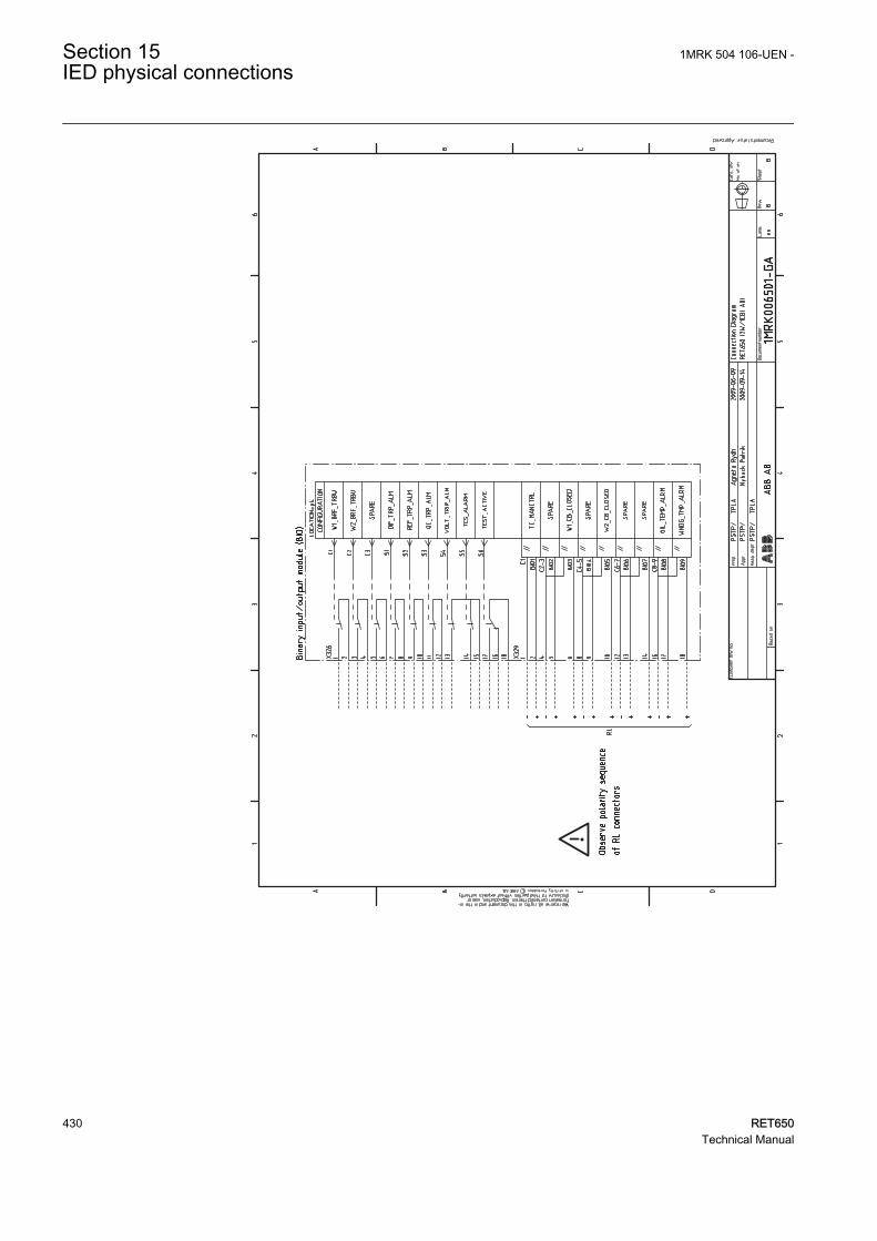
1MRK006501-GA 8 V1 EN
Section 15 1MRK 504 106-UEN -IED physical connections
430 RET650Technical Manual

Connection diagrams for RET650 A05
1MRK006501-FA 1 V1 EN
1MRK 504 106-UEN - Section 15IED physical connections
RET650 431Technical Manual

1MRK006501-FA 2 V1 EN
Section 15 1MRK 504 106-UEN -IED physical connections
432 RET650Technical Manual

1MRK006501-FA 3 V1 EN
1MRK 504 106-UEN - Section 15IED physical connections
RET650 433Technical Manual

1MRK006501-FA 4 V1 EN
Section 15 1MRK 504 106-UEN -IED physical connections
434 RET650Technical Manual

1MRK006501-FA 5 V1 EN
1MRK 504 106-UEN - Section 15IED physical connections
RET650 435Technical Manual

1MRK006501-FA 6 V1 EN
Section 15 1MRK 504 106-UEN -IED physical connections
436 RET650Technical Manual

1MRK006501-FA 7 V1 EN
1MRK 504 106-UEN - Section 15IED physical connections
RET650 437Technical Manual

1MRK006501-FA 8 V1 EN
Section 15 1MRK 504 106-UEN -IED physical connections
438 RET650Technical Manual

1MRK006501-FA 9 V1 EN
1MRK 504 106-UEN - Section 15IED physical connections
RET650 439Technical Manual

Connection diagrams for RET650 A07
1MRK006501-EA 1 V1 EN
Section 15 1MRK 504 106-UEN -IED physical connections
440 RET650Technical Manual

1MRK006501-EA 2 V1 EN
1MRK 504 106-UEN - Section 15IED physical connections
RET650 441Technical Manual

1MRK006501-EA 3 V1 EN
Section 15 1MRK 504 106-UEN -IED physical connections
442 RET650Technical Manual

1MRK006501-EA 4 V1 EN
1MRK 504 106-UEN - Section 15IED physical connections
RET650 443Technical Manual

1MRK006501-EA 5 V1 EN
Section 15 1MRK 504 106-UEN -IED physical connections
444 RET650Technical Manual

1MRK006501-EA 6 V1 EN
1MRK 504 106-UEN - Section 15IED physical connections
RET650 445Technical Manual

1MRK006501-EA 7 V1 EN
Section 15 1MRK 504 106-UEN -IED physical connections
446 RET650Technical Manual

1MRK006501-EA 8 V1 EN
1MRK 504 106-UEN - Section 15IED physical connections
RET650 447Technical Manual

448

Section 16 Technical data
16.1 Dimensions
Table 396: Dimensions of the IED
Description Type ValueWidth half 19" 220 mm
Height half 19" 265.9 mm (6U)
Depth half 19" 249.5 mm
Weight half 19" box <10 kg (6U)
half 19" LHMI 1.3 kg (6U)
16.2 Power supply
Table 397: Power supply
Description Type 1 Type 2Uauxnominal 100, 110, 120, 220, 240 V AC,
50 and 60 Hz48, 60, 110, 125 V DC
110, 125, 220, 250 V DC
Uauxvariation 85...110% of Un (85...264 V AC) 80...120% of Un (38.4...150 VDC)
80...120% of Un (88...300 V DC)
Maximum load of auxiliaryvoltage supply
35 W
Ripple in the DC auxiliary voltage Max 15% of the DC value (at frequency of 100 Hz)
Maximum interruption time in theauxiliary DC voltage withoutresetting the IED
50 ms at Uaux
1MRK 504 106-UEN - Section 16Technical data
RET650 449Technical Manual

16.3 Energizing inputs
Table 398: Energizing inputs
Description ValueRated frequency 50/60 Hz
Operating range Rated frequency ± 5 Hz
Current inputs Rated current, In 0.1/0.5 A1) 1/5 A2)
Thermal withstand capability:
• Continuously 4 A 20 A
• For 1 s 100 A 500 A
• For 10 s 25 A 100 A
Dynamic current withstand:
• Half-wave value 250 A 1250 A
Input impedance <100 mΩ <10 mΩ
Voltage inputs Rated voltage 100 V/ 110 V/ 115 V/ 120 V (Parametrization)
Voltage withstand:
• Continuous 2 x Un (240 V)
• For 10 s 3 x Un (360 V)
Burden at rated voltage <0.05 VA
1) Residual current2) Phase currents or residual current
16.4 Binary inputs
Table 399: Binary inputs
Description ValueOperating range Maximum input voltage 300 V DC
Rated voltage 24...250 V DC
Current drain 1.6...1.8 mA
Power consumption/input <0.3 W
Threshold voltage 15...221 V DC (parametrizable in the range in stepsof 1% of the rated voltage)
Section 16 1MRK 504 106-UEN -Technical data
450 RET650Technical Manual

16.5 Signal outputs
Table 400: Signal output and IRF output
Description ValueRated voltage 250 V AC/DC
Continuous contact carry 5 A
Make and carry for 3.0 s 10 A
Make and carry 0.5 s 30 A
Breaking capacity when the control-circuit timeconstant L/R<40 ms, at U< 48/110/220 V DC
≤0.5 A/≤0.1 A/≤0.04 A
Minimum contact load 100 mA at 24 V AC/DC
16.6 Power outputs
Table 401: Power output relays, with or without TCS function
Description ValueRated voltage 250 V AC/DC
Continuous contact carry 8 A
Make and carry for 3.0 s 15 A
Make and carry for 0.5 s 30 A
Breaking capacity when the control-circuit timeconstant L/R<40 ms, at U< 48/110/220 V DC
≤1 A/≤0.3 A/≤0.1 A
Minimum contact load 100 mA at 24 V AC/DC
Table 402: Power output relays with TCS function
Description ValueControl voltage range 20...250 V DC
Current drain through the supervision circuit ~1.0 mA
Minimum voltage over the TCS contact 20 V DC
16.7 Data communication interfaces
Table 403: Ethernet interfaces
Ethernet interface Protocol Cable Data transfer rateLAN/HMI port (X0)1) - CAT 6 S/FTP or better 100 MBits/s
LAN1 (X1) TCP/IP protocol Fibre-optic cable withLC connector
100 MBits/s
1) Only available for the external HMI option.
1MRK 504 106-UEN - Section 16Technical data
RET650 451Technical Manual

Table 404: Fibre-optic communication link
Wave length Fibre type Connector Permitted pathattenuation1)
Distance
1300 nm MM 62.5/125μm glass fibrecore
LC <8 dB 2 km
1) Maximum allowed attenuation caused by connectors and cable together
Table 405: X4/IRIG-B interface
Type Protocol CableScrew terminal, pinrow header
IRIG-B Shielded twisted pair cableRecommended: CAT 5, Belden RS-485 (9841-9844) or Alpha Wire (Alpha 6222-6230)
Table 406: Serial rear interface
Type Counter connectorSerial port (X9) Optical serial port, snap-in (not in use)
16.8 Enclosure class
Table 407: Degree of protection of flush-mounted IED
Description ValueFront side IP 40
Rear side, connection terminals IP 20
Table 408: Degree of protection of the LHMI
Description ValueFront and side IP 42
16.9 Environmental conditions and tests
Table 409: Environmental conditions
Description ValueOperating temperature range -25...+55ºC (continuous)
Short-time service temperature range -40...+85ºC (<16h)Note: Degradation in MTBF and HMIperformance outside the temperature range of-25...+55ºC
Relative humidity <93%, non-condensing
Table continues on next page
Section 16 1MRK 504 106-UEN -Technical data
452 RET650Technical Manual

Description ValueAtmospheric pressure 86...106 kPa
Altitude up to 2000 m
Transport and storage temperature range -40...+85ºC
Table 410: Environmental tests
Description Type test value ReferenceDry heat test (humidity <50%) • 96 h at +55ºC
• 16 h at +85ºCIEC 60068-2-2
Cold test • 96 h at -25ºC• 16 h at -40ºC
IEC 60068-2-1
Damp heat test, cyclic • 6 cycles at +25…55°C,humidity 93…95%
IEC 60068-2-30
Storage test • 96 h at -40ºC• 96 h at +85ºC
IEC 60068-2-48
1MRK 504 106-UEN - Section 16Technical data
RET650 453Technical Manual

454

Section 17 IED and functionality tests
17.1 Electromagnetic compatibility tests
Table 411: Electromagnetic compatibility tests
Description Type test value Reference100 kHz and 1 MHz burstdisturbance test
IEC 61000-4-18IEC 60255-22-1, level 3
• Common mode 2.5 kV
• Differential mode 1.0 kV
Electrostatic discharge test IEC 61000-4-2IEC 60255-22-2, level 4
• Contact discharge 8 kV
• Air discharge 15 kV
Radio frequency interferencetests
• Conducted, commonmode OK
10 V (emf), f=150 kHz...80 MHz IEC 61000-4-6IEC 60255-22-6, level 3
• Radiated, amplitude-modulated
20 V/m (rms), f=80...1000 MHzand f=1.4...2.7 GHz
IEC 61000-4-3IEC 60255-22-3
Fast transient disturbance tests IEC 61000-4-4IEC 60255-22-4, class A
• Communication ports 2 kV
• Other ports 4 kV
Surge immunity test IEC 61000-4-5IEC 60255-22-5, level 4/3
• Binary inputs 2 kV line-to-earth, 1kV line-to-line
• Communication 1 kV line-to-earth
• Other ports 4 kV line-to-earth, 2 kV line-to-line
Power frequency (50 Hz)magnetic field
IEC 61000-4-8, level 5
• 3 s 1000 A/m
• Continuous 100 A/m
Table continues on next page
1MRK 504 106-UEN - Section 17IED and functionality tests
RET650 455Technical Manual

Description Type test value ReferencePower frequency immunity test
• Common mode
• Differential mode
300 V rms 150 V rms
IEC 60255-22-7, class AIEC 61000-4-16
Voltage dips and shortinterruptions
Dips:40%/200 ms70%/500 msInterruptions:0-50 ms: No restart0...∞ s : Correct behaviour atpower down
IEC 60255-11IEC 61000-4-11
Electromagnetic emission tests EN 55011, class AIEC 60255-25
• Conducted, RF-emission(mains terminal) OK
0.15...0.50 MHz < 79 dB(µV) quasi peak< 66 dB(µV) average
0.5...30 MHz < 73 dB(µV) quasi peak< 60 dB(µV) average
• Radiated RF -emission
0...230 MHz < 40 dB(µV/m) quasi peak,measured at 10 m distance
230...1000 MHz < 47 dB(µV/m) quasi peak,measured at 10 m distance
17.2 Insulation tests
Table 412: Insulation tests
Description Type test value ReferenceDielectric tests: IEC 60255-5
• Test voltage 2 kV, 50 Hz, 1 min1 kV, 50 Hz, 1min,communication
Impulse voltage test: IEC 60255-5
• Test voltage 5 kV, unipolar impulses,waveform 1.2/50 μs, sourceenergy 0.5 J1 kV, unipolar impulses,waveform 1.2/50 μs, sourceenergy 0.5 J, communication
Insulation resistancemeasurements
IEC 60255-5
• Isolation resistance >100 MΏ, 500 V DC
Protective bonding resistance IEC 60255-27
• Resistance <0.1 Ώ (60 s)
Section 17 1MRK 504 106-UEN -IED and functionality tests
456 RET650Technical Manual

17.3 Mechanical tests
Table 413: Mechanical tests
Description Reference RequirementVibration response tests(sinusoidal)
IEC 60255-21-1 Class 2
Vibration endurance test IEC60255-21-1 Class 1
Shock response test IEC 60255-21-2 Class 1
Shock withstand test IEC 60255-21-2 Class 1
Bump test IEC 60255-21-2 Class 1
Seismic test IEC 60255-21-3 Class 2
17.4 Product safety
Table 414: Product safety
Description ReferenceLV directive 2006/95/EC
Standard EN 60255-27 (2005)
17.5 EMC compliance
Table 415: EMC compliance
Description ReferenceEMC directive 2004/108/EC
Standard EN 50263 (2000)EN 60255-26 (2007)
1MRK 504 106-UEN - Section 17IED and functionality tests
RET650 457Technical Manual

458

Section 18 Time inverse characteristics
18.1 Application
In order to assure time selectivity between different overcurrent protections indifferent points in the network different time delays for the different relays arenormally used. The simplest way to do this is to use definite time delay. In moresophisticated applications current dependent time characteristics are used. Bothalternatives are shown in a simple application with three overcurrent protectionsconnected in series.
xx05000129.vsd
I> I> I>
IEC05000129 V1 EN
Figure 165: Three overcurrent protections connected in series
en05000130.vsd
Time
Fault pointposition
Stage 1
Stage 2
Stage 3
Stage 1
Stage 2
Stage 1
IEC05000130 V1 EN
Figure 166: Definite time overcurrent characteristics
1MRK 504 106-UEN - Section 18Time inverse characteristics
RET650 459Technical Manual

en05000131.vsd
Time
Fault pointposition
IEC05000131 V1 EN
Figure 167: Inverse time overcurrent characteristics with inst. function
The inverse time characteristic makes it possible to minimize the fault clearancetime and still assure the selectivity between protections.
To assure selectivity between protections there must be a time margin between theoperation time of the protections. This required time margin is dependent offollowing factors, in a simple case with two protections in series:
• Difference between pick-up time of the protections to be co-ordinated• Opening time of the breaker closest to the studied fault• Reset time of the protection• Margin dependent of the time-delay inaccuracy of the protections
Assume we have the following network case.
Section 18 1MRK 504 106-UEN -Time inverse characteristics
460 RET650Technical Manual

en05000132.vsd
I> I>
A1 B1 Feeder
Time axis
t=0 t=t1 t=t2 t=t3
IEC05000132 V1 EN
Figure 168: Selectivity steps for a fault on feeder B1
where:
t=0 is The fault occurs
t=t1 is Protection B1 trips
t=t2 is Breaker at B1 opens
t=t3 is Protection A1 resets
In the case protection B1 shall operate without any intentional delay(instantaneous). When the fault occurs the protections start to detect the faultcurrent. After the time t1 the protection B1 send a trip signal to the circuit breaker.The protection A1 starts its delay timer at the same time, with some deviation intime due to differences between the two protections. There is a possibility that A1will start before the trip is sent to the B1 circuit breaker.
At the time t2 the circuit breaker B1 has opened its primary contacts and thus thefault current is interrupted. The breaker time (t2 - t1) can differ between differentfaults. The maximum opening time can be given from manuals and test protocols.Still at t2 the timer of protection A1 is active.
At time t3 the protection A1 is reset, i.e. the timer is stopped.
In most applications it is required that the delay times shall reset as fast as possiblewhen the current fed to the protection drops below the set current level, the resettime shall be minimized. In some applications it is however beneficial to havesome type of delayed reset time of the overcurrent function. This can be the case inthe following applications:
1MRK 504 106-UEN - Section 18Time inverse characteristics
RET650 461Technical Manual

• If there is a risk of intermittent faults. If the current relay, close to the faults,starts and resets there is a risk of unselective trip from other protections in thesystem.
• Delayed resetting could give accelerated fault clearance in case of automaticreclosing to a permanent fault.
• Overcurrent protection functions are sometimes used as release criterion forother protection functions. It can often be valuable to have a reset delay toassure the release function.
18.2 Operation principle
18.2.1 Mode of operationThe function can operate in a definite time-lag mode or in a current dependentinverse time mode. For the inverse time characteristic both ANSI and IEC basedstandard curves are available.
If current in any phase exceeds the set start current value , a timer, according to theselected operating mode, is started. The component always uses the maximum ofthe three phase current values as the current level used in timing calculations.
In case of definite time-lag mode the timer will run constantly until the time isreached or until the current drops below the reset value (start value minus thehysteresis) and the reset time has elapsed.
The general expression for inverse time curves is according to equation 76.
[ ] = + ×
->
æ öç ÷ç ÷ç ÷æ ö
ç ÷ç ÷è øè ø
p
At s B k
iC
inEQUATION1189 V1 EN (Equation 76)
where:
p, A, B, C are constants defined for each curve type,
in> is the set start current for step n,
k is set time multiplier for step n and
i is the measured current.
For inverse time characteristics a time will be initiated when the current reaches theset start level. From the general expression of the characteristic the following canbe seen:
Section 18 1MRK 504 106-UEN -Time inverse characteristics
462 RET650Technical Manual

( )- × × - = ×>
æ öæ öç ÷ç ÷
è øè ø
p
op
it B k C A k
inEQUATION1190 V1 EN (Equation 77)
where:
top is the operating time of the protection
The time elapsed to the moment of trip is reached when the integral fulfilsaccording to equation 78, in addition to the constant time delay:
0
- × ³ ×>
æ öæ öç ÷ç ÷è øè ø
òpt i
C dt A kin
EQUATION1191 V1 EN (Equation 78)
For the numerical protection the sum below must fulfil the equation for trip.
1
( )
=
D × - ³ ×>
æ öæ öç ÷ç ÷è øè ø
åpn
j
i jt C A k
inEQUATION1192 V1 EN (Equation 79)
where:
j = 1 is the first protection execution cycle when a fault has beendetected, i.e. when
1i
in>
>EQUATION1193 V1 EN
Dt is the time interval between two consecutive executions of theprotection algorithm,
n is the number of the execution of the algorithm when the triptime equation is fulfilled, i.e. when a trip is given and
i (j) is the fault current at time j
For inverse time operation, the inverse time characteristic is selectable. Both theIEC and ANSI/IEEE standardized inverse time characteristics are supported.
For the IEC curves there is also a setting of the minimum time-lag of operation, seefigure 169.
1MRK 504 106-UEN - Section 18Time inverse characteristics
RET650 463Technical Manual

en05000133.vsd
tnMin
Current
Operatetime
IEC05000133 V1 EN
Figure 169: Minimum time-lag operation for the IEC curves
In order to fully comply with IEC curves definition setting parameter tMin shall beset to the value which is equal to the operating time of the selected IEC inversetime curve for measured current of twenty times the set current pickup value. Notethat the operating time value is dependent on the selected setting value for timemultiplier k.
In addition to the ANSI and IEC standardized characteristics, there are also twoadditional inverse curves available; the RI curve and the RD curve.
The RI inverse time curve emulates the characteristic of the electromechanicalASEA relay RI. The curve is described by equation 81:
[ ]0.339 0.235
=>
- ×
æ öç ÷ç ÷ç ÷è ø
kt s
ini
EQUATION1194 V1 EN (Equation 81)
where:
in> is the set start current for step n
k is set time multiplier for step n
i is the measured current
Section 18 1MRK 504 106-UEN -Time inverse characteristics
464 RET650Technical Manual

The RD inverse curve gives a logarithmic delay, as used in the Combiflexprotection RXIDG. The curve enables a high degree of selectivity required forsensitive residual earth fault current protection, with ability to detect high resistiveearth faults. The curve is described by equation 82:
[ ] 5.8 1.35 ln= - ×× >
æ öç ÷è ø
it s
k inEQUATION1195 V1 EN (Equation 82)
where:
in> is the set start current for step n,
k is set time multiplier for step n and
i is the measured current
The timer will be reset directly when the current drops below the set start currentlevel minus the hysteresis.
18.3 Inverse time characteristics
Table 416: ANSI Inverse time characteristics
Function Range or value AccuracyOperating characteristic:
( )1= + ×
-
æ öç ÷ç ÷è ø
P
At B k
I
EQUATION1249-SMALL V1 EN (Equation 83)
I = Imeasured/Iset
k = 0.05-999 in steps of 0.01unless otherwise stated
-
ANSI Extremely Inverse A=28.2, B=0.1217, P=2.0 ANSI/IEEE C37.112,class 5 + 40 ms
ANSI Very inverse A=19.61, B=0.491, P=2.0
ANSI Normal Inverse A=0.0086, B=0.0185,P=0.02, tr=0.46
ANSI Moderately Inverse A=0.0515, B=0.1140, P=0.02
ANSI Long Time Extremely Inverse A=64.07, B=0.250, P=2.0
ANSI Long Time Very Inverse A=28.55, B=0.712, P=2.0
ANSI Long Time Inverse k=(0.01-1.20) in steps of 0.01A=0.086, B=0.185, P=0.02
1MRK 504 106-UEN - Section 18Time inverse characteristics
RET650 465Technical Manual

Table 417: IEC Inverse time characteristics
Function Range or value AccuracyOperating characteristic:
( )1= ×
-
æ öç ÷ç ÷è ø
P
At k
I
EQUATION1251-SMALL V1 EN (Equation 84)
I = Imeasured/Iset
k = (0.05-1.10) in steps of0.01
-
IEC Normal Inverse A=0.14, P=0.02 IEC 60255-3, class 5 +40 ms
IEC Very inverse A=13.5, P=1.0
IEC Inverse A=0.14, P=0.02
IEC Extremely inverse A=80.0, P=2.0
IEC Short time inverse A=0.05, P=0.04
IEC Long time inverse A=120, P=1.0
Table 418: RI and RD type inverse time characteristics
Function Range or value AccuracyRI type inverse characteristic
1
0.2360.339
= ×
-
t k
IEQUATION1137-SMALL V1 EN (Equation 85)
I = Imeasured/Iset
k=(0.05-999) in steps of 0.01 IEC 60255-3, class 5 +40 ms
RD type logarithmic inverse characteristic
5.8 1.35= - ×æ öç ÷è ø
tI
Ink
EQUATION1138-SMALL V1 EN (Equation 86)
I = Imeasured/Iset
k=(0.05-1.10) in steps of 0.01 IEC 60255-3, class 5 +40 ms
Section 18 1MRK 504 106-UEN -Time inverse characteristics
466 RET650Technical Manual

Table 419: Inverse time characteristics for Two step undervoltage protection UV2PTUV
Function Range or value AccuracyType A curve:
=< -
<
æ öç ÷è ø
kt
U U
U
EQUATION1431-SMALL V1 EN (Equation 87)
U< = UsetU = UVmeasured
k = (0.05-1.10) insteps of 0.01
Class 5 +40 ms
Type B curve:
2.0
4800.055
32 0.5
×= +
< -× -
<
æ öç ÷è ø
kt
U U
U
EQUATION1432-SMALL V1 EN (Equation 88)
U< = UsetU = Umeasured
k = (0.05-1.10) insteps of 0.01
Table 420: Inverse time characteristics for Two step overvoltage protection OV2PTOV
Function Range or value AccuracyType A curve:
=- >
>
æ öç ÷è ø
tk
U U
U
EQUATION1436-SMALL V1 EN (Equation 89)
U> = UsetU = Umeasured
k = (0.05-1.10) insteps of 0.01
Class 5 +40 ms
Type B curve:
2.0
480
32 0.5 0.035
=×
- >× - -
>
æ öç ÷è ø
tk
U U
U
EQUATION1437-SMALL V1 EN (Equation 90)
k = (0.05-1.10) insteps of 0.01
Type C curve:
3.0
480
32 0.5 0.035
=×
- >× - -
>
æ öç ÷è ø
tk
U U
U
EQUATION1438-SMALL V1 EN (Equation 91)
k = (0.05-1.10) insteps of 0.01
1MRK 504 106-UEN - Section 18Time inverse characteristics
RET650 467Technical Manual

Table 421: Inverse time characteristics for Two step residual overvoltage protection ROV2PTOV
Function Range or value AccuracyType A curve:
=- >
>
æ öç ÷è ø
tk
U U
U
EQUATION1436-SMALL V1 EN (Equation 92)
U> = UsetU = Umeasured
k = (0.05-1.10) in steps of0.01
Class 5 +40 ms
Type B curve:
2.0
480
32 0.5 0.035
=×
- >× - -
>
æ öç ÷è ø
tk
U U
U
EQUATION1437-SMALL V1 EN (Equation 93)
k = (0.05-1.10) in steps of0.01
Type C curve:
3.0
480
32 0.5 0.035
=×
- >× - -
>
æ öç ÷è ø
tk
U U
U
EQUATION1438-SMALL V1 EN (Equation 94)
k = (0.05-1.10) in steps of0.01
Section 18 1MRK 504 106-UEN -Time inverse characteristics
468 RET650Technical Manual

A070750 V2 EN
Figure 170: ANSI Extremely inverse time characteristics
1MRK 504 106-UEN - Section 18Time inverse characteristics
RET650 469Technical Manual

A070751 V2 EN
Figure 171: ANSI Very inverse time characteristics
Section 18 1MRK 504 106-UEN -Time inverse characteristics
470 RET650Technical Manual

A070752 V2 EN
Figure 172: ANSI Normal inverse time characteristics
1MRK 504 106-UEN - Section 18Time inverse characteristics
RET650 471Technical Manual

A070753 V2 EN
Figure 173: ANSI Moderately inverse time characteristics
Section 18 1MRK 504 106-UEN -Time inverse characteristics
472 RET650Technical Manual

A070817 V2 EN
Figure 174: ANSI Long time extremely inverse time characteristics
1MRK 504 106-UEN - Section 18Time inverse characteristics
RET650 473Technical Manual

A070818 V2 EN
Figure 175: ANSI Long time very inverse time characteristics
Section 18 1MRK 504 106-UEN -Time inverse characteristics
474 RET650Technical Manual

A070819 V2 EN
Figure 176: ANSI Long time inverse time characteristics
1MRK 504 106-UEN - Section 18Time inverse characteristics
RET650 475Technical Manual

A070820 V2 EN
Figure 177: IEC Normal inverse time characteristics
Section 18 1MRK 504 106-UEN -Time inverse characteristics
476 RET650Technical Manual

A070821 V2 EN
Figure 178: IEC Very inverse time characteristics
1MRK 504 106-UEN - Section 18Time inverse characteristics
RET650 477Technical Manual

A070822 V2 EN
Figure 179: IEC Inverse time characteristics
Section 18 1MRK 504 106-UEN -Time inverse characteristics
478 RET650Technical Manual

A070823 V2 EN
Figure 180: IEC Extremely inverse time characteristics
1MRK 504 106-UEN - Section 18Time inverse characteristics
RET650 479Technical Manual

A070824 V2 EN
Figure 181: IEC Short time inverse time characteristics
Section 18 1MRK 504 106-UEN -Time inverse characteristics
480 RET650Technical Manual

A070825 V2 EN
Figure 182: IEC Long time inverse time characteristics
1MRK 504 106-UEN - Section 18Time inverse characteristics
RET650 481Technical Manual

A070826 V2 EN
Figure 183: RI-type inverse time characteristics
Section 18 1MRK 504 106-UEN -Time inverse characteristics
482 RET650Technical Manual

A070827 V2 EN
Figure 184: RD-type inverse time characteristics
1MRK 504 106-UEN - Section 18Time inverse characteristics
RET650 483Technical Manual

GUID-ACF4044C-052E-4CBD-8247-C6ABE3796FA6 V1 EN
Figure 185: Inverse curve A characteristic of overvoltage protection
Section 18 1MRK 504 106-UEN -Time inverse characteristics
484 RET650Technical Manual

GUID-F5E0E1C2-48C8-4DC7-A84B-174544C09142 V1 EN
Figure 186: Inverse curve B characteristic of overvoltage protection
1MRK 504 106-UEN - Section 18Time inverse characteristics
RET650 485Technical Manual

GUID-A9898DB7-90A3-47F2-AEF9-45FF148CB679 V1 EN
Figure 187: Inverse curve C characteristic of overvoltage protection
Section 18 1MRK 504 106-UEN -Time inverse characteristics
486 RET650Technical Manual

GUID-35F40C3B-B483-40E6-9767-69C1536E3CBC V1 EN
Figure 188: Inverse curve A characteristic of undervoltage protection
1MRK 504 106-UEN - Section 18Time inverse characteristics
RET650 487Technical Manual

GUID-B55D0F5F-9265-4D9A-A7C0-E274AA3A6BB1 V1 EN
Figure 189: Inverse curve B characteristic of undervoltage protection
Section 18 1MRK 504 106-UEN -Time inverse characteristics
488 RET650Technical Manual

Section 19 Glossary
AC Alternating current
ACT Application configuration tool within PCM600
A/D converter Analog to digital converter
ADBS Amplitude dead-band supervision
ANSI American National Standards Institute
AR Autoreclosing
ASCT Auxiliary summation current transformer
ASD Adaptive signal detection
AWG American Wire Gauge standard
BR External bi-stable relay
BS British standard
CAN Controller Area Network. ISO standard (ISO 11898) forserial communication
CB Circuit breaker
CCITT Consultative Committee for International Telegraph andTelephony. A United Nations sponsored standards bodywithin the International Telecommunications Union.
CCVT Capacitive Coupled Voltage Transformer
Class C Protection Current Transformer class as per IEEE/ ANSI
CMPPS Combined mega pulses per second
CO cycle Close-open cycle
Co-directional Way of transmitting G.703 over a balanced line. Involvestwo twisted pairs making it possible to transmit informationin both directions
COMTRADE Standard format according to IEC 60255-24
Contra-directional Way of transmitting G.703 over a balanced line. Involvesfour twisted pairs of with two are used for transmitting datain both directions, and two pairs for transmitting clock signals
CPU Central processor unit
CR Carrier receive
CRC Cyclic redundancy check
CS Carrier send
1MRK 504 106-UEN - Section 19Glossary
RET650 489Technical Manual

CT Current transformer
CVT Capacitive voltage transformer
DAR Delayed auto-reclosing
DARPA Defense Advanced Research Projects Agency (The USdeveloper of the TCP/IP protocol etc.)
DBDL Dead bus dead line
DBLL Dead bus live line
DC Direct current
DFT Discrete Fourier transform
DIP-switch Small switch mounted on a printed circuit board
DLLB Dead line live bus
DNP Distributed Network Protocol as per IEEE/ANSI Std.1379-2000
DR Disturbance recorder
DRAM Dynamic random access memory
DRH Disturbance report handler
DSP Digital signal processor
DTT Direct transfer trip scheme
EHV network Extra high voltage network
EIA Electronic Industries Association
EMC Electro magnetic compatibility
EMF Electro motive force
EMI Electro magnetic interference
EnFP End fault protection
ESD Electrostatic discharge
FOX 20 Modular 20 channel telecommunication system for speech,data and protection signals
FOX 512/515 Access multiplexer
FOX 6Plus Compact, time-division multiplexer for the transmission ofup to seven duplex channels of digital data over optical fibers
G.703 Electrical and functional description for digital lines used bylocal telephone companies. Can be transported over balancedand unbalanced lines
GCM Communication interface module with carrier of GPSreceiver module
GDE Graphical display editor within PCM600
Section 19 1MRK 504 106-UEN -Glossary
490 RET650Technical Manual

GI General interrogation command
GIS Gas insulated switchgear
GOOSE Generic object oriented substation event
GPS Global positioning system
HDLC protocol High level data link control, protocol based on the HDLCstandard
HFBR connectortype
Plastic fiber connector
HMI Human machine interface
HSAR High speed auto reclosing
HV High voltage
HVDC High voltage direct current
IDBS Integrating dead band supervision
IEC International Electrical Committee
IEC 60044-6 IEC Standard, Instrument transformers – Part 6:Requirements for protective current transformers fortransient performance
IEC 61850 Substation Automation communication standard
IEEE Institute of Electrical and Electronics Engineers
IEEE 802.12 A network technology standard that provides 100 Mbits/s ontwisted-pair or optical fiber cable
IEEE P1386.1 PCI Mezzanine card (PMC) standard for local bus modules.References the CMC (IEEE P1386, also known as Commonmezzanine card) standard for the mechanics and the PCIspecifications from the PCI SIG (Special Interest Group) forthe electrical EMF Electro Motive Force.
IED Intelligent electronic device
I-GIS Intelligent gas insulated switchgear
Instance When several occurrences of the same function are availablein the IED they are referred to as instances of that function.One instance of a function is identical to another of the samekind but will have a different number in the IED userinterfaces. The word instance is sometimes defined as anitem of information that is representative of a type. In thesame way an instance of a function in the IED isrepresentative of a type of function.
IP 1. Internet protocol. The network layer for the TCP/IPprotocol suite widely used on Ethernet networks. IP is aconnectionless, best-effort packet switching protocol. It
1MRK 504 106-UEN - Section 19Glossary
RET650 491Technical Manual

provides packet routing, fragmentation and re-assemblythrough the data link layer.2. Ingression protection according to IEC standard
IP 20 Ingression protection, according to IEC standard, level 20
IP 40 Ingression protection, according to IEC standard, level 40
IP 54 Ingression protection, according to IEC standard, level 54
IRF Internal fail signal
IRIG-B: InterRange Instrumentation Group Time code format B,standard 200
ITU International Telecommunications Union
LAN Local area network
LIB 520 High voltage software module
LCD Liquid crystal display
LDD Local detection device
LED Light emitting diode
MCB Miniature circuit breaker
MCM Mezzanine carrier module
MVB Multifunction vehicle bus. Standardized serial bus originallydeveloped for use in trains.
NCC National Control Centre
OCO cycle Open-close-open cycle
OCP Overcurrent protection
OLTC On load tap changer
OV Over voltage
Overreach A term used to describe how the relay behaves during a faultcondition. For example a distance relay is over-reachingwhen the impedance presented to it is smaller than theapparent impedance to the fault applied to the balance point,i.e. the set reach. The relay “sees” the fault but perhaps itshould not have seen it.
PCI Peripheral component interconnect, a local data bus
PCM Pulse code modulation
PCM600 Protection and control IED manager
PC-MIP Mezzanine card standard
PISA Process interface for sensors & actuators
PMC PCI Mezzanine card
POTT Permissive overreach transfer trip
Section 19 1MRK 504 106-UEN -Glossary
492 RET650Technical Manual

Process bus Bus or LAN used at the process level, that is, in nearproximity to the measured and/or controlled components
PSM Power supply module
PST Parameter setting tool within PCM600
PT ratio Potential transformer or voltage transformer ratio
PUTT Permissive underreach transfer trip
RASC Synchrocheck relay, COMBIFLEX
RCA Relay characteristic angle
REVAL Evaluation software
RFPP Resistance for phase-to-phase faults
RFPE Resistance for phase-to-earth faults
RISC Reduced instruction set computer
RMS value Root mean square value
RS422 A balanced serial interface for the transmission of digitaldata in point-to-point connections
RS485 Serial link according to EIA standard RS485
RTC Real time clock
RTU Remote terminal unit
SA Substation Automation
SC Switch or push-button to close
SCS Station control system
SCT System configuration tool according to standard IEC 61850
SMA connector Subminiature version A, A threaded connector with constantimpedance.
SMT Signal matrix tool within PCM600
SMS Station monitoring system
SNTP Simple network time protocol – is used to synchronizecomputer clocks on local area networks. This reduces therequirement to have accurate hardware clocks in everyembedded system in a network. Each embedded node caninstead synchronize with a remote clock, providing therequired accuracy.
SRY Switch for CB ready condition
ST Switch or push-button to trip
Starpoint Neutral point of transformer or generator
SVC Static VAr compensation
TC Trip coil
1MRK 504 106-UEN - Section 19Glossary
RET650 493Technical Manual

TCS Trip circuit supervision
TCP Transmission control protocol. The most common transportlayer protocol used on Ethernet and the Internet.
TCP/IP Transmission control protocol over Internet Protocol. The defacto standard Ethernet protocols incorporated into 4.2BSDUnix. TCP/IP was developed by DARPA for internetworking and encompasses both network layer and transportlayer protocols. While TCP and IP specify two protocols atspecific protocol layers, TCP/IP is often used to refer to theentire US Department of Defense protocol suite based uponthese, including Telnet, FTP, UDP and RDP.
TNC connector Threaded Neill Concelman, A threaded constant impedanceversion of a BNC connector
TPZ, TPY, TPX,TPS
Current transformer class according to IEC
Underreach A term used to describe how the relay behaves during a faultcondition. For example a distance relay is under-reachingwhen the impedance presented to it is greater than theapparent impedance to the fault applied to the balance point,i.e. the set reach. The relay does not “see” the fault butperhaps it should have seen it. See also Overreach.
U/I-PISA Process interface components that deliver measured voltageand current values
UTC Coordinated universal time. A coordinated time scale,maintained by the Bureau International des Poids et Mesures(BIPM), which forms the basis of a coordinateddissemination of standard frequencies and time signals. UTCis derived from International Atomic Time (TAI) by theaddition of a whole number of "leap seconds" to synchronizeit with Universal Time 1 (UT1), thus allowing for theeccentricity of the Earth"s orbit, the rotational axis tilt (23.5degrees), but still showing the Earth"s irregular rotation, onwhich UT1 is based. The Coordinated Universal Time isexpressed using a 24-hour clock and uses the Gregoriancalendar. It is used for aeroplane and ship navigation, whereit also sometimes known by the military name, "Zulu time"."Zulu" in the phonetic alphabet stands for "Z" which standsfor longitude zero.
UV Undervoltage
WEI Weak end infeed logic
VT Voltage transformer
X.21 A digital signalling interface primarily used for telecomequipment
Section 19 1MRK 504 106-UEN -Glossary
494 RET650Technical Manual

3IO Three times zero-sequence current. Often referred to as theresidual or the earth-fault current
3UO Three times the zero sequence voltage. Often referred to asthe residual voltage or the neutral point voltage
1MRK 504 106-UEN - Section 19Glossary
RET650 495Technical Manual

496

497

Contact us
ABB ABSubstation Automation ProductsSE-721 59 Västerås, SwedenPhone +48 (0) 21 34 20 00Fax +48 (0) 21 14 69 18
www.abb.com/substationautomation
1MR
K 5
04 1
06-U
EN
-©
Cop
yrig
ht 2
009
AB
B. A
ll rig
hts
rese
rved
.


