Embed Size (px)
Citation preview
1
Adv CMPE 640
Co
also on the preceding
via storage elements.
nostable and astable cir-
ential library element
ile a monostable multi-
anced VLSI Design Sequential Logic Design
ncepts
In sequential logic, the outputs depend not only on the inputs, but input values... it has memory.
Memory can be implemented in 2 ways: Positive feedback or regeneration (static):
One or more output signals are connected back to the inputs These circuits are called multivibrator.Bistable elements such as flip-flops are most common but mo
cuits are also used. Charge storage (dynamic):
As we know, a periodic refresh is necessary here.
The bistable element can be either static or dynamic and is an esscalled a register.
An astable multivibrator acts as an oscillator (clock generator) whvibrator can be used as a pulse generator.
2
Adv CMPE 640
Sta
n 1, there are only two
a duration equal to the
e region where the gain,
in
ive
finv(Vi2)
Metastable
anced VLSI Design Sequential Logic Design
tic Sequential Circuits
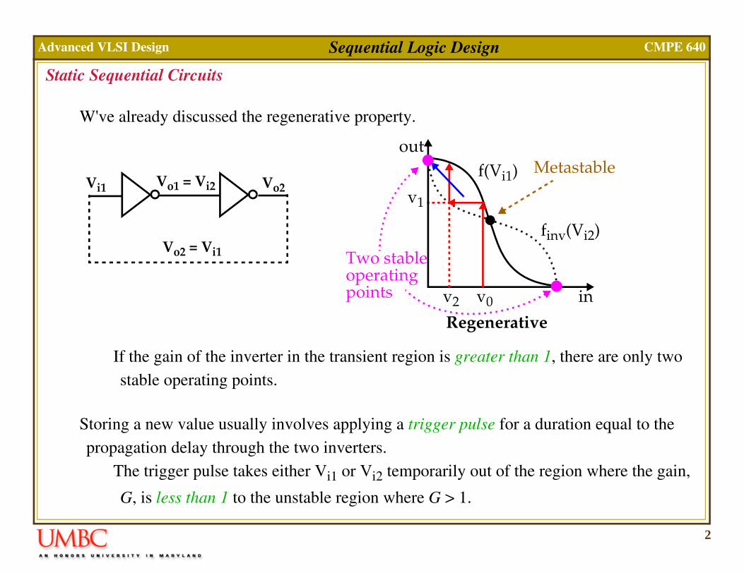
W've already discussed the regenerative property.
If the gain of the inverter in the transient region is greater tha
stable operating points.
Storing a new value usually involves applying a trigger pulse for propagation delay through the two inverters.
The trigger pulse takes either Vi1 or Vi2 temporarily out of th
G, is less than 1 to the unstable region where G > 1.
Vo1 = Vi2Vi1 Vo2
Vo2 = Vi1
out
Regenerat
v0
v1
v2
f(Vi1)
Two stable operating points
3
Adv CMPE 640
Fl
ode is forbiddenaint Q and Q
entary. Also,/11 leaves the FFable state.
SF
anced VLSI Design Sequential Logic Design
ip-flop Classification
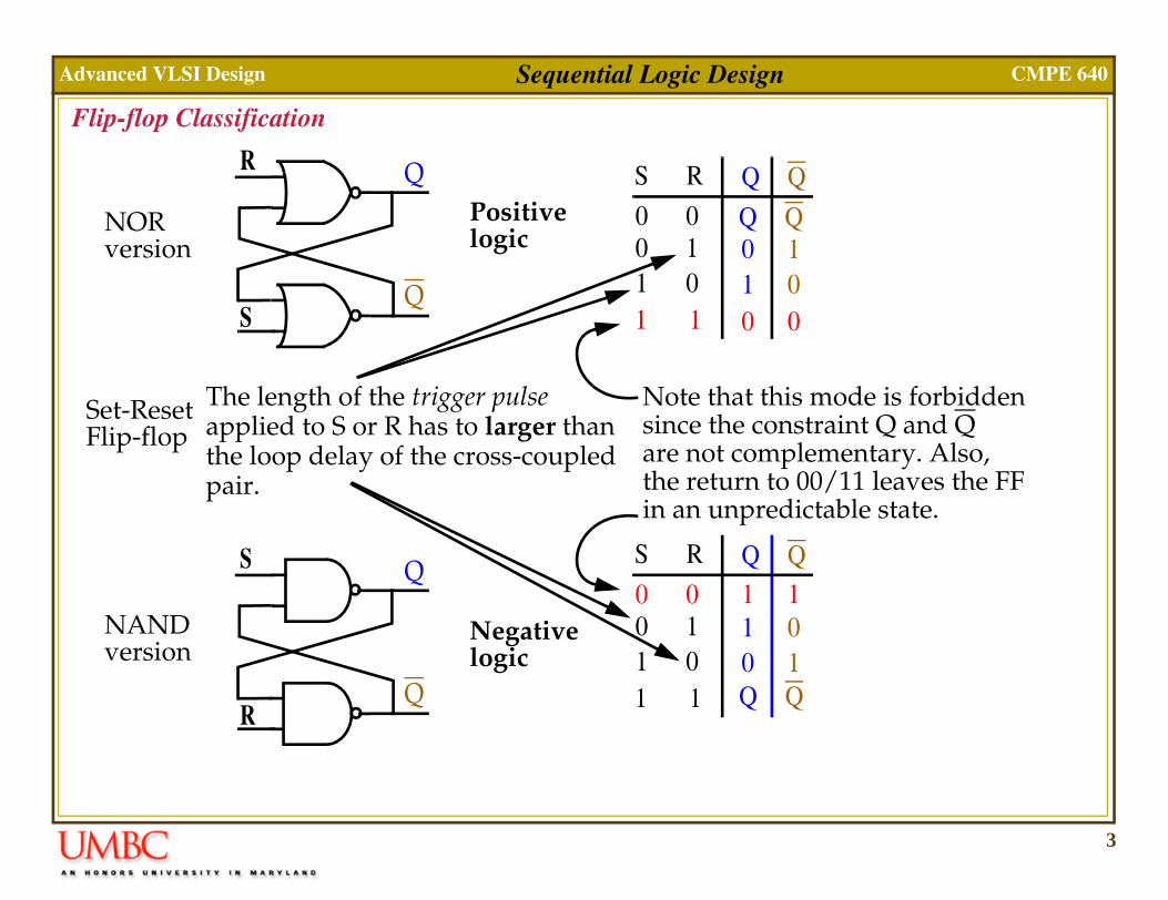
R
S
S R Q
0 0 Q0 1 01 0 11 1 0
Q
NOR
Q
Q
Q100
version
The length of the trigger pulse applied to S or R has to larger thanthe loop delay of the cross-coupledpair.
Note that this msince the constrare not complemthe return to 00in an unpredict
S
R
Q
Q
S R Q
0 0
Q
0 1 11 0 01 1
Q
Q
01
1 1
et-Resetlip-flop
NANDversion
Positivelogic
Negativelogic
4
Adv CMPE 640
Fl
lses going active simul-
lemented.
.g. < than the propaga-
n+1
n
n
stic table isxcept forde
anced VLSI Design Sequential Logic Design
ip-flop Classification
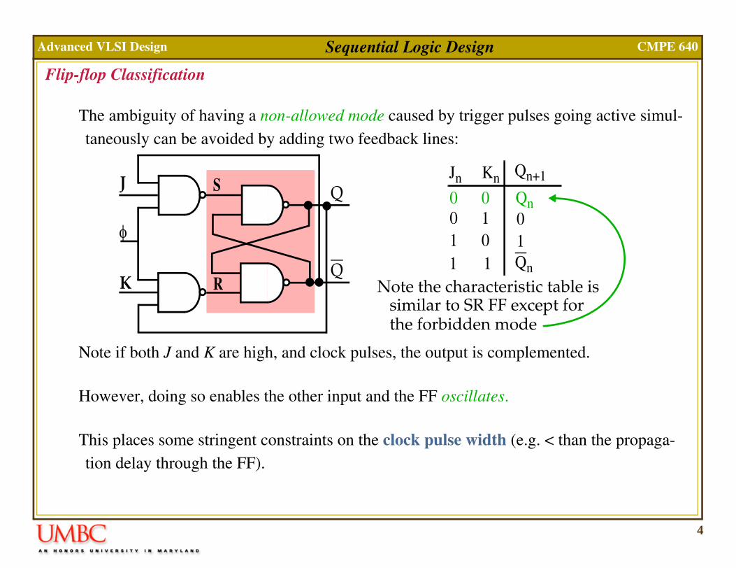
The ambiguity of having a non-allowed mode caused by trigger putaneously can be avoided by adding two feedback lines:
Note if both J and K are high, and clock pulses, the output is comp
However, doing so enables the other input and the FF oscillates.
This places some stringent constraints on the clock pulse width (etion delay through the FF).
Jn Kn Q
0 0
Q
0 1 01 0 11 1
Q
Note the characterisimilar to SR FF ethe forbidden mo
S
R
Q
QK
J
φ
5
Adv CMPE 640
Fl
with the clock signal, φ.
gether.omplementary values of
the clock.
h (low).l delay.
anced VLSI Design Sequential Logic Design
ip-flop Classification
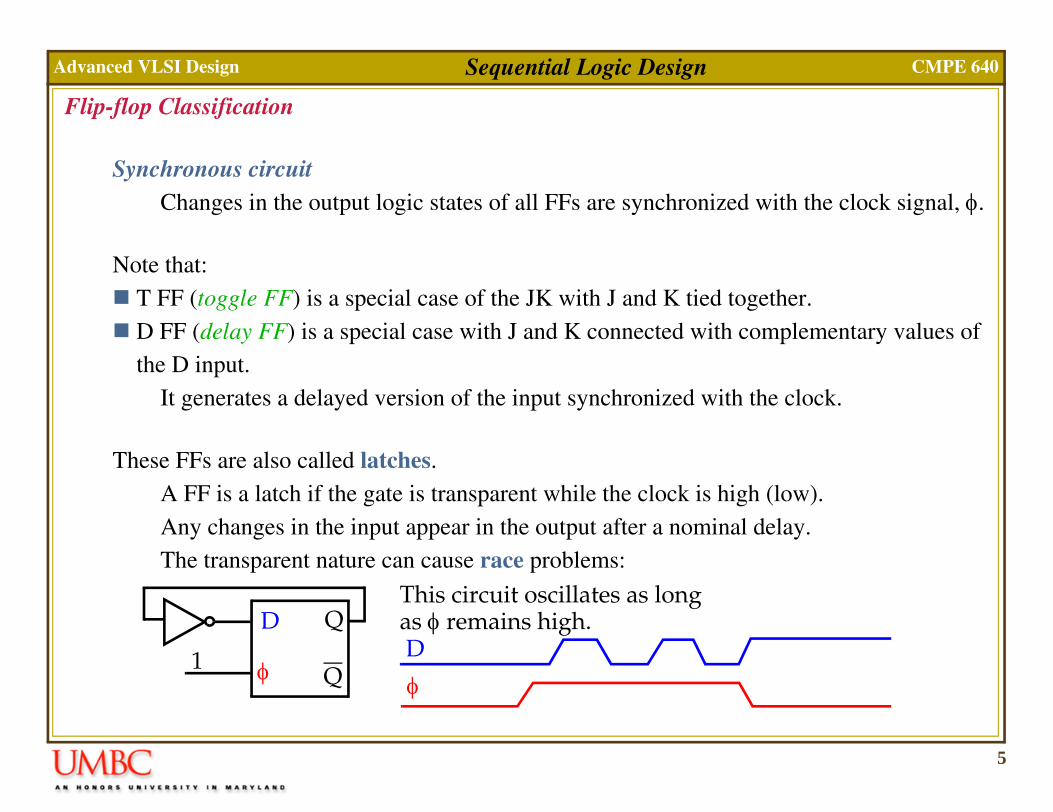
Synchronous circuitChanges in the output logic states of all FFs are synchronized
Note that: T FF (toggle FF) is a special case of the JK with J and K tied to D FF (delay FF) is a special case with J and K connected with cthe D input.
It generates a delayed version of the input synchronized with
These FFs are also called latches.A FF is a latch if the gate is transparent while the clock is higAny changes in the input appear in the output after a nominaThe transparent nature can cause race problems:
D
φ
Q
Q1
This circuit oscillates as longas φ remains high.
φ
D

6
Adv CMPE 640
Ma
gh. SI and RI from propagat-
gates in the slave are
r operation.
Q
Q
anced VLSI Design Sequential Logic Design
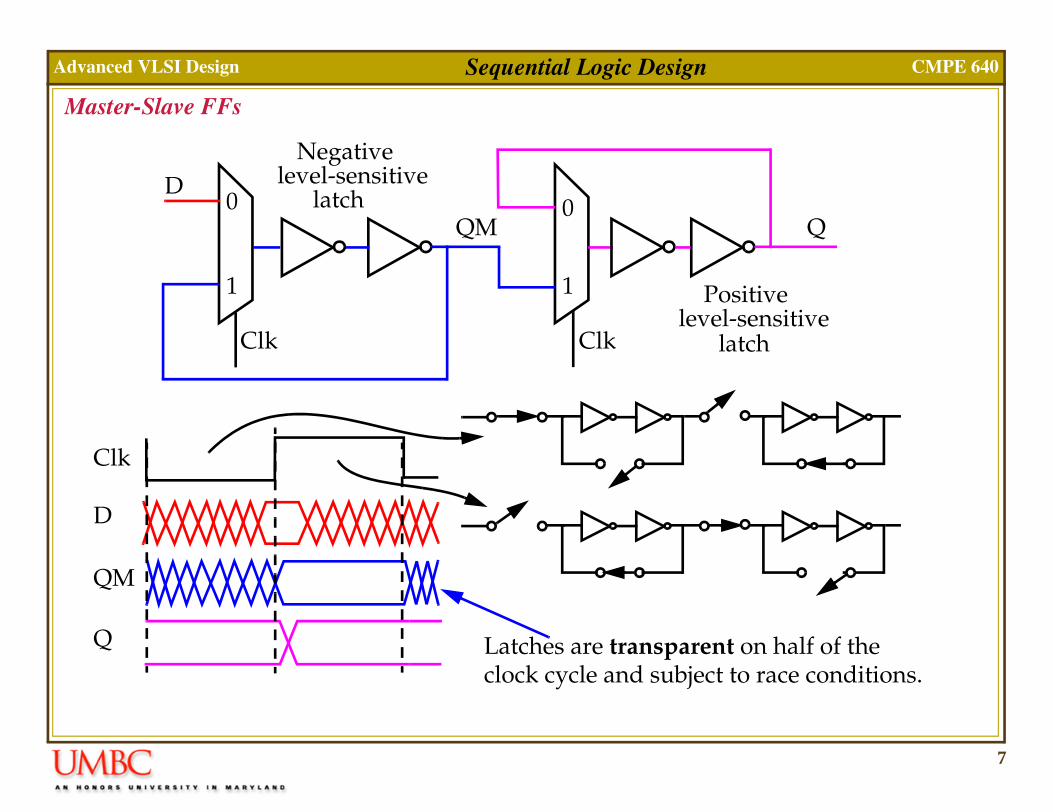
ster-Slave FFsOne way to avoid the race is to use the master-slave approach.
The master on the left is active (J and K are enabled) when φ is hiThe slave on the right is in hold mode, preventing changes oning to the output, Q.
When φ goes low, the state of the master is frozen and the NANDenabled.
There is no constraint on the maximum width of φ for prope
SI
RIK
J
φ
Master Slave
7
Adv CMPE 640
Ma
Q
on half of the
itiveensitivech
race conditions.
anced VLSI Design Sequential Logic Design
ster-Slave FFs
0
1
D0
1
QM
Clk Clk
Clk
D
QM
Q Latches are transparent
Negativelevel-sensitive
Poslevel-s
latch
lat
clock cycle and subject to
8
Adv CMPE 640
Ma
Q
Clr
Q
Q
anced VLSI Design Sequential Logic Design
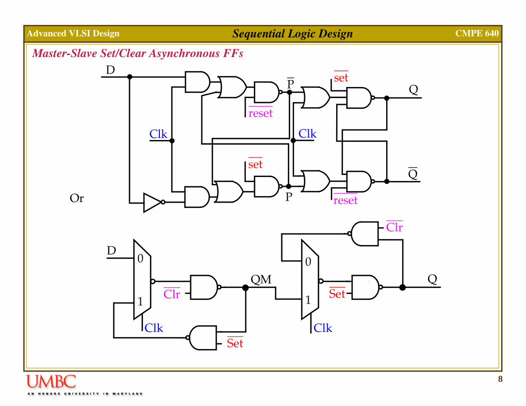
ster-Slave Set/Clear Asynchronous FFs
Or
0
1
D0
1
QM
Clk Clk
Clr
Set
Set
Clk
reset
P
P
set
reset
Clk
setD
9
Adv CMPE 640
To
anced VLSI Design Sequential Logic Design
ggle Flip-Flop with Asynchronous Clear:
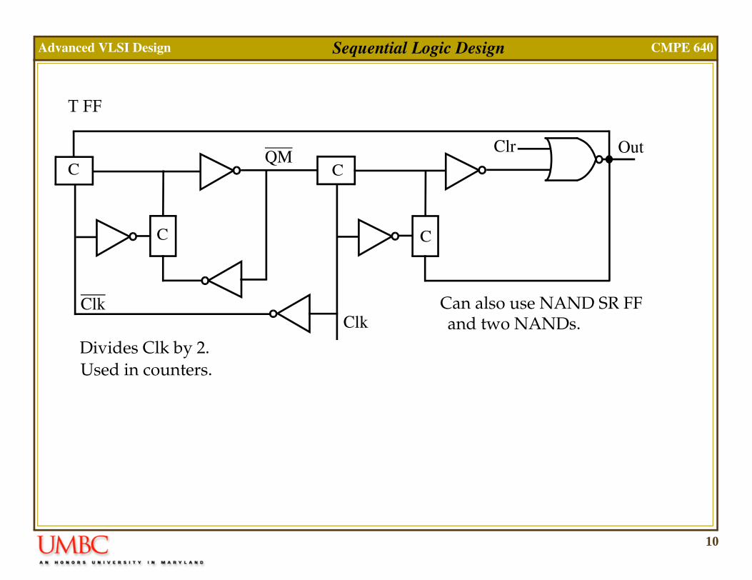
10
Adv CMPE 640
Out
ANDs. NAND SR FF
anced VLSI Design Sequential Logic Design
C
Clk
QM
C
C
C
Used in counters.
Clk
Clr
and two NCan also use
T FF
Divides Clk by 2.
11
Adv CMPE 640
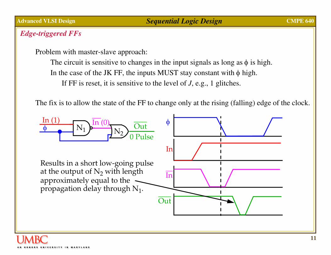
Ed
as φ is high. φ high.es.
falling) edge of the clock.
anced VLSI Design Sequential Logic Design
ge-triggered FFs
Problem with master-slave approach:The circuit is sensitive to changes in the input signals as longIn the case of the JK FF, the inputs MUST stay constant with
If FF is reset, it is sensitive to the level of J, e.g., 1 glitch
The fix is to allow the state of the FF to change only at the rising (
φIn (1) In (0) Out φ
In
In
Out
Results in a short low-going pulse at the output of N2 with length
N1 N2
approximately equal to thepropagation delay through N1.
0 Pulse
12
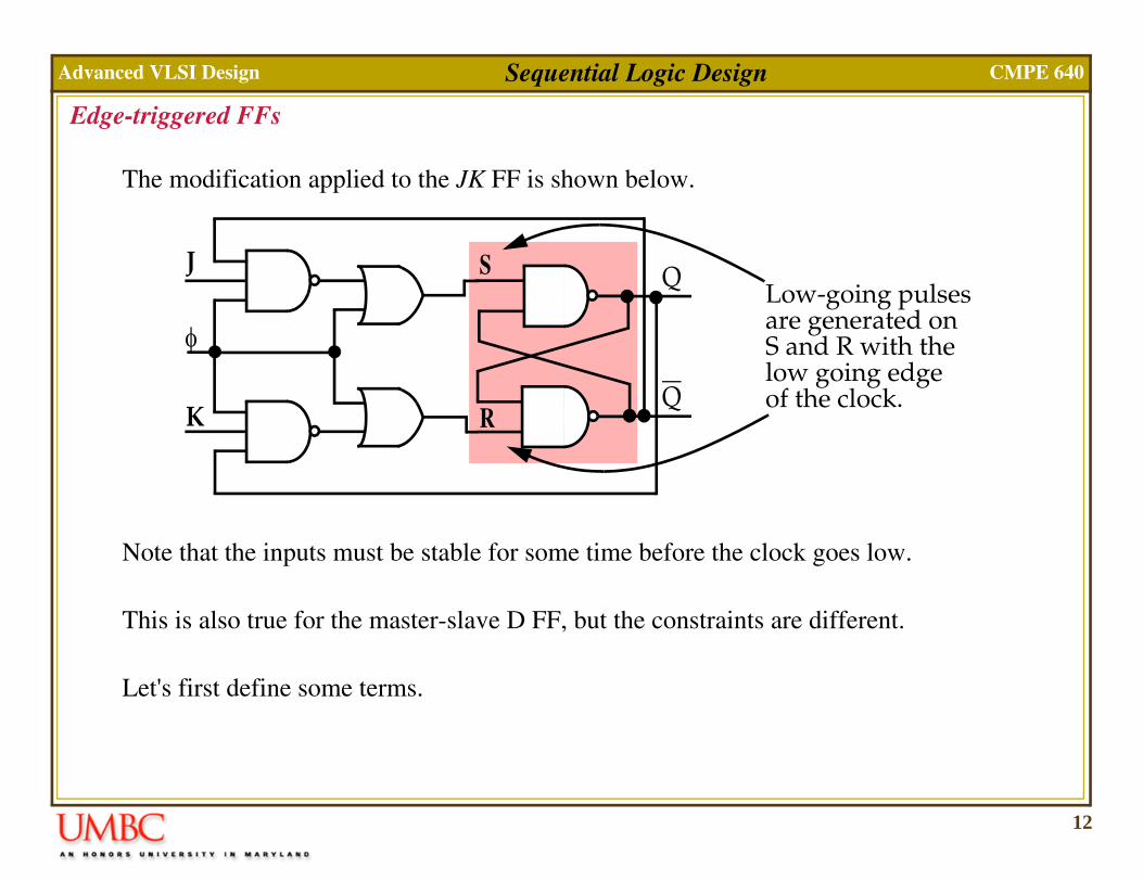
Adv CMPE 640
Ed
goes low.
different.
-going pulsesgenerated ond R with the going edgehe clock.
anced VLSI Design Sequential Logic Design
ge-triggered FFs
The modification applied to the JK FF is shown below.
Note that the inputs must be stable for some time before the clock
This is also true for the master-slave D FF, but the constraints are
Let's first define some terms.
S
R
Q
QK
J
φ
Loware S anlowof t
13
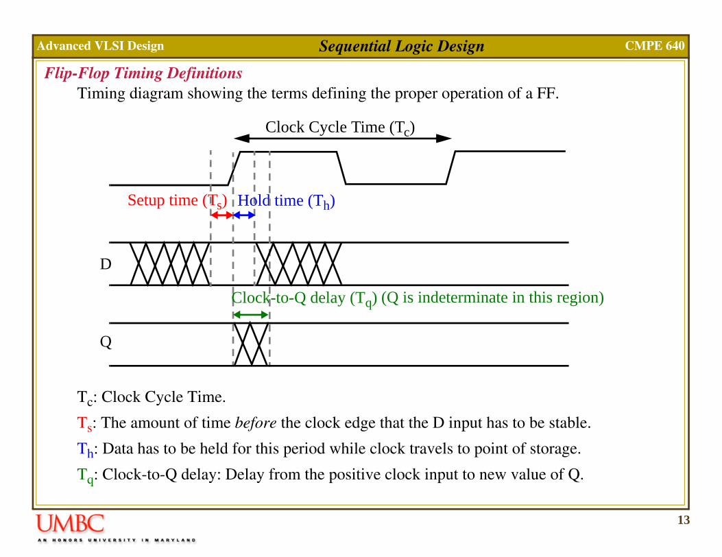
Adv CMPE 640
Flof a FF.
to be stable.
of storage.
value of Q.
in this region)
anced VLSI Design Sequential Logic Design
ip-Flop Timing DefinitionsTiming diagram showing the terms defining the proper operation
Tc: Clock Cycle Time.
Ts: The amount of time before the clock edge that the D input has
Th: Data has to be held for this period while clock travels to point
Tq: Clock-to-Q delay: Delay from the positive clock input to new
Clock Cycle Time (Tc)
Setup time (Ts) Hold time (Th)
Clock-to-Q delay (Tq)
D
(Q is indeterminate
Q
14
Adv CMPE 640
Se non-zero.
er setup time than the
ut so the FF's internal
D Q
ct" storage value. a zero will be
G1 and G2.
"t
anced VLSI Design Sequential Logic Design
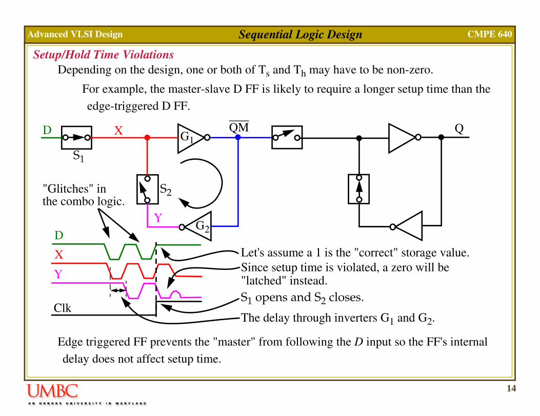
tup/Hold Time ViolationsDepending on the design, one or both of Ts and Th may have to be
For example, the master-slave D FF is likely to require a longedge-triggered D FF.
Edge triggered FF prevents the "master" from following the D inpdelay does not affect setup time.
QM
Y
X
D
X
Y
Clk
Let's assume a 1 is the "correSince setup time is violated,"latched" instead.
The delay through inverters
Glitches" inhe combo logic.
G1
G2
S1
S2
S1 opens and S2 closes.
15
Adv CMPE 640
Sy
ansparent on half of the
cycle time, Tq is the
B.
outputs
outputs
anced VLSI Design Sequential Logic Design
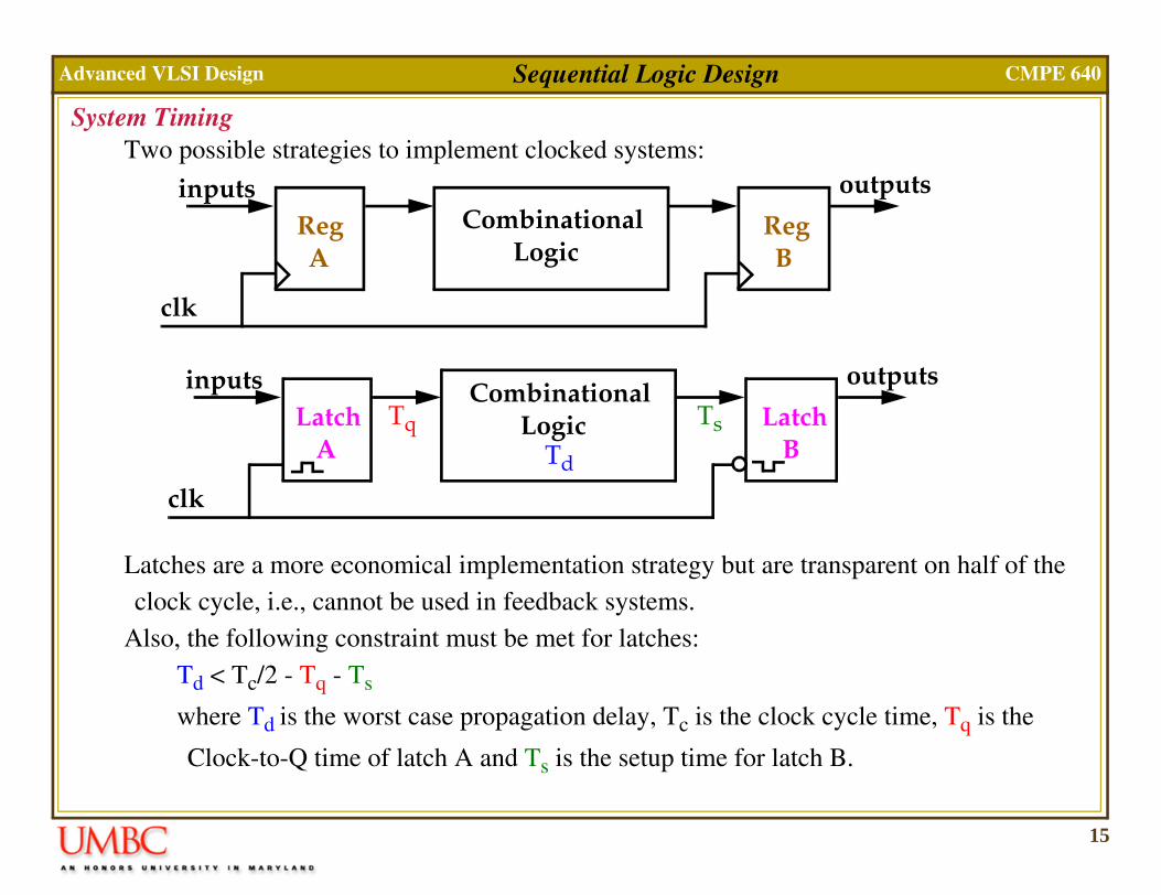
stem TimingTwo possible strategies to implement clocked systems:
Latches are a more economical implementation strategy but are trclock cycle, i.e., cannot be used in feedback systems.
Also, the following constraint must be met for latches:Td < Tc/2 - Tq - Ts
where Td is the worst case propagation delay, Tc is the clock
Clock-to-Q time of latch A and Ts is the setup time for latch
Logic
inputs
clk
CombinationalRegA
RegB
inputs
clk
CombinationalLatch
ALatch
BTq Ts
Td
Logic
16
Adv CMPE 640
Cl:
Q’
anced VLSI Design Sequential Logic Design
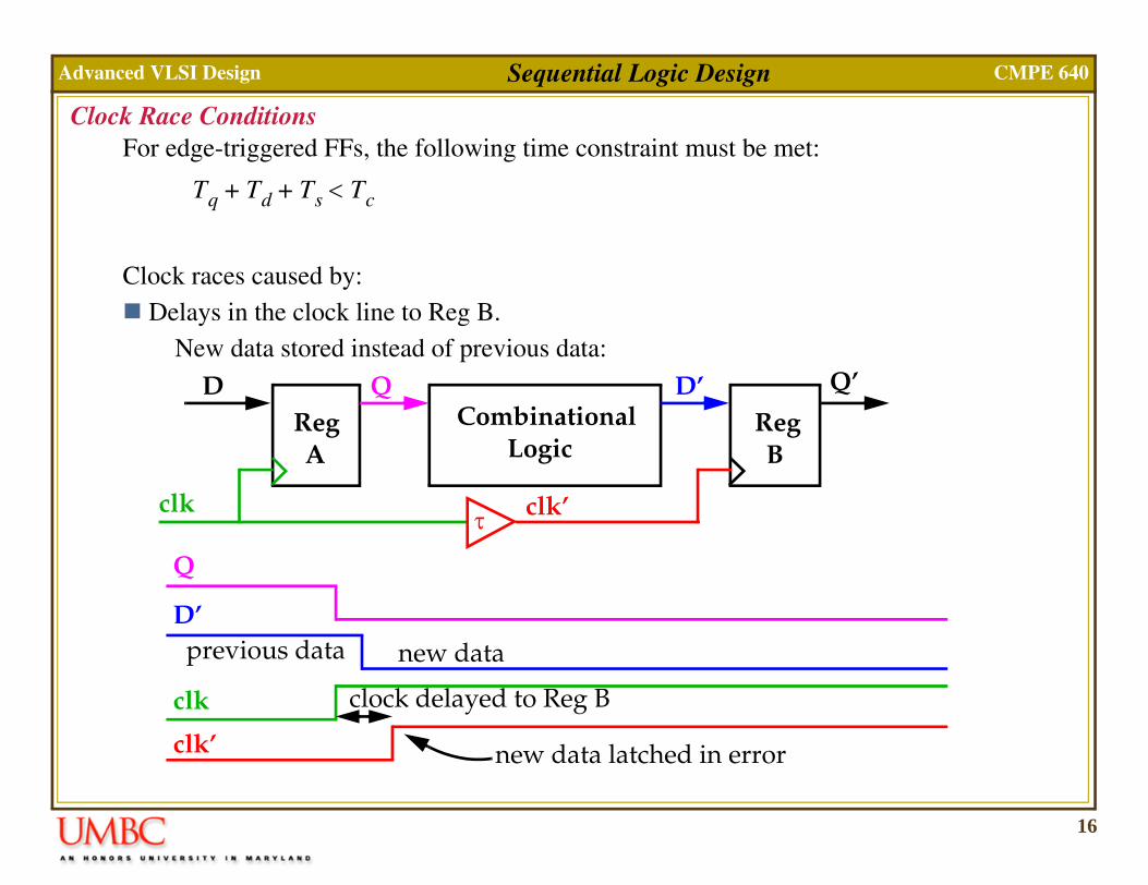
ock Race ConditionsFor edge-triggered FFs, the following time constraint must be met
Clock races caused by: Delays in the clock line to Reg B.
New data stored instead of previous data:
Tq Td Ts Tc<+ +
Logic
D
clk
CombinationalRegA
RegB
τ
Q D’
Q
D’
clk
clk’
clk’
clock delayed to Reg B
new dataprevious data
new data latched in error
17
Adv CMPE 640
Cl
cycle time.g new data.
., they have to minimize combinational logic.
Q’
ched in error.
anced VLSI Design Sequential Logic Design
ock Race Conditions
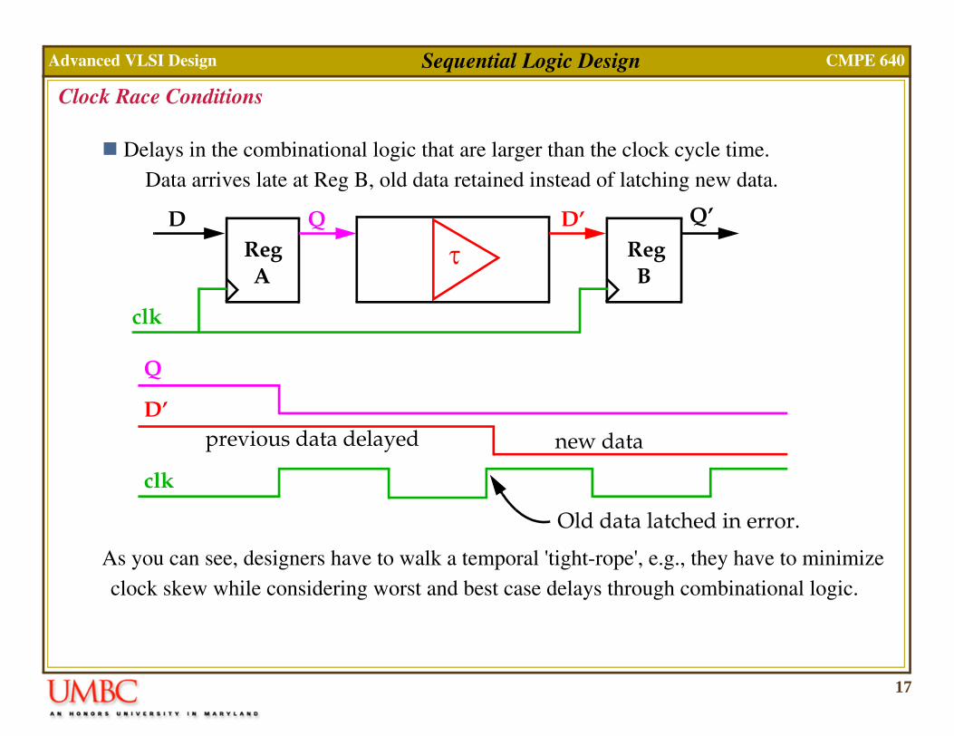
Delays in the combinational logic that are larger than the clock Data arrives late at Reg B, old data retained instead of latchin
As you can see, designers have to walk a temporal 'tight-rope', e.gclock skew while considering worst and best case delays through
D
clk
RegA
RegB
τQ D’
Q
D’
clk
new dataprevious data delayed
Old data lat
18
Adv CMPE 640
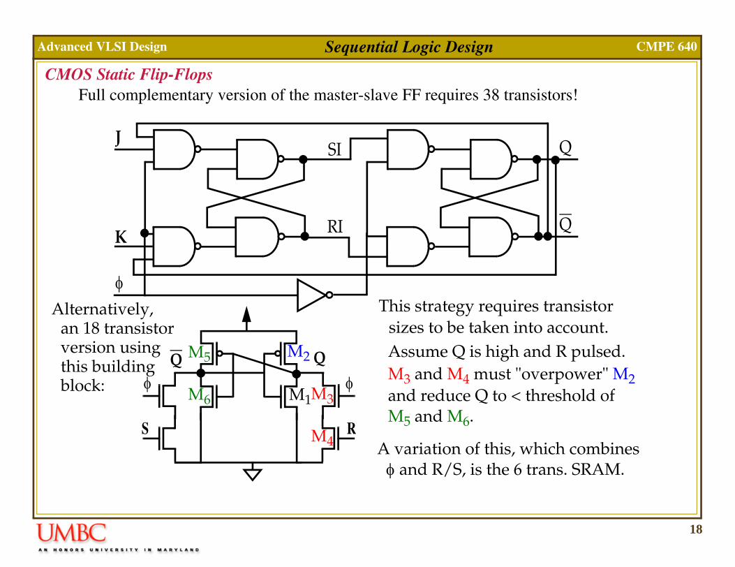
CMnsistors!
A res transistornto account. and R pulsed.overpower" M2 threshold of
which combines trans. SRAM.
Q
Q
anced VLSI Design Sequential Logic Design
OS Static Flip-FlopsFull complementary version of the master-slave FF requires 38 tra
φ
lternatively,
φQQ
RS
M1
M2
M3
M4
This strategy requisizes to be taken iAssume Q is highM3 and M4 must "and reduce Q to <
M5
M6M5 and M6.
an 18 transistorversion using
A variation of this, φ and R/S, is the 6
this buildingblock:
SI
RIK
J
φ


