Embed Size (px)
Citation preview

ELCT201: DIGITAL LOGIC DESIGN
Lecture 11
Following the slides of Dr. Ahmed H. Madian
Prof. Dr. Eng. Tallal El-Shabrawy, [email protected]
Dr. Eng. Wassim Alexan, [email protected]
هــ 1441محرم
Spring 2020
COURSE OUTLINE
1. Introduction
2. Gate-Level Minimization
3. Combinational Logic
4. Synchronous Sequential Logic
5. Registers and Counters
6. Memories and Programmable Logic
2

LECTURE OUTLINE
• Counters • Definition and Introduction
• Binary Ripple Counters
• 𝑇 FF-based
• 𝐷 FF-based
• Synchronous Counters
• Up Counters
• Down Counters
• Unused States
• Design Problems
3

COUNTERS: A DEFINITION
4
• A register that goes through a prescribed sequence of states upon the application of input pulses is called a counter
• The input pulses may be clock pulses, or they may originate from some external source and occur at a fixed interval of time or at random
• The sequence of states may follow the binary number sequence or any other sequence of states
000 → 001 → 010 → 011 → 100 → 101 → ⋯
000 → 010 → 100 → 000 → 010 → 100 → ⋯

COUNTERS: INTRODUCTION
5
• A counter that follows the binary number sequence is called a binary counter
• An 𝑛 −bit binary counter consists of 𝑛 FFs and can count from 0 through 2𝑛 − 1
• Counters are available in 2 categories:
• Ripple counters
• Synchronous counters
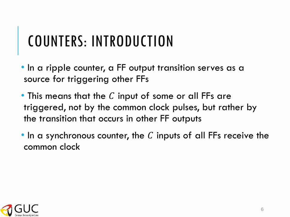
COUNTERS: INTRODUCTION
6
• In a ripple counter, a FF output transition serves as a source for triggering other FFs
• This means that the 𝐶 input of some or all FFs are triggered, not by the common clock pulses, but rather by the transition that occurs in other FF outputs
• In a synchronous counter, the 𝐶 inputs of all FFs receive the common clock

BINARY RIPPLE COUNTERS
7
• A binary ripple counter consists of a series connection of complementing FFs, with the output of each FF connected to the 𝐶 input of the next higher order FF (see next slide)
• The FF holding the least significant bit receives the incoming count pulses
• The output of the first FF is always the complement of its input
• The 𝑇 inputs of all the FFs in the first counter are permanently connected to 𝐿𝑜𝑔𝑖𝑐 1, making each FF complement if the signal in its 𝐶 input goes through a negative transition
• The negative transition occurs when the output of the previous FF to which 𝐶 is connected goes from 1 to 0

8
𝐿𝑜𝑔𝑖𝑐 1
𝑅𝑒𝑠𝑒𝑡
𝐴3
𝐴2
𝐴1
𝐴0
𝑅𝑒𝑠𝑒𝑡
𝐶𝑜𝑢𝑛𝑡
𝐴3
𝐴2
𝐴1
𝐴0
But what if we are interested
in building a counter that
counts down? How can we
modify the current logic
diagrams to achieve this new
target?
𝐶𝑜𝑢𝑛𝑡
9
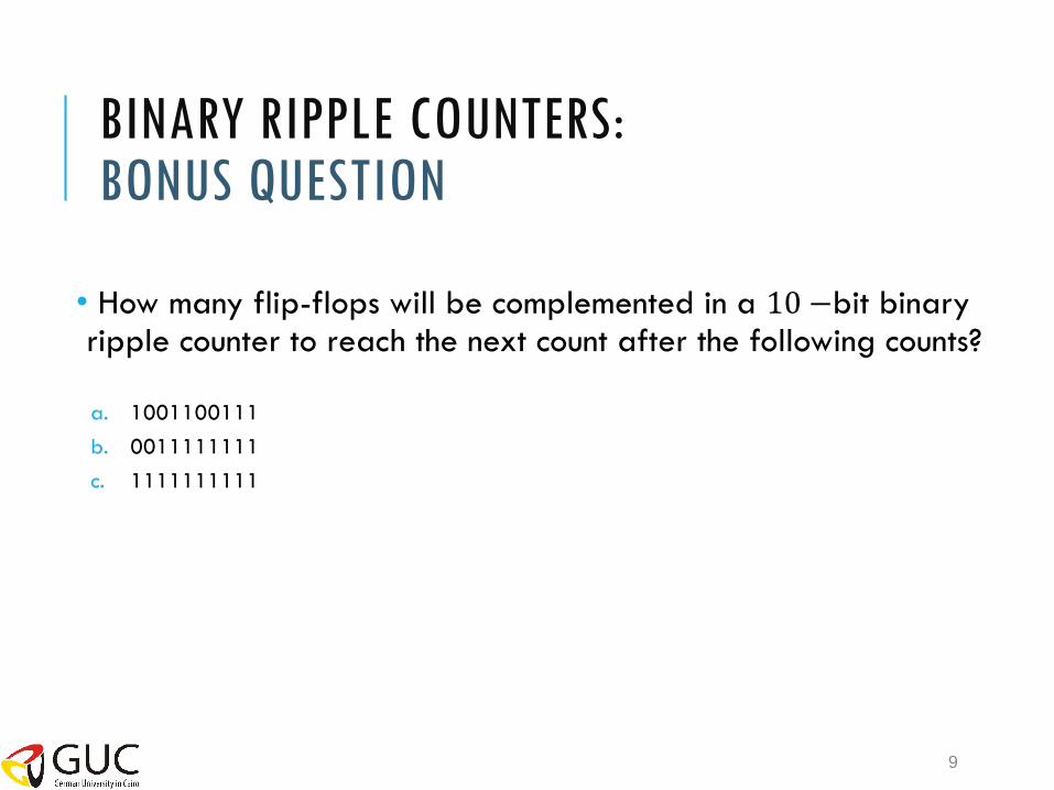
BINARY RIPPLE COUNTERS: BONUS QUESTION
• How many flip-flops will be complemented in a 10 −bit binary ripple counter to reach the next count after the following counts?
a. 1001100111
b. 0011111111
c. 1111111111

SYNCHRONOUS COUNTERS
10
• In a synchronous binary counter, the FF controlling the least significant bit is complemented with every clock cycle
• Any other FF will only complement its stored bit when all the bits in the lower significant positions are equal to 1
• For example, if the present state of a 4 −bit counter is 𝐴3𝐴2𝐴1𝐴0 = 0011, the next count is 0100
• 𝐴0 is always complemented. 𝐴1 is complemented because the present state of 𝐴0 = 1. 𝐴2 is only complemented if the present state of 𝐴1𝐴0 =11. However 𝐴3 is not complemented, because the present state of 𝐴2𝐴1𝐴0 = 011, which does not give an all 1s condition
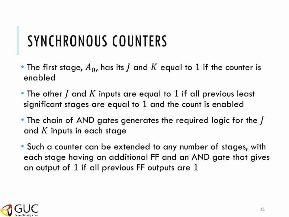
SYNCHRONOUS COUNTERS
11
• The first stage, 𝐴0, has its 𝐽 and 𝐾 equal to 1 if the counter is enabled
• The other 𝐽 and 𝐾 inputs are equal to 1 if all previous least significant stages are equal to 1 and the count is enabled
• The chain of AND gates generates the required logic for the 𝐽 and 𝐾 inputs in each stage
• Such a counter can be extended to any number of stages, with each stage having an additional FF and an AND gate that gives an output of 1 if all previous FF outputs are 1

12 𝐶𝑙𝑘
𝐴3
𝐴2
𝐴1
𝐴0
𝐶𝑜𝑢𝑛𝑡 𝑒𝑛𝑎𝑏𝑙𝑒 4 −BIT SYNCHRONOUS
BINARY COUNTER
𝑇𝑜 𝑛𝑒𝑥𝑡 𝑠𝑡𝑎𝑔𝑒
Is the polarity of the clock essential in this
design? What happens if we implement this
counter with a negative edge-triggered clock?
𝐽𝐾 𝐹𝐹 𝑐ℎ𝑎𝑟𝑎𝑐𝑡𝑒𝑟𝑖𝑠𝑡𝑖𝑐 𝑡𝑎𝑏𝑙𝑒
13
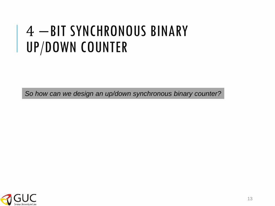
4 −BIT SYNCHRONOUS BINARY UP/DOWN COUNTER
So how can we design an up/down synchronous binary counter?

14 𝐶𝑙𝑘
𝐴3
𝐴2
𝐴1
𝐴0
𝑈𝑝
𝐷𝑜𝑤𝑛
𝐹𝑢𝑛𝑐𝑡𝑖𝑜𝑛 𝑡𝑎𝑏𝑙𝑒
𝑇 𝐹𝐹 𝑐ℎ𝑎𝑟𝑎𝑐𝑡𝑒𝑟𝑖𝑠𝑡𝑖𝑐 𝑡𝑎𝑏𝑙𝑒
This is not
a mistake!
With a mode control of
10 and a current count
of 0101, what is the
next count?
With a mode control of
01 and a current count
of 0111, what is the
next count?

UNUSED STATES
15
001
010
011
100
101
000 • What happens if we are interested in a counter design that does not include all states (counts)?
• For example, here is a state diagram and a state table (next slide) for a counter that repeatedly counts from 000 to 101
• What should we write in the table for the couple of unused states?

UNUSED STATES
16
001
010
011
100
101
000
Present State Next State
𝑸𝟐 𝑸𝟏 𝑸𝟎 𝑸𝟐 𝑸𝟏 𝑸𝟎
0 0 0 0 0 1
0 0 1 0 1 0
0 1 0 0 1 1
0 1 1 1 0 0
1 0 0 1 0 1
1 0 1 0 0 0
1 1 0 ? ? ?
1 1 1 ? ? ?
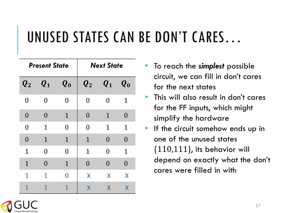
UNUSED STATES CAN BE DON’T CARES…
17
Present State Next State
𝑸𝟐 𝑸𝟏 𝑸𝟎 𝑸𝟐 𝑸𝟏 𝑸𝟎
0 0 0 0 0 1
0 0 1 0 1 0
0 1 0 0 1 1
0 1 1 1 0 0
1 0 0 1 0 1
1 0 1 0 0 0
1 1 0 X X X
1 1 1 X X X
• To reach the simplest possible
circuit, we can fill in don’t cares
for the next states
• This will also result in don’t cares
for the FF inputs, which might
simplify the hardware
• If the circuit somehow ends up in
one of the unused states
{110,111}, its behavior will
depend on exactly what the don’t
cares were filled in with

OR MAYBE WE DO CARE!
18
Present State Next State
𝑸𝟐 𝑸𝟏 𝑸𝟎 𝑸𝟐 𝑸𝟏 𝑸𝟎
0 0 0 0 0 1
0 0 1 0 1 0
0 1 0 0 1 1
0 1 1 1 0 0
1 0 0 1 0 1
1 0 1 0 0 0
1 1 0 0 0 0
1 1 1 0 0 0
• To reach the safest possible circuit,
we can explicitly fill in next states for
the unused states {110,111} • This guarantees that even if the
circuit somehow enters an unused
state, it will eventually end up into
one of the valid states
• This is called a self-starting counter
001
010
011
100
101
000
110 111

DESIGN PROBLEM
19
• Design a sequential logic circuit that implements the following recurring sequence:
000 → 010 → 011 → 100 → 101 → 111 → 000 → ⋯
Assume that the circuit is a self-starting one.

20
DESIGN PROBLEM: SOLUTION
1. From the word description and the required specifications, we sketch the state diagram. Since each state consists of 3 bits, we need 3 flip-flops 010
011
100
101
111
000
001 110
Here, 𝑇 FFs would be a good
choice, since we are going to
toggle some bits in every state
transition
21
DESIGN PROBLEM: SOLUTION
2. Next, we derive the state table. The present and next states are known from the state diagram. While the FF inputs are obtained with the help of the 𝑇 FF excitation table or characteristic equation
22
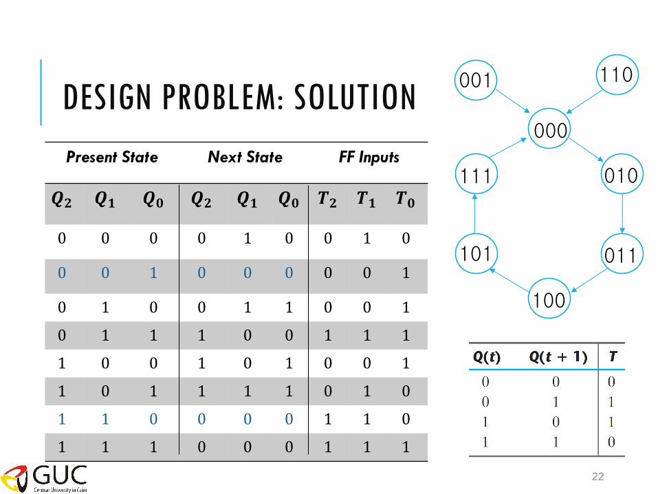
DESIGN PROBLEM: SOLUTION
010
011
100
101
111
000
001 110
Present State Next State FF Inputs
𝑸𝟐 𝑸𝟏 𝑸𝟎 𝑸𝟐 𝑸𝟏 𝑸𝟎 𝑻𝟐 𝑻𝟏 𝑻𝟎
0 0 0 0 1 0 0 1 0
0 0 1 0 0 0 0 0 1
0 1 0 0 1 1 0 0 1
0 1 1 1 0 0 1 1 1
1 0 0 1 0 1 0 0 1
1 0 1 1 1 1 0 1 0
1 1 0 0 0 0 1 1 0
1 1 1 0 0 0 1 1 1

23
DESIGN PROBLEM: SOLUTION
3. The FF input equations are then simplified
(carried out on the board)
4. Finally, the logic circuit of the counter is sketched
(carried out on the board)


