Embed Size (px)
Citation preview
IP: 5.10.31.210 On: Sat, 09 Jul 2022 21:18:04Copyright: American Scientific Publishers
Delivered by Ingenta
Copyright © 2019 American Scientific PublishersAll rights reservedPrinted in the United States of America
Journal ofLow Power ElectronicsVol. 15, 19–26, 2019
Low Power Flip-Flop Design Using Tri-State Inverter Logic
P. Indira1�∗ and M. Kamaraju21Department of Electronics & Communications Engineering, C.U. Shah University, Gujarat 363030, India
2Department of Electronics & Communications Engineering, JNT University, Gudlavalleru 521356, AndhraPradesh, India
(Received: 27 October 2018; Accepted: 18 January 2019)
Low power flip-flops are contributing to ‘Low power VLSI circuit design’ as flip-flops are the funda-mental storage blocks, which consume substantial amount of power. In this research, a low powerarea efficient dual edge implicit pulse-triggered flip-flop (LPAEFF) design is proposed with com-bined efforts of three models. The optimal clock gating is achieved by the MPSO algorithm, whichoptimizes the clock activity to reduce the power consumption. Tri-state inverter logic is used toreduce the delay. The MOSFET physics model optimally used to reduce the power and area. Thecombined efforts reduce the Power, Delay and PDP considerately. When compared to the existingflip-flop designs, our model achieves better experimental results in terms of Power, Delay, PDP, areaand other robust features. As the transistor count is reduced in this work, it gives an area efficientflip-flop design. This flip-flop design robustness tested at various PVT conditions. Particularly, withreference to the base counterpart (DIFF_CGS) flip-flop design, our model reduces Power by 22%;Delay by 65%; and PDP by 73% at 1.2 V, 65 nm and 25 �C. The proposed LPAEFF design wasimplemented with HSPICE and CAD tools.
Keywords: Low Power Area Efficient Flip-Flop (LPAEFF), Optimal Clock Gating, ModifiedParticle Swarm Optimization (MPSO), Complementary Metal-Oxide-Semiconductor(CMOS), Power Delay Product (PDP).
1. INTRODUCTIONCurrently, Low Power and High Performance are thehighly desirable design parameters in VLSI systemdesign.1 In order to achieve high performance (speed) indigital circuits, power saving is the main problem.2 Scalingdown reduces the power consumption, but it causes deteri-orating effects such as yielding and reliability problem, anincrease in leakage power, the occurrence of short channeleffects3 leading to circuit design vulnerable to failure.
Instead of reducing the supply voltage for power saving,application of power reduction schemes is more beneficial.One of such schemes is ‘dual edge triggering scheme.’4–6
Flip-flops are the basic storage blocks to support thepipelining technique to enhance the speed performance andthroughput. But, most of the power is consumed by flip-flops and clock distribution networks (about 30–60% ofthe total power used by these elements).7
Pulse triggered flip-flop has been considered as a popu-lar alternative to the conventional master-slave based flip-flop on higher-speed applications.8–10
∗Author to whom correspondence should be addressed.Email: [email protected]
There are two types of pulse triggered flip-flops whichare classified as implicit pulse generation and explicitpulse generation flip-flop. In general, Implicit pulse gener-ation is more power efficient because it merely controls thedischarge path, while Explicit pulse generation approachneeds to control the power by physically generatingTraining pulse.11
The explicit pulse triggered flip-flops are also usedin low power applications, such as DET-SAFF whichuses dual-edge triggering and conditional precharge inreducing the power.12 There are few other Low power,High performance flip-flops such as current mode logic(CML) D-flip-flop and low power pulse triggered flip-flop(LPPF) designs comes under this category.13�14 Currentmode D-flip-flops are based on negative differential resis-tance (NDR) phenomenon in which device count is min-imized. This improves the power and speed performanceof the flip-flop. Low power pulse flip-flop (LPPF) employsself driven pass transistor logic which reduces the power,maintains the speed without glitches and also reduces thepower delay product and they are suitable for high speedapplications.
J. Low Power Electron. 2019, Vol. 15, No. 1 1546-1998/2019/15/019/008 doi:10.1166/jolpe.2019.1586 19
IP: 5.10.31.210 On: Sat, 09 Jul 2022 21:18:04Copyright: American Scientific Publishers
Delivered by Ingenta
Low Power Flip-Flop Design Using Tri-State Inverter Logic Indira and Kamaraju
Conditional Data Mapping flip-flops (CDMFF), by map-ping their inputs through a configuration, eliminates redun-dant internal transitions to reduce the dynamic power.15
A clock-pseudo-NMOS level-converting flip-flop (CPN-LCFF) is an implicit pulse generating reduction schemewhich uses clocked-pseudo-NMOS technique and condi-tional discharge technique to reduce power, delay and PDPcompared to its counterparts.16
In Level shifting environment, another flip-flop whichis an implicit-pulsed Level Convert flip-flop (LCFF), usesclustered Voltage Scaling (CVS) technique that exhibitssmall delay and is suitable even to critical path also.17
A magnetic flip-flop (MFF) is a special category flip-flop that possesses the rich qualities of non-volatility, highsensing speed, easy interface to CMOS technology andabsolute power-off in ‘idle’ mode. TAS writing approachand PCSA sense amplifier bring high reliability to MFFand allow it to provide error-free output.18 Another implicitpulse triggered flip-flop design is Static Explicit-PulseDual-Edge Triggered flip-flop (SEDNIFF), in which latchnode kept inside the structure to reduce power, delay andPDP. It is a simple and robust model.19
In this paper, we propose a low power area efficientimplicit pulse dual edge triggered flip-flop (LPAEFF) tominimize Power, Delay and improve the Power DelayProduct.
2. PROBLEM METHODOLOGYAND SYSTEM MODEL
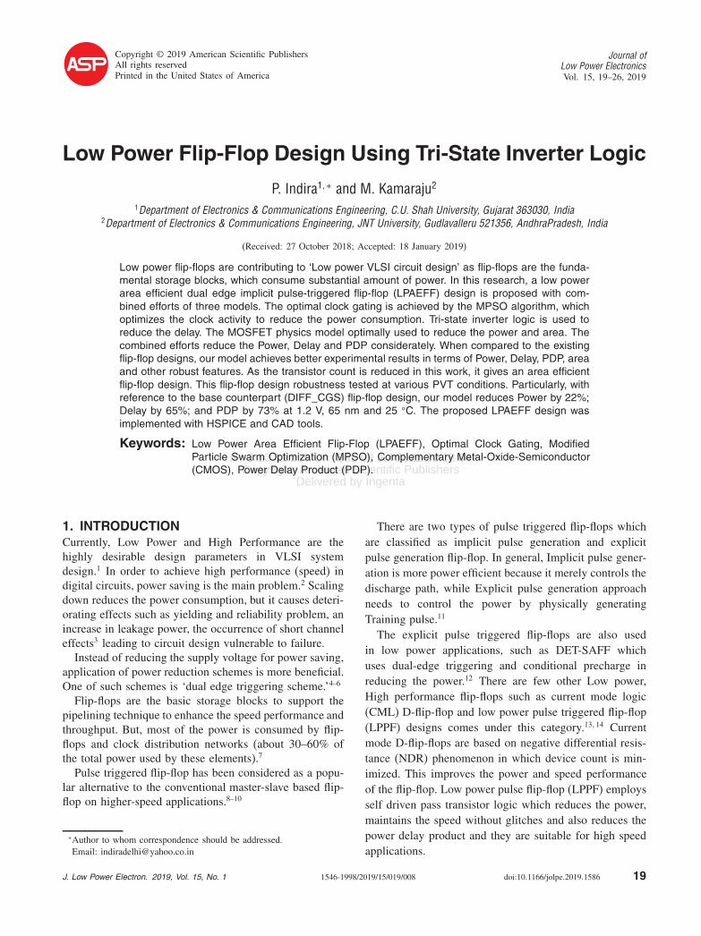
2.1. Problem MethodologyThe proposed model used three different techniques indi-vidually to contribute in reduction of power and delay, sothat power-delay-product can be reduced. Using the MOS-FET physics model, length and width of the channel canbe modified to reduce delay. The PVT awareness model isused in this work comprises various process technologieswith different supply voltages at different temperatures.By employing the Modified Particle Swarm Optimiza-
tion Algorithm, our proposed flip-flop design optimallyreduces the clock activity to reduce the dynamic power.The unwanted switching activity can be disabled at theidle time, without using any extra logic. In this, an optimalclock-gating technique can suppress the redundant tran-sitions of the clock with respect to the master clock todecrease the power.In this work, tri-state inverter logic contains 16 transis-
tors, whereas the counterpart DIFF-CGS flip-flop modelcontains 31 transistors and used extra logic to reduce thepower. In this manner, we propose a design which is morearea efficient. The tri-state inverter logic not only reducesthe power consumption, but also reduces the delay to ele-vate the model with low PDP when compared to the othermodels.
MOSFET physicsmodel
To design PMOS,NMOS transistors
To design LPAEFF
MPSO clock gating
Tri-state inverter logic
Perform post simulationusing HSPICE tool
Compute delay, power, andpower delay product
Fig. 1. Work flow of proposed design.
2.2. Work Flow and System Model ofProposed Design
The combined contributions of the proposed model givethe low power area efficient design as indicated inFigure 1.
3. PROPOSED LPAEFF DESIGNThe low power area efficient flip-Flop design using CMOSbulk process is proposed in this section. The proposeddesign consists of the combination of solutions that arebriefly discussed as follows.
3.1. MOSFET Physics ModelWe sized down the CMOS transistor by three times andchannel length reduced to half of the channel width in eachNMOS and PMOS transistor. Various device parameters(such as trans-conductance, output conductance, gain andunity gain cut-off frequency of the channel) are evaluatedfrom the transfer and output characteristics. The correla-tion among drain current, drain to source voltage, the gateto source voltage, and body to source voltage in variousregions of MOSFET operation in this model is describedbelow. In the strong inversion region, the drain currentequation in the linear region is given as follows:
Id = Id01
1+RdsId0(1)
where Id0 is the drain current without parasitic source-drain resistance effect. The Id0 represents as follows:
Id0 = ��Vgs−Vth−AbVds/2�Vds
1+ �Vds/EsL�(2)
where Vth is the threshold voltage, Es is the lateral electricfield at which the velocity saturates and Ab represents the
20 J. Low Power Electron. 15, 19–26, 2019

IP: 5.10.31.210 On: Sat, 09 Jul 2022 21:18:04Copyright: American Scientific Publishers
Delivered by Ingenta
Indira and Kamaraju Low Power Flip-Flop Design Using Tri-State Inverter Logic
account of the bulk charge effect. � is the basic parameterand represent by
�= �effCox
W
L(3)
Where �eff is the effective mobility, L is the channellength, W is the device channel width and Cox is the gatecapacitance per unit area. The drain current of the stronginversion region as follows:
Ids = �1�Vgs−Vth−AbVds�
(1+ Vds−Vds
Va
)(4)
where �1 represents the WCox, Vs, Vs is the saturationvelocity, Vds is the drain to source saturation velocity, andVa is the early voltage as follows:
Va =Ids
1+AbRds�1
+(1+ Pv
EsLeff
)(1Va�
+ 1Va�
)−1
(5)
Where Pv is the gate bias dependence of Va, and Va�, Va� isthe early voltage due to channel length modulation, draininduced barrier lowering (DIBL).
Va� =1P�
�Vgs−Vth−AbEsL��Vds−Vds�
AbEsL(6)
Va� =�Vgs−Vth+2Vt�
�1+P�Vbs�
(1− AbVds
AbVds+Vgs−Vth+2Vt
)(7)
The parameter P� , P� used to compensate the error causedin early voltage. The drain current of the sub-thresholdregion as follows:
Idst = �2�1− e�−Vds/Vt ��e�Vgs−Vth−Voff �/SthVt (8)
Where Voff is the offset voltage, Sth is the sub-thresholdswing, and �2 as follows,
�2 = �0
W
L
√qsNch
s
V 2t (9)
where �0 is the bulk carrier mobility, qs is the permittivityof the semiconductor, Nch is the doping concentration, ands is the surface potential. The sub-threshold swing is afunction of channel length and the interface trapped-chargedensity and modeled as follows:
Sth = 1+Ec
Cd
Ccox
+Ccd
+ ��Cdsc+CdscdVds+CdscbVbs�e−c1�Leff/2Lt�+2e−c1�Leff/Lt��
Cox
(10)
Where Cd is the depletion capacitance, Cdsc, Cdscd, andCdscb is the channel coupling capacitance Ccd is the capac-itance due to interface trapped-charge density and theparameter Ec used to compensate the errors in the deple-tion width capacitance Leff is the effective channel length
and C1 is the first coefficient of short channel effects onthe threshold voltage. The threshold voltage of this modelrepresent as follows:
VTH = Vthl+
(K1
√1+2f +s+
NL
Leff
−Vbs−K2Vbs
+ �K3+K3bVbs�Tox
Weff +W0
2f
−4SthVds
(Vbi −2f
Vds
− �E1+E2�Vbs
))(11)
where K1 and K2 are the first order and second order bodyeffect coefficients, K3 is the narrow width, K3b is the bodyeffect coefficient, W0 is the narrow width parameter, Tox isthe gate oxide thickness, Leff and Weff are the effective-channel length and effective width of the device, and Vthl isthe threshold voltage for long channel MOSFET at Vds =50 mV and Vbs = 0. The is +1 for N-channel and −1 forP-channel MOSFETs. This model assumes that the mobil-ity is independent of Vds and hence the lateral electric field.The unified formulation of effective mobility defined asfollows:
�eff = �1
1+��2��Vgs+Vth�/tox�+�3��Vgs+Vth�/tox�2��1+�4Vbs�
(12)where �1 is the low-field mobility, �2 and �3 are the firstand second order mobility degradation coefficients, respec-tively, and �4 is a mobility degradation coefficient due tothe body effect.The depletion width becomes non-uniform along the
channel in a long channel MOSFET particularly when thedrain bias is high. This phenomenon, also termed as bulkcharge effect, causes Vth to vary along the channel. Thebulk effect Ab is given as follows:
Ab = 1+Ab1�x1Ab2−x2Ab3+Ab4��1
1+KETAVbs
(13)
where, Ab1 = K1/2√2f −Vbs, Ab2 = 1, Ab3 =
Ags�Vgs−Vth��Leff/�Leff +2√Jdep��
2, x1 = x2 = A0Leff/
�Leff +2√Jdep�, and Ab4 = B0/�Weff +B1�.
Where A0 is the bulk charge effect coefficient for chan-nel length, B0, B1 are the bulk charge effect coefficientsfor channel width, and it’s offset respectively, Jdep is thesource/drain junction depletion thickness in the channelregion, Ags is the gate bias coefficient and KETA is thebody-bias coefficient of bulk charge effect. The computedparameters are applied in a conventional MOSFET design.
3.2. PSO Based Clock Gating Methodology [20]Particle Swarm Optimization (PSO) is a search, HeuristicAlgorithm. It is used to obtain optimized Results. Thiscomputational technique, connected to Swarm of particles,which move in the global space in search of their goal
J. Low Power Electron. 15, 19–26, 2019 21
IP: 5.10.31.210 On: Sat, 09 Jul 2022 21:18:04Copyright: American Scientific Publishers
Delivered by Ingenta
Low Power Flip-Flop Design Using Tri-State Inverter Logic Indira and Kamaraju
(the place which best suits their needs) is given by a fitnessfunction below.All particles share information, any particle knows what
is the best position ever visited by any other particlein the Swarm. That best position is called Global bestposition �g�t��.Even though many variations exist, all particles
attain their better positions compared to their previ-ous positions. Those positions are termed as “local bestpositions” �Pi�t��.Each particle has a position and a velocity vectors which
are calculated as follows:
Xi�t+1�= Xi�t�+Vi�t+1� (14)
Vi�t+1�=WVi�t�+C1�Pi�t�−Xi�t��+C2�g�t�−Xi�t��(15)
We are using the PSO algorithm in our work to optimizethe clock input.In the proposed MPSO (Modified Particle Swarm Opti-
mization) algorithm, clock input (clk) and circuit out-put (Q) are considered in place of position and velocityvectors in PSO.Input clock position and corresponding output can be
calculated with a fitness function for every local best posi-tion. The delay gets reduced by taking the feedback fromthe output.Fitness function:
F �x�=(x1
dpn
Cpn
)+(x2
Eavg
Emax
)+(x3
1Cpn
)(16)
UQ =WQin−1+W1�pclkin − clkin−1
�+W2�gclkin − clkin−1�
(17)Uclk = clkin−1
+UQ (18)
After giving input clk and output Q, the delay of clkcomputes the exact place of control activation signal Cs
(enable signal); then Cs as one input and clk as anotherinput to MPSO gives a modified clock, so that it reducesthe total compute time in obtaining the output.
Algorithm 1 (Clock Gating Using MPSO).Input: Clk // Clock inputQ //flip-flop outputCs//Control activation signalOutput:Mclk//Optimal clock1. for each Clk2. initialize Clk ( )3. end for4. for each Clk do5. calculate fitness ( )6. if the current fitness is better than Pbest
7. set new Pbest = current best8. End9. for each Clk do
10. calculate dpm, Cpm, Eavg, Emax
11. calculate Q12. update the new Pbest using Eqs. (17) and (18)Return: Mclk //modified clock
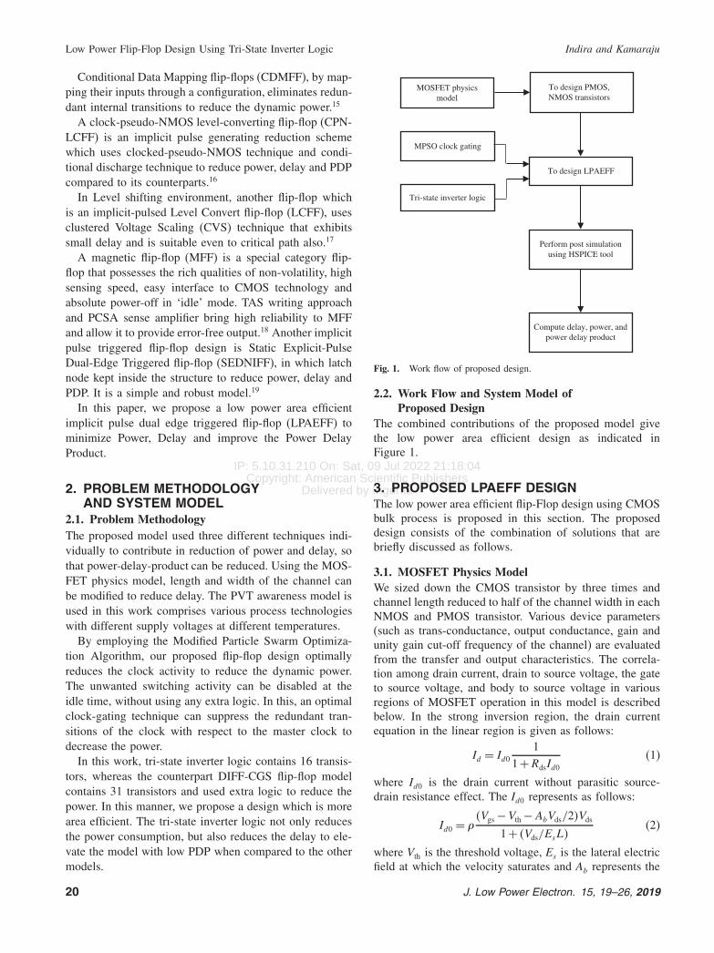
3.3. LPAEFF Design Using Tri-State Inverter LogicThe tri-state inverter is a digital circuit that produces threetypes of outputs: either ‘1’ or ‘0’ or ‘High Impedancestate.’ In “High Impedance state” the digital circuit out-put electronically gets disconnected as shown in Figure 2.This state is called as an ‘open-circuited’ state.In the other case, the output corresponds to the inverted
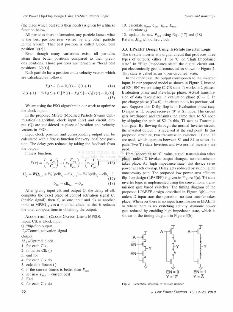
input. In our proposed model as shown in Figure 3, insteadof EN, EN′ we are using C, CB state. It works in 2 phases:Evaluation phase and Pre-charge phase. Actual transmis-sion of data takes place in evaluation phase (C = 1). Inpre-charge phase (C= 0), the circuit holds its previous val-ues. Suppose this D flip-flop is in Evaluation phase (say,D input is 1), output receives ‘0’ at S1 node. The circuitgets overlapped and transmits the same data to S3 nodeby skipping the path of S2. In this, T1 acts as Transmis-sion gate. By flowing through the normal Inverter circuit,the inverted output 1 is received at the end point. In thisproposed structure, two transmission switches T1 and T2are used, which operates between S1 and S4 to select thepath. Two Tri-state Inverters and two normal inverters areused.Here, according to ‘C’ value, signal transmission takes
place; unless D invokes output changes, no transmissiontakes place. At ‘high impedance state’ this device savespower at each overlap. Delay gets reduced by skipping theunnecessary path. The proposed low power area efficientflip-flop design (LPAEFF) is given in Figure 3(a). Tri-stateinverter logic is implemented using the conventional trans-mission gate based switches. The timing diagram of theproposed LPAEFF design described in Figure 3(b)—thatunless D input start the operation, no data transfer takesplace. Whenever there is no input transmission in LPAEFF,or where there is no switching activity, dynamic powergets reduced by enabling high impedance state, which isshown in the timing diagram in Figure 3(b).
Fig. 2. Schematic structure of tri-state inverter.
22 J. Low Power Electron. 15, 19–26, 2019
IP: 5.10.31.210 On: Sat, 09 Jul 2022 21:18:04Copyright: American Scientific Publishers
Delivered by Ingenta
Indira and Kamaraju Low Power Flip-Flop Design Using Tri-State Inverter Logic
(a)
C
C
D
Q
Q
(b)
Fig. 3. Proposed LPAEFF with tri-state inverter (a) schematic structure (b) timing diagram.
4. SYSTEM PERFORMANCEThe performance of the proposed LPAEFF designis deeply analyzed with different CMOS technologies(45 nm, 65 nm and 90 nm). CAD simulations were carriedout through HSPICE tool with different supply voltages.
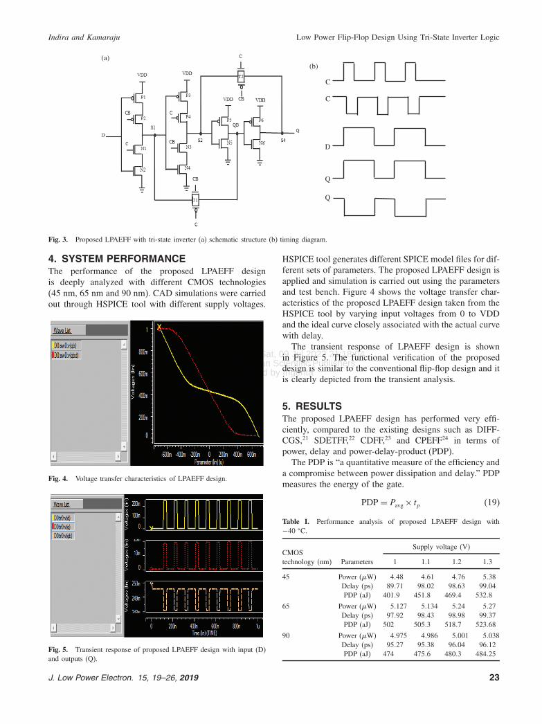
Fig. 4. Voltage transfer characteristics of LPAEFF design.
Fig. 5. Transient response of proposed LPAEFF design with input (D)and outputs (Q).
HSPICE tool generates different SPICE model files for dif-ferent sets of parameters. The proposed LPAEFF design isapplied and simulation is carried out using the parametersand test bench. Figure 4 shows the voltage transfer char-acteristics of the proposed LPAEFF design taken from theHSPICE tool by varying input voltages from 0 to VDDand the ideal curve closely associated with the actual curvewith delay.The transient response of LPAEFF design is shown
in Figure 5. The functional verification of the proposeddesign is similar to the conventional flip-flop design and itis clearly depicted from the transient analysis.
5. RESULTSThe proposed LPAEFF design has performed very effi-ciently, compared to the existing designs such as DIFF-CGS,21 SDETFF,22 CDFF,23 and CPEFF24 in terms ofpower, delay and power-delay-product (PDP).The PDP is “a quantitative measure of the efficiency and
a compromise between power dissipation and delay.” PDPmeasures the energy of the gate.
PDP = Pavg× tp (19)
Table I. Performance analysis of proposed LPAEFF design with−40 �C.
Supply voltage (V)CMOStechnology (nm) Parameters 1 1.1 1.2 1.3
45 Power (�W) 4�48 4�61 4�76 5�38Delay (ps) 89�71 98�02 98�63 99�04PDP (aJ) 401�9 451�8 469�4 532�8
65 Power (�W) 5�127 5�134 5�24 5�27Delay (ps) 97�92 98�43 98�98 99�37PDP (aJ) 502 505�3 518�7 523�68
90 Power (�W) 4�975 4�986 5�001 5�038Delay (ps) 95�27 95�38 96�04 96�12PDP (aJ) 474 475�6 480�3 484�25
J. Low Power Electron. 15, 19–26, 2019 23
IP: 5.10.31.210 On: Sat, 09 Jul 2022 21:18:04Copyright: American Scientific Publishers
Delivered by Ingenta
Low Power Flip-Flop Design Using Tri-State Inverter Logic Indira and Kamaraju
Table II. Performance analysis of proposed LPAEFF design with 25 �C.
Supply voltage (V)CMOStechnology (nm) Parameters 1 1.1 1.2 1.3
45 Power (�W) 5�62 5�82 6�13 6�26Delay (ps) 104�8 110�8 114�9 119�1PDP (aJ) 589 644�6 704�33 745�57
65 Power (�W) 5�27 5�41 5�48 5�56Delay (ps) 97�99 98�99 99�12 99�97PDP (aJ) 516�4 535�5 543�17 555�83
90 Power (�W) 5�05 5�43 5�57 5�64Delay (ps) 95�75 96�98 97�15 97�89PDP (aJ) 483�5 526�6 541�12 552�1
Table III. Performance analysis of proposed LPAEFF design with125 �C.
Supply voltage (V)CMOStechnology (nm) Parameters 1 1.1 1.2 1.3
45 Power (�W) 6�02 6�12 6�12 6�42Delay (ps) 130�1 145�3 142�9 150�23PDP (aJ) 783�1 889�2 874�6 964�48
65 Power (�W) 5�74 5�97 6�21 6�4Delay (ps) 127 132�1 141�3 149�78PDP (aJ) 728�9 788�6 877�5 958�6
90 Power (�W) 5�1 5�35 6�01 6�23Delay (ps) 125 128 135�7 143�12PDP (aJ) 637�5 684�8 815�9 891�64
PDP stands for the Average energy consumed per switch-ing activity. The design goal is to minimize the PDP inorder to get low power in high frequencies. At high fre-quencies, power dissipation is governed by capacitive load.Hence, we considered less capacitive load carefully. Inother words, without compromising with the speed, weachieved the reduction in power and delay. Propagationdelay is measured for both rise tplh and fall tphl outputtransitions.
tp =tplh+ tphl
2(20)
Propagation delay (tp� is the difference between the timerequired for the input to reach its 50% voltage level andthe time required to reach its 50% output voltage level.The proposed LPAEFF design has used different CMOS
technologies such as 45, 65, 90 nm with different supply
Table IV. Performance comparison of proposed and existing flip-flops(1.2 V; 65 nm; 25 �C).
Parameters
FF name Delay (ps) Power (�W) PDP (aJ)
SDETFF 166�39 15�153 2443�9CDFF 188�44 16�158 2934�8CPEFF 177�72 11�998 2014�8DIFF-CGS 286�21 7�044 1982�6LPAEFF 99�12 5�48 543�17
0
1000
2000
3000
4000
SDETFF CDFF CPEFF DIFF-CGS LPAEFF
PD
P (
aJ)
Flip-flop designs
PDP comparison of different flip-flops
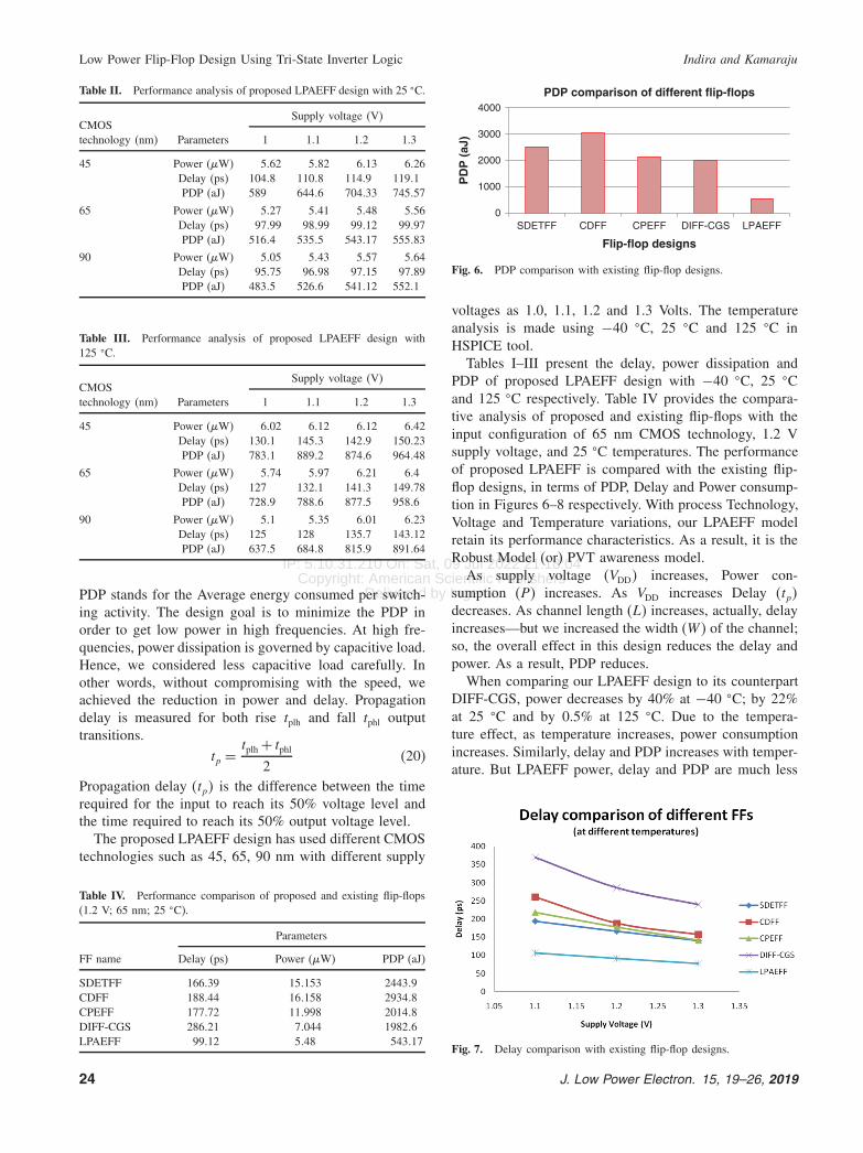
Fig. 6. PDP comparison with existing flip-flop designs.
voltages as 1.0, 1.1, 1.2 and 1.3 Volts. The temperatureanalysis is made using −40 �C, 25 �C and 125 �C inHSPICE tool.Tables I–III present the delay, power dissipation and
PDP of proposed LPAEFF design with −40 �C, 25 �Cand 125 �C respectively. Table IV provides the compara-tive analysis of proposed and existing flip-flops with theinput configuration of 65 nm CMOS technology, 1.2 Vsupply voltage, and 25 �C temperatures. The performanceof proposed LPAEFF is compared with the existing flip-flop designs, in terms of PDP, Delay and Power consump-tion in Figures 6–8 respectively. With process Technology,Voltage and Temperature variations, our LPAEFF modelretain its performance characteristics. As a result, it is theRobust Model (or) PVT awareness model.As supply voltage (VDD� increases, Power con-
sumption (P ) increases. As VDD increases Delay (tp�decreases. As channel length (L) increases, actually, delayincreases—but we increased the width (W ) of the channel;so, the overall effect in this design reduces the delay andpower. As a result, PDP reduces.When comparing our LPAEFF design to its counterpart
DIFF-CGS, power decreases by 40% at −40 �C; by 22%at 25 �C and by 0.5% at 125 �C. Due to the tempera-ture effect, as temperature increases, power consumptionincreases. Similarly, delay and PDP increases with temper-ature. But LPAEFF power, delay and PDP are much less
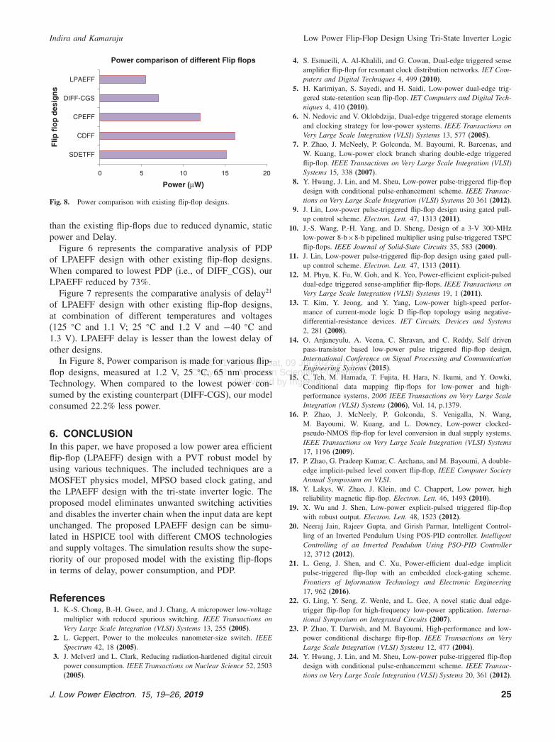
Fig. 7. Delay comparison with existing flip-flop designs.
24 J. Low Power Electron. 15, 19–26, 2019
IP: 5.10.31.210 On: Sat, 09 Jul 2022 21:18:04Copyright: American Scientific Publishers
Delivered by Ingenta
Indira and Kamaraju Low Power Flip-Flop Design Using Tri-State Inverter Logic
0 5 10 15 20
SDETFF
CDFF
CPEFF
DIFF-CGS
LPAEFF
Power (µW)
Flip
flo
p d
esig
ns
Power comparison of different Flip flops
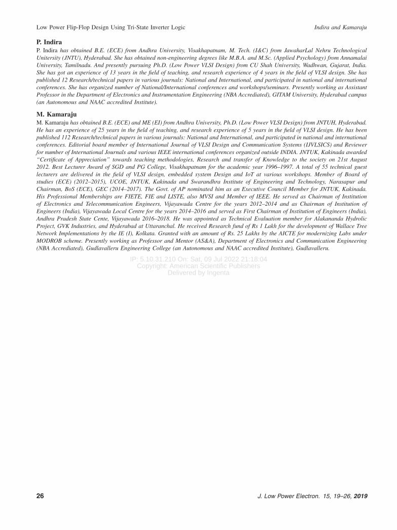
Fig. 8. Power comparison with existing flip-flop designs.
than the existing flip-flops due to reduced dynamic, staticpower and Delay.
Figure 6 represents the comparative analysis of PDPof LPAEFF design with other existing flip-flop designs.When compared to lowest PDP (i.e., of DIFF_CGS), ourLPAEFF reduced by 73%.
Figure 7 represents the comparative analysis of delay21
of LPAEFF design with other existing flip-flop designs,at combination of different temperatures and voltages(125 �C and 1.1 V; 25 �C and 1.2 V and −40 �C and1.3 V). LPAEFF delay is lesser than the lowest delay ofother designs.
In Figure 8, Power comparison is made for various flip-flop designs, measured at 1.2 V, 25 �C, 65 nm processTechnology. When compared to the lowest power con-sumed by the existing counterpart (DIFF-CGS), our modelconsumed 22.2% less power.
6. CONCLUSIONIn this paper, we have proposed a low power area efficientflip-flop (LPAEFF) design with a PVT robust model byusing various techniques. The included techniques are aMOSFET physics model, MPSO based clock gating, andthe LPAEFF design with the tri-state inverter logic. Theproposed model eliminates unwanted switching activitiesand disables the inverter chain when the input data are keptunchanged. The proposed LPAEFF design can be simu-lated in HSPICE tool with different CMOS technologiesand supply voltages. The simulation results show the supe-riority of our proposed model with the existing flip-flopsin terms of delay, power consumption, and PDP.
References1. K.-S. Chong, B.-H. Gwee, and J. Chang, A micropower low-voltage
multiplier with reduced spurious switching. IEEE Transactions onVery Large Scale Integration (VLSI) Systems 13, 255 (2005).
2. L. Geppert, Power to the molecules nanometer-size switch. IEEESpectrum 42, 18 (2005).
3. J. McIverJ and L. Clark, Reducing radiation-hardened digital circuitpower consumption. IEEE Transactions on Nuclear Science 52, 2503(2005).
4. S. Esmaeili, A. Al-Khalili, and G. Cowan, Dual-edge triggered senseamplifier flip-flop for resonant clock distribution networks. IET Com-puters and Digital Techniques 4, 499 (2010).
5. H. Karimiyan, S. Sayedi, and H. Saidi, Low-power dual-edge trig-gered state-retention scan flip-flop. IET Computers and Digital Tech-niques 4, 410 (2010).
6. N. Nedovic and V. Oklobdzija, Dual-edge triggered storage elementsand clocking strategy for low-power systems. IEEE Transactions onVery Large Scale Integration (VLSI) Systems 13, 577 (2005).
7. P. Zhao, J. McNeely, P. Golconda, M. Bayoumi, R. Barcenas, andW. Kuang, Low-power clock branch sharing double-edge triggeredflip-flop. IEEE Transactions on Very Large Scale Integration (VLSI)Systems 15, 338 (2007).
8. Y. Hwang, J. Lin, and M. Sheu, Low-power pulse-triggered flip-flopdesign with conditional pulse-enhancement scheme. IEEE Transac-tions on Very Large Scale Integration (VLSI) Systems 20 361 (2012).
9. J. Lin, Low-power pulse-triggered flip-flop design using gated pull-up control scheme. Electron. Lett. 47, 1313 (2011).
10. J.-S. Wang, P.-H. Yang, and D. Sheng, Design of a 3-V 300-MHzlow-power 8-b×8-b pipelined multiplier using pulse-triggered TSPCflip-flops. IEEE Journal of Solid-State Circuits 35, 583 (2000).
11. J. Lin, Low-power pulse-triggered flip-flop design using gated pull-up control scheme. Electron. Lett. 47, 1313 (2011).
12. M. Phyu, K. Fu, W. Goh, and K. Yeo, Power-efficient explicit-pulseddual-edge triggered sense-amplifier flip-flops. IEEE Transactions onVery Large Scale Integration (VLSI) Systems 19, 1 (2011).
13. T. Kim, Y. Jeong, and Y. Yang, Low-power high-speed perfor-mance of current-mode logic D flip-flop topology using negative-differential-resistance devices. IET Circuits, Devices and Systems2, 281 (2008).
14. O. Anjaneyulu, A. Veena, C. Shravan, and C. Reddy, Self drivenpass-transistor based low-power pulse triggered flip-flop design,International Conference on Signal Processing and CommunicationEngineering Systems (2015).
15. C. Teh, M. Hamada, T. Fujita, H. Hara, N. Ikumi, and Y. Oowki,Conditional data mapping flip-flops for low-power and high-performance systems, 2006 IEEE Transactions on Very Large ScaleIntegration (VLSI) Systems (2006), Vol. 14, p.1379.
16. P. Zhao, J. McNeely, P. Golconda, S. Venigalla, N. Wang,M. Bayoumi, W. Kuang, and L. Downey, Low-power clocked-pseudo-NMOS flip-flop for level conversion in dual supply systems.IEEE Transactions on Very Large Scale Integration (VLSI) Systems17, 1196 (2009).
17. P. Zhao, G. Pradeep Kumar, C. Archana, and M. Bayoumi, A double-edge implicit-pulsed level convert flip-flop, IEEE Computer SocietyAnnual Symposium on VLSI.
18. Y. Lakys, W. Zhao, J. Klein, and C. Chappert, Low power, highreliability magnetic flip-flop. Electron. Lett. 46, 1493 (2010).
19. X. Wu and J. Shen, Low-power explicit-pulsed triggered flip-flopwith robust output. Electron. Lett. 48, 1523 (2012).
20. Neeraj Jain, Rajeev Gupta, and Girish Parmar, Intelligent Control-ling of an Inverted Pendulum Using POS-PID controller. IntelligentControlling of an Inverted Pendulum Using PSO-PID Controller12, 3712 (2012).
21. L. Geng, J. Shen, and C. Xu, Power-efficient dual-edge implicitpulse-triggered flip-flop with an embedded clock-gating scheme.Frontiers of Information Technology and Electronic Engineering17, 962 (2016).
22. G. Ling, Y. Seng, Z. Wenle, and L. Gee, A novel static dual edge-trigger flip-flop for high-frequency low-power application. Interna-tional Symposium on Integrated Circuits (2007).
23. P. Zhao, T. Darwish, and M. Bayoumi, High-performance and low-power conditional discharge flip-flop. IEEE Transactions on VeryLarge Scale Integration (VLSI) Systems 12, 477 (2004).
24. Y. Hwang, J. Lin, and M. Sheu, Low-power pulse-triggered flip-flopdesign with conditional pulse-enhancement scheme. IEEE Transac-tions on Very Large Scale Integration (VLSI) Systems 20, 361 (2012).
J. Low Power Electron. 15, 19–26, 2019 25
IP: 5.10.31.210 On: Sat, 09 Jul 2022 21:18:04Copyright: American Scientific Publishers
Delivered by Ingenta
Low Power Flip-Flop Design Using Tri-State Inverter Logic Indira and Kamaraju
P. IndiraP. Indira has obtained B.E. (ECE) from Andhra University, Visakhapatnam, M. Tech. (I&C) from JawaharLal Nehru TechnologicalUnitersity (JNTU), Hyderabad. She has obtained non-engineering degrees like M.B.A. and M.Sc. (Applied Psychology) from AnnamalaiUniversity, Tamilnadu. And presently pursuing Ph.D. (Low Power VLSI Design) from CU Shah University, Wadhwan, Gujarat, India.She has got an experience of 13 years in the field of teaching, and research experience of 4 years in the field of VLSI design. She haspublished 12 Research/technical papers in various journals: National and International, and participated in national and internationalconferences. She has organized number of National/International conferences and workshops/seminars. Presently working as AssistantProfessor in the Department of Electronics and Instrumentation Engineering (NBA Accrediated), GITAM University, Hyderabad campus(an Autonomous and NAAC accredited Institute).
M. KamarajuM. Kamaraju has obtained B.E. (ECE) and ME (EI) from Andhra University, Ph.D. (Low Power VLSI Design) from JNTUH, Hyderabad.He has an experience of 25 years in the field of teaching, and research experience of 5 years in the field of VLSI design. He has beenpublished 112 Research/technical papers in various journals: National and International, and participated in national and internationalconferences. Editorial board member of International Journal of VLSI Design and Communication Systems (IJVLSICS) and Reviewerfor number of International Journals and various IEEE international conferences organized outside INDIA. JNTUK, Kakinada awarded“Certificate of Appreciation” towards teaching methodologies, Research and transfer of Knowledge to the society on 21st August2012. Best Lecturer Award of SGD and PG College, Visakhapatnam for the academic year 1996–1997. A total of 55 technical guestlecturers are delivered in the field of VLSI design, embedded system Design and IoT at various workshops. Member of Board ofstudies (ECE) (2012–2015), UCOE, JNTUK, Kakinada and Swarandhra Institute of Engineering and Technology, Narasapur andChairman, BoS (ECE), GEC (2014–2017). The Govt. of AP nominated him as an Executive Council Member for JNTUK, Kakinada.His Professional Memberships are FIETE, FIE and LISTE, also MVSI and Member of IEEE. He served as Chairman of Institutionof Electronics and Telecommunication Engineers, Vijayawada Centre for the years 2012–2014 and as Chairman of Institution ofEngineers (India), Vijayawada Local Centre for the years 2014–2016 and served as First Chairman of Institution of Engineers (India),Andhra Pradesh State Cente, Vijayawada 2016–2018. He was appointed as Technical Evaluation member for Alakananda HydrolicProject, GVK Industries, and Hyderabad at Uttaranchal. He received Research fund of Rs 1 Lakh for the development of Wallace TreeNetwork Implementations by the IE (I), Kolkata. Granted with an amount of Rs. 25 Lakhs by the AICTE for modernizing Labs underMODROB scheme. Presently working as Professor and Mentor (AS&A), Department of Electronics and Communication Engineering(NBA Accrediated), Gudlavalleru Engineering College (an Autonomous and NAAC accredited Institute), Gudlavalleru.
26 J. Low Power Electron. 15, 19–26, 2019


