Embed Size (px)
Citation preview
1142 IEEE TRANSACTIONS ON POWER ELECTRONICS, VOL. 21, NO. 4, JULY 2006
Realization of Parasitics in State-Space Average-ValueModeling of PWM DC–DC Converters
Ali Davoudi, Student Member, IEEE, and Juri Jatskevich, Member, IEEE
Abstract—Analytical average-value modeling of pulsewidthmodulation dc–dc converters is usually based on the piece-wiselinear waveforms of the circuit variables and neglects the par-asitics that give rise to waveform nonlinearities and complicatemodel derivation. This letter presents a straightforward but pow-erful methodology that considers the true averaging of nonlinearwaveforms and produces a fairly accurate large-signal transientmodel that is functional in both operational modes. Based onthe proposed modeling approach, a fast procedure for extractingthe small-signal frequency-domain characteristics is set forth.The key model parameters are established numerically using thedetailed simulation, which streamlines the analysis. The resultingaverage-value model is validated with a hardware prototype, adetailed simulation, and several previously established models intime and frequency domains.
Index Terms—Average-value modeling, parasitics, pulsewidthmodulation (PWM) dc–dc converters, state-space averaging(SSA).
I. INTRODUCTION
AVERAGE-VALUE modeling of basic dc–dc converters isoften performed by averaging the switching cell/network,
known as circuit averaging (CA), or by averaging the corre-sponding state-space equations, known as state-space averaging(SSA). As averaging methods evolved for discontinuous con-duction mode (DCM), reduced-order, full-order, and correctedfull-order models have been introduced [1] that assume idealcomponents and piecewise linear waveforms of the circuit vari-ables (linear ripple approximation [2], [3]).
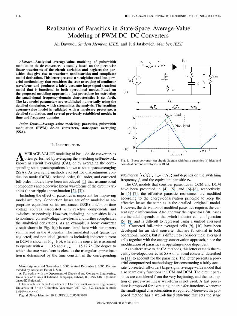
Including the effect of parasitics is important for improvingmodel accuracy. Conduction losses are often modeled as ap-propriate equivalent series resistances (ESR) and/or on-timevoltage sources associated with reactive components andswitches, respectively. However, including the parasitics leadsto nonlinear current/voltage waveforms and further complicatesthe analytical derivations. As an example, a boost convertercircuit shown in Fig. 1(a) is considered here with parameterssummarized in the Appendix. The simulated ideal (parasiticsneglected) and non-ideal (parasitics included) inductor currentin DCM is shown in Fig. 1(b), wherein the converter is assumedto operate with 0.5 and 15.12 . The degree towhich the true waveform is close to the triangular approxima-tion is determined by the time constant in the corresponding
Manuscript received November 3, 2005; revised December 2, 2005. Recom-mended by Associate Editor J. Sun.
A. Davoudi is with the Department of Electrical and Computer Engineering,University of Illinois at Urbana-Champaign, Urbana, IL, USA 61801 (e-mail:[email protected]).
J. Jatskevich is with the Department of Electrical and Computer Engineering,University of British Columbia, Vancouver V6T 1Z4, BC, Canada (e-mail:[email protected]).
Digital Object Identifier 10.1109/TPEL.2006.879048
Fig. 1. Boost converter: (a) circuit diagram with basic parasitics (b) ideal andnon-ideal current waveforms in DCM.
subinterval and depends on the switchingfrequency and the equivalent parasitic .
The CA models that consider parasitics in CCM and DCMhave been presented in [4], [5], and [6]–[8], respectively.In [5]–[7], the effective parasitic resistances are modifiedaccording to the energy-conservation principle to keep theeffective losses the same as in the detailed “original” model.However, the derivation of modified parasitics requires the cur-rent ripple information. Also, the way the capacitor ESR lossesare included depends on the switch-inductor-cell configuration[5], [8] and is difficult to represent using a unified averagedcell. Corrected full-order averaged cells [9], [10] have beendeveloped for an ideal converter that are functional in bothoperational modes, but it is difficult to consider these averagedcells together with the energy-conservation approach, since themodification of parasitics is operating-mode dependent.
As an alternative to the CA methods, this letter extends the re-cently developed corrected SSA of an ideal converter describedin [11] to account for the parasitics. The letter presents a pow-erful computerized methodology for constructing a fairly accu-rate (corrected full-order) large-signal average-value model thatalso seamlessly functions in CCM and DCM. The circuit para-sitics are considered from the very beginning, and the assump-tion of piece-wise linear waveform is not used. A fast proce-dure is proposed for extracting the transfer-functions wheneverthe small-signal characterization is required. Moreover, the pro-posed method has a well-defined structure that sets the stage
0885-8993/$20.00 © 2006 IEEE
IEEE TRANSACTIONS ON POWER ELECTRONICS, VOL. 21, NO. 4, JULY 2006 1143
both for further automating the construction of accurate aver-aged models and avoiding laborious analytical derivations.
II. CONSIDERING PARASITICS IN STATE-SPACE AVERAGING
A. State-Space Averaged Model of an Ideal Converter
The state-space averaging method involves the weightedsum of the state-space equations corresponding to the differentsubintervals depicted in Fig. 1(b), wherein the DCM of inductorcurrent is assumed. To accurately represent the converter dy-namics, a corrected full-order state-space averaged model [11]has been recently proposed for an ideal converter as
(1)
where the corresponding state vector is denoted by. The bar symbol is used to denote the so-called fast
average (or the true average) of a state variable over aprototypical switching interval
(2)
The so-called correction matrix is added in (1) to make theconventional state-space averaging work properly in DCM. Foran ideal topology (without parasitics), the inductor current isassumed to have a triangular waveform, as shown in Fig. 1(b)(dashed-line), for which case the diagonal correction matrixis found to be
(3)
where the duty cycle is determined externally [11]. Thesecond subinterval , also known as the duty-ratio-constraint[11], becomes algebraically dependent on other system vari-ables and has been found in corrected full-order models, whichassume a piece-wise linear inductor current [1], [4], [7], [9],[11], [12].
B. Including the Parasitics
Since (3) was derived for the triangular waveform, it isno longer accurate when the parasitics are considered. Al-ternatively, this letter proposes a new method of correctingthe averaged state-space equation that is valid no matter howlarge or small the parasitics. To better understand how theparasitics can be included, it is instructive to partition withinthe switching interval in terms of individual subintervals as
elsewhere(4)
elsewhere(5)
elsewhere(6)
such that . The corresponding local state modelsare
elsewhere(7)
elsewhere(8)
elsewhere(9)
Applying (2) to both sides of (7)–(9) produces
(10)
The final averaged system-equation is obtained from (10) as
(11)
which includes the parasitics in the state-space matrices and iscorrect, regardless of the ripple size and/or the waveform non-linearity of . Moreover, the averaged state vector may bepulled out of the summation and (11) can be rewritten as
(12)
where the diagonal weighing-correction matrices arewith the entries defined as
(13)
with 0 due to DCM.If the parasitics and the capacitor dynamics are neglected and
a triangular current waveform (see Fig. 1(b)-dashed line) is as-sumed as in [11], then the local averages are related to the idealpeak value of the current and the overall average as
(14)
from which it follows that
(15)
Moreover, because the derivative of in the third subintervalis zero, the corresponding entries of and also have zeros.Therefore, could be any non-zero number that would mul-tiply with the first row of and give zero as a final result. Then,one can set to be
(16)
1144 IEEE TRANSACTIONS ON POWER ELECTRONICS, VOL. 21, NO. 4, JULY 2006
If the capacitor voltage ripple is neglected and is assumedconstant, then
(17)
Based on (15)–(17), it is possible to pull the matricesoutside of the summation in (12) and express the correctedstate-space averaged equation as (1) with the correction matrixdefined by (3).
However, in the presence of parasitics, (14) is not true. Con-sequently, (15) and (16) are no longer valid. Moreover, due tothe inevitable ripple in , (17) is also not true. As a result of re-moving the assumptions of piece-wise linear current and voltagewaveforms, instead of (3), the true correction matrix becomes
(18)
which is very difficult to evaluate analytically. Alternatively, themethodology described in this letter makes use of the diagonalcorrection matrices and the corrected state-space equation(12).
In DCM, becomes algebraically dependent on other vari-ables. To provide an accurate model, the duty ratio constraintmust be modified to include the effect of parasitics, which leadsto the reduction in peak value . In addition, to preserve thelocal averages, the derivation of equivalent should be doneby making the areas under the linear segment equal to the cor-responding area under the true current curve in that subinterval[see Fig. 1(b)]. Furthermore, due to the different curvature ofthe true current waveform in the first and second subinterval,imposing the equal area condition inside each subinterval willresult in different values of (one found from the left—the firstsubinterval, and one found from the right—the second subin-terval, respectively), which further complicates the derivationof and . The exact analytical derivation of andbecomes further complicated (if not impossible) if the capacitorvoltage ripple and/or dynamics are taken into account.
III. MODEL IMPLEMENTATION
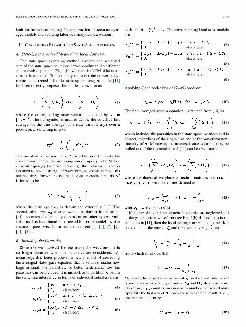
Due to the complexity of determining and analyti-cally, in this letter these functions are established numericallyusing a detailed simulation, which includes the necessaryparasitics. The state-space model and the system matrices
, and can be generated automatically usingwell-defined algorithms and software tools [13], [14]. There-after, the numerical procedure suggested here is similar to theparametric average-value modeling methodology that has beendemonstrated for synchronous machine-rectifier systems [15],[16]. The major point of this approach is to use the detailedsimulation for numerically calculating the key relationships(functions) needed for constructing the average-value model ofa certain well-defined form. In doing so, the effects of parasiticspresent in the detailed model become automatically included in
Fig. 2. Implementation of the proposed average-value model.
the numerically constructed functions, thus relieving the modeldeveloper from completing complicated analytical derivations.
To ensure that the final averaged model has full order, thefunctions and must be expressed in terms of the exter-nally controlled duty cycle and the fast state variable . De-pending on whether the large-signal or the small-signal model isrequired, establishing and may involvedifferent numerical procedures.
A. Large-Signal Transient Model
If the goal is to establish a large-signal average-value tran-sient model that is valid over a wide range of operating con-ditions, the functions and must be ob-tained for the operating region of interest. In the most generalcase, this region may be spanned by varying the duty cyclefrom a very small value (close to 0) to a very high value (close to1), and by varying the load resistance from very small (short-cir-cuit) to very high (open-circuit). This, in turn, requires multipleruns of a detailed simulation, which is easily implemented in aloop. In each run, the state variables are numerically averagedover the switching interval and subintervals to obtain , and
, respectively, from which the correction coefficientsare computed using (13). The variables resulting from each runalso include and . Once the loop with the detailed simula-tion has been ran, the resulting data are re-organized to obtainthe functions and . These functions arestored as the lookup tables with appropriate interpolation/ex-trapolations for future use. It is important to point out that since
and are algebraic functions of the con-trol input and fast state variable, they may be obtained fromsteady-state solutions as well as from transient studies producedby the detailed model.
For the class of dc–dc converters considered here, the formof the average-value model is defined by (12), which may berepresented by the diagram shown in Fig. 2. According to Fig. 2,for a given value of control variable and state vector , thefunctions and are evaluated and used to construct theaveraged state-space matrices. The final model is continuousand can be used for large-signal time-domain transient studies aswell as for direct numerical linearization and subsequent small-signal analysis, explained as follows.
IEEE TRANSACTIONS ON POWER ELECTRONICS, VOL. 21, NO. 4, JULY 2006 1145
B. Small-Signal Characterizations
If the averaged transient model of Fig. 2 has been alreadyconstructed, in contrast to the detailed model, it is continuousand can be numerically linearized about any operating pointof interest. Automatic linearization and subsequent state-spaceand/or frequency-domain analysis is supported by many numer-ical simulation tools, e.g., [17]. Thereafter, obtaining a localtransfer-function and/or frequency-domain characteristics for adesired operating point becomes a straightforward and almostinstantaneous procedure.
Based on (12) and (13), the small-signal characterization ofa particular operating point can also be obtained very rapidlywithout constructing the large-signal averaged model and/or ex-tensively running the detailed simulation. In particular, the keyelement of constructing a small-signal model is to capture theslope of functions and corresponding tothe desired operating point. In the small-signal sense, the nu-merically constructed functions and arecontinuous and may be assumed smooth around the given oper-ating point, whereas their local slope may be defined by a plane.Since the plane can be defined by as few as three points, the de-tailed simulation needs to be run at two more operating condi-tions that are slightly perturbed (e.g., 1 2%) and span the
and locally. These additional data pointsare then used in the model depicted in Fig. 2 instead of the pre-vious lookup tables, which yields a nonlinear continuous modelvalid locally for the small signal only. This model is then numer-ically linearized (similarly to the averaged large-signal model)and used to reconstruct the necessary transfer functions and/orsmall-signal characteristics.
IV. CASE STUDIES
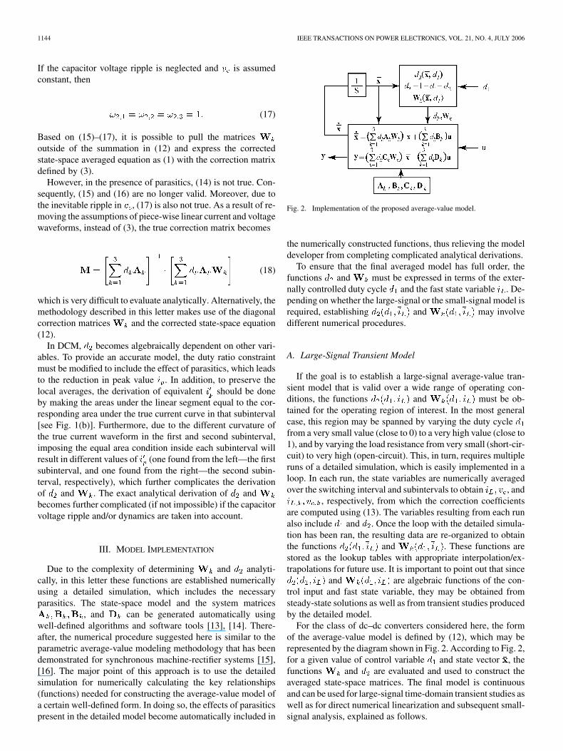
A hardware prototype of the converter depicted in Fig. 1with parameters given in the Appendix has been consideredfor the model validation. The corresponding detailed modelthat includes the basic parasitics shown in Fig. 1 has beenimplemented. The proposed average-value model has beenimplemented according to the methodology described inSection III. The converter efficiency has been calculated usingthe detailed model and is plotted in Fig. 3 for the consideredrange of operating conditions specified by the load resistanceand the control duty cycle. In the given converter, the parasitics(no exaggerations have been made) may result in 65%–85%efficiency in the practical region of operation, which is not un-common for small prototypes [7], [11]. Although the converterwould normally be operated in a high-efficiency region forpractical reasons, in general, it is more difficult to develop anaveraged model that would accurately capture performance in awide range of operating conditions, especially where the effectof losses is more pronounced.
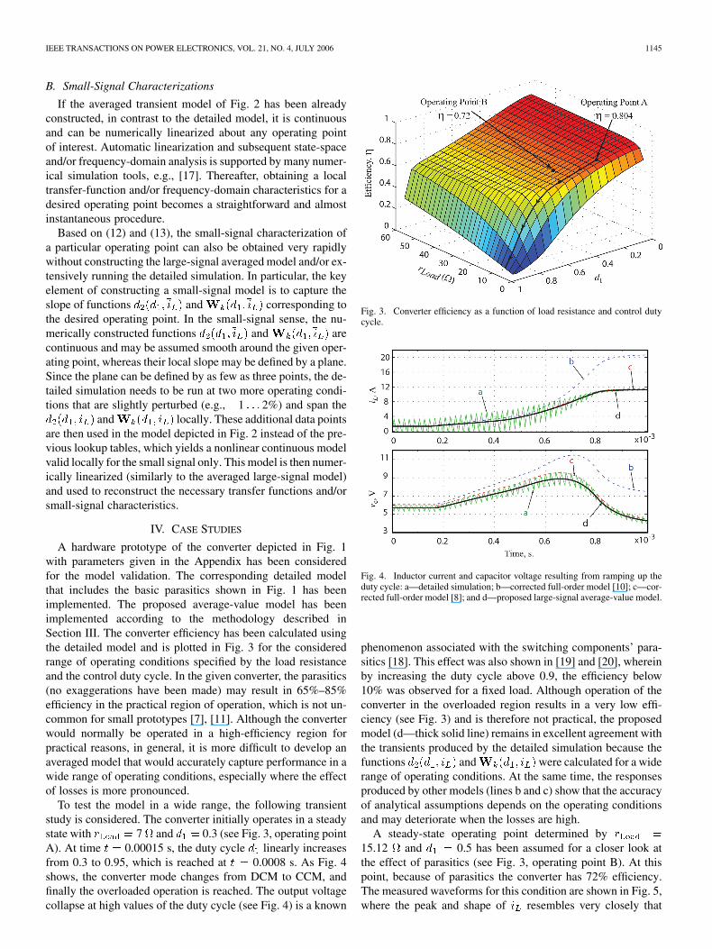
To test the model in a wide range, the following transientstudy is considered. The converter initially operates in a steadystate with 7 and 0.3 (see Fig. 3, operating pointA). At time 0.00015 s, the duty cycle linearly increasesfrom 0.3 to 0.95, which is reached at 0.0008 s. As Fig. 4shows, the converter mode changes from DCM to CCM, andfinally the overloaded operation is reached. The output voltagecollapse at high values of the duty cycle (see Fig. 4) is a known
Fig. 3. Converter efficiency as a function of load resistance and control dutycycle.
Fig. 4. Inductor current and capacitor voltage resulting from ramping up theduty cycle: a—detailed simulation; b—corrected full-order model [10]; c—cor-rected full-order model [8]; and d—proposed large-signal average-value model.
phenomenon associated with the switching components’ para-sitics [18]. This effect was also shown in [19] and [20], whereinby increasing the duty cycle above 0.9, the efficiency below10% was observed for a fixed load. Although operation of theconverter in the overloaded region results in a very low effi-ciency (see Fig. 3) and is therefore not practical, the proposedmodel (d—thick solid line) remains in excellent agreement withthe transients produced by the detailed simulation because thefunctions and were calculated for a widerange of operating conditions. At the same time, the responsesproduced by other models (lines b and c) show that the accuracyof analytical assumptions depends on the operating conditionsand may deteriorate when the losses are high.
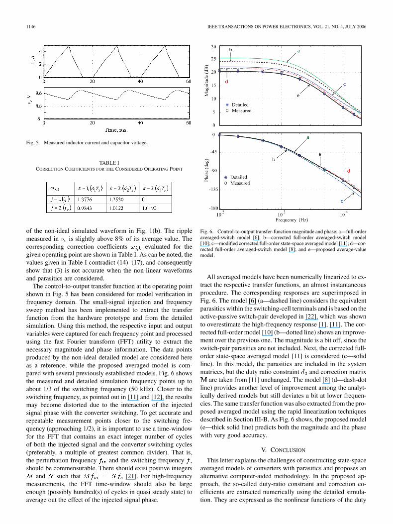
A steady-state operating point determined by15.12 and 0.5 has been assumed for a closer look atthe effect of parasitics (see Fig. 3, operating point B). At thispoint, because of parasitics the converter has 72% efficiency.The measured waveforms for this condition are shown in Fig. 5,where the peak and shape of resembles very closely that
1146 IEEE TRANSACTIONS ON POWER ELECTRONICS, VOL. 21, NO. 4, JULY 2006
Fig. 5. Measured inductor current and capacitor voltage.
TABLE ICORRECTION COEFFICIENTS FOR THE CONSIDERED OPERATING POINT
of the non-ideal simulated waveform in Fig. 1(b). The ripplemeasured in is slightly above 8% of its average value. Thecorresponding correction coefficients evaluated for thegiven operating point are shown in Table I. As can be noted, thevalues given in Table I contradict (14)–(17), and consequentlyshow that (3) is not accurate when the non-linear waveformsand parasitics are considered.
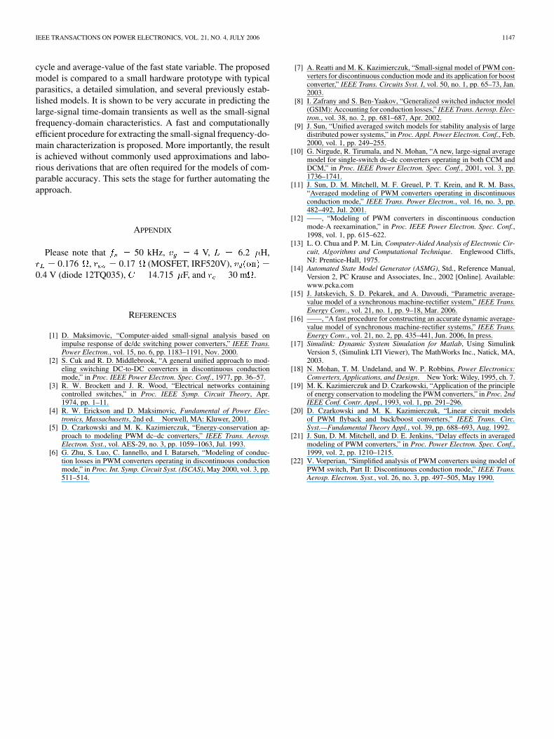
The control-to-output transfer function at the operating pointshown in Fig. 5 has been considered for model verification infrequency domain. The small-signal injection and frequencysweep method has been implemented to extract the transferfunction from the hardware prototype and from the detailedsimulation. Using this method, the respective input and outputvariables were captured for each frequency point and processedusing the fast Fourier transform (FFT) utility to extract thenecessary magnitude and phase information. The data pointsproduced by the non-ideal detailed model are considered hereas a reference, while the proposed averaged model is com-pared with several previously established models. Fig. 6 showsthe measured and detailed simulation frequency points up toabout 1/3 of the switching frequency (50 kHz). Closer to theswitching frequency, as pointed out in [11] and [12], the resultsmay become distorted due to the interaction of the injectedsignal phase with the converter switching. To get accurate andrepeatable measurement points closer to the switching fre-quency (approaching 1/2), it is important to use a time-windowfor the FFT that contains an exact integer number of cyclesof both the injected signal and the converter switching cycles(preferably, a multiple of greatest common divider). That is,the perturbation frequency and the switching frequencyshould be commensurable. There should exist positive integers
and such that [21]. For high-frequencymeasurements, the FFT time-window should also be largeenough (possibly hundred(s) of cycles in quasi steady state) toaverage out the effect of the injected signal phase.
Fig. 6. Control-to-output transfer-function magnitude and phase; a—full-orderaveraged-switch model [6]; b—corrected full-order averaged-switch model[10]; c—modified corrected full-order state-space averaged model [11]; d—cor-rected full-order averaged-switch model [8]; and e—proposed average-valuemodel.
All averaged models have been numerically linearized to ex-tract the respective transfer functions, an almost instantaneousprocedure. The corresponding responses are superimposed inFig. 6. The model [6] (a—dashed line) considers the equivalentparasitics within the switching-cell terminals and is based on theactive-passive switch-pair developed in [22], which was shownto overestimate the high-frequency response [1], [11]. The cor-rected full-order model [10] (b—dotted line) shows an improve-ment over the previous one. The magnitude is a bit off, since theswitch-pair parasitics are not included. Next, the corrected full-order state-space averaged model [11] is considered (c—solidline). In this model, the parasitics are included in the systemmatrices, but the duty ratio constraint and correction matrix
are taken from [11] unchanged. The model [8] (d—dash-dotline) provides another level of improvement among the analyt-ically derived models but still deviates a bit at lower frequen-cies. The same transfer function was also extracted from the pro-posed averaged model using the rapid linearization techniquesdescribed in Section III-B. As Fig. 6 shows, the proposed model(e—thick solid line) predicts both the magnitude and the phasewith very good accuracy.
V. CONCLUSION
This letter explains the challenges of constructing state-spaceaveraged models of converters with parasitics and proposes analternative computer-aided methodology. In the proposed ap-proach, the so-called duty-ratio constraint and correction co-efficients are extracted numerically using the detailed simula-tion. They are expressed as the nonlinear functions of the duty
IEEE TRANSACTIONS ON POWER ELECTRONICS, VOL. 21, NO. 4, JULY 2006 1147
cycle and average-value of the fast state variable. The proposedmodel is compared to a small hardware prototype with typicalparasitics, a detailed simulation, and several previously estab-lished models. It is shown to be very accurate in predicting thelarge-signal time-domain transients as well as the small-signalfrequency-domain characteristics. A fast and computationallyefficient procedure for extracting the small-signal frequency-do-main characterization is proposed. More importantly, the resultis achieved without commonly used approximations and labo-rious derivations that are often required for the models of com-parable accuracy. This sets the stage for further automating theapproach.
APPENDIX
Please note that 50 kHz, 4 V, 6.2 H,0.176 , 0.17 (MOSFET, IRF520V),
0.4 V (diode 12TQ035), 14.715 F, and 30 m .
REFERENCES
[1] D. Maksimovic, “Computer-aided small-signal analysis based onimpulse response of dc/dc switching power converters,” IEEE Trans.Power Electron., vol. 15, no. 6, pp. 1183–1191, Nov. 2000.
[2] S. Cuk and R. D. Middlebrook, “A general unified approach to mod-eling switching DC-to-DC converters in discontinuous conductionmode,” in Proc. IEEE Power Electron. Spec. Conf., 1977, pp. 36–57.
[3] R. W. Brockett and J. R. Wood, “Electrical networks containingcontrolled switches,” in Proc. IEEE Symp. Circuit Theory, Apr.1974, pp. 1–11.
[4] R. W. Erickson and D. Maksimovic, Fundamental of Power Elec-tronics, Massachusetts, 2nd ed. Norwell, MA: Kluwer, 2001.
[5] D. Czarkowski and M. K. Kazimierczuk, “Energy-conservation ap-proach to modeling PWM dc–dc converters,” IEEE Trans. Aerosp.Electron. Syst., vol. AES-29, no. 3, pp. 1059–1063, Jul. 1993.
[6] G. Zhu, S. Luo, C. Iannello, and I. Batarseh, “Modeling of conduc-tion losses in PWM converters operating in discontinuous conductionmode,” in Proc. Int. Symp. Circuit Syst. (ISCAS), May 2000, vol. 3, pp.511–514.
[7] A. Reatti and M. K. Kazimierczuk, “Small-signal model of PWM con-verters for discontinuous conduction mode and its application for boostconverter,” IEEE Trans. Circuits Syst. I, vol. 50, no. 1, pp. 65–73, Jan.2003.
[8] I. Zafrany and S. Ben-Yaakov, “Generalized switched inductor model(GSIM): Accounting for conduction losses,” IEEE Trans. Aerosp. Elec-tron., vol. 38, no. 2, pp. 681–687, Apr. 2002.
[9] J. Sun, “Unified averaged switch models for stability analysis of largedistributed power systems,” in Proc. Appl. Power Electron. Conf., Feb.2000, vol. 1, pp. 249–255.
[10] G. Nirgude, R. Tirumala, and N. Mohan, “A new, large-signal averagemodel for single-switch dc–dc converters operating in both CCM andDCM,” in Proc. IEEE Power Electron. Spec. Conf., 2001, vol. 3, pp.1736–1741.
[11] J. Sun, D. M. Mitchell, M. F. Greuel, P. T. Krein, and R. M. Bass,“Averaged modeling of PWM converters operating in discontinuousconduction mode,” IEEE Trans. Power Electron., vol. 16, no. 3, pp.482–492, Jul. 2001.
[12] ——, “Modeling of PWM converters in discontinuous conductionmode-A reexamination,” in Proc. IEEE Power Electron. Spec. Conf.,1998, vol. 1, pp. 615–622.
[13] L. O. Chua and P. M. Lin, Computer-Aided Analysis of Electronic Cir-cuit, Algorithms and Computational Technique. Englewood Cliffs,NJ: Prentice-Hall, 1975.
[14] Automated State Model Generator (ASMG), Std., Reference Manual,Version 2, PC Krause and Associates, Inc., 2002 [Online]. Available:www.pcka.com
[15] J. Jatskevich, S. D. Pekarek, and A. Davoudi, “Parametric average-value model of a synchronous machine-rectifier system,” IEEE Trans.Energy Conv., vol. 21, no. 1, pp. 9–18, Mar. 2006.
[16] ——, “A fast procedure for constructing an accurate dynamic average-value model of synchronous machine-rectifier systems,” IEEE Trans.Energy Conv., vol. 21, no. 2, pp. 435–441, Jun. 2006, In press.
[17] Simulink: Dynamic System Simulation for Matlab, Using SimulinkVersion 5, (Simulink LTI Viewer), The MathWorks Inc., Natick, MA,2003.
[18] N. Mohan, T. M. Undeland, and W. P. Robbins, Power Electronics:Converters, Applications, and Design. New York: Wiley, 1995, ch. 7.
[19] M. K. Kazimierczuk and D. Czarkowski, “Application of the principleof energy conservation to modeling the PWM converters,” in Proc. 2ndIEEE Conf. Contr. Appl., 1993, vol. 1, pp. 291–296.
[20] D. Czarkowski and M. K. Kazimierczuk, “Linear circuit modelsof PWM flyback and buck/boost converters,” IEEE Trans. Circ.Syst.—Fundamental Theory Appl., vol. 39, pp. 688–693, Aug. 1992.
[21] J. Sun, D. M. Mitchell, and D. E. Jenkins, “Delay effects in averagedmodeling of PWM converters,” in Proc. Power Electron. Spec. Conf.,1999, vol. 2, pp. 1210–1215.
[22] V. Vorperian, “Simplified analysis of PWM converters using model ofPWM switch, Part II: Discontinuous conduction mode,” IEEE Trans.Aerosp. Electron. Syst., vol. 26, no. 3, pp. 497–505, May 1990.