Embed Size (px)
Citation preview

NanoCMOS-Molecular Realization of Rijndael
Massoud Masoumi, Farshid Raissi, and Mahmoud Ahmadian ECE Dept., K. N. Toosi University of Technology, Tehran, Iran
[email protected], [email protected], and [email protected]
Abstract. This paper describes the implementation of the Advanced Encryption Standard Algorithm, Rijndael, in a new nanoscale technology, called CMOL. This technology consists of an array of conventional CMOS gates and a wiring network, which consists of a high density mesh of nanowires. The basic Modules of Rijndael were implemented using CMOL architecture. It is observed that the implementation in such a technology has considerable advantages compared to a conventional CMOS approach as regards to defect tolerance, speed, area and power consumption.
Keywords: Rijndael, VLSI realization, CMOL.
1 Introduction
In our days, the need for secure transparent protocols seems to be one of the most important issues in the communication standards and new reliable and flexible algorithms specially designed to face the demand for secure but simple and flexible cryptosystems. This demand has been accelerated by the emergence of large-scale, high speed communication networks. Therefore, VLSI design and realization of cryptosystems has been a motivational and challenging subject. The inherent advantages of using VLSI chips for encryption are speed and more physical security. Software encryption has other features like portability and flexibility but is slow and suffers from insecurity in several aspects of key management and program manipulation. In 1997, NIST decided that a new standard algorithm is needed because attacks like exhaustive key search exploiting the short key length of DES had been demonstrated. Through three Advanced Encryption Standard (AES) conferences, Rijndael [1] was selected as AES in October 2000. After adoption of Rijndael, its VLSI realization was taken into consideration and nowadays it is integrated in many various embedded applications like Web Servers, ATMs, Fiber Distributed Data Interfaces (FDDIs), smart cards, cellular phones… Since 2000, several architectures for efficient VLSI realization of AES algorithm have been proposed and their performance evaluated using ASIC libraries and FPGAs [2], [3], [4], [5], [6], [7]. Further integration or speed-up of such circuits will not be easily possible in conventional manners. The ongoing feature size reduction of silicon based CMOS technology which has been basis of the development of the semiconductor industry for the last three decades will run into severe physical and economic problems. The scaling of MOSFETs is entering the deep-nanosized regime in which fundamental limits of CMOS and technological challenges with regard the scaling of CMOS are

encountered [8], [9]. While traditional silicon based microelectronics is gradually approaching the end of its scaling [10], novel nanoelectronic solutions will be needed to surmount the physical and economic barriers of current semiconductor technology. A feasible scenario is the integration of silicon with nanoelectronic, i.e. a mixed CMOS/nano system [11]. This approach would allow a smooth transition and permit leveraging the beneficial aspects of both technologies. One potential alternative to supplement to or replace the CMOS microelectronics is the recently proposed semiconductor-nanowire-molecular architecture known as CMOL [12]. The basic idea for such circuits is to combine the advantages of current CMOS technology including flexibility and high fabrication yield with nanometer scale molecular devices, self assembled on a pre-fabricated nanowire fabric, enabling very high function density at modest fabrication cost. The implementation of such a structure via cross wire networks has been fully examined in literature [12], [13]. It seems at best at this point that CMOL circuits are suitable for embedded and stand-alone terabit memories and would be able to accomplish some tasks which are implemented by neural networks such as image processing, pattern recognition and classification [14], [15]. It is to this end that we are proposing that Rijndael can be implemented by CMOL technology and such implementation can bypass VLSI performance bottlenecks of this algorithm. Circuit density, speed and power consumption are three criteria which are of utmost importance in encryption VLSI realization and CMOL is by far the best scheme regarding these criteria. Moreover CMOL circuits have another advantage in comparison with regular CMOS circuits and are inherently defect tolerant [12], [13]. We have recently shown that basic modules of Rijndael can be implemented by CMOL technology with very interesting results [16]. The results we have obtained demonstrate that longer keys can be easily realized by CMOL, making unauthorized deciphering almost impossible. We had not obtained an estimate of power consumption of Rijndael’s basic modules on CMOL platform but the new results show that the power consumption of theses modules are reduced with a factor of 1000-2000 in comparison with CMOS implementation. In this paper we focus on nanotechnology as a new solution for removing VLSI cryptosystem realization bottlenecks. We describe how basic modules of Rijndael can be implemented in CMOL technology and present the new results obtained. The organization of the paper is as follows. Section 2 explains AES algorithm briefly. Section 3 introduces CMOL technology and CMOL FPGA as the most promising structure for CMOL circuits. In section 4 we describe how the basic building modules of Rijndael are realized in CMOL technology and give the results of implementation. Finally, in the conclusion we briefly summarize the results of our discussion.
2 Rijndael Algorithm
Rijndael has been developed and published by Daemen and Rijmen [1], [17]. This algorithm is a byte-oriented symmetric block cipher, composed of a sequence of four primitive functions, SubBytes, ShiftRows, MixColumns, and AddRoundKey, executed round by round. Rijndael supports any key length and block length between 128 bits and 256 bits that is a multiple of 32 bits independently. The number of
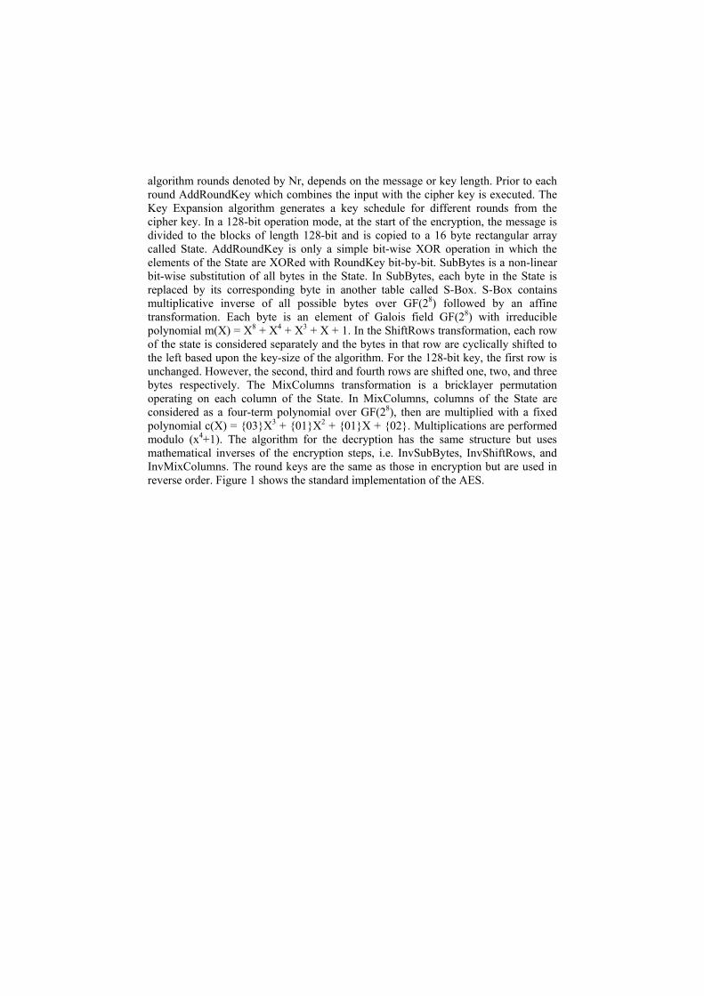
algorithm rounds denoted by Nr, depends on the message or key length. Prior to each round AddRoundKey which combines the input with the cipher key is executed. The Key Expansion algorithm generates a key schedule for different rounds from the cipher key. In a 128-bit operation mode, at the start of the encryption, the message is divided to the blocks of length 128-bit and is copied to a 16 byte rectangular array called State. AddRoundKey is only a simple bit-wise XOR operation in which the elements of the State are XORed with RoundKey bit-by-bit. SubBytes is a non-linear bit-wise substitution of all bytes in the State. In SubBytes, each byte in the State is replaced by its corresponding byte in another table called S-Box. S-Box contains multiplicative inverse of all possible bytes over GF(28) followed by an affine transformation. Each byte is an element of Galois field GF(28) with irreducible polynomial m(X) = X8 + X4 + X3 + X + 1. In the ShiftRows transformation, each row of the state is considered separately and the bytes in that row are cyclically shifted to the left based upon the key-size of the algorithm. For the 128-bit key, the first row is unchanged. However, the second, third and fourth rows are shifted one, two, and three bytes respectively. The MixColumns transformation is a bricklayer permutation operating on each column of the State. In MixColumns, columns of the State are considered as a four-term polynomial over GF(28), then are multiplied with a fixed polynomial c(X) = {03}X3 + {01}X2 + {01}X + {02}. Multiplications are performed modulo (x4+1). The algorithm for the decryption has the same structure but uses mathematical inverses of the encryption steps, i.e. InvSubBytes, InvShiftRows, and InvMixColumns. The round keys are the same as those in encryption but are used in reverse order. Figure 1 shows the standard implementation of the AES.
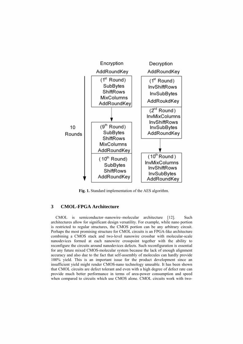
Fig. 1. Standard implementation of the AES algorithm.
3 CMOL-FPGA Architecture
CMOL is semiconductor–nanowire–molecular architecture [12]. Such architectures allow for significant design versatility. For example, while nano portion is restricted to regular structures, the CMOS portion can be any arbitrary circuit. Perhaps the most promising structure for CMOL circuits is an FPGA-like architecture combining a CMOS stack and two-level nanowire crossbar with molecular-scale nanodevices formed at each nanowire crosspoint together with the ability to reconfigure the circuits around nanodevices defects. Such reconfiguration is essential for any future mixed CMOS-molecular system because the lack of enough alignment accuracy and also due to the fact that self-assembly of molecules can hardly provide 100% yield. This is an important issue for the product development since an insufficient yield might render CMOS-nano technology unusable. It has been shown that CMOL circuits are defect tolerant and even with a high degree of defect rate can provide much better performance in terms of area-power consumption and speed when compared to circuits which use CMOS alone. CMOL circuits work with two-
terminal nanodevices whose are electrically activated or deactivated at the cross-points of the mesh and their fabrication is substantially less challenging than their three-terminal counterparts. Of course the limited functionality of two terminal devices is compensated by transistors of the CMOS subsystem. Two-terminal nanodevices provide us with high degree of integrability while CMOS devices provide us with other necessary functions such as voltage gain, address decoding and output signal sensing enabling digital performance with much speed and low power consumption. Novel ideas on the type of molecules and their connection scheme have been proposed and current estimate suggest that within 10-15 years such crossbar implementation of two-terminal devices becomes quite possible [12], [13]. A simplified diagram of a mixed CMOS/nano system and the hybrid complementary metal oxide semiconductor/molecular circuit structure are shown in figures 2 and 3 respectively.
Fig. 2. A simplified diagram of a mixed CMOS/nano system.

Fig. 3. The hybrid complementary metal oxide semiconductor/molecular circuit contains a molecule that may function as a latching switch activated by two input signals
The general configuration of a CMOL FPGA and a CMOL cell, as proposed in [13] is provided in Figures 4(a) and 4(b) respectively. Cross type nanowires (crossnet) are placed over a regularly placed matrix of CMOS cells. Nanomolecular two terminal devices are to be self assembled between the wires at each cross point. These molecules either work as latching switches or similar to diodes with a rectifying characteristic. The interesting proposed alignment of nanowires with respect to underlying CMOS cells, which is rotated by a certain angle, makes it possible to address each and every molecule. This is accomplished by CMOS cells which are accessible through column and row lines. The configuration of unit cell which is made of a CMOS NOT gate is shown in Figure 4(c) with its associated row and column lines. So called connection pins are placed on each cell to create connections to the bottom and top wire meshes. For example, the inputs are connected to the bottom nanowire and output to the top nanowire. In this manner several molecules are connected to each cell. To provide for a universal FPGA architecture, there are small breaks in nanowires in a periodic fashion. A square shaped connectivity domain can be defined for each cell. Connectivity domain is a region around the initial cell containing 2r(r-1)-1 other cells, in which input or output of the original cell can be connected to any cell in this region. r is a positive integer number called connectivity radius. In the Figure 4(a) the connectivity radius is 3.

This corresponds to the square shaped area in Figure 4(a). If all the molecules were conducting current, all the inputs and outputs of all the cells would be connected and circuits won’t work. Molecules, however, are considered to act as latching switches. We can choose to make the appropriate ones to conduct their corresponding address lines. For example, the molecule connecting the output of each cell to its input must always be off or open. The same is true for all other molecules that connect the output to its connectivity domain. Now, each cell with its associated molecular devices can be considered as a NOR gate as given in Figure 4(d). Having NOT and NOR is sufficient to implement any Boolean function.
Fig. 4. The topology of a CMOL FPGA., (a) Each rectangular cell is a NOT gate whose input and output are shown by black dots. Input and outputs makes contact to separate layers of nanowires. (b) The CMOS transistor which makes each inverter cell with its associated address lines and so called “pass” transistors. (c) The molecules which have been turned ON and are shown by dark gray at the crosspoint of the wire meshes. Other connections whose molecules are not turned ON are not shown, (d) Circuit representation of the three input NOR gate which is equivalent to a diode-resistor connected NOR gate.
Due to the uniformity of the nanowiring/nanodevices levels of CMOL, they do not need to be precisely aligned with each other and the underlying CMOS stack. In addition, CMOL circuits are inherently defect-tolerant, since there are M = 2r(r-1) -1

nanodevices in each cell. In some cases, even a 75% loss of molecular devices due to misalignment results in acceptable functionality. After initial mapping on CMOL fabric and configuration stage, each cell whose associated molecules are not properly functioning may be swapped with another adjacent cell in its connectivity domain and the circuit would operate properly. Such gate swapping is not provided by physical relocation of gates but by using a new routing. This is shown in Figure 5 and the reader is encouraged to refer to references [13] for detail. It has been reported that, from the software point of view, a CMOL tile can be treated in the same way as that of the island-type CMOS FPGA. Indeed, we first map the original pre-optimized logic circuit onto a network of NOR gates (with a certain maximum fan-in) and latches (if any), to produce a netlist. Next, we fix a certain number (N) of CMOS cells inside each tile to perform logic operations, while the rest T−N CMOS cells are committed to routing [18].
Fig. 5. Example of a circuit reconfiguration, (a) NOR-NOT equivalent circuit of an XOR gate, (b) mapping the circuit on a 6*8 CMOL rectangular block. At least one of the molecules of gate C is faulty and therefore this gate to be relocated. (c) The intersect of repair regions of input and output cells of gate C, i.e. gates A and E houses gate D, hence the repair region of this gate is calculated again. Since gate C lies in the repair region of gate D these gates can be swapped, connection quality permitting. Here r = 3 and there are 11 other cells in the connectivity region of each cell
4 Implementation of Rijndael’s Basic Transformations Using CMOL Scheme
In this section we discuss issues related to the implementation of Rijndael’s basic building blocks, i.e. MixColumns and SubBytes. Several architectural and algorithmic optimization techniques have been proposed for efficient implementation of the AES algorithm. The aim of these optimization techniques is to reduce the critical path, chip area and power consumption of AES chips and are developed to suit the different demand of applications. We demonstrate that if these proposed architectures are

implemented in CMOL performance of AES chips would be much improved. No optimization can be performed on the hardware structure of ShiftRows and AddRoundKey, since no logic gates are needed for the former transformation and only one step of XOR is needed for the latter. We present the new results obtained from realization and performance estimation of MixColumns and SubBytes on a typical CMOL fabric and compare them with their purely CMOS counterparts. While much of the analysis in this paper is applicable to several other cryptographic algorithms, we focus on Rijndael as a very good typical example.
4.1 Implementation of MixColumns
Over the years many implementations, with different levels of optimizations have been presented and there are several architectures for efficient implementation for MixColumns. A good possible implementation in the terms of speed and resource sharing as proposed in [7] is shown in the figure 6. In this figure, ‘XTime’ block implements the constant multiplication by {02} in GF(28). ‘XTime’ block consists of 3 XOR gates and its critical path includes only one XOR gate [6].
Fig. 6. Efficient implementation of MixColumns transformation
We represented this transformation to the fan-in two NOR gates and inverters, the only available logic primitives on a standard CMOL FPGA, as shown in Figure 8. In order to compare the performance of the implementation on CMOL with its CMOS counterpart and to evaluate the effectiveness of our approach, first we simulated it using VHDL codes with structural logic description and synthesized it on Spartan 3, the fastest commercially available FPGA from Xilinx family which is fabricated with 90-nm CMOS technology. The basic unit of such an FPGA is a slice consisting of two
4-input LUTs. Xilinx ISE 6.2i was used to synthesize the design and provide post-placement timing results. The results of synthesis showed that it consumes 60 logic cells and the total logic delay is about 0.62 ns. With the cell (tile) area approximated as 2100 um2 [13], it means that the circuit will occupy about 126000 um2 on the chip. Then, we mapped it manually on a 32*40 CMOL FPGA fabric with connectivity radius r = 12 and CMOL parameters as FCOMS = 32 nm, Fnano = 8 nm. The way to estimate density, speed, and power consumption of CMOL circuits has been described in [13]. If we estimate the cell area Acell as 64(FCMOS)2 [12], [13] with logic depth equal to 28, the same implementation on CMOL FPGA with will result the total gate delay equal to 0.15 ns, the total area equal to 84 µm2 and the area-delay product equal to 12.6 µm2 ns. A computer program was written for finding a pseudo-optimum yield-optimized gate placement. Then we performed Mont Carlo simulation for reconfiguration algorithm. The circuit yield was about %98.5 for defect rate of molecular devices up to 25%. However, reconfigurable circuits are not yet frequently embedded into portable applications and our interest for power consumption was driven by another reason. Indeed, for the implementation of cryptographic algorithms, not only the speed and the size of the circuit are important, but also their security against implementation attacks. For example, in Differential Power Analysis, it is assumed that the power consumption of a device is correlated with the data handled. The power dissipation of the two implementation approaches could be estimated and compared. Ignoring the leakage current of molecular devices, the average total power consumption of a CMOL gate may be estimated as a sum of two constituents, the static power PON due to currents ION, and dynamic power Pdyn due to the recharging of nanowire capacitances. Considering the subject that the total power consumed per unit circuit area for CMOL FPGAs are limited at the level P/A = 200 W cm-2 [12], [13] we can estimate the total power dissipated at each CMOL cell by using a rule of thumb. With FCMOS = 32 nm, ACell will be equal to 6.5536*10-11 cm2 which means that there are about 1.52*1010 CMOL cell cm-2, each cell dissipating about 0.13 nW. Hence, the MixColumns module will dissipate about 0.16 mW. The power consumption of this transformation on Spartan-3 was estimated using ISE power analyzer and it was about 335 mW, about 2000 times larger than CMOL implementation. This estimate is close to the one given by Likharev. Recently he has implemented a 32-bit Kogge-stone adder on a CMOL FPGA fabric and has reported that power consumption of the circuit is 0.33 mW [12]. It is easy to justify this great difference between the power consumption of the CMOL and CMOS approaches. Most current CMOS FPGAs are SRAM-programmable, meaning that SRAM bits are connected to the configuration points in the FPGA, and programming these SRAM cells configures the device. These components are based on the static CMOS memory technology. Please notice that a 3-input NOR gate is implemented in CMOL technology by using only an inverter and four molecules, i.e. only one NMOS and one PMOS transistor, while it needs 3 PMOSs and 3 NMOSs to be implemented in a typical static CMOS technology. While major part of the power consumed in a CMOS FPGA is dissipated in its routing, interconnects, logic and clocking resources [19], CMOL FPGA has a completely different structure in which information is stored in molecules which consume very smaller energy in comparison with CMOS transistors. Also, the nanowiring section of CMOL FPGA has a very smaller effective capacitance in comparison of wiring and routing section of CMOS FPGAs [12], [13],
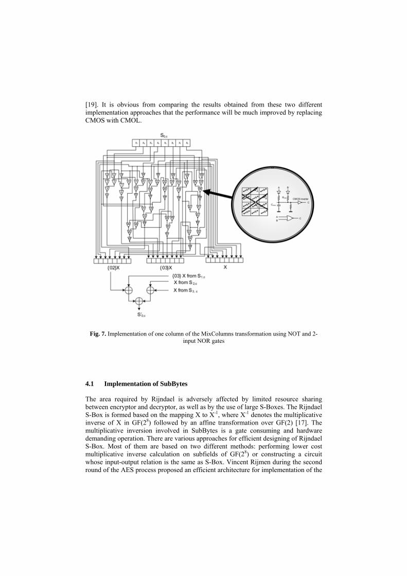
[19]. It is obvious from comparing the results obtained from these two different implementation approaches that the performance will be much improved by replacing CMOS with CMOL.
Fig. 7. Implementation of one column of the MixColumns transformation using NOT and 2-input NOR gates
4.1 Implementation of SubBytes
The area required by Rijndael is adversely affected by limited resource sharing between encryptor and decryptor, as well as by the use of large S-Boxes. The Rijndael S-Box is formed based on the mapping X to X-1, where X-1 denotes the multiplicative inverse of X in GF(28) followed by an affine transformation over GF(2) [17]. The multiplicative inversion involved in SubBytes is a gate consuming and hardware demanding operation. There are various approaches for efficient designing of Rijndael S-Box. Most of them are based on two different methods: performing lower cost multiplicative inverse calculation on subfields of GF(28) or constructing a circuit whose input-output relation is the same as S-Box. Vincent Rijmen during the second round of the AES process proposed an efficient architecture for implementation of the
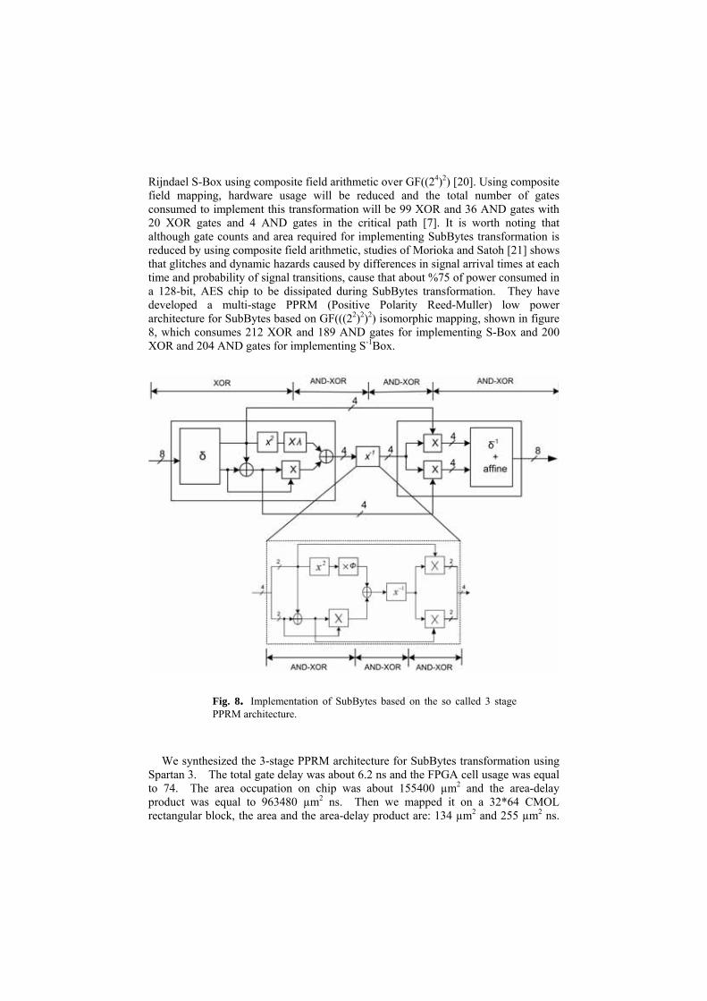
Rijndael S-Box using composite field arithmetic over GF((24)2) [20]. Using composite field mapping, hardware usage will be reduced and the total number of gates consumed to implement this transformation will be 99 XOR and 36 AND gates with 20 XOR gates and 4 AND gates in the critical path [7]. It is worth noting that although gate counts and area required for implementing SubBytes transformation is reduced by using composite field arithmetic, studies of Morioka and Satoh [21] shows that glitches and dynamic hazards caused by differences in signal arrival times at each time and probability of signal transitions, cause that about %75 of power consumed in a 128-bit, AES chip to be dissipated during SubBytes transformation. They have developed a multi-stage PPRM (Positive Polarity Reed-Muller) low power architecture for SubBytes based on GF(((22)2)2) isomorphic mapping, shown in figure 8, which consumes 212 XOR and 189 AND gates for implementing S-Box and 200 XOR and 204 AND gates for implementing S-1Box.
Fig. 8. Implementation of SubBytes based on the so called 3 stage PPRM architecture.
We synthesized the 3-stage PPRM architecture for SubBytes transformation using Spartan 3. The total gate delay was about 6.2 ns and the FPGA cell usage was equal to 74. The area occupation on chip was about 155400 µm2 and the area-delay product was equal to 963480 µm2 ns. Then we mapped it on a 32*64 CMOL rectangular block, the area and the area-delay product are: 134 µm2 and 255 µm2 ns.

While it dissipates approximately about 389 mW on Spartan 3 (estimation was obtained using Xilinx ISE 6.2i power analyzer) it consumes about 0.26 mW on a 32*64 CMOL fabric, about 1500 times less than its CMOS counterpart. Again we found a pseudo-optimum yield-optimized gate placement and performed Mont Carlo simulation for reconfiguration algorithm. The circuit yield was about %98.5 for defect rate of molecular devices up to 20%. It is observed that the basic block transformations of Rijndael can be implemented by CMOL with much improvement in speed, power consumption, and chip area.
5 Conclusions
In this paper we presented a new methodology based on mixed CMOS/nano circuits for future VLSI realization of Rijndael algorithm and showed the suitability of the implementation of Rijndael in CMOL. High speed, very small required area, very low power consumption and defect tolerance of CMOL circuits along with the possibility of designing long key encryption make CMOL as an optimum possible platform for encryption VLSI realization in the future. Nanoelectronic and mixed CMOS/nano systems are steel quite young and will require new design and fabrication paradigm but can lead to higher levels of computation and many other beneficial aspects.
References
1. Daemen, J, and Rijmen, V.: AES Proposal Rijndael, National Institute of Standards and Technology, July 2001
2. Fischer, V, and Drutarovsky, M.: Two Methods of Rijndael Implementation in Reconfigurable Hardware Proc. CHES, Paris, France (2001) 77-92
3. Sklavos, N, and Koufopavlou, O.: Architectures and VLSI Implementation of the AES-Proposal Rijndael IEEE Trans Computers, 51, 12 (2002) 1454-59
4. Lu, C, C, and Tseng Y, S.: Integrated Design of AES (Advanced Encryption Standard) Encryptor and Decryptor, in Proc. IEEE Int. Conf. Application Specific Systems, Architectures Processors (2002) 277-285
5. Satoh, A, Morioka, S, Takano, K, and Munetoh, S.: A Compact Rijndael Hardware Architecture S-BOX Optimization, in Proc. ASIACRYPT 2001, Gold Coast, Australia (2000) 239-254
6. Zhang, X, and Parhi, K, K.: Implementation Approaches for the Advanced Encryption Standard Algorithm, IEEE Circuits Mag., 2, 4 (2002) 24-46
7. Zhang, X, and Parhi, K, K.: High-Speed VLSI Architectures for the AES Algorithm, IEEE Trans. Very Large Scale Integration (VLSI) Systems, 12, 9 (2004) 957-967
8. Fortes, J.: Future challenges in VLSI System Design, Proceedings IEEE Computer Society Annual Symposium on VLSI (ISVLSI’03) (2003) 5-7
9. Likharev K, K, and Strukov, D, B.: Electronics Below 10 nm, Nano and Giga Challenges in Microelectronics, (Amsterdam: Elsevier) (2003) 27-68
10. International Technology Roadmap for Semiconductors (ITRS), 2004, Update, available online at http://public. itrs. net/
11. Ziegler, M, M, and Stan, M, R.: CMOS/nano Co-Design for Crossbar-Based Molecular Electronic Systems, IEEE Trans. Nanotechnology, 2 (4) (2003) 217–230
12. Likharev K, K, and Strukov, D, B.: CMOL: Devices, Circuits, and Architectures, available online at http://www-mcg.uni-regensburg.de/pages/admol/book/chapter_16.html/book/chapter_16.html
13. Strukov, D, B, and Likharev, K, K.: CMOL FPGA: a Reconfigurable Architecture for Hybrid Digital Circuits with Two-Terminal Nanodevices, Nanotechnology, 16 (2005) 888-900
14. Likharev, K, K, Türel, Ö, Lee, J, H, and Ma, X.: Architectures for Nanoelectronic Implementation of Artificial Neural Networks: New Results, Neurocomputing, 64, 1 (2005) 271-283
15. Strukov, D, and Likharev, K, Prospects for Terabit-Scale Nanoelectronic Memories, Nanotechnology, 16 (2005) 137-38
16. Masoumi, M, Raissi, F, Ahmadian, M, and Keshavarzi, P.: Design and Evaluation of Basic Standard Encryption Algorithm Modules using Nanosized CMOS-Molecular Circuits, Nanotechnology, 17 (2006) 89-99
17. Daemen, J, and Rijmen, V.: The Design of Rijndael, Springer (2002) 18. Strukov, D, B, and Likharev, K, K.: A Reconfigurable Architecture for Hybrid
CMOS/Nanodevice Circuits, available online at: http://portal.acm.org/affiliated/citation.cfm?id=1117221&coll=ACM&dl=guide
19. Standaert, F, X.: Secure and Efficient Use of Reconfigurable Hardware Devices in Symmetric Cryptography, Ph. D. Thesis, University of Catholique de Louvain, Belgium, 2004.
20. Rijmen, V, Efficient Implementation of Rijndael S-Box, available online at: www.iaik.tugraz.at/research/ krypto/AES/old/~rijmen/rijndael/sbox.pdf
21. Morioka, S, and Satoh, A, An Optimized S-Box Circuit Architecture for Low Power AES Design, in Proc. of Cryptographic Hardware and Embedded Systems (CHES) 2002, San Francisco, USA (2002) 172-186