Embed Size (px)
Citation preview
Lattice Matching of
Epitaxial Rare-Earth-doped
Dielectric PLD-Films
Dissertation
zur Erlangung des Doktorgradesdes Department Physikder Universitat Hamburg
vorgelegt von
Bilge Ileri
aus Hamburg
Hamburg2007
Gutachter der Dissertation: Prof. Dr. G. Huber
Prof. Dr. W. Hansen
Gutachter der Disputation: Prof. Dr. G. Huber
Priv. Doz. Dr. V. Baev
Datum der Disputation: 14.02.2008
Vorsitzender des Prufungsausschusses: Dr. K. Petermann
Dekan der Fakultat fur Mathematik,Informatik und Naturwissenschaften: Prof. Dr. A. Fruhwald
Vorsitzender des Promotionsausschusses Prof. Dr. G. Huber

SOLI DEO GLORIA
(Phil 2:13)

Abstract
Abstract
Bilge Ileri, Lattice Matching of Epitaxial Rare-Earth-doped Dielectric PLD-Films
The increasing demand of integrated optical devices requires the fabrication of high-quality optically active thin films. This work focuses on lattice matched dielectric ox-ide thin films. The investigated film materials include sesquioxides, orthovanadates andaluminum garnets, which are promising materials as they are well-known hosts for rare-earth-doped solid-state lasers with superior mechanical and thermal properties (e. g. lowphonon energies, large thermal conductivity).
Highly crystalline rare-earth-doped films of optical quality were grown by the pulsedlaser deposition (PLD) technique on single-crystal substrates of α-Al2O3, LiYF4, Y2O3,ScLuO3, YVO4, and Y3Al5O12. Different possibilities of lattice matching were investi-gated by heteroepitaxy of Al2O3–ScLuO3, ScLuO3–Al2O3 and LiYF4–Lu2O3 substrate–film systems and by homo- and quasi-homoepitaxy of Y2O3–RE2O3, YVO4–REVO4 andY3Al5O12–RE3Al5O12 substrate–film systems. The lattice matching in the quasi-homo-epitaxial systems was realized by admixing the (Gd, Lu)-amount to match the yttrium-based substrate material. Lattice matching of up to 99.88% (heteroepitaxy) and 99.79%(quasi-homoepitaxy) was realized.
The film growth was studied by in-situ reflection high-energy electron diffraction (RHEED).Continuous layer-by-layer growth was observed for all three quasi-homoepitaxial substrate–film systems. The crystal structure of the films was determined by ex-situ X-ray diffrac-tion (XRD) analysis. These measurements reveal that the films are highly textured alongthe default substrate direction. However, subplantation effects of high-energy plasmaspecies and subsequent particle interdiffusion into the substrate matrix are indicated inheteroepitaxy at too high deposition temperatures.
Besides in-situ RHEED monitoring and ex-situ XRD analysis, the surface morphology ofthe thin films was studied by atomic force microscopy (AFM). For better comparison andin order to achieve an arranged atomically flat surface with terraces of monolayer stepheight (2 – 5 A), the substrates were annealed prior to deposition. The annealing duration,atmosphere and temperature differed according to the substrate material. In general, theresulting film surface was very smooth. In some cases three-dimensional island formationcould be verified in good agreement with the corresponding RHEED measurements. Amulti-level surface morphology with monolayer step heights of 5 A each (half the filmlattice constant) was observed for a 1 � m two-dimensional layer-by-layer grown latticematched Nd:(Gd, Lu)2O3 film on (100) Y2O3 substrate.
Optical properties of the rare-earth-doped films were studied by spectroscopic measure-ments in the (vacuum-) ultraviolet and visible spectral-range. The emission and excitationspectra of the Eu3+-doped films look similar to those of the corresponding single-crystallinebulk materials, i. e. the symmetry around the Eu3+ ions is preserved. Depending on thefilm matrix and its number of different lattice sites and symmetries available for the rare-earth ions, the existence of additional ions in mixed (Gd, Lu)-films can in some casesdisturb the band structure (CTS and ES) of the film lattice.
i
Kurzfassung
Bilge Ileri, Gitteranpassung von epitaktischen SE-dotierten dielektrischen PLD-Schichten
Das Interesse an neuen Bauteilen fur die integrierte Optik erfordert zunehmend die Her-stellung dunner, optisch aktiver Schichten. Da dielektrische Oxide wie Sesquioxide, Ortho-vanadate und Aluminium-Granate aufgrund ihrer mechanischen und thermischen Eigen-schaften fur ein solches Aufgabengebiet sehr gut geeignet und bereits als Wirtsgitter furdie Seltenen Erden (SE) in Festkorperlasern im Einsatz sind, wird in dieser Arbeit dieGitteranpassung dunner dielektrischer Oxidschichten untersucht.
Mit dem Pulsed Laser Deposition (PLD)-Verfahren konnten kristalline Selten-Erd-dotierteSesquioxid-, Orthovanadat-, und Aluminium Granatschichten von optischer Qualitat aufα-Al2O3-, LiYF4-, Y2O3-, ScLuO3-, YVO4- und Y3Al5O12-Substraten hergestellt werden.Die verschiedenen Moglichkeiten der Gitteranpassung wurden bei Substrat–Schicht Sys-temen in der Heteroepitaxie von Al2O3–ScLuO3, ScLuO3–Al2O3 und LiYF4–Lu2O3 sowieder Homo- und Quasihomoepitaxie von Y2O3–RE2O3, YVO4–REVO4 und Y3Al5O12–RE3Al5O12 untersucht. Durch Abmischung des (Gd, Lu)-Anteils wurde in quasihomoepi-taktischen Systemen eine Gitteranpassung zu dem Yttrium-basierten Substratmaterialerzielt. Gitteranpassungen von bis zu 99.88% (Heteroepitaxie) und 99.79% (Quasiho-moepitaxie) konnten somit realisiert werden.
Durch Einsatz von in-situ Reflection High-Energy Electron Diffraction (RHEED) konntedas Schichtwachstum untersucht werden. Kontinuierliches Frank-van-der-Merve-Wachs-tum (layer-by-layer) konnte bei allen drei quasihomoepitaktischen Systemen beobachtetwerden. Mit Rontgenbeugung (XRD) wurde die Kristallstruktur der Schichten bestimmtund ein hochtexturiertes Wachstum in die jeweilige, vom Substrat vorgegebene Richtungfestgestellt. In der Heteroepitaxie konnte in Zusammenhang mit zu hohen Substrattem-peraturen Subplantation von hochenergetischen Teilchen aus dem Plasma mit anschließen-der Interdiffusion in die Substratmatrix zugeordnet werden.
Die Oberflachenbeschaffenheit der Schichten wurde mit Rasterkraftmikroskopie (AFM)untersucht. Zum besseren Vergleich der Schichtoberflache erfolgte eine thermische Vor-behandlung der Substrate, mit der geordnete, atomar glatte Oberflachen erzielt wur-den. Anhand einer Stufenbildung konnte die Aufteilung der jeweiligen Einheitszelle inverschiedene Lagen (2 – 5 A) beobachtet werden. Die Schichtoberflachen waren in derRegel atomar glatt, wobei in Ubereinstimmung mit RHEED in einigen Fallen auch 3D-Inselbildung beobachtet wurde. Fur eine gitterangepasste, 1 � m dicke Nd:(Gd, Lu)2O3-Schicht ergab sich eine Oberflache mit Stufenbildung von jeweils 5 A, welches der Halfteeiner Einheitszelle entspricht.
Die optischen Eigenschaften der Selten-Erd-dotierten Schichten wurden durch spektro-skopische Messungen im (Vakuum-)Ultravioletten und sichtbaren Spektralbereich be-stimmt. Dabei entsprechen die Emissions- und Anregungsspektren denen eines Volu-menkristalls, d. h. die lokale Symmetrie der Eu3+-Ionen ist erhalten. In Abhangigkeitvon der Kristallmatrix und der Anzahl an verschiedenen Symmetrieplatzen im Gitterfuhrte das Hinzufugen eines zusatzlichen Ions in (Gd, Lu)-Schichten zu einer Storung derBandstruktur (CTS und ES) in der kristallinen Schicht.
ii
Contents
Abstract . . . . . . . . . . . . . . . . . . . . . . . . . . . . . . . . . . . . . . . . iKurzfassung . . . . . . . . . . . . . . . . . . . . . . . . . . . . . . . . . . . . . . ii
List of Symbols and Abbreviations vii
1 Introduction 1
1.1 Motivation . . . . . . . . . . . . . . . . . . . . . . . . . . . . . . . . . . . . 11.2 Structure of this Thesis . . . . . . . . . . . . . . . . . . . . . . . . . . . . . 3
2 Materials 5
2.1 Sesquioxides . . . . . . . . . . . . . . . . . . . . . . . . . . . . . . . . . . . 52.2 Corundum . . . . . . . . . . . . . . . . . . . . . . . . . . . . . . . . . . . . 102.3 Yttrium Aluminum Garnet . . . . . . . . . . . . . . . . . . . . . . . . . . . 112.4 Orthovanadates of Yttrium and Gadolinium . . . . . . . . . . . . . . . . . 122.5 Lithium Yttrium Fluoride . . . . . . . . . . . . . . . . . . . . . . . . . . . 13
3 Lanthanide Dopants 17
3.1 The Free Ion . . . . . . . . . . . . . . . . . . . . . . . . . . . . . . . . . . . 183.2 The Lanthanide Ion in a Crystal Matrix . . . . . . . . . . . . . . . . . . . 21
3.2.1 Intraconfigurational 4f-4f Transitions . . . . . . . . . . . . . . . . . 223.2.2 Interconfigurational 4f-5d Transitions . . . . . . . . . . . . . . . . . 233.2.3 Charge Transfer Transitions . . . . . . . . . . . . . . . . . . . . . . 243.2.4 Vibrations of the Host Lattice . . . . . . . . . . . . . . . . . . . . . 25
3.3 Europium as Probe Ion . . . . . . . . . . . . . . . . . . . . . . . . . . . . . 28
4 Pulsed Laser Deposition 31
4.1 Laser-Target Interactions . . . . . . . . . . . . . . . . . . . . . . . . . . . . 334.2 The Plasma Plume . . . . . . . . . . . . . . . . . . . . . . . . . . . . . . . 39
5 Lattice Matched Thin Films 45
5.1 Growth Mechanisms . . . . . . . . . . . . . . . . . . . . . . . . . . . . . . 465.2 Combination of Different Lattices . . . . . . . . . . . . . . . . . . . . . . . 505.3 Investigated Systems . . . . . . . . . . . . . . . . . . . . . . . . . . . . . . 53
6 Thin Film Preparation 57
6.1 Pre-Deposition Substrate Treatment . . . . . . . . . . . . . . . . . . . . . 656.2 Reflection High-Energy Electron Diffraction . . . . . . . . . . . . . . . . . 67
iii
Contents
7 Analytical Techniques 75
7.1 X-Ray Diffraction . . . . . . . . . . . . . . . . . . . . . . . . . . . . . . . . 757.2 Ellipsometry and Reflectometry . . . . . . . . . . . . . . . . . . . . . . . . 807.3 Atomic Force Microscopy . . . . . . . . . . . . . . . . . . . . . . . . . . . . 837.4 Optical Spectroscopy . . . . . . . . . . . . . . . . . . . . . . . . . . . . . . 84
7.4.1 Fluorescence and Excitation Measurements . . . . . . . . . . . . . . 857.4.2 Lifetime Measurements . . . . . . . . . . . . . . . . . . . . . . . . . 867.4.3 VUV Measurements . . . . . . . . . . . . . . . . . . . . . . . . . . 87
8 Characterization of Heteroepitaxial Thin Films 89
8.1 Composite Sesquioxide Films on Sapphire . . . . . . . . . . . . . . . . . . 898.1.1 Lattice Matching . . . . . . . . . . . . . . . . . . . . . . . . . . . . 898.1.2 Structural Characterization . . . . . . . . . . . . . . . . . . . . . . 908.1.3 Surface Structure and Topography . . . . . . . . . . . . . . . . . . 958.1.4 Spectroscopic Analysis . . . . . . . . . . . . . . . . . . . . . . . . . 97
8.2 Sapphire Films on Composite Sesquioxide . . . . . . . . . . . . . . . . . . 1038.2.1 Lattice Matching and Structural Characterization . . . . . . . . . . 1038.2.2 Surface Structure and Topography . . . . . . . . . . . . . . . . . . 1058.2.3 Spectroscopic Analysis . . . . . . . . . . . . . . . . . . . . . . . . . 106
8.3 Lutetia Films on Lithium Yttrium Fluoride . . . . . . . . . . . . . . . . . 1078.3.1 Lattice Matching and Structural Characterization . . . . . . . . . . 1078.3.2 Surface Structure and Topography . . . . . . . . . . . . . . . . . . 1098.3.3 Spectroscopic Analysis . . . . . . . . . . . . . . . . . . . . . . . . . 110
8.4 Summary and Discussion . . . . . . . . . . . . . . . . . . . . . . . . . . . . 112
9 Characterization of Homo- and Quasi-Homoepitaxial Thin Films 115
9.1 Sesquioxide Films on Yttria . . . . . . . . . . . . . . . . . . . . . . . . . . 1159.1.1 Lattice Matching . . . . . . . . . . . . . . . . . . . . . . . . . . . . 1159.1.2 Structural Characterization . . . . . . . . . . . . . . . . . . . . . . 1169.1.3 Surface Structure and Topography . . . . . . . . . . . . . . . . . . 1249.1.4 Spectroscopic Analysis . . . . . . . . . . . . . . . . . . . . . . . . . 127
9.2 Orthovanadate Films on YVO4 . . . . . . . . . . . . . . . . . . . . . . . . 1309.2.1 Lattice Matching and Structural Characterization . . . . . . . . . . 1309.2.2 Surface Structure and Topography . . . . . . . . . . . . . . . . . . 1359.2.3 Spectroscopic Analysis . . . . . . . . . . . . . . . . . . . . . . . . . 138
9.3 Garnet Films on YAG . . . . . . . . . . . . . . . . . . . . . . . . . . . . . 1429.3.1 Lattice Matching and Structural Characterization . . . . . . . . . . 1429.3.2 Surface Structure and Topography . . . . . . . . . . . . . . . . . . 1479.3.3 Spectroscopic Analysis . . . . . . . . . . . . . . . . . . . . . . . . . 150
9.4 Summary and Discussion . . . . . . . . . . . . . . . . . . . . . . . . . . . . 1549.4.1 Lattice Defects and Lattice Expansion . . . . . . . . . . . . . . . . 156
iv

10 Conclusions 157
10.1 Summary of Results . . . . . . . . . . . . . . . . . . . . . . . . . . . . . . 15710.2 Resume . . . . . . . . . . . . . . . . . . . . . . . . . . . . . . . . . . . . . 15910.3 Outlook and Future Work . . . . . . . . . . . . . . . . . . . . . . . . . . . 160
A List of Fabricated Films 163
B Sellmeier Equations 167
Bibliography 168
List of Publications 187
Acknowledgement 191
Index 193
v

vi

List of Symbols and Abbreviations
Constants
ε0 vacuum permittivity
aB Bohr radius
c0 speed of light in vacuum
e elementary charge
h Planck constant
~ = h/2π
k Boltzmann constant
me electron mass
Variables
α(λ) absorption coefficient
β propagation constant
γ adiabatic exponent
γA surface energy of the growing film
γB surface energy of the substrate
γ∗ interface energy film–substrate
γm multi-photon absorption coefficient
εav avalanche coefficient
θ diffraction angle
λ wavelength
ν frequency
% charge density
τ pulse duration
ϕ wetting angle of a nucleus on the substrate
Φ laser fluence
vii

List of Symbols and Abbreviations
Φthr threshold laser fluence
Ψ0 wavefunction of a free ion in the central field approximation
χopt optical electronegativity
ω = 2πν angular frequency
a lattice constant
a primitive lattice vector
B magnetic field
c speed of light in a medium
Cv specific heat
dhkl inter planar spacing
Dth thermal diffusivity
D electric displacement
E0 energy eigenvalue of an ionic state
E electric field
E(r) electrostatic field of the ligands
g0 statistical weight of a neutral atom
gi statistical weight of an electron–ion pair
G reciprocal lattice vector
H Hamiltonian for a free ion
H0 Hamiltonian for a free ion in the central field approximation
Hee pertubation term for H0: non radial.symmetric part of the electron-electroninteraction
HSO pertubation term for H0: spin-orbit coupling
HStark pertubation term for H0: interaction of the 4f electrons of a lanthanide ionwith the electrostatic field of the ligands
H magnetic flux density
∆Hv vaporization energy
Ithr threshold power intensity
j current density
ji angular momentum vector of the ith electron
J total angular momentum quantum number
k = 2π/λ wavevector
K thermal conductivity
li orbital angular momentum quantum number of the ith electron
li orbital angular momentum vector of the ith electron
viii

List of Symbols and Abbreviations
Lth thermal diffusion length
ml magnetic quantum number of an electron
ms spin quantum number
M Mach number
n0 density of neutral atoms
ne density of electrons
ni density of ions
ni principal quantum number of the ith electron
ns/f/c refractive index of the substrate, film, and superstrate
neff effective refractive index
N number of electrons in an ion
Ne electron density in the conduction band
p mode number
p(O2) oxygen partial pressure
ri position of the ith electron relative to the nucleus
rij position of the electrons i and j relative to each other
R(λ) reflectivity
RRMS surface roughness (root-mean-square)
si spin vector of the ith electron
S total spin quantum number
T0 initial temperature
V (r) effective spherically potential in the central field approximation
w0 beam radius
Wi ionization potential
Z atomic number
Abbreviations
AFM atomic force microscope
AI avalanche ionization
CTS charge transfer state
EBV electron beam evaporation
ED electric dipole
ES excitonic state
ix
List of Symbols and Abbreviations
FWHM full width at half maximum
LuAG lutetium aluminum garnet (Lu3Al5O12)
MD magnetic dipole
MPA multi-photon absorption
NA numerical aperture
PLD pulsed laser deposition
RE rare earth
RHEED reflection high-energy electron diffraction
RMS root-mean-square
SXRD surface X-ray diffraction
TE transverse electric polarization
TEM transmission electron microscope
TM transverse magnetic polarization
XRD X-ray diffraction
VUV vacuum ultraviolet
YAG yttrium aluminum garnet (Y3Al5O12)
x
1 Introduction
1.1 Motivation
In the last two decades computer-based processes and internet applications created anexponentially growing data transfer. Since the information transmission rate of purelyelectronic devices is limited due to fundamental physical reasons, this development led toan increased use of optical fibres and advanced photonic technologies. As the operation ofthese new devices incorporates optics and electronics as well, a mixed discipline was borncalled integrated photonics. The basic difference in this discipline is the substitutionaryuse of photons instead of electrons, whereas the integrated optical circuits are very similarto those in conventional electronics and focus on fabrication and integration of severalphotonic components on a common planar substrate.
In integrated photonics, optical signals propagate through non-conducting dielectric me-dia and operate in highly transparent wavelength ranges of the used materials. As thistransparency window is generally located in the visible and near-infrared range of theelectromagnetic spectrum corresponding to light frequencies around 300THz (106 timeshigher compared to electrical transmission frequencies), the resultant bandwidth is verylarge and allows the transport of huge amounts of information. Although a variety of op-tical elements is required for integrated optics, the key element of all devices are opticalwaveguides which provide guiding, coupling, switching, splitting, and (de-)multiplexingof optical signals. Despite the increasing number of proposed, modelled and fabricatedintegrated photonic devices, basic components still are the straight waveguide, the bendwaveguide and the power splitter. All optical components in integrated photonics arecomposed of these three building blocks. An overview on several basic components canbe found in [Lif03].
The fabrication of high quality thin films constitutes the basic technology for these wave-guides with diffusion and deposition techniques being the most widely used methods forsuch thin film production. However, photolithographic processes can be used for theintegration of multiple functions on a planar circuit requiring structures with lateral di-mensions of a few microns [Hai01]. Suitable materials for the fabrication of functionaldevices in integrated photonics can be found in semiconductors like indium phosphide(InP) and gallium arsenide (GaAs) or in dielectrics like polymers, glasses or lithium nio-bate (LiNbO3). Another way of realizing the required integrated optics components isdeveloped in photonic crystals, as this class of materials allows the individual design ofits optical properties. In photonic crystals, the periodic arrangement of refractive index
1
1 Introduction
variation determines the photon flux through the crystal. Due to the defined multiple di-rections in which the photons may escape, photonic crystal microcavities are more efficientthan conventional semiconductor diode lasers.
Dielectric Oxides
Besides the wide use of semiconductor compounds, crystalline oxide dielectrics are alsovery promising materials for integrated optics because of their advantageous properties.Dielectric oxides offer a wide transparency range from the ultraviolet to the mid-infraredpart of the electromagnetic spectrum and are well-known hosts for rare-earth doping. Byincorporating different rare-earth ions, the optical properties can be selectively influenced.The refractive index of dielectric oxides is moderate compared to semiconductors. In caseof endfaces designed for light coupling in and out of the device, considerably reducedfresnel reflections can be obtained, which is important as the reflections determine theefficiency of the system. At normal incidence of near-infrared light the reflectivity ofdielectric oxides is less than 10%, whereas for semiconductors the reflectivity is around30%. Responsible for this difference is the refractive index difference between the usedmaterial and air, which is ∆n < 1 for dielectric oxides and ∆n ≈ 2.5 for semiconductors.
Thus, the aim of this thesis is the preparation and characterization of lattice matcheddielectric oxide thin films, i. e. sesquioxides (e. g. Y2O3), orthovanadates (e. g. YVO4),and aluminum garnets (e. g. Y3Al5O12). A diverse range of potential applications canbe envisioned for these materials. Y2O3 is an important material for semiconductorsand also for optical applications such as phosphors or waveguide lasers due to the possi-bility of rare-earth doping with atoms like europium or neodymium. Its large bandgap(5.8 eV) and dielectric constant (14-18) make the use of Y2O3 favorable in metal–insulator–semiconductor (MIS) diodes, metal–oxide–semiconductor (MOS) capacitors, transistorgates, and dynamic random access memory (DRAM) gate dielectrics. Moreover, highpower laser operation of sesquioxides Yb:Lu2O3 and Yb:Sc2O3 in a thin-disk laser ge-ometry has recently been realized by R. Peters et al. [Pet07]. Another application ofrare-earth-doped oxide films is the fabrication of planar waveguide structures includingpassive elements and active waveguides (amplifiers and lasers), as these oxide materialsare well-known bulk hosts for laser ions. Waveguides of Nd:YAG [Bon00] and of Er:Y2O3
[Hoe92, Kor01, Lec02] have already been fabricated.
These applications demand high quality crystalline materials. For film growth, this pre-supposes very low densities of defects especially at the interface between substrate andfilm, which is achievable by minimizing the lattice mismatch of the film in regard to thesubstrate. In previous crystalline films fabricated by pulsed laser deposition, a latticematching of around 95% could be realized [Bur02, Bar04]. However, following the stan-dards of ‘lattice matched’ film preparation in semiconductor physics, the mismatch shouldonly amount 0.1 – 1.0%. Therefore the preparation and characterization of substrate–filmsystems which meet these requirements of lattice matching, high crystallinity, low defectdensities, and a refractive index variation well-suited for waveguide application are subjectof this work.
2
1.2 Structure of this Thesis
Advantages of Pulsed Laser Deposition
Apart from the pulsed laser deposition technique, many other technologies are availablefor the fabrication of optical thin films. Various chemical and physical methods havealready been used for the synthesis of dielectric oxide film, e. g. chemical vapor deposi-tion (CVD) [Sha93, McK00], ion-assisted evaporation [Cho99], electron-beam evaporation(EBV) [Fuk89, Rab04], and sol-gel techniques [Rao96, Lou01] – to mention just a few.Due to many reasons pulsed laser deposition (PLD) has proven to be a very attractive andpractical method for the fabrication of thin films. Although a detailed description of thePLD process will be given in chapter 4, some advantages that explain the attractivenessof this technique are anticipated in the following:
1. Film growth in which the target stoichiometry is preserved;
2. Accurate control of the film thickness by the number of pulses;
3. Possibility of exact growth monitoring by in-situ reflection high-energy electrondiffraction (RHEED);
4. Deposition in reactive gas environments in contrast to conventional evaporation inwhich hot filaments or crucibles could oxidize;
5. Benefit from a high ionization degree of the plasma flux of up to 80%, which posi-tively influences the film properties;
6. High-energies of the plasma species often ranging from 5 to ≥ 100 eV, which canhave positive effects on the film properties like good film adhesion at low substratetemperatures;
7. Possibility to use small targets in contrast to large targets required for sputtering.By using alternate-targets versatile thin film deposition can be realized [Ser99].
1.2 Structure of this Thesis
This introduction is followed by the description of the crystallographic and physical prop-erties of the used substrate and film materials in chapter 2. Electronic transitions andoptical characteristics of the lanthanide ions, which are incorporated in the thin films asluminescent probes, are summarized in chapter 3.
The fundamental physical mechanisms involved in the pulsed laser deposition process andexperimental aspects of thin film fabrication by pulsed laser deposition are set forth inchapter 4. An introduction of lattice matching with possible combinations of differentmaterials are given in chapter 5. Further, a detailed description of target and substratepreparation, the used pulsed laser deposition setup as well as pre-deposition substratetreatment and a brief introduction of the RHEED theory and setup are given in chapter 6.
The different analytical tools for examining the structural and optical properties of thedeposited films are described in chapter 7. These include X-ray diffraction (crystallinity),reflectometry (film thickness) and atomic force microscopy (surface morphology) for thestructural characterization, and fluorescence measurements (including VUV excitation)as well as lifetime measurements to determine the optical properties.
3
1 Introduction
In the following two chapters the deposited thin films are characterized, with heteroepi-taxial film analysis being described in chapter 8 and (quasi-)homoepitaxial film analysisdetailed in chapter 9. Finally, chapter 10 presents the conclusions drawn from the exper-imental results and gives an outlook on improvements as well as on future work.
Peculiarities
During the completion of this work, ‘progress’ and ‘change’ were the key words. Manymaterials were prepared as films and different substrate–film combinations were investi-gated. In addition, several setup improvements regarding the PLD device were undergone,especially with regard to the substrate heating capabilities. Therefore, the depositionparameters were varied and the attempt to obtain optimum parameters for each investi-gated system was made. Crucial information on the pre-deposition treatment of the usedsubstrates together with the initial operation of a new reflection high-energy electrondiffraction (RHEED) device were introduced by T. Gun in early 2007 [Gun07].
Therefore, in different stages of this work the preparation of thin films differed accordingto the current state of knowledge, which implies difficulties for the direct comparisonof films. For instance, a RHEED analysis could only be performed for the last twelvefabricated films denoted with ‘SR’. Despite the steadily improved knowledge in pulsedlaser deposition and its different appliance in hetero- and (quasi-)homoepitaxy, furtherparameter optimization is possible and required due to the diversity of the investigatedmaterials. A definite analysis of the prepared and characterized lattice matched films wasnot always possible for the same reason. Future work will include deposition parameterand film composition improvements as well as incorporation of additional characterizationmethods like high resolution transmission electron microscopy (HRTEM) and surface X-ray diffraction (SXRD).
4
2 Materials
In this chapter an overview of the materials used for thin film production by pulsed laserdeposition and their properties is given. This covers the materials used as substrates aswell as the ones utilized for thin film growth. As the achievement of lattice matched thinfilms grown by pulsed laser deposition is the primary aim of this thesis, the spectroscopicand structural properties of various materials, such as the sesquioxides, will be the mainfield of investigation.
The sesquioxides yttria, scandia, lutetia, and gadolinia will be the starting point in thefirst part, as – with the exception of the latter – they were the subject of prior scientificwork in this field. Some of these materials were also grown as bulk crystals and wereused as substrates in the current work. The description will focus on the key propertiesrelevant to this work. Additional data can be found in the theses of E. Mix, L. Fornasiero,V. Peters and P. Burmester [Mix99, For99a, Pet01, Bur02]. The properties of corundumas well as yttrium aluminum garnet, also chosen as substrate materials, are detailed in thenext two sections. Finally, this chapter deals with the properties of yttrium and gadolin-ium orthovanadates as well as lithium yttrium fluoride, used as new substrate materialsin order to achieve better lattice matching.
2.1 Sesquioxides
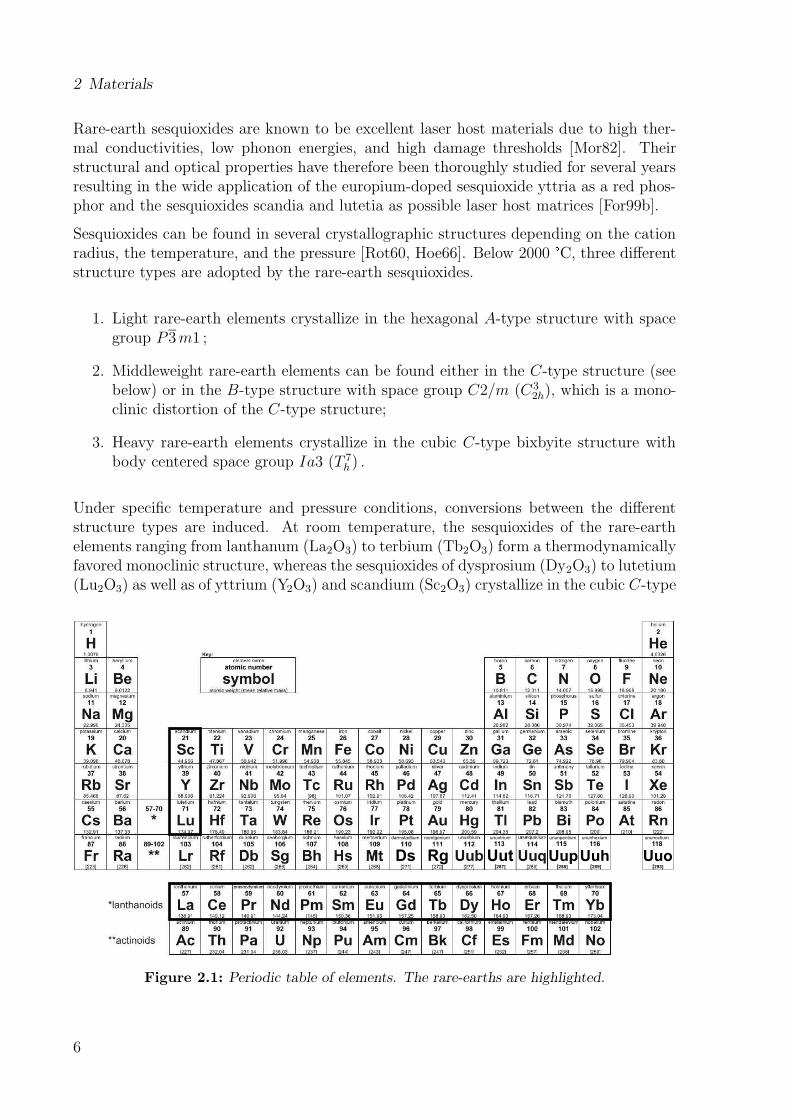
The term sesquioxide denotes oxide materials with an anion to cation ratio of 3 : 2 (lat.sesqui= one and a half). In the context of this thesis, however, when referring to sesquiox-ides, only the oxides of the rare-earth elements, which are found in the third main groupof the periodic table (cp. figure 2.1), will be considered.
Even though the rare-earth elements readily oxidize, they do so with varying strength[Hol92]. Cerium metal, in the presence of air, oxidizes completely to CeO2, whereaspraseodymium occurs naturally as Pr6O11, showing a slightly oxygen deficient fluoritestructure. The rare-earth oxides from neodymium onward all occur naturally as sesquiox-ides RE2O 3, except for terbium naturally occurring as Tb4O 7 and under positive oxygenpressure transforming into TbO2. However, only cerium, praseodymium and terbiumform dioxides1.1 Though still unclear why dioxides exist only for Ce, Pr, and Tb, the favoring of this structure can beexplained by the less tightly bound f electrons in the lighter lanthanides, resulting in compounds thatdisplay a larger oxygen coordination number. In terbium the extra electron on top of the half-filledshell is less tightly bound, resulting in a valency larger than 3+.
5
2 Materials
Rare-earth sesquioxides are known to be excellent laser host materials due to high ther-mal conductivities, low phonon energies, and high damage thresholds [Mor82]. Theirstructural and optical properties have therefore been thoroughly studied for several yearsresulting in the wide application of the europium-doped sesquioxide yttria as a red phos-phor and the sesquioxides scandia and lutetia as possible laser host matrices [For99b].
Sesquioxides can be found in several crystallographic structures depending on the cationradius, the temperature, and the pressure [Rot60, Hoe66]. Below 2000 � C, three differentstructure types are adopted by the rare-earth sesquioxides.
1. Light rare-earth elements crystallize in the hexagonal A-type structure with spacegroup P3m1 ;
2. Middleweight rare-earth elements can be found either in the C-type structure (seebelow) or in the B-type structure with space group C2/m (C3
2h), which is a mono-clinic distortion of the C-type structure;
3. Heavy rare-earth elements crystallize in the cubic C-type bixbyite structure withbody centered space group Ia3 (T 7
h ) .
Under specific temperature and pressure conditions, conversions between the differentstructure types are induced. At room temperature, the sesquioxides of the rare-earthelements ranging from lanthanum (La2O3) to terbium (Tb2O3) form a thermodynamicallyfavored monoclinic structure, whereas the sesquioxides of dysprosium (Dy2O3) to lutetium(Lu2O3) as well as of yttrium (Y2O3) and scandium (Sc2O3) crystallize in the cubic C-type
Ds Rg
darmstadtium roentgenium
Uut
ununtrium
Uup
ununpentium
Uuh
ununhexium
Uuo
ununoctium
113
[287]
115
[288]
116
[289]
118
[293]
Figure 2.1: Periodic table of elements. The rare-earths are highlighted.
6
2.1 Sesquioxides
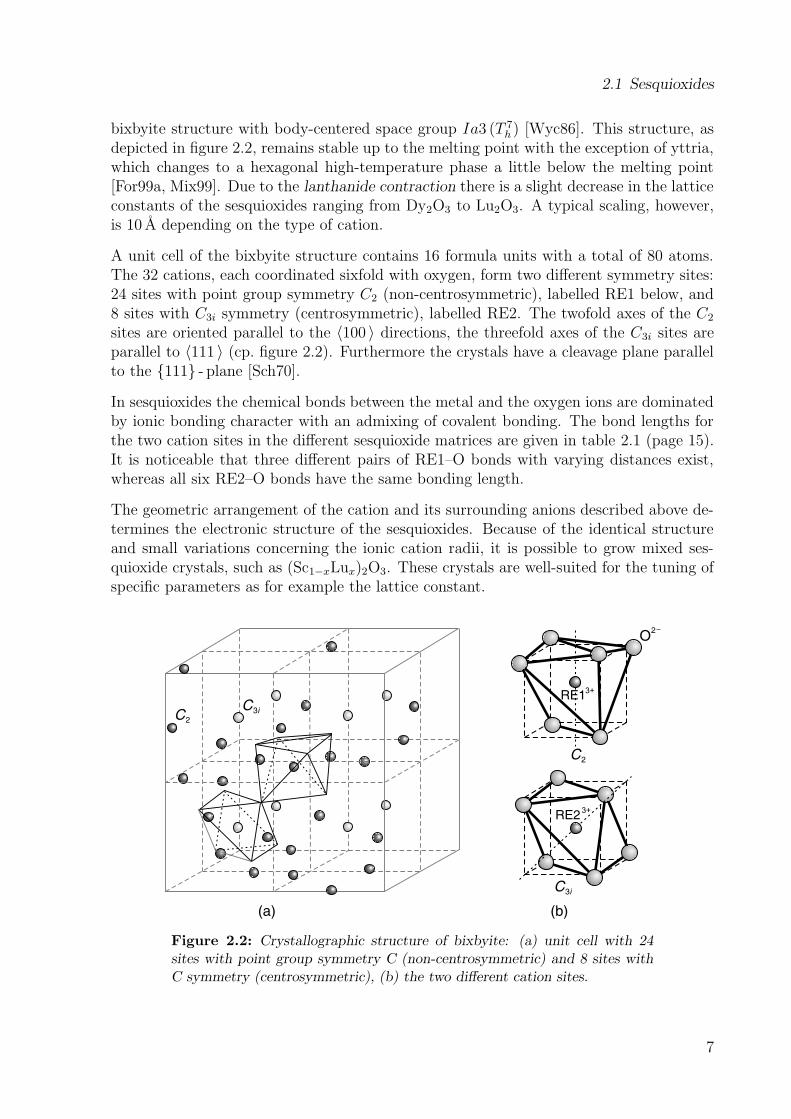
bixbyite structure with body-centered space group Ia3 (T 7h ) [Wyc86]. This structure, as
depicted in figure 2.2, remains stable up to the melting point with the exception of yttria,which changes to a hexagonal high-temperature phase a little below the melting point[For99a, Mix99]. Due to the lanthanide contraction there is a slight decrease in the latticeconstants of the sesquioxides ranging from Dy2O3 to Lu2O3. A typical scaling, however,is 10 A depending on the type of cation.
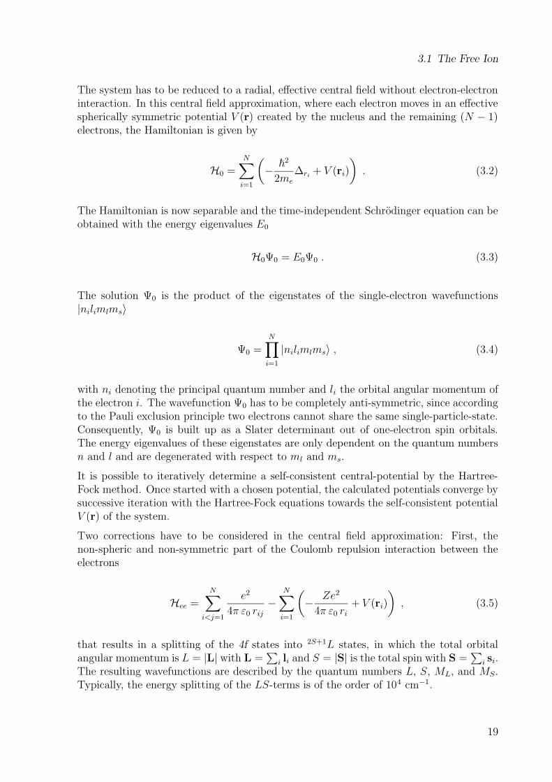
A unit cell of the bixbyite structure contains 16 formula units with a total of 80 atoms.The 32 cations, each coordinated sixfold with oxygen, form two different symmetry sites:24 sites with point group symmetry C2 (non-centrosymmetric), labelled RE1 below, and8 sites with C3i symmetry (centrosymmetric), labelled RE2. The twofold axes of the C2
sites are oriented parallel to the 〈100 〉 directions, the threefold axes of the C3i sites areparallel to 〈111 〉 (cp. figure 2.2). Furthermore the crystals have a cleavage plane parallelto the {111} - plane [Sch70].
In sesquioxides the chemical bonds between the metal and the oxygen ions are dominatedby ionic bonding character with an admixing of covalent bonding. The bond lengths forthe two cation sites in the different sesquioxide matrices are given in table 2.1 (page 15).It is noticeable that three different pairs of RE1–O bonds with varying distances exist,whereas all six RE2–O bonds have the same bonding length.
The geometric arrangement of the cation and its surrounding anions described above de-termines the electronic structure of the sesquioxides. Because of the identical structureand small variations concerning the ionic cation radii, it is possible to grow mixed ses-quioxide crystals, such as (Sc1−xLux)2O3. These crystals are well-suited for the tuning ofspecific parameters as for example the lattice constant.
(a) (b)
C2
C3i
C3i
O2
C2
RE13+
RE23+
Figure 2.2: Crystallographic structure of bixbyite: (a) unit cell with 24sites with point group symmetry C (non-centrosymmetric) and 8 sites withC symmetry (centrosymmetric), (b) the two different cation sites.
7
2 Materials
When activated with luminescent ions, the structural and electronic properties of thesesquioxides have important implications on the spectroscopic properties by determin-ing the crystal field and thus defining the energetic positions of the electronic states. Itwas found that, in general, trivalent rare-earth ions are randomly distributed in sesqui-oxide RE2O3 single-crystals, occupying different symmetry sites [Man63]. As a result ofthe differences between these two symmetry sites the spectroscopic characteristics of theRE3+(C2) and RE3+(C3i) ions differ from each other. The intraconfigurational f-f electricdipole transitions are forbidden for centrosymmetric C3i sites and only magnetic dipoletransitions can occur, whereas the crystal field interaction with non-centrosymmetric C2
sites introduces an opposite-parity part to the potential energy of the crystal levels, alsomaking possible the electric dipole transitions.
Compared with other dielectric oxide materials like YAlO3 or Y3Al5O12, sesquioxides havea considerably smaller phonon energy Eph = ~ωeff insuring good laser efficiency by min-imizing energy loss due to non-radiative processes. The phonon energy, already low inYAG with 700 cm−1, is even weaker in rare-earth oxides with 420 cm−1 for Gd2O3 and377 cm−1 for Y2O3. With non-radiative processes suppressed, this class of materials isinteresting for upconversion processes. However, up to now, besides the interest in theelectronic properties of crystalline yttria, no further investigation of the electronic struc-tures of scandia, lutetia or gadolinia are found in literature.
Growth of Sesquioxide Crystals
The main reason for sesquioxides not widely being used in industry is their complicatedgrowth. Unlike other materials of equal suitability as laser hosts, sesquioxide bulk crystalsor substrates are not commercially available up to now. Although sesquioxides, like yttria,are well investigated and their optical properties are quite favorable for laser applications,the extremely high melting point of approximately 2400 � C hinders the growth of large-volume single-crystals that are free of stress and impurities.
Until the end of the nineties experiments with various crystal growth techniques havebeen carried out, but none of them met the needs required for high-quality sesquioxides.Though, with these crystals grown, most properties of sesquioxides could be investigated.Then finally, much better results were obtained using a new growth method called heatexchange method (HEM) derived from the Bridgeman technique.
This technique was employed in the course of this work to grow sesquioxide bulk crystalswhich were then prepared as substrates for pulsed laser deposition and reference mea-surements. More information on the developed HEM growth technique and various othergrowth methods can be found in [Mix99, For99a, Pet01, Pet02a, Pet02b].
Yttrium-, Lutetium- and Scandiumoxide
Y2O3 is an insulator with a bandgap energy of approximately 6.1 eV [Abr78], meaningthat it is transparent up to the ultraviolet region of approximately 200 nm. Consequently,the absorption rises steeply at wavelengths smaller than 220 nm. The fundamental ab-sorption starts off with a sharp maximum at 5.9 eV, which is considered an excitonic state
8
2.1 Sesquioxides
[Abr78, Tom86]. As the short wavelength edge of the exciton band is superimposed bythe interband absorption, the binding energy of this exciton is considerably low (0.1 eV)[Abr78].
As self-consistent band structure calculations of Y2O3 by Xu et al. [Xu97] have shown,the upper valence band is mainly formed by 2p orbitals of oxygen electrons and someadmixing of yttrium 4d and 5p orbitals, whereas the lower conduction band states arepredominantly formed by yttrium 4d and 5p states. Based on the work of Ephraim andBloch [Eph26], who found that the values of the interelectronic repulsion parameters sep-arating the multiplet terms of 4f q (nephelauxetic effect, cp. page 18) are smaller in morecovalent compounds than in ionic compounds, and from the observed values of the inter-electronical repulsion parameters between the metal ion and the oxygen ligands, Jørgensenet al. predicted that a substantial degree of covalency is mixed with the predominant ionicbonding character between Y and O [Jør64]. The effective charges of Y1 and Y2 weredetermined to be +2.08 and +2.10, while the effective charge of the oxygen ions is −1.39[Xu97].
The sesquioxides Lu2O3 and Sc2O3 are isostructural to Y2O3. Consequently, the threecrystals are well comparable with regard to their optical properties. Lutetia shows areflectivity decrease related to interband transitions at an energy of 5.7 eV with a resultingbandgap energy of 6.1 eV. The excitonic state in lutetia is indicated via the sharp peakin the reflectivity spectrum at 5.8 eV [Kir03, Kuz03]. The valence band energy levelsin Y-based compounds are formed predominantly by oxygen 2p orbitals. However, inlutetia crystals the top of the valence band is composed mainly by lutetium 4f orbitals[Moi97]. Abramov et al. determined the bandgap energy of Sc2O3 to be 6.3 eV [Abr83]and performed additional calculations that indicated a predominance of the ionic bondand a slightly greater contribution of covalency compared to Y2O3 (qSc < qY).
One interesting difference between these three sesquioxides is the lack of an exciton de-tection for Sc2O3, whereas in Y2O3 as well as in Lu2O3 an excitonic state can be observed[Abr83]. However, due to the inconsistency of different literature values, uniformly mea-sured bandgap energies will be considered in this work. E. Mix determined the bandgapenergies of Sc2O3, Y2O3, and Lu2O3 to be 5.91 eV, 5.64 eV, and 5.51 eV, respectively[Mix99].
Gadoliniumoxide
The sesquioxide Gd2O3 differs from the others mentioned above. At room temperature itcrystallizes not in the C-type bixbyite structure but in the monoclinic B-type structurewith space group C2/m (C3
2h). This side-centered cell contains six fomula units withlattice constants having the values a = 14.08 A, b = 3.567 A, c = 8.743 A and β = 100 � .Lanthanide atoms are located in three non-equivalent sevenfold coordinated CS symmetrysites. Although the bandgap energy of Gd2O3 was investigated by Petit et al. to be5.3 eV [Pet05], more detailed information on the electronic structure was not available upto today.
9
2 Materials
In the context of this thesis Gd2O3 is not used as an isolated crystal but primarily asa compound of mixed sesquioxide (Gd1−xLux)2O3 crystals. Therefore the structure isconsidered cubic with the lattice constant value a = 10.813 A . This assumption is justifiedby X-ray measurements of the grown composite films (cp. section 9.1).
2.2 Corundum
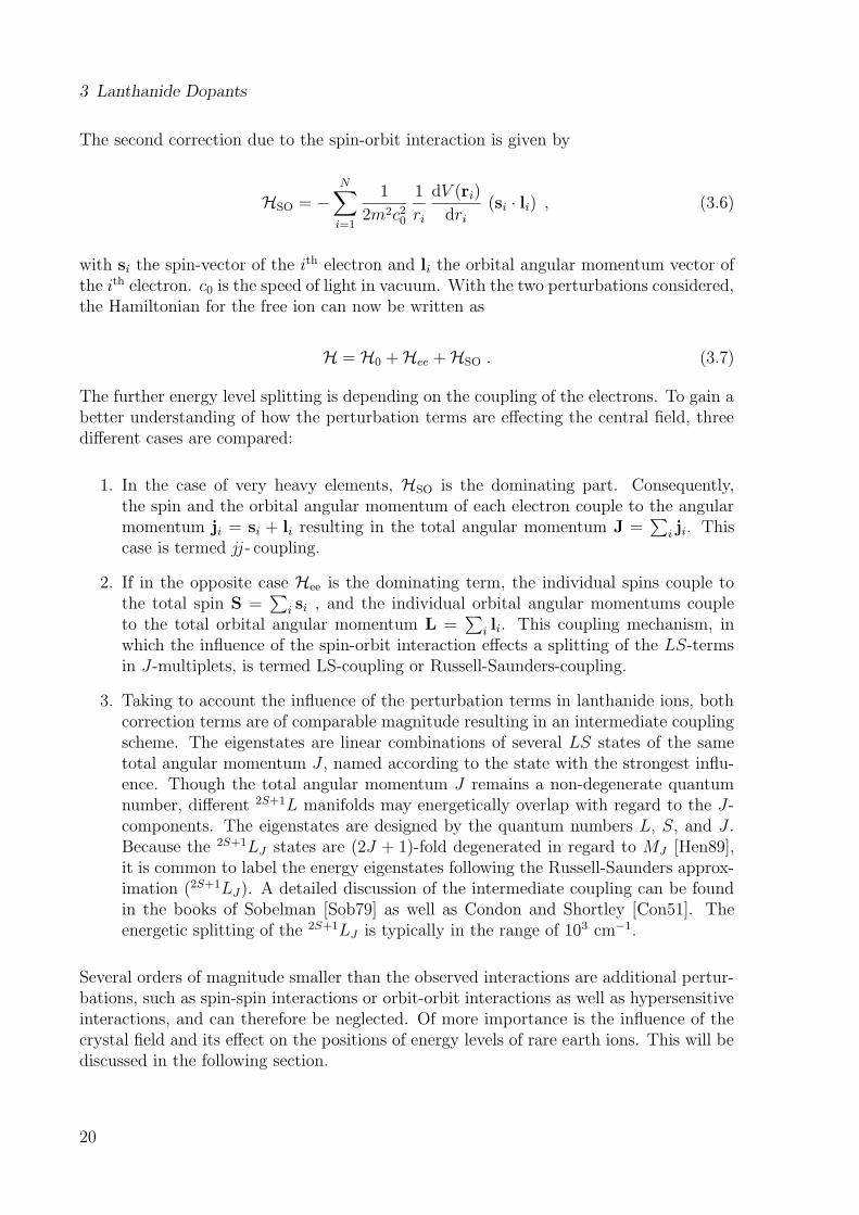
Depending on the conditions, aluminum oxide crystallizes in many different structures ofwhich the α-form (corundum) is the best known. This crystal is commercially availablein epitaxial high-quality with regard to crystal purity, precise orientation and surface pol-ishing. It is used as substrate material for pulsed laser deposition [Bur02, Bar04, Kuz06].Although the matrix itself is colorless, natural corundum often contains impurities caus-ing coloration. Pure α-Al2O3 is sometimes referred to as sapphire, despite the fact thatthe expression sapphire is more precisely defining Al2O3 doped with Fe2+ and Ti4+ re-sulting in blue colored crystals. With Cr3+ as dopant the crystal appears red and is
O2_
Al3+vacancy
a
b
c
Figure 2.3: Unit cell of α-alumina
commonly known as ruby. It is probably due to the vari-ous forms of Al2O3 in nature that the mineralogical termsapphire is widely used as a synonym for colorless pureα-Al2O3, alongside the term corundum.
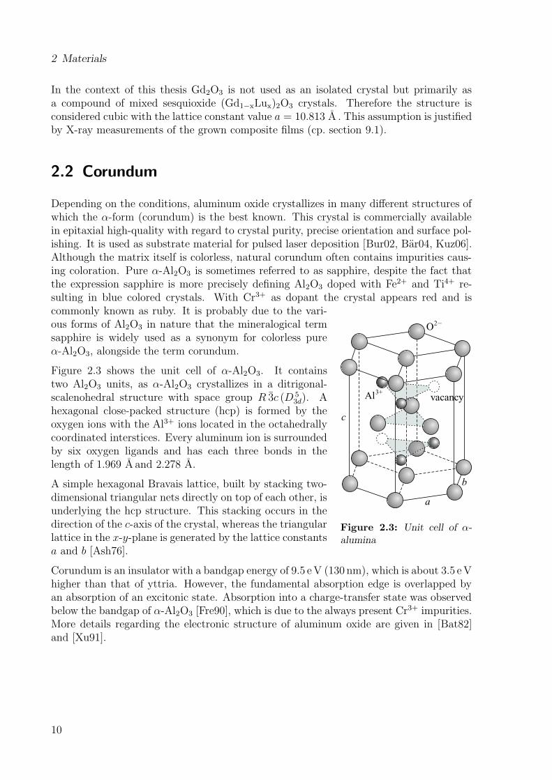
Figure 2.3 shows the unit cell of α-Al2O3. It containstwo Al2O3 units, as α-Al2O3 crystallizes in a ditrigonal-scalenohedral structure with space group R 3c (D 5
3d). Ahexagonal close-packed structure (hcp) is formed by theoxygen ions with the Al3+ ions located in the octahedrallycoordinated interstices. Every aluminum ion is surroundedby six oxygen ligands and has each three bonds in thelength of 1.969 A and 2.278 A.
A simple hexagonal Bravais lattice, built by stacking two-dimensional triangular nets directly on top of each other, isunderlying the hcp structure. This stacking occurs in thedirection of the c-axis of the crystal, whereas the triangularlattice in the x-y-plane is generated by the lattice constantsa and b [Ash76].
Corundum is an insulator with a bandgap energy of 9.5 eV (130 nm), which is about 3.5 eVhigher than that of yttria. However, the fundamental absorption edge is overlapped byan absorption of an excitonic state. Absorption into a charge-transfer state was observedbelow the bandgap of α-Al2O3 [Fre90], which is due to the always present Cr3+ impurities.More details regarding the electronic structure of aluminum oxide are given in [Bat82]and [Xu91].
10
2.3 Yttrium Aluminum Garnet
2.3 Yttrium Aluminum Garnet
Favorable spectroscopic properties, high thermal conductivity, mechanical stability, andhigh optical damage threshold were some of the features that made yttrium aluminumgarnet one of the most important host materials for laser application. Many commerciallyproduced solid-state lasers are based on this material, referred to as YAG. Up to now,well-known laser performances have been obtained by rare-earth-doped YAG crystals,such as Nd:YAG and Yb:YAG.
It was Menzer who in 1928 pioneered the investigating of this new material class, laternamed garnets [Men28]. The crystals categorized in this class belong to the cubic, body-centered space group Ia3d (O 10
h ).
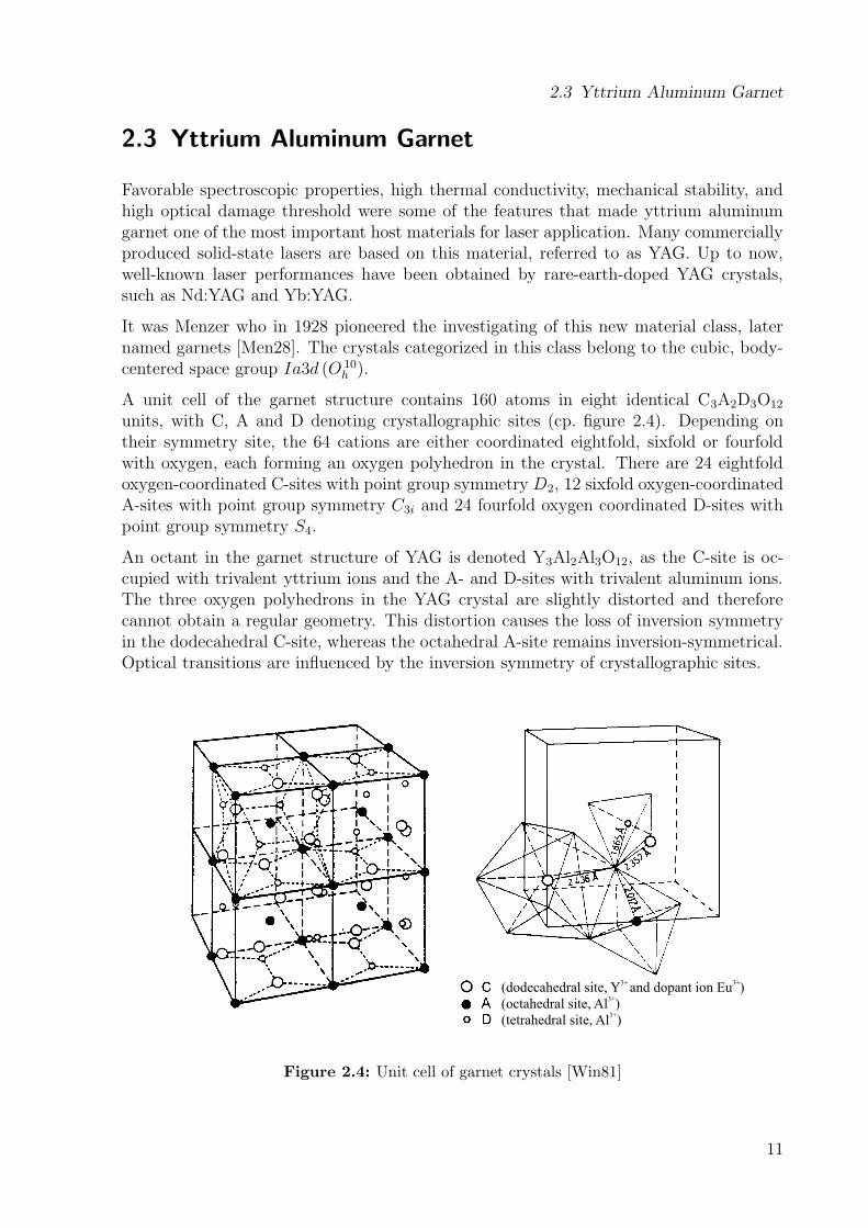
A unit cell of the garnet structure contains 160 atoms in eight identical C3A2D3O12
units, with C, A and D denoting crystallographic sites (cp. figure 2.4). Depending ontheir symmetry site, the 64 cations are either coordinated eightfold, sixfold or fourfoldwith oxygen, each forming an oxygen polyhedron in the crystal. There are 24 eightfoldoxygen-coordinated C-sites with point group symmetry D2, 12 sixfold oxygen-coordinatedA-sites with point group symmetry C3i and 24 fourfold oxygen coordinated D-sites withpoint group symmetry S4.
An octant in the garnet structure of YAG is denoted Y3Al2Al3O12, as the C-site is oc-cupied with trivalent yttrium ions and the A- and D-sites with trivalent aluminum ions.The three oxygen polyhedrons in the YAG crystal are slightly distorted and thereforecannot obtain a regular geometry. This distortion causes the loss of inversion symmetryin the dodecahedral C-site, whereas the octahedral A-site remains inversion-symmetrical.Optical transitions are influenced by the inversion symmetry of crystallographic sites.
(dodecahedral site, Y and dopant ion Eu )
(octahedral site, Al )
(tetrahedral site, Al )
3+ 3+
3+
3+
Figure 2.4: Unit cell of garnet crystals [Win81]
11
2 Materials
YAG is an insulator with a bandgap energy of 6.5 eV. Calculations of its electronicstructure were performed recently by Xu and Ching [Xu99, Chi99].
One can also consider YAG as a congruent mixture of two oxides – Y2O3 and Al2O3.Other congruent compositions of the same compounds are YAlO3 (YAP) with a perovskiteorthorhombic lattice and Y4Al2O9 (YAM) with a monoclinic structure. Although YAP issometimes utilized as a host for rare-earth dopants, both, YAP and YAM, are not widelyused.
2.4 Orthovanadates of Yttrium and Gadolinium
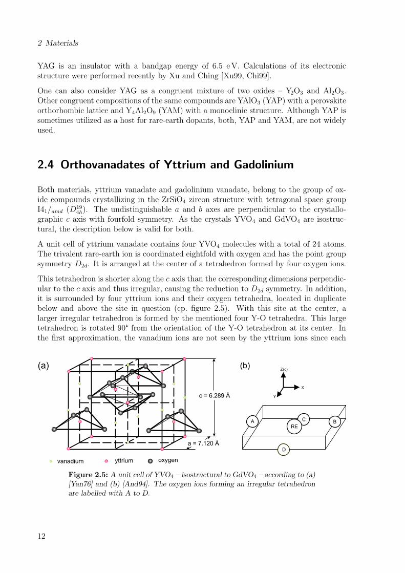
Both materials, yttrium vanadate and gadolinium vanadate, belong to the group of ox-ide compounds crystallizing in the ZrSiO4 zircon structure with tetragonal space groupI41/amd (D19
4h). The undistinguishable a and b axes are perpendicular to the crystallo-graphic c axis with fourfold symmetry. As the crystals YVO4 and GdVO4 are isostruc-tural, the description below is valid for both.
A unit cell of yttrium vanadate contains four YVO4 molecules with a total of 24 atoms.The trivalent rare-earth ion is coordinated eightfold with oxygen and has the point groupsymmetry D2d. It is arranged at the center of a tetrahedron formed by four oxygen ions.
This tetrahedron is shorter along the c axis than the corresponding dimensions perpendic-ular to the c axis and thus irregular, causing the reduction to D2d symmetry. In addition,it is surrounded by four yttrium ions and their oxygen tetrahedra, located in duplicatebelow and above the site in question (cp. figure 2.5). With this site at the center, alarger irregular tetrahedron is formed by the mentioned four Y-O tetrahedra. This largetetrahedron is rotated 90 � from the orientation of the Y-O tetrahedron at its center. Inthe first approximation, the vanadium ions are not seen by the yttrium ions since each
(a)
yttrium oxygenvanadium
c = 6.289 Å
a = 7.120 Å
REA C
D
B
Z(c)
Y
X
(b)
Figure 2.5: A unit cell of YVO4 – isostructural to GdVO4 – according to (a)[Yan76] and (b) [And94]. The oxygen ions forming an irregular tetrahedronare labelled with A to D.
12
2.5 Lithium Yttrium Fluoride
vanadium ion, due to its small size of 0.59 A , is completely shielded by a tetrahedron ofoxygen ions [Yan76].
The lattice constants of YVO4 have the values a = 7.120 A and c = 6.289 A . In com-parison, replacing trivalent yttrium ions by larger gadolinium ions increases the distancesbetween dodecahedral lattice sites, causing a decrease of ion-ion interaction between neigh-boring ions and also making the segregation coefficient closer to unity. The lattice pa-rameters of GdVO4 are a = 7.211 A and c = 6.350 A .
2.5 Lithium Yttrium Fluoride
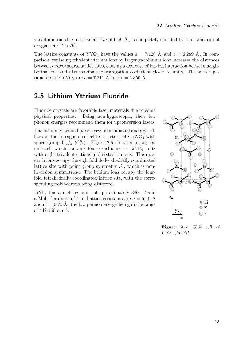
a
a
c
Li
Y
F
Figure 2.6: Unit cell ofLiYF4 [Win81]
Fluoride crystals are favorable laser materials due to somephysical properties. Being non-hygroscopic, their lowphonon energies recommend them for upconversion lasers.
The lithium yttrium fluoride crystal is uniaxial and crystal-lizes in the tetragonal scheelite structure of CaWO4 withspace group I41/a (C6
4h). Figure 2.6 shows a tetragonalunit cell which contains four stoichiometric LiYF4 unitswith eight trivalent cations and sixteen anions. The rare-earth ions occupy the eightfold dodecahedrally coordinatedlattice site with point group symmetry S4, which is non-inversion symmetrical. The lithium ions occupy the four-fold tetrahedrally coordinated lattice site, with the corre-sponding polyhedrons being distorted.
LiYF4 has a melting point of approximately 840 � C anda Mohs hardness of 4-5. Lattice constants are a = 5.16 Aand c = 10.75 A , the low phonon energy being in the rangeof 442-460 cm−1.
13
2 Materials
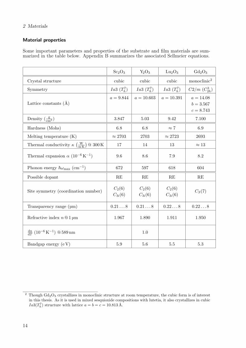
Material properties
Some important parameters and properties of the substrate and film materials are sum-marized in the table below. Appendix B summarizes the associated Sellmeier equations.
Sc2O3 Y2O3 Lu2O3 Gd2O3
Crystal structure cubic cubic cubic monoclinic2
Symmetry Ia3 (T 7h ) Ia3 (T 7
h ) Ia3 (T 7h ) C2/m (C3
2h)
Lattice constants (A)a = 9.844 a = 10.603 a = 10.391 a = 14.08
b = 3.567
c = 8.743
Density ( gcm3 ) 3.847 5.03 9.42 7.100
Hardness (Mohs) 6.8 6.8 ≈ 7 6.9
Melting temperature (K) ≈ 2703 2703 ≈ 2723 2693
Thermal conductivity κ(WmK
)@ 300K 17 14 13 ≈ 13
Thermal expansion α (10−6K−1) 9.6 8.6 7.9 8.2
Phonon energy ~ωmax (cm−1) 672 597 618 604
Possible dopant RE RE RE RE
Site symmetry (coordination number)C2(6) C2(6) C2(6) CS(7)C3i(6) C3i(6) C3i(6)
Transparency range ( � m) 0.21 . . . 8 0.21 . . . 8 0.22 . . . 8 0.22 . . . 8
Refractive index n@1 � m 1.967 1.890 1.911 1.950
dndT (10
−6K−1) @ 589 nm 1.0
Bandgap energy (eV) 5.9 5.6 5.5 5.3
2 Though Gd2O3 crystallizes in monoclinic structure at room temperature, the cubic form is of interestin this thesis. As it is used in mixed sesquioxide compositions with lutetia, it also crystallizes in cubicIa3(T 7
h ) structure with lattice a = b = c = 10.813 A.
14
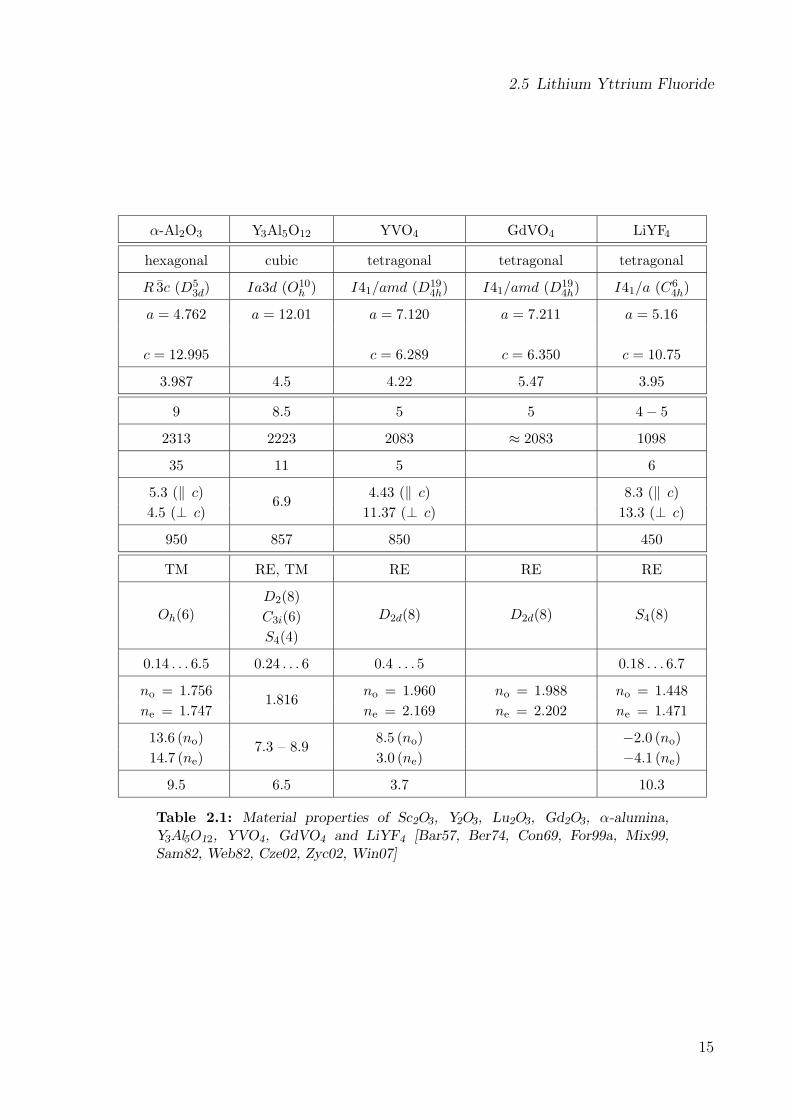
2.5 Lithium Yttrium Fluoride
α-Al2O3 Y3Al5O12 YVO4 GdVO4 LiYF4
hexagonal cubic tetragonal tetragonal tetragonal
R 3c (D53d) Ia3d (O10
h ) I41/amd (D194h) I41/amd (D19
4h) I41/a (C64h)
a = 4.762 a = 12.01 a = 7.120 a = 7.211 a = 5.16
c = 12.995 c = 6.289 c = 6.350 c = 10.75
3.987 4.5 4.22 5.47 3.95
9 8.5 5 5 4− 52313 2223 2083 ≈ 2083 1098
35 11 5 6
5.3 (‖ c)6.9
4.43 (‖ c) 8.3 (‖ c)
4.5 (⊥ c) 11.37 (⊥ c) 13.3 (⊥ c)
950 857 850 450
TM RE, TM RE RE RE
Oh(6)D2(8)
D2d(8) D2d(8) S4(8)C3i(6)
S4(4)
0.14 . . . 6.5 0.24 . . . 6 0.4 . . . 5 0.18 . . . 6.7
no = 1.7561.816
no = 1.960 no = 1.988 no = 1.448
ne = 1.747 ne = 2.169 ne = 2.202 ne = 1.471
13.6 (no) 7.3 – 8.98.5 (no) −2.0 (no)
14.7 (ne) 3.0 (ne) −4.1 (ne)9.5 6.5 3.7 10.3
Table 2.1: Material properties of Sc2O3, Y2O3, Lu2O3, Gd2O3, α-alumina,Y3Al5O12, YVO4, GdVO4 and LiYF4 [Bar57, Ber74, Con69, For99a, Mix99,Sam82, Web82, Cze02, Zyc02, Win07]
15

2 Materials
16
3 Lanthanide Dopants
In order to study the properties of thin films, lanthanide ions are used as luminescentprobes. This is due to the sensitivity of their emission characteristics to the crystallo-graphic environment. Electronic transitions and characteristic optical properties of rare-earth ions, reviewed in this chapter, are required to interpret the optical data of thepresented systems. When introduced by substitution of another non-luminescent unit, itis essential that the probe perturbs the investigated material as little as possible.
The elements used for doping can be found in the third main group of the periodic table(cp. figure 2.1). First introduced in this work in section 2.1, the term rare-earth (RE)usually refers to the elements lanthanum (atomic no. 57) through lutetium (atomic no. 71)also known as lanthanides, and the chemically similar elements scandium (atomic no. 21)and yttrium (atomic no. 39) [Gre87]. However, the following discussion will only addressthe lanthanides.
As also known from other element groups in the periodic table, the lanthanides of in-creasing atomic number show a periodic behavior with regard to some of their properties,like density, melting and boiling points, while other properties, like ionic radii, changeaperiodically. This aperiodic phenomenon is referred to as lanthanide contraction.
The similarity in chemical properties stems from the electron configuration of rare-earthatoms, denoted1 [Xe] (4f )n(5d)x(6s)2 with x = 1 in the case of lanthanum (n = 0), gadolin-ium (n = 7), lutetium (n = 14) and x = 0 with n = 2 through n = 14 for cerium throughytterbium. Although the incorporation of the rare-earth ions into a crystal matrix uses thestable trivalent form with the electron configuration [Xe] (4f )n+x−1, divalent rare-earthscan appear in crystals with divalent lattice sites. Another occasion for divalent rare-earthions is local charge compensation provided either by crystal defects, such as color centersin sesquioxides and garnets, or by the presence of quadrivalent co-dopants in the crystalmatrix [Kap62, Loh69].
1 [Xe] represents the electron configuration of the noble gas xenon.
17
3 Lanthanide Dopants
The spectroscopic properties of the trivalent rare-earth atoms are dominated by intra-configurational 4f-4f transitions and interconfigurational 4f-5d transitions. Because the 5sand 5p shells are completely filled in the [Xe] configuration, the 4f shell electrons are effec-tively shielded from influences of the chemical environment, e. g. the surrounding crystalfield. Therefore, only low variations of the 4f states can be observed in different localenvironments [Bur62, Ray63]. This insensitivity to the surrounding offers the advantageof easily determining the energy levels by adding the influence of the crystal field as aperturbation to the free ion energy level terms. In case of the investigated 4f-4f electricdipole transitions, this results in narrow transition line-widths, compared to those ob-served in transition metals, in divalent rare-earths, and between RE3+ 5d states [Hen89].The strength of the shielding decreases with increasing atomic numbers [Ste66, Erd72].
Due to the influence of the crystal matrix, the peak positions of the 4f-4f transitionsperform a little shift. This behavior is known as the nephelauxetic effect (Greek: cloudexpanding). As interelectronic repulsion and spin-orbit coupling primarily determine theenergies of the excited levels, a shift of the peak positions towards lower energy withincreasing covalency of the surrounding media is expected. This behavior recommendsthe rare-earths as suitable probe ions, which is also due to the crystallographic propertiesof their lattice sites. A detailed discussion of the nephelauxetic effect is given in [Sin66].
Aside from europium, which can be used as a red light emitter in phosphors and is utilizedas the main probe ion within the context of this thesis, there are also other rare-earthsthat are very promising as dopant ions for sesquioxides. Neodymium doping in scandiafor operation at 1486 nm is recommendable for the telecommunications industry whileerbium in lutetia may prove to be suitable for high power operation at 2.7 � m in medicalapplications [Pet01]. Besides, high power laser operation was recently demonstrated withYb:Lu2O3 and Yb:Sc2O3 in a thin-disk laser geometry [Pet07].
3.1 The Free Ion
In order to calculate the electronic states together with their energies, the Hamiltonianmust be determined and the Schrodinger equation solved. For a free ion with a nucleusof charge Ze and N electrons of mass me the Hamiltonian is
H =N∑
i=1
(
− ~2
2me
∆ri −Ze2
4πε0ri
)
+N∑
i<j=1
e2
4πε0rij. (3.1)
The kinetic energy of the electrons −(~2∆ri/2me) as well as their Coulomb interaction−(Ze2/4πε0ri) with the nucleus is described in the first summation. The distance betweenthe electron i and the nucleus is denoted ri. Represented in the second summation isthe electrostatic repulsion between the electrons which are separated by the distancerij = |ri − rj|. Obviously, a separation of the Schrodinger equation in N one-particle-problems is not possible because of this two-particle-operator, and hence no analyticalsolution can be found.
18
3.1 The Free Ion
The system has to be reduced to a radial, effective central field without electron-electroninteraction. In this central field approximation, where each electron moves in an effectivespherically symmetric potential V (r) created by the nucleus and the remaining (N − 1)electrons, the Hamiltonian is given by
H0 =N∑
i=1
(
− ~2
2me
∆ri + V (ri)
)
. (3.2)
The Hamiltonian is now separable and the time-independent Schrodinger equation can beobtained with the energy eigenvalues E0
H0Ψ0 = E0Ψ0 . (3.3)
The solution Ψ0 is the product of the eigenstates of the single-electron wavefunctions|nilimlms〉
Ψ0 =N∏
i=1
|nilimlms〉 , (3.4)
with ni denoting the principal quantum number and li the orbital angular momentum ofthe electron i. The wavefunction Ψ0 has to be completely anti-symmetric, since accordingto the Pauli exclusion principle two electrons cannot share the same single-particle-state.Consequently, Ψ0 is built up as a Slater determinant out of one-electron spin orbitals.The energy eigenvalues of these eigenstates are only dependent on the quantum numbersn and l and are degenerated with respect to ml and ms.
It is possible to iteratively determine a self-consistent central-potential by the Hartree-Fock method. Once started with a chosen potential, the calculated potentials converge bysuccessive iteration with the Hartree-Fock equations towards the self-consistent potentialV (r) of the system.
Two corrections have to be considered in the central field approximation: First, thenon-spheric and non-symmetric part of the Coulomb repulsion interaction between theelectrons
Hee =N∑
i<j=1
e2
4π ε0 rij−
N∑
i=1
(
− Ze2
4π ε0 ri+ V (ri)
)
, (3.5)
that results in a splitting of the 4f states into 2S+1L states, in which the total orbitalangular momentum is L = |L| with L =
∑
i li and S = |S| is the total spin with S =∑
i si.The resulting wavefunctions are described by the quantum numbers L, S, ML, and MS.Typically, the energy splitting of the LS-terms is of the order of 104 cm−1.
19
3 Lanthanide Dopants
The second correction due to the spin-orbit interaction is given by
HSO = −N∑
i=1
1
2m2c20
1
ri
dV (ri)
dri(si · li) , (3.6)
with si the spin-vector of the ith electron and li the orbital angular momentum vector ofthe ith electron. c0 is the speed of light in vacuum. With the two perturbations considered,the Hamiltonian for the free ion can now be written as
H = H0 +Hee +HSO . (3.7)
The further energy level splitting is depending on the coupling of the electrons. To gain abetter understanding of how the perturbation terms are effecting the central field, threedifferent cases are compared:
1. In the case of very heavy elements, HSO is the dominating part. Consequently,the spin and the orbital angular momentum of each electron couple to the angularmomentum ji = si + li resulting in the total angular momentum J =
∑
i ji. Thiscase is termed jj - coupling.
2. If in the opposite case Hee is the dominating term, the individual spins couple tothe total spin S =
∑
i si , and the individual orbital angular momentums coupleto the total orbital angular momentum L =
∑
i li. This coupling mechanism, inwhich the influence of the spin-orbit interaction effects a splitting of the LS-termsin J-multiplets, is termed LS-coupling or Russell-Saunders-coupling.
3. Taking to account the influence of the perturbation terms in lanthanide ions, bothcorrection terms are of comparable magnitude resulting in an intermediate couplingscheme. The eigenstates are linear combinations of several LS states of the sametotal angular momentum J , named according to the state with the strongest influ-ence. Though the total angular momentum J remains a non-degenerate quantumnumber, different 2S+1L manifolds may energetically overlap with regard to the J-components. The eigenstates are designed by the quantum numbers L, S, and J .Because the 2S+1LJ states are (2J + 1)-fold degenerated in regard to MJ [Hen89],it is common to label the energy eigenstates following the Russell-Saunders approx-imation (2S+1LJ). A detailed discussion of the intermediate coupling can be foundin the books of Sobelman [Sob79] as well as Condon and Shortley [Con51]. Theenergetic splitting of the 2S+1LJ is typically in the range of 103 cm−1.
Several orders of magnitude smaller than the observed interactions are additional pertur-bations, such as spin-spin interactions or orbit-orbit interactions as well as hypersensitiveinteractions, and can therefore be neglected. Of more importance is the influence of thecrystal field and its effect on the positions of energy levels of rare earth ions. This will bediscussed in the following section.
20
3.2 The Lanthanide Ion in a Crystal Matrix
3.2 The Lanthanide Ion in a Crystal Matrix
When an ion is incorporated into a crystal lattice – any other chemical environment likeglass or solution will also do –, it is subject to the electrostatic field of the neighboringions, also called ligands. By the interaction of the 4f electrons of a lanthanide ion withthe mentioned electrostatic field of the ligands, the spherical symmetry of the free ion isdestroyed. This is referred to as Stark effect. The influence of the local electric field Eintroduced as an additional perturbation term is represented by the Hamiltonian
HStark = −eN∑
k=1
E(rk) · rk . (3.8)
The crystal field has two effects on the energy level structure of the free ion.
1. It induces a red shift on the free ion levels that can be explained by a reduction ofthe free ion parameters [Jør77] referred to as nephelauxetic effect (cp. page 18).
2. It causes a Stark splitting of the 2S+1LJ manifolds of the free ion and thus repealsthe degeneracy with respect to MJ . For lanthanide ions having an odd number ofelectrons, the Kramers theorem asserts a splitting in (2J + 1)/2 twofold degener-ated Stark levels. This Kramers degeneration is a consequence of the time-reversalinvariance. Ions with an even number of electrons are split into (2J + 1) levels[Mes90].
The Hamiltonian for a rare-earth ion arranged in a crystal field is concludingly given by
H = H0 +Hee +HSO +HStark , (3.9)
with the influence of the perturbation HStark being one order of magnitude smaller thanthe contributions of HSO and Hee, as the 4f electrons are shielded from the crystal field bythe 5s and 5p electrons. As the interaction with the ligand field or with vibrational statesmixes electronic states of different parity into the 4f-wavefunctions, the regularly forbiddenelectric dipole transitions within the 4f shell are now partially allowed (cp. section 3.2.1).
21
3 Lanthanide Dopants
3.2.1 Intraconfigurational 4f-4f Transitions
The excitation of an ion via an electron transition from the ground state to a higher energylevel can be initiated by an oscillating electromagnetic field of appropriate frequency. Ashigher order transitions like electric or magnetic quadrupole processes can generally beneglected due to reduced transition probabilities [Die68, Pea75], the transitions betweentwo energy levels may be categorized in having either electric dipole or magnetic dipolecharacter.
In expressing the electric field in terms of a multipole expansion, the first terms of ordern of this expansion are denoted monopole (n = 0), dipole (n = 1), quadrupole (n = 3),and octupole (n = 4). The Laporte selection rules for electric multipole transitions oforder n in a symmetric central field are:
1. For n = 0, 2, 4, . . . only transitions between states of the same parity are allowed.
2. For n = 1, 3, 5, . . . only transitions between states of different parity are allowed.
As electric dipole transitions require a change of parity of the electron wavefunction,they are forbidden within the 4f shell, due to the Laporte selection rules above, and onlymagnetic dipole transitions are expected [Hen89]. Usually these transitions are weakerthan electric dipole transitions by a factor of 105.
However, under the influence of crystal fields without inversion symmetry, a configura-tional mixing of opposite-parity states – like 4f n-15d – into the 4f n states can occur partlyallowing electron dipole transitions in the 4f states and retensioning the Laporte rules.In the case of crystallographic sites with inversion symmetry the Laporte selection ruleis weakened by rare-earth ions occupying acentric sites in the matrix, reintroducing in-traconfigurational 4f-4f transitions observed as forced electric dipole transitions. Though,the weakening of inversion symmetrical sites is considerably smaller than of non-inversionsites. The selection rules for these forced electric dipole transitions between 4f n states are[Hen89, Kam90]
1. ∆l = ±1 3. ∆L = 2 l = 6
2. ∆S = 0 4. ∆J = 2 l = 6
In the case of rare-earth ions with an even number of electrons some additional selectionrules apply as follows
1. J = 0 ↔ J ′ = 0 forbidden
2. J = 0 ↔ J ′ = 2, 4, 6, . . . strong
3. J = 0 ↔ J ′ = 1, 3, 5, . . . weak .
Intensive investigation on the admixing of states with opposite parity to the 4f states wasdone by Judd and Ofelt [Jud62, Ofe62].
As mentioned earlier, two different lattice sites with symmetry C2 and symmetry C3i
are provided by the matrix of the sesquioxides (cp. chapter 2.1). As the C3i-sites show
22
3.2 The Lanthanide Ion in a Crystal Matrix
inversion symmetry, the effect of admixing is considerably smaller compared to the C2-sites, due to the lack of a center symmetry. Thus, the Laporte selection rule is stronger forions occupying the C3i-site, resulting in a reduced transition probability compared withtransitions of ions in the C2-site.
After having described the intraconfigurational, parity forbidden 4f-4f-transitions (weak)and the applying selection rules, we will now focus on the parity allowed transitions of thelanthanide ions (strong), which appear as broad bands in optical spectra. These parityallowed transitions are the interconfigurational 4f n → 4f n−15d and the charge transfer(CT) transitions.
3.2.2 Interconfigurational 4f-5d Transitions
The outer electrons situated in the 5d-orbitals are not shielded by other electrons as theones in the 4f-levels and therefore energetically very sensitive to the environment. Thus,the crystal field is the primary influence of these 5d-orbitals, being more relevant thanthe Stark effect or the Coulomb interaction [Loh73]. The position of the energy levels andthe splitting due to the crystal field with respect to the site symmetry [Sch67] is given bythe ligand-field theory.
This model contributes an extension to the crystal field theory to allow covalent interac-tions and is valid for electrons in non-completely filled shells. The bonding is generallyexplained by molecular orbital theory [Sch67, Sch73, Bal62].
Assumptions regarding the ligand field theory are that the motion of the electrons occursin the potential of the metal ion core as well as in the electrostatic potential of the ligands.The interaction among the electrons of the central ion and the electrons of the ligandscan be neglected, as the ligands are regarded as point charges. The energy splitting istherefore explained as a consequence of this electrostatic interaction, with the premise ofpurely ionic bonding between the metal ion and the ligands having no covalent admixture.
The orientation of the d-orbital wavefunctions either increases or decreases the electronenergy depending on the orbital extended into a region of high or low electron density.This results in a splitting of energy levels.
Applying this electrostatic model for example to an octahedrally coordinated d1 electronwhich is – due to the angular part of the crystal field potential – degenerated twofold inan Eg state and threefold in a T2g state, the energy difference of the splitting is given by
10DqOkt =q〈r4〉6R5
. (3.10)
The total energy splitting 10Dq is named crystal field stabilization energy, with 〈r〉 beingthe radial probability density of the electron and R the metal-ligand internuclear distance.Because of the destabilizing effect of the center symmetrical part of the ligand field, anenergetic increase ε0, Okt is induced on the d1 electron levels, with the resulting influenceof the ligand field on a single d1 electron of
23
3 Lanthanide Dopants
∆εOkt = ε0, Okt +
{+6DqOkt for Eg
−4DqOkt for T2g
. (3.11)
It has to be mentioned though, that the excitation of an 4f electron into a 5d orbitalpresents a 4f n → 4f n−15d transition and thus cannot be described as a one-particle-problem. All electrons, 4f and 5d orbitals have to be taken into account in order to obtainan exact calculation of the energy levels.
In general, a large crystal field splitting energy is provided by ligands with high negativecharge and small radius and by metal cations with large oxidation number. In section 3.2.4a more illustrative description of the 4f-5d transitions is given, as the single configurationalcoordinate model is introduced.
3.2.3 Charge Transfer Transitions
Interconfigurational transitions which involve a ligand-to-metal charge transfer transitionand the reverse process, a metal-to-ligand charge transfer transition, are referred to ascharge transfer transitions. An electronic state in which a large fraction of the electroniccharge is transferred from one molecular entity (electron donor) to another (electronacceptor) is generally defined as charge transfer state (CTS) [McN97]. The charge centerbetween the central ion and the ligands is considerably shifted with respect to the groundstate. This is due to the displacement of electronic charge across a typical interatomicdistance. The shifted charge center produces a large transition dipole moment and aconcomitant large oscillator strength.
An often given description of a ligand-to-metal charge transfer process is the transfer of anelectron from the ligands to the central metal ion (Mn+Lm− → M(n−1)+L(m−1)−) resultingin an excitation of an electronic state, which is called charge transfer state [Pie01]. Thismodel then interprets a charge transfer state as a hole which is transferred from the RE3+
ion to the ligands, moving around the RE2+ core in a potential field produced by thelattice because of the effective negative charge [Hos77].
The energy of a charge transfer band ECT is dependent on the donor ionization energy, theacceptor electron affinity and on the extent of the charge displacement. As the CT bandenergy correlates well with the Pauling scale of electronegativities, Jørgensen introducedthe concept of optical electronegativity [Jør70]. According to this model, the energy ECT
can be estimated by the optical electronegativity of the anion χopt(L) and of the centralmetal ion χopt(M) as follows:
ECT = [χopt(L)− χopt(M)]× 30 000 cm−1 . (3.12)
For the corresponding values χopt(Eu3+) = 1.8 and χopt(O
2−) = 3.2 of the investigatedEu3+ ion in an oxide host matrix, the average CT band position equals 42 000 cm−1,being anti-proportional to the Eu-O distance. The band shifts to lower energies withincreasing bond length [Hoe75].
24
3.2 The Lanthanide Ion in a Crystal Matrix
D05
FJ7
ener
gyE
CTS
Q0(CTS) Q
Q0(4 )f
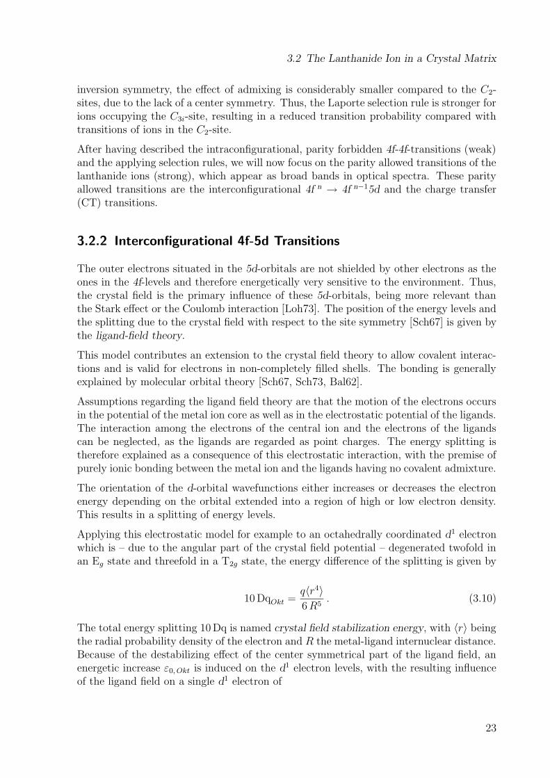
Figure 3.1: CT excitation of Eu3+:Y2O3
The involvement of a charge transfer state ineither absorption or emission processes canbe observed. However, luminescence from acharge transfer state is only possible if thisstate is lower in energy than the lowest en-ergy level of an excited 4f n−15d state. More-over, no 4f energy levels are allowed to bepresent at energies comparable to the chargetransfer state, because of the resulting fastintersystem crossing to the lower energy 4f n
states and 4f n → 4f n emission. In figure 3.1this mechanism is shown for Eu3+:Y2O3 andthe case that UV radiation is efficiently ab-sorbed by a transition to the charge transferstate of the Eu3+ ion. No emission is takingplace from the charge transfer state, becauseof the relaxation to the lower 4f levels in the5DJ manifold. Instead, luminescence fromthe 5D0 state of Eu3+ occurs [Nak79].
3.2.4 Vibrations of the Host Lattice
Host lattice vibrations have significant influence on the optical transitions of the rare-earth ions. Again, it is necessary to expand the Hamiltonian operator of two additionalterms in order to describe the electron-phonon interactions. The first considers the kineticenergy of all ions and the second takes into account the interionic potential energy dueto the movements off the equilibrium positions.
In comparison, the electron-phonon coupling of the 5d electrons is significantly strongerthan the one of the 4f electrons because of the wider ranging radial expansion and un-shielded interaction of the 5d orbitals. While the 4f-4f transitions are quite narrow banded,the electron-phonon interaction leads to a strong broadening of the interconfigurationaltransitions.
A more illustrative description of these phenomenons is given by the single-configurationalcoordinate model [Bar74, Hen89]. In this model radiative and non-radiative transitions,the shape of an optical transition (narrow or broad lines), as well as the Stokes’ Law areexplained. It is based on the Born-Oppenheimer approximation [Bor27], separating themotion of the electrons from the one of the nuclei (lattice vibrations). The eigenvaluesφ(ri, Rl) of the electron-phonon coupling can be written be
φ(ri, Rl) = ψ(ri)χ(Rl) , (3.13)
with the position of the lth ion Rl, the electronic part ψ(ri) describing the eigenvalues ofthe Hamilton operator in a static lattice and χ(Rl) describing the dynamics of the lattice.Further, this model introduces symmetrical stretching mode (or breathing mode) which
25
3 Lanthanide Dopants
preserves the symmetry of the ligands around the metal ion and represents all vibrationalmodes of the lattice (phonons).
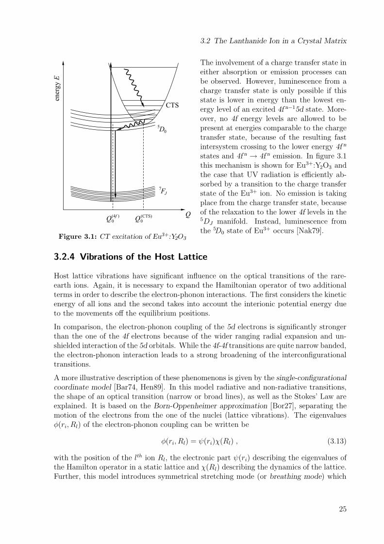
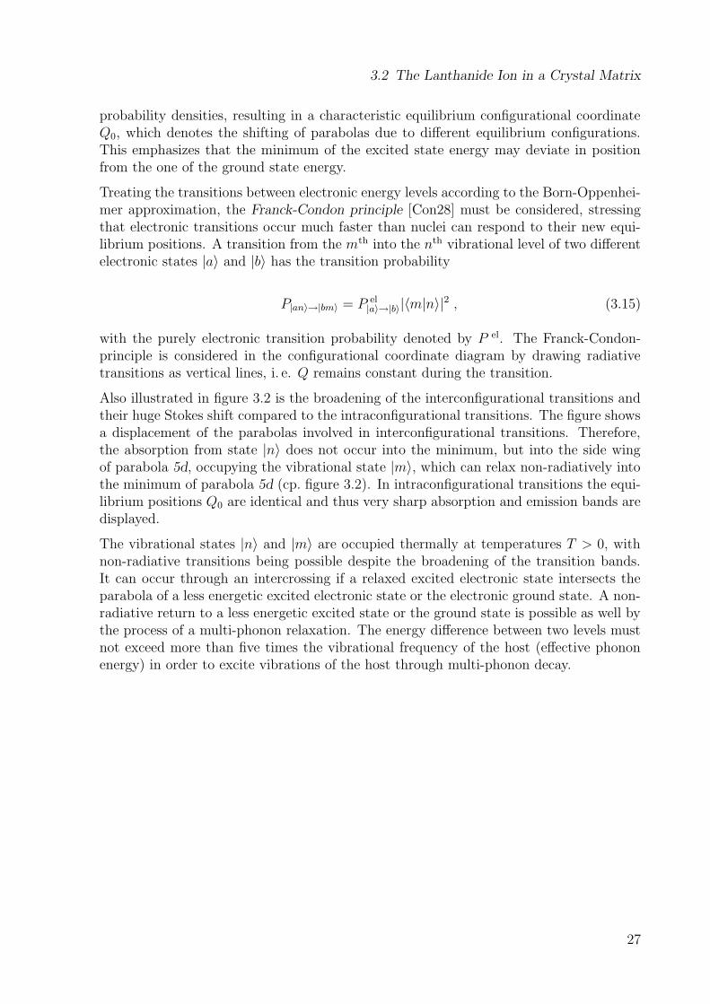
Illustrated in the corresponding configurational coordinate diagram (cp. figure 3.2) arethe potential energy curves of a 4f ground state, a 4f excited state, and a 5d excitedstate of a localized lanthanide ion as a function of the configurational coordinate Q. Thiscoordinate describes the average distance between the central ion and the ligands.
The vibrational motion being of harmonic nature is displayed in the diagram by paraboliccurves with the well-known quadratic dependence of the potential energy Vpot on Q
Vpot =12k (Q−Q0)
2 . (3.14)
The restoring force constant of the vibrational motion is represented by the factor k.The horizontal lines in the diagram refer to the discrete, vibrational levels of energyEm = (m+ 1
2)~ωm which are yielded by the quantum mechanical solution of this equation.
The strength of the electron-phonon coupling is symbolized by the slope of the parabola.Parabola with wider aperture have smaller electron-phonon coupling and vice versa. Thiseffect is shown for the 4f and 5d states in a lanthanide ion in the aforementioned figure 3.2.More influenced by lattice vibrations are the 5d states, with their restoring forces beingtherefore larger than those of the 4f states, i. e. k(5d) > k(4f ).
Each active ion configuration has a certain spatial dimension because of different radial
E
(4f)0Q (5d)
0QQ
(5d)0E
(4f')0E
(4f)0E
n
n
Eph
(5d)potV
(4f ')potV
(4f)potV
y c4f ' 4f '
y c4f 4f
y c5d 5d stokesshift
absorption emission
0
m
Figure 3.2: Configurational coordinate diagram of the 4f and 5d states in alanthanide ion
26
3.2 The Lanthanide Ion in a Crystal Matrix
probability densities, resulting in a characteristic equilibrium configurational coordinateQ0, which denotes the shifting of parabolas due to different equilibrium configurations.This emphasizes that the minimum of the excited state energy may deviate in positionfrom the one of the ground state energy.
Treating the transitions between electronic energy levels according to the Born-Oppenhei-mer approximation, the Franck-Condon principle [Con28] must be considered, stressingthat electronic transitions occur much faster than nuclei can respond to their new equi-librium positions. A transition from the mth into the nth vibrational level of two differentelectronic states |a〉 and |b〉 has the transition probability
P|an〉→|bm〉 = P el|a〉→|b〉|〈m|n〉|2 , (3.15)
with the purely electronic transition probability denoted by P el. The Franck-Condon-principle is considered in the configurational coordinate diagram by drawing radiativetransitions as vertical lines, i. e. Q remains constant during the transition.
Also illustrated in figure 3.2 is the broadening of the interconfigurational transitions andtheir huge Stokes shift compared to the intraconfigurational transitions. The figure showsa displacement of the parabolas involved in interconfigurational transitions. Therefore,the absorption from state |n〉 does not occur into the minimum, but into the side wingof parabola 5d, occupying the vibrational state |m〉, which can relax non-radiatively intothe minimum of parabola 5d (cp. figure 3.2). In intraconfigurational transitions the equi-librium positions Q0 are identical and thus very sharp absorption and emission bands aredisplayed.
The vibrational states |n〉 and |m〉 are occupied thermally at temperatures T > 0, withnon-radiative transitions being possible despite the broadening of the transition bands.It can occur through an intercrossing if a relaxed excited electronic state intersects theparabola of a less energetic excited electronic state or the electronic ground state. A non-radiative return to a less energetic excited state or the ground state is possible as well bythe process of a multi-phonon relaxation. The energy difference between two levels mustnot exceed more than five times the vibrational frequency of the host (effective phononenergy) in order to excite vibrations of the host through multi-phonon decay.
27
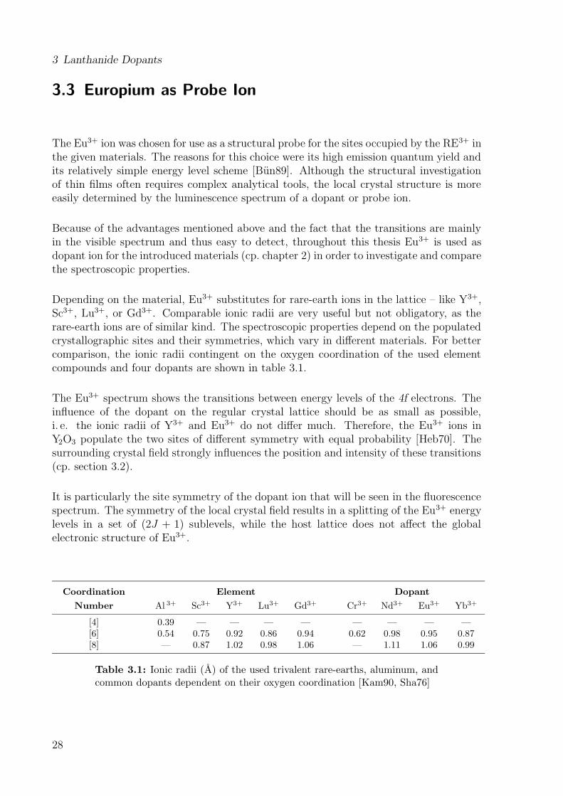
3 Lanthanide Dopants
3.3 Europium as Probe Ion
The Eu3+ ion was chosen for use as a structural probe for the sites occupied by the RE3+ inthe given materials. The reasons for this choice were its high emission quantum yield andits relatively simple energy level scheme [Bun89]. Although the structural investigationof thin films often requires complex analytical tools, the local crystal structure is moreeasily determined by the luminescence spectrum of a dopant or probe ion.
Because of the advantages mentioned above and the fact that the transitions are mainlyin the visible spectrum and thus easy to detect, throughout this thesis Eu3+ is used asdopant ion for the introduced materials (cp. chapter 2) in order to investigate and comparethe spectroscopic properties.
Depending on the material, Eu3+ substitutes for rare-earth ions in the lattice – like Y3+,Sc3+, Lu3+, or Gd3+. Comparable ionic radii are very useful but not obligatory, as therare-earth ions are of similar kind. The spectroscopic properties depend on the populatedcrystallographic sites and their symmetries, which vary in different materials. For bettercomparison, the ionic radii contingent on the oxygen coordination of the used elementcompounds and four dopants are shown in table 3.1.
The Eu3+ spectrum shows the transitions between energy levels of the 4f electrons. Theinfluence of the dopant on the regular crystal lattice should be as small as possible,i. e. the ionic radii of Y3+ and Eu3+ do not differ much. Therefore, the Eu3+ ions inY2O3 populate the two sites of different symmetry with equal probability [Heb70]. Thesurrounding crystal field strongly influences the position and intensity of these transitions(cp. section 3.2).
It is particularly the site symmetry of the dopant ion that will be seen in the fluorescencespectrum. The symmetry of the local crystal field results in a splitting of the Eu3+ energylevels in a set of (2J + 1) sublevels, while the host lattice does not affect the globalelectronic structure of Eu3+.
Coordination Element Dopant
Number Al 3+ Sc3+ Y3+ Lu3+ Gd3+ Cr3+ Nd3+ Eu3+ Yb3+
[4] 0.39 — — — — — — — —[6] 0.54 0.75 0.92 0.86 0.94 0.62 0.98 0.95 0.87[8] — 0.87 1.02 0.98 1.06 — 1.11 1.06 0.99
Table 3.1: Ionic radii (A) of the used trivalent rare-earths, aluminum, andcommon dopants dependent on their oxygen coordination [Kam90, Sha76]
28
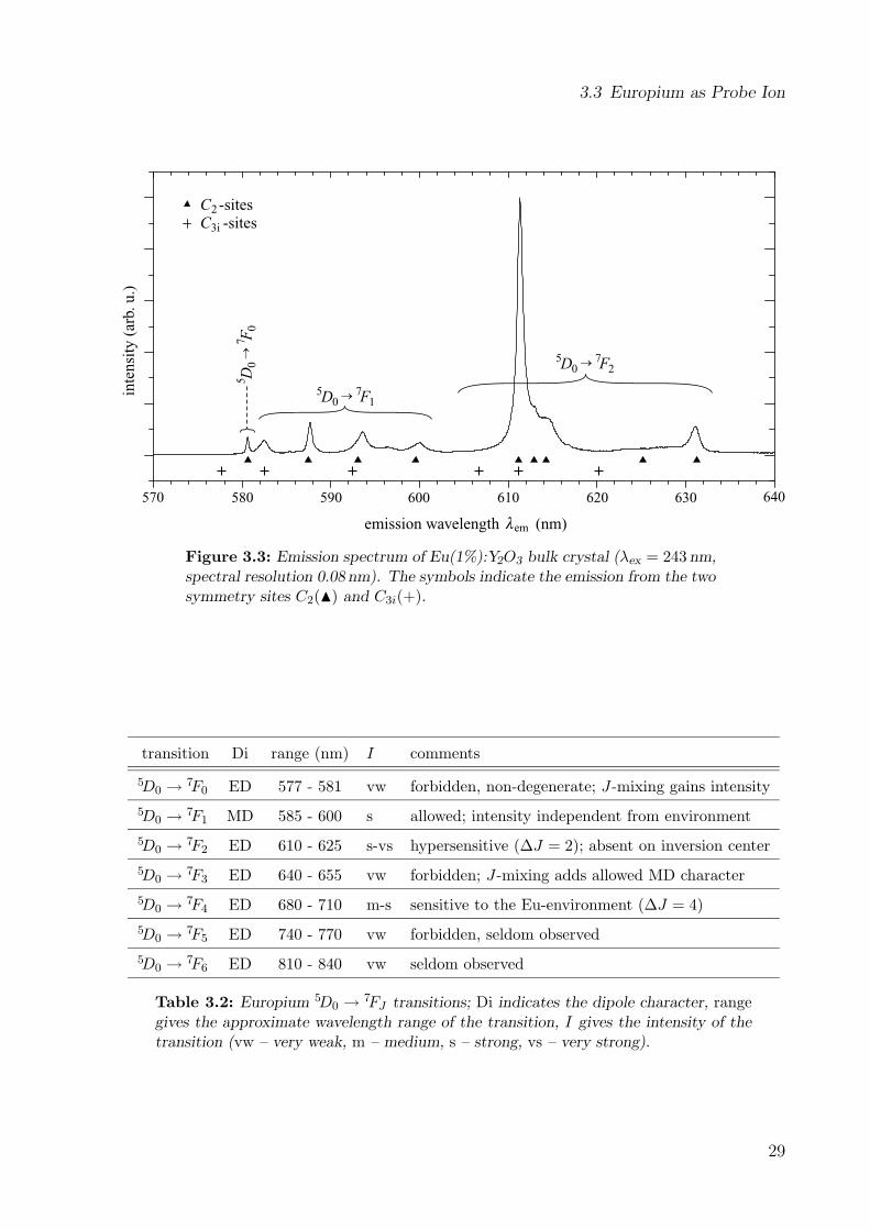
3.3 Europium as Probe Ion
570 580 590 600 610 620 630 640
emission wavelength (nm)lem
inte
nsity
(ar
b. u
.)
C -sitesC -sites
2
3i
®5D0
7F2
®5 D
07 F
0
®5D0
7F1
Figure 3.3: Emission spectrum of Eu(1%):Y2O3 bulk crystal (λex = 243 nm,spectral resolution 0.08 nm). The symbols indicate the emission from the twosymmetry sites C2(N) and C3i(+).
transition Di range (nm) I comments
5D0 → 7F0 ED 577 - 581 vw forbidden, non-degenerate; J-mixing gains intensity
5D0 → 7F1 MD 585 - 600 s allowed; intensity independent from environment
5D0 → 7F2 ED 610 - 625 s-vs hypersensitive (∆J = 2); absent on inversion center
5D0 → 7F3 ED 640 - 655 vw forbidden; J-mixing adds allowed MD character
5D0 → 7F4 ED 680 - 710 m-s sensitive to the Eu-environment (∆J = 4)
5D0 → 7F5 ED 740 - 770 vw forbidden, seldom observed
5D0 → 7F6 ED 810 - 840 vw seldom observed
Table 3.2: Europium 5D0 → 7FJ transitions; Di indicates the dipole character, rangegives the approximate wavelength range of the transition, I gives the intensity of thetransition (vw – very weak, m – medium, s – strong, vs – very strong).
29
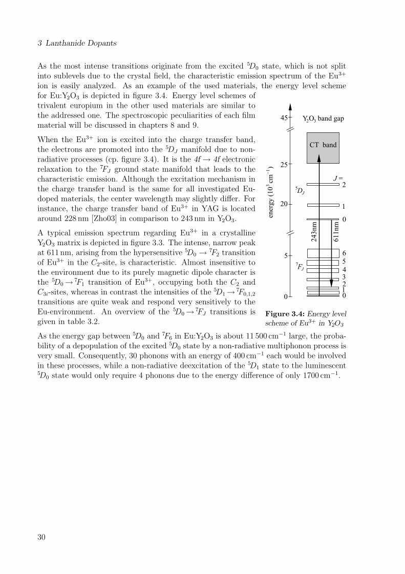
3 Lanthanide Dopants
As the most intense transitions originate from the excited 5D0 state, which is not splitinto sublevels due to the crystal field, the characteristic emission spectrum of the Eu3+
ion is easily analyzed. As an example of the used materials, the energy level scheme
DJ5
FJ7
5
20
25
45
J =2
1
0
65
O band gapY2 3
611n
m
243n
m
432
010
ener
gy (
10 c
m
)1
3_
CT band
Figure 3.4: Energy levelscheme of Eu3+ in Y2O3
for Eu:Y2O3 is depicted in figure 3.4. Energy level schemes oftrivalent europium in the other used materials are similar tothe addressed one. The spectroscopic peculiarities of each filmmaterial will be discussed in chapters 8 and 9.
When the Eu3+ ion is excited into the charge transfer band,the electrons are promoted into the 5DJ manifold due to non-radiative processes (cp. figure 3.4). It is the 4f → 4f electronicrelaxation to the 7FJ ground state manifold that leads to thecharacteristic emission. Although the excitation mechanism inthe charge transfer band is the same for all investigated Eu-doped materials, the center wavelength may slightly differ. Forinstance, the charge transfer band of Eu3+ in YAG is locatedaround 228 nm [Zho03] in comparison to 243 nm in Y2O3.
A typical emission spectrum regarding Eu3+ in a crystallineY2O3 matrix is depicted in figure 3.3. The intense, narrow peakat 611 nm, arising from the hypersensitive 5D0 → 7F2 transitionof Eu3+ in the C2-site, is characteristic. Almost insensitive tothe environment due to its purely magnetic dipole character isthe 5D0→ 7F1 transition of Eu3+, occupying both the C2 andC3i-sites, whereas in contrast the intensities of the 5D1→ 7F0,1,2transitions are quite weak and respond very sensitively to theEu-environment. An overview of the 5D0→ 7FJ transitions isgiven in table 3.2.
As the energy gap between 5D0 and7F6 in Eu:Y2O3 is about 11 500 cm
−1 large, the proba-bility of a depopulation of the excited 5D0 state by a non-radiative multiphonon process isvery small. Consequently, 30 phonons with an energy of 400 cm−1 each would be involvedin these processes, while a non-radiative deexcitation of the 5D1 state to the luminescent5D0 state would only require 4 phonons due to the energy difference of only 1700 cm−1.
30
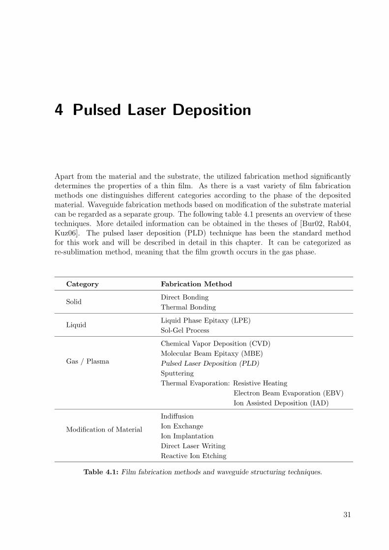
4 Pulsed Laser Deposition
Apart from the material and the substrate, the utilized fabrication method significantlydetermines the properties of a thin film. As there is a vast variety of film fabricationmethods one distinguishes different categories according to the phase of the depositedmaterial. Waveguide fabrication methods based on modification of the substrate materialcan be regarded as a separate group. The following table 4.1 presents an overview of thesetechniques. More detailed information can be obtained in the theses of [Bur02, Rab04,Kuz06]. The pulsed laser deposition (PLD) technique has been the standard methodfor this work and will be described in detail in this chapter. It can be categorized asre-sublimation method, meaning that the film growth occurs in the gas phase.
Category Fabrication Method
SolidDirect Bonding
Thermal Bonding
LiquidLiquid Phase Epitaxy (LPE)
Sol-Gel Process
Gas / Plasma
Chemical Vapor Deposition (CVD)
Molecular Beam Epitaxy (MBE)
Pulsed Laser Deposition (PLD)
Sputtering
Thermal Evaporation: Resistive Heating
Electron Beam Evaporation (EBV)
Ion Assisted Deposition (IAD)
Modification of Material
Indiffusion
Ion Exchange
Ion Implantation
Direct Laser Writing
Reactive Ion Etching
Table 4.1: Film fabrication methods and waveguide structuring techniques.
31
4 Pulsed Laser Deposition
The history of pulsed laser deposition (PLD) began in 1965 when Smith and Turnerdemonstrated the deposition of thin films by ablating material with a pulsed ruby laser[Smi65]. Not long before, in 1962, Breech and Cross had shown that material could beablated by laser radiation [Bre62] – laying the foundation for the development soon tocome in 1965. In the first PLD experiment, Smith and Turner were able to produce‘optically satisfactory’ films of different sorts, like Sb2S3, ZnTe, and PbCl2.
However, it was not before 1987 that stronger attention was drawn to PLD when Dijkampet al. applied this technique to fabricate thin films of YBa2Cu3O4−δ (YBCO), which wasat that time considered a promising new high-temperature superconductor [Dij87]. Thenewly risen attraction was due to the successful demonstration of depositing a complexmaterial like YBCO and because the degree of stoichiometric control in PLD was superiorto the one achieved by evaporation or sputtering techniques. Today, pulsed laser deposi-tion is not only employed to produce crystalline films of epitaxial quality but also to createnanostructures at atomic scale, combining for instance conductor and isolator materials.Also strong efforts are made to achieve improving waveguide materials by PLD.
The principle of PLD is quite simple as the technique is based on physical processes thatarise from the impact of high-power pulsed laser radiation on solid targets, leading to theremoval of partially ionized material from the impact zone (plasma). In short, the pulsedlaser beam is focused on solid target material that is evaporated due to the depositedenergy. The evaporated material expands from the target surface and is deposited ona substrate which is placed on the opposite side (cp. figure 4.1). Vacuum condition orreduced ambient atmosphere is required for the ablation process, since the ablated materialcan not reach the substrate under atmospheric pressure. The PLD process takes placefar away from equilibrium and involves a large number of complex physical and chemicalmechanisms with lots of variables. It should be emphasized that, in spite of the simplicityof the general idea and its realization, the processes taking place during ablation anddeposition are complex and not fully understood up to now. Most of the research in thisarea is empirical due to the fact that analytical descriptions of the processes involved areextremely difficult.
A brief introduction to these mechanisms is given in this section, also referring to a varietyof published articles and books analyzing this technique in more detail, e. g. [Bau00,Chr94]. Two review articles dealing with the processes of pulsed laser deposition by K. L.Saenger are worth noticing [Sae93a, Sae93b]. Therein, a precise overview of the historyof PLD is given as well as the physical mechanisms.
The deposition process can be subdivided into four stages:
1. Interaction of laser radiation with the target leading to ablation;2. Spatial expansion of the ablation products (plasma) –
including interaction and chemical reaction within the plasma;3. Interaction of the ablation products with the substrate;4. Nucleation and growth of thin film on the substrate surface.
A simplified scheme of these four stages is shown in figure 4.1. The different processes willbe described in the following sections, as the properties like crystallinity, stoichiometry,and surface roughness of the obtained films are influenced by each stage.
32
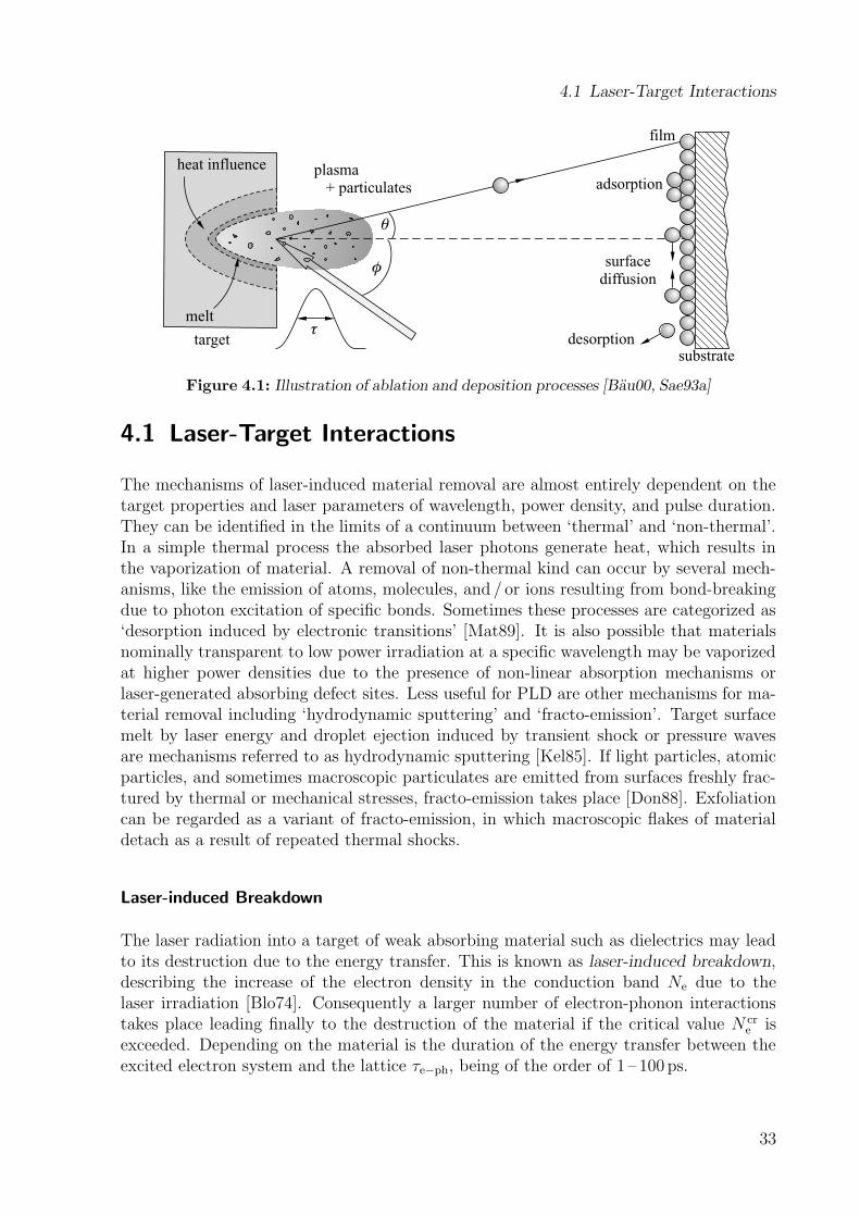
4.1 Laser-Target Interactions
q
f
ttarget
substrate
film
adsorption
desorption
surfacediffusion
melt
heat influence plasma+ particulates
Figure 4.1: Illustration of ablation and deposition processes [Bau00, Sae93a]
4.1 Laser-Target Interactions
The mechanisms of laser-induced material removal are almost entirely dependent on thetarget properties and laser parameters of wavelength, power density, and pulse duration.They can be identified in the limits of a continuum between ‘thermal’ and ‘non-thermal’.In a simple thermal process the absorbed laser photons generate heat, which results inthe vaporization of material. A removal of non-thermal kind can occur by several mech-anisms, like the emission of atoms, molecules, and / or ions resulting from bond-breakingdue to photon excitation of specific bonds. Sometimes these processes are categorized as‘desorption induced by electronic transitions’ [Mat89]. It is also possible that materialsnominally transparent to low power irradiation at a specific wavelength may be vaporizedat higher power densities due to the presence of non-linear absorption mechanisms orlaser-generated absorbing defect sites. Less useful for PLD are other mechanisms for ma-terial removal including ‘hydrodynamic sputtering’ and ‘fracto-emission’. Target surfacemelt by laser energy and droplet ejection induced by transient shock or pressure wavesare mechanisms referred to as hydrodynamic sputtering [Kel85]. If light particles, atomicparticles, and sometimes macroscopic particulates are emitted from surfaces freshly frac-tured by thermal or mechanical stresses, fracto-emission takes place [Don88]. Exfoliationcan be regarded as a variant of fracto-emission, in which macroscopic flakes of materialdetach as a result of repeated thermal shocks.
Laser-induced Breakdown
The laser radiation into a target of weak absorbing material such as dielectrics may leadto its destruction due to the energy transfer. This is known as laser-induced breakdown,describing the increase of the electron density in the conduction band Ne due to thelaser irradiation [Blo74]. Consequently a larger number of electron-phonon interactionstakes place leading finally to the destruction of the material if the critical value N cr
e isexceeded. Depending on the material is the duration of the energy transfer between theexcited electron system and the lattice τe−ph, being of the order of 1 – 100 ps.
33
4 Pulsed Laser Deposition
The above described effect is based on ‘free’ electrons in the conduction band. Theseare present only in small numbers of 108 – 1010 cm−3 in dielectrics [Blo74] and can be ob-tained in two ways when using high radiation intensities in the range of 1011 – 1014W/cm2:
1. By non-linear multi-phonon absorption leading to ionization (MPA),
2. By absorption of the laser radiation by present electrons in the conductionband (free-carrier-absorption) and subsequent avalanche ionization (AI).
In the latter case, the large electric field of the radiation accelerates the free electrons inthe conduction band. The surrounding atoms are ionized by these high-energy electronscreating new free electrons that are also accelerated. The result is an avalanche-likeproduction of electrons.
The following rate equation describes the time dependence of the electron density Ne inthe conduction band in the near-surface region during the presence of a laser pulse withintensity I(t) [Stu96]
dNe
dt= εav I(t)Ne(t)︸ ︷︷ ︸
AI
+ γm Im(t)
︸ ︷︷ ︸
MPA
, (4.1)
with εav denoting the avalanche coefficient, γm being the multi-phonon absorption coef-ficient for the absorption of m photons, and m being the minimum number of photonsfor a transition between valence band and conduction band. An important experimen-tal parameter is the threshold intensity Ithr for which the critical electron density N cr
e isreached. Because the laser fluence Φ is defined as the total energy per unit area per pulse
Φ =
∫ τ
0
I(t) dt , (4.2)
it is obvious with regard to equation 4.1 that the threshold fluence is independent of thepulse duration τ , thus having a constant value if only considering the avalanche ionization;
Φthr(τ) =1
εavln
(N cre
N0
)
. (4.3)
Though assuming a square-wave pulse, in the case of purem-photon absorption the thresh-old fluence scales with τ
m−1m . This underlines the importance and the gain of an experi-
mental determination of Φthr in order to obtain a more detailed insight into the physicalmechanisms leading to damage in dielectrics.
In case of long pulse durations with a laser-target interaction being in the range of nano-second pulses, the heating of the lattice during the pulse has to be considered (τ À τe−ph).Changed plasma properties are the result because of the expanding plasma interactingwith the incoming laser beam (shielding effect) and this leading to a reduced energytransfer into the target.
Under the premise of nanosecond pulses with τ À τe−ph being valid, the material removalcaused by heat will be briefly investigated in the following.
34
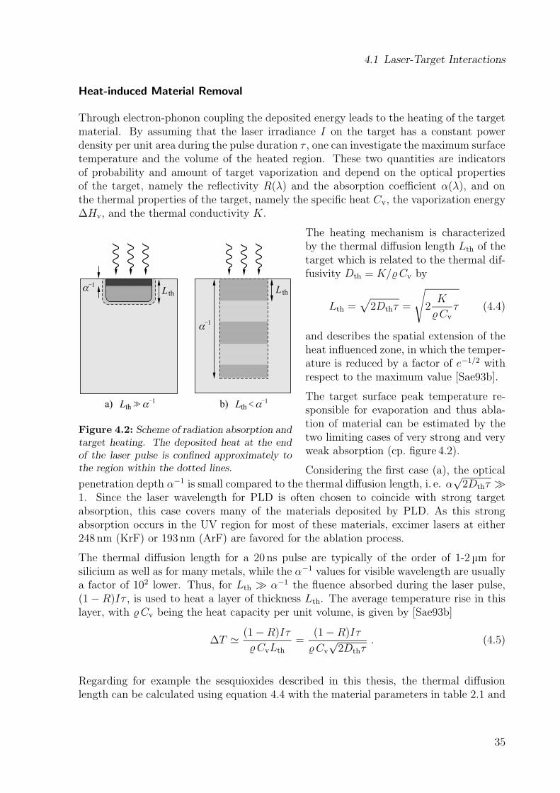
4.1 Laser-Target Interactions
Heat-induced Material Removal
Through electron-phonon coupling the deposited energy leads to the heating of the targetmaterial. By assuming that the laser irradiance I on the target has a constant powerdensity per unit area during the pulse duration τ , one can investigate the maximum surfacetemperature and the volume of the heated region. These two quantities are indicatorsof probability and amount of target vaporization and depend on the optical propertiesof the target, namely the reflectivity R(λ) and the absorption coefficient α(λ), and onthe thermal properties of the target, namely the specific heat Cv, the vaporization energy∆Hv, and the thermal conductivity K.
L th L tha
a
1_
1_
L a>>th1
_
a) 1_
L a>thb)
Figure 4.2: Scheme of radiation absorption andtarget heating. The deposited heat at the endof the laser pulse is confined approximately tothe region within the dotted lines.
The heating mechanism is characterizedby the thermal diffusion length Lth of thetarget which is related to the thermal dif-fusivity Dth = K/%Cv by
Lth =√
2Dthτ =
√
2K
%Cv
τ (4.4)
and describes the spatial extension of theheat influenced zone, in which the temper-ature is reduced by a factor of e−1/2 withrespect to the maximum value [Sae93b].
The target surface peak temperature re-sponsible for evaporation and thus abla-tion of material can be estimated by thetwo limiting cases of very strong and veryweak absorption (cp. figure 4.2).
Considering the first case (a), the opticalpenetration depth α−1 is small compared to the thermal diffusion length, i. e. α
√2Dthτ À
1. Since the laser wavelength for PLD is often chosen to coincide with strong targetabsorption, this case covers many of the materials deposited by PLD. As this strongabsorption occurs in the UV region for most of these materials, excimer lasers at either248 nm (KrF) or 193 nm (ArF) are favored for the ablation process.
The thermal diffusion length for a 20 ns pulse are typically of the order of 1-2 � m forsilicium as well as for many metals, while the α−1 values for visible wavelength are usuallya factor of 102 lower. Thus, for Lth À α−1 the fluence absorbed during the laser pulse,(1− R)Iτ , is used to heat a layer of thickness Lth. The average temperature rise in thislayer, with %Cv being the heat capacity per unit volume, is given by [Sae93b]
∆T ' (1−R)Iτ%CvLth
=(1−R)Iτ%Cv
√2Dthτ
. (4.5)
Regarding for example the sesquioxides described in this thesis, the thermal diffusionlength can be calculated using equation 4.4 with the material parameters in table 2.1 and
35
4 Pulsed Laser Deposition
a pulse duration of τ = 15 ns. As no values are available for Cv, Cp is used instead andsince Cp ≤ Cv
1, the lower limit of Lth is determined to be
Lth =
√
2Kτ
%Cv
>
√
2Kτ
%Cp
≈ 30 � m .
The optical absorption depth α−1 for the KrF-laser can be estimated by an absorptionspectrum (α−1 ¿ 10 � m) [Mix99], whereas the values of n and k are calculated by [Pal85].The relation between α and k is [Bor75]
α =4πk
λ, (4.6)
resulting in α−1 ≈ 46 nm at λ = 248 nm and k = 0.427.
The optical absorption length α−1 in the other case (b) is larger than the thermal diffusionlength, i. e. α
√2Dthτ < 1. An exponential temperature profile along the depth z is created
by the absorption of radiation that corresponds to the absorption profile, i. e. [Sae93b]
∆T (z) =(1−R)α I e−αzτ
%Cv
. (4.7)
As described by this equation, the heat is rapidly transported away from the ablation area.This leads to melting and, in some cases, to the evaporation of the target material, bothpreventing the desired congruent evaporation. At very high fluences even the superheatingof a large volume due to large absorption depths is possible. This heating results in moltendroplets or particulates as the heated volume will be transformed into the melting phaseand ejected from the surface due to rapid expansion.
However, in both cases (a) and (b) macroscopic material removal by vaporization is ex-pected if the heat absorbed per unit volume exceeds the energy density corresponding tothe latent heat of vaporization, %∆Hv. In the first case (a) the condition yields that athreshold fluence of
Φthr >%∆Hv Lth
(1−R) (4.8)
has to be reached before material vaporization to a depth Lth is initiated. Though, theexperimentally observed threshold values might be lower than the calculated ones, due tothe non-perfect target morphology. Non-homogeneous evaporation mechanisms (ablationof clusters or particles, multiple pulse effects) also affects the threshold fluence and isresponsible for differing experimentally observed values Φthr.
As a direct consequence of one-dimensional heat flow for pulse durations > τe−ph, theequations 4.4 and 4.8 show that the threshold fluence Φthr defined in equation 4.2 isproportional to
√τ for vaporization. It becomes obvious in this relation that in using
very short pulse-lasers with pico- or femtosecond pulses instead of nanosecond pulseseither the same material vaporization should be possible at lower laser fluences or higher
1 Cv equals Cp solely for T = 0
36
4.1 Laser-Target Interactions
vaporization rates should be accessed for identical fluence. Nevertheless an implication offs-lasers being more suitable for the ablation of material would be wrong because, as it isshown in the following, the interaction of the laser pulse with the developing plasma canalso have beneficial effects on the plume species.
Influence of Target Morphology
The material removal is affected by the target surface and its morphology in various ways.The expanding vapor plume has a preferred direction being perpendicular to the targetsurface, as section 4.2 will show in detail. A rough surface will cause the direction ofthe plume to change during the ablation process, resulting in non-uniform films on thesubstrate. Another problematic occurrence is the change of the target morphology afterirradiation with many laser pulses due to recrystallization or development of macroscopicfeatures such as craters. A bending of the plasma plume towards the incident laser beamis caused by structures like this, which again will lead to non-uniform material deposition[Bau00].
Thermal properties are additionally influencing the ablation process. Though being of thesame material, the thermal diffusion length may vary regarding a sintered target versusa single-crystal. Bulk materials as single-crystals or amorphous materials are usuallyapplied as targets in order to reduce the generation of particulates. Nevertheless, if thecorresponding bulk material is transparent to the laser length, a compressed and sinteredpowder target may be preferred. The absorption of the target will then be enhanced byscattering effects [San85].
Stoichiometry of Removed Material
In pulsed laser deposition the material flux from the target usually matches the targetstoichiometry. This ‘congruent’ vaporization, pertinent to targets which incorporate mul-tiple components like Eu:(Gd, Lu)3AL5O12, is a very important benefit of the pulsed laserdeposition technique. It is explained by the pulsed laser heating, which is a highly non-equilibrium process. A very high heating rate (108K/s) of the surface is caused by thepulsed ns-laser irradiation due to the large optical absorption coefficient and, in the caseof sintered material, due to the poor thermal conductivity [Bec88]. Thus, qualitatively ex-plaining, material removal occurs before the individual components of the target materialcan segregate into low and high vapor pressure components [Che88].
Particulate Generation
The deposition of particulates which are produced together with the vapor during theablation process is one of the major drawbacks of PLD. These particulates, rangingfrom several hundred nanometers to a few tens of micrometers in size, are responsiblefor poor film quality because of their adverse effect on the growth of the subsequent
37
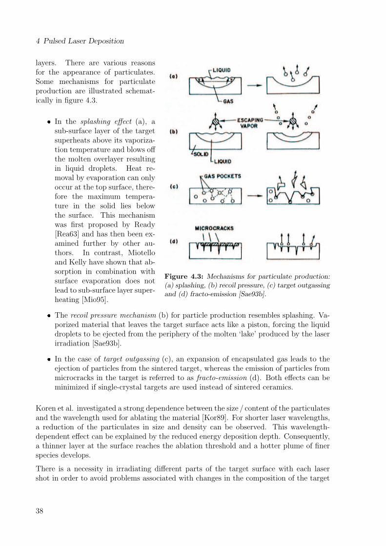
4 Pulsed Laser Deposition
Figure 4.3: Mechanisms for particulate production:(a) splashing, (b) recoil pressure, (c) target outgassingand (d) fracto-emission [Sae93b].
layers. There are various reasonsfor the appearance of particulates.Some mechanisms for particulateproduction are illustrated schemat-ically in figure 4.3.
� In the splashing effect (a), asub-surface layer of the targetsuperheats above its vaporiza-tion temperature and blows offthe molten overlayer resultingin liquid droplets. Heat re-moval by evaporation can onlyoccur at the top surface, there-fore the maximum tempera-ture in the solid lies belowthe surface. This mechanismwas first proposed by Ready[Rea63] and has then been ex-amined further by other au-thors. In contrast, Miotelloand Kelly have shown that ab-sorption in combination withsurface evaporation does notlead to sub-surface layer super-heating [Mio95].
� The recoil pressure mechanism (b) for particle production resembles splashing. Va-porized material that leaves the target surface acts like a piston, forcing the liquiddroplets to be ejected from the periphery of the molten ‘lake’ produced by the laserirradiation [Sae93b].
� In the case of target outgassing (c), an expansion of encapsulated gas leads to theejection of particles from the sintered target, whereas the emission of particles frommicrocracks in the target is referred to as fracto-emission (d). Both effects can beminimized if single-crystal targets are used instead of sintered ceramics.
Koren et al. investigated a strong dependence between the size / content of the particulatesand the wavelength used for ablating the material [Kor89]. For shorter laser wavelengths,a reduction of the particulates in size and density can be observed. This wavelength-dependent effect can be explained by the reduced energy deposition depth. Consequently,a thinner layer at the surface reaches the ablation threshold and a hotter plume of finerspecies develops.
There is a necessity in irradiating different parts of the target surface with each lasershot in order to avoid problems associated with changes in the composition of the target
38
4.2 The Plasma Plume
surface [Auc88, Coh91] or with crater formation in the target, which results in a skewedplume direction and a higher concentration of particulates [Bec88]. Different techniqueshave been developed to achieve this, like rotating the target while keeping the laser spot ina fixed position slightly displaced from the rotation axis resulting in ring-shaped ablationtracks. Another option can be found in scanning the laser beam over the target surfaceby using mirrors to control this laser scan while keeping the target in a fixed position.
As this brief overview made clear, there is a variety of processes involved in particulategeneration. This implies even more complexity due to the fact that these processes may beoperative at the same time [Ugl77]. Thus, no ‘simple’ correlation between film particulatecontent and target thermal properties could be found [Dup89]. However, a good possibilityto eliminate particulates is given by a high-speed velocity filter due to the velocities ofparticulates being one order of magnitude smaller than those of atoms and ions [Dup89,Bar69].
4.2 The Plasma Plume
The previous section described the absorption of the incident laser radiation by the targetleading to the evaporation of material. Initially, this hot and dense vapor is confined toa very small volume near the target surface that may contain many species as atoms,molecules, ions, free electrons, and in some cases also large particulates. Once the contentof charged particles in this vapor exceeds a critical value, it is called plasma, being ofquasi-neutral manner in general with as many positive charges as negative ones.
Applying the Boltzmann distribution in order to derive the degree of ionization in thermalequilibrium, i. e. the ratio of the density of ions ni and the density of neutral atoms n0,the Eggert–Saha equation can be obtained [Egg19, Sah21]
ni nen0
= 2gig0
(2πmekT
h2
)3/2
e−Wi/kBT . (4.9)
In this equation ne denotes the electron number density, me the electron mass, kB is theBoltzmann constant, h is Planck’s constant, and gi as well as g0 are the statistical weightsfor the electron-ion pair and the neutral atom, respectively. Wi is the ionization potential,i. e. the energy necessary to remove an electron from an atom.
The equation 4.9 of Eggert–Saha is derived on the premise of isolated and non-interactingatoms. Thus, its applicability does not include high plasma densities, in which the effectiveionization energy is lowered by the overlap of the neighboring ion potentials. Consequentlythe degree of ionization is higher than predicted by equation 4.9. Another limitation of theEggert–Saha equation is the counter case of having low densities, in which the conditionof a thermodynamic equilibrium may not be fulfilled.
Although there is no thermodynamic transition defined between the gas phase and theplasma phase in general, equation 4.9 reveals that at temperatures of several 1000K thedegree of ionization increases from nearly 0 to 1. Assuming typical values of Wi ≈ 10 eV
39
4 Pulsed Laser Deposition
and T ≈ 10 000K, the plasma is initially characterized by neutral particle densities of1019 − 1020 cm−3 and electron densities of 1017 − 1020 cm−3 [Sae93b].
Laser-Plume Interactions
The interaction between the expanding plasma and the incoming radiation has to beconsidered at laser pulse durations of the order of nanoseconds. This may have negativeas well as positive effects on the film growth process.
It has already been mentioned in section 4.1 that the fraction of laser fluence reachingthe target can be attenuated by these laser-plume interactions. This should be takeninto consideration when using laser fluences high above the threshold fluence, whereasat fluences near the threshold value the plasma plume size is very small and the plasmalocalizes at the substrate surface. An increasing of the fluence leads to a larger ablationvolume and consequently results in an enlarged and denser plume, which interacts stronglywith the incident laser radiation before reaching the target. If sub-picosecond pulses areused, these interactions are ignorable due to plasma velocities of . 106 cm/s [Bau00].
Nevertheless, it is also possible that these interactions have a positive influence on thedeposition process in modifying the composition of the plume species. As the dissociation,ionization and/or electronic excitation of the atoms and molecules in the plume is possibledue to the absorption of one or more laser photons, the relative amount of ions increaseswith respect to neutral molecules and atoms. Free electrons in the plume can also beheated by the inverse bremsstrahlung 2 in which the absorption of a laser photon increasesthe electrons’ kinetic energy in a collision process.
Plasma Expansion
Investigating the plasma expansion, its general dynamic behavior is comparable withthe dynamics of a free-jet adiabatic expansion [Kel92, Zhe89]. A highly forward-peakedmaterial flux and an average particle speed many times higher than the mean randomthermal speed characterize both expansions. It is the kinetic energy of the arriving plumespecies that is regarded as one of the key parameters of film growth on the substrate. Inthermodynamic gas theory this can be described by temperature. The local temperature
2 The term ‘bremsstrahlung’ refers to emitted radiation by charged particles under decelerations whenpassing through the field of atomic nuclei. With m denoting the rest mass of the particle, the energyemitted by an accelerated particle is proportional to 1/m2, which is the reason why bremsstrahlungplays an influential role for light particles such as electrons. Thus, scattering of two electrons resultsin emission of radiation (1) and the inverse process termed ‘inverse bremsstrahlung’ can occur usingintense radiation (2)
e− + e− → e− + e− −∆Ekin + hν (1)
hν + e− + e− → e− + e− +∆Ekin (2) .
In the latter case, a photon is absorbed and the kinetic energy of the electrons is increased corre-spondingly.
40
4.2 The Plasma Plume
T (z) and density n(z) are related to
T (z)
T0=
[n(z)
n0
]γ−1
, (4.10)
when assuming the adiabatic expansion of a high-pressure gas and the one-dimensionalcharacter of the expansion. Therein, T0 and n0 are the initial temperature and density,and γ = CV/Cp is the ratio of constant volume and constant pressure specific heats. Itis estimated that in laser-produced plasmas with temperatures up to 105K γ is about1.2 - 1.3 [Sin90, Sae93b]. A fall-off regarding the temperature as well as the density ofthe plume can be observed during the spatial plasma expansion, the latter as the inversecube of the distance from the target, i. e. n(z)/n0 ∝ d−3, in a simplified spherical model[Sin90].
Thus, the collision rate of the plume species decreases and the random kinetic energy ofthe particles is converted to a directed motion away from the target. This behavior is notvalid for effusive sources, e. g. in EBV processes. It can only be applied to supersonicsources, such as laser-produced plasmas.
Effects of the Background Gas
The expansion of the plume is not completely described by the considerations made inthe last section, as the expansion strongly depends on the presence of a backgroundgas often used during the deposition process. Any type of background gas significantlyinfluences the plume transport and its appearance. The scattering of the plume species,for example, reduces the velocity and amount of material reaching the substrate. Anotherexample are chemical reactions that change the initial composition of species, result indifferent optical emission characteristics and finally change the shape of the plume due tophysical confinement.
Reactive oxygen has been used as background gas for all depositions presented in thisthesis. Consequently, when growing a sesquioxide such as Y2O3, the formation of Y∗
and YO∗ takes place with the asterisk indicating electronic excitation [Dye91]. The lat-ter byproduct YO∗ is not an effect of the ablation process, but directly related to theexothermic Y + O2 plasma-background gas reaction. These transformations all have aneffect on the growth mechanism of the substrate–film. Having very low oxygen pressureor even an inert atmosphere during the deposition of oxides like Y2O3, the grown films arein general not matching the correct stoichiometric composition inter alia due to oxygendeficiencies.
After the plume-dynamics have been successfully described by K. L. Sanger using thesimilarity to adiabatic supersonic expansion of gaseous jets and giving an explanationof the plume angular distribution [Sae89], Bulgakov and Bulgakova have developed asimplified model for the plume expansion in an ambient gas [Bul98]. It is based on thetheory of a supersonic jet that is formed when a high-pressure gas streams through anozzle into a low-pressure gas, thus being also termed ‘underexpanded jet’.
41
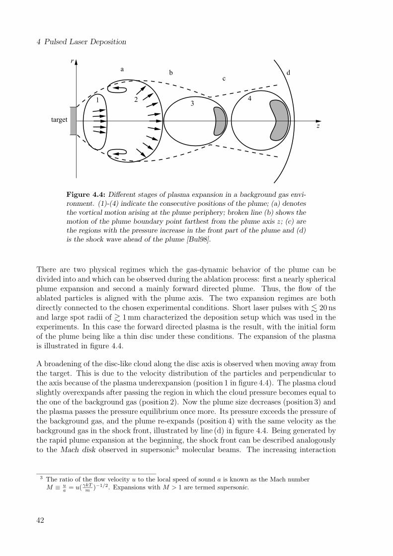
4 Pulsed Laser Deposition
1
ra
target
bc
d
z
2 34
Figure 4.4: Different stages of plasma expansion in a background gas envi-ronment. (1)-(4) indicate the consecutive positions of the plume; (a) denotesthe vortical motion arising at the plume periphery; broken line (b) shows themotion of the plume boundary point farthest from the plume axis z; (c) arethe regions with the pressure increase in the front part of the plume and (d)is the shock wave ahead of the plume [Bul98].
There are two physical regimes which the gas-dynamic behavior of the plume can bedivided into and which can be observed during the ablation process: first a nearly sphericalplume expansion and second a mainly forward directed plume. Thus, the flow of theablated particles is aligned with the plume axis. The two expansion regimes are bothdirectly connected to the chosen experimental conditions. Short laser pulses with . 20 nsand large spot radii of & 1mm characterized the deposition setup which was used in theexperiments. In this case the forward directed plasma is the result, with the initial formof the plume being like a thin disc under these conditions. The expansion of the plasmais illustrated in figure 4.4.
A broadening of the disc-like cloud along the disc axis is observed when moving away fromthe target. This is due to the velocity distribution of the particles and perpendicular tothe axis because of the plasma underexpansion (position 1 in figure 4.4). The plasma cloudslightly overexpands after passing the region in which the cloud pressure becomes equal tothe one of the background gas (position 2). Now the plume size decreases (position 3) andthe plasma passes the pressure equilibrium once more. Its pressure exceeds the pressure ofthe background gas, and the plume re-expands (position 4) with the same velocity as thebackground gas in the shock front, illustrated by line (d) in figure 4.4. Being generated bythe rapid plume expansion at the beginning, the shock front can be described analogouslyto the Mach disk observed in supersonic3 molecular beams. The increasing interaction
3 The ratio of the flow velocity u to the local speed of sound a is known as the Mach numberM ≡ u
a = u(γkTm )−1/2. Expansions with M > 1 are termed supersonic.
42
4.2 The Plasma Plume
with the background gas finally stops the plume expansion with
Rmax ∼(mablE
πρbpb
)1/6
(4.11)
giving the maximum propagation length of the plume from the target Rmax in a back-ground gas of mass density ρb and at pressure pb [Bul95]. In this formula, mabl is theejected mass and E the absorbed laser energy. The deposition will proceed by diffusionresulting in low deposition rates, if the final propagation length of the plume is shorterthan the target-substrate distance.
The regions (c) in figure 4.4 show that the particle flow is decelerated during the expansionprocess by the background gas leading to an increased pressure in the front part of theplume. It can be assumed that at this stage a mixing of the cloud material with theambient gas takes place [Ani83] resulting in the strong red YO∗ chemiluminescence, whichcan be observed in experiments dealing with yttrium compounds [Fri93].
Plume Angular Distribution
Usually, the plume is oriented along the surface normal of the target, as depicted in themodel of the plume expansion in an ambient gas. Since the irradiated surface of a perfectlyplanar, isotropic target has no ‘memory’ of the direction from which the absorbed photonsoriginated, this is also valid for non-normal incident laser radiation. Because real targetsare not perfectly planar in most cases, the plume tilting cannot be avoided in practice.One has to take into account too that the laser beam intensity profile may be asymmetricor non-uniform. A good illustration is a hot spot at the center of the laser beam profile,introducing asymmetries in target irradiance due to the shadowing effects of the denserplasma above the corresponding hot spot on the target [Sae93b].
Different contributions to the plasma distribution with distinct physical origins can berelated besides these experimental deviations of the plume direction. It is possible totreat the source of the evaporation, i. e. the irradiated spot on the target, as a small areaeffusive source. It is defined by the ratio d/h¿ 1 with d representing the diameter of thesource (approximately the laser spot size) and h denoting the target-substrate distance.The emission distribution of such source is described by a cos θ law [Mai83].
As the single cosine fit holds only for the broad structure seen in the plume angulardistribution, the enhanced forward peaking of the plume is commonly approximated bya cosn θ function. Therein, the values for the exponent range between 1 < n ≤ 200. Inapplication, a superposition of a cosine and a cosn function in the following form is usedto fit the angular distribution:
a cos(φ− ε) + b cosn(φ− ε) . (4.12)
It is this two-component structure usually being applied to all species, neutral atoms andions, in the plasma plume though A.Thum-Jager and K.Rohr [Thu99] found out thatthe angular profiles depend on the degree of ionization and that for ions with a charge
43

4 Pulsed Laser Deposition
q ≥ 2 the emission can be well described by a single cosn fit. For species of different massthe shape of the distribution varies, observing a relative enrichment of the lower masselements near θ = 0.
As a possibility the narrow angular distribution of the ejected plume towards the substratemay lead to high deposition rates, preventing extensive chamber contamination. However,this can result in non-uniform film thickness and inhomogeneous stoichiometries over largedeposition areas, which are major drawbacks of pulsed laser deposition.
44
5 Lattice Matched Thin Films
Thin films can show a different behavior in comparison to bulk crystals of the samechemical composition. This would indicate a different inner structure. Film growthon a substrate can be of epitaxial, polycrystalline or amorphous kind. The structuresarising during this process may be homogenous, pillar-like or porous. These structuresdo not absorb light as they measure some tens of nanometers [Flo04]. However, they maystrongly influence the optical properties of the grown film. The mechanical properties andthe long-term stability are also of influence.
The fabrication of epitaxially grown crystalline dielectric oxide films is of great tech-nological interest as these materials may be used as active waveguide devices, compactmicrolasers [Gri04], and as crystalline coatings in a thin-disk laser setup [Kuz06]. For allthese applications high-quality thin films are required. Film quality is mainly determinedby the interface between the substrate and the grown film. Thus, lattice matching in filmgrowth and its requirements will be thoroughly explained in the following sections.
Another objective in film growth is that the refractive index difference of substrate and filmshould be preferably high. Even though a great difference between the refractive indexesis advantageous for waveguide usage [Bur02, Bar04, Kuz06], this usually presupposes theepitaxy of different materials with varying lattice constants and structures. In turn, non-epitaxial growth is induced, including stress in the film and point defects, especially at theinterface between the substrate and the grown film. In the case of perfect lattice matchedfilms no interface defects are expected and thus high-quality crystalline growth can beobtained, which is beneficial for waveguide materials as well as for crystalline coatings.
As it is the aim of this thesis to investigate crystalline film growth using various lat-tice matched systems, this chapter first deals with growth mechanisms and particularlywith epitaxial growth in section 5.1. In section 5.2 different crystal structures are pre-sented with the possibilities of combining them. Thereby, different ways to achieve latticematching are shown. Section 5.3 presents the investigated substrate–film systems.
45
5 Lattice Matched Thin Films
5.1 Growth Mechanisms
The term epitaxy (Greek; epi ‘above’ and taxis ‘in ordered manner’) describes an orderedcrystalline growth on a monocrystalline substrate. Therein, the substrate can be regardedas seed crystal and its lattice structure and orientation are continued by the depositedfilm. Three forms of epitaxial growth are distinguished1 in the course of this work:
i) Homoepitaxy: Epitaxial growth performed with only one material. Here, a crys-talline film is grown on a crystalline substrate or film of the same material, forinstance Eu:Y2O3 grown on Y2O3. It is evident that the dopant is not consideredsince its concentration is very low.
ii) Quasi-Homoepitaxy: Epitaxial growth performed with materials of the sameclass, in which only one component is replaced by another or, in order to achieveperfect lattice matching, by two species. However, these changes do not affectthe material properties significantly as all the replaced species belong to the samechemical group, e. g. Eu:Lu2O3 or also Eu:(Sc1−xLux)2O3 grown on Y2O3.
iii) Heteroepitaxy: Epitaxial growth performed with materials that are different fromeach other. In this case, a crystalline film is grown on a crystalline substrate or filmof another material class, for instance Eu:Y2O3 grown on α-Al2O3.
When the pulsed laser deposition technique (cp. chapter 4) is employed in film growth, thekinetic adsorption and diffusion processes of the plume species on the substrate surfaceresult in thin-film formation. Nucleation, coalescence, and subsequent thickness growthare intermediate states of this thin-film formation and can all be influenced by the deposi-tion parameters. The mechanisms underlying nucleation and film growth are summarizedin this section. More detailed descriptions can be found in [Kai02, Met94].
High degrees of supersaturation (105 J/mole) and ionization as well as a high kinetic energyof the plume species characterize the vapor in pulsed laser deposition, which is responsiblefor film growth on the substrate. Initially, these energies range from 10 to several 104 eV,depending on the laser parameters and the used background gas. When these high-energy species hit the surface they affect the film growth. They can either improveor deteriorate the overall morphology, stoichiometry, and microstructure of the growingfilm. In the worst case, the occurrence of bond-breaking generates subsurface vacanciesand displacement or removal of atoms. However, at energies which are usually achievedduring the deposition process, the kinetic energy of the species enhances the surfacediffusion of adsorbed atoms; the adatom diffuses through several atomic distances on thesubstrate until it sticks to a stable position within the forming film. If the bonding forcesbetween the atoms do not suffice, the atoms are abandoned from the surface. Referred toas desorption effect, it depends on the substrate surface condition but also on the atomcharacter. It can be concluded that the surface morphology during the growth process is
1 Despite varying definitions in literature, the subdivisions of epitaxy chosen in this thesis are beneficialdue to structural consideration.
46
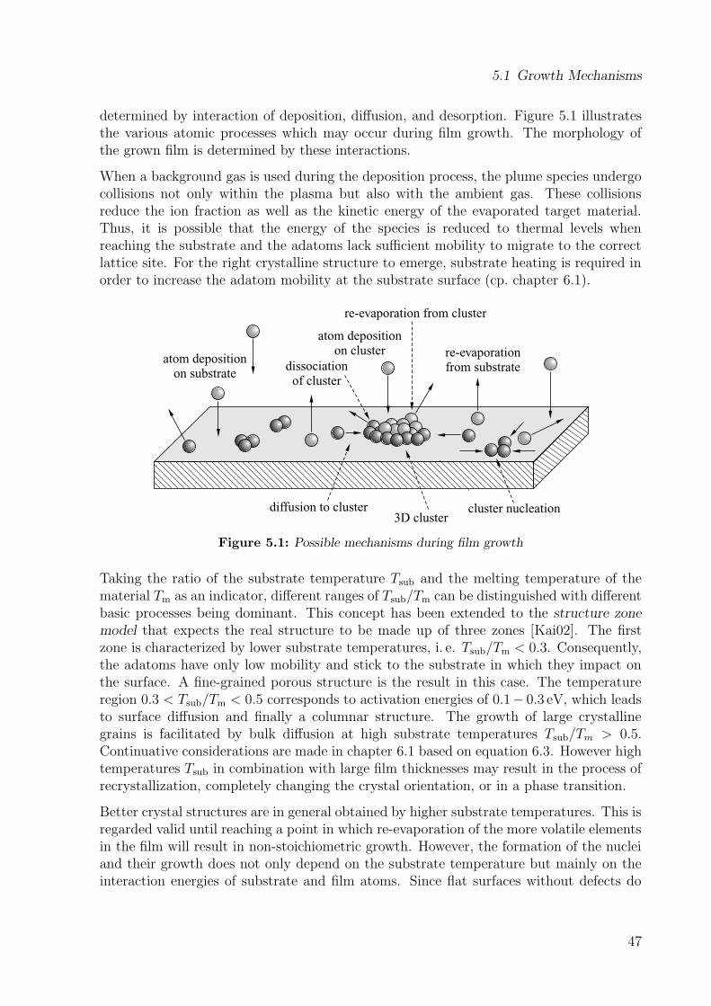
5.1 Growth Mechanisms
determined by interaction of deposition, diffusion, and desorption. Figure 5.1 illustratesthe various atomic processes which may occur during film growth. The morphology ofthe grown film is determined by these interactions.
When a background gas is used during the deposition process, the plume species undergocollisions not only within the plasma but also with the ambient gas. These collisionsreduce the ion fraction as well as the kinetic energy of the evaporated target material.Thus, it is possible that the energy of the species is reduced to thermal levels whenreaching the substrate and the adatoms lack sufficient mobility to migrate to the correctlattice site. For the right crystalline structure to emerge, substrate heating is required inorder to increase the adatom mobility at the substrate surface (cp. chapter 6.1).
diffusion to cluster3D cluster
cluster nucleation
dissociationof cluster
atom depositionon cluster
atom depositionon substrate
re-evaporation from cluster
re-evaporationfrom substrate
Figure 5.1: Possible mechanisms during film growth
Taking the ratio of the substrate temperature Tsub and the melting temperature of thematerial Tm as an indicator, different ranges of Tsub/Tm can be distinguished with differentbasic processes being dominant. This concept has been extended to the structure zone
model that expects the real structure to be made up of three zones [Kai02]. The firstzone is characterized by lower substrate temperatures, i. e. Tsub/Tm < 0.3. Consequently,the adatoms have only low mobility and stick to the substrate in which they impact onthe surface. A fine-grained porous structure is the result in this case. The temperatureregion 0.3 < Tsub/Tm < 0.5 corresponds to activation energies of 0.1− 0.3 eV, which leadsto surface diffusion and finally a columnar structure. The growth of large crystallinegrains is facilitated by bulk diffusion at high substrate temperatures Tsub/Tm > 0.5.Continuative considerations are made in chapter 6.1 based on equation 6.3. However hightemperatures Tsub in combination with large film thicknesses may result in the process ofrecrystallization, completely changing the crystal orientation, or in a phase transition.
Better crystal structures are in general obtained by higher substrate temperatures. This isregarded valid until reaching a point in which re-evaporation of the more volatile elementsin the film will result in non-stoichiometric growth. However, the formation of the nucleiand their growth does not only depend on the substrate temperature but mainly on theinteraction energies of substrate and film atoms. Since flat surfaces without defects do
47
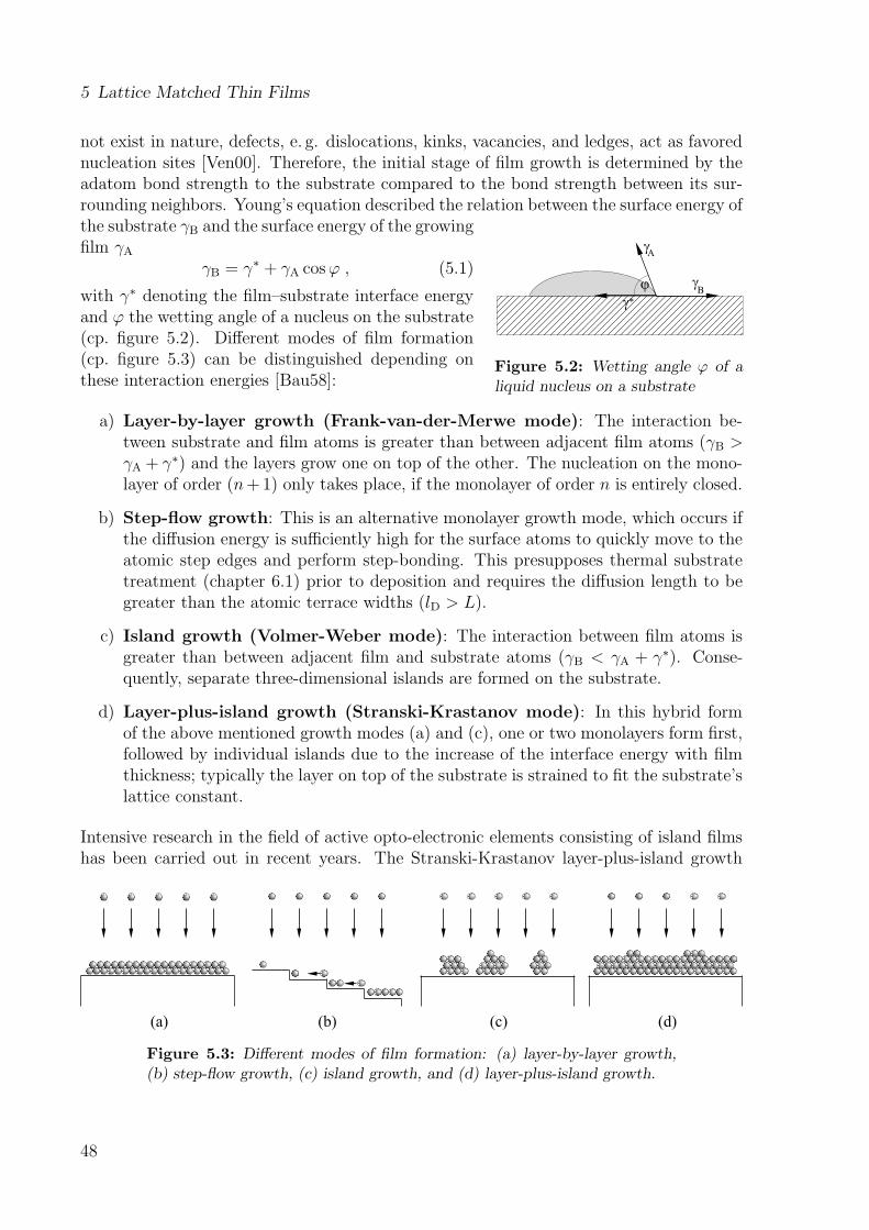
5 Lattice Matched Thin Films
not exist in nature, defects, e. g. dislocations, kinks, vacancies, and ledges, act as favorednucleation sites [Ven00]. Therefore, the initial stage of film growth is determined by theadatom bond strength to the substrate compared to the bond strength between its sur-rounding neighbors. Young’s equation described the relation between the surface energy of
j
g
g
g
A
B
*
Figure 5.2: Wetting angle ϕ of aliquid nucleus on a substrate
the substrate γB and the surface energy of the growingfilm γA
γB = γ∗ + γA cosϕ , (5.1)
with γ∗ denoting the film–substrate interface energyand ϕ the wetting angle of a nucleus on the substrate(cp. figure 5.2). Different modes of film formation(cp. figure 5.3) can be distinguished depending onthese interaction energies [Bau58]:
a) Layer-by-layer growth (Frank-van-der-Merwe mode): The interaction be-tween substrate and film atoms is greater than between adjacent film atoms (γB >γA + γ∗) and the layers grow one on top of the other. The nucleation on the mono-layer of order (n+1) only takes place, if the monolayer of order n is entirely closed.
b) Step-flow growth: This is an alternative monolayer growth mode, which occurs ifthe diffusion energy is sufficiently high for the surface atoms to quickly move to theatomic step edges and perform step-bonding. This presupposes thermal substratetreatment (chapter 6.1) prior to deposition and requires the diffusion length to begreater than the atomic terrace widths (lD > L).
c) Island growth (Volmer-Weber mode): The interaction between film atoms isgreater than between adjacent film and substrate atoms (γB < γA + γ∗). Conse-quently, separate three-dimensional islands are formed on the substrate.
d) Layer-plus-island growth (Stranski-Krastanov mode): In this hybrid formof the above mentioned growth modes (a) and (c), one or two monolayers form first,followed by individual islands due to the increase of the interface energy with filmthickness; typically the layer on top of the substrate is strained to fit the substrate’slattice constant.
Intensive research in the field of active opto-electronic elements consisting of island filmshas been carried out in recent years. The Stranski-Krastanov layer-plus-island growth
(a) (b) (d)(c)
Figure 5.3: Different modes of film formation: (a) layer-by-layer growth,(b) step-flow growth, (c) island growth, and (d) layer-plus-island growth.
48
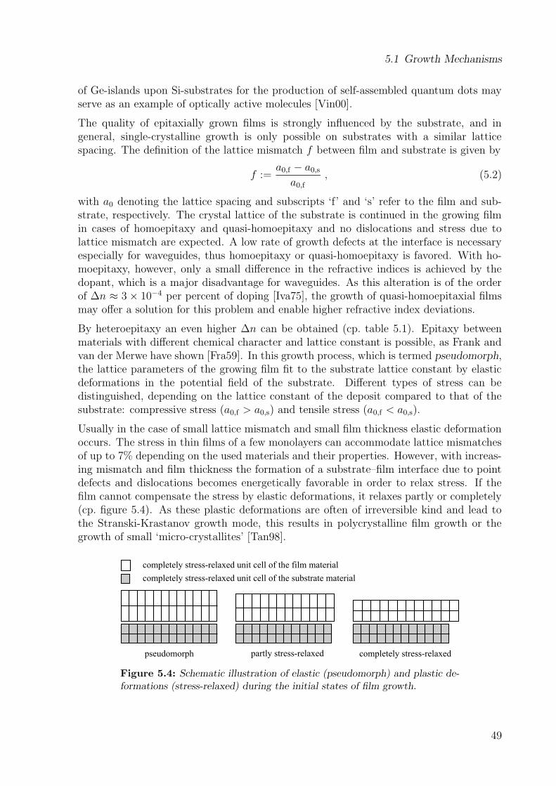
5.1 Growth Mechanisms
of Ge-islands upon Si-substrates for the production of self-assembled quantum dots mayserve as an example of optically active molecules [Vin00].
The quality of epitaxially grown films is strongly influenced by the substrate, and ingeneral, single-crystalline growth is only possible on substrates with a similar latticespacing. The definition of the lattice mismatch f between film and substrate is given by
f :=a0,f − a0,s
a0,f, (5.2)
with a0 denoting the lattice spacing and subscripts ‘f’ and ‘s’ refer to the film and sub-strate, respectively. The crystal lattice of the substrate is continued in the growing filmin cases of homoepitaxy and quasi-homoepitaxy and no dislocations and stress due tolattice mismatch are expected. A low rate of growth defects at the interface is necessaryespecially for waveguides, thus homoepitaxy or quasi-homoepitaxy is favored. With ho-moepitaxy, however, only a small difference in the refractive indices is achieved by thedopant, which is a major disadvantage for waveguides. As this alteration is of the orderof ∆n ≈ 3× 10⁻⁴ per percent of doping [Iva75], the growth of quasi-homoepitaxial filmsmay offer a solution for this problem and enable higher refractive index deviations.
By heteroepitaxy an even higher ∆n can be obtained (cp. table 5.1). Epitaxy betweenmaterials with different chemical character and lattice constant is possible, as Frank andvan der Merwe have shown [Fra59]. In this growth process, which is termed pseudomorph,the lattice parameters of the growing film fit to the substrate lattice constant by elasticdeformations in the potential field of the substrate. Different types of stress can bedistinguished, depending on the lattice constant of the deposit compared to that of thesubstrate: compressive stress (a0,f > a0,s) and tensile stress (a0,f < a0,s).
Usually in the case of small lattice mismatch and small film thickness elastic deformationoccurs. The stress in thin films of a few monolayers can accommodate lattice mismatchesof up to 7% depending on the used materials and their properties. However, with increas-ing mismatch and film thickness the formation of a substrate–film interface due to pointdefects and dislocations becomes energetically favorable in order to relax stress. If thefilm cannot compensate the stress by elastic deformations, it relaxes partly or completely(cp. figure 5.4). As these plastic deformations are often of irreversible kind and lead tothe Stranski-Krastanov growth mode, this results in polycrystalline film growth or thegrowth of small ‘micro-crystallites’ [Tan98].
pseudomorph partly stress-relaxed completely stress-relaxed
completely stress-relaxed unit cell of the film material
completely stress-relaxed unit cell of the substrate material
Figure 5.4: Schematic illustration of elastic (pseudomorph) and plastic de-formations (stress-relaxed) during the initial states of film growth.
49
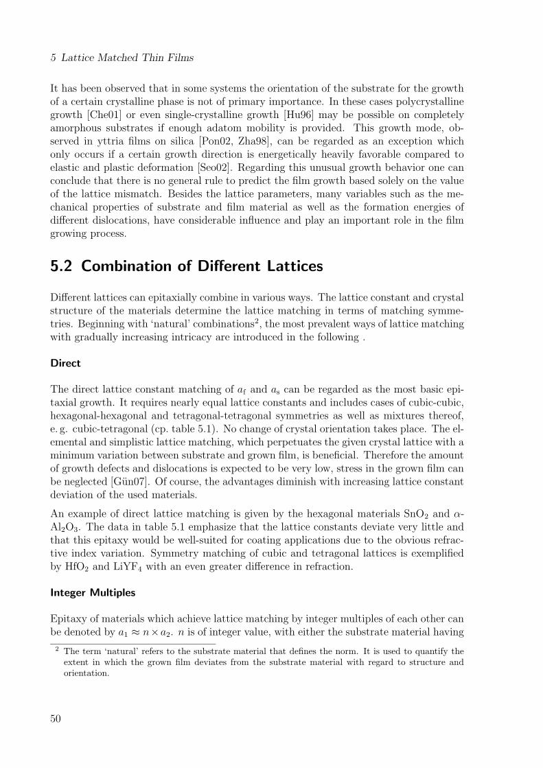
5 Lattice Matched Thin Films
It has been observed that in some systems the orientation of the substrate for the growthof a certain crystalline phase is not of primary importance. In these cases polycrystallinegrowth [Che01] or even single-crystalline growth [Hu96] may be possible on completelyamorphous substrates if enough adatom mobility is provided. This growth mode, ob-served in yttria films on silica [Pon02, Zha98], can be regarded as an exception whichonly occurs if a certain growth direction is energetically heavily favorable compared toelastic and plastic deformation [Seo02]. Regarding this unusual growth behavior one canconclude that there is no general rule to predict the film growth based solely on the valueof the lattice mismatch. Besides the lattice parameters, many variables such as the me-chanical properties of substrate and film material as well as the formation energies ofdifferent dislocations, have considerable influence and play an important role in the filmgrowing process.
5.2 Combination of Different Lattices
Different lattices can epitaxially combine in various ways. The lattice constant and crystalstructure of the materials determine the lattice matching in terms of matching symme-tries. Beginning with ‘natural’ combinations2, the most prevalent ways of lattice matchingwith gradually increasing intricacy are introduced in the following .
Direct
The direct lattice constant matching of af and as can be regarded as the most basic epi-taxial growth. It requires nearly equal lattice constants and includes cases of cubic-cubic,hexagonal-hexagonal and tetragonal-tetragonal symmetries as well as mixtures thereof,e. g. cubic-tetragonal (cp. table 5.1). No change of crystal orientation takes place. The el-emental and simplistic lattice matching, which perpetuates the given crystal lattice with aminimum variation between substrate and grown film, is beneficial. Therefore the amountof growth defects and dislocations is expected to be very low, stress in the grown film canbe neglected [Gun07]. Of course, the advantages diminish with increasing lattice constantdeviation of the used materials.
An example of direct lattice matching is given by the hexagonal materials SnO2 and α-Al2O3. The data in table 5.1 emphasize that the lattice constants deviate very little andthat this epitaxy would be well-suited for coating applications due to the obvious refrac-tive index variation. Symmetry matching of cubic and tetragonal lattices is exemplifiedby HfO2 and LiYF4 with an even greater difference in refraction.
Integer Multiples
Epitaxy of materials which achieve lattice matching by integer multiples of each other canbe denoted by a1 ≈ n×a2. n is of integer value, with either the substrate material having
2 The term ‘natural’ refers to the substrate material that defines the norm. It is used to quantify theextent in which the grown film deviates from the substrate material with regard to structure andorientation.
50
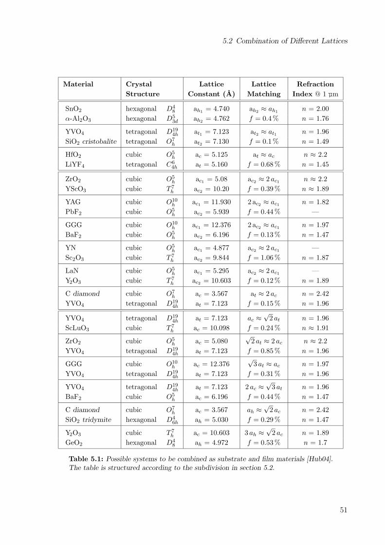
5.2 Combination of Different Lattices
Material Crystal Lattice Lattice Refraction
Structure Constant (A) Matching Index @ 1 � m
SnO2 hexagonal D48 ah1
= 4.740 ah2≈ ah1
n = 2.00
α-Al2O3 hexagonal D53d ah2
= 4.762 f = 0.4% n = 1.76
YVO4 tetragonal D194h at1 = 7.123 at2 ≈ at1 n = 1.96
SiO2 cristobalite tetragonal O7h at2 = 7.130 f = 0.1% n = 1.49
HfO2 cubic O5h ac = 5.125 at ≈ ac n ≈ 2.2
LiYF4 tetragonal C64h at = 5.160 f = 0.68% n = 1.45
ZrO2 cubic O5h ac1 = 5.08 ac2 ≈ 2 ac1 n ≈ 2.2
YScO3 cubic T 7h ac2 = 10.20 f = 0.39% n ≈ 1.89
YAG cubic O10h ac1 = 11.930 2 ac2 ≈ ac1 n = 1.82
PbF2 cubic O5h ac2 = 5.939 f = 0.44% —
GGG cubic O10h ac1 = 12.376 2 ac2 ≈ ac1 n = 1.97
BaF2 cubic O5h ac2 = 6.196 f = 0.13% n = 1.47
YN cubic O5h ac1 = 4.877 ac2 ≈ 2 ac1 —
Sc2O3 cubic T 7h ac2 = 9.844 f = 1.06% n = 1.87
LaN cubic O5h ac1 = 5.295 ac2 ≈ 2 ac1 —
Y2O3 cubic T 7h ac2 = 10.603 f = 0.12% n = 1.89
C diamond cubic O7h ac = 3.567 at ≈ 2 ac n = 2.42
YVO4 tetragonal D194h at = 7.123 f = 0.15% n = 1.96
YVO4 tetragonal D194h at = 7.123 ac ≈
√2 at n = 1.96
ScLuO3 cubic T 7h ac = 10.098 f = 0.24% n ≈ 1.91
ZrO2 cubic O5h ac = 5.080
√2 at ≈ 2 ac n ≈ 2.2
YVO4 tetragonal D194h at = 7.123 f = 0.85% n = 1.96
GGG cubic O10h ac = 12.376
√3 at ≈ ac n = 1.97
YVO4 tetragonal D194h at = 7.123 f = 0.31% n = 1.96
YVO4 tetragonal D194h at = 7.123 2 ac ≈
√3 at n = 1.96
BaF2 cubic O5h ac = 6.196 f = 0.44% n = 1.47
C diamond cubic O7h ac = 3.567 ah ≈
√2 ac n = 2.42
SiO2 tridymite hexagonal D46h ah = 5.030 f = 0.29% n = 1.47
Y2O3 cubic T 7h ac = 10.603 3 ah ≈
√2 ac n = 1.89
GeO2 hexagonal D48 ah = 4.972 f = 0.53% n = 1.7
Table 5.1: Possible systems to be combined as substrate and film materials [Hub04].The table is structured according to the subdivision in section 5.2.
51
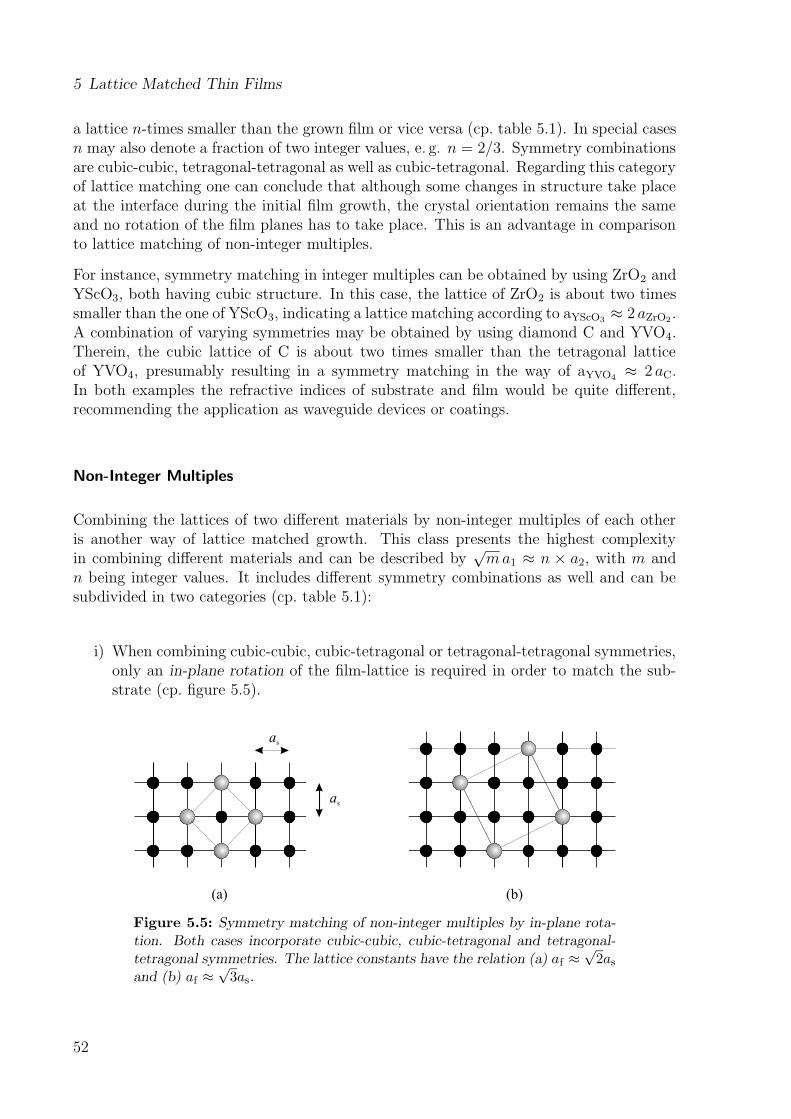
5 Lattice Matched Thin Films
a lattice n-times smaller than the grown film or vice versa (cp. table 5.1). In special casesn may also denote a fraction of two integer values, e. g. n = 2/3. Symmetry combinationsare cubic-cubic, tetragonal-tetragonal as well as cubic-tetragonal. Regarding this categoryof lattice matching one can conclude that although some changes in structure take placeat the interface during the initial film growth, the crystal orientation remains the sameand no rotation of the film planes has to take place. This is an advantage in comparisonto lattice matching of non-integer multiples.
For instance, symmetry matching in integer multiples can be obtained by using ZrO2 andYScO3, both having cubic structure. In this case, the lattice of ZrO2 is about two timessmaller than the one of YScO3, indicating a lattice matching according to aYScO3
≈ 2 aZrO2.
A combination of varying symmetries may be obtained by using diamond C and YVO4.Therein, the cubic lattice of C is about two times smaller than the tetragonal latticeof YVO4, presumably resulting in a symmetry matching in the way of aYVO4
≈ 2 aC.In both examples the refractive indices of substrate and film would be quite different,recommending the application as waveguide devices or coatings.
Non-Integer Multiples
Combining the lattices of two different materials by non-integer multiples of each otheris another way of lattice matched growth. This class presents the highest complexityin combining different materials and can be described by
√ma1 ≈ n × a2, with m and
n being integer values. It includes different symmetry combinations as well and can besubdivided in two categories (cp. table 5.1):
i) When combining cubic-cubic, cubic-tetragonal or tetragonal-tetragonal symmetries,only an in-plane rotation of the film-lattice is required in order to match the sub-strate (cp. figure 5.5).
(a) (b)
as
as
Figure 5.5: Symmetry matching of non-integer multiples by in-plane rota-tion. Both cases incorporate cubic-cubic, cubic-tetragonal and tetragonal-tetragonal symmetries. The lattice constants have the relation (a) af ≈
√2as
and (b) af ≈√3as.
52
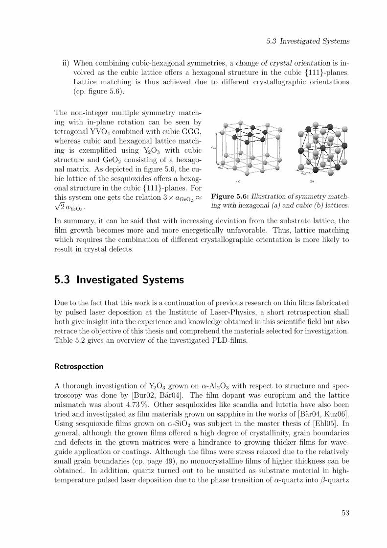
5.3 Investigated Systems
ii) When combining cubic-hexagonal symmetries, a change of crystal orientation is in-volved as the cubic lattice offers a hexagonal structure in the cubic {111}-planes.Lattice matching is thus achieved due to different crystallographic orientations(cp. figure 5.6).
(a) (b)
ahex
chex
acub
Figure 5.6: Illustration of symmetry match-ing with hexagonal (a) and cubic (b) lattices.
The non-integer multiple symmetry match-ing with in-plane rotation can be seen bytetragonal YVO4 combined with cubic GGG,whereas cubic and hexagonal lattice match-ing is exemplified using Y2O3 with cubicstructure and GeO2 consisting of a hexago-nal matrix. As depicted in figure 5.6, the cu-bic lattice of the sesquioxides offers a hexag-onal structure in the cubic {111}-planes. Forthis system one gets the relation 3×aGeO2
≈√2 aY2O3
.
In summary, it can be said that with increasing deviation from the substrate lattice, thefilm growth becomes more and more energetically unfavorable. Thus, lattice matchingwhich requires the combination of different crystallographic orientation is more likely toresult in crystal defects.
5.3 Investigated Systems
Due to the fact that this work is a continuation of previous research on thin films fabricatedby pulsed laser deposition at the Institute of Laser-Physics, a short retrospection shallboth give insight into the experience and knowledge obtained in this scientific field but alsoretrace the objective of this thesis and comprehend the materials selected for investigation.Table 5.2 gives an overview of the investigated PLD-films.
Retrospection
A thorough investigation of Y2O3 grown on α-Al2O3 with respect to structure and spec-troscopy was done by [Bur02, Bar04]. The film dopant was europium and the latticemismatch was about 4.73%. Other sesquioxides like scandia and lutetia have also beentried and investigated as film materials grown on sapphire in the works of [Bar04, Kuz06].Using sesquioxide films grown on α-SiO2 was subject in the master thesis of [Ehl05]. Ingeneral, although the grown films offered a high degree of crystallinity, grain boundariesand defects in the grown matrices were a hindrance to growing thicker films for wave-guide application or coatings. Although the films were stress relaxed due to the relativelysmall grain boundaries (cp. page 49), no monocrystalline films of higher thickness can beobtained. In addition, quartz turned out to be unsuited as substrate material in high-temperature pulsed laser deposition due to the phase transition of α-quartz into β-quartz
53
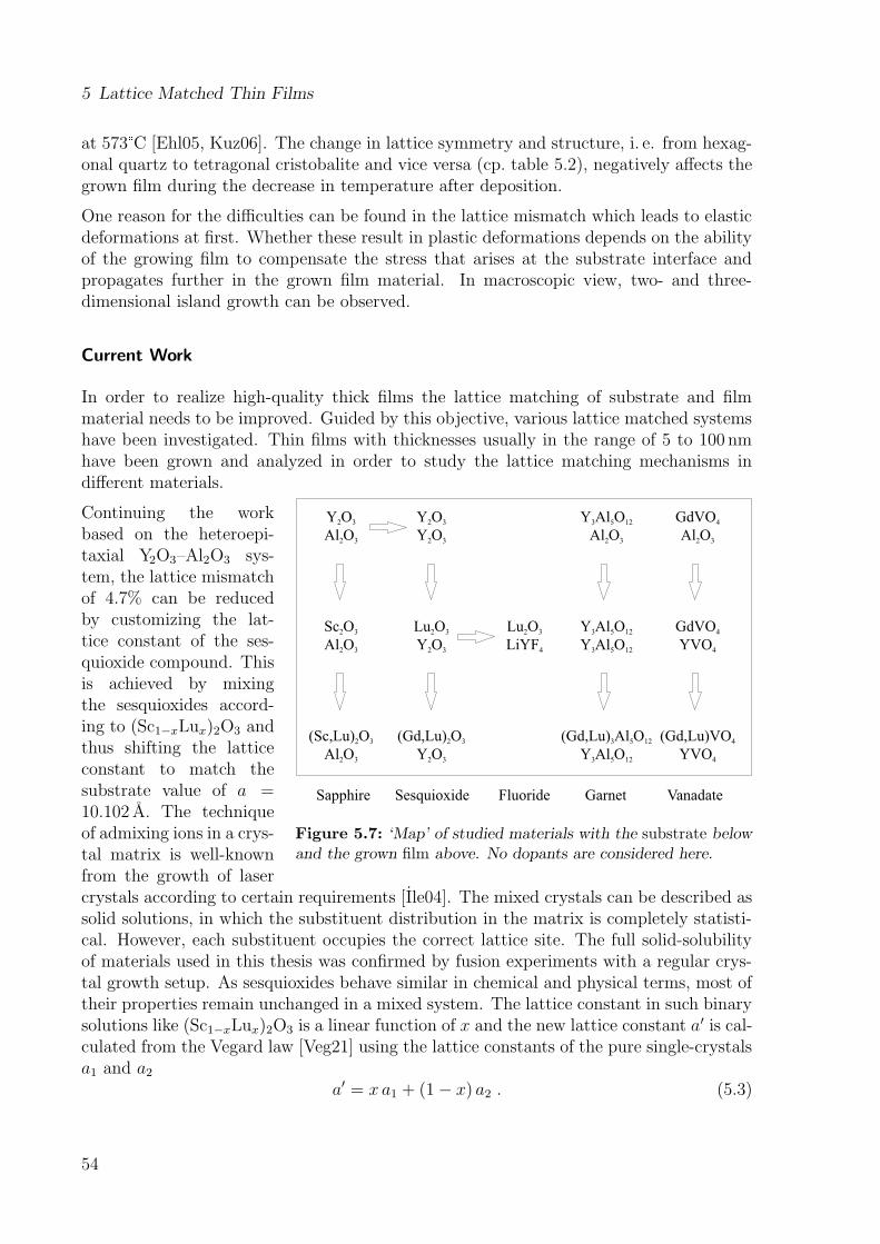
5 Lattice Matched Thin Films
at 573 � C [Ehl05, Kuz06]. The change in lattice symmetry and structure, i. e. from hexag-onal quartz to tetragonal cristobalite and vice versa (cp. table 5.2), negatively affects thegrown film during the decrease in temperature after deposition.
One reason for the difficulties can be found in the lattice mismatch which leads to elasticdeformations at first. Whether these result in plastic deformations depends on the abilityof the growing film to compensate the stress that arises at the substrate interface andpropagates further in the grown film material. In macroscopic view, two- and three-dimensional island growth can be observed.
Current Work
In order to realize high-quality thick films the lattice matching of substrate and filmmaterial needs to be improved. Guided by this objective, various lattice matched systemshave been investigated. Thin films with thicknesses usually in the range of 5 to 100 nmhave been grown and analyzed in order to study the lattice matching mechanisms in
Y O
Al O2 3
2 3
Sc O
Al O2 3
2 3
(Sc,Lu) O
Al O2 3
2 3
Y O2 3
Y O2 3
Lu O
Y O2 3
2 3
(Gd,Lu) O
Y O2 3
2 3
Lu O
LiYF2 3
4
3 5 12
2 3
Y Al O
Al O
Sapphire Sesquioxide Fluoride Garnet Vanadate
4
2 3
GdVO
Al O
Y Al O
Y Al O3 5 12
3 5 12
(Gd,Lu) Al O
Y Al O3 5 12
3 5 12
4
4
GdVO
YVO
(Gd,Lu)VO
YVO4
4
Figure 5.7: ‘Map’ of studied materials with the substrate belowand the grown film above. No dopants are considered here.
different materials.
Continuing the workbased on the heteroepi-taxial Y2O3–Al2O3 sys-tem, the lattice mismatchof 4.7% can be reducedby customizing the lat-tice constant of the ses-quioxide compound. Thisis achieved by mixingthe sesquioxides accord-ing to (Sc1−xLux)2O3 andthus shifting the latticeconstant to match thesubstrate value of a =10.102 A. The techniqueof admixing ions in a crys-tal matrix is well-knownfrom the growth of lasercrystals according to certain requirements [Ile04]. The mixed crystals can be described assolid solutions, in which the substituent distribution in the matrix is completely statisti-cal. However, each substituent occupies the correct lattice site. The full solid-solubilityof materials used in this thesis was confirmed by fusion experiments with a regular crys-tal growth setup. As sesquioxides behave similar in chemical and physical terms, most oftheir properties remain unchanged in a mixed system. The lattice constant in such binarysolutions like (Sc1−xLux)2O3 is a linear function of x and the new lattice constant a′ is cal-culated from the Vegard law [Veg21] using the lattice constants of the pure single-crystalsa1 and a2
a′ = x a1 + (1− x) a2 . (5.3)
54
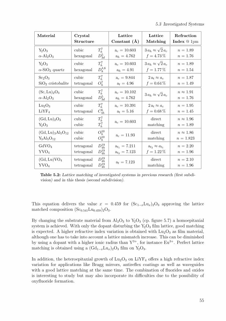
5.3 Investigated Systems
Material Crystal Lattice Lattice Refraction
Structure Constant (A) Matching Index @ 1 � m
Y2O3 cubic T 7h ac = 10.603 3 ah ≈
√2 ac n = 1.89
α-Al2O3 hexagonal D53d ah = 4.762 f = 4.73% n = 1.76
Y2O3 cubic T 7h ac = 10.603 3 ah ≈
√2 ac n = 1.89
α-SiO2 quartz hexagonal D4,68 ah = 4.91 f = 1.77% n = 1.54
Sc2O3 cubic T 7h ac = 9.844 2 at ≈ ac n = 1.87
SiO2 cristobalite tetragonal O7h at = 4.96 f = 0.64% n = 1.49
(Sc, Lu)2O3 cubic T 7h ac = 10.102 3 ah ≈
√2 ac
n ≈ 1.91α-Al2O3 hexagonal D5
3d ah = 4.762 n = 1.76
Lu2O3 cubic T 7h ac = 10.391 2 at ≈ ac n = 1.95
LiYF4 tetragonal C64h at = 5.16 f = 0.68% n = 1.45
(Gd, Lu)2O3 cubic T 7h ac = 10.603
direct n ≈ 1.96Y2O3 cubic T 7
h matching n = 1.89
(Gd, Lu)3Al5O12 cubic O10h ac = 11.93
direct n ≈ 1.86Y3Al5O12 cubic O10
h matching n = 1.823
GdVO4 tetragonal D194h at1 = 7.211 at2 ≈ at1 n = 2.20
YVO4 tetragonal D194h at2 = 7.123 f = 1.22% n = 1.96
(Gd, Lu)VO4 tetragonal D194h at = 7.123
direct n = 2.10
YVO4 tetragonal D194h matching n = 1.96
Table 5.2: Lattice matching of investigated systems in previous research (first subdi-vision) and in this thesis (second subdivision).
This equation delivers the value x = 0.459 for (Sc1−xLux)2O3 approving the latticematched composition (Sc0.541Lu0.459)2O3.
By changing the substrate material from Al2O3 to Y2O3 (cp. figure 5.7) a homoepitaxialsystem is achieved. With only the dopant disturbing the Y2O3 film lattice, good matchingis expected. A higher refractive index variation is obtained with Lu2O3 as film material,although one has to take into account a lattice mismatch increase. This can be diminishedby using a dopant with a higher ionic radius than Y3+, for instance Eu3+. Perfect latticematching is obtained using a (Gd1−xLux)2O3 film on Y2O3.
In addition, the heteroepitaxial growth of Lu2O3 on LiYF4 offers a high refractive indexvariation for applications like Bragg mirrors, antireflex coatings as well as waveguideswith a good lattice matching at the same time. The combination of fluorides and oxidesis interesting to study but may also incorporate its difficulties due to the possibility ofoxyfluoride formation.
55

5 Lattice Matched Thin Films
Other homo- and quasi-homoepitaxial films based on garnet- and vanadate-materials havebeen fabricated and characterized. Each of them has been fabricated non-lattice matchedby the growth on sapphire in order to estimate the film deposition rate (cp. appendix A).Then the lattice mismatch has gradually been decreased, first by moving to homoepitaxialgrowth and then to a quasi-homoepitaxial lattice matched film. The last step has alwaysbeen achieved by admixing gadolinium and lutetium to match the equivalent yttrium-based substrate material (cp. figure 5.7).
56
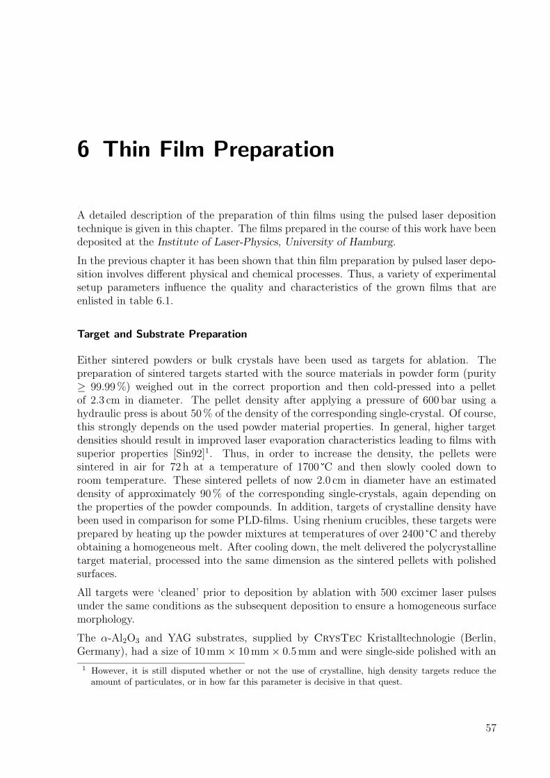
6 Thin Film Preparation
A detailed description of the preparation of thin films using the pulsed laser depositiontechnique is given in this chapter. The films prepared in the course of this work have beendeposited at the Institute of Laser-Physics, University of Hamburg.
In the previous chapter it has been shown that thin film preparation by pulsed laser depo-sition involves different physical and chemical processes. Thus, a variety of experimentalsetup parameters influence the quality and characteristics of the grown films that areenlisted in table 6.1.
Target and Substrate Preparation
Either sintered powders or bulk crystals have been used as targets for ablation. Thepreparation of sintered targets started with the source materials in powder form (purity≥ 99.99%) weighed out in the correct proportion and then cold-pressed into a pelletof 2.3 cm in diameter. The pellet density after applying a pressure of 600 bar using ahydraulic press is about 50% of the density of the corresponding single-crystal. Of course,this strongly depends on the used powder material properties. In general, higher targetdensities should result in improved laser evaporation characteristics leading to films withsuperior properties [Sin92]1. Thus, in order to increase the density, the pellets weresintered in air for 72 h at a temperature of 1700 � C and then slowly cooled down toroom temperature. These sintered pellets of now 2.0 cm in diameter have an estimateddensity of approximately 90% of the corresponding single-crystals, again depending onthe properties of the powder compounds. In addition, targets of crystalline density havebeen used in comparison for some PLD-films. Using rhenium crucibles, these targets wereprepared by heating up the powder mixtures at temperatures of over 2400 � C and therebyobtaining a homogeneous melt. After cooling down, the melt delivered the polycrystallinetarget material, processed into the same dimension as the sintered pellets with polishedsurfaces.
All targets were ‘cleaned’ prior to deposition by ablation with 500 excimer laser pulsesunder the same conditions as the subsequent deposition to ensure a homogeneous surfacemorphology.
The α-Al2O3 and YAG substrates, supplied by CrysTec Kristalltechnologie (Berlin,Germany), had a size of 10mm× 10mm× 0.5mm and were single-side polished with an
1 However, it is still disputed whether or not the use of crystalline, high density targets reduce theamount of particulates, or in how far this parameter is decisive in that quest.
57
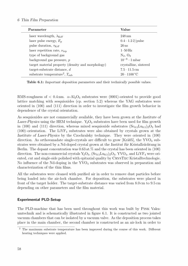
6 Thin Film Preparation
Parameter Value
laser wavelength, λKrF 248 nm
laser pulse energy, Ep 0.4 – 1.2 J/pulse
pulse duration, τKrF 20 ns
laser repetition rate, νrep 1–50Hz
type of background gas N2, O2
background gas pressure, p 10−8 – 1mbar
target material property (density and morphology) crystalline, sintered
target-substrate distance, d 7.5 – 11.5 cm
substrate temperature2, Tsub 20 – 1100 � C
Table 6.1: Important deposition parameters and their technically possible values.
RMS-roughness of < 0.4 nm. α-Al2O3 substrates were 〈0001〉-oriented to provide goodlattice matching with sesquioxides (cp. section 5.2) whereas the YAG substrates wereoriented in 〈100〉 and 〈111〉 direction in order to investigate the film growth behavior independence of the crystal orientation.
As sesquioxides are not commercially available, they have been grown at the Institute of
Laser-Physics using the HEM technique. Y2O3 substrates have been used for film growthin 〈100〉 and 〈111〉 direction, whereas mixed sesquioxide substrates (Sc0.5Lu0.5)2O3 had(100) -orientation. The LiYF4 substrates were also obtained by crystals grown at theInstitute of Laser-Physics by the Czochralsky technique. They were oriented in 〈100〉direction. As orthovanadate single-crystals are difficult to grow [Kra05], the YVO4 sub-strates were obtained by a Nd-doped crystal grown at the Institut fur Kristallzuchtung inBerlin. The dopant concentration was 0.63 at.% and the crystal has been oriented in 〈100〉direction. The non-commercial crystals Y2O3, (Sc0.5Lu0.5)2O3, YVO4, and LiYF4 were ori-ented, cut and single-side polished with epitaxial quality by CrysTec Kristalltechnologie.No influence of the Nd-doping in the YVO4 substrates was observed in preparation andcharacterization of the thin films.
All the substrates were cleaned with purified air in order to remove dust particles beforebeing loaded into the air-lock chamber. For deposition, the substrates were placed infront of the target holder. The target-substrate distance was varied from 8.0 cm to 9.5 cmdepending on other parameters and the film material.
Experimental PLD-Setup
The PLD-machine that has been used throughout this work was built by Pink Vaku-umtechnik and is schematically illustrated in figure 6.1. It is constructed as two jointedvacuum chambers that can be isolated by a vacuum valve. As the deposition process takesplace in the main chamber, the second chamber is constructed as an air-lock in order to
2 The maximum substrate temperature has been improved during the course of this work. Differentheating techniques were applied.
58
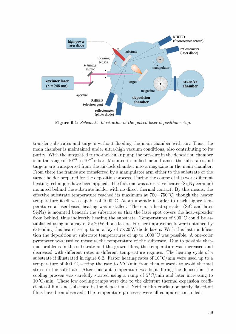
RHEED(electron gun)
RHEED(fluorescence screen)
manipulator
magazine
reflectometer(photo diode)
target
substrate
high-powerlaser diode
scanningmirror
depositionchamber
reflectometer(laser diode)
transferchamber
aperture
focusinglenses
excimer laser
( = 248 nm)l
q
Figure 6.1: Schematic illustration of the pulsed laser deposition setup.
transfer substrates and targets without flooding the main chamber with air. Thus, themain chamber is maintained under ultra-high vacuum conditions, also contributing to itspurity. With the integrated turbo-molecular pump the pressure in the deposition chamberis in the range of 10−8 to 10−7mbar. Mounted in unified metal frames, the substrates andtargets are transported from the air-lock chamber into a magazine in the main chamber.From there the frames are transferred by a manipulator arm either to the substrate or thetarget holder prepared for the deposition process. During the course of this work differentheating techniques have been applied. The first one was a resistive heater (Si3N4-ceramic)mounted behind the substrate holder with no direct thermal contact. By this means, theeffective substrate temperature reached its maximum at 700 – 750 � C, though the heatertemperature itself was capable of 1000 � C. As an upgrade in order to reach higher tem-peratures a laser-based heating was installed. Therein, a heat-spreader (SiC and laterSi3N4) is mounted beneath the substrate so that the laser spot covers the heat-spreaderfrom behind, thus indirectly heating the substrate. Temperatures of 900 � C could be es-tablished using an array of 5×20W diode lasers. Further improvements were obtained byextending this heater setup to an array of 7×20W diode lasers. With this last modifica-tion the deposition at substrate temperatures of up to 1000 � C was possible. A one-colorpyrometer was used to measure the temperature of the substrate. Due to possible ther-mal problems in the substrate and the grown films, the temperature was increased anddecreased with different rates in different temperature regimes. The heating cycle of asubstrate if illustrated in figure 6.2. Faster heating rates of 10 � C/min were used up to atemperature of 400 � C, setting the rate to 5 � C/min from then onwards to avoid thermalstress in the substrate. After constant temperature was kept during the deposition, thecooling process was carefully started using a ramp of 5 � C/min and later increasing to10 � C/min. These low cooling ramps were due to the different thermal expansion coeffi-cients of film and substrate in the depositions. Neither film cracks nor partly flaked-offfilms have been observed. The temperature processes were all computer-controlled.
59
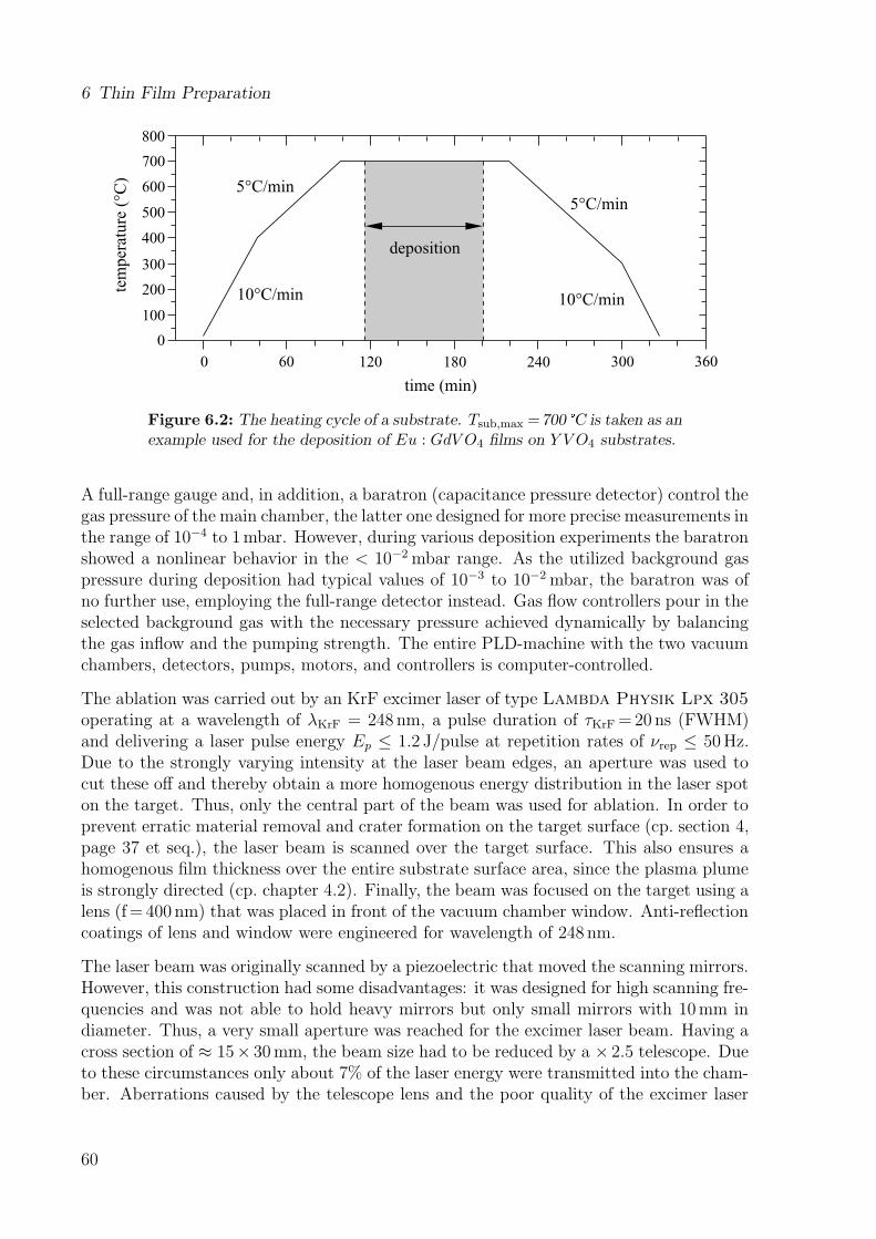
6 Thin Film Preparation
tem
pera
ture
(°C
)
deposition
10°C/min 10°C/min
5°C/min5°C/min
time (min)
00
100
200
300
400
500
600
700
800
60 120 180 240 300 360
Figure 6.2: The heating cycle of a substrate. Tsub,max=700 � C is taken as anexample used for the deposition of Eu : GdV O4 films on Y V O4 substrates.
A full-range gauge and, in addition, a baratron (capacitance pressure detector) control thegas pressure of the main chamber, the latter one designed for more precise measurements inthe range of 10−4 to 1mbar. However, during various deposition experiments the baratronshowed a nonlinear behavior in the < 10−2mbar range. As the utilized background gaspressure during deposition had typical values of 10−3 to 10−2mbar, the baratron was ofno further use, employing the full-range detector instead. Gas flow controllers pour in theselected background gas with the necessary pressure achieved dynamically by balancingthe gas inflow and the pumping strength. The entire PLD-machine with the two vacuumchambers, detectors, pumps, motors, and controllers is computer-controlled.
The ablation was carried out by an KrF excimer laser of type Lambda Physik Lpx 305operating at a wavelength of λKrF = 248 nm, a pulse duration of τKrF=20ns (FWHM)and delivering a laser pulse energy Ep ≤ 1.2 J/pulse at repetition rates of νrep ≤ 50Hz.Due to the strongly varying intensity at the laser beam edges, an aperture was used tocut these off and thereby obtain a more homogenous energy distribution in the laser spoton the target. Thus, only the central part of the beam was used for ablation. In order toprevent erratic material removal and crater formation on the target surface (cp. section 4,page 37 et seq.), the laser beam is scanned over the target surface. This also ensures ahomogenous film thickness over the entire substrate surface area, since the plasma plumeis strongly directed (cp. chapter 4.2). Finally, the beam was focused on the target using alens (f= 400 nm) that was placed in front of the vacuum chamber window. Anti-reflectioncoatings of lens and window were engineered for wavelength of 248 nm.
The laser beam was originally scanned by a piezoelectric that moved the scanning mirrors.However, this construction had some disadvantages: it was designed for high scanning fre-quencies and was not able to hold heavy mirrors but only small mirrors with 10mm indiameter. Thus, a very small aperture was reached for the excimer laser beam. Having across section of ≈ 15× 30mm, the beam size had to be reduced by a × 2.5 telescope. Dueto these circumstances only about 7% of the laser energy were transmitted into the cham-ber. Aberrations caused by the telescope lens and the poor quality of the excimer laser
60
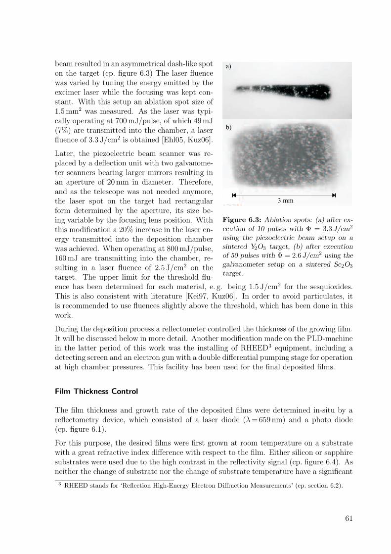
3 mm
a)
b)
Figure 6.3: Ablation spots: (a) after ex-ecution of 10 pulses with Φ = 3.3 J/cm2
using the piezoelectric beam setup on asintered Y2O3 target, (b) after executionof 50 pulses with Φ = 2.6 J/cm2 using thegalvanometer setup on a sintered Sc2O3
target.
beam resulted in an asymmetrical dash-like spoton the target (cp. figure 6.3) The laser fluencewas varied by tuning the energy emitted by theexcimer laser while the focusing was kept con-stant. With this setup an ablation spot size of1.5mm2 was measured. As the laser was typi-cally operating at 700mJ/pulse, of which 49mJ(7%) are transmitted into the chamber, a laserfluence of 3.3 J/cm2 is obtained [Ehl05, Kuz06].
Later, the piezoelectric beam scanner was re-placed by a deflection unit with two galvanome-ter scanners bearing larger mirrors resulting inan aperture of 20mm in diameter. Therefore,and as the telescope was not needed anymore,the laser spot on the target had rectangularform determined by the aperture, its size be-ing variable by the focusing lens position. Withthis modification a 20% increase in the laser en-ergy transmitted into the deposition chamberwas achieved. When operating at 800mJ/pulse,160mJ are transmitting into the chamber, re-sulting in a laser fluence of 2.5 J/cm2 on thetarget. The upper limit for the threshold flu-ence has been determined for each material, e. g. being 1.5 J/cm2 for the sesquioxides.This is also consistent with literature [Kei97, Kuz06]. In order to avoid particulates, itis recommended to use fluences slightly above the threshold, which has been done in thiswork.
During the deposition process a reflectometer controlled the thickness of the growing film.It will be discussed below in more detail. Another modification made on the PLD-machinein the latter period of this work was the installing of RHEED3 equipment, including adetecting screen and an electron gun with a double differential pumping stage for operationat high chamber pressures. This facility has been used for the final deposited films.
Film Thickness Control
The film thickness and growth rate of the deposited films were determined in-situ by areflectometry device, which consisted of a laser diode (λ=659 nm) and a photo diode(cp. figure 6.1).
For this purpose, the desired films were first grown at room temperature on a substratewith a great refractive index difference with respect to the film. Either silicon or sapphiresubstrates were used due to the high contrast in the reflectivity signal (cp. figure 6.4). Asneither the change of substrate nor the change of substrate temperature have a significant
3 RHEED stands for ‘Reflection High-Energy Electron Diffraction Measurements’ (cp. section 6.2).
61
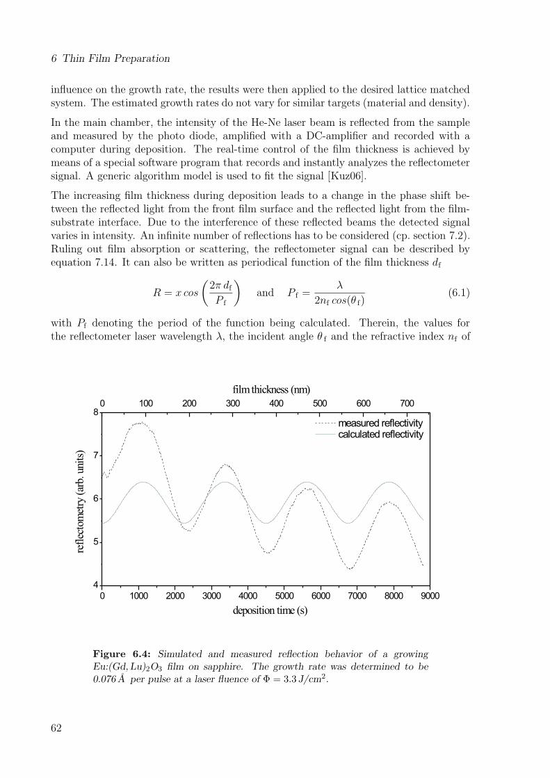
6 Thin Film Preparation
influence on the growth rate, the results were then applied to the desired lattice matchedsystem. The estimated growth rates do not vary for similar targets (material and density).
In the main chamber, the intensity of the He-Ne laser beam is reflected from the sampleand measured by the photo diode, amplified with a DC-amplifier and recorded with acomputer during deposition. The real-time control of the film thickness is achieved bymeans of a special software program that records and instantly analyzes the reflectometersignal. A generic algorithm model is used to fit the signal [Kuz06].
The increasing film thickness during deposition leads to a change in the phase shift be-tween the reflected light from the front film surface and the reflected light from the film-substrate interface. Due to the interference of these reflected beams the detected signalvaries in intensity. An infinite number of reflections has to be considered (cp. section 7.2).Ruling out film absorption or scattering, the reflectometer signal can be described byequation 7.14. It can also be written as periodical function of the film thickness df
R = x cos
(2π dfP f
)
and P f =λ
2nf cos(θ f)(6.1)
with Pf denoting the period of the function being calculated. Therein, the values forthe reflectometer laser wavelength λ, the incident angle θ f and the refractive index nf of
0 1000 2000 3000 4000 5000 6000 7000 8000 9000
4
5
6
7
80 100 200 300 400 500 600 700
film thickness (nm)
measured reflectivitycalculated reflectivity
refl
ecto
met
ry(a
rb.u
nits
)
deposition time (s)
Figure 6.4: Simulated and measured reflection behavior of a growingEu:(Gd, Lu)2O3 film on sapphire. The growth rate was determined to be0.076 A per pulse at a laser fluence of Φ = 3.3 J/cm2.
62
the film must be known. During film deposition the reflectometer signal is recorded as afunction of the excimer laser pulse number I(Np) and the measured signal is fitted usingthe relation
I = c+ aR cos
(2π ZrNp
Pf
)
(6.2)
with R being the reflectometer signal (cp. equation 7.14, page 81), c denoting a constantshift that can result from the amplifier or an incoherent reflection from the substratebackside, a being the amplitude scaling factor, and Zr representing the deposition rate.By using equation 6.2, the deposition rate Zr and thus the film thickness df = ZrNp canbe obtained by the measured signal.
An example of simulated and measured reflection behavior is presented in figure 6.4. Theintensity decay of the measured signal is due to the increasing film growth causing thereflected beam to slightly drift off the photo diode, whose detection area is only about1-2mm in diameter.
Optimization of the Pulsed Laser Deposition Process Parameters
A big advantage of the pulsed laser deposition is the flexibility of the process that en-ables various different materials to be adapted for deposition. Apart from this beneficialflexibility, the PLD is a quite complex process with many parameters that need to beoptimized for every material in order to achieve the desired high film quality. However,systematic investigations concerning the influence of PLD process parameters are rare upto now.
Research on the fabrication of Y2O3 films is found in Lancock [Lan04] as well as in thetheses of Burmester [Bur02] and Bar [Bar04]. Investigations on the deposition of gadolin-ium gallium garnet (GGG) and Ti-doped sapphire films can be found in the theses ofBarrington [Bar01] and Anderson [And98], whereas the film growth parameters of YAG,Sc2O3 and Lu2O3 are determined in the thesis of Kuzminykh [Kuz06]. Information onthe deposition of RE-doped GdVO4 films on YVO4 is given in [Bar05]. In addition, gen-eral information on deposition behavior in dependence on the process parameters can befound here. However, being a complex process, the deposition success will never dependon the ‘correct’ setup of one parameter alone, but is an interplay of all crucial depositionparameters enlisted in table 6.1. As the possibilities of lattice matching are investigatedusing different substrate and film materials, a systematic analysis of the deposition pro-cess parameters was performed for materials that have not been investigated for PLDapplication yet. If possible, the available information has been adapted and adjusted tomaterials of similar kinds.
The possibilities of lattice matching were primarily investigated by films having a max-imum thickness of 100 nm. Thus, although the target density is assumed to influencethe amount of particulates and droplets, this effect should only play a negligible roledue to the relatively thin film thicknesses. Nevertheless, high density targets (90 – 100%compared to crystal density) have been used. Crystalline targets are claimed to reduce
63
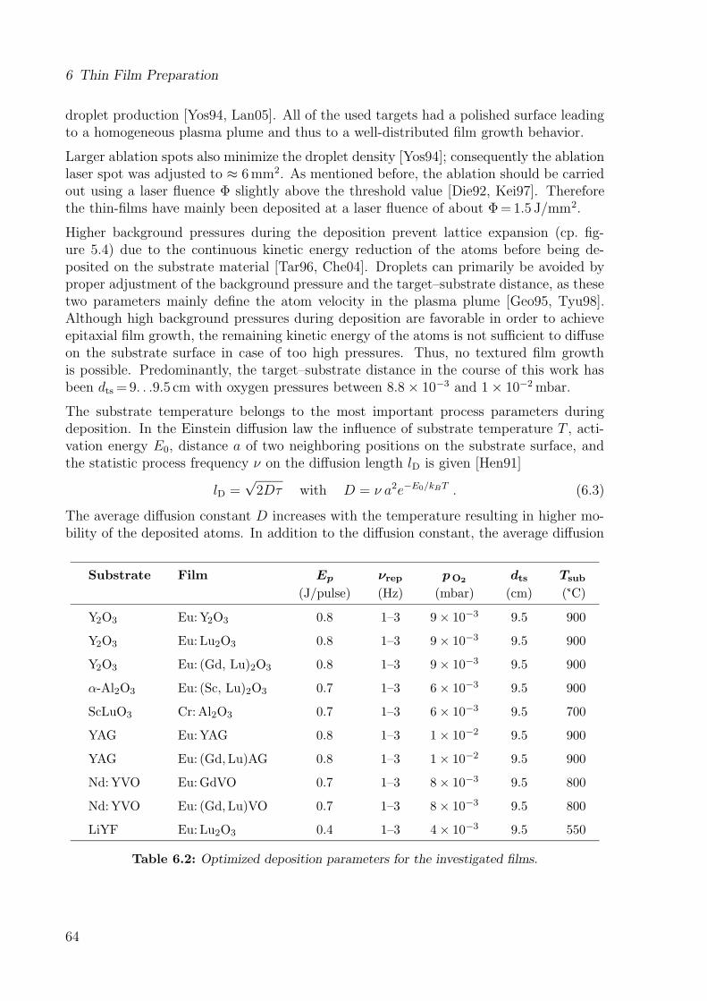
6 Thin Film Preparation
droplet production [Yos94, Lan05]. All of the used targets had a polished surface leadingto a homogeneous plasma plume and thus to a well-distributed film growth behavior.
Larger ablation spots also minimize the droplet density [Yos94]; consequently the ablationlaser spot was adjusted to ≈ 6mm2. As mentioned before, the ablation should be carriedout using a laser fluence Φ slightly above the threshold value [Die92, Kei97]. Thereforethe thin-films have mainly been deposited at a laser fluence of about Φ=1.5 J/mm2.
Higher background pressures during the deposition prevent lattice expansion (cp. fig-ure 5.4) due to the continuous kinetic energy reduction of the atoms before being de-posited on the substrate material [Tar96, Che04]. Droplets can primarily be avoided byproper adjustment of the background pressure and the target–substrate distance, as thesetwo parameters mainly define the atom velocity in the plasma plume [Geo95, Tyu98].Although high background pressures during deposition are favorable in order to achieveepitaxial film growth, the remaining kinetic energy of the atoms is not sufficient to diffuseon the substrate surface in case of too high pressures. Thus, no textured film growthis possible. Predominantly, the target–substrate distance in the course of this work hasbeen dts=9. . .9.5 cm with oxygen pressures between 8.8× 10⁻³ and 1× 10⁻²mbar.
The substrate temperature belongs to the most important process parameters duringdeposition. In the Einstein diffusion law the influence of substrate temperature T , acti-vation energy E0, distance a of two neighboring positions on the substrate surface, andthe statistic process frequency ν on the diffusion length lD is given [Hen91]
lD =√2Dτ with D = ν a2e−E0/kBT . (6.3)
The average diffusion constant D increases with the temperature resulting in higher mo-bility of the deposited atoms. In addition to the diffusion constant, the average diffusion
Substrate Film Ep νrep pO2dts Tsub
(J/pulse) (Hz) (mbar) (cm) ( � C)
Y2O3 Eu:Y2O3 0.8 1–3 9× 10⁻³ 9.5 900
Y2O3 Eu: Lu2O3 0.8 1–3 9× 10⁻³ 9.5 900
Y2O3 Eu: (Gd, Lu)2O3 0.8 1–3 9× 10⁻³ 9.5 900
α-Al2O3 Eu: (Sc, Lu)2O3 0.7 1–3 6× 10⁻³ 9.5 900
ScLuO3 Cr:Al2O3 0.7 1–3 6× 10⁻³ 9.5 700
YAG Eu:YAG 0.8 1–3 1× 10⁻² 9.5 900
YAG Eu: (Gd, Lu)AG 0.8 1–3 1× 10⁻² 9.5 900
Nd:YVO Eu:GdVO 0.7 1–3 8× 10⁻³ 9.5 800
Nd:YVO Eu: (Gd, Lu)VO 0.7 1–3 8× 10⁻³ 9.5 800
LiYF Eu: Lu2O3 0.4 1–3 4× 10⁻³ 9.5 550
Table 6.2: Optimized deposition parameters for the investigated films.
64
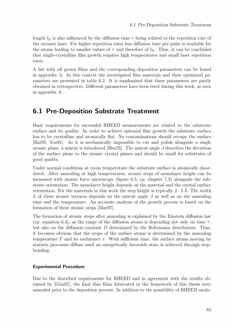
6.1 Pre-Deposition Substrate Treatment
length lD is also influenced by the diffusion time τ being related to the repetition rate ofthe excimer laser. For higher repetition rates less diffusion time per pulse is available forthe atoms leading to smaller values of τ and therefore of lD. Thus, it can be concludedthat single-crystalline film growth requires high temperatures and small laser repetitionrates.
A list with all grown films and the corresponding deposition parameters can be foundin appendix A. In this context the investigated film materials and their optimized pa-rameters are presented in table 6.2. It is emphasized that these parameters are partlyobtained in retrospective. Different parameters have been tried during this work, as seenin appendix A.
6.1 Pre-Deposition Substrate Treatment
Basic requirements for successful RHEED measurements are related to the substratesurface and its quality. In order to achieve epitaxial film growth the substrate surfacehas to be crystalline and atomically flat. No contaminations should occupy the surface[Bar95, Yos95]. As it is mechanically impossible to cut and polish alongside a singleatomic plane, a miscut is introduced [Hen76]. The miscut angle β describes the deviationof the surface plane to the atomic crystal planes and should be small for substrates ofgood quality.
Under normal conditions at room temperature the substrate surface is atomically disor-dered. After annealing at high temperatures, atomic steps of monolayer height can bemeasured with atomic force microscopy (figure 6.5, cp. chapter 7.3) alongside the sub-strate orientation. The monolayer height depends on the material and the crystal surfaceorientation. For the materials in this work the step height is typically 2 – 5 A. The widthL of these atomic terraces depends on the miscut angle β as well as on the annealingtime and the temperature. An accurate analysis of the growth process is based on theformation of these atomic steps [Mae97].
The formation of atomic steps after annealing is explained by the Einstein diffusion law(cp. equation 6.3), as the range of the diffusion atoms is depending not only on time τ ,but also on the diffusion constant D determined by the Boltzmann distribution. Thus,it becomes obvious that the scope of the surface atoms is determined by the annealingtemperature T and its endurance τ . With sufficient time, the surface atoms moving bystatistic processes diffuse until an energetically favorable state is achieved through step-bonding.
Experimental Procedure
Due to the described requirements for RHEED and in agreement with the results ob-tained by [Gun07], the final thin films fabricated in the framework of this thesis wereannealed prior to the deposition process. In addition to the possibility of RHEED analy-
65
6 Thin Film Preparation
Figure 6.5: AFM images of (0001) sapphire substrates: (a) as-supplied (1×1 � m2), (b)annealed at 1000 � C for 1 h (1×1 � m2), and (c) annealed at 1400 � C for 1 h (3×3 � m2).The vertical profile was taken along the line indicated in the image. [Yos95]
sis, this thermal treatment and the subsequent surface characterization with atomic forcemicroscopy provided additional information regarding the source material condition.
Two devices have been used for thermal substrate treatment. Annealing at temperaturesof T < 1000 � C was done in a pipe furnace, whereas for annealing at higher temperaturesa programmable furnace by Agni GmbH was employed. To prevent any surface con-tamination, the single-side polished substrates were enclosed in a aluminum-ceramic case.After annealing, the substrates were characterized with AFM to determine the atomicstep orientation together with the miscut angle. During deposition, the incident electronbeam of the RHEED system was oriented parallel to the atomic steps of the substrates.Although film growth monitor with the incident electron beam oriented perpendicular tothe atomic steps is possible, better monitoring was achieved in parallel settings [Gun07].In substrates with high miscut angles step-bunching is likely to occur [Joy88, Gun07],which can result in three-dimensional island growth. Thus, substrates with high miscutangles can affect the growth mode of the deposited film [Rij04].
In dependence of the miscut angle and the incorporated trivalent ion, the sesquioxidesrequire annealing at 800 – 1200 � C. Surface arrangement of scandia requires higher tem-peratures compared to the one of yttria [Gun07]. Temperatures of 900 � C were used forthe thermal treatment of [111] and [100] Y2O3 substrates. A relatively high miscut ofβ ≥ 0.15 � was observed for composite (Sc, Lu)2O3 substrates. Therefore, lower annealingtemperatures of 700 – 800 � C were used. Sapphire and YAG substrate were annealed at1000 � C, YVO4 substrates were annealed at 800 � C, and LiYF4 substrates were annealed at500 � C. In order to prevent a reaction with oxygen, the thermal treatment of the fluoridesubstrates took place in argon atmosphere. In all cases the annealing time was 1 h.
66
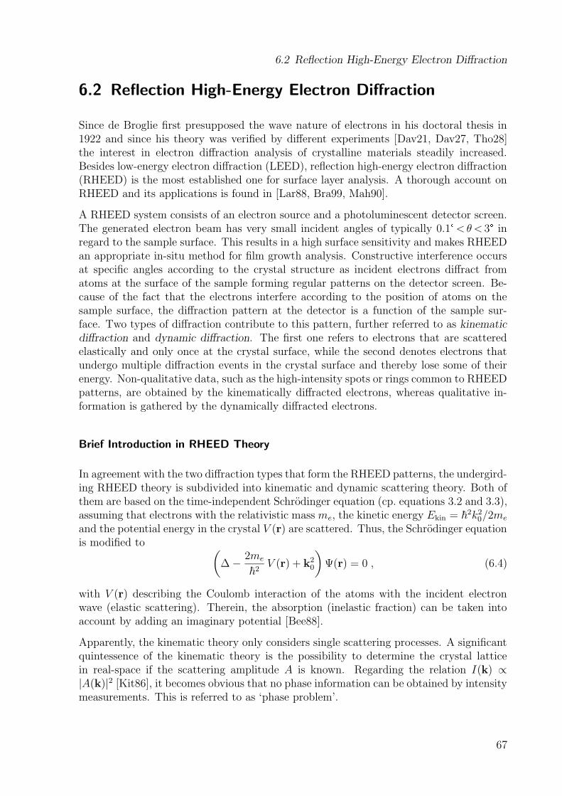
6.2 Reflection High-Energy Electron Diffraction
6.2 Reflection High-Energy Electron Diffraction
Since de Broglie first presupposed the wave nature of electrons in his doctoral thesis in1922 and since his theory was verified by different experiments [Dav21, Dav27, Tho28]the interest in electron diffraction analysis of crystalline materials steadily increased.Besides low-energy electron diffraction (LEED), reflection high-energy electron diffraction(RHEED) is the most established one for surface layer analysis. A thorough account onRHEED and its applications is found in [Lar88, Bra99, Mah90].
A RHEED system consists of an electron source and a photoluminescent detector screen.The generated electron beam has very small incident angles of typically 0.1 � <θ< 3 � inregard to the sample surface. This results in a high surface sensitivity and makes RHEEDan appropriate in-situ method for film growth analysis. Constructive interference occursat specific angles according to the crystal structure as incident electrons diffract fromatoms at the surface of the sample forming regular patterns on the detector screen. Be-cause of the fact that the electrons interfere according to the position of atoms on thesample surface, the diffraction pattern at the detector is a function of the sample sur-face. Two types of diffraction contribute to this pattern, further referred to as kinematic
diffraction and dynamic diffraction. The first one refers to electrons that are scatteredelastically and only once at the crystal surface, while the second denotes electrons thatundergo multiple diffraction events in the crystal surface and thereby lose some of theirenergy. Non-qualitative data, such as the high-intensity spots or rings common to RHEEDpatterns, are obtained by the kinematically diffracted electrons, whereas qualitative in-formation is gathered by the dynamically diffracted electrons.
Brief Introduction in RHEED Theory
In agreement with the two diffraction types that form the RHEED patterns, the undergird-ing RHEED theory is subdivided into kinematic and dynamic scattering theory. Both ofthem are based on the time-independent Schrodinger equation (cp. equations 3.2 and 3.3),assuming that electrons with the relativistic mass me, the kinetic energy Ekin = ~2k20/2me
and the potential energy in the crystal V (r) are scattered. Thus, the Schrodinger equationis modified to
(
∆− 2me
~2V (r) + k20
)
Ψ(r) = 0 , (6.4)
with V (r) describing the Coulomb interaction of the atoms with the incident electronwave (elastic scattering). Therein, the absorption (inelastic fraction) can be taken intoaccount by adding an imaginary potential [Bee88].
Apparently, the kinematic theory only considers single scattering processes. A significantquintessence of the kinematic theory is the possibility to determine the crystal latticein real-space if the scattering amplitude A is known. Regarding the relation I(k) ∝|A(k)|2 [Kit86], it becomes obvious that no phase information can be obtained by intensitymeasurements. This is referred to as ‘phase problem’.
67
6 Thin Film Preparation
Different types of information on the sample are provided by the dynamic theory de-scribing inelastic and multiple scattering events. Intensity of diffraction points is relatedto dynamic scattering. Inelastically scattered electrons that have already penetratedthe surface and subsequently fulfill the Bragg condition yield diffraction patterns calledKikuchi lines [Kik28, Bol88]. Not only are these lines useful for estimating the diffractionconditions. They contain additional information on the surface quality and the crystalorientation of the sample. Narrow Kikuchi lines of distinct intensity suggest high surfacequality, as the electrons are scattered at multiple parallel atomic planes and have the sameangle when escaping the crystal. However, the Kikuchi lines sometimes interfere with thediffraction points, especially while monitoring film growth, and modify the RHEED im-age. It is thus commendable to measure diffraction points in an area with no influence ofKikuchi lines.
In the dynamic theory the Schrodinger equation is solved by approximation. Three solv-ing methods are known in literature [Bra99]: the Bethe-Bloch wave method, the parallel-slicing method, and the multiple-slicing formalism. By applying the periodicity of thecrystal potential with varying boundary conditions, all methods deliver good results thatare strongly related to experimental data. As a detailed and satisfying theoretical de-scription would go beyond the scope of this thesis reference is made to the diversity ofliterature that provides insight into these RHEED fundamentals [Bra99, Lar88].
Geometrical Considerations
f
Figure 6.6: Schematic illustration of (a) theEwald construction and (b) the projection to theparallel surface plane. [Her83]
In order to obtain the crystallographicproperties of the sample surface, an Ewaldsphere is constructed [Her83], indicat-ing the allowed diffraction conditions forkinematically scattered electrons. Thus,knowing the incident electron energy andthe distance between detector and sam-ple, the reciprocal sample lattice can beestimated by a diffraction pattern that isrelated to the constructed Ewald sphere.This is shown schematically in figure 6.6.
Incident high-energy electrons with wavevector k0 that strike the sample surfacewith the grazing angle θ are scatteredand exit with wave vector ki. In thekinematic theory, the scattered electronsare describes by the Laue condition G =ki − k0, with G denoting the recipro-cal lattice vector [Kit86]. An equivalentdescription is given by the Bragg condi-tion4 2dhkl sin θ = nλe. Since the electrons
4 The Bragg diffraction law as well as the Miller indices h, k and l are explained in chapter 7.1
68
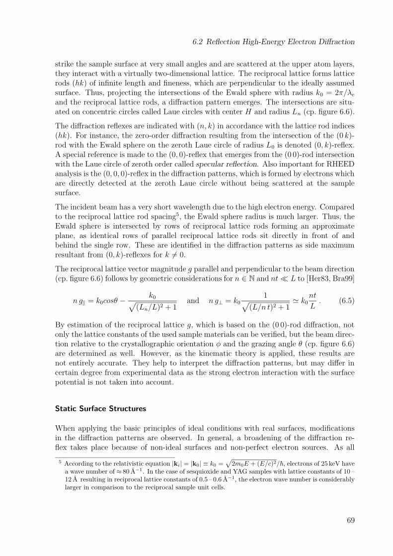
6.2 Reflection High-Energy Electron Diffraction
strike the sample surface at very small angles and are scattered at the upper atom layers,they interact with a virtually two-dimensional lattice. The reciprocal lattice forms latticerods (hk) of infinite length and fineness, which are perpendicular to the ideally assumedsurface. Thus, projecting the intersections of the Ewald sphere with radius k0 = 2π/λeand the reciprocal lattice rods, a diffraction pattern emerges. The intersections are situ-ated on concentric circles called Laue circles with center H and radius Ln (cp. figure 6.6).
The diffraction reflexes are indicated with (n, k) in accordance with the lattice rod indices(hk). For instance, the zero-order diffraction resulting from the intersection of the (0 k)-rod with the Ewald sphere on the zeroth Laue circle of radius L0 is denoted (0, k)-reflex.A special reference is made to the (0, 0)-reflex that emerges from the (0 0)-rod intersectionwith the Laue circle of zeroth order called specular reflection. Also important for RHEEDanalysis is the (0, 0, 0)-reflex in the diffraction patterns, which is formed by electrons whichare directly detected at the zeroth Laue circle without being scattered at the samplesurface.
The incident beam has a very short wavelength due to the high electron energy. Comparedto the reciprocal lattice rod spacing5, the Ewald sphere radius is much larger. Thus, theEwald sphere is intersected by rows of reciprocal lattice rods forming an approximateplane, as identical rows of parallel reciprocal lattice rods sit directly in front of andbehind the single row. These are identified in the diffraction patterns as side maximumresultant from (0, k)-reflexes for k 6= 0.
The reciprocal lattice vector magnitude g parallel and perpendicular to the beam direction(cp. figure 6.6) follows by geometric considerations for n ∈ N and nt¿ L to [Her83, Bra99]
n g‖ = k0cosθ −k0
√
(Ln/L)2 + 1and n g⊥ = k0
1√
(L/n t)2 + 1' k0
nt
L. (6.5)
By estimation of the reciprocal lattice g, which is based on the (0 0)-rod diffraction, notonly the lattice constants of the used sample materials can be verified, but the beam direc-tion relative to the crystallographic orientation φ and the grazing angle θ (cp. figure 6.6)are determined as well. However, as the kinematic theory is applied, these results arenot entirely accurate. They help to interpret the diffraction patterns, but may differ incertain degree from experimental data as the strong electron interaction with the surfacepotential is not taken into account.
Static Surface Structures
When applying the basic principles of ideal conditions with real surfaces, modificationsin the diffraction patterns are observed. In general, a broadening of the diffraction re-flex takes place because of non-ideal surfaces and non-perfect electron sources. As all
5 According to the relativistic equation |ki| = |k0| ≡ k0 =√
2m0E + (E/c)2/~, electrons of 25 keV havea wave number of ≈ 80 A−1. In the case of sesquioxide and YAG samples with lattice constants of 10 –12 A resulting in reciprocal lattice constants of 0.5 – 0.6 A−1, the electron wave number is considerablylarger in comparison to the reciprocal sample unit cells.
69
6 Thin Film Preparation
(a) (b) (c)
Figure 6.7: RHEED images with varying incident electron beam orientation to theatomic steps on the sample surface: (a) YVO4 substrate (parallel), (b) an YVO4
substrate (perpendicular), and (c) a 15 nm thin Eu:(Sc, Lu)2O3 film (parallel).
wave fractions are incoherent, the experimental intensity Iex is algebraically derived fromconvolution of the real sample intensity Is(k) (ideal electron source) with the instrumentresponse function Ti(k) of the electron gun [Hen91]
Iex = Is(k) ∗ Ti(k) . (6.6)
The autocorrelation function φ(r), which describes the probability to find two surfaceatoms at distance r, and the transfer function t(r) are obtained by Fourier transformationF of both components
Is(k) = Fφ(r) and Ti(k) = F t(r) . (6.7)
Apart from this, inelastically scattered electrons cause another broadening. The finiteelectron expansion modifies the diffraction points to ellipses, as the correlated theoreticalmodel (e. g. intersection with lattice rods of infinite fineness) are corrected. Thus, RHEEDdiffraction points often have an elliptic form as shown in figure 6.7 (c) and their degreeof circularity gives evidence to the quality of the sample surface.
When reconsidering the atomic surface steps, the electron beam alignment relative to thesesteps brings forth varying diffraction images in the so-called off-Bragg condition (alsoreferred to as out-of-phase condition). Parallel alignment results in ordinary patternsas seen in figure 6.7 (a), whereas perpendicular alignment leads to a splitting of thediffraction reflexes as observed in figure 6.7 (b). Based on the kinematic theory andthe constraining assumption that electron scattering occurs on the outermost surfaceatoms only, an autocorrelation function for a two-level system is derived. It describes thestepped surface with step height d and surface coverage Θ ∈ [0, 1], the latter being definedas the ratio of occupied to available adsorption sites [Atk87]. With subsequent Fouriertransformation the intensity is given by [Len84, Puk88]
I(k) =[Θ2 + (1−Θ)2 + 2Θ(1−Θ) cos(kzd)
]2πδ(kx) + 2φ′ii(kx) [1− cos(kzd)] . (6.8)
70
6.2 Reflection High-Energy Electron Diffraction
Therein, φ′ii is the Fourier transform of the reduced autocorrelation function betweenatoms of the same level and depends on the step distribution [Coh86]. Thus, the intensityis an overlay of a delta distribution and a broadened distribution around kx = 0. Based onintensity relation, the different cases of surface coverage must be distinguished to interpretthe diffraction reflections correctly.
a) Θ = 0, d = 0: In the case of atomically flat surfaces without two-dimensional islandformations, the delta distribution defines the intensity. Thus, the diffraction pointcan be regarded as delta peak.
b) Θ 6= 0 in-phase: Fulfilling the Bragg condition kzd = 2nπ, all delta distributionsdeliver a RHEED reflex. This is similar to the case with atomically flat surfaces.The steps are not recognized by the electrons.
c) Θ 6= 0 out-of-phase: Fulfilling the off-Bragg condition kzd = (2n + 1)π, the in-tensity is highly sensitive to the surface coverage Θ. The steps are visible in thediffraction pattern, as for kzd values the delta peak and the broadened peak super-impose.
Apparently, the off-Bragg condition is ideally suited to detect surface derangements. Al-though the diffraction peak splitting in the off-Bragg condition (perpendicular incidentbeam) can be used to determine the miscut angle β [Coh86, Puk88], it may disturb thein-situ growth monitoring. Thus, the electron beam was applied in parallel orientationrelative to the atomic steps on the surface, and the miscut was determined by AFM.
71
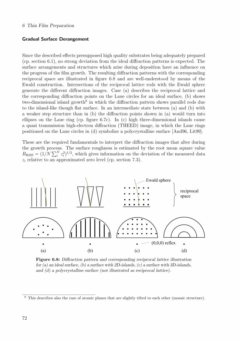
6 Thin Film Preparation
Gradual Surface Derangement
Since the described effects presupposed high quality substrates being adequately prepared(cp. section 6.1), no strong deviation from the ideal diffraction patterns is expected. Thesurface arrangements and structures which arise during deposition have an influence onthe progress of the film growth. The resulting diffraction patterns with the correspondingreciprocal space are illustrated in figure 6.8 and are well-understood by means of theEwald construction. Intersections of the reciprocal lattice rods with the Ewald spheregenerate the different diffraction images. Case (a) describes the reciprocal lattice andthe corresponding diffraction points on the Laue circles for an ideal surface, (b) showstwo-dimensional island growth6 in which the diffraction pattern shows parallel rods dueto the island-like though flat surface. In an intermediate state between (a) and (b) witha weaker step structure than in (b) the diffraction points shown in (a) would turn intoellipses on the Laue ring (cp. figure 6.7c). In (c) high three-dimensional islands causea quasi transmission high-electron diffraction (THEED) image, in which the Laue ringspositioned on the Laue circles in (d) symbolize a polycrystalline surface [And96, Lit99].
These are the required fundamentals to interpret the diffraction images that alter duringthe growth process. The surface roughness is estimated by the root mean square valueRRMS = (1/N
∑Ni z
2i )
1/2, which gives information on the deviation of the measured datazi relative to an approximated zero level (cp. section 7.3).
(a) (b) (c) (d)
Ewald sphere
reciprocalspace
(0,0,0) reflex
Figure 6.8: Diffraction pattern and corresponding reciprocal lattice illustrationfor (a) an ideal surface, (b) a surface with 2D-islands, (c) a surface with 3D-islands,and (d) a polycrystalline surface (not illustrated as reciprocal lattice).
6 This describes also the case of atomic planes that are slightly tilted to each other (mosaic structure).
72
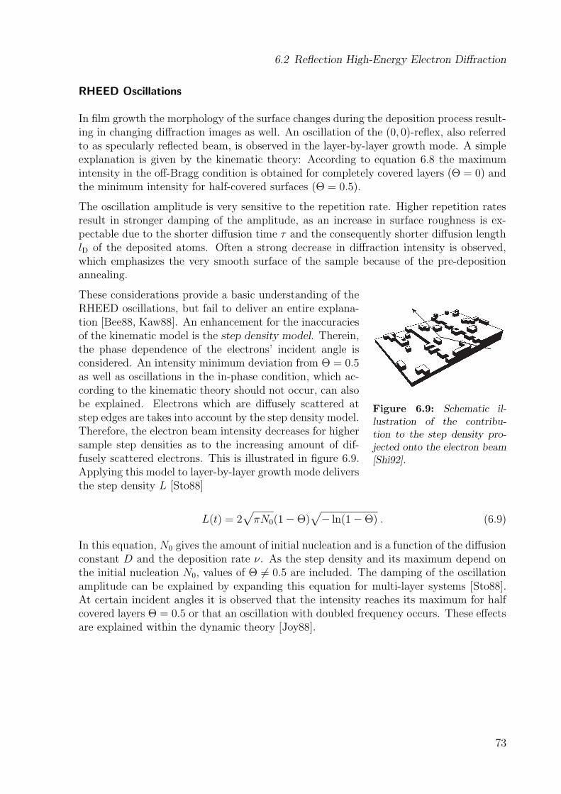
6.2 Reflection High-Energy Electron Diffraction
RHEED Oscillations
In film growth the morphology of the surface changes during the deposition process result-ing in changing diffraction images as well. An oscillation of the (0, 0)-reflex, also referredto as specularly reflected beam, is observed in the layer-by-layer growth mode. A simpleexplanation is given by the kinematic theory: According to equation 6.8 the maximumintensity in the off-Bragg condition is obtained for completely covered layers (Θ = 0) andthe minimum intensity for half-covered surfaces (Θ = 0.5).
The oscillation amplitude is very sensitive to the repetition rate. Higher repetition ratesresult in stronger damping of the amplitude, as an increase in surface roughness is ex-pectable due to the shorter diffusion time τ and the consequently shorter diffusion lengthlD of the deposited atoms. Often a strong decrease in diffraction intensity is observed,which emphasizes the very smooth surface of the sample because of the pre-depositionannealing.
Figure 6.9: Schematic il-lustration of the contribu-tion to the step density pro-jected onto the electron beam[Shi92].
These considerations provide a basic understanding of theRHEED oscillations, but fail to deliver an entire explana-tion [Bee88, Kaw88]. An enhancement for the inaccuraciesof the kinematic model is the step density model. Therein,the phase dependence of the electrons’ incident angle isconsidered. An intensity minimum deviation from Θ = 0.5as well as oscillations in the in-phase condition, which ac-cording to the kinematic theory should not occur, can alsobe explained. Electrons which are diffusely scattered atstep edges are takes into account by the step density model.Therefore, the electron beam intensity decreases for highersample step densities as to the increasing amount of dif-fusely scattered electrons. This is illustrated in figure 6.9.Applying this model to layer-by-layer growth mode deliversthe step density L [Sto88]
L(t) = 2√
πN0(1−Θ)√
− ln(1−Θ) . (6.9)
In this equation, N0 gives the amount of initial nucleation and is a function of the diffusionconstant D and the deposition rate ν. As the step density and its maximum depend onthe initial nucleation N0, values of Θ 6= 0.5 are included. The damping of the oscillationamplitude can be explained by expanding this equation for multi-layer systems [Sto88].At certain incident angles it is observed that the intensity reaches its maximum for halfcovered layers Θ = 0.5 or that an oscillation with doubled frequency occurs. These effectsare explained within the dynamic theory [Joy88].
73
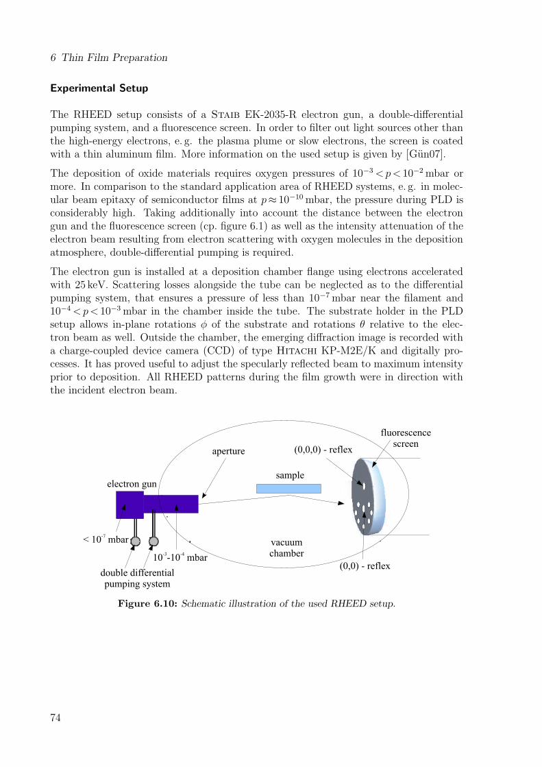
6 Thin Film Preparation
Experimental Setup
The RHEED setup consists of a Staib EK-2035-R electron gun, a double-differentialpumping system, and a fluorescence screen. In order to filter out light sources other thanthe high-energy electrons, e. g. the plasma plume or slow electrons, the screen is coatedwith a thin aluminum film. More information on the used setup is given by [Gun07].
The deposition of oxide materials requires oxygen pressures of 10−3<p< 10−2mbar ormore. In comparison to the standard application area of RHEED systems, e. g. in molec-ular beam epitaxy of semiconductor films at p≈ 10−10mbar, the pressure during PLD isconsiderably high. Taking additionally into account the distance between the electrongun and the fluorescence screen (cp. figure 6.1) as well as the intensity attenuation of theelectron beam resulting from electron scattering with oxygen molecules in the depositionatmosphere, double-differential pumping is required.
The electron gun is installed at a deposition chamber flange using electrons acceleratedwith 25 keV. Scattering losses alongside the tube can be neglected as to the differentialpumping system, that ensures a pressure of less than 10−7mbar near the filament and10−4<p< 10−3mbar in the chamber inside the tube. The substrate holder in the PLDsetup allows in-plane rotations φ of the substrate and rotations θ relative to the elec-tron beam as well. Outside the chamber, the emerging diffraction image is recorded witha charge-coupled device camera (CCD) of type Hitachi KP-M2E/K and digitally pro-cesses. It has proved useful to adjust the specularly reflected beam to maximum intensityprior to deposition. All RHEED patterns during the film growth were in direction withthe incident electron beam.
electron gunsample
vacuumchamber
< 10 mbar-7
double differentialpumping system
(0,0,0) - reflex
(0,0) - reflex
fluorescencescreen
aperture
10 -1 mbar-3
0-4
Figure 6.10: Schematic illustration of the used RHEED setup.
74
7 Analytical Techniques
A variety of measuring methods is required to characterize thin crystalline films regard-ing their structural and optical properties. In this chapter the analytical methods andexperimental setups which have been employed throughout this work are described. Thecharacterization process of the films can be subdivided into two parts, namely
i) in-situ techniques: The characterization methods in this category include reflec-tometry (film thickness) and RHEED (surface structure and growth mode analysis;cp. chapter 6.2), both applied during the pulsed laser deposition process of the film.
ii) ex-situ techniques: Included therein are analytical tools for examining the struc-ture of the films, such as X-ray diffraction (crystallinity), ellipsometry (refractiveindex), and atomic force microscopy (surface morphology). The optical propertiesof the rare-earth-doped films are examined by fluorescence and excitation measure-ments (including VUV excitation measurements) as well as lifetime measurements.
7.1 X-Ray Diffraction
A non-destructive technique for examining the crystalline structure of the sample materialcan be found in the X-ray diffraction (XRD) method. It is based on the analysis of theangular intensity distribution of a monochromatic X-ray beam of wavelength λ that isreflected from the sample.
Any given crystal lattice, e. g. cubic, rhombic et cetera, consists of a regular three-dimensional spatial distribution of periodically arranged atoms which form a series ofparallel planes separated from each other by a distance d. X-rays propagating througha crystal show a detectable pattern by the varying intensity of the scattered rays. Thisderives from the interference of the individual X-ray waves scattered at each atom, i. e.at the electrons of the inner atomic shells (Thomson scattering). Two opposite cases canbe distinguished.
1. Amorphous material: The atoms are randomly arranged in the material, thus thescattered X-rays are incoherent and the resulting intensity is proportional to thetotal number of scattering centers N.
75
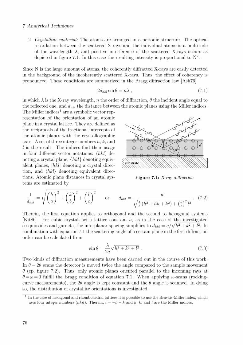
7 Analytical Techniques
2. Crystalline material: The atoms are arranged in a periodic structure. The opticalretardation between the scattered X-rays and the individual atoms is a multitudeof the wavelength λ, and positive interference of the scattered X-rays occurs asdepicted in figure 7.1. In this case the resulting intensity is proportional to N2.
Since N is the large amount of atoms, the coherently diffracted X-rays are easily detectedin the background of the incoherently scattered X-rays. Thus, the effect of coherency ispronounced. These conditions are summarized in the Bragg diffraction law [Ash76]
2dhkl sin θ = nλ , (7.1)
in which λ is the X-ray wavelength, n the order of diffraction, θ the incident angle equal tothe reflected one, and dhkl the distance between the atomic planes using the Miller indices.
q
q
2q
d d
substrate
Figure 7.1: X-ray diffraction
The Miller indices1 are a symbolic vector rep-resentation of the orientation of an atomicplane in a crystal lattice. They are defined asthe reciprocals of the fractional intercepts ofthe atomic planes with the crystallographicaxes. A set of three integer numbers h, k, andl is the result. The indices find their usagein four different vector notations: (hkl) de-noting a crystal plane, {hkl} denoting equiv-alent planes, [hkl] denoting a crystal direc-tion, and 〈hkl〉 denoting equivalent direc-tions. Atomic plane distances in crystal sys-tems are estimated by
1
dhkl=
√(h
a
)2
+
(k
b
)2
+
(l
c
)2
or dhkl =a
√
43(h2 + hk + k2) +
(ac
)2l2. (7.2)
Therein, the first equation applies to orthogonal and the second to hexagonal systems[Kit86]. For cubic crystals with lattice constant a, as in the case of the investigatedsesquioxides and garnets, the interplanar spacing simplifies to dhkl = a/
√h2 + k2 + l2. In
combination with equation 7.1 the scattering angle of a certain plane in the first diffractionorder can be calculated from
sin θ =λ
2a
√h2 + k2 + l2 . (7.3)
Two kinds of diffraction measurements have been carried out in the course of this work.In θ− 2θ scans the detector is moved twice the angle compared to the sample movementθ (cp. figure 7.2). Thus, only atomic planes oriented parallel to the incoming rays atθ=ω=0 fulfill the Bragg condition of equation 7.1. When applying ω-scans (rocking-curve measurements), the 2θ angle is kept constant and the θ angle is scanned. In doingso, the distribution of crystallite orientations is investigated.
1 In the case of hexagonal and rhombohedral lattices it is possible to use the Bravais-Miller index, whichuses four integer numbers (hkil). Therein, i = −h− k and h, k, and l are the Miller indices.
76
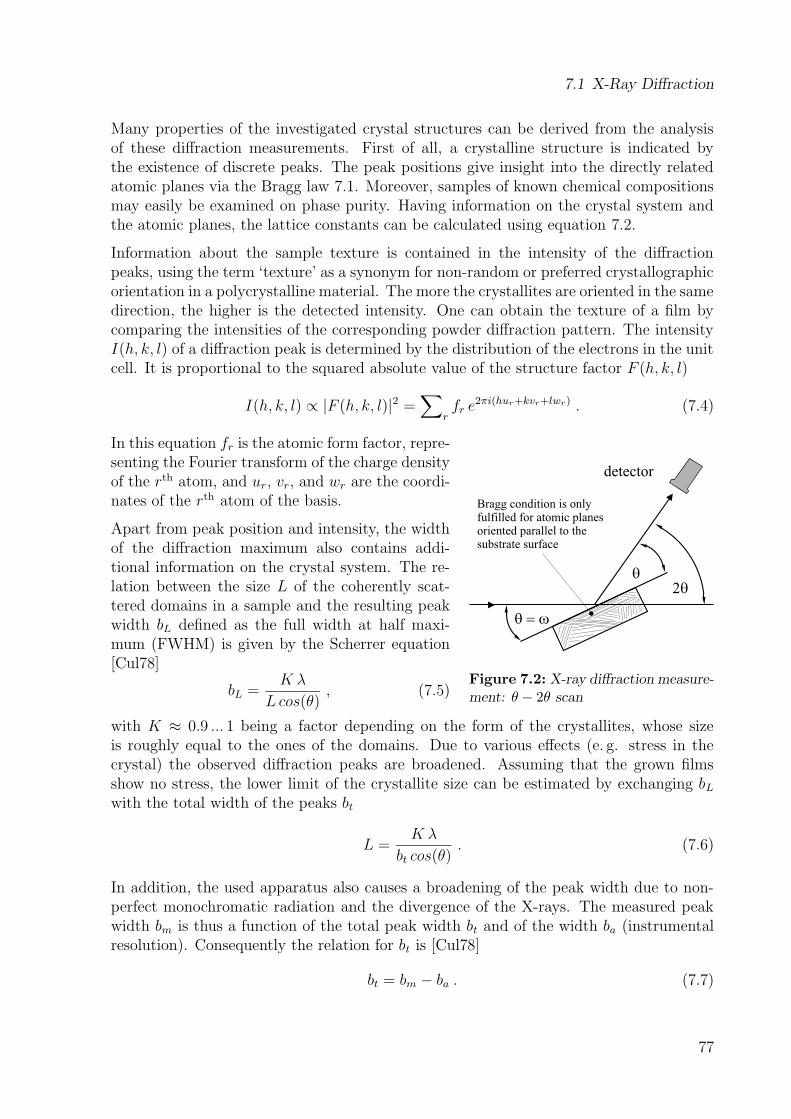
7.1 X-Ray Diffraction
Many properties of the investigated crystal structures can be derived from the analysisof these diffraction measurements. First of all, a crystalline structure is indicated bythe existence of discrete peaks. The peak positions give insight into the directly relatedatomic planes via the Bragg law 7.1. Moreover, samples of known chemical compositionsmay easily be examined on phase purity. Having information on the crystal system andthe atomic planes, the lattice constants can be calculated using equation 7.2.
Information about the sample texture is contained in the intensity of the diffractionpeaks, using the term ‘texture’ as a synonym for non-random or preferred crystallographicorientation in a polycrystalline material. The more the crystallites are oriented in the samedirection, the higher is the detected intensity. One can obtain the texture of a film bycomparing the intensities of the corresponding powder diffraction pattern. The intensityI(h, k, l) of a diffraction peak is determined by the distribution of the electrons in the unitcell. It is proportional to the squared absolute value of the structure factor F (h, k, l)
I(h, k, l) ∝ |F (h, k, l)|2 =∑
rfr e
2πi(hur+kvr+lwr) . (7.4)
q = w
2q
q
detector
Bragg condition is onlyatomic planesfulfilled for
oriented parallel to thesubstrate surface
Figure 7.2: X-ray diffraction measure-ment: θ − 2θ scan
In this equation fr is the atomic form factor, repre-senting the Fourier transform of the charge densityof the rth atom, and ur, vr, and wr are the coordi-nates of the rth atom of the basis.
Apart from peak position and intensity, the widthof the diffraction maximum also contains addi-tional information on the crystal system. The re-lation between the size L of the coherently scat-tered domains in a sample and the resulting peakwidth bL defined as the full width at half maxi-mum (FWHM) is given by the Scherrer equation[Cul78]
bL =K λ
L cos(θ), (7.5)
with K ≈ 0.9 ... 1 being a factor depending on the form of the crystallites, whose sizeis roughly equal to the ones of the domains. Due to various effects (e. g. stress in thecrystal) the observed diffraction peaks are broadened. Assuming that the grown filmsshow no stress, the lower limit of the crystallite size can be estimated by exchanging bLwith the total width of the peaks bt
L =K λ
bt cos(θ). (7.6)
In addition, the used apparatus also causes a broadening of the peak width due to non-perfect monochromatic radiation and the divergence of the X-rays. The measured peakwidth bm is thus a function of the total peak width bt and of the width ba (instrumentalresolution). Consequently the relation for bt is [Cul78]
bt = bm − ba . (7.7)
77
7 Analytical Techniques
Assuming that both the diffraction peaks as well as the instrumental broadening have aGaussian profile, the total peak widths are determined by [Bro95]
bt =√
b2m − b2a . (7.8)
Though the diffraction lines actually have a form that is described by the Pseudo-Voigtfunction, which is a mixture of a Gaussian and Lorentzian profile, the line profiles do notdeviate much from the Gaussian form and therefore justify the use of this approximation.
The crystallite size of a sample can now be estimated using these two corrections incombination with equation 7.6. For example, when setting K = 1, diffraction peaksresulting from X-ray wavelengths of λCu−Kα1
= 1.5406 A deliver the equation
L(nm) =8.827
b(deg)t cos(θ)
. (7.9)
Although the X-ray measurement technique is mainly used to characterize samples inpowder form, it can also be employed for thin film characterization taking into accounttwo limitations:
1. The films need to have a minimum thickness, which grants a certain amount ofatomic planes available for diffraction. It is necessary that the intensity of thediffracted X-rays is high enough to be detected.
2. If the film under investigation has no atomic planes parallel to the sample surface,no signal is detected, not even in the case of good crystal quality. It could also bepossible that such films are mistaken as amorphous. This worst case is related tofilms of one predominant crystallite growth direction, especially to single-crystallinesamples.
Experimental Setup
As no in-house systems were available, the X-ray diffraction measurements were carriedout at the Technische Universitat Hamburg-Harburg using a powder X-ray diffractionmachine with parallel beam optics of type D8 Advance by the company Bruker Axs.
A copper cathode with monochromatic X-ray radiation of wavelength λCu−Kα1=1.5406 A
is used as X-ray source. Behind the cathode, a Gobel-mirror generates a parallel beamof rays. The samples are arranged on perspex holders and mounted with plasticine. Ablock of parallel metal plates called Soller-block is located in front of the detector, itsgeometry defining a tolerance angle. Only rays with a divergence angle smaller than thetolerance angle can pass the Soller-block. Thereby, the fluorescence excited by the X-rayradiation is effectively suppressed without the usage of additional filters. The experimentalparameters used in the measurements are 40 kV and 40mA for the acceleration radiationand the anode current, respectively. The instrumental resolution depends on the selectedslit set and is estimated to be ba = 0.084 � for regular scans.
78
7.1 X-Ray Diffraction
Additional measurements were performed at the Fachhochschule Wedel using a SiemensKristalloflex 810 diffractometer, which is also supplied with a copper X-ray sourceoperating at 40 kV and 20mA. This setup provides non-monochromatic X-ray radiationwith a removable Ni-screen to filter out the λCu−Kβ
emission. Therefore multiple Cu-lines are present in the diffraction spectra: Kα1, Kα2, and a residue of the Kβ line. TheX-ray radiation occurs at wavelengths of λCu−Kα1
=1.5406 A , λCu−Kα2=1.5444 A , and
λCu−Kβ=1.3922 A. However, the Cu-Kα1 and Cu-Kα2 lines are not always resolved because
of the reflection broadening.
Overview measurements were performed with the slit set that provided a nominal reso-lution of 0.15 � . High resolution θ − 2θ scans, which were used in order to determine thediffraction peak width, and also rocking-curve measurements were done using slit setswith the nominal resolution of 0.05 � or 0.018 � . An instrumental resolution ba of 0.04 �was determined for the high resolution scans. As the diffraction peaks of lattice matchedquasi-homoepitaxial substrate–film materials are closely united in the spectra, it some-times proved useful to remove the Ni-filter and perform high resolution scans using theCu-Kβ line for analysis.
79
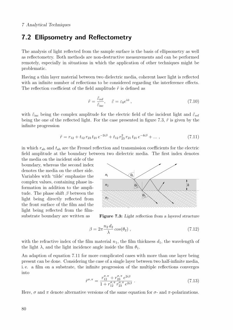
7 Analytical Techniques
7.2 Ellipsometry and Reflectometry
The analysis of light reflected from the sample surface is the basis of ellipsometry as wellas reflectometry. Both methods are non-destructive measurements and can be performedremotely, especially in situations in which the application of other techniques might beproblematic.
Having a thin layer material between two dielectric media, coherent laser light is reflectedwith an infinite number of reflections to be considered regarding the interference effects.The reflection coefficient of the field amplitude r is defined as
r =εrefεinc
, ε = ε0eiφ , (7.10)
with εinc being the complex amplitude for the electric field of the incident light and εrefbeing the one of the reflected light. For the case presented in figure 7.3, r is given by theinfinite progression
r = r12 + t12 r23 t21 e−2iβ + t12 r
223 r21 t21 e
−4iβ + ... , (7.11)
in which rab and tab are the Fresnel reflection and transmission coefficients for the electricfield amplitude at the boundary between two dielectric media. The first index denotes
n1
n2
n3
q1
q2
q3
h
Figure 7.3: Light reflection from a layered structure
the media on the incident side of theboundary, whereas the second indexdenotes the media on the other side.Variables with ‘tilde’ emphasize thecomplex values, containing phase in-formation in addition to the ampli-tude. The phase shift β between thelight being directly reflected fromthe front surface of the film and thelight being reflected from the film-substrate boundary are written as
β = 2πn2 d2λ
cos(θ2) , (7.12)
with the refractive index of the film material n1, the film thickness d1, the wavelength ofthe light λ, and the light incidence angle inside the film θ1.
An adaption of equation 7.11 for more complicated cases with more than one layer beingpresent can be done. Considering the case of a single layer between two half-infinite media,i. e. a film on a substrate, the infinite progression of the multiple reflections convergesinto
rσ, π =rσ, π12 + rσ, π23 e2iβ
1 + rσ, π12 rσ, π23 e2iβ. (7.13)
Here, σ and π denote alternative versions of the same equation for σ- and π-polarizations.
80
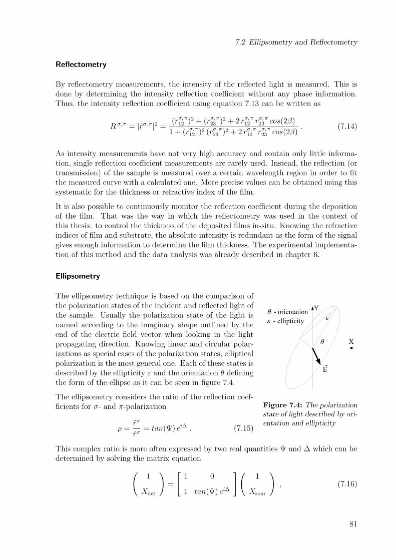
7.2 Ellipsometry and Reflectometry
Reflectometry
By reflectometry measurements, the intensity of the reflected light is measured. This isdone by determining the intensity reflection coefficient without any phase information.Thus, the intensity reflection coefficient using equation 7.13 can be written as
R σ, π = |rσ, π|2 = (rσ, π12 )2 + (rσ, π23 )2 + 2 rσ, π12 rσ, π23 cos(2β)
1 + (rσ, π12 )2 (rσ, π23 )2 + 2 rσ, π12 rσ, π23 cos(2β). (7.14)
As intensity measurements have not very high accuracy and contain only little informa-tion, single reflection coefficient measurements are rarely used. Instead, the reflection (ortransmission) of the sample is measured over a certain wavelength region in order to fitthe measured curve with a calculated one. More precise values can be obtained using thissystematic for the thickness or refractive index of the film.
It is also possible to continuously monitor the reflection coefficient during the depositionof the film. That was the way in which the reflectometry was used in the context ofthis thesis: to control the thickness of the deposited films in-situ. Knowing the refractiveindices of film and substrate, the absolute intensity is redundant as the form of the signalgives enough information to determine the film thickness. The experimental implementa-tion of this method and the data analysis was already described in chapter 6.
Ellipsometry
Figure 7.4: The polarizationstate of light described by ori-entation and ellipticity
The ellipsometry technique is based on the comparison ofthe polarization states of the incident and reflected light ofthe sample. Usually the polarization state of the light isnamed according to the imaginary shape outlined by theend of the electric field vector when looking in the lightpropagating direction. Knowing linear and circular polar-izations as special cases of the polarization states, ellipticalpolarization is the most general one. Each of these states isdescribed by the ellipticity ε and the orientation θ definingthe form of the ellipse as it can be seen in figure 7.4.
The ellipsometry considers the ratio of the reflection coef-ficients for σ- and π-polarization
ρ =rπ
rσ= tan(Ψ) ei∆ . (7.15)
This complex ratio is more often expressed by two real quantities Ψ and ∆ which can bedetermined by solving the matrix equation
(1
Xdet
)
=
[1 0
1 tan(Ψ) ei∆
](1
Xsour
)
, (7.16)
81
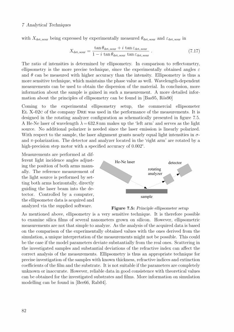
7 Analytical Techniques
with Xdet, sour being expressed by experimentally measured θdet, sour and εdet, sour in
Xdet, sour =tan θdet, sour + i tan εdet, sour1− i tan θdet, sour tan εdet, sour
. (7.17)
The ratio of intensities is determined by ellipsometry. In comparison to reflectometry,ellipsometry is the more precise technique, since the experimentally obtained angles εand θ can be measured with higher accuracy than the intensity. Ellipsometry is thus amore sensitive technique, which maintains the phase value as well. Wavelength-dependentmeasurements can be used to obtain the dispersion of the material. In conclusion, moreinformation about the sample is gained in such a measurement. A more detailed infor-mation about the principles of ellipsometry can be found in [Bas95, Ros90]
Coming to the experimental ellipsometry setup, the commercial ellipsometerEl X-02c of the company Dre was used in the performance of the measurements. It isdesigned in the rotating analyzer configuration as schematically presented in figure 7.5.A He-Ne laser of wavelength λ=632.8 nm makes up the ‘left arm’ and serves as the lightsource. No additional polarizer is needed since the laser emission is linearly polarized.With respect to the sample, the laser alignment grants nearly equal light intensities in σ-and π-polarization. The detector and analyzer located in the ‘right arm’ are rotated by ahigh-precision step motor with a specified accuracy of 0.002 � .
Figure 7.5: Principle ellipsometer setup
Measurements are performed at dif-ferent light incidence angles adjust-ing the position of both arms manu-ally. The reference measurement ofthe light source is performed by set-ting both arms horizontally, directlyguiding the laser beam into the de-tector. Controlled by a computer,the ellipsometer data is acquired andanalyzed via the supplied software.
As mentioned above, ellipsometry is a very sensitive technique. It is therefore possibleto examine silica films of several nanometers grown on silicon. However, ellipsometricmeasurements are not that simple to analyze. As the analysis of the acquired data is basedon the comparison of the experimentally obtained values with the ones derived from thesimulation, a unique interpretation of the measurements might not be possible. This couldbe the case if the model parameters deviate substantially from the real ones. Scattering inthe investigated samples and substantial deviations of the refractive index can affect thecorrect analysis of the measurements. Ellipsometry is thus an appropriate technique forprecise investigation of the samples with known thickness, refractive indices and extinctioncoefficients of the film and the substrate. It is not suitable if the parameters are completelyunknown or inaccurate. However, reliable data in good consistence with theoretical valuescan be obtained for the investigated substrates and films. More information on simulationmodelling can be found in [Ber66, Rab04].
82
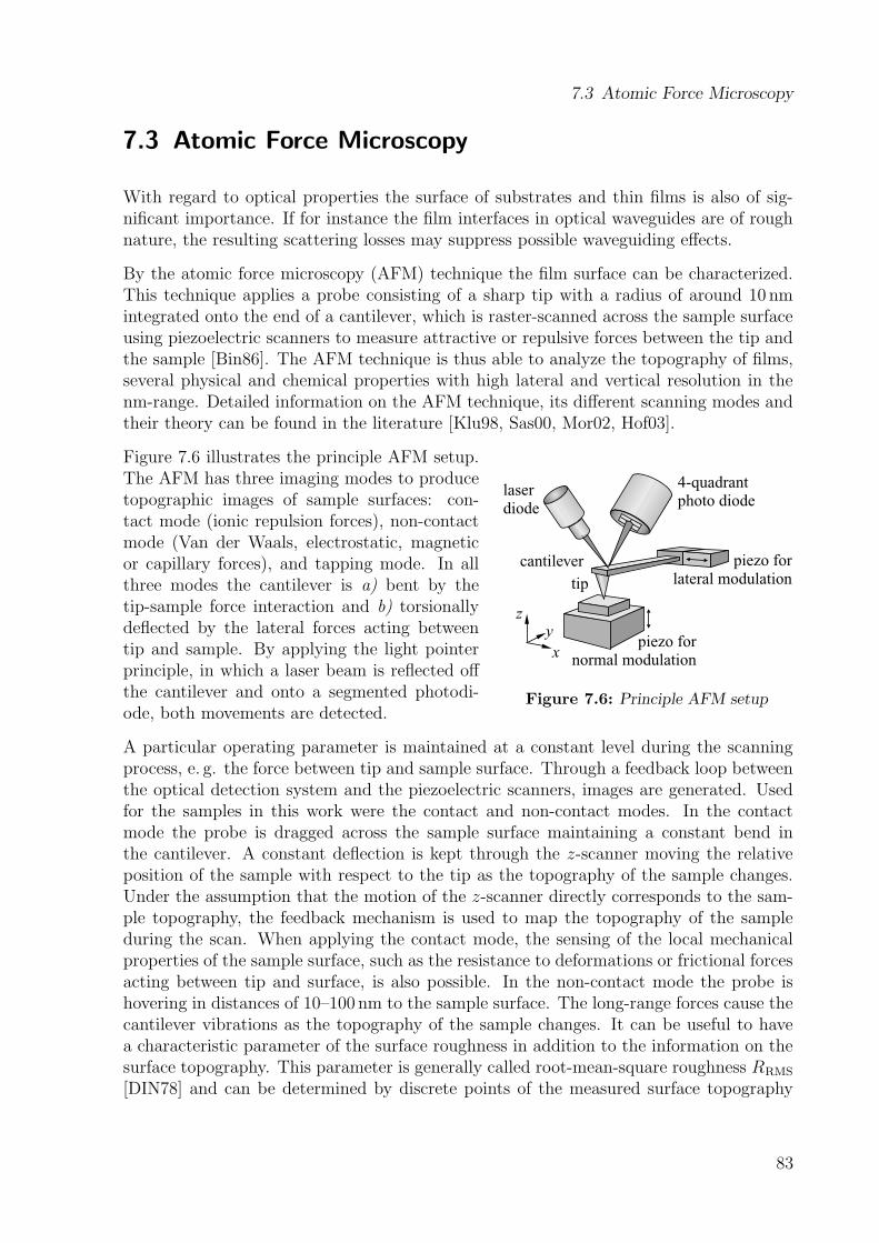
7.3 Atomic Force Microscopy
7.3 Atomic Force Microscopy
With regard to optical properties the surface of substrates and thin films is also of sig-nificant importance. If for instance the film interfaces in optical waveguides are of roughnature, the resulting scattering losses may suppress possible waveguiding effects.
By the atomic force microscopy (AFM) technique the film surface can be characterized.This technique applies a probe consisting of a sharp tip with a radius of around 10 nmintegrated onto the end of a cantilever, which is raster-scanned across the sample surfaceusing piezoelectric scanners to measure attractive or repulsive forces between the tip andthe sample [Bin86]. The AFM technique is thus able to analyze the topography of films,several physical and chemical properties with high lateral and vertical resolution in thenm-range. Detailed information on the AFM technique, its different scanning modes andtheir theory can be found in the literature [Klu98, Sas00, Mor02, Hof03].
xy
z
laserdiode
cantilevertip
4-quadrantphoto diode
piezo forlateral modulation
piezo fornormal modulation
Figure 7.6: Principle AFM setup
Figure 7.6 illustrates the principle AFM setup.The AFM has three imaging modes to producetopographic images of sample surfaces: con-tact mode (ionic repulsion forces), non-contactmode (Van der Waals, electrostatic, magneticor capillary forces), and tapping mode. In allthree modes the cantilever is a) bent by thetip-sample force interaction and b) torsionallydeflected by the lateral forces acting betweentip and sample. By applying the light pointerprinciple, in which a laser beam is reflected offthe cantilever and onto a segmented photodi-ode, both movements are detected.
A particular operating parameter is maintained at a constant level during the scanningprocess, e. g. the force between tip and sample surface. Through a feedback loop betweenthe optical detection system and the piezoelectric scanners, images are generated. Usedfor the samples in this work were the contact and non-contact modes. In the contactmode the probe is dragged across the sample surface maintaining a constant bend inthe cantilever. A constant deflection is kept through the z-scanner moving the relativeposition of the sample with respect to the tip as the topography of the sample changes.Under the assumption that the motion of the z-scanner directly corresponds to the sam-ple topography, the feedback mechanism is used to map the topography of the sampleduring the scan. When applying the contact mode, the sensing of the local mechanicalproperties of the sample surface, such as the resistance to deformations or frictional forcesacting between tip and surface, is also possible. In the non-contact mode the probe ishovering in distances of 10–100 nm to the sample surface. The long-range forces cause thecantilever vibrations as the topography of the sample changes. It can be useful to havea characteristic parameter of the surface roughness in addition to the information on thesurface topography. This parameter is generally called root-mean-square roughness RRMS
[DIN78] and can be determined by discrete points of the measured surface topography
83
7 Analytical Techniques
z(xk, yl). It can be written using the number of data points in x- and y-direction Nx andNy, which are identified by the different indices k and l.
RRMS :=
√√√√ 1
NxNy
Nx∑
k=1
Ny∑
l=1
|z(xk, yl)− z|2 (7.18)
The value z describes a levelled plane with the smallest deviations from the data points(least square fit) [Bra92].
Hard crystalline films, which allow high scanning rates and very sensitive regulation of thetip-surface distance, recommend the contact mode. However, for thin-film layers with flatstructures in the atomic scale the non-contact mode leads to better results [Sas00, Gun07].
7.4 Optical Spectroscopy
Employing optical techniques enables the analysis of local structure modifications, whichare undetectable with methods based on X-ray diffraction. In the course of this workemission and excitation spectroscopy as well as lifetime measurements were carried outfor thin film characterization. The following sections will give an introduction to theemployed techniques and the experimental setups.
Absorption spectra of the europium probe ion could not be obtained due to the consid-erably small film thickness. Absorption cross-sections for interconfigurational transitionsare typically in the range of σa ≈ 10−21 cm2. As the produced films have dopant concen-trations of a few atomic percents, the density of the optically active ions is approximately10 21 cm−3. This results in an absorption length of some millimeters. Therefore, it is not bepossible to detect any absorption of the film with thicknesses in the range of 10 – 500 nm.Moreover, as the substrate is five orders of magnitude thicker than the grown films, itmay heavily influence and overlie any film absorption. Impurities in the substrate, evenof minimum size, would be sufficient to dominate the absorption measurements.
Due to these reasons no absolute absorption cross-sections could be determined, andconsequently, it was not possible to obtain absolute emission cross-sections by using thereciprocity method as well. Therefore, all the spectra measured in this work only showthe spectral photon flux in units of the utilized detector’s counting rate.
84
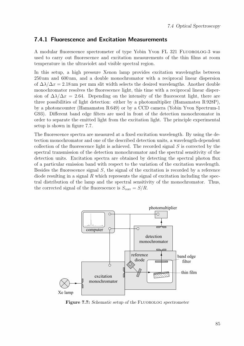
7.4 Optical Spectroscopy
7.4.1 Fluorescence and Excitation Measurements
A modular fluorescence spectrometer of type Yobin Yvon FL 321 Fluorolog-3 wasused to carry out fluorescence and excitation measurements of the thin films at roomtemperature in the ultraviolet and visible spectral region.
In this setup, a high pressure Xenon lamp provides excitation wavelengths between250 nm and 600 nm, and a double monochromator with a reciprocal linear dispersionof ∆λ/∆x = 2.18 nm per mm slit width selects the desired wavelengths. Another doublemonochromator resolves the fluorescence light, this time with a reciprocal linear disper-sion of ∆λ/∆x = 2.64. Depending on the intensity of the fluorescent light, there arethree possibilities of light detection: either by a photomultiplier (Hamamatsu R928P),by a photoncounter (Hamamatsu R649) or by a CCD camera (Yobin Yvon Spectrum-1G93). Different band edge filters are used in front of the detection monochromator inorder to separate the emitted light from the excitation light. The principle experimentalsetup is shown in figure 7.7.
The fluorescence spectra are measured at a fixed excitation wavelength. By using the de-tection monochromator and one of the described detection units, a wavelength-dependentcollection of the fluorescence light is achieved. The recorded signal S is corrected by thespectral transmission of the detection monochromator and the spectral sensitivity of thedetection units. Excitation spectra are obtained by detecting the spectral photon fluxof a particular emission band with respect to the variation of the excitation wavelength.Besides the fluorescence signal S, the signal of the excitation is recorded by a referencediode resulting in a signal R which represents the signal of excitation including the spec-tral distribution of the lamp and the spectral sensitivity of the monochromator. Thus,the corrected signal of the fluorescence is Scorr = S/R.
computer
Xe lamp
excitationmonochromator
detectionmonochromator
referencediode
band edgefilter
thin film
photomultiplier
Figure 7.7: Schematic setup of the Fluorolog spectrometer
85
7 Analytical Techniques
7.4.2 Lifetime Measurements
An excited state i of an optically active ion in a bulk crystal has the lifetime
τV (i) =1
kV (i), (7.19)
with kV (i) denoting the entire transition probability of all radiative and non-radiativetransitions from state i into various destination states. Due to point defects and especiallysurface effects the lifetime in thin films can be reduced according to
τF (i) =1
kV (i) +∑
j kQj (i)
. (7.20)
Therein, kQj (i) is the transition probability from the excited state i due to an additionaldecay channel j, which does not exist in the bulk crystal. A lengthening of the fluorescencelifetime may occur in thin films whose thickness is smaller than the wavelength of thefluorescence light. In this case, the refractive index nf of the film is influenced by therefractive indices of the neighboring media (nf → neff). Consequently, the lifetime of anelectric dipole transition meets the following proportionality [Mel99]:
τ ∼ 1
f
λ2
n9(n2 + 2)2
. (7.21)
In this equation, f denotes the oscillator strength of the transition, whereas the secondterm is referred to as Lorentz correction. This term describes the increase of lifetime fordecreasing refractive indices. Therefore, ultra-thin films surrounded by lower refractingmaterials, such as air, have a higher fluorescence lifetime in comparison to bulk material.
Experimental Setup
Lifetime measurements of thin films at room temperature were carried out at the Instituteof Physical and Theoretical Chemistry, University of Tubingen2, employing a fluorescencespectrophotometer of type Varian Cary Eclipse. The setup is very similar to the oneused for fluorescence and excitation measurements (cp. figure 7.7). Instead of a cw-lampa Xenon flashlamp (≈ 1ms FWHM) serves as excitation source here.
In order to prevent an interference with the decaying flash lamp pulse, the lifetime mea-surements were performed using a delay time of 0.4ms. A gate time of 0.01ms and atotal decay time of 6ms were used. The Eu3+ lifetimes are measured by excitation intothe charge transfer band and detection of the hypersensitive 5D0→ 7F2 transition. Onlyfor aluminum garnet films the stronger 5D0→ 7F1 transition is used.
2The measurements were performed by Dr. Sebastian Bar and Dr. Dmitry Khoptyar.
86
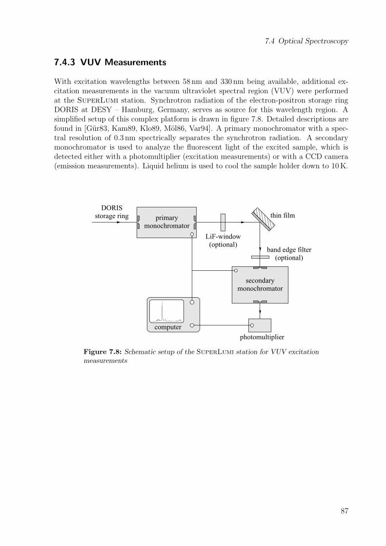
7.4 Optical Spectroscopy
7.4.3 VUV Measurements
With excitation wavelengths between 58 nm and 330 nm being available, additional ex-citation measurements in the vacuum ultraviolet spectral region (VUV) were performedat the SuperLumi station. Synchrotron radiation of the electron-positron storage ringDORIS at DESY – Hamburg, Germany, serves as source for this wavelength region. Asimplified setup of this complex platform is drawn in figure 7.8. Detailed descriptions arefound in [Gur83, Kam89, Klo89, Mol86, Var94]. A primary monochromator with a spec-tral resolution of 0.3 nm spectrically separates the synchrotron radiation. A secondarymonochromator is used to analyze the fluorescent light of the excited sample, which isdetected either with a photomultiplier (excitation measurements) or with a CCD camera(emission measurements). Liquid helium is used to cool the sample holder down to 10K.
computer
DORISstorage ring primary
monochromator
thin film
LiF-window(optional)
band edge filter(optional)
secondarymonochromator
photomultiplier
Figure 7.8: Schematic setup of the SuperLumi station for VUV excitationmeasurements
87

7 Analytical Techniques
88
8 Characterization of
Heteroepitaxial Thin Films
This chapter deals with the characterization of lattice matched heteroepitaxial thin filmsystems. In accordance with the possibilities of lattice matching presented in section 5.2the different lattices of substrate and film material are combined in non-integer multiples(sections 8.1 and 8.2) or integer multiples (section 8.3) of the lattice constants. In addition,some measuring characteristics which are also valid in chapter 9 are introduced in thischapter.
8.1 Composite Sesquioxide Films on Sapphire
Burmester and Bar investigated yttria layers on alumina substrates with a lattice mis-match of 4.73% [Bur02, Bar04]. An approach for a lattice mismatch reduction has beendone by Rabisch with a mixture of scandia and lutetia (Sc0.54Lu0.46)2O3 as layer material[Rab04]. These thin films were grown using the EBV technique. However, different va-por pressure coefficients of scandia and lutetia caused a composition shift of the grown‘lattice matched’ films. Consisting of (Sc0.81Lu0.19)2O3, the films had a lattice constant ofa = 9.948 A with a lattice mismatch of -1.51% to the substrate. A major drawback ofthe EBV technique is that the stoichiometrical transfer depends on the boiling points andvapor pressures of the individual components used as starting material. This system wasagain investigated using the advantages of the PLD technique, in which the stoichiometryof the target material is preserved in the deposited film.
8.1.1 Lattice Matching
α-Y2O3 has a lattice constant of aY2O3=10.603 A. The lattice mismatch of α-Y2O3 grown in
〈111〉 direction on the (0001) surface of an α-Al2O3 substrate amounts to 4.73%. Perfectlattice matching is accomplished with the lattice constant af =10.102 A. However, asthere is no sesquioxide to meet this requirement, composite systems like (Y1−xScx)2O3 and(Sc1−xLux)2O3 offer a solution. It has already been set forth that these mixed sesquioxidesare of the same structure as the single-component sesquioxides of scandium, yttrium, andlutetium [Bar04, Rab04]. They also crystallize in the cubic bixbyite structure, whereby the
89
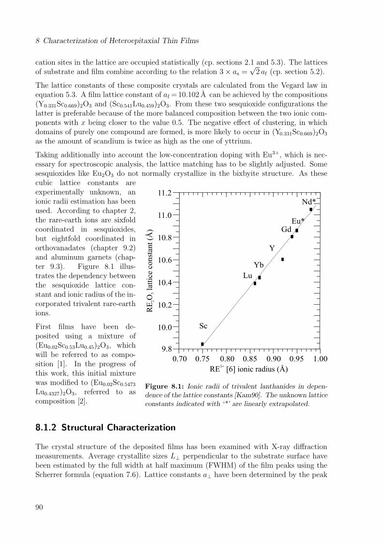
8 Characterization of Heteroepitaxial Thin Films
cation sites in the lattice are occupied statistically (cp. sections 2.1 and 5.3). The latticesof substrate and film combine according to the relation 3× as =
√2 af (cp. section 5.2).
The lattice constants of these composite crystals are calculated from the Vegard law inequation 5.3. A film lattice constant of af =10.102 A can be achieved by the compositions(Y0.331Sc0.669)2O3 and (Sc0.541Lu0.459)2O3. From these two sesquioxide configurations thelatter is preferable because of the more balanced composition between the two ionic com-ponents with x being closer to the value 0.5. The negative effect of clustering, in whichdomains of purely one compound are formed, is more likely to occur in (Y0.331Sc0.669)2O3
as the amount of scandium is twice as high as the one of yttrium.
Taking additionally into account the low-concentration doping with Eu3+, which is nec-essary for spectroscopic analysis, the lattice matching has to be slightly adjusted. Somesesquioxides like Eu2O3 do not normally crystallize in the bixbyite structure. As these
0.70 0.75 0.80 0.859.8
10.0
10.2
10.4
10.6
10.8
11.0
11.2Nd*
Eu*Gd
Y
Lu
Sc
Yb
0.90 0.95 1.00RE [6] ionic radius (Å)3+
RE
O l
atti
ce c
onst
ant
(Å)
23
Figure 8.1: Ionic radii of trivalent lanthanides in depen-dence of the lattice constants [Kam90]. The unknown latticeconstants indicated with ‘*’ are linearly extrapolated.
cubic lattice constants areexperimentally unknown, anionic radii estimation has beenused. According to chapter 2,the rare-earth ions are sixfoldcoordinated in sesquioxides,but eightfold coordinated inorthovanadates (chapter 9.2)and aluminum garnets (chap-ter 9.3). Figure 8.1 illus-trates the dependency betweenthe sesquioxide lattice con-stant and ionic radius of the in-corporated trivalent rare-earthions.
First films have been de-posited using a mixture of(Eu0.02Sc0.53Lu0.45)2O3, whichwill be referred to as compo-sition [1]. In the progress ofthis work, this initial mixturewas modified to (Eu0.02Sc0.5473Lu0.4327)2O3, referred to ascomposition [2].
8.1.2 Structural Characterization
The crystal structure of the deposited films has been examined with X-ray diffractionmeasurements. Average crystallite sizes L⊥ perpendicular to the substrate surface havebeen estimated by the full width at half maximum (FWHM) of the film peaks using theScherrer formula (equation 7.6). Lattice constants a⊥ have been determined by the peak
90
8.1 Composite Sesquioxide Films on Sapphire
positions (cp. chapter 7.1). A list of deposited films with the entire set of deposition pa-rameters is given in appendix A. Due to the continuous improvement of the pulsed laserdeposition setup during this work, the films are tagged in order to distinguish their fabri-cation characteristics. A resistive heater with no direct thermal contact to the substrateand a maximum effective temperature of 750 � C has been used for films < S080. Films≥ S080 have been deposited using a laser-based heater with the substrates mounted on SiCor Si3N4 heat-spreader. In accordance with the insights gained by the work of [Gun07],pre-deposition substrate treatment in combination with atomic force microscopy has beenperformed in the last stage of this work as an additional preparation step for the in-situreflection high-energy electron diffraction measurements during the deposition process.These films are tagged ‘SR’.
In X-ray diffraction polarization effects, divergence, and non-perfect monochromatic radi-ation lead to an intensity attenuation at higher diffraction angles [Kri90, Bur02]. Becauseof this behavior only crystal-planes of lower diffraction order are often detected withsufficient intensity in thin films. To a certain extent the intensity at higher angles alsodepends on the employed X-ray device as in newer apparatuses it is boosted. The lowresolution of higher-order crystal-planes in some measurements has two reasons: First,the device used at the Fachhochschule Wedel is of older age. Second, the film intensitymaximum in the diffraction spectra measured with up-to-date devices at the TechnischeUniversitat Hamburg-Harburg is determined by the highest diffraction peak. All otherdiffraction peaks have an intensity resolution relative to this maximum, which in generalbelongs to the substrate. An exclusion of the substrate peak in the diffraction spectrahas been avoided, as a variation in absolute measuring positions is only obtained withreference to the substrate reflections. This information is essential in order to estimatethe lattice matching correctly. In agreement with this fact, the diffraction measurementanalysis focuses on crystal-planes of lower order, in this case the {222} reflection.Although thickness series with ultra-thin films of some nanometers thickness were alsofabricated in the course of this work (cp. appendix A), emphasis is laid on films with50 nm<dfilm< 100 nm. This is due to the fact that Burmester, Bar, and Rabisch alreadyreported film growth effects in very thin films and assessed that crystalline bulk-likeproperties require film thicknesses of at least 20 nm [Bur02, Bar04, Rab04]. In addition,the analysis of lattice matching is based on pronounced and distinct reflection peaks,which necessitate a certain film thickness.
Figure 8.2 contains X-ray spectra of Eu-doped (Sc, Lu)2O3 films with (a), (b), and (c)belonging to a thickness series fabricated at identical deposition conditions from a sintered(Sc, Lu)2O3 target of composition [1]. Therein, a substrate temperature of T = 700 � C,a constant oxygen pressure of po2 = 7.9 × 10⁻³mbar, and a repetition rate of ν = 10Hzwere used. The collected data are summarized in table 8.1.
91
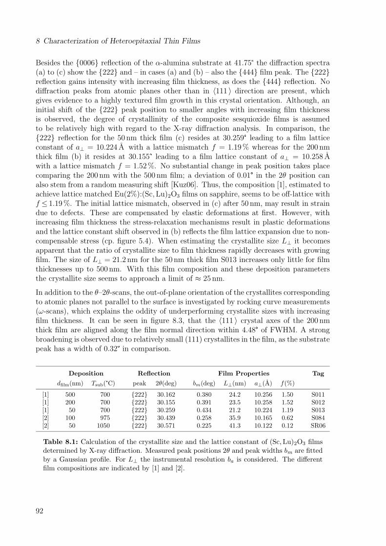
8 Characterization of Heteroepitaxial Thin Films
Besides the {0006} reflection of the α-alumina substrate at 41.75 � the diffraction spectra(a) to (c) show the {222} and – in cases (a) and (b) – also the {444} film peak. The {222}reflection gains intensity with increasing film thickness, as does the {444} reflection. Nodiffraction peaks from atomic planes other than in 〈111 〉 direction are present, whichgives evidence to a highly textured film growth in this crystal orientation. Although, aninitial shift of the {222} peak position to smaller angles with increasing film thicknessis observed, the degree of crystallinity of the composite sesquioxide films is assumedto be relatively high with regard to the X-ray diffraction analysis. In comparison, the{222} reflection for the 50 nm thick film (c) resides at 30.259 � leading to a film latticeconstant of a⊥ = 10.224 A with a lattice mismatch f = 1.19% whereas for the 200 nmthick film (b) it resides at 30.155 � leading to a film lattice constant of a⊥ = 10.258 Awith a lattice mismatch f = 1.52%. No substantial change in peak position takes placecomparing the 200 nm with the 500 nm film; a deviation of 0.01 � in the 2θ position canalso stem from a random measuring shift [Kuz06]. Thus, the composition [1], estimated toachieve lattice matched Eu(2%):(Sc, Lu)2O3 films on sapphire, seems to be off-lattice withf ≤ 1.19%. The initial lattice mismatch, observed in (c) after 50 nm, may result in straindue to defects. These are compensated by elastic deformations at first. However, withincreasing film thickness the stress-relaxation mechanisms result in plastic deformationsand the lattice constant shift observed in (b) reflects the film lattice expansion due to non-compensable stress (cp. figure 5.4). When estimating the crystallite size L⊥ it becomesapparent that the ratio of crystallite size to film thickness rapidly decreases with growingfilm. The size of L⊥ = 21.2 nm for the 50 nm thick film S013 increases only little for filmthicknesses up to 500 nm. With this film composition and these deposition parametersthe crystallite size seems to approach a limit of ≈ 25 nm.
In addition to the θ–2θ-scans, the out-of-plane orientation of the crystallites correspondingto atomic planes not parallel to the surface is investigated by rocking curve measurements(ω-scans), which explains the oddity of underperforming crystallite sizes with increasingfilm thickness. It can be seen in figure 8.3, that the 〈111 〉 crystal axes of the 200 nmthick film are aligned along the film normal direction within 4.48 � of FWHM. A strongbroadening is observed due to relatively small (111) crystallites in the film, as the substratepeak has a width of 0.32 � in comparison.
Deposition Reflection Film Properties Tag
dfilm(nm) Tsub( � C) peak 2θ(deg) bm(deg) L⊥(nm) a⊥(A) f(%)
[1] 500 700 {222} 30.162 0.380 24.2 10.256 1.50 S011[1] 200 700 {222} 30.155 0.391 23.5 10.258 1.52 S012[1] 50 700 {222} 30.259 0.434 21.2 10.224 1.19 S013[2] 100 975 {222} 30.439 0.258 35.9 10.165 0.62 S084[2] 50 1050 {222} 30.571 0.225 41.3 10.122 0.12 SR06
Table 8.1: Calculation of the crystallite size and the lattice constant of (Sc, Lu)2O3 filmsdetermined by X-ray diffraction. Measured peak positions 2θ and peak widths bm are fittedby a Gaussian profile. For L⊥ the instrumental resolution ba is considered. The differentfilm compositions are indicated by [1] and [2].
92
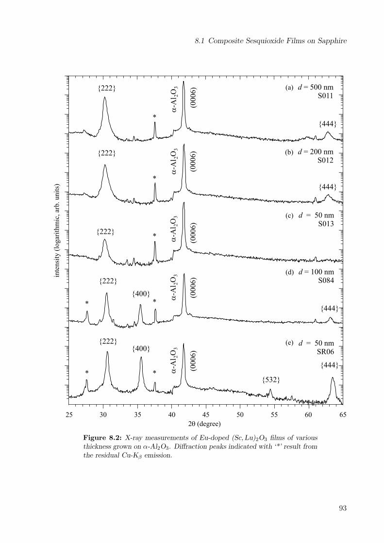
8.1 Composite Sesquioxide Films on Sapphire
25 30 35 40 45 55 60 6550
2 (degree)q
inte
nsi
ty (
logar
ithm
ic, ar
b. unit
s)
d = 50 nmSR06
*
OA
l 23
a- (0
00
6)
OA
l 23
a-
OA
l 23
a-
OA
l 23
a-
(00
06
)(0
00
6)
(00
06
)
{222}
{222}
{444}
*
d = 500 nmS011
d = 200 nmS012
d = 50 nmS013
(a)
(b)
(c)
d = 100 nmS084
(d)
*
OA
l 23
a- (0
00
6)
*
{222}
*{444}
{444}
(e)
{222}
{222}
{400}
{400}
*
*{444}
{532}
Figure 8.2: X-ray measurements of Eu-doped (Sc, Lu)2O3 films of variousthickness grown on α-Al2O3. Diffraction peaks indicated with ‘*’ result fromthe residual Cu-Kβ emission.
93
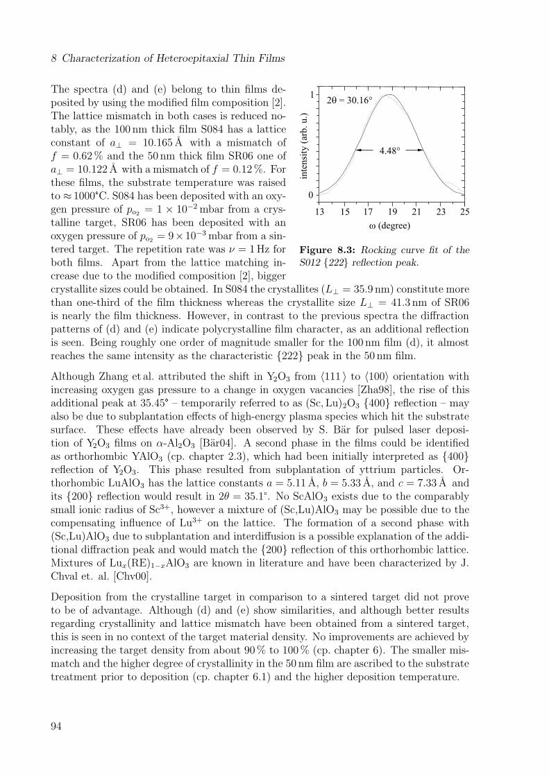
8 Characterization of Heteroepitaxial Thin Films
inte
nsi
ty (
arb
. u
.)
13
0
1
15 17 19 21 23 25
w (degree)
4.48°
2 = 30.16°q
Figure 8.3: Rocking curve fit of theS012 {222} reflection peak.
The spectra (d) and (e) belong to thin films de-posited by using the modified film composition [2].The lattice mismatch in both cases is reduced no-tably, as the 100 nm thick film S084 has a latticeconstant of a⊥ = 10.165 A with a mismatch off = 0.62% and the 50 nm thick film SR06 one ofa⊥ = 10.122 A with a mismatch of f = 0.12%. Forthese films, the substrate temperature was raisedto ≈ 1000 � C. S084 has been deposited with an oxy-gen pressure of po2 = 1 × 10⁻²mbar from a crys-talline target, SR06 has been deposited with anoxygen pressure of po2 = 9×10⁻³mbar from a sin-tered target. The repetition rate was ν = 1Hz forboth films. Apart from the lattice matching in-crease due to the modified composition [2], biggercrystallite sizes could be obtained. In S084 the crystallites (L⊥ = 35.9 nm) constitute morethan one-third of the film thickness whereas the crystallite size L⊥ = 41.3 nm of SR06is nearly the film thickness. However, in contrast to the previous spectra the diffractionpatterns of (d) and (e) indicate polycrystalline film character, as an additional reflectionis seen. Being roughly one order of magnitude smaller for the 100 nm film (d), it almostreaches the same intensity as the characteristic {222} peak in the 50 nm film.
Although Zhang et al. attributed the shift in Y2O3 from 〈111 〉 to 〈100〉 orientation withincreasing oxygen gas pressure to a change in oxygen vacancies [Zha98], the rise of thisadditional peak at 35.45 � – temporarily referred to as (Sc, Lu)2O3 {400} reflection – mayalso be due to subplantation effects of high-energy plasma species which hit the substratesurface. These effects have already been observed by S. Bar for pulsed laser deposi-tion of Y2O3 films on α-Al2O3 [Bar04]. A second phase in the films could be identifiedas orthorhombic YAlO3 (cp. chapter 2.3), which had been initially interpreted as {400}reflection of Y2O3. This phase resulted from subplantation of yttrium particles. Or-thorhombic LuAlO3 has the lattice constants a = 5.11 A, b = 5.33 A, and c = 7.33 A andits {200} reflection would result in 2θ = 35.1 � . No ScAlO3 exists due to the comparablysmall ionic radius of Sc3+, however a mixture of (Sc,Lu)AlO3 may be possible due to thecompensating influence of Lu3+ on the lattice. The formation of a second phase with(Sc,Lu)AlO3 due to subplantation and interdiffusion is a possible explanation of the addi-tional diffraction peak and would match the {200} reflection of this orthorhombic lattice.Mixtures of Lux(RE)1−xAlO3 are known in literature and have been characterized by J.Chval et. al. [Chv00].
Deposition from the crystalline target in comparison to a sintered target did not proveto be of advantage. Although (d) and (e) show similarities, and although better resultsregarding crystallinity and lattice mismatch have been obtained from a sintered target,this is seen in no context of the target material density. No improvements are achieved byincreasing the target density from about 90% to 100% (cp. chapter 6). The smaller mis-match and the higher degree of crystallinity in the 50 nm film are ascribed to the substratetreatment prior to deposition (cp. chapter 6.1) and the higher deposition temperature.
94
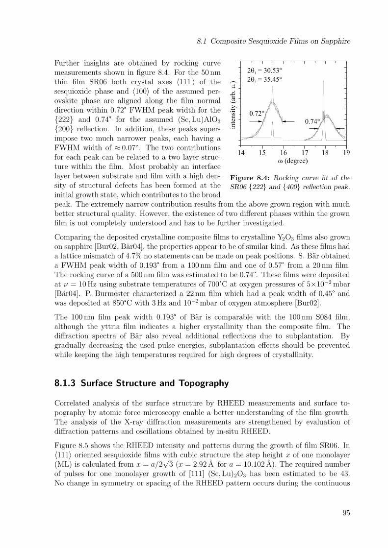
8.1 Composite Sesquioxide Films on Sapphire
inte
nsi
ty (
arb
. u
.)
14 15 16 17 18 19
w (degree)
0.72°
2 = 30.53°q1
2 = 35.45°q2
0.74°
Figure 8.4: Rocking curve fit of theSR06 {222} and {400} reflection peak.
Further insights are obtained by rocking curvemeasurements shown in figure 8.4. For the 50 nmthin film SR06 both crystal axes 〈111 〉 of thesesquioxide phase and 〈100〉 of the assumed per-ovskite phase are aligned along the film normaldirection within 0.72 � FWHM peak width for the{222} and 0.74 � for the assumed (Sc, Lu)AlO3
{200} reflection. In addition, these peaks super-impose two much narrower peaks, each having aFWHM width of ≈ 0.07 � . The two contributionsfor each peak can be related to a two layer struc-ture within the film. Most probably an interfacelayer between substrate and film with a high den-sity of structural defects has been formed at theinitial growth state, which contributes to the broadpeak. The extremely narrow contribution results from the above grown region with muchbetter structural quality. However, the existence of two different phases within the grownfilm is not completely understood and has to be further investigated.
Comparing the deposited crystalline composite films to crystalline Y2O3 films also grownon sapphire [Bur02, Bar04], the properties appear to be of similar kind. As these films hada lattice mismatch of 4.7% no statements can be made on peak positions. S. Bar obtaineda FWHM peak width of 0.193 � from a 100 nm film and one of 0.57 � from a 20 nm film.The rocking curve of a 500 nm film was estimated to be 0.74 � . These films were depositedat ν = 10Hz using substrate temperatures of 700 � C at oxygen pressures of 5×10⁻²mbar[Bar04]. P. Burmester characterized a 22 nm film which had a peak width of 0.45 � andwas deposited at 850 � C with 3Hz and 10−2mbar of oxygen atmosphere [Bur02].
The 100 nm film peak width 0.193 � of Bar is comparable with the 100 nm S084 film,although the yttria film indicates a higher crystallinity than the composite film. Thediffraction spectra of Bar also reveal additional reflections due to subplantation. Bygradually decreasing the used pulse energies, subplantation effects should be preventedwhile keeping the high temperatures required for high degrees of crystallinity.
8.1.3 Surface Structure and Topography
Correlated analysis of the surface structure by RHEED measurements and surface to-pography by atomic force microscopy enable a better understanding of the film growth.The analysis of the X-ray diffraction measurements are strengthened by evaluation ofdiffraction patterns and oscillations obtained by in-situ RHEED.
Figure 8.5 shows the RHEED intensity and patterns during the growth of film SR06. In〈111〉 oriented sesquioxide films with cubic structure the step height x of one monolayer(ML) is calculated from x = a/2
√3 (x = 2.92 A for a = 10.102 A). The required number
of pulses for one monolayer growth of [111] (Sc, Lu)2O3 has been estimated to be 43.No change in symmetry or spacing of the RHEED pattern occurs during the continuous
95
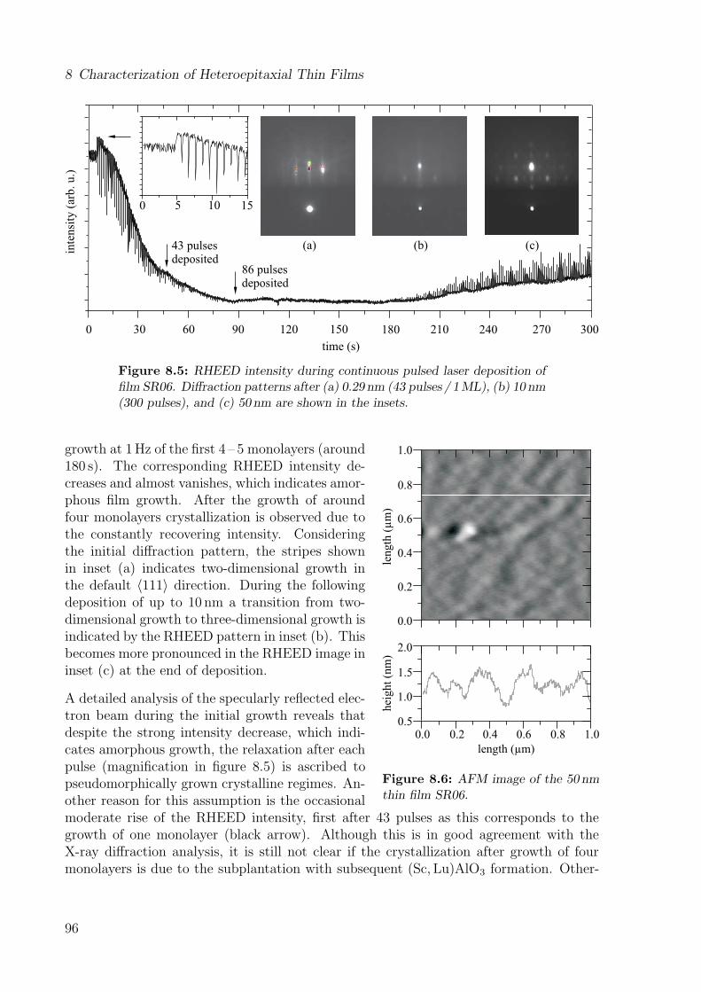
8 Characterization of Heteroepitaxial Thin Filmsin
tensi
ty (
arb. u.)
0 30 60 90 120 180 210150
time (s)
240 270 300
0 5 10 15
43 pulsesdeposited
86 pulsesdeposited
(a) (b) (c)
Figure 8.5: RHEED intensity during continuous pulsed laser deposition offilm SR06. Diffraction patterns after (a) 0.29 nm (43 pulses / 1ML), (b) 10 nm(300 pulses), and (c) 50 nm are shown in the insets.
0.0 0.2 0.4 0.6 0.8 1.00.5
1.0
1.5
2.0
0.0
0.2
0.4
0.6
0.8
1.0
length (µm)
hei
gh
t (n
m)
len
gth
(µ
m)
Figure 8.6: AFM image of the 50 nmthin film SR06.
growth at 1Hz of the first 4 – 5 monolayers (around180 s). The corresponding RHEED intensity de-creases and almost vanishes, which indicates amor-phous film growth. After the growth of aroundfour monolayers crystallization is observed due tothe constantly recovering intensity. Consideringthe initial diffraction pattern, the stripes shownin inset (a) indicates two-dimensional growth inthe default 〈111〉 direction. During the followingdeposition of up to 10 nm a transition from two-dimensional growth to three-dimensional growth isindicated by the RHEED pattern in inset (b). Thisbecomes more pronounced in the RHEED image ininset (c) at the end of deposition.
A detailed analysis of the specularly reflected elec-tron beam during the initial growth reveals thatdespite the strong intensity decrease, which indi-cates amorphous growth, the relaxation after eachpulse (magnification in figure 8.5) is ascribed topseudomorphically grown crystalline regimes. An-other reason for this assumption is the occasionalmoderate rise of the RHEED intensity, first after 43 pulses as this corresponds to thegrowth of one monolayer (black arrow). Although this is in good agreement with theX-ray diffraction analysis, it is still not clear if the crystallization after growth of fourmonolayers is due to the subplantation with subsequent (Sc, Lu)AlO3 formation. Other-
96
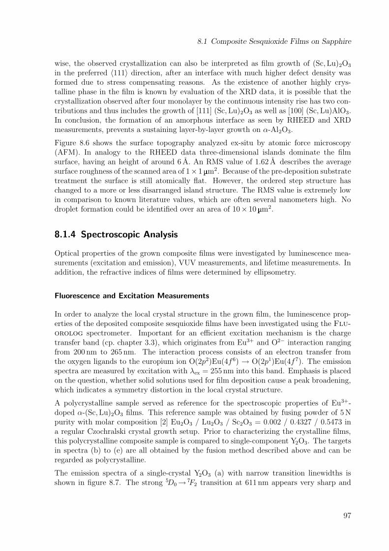
8.1 Composite Sesquioxide Films on Sapphire
wise, the observed crystallization can also be interpreted as film growth of (Sc, Lu)2O3
in the preferred 〈111〉 direction, after an interface with much higher defect density wasformed due to stress compensating reasons. As the existence of another highly crys-talline phase in the film is known by evaluation of the XRD data, it is possible that thecrystallization observed after four monolayer by the continuous intensity rise has two con-tributions and thus includes the growth of [111] (Sc, Lu)2O3 as well as [100] (Sc, Lu)AlO3.In conclusion, the formation of an amorphous interface as seen by RHEED and XRDmeasurements, prevents a sustaining layer-by-layer growth on α-Al2O3.
Figure 8.6 shows the surface topography analyzed ex-situ by atomic force microscopy(AFM). In analogy to the RHEED data three-dimensional islands dominate the filmsurface, having an height of around 6 A. An RMS value of 1.62 A describes the averagesurface roughness of the scanned area of 1× 1 � m2. Because of the pre-deposition substratetreatment the surface is still atomically flat. However, the ordered step structure haschanged to a more or less disarranged island structure. The RMS value is extremely lowin comparison to known literature values, which are often several nanometers high. Nodroplet formation could be identified over an area of 10× 10 � m2.
8.1.4 Spectroscopic Analysis
Optical properties of the grown composite films were investigated by luminescence mea-surements (excitation and emission), VUV measurements, and lifetime measurements. Inaddition, the refractive indices of films were determined by ellipsometry.
Fluorescence and Excitation Measurements
In order to analyze the local crystal structure in the grown film, the luminescence prop-erties of the deposited composite sesquioxide films have been investigated using the Flu-orolog spectrometer. Important for an efficient excitation mechanism is the chargetransfer band (cp. chapter 3.3), which originates from Eu3+ and O2− interaction rangingfrom 200 nm to 265 nm. The interaction process consists of an electron transfer fromthe oxygen ligands to the europium ion O(2p2)Eu(4f 6) → O(2p1)Eu(4f 7). The emissionspectra are measured by excitation with λex = 255 nm into this band. Emphasis is placedon the question, whether solid solutions used for film deposition cause a peak broadening,which indicates a symmetry distortion in the local crystal structure.
A polycrystalline sample served as reference for the spectroscopic properties of Eu3+-doped α-(Sc, Lu)2O3 films. This reference sample was obtained by fusing powder of 5Npurity with molar composition [2] Eu2O3 / Lu2O3 / Sc2O3 = 0.002 / 0.4327 / 0.5473 ina regular Czochralski crystal growth setup. Prior to characterizing the crystalline films,this polycrystalline composite sample is compared to single-component Y2O3. The targetsin spectra (b) to (e) are all obtained by the fusion method described above and can beregarded as polycrystalline.
The emission spectra of a single-crystal Y2O3 (a) with narrow transition linewidths isshown in figure 8.7. The strong 5D0→ 7F2 transition at 611 nm appears very sharp and
97
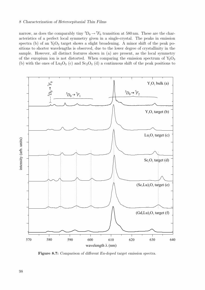
8 Characterization of Heteroepitaxial Thin Films
narrow, as does the comparably tiny 5D0→ 7F0 transition at 580 nm. These are the char-acteristics of a perfect local symmetry given in a single-crystal. The peaks in emissionspectra (b) of an Y2O3 target shows a slight broadening. A minor shift of the peak po-sitions to shorter wavelengths is observed, due to the lower degree of crystallinity in thesample. However, all distinct features shown in (a) are present, as the local symmetryof the europium ion is not distorted. When comparing the emission spectrum of Y2O3
(b) with the ones of Lu2O3 (c) and Sc2O3 (d) a continuous shift of the peak positions to
inte
nsi
ty (
arb. unit
s)
570 580 590 600 610 620 640630
wavelength (nm)l
®5D0
7F2
®5 D
07 F
0
®5D0
7F1
Y O bulk2 3 (a)
Y O target2 3 (b)
Lu O2 3 target (c)
Sc O2 3 target (d)
(Sc,Lu) O2 3 target (e)
(Gd,Lu) O2 3 target (f)
Figure 8.7: Comparison of different Eu-doped target emission spectra.
98
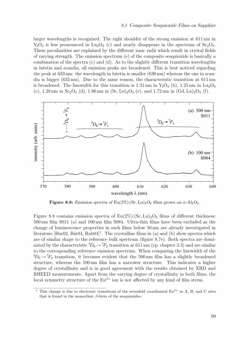
8.1 Composite Sesquioxide Films on Sapphire
larger wavelengths is recognized. The right shoulder of the strong emission at 611 nm inY2O3 is less pronounced in Lu2O3 (c) and nearly disappears in the spectrum of Sc2O3.These peculiarities are explained by the different ionic radii which result in crystal fieldsof varying strength. The emission spectrum (e) of the composite sesquioxide is basically acombination of the spectra (c) and (d). As to the slightly different transition wavelengthsin lutetia and scandia, all emission peaks are broadened. This is best noticed regardingthe peak at 633 nm: the wavelength in lutetia is smaller (630 nm) whereas the one in scan-dia is bigger (635 nm). Due to the same reason, the characteristic transition at 611 nmis broadened. The linewidth for this transition is 1.31 nm in Y2O3 (b), 1.25 nm in Lu2O3
(c), 1.28 nm in Sc2O3 (d), 1.86 nm in (Sc, Lu)2O3 (e), and 1.72 nm in (Gd, Lu)2O3 (f).
(a) 500 nmS011
(b) 100 nmS084in
tensi
ty (
arb. unit
s)
570 580 590 600 610 620 640630
wavelength (nm)l
®5D0
7F2
®5 D
07 F
0
®5D0
7F1
Figure 8.8: Emission spectra of Eu(2%):(Sc, Lu)2O3 films grown on α-Al2O3.
Figure 8.8 contains emission spectra of Eu(2%):(Sc, Lu)2O3 films of different thickness:500 nm film S011 (a) and 100 nm film S084. Ultra-thin films have been excluded as thechange of luminescence properties in such films below 50 nm are already investigated inliterature [Bur02, Bar04, Rab04]1. The crystalline films in (a) and (b) show spectra whichare of similar shape to the reference bulk spectrum (figure 8.7e). Both spectra are domi-nated by the characteristic 5D0→ 7F2 transition at 611 nm (cp. chapter 3.3) and are similarto the corresponding reference emission spectrum. When comparing the linewidth of the5D0→ 7F2 transition, it becomes evident that the 500 nm film has a slightly broadenedstructure, whereas the 100 nm film has a narrower structure. This indicates a higherdegree of crystallinity and is in good agreement with the results obtained by XRD andRHEED measurements. Apart from the varying degree of crystallinity in both films, thelocal symmetry structure of the Eu3+ ion is not affected by any kind of film stress.
1 This change is due to electronic transitions of the sevenfold coordinated Eu3+ in A, B, and C sitesthat is found in the monoclinic β-form of the sesquioxides.
99
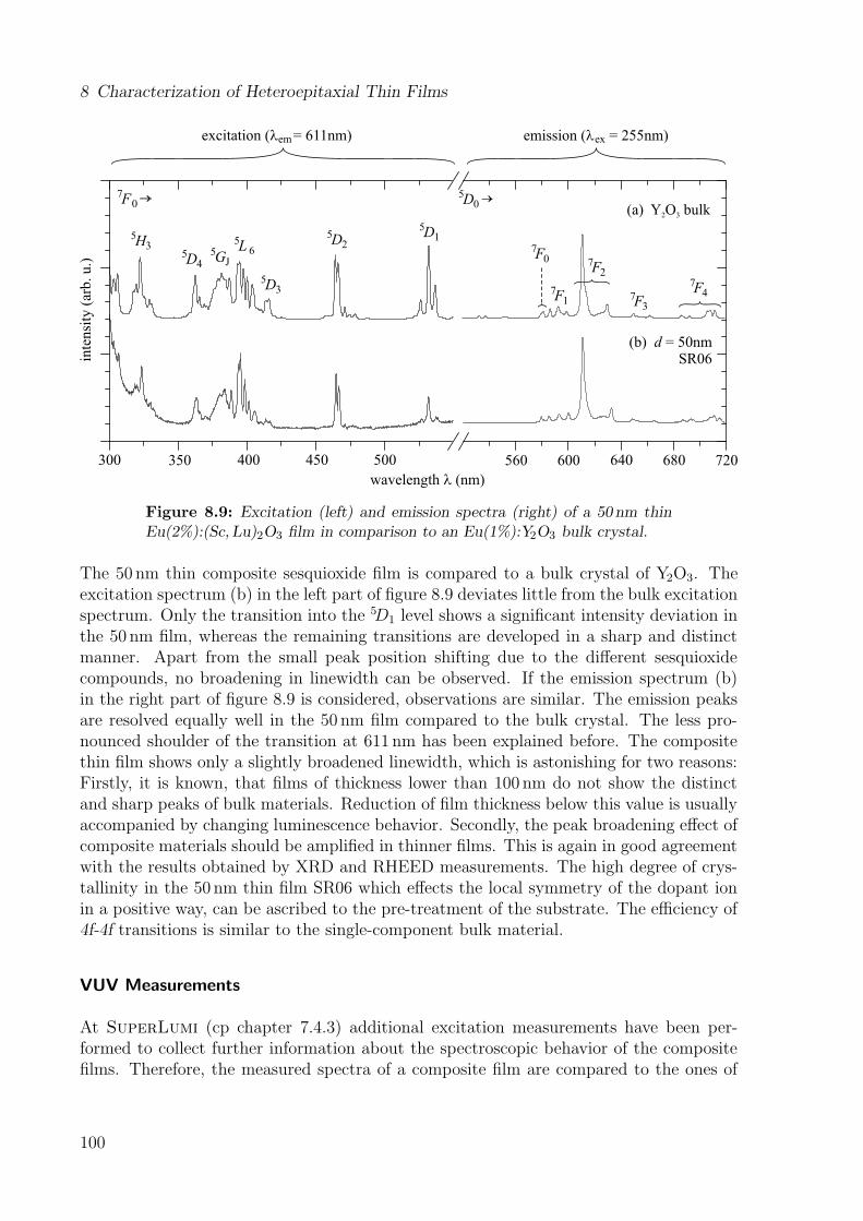
8 Characterization of Heteroepitaxial Thin Films
wavelength (nm)l
300 350 400 450 600 640 680 720
(a) Y O bulk2 3
(b) = 50nmSR06
d
inte
nsi
ty (
arb
. u
.)
excitation ( = 611nm)lem emission ( = 255nm)lex
560
5D1
7F0
5D2
5D3
5L 65
GJ5D4
5H3
500
7F2
®5D0
7F3
7F4
®7F0
7F1
Figure 8.9: Excitation (left) and emission spectra (right) of a 50 nm thinEu(2%):(Sc, Lu)2O3 film in comparison to an Eu(1%):Y2O3 bulk crystal.
The 50 nm thin composite sesquioxide film is compared to a bulk crystal of Y2O3. Theexcitation spectrum (b) in the left part of figure 8.9 deviates little from the bulk excitationspectrum. Only the transition into the 5D1 level shows a significant intensity deviation inthe 50 nm film, whereas the remaining transitions are developed in a sharp and distinctmanner. Apart from the small peak position shifting due to the different sesquioxidecompounds, no broadening in linewidth can be observed. If the emission spectrum (b)in the right part of figure 8.9 is considered, observations are similar. The emission peaksare resolved equally well in the 50 nm film compared to the bulk crystal. The less pro-nounced shoulder of the transition at 611 nm has been explained before. The compositethin film shows only a slightly broadened linewidth, which is astonishing for two reasons:Firstly, it is known, that films of thickness lower than 100 nm do not show the distinctand sharp peaks of bulk materials. Reduction of film thickness below this value is usuallyaccompanied by changing luminescence behavior. Secondly, the peak broadening effect ofcomposite materials should be amplified in thinner films. This is again in good agreementwith the results obtained by XRD and RHEED measurements. The high degree of crys-tallinity in the 50 nm thin film SR06 which effects the local symmetry of the dopant ionin a positive way, can be ascribed to the pre-treatment of the substrate. The efficiency of4f-4f transitions is similar to the single-component bulk material.
VUV Measurements
At SuperLumi (cp chapter 7.4.3) additional excitation measurements have been per-formed to collect further information about the spectroscopic behavior of the compositefilms. Therefore, the measured spectra of a composite film are compared to the ones of
100
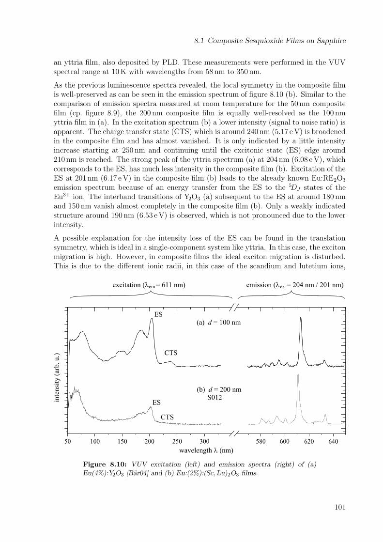
8.1 Composite Sesquioxide Films on Sapphire
an yttria film, also deposited by PLD. These measurements were performed in the VUVspectral range at 10K with wavelengths from 58 nm to 350 nm.
As the previous luminescence spectra revealed, the local symmetry in the composite filmis well-preserved as can be seen in the emission spectrum of figure 8.10 (b). Similar to thecomparison of emission spectra measured at room temperature for the 50 nm compositefilm (cp. figure 8.9), the 200 nm composite film is equally well-resolved as the 100 nmyttria film in (a). In the excitation spectrum (b) a lower intensity (signal to noise ratio) isapparent. The charge transfer state (CTS) which is around 240 nm (5.17 eV) is broadenedin the composite film and has almost vanished. It is only indicated by a little intensityincrease starting at 250 nm and continuing until the excitonic state (ES) edge around210 nm is reached. The strong peak of the yttria spectrum (a) at 204 nm (6.08 eV), whichcorresponds to the ES, has much less intensity in the composite film (b). Excitation of theES at 201 nm (6.17 eV) in the composite film (b) leads to the already known Eu:RE2O3
emission spectrum because of an energy transfer from the ES to the 5DJ states of theEu3+ ion. The interband transitions of Y2O3 (a) subsequent to the ES at around 180 nmand 150 nm vanish almost completely in the composite film (b). Only a weakly indicatedstructure around 190 nm (6.53 eV) is observed, which is not pronounced due to the lowerintensity.
A possible explanation for the intensity loss of the ES can be found in the translationsymmetry, which is ideal in a single-component system like yttria. In this case, the excitonmigration is high. However, in composite films the ideal exciton migration is disturbed.This is due to the different ionic radii, in this case of the scandium and lutetium ions,
(b) = 200 nmS012d
50 100 150 200 250 300 580 600 620 640
wavelength (nm)l
inte
nsi
ty (
arb
. u
.)
(a) = 100 nmd
ES
CTS
excitation ( = 611 nm)lem emission ( = 204 nm / 201 nm)lex
ES
CTS
Figure 8.10: VUV excitation (left) and emission spectra (right) of (a)Eu(4%):Y2O3 [Bar04] and (b) Eu:(2%):(Sc, Lu)2O3 films.
101
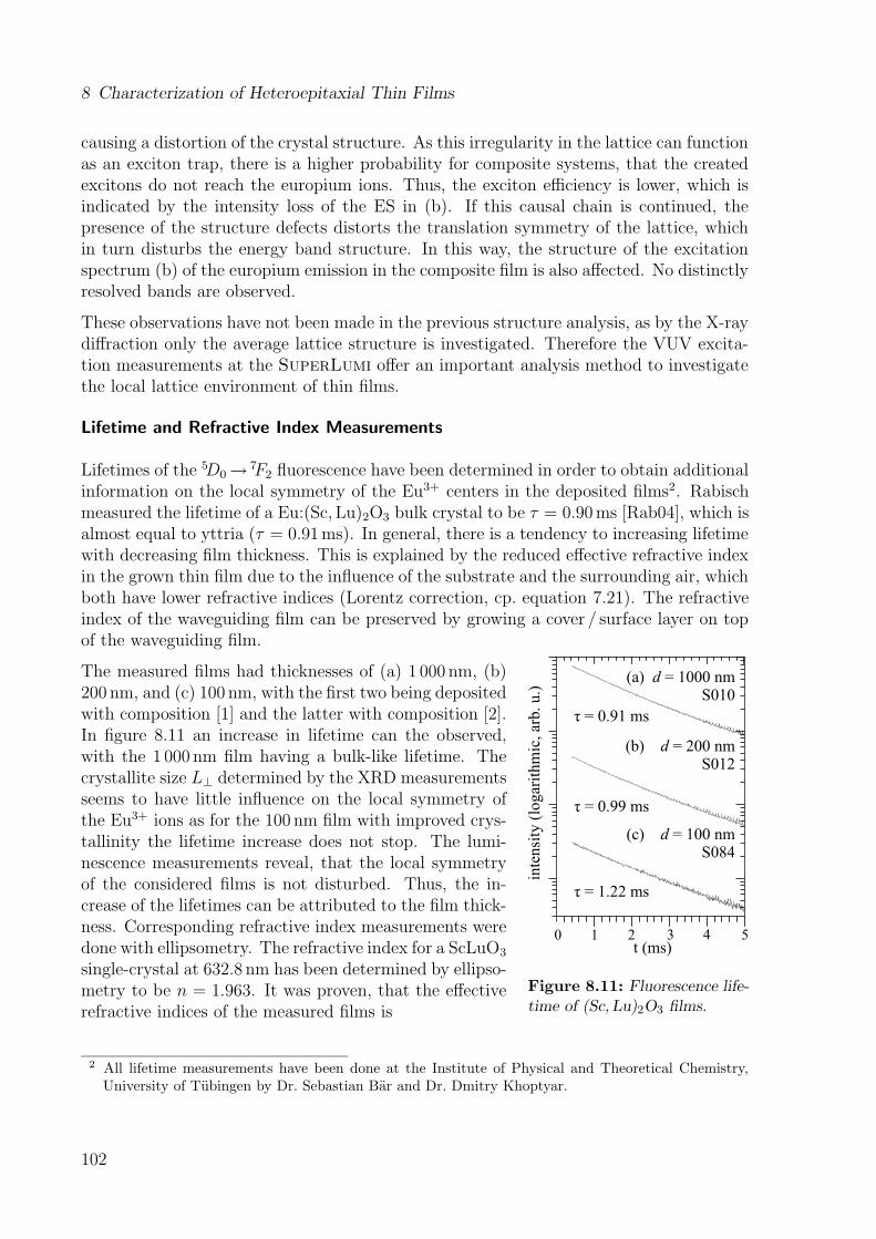
8 Characterization of Heteroepitaxial Thin Films
causing a distortion of the crystal structure. As this irregularity in the lattice can functionas an exciton trap, there is a higher probability for composite systems, that the createdexcitons do not reach the europium ions. Thus, the exciton efficiency is lower, which isindicated by the intensity loss of the ES in (b). If this causal chain is continued, thepresence of the structure defects distorts the translation symmetry of the lattice, whichin turn disturbs the energy band structure. In this way, the structure of the excitationspectrum (b) of the europium emission in the composite film is also affected. No distinctlyresolved bands are observed.
These observations have not been made in the previous structure analysis, as by the X-raydiffraction only the average lattice structure is investigated. Therefore the VUV excita-tion measurements at the SuperLumi offer an important analysis method to investigatethe local lattice environment of thin films.
Lifetime and Refractive Index Measurements
Lifetimes of the 5D0→ 7F2 fluorescence have been determined in order to obtain additionalinformation on the local symmetry of the Eu3+ centers in the deposited films2. Rabischmeasured the lifetime of a Eu:(Sc, Lu)2O3 bulk crystal to be τ = 0.90ms [Rab04], which isalmost equal to yttria (τ = 0.91ms). In general, there is a tendency to increasing lifetimewith decreasing film thickness. This is explained by the reduced effective refractive indexin the grown thin film due to the influence of the substrate and the surrounding air, whichboth have lower refractive indices (Lorentz correction, cp. equation 7.21). The refractiveindex of the waveguiding film can be preserved by growing a cover / surface layer on top
0 1 4 52 3t (ms)
inte
nsi
ty (
log
arit
hm
ic,
arb
. u
.)
ô = 0.91 ms
ô = 1.22 ms
(a) = 1000 nmS010
d
(c) = 100 nmS084
d
(b) = 200 nmS012
d
ô = 0.99 ms
Figure 8.11: Fluorescence life-time of (Sc, Lu)2O3 films.
of the waveguiding film.
The measured films had thicknesses of (a) 1 000 nm, (b)200 nm, and (c) 100 nm, with the first two being depositedwith composition [1] and the latter with composition [2].In figure 8.11 an increase in lifetime can the observed,with the 1 000 nm film having a bulk-like lifetime. Thecrystallite size L⊥ determined by the XRD measurementsseems to have little influence on the local symmetry ofthe Eu3+ ions as for the 100 nm film with improved crys-tallinity the lifetime increase does not stop. The lumi-nescence measurements reveal, that the local symmetryof the considered films is not disturbed. Thus, the in-crease of the lifetimes can be attributed to the film thick-ness. Corresponding refractive index measurements weredone with ellipsometry. The refractive index for a ScLuO3
single-crystal at 632.8 nm has been determined by ellipso-metry to be n = 1.963. It was proven, that the effectiverefractive indices of the measured films is
2 All lifetime measurements have been done at the Institute of Physical and Theoretical Chemistry,University of Tubingen by Dr. Sebastian Bar and Dr. Dmitry Khoptyar.
102
8.2 Sapphire Films on Composite Sesquioxide
reduced, as predicted by the theory. The 1 000 nm Eu:(Sc.Lu)2O3 film had a refractiveindex of n = 1.957, which is almost the bulk value, whereas the 200 nm and 100 nm filmsshow reduced refractive indices of n = 1.955 and n = 1.942, respectively. The resulting∆n = 0.2 for this substrate–film system is suited for waveguide applications.
8.2 Sapphire Films on Composite Sesquioxide
In this section the growth of sapphire films on a composite sesquioxide substrate is investi-gated. It is the reverse experiment of section 8.1. Although the analysis of the compositesesquioxide films in the previous section showed highly textured crystalline growth in thepreferred {111} direction, it was not possible to achieve continuous layer-by-layer growth.Consequently this section investigates whether layer-by-layer film growth can be obtainedusing a composite sesquioxide material as substrate with a single-component film.
Due to the ionic radii difference between aluminum and europium (cp. table 3.1), with theeuropium ion having almost twice the radius of aluminum in sixfold coordination, it is notpossible to use a Eu-doping in this case. Thus, in order to investigate the luminescenceproperties of the grown films, chromium is used as dopant ion. Consequently, the filmlayer consists of Al2O3 doped with Cr3+ whereas the substrate material is ScLuO3 withequal amount of each sesquioxide component. The mixed sesquioxide substrates wereprepared from a bulk crystal grown at the Institute of Laser Physics by the HEM growthtechnique (cp. page 8) and have a (111) orientation of the surface.
8.2.1 Lattice Matching and Structural Characterization
In this case the sesquioxide solid solution offers a threefold symmetry axis (hexagonalstructure) in the cubic {111}-planes. The Al2O3 film can grow in vertical direction forminga (0001) surface. Similar to section 8.1 the lattices of substrate and film combine accordingto the relation 3×af =
√2 as (cp. section 5.2). By using equation 5.3 the lattice constant of
the (Sc0.5Lu0.5)2O3 substrate is determined to be aScLuO3= 10.124 A. With a Cr3+-doping
of 0.5% the lattice constant3 of the (Cr0.05Al0.95)2O3 film is estimated to be aCr:Al2O3=
4.772 A and cCr:Al2O3= 13.024 A. This leads to a theoretical lattice mismatch of f =
−0.01% relative to the substrate, which is considerably small.
Figure 8.12 shows the diffraction measurements for two 100 nm thin Cr(0.5%):Al2O3 filmsdeposited under different conditions. Primarily, the temperature of the substrate wasvaried from 700 � C (a) to 950 � C (b), whereas the oxygen pressure was almost identicalwith 8.5×10⁻³mbar in the first deposition and 1×10⁻²mbar in the second one. Thedeposition was carried out with 3Hz (a) and 1Hz (b). Table 8.2 summarizes the dataobtained by the diffraction measurements.
Besides the {222} reflection of the sesquioxide substrate at 30.55 � , a distinct {0006}reflection at 41.805 � can be seen in (a). The intensity of this film reflection is not as high
3 The lattice constants of hexagonal α-Cr2O3 are a = 4.953 A and c = 13.578 A [Bel03].
103
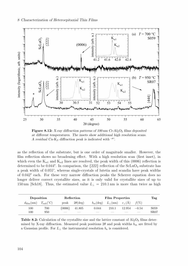
8 Characterization of Heteroepitaxial Thin Films
25 30 35 40 45 55 60 6550
2 (degree)q
inte
nsi
ty (
logar
ithm
ic, ar
b. unit
s)
(0006)
*
T = 700 °CS059
T = 950 °CSR07
(a)
(b)
{2
22
}
ScL
uO
3
{2
22
}
ScL
uO
3
{4
44
}
inte
nsi
ty (
arb. u.)
41.2 41.6 42.0 42.4
Ka2
Ka1
inte
nsi
ty (
arb. u.)
30 3130.5
Ka2
Ka1
inte
nsi
ty (
arb. u.)
52 53 54 55
Ka2
Ka1
Figure 8.12: X-ray diffraction patterns of 100 nm Cr:Al2O3 films depositedat different temperatures. The insets show additional high resolution scans.A residual Cu-Kβ diffraction peak is indicated with ‘*’.
as the reflection of the substrate, but is one order of magnitude smaller. However, thefilm reflection shows no broadening effect. With a high resolution scan (first inset), inwhich even the Kα1 and Kα2 lines are resolved, the peak width of this (0006) reflection isdetermined to be 0.044 � . In comparison, the {222} reflection of the ScLuO3 substrate hasa peak width of 0.055 � , whereas single-crystals of lutetia and scandia have peak widthsof 0.042 � each. For these very narrow diffraction peaks the Scherrer equation does nolonger deliver correct crystallite sizes, as it is only valid for crystallite sizes of up to150 nm [Sch18]. Thus, the estimated value L⊥ = 210.1 nm is more than twice as high
Deposition Reflection Film Properties Tag
dfilm(nm) Tsub( � C) peak 2θ(deg) bm(deg) L⊥(nm) c⊥(A) f(%)
100 700 {0006} 41.805 0.044 210.1 12.954 −0.54 S059100 950 — — — — — — SR07
Table 8.2: Calculation of the crystallite size and the lattice constant of Al2O3 films deter-mined by X-ray diffraction. Measured peak positions 2θ and peak widths bm are fitted bya Gaussian profile. For L⊥ the instrumental resolution ba is considered.
104
8.2 Sapphire Films on Composite Sesquioxide
as the grown film thickness. Due to the very distinct shape of the (0006) reflection, itslinewidth, and no indication of broadening, it can be assumed that the deposited Cr:Al2O3
film is entirely crystalline. Estimating the lattice constant in c-axis of the film deliversc = 12.954 A which is −0.54% smaller than the substrate value.
Unfortunately, no (0006) reflection is seen in the spectrum (b). This is contrary to whatwas expected, as the deposition parameters thought to be optimal with regard to therepetition rate and the temperature. A temperature of 950 � C should be preferable dueto the higher mobility of the deposited atoms. The lower repetition rate increases thediffusion length. Both changes should effect the film growth in a positive way. How-ever, despite pre-deposition annealing of the substrate no atomically ordered surface withterraces of atomic height could be obtained, which may indicate poor substrate quality(high miscut). The left inset in figure 8.12 (b) reveals an additional peak to the usual Kα1,Kα2-line splitting in the {222} reflection at around 2θ = 30.5 � . Even better observablein the {444} reflection (right inset), an additional film reflection is seen at 2θ = 63.37 � .Considering the results of the reverse substrate–film system in the previous section 8.1,the probability of subplantation leading to the same (Sc, Lu)AlO3 perovskite phase isgiven. This reflection has a FWHM peak width of 0.33 � and could correspond to the{222} reflection of (Sc, Lu)AlO3 with a lattice constant of a(Sc,Lu)AlO3
= 5.085 A. LuAlO3
has an orthorhombic crystal structure with a lattice constant of aLuAlO3= 5.11 A and
a 6= b 6= c. As the incorporation of scandium particles would result in a smaller lat-tice constant this interpretation seems quite possible. Due to the very high substratetemperatures subplantation and interdiffusion of Al2O3 into the ScLuO3 matrix is likelyto occur. In addition, solid solutions like ScLuO3 have reduced material hardness andmelting points. This is caused by modification of the bonding forces. Apart from sub-plantation effects, solid-state reactions may occur at half the melting temperature. Dueto these reasons, temperatures of around 700 � C seem appropriate for mixed sesquioxidesubstrates. Further research should be invested in this system with better composite sub-strates using lower deposition temperatures.
8.2.2 Surface Structure and Topography
The RHEED measurements in figure 8.13(a) reveal similar yet different growth behaviorcompared with composite sesquioxide films on sapphire (cp section 8.1.3). Typical char-acteristics are the intensity fall during initial growth (amorphous interface), relaxationafter each pulse (pseudomorphically grown crystalline regimes), and occasional moderateintensity rise (monolayer completion). For the Al2O3 film material the growth of onemonolayer (2.2 A) requires 48 pulses (black arrow). However, no crystallization is ob-served as the intensity does not recover. The pulse relaxation seen at initial depositionalso vanishes together with the overall intensity and is less pronounced in contrast tothe Eu:(Sc, Lu)2O3 RHEED oscillations for the initial deposition (cp. figure 8.5). Theresulting diffraction pattern after deposition (right inset, figure 8.13) is vague and notclearly associable to the known RHEED patterns. The distinct diffraction points seen inthe initial RHEED image (left inset, figure 8.13a) have almost vanished.
The post-deposition surface topography has been determined to be very smooth and
105
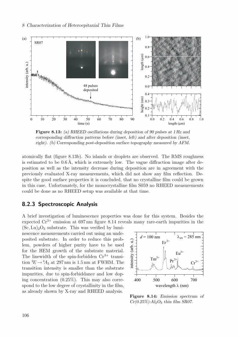
8 Characterization of Heteroepitaxial Thin Filmsin
tensi
ty (
arb. u.)
0 10 20 30 40 60 7050time (s)
80 90 0.0 0.2 0.4 0.6 0.8 1.00.1
0.2
0.3
0.4
0.0
0.2
0.4
0.6
0.8
1.0
length (µm)
hei
ght
(nm
)le
ngth
(µ
m)
(a) (b)
48 pulsesdeposited
SR07
Figure 8.13: (a) RHEED oscillations during deposition of 90 pulses at 1Hz andcorresponding diffraction patterns before (inset, left) and after deposition (inset,right). (b) Corresponding post-deposition surface topography measured by AFM.
atomically flat (figure 8.13b). No islands or droplets are observed. The RMS roughnessis estimated to be 0.6 A, which is extremely low. The vague diffraction image after de-position as well as the intensity decrease during deposition are in agreement with thepreviously evaluated X-ray measurements, which did not show any film reflection. De-spite the good surface properties it is concluded, that no crystalline film could be grownin this case. Unfortunately, for the monocrystalline film S059 no RHEED measurementscould be done as no RHEED setup was available at that time.
8.2.3 Spectroscopic Analysis
A brief investigation of luminescence properties was done for this system. Besides theexpected Cr3+ emission at 697 nm figure 8.14 reveals many rare-earth impurities in the
d = 100 nm
wavelength (nm)l
600 700400
inte
nsi
ty (
arb. u.)
l = 285 nmex
500
3+Tm
3+Er
3+Pr
3+Eu
3+Cr
Figure 8.14: Emission spectrum ofCr(0.25%):Al2O3 thin film SR07.
(Sc, Lu)2O3 substrate. This was verified by lumi-nescence measurements carried out using an unde-posited substrate. In order to reduce this prob-lem, powders of higher purity have to be usedfor the HEM growth of the substrate material.The linewidth of the spin-forbidden Cr3+ transi-tion 2E→ 4A2 at 297 nm is 1.5 nm at FWHM. Thetransition intensity is smaller than the substrateimpurities, due to spin-forbiddance and low dop-ing concentration (0.25%). This may also corre-spond to the low degree of crystallinity in the film,as already shown by X-ray and RHEED analysis.
106
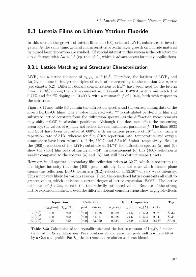
8.3 Lutetia Films on Lithium Yttrium Fluoride
8.3 Lutetia Films on Lithium Yttrium Fluoride
In this section the growth of lutetia films on 〈100〉 oriented LiYF4 substrates is investi-gated. At the same time, general characteristics of oxidic layer growth on fluoride materialby pulsed laser deposition are studied. Of special interest in this system is the refractive in-dex difference with ∆n ≈ 0.5 (cp. table 5.2), which is advantageous for many applications.
8.3.1 Lattice Matching and Structural Characterization
LiYF4 has a lattice constant of aLiYF4= 5.16 A. Therefore, the lattices of LiYF4 and
Lu2O3 combine in integer multiples of each other according to the relation 2 × as≈ af(cp. chapter 5.2). Different dopant concentrations of Eu3+ have been used for the lutetiafilms. For 8% doping the lattice constant would result in 10.428 A, with a mismatch f of0.77% and for 2% doping in 10.400 A with a mismatch f of 1.04%, both with respect tothe substrate.
Figure 8.15 and table 8.3 contain the diffraction spectra and the corresponding data of thegrown Eu:Lu2O3 films. The f value indicated with ‘*’ is calculated by deriving film andsubstrate lattice constant from the diffraction spectra, as the diffraction measurementsmay shift ± 0.05 � in absolute positions. Although this does not affect the measuringaccuracy, the values of a⊥ may not reflect the real mismatch parameter f . The films S033and S034 have been deposited at 600 � C with an oxygen pressure of 10−2mbar using arepetition rate of 3Hz, whereas for film SR09 repetition rate, temperature and oxygenatmosphere have been reduced to 1Hz, 550 � C and 5.5×10⁻³mbar, respectively. Besidesthe {200} reflection of the LiYF4 substrate at 34.74 � the diffraction spectra (a) and (b)show the {400} film peak of Lu2O3 at ≈34 � . In measurement (c) this {400} reflection isweaker compared to the spectra (a) and (b), but still has distinct shape (inset).
However, in all spectra a secondary film reflection arises at 32.7 � , which in spectrum (c)has higher intensity than the {400} peak. Initially, it is not clear which atomic planecauses this reflection. Lu2O3 features a {312} reflection at 32.207 � of very weak intensity.This is not very likely for various reasons. First, the considered lattice constants all shift togreater values, which indicates a certain degree of lattice expansion [Bal67]. The latticemismatch of f > 2%, exceeds the theoretically estimated value. Because of the stronglattice expansion influence, even the different dopant concentrations show negligible effects
Deposition Reflection Film Properties Tag
dfilm(nm) Tsub( � C) peak 2θ(deg) bm(deg) L⊥(nm) a⊥(A) f(%)
Eu(8%) 100 600 {400} 34.018 0.379 24.5 10.533 2.02 S033Eu(2%) 100 600 {400} 34.011 0.378 24.6 10.535 2.04 S034Eu(2%) 70 550 {400} 33.920 0.334 27.9 10.563 2.13* SR09
Table 8.3: Calculation of the crystallite size and the lattice constant of Lu2O3 films de-termined by X-ray diffraction. Peak positions 2θ and measured peak widths bm are fittedby a Gaussian profile. For L⊥ the instrumental resolution ba is considered.
107
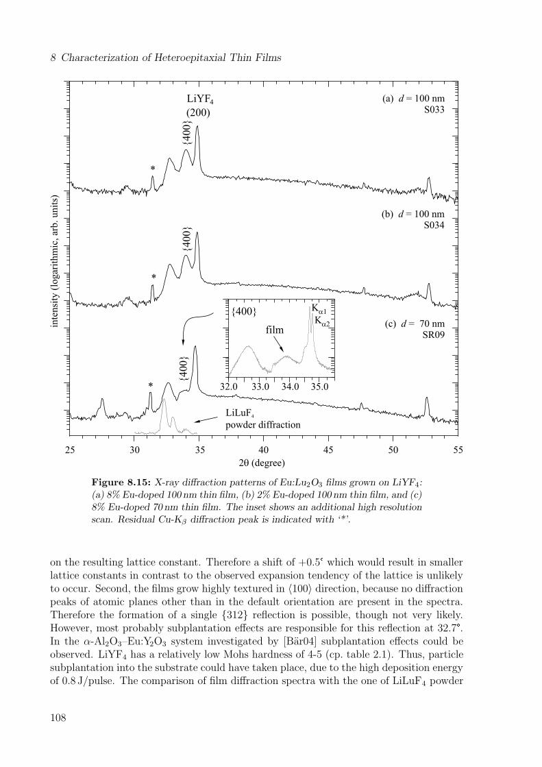
8 Characterization of Heteroepitaxial Thin Filmsin
ten
sity
(lo
gar
ith
mic
, ar
b.
un
its)
*
(a) = 100 nmS033
d
(b) = 100 nmS034
d
(c) = 70 nmSR09
d
{400}
{400}
{400}
*
*
25 30 35 40 45 5550
2 (degree)q
32.0 33.0 34.0 35.0
Ka2
Ka1
film
LiYF4
(200)
{400}
LiLuF4
powder diffraction
Figure 8.15: X-ray diffraction patterns of Eu:Lu2O3 films grown on LiYF4:(a) 8% Eu-doped 100 nm thin film, (b) 2% Eu-doped 100 nm thin film, and (c)8% Eu-doped 70 nm thin film. The inset shows an additional high resolutionscan. Residual Cu-Kβ diffraction peak is indicated with ‘*’.
on the resulting lattice constant. Therefore a shift of +0.5 � which would result in smallerlattice constants in contrast to the observed expansion tendency of the lattice is unlikelyto occur. Second, the films grow highly textured in 〈100〉 direction, because no diffractionpeaks of atomic planes other than in the default orientation are present in the spectra.Therefore the formation of a single {312} reflection is possible, though not very likely.However, most probably subplantation effects are responsible for this reflection at 32.7 � .In the α-Al2O3–Eu:Y2O3 system investigated by [Bar04] subplantation effects could beobserved. LiYF4 has a relatively low Mohs hardness of 4-5 (cp. table 2.1). Thus, particlesubplantation into the substrate could have taken place, due to the high deposition energyof 0.8 J/pulse. The comparison of film diffraction spectra with the one of LiLuF4 powder
108
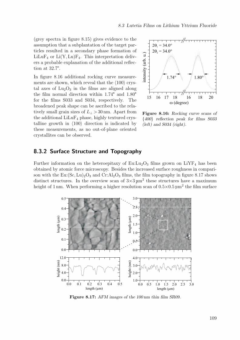
8.3 Lutetia Films on Lithium Yttrium Fluoride
inte
nsi
ty (
arb
. u
.)
w (degree)
15 16 17 18 16
1.74° 1.80°
2 = 34.0°q1
2 = 34.0°q2
18 20
Figure 8.16: Rocking curve scans of{400} reflection peak for films S033(left) and S034 (right).
(grey spectra in figure 8.15) gives evidence to theassumption that a subplantation of the target par-ticles resulted in a secondary phase formation ofLiLuF4 or Li(Y, Lu)F4. This interpretation deliv-ers a probable explanation of the additional reflec-tion at 32.7 � .
In figure 8.16 additional rocking curve measure-ments are shown, which reveal that the 〈100〉 crys-tal axes of Lu2O3 in the films are aligned alongthe film normal direction within 1.74 � and 1.80 �for the films S033 and S034, respectively. Thebroadened peak shape can be ascribed to the rela-tively small grain sizes of L⊥> 30 nm. Apart fromthe additional LiLuF4 phase, highly textured crys-talline growth in 〈100〉 direction is indicated bythese measurements, as no out-of-plane orientedcrystallites can be observed.
8.3.2 Surface Structure and Topography
Further information on the heteroepitaxy of Eu:Lu2O3 films grown on LiYF4 has beenobtained by atomic force microscopy. Besides the increased surface roughness in compari-son with the Eu:(Sc, Lu)2O3 and Cr:Al2O3 films, the film topography in figure 8.17 showsdistinct structures. In the overview scan of 3×3 � m2 these structures have a maximumheight of 1 nm. When performing a higher resolution scan of 0.5×0.5 � m2 the film surface
0.0 0.1 0.2 0.3 0.4 0.50.0
4.0
8.0
12.0
0.0
0.1
0.2
0.3
0.4
length (µm)
hei
gh
t (n
m)
len
gth
(µ
m)
0.5
0.0 0.5 1.0 1.5 2.0 3.01.0
2.0
3.0
4.0
0.0
0.5
1.0
1.5
2.0
3.0
length (µm)
hei
gh
t (n
m)
len
gth
(µ
m)
2.5
2.5
Figure 8.17: AFM images of the 100 nm thin film SR09.
109
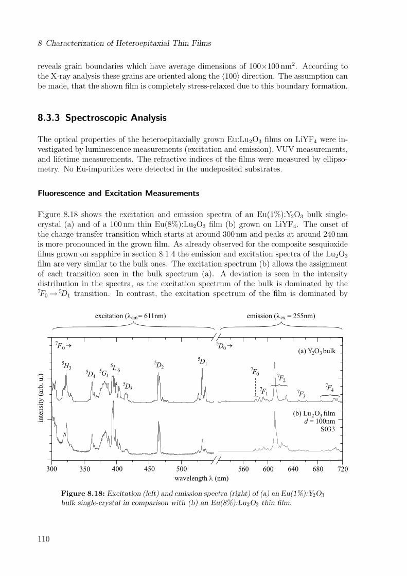
8 Characterization of Heteroepitaxial Thin Films
reveals grain boundaries which have average dimensions of 100×100 nm2. According tothe X-ray analysis these grains are oriented along the 〈100〉 direction. The assumption canbe made, that the shown film is completely stress-relaxed due to this boundary formation.
8.3.3 Spectroscopic Analysis
The optical properties of the heteroepitaxially grown Eu:Lu2O3 films on LiYF4 were in-vestigated by luminescence measurements (excitation and emission), VUV measurements,and lifetime measurements. The refractive indices of the films were measured by ellipso-metry. No Eu-impurities were detected in the undeposited substrates.
Fluorescence and Excitation Measurements
Figure 8.18 shows the excitation and emission spectra of an Eu(1%):Y2O3 bulk single-crystal (a) and of a 100 nm thin Eu(8%):Lu2O3 film (b) grown on LiYF4. The onset ofthe charge transfer transition which starts at around 300 nm and peaks at around 240 nmis more pronounced in the grown film. As already observed for the composite sesquioxidefilms grown on sapphire in section 8.1.4 the emission and excitation spectra of the Lu2O3
film are very similar to the bulk ones. The excitation spectrum (b) allows the assignmentof each transition seen in the bulk spectrum (a). A deviation is seen in the intensitydistribution in the spectra, as the excitation spectrum of the bulk is dominated by the7F0→ 5D1 transition. In contrast, the excitation spectrum of the film is dominated by
wavelength (nm)l
300 350 400 450 600 640 680 720
inte
nsi
ty (
arb
. u
.)
excitation ( = 611nm)lem emission ( = 255nm)lex
560
5D1
7F0
5D2
5D3
5L 65
GJ5D4
5H3
500
7F2
®5D0
7F3
7F4
®7F0
7F1
(a) Y O bulk2 3
(b) Lu= 100nm
S033d
O film2 3
Figure 8.18: Excitation (left) and emission spectra (right) of (a) an Eu(1%):Y2O3
bulk single-crystal in comparison with (b) an Eu(8%):Lu2O3 thin film.
110
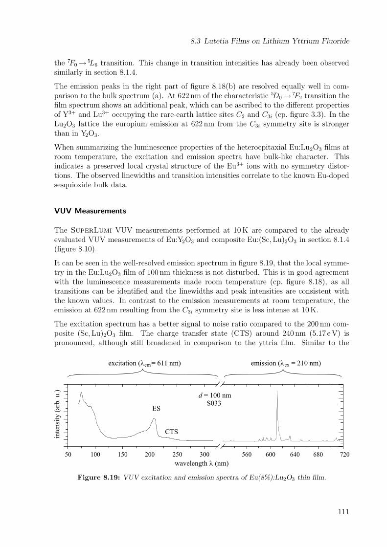
8.3 Lutetia Films on Lithium Yttrium Fluoride
the 7F0→ 5L6 transition. This change in transition intensities has already been observedsimilarly in section 8.1.4.
The emission peaks in the right part of figure 8.18(b) are resolved equally well in com-parison to the bulk spectrum (a). At 622 nm of the characteristic 5D0→ 7F2 transition thefilm spectrum shows an additional peak, which can be ascribed to the different propertiesof Y3+ and Lu3+ occupying the rare-earth lattice sites C2 and C3i (cp. figure 3.3). In theLu2O3 lattice the europium emission at 622 nm from the C3i symmetry site is strongerthan in Y2O3.
When summarizing the luminescence properties of the heteroepitaxial Eu:Lu2O3 films atroom temperature, the excitation and emission spectra have bulk-like character. Thisindicates a preserved local crystal structure of the Eu3+ ions with no symmetry distor-tions. The observed linewidths and transition intensities correlate to the known Eu-dopedsesquioxide bulk data.
VUV Measurements
The SuperLumi VUV measurements performed at 10K are compared to the alreadyevaluated VUV measurements of Eu:Y2O3 and composite Eu:(Sc, Lu)2O3 in section 8.1.4(figure 8.10).
It can be seen in the well-resolved emission spectrum in figure 8.19, that the local symme-try in the Eu:Lu2O3 film of 100 nm thickness is not disturbed. This is in good agreementwith the luminescence measurements made room temperature (cp. figure 8.18), as alltransitions can be identified and the linewidths and peak intensities are consistent withthe known values. In contrast to the emission measurements at room temperature, theemission at 622 nm resulting from the C3i symmetry site is less intense at 10K.
The excitation spectrum has a better signal to noise ratio compared to the 200 nm com-posite (Sc, Lu)2O3 film. The charge transfer state (CTS) around 240 nm (5.17 eV) ispronounced, although still broadened in comparison to the yttria film. Similar to the
50 100 150 200 250 300 560 600 640 720
wavelength (nm)l
inte
nsi
ty (
arb. u.)
excitation ( = 611 nm)lem emission ( = 210 nm)lex
ES
CTS
680
= 100 nm
S033
d
Figure 8.19: VUV excitation and emission spectra of Eu(8%):Lu2O3 thin film.
111
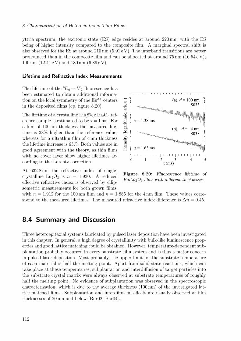
8 Characterization of Heteroepitaxial Thin Films
yttria spectrum, the excitonic state (ES) edge resides at around 220 nm, with the ESbeing of higher intensity compared to the composite film. A marginal spectral shift isalso observed for the ES at around 210 nm (5.91 eV). The interband transitions are betterpronounced than in the composite film and can be allocated at around 75 nm (16.54 eV),100 nm (12.41 eV) and 180 nm (6.89 eV).
Lifetime and Refractive Index Measurements
0 1 4 52 3t (ms)
inte
nsi
ty (
log
arit
hm
ic,
arb
. u
.)ô = 1.38 ms
(a) = 100 nmS033
d
(b) = 4 nmS038
d
ô = 1.63 ms
Figure 8.20: Fluorescence lifetime ofEu:Lu2O3 films with different thicknesses.
The lifetime of the 5D0→ 7F2 fluorescence hasbeen estimated to obtain additional informa-tion on the local symmetry of the Eu3+ centersin the deposited films (cp. figure 8.20).
The lifetime of a crystalline Eu(8%):Lu2O3 ref-erence sample is estimated to be τ =1ms. Fora film of 100 nm thickness the measured life-time is 38% higher than the reference value,whereas for a ultrathin film of 4 nm thicknessthe lifetime increase is 63%. Both values are ingood agreement with the theory, as thin filmswith no cover layer show higher lifetimes ac-cording to the Lorentz correction.
At 632.8 nm the refractive index of single-crystalline Lu2O3 is n = 1.930. A reducedeffective refractive index is observed by ellip-sometric measurements for both grown films,with n = 1.912 for the 100 nm film and n = 1.885 for the 4 nm film. These values corre-spond to the measured lifetimes. The measured refractive index difference is ∆n = 0.45.
8.4 Summary and Discussion
Three heteroepitaxial systems fabricated by pulsed laser deposition have been investigatedin this chapter. In general, a high degree of crystallinity with bulk-like luminescence prop-erties and good lattice matching could be obtained. However, temperature-dependent sub-plantation probably occurred in every substrate–film system and is thus a major concernin pulsed laser deposition. Most probably, the upper limit for the substrate temperatureof each material is half the melting point. Apart from solid-state reactions, which cantake place at these temperatures, subplantation and interdiffusion of target particles intothe substrate crystal matrix were always observed at substrate temperatures of roughlyhalf the melting point. No evidence of subplantation was observed in the spectroscopiccharacterization, which is due to the average thickness (100 nm) of the investigated lat-tice matched films. Subplantation and interdiffusion effects are usually observed at filmthicknesses of 20 nm and below [Bur02, Bar04].
112
8.4 Summary and Discussion
Composite Sesquioxide Films on Sapphire
The growth on sapphire substrates requires high temperatures. Although highly tex-tured crystalline films can be obtained at temperatures of 700 � C, better film propertiesare achievable at higher deposition temperatures. An indicator thereof is the crystallitesize which almost reaches the estimated film thickness for temperatures above 1000 � C.For lower deposition temperatures the distribution of [111] oriented, but relatively smallcrystallites result in broad rocking curves as seen in figure 8.3. However, at tempera-tures above 800 � C the deposited films reveal subplantation effects, which most probablyresulted in the formation of a second perovskite phase as already observed for the Al2O3–Eu:Y2O3 films by S. Bar [Bar04]. Despite the high Mohs hardness of α-Al2O3, the highreactivity of Al3+ might contribute to the formation of new phases by subplantation. Theadditional diffraction peaks have been interpreted as [100] (Sc, Lu)AlO3. These subplan-tation effects at higher temperatures have to be suppressed by the deposition parameters,e. g. by gradually reducing the pulse energy in a series of films to estimate a possiblecompromise between pulse energies required for single-crystalline deposition and pulseenergies resulting in undesired subplantation effects.
Additional RHEED analysis revealed the formation of an amorphous interface at initialgrowth, which prevents a sustaining layer-by-layer growth on α-Al2O3. This has alsobeen observed in the pulsed laser deposition of Al2O3–Sc2O3 films [Gun07]. Thus, furtherdeposition attempts on sapphire substrates should include a buffer layer in order to preventthe initial growth of an amorphous interface and thereby realize layer-by-layer grown films.
By pre-deposition substrate treatment the surface roughness of the grown films is stronglyreduced in comparison to untreated substrates [Bar04, Han07]. Further investigationsregarding the in-plane characteristics of the film lattice are to be done by surface X-raydiffraction measurements.
A lattice matching of up to 99.88% could be obtained by composition [2] with luminescenceproperties similar to bulk single-crystals. It is difficult to assess whether the mismatch of0.12% is caused by lattice expansion in the grown film. Otherwise, composition [2] can beimproved by shifting the two-component mixture more to scandium while reducing thelutetia amount. However, the used compositions fit the estimation quite well and onlyfine-tuning has to be done. For laser applications the Eu3+ dopant could be replaced byYb3+ or Er3+ ions, which would also result in a more homogenous lattice as the ionic radiiof both laser ions are closer to the ones of Sc3+ and Lu3+. The measured refractive indexdifference of ∆n = 0.2 at wavelengths of 632.8 nm recommend this system for waveguidingapplications.
Sapphire Films on Composite Sesquioxide
A major issue of the growth on composite sesquioxides is the substrate quality. The 〈111〉oriented ScLuO3 substrates contained various rare-earth impurities such as holmium,praseodymium, and erbium, which appeared in the luminescence measurements. Thisproblem is a well-known characteristic of lanthanides, which can only be separated and
113
8 Characterization of Heteroepitaxial Thin Films
isolated to a certain degree. In the case of two lanthanide compounds as seed mate-rials the lanthanide impurity amount is almost doubled. However, the combination ofCr(0.5%):Al2O3 with ScLuO3 resulting in a theoretical lattice matching of 99.99% is awell-suited heteroepitaxial system for PLD.
Similar to the reverse substrate–film system, subplantation was observed at substratetemperatures of 950 � C. As solid solutions have reduced melting points due to bondingforce modifications in the crystal matrix, 950 � C was probably above half the meltingtemperature of (Sc, Lu)2O3. In addition, the material hardness of solid solutions is alsolikely to be reduced in comparison to the corresponding single-component material. Dueto these factors, most probably [111] (Sc, Lu)AlO3 was formed by subplantation andinterdiffusion of Al2O3 into the (Sc, Lu)2O3 matrix.
Apart from these difficulties, a highly crystalline film could be deposited at 700 � C with acrystallite size which goes beyond the Scherrer equation limits. The FWHM peak widthof the (0006) film reflection was similar to the substrate values, indicating monocrystallineepitaxial film growth. With this film a lattice matching of 99.46% was achieved. Furthergrowth of this promising systems will be performed at optimum temperatures around700 � C. As for this substrate–film system the lower refractive index is on the film-side, itwould be well-suited for application as Bragg mirrors and antireflex coatings.
Lutetia Films on Lithium Yttrium Fluoride
The combination of oxide and fluoride materials incorporates some difficulties. As de-scribed before, a certain oxygen pressure is required for the pulsed laser deposition ofoxidic materials. Due to this basic oxygen atmosphere, there is the danger of undesiredoxyfluoride formation during deposition, e. g. an amorphous oxyfluoride interface betweenfilm and substrate. Pre-deposition substrate treatment has to be done in argon or nitrogenatmosphere to prevent oxidation. However, it has not been possible to obtain atomicallyflat terraces by this treatment.
The subplantation and interdiffusion of Lu2O3 into the LiYF4 matrix probably cause aLi(Y, Lu)F4 phase in the deposited thin film. This is understood due to the relativelylow Mohs hardness of fluoride materials. Therefore, the deposition energy has to bereduced in further experiments in order to prevent subplantation and interdiffusion oftarget particles. Other parameter changes have to be considered regarding the substratetemperature and the oxygen pressure. In review, less optimal deposition parameters wereused for this substrate–film system, as only few information on the pulsed laser depositionof fluorides was available. Further research in this field has to be done in future.
Despite these complications, crystalline 〈100〉 oriented Eu:Lu2O3 films with bulk-like lu-minescence properties were obtained. The obtained lattice matching of 97.98% has anobservable degree of lattice expansion, as a shift to greater lattice constants than theoreti-cally calculated took place. This system is highly suited for optical applications regardingthe comparably high refractive index difference of ∆n = 0.45, provided that the growthdifficulties can be resolved in future.
114
9 Characterization of Homo- and
Quasi-Homoepitaxial Thin Films
The characterization of lattice matched homo- and quasi-homoepitaxial thin film sys-tems is subject of this chapter. Investigated materials are sesquioxides, orthovanadates,and aluminum garnets. In contrast to the heteroepitaxial systems, the lattices of sub-strate and film are very similar in homo- and quasi-homoepitaxy and combine directly(cp. chapter 5.2). Therefore, the epitaxy is energetically more favorable and better resultsare expected in regard of the film growth process and the resulting film quality.
In addition, heteroepitaxy with pulsed laser deposition may lead to subplantation effects,which disturb the growth process. In homo- and quasi-homoepitaxy the formation ofadditional phases due to subplantation, as observed in the previous chapter 8 for thedeposition of sesquioxides on α-Al2O3 and LiYF4 substrates, is unlikely to occur.
9.1 Sesquioxide Films on Yttria
In this section the properties of different sesquioxide films on yttria are studied. While inheteroepitaxy on sapphire only one growth direction could be investigated, the homo- andquasi-homoepitaxy will consider [111] and [100] sesquioxide films. In Eu:Y2O3 films theionic radius of Eu3+ is bigger than that of Y3+, thus the cation site in yttria is enlarged.This results in a slight lattice constant increase. The properties of these homoepitaxialfilms are compared to those of Eu:Lu2O3 films. The Lu3+ and Eu3+ ions effect the yttrialattice in compensating manner, as rLu3+ <rY3+ <rEu3+ (cp. table 9.1). At last, latticematching on yttria is achieved by the composite system Eu:(Gd, Lu)2O3.
9.1.1 Lattice Matching
In the above described cases of Eu:RE2O3 deposited on yttria the lattices combine directlyas≈ af (cp. chapter 5.2). Apart from the growth of homoepitaxial Eu:Y2O3 and quasi-homoepitaxial Eu:Lu2O3 films, both introducing a small lattice mismatch to yttria, it isof special interest to investigate a composite sesquioxide film to fit the substrate latticeconstant aY2O3
=10.603 A perfectly and obtain a higher refractive index difference as well.
As already done similarly for Eu:(Sc, Lu)2O3 films, a composition with 2% Eu-doping isdetermined by the Vegard law (equation 5.3) to be (Eu0.02Gd0.534Lu0.446)2O3 [1]. This
115
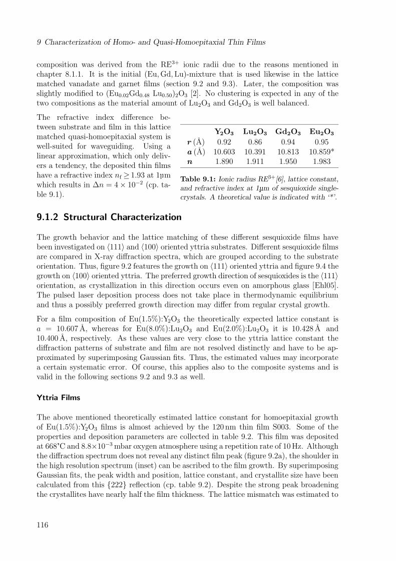
9 Characterization of Homo- and Quasi-Homoepitaxial Thin Films
composition was derived from the RE3+ ionic radii due to the reasons mentioned inchapter 8.1.1. It is the initial (Eu,Gd, Lu)-mixture that is used likewise in the latticematched vanadate and garnet films (section 9.2 and 9.3). Later, the composition wasslightly modified to (Eu0.02Gd0.48 Lu0.50)2O3 [2]. No clustering is expected in any of thetwo compositions as the material amount of Lu2O3 and Gd2O3 is well balanced.
Y2O3 Lu2O3 Gd2O3 Eu2O3
r (A) 0.92 0.86 0.94 0.95a (A) 10.603 10.391 10.813 10.859*n 1.890 1.911 1.950 1.983
Table 9.1: Ionic radius RE3+[6], lattice constant,and refractive index at 1� m of sesquioxide single-crystals. A theoretical value is indicated with ‘*’.
The refractive index difference be-tween substrate and film in this latticematched quasi-homoepitaxial system iswell-suited for waveguiding. Using alinear approximation, which only deliv-ers a tendency, the deposited thin filmshave a refractive index nf ≥ 1.93 at 1 � mwhich results in ∆n = 4× 10⁻² (cp. ta-ble 9.1).
9.1.2 Structural Characterization
The growth behavior and the lattice matching of these different sesquioxide films havebeen investigated on 〈111〉 and 〈100〉 oriented yttria substrates. Different sesquioxide filmsare compared in X-ray diffraction spectra, which are grouped according to the substrateorientation. Thus, figure 9.2 features the growth on 〈111〉 oriented yttria and figure 9.4 thegrowth on 〈100〉 oriented yttria. The preferred growth direction of sesquioxides is the 〈111〉orientation, as crystallization in this direction occurs even on amorphous glass [Ehl05].The pulsed laser deposition process does not take place in thermodynamic equilibriumand thus a possibly preferred growth direction may differ from regular crystal growth.
For a film composition of Eu(1.5%):Y2O3 the theoretically expected lattice constant isa = 10.607 A, whereas for Eu(8.0%):Lu2O3 and Eu(2.0%):Lu2O3 it is 10.428 A and10.400 A, respectively. As these values are very close to the yttria lattice constant thediffraction patterns of substrate and film are not resolved distinctly and have to be ap-proximated by superimposing Gaussian fits. Thus, the estimated values may incorporatea certain systematic error. Of course, this applies also to the composite systems and isvalid in the following sections 9.2 and 9.3 as well.
Yttria Films
The above mentioned theoretically estimated lattice constant for homoepitaxial growthof Eu(1.5%):Y2O3 films is almost achieved by the 120 nm thin film S003. Some of theproperties and deposition parameters are collected in table 9.2. This film was depositedat 668 � C and 8.8×10⁻³mbar oxygen atmosphere using a repetition rate of 10Hz. Althoughthe diffraction spectrum does not reveal any distinct film peak (figure 9.2a), the shoulder inthe high resolution spectrum (inset) can be ascribed to the film growth. By superimposingGaussian fits, the peak width and position, lattice constant, and crystallite size have beencalculated from this {222} reflection (cp. table 9.2). Despite the strong peak broadeningthe crystallites have nearly half the film thickness. The lattice mismatch was estimated to
116
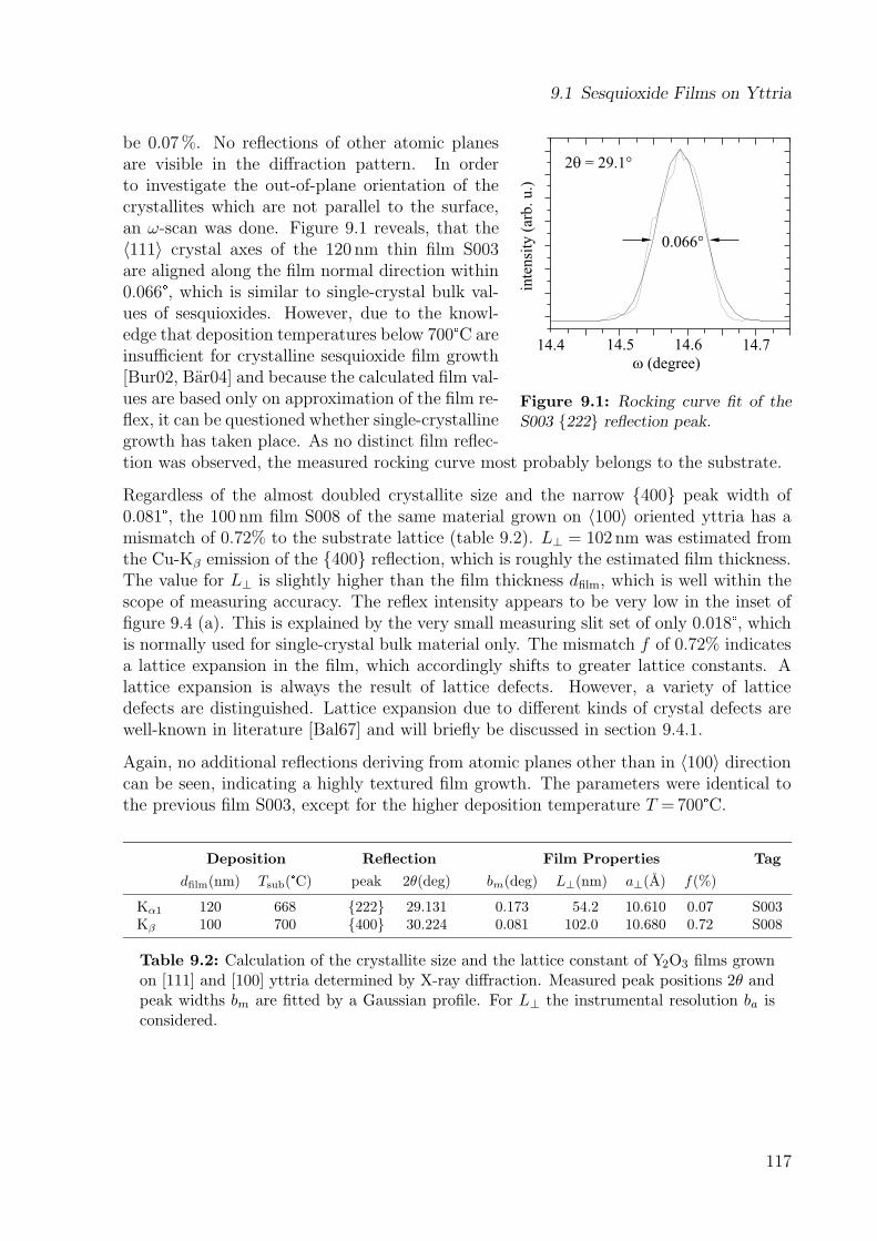
9.1 Sesquioxide Films on Yttria
inte
nsi
ty (
arb. u.)
14.4 14.5 14.6 14.7
w (degree)
0.066°
2 = 29.1°q
Figure 9.1: Rocking curve fit of theS003 {222} reflection peak.
be 0.07%. No reflections of other atomic planesare visible in the diffraction pattern. In orderto investigate the out-of-plane orientation of thecrystallites which are not parallel to the surface,an ω-scan was done. Figure 9.1 reveals, that the〈111〉 crystal axes of the 120 nm thin film S003are aligned along the film normal direction within0.066 � , which is similar to single-crystal bulk val-ues of sesquioxides. However, due to the knowl-edge that deposition temperatures below 700 � C areinsufficient for crystalline sesquioxide film growth[Bur02, Bar04] and because the calculated film val-ues are based only on approximation of the film re-flex, it can be questioned whether single-crystallinegrowth has taken place. As no distinct film reflec-tion was observed, the measured rocking curve most probably belongs to the substrate.
Regardless of the almost doubled crystallite size and the narrow {400} peak width of0.081 � , the 100 nm film S008 of the same material grown on 〈100〉 oriented yttria has amismatch of 0.72% to the substrate lattice (table 9.2). L⊥ = 102 nm was estimated fromthe Cu-Kβ emission of the {400} reflection, which is roughly the estimated film thickness.The value for L⊥ is slightly higher than the film thickness dfilm, which is well within thescope of measuring accuracy. The reflex intensity appears to be very low in the inset offigure 9.4 (a). This is explained by the very small measuring slit set of only 0.018 � , whichis normally used for single-crystal bulk material only. The mismatch f of 0.72% indicatesa lattice expansion in the film, which accordingly shifts to greater lattice constants. Alattice expansion is always the result of lattice defects. However, a variety of latticedefects are distinguished. Lattice expansion due to different kinds of crystal defects arewell-known in literature [Bal67] and will briefly be discussed in section 9.4.1.
Again, no additional reflections deriving from atomic planes other than in 〈100〉 directioncan be seen, indicating a highly textured film growth. The parameters were identical tothe previous film S003, except for the higher deposition temperature T =700 � C.
Deposition Reflection Film Properties Tag
dfilm(nm) Tsub( � C) peak 2θ(deg) bm(deg) L⊥(nm) a⊥(A) f(%)
Kα1 120 668 {222} 29.131 0.173 54.2 10.610 0.07 S003Kβ 100 700 {400} 30.224 0.081 102.0 10.680 0.72 S008
Table 9.2: Calculation of the crystallite size and the lattice constant of Y2O3 films grownon [111] and [100] yttria determined by X-ray diffraction. Measured peak positions 2θ andpeak widths bm are fitted by a Gaussian profile. For L⊥ the instrumental resolution ba isconsidered.
117
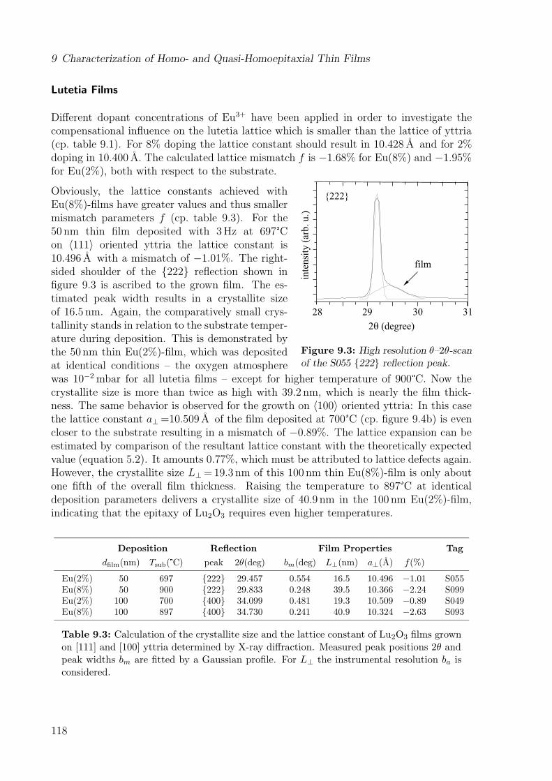
9 Characterization of Homo- and Quasi-Homoepitaxial Thin Films
Lutetia Films
Different dopant concentrations of Eu3+ have been applied in order to investigate thecompensational influence on the lutetia lattice which is smaller than the lattice of yttria(cp. table 9.1). For 8% doping the lattice constant should result in 10.428 A and for 2%doping in 10.400 A. The calculated lattice mismatch f is −1.68% for Eu(8%) and −1.95%
inte
nsi
ty (
arb. u.)
28 29 30 31
2q (degree)
{222}
film
Figure 9.3: High resolution θ–2θ-scanof the S055 {222} reflection peak.
for Eu(2%), both with respect to the substrate.
Obviously, the lattice constants achieved withEu(8%)-films have greater values and thus smallermismatch parameters f (cp. table 9.3). For the50 nm thin film deposited with 3Hz at 697 � Con 〈111〉 oriented yttria the lattice constant is10.496 A with a mismatch of −1.01%. The right-sided shoulder of the {222} reflection shown infigure 9.3 is ascribed to the grown film. The es-timated peak width results in a crystallite sizeof 16.5 nm. Again, the comparatively small crys-tallinity stands in relation to the substrate temper-ature during deposition. This is demonstrated bythe 50 nm thin Eu(2%)-film, which was depositedat identical conditions – the oxygen atmospherewas 10−2mbar for all lutetia films – except for higher temperature of 900 � C. Now thecrystallite size is more than twice as high with 39.2 nm, which is nearly the film thick-ness. The same behavior is observed for the growth on 〈100〉 oriented yttria: In this casethe lattice constant a⊥=10.509 A of the film deposited at 700 � C (cp. figure 9.4b) is evencloser to the substrate resulting in a mismatch of −0.89%. The lattice expansion can beestimated by comparison of the resultant lattice constant with the theoretically expectedvalue (equation 5.2). It amounts 0.77%, which must be attributed to lattice defects again.However, the crystallite size L⊥=19.3 nm of this 100 nm thin Eu(8%)-film is only aboutone fifth of the overall film thickness. Raising the temperature to 897 � C at identicaldeposition parameters delivers a crystallite size of 40.9 nm in the 100 nm Eu(2%)-film,indicating that the epitaxy of Lu2O3 requires even higher temperatures.
Deposition Reflection Film Properties Tag
dfilm(nm) Tsub( � C) peak 2θ(deg) bm(deg) L⊥(nm) a⊥(A) f(%)
Eu(2%) 50 697 {222} 29.457 0.554 16.5 10.496 −1.01 S055Eu(8%) 50 900 {222} 29.833 0.248 39.5 10.366 −2.24 S099Eu(2%) 100 700 {400} 34.099 0.481 19.3 10.509 −0.89 S049Eu(8%) 100 897 {400} 34.730 0.241 40.9 10.324 −2.63 S093
Table 9.3: Calculation of the crystallite size and the lattice constant of Lu2O3 films grownon [111] and [100] yttria determined by X-ray diffraction. Measured peak positions 2θ andpeak widths bm are fitted by a Gaussian profile. For L⊥ the instrumental resolution ba isconsidered.
118
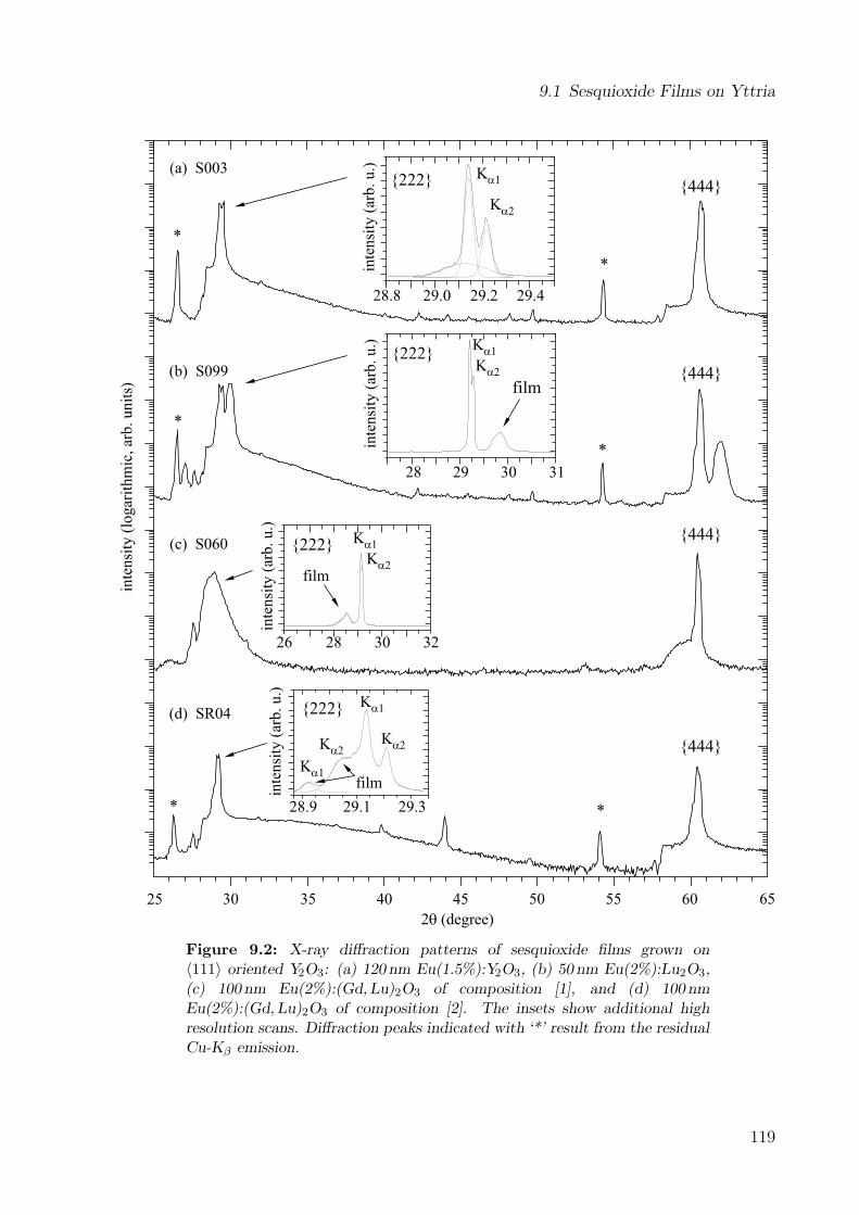
9.1 Sesquioxide Films on Yttria
25 30 35 40 45 55 60 6550
2 (degree)q
inte
nsi
ty (
logar
ithm
ic, ar
b. unit
s)
*
(a) S003
(b) S099
(c) S060
(d) SR04
*
*
{444}
{444}
*
*
*
{222}
inte
nsi
ty (
arb. u.)
28.8 29.0 29.2 29.4
Ka2
Ka1
{222}in
tensi
ty (
arb. u.)
28 29 30 31
Ka2
Ka1
film{444}
{222}
inte
nsi
ty (
arb. u.)
26 28 30 32
Ka2
Ka1
film
{222}
inte
nsi
ty (
arb. u.)
28.9 29.329.1
Ka2
Ka1
filmK
a1
Ka2
{444}
Figure 9.2: X-ray diffraction patterns of sesquioxide films grown on〈111〉 oriented Y2O3: (a) 120 nm Eu(1.5%):Y2O3, (b) 50 nm Eu(2%):Lu2O3,(c) 100 nm Eu(2%):(Gd, Lu)2O3 of composition [1], and (d) 100 nmEu(2%):(Gd, Lu)2O3 of composition [2]. The insets show additional highresolution scans. Diffraction peaks indicated with ‘*’ result from the residualCu-Kβ emission.
119
9 Characterization of Homo- and Quasi-Homoepitaxial Thin Films
Regarding the expected lattice constant for Eu(2%) doping, in both orientations the ex-perimental values match very well within the measuring accuracy. Due to the highertemperature in both depositions, the crystallinity and peak width of both films are com-parable in value. As no additional reflections from atomic planes other than in the defaultsubstrate direction are visible in the diffraction spectra, both films indicate highly tex-tured crystalline growth in the substrate orientation: the 50 nm thin film in 〈111〉 direction(cp. figure 9.2b) and the 100 nm thin film in 〈100〉 direction (cp. figure 9.4c). The fact,that the film lattice constants match well with the theoretically calculated values can havedifferent reasons. First, the lower Eu3+ doping in both films results in a better compen-sation in the lutetia lattice. It is possible, that a concentration of 2% does not disturbthe lutetia lattice in a way, which would cause a lattice expansion. If the main part ofthe atomic plane distances diffracted by X-rays originate from undoped material due tostatistically distributed europium ions throughout the lattice, a local lattice disturbancedue to a single dopant ion will be of no consequence for the averaged diffraction pattern.Another explanation takes into account the higher deposition temperature for both lowerdoped films. A higher substrate temperature which increases the mobility of the depositedatoms can thereby amplify the ability of the lutetia lattice to compensate lower dopantconcentrations without a lattice expansion. However, in both films S093 and S099 theGaussian fit of the film reflection matches the diffraction pattern accurately and gives noevidence of a peak broadening.
No preferred film growth direction can be derived from the analyzed films. Although themeasured lattice constants of the films grown in 〈111〉 direction are closer to the calculatedvalues, this also can be ascribed to the film thickness. It was observed that the diffractionpeaks of films with thicknesses of≤ 50 nm shift to smaller angles (greater lattice constants)with further increasing thickness. Therefore, the reflection peaks of these thinner filmsmay not be entirely pronounced and change their 2θ-position to smaller angles at higherthickness [Bur02, Bar04]. This behavior would relativize the above mentioned observation.
Composite Sesquioxide Films
Four composite sesquioxide films are compared, each of 100 nm thickness. Apart fromthe film S060, all films have been deposited at high substrate temperatures T ≥ 900 � Cand an oxygen atmosphere of 8.9 – 9.0×10⁻³mbar using a repetition rate of 1Hz. Onlyfor the film SR11 the oxygen atmosphere had to be reduced to 4.6×10⁻³mbar as theobtained RHEED diffraction images were too weak. As summarized in table 9.4 the filmof composition [1] achieves a lattice constant of a⊥ = 10.818 A which misses the substratelattice constant by f = 1.99% (cp. figure 9.2c). It was deposited at 702 � C and theestimated crystallite size L⊥=26.8 nm is roughly one fourth of the film thickness. Peakbroadening is observed due to lattice expansion which is also caused by the mismatch f .
Despite the identical composition [2] and the similar deposition parameters a certainmismatch with respect to the substrate remains for all films. The f values in table 9.4indicated with ‘*’ are calculated by deriving film and substrate lattice constant fromthe diffraction spectra, as these diffraction measurements show a variation of ± 0.05 �in absolute positions. Therefore the values of a⊥ may not reflect the real mismatch
120
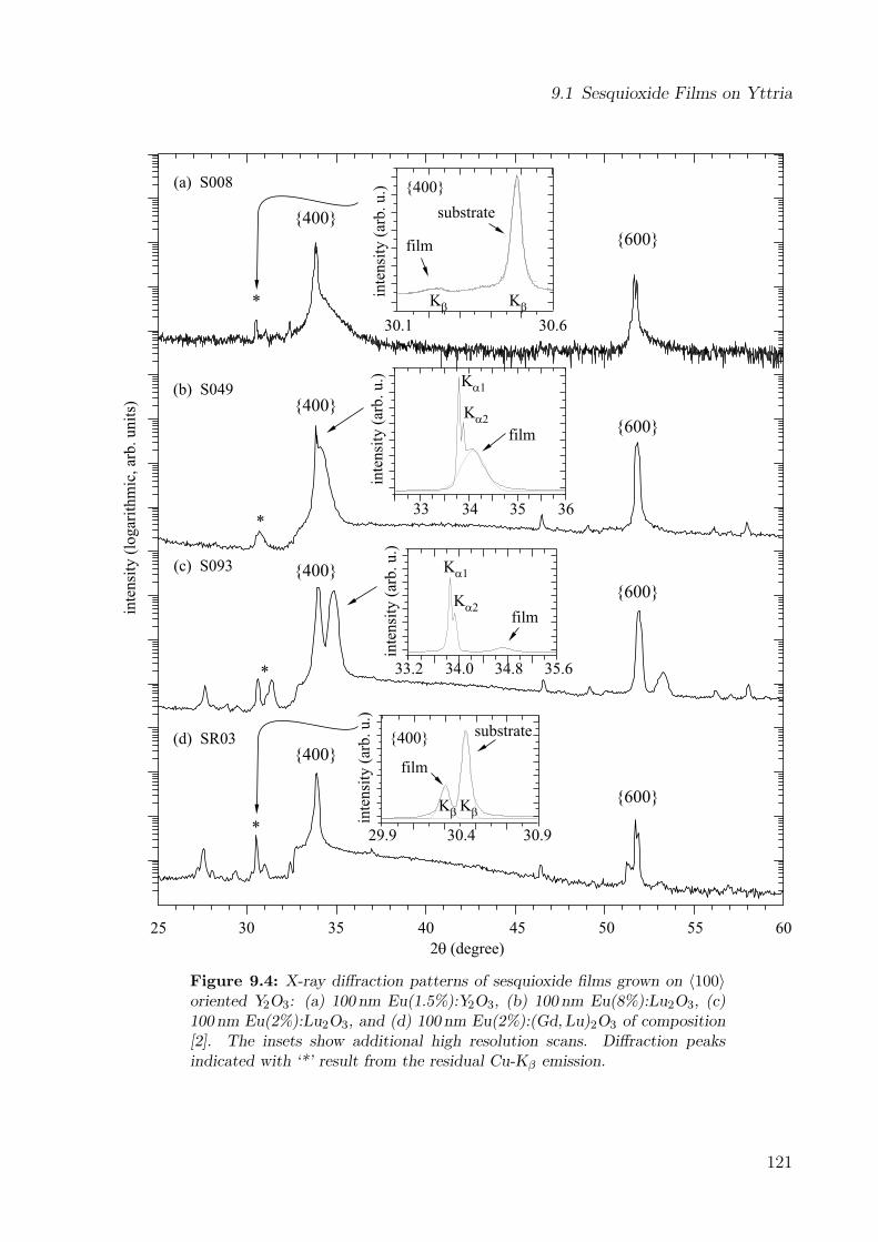
9.1 Sesquioxide Films on Yttria
25 30 35 40 45 55 6050
2 (degree)q
inte
nsi
ty (
logar
ithm
ic, ar
b. unit
s)
(a) S008
(b) S049
(c) S093
(d) SR03
*
{400}
{400}
*
{400}
{400}
30.6
{400}
film
inte
nsi
ty (
arb. u.)
30.1
KbKb
substrate
inte
nsi
ty (
arb. u.)
33 34 35 36
Ka2
Ka1
film
inte
nsi
ty (
arb. u.)
33.2 34.0 34.8 35.6
Ka2
Ka1
film
inte
nsi
ty (
arb. u.)
29.9 30.4 30.9
film
substrate
KbKb
{600}
{600}
{600}
{600}
*
*
{400}
Figure 9.4: X-ray diffraction patterns of sesquioxide films grown on 〈100〉oriented Y2O3: (a) 100 nm Eu(1.5%):Y2O3, (b) 100 nm Eu(8%):Lu2O3, (c)100 nm Eu(2%):Lu2O3, and (d) 100 nm Eu(2%):(Gd, Lu)2O3 of composition[2]. The insets show additional high resolution scans. Diffraction peaksindicated with ‘*’ result from the residual Cu-Kβ emission.
121
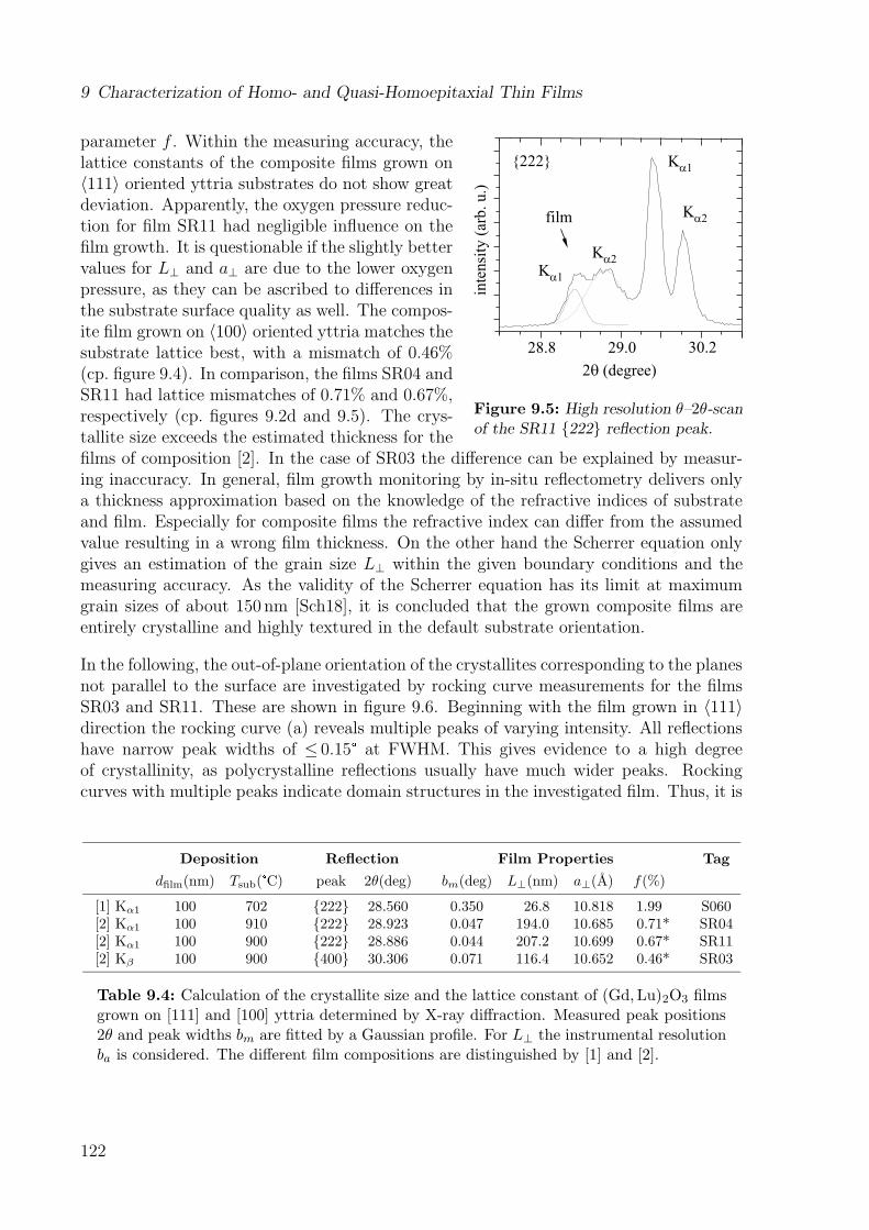
9 Characterization of Homo- and Quasi-Homoepitaxial Thin Films
inte
nsi
ty (
arb. u.)
28.8 29.0 30.2
2q (degree)
{222}
Ka2
Ka1
film
Ka2
Ka1
Figure 9.5: High resolution θ–2θ-scanof the SR11 {222} reflection peak.
parameter f . Within the measuring accuracy, thelattice constants of the composite films grown on〈111〉 oriented yttria substrates do not show greatdeviation. Apparently, the oxygen pressure reduc-tion for film SR11 had negligible influence on thefilm growth. It is questionable if the slightly bettervalues for L⊥ and a⊥ are due to the lower oxygenpressure, as they can be ascribed to differences inthe substrate surface quality as well. The compos-ite film grown on 〈100〉 oriented yttria matches thesubstrate lattice best, with a mismatch of 0.46%(cp. figure 9.4). In comparison, the films SR04 andSR11 had lattice mismatches of 0.71% and 0.67%,respectively (cp. figures 9.2d and 9.5). The crys-tallite size exceeds the estimated thickness for thefilms of composition [2]. In the case of SR03 the difference can be explained by measur-ing inaccuracy. In general, film growth monitoring by in-situ reflectometry delivers onlya thickness approximation based on the knowledge of the refractive indices of substrateand film. Especially for composite films the refractive index can differ from the assumedvalue resulting in a wrong film thickness. On the other hand the Scherrer equation onlygives an estimation of the grain size L⊥ within the given boundary conditions and themeasuring accuracy. As the validity of the Scherrer equation has its limit at maximumgrain sizes of about 150 nm [Sch18], it is concluded that the grown composite films areentirely crystalline and highly textured in the default substrate orientation.
In the following, the out-of-plane orientation of the crystallites corresponding to the planesnot parallel to the surface are investigated by rocking curve measurements for the filmsSR03 and SR11. These are shown in figure 9.6. Beginning with the film grown in 〈111〉direction the rocking curve (a) reveals multiple peaks of varying intensity. All reflectionshave narrow peak widths of ≤ 0.15 � at FWHM. This gives evidence to a high degreeof crystallinity, as polycrystalline reflections usually have much wider peaks. Rockingcurves with multiple peaks indicate domain structures in the investigated film. Thus, it is
Deposition Reflection Film Properties Tag
dfilm(nm) Tsub( � C) peak 2θ(deg) bm(deg) L⊥(nm) a⊥(A) f(%)
[1] Kα1 100 702 {222} 28.560 0.350 26.8 10.818 1.99 S060[2] Kα1 100 910 {222} 28.923 0.047 194.0 10.685 0.71* SR04[2] Kα1 100 900 {222} 28.886 0.044 207.2 10.699 0.67* SR11[2] Kβ 100 900 {400} 30.306 0.071 116.4 10.652 0.46* SR03
Table 9.4: Calculation of the crystallite size and the lattice constant of (Gd, Lu)2O3 filmsgrown on [111] and [100] yttria determined by X-ray diffraction. Measured peak positions2θ and peak widths bm are fitted by a Gaussian profile. For L⊥ the instrumental resolutionba is considered. The different film compositions are distinguished by [1] and [2].
122
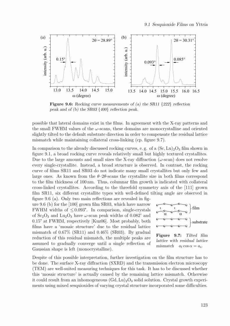
9.1 Sesquioxide Films on Yttria
inte
nsi
ty (
arb
. u
.)
14.0 15.0 16.0w (degree)
0.093°
2 = 30.31°q
0.085°
13.5 14.5 15.5 16.5
inte
nsi
ty (
arb
. u
.)
13.0 14.0 15.0
2 = 28.89°q
w (degree)
13.5 14.5
(a) (b)
0.15°
Figure 9.6: Rocking curve measurements of (a) the SR11 {222} reflectionpeak and of (b) the SR03 {400} reflection peak.
possible that lateral domains exist in the films. In agreement with the X-ray patterns andthe small FWHM values of the ω-scans, these domains are monocrystalline and orientedslightly tilted to the default substrate direction in order to compensate the residual latticemismatch while maintaining collateral cross-linking (cp. figure 9.7).
In comparison to the already discussed rocking curves, e. g. of a (Sc, Lu)2O3 film shown infigure 9.1, a broad rocking curve reveals relatively small but highly textured crystallites.Due to the large amounts and small sizes the X-ray diffraction (ω-scan) does not resolveevery single-crystallite. Instead, a broad structure is observed. In contrast, the rockingcurve of films SR11 and SR03 do not indicate many small crystallites but only few andlarge ones. As known from the θ–2θ-scans the crystallite size in both films correspondto the film thickness of 100 nm. Thus, columnar film growth is indicated with collateralcross-linked crystallites. According to the threefold symmetry axis of the [111] grownfilm SR11, six different crystallite types with well-defined tilting angle are observed in
a a
film
substrate
Figure 9.7: Tilted filmlattice with residual latticemismatch af cosα = as.
figure 9.6 (a). Only two main reflections are revealed in fig-ure 9.6 (b) for the [100] grown film SR03, which have narrowFWHM widths of ≤ 0.093 � . In comparison, single-crystalsof Sc2O3 and Lu2O3 have ω-scan peak widths of 0.082 � and0.15 � at FWHM, respectively [Kuz06]. Most probably, bothfilms have a ‘mosaic structure’ due to the residual latticemismatch of 0.67% (SR11) and 0.46% (SR03). By gradualreduction of this residual mismatch, the multiple peaks areassumed to gradually converge until a single reflection ofGaussian shape is left (monocrystalline).
Despite of this possible interpretation, further investigation on the film structure has tobe done. The surface X-ray diffraction (SXRD) and the transmission electron microscopy(TEM) are well-suited measuring techniques for this task. It has to be discussed whetherthis ‘mosaic structure’ is actually caused by the remaining lattice mismatch. Otherwiseit could result from an inhomogeneous (Gd, Lu)2O3 solid solution. Crystal growth experi-ments using mixed sesquioxides of varying crystal structure incorporated some difficulties.
123
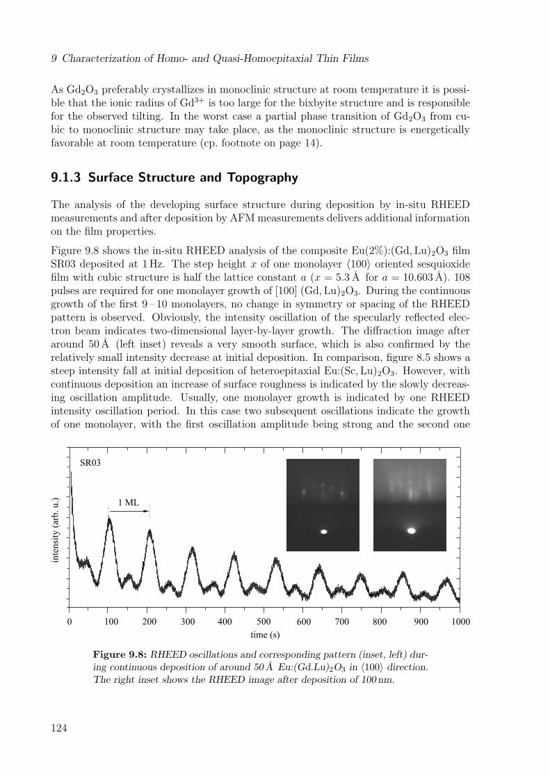
9 Characterization of Homo- and Quasi-Homoepitaxial Thin Films
As Gd2O3 preferably crystallizes in monoclinic structure at room temperature it is possi-ble that the ionic radius of Gd3+ is too large for the bixbyite structure and is responsiblefor the observed tilting. In the worst case a partial phase transition of Gd2O3 from cu-bic to monoclinic structure may take place, as the monoclinic structure is energeticallyfavorable at room temperature (cp. footnote on page 14).
9.1.3 Surface Structure and Topography
The analysis of the developing surface structure during deposition by in-situ RHEEDmeasurements and after deposition by AFM measurements delivers additional informationon the film properties.
Figure 9.8 shows the in-situ RHEED analysis of the composite Eu(2%):(Gd, Lu)2O3 filmSR03 deposited at 1Hz. The step height x of one monolayer 〈100〉 oriented sesquioxidefilm with cubic structure is half the lattice constant a (x = 5.3 A for a = 10.603 A). 108pulses are required for one monolayer growth of [100] (Gd, Lu)2O3. During the continuousgrowth of the first 9 – 10 monolayers, no change in symmetry or spacing of the RHEEDpattern is observed. Obviously, the intensity oscillation of the specularly reflected elec-tron beam indicates two-dimensional layer-by-layer growth. The diffraction image afteraround 50 A (left inset) reveals a very smooth surface, which is also confirmed by therelatively small intensity decrease at initial deposition. In comparison, figure 8.5 shows asteep intensity fall at initial deposition of heteroepitaxial Eu:(Sc, Lu)2O3. However, withcontinuous deposition an increase of surface roughness is indicated by the slowly decreas-ing oscillation amplitude. Usually, one monolayer growth is indicated by one RHEEDintensity oscillation period. In this case two subsequent oscillations indicate the growthof one monolayer, with the first oscillation amplitude being strong and the second one
inte
nsi
ty (
arb. u.)
0 100 200 300 400 600 700500
time (s)
800 900 1000
1 ML
SR03
Figure 9.8: RHEED oscillations and corresponding pattern (inset, left) dur-ing continuous deposition of around 50 A Eu:(Gd.Lu)2O3 in 〈100〉 direction.The right inset shows the RHEED image after deposition of 100 nm.
124
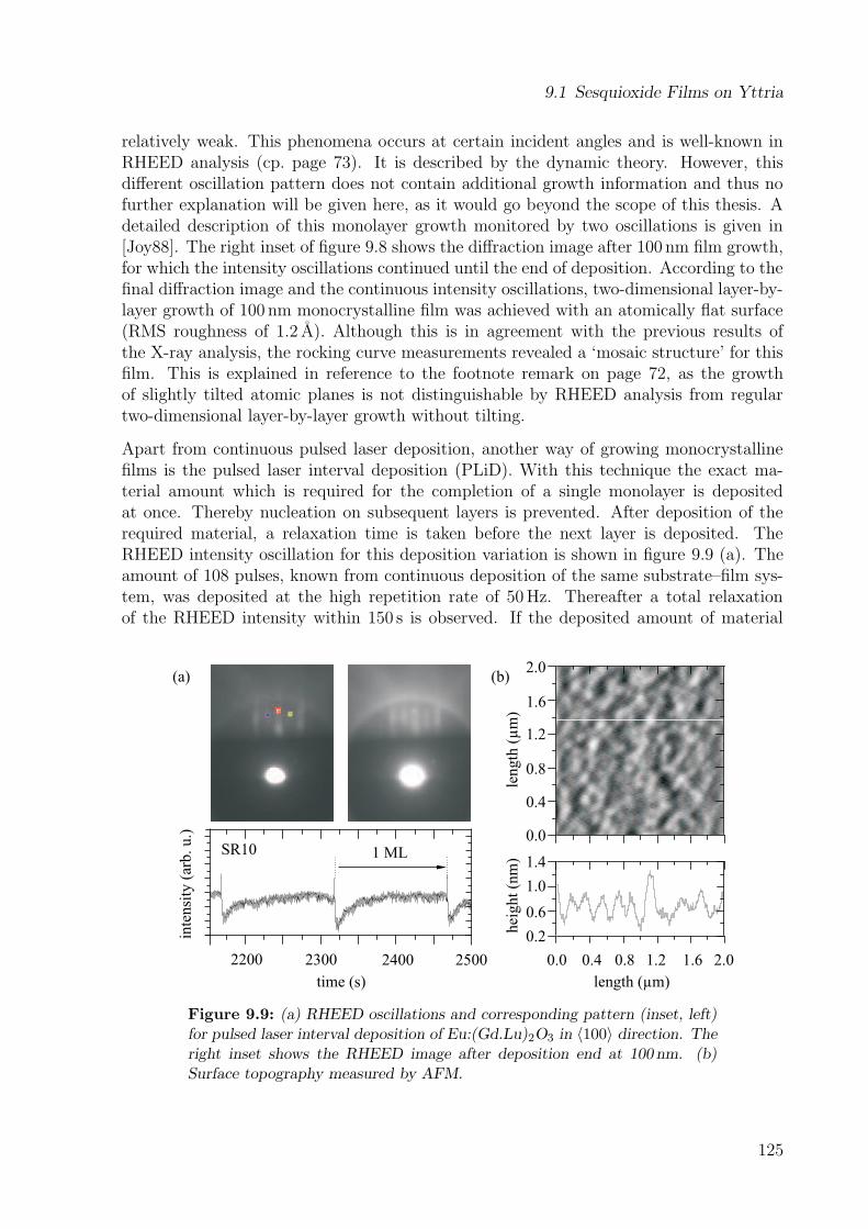
9.1 Sesquioxide Films on Yttria
relatively weak. This phenomena occurs at certain incident angles and is well-known inRHEED analysis (cp. page 73). It is described by the dynamic theory. However, thisdifferent oscillation pattern does not contain additional growth information and thus nofurther explanation will be given here, as it would go beyond the scope of this thesis. Adetailed description of this monolayer growth monitored by two oscillations is given in[Joy88]. The right inset of figure 9.8 shows the diffraction image after 100 nm film growth,for which the intensity oscillations continued until the end of deposition. According to thefinal diffraction image and the continuous intensity oscillations, two-dimensional layer-by-layer growth of 100 nm monocrystalline film was achieved with an atomically flat surface(RMS roughness of 1.2 A). Although this is in agreement with the previous results ofthe X-ray analysis, the rocking curve measurements revealed a ‘mosaic structure’ for thisfilm. This is explained in reference to the footnote remark on page 72, as the growthof slightly tilted atomic planes is not distinguishable by RHEED analysis from regulartwo-dimensional layer-by-layer growth without tilting.
Apart from continuous pulsed laser deposition, another way of growing monocrystallinefilms is the pulsed laser interval deposition (PLiD). With this technique the exact ma-terial amount which is required for the completion of a single monolayer is depositedat once. Thereby nucleation on subsequent layers is prevented. After deposition of therequired material, a relaxation time is taken before the next layer is deposited. TheRHEED intensity oscillation for this deposition variation is shown in figure 9.9 (a). Theamount of 108 pulses, known from continuous deposition of the same substrate–film sys-tem, was deposited at the high repetition rate of 50Hz. Thereafter a total relaxationof the RHEED intensity within 150 s is observed. If the deposited amount of material
inte
nsi
ty (
arb. u.)
2200 2300 2400
time (s)
2500
(a) (b)
length ( m)µ
length
(m
)µ
hei
ght
(nm
)
0.0
0.4
0.8
1.2
1.6
2.0
0.2
0.6
1.0
1.41 ML
0.0 0.4 0.8 1.2 1.6 2.0
SR10
Figure 9.9: (a) RHEED oscillations and corresponding pattern (inset, left)for pulsed laser interval deposition of Eu:(Gd.Lu)2O3 in 〈100〉 direction. Theright inset shows the RHEED image after deposition end at 100 nm. (b)Surface topography measured by AFM.
125
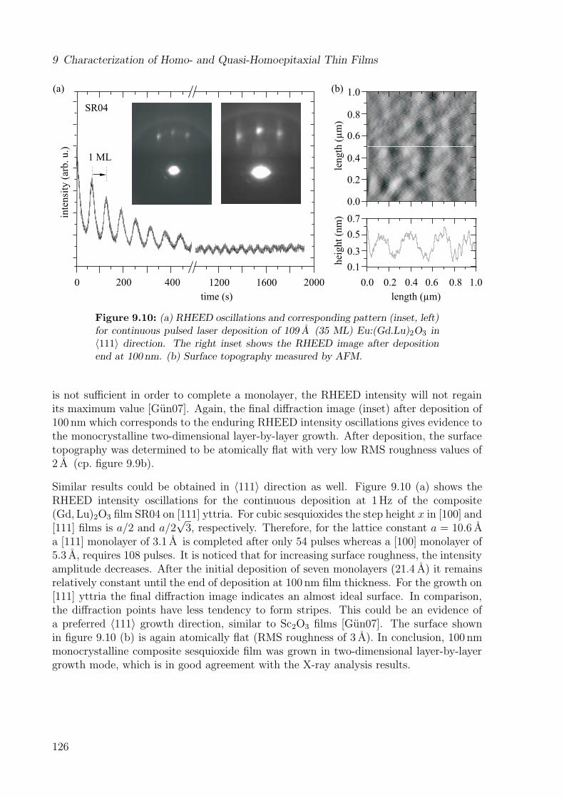
9 Characterization of Homo- and Quasi-Homoepitaxial Thin Filmsin
tensi
ty (
arb. u.)
0 200 400 1200
time (s)
1600 2000
(a) (b)
length ( m)µ
length
(m
)µ
hei
ght
(nm
)
0.0
0.2
0.4
0.6
0.8
1.0
0.1
0.3
0.5
0.7
0.0 0.2 0.4 0.6 0.8 1.0
1 ML
SR04
Figure 9.10: (a) RHEED oscillations and corresponding pattern (inset, left)for continuous pulsed laser deposition of 109 A (35 ML) Eu:(Gd.Lu)2O3 in〈111〉 direction. The right inset shows the RHEED image after depositionend at 100 nm. (b) Surface topography measured by AFM.
is not sufficient in order to complete a monolayer, the RHEED intensity will not regainits maximum value [Gun07]. Again, the final diffraction image (inset) after deposition of100 nm which corresponds to the enduring RHEED intensity oscillations gives evidence tothe monocrystalline two-dimensional layer-by-layer growth. After deposition, the surfacetopography was determined to be atomically flat with very low RMS roughness values of2 A (cp. figure 9.9b).
Similar results could be obtained in 〈111〉 direction as well. Figure 9.10 (a) shows theRHEED intensity oscillations for the continuous deposition at 1Hz of the composite(Gd, Lu)2O3 film SR04 on [111] yttria. For cubic sesquioxides the step height x in [100] and[111] films is a/2 and a/2
√3, respectively. Therefore, for the lattice constant a = 10.6 A
a [111] monolayer of 3.1 A is completed after only 54 pulses whereas a [100] monolayer of5.3 A, requires 108 pulses. It is noticed that for increasing surface roughness, the intensityamplitude decreases. After the initial deposition of seven monolayers (21.4 A) it remainsrelatively constant until the end of deposition at 100 nm film thickness. For the growth on[111] yttria the final diffraction image indicates an almost ideal surface. In comparison,the diffraction points have less tendency to form stripes. This could be an evidence ofa preferred 〈111〉 growth direction, similar to Sc2O3 films [Gun07]. The surface shownin figure 9.10 (b) is again atomically flat (RMS roughness of 3 A). In conclusion, 100 nmmonocrystalline composite sesquioxide film was grown in two-dimensional layer-by-layergrowth mode, which is in good agreement with the X-ray analysis results.
126
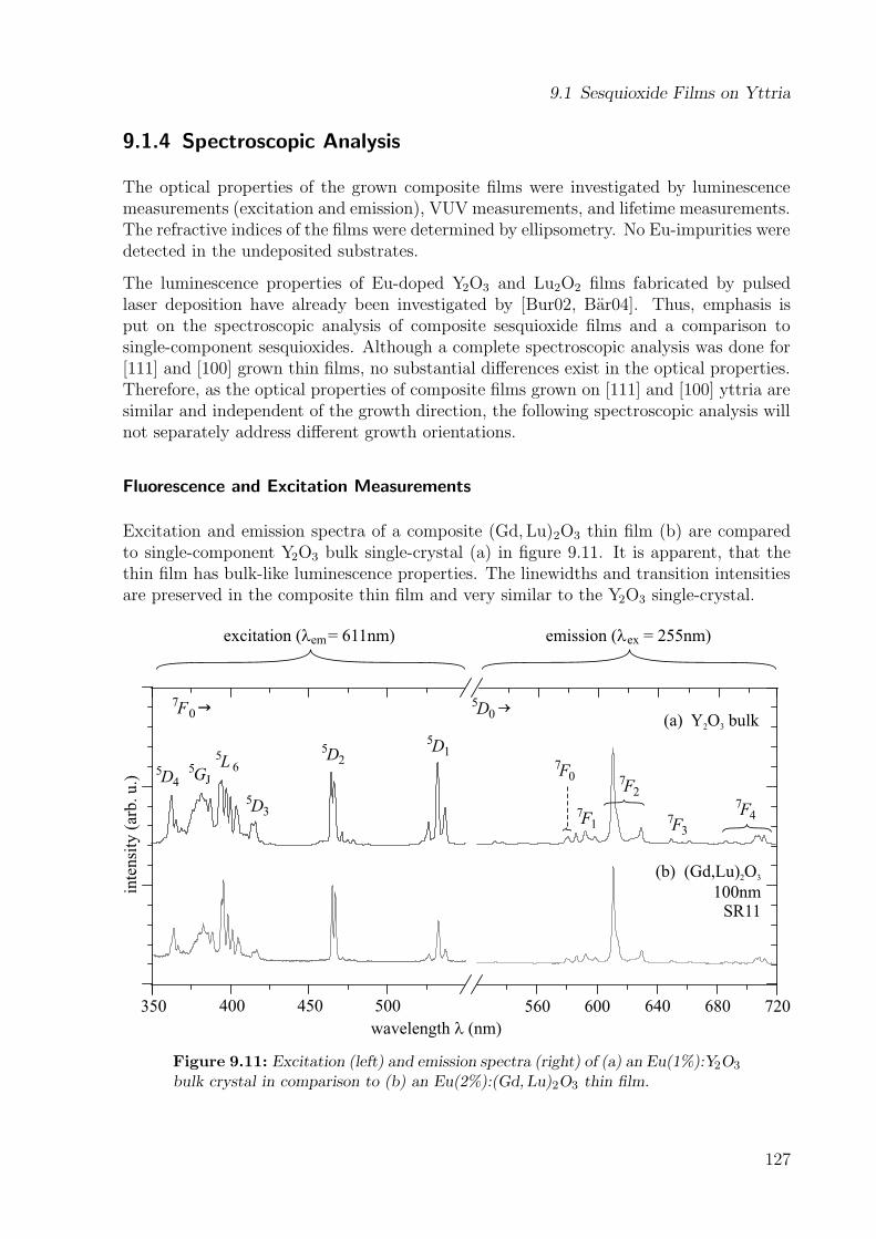
9.1 Sesquioxide Films on Yttria
9.1.4 Spectroscopic Analysis
The optical properties of the grown composite films were investigated by luminescencemeasurements (excitation and emission), VUV measurements, and lifetime measurements.The refractive indices of the films were determined by ellipsometry. No Eu-impurities weredetected in the undeposited substrates.
The luminescence properties of Eu-doped Y2O3 and Lu2O2 films fabricated by pulsedlaser deposition have already been investigated by [Bur02, Bar04]. Thus, emphasis isput on the spectroscopic analysis of composite sesquioxide films and a comparison tosingle-component sesquioxides. Although a complete spectroscopic analysis was done for[111] and [100] grown thin films, no substantial differences exist in the optical properties.Therefore, as the optical properties of composite films grown on [111] and [100] yttria aresimilar and independent of the growth direction, the following spectroscopic analysis willnot separately address different growth orientations.
Fluorescence and Excitation Measurements
Excitation and emission spectra of a composite (Gd, Lu)2O3 thin film (b) are comparedto single-component Y2O3 bulk single-crystal (a) in figure 9.11. It is apparent, that thethin film has bulk-like luminescence properties. The linewidths and transition intensitiesare preserved in the composite thin film and very similar to the Y2O3 single-crystal.
wavelength (nm)l
350 400 450 600 640 680 720
(a) Y O bulk2 3
(b) (Gd,Lu) O
100nmSR11
2 3
inte
nsi
ty (
arb
. u
.)
excitation ( = 611nm)lem emission ( = 255nm)lex
560
5D1
7F0
5D2
5D3
5L 65
GJ5D4
500
7F2
®5D0
7F3
7F4
®7F0
7F1
Figure 9.11: Excitation (left) and emission spectra (right) of (a) an Eu(1%):Y2O3
bulk crystal in comparison to (b) an Eu(2%):(Gd, Lu)2O3 thin film.
127
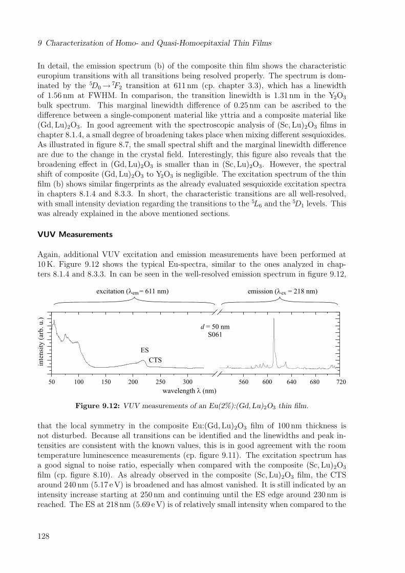
9 Characterization of Homo- and Quasi-Homoepitaxial Thin Films
In detail, the emission spectrum (b) of the composite thin film shows the characteristiceuropium transitions with all transitions being resolved properly. The spectrum is dom-inated by the 5D0→ 7F2 transition at 611 nm (cp. chapter 3.3), which has a linewidthof 1.56 nm at FWHM. In comparison, the transition linewidth is 1.31 nm in the Y2O3
bulk spectrum. This marginal linewidth difference of 0.25 nm can be ascribed to thedifference between a single-component material like yttria and a composite material like(Gd, Lu)2O3. In good agreement with the spectroscopic analysis of (Sc, Lu)2O3 films inchapter 8.1.4, a small degree of broadening takes place when mixing different sesquioxides.As illustrated in figure 8.7, the small spectral shift and the marginal linewidth differenceare due to the change in the crystal field. Interestingly, this figure also reveals that thebroadening effect in (Gd, Lu)2O3 is smaller than in (Sc, Lu)2O3. However, the spectralshift of composite (Gd, Lu)2O3 to Y2O3 is negligible. The excitation spectrum of the thinfilm (b) shows similar fingerprints as the already evaluated sesquioxide excitation spectrain chapters 8.1.4 and 8.3.3. In short, the characteristic transitions are all well-resolved,with small intensity deviation regarding the transitions to the 5L6 and the 5D1 levels. Thiswas already explained in the above mentioned sections.
VUV Measurements
Again, additional VUV excitation and emission measurements have been performed at10K. Figure 9.12 shows the typical Eu-spectra, similar to the ones analyzed in chap-ters 8.1.4 and 8.3.3. In can be seen in the well-resolved emission spectrum in figure 9.12,
50 100 150 200 250 300 560 600 640 720
wavelength (nm)l
inte
nsi
ty (
arb
. u
.)
excitation ( = 611 nm)lem emission ( = 218 nm)lex
ES
CTS
680
d = 50 nmS061
Figure 9.12: VUV measurements of an Eu(2%):(Gd, Lu)2O3 thin film.
that the local symmetry in the composite Eu:(Gd, Lu)2O3 film of 100 nm thickness isnot disturbed. Because all transitions can be identified and the linewidths and peak in-tensities are consistent with the known values, this is in good agreement with the roomtemperature luminescence measurements (cp. figure 9.11). The excitation spectrum hasa good signal to noise ratio, especially when compared with the composite (Sc, Lu)2O3
film (cp. figure 8.10). As already observed in the composite (Sc, Lu)2O3 film, the CTSaround 240 nm (5.17 eV) is broadened and has almost vanished. It is still indicated by anintensity increase starting at 250 nm and continuing until the ES edge around 230 nm isreached. The ES at 218 nm (5.69 eV) is of relatively small intensity when compared to the
128
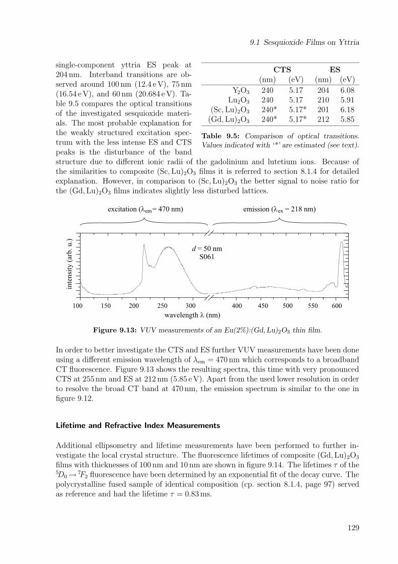
9.1 Sesquioxide Films on Yttria
CTS ES(nm) (eV) (nm) (eV)
Y2O3 240 5.17 204 6.08Lu2O3 240 5.17 210 5.91
(Sc,Lu)2O3 240* 5.17* 201 6.18(Gd,Lu)2O3 240* 5.17* 212 5.85
Table 9.5: Comparison of optical transitions.Values indicated with ‘*’ are estimated (see text).
single-component yttria ES peak at204 nm. Interband transitions are ob-served around 100 nm (12.4 eV), 75 nm(16.54 eV), and 60 nm (20.684 eV). Ta-ble 9.5 compares the optical transitionsof the investigated sesquioxide materi-als. The most probable explanation forthe weakly structured excitation spec-trum with the less intense ES and CTSpeaks is the disturbance of the bandstructure due to different ionic radii of the gadolinium and lutetium ions. Because ofthe similarities to composite (Sc, Lu)2O3 films it is referred to section 8.1.4 for detailedexplanation. However, in comparison to (Sc, Lu)2O3 the better signal to noise ratio forthe (Gd, Lu)2O3 films indicates slightly less disturbed lattices.
100 150 200 250 300 450 500 550400
wavelength (nm)l
inte
nsi
ty (
arb. u.)
excitation ( = 470 nm)lem emission ( = 218 nm)lex
600
d = 50 nmS061
Figure 9.13: VUV measurements of an Eu(2%):(Gd, Lu)2O3 thin film.
In order to better investigate the CTS and ES further VUV measurements have been doneusing a different emission wavelength of λem = 470 nm which corresponds to a broadbandCT fluorescence. Figure 9.13 shows the resulting spectra, this time with very pronouncedCTS at 255 nm and ES at 212 nm (5.85 eV). Apart from the used lower resolution in orderto resolve the broad CT band at 470 nm, the emission spectrum is similar to the one infigure 9.12.
Lifetime and Refractive Index Measurements
Additional ellipsometry and lifetime measurements have been performed to further in-vestigate the local crystal structure. The fluorescence lifetimes of composite (Gd, Lu)2O3
films with thicknesses of 100 nm and 10 nm are shown in figure 9.14. The lifetimes τ of the5D0→ 7F2 fluorescence have been determined by an exponential fit of the decay curve. Thepolycrystalline fused sample of identical composition (cp. section 8.1.4, page 97) servedas reference and had the lifetime τ = 0.83ms.
129
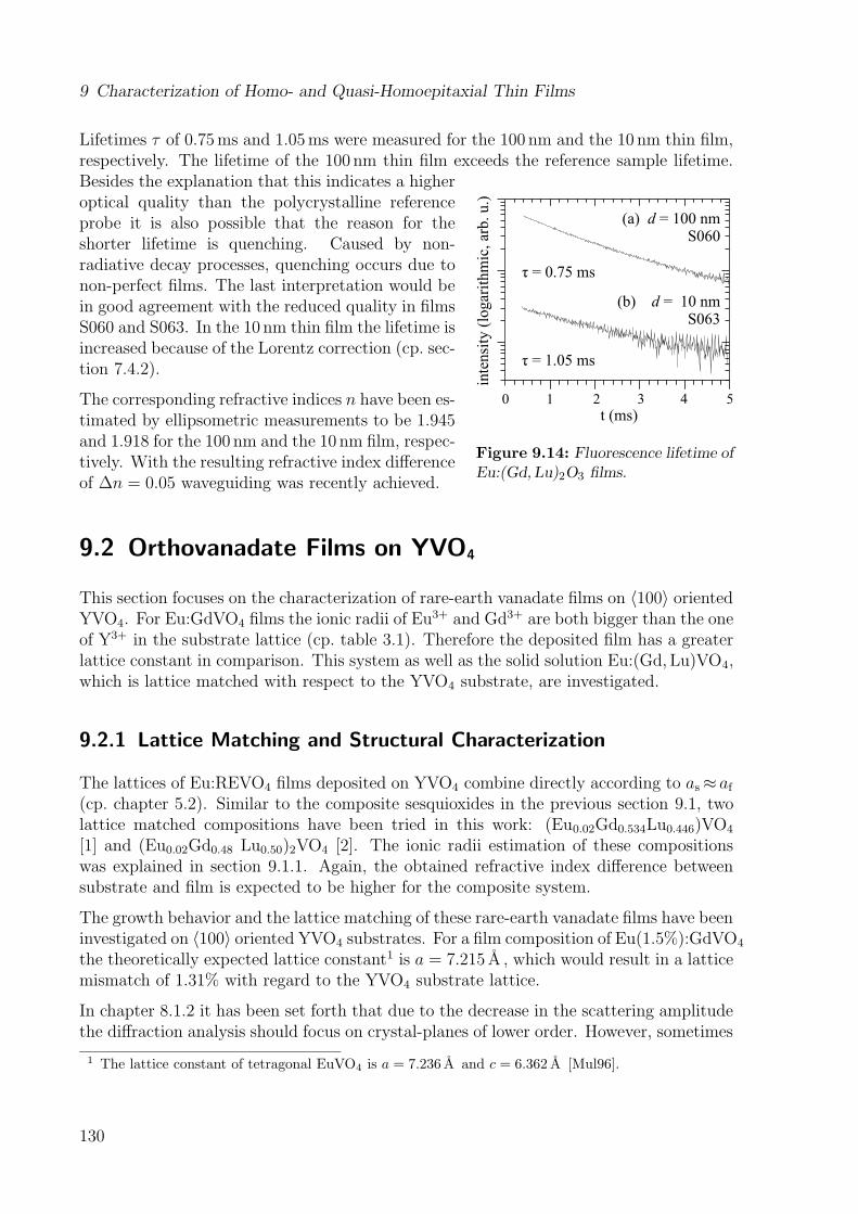
9 Characterization of Homo- and Quasi-Homoepitaxial Thin Films
Lifetimes τ of 0.75ms and 1.05ms were measured for the 100 nm and the 10 nm thin film,respectively. The lifetime of the 100 nm thin film exceeds the reference sample lifetime.
0 1 4 52 3
t (ms)
inte
nsi
ty (
logar
ithm
ic, ar
b. u.)
ô = 0.75 ms
(a) = 100 nmS060
d
(b) = 10 nmS063
d
ô = 1.05 ms
Figure 9.14: Fluorescence lifetime ofEu:(Gd, Lu)2O3 films.
Besides the explanation that this indicates a higheroptical quality than the polycrystalline referenceprobe it is also possible that the reason for theshorter lifetime is quenching. Caused by non-radiative decay processes, quenching occurs due tonon-perfect films. The last interpretation would bein good agreement with the reduced quality in filmsS060 and S063. In the 10 nm thin film the lifetime isincreased because of the Lorentz correction (cp. sec-tion 7.4.2).
The corresponding refractive indices n have been es-timated by ellipsometric measurements to be 1.945and 1.918 for the 100 nm and the 10 nm film, respec-tively. With the resulting refractive index differenceof ∆n = 0.05 waveguiding was recently achieved.
9.2 Orthovanadate Films on YVO4
This section focuses on the characterization of rare-earth vanadate films on 〈100〉 orientedYVO4. For Eu:GdVO4 films the ionic radii of Eu3+ and Gd3+ are both bigger than the oneof Y3+ in the substrate lattice (cp. table 3.1). Therefore the deposited film has a greaterlattice constant in comparison. This system as well as the solid solution Eu:(Gd, Lu)VO4,which is lattice matched with respect to the YVO4 substrate, are investigated.
9.2.1 Lattice Matching and Structural Characterization
The lattices of Eu:REVO4 films deposited on YVO4 combine directly according to as≈ af(cp. chapter 5.2). Similar to the composite sesquioxides in the previous section 9.1, twolattice matched compositions have been tried in this work: (Eu0.02Gd0.534Lu0.446)VO4
[1] and (Eu0.02Gd0.48 Lu0.50)2VO4 [2]. The ionic radii estimation of these compositionswas explained in section 9.1.1. Again, the obtained refractive index difference betweensubstrate and film is expected to be higher for the composite system.
The growth behavior and the lattice matching of these rare-earth vanadate films have beeninvestigated on 〈100〉 oriented YVO4 substrates. For a film composition of Eu(1.5%):GdVO4
the theoretically expected lattice constant1 is a = 7.215 A , which would result in a latticemismatch of 1.31% with regard to the YVO4 substrate lattice.
In chapter 8.1.2 it has been set forth that due to the decrease in the scattering amplitudethe diffraction analysis should focus on crystal-planes of lower order. However, sometimes
1 The lattice constant of tetragonal EuVO4 is a = 7.236 A and c = 6.362 A [Mul96].
130

9.2 Orthovanadate Films on YVO4
a strong overlap of substrate and film reflections prevents a differentiated diffractionanalysis. This is especially the case in homo- and quasi-homoepitaxial films. Therefore,as the diffraction spectra are widened with increasing 2θ angle, crystal-planes of higherorder are analyzed in these exceptions. The f values in tables 9.6 and 9.7 indicated with‘*’ are calculated by deriving film and substrate lattice constants from the diffractionspectra, as the diffraction measurements may vary ± 0.05 � in absolute positions. Thus,the values of a⊥ do not reflect the real mismatch parameter f .
Gadolinium Vanadate Films
In figure 9.15 two diffraction spectra of Eu-doped GdVO4 films are compared and theacquired film properties summarized in table 9.6. Despite having the same film composi-tion, different degrees of lattice matching are achieved with mismatch values f of 1.72%and 0.92% for films S020 and S080. This is understood with regard to the depositionparameters. Although both films were deposited under the same oxygen atmosphere of10−2mbar, the repetition rate was varied from 11Hz (S020) to 3Hz (S080).
Especially the higher deposition temperature of 850 � C for film S080 has strong influence
inte
nsi
ty (
logar
ithm
ic, ar
b. unit
s)
*
(a) S020
(b) S080
{400}
*
inte
nsi
ty (
arb. u.)
24 25 26
film
25 30 35 40 45 5520 50
2 (degree)q
inte
nsi
ty (
arb. u.)
24.0 24.824.4
film
{200}
{400}{200}
Figure 9.15: X-ray diffraction patterns of Eu(1.5%):GdVO4 films grown on 〈100〉oriented YVO4: (a) 125 nm thin film and (b) 100 nm thin film. The insets showadditional high resolution scans. Diffraction peaks indicated with ‘*’ result from theresidual Cu-Kβ emission.
131
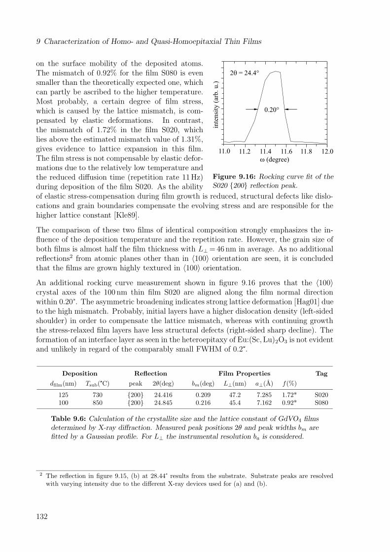
9 Characterization of Homo- and Quasi-Homoepitaxial Thin Films
inte
nsi
ty (
arb
. u
.)
11.0 11.2 11.4 11.6 11.8 12.0
w (degree)
0.20°
2 = 24.4°q
Figure 9.16: Rocking curve fit of theS020 {200} reflection peak.
on the surface mobility of the deposited atoms.The mismatch of 0.92% for the film S080 is evensmaller than the theoretically expected one, whichcan partly be ascribed to the higher temperature.Most probably, a certain degree of film stress,which is caused by the lattice mismatch, is com-pensated by elastic deformations. In contrast,the mismatch of 1.72% in the film S020, whichlies above the estimated mismatch value of 1.31%,gives evidence to lattice expansion in this film.The film stress is not compensable by elastic defor-mations due to the relatively low temperature andthe reduced diffusion time (repetition rate 11Hz)during deposition of the film S020. As the abilityof elastic stress-compensation during film growth is reduced, structural defects like dislo-cations and grain boundaries compensate the evolving stress and are responsible for thehigher lattice constant [Kle89].
The comparison of these two films of identical composition strongly emphasizes the in-fluence of the deposition temperature and the repetition rate. However, the grain size ofboth films is almost half the film thickness with L⊥=46nm in average. As no additionalreflections2 from atomic planes other than in 〈100〉 orientation are seen, it is concludedthat the films are grown highly textured in 〈100〉 orientation.
An additional rocking curve measurement shown in figure 9.16 proves that the 〈100〉crystal axes of the 100 nm thin film S020 are aligned along the film normal directionwithin 0.20 � . The asymmetric broadening indicates strong lattice deformation [Hag01] dueto the high mismatch. Probably, initial layers have a higher dislocation density (left-sidedshoulder) in order to compensate the lattice mismatch, whereas with continuing growththe stress-relaxed film layers have less structural defects (right-sided sharp decline). Theformation of an interface layer as seen in the heteroepitaxy of Eu:(Sc, Lu)2O3 is not evidentand unlikely in regard of the comparably small FWHM of 0.2 � .
Deposition Reflection Film Properties Tag
dfilm(nm) Tsub( � C) peak 2θ(deg) bm(deg) L⊥(nm) a⊥(A) f(%)
125 730 {200} 24.416 0.209 47.2 7.285 1.72* S020100 850 {200} 24.845 0.216 45.4 7.162 0.92* S080
Table 9.6: Calculation of the crystallite size and the lattice constant of GdVO4 filmsdetermined by X-ray diffraction. Measured peak positions 2θ and peak widths bm arefitted by a Gaussian profile. For L⊥ the instrumental resolution ba is considered.
2 The reflection in figure 9.15, (b) at 28.44 � results from the substrate. Substrate peaks are resolvedwith varying intensity due to the different X-ray devices used for (a) and (b).
132
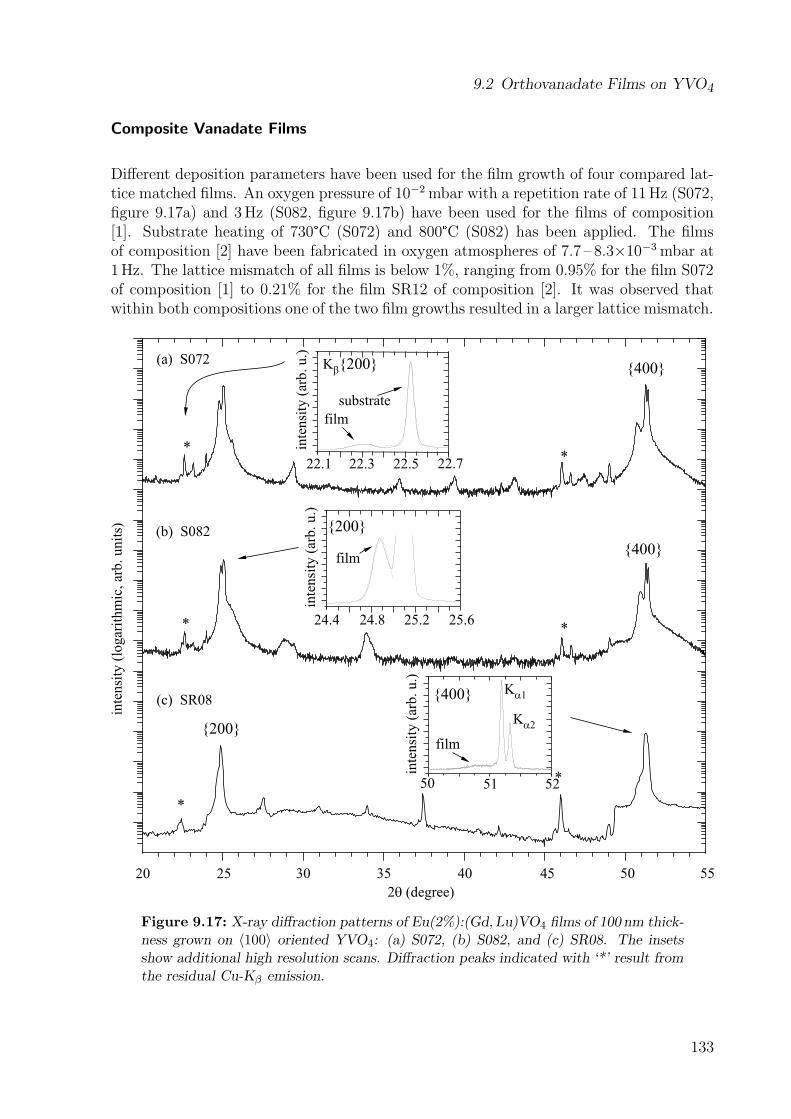
9.2 Orthovanadate Films on YVO4
Composite Vanadate Films
Different deposition parameters have been used for the film growth of four compared lat-tice matched films. An oxygen pressure of 10−2mbar with a repetition rate of 11Hz (S072,figure 9.17a) and 3Hz (S082, figure 9.17b) have been used for the films of composition[1]. Substrate heating of 730 � C (S072) and 800 � C (S082) has been applied. The filmsof composition [2] have been fabricated in oxygen atmospheres of 7.7 – 8.3×10⁻³mbar at1Hz. The lattice mismatch of all films is below 1%, ranging from 0.95% for the film S072of composition [1] to 0.21% for the film SR12 of composition [2]. It was observed thatwithin both compositions one of the two film growths resulted in a larger lattice mismatch.
inte
nsi
ty (
logar
ithm
ic, ar
b. unit
s)
(a) S072
(b) S082
(c) SR08
*
{400}
{200}
{400}
inte
nsi
ty (
arb. u.)
24.4 24.8 25.2 25.6
film
{200}
{400}
{200}
*
25 30 35 40 45 5520 50
2 (degree)q
*
*
film
substrate
Kb
inte
nsi
ty (
arb. u.)
22.1 22.5 22.722.3
inte
nsi
ty (
arb. u.)
50 5251
film
Ka2
Ka1
* *
Figure 9.17: X-ray diffraction patterns of Eu(2%):(Gd, Lu)VO4 films of 100 nm thick-ness grown on 〈100〉 oriented YVO4: (a) S072, (b) S082, and (c) SR08. The insetsshow additional high resolution scans. Diffraction peaks indicated with ‘*’ result fromthe residual Cu-Kβ emission.
133
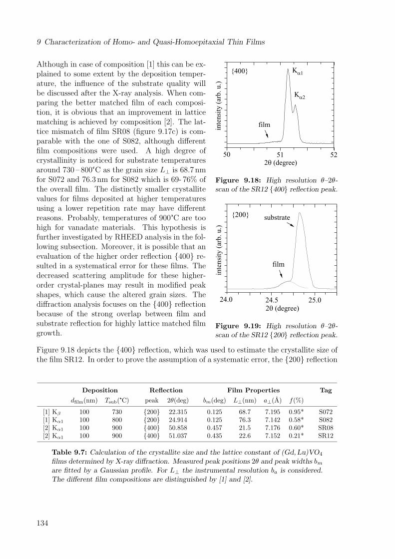
9 Characterization of Homo- and Quasi-Homoepitaxial Thin Films
50 5251
inte
nsi
ty (
arb
. u
.)
2q (degree)
{400}
film
Ka2
Ka1
Figure 9.18: High resolution θ–2θ-scan of the SR12 {400} reflection peak.
inte
nsi
ty (
arb
. u
.)
24.0 24.5 25.02q (degree)
{200}
film
substrate
Figure 9.19: High resolution θ–2θ-scan of the SR12 {200} reflection peak.
Although in case of composition [1] this can be ex-plained to some extent by the deposition temper-ature, the influence of the substrate quality willbe discussed after the X-ray analysis. When com-paring the better matched film of each composi-tion, it is obvious that an improvement in latticematching is achieved by composition [2]. The lat-tice mismatch of film SR08 (figure 9.17c) is com-parable with the one of S082, although differentfilm compositions were used. A high degree ofcrystallinity is noticed for substrate temperaturesaround 730 – 800 � C as the grain size L⊥ is 68.7 nmfor S072 and 76.3 nm for S082 which is 69- 76% ofthe overall film. The distinctly smaller crystallitevalues for films deposited at higher temperaturesusing a lower repetition rate may have differentreasons. Probably, temperatures of 900 � C are toohigh for vanadate materials. This hypothesis isfurther investigated by RHEED analysis in the fol-lowing subsection. Moreover, it is possible that anevaluation of the higher order reflection {400} re-sulted in a systematical error for these films. Thedecreased scattering amplitude for these higher-order crystal-planes may result in modified peakshapes, which cause the altered grain sizes. Thediffraction analysis focuses on the {400} reflectionbecause of the strong overlap between film andsubstrate reflection for highly lattice matched filmgrowth.
Figure 9.18 depicts the {400} reflection, which was used to estimate the crystallite size ofthe film SR12. In order to prove the assumption of a systematic error, the {200} reflection
Deposition Reflection Film Properties Tag
dfilm(nm) Tsub( � C) peak 2θ(deg) bm(deg) L⊥(nm) a⊥(A) f(%)
[1] Kβ 100 730 {200} 22.315 0.125 68.7 7.195 0.95* S072[1] Kα1 100 800 {200} 24.914 0.125 76.3 7.142 0.58* S082[2] Kα1 100 900 {400} 50.858 0.457 21.5 7.176 0.60* SR08[2] Kα1 100 900 {400} 51.037 0.435 22.6 7.152 0.21* SR12
Table 9.7: Calculation of the crystallite size and the lattice constant of (Gd, Lu)VO4
films determined by X-ray diffraction. Measured peak positions 2θ and peak widths bmare fitted by a Gaussian profile. For L⊥ the instrumental resolution ba is considered.The different film compositions are distinguished by [1] and [2].
134
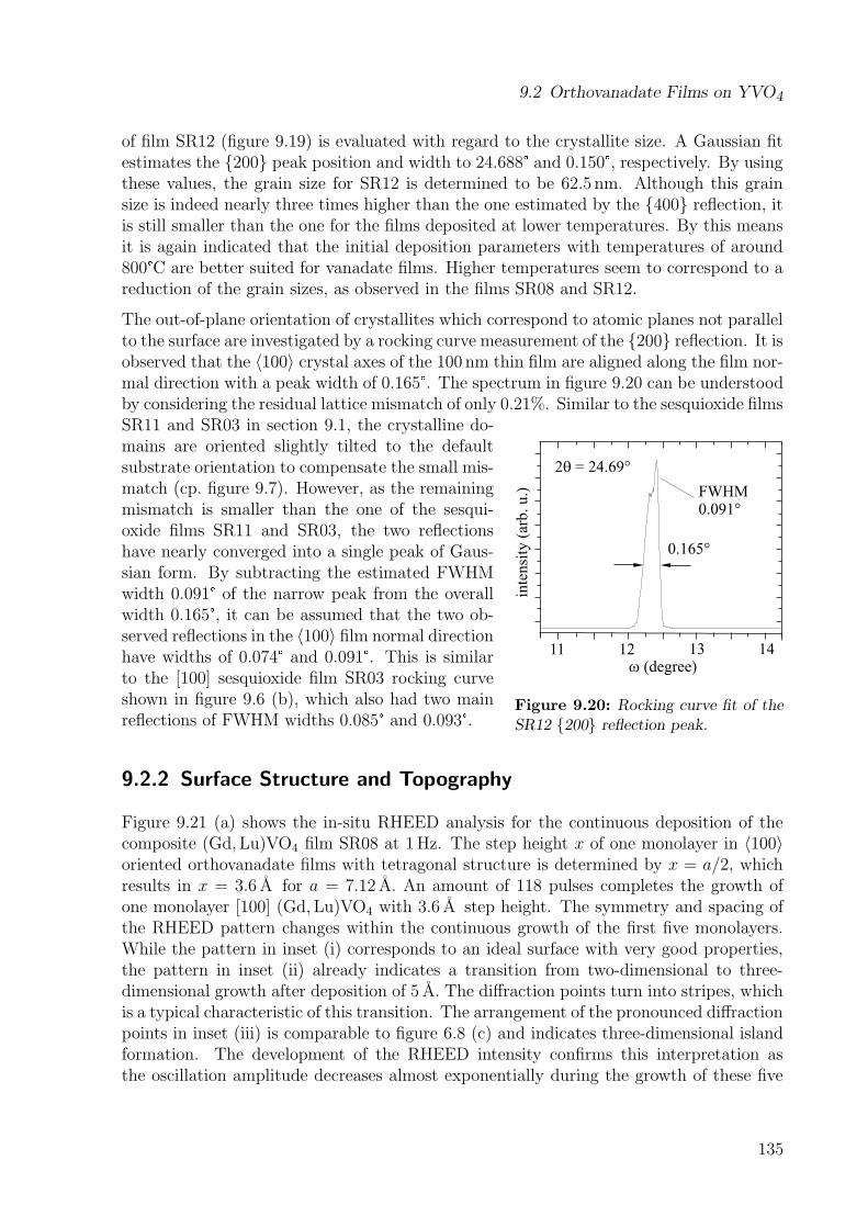
9.2 Orthovanadate Films on YVO4
of film SR12 (figure 9.19) is evaluated with regard to the crystallite size. A Gaussian fitestimates the {200} peak position and width to 24.688 � and 0.150 � , respectively. By usingthese values, the grain size for SR12 is determined to be 62.5 nm. Although this grainsize is indeed nearly three times higher than the one estimated by the {400} reflection, itis still smaller than the one for the films deposited at lower temperatures. By this meansit is again indicated that the initial deposition parameters with temperatures of around800 � C are better suited for vanadate films. Higher temperatures seem to correspond to areduction of the grain sizes, as observed in the films SR08 and SR12.
The out-of-plane orientation of crystallites which correspond to atomic planes not parallelto the surface are investigated by a rocking curve measurement of the {200} reflection. It isobserved that the 〈100〉 crystal axes of the 100 nm thin film are aligned along the film nor-mal direction with a peak width of 0.165 � . The spectrum in figure 9.20 can be understoodby considering the residual lattice mismatch of only 0.21%. Similar to the sesquioxide films
w (degree)
inte
nsi
ty (
arb
. u
.)
11 12 13 14
2 = 24.69°q
0.165°
FWHM0.091°
Figure 9.20: Rocking curve fit of theSR12 {200} reflection peak.
SR11 and SR03 in section 9.1, the crystalline do-mains are oriented slightly tilted to the defaultsubstrate orientation to compensate the small mis-match (cp. figure 9.7). However, as the remainingmismatch is smaller than the one of the sesqui-oxide films SR11 and SR03, the two reflectionshave nearly converged into a single peak of Gaus-sian form. By subtracting the estimated FWHMwidth 0.091 � of the narrow peak from the overallwidth 0.165 � , it can be assumed that the two ob-served reflections in the 〈100〉 film normal directionhave widths of 0.074 � and 0.091 � . This is similarto the [100] sesquioxide film SR03 rocking curveshown in figure 9.6 (b), which also had two mainreflections of FWHM widths 0.085 � and 0.093 � .
9.2.2 Surface Structure and Topography
Figure 9.21 (a) shows the in-situ RHEED analysis for the continuous deposition of thecomposite (Gd, Lu)VO4 film SR08 at 1Hz. The step height x of one monolayer in 〈100〉oriented orthovanadate films with tetragonal structure is determined by x = a/2, whichresults in x = 3.6 A for a = 7.12 A. An amount of 118 pulses completes the growth ofone monolayer [100] (Gd, Lu)VO4 with 3.6 A step height. The symmetry and spacing ofthe RHEED pattern changes within the continuous growth of the first five monolayers.While the pattern in inset (i) corresponds to an ideal surface with very good properties,the pattern in inset (ii) already indicates a transition from two-dimensional to three-dimensional growth after deposition of 5 A. The diffraction points turn into stripes, whichis a typical characteristic of this transition. The arrangement of the pronounced diffractionpoints in inset (iii) is comparable to figure 6.8 (c) and indicates three-dimensional islandformation. The development of the RHEED intensity confirms this interpretation asthe oscillation amplitude decreases almost exponentially during the growth of these five
135
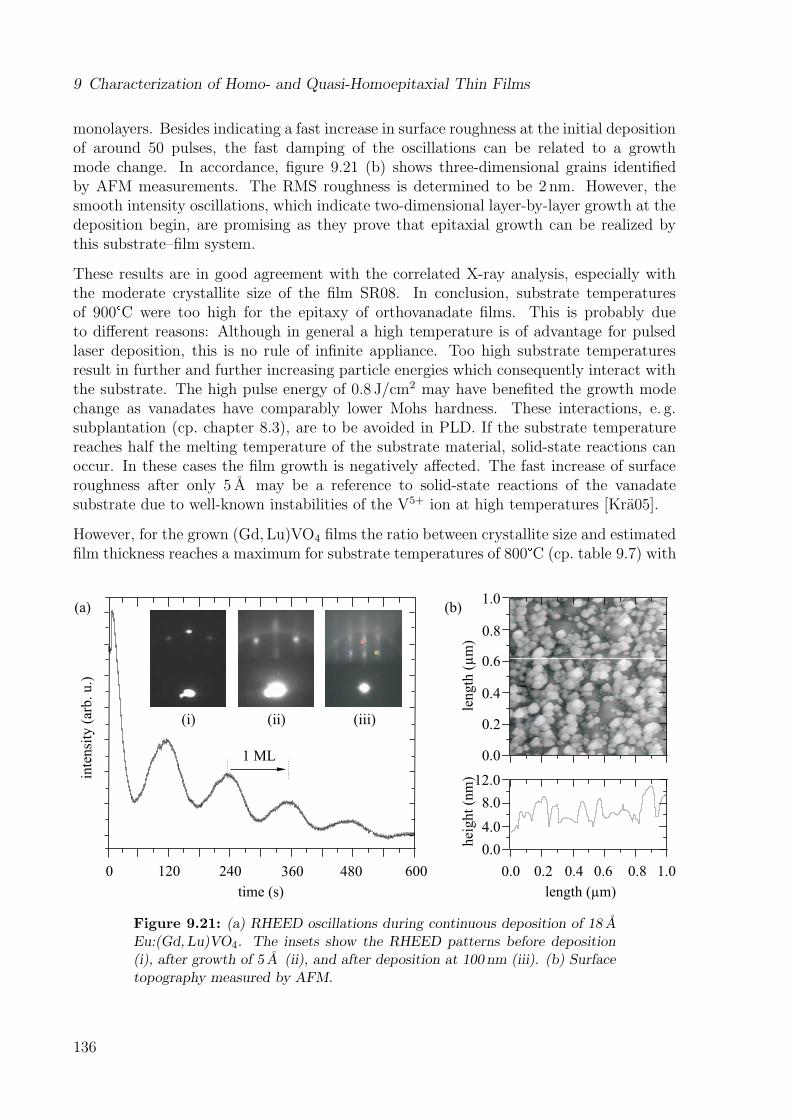
9 Characterization of Homo- and Quasi-Homoepitaxial Thin Films
monolayers. Besides indicating a fast increase in surface roughness at the initial depositionof around 50 pulses, the fast damping of the oscillations can be related to a growthmode change. In accordance, figure 9.21 (b) shows three-dimensional grains identifiedby AFM measurements. The RMS roughness is determined to be 2 nm. However, thesmooth intensity oscillations, which indicate two-dimensional layer-by-layer growth at thedeposition begin, are promising as they prove that epitaxial growth can be realized bythis substrate–film system.
These results are in good agreement with the correlated X-ray analysis, especially withthe moderate crystallite size of the film SR08. In conclusion, substrate temperaturesof 900 � C were too high for the epitaxy of orthovanadate films. This is probably dueto different reasons: Although in general a high temperature is of advantage for pulsedlaser deposition, this is no rule of infinite appliance. Too high substrate temperaturesresult in further and further increasing particle energies which consequently interact withthe substrate. The high pulse energy of 0.8 J/cm2 may have benefited the growth modechange as vanadates have comparably lower Mohs hardness. These interactions, e. g.subplantation (cp. chapter 8.3), are to be avoided in PLD. If the substrate temperaturereaches half the melting temperature of the substrate material, solid-state reactions canoccur. In these cases the film growth is negatively affected. The fast increase of surfaceroughness after only 5 A may be a reference to solid-state reactions of the vanadatesubstrate due to well-known instabilities of the V5+ ion at high temperatures [Kra05].
However, for the grown (Gd, Lu)VO4 films the ratio between crystallite size and estimatedfilm thickness reaches a maximum for substrate temperatures of 800 � C (cp. table 9.7) with
inte
nsi
ty (
arb
. u
.)
0 120 240 360
time (s)
480 600
(a) (b)
0.0 0.2 0.4 0.6 0.8 1.0
length ( m)µ
length
(m
)µ
hei
ght
(nm
)
0.0
0.2
0.4
0.6
0.8
1.0
0.0
4.0
8.0
12.0
1 ML
(i) (ii) (iii)
Figure 9.21: (a) RHEED oscillations during continuous deposition of 18 AEu:(Gd, Lu)VO4. The insets show the RHEED patterns before deposition(i), after growth of 5 A (ii), and after deposition at 100 nm (iii). (b) Surfacetopography measured by AFM.
136
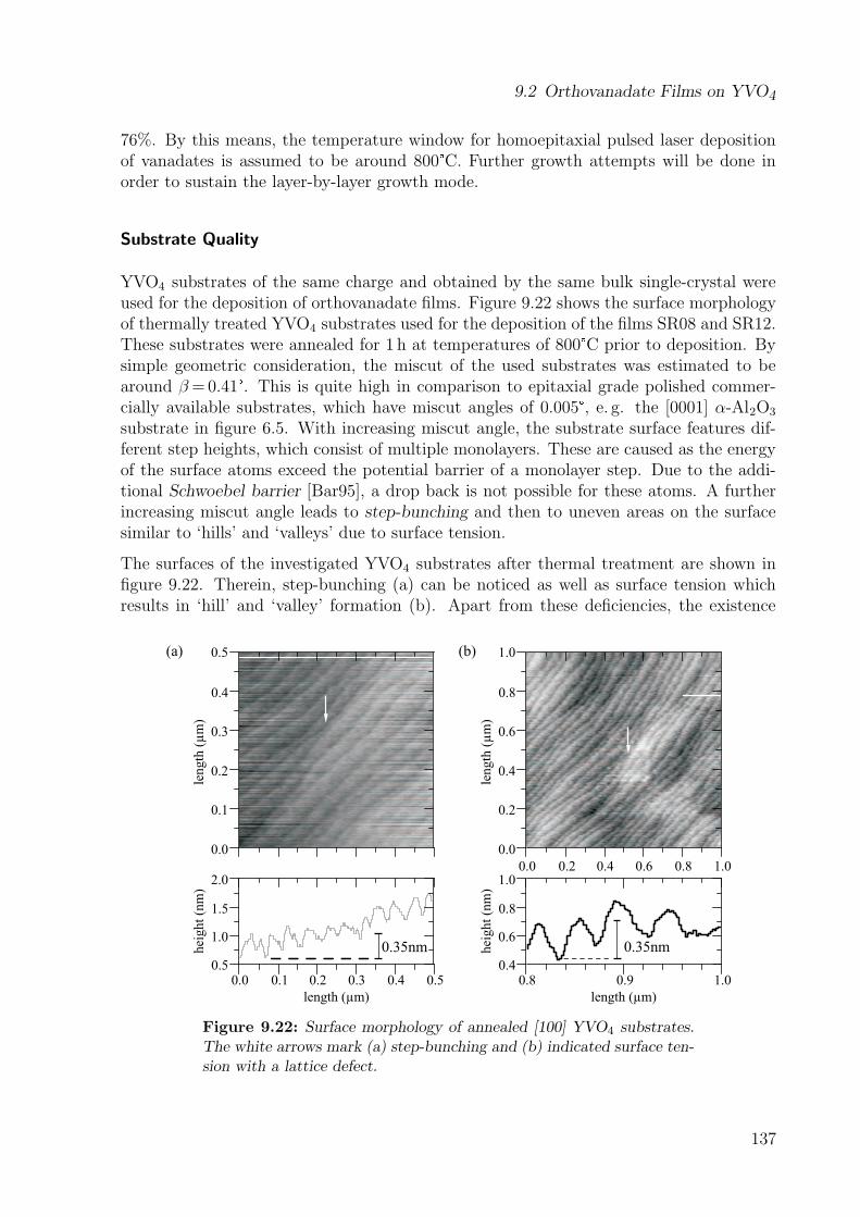
9.2 Orthovanadate Films on YVO4
76%. By this means, the temperature window for homoepitaxial pulsed laser depositionof vanadates is assumed to be around 800 � C. Further growth attempts will be done inorder to sustain the layer-by-layer growth mode.
Substrate Quality
YVO4 substrates of the same charge and obtained by the same bulk single-crystal wereused for the deposition of orthovanadate films. Figure 9.22 shows the surface morphologyof thermally treated YVO4 substrates used for the deposition of the films SR08 and SR12.These substrates were annealed for 1 h at temperatures of 800 � C prior to deposition. Bysimple geometric consideration, the miscut of the used substrates was estimated to bearound β=0.41 � . This is quite high in comparison to epitaxial grade polished commer-cially available substrates, which have miscut angles of 0.005 � , e. g. the [0001] α-Al2O3
substrate in figure 6.5. With increasing miscut angle, the substrate surface features dif-ferent step heights, which consist of multiple monolayers. These are caused as the energyof the surface atoms exceed the potential barrier of a monolayer step. Due to the addi-tional Schwoebel barrier [Bar95], a drop back is not possible for these atoms. A furtherincreasing miscut angle leads to step-bunching and then to uneven areas on the surfacesimilar to ‘hills’ and ‘valleys’ due to surface tension.
The surfaces of the investigated YVO4 substrates after thermal treatment are shown infigure 9.22. Therein, step-bunching (a) can be noticed as well as surface tension whichresults in ‘hill’ and ‘valley’ formation (b). Apart from these deficiencies, the existence
0.8 0.9 1.00.4
0.6
0.8
1.0
0.0
0.2
0.4
0.6
0.8
1.0
length (µm)
hei
ght
(nm
)le
ngth
(µ
m)
0.0 0.2 0.4 0.6 0.8 1.0
0.35nm
0.5
1.0
1.5
2.0
0.0
0.1
0.2
0.3
0.4
0.5
length (µm)
hei
ght
(nm
)le
ngth
(µ
m)
0.0 0.1 0.2 0.3 0.4 0.5
0.35nm
(a) (b)
Figure 9.22: Surface morphology of annealed [100] YVO4 substrates.The white arrows mark (a) step-bunching and (b) indicated surface ten-sion with a lattice defect.
137
9 Characterization of Homo- and Quasi-Homoepitaxial Thin Films
of lattice defects is indicated (b). By this means, the high miscut angles and possiblelattice defects of the substrate may affect the film growth due to the comparably highstep density on the substrate and the indicated surface tension [Joy88, Gun07]. Step-bunching usually causes three-dimensional island growth during the deposition process[Rij04], which would be in agreement with the growth behavior of the film SR08 observedby RHEED.
Therefore, two reasons may probably be responsible for the transition from two-dimensionalto three-dimensional growth: the poor substrate quality (high miscut, step-bunching, lat-tice defects) and the too high substrate temperature during deposition. A correlation ofboth factors is possible.
9.2.3 Spectroscopic Analysis
The optical properties of the grown composite films were investigated by luminescencemeasurements (excitation and emission), VUV measurements, and lifetime measurements.In addition, the refractive indices of the films were determined by ellipsometry. No Eu-impurities were detected in the undeposited substrates.
Fluorescence and Excitation Measurements
Composite orthovanadate films are compared to single-component Eu:GdVO4 as bulkcrystal and as thin film. The charge transfer band for the investigated orthovanadateshas its maximum at around 270 nm. In figure 9.23 it is apparent that the emission spectraare once again dominated by the 5D0→ 7F2 transition at 619 nm with narrow linewidthsof 1.2 nm at FWHM in the GdVO4 bulk crystal (a), of 1.5 nm in the GdVO4 film (b),and of 1.26 nm in the mixed (Gd, Lu)VO4 film (c). For the emission measurements, thelinewidth and transition intensities are preserved in the composite thin films and are verysimilar to the single-component bulk. Equally well-resolved excitation spectra (b) and (c)were measured for the thin films. Only the 5D1 level at around 530 nm is less pronouncedin the thin films than in the bulk crystal. Therefore, the local crystal structure of theEu3+ ions is assumed to be without disturbance.
VUV Measurements
Figure 9.24 shows the VUV excitation and emission spectra which have been carried out atthe SuperLumi station at 10K. Therein, a single-component orthovanadate Eu:GdVO4
thin film (a) is compared with a composite system Eu:(Gd, Lu)VO4 thin film (b). Thefilms are of comparable thickness with 125 nm for GdVO4 and 100 nm for (Gd, Lu)VO4.No bulk crystal was available for comparison purposes.
Basic differences are observed when comparing the excitation measurements. The bandstructure of Eu:GdVO4 (a) reveals the charge transfer state (CTS) peaking at 265 nm(4.68 eV). No excitonic state (ES) is existent in the band structure, however at 204 nm
138
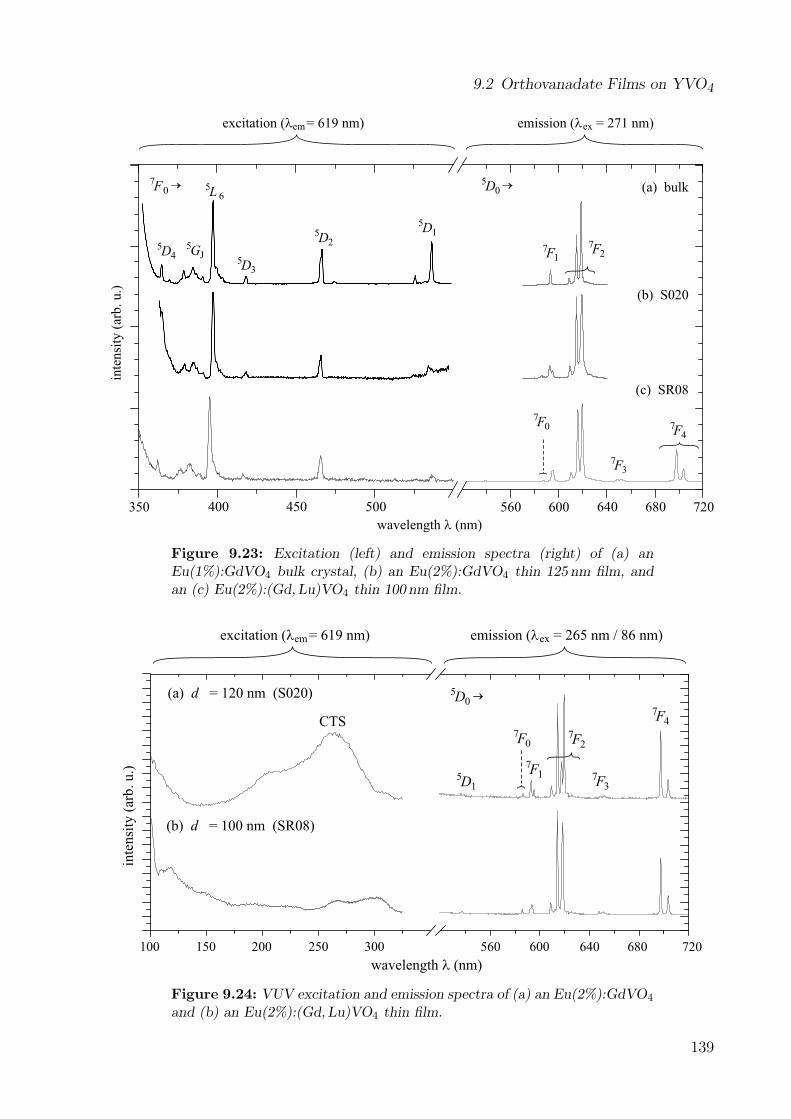
9.2 Orthovanadate Films on YVO4
wavelength (nm)l
350 400 450 600 640 680 720
inte
nsi
ty (
arb
. u
.)excitation ( = 619 nm)lem emission ( = 271 nm)lex
560500
5D15
D2
5D3
5L 6
5GJ
5D4
®7F0
®5D0
7F2
7F1
7F3
7F4
7F0
(a) bulk
(b) S020
(c) SR08
Figure 9.23: Excitation (left) and emission spectra (right) of (a) anEu(1%):GdVO4 bulk crystal, (b) an Eu(2%):GdVO4 thin 125 nm film, andan (c) Eu(2%):(Gd, Lu)VO4 thin 100 nm film.
CTS7F0
7F2
7F3
7F4
7F15
D1
100 150 200 250 300 560 600 640 720
wavelength (nm)l
inte
nsi
ty (
arb. u.)
excitation ( = 619 nm)lem emission ( = 265 nm / 86 nm)lex
680
(a) = 120 nm (S020)d
(b) = 100 nm (SR08)d
®5D0
Figure 9.24: VUV excitation and emission spectra of (a) an Eu(2%):GdVO4
and (b) an Eu(2%):(Gd, Lu)VO4 thin film.
139
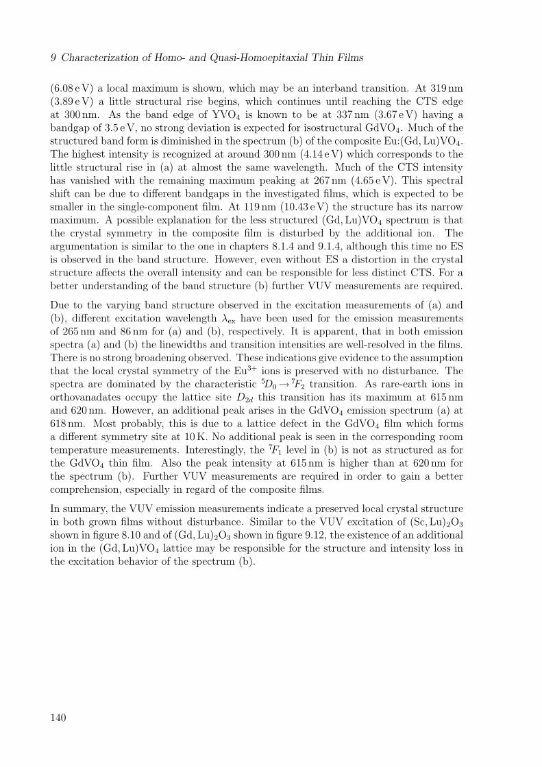
9 Characterization of Homo- and Quasi-Homoepitaxial Thin Films
(6.08 eV) a local maximum is shown, which may be an interband transition. At 319 nm(3.89 eV) a little structural rise begins, which continues until reaching the CTS edgeat 300 nm. As the band edge of YVO4 is known to be at 337 nm (3.67 eV) having abandgap of 3.5 eV, no strong deviation is expected for isostructural GdVO4. Much of thestructured band form is diminished in the spectrum (b) of the composite Eu:(Gd, Lu)VO4.The highest intensity is recognized at around 300 nm (4.14 eV) which corresponds to thelittle structural rise in (a) at almost the same wavelength. Much of the CTS intensityhas vanished with the remaining maximum peaking at 267 nm (4.65 eV). This spectralshift can be due to different bandgaps in the investigated films, which is expected to besmaller in the single-component film. At 119 nm (10.43 eV) the structure has its narrowmaximum. A possible explanation for the less structured (Gd, Lu)VO4 spectrum is thatthe crystal symmetry in the composite film is disturbed by the additional ion. Theargumentation is similar to the one in chapters 8.1.4 and 9.1.4, although this time no ESis observed in the band structure. However, even without ES a distortion in the crystalstructure affects the overall intensity and can be responsible for less distinct CTS. For abetter understanding of the band structure (b) further VUV measurements are required.
Due to the varying band structure observed in the excitation measurements of (a) and(b), different excitation wavelength λex have been used for the emission measurementsof 265 nm and 86 nm for (a) and (b), respectively. It is apparent, that in both emissionspectra (a) and (b) the linewidths and transition intensities are well-resolved in the films.There is no strong broadening observed. These indications give evidence to the assumptionthat the local crystal symmetry of the Eu3+ ions is preserved with no disturbance. Thespectra are dominated by the characteristic 5D0→ 7F2 transition. As rare-earth ions inorthovanadates occupy the lattice site D2d this transition has its maximum at 615 nmand 620 nm. However, an additional peak arises in the GdVO4 emission spectrum (a) at618 nm. Most probably, this is due to a lattice defect in the GdVO4 film which formsa different symmetry site at 10K. No additional peak is seen in the corresponding roomtemperature measurements. Interestingly, the 7F1 level in (b) is not as structured as forthe GdVO4 thin film. Also the peak intensity at 615 nm is higher than at 620 nm forthe spectrum (b). Further VUV measurements are required in order to gain a bettercomprehension, especially in regard of the composite films.
In summary, the VUV emission measurements indicate a preserved local crystal structurein both grown films without disturbance. Similar to the VUV excitation of (Sc, Lu)2O3
shown in figure 8.10 and of (Gd, Lu)2O3 shown in figure 9.12, the existence of an additionalion in the (Gd, Lu)VO4 lattice may be responsible for the structure and intensity loss inthe excitation behavior of the spectrum (b).
140
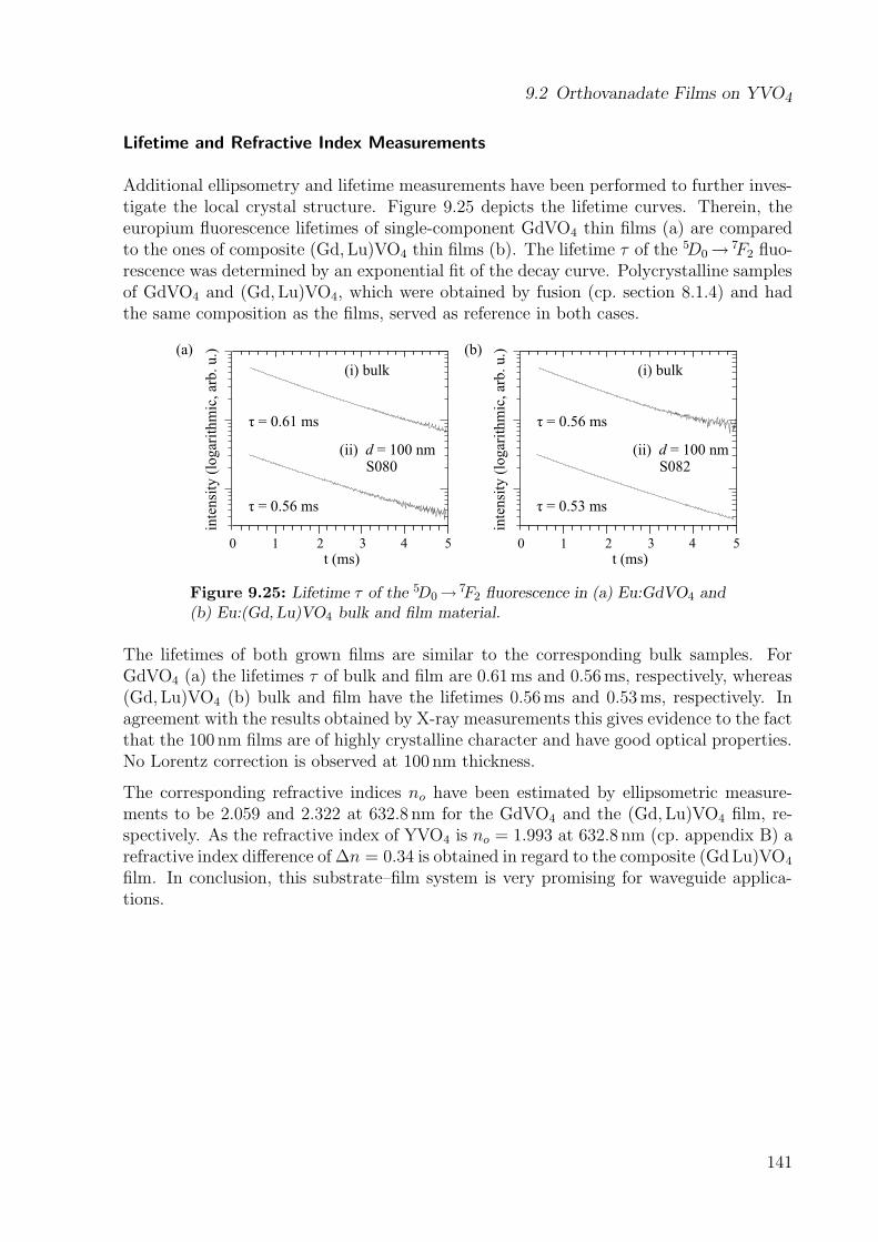
9.2 Orthovanadate Films on YVO4
Lifetime and Refractive Index Measurements
Additional ellipsometry and lifetime measurements have been performed to further inves-tigate the local crystal structure. Figure 9.25 depicts the lifetime curves. Therein, theeuropium fluorescence lifetimes of single-component GdVO4 thin films (a) are comparedto the ones of composite (Gd, Lu)VO4 thin films (b). The lifetime τ of the 5D0→ 7F2 fluo-rescence was determined by an exponential fit of the decay curve. Polycrystalline samplesof GdVO4 and (Gd, Lu)VO4, which were obtained by fusion (cp. section 8.1.4) and hadthe same composition as the films, served as reference in both cases.
(a)
0 1 4 52 3
t (ms)
inte
nsi
ty (
logar
ithm
ic, ar
b. u.)
ô = 0.61 ms
(i) bulk
(ii) = 100 nmd
S080
ô = 0.56 ms
0 1 4 52 3
t (ms)
inte
nsi
ty (
logar
ithm
ic, ar
b. u.)
ô = 0.56 ms
(i) bulk
(ii) = 100 nmd
S082
ô = 0.53 ms
(b)
Figure 9.25: Lifetime τ of the 5D0→ 7F2 fluorescence in (a) Eu:GdVO4 and(b) Eu:(Gd, Lu)VO4 bulk and film material.
The lifetimes of both grown films are similar to the corresponding bulk samples. ForGdVO4 (a) the lifetimes τ of bulk and film are 0.61ms and 0.56ms, respectively, whereas(Gd, Lu)VO4 (b) bulk and film have the lifetimes 0.56ms and 0.53ms, respectively. Inagreement with the results obtained by X-ray measurements this gives evidence to the factthat the 100 nm films are of highly crystalline character and have good optical properties.No Lorentz correction is observed at 100 nm thickness.
The corresponding refractive indices no have been estimated by ellipsometric measure-ments to be 2.059 and 2.322 at 632.8 nm for the GdVO4 and the (Gd, Lu)VO4 film, re-spectively. As the refractive index of YVO4 is no = 1.993 at 632.8 nm (cp. appendix B) arefractive index difference of ∆n = 0.34 is obtained in regard to the composite (GdLu)VO4
film. In conclusion, this substrate–film system is very promising for waveguide applica-tions.
141
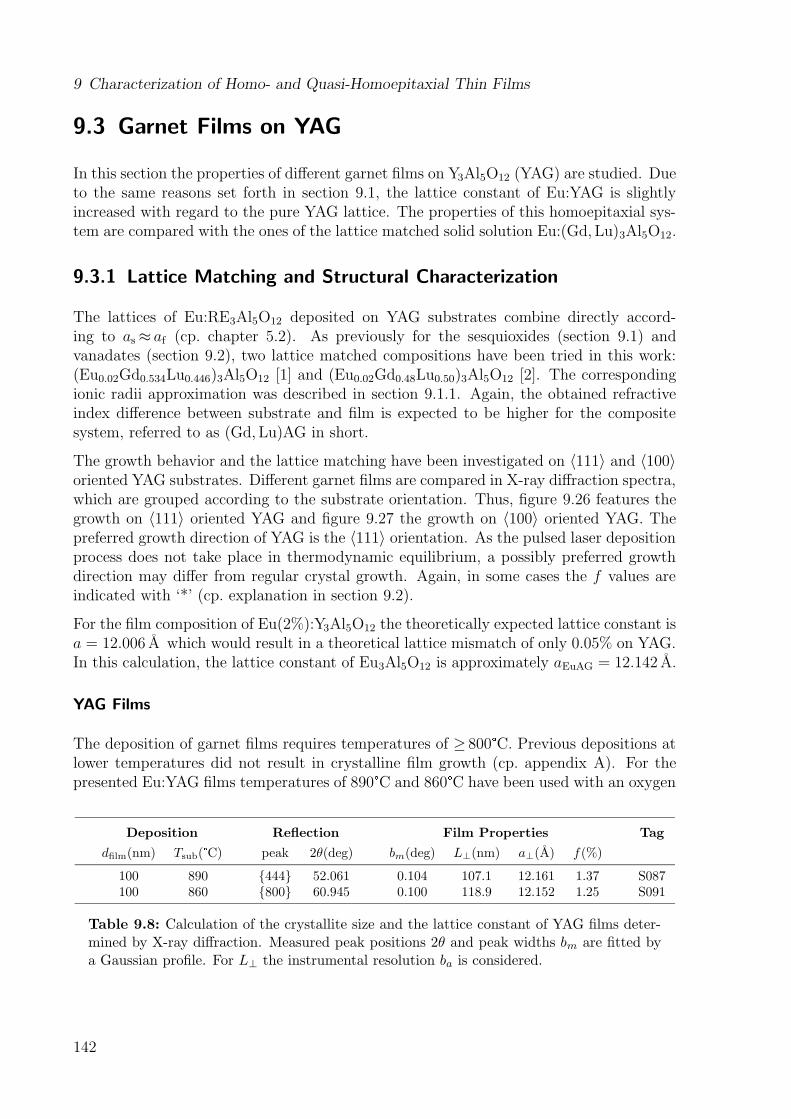
9 Characterization of Homo- and Quasi-Homoepitaxial Thin Films
9.3 Garnet Films on YAG
In this section the properties of different garnet films on Y3Al5O12 (YAG) are studied. Dueto the same reasons set forth in section 9.1, the lattice constant of Eu:YAG is slightlyincreased with regard to the pure YAG lattice. The properties of this homoepitaxial sys-tem are compared with the ones of the lattice matched solid solution Eu:(Gd, Lu)3Al5O12.
9.3.1 Lattice Matching and Structural Characterization
The lattices of Eu:RE3Al5O12 deposited on YAG substrates combine directly accord-ing to as≈ af (cp. chapter 5.2). As previously for the sesquioxides (section 9.1) andvanadates (section 9.2), two lattice matched compositions have been tried in this work:(Eu0.02Gd0.534Lu0.446)3Al5O12 [1] and (Eu0.02Gd0.48Lu0.50)3Al5O12 [2]. The correspondingionic radii approximation was described in section 9.1.1. Again, the obtained refractiveindex difference between substrate and film is expected to be higher for the compositesystem, referred to as (Gd, Lu)AG in short.
The growth behavior and the lattice matching have been investigated on 〈111〉 and 〈100〉oriented YAG substrates. Different garnet films are compared in X-ray diffraction spectra,which are grouped according to the substrate orientation. Thus, figure 9.26 features thegrowth on 〈111〉 oriented YAG and figure 9.27 the growth on 〈100〉 oriented YAG. Thepreferred growth direction of YAG is the 〈111〉 orientation. As the pulsed laser depositionprocess does not take place in thermodynamic equilibrium, a possibly preferred growthdirection may differ from regular crystal growth. Again, in some cases the f values areindicated with ‘*’ (cp. explanation in section 9.2).
For the film composition of Eu(2%):Y3Al5O12 the theoretically expected lattice constant isa = 12.006 A which would result in a theoretical lattice mismatch of only 0.05% on YAG.In this calculation, the lattice constant of Eu3Al5O12 is approximately aEuAG = 12.142 A.
YAG Films
The deposition of garnet films requires temperatures of ≥ 800 � C. Previous depositions atlower temperatures did not result in crystalline film growth (cp. appendix A). For thepresented Eu:YAG films temperatures of 890 � C and 860 � C have been used with an oxygen
Deposition Reflection Film Properties Tag
dfilm(nm) Tsub( � C) peak 2θ(deg) bm(deg) L⊥(nm) a⊥(A) f(%)
100 890 {444} 52.061 0.104 107.1 12.161 1.37 S087100 860 {800} 60.945 0.100 118.9 12.152 1.25 S091
Table 9.8: Calculation of the crystallite size and the lattice constant of YAG films deter-mined by X-ray diffraction. Measured peak positions 2θ and peak widths bm are fitted bya Gaussian profile. For L⊥ the instrumental resolution ba is considered.
142
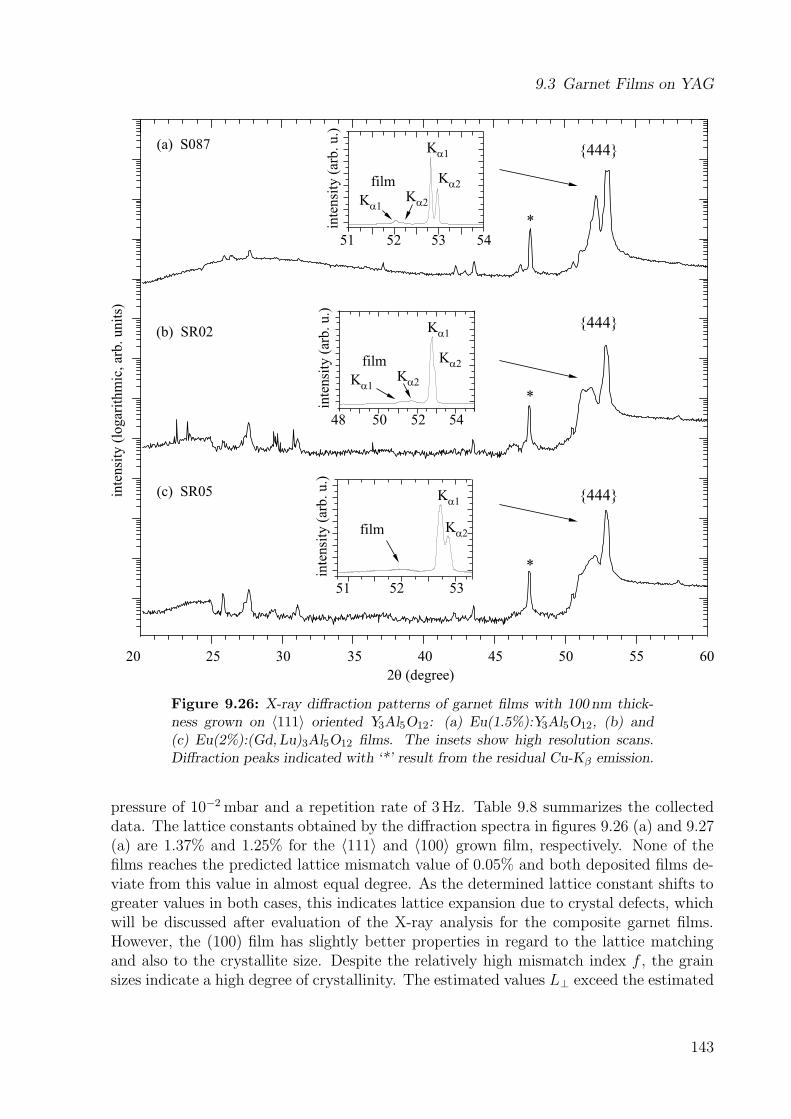
9.3 Garnet Films on YAG
inte
nsi
ty (
log
arit
hm
ic,
arb
. u
nit
s)
(a) S087
(b) SR02
(c) SR05
*
{444}
*
*
{444}
{444}
inte
nsi
ty (
arb
. u
.)
film
51 52 53 54
Ka2
Ka1
Ka2K
a1
inte
nsi
ty (
arb
. u
.)
film
48 50
Ka2
Ka1
Ka2K
a1
52 54
25 30 35 40 45 55 6020 50
2 (degree)q
inte
nsi
ty (
arb
. u
.)
film
51
Ka2
Ka1
52 53
Figure 9.26: X-ray diffraction patterns of garnet films with 100 nm thick-ness grown on 〈111〉 oriented Y3Al5O12: (a) Eu(1.5%):Y3Al5O12, (b) and(c) Eu(2%):(Gd, Lu)3Al5O12 films. The insets show high resolution scans.Diffraction peaks indicated with ‘*’ result from the residual Cu-Kβ emission.
pressure of 10−2mbar and a repetition rate of 3Hz. Table 9.8 summarizes the collecteddata. The lattice constants obtained by the diffraction spectra in figures 9.26 (a) and 9.27(a) are 1.37% and 1.25% for the 〈111〉 and 〈100〉 grown film, respectively. None of thefilms reaches the predicted lattice mismatch value of 0.05% and both deposited films de-viate from this value in almost equal degree. As the determined lattice constant shifts togreater values in both cases, this indicates lattice expansion due to crystal defects, whichwill be discussed after evaluation of the X-ray analysis for the composite garnet films.However, the (100) film has slightly better properties in regard to the lattice matchingand also to the crystallite size. Despite the relatively high mismatch index f , the grainsizes indicate a high degree of crystallinity. The estimated values L⊥ exceed the estimated
143
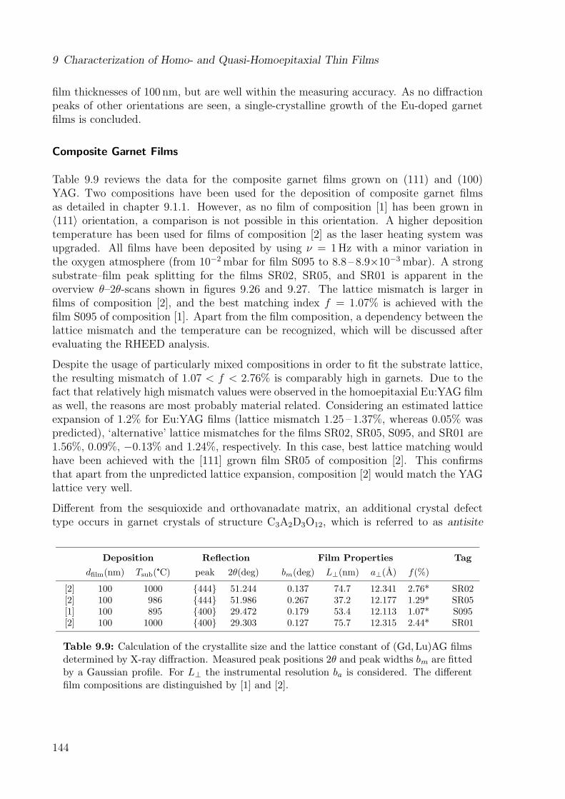
9 Characterization of Homo- and Quasi-Homoepitaxial Thin Films
film thicknesses of 100 nm, but are well within the measuring accuracy. As no diffractionpeaks of other orientations are seen, a single-crystalline growth of the Eu-doped garnetfilms is concluded.
Composite Garnet Films
Table 9.9 reviews the data for the composite garnet films grown on (111) and (100)YAG. Two compositions have been used for the deposition of composite garnet filmsas detailed in chapter 9.1.1. However, as no film of composition [1] has been grown in〈111〉 orientation, a comparison is not possible in this orientation. A higher depositiontemperature has been used for films of composition [2] as the laser heating system wasupgraded. All films have been deposited by using ν = 1Hz with a minor variation inthe oxygen atmosphere (from 10−2mbar for film S095 to 8.8 – 8.9×10⁻³mbar). A strongsubstrate–film peak splitting for the films SR02, SR05, and SR01 is apparent in theoverview θ–2θ-scans shown in figures 9.26 and 9.27. The lattice mismatch is larger infilms of composition [2], and the best matching index f = 1.07% is achieved with thefilm S095 of composition [1]. Apart from the film composition, a dependency between thelattice mismatch and the temperature can be recognized, which will be discussed afterevaluating the RHEED analysis.
Despite the usage of particularly mixed compositions in order to fit the substrate lattice,the resulting mismatch of 1.07 < f < 2.76% is comparably high in garnets. Due to thefact that relatively high mismatch values were observed in the homoepitaxial Eu:YAG filmas well, the reasons are most probably material related. Considering an estimated latticeexpansion of 1.2% for Eu:YAG films (lattice mismatch 1.25 – 1.37%, whereas 0.05% waspredicted), ‘alternative’ lattice mismatches for the films SR02, SR05, S095, and SR01 are1.56%, 0.09%, −0.13% and 1.24%, respectively. In this case, best lattice matching wouldhave been achieved with the [111] grown film SR05 of composition [2]. This confirmsthat apart from the unpredicted lattice expansion, composition [2] would match the YAGlattice very well.
Different from the sesquioxide and orthovanadate matrix, an additional crystal defecttype occurs in garnet crystals of structure C3A2D3O12, which is referred to as antisite
Deposition Reflection Film Properties Tag
dfilm(nm) Tsub( � C) peak 2θ(deg) bm(deg) L⊥(nm) a⊥(A) f(%)
[2] 100 1000 {444} 51.244 0.137 74.7 12.341 2.76* SR02[2] 100 986 {444} 51.986 0.267 37.2 12.177 1.29* SR05[1] 100 895 {400} 29.472 0.179 53.4 12.113 1.07* S095[2] 100 1000 {400} 29.303 0.127 75.7 12.315 2.44* SR01
Table 9.9: Calculation of the crystallite size and the lattice constant of (Gd, Lu)AG filmsdetermined by X-ray diffraction. Measured peak positions 2θ and peak widths bm are fittedby a Gaussian profile. For L⊥ the instrumental resolution ba is considered. The differentfilm compositions are distinguished by [1] and [2].
144
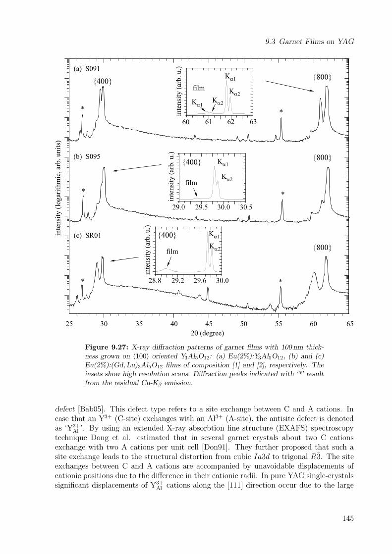
9.3 Garnet Films on YAG
inte
nsi
ty (
logar
ithm
ic, ar
b. unit
s)
*
(a) S091
(b) S095
(c) SR01
{800}
{800}
{800}
{400}
{400}
{400}
*
*
*
*
*
25 30 35 40 45 55 60 6550
2 (degree)q
inte
nsi
ty (
arb. u.)
film
60 61 62 63
Ka2
Ka1
Ka2K
a1
inte
nsi
ty (
arb. u.)
film
29.0 29.5 30.0 30.5
Ka2
Ka1
inte
nsi
ty (
arb. u.)
film
28.8 29.2 29.6 30.0
Ka2
Ka1
Figure 9.27: X-ray diffraction patterns of garnet films with 100 nm thick-ness grown on 〈100〉 oriented Y3Al5O12: (a) Eu(2%):Y3Al5O12, (b) and (c)Eu(2%):(Gd, Lu)3Al5O12 films of composition [1] and [2], respectively. Theinsets show high resolution scans. Diffraction peaks indicated with ‘*’ resultfrom the residual Cu-Kβ emission.
defect [Bab05]. This defect type refers to a site exchange between C and A cations. Incase that an Y3+ (C-site) exchanges with an Al3+ (A-site), the antisite defect is denotedas ‘Y3+
Al ’. By using an extended X-ray absorbtion fine structure (EXAFS) spectroscopytechnique Dong et al. estimated that in several garnet crystals about two C cationsexchange with two A cations per unit cell [Don91]. They further proposed that such asite exchange leads to the structural distortion from cubic Ia3d to trigonal R3. The siteexchanges between C and A cations are accompanied by unavoidable displacements ofcationic positions due to the difference in their cationic radii. In pure YAG single-crystalssignificant displacements of Y3+
Al cations along the [111] direction occur due to the large
145
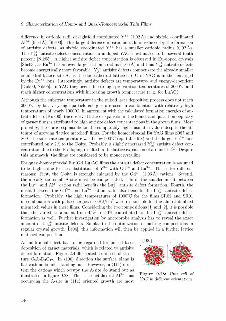
9 Characterization of Homo- and Quasi-Homoepitaxial Thin Films
difference in cationic radii of eightfold coordinated Y3+ (1.02 A) and sixfold coordinatedAl3+ (0.54 A) [She03]. This large difference in cationic radii is reduced by the formationof antisite defects, as sixfold coordinated Y3+ has a smaller cationic radius (0.92 A).The Y3+
Al antisite defect concentration in undoped YAG is estimated to be several tenthpercent [Nik05]. A higher antisite defect concentration is observed in Eu-doped crystals[She03], as Eu3+ has an even larger cationic radius (1.06 A) and thus Y3+
Al antisite defectsbecome energetically more favorable. Y3+
Al antisite defects compensate the already smalleroctahedral lattice site A, as the dodecahedral lattice site C in YAG is further enlargedby the Eu3+ ions. Interestingly, antisite defects are temperature- and energy-dependent[Kuk00, Nik05]. In YAG they occur due to high preparation temperatures of 2000 � C andreach higher concentrations with increasing growth temperature (e. g. for LuAG).
Although the substrate temperature in the pulsed laser deposition process does not reach2000 � C by far, very high particle energies are used in combination with relatively hightemperatures of nearly 1000 � C. In agreement with the calculated formation energies of an-tisite defects [Kuk00], the observed lattice expansion in the homo- and quasi-homoepitaxyof garnet films is attributed to high antisite defect concentrations in the grown films. Mostprobably, these are responsible for the comparably high mismatch values despite the at-tempt of growing ‘lattice matched’ films. For the homoepitaxial Eu:YAG films S087 andS091 the substrate temperature was below 900 � C (cp. table 9.8) and the larger Eu3+ ionscontributed only 2% to the C-site. Probably, a slightly increased Y3+
Al antisite defect con-centration due to the Eu-doping resulted in the lattice expansion of around 1.2%. Despitethis mismatch, the films are considered to be monocrystalline.
For quasi-homoepitaxial Eu:(Gd, Lu)AG films the antisite defect concentration is assumedto be higher due to the substitution of Y3+ with Gd3+ and Lu3+. This is for differentreasons: First, the C-site is strongly enlarged by the Gd3+ (1.06 A) cations. Second,the already too small A-site must be compensated. Third, the smaller misfit betweenthe Lu3+ and Al3+ cation radii benefits the Lu3+Al antisite defect formation. Fourth, themisfit between the Gd3+ and Lu3+ cation radii also benefits the Lu3+Al antisite defectformation. Probably, the high temperatures of 1000 � C for the films SR02 and SR01in combination with pulse energies of 0.8 J/cm2 were responsible for the almost doubledmismatch values in these films. Considering the two compositions [1] and [2], it is possiblethat the varied Lu-amount from 45% to 50% contributed to the Lu3+Al antisite defectformation as well. Further investigation by microprobe analysis has to reveal the exactamount of Lu3+Al antisite defects. Similar to the optimization of melting compositions inregular crystal growth [Ile04], this information will then be applied in a further lattice
[100] [111]
Figure 9.28: Unit cell ofYAG in different orientations
matched composition.
An additional effect has to be regarded for pulsed laserdeposition of garnet materials, which is related to antisitedefect formation. Figure 2.4 illustrated a unit cell of struc-ture C3A2D3O12. In 〈100〉 direction the surface plane isflat with no bonds ‘standing out’. However, in 〈111〉 direc-tion the cations which occupy the A-site do stand out asillustrated in figure 9.28. Thus, the octahedral Al3+ ionsoccupying the A-site in 〈111〉 oriented growth are most
146
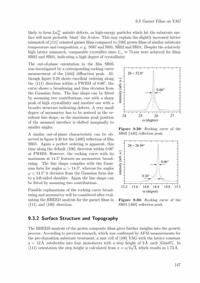
9.3 Garnet Films on YAG
likely to form Lu3+Al antisite defects, as high-energy particles which hit the substrate sur-face will most probably ‘blast’ the A-sites. This may explain the slightly increased latticemismatch of [111] oriented garnet films compared to [100] grown films of similar substratetemperature and composition, e. g. S087 and S091, SR02 and SR01. Despite the relativelyhigh lattice mismatch, comparable crystallite sizes L⊥ ≈ 75 nm were achieved for filmsSR02 and SR01, indicating a high degree of crystallinity.
inte
nsi
ty (
arb. u.)
2 = 52.0°q
24 25 26 27
w (degree)
0.06°
Figure 9.29: Rocking curve of theSR05 {444} reflection peak.
0.06°
inte
nsi
ty (
arb
. u
.)
2 = 28.99°q
13.2 14.0 14.8
w (degree)
13.6 14.4 15.2
0.26°
Figure 9.30: Rocking curve of theSR01 {400} reflection peak.
The out-of-plane orientation in the film SR05was investigated by a corresponding rocking curvemeasurement of the {444} diffraction peak. Al-though figure 9.29 shows excellent ordering alongthe 〈111〉 direction within a FWHM of 0.06 � , thecurve shows a broadening and thus deviates fromthe Gaussian form. The line shape can be fittedby assuming two contributions, one with a sharppeak of high crystallinity and another one with abroader structure indicating defects. A very smalldegree of asymmetry has to be noticed in the re-sultant line shape, as the maximum peak positionof the assumed interface is shifted marginally tosmaller angles.
A similar out-of-plane characteristic can be ob-served in figure 9.30 for the {400} reflection of filmSR01. Again a perfect ordering is apparent, thistime along the default 〈100〉 direction within 0.06 �at FWHM. However, the rocking curve with itsmaximum at 14.5 � features an asymmetric broad-ening. The line shape complies with the Gaus-sian form for angles ω > 14.5 � , whereas for anglesω < 14.5 � it deviates from the Gaussian form dueto a left-sided shoulder. Again the line shape canbe fitted by assuming two contributions.
Possible explanations of the rocking curve broad-ening and asymmetry will be considered after eval-uating the RHEED analysis for the garnet films in〈111〉 and 〈100〉 direction.
9.3.2 Surface Structure and Topography
The RHEED analysis of the grown composite films gives further insights into the growthprocess. According to previous research, which was confirmed by AFM measurements forthe pre-deposition substrate treatment, a unit cell of [100] YAG with the lattice constanta = 12 A subdivides into four monolayers with a step height of 3 A each [Gun07]. In〈111〉 orientation the step height is calculated from x = a/4
√3, which results in 1.73 A.
147
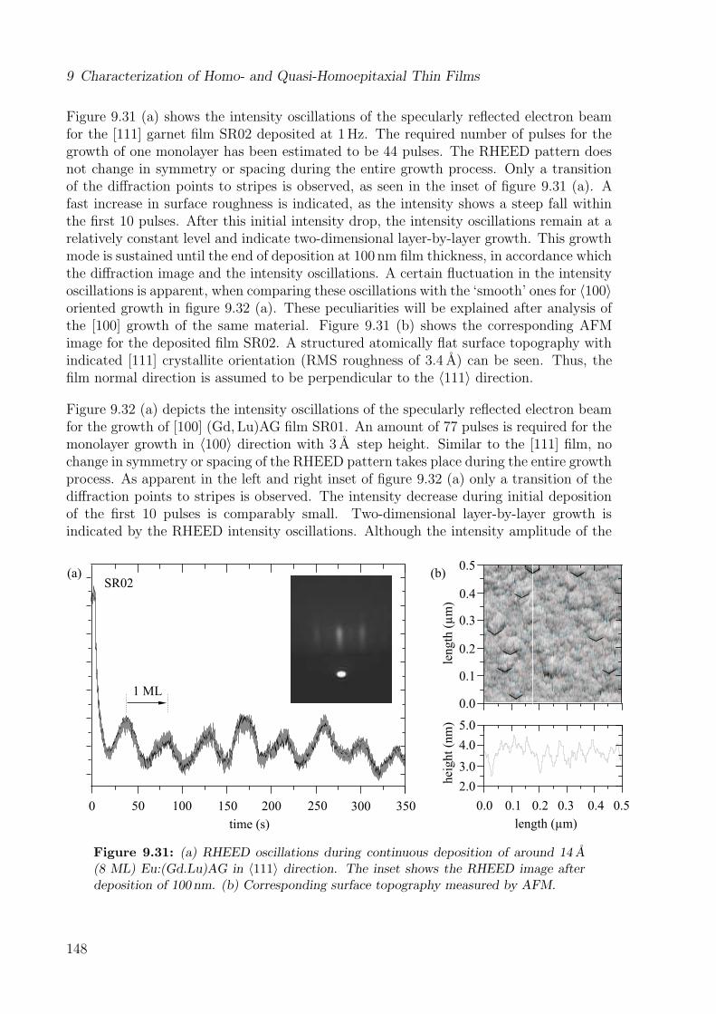
9 Characterization of Homo- and Quasi-Homoepitaxial Thin Films
Figure 9.31 (a) shows the intensity oscillations of the specularly reflected electron beamfor the [111] garnet film SR02 deposited at 1Hz. The required number of pulses for thegrowth of one monolayer has been estimated to be 44 pulses. The RHEED pattern doesnot change in symmetry or spacing during the entire growth process. Only a transitionof the diffraction points to stripes is observed, as seen in the inset of figure 9.31 (a). Afast increase in surface roughness is indicated, as the intensity shows a steep fall withinthe first 10 pulses. After this initial intensity drop, the intensity oscillations remain at arelatively constant level and indicate two-dimensional layer-by-layer growth. This growthmode is sustained until the end of deposition at 100 nm film thickness, in accordance whichthe diffraction image and the intensity oscillations. A certain fluctuation in the intensityoscillations is apparent, when comparing these oscillations with the ‘smooth’ ones for 〈100〉oriented growth in figure 9.32 (a). These peculiarities will be explained after analysis ofthe [100] growth of the same material. Figure 9.31 (b) shows the corresponding AFMimage for the deposited film SR02. A structured atomically flat surface topography withindicated [111] crystallite orientation (RMS roughness of 3.4 A) can be seen. Thus, thefilm normal direction is assumed to be perpendicular to the 〈111〉 direction.
Figure 9.32 (a) depicts the intensity oscillations of the specularly reflected electron beamfor the growth of [100] (Gd, Lu)AG film SR01. An amount of 77 pulses is required for themonolayer growth in 〈100〉 direction with 3 A step height. Similar to the [111] film, nochange in symmetry or spacing of the RHEED pattern takes place during the entire growthprocess. As apparent in the left and right inset of figure 9.32 (a) only a transition of thediffraction points to stripes is observed. The intensity decrease during initial depositionof the first 10 pulses is comparably small. Two-dimensional layer-by-layer growth isindicated by the RHEED intensity oscillations. Although the intensity amplitude of the
0 50 100 150 200 300 350250
time (s)
(b)
0.0 0.1 0.2 0.3 0.4 0.5
length ( m)µ
len
gth
(m
)µ
hei
gh
t (n
m)
0.0
0.1
0.2
0.3
0.4
0.5
2.0
3.0
4.0
5.0
(a)
1 ML
SR02
Figure 9.31: (a) RHEED oscillations during continuous deposition of around 14 A(8 ML) Eu:(Gd.Lu)AG in 〈111〉 direction. The inset shows the RHEED image afterdeposition of 100 nm. (b) Corresponding surface topography measured by AFM.
148
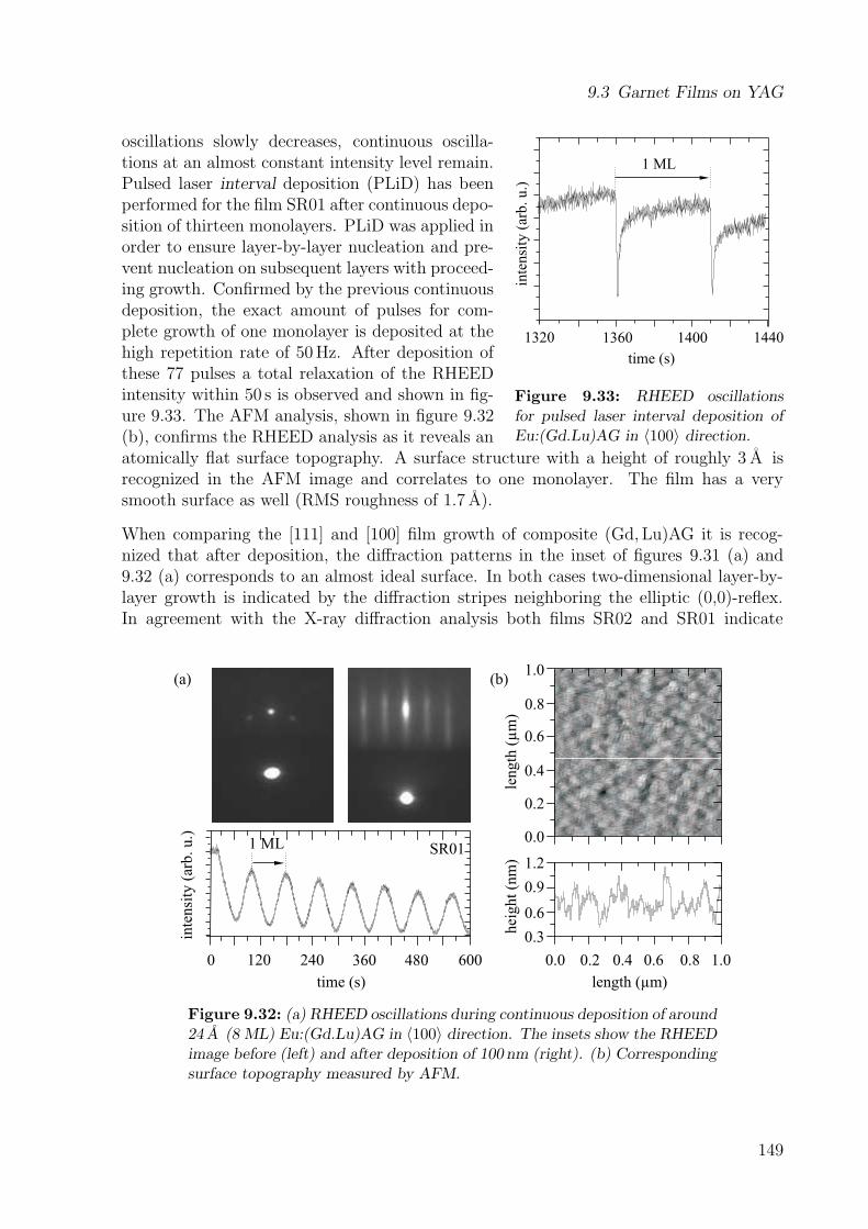
9.3 Garnet Films on YAG
inte
nsi
ty (
arb
. u
.)
1320 1360 1400 1440
time (s)
1 ML
Figure 9.33: RHEED oscillationsfor pulsed laser interval deposition ofEu:(Gd.Lu)AG in 〈100〉 direction.
oscillations slowly decreases, continuous oscilla-tions at an almost constant intensity level remain.Pulsed laser interval deposition (PLiD) has beenperformed for the film SR01 after continuous depo-sition of thirteen monolayers. PLiD was applied inorder to ensure layer-by-layer nucleation and pre-vent nucleation on subsequent layers with proceed-ing growth. Confirmed by the previous continuousdeposition, the exact amount of pulses for com-plete growth of one monolayer is deposited at thehigh repetition rate of 50Hz. After deposition ofthese 77 pulses a total relaxation of the RHEEDintensity within 50 s is observed and shown in fig-ure 9.33. The AFM analysis, shown in figure 9.32(b), confirms the RHEED analysis as it reveals anatomically flat surface topography. A surface structure with a height of roughly 3 A isrecognized in the AFM image and correlates to one monolayer. The film has a verysmooth surface as well (RMS roughness of 1.7 A).
When comparing the [111] and [100] film growth of composite (Gd, Lu)AG it is recog-nized that after deposition, the diffraction patterns in the inset of figures 9.31 (a) and9.32 (a) corresponds to an almost ideal surface. In both cases two-dimensional layer-by-layer growth is indicated by the diffraction stripes neighboring the elliptic (0,0)-reflex.In agreement with the X-ray diffraction analysis both films SR02 and SR01 indicate
inte
nsi
ty (
arb
. u
.)
0 120 240 360
time (s)
480 600
(a) (b)
0.0 0.2 0.4 0.6 0.8 1.0
length ( m)µ
len
gth
(m
)µ
hei
gh
t (n
m)
0.0
0.2
0.4
0.6
0.8
1.0
0.3
0.6
0.9
1.2
1 ML SR01
Figure 9.32: (a) RHEED oscillations during continuous deposition of around24 A (8 ML) Eu:(Gd.Lu)AG in 〈100〉 direction. The insets show the RHEEDimage before (left) and after deposition of 100 nm (right). (b) Correspondingsurface topography measured by AFM.
149
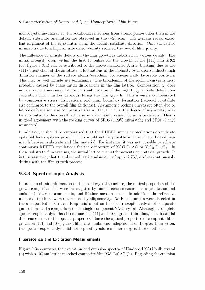
9 Characterization of Homo- and Quasi-Homoepitaxial Thin Films
monocrystalline character. No additional reflections from atomic planes other than in thedefault substrate orientation are observed in the θ–2θ-scan. The ω-scans reveal excel-lent alignment of the crystallites along the default substrate direction. Only the latticemismatch due to a high antisite defect density reduced the overall film quality.
The influence of antisite defects on the film growth is indicated in various details. Theinitial intensity drop within the first 10 pulses for the growth of the [111] film SR02(cp. figure 9.31a) can be attributed to the above mentioned A-site ‘blasting’ due to the〈111〉 orientation of the substrate. Fluctuations in the intensity oscillations indicate highdiffusion energies of the surface atoms ‘searching’ for energetically favorable positions.This may as well include site exchanging. The broadening of the rocking curves is mostprobably caused by these initial dislocations in the film lattice. Composition [2] doesnot deliver the necessary lattice constant because of the high Lu3+Al antisite defect con-centration which further develops during the film growth. This is surely compensatedby compressive stress, dislocations, and grain boundary formation (reduced crystallitesize compared to the overall film thickness). Asymmetric rocking curves are often due tolattice deformation and compressive strain [Hag01]. Thus, the degree of asymmetry maybe attributed to the overall lattice mismatch mainly caused by antisite defects. This isin good agreement with the rocking curves of SR05 (1.29% mismatch) and SR01 (2.44%mismatch).
In addition, it should be emphasized that the RHEED intensity oscillations do indicateepitaxial layer-by-layer growth. This would not be possible with an initial lattice mis-match between substrate and film material. For instance, it was not possible to achievecontinuous RHEED oscillations for the deposition of YAG–LuAG or Y2O3–Lu2O3. Inthese substrate–film systems, the initial lattice mismatch prevents an epitaxial growth. Itis thus assumed, that the observed lattice mismatch of up to 2.76% evolves continuouslyduring with the film growth process.
9.3.3 Spectroscopic Analysis
In order to obtain information on the local crystal structure, the optical properties of thegrown composite films were investigated by luminescence measurements (excitation andemission), VUV measurements, and lifetime measurements. In addition, the refractiveindices of the films were determined by ellipsometry. No Eu-impurities were detected inthe undeposited substrates. Emphasis is put on the spectroscopic analysis of compositegarnet films and a comparison to the single-component YAG crystal. Although a completespectroscopic analysis has been done for [111] and [100] grown thin films, no substantialdifferences exist in the optical properties. Since the optical properties of composite filmsgrown on [111] and [100] garnet films are similar and independent of the growth direction,the spectroscopic analysis did not separately address different growth orientations.
Fluorescence and Excitation Measurements
Figure 9.34 compares the excitation and emission spectra of Eu-doped YAG bulk crystal(a) with a 100 nm lattice matched composite film (Gd, Lu)AG (b). Regarding the emission
150
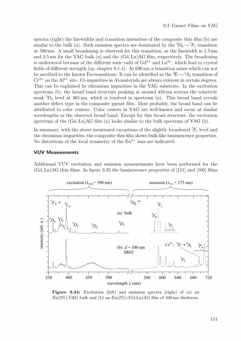
9.3 Garnet Films on YAG
spectra (right) the linewidths and transition intensities of the composite thin film (b) aresimilar to the bulk (a). Both emission spectra are dominated by the 5D0→ 7F1 transitionat 590 nm. A small broadening is observed for this transition, as the linewidth is 1.5 nmand 2.5 nm for the YAG bulk (a) and the (Gd, Lu)AG film, respectively. The broadeningis understood because of the different ionic radii of Gd3+ and Lu3+, which lead to crystalfields of different strength (cp. chapter 8.1.4). At 696 nm a transition arises which can notbe ascribed to the known Eu-transitions. It can be identified as the 2E→ 4A2 transition ofCr3+ on the Al3+ site. Cr-impurities in Al-materials are always existent in certain degrees.This can be explained by chromium impurities in the YAG substrate. In the excitationspectrum (b), the broad band structure peaking at around 458 nm screens the relativelyweak 5D2 level at 465 nm, which is resolved in spectrum (a). This broad band revealsanother defect type in the composite garnet film. Most probably, the broad band can beattributed to color centers. Color centers in YAG are well-known and occur at similarwavelengths as the observed broad band. Except for this broad structure, the excitationspectrum of the (Gd, Lu)AG film (a) looks similar to the bulk spectrum of YAG (b).
In summary, with the above mentioned exceptions of the slightly broadened 7F1 level andthe chromium impurities, the composite thin film shows bulk-like luminescence properties.No distortions of the local symmetry of the Eu3+ ions are indicated.
VUV Measurements
Additional VUV excitation and emission measurements have been performed for the(Gd, Lu)AG thin films. In figure 9.35 the luminescence properties of [111] and [100] films
wavelength (nm)l
350 400 450 600 640 680 720
(a) bulk
(b) d = 100 nmSR02
inte
nsi
ty (
arb. u.)
excitation ( = 590 nm)lem emission ( = 275 nm)lex
560
5D1
7F0
5D2
5D3
5L 6
5GJ
5D4
500
7F2
®5D0
7F3
7F4
®7F0 7
F1
®2E
4A2
3+Cr :
Figure 9.34: Excitation (left) and emission spectra (right) of (a) anEu(2%):YAG bulk and (b) an Eu(2%):(Gd,Lu)AG film of 100 nm thickness.
151
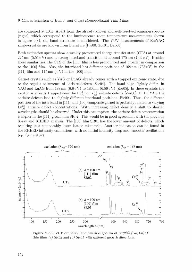
9 Characterization of Homo- and Quasi-Homoepitaxial Thin Films
are compared at 10K. Apart from the already known and well-resolved emission spectra(right), which correspond to the luminescence room temperature measurements shownin figure 9.34, the band structure is considered. The VUV measurements of Eu:YAGsingle-crystals are known from literature [Pie00, Zor04, Bab05].
Both excitation spectra show a weakly pronounced charge transfer state (CTS) at around225 nm (5.51 eV) and a strong interband transition at around 175 nm (7.09 eV). Besidesthese similarities, the CTS of the [111] film is less pronounced and broader in comparisonto the [100] film. Also, the interband has different positions of 168 nm (738 eV) in the[111] film and 175 nm ( eV) in the [100] film.
Garnet crystals such as YAG or LuAG already comes with a trapped excitonic state, dueto the regular occurrence of antisite defects [Zor04]. The band edge slightly differs inYAG and LuAG from 188 nm (6.6 eV) to 180 nm (6.89 eV) [Zor05]. In these crystals theexciton is already trapped near the Lu3+Al or Y3+
Al antisite defects [Zor06]. In Eu:YAG theantisite defects lead to slightly different interband positions [Pie00]. Thus, the differentposition of the interband in [111] and [100] composite garnet is probably related to varyingLu3+Al antisite defect concentrations. With increasing defect density a shift to shorterwavelengths should be observed. Under this assumption, the antisite defect concentrationis higher in the [111] grown film SR02. This would be in good agreement with the previousX-ray and RHEED analysis. The [100] film SR01 has the lower amount of defects, whichresulting in a comparably lower lattice mismatch. Another indication can be found inthe RHEED intensity oscillations, with no initial intensity drop and ‘smooth’ oscillations(cp. figure 9.32).
CTS
7F0
7F2 7
F3
7F4
7F1
100 150 200 250 300 600 640 680 760
wavelength (nm)l
inte
nsi
ty (
arb
. u
.)
excitation ( = 590 nm)lem emission ( = 166 nm)lex
720
7F5CTS
(a) = 100 nm[111] filmSR02
d
(b) = 100 nm[100] filmSR01
d
®2 E
4 A2
3+Cr
3+Cr
®5D0
Figure 9.35: VUV excitation and emission spectra of Eu(2%):(Gd, Lu)AGthin films (a) SR02 and (b) SR01 with different growth directions.
152
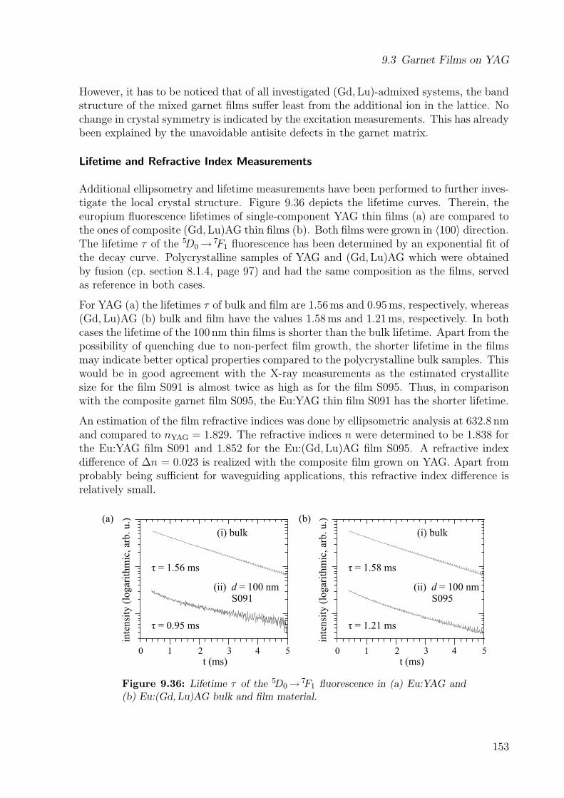
9.3 Garnet Films on YAG
However, it has to be noticed that of all investigated (Gd, Lu)-admixed systems, the bandstructure of the mixed garnet films suffer least from the additional ion in the lattice. Nochange in crystal symmetry is indicated by the excitation measurements. This has alreadybeen explained by the unavoidable antisite defects in the garnet matrix.
Lifetime and Refractive Index Measurements
Additional ellipsometry and lifetime measurements have been performed to further inves-tigate the local crystal structure. Figure 9.36 depicts the lifetime curves. Therein, theeuropium fluorescence lifetimes of single-component YAG thin films (a) are compared tothe ones of composite (Gd, Lu)AG thin films (b). Both films were grown in 〈100〉 direction.The lifetime τ of the 5D0→ 7F1 fluorescence has been determined by an exponential fit ofthe decay curve. Polycrystalline samples of YAG and (Gd, Lu)AG which were obtainedby fusion (cp. section 8.1.4, page 97) and had the same composition as the films, servedas reference in both cases.
For YAG (a) the lifetimes τ of bulk and film are 1.56ms and 0.95ms, respectively, whereas(Gd, Lu)AG (b) bulk and film have the values 1.58ms and 1.21ms, respectively. In bothcases the lifetime of the 100 nm thin films is shorter than the bulk lifetime. Apart from thepossibility of quenching due to non-perfect film growth, the shorter lifetime in the filmsmay indicate better optical properties compared to the polycrystalline bulk samples. Thiswould be in good agreement with the X-ray measurements as the estimated crystallitesize for the film S091 is almost twice as high as for the film S095. Thus, in comparisonwith the composite garnet film S095, the Eu:YAG thin film S091 has the shorter lifetime.
An estimation of the film refractive indices was done by ellipsometric analysis at 632.8 nmand compared to nYAG = 1.829. The refractive indices n were determined to be 1.838 forthe Eu:YAG film S091 and 1.852 for the Eu:(Gd, Lu)AG film S095. A refractive indexdifference of ∆n = 0.023 is realized with the composite film grown on YAG. Apart fromprobably being sufficient for waveguiding applications, this refractive index difference isrelatively small.
(a)
0 1 4 52 3
t (ms)
inte
nsi
ty (
logar
ithm
ic, ar
b. u.)
ô = 1.56 ms
(i) bulk
(ii) = 100 nmS091d
ô = 0.95 ms
0 1 4 52 3
t (ms)
inte
nsi
ty (
logar
ithm
ic, ar
b. u.)
ô = 1.58 ms
(i) bulk
(ii) = 100 nmS095d
ô = 1.21 ms
(b)
Figure 9.36: Lifetime τ of the 5D0→ 7F1 fluorescence in (a) Eu:YAG and(b) Eu:(Gd, Lu)AG bulk and film material.
153
9 Characterization of Homo- and Quasi-Homoepitaxial Thin Films
9.4 Summary and Discussion
Lattice matching of homo- and quasi-homoepitaxial films grown on Y2O3, YVO4, andY3Al5O12 substrate materials has been investigated by using the pulsed laser depositiontechnique. The film growth behavior in the different crystal orientations 〈111〉 and 〈100〉has been considered for sesquioxides and garnets. Except for the composite garnet films,the ionic radii approximation delivered good lattice matching of > 99.5%.
Sesquioxide Films on Yttria
High substrate temperatures of 900 – 1000 � C are required in order to realize lattice matchedsesquioxide films of high crystallinity. Considering the estimated crystallite sizes in rela-tion to the deposition temperature, Lu2O3 films require even higher temperatures thanmixed (Gd, Lu)2O3 films. By using the solid solution (Gd, Lu)2O3 of composition [2],lattice matching of 99.54% has been achieved.
In general, the optical properties of the mixed sesquioxide films have bulk-like character.Only a marginal broadening of transition linewidths is observed for (Gd, Lu)2O3 filmscompared to single-component Y2O3 bulk crystals. However, a certain disturbance of thecrystal structure was recognized by VUV excitation measurements. This is due to theadditional ion, which also occupies the C2 and C3i sites in the sesquioxide matrix andresults in less structured ES and CTS in the VUV excitation spectra.
Slightly tilted, highly crystalline film growth is indicated by X-ray rocking curve analysis.Probably, the tilting occurs in order to compensate stress while preserving the lateralcross-linking of the film lattice. The stress may arise because of the residual lattice mis-match. Further investigation of the in-plane lattice properties (collateral cross-linking,lattice constant a‖, and crystallite size L‖) by surface X-ray diffraction (SXRD) are re-quired. The exact distribution of the Gd-, Lu-, and Eu-atoms could be investigated byhigh-resolution transmission electron microscopy (HRTEM). The exact determination offilm stress by these techniques is crucial in order to discern whether the remaining latticemismatch is due to lattice expansion. Otherwise, the (Gd, Lu)-mixing has to be furtherimproved.
Another influential factor is the miscut angle of the sesquioxide substrates, as it maybe responsible for varying lattice matching success at identical conditions [Joy88, Rij04,Gun07]. For instance, the miscut angles β for the Y2O3 [100] substrates of SR03, SR04,and SR10 have been β > 1.5 � each. These are comparably high miscut values, as epitaxialgrade polished commercial α-Al2O3 and YAG substrates had much smaller miscut angles.In comparison, the miscut of the α-Al2O3 substrate shown in figure 6.5 (b) is determinedto be β=0.005 � . Step-bunching and uneven surfaces (tension) have been observed forthese substrates, potentially affecting the growth process.
Although slightly better lattice matching has been obtained by [100] grown films, no def-inite preference in growth direction could be investigated. A reason can be found in thevarying substrate quality, which levels out a better growth behavior. With better orientedsubstrates, this analysis can be done by investigating the RHEED intensity oscillation de-
154
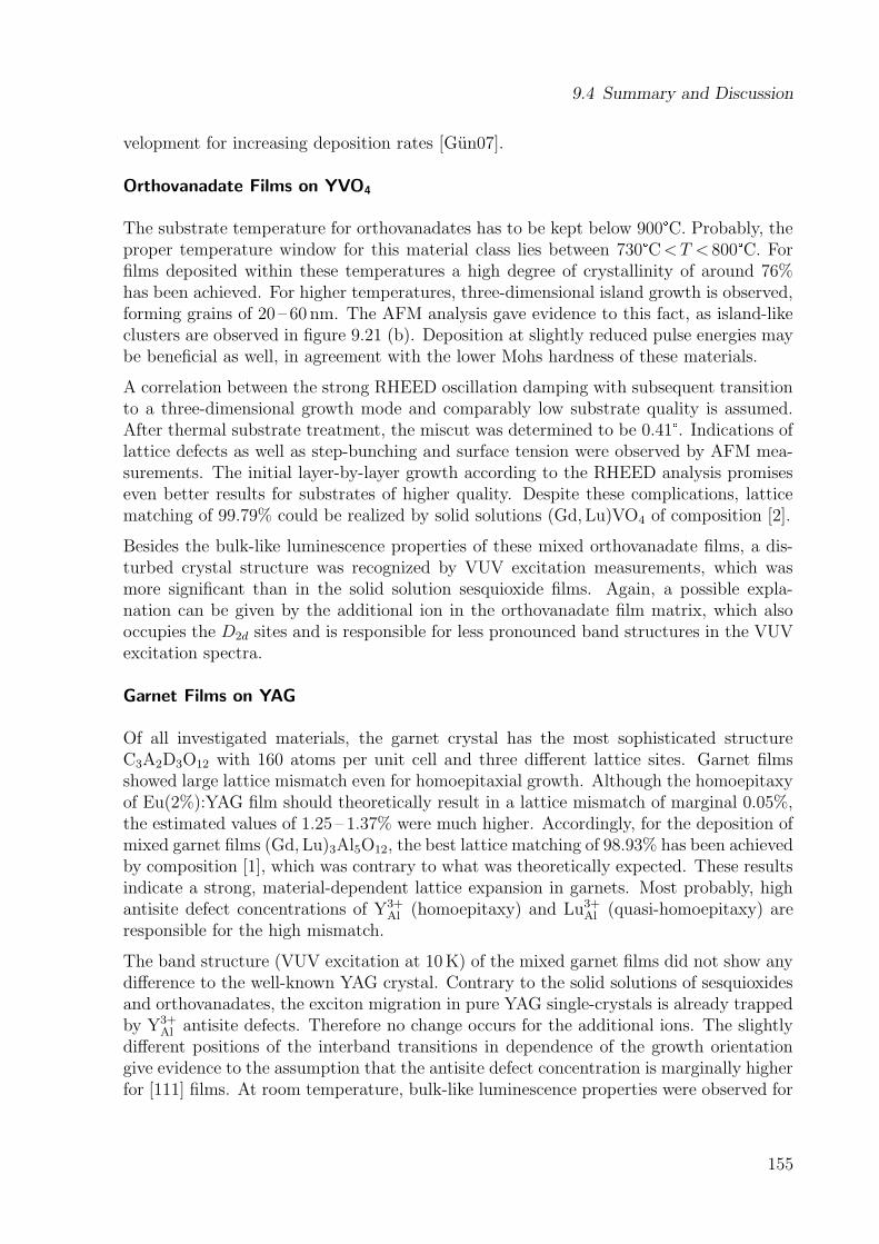
9.4 Summary and Discussion
velopment for increasing deposition rates [Gun07].
Orthovanadate Films on YVO4
The substrate temperature for orthovanadates has to be kept below 900 � C. Probably, theproper temperature window for this material class lies between 730 � C<T < 800 � C. Forfilms deposited within these temperatures a high degree of crystallinity of around 76%has been achieved. For higher temperatures, three-dimensional island growth is observed,forming grains of 20 – 60 nm. The AFM analysis gave evidence to this fact, as island-likeclusters are observed in figure 9.21 (b). Deposition at slightly reduced pulse energies maybe beneficial as well, in agreement with the lower Mohs hardness of these materials.
A correlation between the strong RHEED oscillation damping with subsequent transitionto a three-dimensional growth mode and comparably low substrate quality is assumed.After thermal substrate treatment, the miscut was determined to be 0.41 � . Indications oflattice defects as well as step-bunching and surface tension were observed by AFM mea-surements. The initial layer-by-layer growth according to the RHEED analysis promiseseven better results for substrates of higher quality. Despite these complications, latticematching of 99.79% could be realized by solid solutions (Gd, Lu)VO4 of composition [2].
Besides the bulk-like luminescence properties of these mixed orthovanadate films, a dis-turbed crystal structure was recognized by VUV excitation measurements, which wasmore significant than in the solid solution sesquioxide films. Again, a possible expla-nation can be given by the additional ion in the orthovanadate film matrix, which alsooccupies the D2d sites and is responsible for less pronounced band structures in the VUVexcitation spectra.
Garnet Films on YAG
Of all investigated materials, the garnet crystal has the most sophisticated structureC3A2D3O12 with 160 atoms per unit cell and three different lattice sites. Garnet filmsshowed large lattice mismatch even for homoepitaxial growth. Although the homoepitaxyof Eu(2%):YAG film should theoretically result in a lattice mismatch of marginal 0.05%,the estimated values of 1.25 – 1.37% were much higher. Accordingly, for the deposition ofmixed garnet films (Gd, Lu)3Al5O12, the best lattice matching of 98.93% has been achievedby composition [1], which was contrary to what was theoretically expected. These resultsindicate a strong, material-dependent lattice expansion in garnets. Most probably, highantisite defect concentrations of Y3+
Al (homoepitaxy) and Lu3+Al (quasi-homoepitaxy) areresponsible for the high mismatch.
The band structure (VUV excitation at 10K) of the mixed garnet films did not show anydifference to the well-known YAG crystal. Contrary to the solid solutions of sesquioxidesand orthovanadates, the exciton migration in pure YAG single-crystals is already trappedby Y3+
Al antisite defects. Therefore no change occurs for the additional ions. The slightlydifferent positions of the interband transitions in dependence of the growth orientationgive evidence to the assumption that the antisite defect concentration is marginally higherfor [111] films. At room temperature, bulk-like luminescence properties were observed for
155
9 Characterization of Homo- and Quasi-Homoepitaxial Thin Films
the mixed garnet films. Further research is necessary to resolve the difficulties of latticematching in garnets. By microprobe analysis the exact lattice site distributions need to beinvestigated, which is done similarly for bulk single-crystals [Ile04]. This allows a garnet-specific (Eu,Gd, Lu) composition, in which the antisite defects are already considered.By adjusting the parameters of pulse energy and substrate temperature the formationenergies of antisite defects should not be reached during deposition. This presupposesa compromise between substrate temperatures required for highly crystalline films andsubstrate temperatures beneficial for antisite defect formation.
9.4.1 Lattice Defects and Lattice Expansion
Lattice expansion was observed in many of the deposited films. This has been attributedto possible lattice defects. As various defect types are known in literature, it is difficultto define the exact defect type and concentration in the grown films. Crystal defectcategories are point defects (vacancies, antisite defects), line defects (different types ofdislocations), planar defects (grain boundaries, antiphase boundaries), and bulk defects
(voids, impurities) [Kle89]. Thereof, point defects are the most likely ones to occur duringpulsed laser deposition.
These are defects which are not extended spatially in any dimension. Although no definedsize limitation is given for point defects, the term is typically used for defects involvingextra or missing atoms. In contrast to larger defects in an ordered structure (dislocations),the defective positions have no ordered structure. For historical reasons, various pointdefects are called ‘centers’, e. g. a vacancy in ionic solids is termed ‘F-center’ (color center).Figure 9.37 illustrates some typical point defect types. Bal et al. investigated the influenceof various point defects on the crystal lattice in KCl [Bal67]. Vacancies and interstitialions resulted in lattice expansion. It was observed that F-centers (vacancies, also calledSchottky defects) in additively colored KCl caused a lattice expansion of ∆v/v = 0.58per F-center. F-centers in X-irradiated KCl with the corresponding atoms displaced tointerstitial lattice sites (Frenkel pairs) caused a lattice expansion of ∆v/v = 1.15 perF-center. The increasing lattice constant is calculated from ∆a/a = − cot θ · ∆θ. Theinvestigated increase for KCl was ∆a/a=3– 5×10⁻⁵.Except for the garnet films with additional antisite defects, the lattice constant deviation∆a/a for the lattice matched films was usually between 0.002 – 0.01. Therefore, the defect
vacancyFrenkel pair
substitutional larger atom
substitutional smaller atom interstitial
Figure 9.37: Different point defects in amonatomic solid.
concentration of vacancies and intersti-tial ions in the grown lattice matchedfilms would be two orders of magni-tude higher. Most likely, other defecttypes also contribute to the lattice con-stant increase. Further research on de-fect types and concentrations in the de-posited films is necessary, including thegrowth of reference bulk single-crystalsof the solid solutions for comparisonpurposes.
156
10 Conclusions
10.1 Summary of Results
The subject of this thesis was the preparation and characterization of lattice matchedcrystalline rare-earth-doped oxide films for application as active or passive waveguidesand optical coatings. A summary of the presented work is given in this chapter.
Lattice Matched Substrate–Film Systems
Sesquioxide, orthovanadate and aluminum garnet films were prepared because each mate-rial class offers a number of advantageous mechanical and thermal properties (high meltingpoint, high Mohs hardness, low phonon energy, high thermal conductivity), which makesthem appropriate and recommendable for integrated optical devices. Sesquioxides, ortho-vanadates and aluminum garnets are well-known hosts for rare-earth-doped luminescencematerials (e. g. Eu:Y2O3 as red phosphor) and solid-state lasers (e. g. Yb:Lu2O3, Yb:YVO4,Nd:YAG). An exception was the preparation of Al2O3 films doped with chromium instead.Cr:Al2O3 is known to be the first solid-state laser material [Mai60].
Proper substrates for lattice matching were found in α-Al2O3, sesquioxide materials(Y2O3 and ScLuO3), YVO4, YAG, and LiYF4. Different possibilities of lattice matchingwere investigated by heteroepitaxy of Al2O3–ScLuO3 and LiYF4–Lu2O3 and by (quasi-)homoepitaxy of Y2O3–RE2O3, YVO4–REVO4 and YAG–REAG substrate–film systems.The lattice matching in the quasi-homoepitaxial systems was realized by mixing the(Eu,Gd, Lu)-amount to match the yttrium-based substrate material. Besides the latticematching purpose this also delivered a higher refractive index difference to the substrate.In the heteroepitaxial systems the achievable refractive index difference (0.15 < ∆n < 0.5at 1 � m) is still higher compared to (quasi-)homoepitaxial systems (∆n ≤ 0.04 at 1 � m).The film growth on Y2O3 and YAG was investigated in 〈111〉 and 〈100〉 direction.
Preparation
All films were fabricated by the pulsed laser deposition technique. Either pressed andsintered high purity powders or polycrystalline bulk materials obtained by fusion wereused as targets in the ablation experiments. The density of the sintered targets was about90% of the single-crystal density and no difference in the deposited films was noticed
157
10 Conclusions
in dependence of the used target type (sintered or crystalline). In the latter stage ofthis thesis, pre-deposition substrate annealing was performed to allow proper RHEEDmeasurements and obtain additional information on the substrates. By this treatment,reconstructed atomically flat surfaces were obtained, with visible terraces by which themonolayer step height could be determined. Varying miscut angles of β ≤ 2.58 � weredetermined.
An KrF excimer laser of 248 nm wavelength and 20 ns pulse duration was used for targetablation with material dependent laser fluences of 1.1 – 2.5 J/cm2. This resulted in ma-terial related growth rates of 0.002 – 0.01 A per pulse. The material-dependent thresholdfluence was determined for ablation from sintered and crystalline targets. In order toreduce a possible droplet formation, a large ablation spot of 5 – 7mm2 was used. Withmaterial dependent optimized deposition parameters crystalline film growth was achieved.
Structural Characterization
A number of analytical techniques were applied for a thorough characterization of the thinfilms. The structural analysis includes in-situ reflection high-energy electron diffraction(RHEED), ex-situ X-ray diffraction (XRD) and ex-situ atomic force microscopy (AFM).
Two-dimensional layer-by-layer growth was observed by RHEED intensity oscillations forthe quasi-homoepitaxial (Gd, Lu)-admixed sesquioxide, orthovanadate and garnet sys-tems. For these systems, the degree of lattice matching varied between 98.93 – 99.79%.The films were highly textured in the default substrate direction and had a high degree ofcrystallinity resulting in crystallite sizes L⊥ of 66 – 100% of the film thickness. After de-position, the film surface usually had a low roughness with RMS values of 0.12 – 2.0 nm.These results are promising as smooth surfaces are important for optical applications.However, for composite sesquioxide films the out-of-plane characterization revealed mul-tiple peaks, which indicated a ‘mosaic structure’ in the films. A correlation to high miscutangles of the used substrates can be assumed.
By heteroepitaxy, a highly textured and crystalline Cr:Al2O3 film was deposited onScLuO3 with good lattice matching of 99.46%. Unfortunately, no RHEED setup was avail-able at that time and thus no growth monitoring had been done. The newer attemptsof in-situ RHEED analysis of this system did not show a layer-by-layer growth due topoor substrate quality and too high substrate temperatures. No continuous layer-by-layergrowth could be achieved with the other heteroepitaxial substrate–film systems either. In-stead, for temperatures exceeding half the melting heat of the substrate, subplantation wasobserved in all three heteroepitaxial systems. In Al2O3–(Sc, Lu)2O3 and ScLuO3–Al2O3
the target particles most probably reacted with the substrate and formed a (Sc, Lu)AlO3
phase, which was identified in the XRD measurements. By subplantation and interdif-fusion the lutetium particles of the LiYF4–Lu2O3 system probably formed a Li(Y, Lu)F4
phase. In heteroepitaxy, the danger of subplantation with subsequent substrate–particlereaction is a serious problem of the PLD technique. Moreover, it was not possible toobtain continuous RHEED oscillations with the substrate–film systems Y2O3–Lu2O3 orYAG–LuAG. In spite of the residual mismatch in the lattice matched films, this under-
158
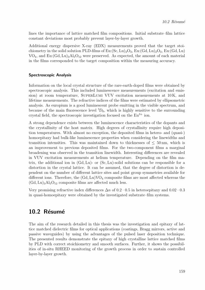
10.2 Resume
lines the importance of lattice matched film compositions. Initial substrate–film latticeconstant deviations most probably prevent layer-by-layer growth.
Additional energy dispersive X-ray (EDX) measurements proved that the target stoi-chiometry in the solid solution PLD-films of Eu:(Sc, Lu)2O3, Eu:(Gd, Lu)2O3, Eu:(Gd, Lu)VO4, and Eu:(Gd, Lu)3Al5O12 were preserved. As expected, the amount of each materialin the films corresponded to the target composition within the measuring accuracy.
Spectroscopic Analysis
Information on the local crystal structure of the rare-earth-doped films were obtained byspectroscopic analysis. This included luminescence measurements (excitation and emis-sion) at room temperature, SuperLumi VUV excitation measurements at 10K, andlifetime measurements. The refractive indices of the films were estimated by ellipsometricanalysis. As europium is a good luminescent probe emitting in the visible spectrum, andbecause of the main fluorescence level 5D0, which is highly sensitive to the surroundingcrystal field, the spectroscopic investigation focused on the Eu3+ ion.
A strong dependence exists between the luminescence characteristics of the dopants andthe crystallinity of the host matrix. High degrees of crystallinity require high deposi-tion temperatures. With almost no exception, the deposited films in hetero- and (quasi-)homoepitaxy had bulk-like luminescence properties when considering the linewidths andtransition intensities. This was maintained down to thicknesses of ≤ 50 nm, which isan improvement to previous deposited films. For the two-component films a marginalbroadening was observed in the transition linewidth. Interesting differences are revealedin VUV excitation measurements at helium temperature. Depending on the film ma-trix, the additional ion in (Gd, Lu)- or (Sc, Lu)-solid solutions can be responsible for adistortion in the crystal lattice. It can be assumed, that the degree of distortion is de-pendent on the number of different lattice sites and point group symmetries available fordifferent ions. Therefore, the (Gd, Lu)VO4 composite films are most affected whereas the(Gd, Lu)3Al5O12 composite films are affected much less.
Very promising refractive index differences ∆n of 0.2 – 0.5 in heteroepitaxy and 0.02 – 0.3in quasi-homoepitaxy were obtained by the investigated substrate–film systems.
10.2 Resume
The aim of the research detailed in this thesis was the investigation and epitaxy of lat-tice matched dielectric films for optical applications (coatings, Bragg mirrors, active andpassive waveguides) by using the advantages of the pulsed laser deposition technique.The presented results demonstrate the epitaxy of high crystalline lattice matched filmsby PLD with correct stoichiometry and smooth surfaces. Further, it shows the possibil-ities of in-situ RHEED monitoring of the growth process in order to sustain controlledlayer-by-layer growth.
159
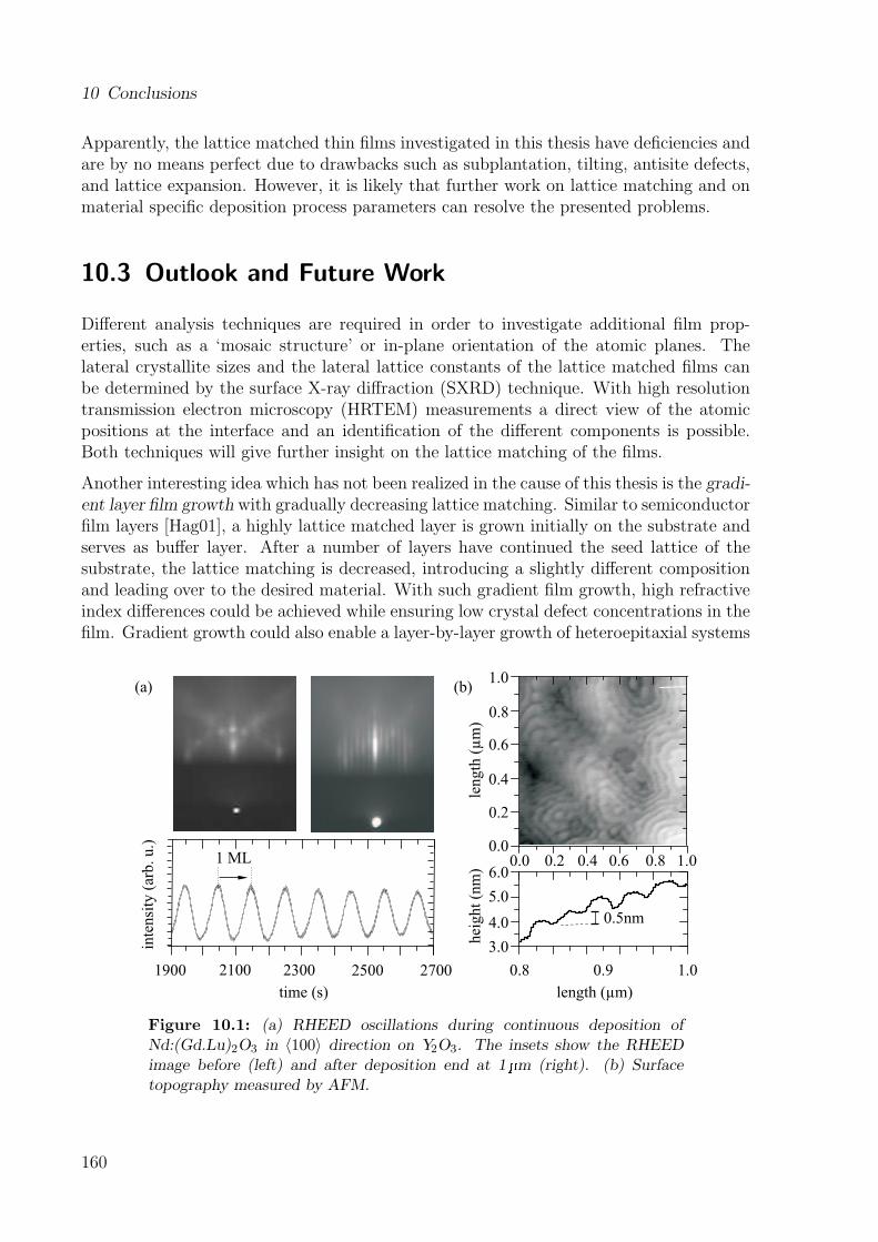
10 Conclusions
Apparently, the lattice matched thin films investigated in this thesis have deficiencies andare by no means perfect due to drawbacks such as subplantation, tilting, antisite defects,and lattice expansion. However, it is likely that further work on lattice matching and onmaterial specific deposition process parameters can resolve the presented problems.
10.3 Outlook and Future Work
Different analysis techniques are required in order to investigate additional film prop-erties, such as a ‘mosaic structure’ or in-plane orientation of the atomic planes. Thelateral crystallite sizes and the lateral lattice constants of the lattice matched films canbe determined by the surface X-ray diffraction (SXRD) technique. With high resolutiontransmission electron microscopy (HRTEM) measurements a direct view of the atomicpositions at the interface and an identification of the different components is possible.Both techniques will give further insight on the lattice matching of the films.
Another interesting idea which has not been realized in the cause of this thesis is the gradi-ent layer film growth with gradually decreasing lattice matching. Similar to semiconductorfilm layers [Hag01], a highly lattice matched layer is grown initially on the substrate andserves as buffer layer. After a number of layers have continued the seed lattice of thesubstrate, the lattice matching is decreased, introducing a slightly different compositionand leading over to the desired material. With such gradient film growth, high refractiveindex differences could be achieved while ensuring low crystal defect concentrations in thefilm. Gradient growth could also enable a layer-by-layer growth of heteroepitaxial systems
inte
nsi
ty (
arb
. u
.)
1900 2100 2300 2500
time (s)
2700
(a) (b)
0.8 0.9 1.0
length ( m)µ
length
(m
)µ
hei
ght
(nm
)
0.0
0.2
0.4
0.6
0.8
1.0
3.0
4.0
5.0
6.01 ML 0.0 0.2 0.4 0.6 0.8 1.0
0.5nm
Figure 10.1: (a) RHEED oscillations during continuous deposition ofNd:(Gd.Lu)2O3 in 〈100〉 direction on Y2O3. The insets show the RHEEDimage before (left) and after deposition end at 1 � m (right). (b) Surfacetopography measured by AFM.
160
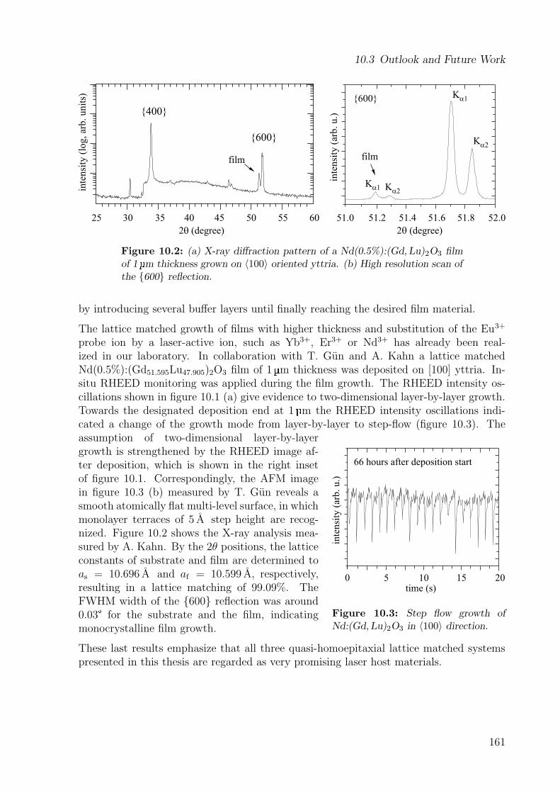
10.3 Outlook and Future Work
inte
nsi
ty (
log
, ar
b.
un
its)
{400}
{600}
inte
nsi
ty (
arb
. u
.)
{600}
Ka2
Ka1
film
Ka2
Ka1
25 30 35 40 45 55 6050
2 (degree)q
51.0 51.2 51.4
2q (degree)
52.051.6 51.8
film
Figure 10.2: (a) X-ray diffraction pattern of a Nd(0.5%):(Gd, Lu)2O3 filmof 1 � m thickness grown on 〈100〉 oriented yttria. (b) High resolution scan ofthe {600} reflection.
by introducing several buffer layers until finally reaching the desired film material.
The lattice matched growth of films with higher thickness and substitution of the Eu3+
probe ion by a laser-active ion, such as Yb3+, Er3+ or Nd3+ has already been real-ized in our laboratory. In collaboration with T. Gun and A. Kahn a lattice matchedNd(0.5%):(Gd51.595Lu47.905)2O3 film of 1 � m thickness was deposited on [100] yttria. In-situ RHEED monitoring was applied during the film growth. The RHEED intensity os-cillations shown in figure 10.1 (a) give evidence to two-dimensional layer-by-layer growth.Towards the designated deposition end at 1 � m the RHEED intensity oscillations indi-cated a change of the growth mode from layer-by-layer to step-flow (figure 10.3). The
inte
nsi
ty (
arb
. u
.)
0 5 10 15time (s)
20
66 hours after deposition start
Figure 10.3: Step flow growth ofNd:(Gd, Lu)2O3 in 〈100〉 direction.
assumption of two-dimensional layer-by-layergrowth is strengthened by the RHEED image af-ter deposition, which is shown in the right insetof figure 10.1. Correspondingly, the AFM imagein figure 10.3 (b) measured by T. Gun reveals asmooth atomically flat multi-level surface, in whichmonolayer terraces of 5 A step height are recog-nized. Figure 10.2 shows the X-ray analysis mea-sured by A. Kahn. By the 2θ positions, the latticeconstants of substrate and film are determined toas = 10.696 A and af = 10.599 A, respectively,resulting in a lattice matching of 99.09%. TheFWHM width of the {600} reflection was around0.03 � for the substrate and the film, indicatingmonocrystalline film growth.
These last results emphasize that all three quasi-homoepitaxial lattice matched systemspresented in this thesis are regarded as very promising laser host materials.
161

10 Conclusions
162
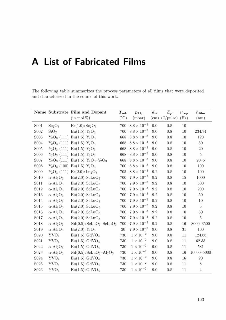
A List of Fabricated Films
The following table summarizes the process parameters of all films that were depositedand characterized in the course of this work.
Name Substrate Film and Dopant Tsub pO2dts Ep νrep hfilm
(in mol.%) ( � C) (mbar) (cm) (J/pulse) (Hz) (nm)
S001 Sc2O3 Er(1.0): Sc2O3 700 8.8× 10⁻³ 9.0 0.8 10
S002 SiO2 Eu(1.5): Y2O3 700 8.8× 10⁻³ 9.0 0.8 10 234.74
S003 Y2O3 (111) Eu(1.5): Y2O3 668 8.8× 10⁻³ 9.0 0.8 10 120
S004 Y2O3 (111) Eu(1.5): Y2O3 668 8.8× 10⁻³ 9.0 0.8 10 50
S005 Y2O3 (111) Eu(1.5): Y2O3 668 8.8× 10⁻³ 9.0 0.8 10 20
S006 Y2O3 (111) Eu(1.5): Y2O3 668 8.8× 10⁻³ 9.0 0.8 10 5
S007 Y2O3 (111) Eu(1.5): Y2O3–Y2O3 668 8.8× 10⁻³ 9.0 0.8 10 20–5
S008 Y2O3 (100) Eu(1.5): Y2O3 700 8.8× 10⁻³ 9.0 0.8 10 100
S009 Y2O3 (111) Er(2.0): Lu2O3 705 8.8× 10⁻³ 9.2 0.8 10 100
S010 α-Al2O3 Eu(2.0): ScLuO3 700 7.9× 10⁻³ 9.2 0.8 15 1000
S011 α-Al2O3 Eu(2.0): ScLuO3 700 7.9× 10⁻³ 9.2 0.8 10 500
S012 α-Al2O3 Eu(2.0): ScLuO3 700 7.9× 10⁻³ 9.2 0.8 10 200
S013 α-Al2O3 Eu(2.0): ScLuO3 700 7.9× 10⁻³ 9.2 0.8 10 50
S014 α-Al2O3 Eu(2.0): ScLuO3 700 7.9× 10⁻³ 9.2 0.8 10 10
S015 α-Al2O3 Eu(2.0): ScLuO3 700 7.9× 10⁻³ 9.2 0.8 10 5
S016 α-Al2O3 Eu(2.0): ScLuO3 700 7.9× 10⁻³ 9.2 0.8 10 50
S017 α-Al2O3 Eu(2.0): ScLuO3 700 7.9× 10⁻³ 9.2 0.8 10 5
S018 α-Al2O3 Nd(0.5): ScLuO3–ScLuO3 700 7.9× 10⁻³ 9.2 0.8 16 8000–3500
S019 α-Al2O3 Eu(2.0): Y2O3 20 7.9× 10⁻³ 9.0 0.8 31 100
S020 YVO4 Eu(1.5):GdVO4 730 1× 10⁻² 9.0 0.8 11 124.66
S021 YVO4 Eu(1.5):GdVO4 730 1× 10⁻² 9.0 0.8 11 62.33
S022 α-Al2O3 Eu(1.5):GdVO4 730 1× 10⁻² 9.0 0.8 11 581
S023 α-Al2O3 Nd(0.5): ScLuO3–Al2O3 730 1× 10⁻² 9.0 0.8 16 10000–5000
S024 YVO4 Eu(1.5):GdVO4 730 1× 10⁻² 9.0 0.8 16 20
S025 YVO4 Eu(1.5):GdVO4 730 1× 10⁻² 9.0 0.8 11 8
S026 YVO4 Eu(1.5):GdVO4 730 1× 10⁻² 9.0 0.8 11 4
163
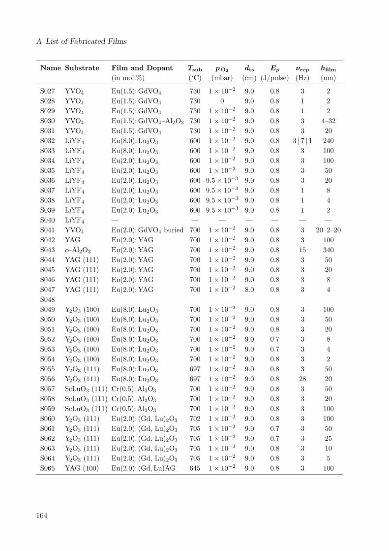
A List of Fabricated Films
Name Substrate Film and Dopant Tsub pO2dts Ep νrep hfilm
(in mol.%) ( � C) (mbar) (cm) (J/pulse) (Hz) (nm)
S027 YVO4 Eu(1.5):GdVO4 730 1× 10⁻² 9.0 0.8 3 2
S028 YVO4 Eu(1.5):GdVO4 730 0 9.0 0.8 1 2
S029 YVO4 Eu(1.5):GdVO4 730 1× 10⁻² 9.0 0.8 1 2
S030 YVO4 Eu(1.5):GdVO4–Al2O3 730 1× 10⁻² 9.0 0.8 3 4–32
S031 YVO4 Eu(1.5):GdVO4 730 1× 10⁻² 9.0 0.8 3 20
S032 LiYF4 Eu(8.0): Lu2O3 600 1× 10⁻² 9.0 0.8 3 | 7 | 1 240
S033 LiYF4 Eu(8.0): Lu2O3 600 1× 10⁻² 9.0 0.8 3 100
S034 LiYF4 Eu(2.0): Lu2O3 600 1× 10⁻² 9.0 0.8 3 100
S035 LiYF4 Eu(2.0): Lu2O3 600 1× 10⁻² 9.0 0.8 3 50
S036 LiYF4 Eu(2.0): Lu2O3 600 9.5× 10⁻³ 9.0 0.8 3 20
S037 LiYF4 Eu(2.0): Lu2O3 600 9.5× 10⁻³ 9.0 0.8 1 8
S038 LiYF4 Eu(2.0): Lu2O3 600 9.5× 10⁻³ 9.0 0.8 1 4
S039 LiYF4 Eu(2.0): Lu2O3 600 9.5× 10⁻³ 9.0 0.8 1 2
S040 LiYF4 — — — — — — —
S041 YVO4 Eu(2.0):GdVO4 buried 700 1× 10⁻² 9.0 0.8 3 20–2–20
S042 YAG Eu(2.0): YAG 700 1× 10⁻² 9.0 0.8 3 100
S043 α-Al2O3 Eu(2.0): YAG 700 1× 10⁻² 9.0 0.8 15 340
S044 YAG (111) Eu(2.0): YAG 700 1× 10⁻² 9.0 0.8 3 50
S045 YAG (111) Eu(2.0): YAG 700 1× 10⁻² 9.0 0.8 3 20
S046 YAG (111) Eu(2.0): YAG 700 1× 10⁻² 9.0 0.8 3 8
S047 YAG (111) Eu(2.0): YAG 700 1× 10⁻² 8.0 0.8 3 4
S048
S049 Y2O3 (100) Eu(8.0): Lu2O3 700 1× 10⁻² 9.0 0.8 3 100
S050 Y2O3 (100) Eu(8.0): Lu2O3 700 1× 10⁻² 9.0 0.8 3 50
S051 Y2O3 (100) Eu(8.0): Lu2O3 700 1× 10⁻² 9.0 0.8 3 20
S052 Y2O3 (100) Eu(8.0): Lu2O3 700 1× 10⁻² 9.0 0.7 3 8
S053 Y2O3 (100) Eu(8.0): Lu2O3 700 1× 10⁻² 9.0 0.7 3 4
S054 Y2O3 (100) Eu(8.0): Lu2O3 700 1× 10⁻² 9.0 0.8 3 2
S055 Y2O3 (111) Eu(8.0): Lu2O3 697 1× 10⁻² 9.0 0.8 3 50
S056 Y2O3 (111) Eu(8.0): Lu2O3 697 1× 10⁻² 9.0 0.8 28 20
S057 ScLuO3 (111) Cr(0.5): Al2O3 700 1× 10⁻² 9.0 0.8 3 50
S058 ScLuO3 (111) Cr(0.5): Al2O3 700 1× 10⁻² 9.0 0.8 3 20
S059 ScLuO3 (111) Cr(0.5): Al2O3 700 1× 10⁻² 9.0 0.8 3 100
S060 Y2O3 (111) Eu(2.0): (Gd, Lu)2O3 702 1× 10⁻² 9.0 0.8 3 100
S061 Y2O3 (111) Eu(2.0): (Gd, Lu)2O3 705 1× 10⁻² 9.0 0.7 3 50
S062 Y2O3 (111) Eu(2.0): (Gd, Lu)2O3 705 1× 10⁻² 9.0 0.7 3 25
S063 Y2O3 (111) Eu(2.0): (Gd, Lu)2O3 705 1× 10⁻² 9.0 0.8 3 10
S064 Y2O3 (111) Eu(2.0): (Gd, Lu)2O3 705 1× 10⁻² 9.0 0.8 3 5
S065 YAG (100) Eu(2.0): (Gd, Lu)AG 645 1× 10⁻² 9.0 0.8 3 100
164
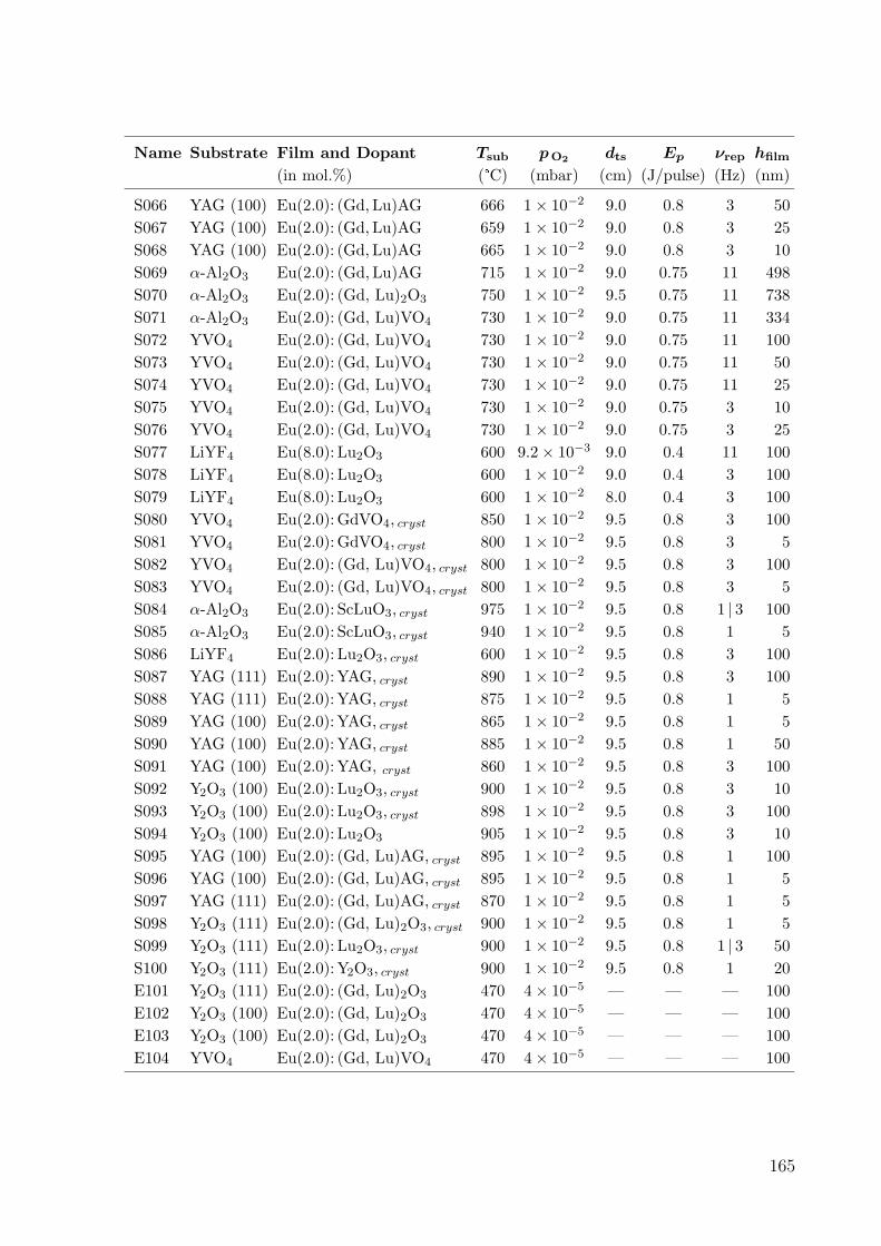
Name Substrate Film and Dopant Tsub pO2dts Ep νrep hfilm
(in mol.%) ( � C) (mbar) (cm) (J/pulse) (Hz) (nm)
S066 YAG (100) Eu(2.0): (Gd, Lu)AG 666 1× 10⁻² 9.0 0.8 3 50
S067 YAG (100) Eu(2.0): (Gd, Lu)AG 659 1× 10⁻² 9.0 0.8 3 25
S068 YAG (100) Eu(2.0): (Gd, Lu)AG 665 1× 10⁻² 9.0 0.8 3 10
S069 α-Al2O3 Eu(2.0): (Gd, Lu)AG 715 1× 10⁻² 9.0 0.75 11 498
S070 α-Al2O3 Eu(2.0): (Gd, Lu)2O3 750 1× 10⁻² 9.5 0.75 11 738
S071 α-Al2O3 Eu(2.0): (Gd, Lu)VO4 730 1× 10⁻² 9.0 0.75 11 334
S072 YVO4 Eu(2.0): (Gd, Lu)VO4 730 1× 10⁻² 9.0 0.75 11 100
S073 YVO4 Eu(2.0): (Gd, Lu)VO4 730 1× 10⁻² 9.0 0.75 11 50
S074 YVO4 Eu(2.0): (Gd, Lu)VO4 730 1× 10⁻² 9.0 0.75 11 25
S075 YVO4 Eu(2.0): (Gd, Lu)VO4 730 1× 10⁻² 9.0 0.75 3 10
S076 YVO4 Eu(2.0): (Gd, Lu)VO4 730 1× 10⁻² 9.0 0.75 3 25
S077 LiYF4 Eu(8.0): Lu2O3 600 9.2× 10⁻³ 9.0 0.4 11 100
S078 LiYF4 Eu(8.0): Lu2O3 600 1× 10⁻² 9.0 0.4 3 100
S079 LiYF4 Eu(8.0): Lu2O3 600 1× 10⁻² 8.0 0.4 3 100
S080 YVO4 Eu(2.0):GdVO4, cryst 850 1× 10⁻² 9.5 0.8 3 100
S081 YVO4 Eu(2.0):GdVO4, cryst 800 1× 10⁻² 9.5 0.8 3 5
S082 YVO4 Eu(2.0): (Gd, Lu)VO4, cryst 800 1× 10⁻² 9.5 0.8 3 100
S083 YVO4 Eu(2.0): (Gd, Lu)VO4, cryst 800 1× 10⁻² 9.5 0.8 3 5
S084 α-Al2O3 Eu(2.0): ScLuO3, cryst 975 1× 10⁻² 9.5 0.8 1 | 3 100
S085 α-Al2O3 Eu(2.0): ScLuO3, cryst 940 1× 10⁻² 9.5 0.8 1 5
S086 LiYF4 Eu(2.0): Lu2O3, cryst 600 1× 10⁻² 9.5 0.8 3 100
S087 YAG (111) Eu(2.0): YAG, cryst 890 1× 10⁻² 9.5 0.8 3 100
S088 YAG (111) Eu(2.0): YAG, cryst 875 1× 10⁻² 9.5 0.8 1 5
S089 YAG (100) Eu(2.0): YAG, cryst 865 1× 10⁻² 9.5 0.8 1 5
S090 YAG (100) Eu(2.0): YAG, cryst 885 1× 10⁻² 9.5 0.8 1 50
S091 YAG (100) Eu(2.0): YAG, cryst 860 1× 10⁻² 9.5 0.8 3 100
S092 Y2O3 (100) Eu(2.0): Lu2O3, cryst 900 1× 10⁻² 9.5 0.8 3 10
S093 Y2O3 (100) Eu(2.0): Lu2O3, cryst 898 1× 10⁻² 9.5 0.8 3 100
S094 Y2O3 (100) Eu(2.0): Lu2O3 905 1× 10⁻² 9.5 0.8 3 10
S095 YAG (100) Eu(2.0): (Gd, Lu)AG, cryst 895 1× 10⁻² 9.5 0.8 1 100
S096 YAG (100) Eu(2.0): (Gd, Lu)AG, cryst 895 1× 10⁻² 9.5 0.8 1 5
S097 YAG (111) Eu(2.0): (Gd, Lu)AG, cryst 870 1× 10⁻² 9.5 0.8 1 5
S098 Y2O3 (111) Eu(2.0): (Gd, Lu)2O3, cryst 900 1× 10⁻² 9.5 0.8 1 5
S099 Y2O3 (111) Eu(2.0): Lu2O3, cryst 900 1× 10⁻² 9.5 0.8 1 | 3 50
S100 Y2O3 (111) Eu(2.0): Y2O3, cryst 900 1× 10⁻² 9.5 0.8 1 20
E101 Y2O3 (111) Eu(2.0): (Gd, Lu)2O3 470 4× 10⁻⁵ — — — 100
E102 Y2O3 (100) Eu(2.0): (Gd, Lu)2O3 470 4× 10⁻⁵ — — — 100
E103 Y2O3 (100) Eu(2.0): (Gd, Lu)2O3 470 4× 10⁻⁵ — — — 100
E104 YVO4 Eu(2.0): (Gd, Lu)VO4 470 4× 10⁻⁵ — — — 100
165
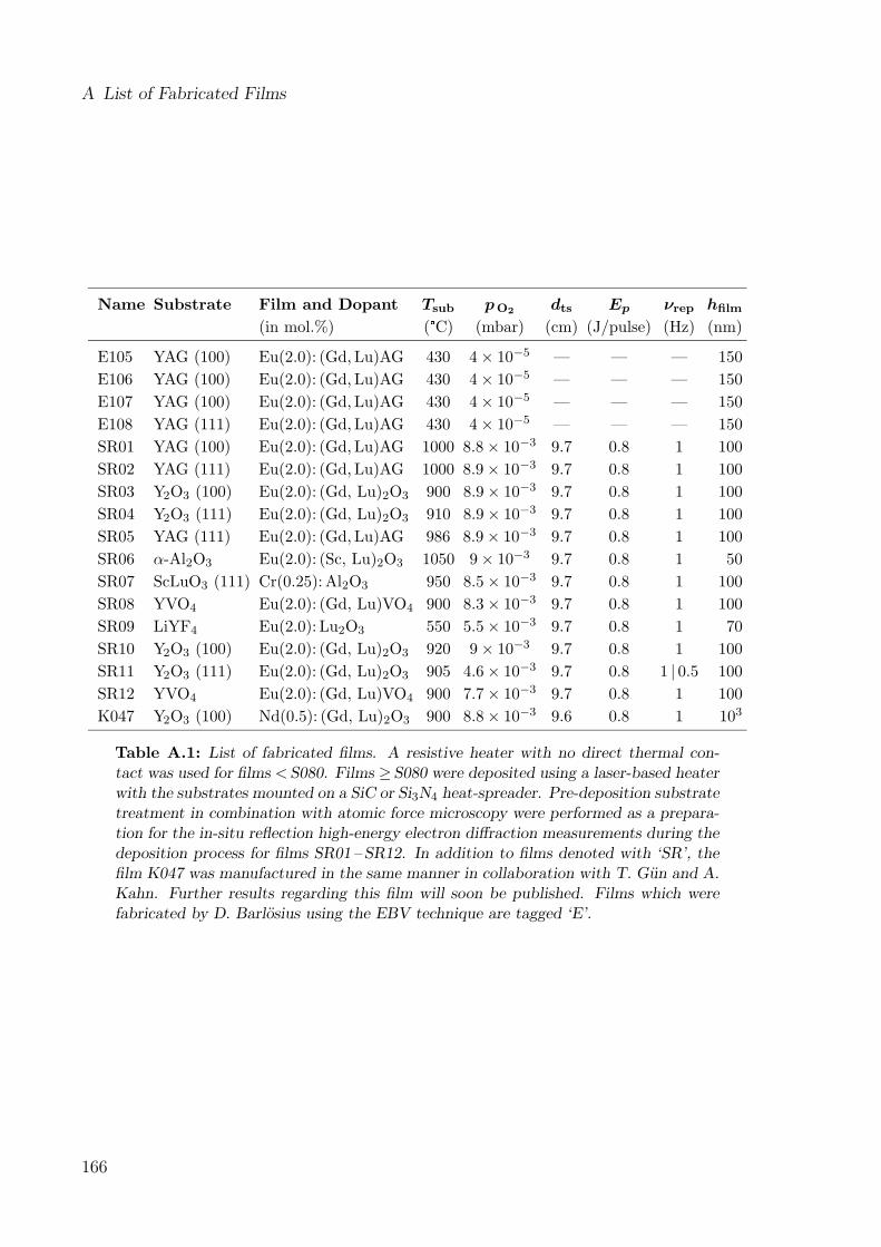
A List of Fabricated Films
Name Substrate Film and Dopant Tsub pO2dts Ep νrep hfilm
(in mol.%) ( � C) (mbar) (cm) (J/pulse) (Hz) (nm)
E105 YAG (100) Eu(2.0): (Gd, Lu)AG 430 4× 10⁻⁵ — — — 150
E106 YAG (100) Eu(2.0): (Gd, Lu)AG 430 4× 10⁻⁵ — — — 150
E107 YAG (100) Eu(2.0): (Gd, Lu)AG 430 4× 10⁻⁵ — — — 150
E108 YAG (111) Eu(2.0): (Gd, Lu)AG 430 4× 10⁻⁵ — — — 150
SR01 YAG (100) Eu(2.0): (Gd, Lu)AG 1000 8.8× 10⁻³ 9.7 0.8 1 100
SR02 YAG (111) Eu(2.0): (Gd, Lu)AG 1000 8.9× 10⁻³ 9.7 0.8 1 100
SR03 Y2O3 (100) Eu(2.0): (Gd, Lu)2O3 900 8.9× 10⁻³ 9.7 0.8 1 100
SR04 Y2O3 (111) Eu(2.0): (Gd, Lu)2O3 910 8.9× 10⁻³ 9.7 0.8 1 100
SR05 YAG (111) Eu(2.0): (Gd, Lu)AG 986 8.9× 10⁻³ 9.7 0.8 1 100
SR06 α-Al2O3 Eu(2.0): (Sc, Lu)2O3 1050 9× 10⁻³ 9.7 0.8 1 50
SR07 ScLuO3 (111) Cr(0.25): Al2O3 950 8.5× 10⁻³ 9.7 0.8 1 100
SR08 YVO4 Eu(2.0): (Gd, Lu)VO4 900 8.3× 10⁻³ 9.7 0.8 1 100
SR09 LiYF4 Eu(2.0): Lu2O3 550 5.5× 10⁻³ 9.7 0.8 1 70
SR10 Y2O3 (100) Eu(2.0): (Gd, Lu)2O3 920 9× 10⁻³ 9.7 0.8 1 100
SR11 Y2O3 (111) Eu(2.0): (Gd, Lu)2O3 905 4.6× 10⁻³ 9.7 0.8 1 | 0.5 100
SR12 YVO4 Eu(2.0): (Gd, Lu)VO4 900 7.7× 10⁻³ 9.7 0.8 1 100
K047 Y2O3 (100) Nd(0.5): (Gd, Lu)2O3 900 8.8× 10⁻³ 9.6 0.8 1 103
Table A.1: List of fabricated films. A resistive heater with no direct thermal con-tact was used for films <S080. Films ≥ S080 were deposited using a laser-based heaterwith the substrates mounted on a SiC or Si3N4 heat-spreader. Pre-deposition substratetreatment in combination with atomic force microscopy were performed as a prepara-tion for the in-situ reflection high-energy electron diffraction measurements during thedeposition process for films SR01 – SR12. In addition to films denoted with ‘SR’, thefilm K047 was manufactured in the same manner in collaboration with T. Gun and A.Kahn. Further results regarding this film will soon be published. Films which werefabricated by D. Barlosius using the EBV technique are tagged ‘E’.
166
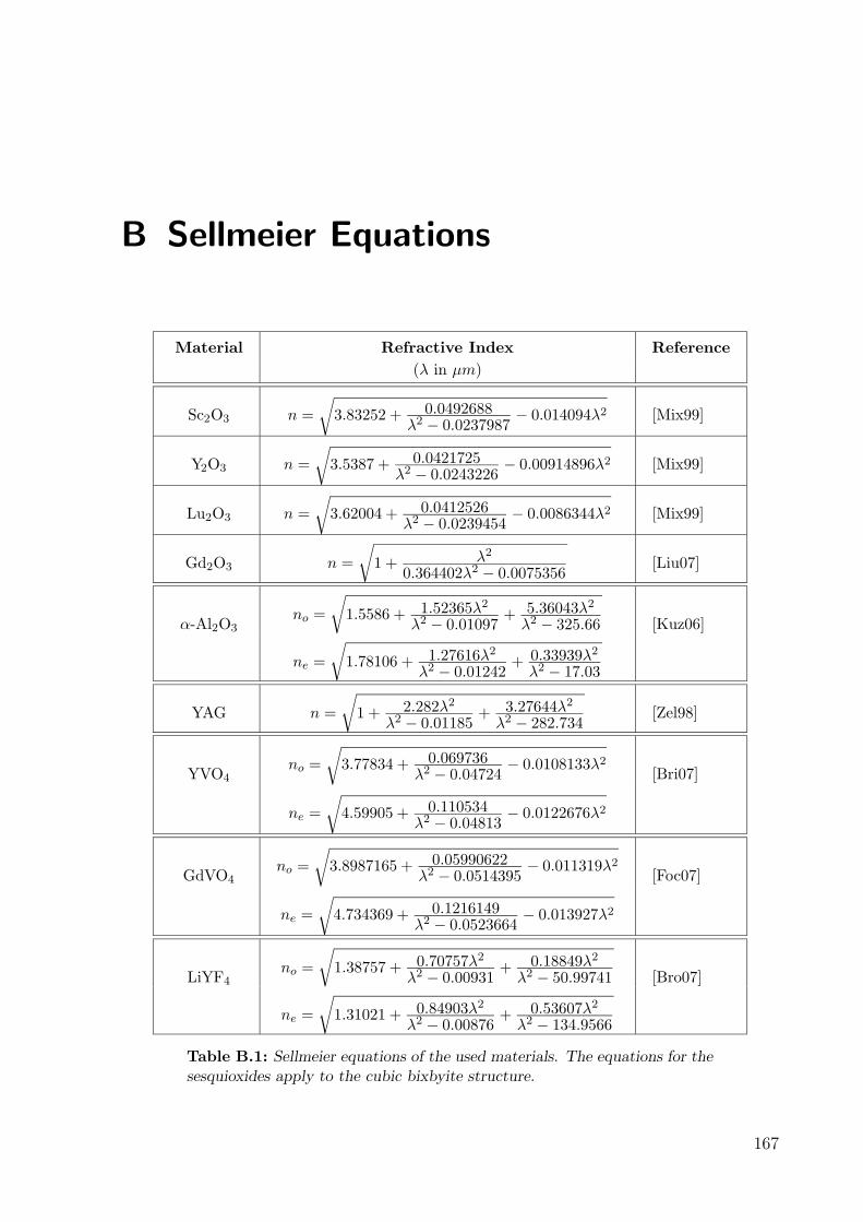
B Sellmeier Equations
Material Refractive Index Reference
(λ in µm)
Sc2O3 n =
√
3.83252 + 0.0492688λ2 − 0.0237987 − 0.014094λ
2 [Mix99]
Y2O3 n =
√
3.5387 + 0.0421725λ2 − 0.0243226 − 0.00914896λ
2 [Mix99]
Lu2O3 n =
√
3.62004 + 0.0412526λ2 − 0.0239454 − 0.0086344λ
2 [Mix99]
Gd2O3 n =
√
1 + λ2
0.364402λ2 − 0.0075356 [Liu07]
α-Al2O3no =
√
1.5586 + 1.52365λ2
λ2 − 0.01097 +5.36043λ2
λ2 − 325.66 [Kuz06]
ne =
√
1.78106 + 1.27616λ2
λ2 − 0.01242 +0.33939λ2
λ2 − 17.03
YAG n =
√
1 + 2.282λ2
λ2 − 0.01185 +3.27644λ2
λ2 − 282.734 [Zel98]
YVO4no =
√
3.77834 + 0.069736λ2 − 0.04724 − 0.0108133λ
2[Bri07]
ne =
√
4.59905 + 0.110534λ2 − 0.04813 − 0.0122676λ
2
GdVO4no =
√
3.8987165 + 0.05990622λ2 − 0.0514395 − 0.011319λ
2[Foc07]
ne =
√
4.734369 + 0.1216149λ2 − 0.0523664 − 0.013927λ
2
LiYF4no =
√
1.38757 + 0.70757λ2
λ2 − 0.00931 +0.18849λ2
λ2 − 50.99741 [Bro07]
ne =
√
1.31021 + 0.84903λ2
λ2 − 0.00876 +0.53607λ2
λ2 − 134.9566
Table B.1: Sellmeier equations of the used materials. The equations for thesesquioxides apply to the cubic bixbyite structure.
167

B Sellmeier Equations
168
Bibliography
[Abr78] V. N. Abramov and A. I. Kuznetsnov, Fundamental absorption of Y2O3
and YAlO3 , Soviet Physics of Solid State 20 (3), 399 (1978).
[Abr83] V. N. Abramov, A. N. Ermoshkin and A. I. Kuznetsnov, Optical prop-erties and electron energy structure of Y2O3 and Sc2O3 , Soviet Physics of SolidState 25 (6), 981 (1983).
[And94] F. Anderson, P. Summers, H. Weidner, P. Hong and R. Peale, In-terpretive crystal-field parameters: Application to Nd3+ in GdVO4 and YVO4,Physical Review B 50 (20) (1994).
[And96] S. Andrieu and P. Frechard, What information can be obtained by RHEEDapplied on polycrystalline films? , Surface Science 360 (1), 289 (1996).
[And98] A. A. Anderson, Crystalline planar waveguide lasers fabricated by pulsed laserdeposition, Dissertation, Faculty of Science, Department of Physics, Universityof Southampton (1998).
[Ani83] S. I. Anisimov, Y. B. Zel’dovich, N. A. Inogamov and M. F. Ivanov,Shock Waves, Explosions, and Detonations , in: Progress in Astronautics andAeronautics, Series 87 , 218 (Washington, DC, 1983).
[Ash76] N. W. Ashcroft and N. D. Mermin, Solid State Physics (Saunders CollegePublishing, Fort Worth, 1976).
[Atk87] P. W. Atkins, Physikalische Chemie (VCH Verlag, 1987).
[Auc88] O. Auciello, A. R. Krauss, J. Santiago-Aviles, A. F. Schreiner andD. M. Gruen, Surface compositional and topographical changes resulting fromexcimer laser impacting on YBa2Cu3O2 single phase superconductors , AppliedPhysics Letters 52 (3), 239 (1988).
[Bab05] V. Babin, K. Blazek, A. Krasnikov, K. Nejezchleb, M. Nikl,T. Savikhina and S. Zazubovich, Luminescence of undoped LuAG and YAGcrystals , Physica Status Solidi C 2 (1), 97 (2005).
[Bal62] C. J. Ballhausen, Introduction to Ligand Field Theory (McGraw-Hill BookCompany, Inc., New York, 1962).
169
Bibliography
[Bal67] R. Balzer, H. Peisl and W. Waidelich, Gitterfehlordnung in KCL mitFarbzentren, Zeitschrift fur Physik 204, 405 (1967).
[Bar57] C. Barta, F. Petru and B. Hajek, Uber die Darstellung des Einkristallsvon Scandiumoxyd , Die Naturwissenschaften 45, 36 (1957).
[Bar69] W. P. Barr, The production of low scattering dielectric mirrors using rotatingvane particle filtration, Journal of Physics E 2 (2), 1112 (1969).
[Bar74] B. D. Bartolo, Optical properties of ions in solids (Plenum Press, New York,1974).
[Bar95] A.-L. Barabasi and H. E. Stanley, Fractal concepts in surface growth(Cambridge University Press, 1995).
[Bar01] S. J. Barrington, Planar Waveguide Devices fabricated by Pulsed Laser De-position, Dissertation, Faculty of Science, Department of Physics, University ofSouthampton (2001).
[Bar04] S. Bar, Crystalline, Rare-Earth-doped Sesquioxide PLD-Films on α-Alumina,Dissertation, Fachbereich Physik, Universitat Hamburg (2004).
[Bar05] S. Bar, H. Scheife and G. Huber, Rare-earth-doped GVO films grown bypulsed laser deposition, Optical Materials 28 (6-7), 681 (2005).
[Bas95] M. Bass, Handbook of optics (McGraw-Hill Book Company, Inc., New York,1995), 2nd edition.
[Bat82] I. P. Batra, Electronic structure of α-Al2O3 , Journal of Physics: CondensedMatter 15, 5399 (1982).
[Bau58] E. Bauer, Wachstum dunner Schichten, Zeitschrift fur Kristallographie 110,372 (1958).
[Bau00] D. Bauerle, Laser Processing and Chemistry (Springer-Verlag, Berlin, Hei-delberg, New York, 2000).
[Bec88] C. H. Becker and J. Pallix, Laser ablation of bulk YBa2Cu3O7−δ andcluster emission, Journal of Applied Physics 64 (10), 5152 (1988).
[Bee88] J. L. Beeby, in: P. K. Larsen and P. J. Dobson (editors), Reflection High-Energy Electron Diffraction and Reflection Electron Imaging (Plenum, New Yorkand London, 1988).
[Bel03] E. L. Belokoneva and Y. K. Shcherbakova, Electron density in syntheticescolaite Cr2O3 with a corundum structure and its relation to antiferromagneticproperties , Zhurnal Neorganicheskoi Khimii 48, 960 (2003).
[Ber66] L. Bergmann and C. Schafer, Lehrbuch der Experimentalphysik, AusgabeIII (Walter de Gruyter & Co, 1966).
170
Bibliography
[Ber74] H. Bergmann, Gmelin Handbuch der Anorganischen Chemie, Seltenerdele-mente, Teil C1 (Springer-Verlag, Berlin, Heidelberg, New York, 1974).
[Bin86] G. Binning, C. Quate and C. Gerber, Atomic Force Microscope, PhysicalReview Letters 56 (9), 930 (1986).
[Blo74] N. Bloembergen, Laser-Induced Electric Breakdown in Solids , IEEE Journalof Quantum Electronics QE-10 (3), 375 (1974).
[Bol88] B. Bolger, P. K. Larsen and G. Meyer-Ehmsen, in: P. K. Larsenand P. J. Dobson (editors), Reflection High-Energy Electron Diffraction andReflection Electron Imaging (Plenum, New York and London, 1988).
[Bon00] C. L. Bonner,Multi-watt, diode-pumped planar waveguide lasers , Dissertation,Faculty of Science, Department of Physics, University Southampton (2000).
[Bor27] M. Born and J. R. Oppenheimer, Zur Quantentheorie der Molekule, An-nalen der Physik 84, 457 (1927).
[Bor75] M. Born and E. Wolf, Principles of Optics, 5th edition (Pergamon Press,Oxford, 1975).
[Bra92] S. Brandt, Datenanalyse, 3. Auflage (BI Wissenschaftsverlag, Mannheim,1992).
[Bra99] W. Braun, Applied RHEED (Spinger Tracts in Modern Physics, Springer-Verlag, Berlin, Heidelberg, New York, 1999).
[Bre62] F. Breech and L. Cross, Applied Spectroscopy 16 (1962).
[Bri07] I. Brightcrystal, http://www.brightcrystals.com/english/readnew.asp?NewsID=4914(2007).
[Bro95] I. N. Bronstein, K. A. Sememdjajew, G. Musiol and H. Muhling,Taschenbuch der Mathematik (Verlag Harry Deutsch, Frankfurt amMain, 1995).
[Bro07] I. Broadband, http://www.bblaser.com/bbl item/0156aotk ndylf.html(2007).
[Bul95] A. V. Bulgakov and N. M. Bulgakova, Dynamics of laser-induced plumeexpansion into an ambient gas during film deposition, Journal of Physics D:Applied Physics 28 (8), 1710 (1995).
[Bul98] A. V. Bulgakov and N. M. Bulgakova, Gas-dynamic effects of the inter-action between a pulsed laser-ablation plume and the ambient gas: analogy withan underepanded jet , Journal of Physics D 31, 693 (1998).
[Bun89] J.-C. G. Bunzli and G. R. Choppin, Lanthanide Probes in Life, Chemi-cal and Earth Sciences (Elsevier Science Publishing Company Inc., New York,1989).
171
Bibliography
[Bur62] G. Burns, Shielding and Crystal Fields at Rare-Earth Ions , Physical Review128 (5), 2121 (1962).
[Bur02] P. Burmester, Optisch aktive, kristalline, Selten-Erd-dotierte Y2O3 -PLD-Schichten auf α-Al2O3 , Dissertation, Fachbereich Physik, Universitat Hamburg(2002).
[Che88] J. T. Cheung and H. Sankur, Growth of thin films by laser-induced evap-oration, CRC Critical Reviews in Solid State and Material Sciences 14 (1), 63(1988).
[Che01] R. Chety, E. Millon, A. Boudrioua, J. C. Loulergue, A. Dahounand J. Perriere, Growth of GdCa4O(BO3 )3 thin films by pulsed-laser deposi-tion for nonlinear optical applications , Journal of Materials Chemistry 11, 657(2001).
[Che04] T. Chen, X. M. Li, S. Zhang and H. R. Zeng, Oxygen dependence of thecrystallinity of MgO films grown on Si(100) by PLD , Journal of Crystal Growth270, 553 (2004).
[Chi99] W. Y. Ching and Y.-N. Xu, Nonscalability and nontransferability in theelectronic properties of the Y-Al-O system, Phys. Rev. B 59, 12815 (1999).
[Cho99] M. H. Cho, D. H. Ko, K. Jeong, I. W. Lyo, S. W. Whangbo, H. B.Kim, S. Choi, J. H. Song, S. Cho and C. N. Whang, Temperature depen-dence of the properties of heteroepitaxial Y2O3 films grown on Si by ion assistedevaporation, Journal of Applied Physics 86 (1), 198 (1999).
[Chr94] D. B. Chrisey and G. K. Hubler, Pulsed laser deposition of thin films(Wiley & Sons, New York, 1994).
[Chv00] J. Chval, D. CleHment, J. Giba, J. Hybler, J.-F. Loude, J. Mares,E. Mihokova, C. Morel, K. Nejezchleb, M. Nikl, A. Vedda andH. Zaidi, Development of new mixed Lux(RE
3+)1 xAP:Ce scintillators , NuclearInstruments and Methods in Physics Research A 443, 331 (2000).
[Coh86] P. I. Cohen, P. R. Pukite, J. M. van Hove and C. S. Lent, Reflectionhigh-energy electron diffraction studies of epitaxial growth of semiconductor sur-faces , Journal of Vacuum Science & Technology A: Vacuum, Surfaces, and Films3 (4), 1251 (1986).
[Coh91] A. Cohen, P. Allenspacher, M. M. Brieger and H. O. I. Jeuck,Beam target interaction during growth of YBa2Cu3O7−x by the laser ablationtechnique, Applied Physics Letters 59 (17), 2186 (1991).
[Con28] E. U. Condon, Nuclear motions associated with electron transitions in diatomicmolecules , Physical Review 32, 858 (1928).
172
Bibliography
[Con51] E. U. Condon and H. G. Shortley, Theory of Atomic Spectra (CambridgeUniversity Press, 1951).
[Con69] B. H. Connor and T. M. Valentine, A Neutron Diffraction Study of theCrystal Structure of the C-form of Yttrium Sesquioxide, Acta Crystallographica2140 (1969).
[Cul78] B. D. Cullity, Elements of X-ray diffraction, 2nd edition (Addison Wesley,London, 1978).
[Cze02] C. Czeranowsky, Resonatorinterne Frequenzverdopplung von dio-dengepumpten Neodym-Lasern mit hohen Ausgangsleistungen im blauenSpektralbereich, Dissertation, Institut fur Laser-Physik, Universitat Hamburg(2002).
[Dav21] C. J. Davisson and C. H. Kunsman, The scattering of electrons by Nickel ,Phys. Rev. 19, 253 (1921).
[Dav27] C. J. Davisson and L. H. Germer, Phys. Rev. 30, 705 (1927).
[Die68] G. H. Diecke, Spectra and Energy Levels of Rare Earth Ions in Crystals (In-terscience Publishers, John Wiley & Sons, New York, 1968).
[Die92] J. Dieleman, E. van de Riet and J. C. S. Kools, Laser ablation deposi-tion: Mechanism and application, Jpn. J. Appl. Phys. 31, 1964 (1992).
[Dij87] D. Dijkamp, T. Venkatesan, X. D. Wu, S. A. Shaheen, N. Jisrawi,Y. H. Min-Lee, W. L. McLean and M. Croft, Preparation of Y-Ba-Cuoxide superconductor thin films using pulsed laser evaporation from high Tc bulkmaterial , Applied Physics Letters 51 (8), 619 (1987).
[DIN78] DIN 4761, Deutsche Norm, Oberflachencharakter, GeometrischeOberflachentextur-Merkmale, Begriffe und Kurzzeichen (Beuth-Verlag, Berlin /Koln, 1978).
[Don88] E. E. Donaldson, J. T. Dickinson and S. K. Bhattacharya, Productionand properties of ejecta released by fracture of materials , Journal of Adhesion25, 281 (1988).
[Don91] J. Dong and K. Lu, Noncubic symmetry in garnet structures studied usingextended x-ray-absorption fine-structure spectra, Physical Review B 43, 8808(1991).
[Dup89] H. Dupendant, J. P. Gavigan, D. Givord, A. Lienard, J. P. Rebouil-lat and Y. Souche, Velocity distribution of microsized particles in thin filmlaser ablation deposition (LAD) of metals and oxide superconductors , AppliedSurface Science 43, 369 (1989).
[Dye91] R. C. Dye, R. E. Muenchause and N. S. Nogar, Laser ablation of Y2O3 ,Chemical Physics Letters 181 (6), 531 (1991).
173
Bibliography
[Egg19] J. Eggert, Uber den Dissoziationszustand der Fixsterngase, PhysikalischeZeitschrift 20, 570 (1919).
[Ehl05] S. Ehlert, Herstellung und Charakterisierung ultradunner PLD-Sesquioxidschichten auf Quarz , Diplomarbeit, Fachbereich Physik, UniversitatHamburg (2005).
[Eph26] F. Ephraim and R. Bloch, Chemische Berichte 59, 2692 (1926).
[Erd72] P. Erdos and J. H. Kang, Electronic Shielding of Pr3+ and Tm3+ in Crys-tals , Phys. Rev. B 6, 3393 (1972).
[Flo04] F. Flory and L. Escoubas, Optical properties of nanostructured thin films ,Progress in Quantum Electronics 28, 89 (2004).
[Foc07] I. Foctek, http://www.foctek.com/products/crystals/Nd GdVO4.htm (2007).
[For99a] L. Fornasiero, Nd3+- und Tm3+-dotierte Sesquioxide, Dissertation, Institutfur Laser-Physik, Universitat Hamburg (1999).
[For99b] L. Fornasiero, E. Mix, V. Peters, E. Heumann, K. Petermann andG. Huber, Efficient laser operation of Nd:Sc2O3 at 966 nm, 1082 nm, and1486 nm, Conference on Advanced Solid-State Lasers, Boston, USA, technicaldigest 89–90 (1999).
[Fra59] F. C. Frank and H. J. van der Merwe, One-dimensional dislocations , in:I. u. II. Proc. Royal Soc., 205–225 (London, 1959).
[Fre90] R. H. French, Electronic Structural of α-Al2O3, with Comparison to AlONand AlN , J. Am. Chem. Soc. 73, 477 (1990).
[Fri93] D. Fried, T. Kushida, G. P. Reck and E. W. Rothe, The yttrium oxidechemiluminescence from the 308 nm excimer laser ablation of YBa2Cu3O7−X ,Y203 , and YCl3 , Journal of Applied Physics 73 (11), 7810 (1993).
[Fuk89] H. Fukumoto, T. Imura and Y. Osaka, Heteroepitaxial growth of Y2O3
films on silicon, Applied Physics Letters 55 (4), 360 (1989).
[Geo95] D. B. Geohegan and A. A. Puretzki, Dynamics of laser ablation plumepenetration through low pressure background gases , Applied Physics Letters 67,197 (1995).
[Gre87] J. E. Greedan, Rare Earth Elements and Materials , in: K. A. GschneiderJr and L. Eyring (editors), Encyclopedia of Physical Science & Technology ,volume 12, chapter 1, 18–39 (Academic Press Inc., Orlando, 1987).
[Gri04] C. Grivas, T. C. May-Smith, D. P. Shepherd and R. W. Eason, On thegrowth and lasing characteristics of thick Nd:GGG waveguiding films fabricatedby pulsed laser deposition, Appl. Phys. A 79, 1203 (2004).
174
Bibliography
[Gun07] T. Gun, Charakterisierung von mittels PLD hergestellten epitaktischenSesquioxid- und YAG-Schichten, Diplomarbeit, Universitat Hamburg (2007).
[Gur83] P. Gurtler, E. Roick and G. Z. und M. Poey, Superlumi: A high fluxVUV spectroscopic device for luminescence measurement , Nuclear Instrumentsand Methods 208, 835 (1983).
[Hag01] P. R. Hageman, S. Haffouz, V. Kirilyuk, A. Grzegorczyk and P. K.Larsen, High Quality GaN Layers on Si(111) Substrates: AlN Buffer LayerOptimisation and Insertion of a SiN Intermediate Layer , Physicus Status SolidiA 188 (2), 523 (2001).
[Hai01] N. Hairston, Lithograpgy Aids Integration of Optics , Laser Focus World 37,93 (2001).
[Han07] N.-O. Hansen, Mikroskopische und strukturelle Eigenschaften Selte-Erd-dotierter Sesquioxid-PLD-Schichten, Diplomarbeit, Universitat Hamburg(2007).
[Heb70] J. Heber, K. H. Hellwege, U. Kobler and H. Murmann, Energy levelsand interaction between Eu3+-ions at lattice sites of symmetry C2 and symmetryC3i in Y2O3 , Zeitschrift fur Physik 237, 189 (1970).
[Hen76] M. Henzler, Atomic steps on single-crystals: Experimental methods and prop-erties , Appl. Phys. 9, 11 (1976).
[Hen89] B. Henderson and G. F. Imbusch, Optical Spectroscopy of Inorganic Solids(Clarendon Press, Oxford, 1989).
[Hen91] M. Henzler and W. Gopel, Oberflachenphysik des Festkorpers (Teubner-Taschenbucher, 1991).
[Her83] I. Hernandez-Calderon and H. Hochst, New method for the analysis ofreflection high-energy electron diffraction: α-Sn(001) and InSb(001) surfaces ,Phys. Rev. B 27, 4961 (1983).
[Hoe66] H. R. Hoekstra, Phase Relationships in the Rare Earth Sesquioxides at HighPressure, Inorganic Chemistry 5 (5), 754 (1966).
[Hoe75] H. E. Hoefdraad, The charge transfer absorption band of Eu3+ in oxides ,Journal of Solid State Chemistry 15, 175 (1975).
[Hoe92] T. H. Hoekstra, L. T. H. Hilderink, P. V. Lambeck and T. J. A.Popma, Photoluminescence and attenuation of spray-pyrolysis-deposited er-bium.doped Y2O3 planar optical waveguides , Optics Letters 17 (21), 1506(1992).
[Hof03] W. A. Hofer, Theories of scanning probe microscopes at the atomic scale,Reviews of modern physics 75, 1287 (2003).
175
Bibliography
[Hol92] E. Holland-Moritz, Z.Phys. B: Condens. Matter 89, 285 (1992).
[Hos77] T. Hoshina, S. Imanaga and S. Yokono, Charge transfer effects on theluminescent properties of Eu3+ in oxysulfides , Journal of Luminescence 15, 455(1977).
[Hu96] W. S. Hu and Z. G. Liu, Pulsed-laser deposition and optical properties ofcompletely (001) textured optical waveguiding LiNbO3 films upon SiO2/Si sub-strates , Optics Letters 21 (13), 946 (1996).
[Hub04] G. Huber, Scientific notations and material properties on the work objectives ,Private talk (2004).
[Ile04] B. Ileri, Nd-dotierte Granat-Laserkristalle fur satellitengestutztes Wasser-dampf DIAL, Diplomarbeit, Universitat Hamburg (2004).
[Iva75] I. A. Ivanova, A. M. Morozov, M. A. Petrova, I. G. Podkolzina andP. P. Feofilov, Preparation and properties of single crystals of double fluoridesof lithium and the rare earths , Inorganic Materials 11 (12), 1868 (1975).
[Jør64] C. Jørgensen, R. Pappalardo and E. Rittershaus, Reflection Spectra ofLanthanides in Thorium(IV) Oxide and the Large Nephelauxetic Effect of OxideLigands or Vacancies , Zeitschrift fur Naturforschung 19A, 424 (1964).
[Jør70] C. K. Jørgensen, Electron Transfer Spectra, Progress in Inorganic Chemistry12, 101 (1970).
[Jør77] C. K. Jørgensen and R. Reisfeld, Lasers and Excited States of Rare Earths(Springer-Verlag, Berlin, Heidelberg, New York, 1977).
[Joy88] B. A. Joyce, J. H. Neave, J. Zhang and P. J. Dobson, in: P. K. Larsenand P. J. Dobson (editors), Reflection High-Energy Electron Diffraction andReflection Electron Imaging (Plenum, New York and London, 1988).
[Jud62] B. R. Judd, Optical Absorption Intensities of Rare-Earth Ions , Physical Review127 (3), 750 (1962).
[Kai02] N. Kaiser, Review of the fundamentals of thin-film growth, Applied Optics41 (16), 3053 (2002).
[Kam89] S. Kampf, Bildung und Zerfall der heteronuklearen Edelgasexzimere KrAr,KrNe, XeKr und XeAr , Dissertation, Fachbereich Physik, Universitat Hamburg(1989).
[Kam90] A. A. Kaminskii, Laser Crystals. Their Physics and Properties (Springer-Verlag, Berlin, Heidelberg, New York, 1990), 2. edition.
[Kap62] A. A. Kaplyanskii and P. P. Feofilov, The spectra of divalent rare earthions in crystals of alkaline earth fluorides , Opt. Spec. 13, 129 (1962).
176
Bibliography
[Kaw88] T. Kawamura, in: P. K. Larsen and P. J. Dobson (editors), Reflec-tion High-Energy Electron Diffraction and Reflection Electron Imaging (Plenum,New York and London, 1988).
[Kei97] B. Keiper, Ionengestutzte Laserpulsabscheidung von Oxidschichten fur optischeAnwendungen, Dissertation, Fakultat E-Technik und Inform.-Technik, Technis-che Universitat Chemnitz (1997).
[Kel85] R. Kelly, J. J. Cuomo, P. A. Leary, J. E. Rothenberg, B. E. Brarenand C. F. Aliotta, Laser sputtering, Part 1, On the existence of rapid lasersputtering at 193 nm, Nuclear Instruments and Methods B 9, 329 (1985).
[Kel92] R. Kelly, Gas dynamics of the pulsed emission of a perfect gas with applicationsto laser sputtering and to nozzle expansion, Physical Review A 42 (2) (1992).
[Kik28] S. Kikuchi, Diffraction of Cathode Rays by Mica, Jpn. J. Phys. 5, 83 (1928).
[Kir03] M. Kirm, unveroffentlichte Messungen (Fachbereich Physik, Universitat Ham-burg, 2003).
[Kit86] C. Kittel, Introduction to Solid State Physics (John Wiley and Sons, 1986).
[Kle89] H. Kleinert, Gauge Fields in Condensed Matter, Vol. II, Stresses and Defects(World Scientific, Singapore, 1989).
[Klo89] T. Kloiber, Erosion fester Edelgase durch photonenstimulierte Desorptionneutraler Edelgasatome und -molekule, Dissertation, Fachbereich Physik, Uni-versitat Hamburg (1989).
[Klu98] A. Klust, H. Pietsch and J. Wollschlager, Growth of CaF2 on Si(111):Imaging of the CaF2 interface by friction force microscopy , Appl. Phys. Lett.86, 51901 (1998).
[Kor89] G. Koren, A. Gupta, R. J. Basemann, M. I. Lutwyche and R. Lai-bowitz, Laser wavelength dependent properties of YBa2Cu3O7−δ thin films de-posited by laser ablation, Applied Physics Letters 55 (23), 2450 (1989).
[Kor01] M. B. Korzenski, P. Lecoeur, B. Mercey, P. Camy and J. L.Doualan, Low propagation losses of an Er:Y2O3 planar waveguide grown byalternate-target pulsed laser deposition, Applied Physics Letters 78 (9), 1210(2001).
[Kra05] C. Krankel, HEM-Zuchtung und Charakterisierung des neuen LasermaterialsYb 3+:YVO4, Diplomarbeit, Fachbereich Physik, Universitat Hamburg (2005).
[Kri90] H. Krischner, Einfuhrung in die Rontgenstrukturanalyse (Friedr. Vieweg &Sohn, Braunschweig, 1990).
[Kuk00] M. Kuklja, Defects in yttrium aluminium perovskite and garnet crystals:atomistic study , Journal of Physics: Condensed Matter 12, 2953 (2000).
177
Bibliography
[Kuz03] Y. Kuzminykh, not published (Fachbereich Physik, Universitat Hamburg,2003).
[Kuz06] Y. Kuzminykh, Crystalline, Rare-Earth-Doped Sesquioxide and YAG PLD-Films , Dissertation, Fachbereich Physik, Universitat Hamburg (2006).
[Lan04] J. Lancock, C. Garapon, C. Martinet, J. Mugnier and R. Brenier,Influence of the PLD-parameters on the crystalline phases and fluorescence ofEu:Y2O3 planar waveguides , Appl. Phys. A 79, 1263 (2004).
[Lan05] J. Lancock, C. Garapon, M. Jelinek, J. Mugnier and R. Brenier,Optical and structural properties of Pr:GGG crystalline thin film waveguidesgrown by pulsed-laser deposition, Appl. Phys. A 81, 1477 (2005).
[Lar88] P. K. Larsen and P. J. Dobson, Reflection High-Energy Electron Diffractionand Reflection Electron Imaging (Plenum, New York and London, 1988).
[Lec02] P. Lecoeur, M. B. Korzenski, A. Ambrosini, B. Mercey, P. Camyand J. L. Doualan, Growth of Er:Y2O3 thin films by pulsed laser ablationfrom metallic targets , Applied Surface Science 186, 403 (2002).
[Len84] C. S. Lent and P. I. Cohen, Diffraction from stepped surfaces I: Reversiblesurfaces , Surface Science 137 (4), 121 (1984).
[Lif03] G. Lifantes, Integrated Photonics: Fundamentals (Wiley CVH Verlag GmbH,Weinheim, Germany, 2003).
[Lit99] D. Litvinov, T. O’Donnell and R. Clarke, In-situ thin-film texture de-termination, Journal of Applied Physics 85 (4), 2151 (1999).
[Liu07] L. Liu and X. Chen, Energy levels, fluorescence lifetime and Judd-Ofelt pa-rameters of Eu3+ in Gd2O3 nanocrystals , Nanotechnology 18, 1 (2007).
[Loh69] E. Loh, Ultraviolet-absorption spectra of europium and ytterbium in alkalineearth fluorides , Phys. Rev. 84 (2), 184 (1969).
[Loh73] E. Loh, Strong-field assignment of 4f 135d levels of Yb 2+ in SrCl2, Phys. Rev.B 7, 1864 (1973).
[Lou01] L. Lou, W. Zhang, A. Brioude, C. Le Luyer and J. Mugnier, Prepara-tion and characterization of sol-gel Y2O3 planar waveguides , Optical Materials18, 331 (2001).
[Mae97] T. Maeda, M. Yoshimoto, T. Ohnishi, G. H. Lee and H. Koinuma,Orientation - defined molecular layer epitaxy of α-Al2O3 thin films , J. Cryst.Growth 177, 95 (1997).
[Mah90] J. E. Mahan, K. M. Geib, G. Y. Robinson and R. G. Long, A review ofthe geometricla fundamentals of reflection high-energy electron diffraction withapplication to silicon surfaces , J. Vac. Sci. Technol. A 8 (5), 3692 (1990).
178

Bibliography
[Mai60] T. Maiman, Stimulated Optical Radiation in Ruby , Nature 27, 2319 (1960).
[Mai83] L. I. Maissel and R. Glang, Handbook of Thin Film Technology (McGraw-Hill, New York, 1983).
[Man63] M. Mandel, Paramagnetic resonance of Yb3+ in yttrium oxide, AppliedPhysics Letters 2 (10), 197 (1963).
[Mat89] E. Mathias and R. W. Dreyfus, From laser induced desorption to surfacedamage, in: P. Hess (editor), Topics in Current Physics , volume 47, 89–128(Springer-Verlag, Berlin, Heidelberg, New York, 1989).
[McK00] J. McKittrick, C. F. Bacalski and G. A. Hirata, Characterizationof Photoluminescent ((Y1−xEux )2O3 ) Thin Films Prepared by MetallorganicChemical Vapor Deposition, Journal of the American Ceramic Society 83 (5),1241 (2000).
[McN97] A. D. McNaught and A. Wilkinson, Compendium of Chemical Terminol-ogy , in: International Union of Pure and Applied Chemistry (IU-PAC) (editor), http://www.iupac.org (Blackwell Science, London, 1997).
[Mel99] R. S. Melzer, S. P. Feofilov, B. Tissue and H. B. Yuan, PhysicalReview B 60 (20) (1999).
[Men28] G. Menzer, Z. Krstallogr. 69 (1928).
[Mes90] A. Messiah, Quantenmechanik , volume 2 (Walter de Gruyter & Co., Berlin,1990), 3 edition.
[Met94] S. M. Metev and V. P. Veiko, Laser-Assisted Microtechnology (Springer-Verlag, Berlin, Heidelberg, New York, 1994).
[Mio95] A. Miotello and R. Kelly, Critical assessment of thermal models for lasersputtering at high fluences , Applied Physics Letters 67 (24), 3535 (1995).
[Mix99] E. Mix, Kristallzuchtung, Spektroskopie und Lasereigenschaften Yb-dotierterSesquioxide, Dissertation, Institut fur Laser-Physik, Universitat Hamburg(1999).
[Moi97] B. Moine, C. Dujardin, H. Lautesse, C. Pedrini, C. Combes, A. Bel-ski, P. Martin and J. Gesland, Spectroscopic and scintillation propertiesof cerium-doped LuF3 single crystal , Materials Forum 239-241, 245 (1997).
[Mol86] T. Moller, P. Gurtler and E. R. und G. Zimmerer, The experimentalstation superlumi: A unique setup for time- and spectrally resolved luminescenceunder state selective excitation with synchrotron radiation, Nuclear Instrumentsand Methods A 246, 461 (1986).
179
Bibliography
[Mor82] C. A. Morrison and R. P. Leavitt, Spectroscopic properties of triply ion-ized lanthanides in transparent host crystals , in: K. A. Gschneider Jr andL. Eyring (editors), Handbook on the physics and chemistry of rare earths ,volume 5, chapter 46, 461–692 (North-Holland, Amsterdam, 1982).
[Mor02] S. Morita, R. Wiesendanger and E. Meyer, Non-contact Atomic ForceMicroscopy (Springer-Verlag, Berlin, Heidelberg, New York, 2002).
[Mul96] D. F. Mullica, E. L. Sappenfield, M. M. Abraham, B. C. Chak-oumakos and L. A. Boatner, Structural investigations of several LnVO4
compounds , Inorganica Chimica Acta 248, 85 (1996).
[Nak79] E. Nakazawa, Charge transfer type Luminescence of Yb3+ ions in RPO4 andR2O2S (R=Y, La, and Lu), Journal of Luminescence 18/19, 272 (1979).
[Nik05] M. Nikl, E. Mihokova, J. Pejchal, A. Vedda, Y. Zorenko and K. Ne-jezchleb, The antisite LuAl defect-related trap in Lu3Al5O12:Ce single-crystal ,Physica Status Solidi B 242 (14), R119 (2005).
[Ofe62] G. S. Ofelt, Intensities of Crystal Spectra of Rare-Earth Ions , Journal ofChemical Physics 37 (3), 511 (1962).
[Pal85] E. D. Palik, Handbook of Optical Constants of Solids (Academic Press, NewYork, 1985).
[Pea75] R. D. Peacock, The Intensities of Lanthanide f↔f Transitions, Bd. 22(Springer-Verlag, Berlin, Heidelberg, New York, 1975).
[Pet01] V. Peters, Growth and Spectroscopy of Ytterbium-Doped Sesquioxides , Disser-tation, Institut fur Laser-Physik, Universitat Hamburg (2001).
[Pet02a] K. Petermann, L. Fornasiero, E. Mix and V. Peters, High meltingsesquioxides: crystal growth, spectroscopy, and laser experiments , Opt. Mater.19, 67 (2002).
[Pet02b] V. Peters, A. Bolz, K. Petermann and G. Huber, Growth of highly-melting sesquioxides by the heat-exchanger method , J. Cryst. Growth 237 (9),879 (2002).
[Pet05] L. Petit, A. Svane, Z. Szotek and W. Temmerman, Phys. Rev. B 72(2005).
[Pet07] R. Peters, C. Krankel, K. Petermann and G. Huber, Broadly tunablehigh-power Yb:Lu2O3 thin disk laser with 80% slope efficieny , Optics Express15 (11), 7075 (2007).
[Pie00] L. Pieterson, M. Heeroma, E. de Heer and A. Meijerink, Chargetransfer luminescence of Yb3+, Journal of Luminescence 91, 177 (2000).
180
Bibliography
[Pie01] L. Pieterson, Charge transfer and 4fn ↔ 4fn−15d luminescence of lanthanideions , Proefschrift, Faculteit Scheikunde, Universiteit Utrecht (2001).
[Pon02] O. Pons-Y-Moll, J. Perriere, E. Million, R. M. Defourneau, D. De-fourneau, B. Vincent, A. Essahlaoui and A. Boudrioua, Structuraland optical properties of rare-earth-doped Y2O3 waveguides grown by pulsed-laser deposition, Journal of Applied Physics 92 (9), 4885 (2002).
[Puk88] P. R. Pukite, P. I. Cohen and S. Batra, in: P. K. Larsen and P. J.Dobson (editors), Reflection High-Energy Electron Diffraction and ReflectionElectron Imaging (Plenum, New York and London, 1988).
[Rab04] L. Rabisch, Ultradunne, Eu-dotierte, thermisch aufgedampfte Sesquioxid-Schichten auf α-Al2O3, Dissertation, Fachbereich Physik, Universitat Hamburg(2004).
[Rao96] R. P. Rao, Growth and characterization of Y2O3 :Eu3+ phosphor films by sol-
gel process , Solid State Communications 99 (6), 439 (1996).
[Ray63] D. K. Ray, Investigations into the Origin of the Crystalline Electric FieldEffects on Rare Earth Ions - II. Contributions from the Rare Earth Orbitals ,Proceedings of the Physical Society 82, 47 (1963).
[Rea63] J. F. Ready, Development of plume of material vaporized by giant-pulse laser ,Applied Physics Letters 3 (4), 11 (1963).
[Rij04] G. Rijnders and D. H. A. Blank, Enhanced surface diffusion through ter-mination conversion growth during epitaxial SrRnO3 growth, Applied PhysicsLetters 84, 505 (2004).
[Ros90] A. Roseler, Infrared spectroscopic ellipsometry (Akademischer Verlag Berlin,1990).
[Rot60] R. S. Roth and S. J. Schneider, Phase Equilibria in Systems Involving theRare-Earth Oxides. Part I. Polymorphism of the Oxides of the Trivalent Rare-Earth Ions , Journal of Research of the National Bureau of Standards-A 64 (4),309 (1960).
[Sae89] K. L. Saenger, Time-resolved optical emission during laser ablation of Cu,CuO, and high-Tc superconductors: Bi1 .7Sr1 .3Ca2Cu3Ox and Y1Ba1 .7Cu2 .7Oy ,Journal of Apllied Physics 66 (9), 4435 (1989).
[Sae93a] K. Saenger, Pulsed laser depostion (Part I) - A review of process characteris-tics and capabilities , Processing of Advanced Materials 3, 1 (1993).
[Sae93b] K. Saenger, Pulsed laser depostion (Part II) - A review of process mechanisms ,Processing of Advanced Materials 3, 63 (1993).
181
Bibliography
[Sah21] M. N. Saha, Versuch einer Theorie der physikalischen Erscheinungen bei hohenTemperaturen mit Anwendungen auf die Astrophysik , Zeitschrift fur Physik 6,40 (1921).
[Sam82] G. V. Samsonov, The Oxide Handbook (IFI / Plenum Press, New York, 1982).
[San85] H. Sankur and R. Hall, Thin-film deposition by laser-assisted evaporation,Applied Optics 24 (20), 3343 (1985).
[Sas00] A. Sasahara, H. Uetsuka and H. Onishi, Reflection High-Energy ElectronDiffraction and Reflection Electron Imaging , Jpn. J. Appl. Phys. 39 (20), 3773(2000).
[Sch18] P. Scherrer, Bestimmung der Große und der inneren Struktur von Kol-loidteilchen mittels Rontgenstrahlen, Nachrichten von der Gesellschaft der Wis-senschaften zu Gottingen 98–100 (1918).
[Sch67] H. L. Schlafer and G. Gliemann, Einfuhrung in die Ligandenfeldtheorie(Akademische Verlagsgesellschaft, Frankfurt am Main, Germany, 1967).
[Sch70] G. Schnaack and J. Konigstein, Phonon and Electron Raman Spectra ofCubic Rare-Earth Oxides and Isomorphous Yttrium Oxide, J. Opt. Soc. Am.60, 1110 (1970).
[Sch73] P. Schuster, Ligandenfeldtheorie, Band 19, Chemische Taschenbucher (Verl.Chemie, Weinheim / Bergstr., 1973).
[Seo02] S. Y. Seo, S. Lee, H. D. Park, N. Shin and K. Sohn, Luminescenceof pulsed laser deposited Gd2O3 :Eu
3+ thin film phosphors on quartz glass sub-strates , Journal of Applied Physics 92 (9), 5248 (2002).
[Ser99] R. Serna, M. Jimenez de Castro, J. A. Chaos and C. N. Afonso, Therole of Er3+-Er3+ separation on the luminescence of Er-doped Al2O3 films bypulsed laser deposition, Applied Physics Letters 75 (26), 4073 (1999).
[Sha76] R. D. Shannon, Revised Effective Ionic Radii and Systematic Studies of Inter-atomic Distances in Halides and Chalcogenides , Acta Crystallographica A32,751 (1976).
[Sha93] R. N. Sharma and A. C. Rastogi, Compositional and electronic proper-ties of chemical-vapor-deposited Y2O3 thin film-Si(1O0) interfaces , Journal ofApplied Physics 74 (14), 6691 (1993).
[She03] Y. Shen, C. Li, V. Costa and K. Bray, Laser site-selective excitationspectroscopy of Eu3+-doped yttrium aluminum garnet , Physical Review B 68, 1(2003).
182
Bibliography
[Shi92] T. Shitara, D. D. Vvedensky, M. R. Wilby, J. Zhang, J. H. Neaveand B. A. Joyce, Step-density variations and reflection high-energy electron-diffraction intensity oscillations during epitaxial grown on vinical GaAs(001),Physical Review B 46 (11), 6815 (1992).
[Sin66] S. P. Sinha, Complexes of the rare earths (Pergamon Press, London, 1966).
[Sin90] R. K. Singh and J. Narayan, Pulsed-laser evaporation technique for depo-sition of thin films: Physics and theoretical model , Physical Review B 41 (13),8843 (1990).
[Sin92] R. K. Singh, D. Bhattacharya, P. Tiwari, J. Narayan and C. B. Lee,Improvement in the properties of high Tc films fabricated in situ by laser ablationof YBa2Cu3O7 -Ag targets , Applied Physics Letters 60 (2), 2022 (1992).
[Smi65] H. M. Smith and A. F. Turner, Vacuum Deposited Thin Films Using aRuby Laser , Applied Optics 4 (1), 147 (1965).
[Sob79] I. I. Sobelman, Atomic Spectra and Radiative Transitions (Springer-Verlag,Berlin, 1979).
[Ste66] R. M. Sternheimer, Shielding and Antishielding Effects for Various Ions andAtomic Systems , Physical Review 146 (1), 140 (1966).
[Sto88] S. Stoyanov and N. Michailiv, Non-Steady State Effects in MBE: Oszil-lations of the Step Density at the Crystal Surface, Surface Science 202, 109(1988).
[Stu96] B. C. Stuart, M. D. Feit, S. Herman, A. M. Rubenchik, B. W. Shoreand M. D. Perry, Nanosecond-to-femtosecond laser-induced breakdown in di-electrics , Physical Review B 53 (4), 1749 (1996).
[Tan98] Z. K. Tang, G. K. L. Wong, P. Yu, M. Kawasaki, A. Ohtomo,H. Koinuma and Y. Segawa, Room-temperature ultraviolet laser emissionfrom self-assembled ZnO microcrystallite thin films , Applied Physics Letters72 (25), 3270 (1998).
[Tar96] E. J. Tarsa, E. A. Hachfeld, F. Quinlan, J. S. Speck and M. Eddy,Growth related stress and surface morphology in homoepitaxial SrTiO3 films ,Applied Physics Letters 68, 490 (1996).
[Tho28] G. P. Thomson, Proc. Roy. Soc. A 117, 600 (1928).
[Thu99] A. Thum-Jager and K. Rohr, Angular emission distributions of neutralsand ions in laser ablated particle beams , Journal of Physics D: Applied Physics32, 2827 (1999).
183
Bibliography
[Tom86] T. Tomiki, J. Tamashiro, Y. Tanahara, A. Yamada, H. Fukutani,T. Miyahara, H. Kato, S. Shin and M. Ishigame, Optical Spectra of Y2O3
Single Crystals in VUV , Journal of the Physical Society of Japan 55 (12), 4543(1986).
[Tyu98] M. Tyunina, J. Levoska and S. Leppavouri, Experimantal studies andmodeling of Pb-Zr-Ti-O film growth in pulsed laser deposition, Journal of Ap-plied Physics 83, 5489 (1998).
[Ugl77] A. A. Uglov and A. N. Kokora, Thermophysical and hydrodynamic effectsin laser-beam processing of materials , Soviet Journal of Quantum Electronics 7,671 (1977).
[Var94] D. Varding, Luminiszenzspektroskopische Untersuchung dynamischer Eigen-schaften freier Exzitonen in festen Edelgasen Krypton und Xenon, Dissertation,Fachbereich Physik, Universitat Hamburg (1994).
[Veg21] L. Vegard, Die Konstitution der Mischkristalle und die Raumfullung derAtome, Zeitschrift fur Physik 5 (27), 17 (1921).
[Ven00] J. A. Venables, Introduction to surfaced and thin film processes (CambridgeUniversity Press, Cambridge, 2000).
[Vin00] L. T. Vinh, V. Yam, Y. Zeng and D. Bouchier, Nucleation and growthof self-assembled Ge/Si(001) quantum dots in single and stacked layers , ThinSolid Films 380, 2 (2000).
[Web82] M. J. Weber, Lasers and Masers , in: CRC Handbook of Laser Science andTechnology , volume 1 (CRC Press Inc., Boca Raton, Florida, 1982).
[Win81] G. Winkler, Magnetic Garnets (F. Vieweg & Sohn Verlagsgesellschaft mbH,Braunschweig, 1981), 1. edition.
[Win07] M. Winter, WebElements , University of Sheffield and WebElements Ltd. (UK)(2007).
[Wyc86] R. W. G. Wyckoff, Crystal Structures Vol.2, 2nd edition (Interscience Pub-lishers, New York, 1986).
[Xu91] Y. Xu and W. C. Ching, Self-consistent band structures, charge distributions,and optical-absorption spectra in MgO, Al2O3 and MgAl2O4 , Physical ReviewB 43, 4461 (1991).
[Xu97] Y. Xu, Z. Gu and W. Y. Ching, Electronic, structural, and optical propertiesof crystalline yttria, Physical Review B 56 (23), 14993 (1997).
[Xu99] Y.-N. Xu and W. Y. Ching, Electronic structure of yttrium aluminum garnet(Y3Al5O12), Phys. Rev. B 59, 10530 (1999).
184
Bibliography
[Yan76] P. P. Yaney and L. G. DeShazer, Spectroscopic studies and analysis of thelaser states of Nd3+ in YVO4 66 (12), 1405 (1976).
[Yos94] M. Yoshimoto, K. Yoshida, H. Maruta, Y. Hishitani, H. Koinuma,S. Nishio, M. Kakihana and T. Tachibana, Pulsed Laser Deposition ofThin Films , Nature 399, 340 (1994).
[Yos95] M. Yoshimoto, T. Maeda, T. Ohnishi, H. Koinuma, O. Ishiyama andM. Shinohara, Atomic-scale formation of ultrasmooth surfaces on sapphiresubstrates for high-quality thin-film fabrication, Applied Physics Letters 67, 2615(1995).
[Zel98] D. E. Zelmon, D. L. Small and R. Page, Refractive-index measurementsof undoped yttrium aluminum garnet from 0.4 to 5.0 µm, Applied Optics 37,4933 (1998).
[Zha98] S. Zhang and R. Xiao, Yttrium oxide films prepared by pulsed laser deposi-tion, Journal of Applied Physics 83 (7), 3842 (1998).
[Zhe89] J. P. Zheng, Z. Q. Huang, D. T. Shaw and H. S. Kwok, Generation ofhigh-energy atomic beams in laser-superconducting target interactions , AppliedPhysics Letters 54 (3), 280 (1989).
[Zho03] Y. Zhou, J. Lin, M. Yu, S. Han, S. Wang and H. Zhang, Morphologycontrol and luminescence properties of YAG:Eu phosphors prepared by spraypyrolysis , Materials Research Bulletin 38, 1289 (2003).
[Zor04] Y. Zorenko, A. Voloshinovskii, I. Konstankevych, V. Kolobanov,V. Mikhailin and D. Spassky, Luminescence of excitons and antisite defectsin the phosphors based on garnet compounds , Radiation Measurements 38 (4-6),677 (2004).
[Zor05] Y. Zorenko, V. Gorbenko, A. Voloshinovskii, G. Stryganyuk,V. Mikhailin, V. Kolobanov, D. Spassky, M. Nikl and K. Blazek,Exciton-related luminescence in LuAG:Ce single crystals and single crystallinefilms , Physica Status Solidi A 202 (6), 1113 (2005).
[Zor06] Y. Zorenko, A. Voloshinovskii, M. Nikl, K. Nejezchleb,V. Mikhailin, V. Kolobanov and D. Spassky, Exciton and anti-site defectrelated luminescence in Lu3Al5O12 and Y3Al5O12 garnets , Europhysical Confer-ence on Defects in Insulating Materials, Milan 10, 25 (2006).
[Zyc02] E. Zych, Concentration dependence of energy transfer between Eu3+ ions oc-cupying two symmetry sites in Lu2O3 , Journal of Physics: Condensed Matter14, 5637 (2002).
185

Bibliography
186
List of Publications
Publications in Journals
1. R. Treichel, C. Czeranowsky, B. Ileri, K. Petermann and G. Huber,Mixed garnet laser-crystals for water vapor DIAL transmitter, in: Proceedings ofthe 5th International Conference on Space Optics (Toulouse, France, March 30 -April 2, 2004).
2. S. G. P. Strohmaier, H.J. Eichler, C. Czeranowsky, B. Ileri, K. Pe-termann, G. Huber, Diode pumped Nd:GSAG and Nd:YGG laser at 942 and935 nm, Opt. Comm. 275, 170 (2007).
3. F. Kallmeyer, M. Dziedzina, X. Wang, H.J. Eichler, C. Czeranowsky,B. Ileri, K. Petermann, and G. Huber, Nd:GSAG-pulsed laser operation at943 nm and crystal growth, Applied Physics B 89, 305 (2007).
4. B. Ileri and G. Huber, Epitaxy and characterization of lattice matched Eu3+-doped sesquioxide films on Y2O3 substrates, HasyLab Annual Report (2007), sub-mitted.
5. B. Ileri and K. Petermann and G. Huber, Epitaxy and Characterizationof Lattice Matched, Monocrystalline, Dielectric Oxide Films Fabricated by PulsedLaser Deposition, Nature Photonics (2008), in preparation.
International Conference Contributions
1. B. Ileri, C. Czeranowsky, K. Petermann, and G. Huber, Mixed gar-net laser crystals for water vapor detection, Conference on Lasers and Electro-Optics /Europe (CLEO/Europe - IQEC) (Munich, Germany, June 12 - 17, 2005),oral presentation.
2. B. Ileri, S. Bar, and G. Huber, Annealing and lattice matching of crystallinerare-earth doped garnet PLD-films, Conference on Lasers and Electro-Optics /Europe(CLEO/Europe - IQEC) (Munich, Germany, 2007), oral presentation.
187
List of Publications
3. B. Ileri, S. Bar, and G. Huber, Lattice matching of crystalline, rare-earth dopedPLD-films demonstrated using Ortho-Vanadates, European Materials Research So-ciety Spring Meeting (Strasbourg, France, May 28 - June 1, 2007), oral presentation.
4. B. Ileri, T. Gun, K. Petermann, and G. Huber, Epitaxy and Characteri-zation of Lattice Matched, Crystalline, Dielectric Oxide Films Fabricated by PulsedLaser Deposition, Conference on Lasers and Electro-Optics (CLEO - QELS) (SanJose, USA, May 4 - 9, 2008), submitted.
5. A. Kahn, T. Gun, B. Ileri, H. Kuhn, K. Petermann, G. Huber, J. D.B. Bradley, F. Ay, K. Worhoff, M. Pollnau, Y. Luo and P. Hoff-mann, Monocrystalline Rare Earth doped (Gd, Lu)2O3 Waveguiding Films Producedby Pulsed Laser Deposition and Structured by Reactive Ion Etching, Conference onLasers and Electro-Optics (CLEO - QELS) (San Jose, USA, May 4 - 9, 2008),submitted.
National Conference Contributions
1. B. Ileri, C. Czeranowsky, K. Petermann, and G. Huber, Verschiebungder Emissionswellenlange in Nd-dotierten Granat-Kristallen von 946 bis 935 nm,14. Norddeutscher Lasertag, (Braunschweig, Germany, December 13, 2003), posterpresentation.
2. B. Ileri, C. Czeranowsky, K. Petermann, and G. Huber, Verschiebung derEmissionswellenlange in Nd-dotierten Granat-Kristallen von 946 bis 935 nm, Ver-handlungen der DPG, Fruhjahrstagung FG Quantenoptik und Photonik (Munich,Germany, March 21 - 26, 2004), poster presentation.
3. S. G. P. Strohmaier, H. J. Eichler, B. Ileri und C. Czeranowsky, Quasi-3-Niveau Laseremission aus kristallinen und keramischen Medien um 940 nm, Ver-handlungen der DPG, Fruhjahrstagung FG Quantenoptik und Photonik (Munich,Germany, March 4 - 9, 2005), oral presentation.
4. B. Ileri, S. Bar, and G. Huber, Gitteranpassung von kristallinen, SE-dotiertePLD-Schichten am Beispiel YVO4, Verhandlungen der DPG, Fruhjahrstagung FGThin Films (Regensburg, Germany, March 26 - 30, 2007), oral presentation.
Meetings, Seminars
1. B. Ileri, Schichtherstellung mit Pulsed Laser Deposition und neue Anwendungen,Workshop of the Graduiertenkolleg “Spektroskopie an lokalisierten atomaren Sys-temen” (Stade, Germany, 2004), oral presentation.
188
2. B. Ileri, Verschiebung der Emissionswellenlange in Nd-dotierten Granat-Kristallenvon 946 nm bis 935 nm, Seminar uber Festkorperlaser (Hamburg, Germany, 2004),oral presentation.
3. K. Petermann, B. Ileri, C. Czeranowsky, and G. Huber, Growth of Nd-doped GSAG Laserboules: 2 nd Phase of the ESA/Astrium Mixed Garnet LaserStudies, ESA Project Meeting, Institute of Laser-Physics (Hamburg, Germany,2005), oral presentation.
4. B. Ileri, Gitteranpassung von kristallinen, Selten-Erd-dotierten PLD-Schichten,Seminar of the Graduiertenkolleg “Spektroskopie an lokalisierten atomaren Syste-men” (Hamburg, Germany, 2006), oral presentation.
189

List of Publications
190
Acknowledgement
The presented work of the years 2004 to 2007 at the Institute of Laser-Physics – Universityof Hamburg would not have been possible without the support of many people whodedicated their precious time, knowledge, assistance and guidance.
Therefore first, I would like to express my gratitude to my supervisor Prof. Dr. GunterHuber for the opportunity to carry out my PhD studies in his “Solid-State Lasers”-group,the interesting work in a promising field of research, and his enduring support throughoutthe time of accomplishing this thesis.
Dr. Klaus Petermann has been a constant source of inspiration through never endingdiscussions, numerous advice and explanations whether related to physics or other inter-esting areas of life. Great credit should also be given to his innumerable contacts thathave been an invaluable help during this period and for the daily work.
I have to thank Dr. Sebastian Bar for the introduction to the field of ‘thin films’, the helpand support throughout the years. Your ideas and advice were very helpful as were yourencouragement when all went wrong again.
The entire group ‘F’ has an extraordinary and outstanding working atmosphere thatmakes work a pleasure. Thanks a lot to my former and current room mates of ‘room 114’Dr. Michael Mond, Dr. Juan Jose Romero, Jens Johannsen, Nicolaie Pavel, Teoman Gun,Andreas Kahn, Malte Posewang, and Nicky Thilmann - “hey, what about tea time?”Special thanks to Dr. Yury Kuzminykh for the expertise and introduction to the HEMgrowth as well as for last minute updating of the X-ray data converter program to rescuemy measurements. You rule! Also I have to thank Dr. Lutz Rabisch for the hints inperforming ellipsometric measurements as well as Friedjof Tellkamp for his astonishingabilities in building and/or repairing anything (especially the PLD ‘monster’)- there aresome who call him MacGyver. Greetings to Teoman Gun for the nice weekends at theinstitute, his RHEED expertise, and the AFM advice concerning the NCM. Thanks a lotfor the interesting discussions about RHEED patterns, intensity oscillation, and deformedrocking curves as well. - Tesekkurler! Kendine iyi bak, arkadas. For the technical andlogistical support I want to express my gratitude to Robert Fischer, Stefan Garbers, SilkeFrommig and Victoria Romano.
Thanks goes out to the patient proofreaders of this thesis Dr. Klaus Petermann, Dr. Se-bastian Bar, Christian Krankel, Teoman Gun, and Alex Bepple. Special thanks goes outto the Anglistics expert Mr. Andre Pawlitzki for covering the void regarding proper En-glish style. Very special thanks and gratitude to my wife Silvia for not only proofreadingbut also correcting the LATEX documents. Found a mistake? - Keep it!
191
Acknowledgement
I also would like to thank
. . . Dr. Andriy Zolotaryov for the interesting weekend measurements at the SXRD,that turned out to be a non-functioning XRD. As well thank you very much for thescientific discussions and advice.
. . . Dr. Gregory Stryganyuk and Prof. Dr. Georg Zimmerer at SuperLumi for the op-portunity to use the station and Dr. Gregory Stryganyuk for interesting discussionson luminescence spectra and for mutual help.
. . . Prof. Dr. Rainer Anton for the possibilities of EDX measurements.
. . . Dr. Sebastian Bar for the lifetime measurements at the University of Tubingen.
. . . Michael Pfeifers, Christian Krug and Prof. Dr. Christoph Platte at the FachhochschuleWedel for XRD measurements.
. . . Rainer Behn for additional XRD-measurements at the TU Hamburg-Harburg.
. . . Dieter Barlosius for the preparation of the EBV-films (at least we tried...).
. . . Nicky Thielmann and Malte Posewang for all the favors, especially for the last-minute luminescence measurements.
. . . Nils-Owe Hansen for the AFM introduction, Jorn Siebenmorgen for the refreshingLinux and LATEX chats, Teoman Gun for advanced AFM techniques, Susanne TerukoFredrich-Thornton for the Nuno-CDs (Arigato!), and Andre Richter for the years ofmutual study and work since October 1999.
. . . Alex Bepple for the wonderful cooking sessions, Sven Blissenbach, and Nick Nowakfor endless friendship and support.
. . . Marcus Deml for inspiring music, Dr. mult. Thomas Schirrmacher for inspiring the-ological writing during the time of working at this thesis.
. . . All the great bands for providing the soundtrack to this thesis.
Last but not least, I would like to thank my parents Dres. Esin and Muhlis Ileri for allthat I am. Very special thanks to my precious wife Silvia for her love, friendship, sup-port, encouragement, advice, and understanding in the last years and especially for thelast month of 2007!
This work was funded by the Deutsche Forschungsgemeinschaft through the Graduiertenkol-leg “Physik mit neuartigen koharenten Strahlungsquellen” no. 1355 and “Spektroskopiean lokalisierten atomaren Systemen” no. 463.
192
Index
alumina (α-form), 10antisite defect, 145atomic force microscopy (AFM), 83avalanche ionization, 34
Born-Oppenheimer approximation, 25Bragg-diffraction-law, 76
central field approximation, 19charge transfer, 24configurational coordinate model, 25corundum, 10
Eggert–Saha-equation, 39Einstein diffusion law, 64electron-phonon-coupling, 25ellipsometry, 80Europium, 28
energy level scheme, 30fluorescence, 29
ex-site techniquesoptical spectroscopy, 84
ex-situ techniques, 75atomic force microscopy, 83ellipsometry, 80
excitation, VUVexperimental setup (SuperLumi), 87
fluorescenceexperimental setup (Fluorolog), 85
fluorideslithium yttrium fluoride LiYF4, 13
fracto-emission, 38Franck-Condon principle, 27Frank-van-der-Merwe growth, 48free-carrier-absorption, 34
gadoliniumoxide Gd2O3, 9gadoliniumvanadate GdVO4, 12
garnetsYAG Y3Al5O12, 11
growth modesisland (Volmer-Weber), 48layer-by-layer (Frank-van-der-Merwe),
48layer-plus-island (Stranski-Krastanov),
48step-flow, 48
heteroepitaxy, 46homoepitaxy, 46
in-situ techniques, 75reflectometry, 61, 81RHEED, 67
inverse bremsstrahlung, 40island growth, 48
Kramers degeneration, 21
lanthanide contraction, 7laser fluence, 34
threshold, 36laser-induced breakdown, 33lattice mismatch, 49layer-by-layer growth, 48layer-plus-island-growth, 48ligand-field theory, 23lithium yttrium fluoride LiYF4, 13Lorentz correction, 86lutetiumoxide Lu2O3, 8
Miller indices, 76multi-phonon relaxation, 27multi-photon absorption, 34
nephelauxetic effect, 9, 18
optical spectroscopy, 84
193
Index
fluorescence and excitation, 85lifetime, 86VUV excitation, 87
plasmaangular distribution, 43expansion, 40in background gas, 41
point defects, 156pseudomorph growth, 49pulsed laser deposition (PLD), 31
quasi-homoepitaxy, 46
reflectometry, 61, 80RHEED, 67Russell-Saunders-coupling, 20
sapphire, 10scandiumoxide Sc2O3, 8Schwoebel barrier, 137selection rules
Laporte selection rules, 22sesquioxides
gadoliniumoxide Gd2O3, 9lutetiumoxide Lu2O3, 8scnadiumoxide Sc2O3, 8yttriumoxide Y2O3, 8
splashing-effect, 38step density model, 73step-bunching, 66, 137step-flow growth, 48Stokes shift, 27Stranski-Krastanov growth, 48stress
compressive, 49tensile, 49
structure factor, 77structure zone model, 47superheating, 36symmetry
centrosymmetric C3i, 7, 11non-centrosymmetric C2, 7
target morphology, 37target outgassing, 38thermal diffusion length, 35
thermal diffusivity, 35Thomson scattering, 75transitions
charge transfer, 24non-radiative, 27
vanadatesgadolinium-vanadate GdVO4, 12yttrium-vanadate YVO4, 12
Vegard law, 54Volmer-Weber growth, 48
X-ray diffraction (XRD), 75rocking-curve measurement, 76
Young’s equation, 48yttrium aluminum garnet Y3Al5O12, 11yttriumoxide Y2O3, 8yttriumvanadate YVO4, 12
194


