Embed Size (px)
Citation preview
Universität BonnPhysikalisches Institut
Development of an
FPGA-based FE-I3 pixel readout system
and
characterization of
novel 3D and planar pixel detectors
Jens Janssen
USBpix is an FPGA-based test and readout system which was developed for the ATLAS FE-I3 pixelreadout chip. The main part of this diploma thesis covers the code maintenance and further developmentof the USBpix test system. Particular attention will be given to the FPGA code which was redesignedduring this work. In another step to become a fully integrated test system, USBpix was adapted tothe requirements of the EUDET JRA1 beam telescope. In a second part, the USBpix test system wasused for laboratory characterizations of pixel sensors bump bonded to FE-I3 pixel readout chips. Allinvestigated sensor types, planar n-on-n and n-on-p, and 3D n-in-p, are candidates for future upgradesof the ATLAS pixel detector (IBL and HL-LHC). Detailed charge collection e�ciency and noise studieswere made on unirradiated as well as irradiated detectors.
Physikalisches Institut derUniversität BonnNußallee 12D-53115 Bonn
BONN-IB-2010-08December 2010

Universität BonnPhysikalisches Institut
Development of an
FPGA-based FE-I3 pixel readout system
and
characterization of
novel 3D and planar pixel detectors
Jens Janssen
Dieser Forschungsbericht wurde als Diplomarbeit von der Mathematisch-NaturwissenschaftlichenFakultät der Universität Bonn angenommen.
Angenommen am: 31.12.2010Referent: Prof. Dr. Norbert WermesKoreferentin: Prof. Dr. Marek Kowalski

Contents
1 Introduction 3
2 The LHC Experiment 52.1 The LHC Accelerator . . . . . . . . . . . . . . . . . . . . . . . . 52.2 The ATLAS Detector . . . . . . . . . . . . . . . . . . . . . . . . 6
2.2.1 The Inner Detector . . . . . . . . . . . . . . . . . . . . . . 72.2.2 The Calorimeter System . . . . . . . . . . . . . . . . . . . 82.2.3 The Muon Spectrometer . . . . . . . . . . . . . . . . . . . 10
3 Silicon Pixel Detectors 113.1 Introduction . . . . . . . . . . . . . . . . . . . . . . . . . . . . . . 113.2 The ATLAS Pixel Detector . . . . . . . . . . . . . . . . . . . . . 123.3 FE-I3 Pixel Readout Chip . . . . . . . . . . . . . . . . . . . . . . 14
3.3.1 Chip Configuration . . . . . . . . . . . . . . . . . . . . . . 163.3.2 Analog Pixel Block . . . . . . . . . . . . . . . . . . . . . . 173.3.3 Digital Pixel Block . . . . . . . . . . . . . . . . . . . . . . 193.3.4 Chip Periphery . . . . . . . . . . . . . . . . . . . . . . . . 193.3.5 Future Detector Upgrade Plans . . . . . . . . . . . . . . . 21
3.4 Semiconductor Pixel Sensors in HEP Experiments . . . . . . . . 233.4.1 Energy Loss of Charged Particles and Signal Formation . 243.4.2 Radiation Damage in Silicon . . . . . . . . . . . . . . . . 283.4.3 Sensor Types and Technologies . . . . . . . . . . . . . . . 29
4 The USBpix Test System 334.1 Introduction . . . . . . . . . . . . . . . . . . . . . . . . . . . . . . 334.2 Requirements . . . . . . . . . . . . . . . . . . . . . . . . . . . . . 334.3 Hardware Parts of USBpix . . . . . . . . . . . . . . . . . . . . . . 34
4.3.1 S3Multi-IO-Board . . . . . . . . . . . . . . . . . . . . . . 354.3.2 Single Module Adapter Card . . . . . . . . . . . . . . . . 364.3.3 Single Chip Card . . . . . . . . . . . . . . . . . . . . . . . 36
4.4 Software Framework of USBpix . . . . . . . . . . . . . . . . . . . 364.4.1 USB Driver . . . . . . . . . . . . . . . . . . . . . . . . . . 374.4.2 SiUSBLib Library . . . . . . . . . . . . . . . . . . . . . . 374.4.3 USBpixdll Library . . . . . . . . . . . . . . . . . . . . . . 374.4.4 USBpixController Class . . . . . . . . . . . . . . . . . . . 38
4.5 Microcontroller Firmware . . . . . . . . . . . . . . . . . . . . . . 384.6 FPGA Firmware . . . . . . . . . . . . . . . . . . . . . . . . . . . 394.7 Integration of USBpix into the Framework of EUDET Telescope 44
1
5 USBpix Test Setup 495.1 Introduction . . . . . . . . . . . . . . . . . . . . . . . . . . . . . . 495.2 Aim of Measurements . . . . . . . . . . . . . . . . . . . . . . . . 495.3 The Test Setup . . . . . . . . . . . . . . . . . . . . . . . . . . . . 495.4 The Charge Injection Circuit . . . . . . . . . . . . . . . . . . . . 51
5.4.1 Measurement of V
cal
. . . . . . . . . . . . . . . . . . . . . 525.4.2 Measurement of C
hi
and C
lo
. . . . . . . . . . . . . . . . . 525.5 Tuning of the FE-I3 . . . . . . . . . . . . . . . . . . . . . . . . . 535.6 Threshold Scan and Noise Measurements . . . . . . . . . . . . . 565.7 Bias Scan Setup . . . . . . . . . . . . . . . . . . . . . . . . . . . 585.8 Source Scan Setup . . . . . . . . . . . . . . . . . . . . . . . . . . 595.9 Analysis of the Raw Data . . . . . . . . . . . . . . . . . . . . . . 60
5.9.1 ToT Calibration . . . . . . . . . . . . . . . . . . . . . . . 625.9.2 Charge Sharing and Clustering . . . . . . . . . . . . . . . 625.9.3 Analysis and Histogramming . . . . . . . . . . . . . . . . 63
6 Sensor Characterization 656.1 Introduction . . . . . . . . . . . . . . . . . . . . . . . . . . . . . . 656.2 Unirradiated Planar Sensors . . . . . . . . . . . . . . . . . . . . . 66
6.2.1 Results of the Bias Scan . . . . . . . . . . . . . . . . . . . 676.2.2 Results of the Source Scan . . . . . . . . . . . . . . . . . 67
6.3 Irradiated 3D Sensors . . . . . . . . . . . . . . . . . . . . . . . . 716.3.1 Results of the Bias Scan . . . . . . . . . . . . . . . . . . . 726.3.2 Results of the Source Scan . . . . . . . . . . . . . . . . . 73
7 Summary and Outlook 77
A FE-I3 Standard Configuration 78
B FPGA Configuration Registers for Source Scan/EUDET 80
C Tuning Results 82
2
Chapter 1
Introduction
The ATLAS experiment is one out of four experiments at the Large Hadron Col-lider. The ATLAS detector is a multipurpose detector that covers a wide rangeof physics at high energy scale. That includes the search for the Higgs boson,extra dimensions and particles that does not belong to the Standard Model,such as supersymmetric particles and particles that make up dark matter.
The search for new physics relies on advanced technology and innovations inalmost every aspect. More than a decade of research & development and con-struction involving thousands of people was needed to complete the work — fornow? A new round of research & development has already begun. The aim isto improve the current detector. Two major upgrades are forthcoming in thenext decade.
A major part of the ATLAS upgrade plan concerns the innermost detector,the pixel detector. The upgrade of the pixel detector is of great importance asit is closest to the interaction point. On the one hand, it delivers measurementswith highest possible precision. On the other hand it has to be able to withstandthe harsh environmental conditions close to the interaction point.
This work is produced within the IBL collaboration. The topic of this thesisis the development of a new test and readout system for the FE-I3 pixel readoutchip. In a second step, the test system was used to study two novel sensorconcepts, which are considered for future detector upgrades.
Chapter 2 gives a short introduction to the LHC and the ATLAS experiment.A closer view will be taken on the structure of the ATLAS detector.
Chapter 3 gives an introduction to the ATLAS the pixel detector. TheATLAS FE-I3 pixel readout chip is described in greater details and importantfunctionality, which is used this thesis, is highlighted. A second part covers theprinciples of semiconductor detectors and gives a short introduction on sensorconcepts.
Chapter 4 covers the development of the USBpix test system, a FPGA1-based readout system for the FE-I3 pixel readout chip. Software and hardwarearchitecture of USBpix is described in greater details. The emphasis is on thedevelopment of Verilog2 source code specifying the functionality implementedinto the FPGA. The work on the FPGA source code is crucially responsible forthe success of this work.
1FPGA stands for field-programmable gate array.2Verilog is a hardware description language (HDL).
3

In Chapter 5, a detailed description of USBpix test setup and the equipment,which was used for the measurement, is given. This chapter can be read as a“manual labour” how to set up the USBpix test system.
In Chapter 6, the results of the laboratory measurements are presented anddiscussed.
4
Chapter 2
The LHC Experiment
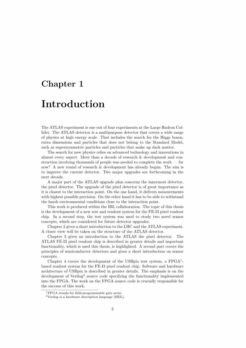
2.1 The LHC AcceleratorThe Large Hadron Collider (LHC, see figure 2.1) is the world’s largest circu-lar collider located at the international research facility CERN1, the EuropeanOrganization for Nuclear Research. The LHC was built into the tunnel of theformer Large Electron-Positron Collider (LEP). The tunnel has a circumfer-ence of 27 km and is sited approximately 100 m beneath the surface and wasextended to house new experiments at the LHC. The accelerator ring consistsof large superconducting magnets and accelerator structures designed to boostproton pairs up to a center-of-mass energy of
Ôs = 14 TeV. Counter-rotating
bunches of particles just mentioned are brought to collision at four distinct in-teraction points distributed along the accelerator ring. The particle bunches arecolliding up to 40, 000, 000 times per second, which corresponds to the bunchcrossing frequency of 40 MHz. Four large detectors (ALICE, ATLAS, CMS andLHCb) are built around these collision points.
Figure 2.1: The Large Hadron Collider and its underground structures [1].
1European Organization for Nuclear Research CERN, CH-1211, Genève 23, Switzerland.
5
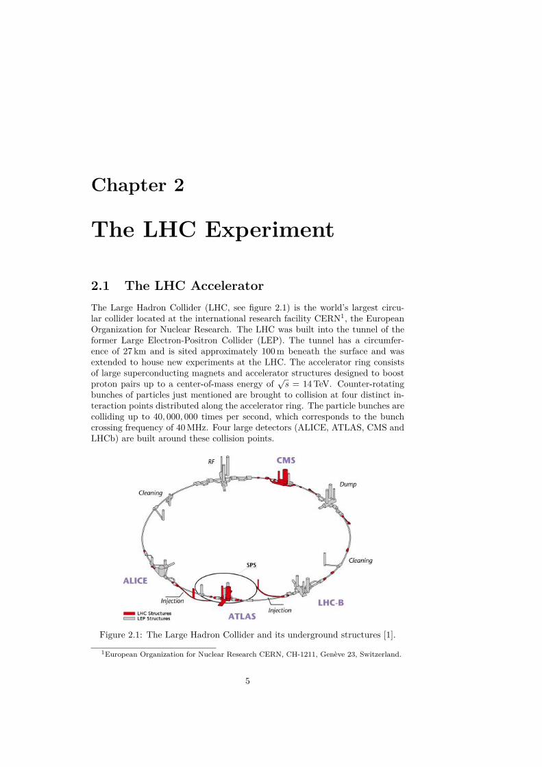
2.2 The ATLAS DetectorThe ATLAS detector [2] (see figure 2.2) is one out of four detectors along theLHC accelerator ring, and is one out of two multipurpose collider detectors thatcovers a wide range of physics. It was designed to investigate proton-proton andion-ion interactions at TeV energy scale. The detector is situated inside a cavern80 m underground and has a diameter of 25 m and a length of 44 m. The particlecollisions take place at the center of the detector. Due to the forward-backwardsymmetry of two colliding beams, the detector has a cylindrical shape along thebeam axis.
Figure 2.2: Cut-away view of the ATLAS detector. The LHC accelerator ringis extended in either horizontal direction.
The following points are crucial to meet the experimental challenges: a pre-cise energy measurement, a precise momentum measurement, a possibility forparticle identification and a hermetic design that covers a wide pseudorapid-ity2 range to allow high particle detection e�ciency. This is achieved by sixdi�erent detector subsystems that identify particles and measure either theirmomentum or energy. To make the determination of the momentum possible,a solenoid, a barrel toroid and two end-cap toroids produce a magnetic field tobend the trajectory of charged particles. The measurement of the momentumis accompanied by precise track reconstruction.
A multi-stage trigger system reduces the event data recording rate to alevel that does not exceed the limits of the data storage infrastructure. Aproton-proton interaction rate of 1 GHz is expected at the design luminosity of1◊1034 cm≠2s≠1. First, a fast trigger system that uses a small subset of availabledetector information (from calorimeter and muon detector) decides on whetheror not to continue processing an event. The so-called Level-1 trigger system
2Pseudorapidity ÷ is a coordinate to describe the angle ◊ of a particle trajectory withrespect to the beam axis: ÷ = ≠ ln(tan ◊
2
). The pseudorapidity is independent of Lorentzboost along the beam axis.
6
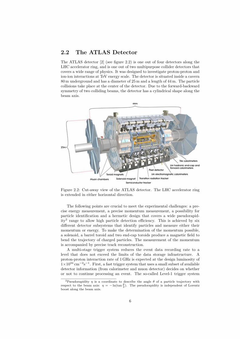
Figure 2.3: Cut-away view of the inner detector. The inner detector is composedof the following sub-detectors in successive order: the pixel detector close tothe beam pipe, the silicon microstrip detector (SCT) and transition radiationdetector (TRT). The inner detector is enclosed by a solenoid (not shown in thefigure).
reduces the event data rate to approximately 100 kHz. Finally, two higher leveltriggers, the Level-2 trigger and the event filter, further reduce the data takingrate to approximately 200 Hz.
2.2.1 The Inner DetectorFigure 2.3 gives an overview about the structure of the inner detector. Themulti-layered structure comprises, from the inside to the outside, the followingthree successive sub-detectors: the pixel detector close to the beryllium beampipe, the silicon microstrip detector and the transition radiation detector. Theinner detector is enclosed by a solenoid, which generates an axial magnetic fieldof approximately 2 T, to bend the trajectories of charged collision products andthus enable the measurement of their momentum.
The main purpose of the inner detector is the precise determination of themomentum of charged particles. It was also built to provide a hermetic patternrecognition and precise primary and secondary vertex measurements within apseudorapidity range of |÷| = 2.5 (◊ = 9.4°) and particle identification within|÷| = 2.0 (◊ = 15.4°).
A particle has to interact with the detector material to determine its trajec-tory. This happens at discrete points within the detector at di�erent distancesfrom the place of origin e. g. the primary vertex of a collision inside the beampipe. The pixels detector is placed closest to beam pipe. There, it can deliver thehighest single point resolution (and thus very good pattern recognition) within
7
all sub-detectors. Such a high single point resolution is necessary to competewith the high particle occupancy due to the enormous particle flux close to theinteraction point. To maintain the pixel detector operable at high radiationdose it must be kept at low temperature (approximately ≠5°C to ≠10°C). Theinnermost layer (or b-layer3 ) has an expected lifetime of 3 years at LHC designluminosity. Beside the b-layer two other pixel layers and three end-cap diskson either side of the cylinder encloses the collision point. They are expectedto withstand the particle flux over the operational lifetime of the experiment.More details on the pixel detector will be given in chapter 3.
A second sub-detector is built around pixel detector: the silicon microstripdetector (SCT). Its purpose is the same as that of the pixel detector: measure-ment of the momentum and pattern recognition. The SCT consists of four barrellayers and nine end-cap disks on either side. Each layer and disc is equippedwith back-to-back sensors that have a stereo angle of 40 mrad to obtain two-dimensional spatial resolution. The strip pitch is 80 µm for the barrel sensorsand for the disks between 57 µm and 90 µm due to the geometry. This resultsin an intrinsic resolution of 17 µm in R-„-direction and 580 µm in z-direction(barrel) or R-direction (disks). To withstand the harsh environment the SCTis also kept at the same temperature as the pixel detector.
At larger radii, the transition radiation tracker (TRT) provides trackinginformation of particles that traverse many layers of close-packed drift strawtube elements of 4 mm in diameter. The straws (cathode) are filled with non-flammable gas mixture of 70% Xe, 27% CO
2
and 3% O2
. Each straw is equippedwith an anode wire (the sense wire) that is placed in the center. Each tubeprovides a drift time measurement, giving a spatial resolution of 170 µm. Twoindependent thresholds are applied to every readout channel to discriminatebetween tracking hits, which pass the lower threshold, and transition radiationhits, which pass the higher one. The barrel is built up from axially orientedstraws (approximately 50, 000) whereas both end-cap wheels contain radiallyoriented straws (approximately 320, 000). The entire sub-detector is designed tooperate at room temperature and is surrounded by CO
2
to avoid pollution of thestraws. With an average of 36 hits per crossing particle, it enhances the patternrecognition, improves the momentum resolution and provides electron/positronidentification.
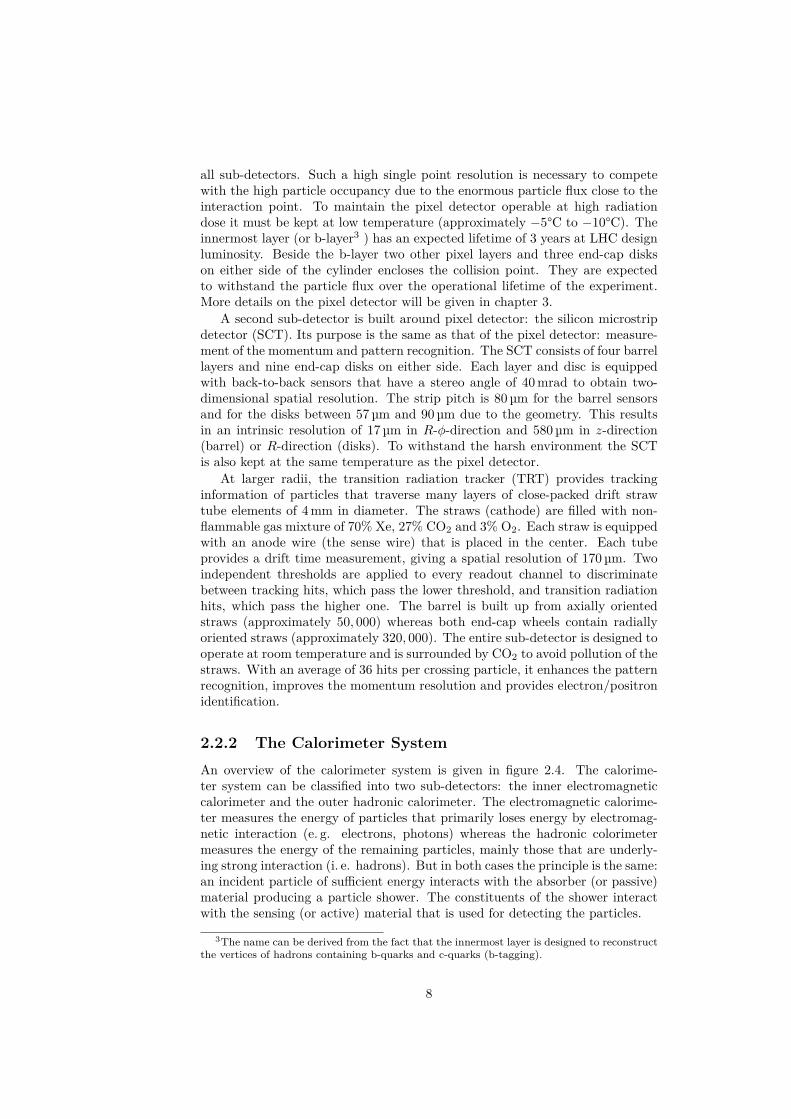
2.2.2 The Calorimeter SystemAn overview of the calorimeter system is given in figure 2.4. The calorime-ter system can be classified into two sub-detectors: the inner electromagneticcalorimeter and the outer hadronic calorimeter. The electromagnetic calorime-ter measures the energy of particles that primarily loses energy by electromag-netic interaction (e. g. electrons, photons) whereas the hadronic colorimetermeasures the energy of the remaining particles, mainly those that are underly-ing strong interaction (i. e. hadrons). But in both cases the principle is the same:an incident particle of su�cient energy interacts with the absorber (or passive)material producing a particle shower. The constituents of the shower interactwith the sensing (or active) material that is used for detecting the particles.
3The name can be derived from the fact that the innermost layer is designed to reconstructthe vertices of hadrons containing b-quarks and c-quarks (b-tagging).
8
The electromagnetic calorimeter uses lead as absorber material and liquidargon (LAr) as sensing material. Particles of the shower liberate electrons fromthe argon atoms. Liquid argon act as a conductor and therefore the electronscan be collected by electrodes and are read out.
The electromagnetic calorimeter has a particular geometry: the accordion-shaped (or folded) absorbers and electrodes allow having several active layersin depth. This is beneficial for the energy resolution which is in the order of‡(E)/E = 10%/
ÔE [3]. A spatial resolution is obtained by segmenting the first
layer.
The hadronic calorimeter is divided into three parts: the tile and tile ex-tended barrel calorimeter, the LAr hadronic end-cap calorimeter (HEC) andthe LAr forward calorimeter (FCAL). The both latter are using liquid argon assensing material. The end-cap calorimeter uses copper (Cu) as passive materialwhereas the FCAL uses both, copper and tungsten (W). The tile barrel is madeof steel with scintillating tiles in between. The light signals are read out byphotomultiplier tubes.
Pion measurements show that the energy resolution ‡(E)/E is of approx-imately 50%/
ÔE for the tile barrel calorimeter, 90%/
ÔE for the HEC and
70%/
ÔE for the FCAL [3].
Figure 2.4: Cut-away view of the calorimeter system. The inner detector is in-dicated at the center and is enclosed by the electromagnetic calorimeter (liquidargon electromagnetic barrel and end-cap). The hadronic calorimeter (tile bar-rel, tile extended barrel, liquid argon hadronic end-cap and liquid-argon forwardcalorimeter) is built around the electromagnetic colorimeter. The part of liquid-argon forward calorimeter, which uses copper absorbers, is an electromagneticcalorimeter, while the part, which uses tungsten, is a hadronic calorimeter. Acryostat is required to keep the argon liquid.
9
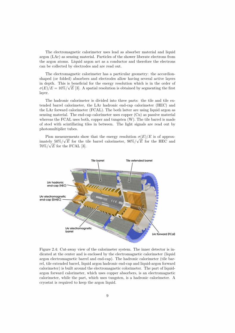
Figure 2.5: Cut-away view of the muon spectrometer. The nested structure ofthe tracking chambers minimizes the gaps in detector coverage.
2.2.3 The Muon SpectrometerThe muon spectrometer, as shown in figure 2.5, forms the outer part of the AT-LAS detector and is the largest sub-detector in size. The tracking chambers ofthe muon sub-detector detect charged particles that exit the calorimeter. Thisare in most cases muons which live long enough to reach the outer regions ofthe detector. A barrel toroid and the two end-cap toroids generate a large-scale toroidal magnetic field of approximately 0.5 T and 1 T respectively. Thusmakes it is possible to measure the momentum of charged particles in the pseu-dorapidity range of |÷| < 2.7. The transverse momentum (p
T
) resolution is ofapproximately 10% for 1 TeV particles.
In the barrel region, precision-tracking chambers are located on and betweenthe eight coils of the barrel toroid. The nested chambers are arranged in threecylindrical layers at radii of approximately 5, 7.5 and 10 m. In the end-capregion, several muon chambers form large disks. The end-cap disks are locatedin front and behind each end-cap toroid at a distance of 7.4, 10.8, 14 and 21.5 mfrom the collision point.
The muon spectrometer is essential for the search of new physics. It isdesigned to deliver a fast trigger on particles in the pseudorapidity range of|÷| < 2.4. The trigger occurs if a certain transverse momentum threshold isexceeded.
10
Chapter 3
Silicon Pixel Detectors
3.1 IntroductionThis chapter will give an introduction on the ATLAS pixel vertex detector andthe FE-I3 pixel readout chip (sections 3.2 and 3.3, respectively). The purpose ofa vertex detector is to reconstruct the primary and secondary vertices of hadronscontaining b- and c-quarks. The vertices are reconstructed by extrapolating thehit information measured by several detector layers around the interaction point.The high single point resolution and tracking e�ciency of a pixel detector arerequired to obtain better tagging e�ciency of the jet flavor. Also, in order tocope with the harsh environment close to the collision point, a pixel detectorhas an advantage of low per-pixel hit occupancy and per-pixel leakage currentand thus noise.
In sum, the following criteria must be met by a modern pixel vertex detector:
• The innermost vertex layer should be as close to the collision point aspossible to increase the accuracy of the vertex and impact parameter re-construction.
• The detector and its components should be based on a radiation-hardeneddesign.
• The material budget (in radiation length) of the detector and its support-ing structures should be as low as possible to reduce the e�ect of multiplescattering. This is particularly important for the innermost detector layer.
• The pixel detector should have a high spatial resolution in order to providea good hit resolution. Low noise and low hit occupancy are also impor-tant qualities for pattern recognition and for finding primary/secondaryvertices [4] in a high multiplicity environment (e. g. nearby tracks in ajet).
• Hermetic coverage over a wide pseudorapidity range.
In a second part (section 3.4) and in a more general approach, the e�ect of ra-diation on silicon will be discussed. In section 3.4.1, the interaction of ionizingparticles with the sensor material will be explained and thus the generation ofcharge that is detected as electrical signal. Section 3.4.2 will highlight another
11
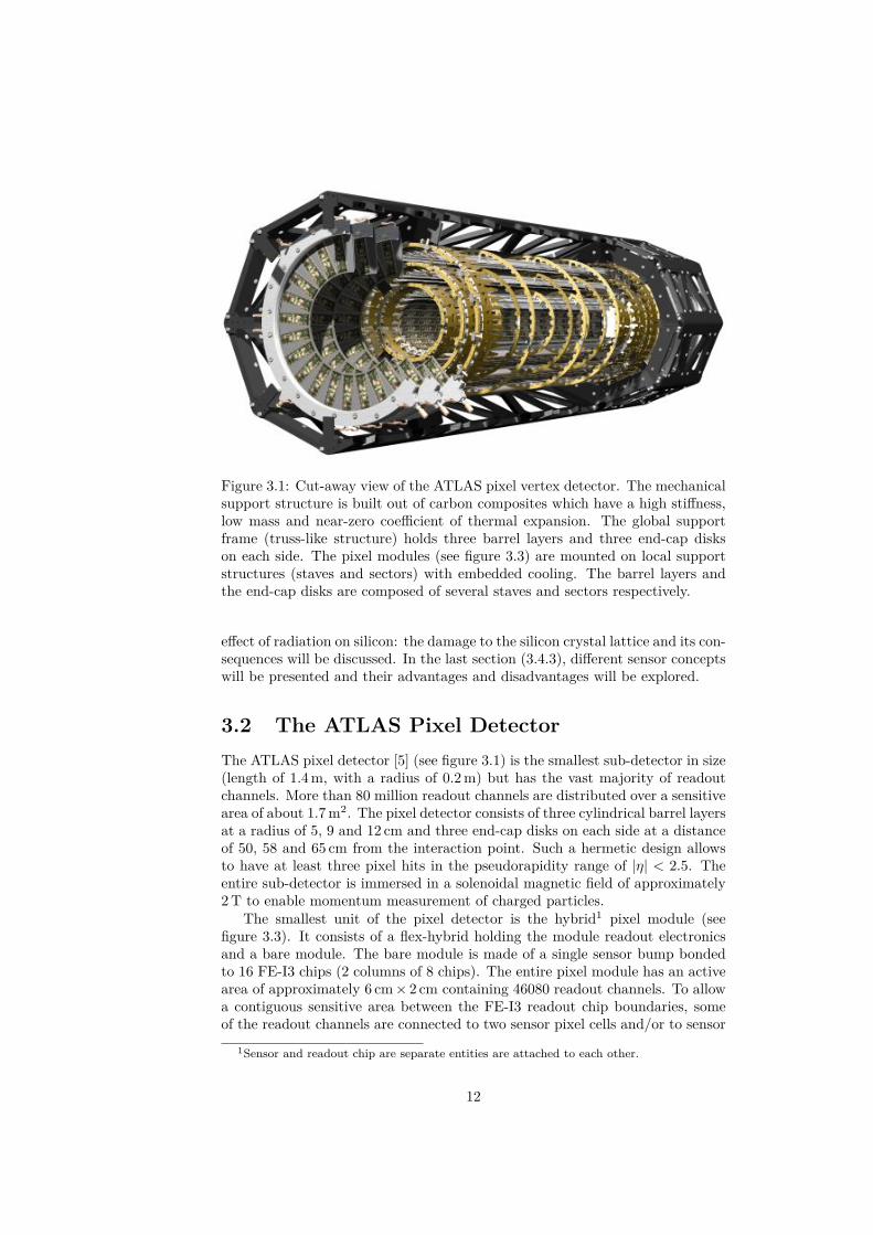
Figure 3.1: Cut-away view of the ATLAS pixel vertex detector. The mechanicalsupport structure is built out of carbon composites which have a high sti�ness,low mass and near-zero coe�cient of thermal expansion. The global supportframe (truss-like structure) holds three barrel layers and three end-cap diskson each side. The pixel modules (see figure 3.3) are mounted on local supportstructures (staves and sectors) with embedded cooling. The barrel layers andthe end-cap disks are composed of several staves and sectors respectively.
e�ect of radiation on silicon: the damage to the silicon crystal lattice and its con-sequences will be discussed. In the last section (3.4.3), di�erent sensor conceptswill be presented and their advantages and disadvantages will be explored.
3.2 The ATLAS Pixel DetectorThe ATLAS pixel detector [5] (see figure 3.1) is the smallest sub-detector in size(length of 1.4 m, with a radius of 0.2 m) but has the vast majority of readoutchannels. More than 80 million readout channels are distributed over a sensitivearea of about 1.7 m2. The pixel detector consists of three cylindrical barrel layersat a radius of 5, 9 and 12 cm and three end-cap disks on each side at a distanceof 50, 58 and 65 cm from the interaction point. Such a hermetic design allowsto have at least three pixel hits in the pseudorapidity range of |÷| < 2.5. Theentire sub-detector is immersed in a solenoidal magnetic field of approximately2 T to enable momentum measurement of charged particles.
The smallest unit of the pixel detector is the hybrid1 pixel module (seefigure 3.3). It consists of a flex-hybrid holding the module readout electronicsand a bare module. The bare module is made of a single sensor bump bondedto 16 FE-I3 chips (2 columns of 8 chips). The entire pixel module has an activearea of approximately 6 cm ◊ 2 cm containing 46080 readout channels. To allowa contiguous sensitive area between the FE-I3 readout chip boundaries, someof the readout channels are connected to two sensor pixel cells and/or to sensor
1Sensor and readout chip are separate entities are attached to each other.
12
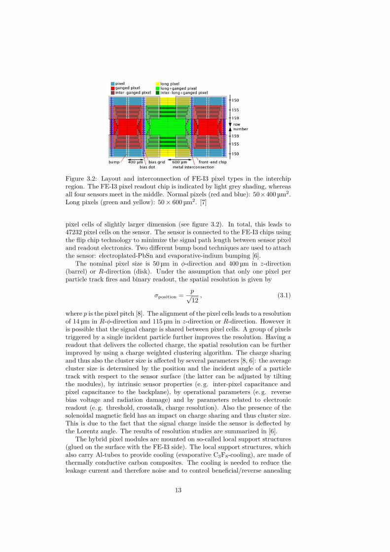
Figure 3.2: Layout and interconnection of FE-I3 pixel types in the interchipregion. The FE-I3 pixel readout chip is indicated by light grey shading, whereasall four sensors meet in the middle. Normal pixels (red and blue): 50◊400 µm2.Long pixels (green and yellow): 50 ◊ 600 µm2. [7]
pixel cells of slightly larger dimension (see figure 3.2). In total, this leads to47232 pixel cells on the sensor. The sensor is connected to the FE-I3 chips usingthe flip chip technology to minimize the signal path length between sensor pixeland readout electronics. Two di�erent bump bond techniques are used to attachthe sensor: electroplated-PbSn and evaporative-indium bumping [6].
The nominal pixel size is 50 µm in „-direction and 400 µm in z-direction(barrel) or R-direction (disk). Under the assumption that only one pixel perparticle track fires and binary readout, the spatial resolution is given by
‡
position
= pÔ12
, (3.1)
where p is the pixel pitch [8]. The alignment of the pixel cells leads to a resolutionof 14 µm in R-„-direction and 115 µm in z-direction or R-direction. However itis possible that the signal charge is shared between pixel cells. A group of pixelstriggered by a single incident particle further improves the resolution. Having areadout that delivers the collected charge, the spatial resolution can be furtherimproved by using a charge weighted clustering algorithm. The charge sharingand thus also the cluster size is a�ected by several parameters [8, 6]: the averagecluster size is determined by the position and the incident angle of a particletrack with respect to the sensor surface (the latter can be adjusted by tiltingthe modules), by intrinsic sensor properties (e. g. inter-pixel capacitance andpixel capacitance to the backplane), by operational parameters (e. g. reversebias voltage and radiation damage) and by parameters related to electronicreadout (e. g. threshold, crosstalk, charge resolution). Also the presence of thesolenoidal magnetic field has an impact on charge sharing and thus cluster size.This is due to the fact that the signal charge inside the sensor is deflected bythe Lorentz angle. The results of resolution studies are summarized in [6].
The hybrid pixel modules are mounted on so-called local support structures(glued on the surface with the FE-I3 side). The local support structures, whichalso carry Al-tubes to provide cooling (evaporative C
3
F8
-cooling), are made ofthermally conductive carbon composites. The cooling is needed to reduce theleakage current and therefore noise and to control beneficial/reverse annealing
13
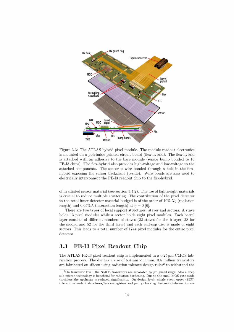
Figure 3.3: The ATLAS hybrid pixel module. The module readout electronicsis mounted on a polyimide printed circuit board (flex-hybrid). The flex-hybridis attached with an adhesive to the bare module (sensor bump bonded to 16FE-I3 chips). The flex-hybrid also provides high-voltage and low-voltage to theattached components. The sensor is wire bonded through a hole in the flex-hybrid exposing the sensor backplane (p-side). Wire bonds are also used toelectrically interconnect the FE-I3 readout chip to the flex-hybrid.
of irradiated sensor material (see section 3.4.2). The use of lightweight materialsis crucial to reduce multiple scattering. The contribution of the pixel detectorto the total inner detector material budged is of the order of 10% X
0
(radiationlength) and 0.05% ⁄ (interaction length) at ÷ = 0 [6].
There are two types of local support structures: staves and sectors. A staveholds 13 pixel modules while a sector holds eight pixel modules. Each barrellayer consists of di�erent numbers of staves (22 staves for the b-layer, 38 forthe second and 52 for the third layer) and each end-cap disc is made of eightsectors. This leads to a total number of 1744 pixel modules for the entire pixeldetector.
3.3 FE-I3 Pixel Readout ChipThe ATLAS FE-I3 pixel readout chip is implemented in a 0.25 µm CMOS fab-rication process. The die has a size of 5.4 mm ◊ 11 mm. 3.5 million transistorsare fabricated on silicon using radiation tolerant design rules2 to withstand the
2On transistor level: the NMOS transistors are separated by p+ guard rings. Also a deepsub-micron technology is beneficial for radiation hardening. Due to the small MOS gate oxidethickness the upcharge is reduced significantly. On design level: single event upset (SEU)tolerant redundant structures/blocks/registers and parity checking. For more information see
14
(a) (b)
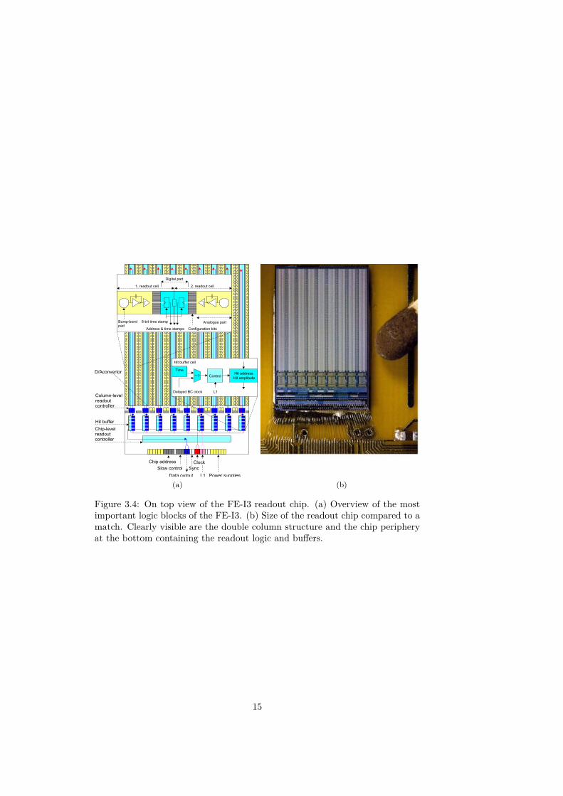
Figure 3.4: On top view of the FE-I3 readout chip. (a) Overview of the mostimportant logic blocks of the FE-I3. (b) Size of the readout chip compared to amatch. Clearly visible are the double column structure and the chip peripheryat the bottom containing the readout logic and bu�ers.
15
required radiation tolerance up to a total dose of 50 Mrad. The chip contains2880 readout channels arranged in matrix of 160 rows ◊ 18 columns. The sizeof each readout cell is 50 µm ◊ 400 µm (row-to-row pitch ◊ column-to-columnpitch). The power consumption should be less than 40 µW per readout channelto fulfill the design requirements [11]. However, the chip typically draws 40 mAof current from a 2 V (digital supply voltage) supply and 80 mA of current froma 1.6 V (analog supply voltage) supply (see also [12]), which is 30 µW abovedesign requirements per readout channel.
Figure 3.4 shows the most important logic blocks of the FE-I3. Each pixelconsists of an analog and a digital block. The task of the analog pixel blockis to amplify and shape the input signal charge which is generated by particleshitting the sensor. The digital block comprises all digital elements beginningfrom the digital pixel block and ending at the readout controller in the chipperiphery. The digital pixel block communicates with the logic located in thechip periphery and transmits the hit data. The 18 pixel columns are alignedto 9 double columns. The double column comprises 320 readout channels, eachsharing the same column bus, column arbitration unit (CAU, also referred to ascolumn readout controller) and end-of-column (EoC) bu�er. Beside the doublecolumn readout logic (CAU and EoC bu�er), also the chip level readout con-troller (ROC) is located in the chip periphery. The ROC collects the hit dataand sends them out serially. The following sections will give a more detaileddescription about the analog and digital design.
3.3.1 Chip ConfigurationThe FE-I3 readout chip has a 14-bit local configuration register which is locatedin each of the 2880 pixel readout blocks. Also 231-bit long global configurationregister exists. Parts of the global configuration register are located underneaththe pixel matrix and in the chip periphery in vicinity of the corresponding logicblocks. All configuration bits are stored in single event upset (SEU) tolerantlatches/RAM cells.
The latches can be accessed by using two long shift register. One 231-bitlong shit register for the global register and one 2880-bit long shift register foraccessing the pixel register bits.
An additional 29-bit long command register controls the shifting of the bitpattern and the latching of the bits into the corresponding RAM cells. Thecommand register determines into which shift register the received bit patternis shifted. It also determines into which local register the pixel shift register islatched.
Three input signals are needed: command clock (CCK), data input (DI)and a load signal (LD). The clock is sent in parallel with data: DI must besynchronous to the CCK and the CCK is enabled only during shifting the data.
The procedure is as follows: first, the 29-bit command has to be written tothe command register to get access the intended configuration register (clockcommand). When LD is low the command data can be shifted into the commandregister (CCK enabled for 29 clock cycles). To latch the command data, LDmust be asserted. Immediately, the command becomes active. Second, theconfiguration data is shifted to the shift register. The LD stays asserted and
[8, 9, 10, 11].
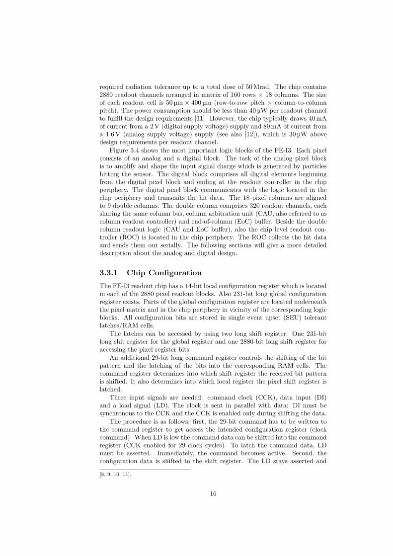
16
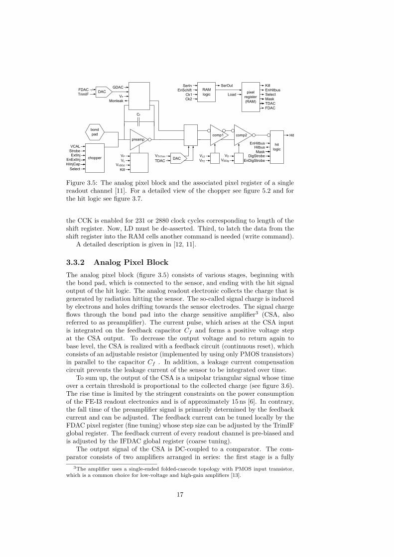
Figure 3.5: The analog pixel block and the associated pixel register of a singlereadout channel [11]. For a detailed view of the chopper see figure 5.2 and forthe hit logic see figure 3.7.
the CCK is enabled for 231 or 2880 clock cycles corresponding to length of theshift register. Now, LD must be de-asserted. Third, to latch the data from theshift register into the RAM cells another command is needed (write command).
A detailed description is given in [12, 11].
3.3.2 Analog Pixel BlockThe analog pixel block (figure 3.5) consists of various stages, beginning withthe bond pad, which is connected to the sensor, and ending with the hit signaloutput of the hit logic. The analog readout electronic collects the charge that isgenerated by radiation hitting the sensor. The so-called signal charge is inducedby electrons and holes drifting towards the sensor electrodes. The signal chargeflows through the bond pad into the charge sensitive amplifier3 (CSA, alsoreferred to as preamplifier). The current pulse, which arises at the CSA inputis integrated on the feedback capacitor C
f
and forms a positive voltage stepat the CSA output. To decrease the output voltage and to return again tobase level, the CSA is realized with a feedback circuit (continuous reset), whichconsists of an adjustable resistor (implemented by using only PMOS transistors)in parallel to the capacitor C
f
. In addition, a leakage current compensationcircuit prevents the leakage current of the sensor to be integrated over time.
To sum up, the output of the CSA is a unipolar triangular signal whose timeover a certain threshold is proportional to the collected charge (see figure 3.6).The rise time is limited by the stringent constraints on the power consumptionof the FE-I3 readout electronics and is of approximately 15 ns [6]. In contrary,the fall time of the preamplifier signal is primarily determined by the feedbackcurrent and can be adjusted. The feedback current can be tuned locally by theFDAC pixel register (fine tuning) whose step size can be adjusted by the TrimIFglobal register. The feedback current of every readout channel is pre-biased andis adjusted by the IFDAC global register (coarse tuning).
The output signal of the CSA is DC-coupled to a comparator. The com-parator consists of two amplifiers arranged in series: the first stage is a fully
3The amplifier uses a single-ended folded-cascode topology with PMOS input transistor,which is a common choice for low-voltage and high-gain amplifiers [13].
17
Figure 3.6: Output of the charge sensitive amplifier (CSA). The unipolar trian-gular signal, whose time over a certain threshold is proportional to the collectedcharge, is DC-coupled to the comparator.
di�erential low-gain amplifier and the second stage is a classical two-stage dif-ferential amplifier [13]. The comparator compares the output signal of the CSAto a well-defined threshold potential. The reason for this is as follows: the baseline potential of the CSA output depends on VDD
ref
4. VDDref
is also usedto generate the threshold potential (often referred to as V
replica
). Then, thethreshold is defined as the di�erence between the threshold potential and baseline potential. The threshold potential is generated locally to avoid variationsin threshold across the chip. Again, the threshold potential can be adjustedlocally by setting the TDAC pixel register (fine tuning) and globally by set-ting the GDAC global register (coarse tuning). The step size of the TDAC isadjusted by the TrimTh global register.
In the moment when the output signal of the CSA exceeds the threshold po-tential, the comparator asserts the binary hit signal. The hit signal is de-assertedwhen output signal falls below the threshold. Consequently, the length of the hitsignal depends on the feedback current and threshold and is proportional to thecollected charge. The time the signal is asserted is called Time-over-Threshold(ToT).
The hit signal is received to the hit logic (see figure 3.7). The hit signalis sent to the hitbus if the WriteHitbus pixel register is set. The hitbus canbe asserted by any of the 2880 readout channels (OR’ed). The hitbus signalcan be used internally for self-triggering or can be read out from a pad on theFE-I3 readout chip. A second output (indicated as “Hit”) is connected to thedigital pixel block. The transmission of the hit signal to the digital block canbe disabled by setting the WriteMask pixel register bit to 1.
In addition, each readout channel has a separate charge injection mechanism(indicated as “chopper” in figure 3.5), which is used to adjust the feedbackcurrent of the CSA and the threshold of the comparator. The charge injectioncircuit is topic of section 5.4.
4As well as on the bias current of the amplifier.
18
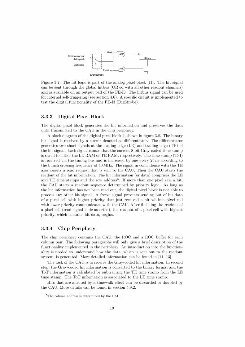
Figure 3.7: The hit logic is part of the analog pixel block [11]. The hit signalcan be sent through the global hitbus (OR’ed with all other readout channels)and is available on an output pad of the FE-I3. The hitbus signal can be usedfor internal self-triggering (see section 4.6). A specific circuit is implemented totest the digital functionality of the FE-I3 (DigStrobe).
3.3.3 Digital Pixel BlockThe digital pixel block generates the hit information and preserves the datauntil transmitted to the CAU in the chip periphery.
A block diagram of the digital pixel block is shown in figure 3.8. The binaryhit signal is received by a circuit denoted as di�erentiator. The di�erentiatorgenerates two short signals at the leading edge (LE) and trailing edge (TE) ofthe hit signal. Each signal causes that the current 8-bit Gray-coded time stampis saved to either the LE RAM or TE RAM, respectively. The time stamp (TSI)is received via the timing bus and is increased by one every 25 ns according tothe bunch crossing frequency of 40 MHz. The signal in coincidence with the TEalso asserts a read request that is sent to the CAU. Then the CAU starts thereadout of the hit information. The hit information (or data) comprises the LEand TE time stamps and the row address5. If more than one pixel saw a hit,the CAU starts a readout sequence determined by priority logic. As long asthe hit information has not been read out, the digital pixel block is not able toprocess any other hit signal. A freeze signal prevents sending out of hit dataof a pixel cell with higher priority that just received a hit while a pixel cellwith lower priority communicates with the CAU. After finishing the readout ofa pixel cell (read signal is de-asserted), the readout of a pixel cell with highestpriority, which contains hit data, begins.
3.3.4 Chip PeripheryThe chip periphery contains the CAU, the ROC and a EOC bu�er for eachcolumn pair. The following paragraphs will only give a brief description of thefunctionality implemented in the periphery. An introduction into the function-ality is needed to understand how the data, which is sent out to the readoutsystem, is generated. More detailed information can be found in [11, 13].
The task of the CAU is to receive the Gray-coded hit information. In secondstep, the Gray-coded hit information is converted to the binary format and theToT information is calculated by subtracting the TE time stamp from the LEtime stamp. The ToT information is associated to the LE time stamp.
Hits that are a�ected by a timewalk e�ect can be discarded or doubled bythe CAU. More details can be found in section 5.9.2.
5The column address is determined by the CAU.
19
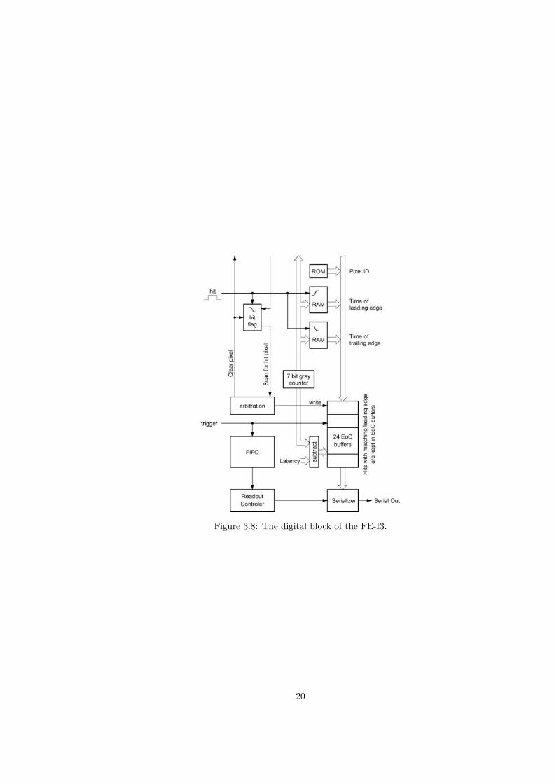
Figure 3.8: The digital block of the FE-I3.
20
hits/DC/BC0 0.5 1 1.5 2 2.5 3 3.5 4 4.5 5
Inef
ficie
ncy
0
0.1
0.2
0.3
0.4
0.5
0.6
0.7
0.8
0.9
1
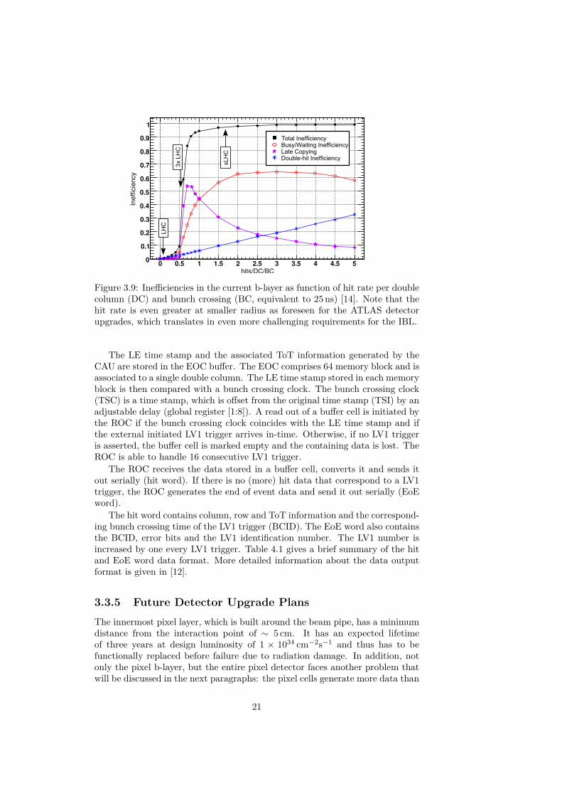
Figure 3.9: Ine�ciencies in the current b-layer as function of hit rate per doublecolumn (DC) and bunch crossing (BC, equivalent to 25 ns) [14]. Note that thehit rate is even greater at smaller radius as foreseen for the ATLAS detectorupgrades, which translates in even more challenging requirements for the IBL.
The LE time stamp and the associated ToT information generated by theCAU are stored in the EOC bu�er. The EOC comprises 64 memory block and isassociated to a single double column. The LE time stamp stored in each memoryblock is then compared with a bunch crossing clock. The bunch crossing clock(TSC) is a time stamp, which is o�set from the original time stamp (TSI) by anadjustable delay (global register [1:8]). A read out of a bu�er cell is initiated bythe ROC if the bunch crossing clock coincides with the LE time stamp and ifthe external initiated LV1 trigger arrives in-time. Otherwise, if no LV1 triggeris asserted, the bu�er cell is marked empty and the containing data is lost. TheROC is able to handle 16 consecutive LV1 trigger.
The ROC receives the data stored in a bu�er cell, converts it and sends itout serially (hit word). If there is no (more) hit data that correspond to a LV1trigger, the ROC generates the end of event data and send it out serially (EoEword).
The hit word contains column, row and ToT information and the correspond-ing bunch crossing time of the LV1 trigger (BCID). The EoE word also containsthe BCID, error bits and the LV1 identification number. The LV1 number isincreased by one every LV1 trigger. Table 4.1 gives a brief summary of the hitand EoE word data format. More detailed information about the data outputformat is given in [12].
3.3.5 Future Detector Upgrade PlansThe innermost pixel layer, which is built around the beam pipe, has a minimumdistance from the interaction point of ≥ 5 cm. It has an expected lifetimeof three years at design luminosity of 1 ◊ 1034 cm≠2s≠1 and thus has to befunctionally replaced before failure due to radiation damage. In addition, notonly the pixel b-layer, but the entire pixel detector faces another problem thatwill be discussed in the next paragraphs: the pixel cells generate more data than
21
the digital readout of the chip can cope with.The LHC is planned to be upgraded to higher luminosity. This happens in
two steps: with a first upgrade estimated in 2016, it is planned to reach peakluminosity 2 to 3 times higher than the current design luminosity. In a secondstep, the luminosity will be increased to approximately 10 times the initialluminosity in a more ambitious upgrade. This upgrade is commonly referredto as HL-LHC6 (or sLHC) and is currently scheduled for completion at thebeginning of the next decade.
This higher luminosity leads to new problems that arise from the fact thatthe double column ine�ciency of the ATLAS FE-I3 pixel readout chips increasesdrastically with the hit occupancy [14]. Figure 3.9 shows the progression of theine�ciency and points out why FE-I3 pixel readout chip cannot cope with higherluminosity as it is foreseen. The following points contribute to the ine�ciency:
Double-hit ine�ciency Two temporally close hits to a given pixel cannot beresolved. After a hit, the pixel is busy for a certain amount of time untilthe data transfer is finished. A second hit can also results in a pile-up ofthe first hit.
Busy/Waiting ine�ciency At high luminosity the double column bus be-comes saturated. This increases the time it takes for a pixel to start copy-ing data to the double column bu�er. While waiting for double columnbus to become free, the pixel gets a second hit that cannot be stored.
Late copying ine�ciency At high luminosity the double column bus be-comes saturated. The increase in time it takes for a pixel to copy datato the double column bu�er results in the loss of hit information. Thehit information has not arrived at the double column bu�er in time to beread out synchronous to the Level-1 trigger.
One possible solution is the reduction of the pixel size. A smaller pixel cell sizecan cope with a higher luminosity due to lower per-pixel occupancy and willalso have a benefit on tracking resolution. The ine�ciency related to the datatransfer in the double-columns can be overcome by a new digital design of thereadout chip. The e�ort of a new ATLAS readout chip (FE-I4A) has started in2008 [15] and a full-sized prototype is currently under investigation.
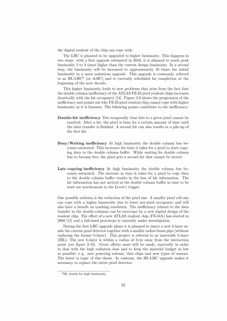
During the first LHC upgrade phase it is planned to insert a new b-layer in-side the current pixel detector together with a smaller radius beam pipe (withoutreplacing the former b-layer). This project is referred to as insertable b-layer(IBL). The new b-layer is within a radius of 3 cm away from the interactionpoint (see figure 3.10). Great e�orts must still be made, especially in orderto deal with the high radiation dose and to keep the material budget as lowas possible, e. g. new powering scheme, thin chips and new types of sensors.The latter is topic of this thesis. In contrast, the HL-LHC upgrade makes itnecessary to replace the entire pixel detector.
6HL stands for high luminosity.
22
(a)
(b)
Figure 3.10: a) The ATLAS pixel detector before the IBL upgrade. (I) denotesthe current b-layer. b) The ATLAS pixel detector after insertion of the newb-layer which is based on the FE-I4 readout chip (II). The former b-layer staysinside the detector.
3.4 Semiconductor Pixel Sensors in HEP Exper-iments
Semiconductor detectors are widely used in high energy physics (HEP) exper-iments to detect ionizing radiation. Semiconductor detectors use a semicon-ductor sensor material to detect ionizing radiation (i.e. charged particles andphotons). They are using a broad spectrum of di�erent sensor materials, e.g.silicon (Si), gallium arsenide (GaAs) and Diamond7, which have one thing incommon: a band gap. Charged particles, which interact with the sensor ma-terial, generate free charge carriers. The energy needed to create electron-holepairs varies with the sensitive material being used but is still low comparedto the energy required for production electron-ion pairs in a gaseous detector(even for Diamond8). Hence, in semiconductor detectors the statistical fluctua-tions of the deposited energy are smaller and thus the spread of the signal pulseheight. This leads to a better energy resolution compared to a gaseous detector.Also the time resolution is better for the following reasons: free charge carriers,especially electrons, have a high mobility and thus a high drift velocity for agiven electric field strength: v
d
= µE, where v
d
denotes drift velocity, µ mo-bility, and E the magnitude of the electric field. Fast charge carriers travellingtowards their readout electrode, decrease the rise time of the induced signal(Ramo theorem, see following section).
The simplest semiconductor detector imaginable is a single PIN diode. How-ever, todays detectors consist of thousands of individual readout channels whichare densely packed on a chip of a few cm2 in size. Such detectors have a hightracking resolution compared to other technologies such as wire chambers. Thedisadvantages of semiconductor detectors are the high costs for large-volumetracker detectors and the requirement of sophisticated cooling technology to re-duce leakage currents and thus noise. In addition, in semiconductor detectors,
7Normally considered as an insulator.8Mean ionization energy [16]: 3.62 eV for silicon, 13.1 eV for diamond and 20...30 eV for a
gaseous detector.
23
Muon momentum p
1
10
100S
top
pin
g p
ower
[M
eV c
m2/g
]
Li n
dh
ar d
-S
charf
f
Bethe-Bloch Radiative
Radiativeeffects
reach 1%
Without !
Radiativelosses
"#0.001 0.01 0.1 1 10 100
1001010.1
1000 104
105
106
[MeV/c]
100101
[GeV/c]
100101
[TeV/c]
Andersen-Ziegler
Minimumionization
Eµc
µ!
Nuclearlosses
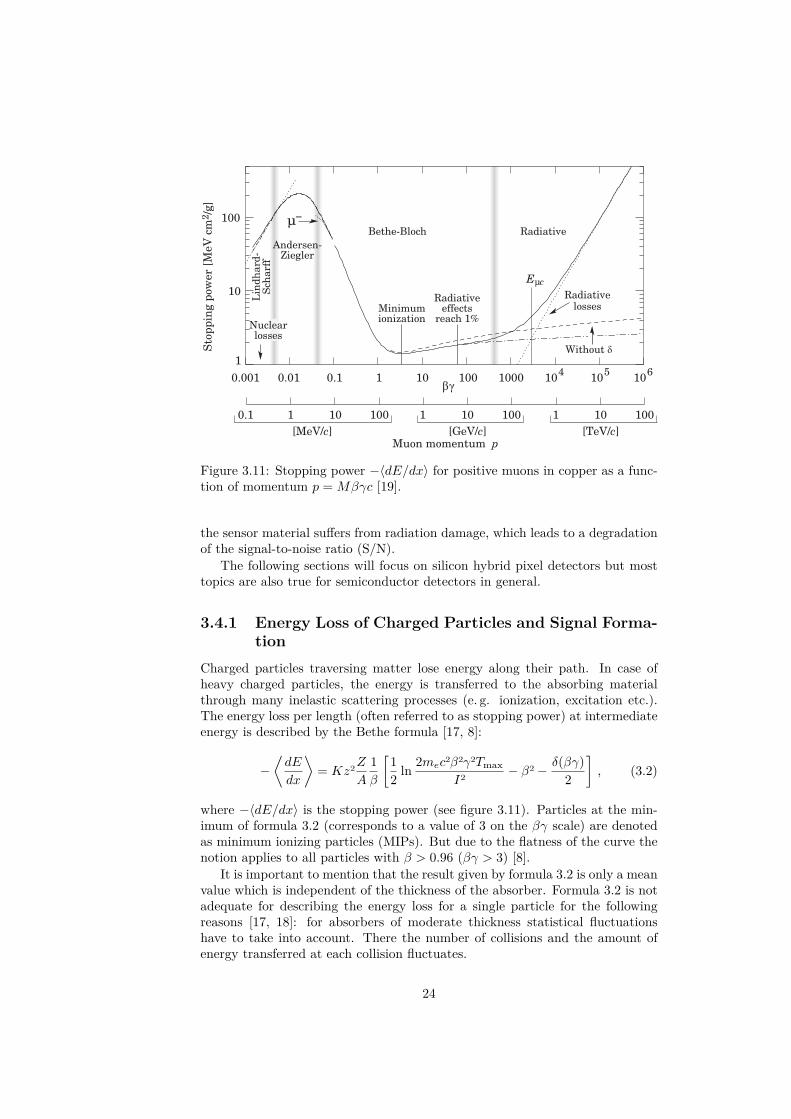
Figure 3.11: Stopping power ≠ÈdE/dxÍ for positive muons in copper as a func-tion of momentum p = M—“c [19].
the sensor material su�ers from radiation damage, which leads to a degradationof the signal-to-noise ratio (S/N).
The following sections will focus on silicon hybrid pixel detectors but mosttopics are also true for semiconductor detectors in general.
3.4.1 Energy Loss of Charged Particles and Signal Forma-tion
Charged particles traversing matter lose energy along their path. In case ofheavy charged particles, the energy is transferred to the absorbing materialthrough many inelastic scattering processes (e. g. ionization, excitation etc.).The energy loss per length (often referred to as stopping power) at intermediateenergy is described by the Bethe formula [17, 8]:
≠=
dE
dx
>= Kz�Z
A
1—
512 ln 2m
e
c�—�“�Tmax
I� ≠ —� ≠ ”(—“)2
6, (3.2)
where ≠ÈdE/dxÍ is the stopping power (see figure 3.11). Particles at the min-imum of formula 3.2 (corresponds to a value of 3 on the —“ scale) are denotedas minimum ionizing particles (MIPs). But due to the flatness of the curve thenotion applies to all particles with — > 0.96 (—“ > 3) [8].
It is important to mention that the result given by formula 3.2 is only a meanvalue which is independent of the thickness of the absorber. Formula 3.2 is notadequate for describing the energy loss for a single particle for the followingreasons [17, 18]: for absorbers of moderate thickness statistical fluctuationshave to take into account. There the number of collisions and the amount ofenergy transferred at each collision fluctuates.
24
100 200 300 400 500 6000.0
0.2
0.4
0.6
0.8
1.0
0.50 1.00 1.50 2.00 2.50
640 µm (149 mg/cm2)
320 µm (74.7 mg/cm2)
160 µm (37.4 mg/cm2)
80 µm (18.7 mg/cm2)
500 MeV pion in silicon
Mean energyloss rate
wf (!/x)
!/x (eV/µm)
!p/x
!/x (MeV g"1 cm2)
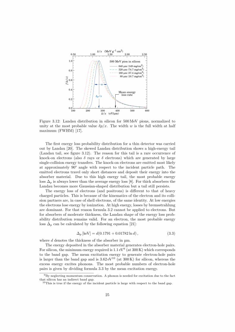
Figure 3.12: Landau distribution in silicon for 500 MeV pions, normalized tounity at the most probable value ”p/x. The width w is the full width at halfmaximum (FWHM) [17].
The first energy loss probability distribution for a thin detector was carriedout by Landau [20]. The skewed Landau distribution shows a high-energy tail(Landau tail, see figure 3.12). The reason for this tail is a rare occurrence ofknock-on electrons (also ” rays or ” electrons) which are generated by largesingle-collision energy transfers. The knock-on electrons are emitted most likelyat approximately 90° angle with respect to the incident particle path. Theemitted electrons travel only short distances and deposit their energy into theabsorber material. Due to this high energy tail, the most probable energyloss �
p
is always lower than the average energy loss [8]. For thick absorbers theLandau becomes more Gaussian-shaped distribution but a tail still persists.
The energy loss of electrons (and positrons) is di�erent to that of heavycharged particles. This is because of the kinematics of the electron and its colli-sion partners are, in case of shell electrons, of the same identity. At low energiesthe electrons lose energy by ionization. At high energy, losses by bremsstrahlungare dominant. For that reason formula 3.2 cannot be applied to electrons. Butfor absorbers of moderate thickness, the Landau shape of the energy loss prob-ability distribution remains valid. For an electron, the most probable energyloss �
p
can be calculated by the following equation [21]:
�p
[keV] = d(0.1791 + 0.01782 ln d) , (3.3)
where d denotes the thickness of the absorber in µm.The energy deposited in the absorber material generates electron-hole pairs.
For silicon, the minimum energy required is 1.1 eV9 (at 300 K) which correspondsto the band gap. The mean excitation energy to generate electron-hole pairsis larger than the band gap and is 3.62 eV10 (at 300 K) for silicon, whereas theexcess energy excites phonons. The most probable numbers of electron-holepairs is given by dividing formula 3.3 by the mean excitation energy.
9By neglecting momentum conservation. A phonon is needed for excitation due to the factthat silicon has an indirect band gap.
10This is true if the energy of the incident particle is large with respect to the band gap.
25
The free charge carriers need to be detected by the readout electronics. Themovement of the newly generated charge carriers induces a signal which canbe detected by the readout electronics. Because of an electric field, which isapplied to the detector by an external voltage supply, the electrons and holesstart drifting in opposite directions. Without field, the electrons and holeswould recombine after a short time without being recognized. The electronicproperties and conductivity of a semiconductor are decidedly determined by theconcentration of dopant atoms.
The equilibrium concentration of free charge carriers in a semiconductor canbe calculated by using the Fermi-Dirac statistics. The result of the calculationis independent of the doping concentration and is known as mass-action law[8]:
np = n
2
i
(3.4a)= N
C
N
V
e≠Eg/kT (3.4b)
In an intrinsic (undoped or pure) semiconductor in equilibrium the freecharge carriers are thermally generated. The number of free electrons is equalto the number of free holes and therefore the concentration n
i
of free charge car-riers can be calculated. The thermal excitation and recombination is supportedby imperfections within the crystal lattice and by impurities. It is extremelydi�cult to reach purity so that the lifetime of the free charge carriers is longenough so that an intrinsic semiconductor can be used for detecting ionizingradiation.
By adding a small fraction of dopant atoms new energy states are addedwithin the band gap. Donor states are close to the conduction band (e. g.0.054 eV for arsenic atoms in silicon) and acceptor states are close to the valenceband (e. g. 0.045 eV for boron atoms in silicon). At room temperature (k
B
T ¥0.025 eV) most of the donor and acceptor states are ionized. Material with moredonor atoms than acceptor atoms is called n-material and the majority chargecarriers are electrons according to the mass-action law. In p-type material themajority charge carriers are holes.
If p-doped and n-doped material forms a junction, free charge carriers willdi�use according to the concentration gradient of free electron and holes. Anelectrical field is generated by the di�usion and counter-acts the di�usion. Afraction of the free charge carriers drift back towards their majority carriesside. In equilibrium, the counter-acting voltage, which causes the drift, is calledbuilt-in voltage V
bi
and is in the order of 0.5 V. By applying a voltage (reversebias), which has the same direction as V
bi
, the recombination region can beextended even more. Around the junction, electrons and holes recombine. Therecombination region is free of charge carriers and has a high resistivity. Thisregion is called depletion zone (or space charge region). The width W of thedepletion zone is given by following equation [8]:
W =
Û2Á
0
Á
Si
e
31
N
A
+ 1N
D
4(V + V
bi
) . (3.5)
By assuming a p-n junction of a highly doped and lowly doped material (e. g.for an unirradiated ATLAS sensor is N
A
∫ N
D
), and by neglecting the built-involtage V
bi
one can derive the following relationship:
W =Ú
2Á
0
Á
Si
eN
D
V . (3.6)
26
In this case the depletion zone extends widely into the lowly doped region (inour example the n-type bulk). The voltage needed for full depletion is calleddepletion voltage V
depl
. Ideally, the depletion zone is extended over the completethickness of the sensor. But this is not always possible due to limitations on theheight of the supply voltage or early breakdown, to name a few. The size of thedepleted volume, and the geometry and strength of the electric field within thedepletion zone are important parameters which determines the e�ciency of thedetector. To receive maximum signal charge, a fully depleted sensor is essential.
Another important aspect is the detector capacitance which contributes tothe pre-amplifier input capacitance. The capacitance of the signal source shouldbe low in order to reduce the noise of the detector and to achieve a better overallS/N ratio [22, 18]. In case of planar sensor, the capacitance is influenced bythe size of the depleted region whose capacitance C can be approximated byfollowing formula [8]:
C(V ) =I
A
Á0ÁSiW (V )
V < V
depl
A
Á0ÁSid
V > V
depl
, (3.7)
where A is the size of the p-n junction and d the thickness of the sensor. Increas-ing the reverse bias voltage V leads to a lower sensor capacitance but increasesin revers the leakage current. The statistical fluctuations of the leakage cur-rent can be understood as noise current source feeding into the amplifier input(shot noise) [22]. However, for a pixel detector, the pixel to pixel capacitancedominates by far [18].
If an ionizing particle generates free charge carriers within the depletionzone, the charge carriers starts drifting along the electric field gradient to thecorresponding electrodes. The movement of the free charge carriers induce acurrent at the collecting electrodes and hence in the input of the readout am-plifier. The instantaneous current in the amplifier can be calculated by usingRamo’s Theorem [23]:
i = eEW
‹ , (3.8)
where v denotes the drift velocity of the charge carriers and is equal to µE.E
W
is the weighting field, which is given by ≠Ò„
W
, where „
W
is the weightingpotential. The weighting potential can be calculated by applying a unit potential(= 1) to the readout electrode and a zero potential to all the others. The injectedcharge is given by integrating over time:
Q =t2ˆ
t1
i(t)dt . (3.9)
In case of a pixel detector two conclusions can be drawn. They are denotedunder small pixel e�ect [8]:
• Most of the signal charge is induced by the charge carrier drift close tothe electrodes.
• Charge carriers drifting towards the backplane do not contribute signifi-cantly to the signal.
27
The first point particularly concerns irradiated sensors: the mobility µ and thelifetime ·
11 of free charge carriers is reduced and the result is a smaller signalcharge.
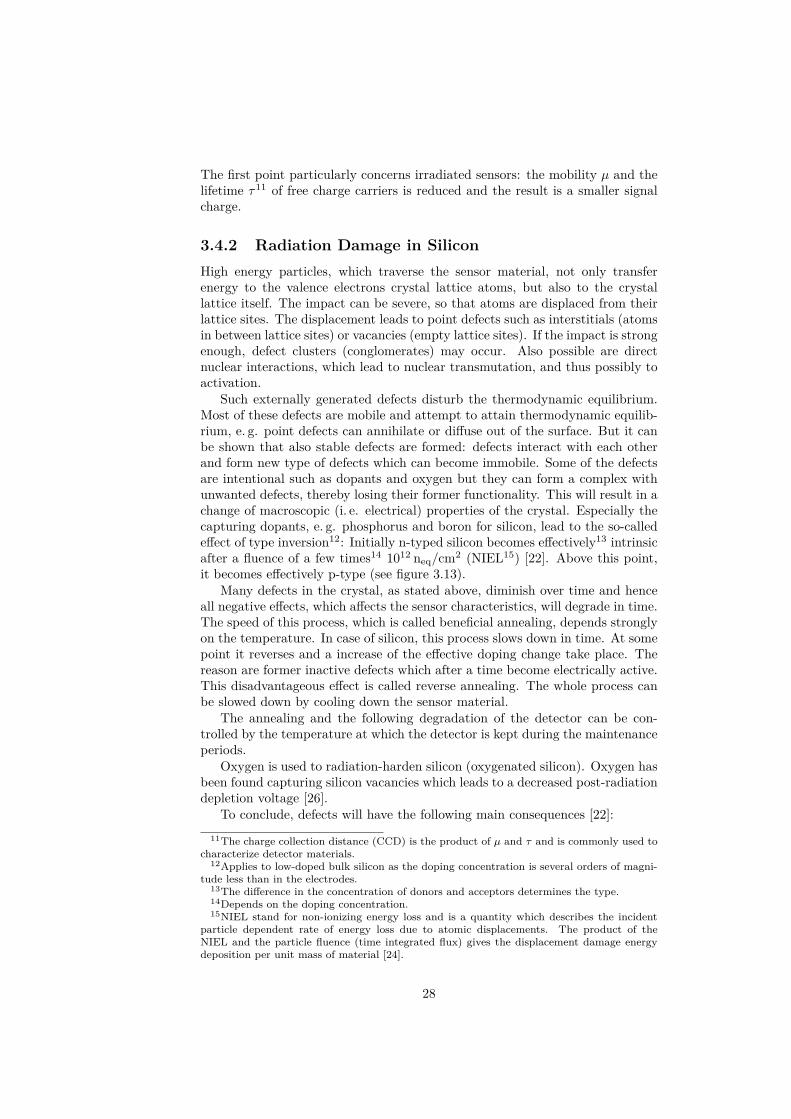
3.4.2 Radiation Damage in SiliconHigh energy particles, which traverse the sensor material, not only transferenergy to the valence electrons crystal lattice atoms, but also to the crystallattice itself. The impact can be severe, so that atoms are displaced from theirlattice sites. The displacement leads to point defects such as interstitials (atomsin between lattice sites) or vacancies (empty lattice sites). If the impact is strongenough, defect clusters (conglomerates) may occur. Also possible are directnuclear interactions, which lead to nuclear transmutation, and thus possibly toactivation.
Such externally generated defects disturb the thermodynamic equilibrium.Most of these defects are mobile and attempt to attain thermodynamic equilib-rium, e. g. point defects can annihilate or di�use out of the surface. But it canbe shown that also stable defects are formed: defects interact with each otherand form new type of defects which can become immobile. Some of the defectsare intentional such as dopants and oxygen but they can form a complex withunwanted defects, thereby losing their former functionality. This will result in achange of macroscopic (i. e. electrical) properties of the crystal. Especially thecapturing dopants, e. g. phosphorus and boron for silicon, lead to the so-callede�ect of type inversion12: Initially n-typed silicon becomes e�ectively13 intrinsicafter a fluence of a few times14 1012 n
eq
/cm2 (NIEL15) [22]. Above this point,it becomes e�ectively p-type (see figure 3.13).
Many defects in the crystal, as stated above, diminish over time and henceall negative e�ects, which a�ects the sensor characteristics, will degrade in time.The speed of this process, which is called beneficial annealing, depends stronglyon the temperature. In case of silicon, this process slows down in time. At somepoint it reverses and a increase of the e�ective doping change take place. Thereason are former inactive defects which after a time become electrically active.This disadvantageous e�ect is called reverse annealing. The whole process canbe slowed down by cooling down the sensor material.
The annealing and the following degradation of the detector can be con-trolled by the temperature at which the detector is kept during the maintenanceperiods.
Oxygen is used to radiation-harden silicon (oxygenated silicon). Oxygen hasbeen found capturing silicon vacancies which leads to a decreased post-radiationdepletion voltage [26].
To conclude, defects will have the following main consequences [22]:11The charge collection distance (CCD) is the product of µ and · and is commonly used to
characterize detector materials.12Applies to low-doped bulk silicon as the doping concentration is several orders of magni-
tude less than in the electrodes.13The di�erence in the concentration of donors and acceptors determines the type.14Depends on the doping concentration.15NIEL stand for non-ionizing energy loss and is a quantity which describes the incident
particle dependent rate of energy loss due to atomic displacements. The product of theNIEL and the particle fluence (time integrated flux) gives the displacement damage energydeposition per unit mass of material [24].
28
!eq [1012cm-2]
“p”-typen-type
type inversionU
dep [V
]
d = 300µm
"N
eff"
[1011
cm-3]
Figure 3.13: Absolute value of the e�ective doping concentration |Ne�
| depend-ing on the fluence �
eq
(neutrons, 1 MeV neutron equivalent) [25].
• They act as recombination–generation centers (recombination and genera-tion of electron-hole pairs); in the depletion zone this leads to an increasedreverse-bias (or leakage) current (shot noise, thermal runaway).
• They act as trapping centers; this leads to a reduced charge collectiondistance and hence smaller signal charge (loss of charge).
• They can change the charge density in the space-charge region; higherdepletion (or bias) voltage is needed or under depletion may occur.
The first two points have consequences for the S/N ratio. The increase ofthe reverse-bias current is the most noticeable change. The volume-generatedleakage current I
vol
increases linearly16 with the fluence „ [22]:
—I
vol
= –V „ , (3.10)
where V denotes the detector volume and – has to be determined. If the fluenceis scaled by the non-ionizing energy loss, then the increase of the leakage currentis independent of the particle type.
3.4.3 Sensor Types and TechnologiesFor a detector, an e�cient charge collection is necessary to meet the require-ments of space, time and energy resolution and overall e�ciency. All of thesepoints depend largely on the properties of the sensor. In addition the sensorhas to meet geometrical constraints on size and thickness while sustaining amassive amount of radiation damage. Concerning the IBL upgrade, there arethree sensor technologies which may fulfill the requirements [27]: planar, 3Dand diamond sensors. Each technology is demanding for di�erent operating andenvironmental variables such as reverse-bias voltage and operating temperature.The first two sensor concepts (see figure 3.14) will be explained in the following.
16Above type inversion, the rise is stronger (see figure 3.13).
29
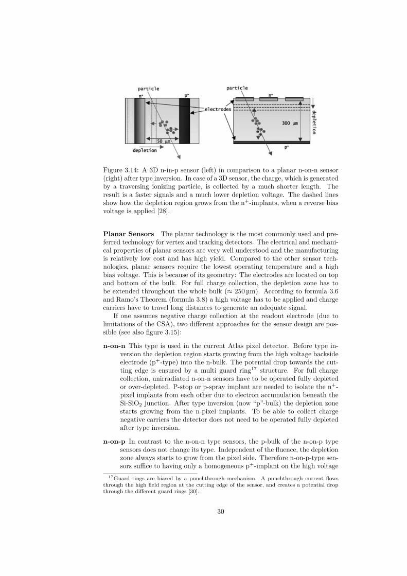
Figure 3.14: A 3D n-in-p sensor (left) in comparison to a planar n-on-n sensor(right) after type inversion. In case of a 3D sensor, the charge, which is generatedby a traversing ionizing particle, is collected by a much shorter length. Theresult is a faster signals and a much lower depletion voltage. The dashed linesshow how the depletion region grows from the n+-implants, when a reverse biasvoltage is applied [28].
Planar Sensors The planar technology is the most commonly used and pre-ferred technology for vertex and tracking detectors. The electrical and mechani-cal properties of planar sensors are very well understood and the manufacturingis relatively low cost and has high yield. Compared to the other sensor tech-nologies, planar sensors require the lowest operating temperature and a highbias voltage. This is because of its geometry: The electrodes are located on topand bottom of the bulk. For full charge collection, the depletion zone has tobe extended throughout the whole bulk (¥ 250 µm). According to formula 3.6and Ramo’s Theorem (formula 3.8) a high voltage has to be applied and chargecarriers have to travel long distances to generate an adequate signal.
If one assumes negative charge collection at the readout electrode (due tolimitations of the CSA), two di�erent approaches for the sensor design are pos-sible (see also figure 3.15):
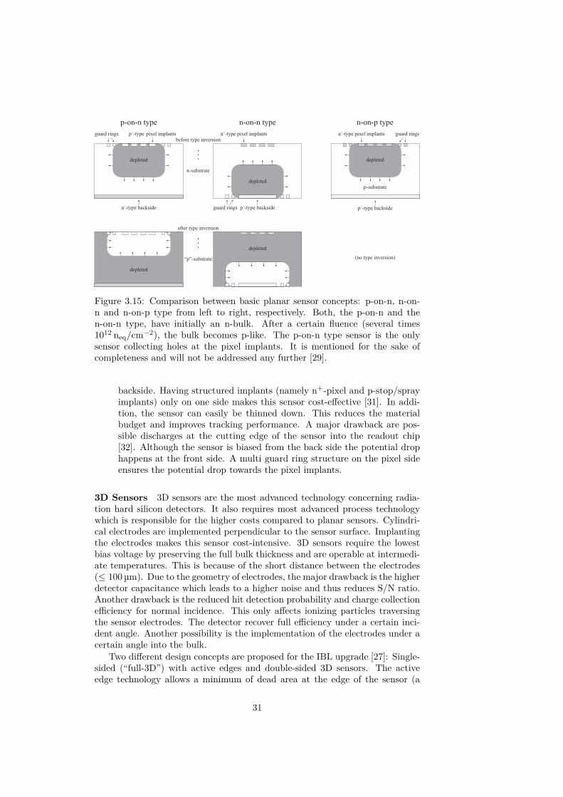
n-on-n This type is used in the current Atlas pixel detector. Before type in-version the depletion region starts growing from the high voltage backsideelectrode (p+-type) into the n-bulk. The potential drop towards the cut-ting edge is ensured by a multi guard ring17 structure. For full chargecollection, unirradiated n-on-n sensors have to be operated fully depletedor over-depleted. P-stop or p-spray implant are needed to isolate the n+-pixel implants from each other due to electron accumulation beneath theSi-SiO
2
junction. After type inversion (now “p”-bulk) the depletion zonestarts growing from the n-pixel implants. To be able to collect chargenegative carriers the detector does not need to be operated fully depletedafter type inversion.
n-on-p In contrast to the n-on-n type sensors, the p-bulk of the n-on-p typesensors does not change its type. Independent of the fluence, the depletionzone always starts to grow from the pixel side. Therefore n-on-p-type sen-sors su�ce to having only a homogeneous p+-implant on the high voltage
17Guard rings are biased by a punchthrough mechanism. A punchthrough current flowsthrough the high field region at the cutting edge of the sensor, and creates a potential dropthrough the di�erent guard rings [30].
30
depleted
depleted
depleted
depleted
depleted
“p”-substrate
after type inversion
n-substrate
guard rings
n-on-n type
guard rings
p-on-n type
n+-type pixel implants
n-on-p type
p-substrate
guard ringsn+-type pixel implants
n+-type backside p+-type backside p+-type backside
(no type inversion)
p+-type pixel implantsbefore type inversion
Figure 3.15: Comparison between basic planar sensor concepts: p-on-n, n-on-n and n-on-p type from left to right, respectively. Both, the p-on-n and then-on-n type, have initially an n-bulk. After a certain fluence (several times1012 n
eq
/cm≠2), the bulk becomes p-like. The p-on-n type sensor is the onlysensor collecting holes at the pixel implants. It is mentioned for the sake ofcompleteness and will not be addressed any further [29].
backside. Having structured implants (namely n+-pixel and p-stop/sprayimplants) only on one side makes this sensor cost-e�ective [31]. In addi-tion, the sensor can easily be thinned down. This reduces the materialbudget and improves tracking performance. A major drawback are pos-sible discharges at the cutting edge of the sensor into the readout chip[32]. Although the sensor is biased from the back side the potential drophappens at the front side. A multi guard ring structure on the pixel sideensures the potential drop towards the pixel implants.
3D Sensors 3D sensors are the most advanced technology concerning radia-tion hard silicon detectors. It also requires most advanced process technologywhich is responsible for the higher costs compared to planar sensors. Cylindri-cal electrodes are implemented perpendicular to the sensor surface. Implantingthe electrodes makes this sensor cost-intensive. 3D sensors require the lowestbias voltage by preserving the full bulk thickness and are operable at intermedi-ate temperatures. This is because of the short distance between the electrodes(Æ 100 µm). Due to the geometry of electrodes, the major drawback is the higherdetector capacitance which leads to a higher noise and thus reduces S/N ratio.Another drawback is the reduced hit detection probability and charge collectione�ciency for normal incidence. This only a�ects ionizing particles traversingthe sensor electrodes. The detector recover full e�ciency under a certain inci-dent angle. Another possibility is the implementation of the electrodes under acertain angle into the bulk.
Two di�erent design concepts are proposed for the IBL upgrade [27]: Single-sided (“full-3D”) with active edges and double-sided 3D sensors. The activeedge technology allows a minimum of dead area at the edge of the sensor (a
31

few µm compared to a few 100 µm). Active edges becomes an important featureregarding IBL since overlapping (shingling) of modules in direction of the beampipe is not possible.
32
Chapter 4
The USBpix Test System
4.1 IntroductionUSBpix was developed as a small and light weighting test system for ATLASFE-I3 pixel readout chips. As successor to TurboDAQ, which is rather bigin size and consists of many expensive hardware components, it provides thefunctionality which is needed for a full characterization of pixel sensors attachedto the FE-I3 pixel readout chip.
The development of the USBpix readout system started in the late 2008.The hardware design and basic software parts (USB driver, microcontrollercode, hardware interface libraries, and basic FPGA code) were developed atSiLAB1[33, 34]. Other parts of the software (STcontrol and PixLib) were con-tributed by the ATLAS Pixel Collaboration and were adapted to the USBpixtest system with support of University of Göttingen2.
A main part of this diploma thesis covers the code maintenance and fur-ther development of the USBpix test system for the FE-I3 readout chip. In thebeginning of this work, source code refactoring was the main task to ensure ex-tensibility and maintainability of the test system. During this work many partsof the source code were rewritten and new functionality was added. Changeswere made to all system levels, i.e. driver, microcontroller code, libraries, userinterface and in particular to the FPGA code. Continuous testing and the char-acterization of sensors (see section 6) during the development cycles helped toimprove the overall quality of the software.
Furthermore, USBpix is capable to fulfill the needs for an ATLAS FE-I4 testsystem, of which development started in the late 2009. The FE-I3 test system’ssource code was ported to support the future ATLAS FE-I4 readout chip whichis foreseen for a future IBL upgrade of the ATLAS pixel detector.
4.2 RequirementsThe USBpix test system main purpose is the characterization of new genera-tion of sensor material intended for being used for IBL and HL-LHC detector
1Silizium Labor der Univerität Bonn, Nussallee 12, D-53115 Bonn, Germany.2Georg-August-Universität Göttingen, II. Physikalisches Institut, Friedrich-Hund-Platz 1,
D-37077 Göttingen, Germany.
33
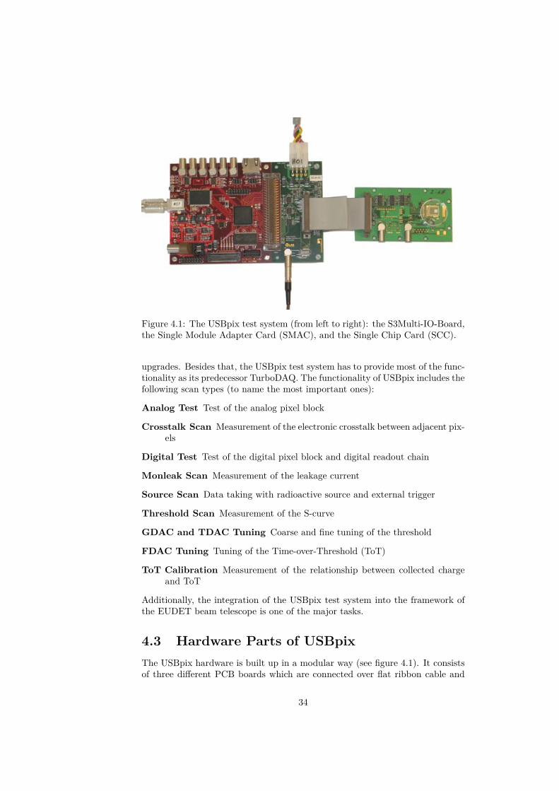
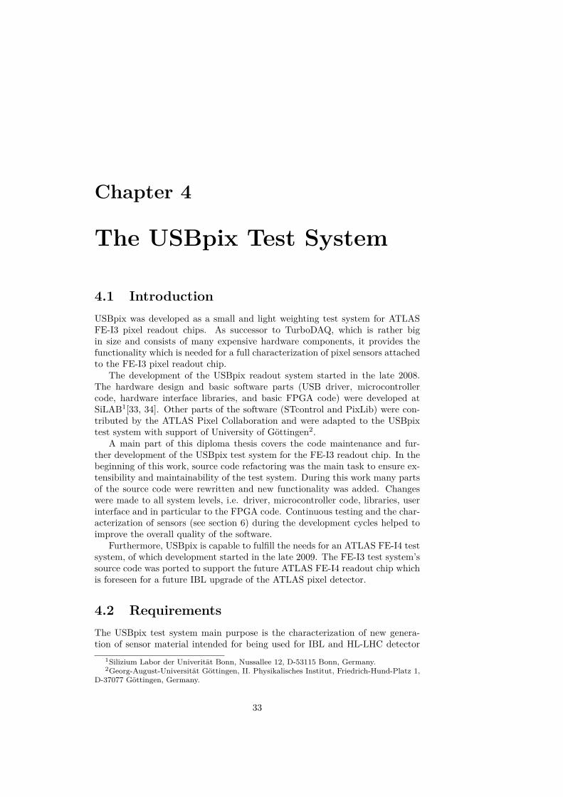
Figure 4.1: The USBpix test system (from left to right): the S3Multi-IO-Board,the Single Module Adapter Card (SMAC), and the Single Chip Card (SCC).
upgrades. Besides that, the USBpix test system has to provide most of the func-tionality as its predecessor TurboDAQ. The functionality of USBpix includes thefollowing scan types (to name the most important ones):
Analog Test Test of the analog pixel block
Crosstalk Scan Measurement of the electronic crosstalk between adjacent pix-els
Digital Test Test of the digital pixel block and digital readout chain
Monleak Scan Measurement of the leakage current
Source Scan Data taking with radioactive source and external trigger
Threshold Scan Measurement of the S-curve
GDAC and TDAC Tuning Coarse and fine tuning of the threshold
FDAC Tuning Tuning of the Time-over-Threshold (ToT)
ToT Calibration Measurement of the relationship between collected chargeand ToT
Additionally, the integration of the USBpix test system into the framework ofthe EUDET beam telescope is one of the major tasks.
4.3 Hardware Parts of USBpixThe USBpix hardware is built up in a modular way (see figure 4.1). It consistsof three di�erent PCB boards which are connected over flat ribbon cable and
34
(a) (b)
Figure 4.2: (a) Block diagram of the S3Multi-IO-Board. (b) Picture of theS3Multi-IO-Board [35].
on-board connectors. The entire hardware of the test system is connected via aUSB 2.0 Hi-Speed interface (480 Mbps raw data speed) to a host computer (orDAQ computer) which is running the control software (STcontrol).
4.3.1 S3Multi-IO-BoardThe S3Multi-IO-Board is a multi-purpose I/O board (Rev. 1.03, see figure 4.2).It is the central control unit of the test system containing all of the pro-grammable hardware parts. The communication between the host computerand the S3Multi-IO-Board is implemented in an 8051-based USB-capable micro-controller (Cypress CY7C68013A). The 8051-microcontroller steers the commu-nication between hardware parts on the S3Multi-IO-Board (FPGA, EEPROM,programmable clock generator, ADC; for more details see following sections)and the software running on the host computer. To set the programmable clockgenerator (Cypress CY22150FZXI) or to read out the analog-to-digital con-verters (Maxim MAX1238, located on the Adapter Card) the microcontrolleruses a 2-wire I�C serial interface. The EEPROM (Microchip 24LC128), whichcontains the firmware of the microcontroller, is serially connected to the 8051-microcontroller. Registers and Block RAM inside the FPGA (Xilinx Spartan-3XC3S1000-FGG320) can be accessed by using the Slow Interface. The SlowInterface3 is a 8-bit wide parallel data bus with a 48 MHz clock (UCLK, in-ternal clock of the microcontroller). The address space is 16-bit wide. Themicrocontroller and the FPGA have access to 16 Mbit asynchronous SRAM.The SRAM (Cypress CY7C1061AV33) is connected to a 16-bit wide data bus4.The clock speed depends on whether the microcontroller or the FPGA is ac-cessing the SRAM and is 48 MHz or 40 MHz, respectively. The memory can
3The name derives from the fact that the internal clock was initially running on 24 MHz.The speed of the internal clock was changed during this thesis.
4A 16-bit wide parallel interface is available in hardware but not implemented in software.Currently, only a 8-bit wide data bus is used.
35
be accessed through a 20-bit wide address bus. The overall maximum read-out speed reaches 1
/4 of the raw data speed of the USB 2.0 Hi-Speed interface(approximately 15 MB/s).
Various input/output (I/O) connectors can be accessed by the FPGA. Themain I/O connector (100-pin connector) is placed on the edge of the S3Multi-IO-Board and can hold di�erent types of adapter cards. In addition, thereare various other multi-purpose I/O ports available. Six LEMO connectors, an8P8C5 jack, a 100-pin Samtec connector and a 16 pin header are placed on theS3Multi-IO-Board.
4.3.2 Single Module Adapter Card
The Single Module Adapter Card (SMAC, Rev. 1.2) holds low-voltage di�er-ential signaling (LVDS) transceiver to enable high-speed data transmission overstandard flat ribbon cable. The flat ribbon cable connects the SMAC to theSingle Chip Card (see next section). Additionally, analog voltage (AVDD), dig-ital voltage (DVDD) and low voltage (LVDD), which are needed for the SingleChip Card (see section 4.3.3), are transmitted over the flat ribbon cable. Thesupply voltages are received from external power supplies which are connectedto the 8-pin Molex power connector. The SMAC also holds an analog-to-digitalconverter (ADC) which is connected to the microcontroller over the I�C bus.The ADC reads out AVDD and DVDD, and a negative temperature coe�cient(NTC) thermistor which can be soldered to the Single Chip Card.
4.3.3 Single Chip Card
The Single Chip Card (SCC) holds the FE-I3 chip which receives AVDD andDVDD from the SMAC. LVDS transceivers are placed on the SCC to convertincoming LVDS signals to single-ended CMOS and vice versa. The transceiverscan either be powered by using LVDD (2.8 V) from the SMAC or externally byconnecting a power supply to a LEMO connector. Another LEMO connectorcan be connected to a high voltage power supply and receives bias voltage forbiasing the sensor. Two more LEMO connectors are available which providesaccess to the MonAmp and VCal pad on the FE-I3 chip.
Several test pads are available for testing and measuring signal integrity ofthe FE-I3 readout chip. Some of them are needed during chip/sensor charac-terization (see section 5.4).
4.4 Software Framework of USBpixThe software framework of USBpix has a multi-layer structure which reflectsthe hardware structure of the test system. It encapsulates functionality withinuseable objects which creates function modules. In the following sections, acloser look will be given on the USBpix framework. The focus is on changeswhich have made during this thesis.
58P8C jacks are often referred to as “RJ-45” jacks.
36
4.4.1 USB DriverThe USB driver controls the data transfer between the host computer (USBmaster) and the peripheral device (USB slave), which is built into the USB-capable 8051-microcontroller. A driver for Microsoft Windows6 is available aswell as a Linux kernel mode driver.
During this thesis it turned out that the Linux driver has compatibilityissues with recent Linux kernels (2.6.24 and upwards). E�orts were undertakento solve these issues but without success.
A possible solution for that issue is to use the open source libusb7 driver forboth Microsoft Windows and Linux-based systems.
4.4.2 SiUSBLib LibraryThe SiUSBLib library is a collection of classes and functions providing rudi-mentary access to the USBpix hardware. SiUSBLib is implemented as a dy-namically linked library8 (DLL), namely SiUSBLib.dll. To give access to theUSBpix hardware other objects and libraries can be built against9 SiUSBLiblibrary.
The functionality of SiUSBLib library is closely related to the USBpix hard-ware. It provides functionality which gives access to the hardware such as pro-gramming the microcontroller and FPGA, flashing the EEPROM, and writingand reading SRAM and registers.
Under Microsoft Windows and Linux-based systems the USB device handlingis controlled by the SiUSBLib library. Due to historical reasons the maximumnumber of USBpix boards, which can be attached to a single host computer, islimited to 8 peripheral devices (mainly due to limitations of the USB driver).During this thesis it shows up that this limitation leads to erroneous multi-device handling so that the host computer can securely handle only one USBdevice at the same time. Changes in the USB driver and the SiUSBLib libraryare needed to overcome this limitation.
Another possible solution to overcome this limitation, it is suitable to usethe libusb driver (see section 4.4.1). In either case, the SiUSBLib library needsto be adapted.
During this thesis only slight changes were made to the SiUSBLib library.Only the ReadInterrupt(...) and WriteInterrupt(...) functions werechanged to support new functionality in the USBpixdll library (see section 4.4.3),and microcontroller firmware (see section 4.5).
4.4.3 USBpixdll LibraryThe USBpixdll library consists of classes providing access to the functionalitywhich is built into the FPGA and microcontroller. To get access to the USBpix
6The USB driver supports Microsoft Windows XP/Vista/7 (32-bit).7Libusb is a library which gives user level applications uniform access to USB devices across
many di�erent operating systems. Libusb is an open source project licensed under the GNULesser General Public License version 2.1 (LGPLv2.1). http://www.libusb.org
8A dynamic link library is executable code which is loaded and linked during load time orruntime. Only a minimum amount of work is done during link time.
9This process is also called linking. After compilation, the linker links all of the specifiedobject and library files to create executable files.
37
hardware, USBpixdll library uses functionality provided by the SiUSBLib li-brary (USBpixdll library is built against the SiUSBLib library). USBpixdlllibrary is implemented as a DLL (usbpixdll.dll).
During this thesis, most parts of USBpixdll library were rewritten. In thefollowing paragraphs a closer look will be given to particular changes to theclasses.
The ConfigRegister class was completely rewritten and new functionality wasimplemented. This class provides access to the register inside the FPGA (seesection 4.6) as well as to the SRAM on the S3Multi-IO-Board. It makes func-tionality available, which is implemented in the FPGA, to other classes or appli-cations, but protect it against improper operation. This class is also responsiblefor data related tasks. It reads out and processes the data produced duringevery scan, so that higher-level applications have easy access to histogrammeddata. Most of the changes were made due to the implementation of the Source-Scan (see section 5.8). Functions for controlling the Source-Scan and readingout the status of the Source-Scan were implemented. To give existing dataanalysis software access to the raw data, which is generated during the SourceScan (see section 5.8), it is possible to write TurboDAQ-compatible output files.Additionally several histogram functions were added to ConfigRegister. Theywere used to introduce new types of histograms to STcontrol/PixLib. Amongthese histogram functions two di�erent cluster algorithms and a seed findingalgorithm were implemented (see section 5.9.2).
The ConfigFEMemory class provides functionality to configure the FE-I3readout chip. It has access to the Block RAM10 to store and modify FE-I3 globaland pixel register data. During this thesis mainly source code maintenance wasperformed.
4.4.4 USBpixController ClassThe USBpixController class is the interface class between the STcontrol/PixLibDAQ and the classes belonging to the USBpixdll library (see previous section).The goal of the USBpixController class is to hide implementation details ofUSBpix from STcontrol/PixLib DAQ.
During this thesis many changes were made to the USBpixController class,in particular code maintenance and implementation of new functionality (e.g.Source Scan), which have implemented into USBpix.
4.5 Microcontroller FirmwareMost parts of the microcontroller source code are provided “as is”. The corefunctionality (access to the hardware components on the S3Multi-IO-Board asdescribed in section 4.3.1) relies on functionality implemented in the SiUSBLiblibrary (see section 4.4.2).
Functionality was implemented to run a full scan (e. g. Threshold Scan, ToTScan) on the 8051-microcontroller without any interaction between the hostcomputer and the microcontroller [34]. For that purpose, the microcontrollerhas access to the registers and Block RAM inside the FPGA to control theFSMs and to change the global and pixel register data of the FE-I3. During
10Block RAM is a dedicated dual-port memory placed on the FPGA.
38
the scan, histogrammed data is stored in the SRAM for later readout (for moredetails, see following section).
During this thesis, parts of microcontroller source code, in particular thoseconcerning the automatic scans loop, were rewritten to ensure stability and dataintegrity. The ability to apply all possible FE-I3 masks was added. In additionto that, the mask shifting problem with two applied masks (e. g. SEL-ENA, SEL-PRE) was solved. During this thesis it turned out that simultaneous shifting oftwo pixel masks at the same time results in “missing hits”. It turned out thatthis only a�ects the first charge injection11 immediately after the mask shift.This means, that the strobe signal was applied to a pixel but no hit was seen. Tocome over this problem, a “fake injection”12 is applied to every pixel before theregular injection starts. In other words, after every mask shifting an additionalcharge injection is applied (strobe signal) but the data received from the FE-I3associated with this injection is not saved. The reason for this behavior is notunderstood but is most likely a feature of the FE-I3 readout chip. This behaviorwill not a�ect the operation of the test systems, nor regular detector operation.Similar problems while shifting of three masks (SEL-ENA-PRE) at the sametime is also not understood and left unresolved.
During the work on the microcontroller firmware, a severe bug, which resultsin a measured threshold discrepancy between TurboDAQ and USBpix, was fixed.The threshold discrepancy between TurboDAQ and USBpix was observed forthe first time in [34] and then verified in [36]. The threshold discrepancy wasdue to a programming error in the microcontroller source code which put thehistogrammed data into the wrong memory location. This was fixed as of release1.4 of USBpix. For a threshold comparison between USBpix and TurboDAQsee figure 4.3.
4.6 FPGA FirmwareMany a�ords were undertaken to redesign the source code of the FPGA firmware.This was done in a two stage process. The first step was refactoring of the sourcecode. During this process the existing source code was replaced without modify-ing the external functionality and behavior. In a second step, new functionalitywas added and the source code was further developed. The next paragraphswill highlight the functionality and the changes made during this work.
To define the behavior of the FPGA, the Verilog13 programming languagewas used. Verilog is hardware description language (HDL) which is most com-monly used to describe and simulate digital designs. The syntax of Verilog issimilar to C programming language (e. g. bitwise operators, statements). In ad-dition to being able to process sequential/synchronous logic, which is supportedby most of today’s programming languages, Verilog also incorporates syntax todescribe combinatorial/asynchronous logic.
Figure 4.4 gives an overview of the modular structure of the USBpix HDLdesign. A Verilog design consists of a hierarchy of modules, starting with the
11On the rising edge of the strobe signal negative charge is injected into the preamplifier(see section 5.4).
12The FPGA has to be set to “fake injection mode” (see section 4.6). Set to this mode, theFPGA receives raw data but doesn’t save histogrammed data to the SRAM.
13IEEE 1364-2001, known as Verilog-2001.
39
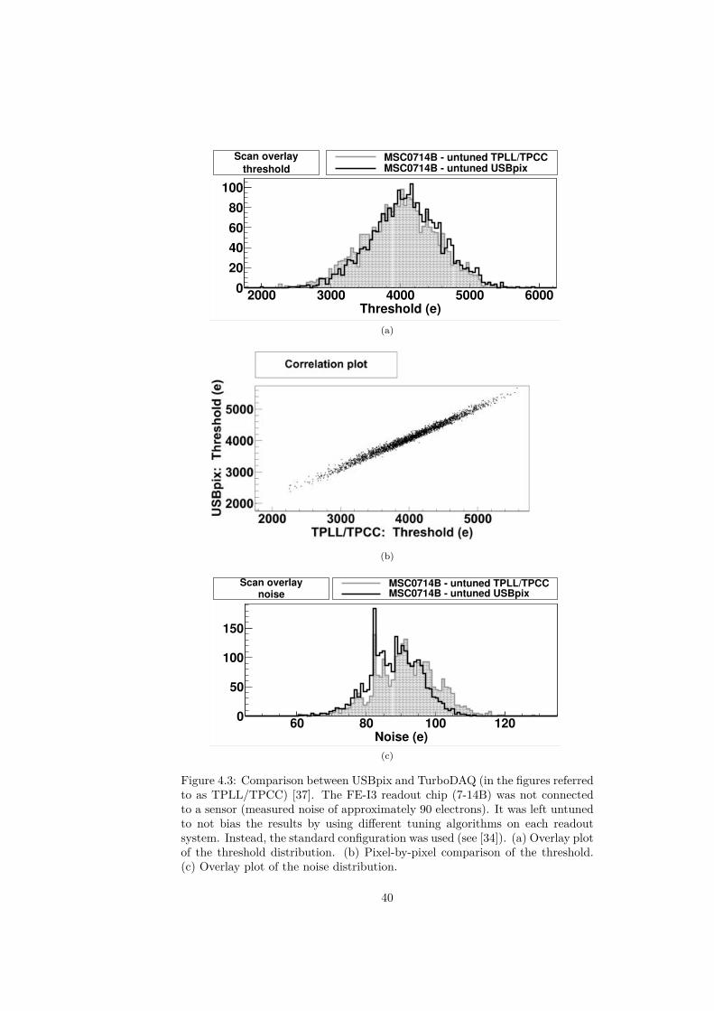
Threshold (e)2000 3000 4000 5000 6000
0
20
40
60
80
100
MSC0714B - untuned TPLL/TPCCMSC0714B - untuned USBpix
Scan overlaythreshold
(a)
(b)
Noise (e)60 80 100 120
0
50
100
150
MSC0714B - untuned TPLL/TPCCMSC0714B - untuned USBpix
Scan overlaynoise
(c)
Figure 4.3: Comparison between USBpix and TurboDAQ (in the figures referredto as TPLL/TPCC) [37]. The FE-I3 readout chip (7-14B) was not connectedto a sensor (measured noise of approximately 90 electrons). It was left untunedto not bias the results by using di�erent tuning algorithms on each readoutsystem. Instead, the standard configuration was used (see [34]). (a) Overlay plotof the threshold distribution. (b) Pixel-by-pixel comparison of the threshold.(c) Overlay plot of the noise distribution.
40
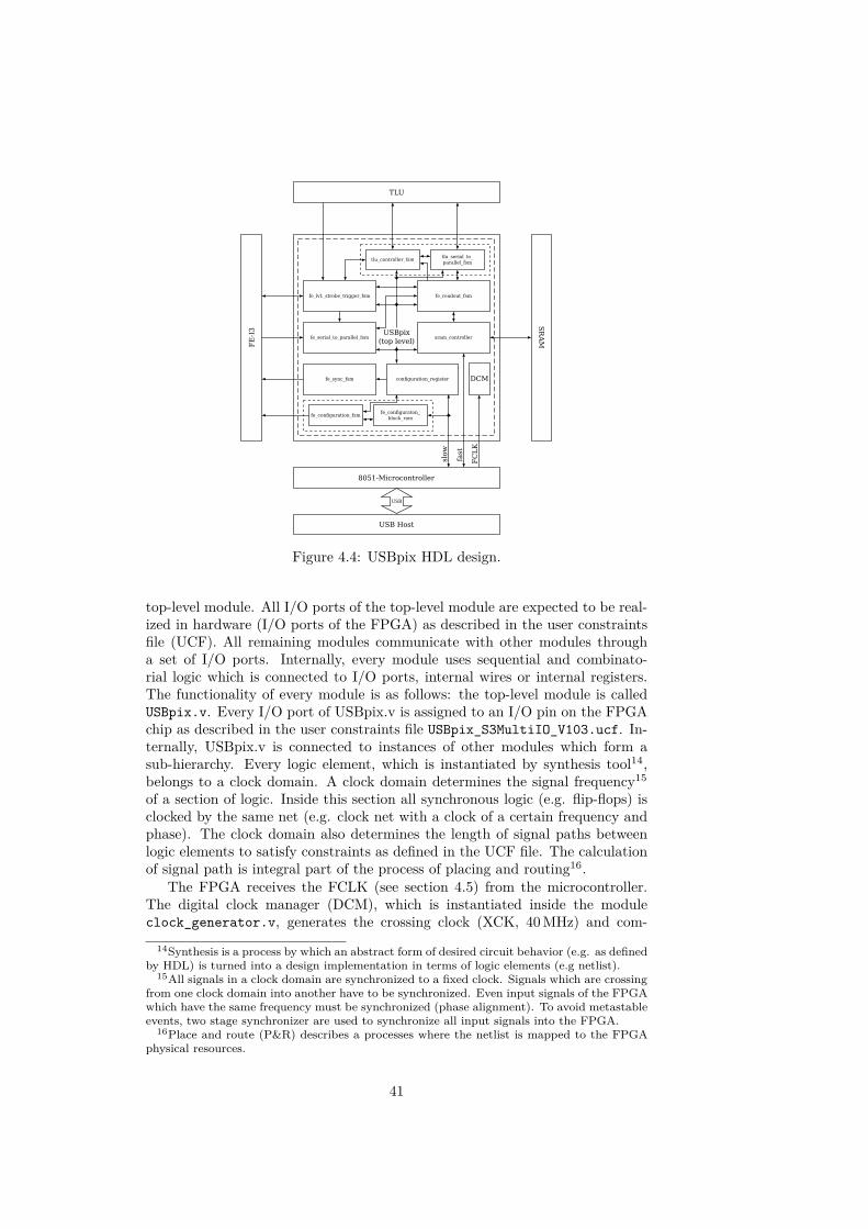
Figure 4.4: USBpix HDL design.
top-level module. All I/O ports of the top-level module are expected to be real-ized in hardware (I/O ports of the FPGA) as described in the user constraintsfile (UCF). All remaining modules communicate with other modules througha set of I/O ports. Internally, every module uses sequential and combinato-rial logic which is connected to I/O ports, internal wires or internal registers.The functionality of every module is as follows: the top-level module is calledUSBpix.v. Every I/O port of USBpix.v is assigned to an I/O pin on the FPGAchip as described in the user constraints file USBpix_S3MultiIO_V103.ucf. In-ternally, USBpix.v is connected to instances of other modules which form asub-hierarchy. Every logic element, which is instantiated by synthesis tool14,belongs to a clock domain. A clock domain determines the signal frequency15
of a section of logic. Inside this section all synchronous logic (e.g. flip-flops) isclocked by the same net (e.g. clock net with a clock of a certain frequency andphase). The clock domain also determines the length of signal paths betweenlogic elements to satisfy constraints as defined in the UCF file. The calculationof signal path is integral part of the process of placing and routing16.
The FPGA receives the FCLK (see section 4.5) from the microcontroller.The digital clock manager (DCM), which is instantiated inside the moduleclock_generator.v, generates the crossing clock (XCK, 40 MHz) and com-
14Synthesis is a process by which an abstract form of desired circuit behavior (e.g. as definedby HDL) is turned into a design implementation in terms of logic elements (e.g netlist).
15All signals in a clock domain are synchronized to a fixed clock. Signals which are crossingfrom one clock domain into another have to be synchronized. Even input signals of the FPGAwhich have the same frequency must be synchronized (phase alignment). To avoid metastableevents, two stage synchronizer are used to synchronize all input signals into the FPGA.
16Place and route (P&R) describes a processes where the netlist is mapped to the FPGAphysical resources.
41
mand clock (CCK, 4 MHz17) by multiplying or dividing the incoming FCLK.The FCLK is used in the sram_controller.v module for reading out the SRAM(fast interface). Additionally, the FCLK is used for writing data, which is re-ceived from the microcontroller via the slow interface, to the registers inside theFPGA. Those registers are placed in the configuration_register.v module.
The XCK and the CCK are mainly used to drive the flip-flops which areplaced inside the FPGA. Both clocks are getting forwarded to an attached FE-I3 readout chip using a double-data rate flip-flop (OFDDRRSE) to deskew datato clock phase alignment.
The behavior of combinatorial logic and finite state machines18 (FSM), whichare instantiated inside the FPGA, can be controlled by setting registers val-ues. The corresponding registers placed inside the configuration_register.vmodule. The FSM coding style is using the three always block coding style(two sequential always blocks and one combinatorial always block) with regis-tered outputs. This coding style was chosen because it is easily modifiable andextendable and is readable by every HDL design tool (e. g. Aldec Active-HDL,Mentor Graphics Precision Synthesis). Following FSM were developed duringthis thesis:
fe_lv1_strobe_trigger_fsm.v This module contains a FSM, which controlsthe length, delay and the number of repetitions of the strobe and LV1signal, which are sent to the FE-I3. In source scan mode, this FSM alsoreceives the external trigger signal. The external trigger signal causesthe generation of the LV1 trigger signal. This process is repeated untilthe desired number of triggers signals, hit words or EoE words is received.Two trigger input ports are available on the USBpix board: A LEMO RX0jack19 and the RJ45 jack (intended to be used by the trigger logic unit(TLU), see next section for more details). Di�erent sources of a triggersignal can be used to trigger the readout, e. g. the FE-I3 hitbus signal(self-triggering20), an amplifier/discriminator board or the TLU.
fe_serial_to_parallel_sr_fsm.v This module contains a 26-bit shift regis-ter which is receiving the serial raw data from the FE-I3 readout chip.The FSM reads out the shift register data and makes it available to otherFSMs on a 26-bit wide internal bus. The FSM also checks the receiveddata: it recognizes whether the data is an EoE word or hit word andchecks for errors and invalid data and sets an appropriate flag inside thetrigger word (see table 4.1).
17The CCK operates at 5 MHz. In order to reuse the CCK for reading out the Trigger LogicUnit (see section 4.7) the frequency was lowered to 4 MHz. This saves the use of another DCMand low skew clock net inside the FPGA. The change of the frequency of the configurationclock has no influence on the behaviour of the FE-I3 readout chip.
18A finite state machine consists of sequential and combinatorial logic. It is a model ofbehavior composed of a finite number of states. The output values of a FSM are determinedby its current state and by the input values (Mealy machine). The transition between thosestates depends on the current state and is also influenced by the input values.
19LVTTL/LVCMOS, unipolar, 0... + 3.3 V.20The LEMO TX2 jack has to be connected to the LEMO RX0 jack. The MonHit MUX
has to be set up so that the hitbus signal is available on the MonHit output pin of the FE-I3(global register [23:26]). This self-trigger mode should not be confused with the internal self-trigger as described in [12], whereas in both cases the hitbus signal is used to generate theLV1 trigger.
42
fe_readout_fsm.v This FSM is reading out the parallel data on the 26-bitwide internal bus and controls the data writing to the SRAM. Dependingon the readout mode (“fake injection mode”, “ToT mode”, “calibrationmode”, “source scan mode”) di�erent data is written to the SRAM. The“fake injection mode”, “ToT mode” and “calibration mode” are set by themicrocontroller depending on the scan type (e. g. ToT Scan, ThresholdScan). If the FSM is set to “fake injection mode”, no data is written tothe SRAM (see section 4.5). If set to “ToT mode”, only histogrammedToT data is written to the SRAM to save memory. The data is storedat predetermined addresses within the SRAM, depending on the pixeladdress (column/row) and the scan loop number. The same is true forthe “calibration mode”, but in this mode only hit information is saved (hitword counter). In source scan mode all hit words and EoE words receivedfrom the readout chip are written to the SRAM. Also a 32-bit trigger wordis stored to the SRAM to identify the BCID windows21. The trigger wordis stored behind the last received EoE word which belongs to a BCIDwindow. The trigger word consists of a 1-bit header and 31-bit triggerdata. Depending on the trigger mode, the trigger number is generatedinternally (trigger counter, only in no-handshake and simple handshakemode) or is received from the TLU (TLU trigger number, only in triggerdata handshake mode). If enabled, additional status data can be added toevery trigger word by means of cutting o� 8 most significant bits (MSB)of the trigger number. The status data includes 6 error bits and 2 bits forthe trigger mode (see table 4.1). The status data can be used by externalanalysis software to detect if the BCID window is incomplete or defect.
fe_configuration_fsm.v This FSM writes to the configuration registers ofthe FE-I3 readout chip. It controls the CCK and the LD signal and hasaccess to two dual-port Block RAMs (RAMB16_S1_S9), which containthe configuration data. Two sets of each global register data (231 bit)and pixel register data (2880 bit) can be stored at the same time in-side the Block RAMs. One Block RAM holds the configuration data forwriting to the FE-I3, and the other one holds configuration data thatis read back from the FE-I3 readout chip. This allows the verificationof the configuration data which is stored inside the FE-I3 registers. TheBlock RAMs are instantiated inside the fe_configuration_block_ram.vmodule. Both modules, in turn, are instantiated inside the higher-levelfe_configuration.v module.
The next section will cover the EUDET telescope integration and will highlightfunctionality implemented in the FPGA design.
21A BCID window is a series of EoE words and hit words which belong to a sequence ofconsecutive LV1 triggers (maximum of 16 consecutive LV1 trigger à 25 ns). The number ofEoE words corresponds to the total length of the LV1 trigger in units of bunch crossings (abunch crossing is equivalent to 25 ns).
43
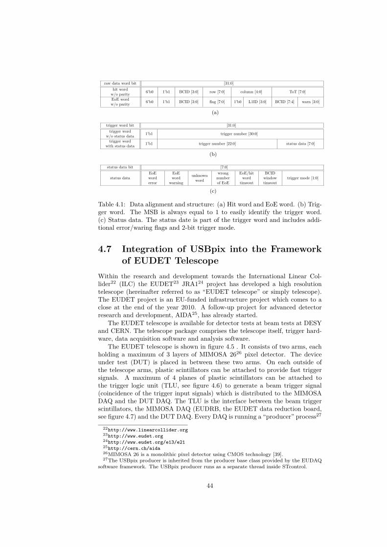
raw data word bit [31:0]hit word
w/o parity 6’b0 1’b1 BCID [3:0] row [7:0] column [4:0] ToT [7:0]
EoE wordw/o parity 6’b0 1’b1 BCID [3:0] flag [7:0] 1’b0 L1ID [3:0] BCID [7:4] warn [3:0]
(a)
trigger word bit [31:0]trigger word
w/o status data 1’b1 trigger number [30:0]
trigger wordwith status data 1’b1 trigger number [22:0] status data [7:0]
(b)
status data bit [7:0]
status dataEoEworderror
EoEword
warning
unknownword
wrongnumberof EoE
EoE/hitword
timeout
BCIDwindowtimeout
trigger mode [1:0]
(c)
Table 4.1: Data alignment and structure: (a) Hit word and EoE word. (b) Trig-ger word. The MSB is always equal to 1 to easily identify the trigger word.(c) Status data. The status date is part of the trigger word and includes addi-tional error/waring flags and 2-bit trigger mode.
4.7 Integration of USBpix into the Frameworkof EUDET Telescope
Within the research and development towards the International Linear Col-lider22 (ILC) the EUDET23 JRA124 project has developed a high resolutiontelescope (hereinafter referred to as “EUDET telescope” or simply telescope).The EUDET project is an EU-funded infrastructure project which comes to aclose at the end of the year 2010. A follow-up project for advanced detectorresearch and development, AIDA25, has already started.
The EUDET telescope is available for detector tests at beam tests at DESYand CERN. The telescope package comprises the telescope itself, trigger hard-ware, data acquisition software and analysis software.
The EUDET telescope is shown in figure 4.5 . It consists of two arms, eachholding a maximum of 3 layers of MIMOSA 2626 pixel detector. The deviceunder test (DUT) is placed in between these two arms. On each outside ofthe telescope arms, plastic scintillators can be attached to provide fast triggersignals. A maximum of 4 planes of plastic scintillators can be attached tothe trigger logic unit (TLU, see figure 4.6) to generate a beam trigger signal(coincidence of the trigger input signals) which is distributed to the MIMOSADAQ and the DUT DAQ. The TLU is the interface between the beam triggerscintillators, the MIMOSA DAQ (EUDRB, the EUDET data reduction board,see figure 4.7) and the DUT DAQ. Every DAQ is running a “producer” process27
22
http://www.linearcollider.org
23
http://www.eudet.org
24
http://www.eudet.org/e13/e21
25
http://cern.ch/aida
26MIMOSA 26 is a monolithic pixel detector using CMOS technology [39].27The USBpix producer is inherited from the producer base class provided by the EUDAQ
software framework. The USBpix producer runs as a separate thread inside STcontrol.
44
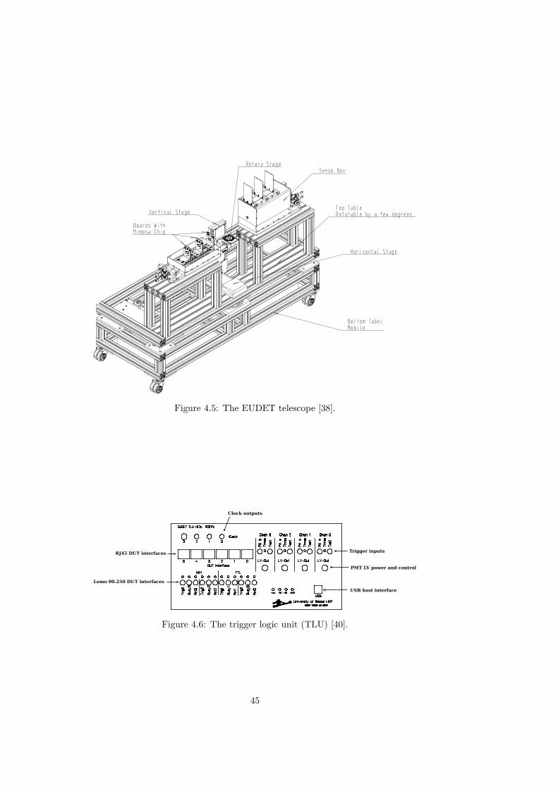
Figure 4.5: The EUDET telescope [38].
Figure 4.6: The trigger logic unit (TLU) [40].
45
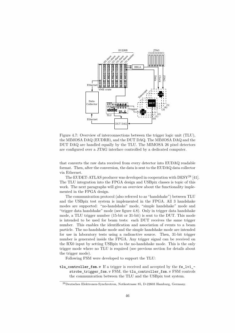
Figure 4.7: Overview of interconnections between the trigger logic unit (TLU),the MIMOSA DAQ (EUDRB), and the DUT DAQ. The MIMOSA DAQ and theDUT DAQ are handled equally by the TLU. The MIMOSA 26 pixel detectorsare configured over a JTAG interface controlled by a dedicated computer.
that converts the raw data received from every detector into EUDAQ readableformat. Then, after the conversion, the data is sent to the EUDAQ data collectorvia Ethernet.
The EUDET-ATLAS producer was developed in cooperation with DESY28 [41].The TLU integration into the FPGA design and USBpix classes is topic of thiswork. The next paragraphs will give an overview about the functionality imple-mented in the FPGA design.
The communication protocol (also referred to as “handshake”) between TLUand the USBpix test system is implemented in the FPGA. All 3 handshakemodes are supported: “no-handshake” mode, “simple handshake” mode and“trigger data handshake” mode (see figure 4.8). Only in trigger data handshakemode, a TLU trigger number (15-bit or 31-bit) is sent to the DUT. This modeis intended to be used for beam tests: each DUT receives the same triggernumber. This enables the identification and association of events to a beamparticle. The no-handshake mode and the simple handshake mode are intendedfor use in laboratory tests using a radioactive source. Then, 31-bit triggernumber is generated inside the FPGA. Any trigger signal can be received onthe RX0 input by setting USBpix to the no-handshake mode. This is the onlytrigger mode where no TLU is required (see previous section for details aboutthe trigger mode).
Following FSM were developed to support the TLU:
tlu_controller_fsm.v If a trigger is received and accepted by the fe_lv1_-strobe_trigger_fsm.v FSM, the tlu_controller_fsm.v FSM controlsthe communication between the TLU and the USBpix test system.
28Deutsches Elektronen-Synchrotron, Notkestrasse 85, D-22603 Hamburg, Germany.
46
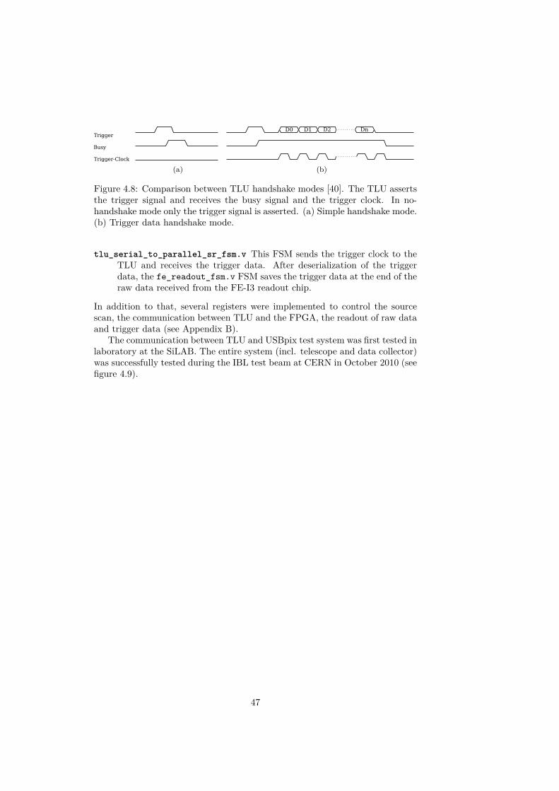
(a)
(b)
Figure 4.8: Comparison between TLU handshake modes [40]. The TLU assertsthe trigger signal and receives the busy signal and the trigger clock. In no-handshake mode only the trigger signal is asserted. (a) Simple handshake mode.(b) Trigger data handshake mode.
tlu_serial_to_parallel_sr_fsm.v This FSM sends the trigger clock to theTLU and receives the trigger data. After deserialization of the triggerdata, the fe_readout_fsm.v FSM saves the trigger data at the end of theraw data received from the FE-I3 readout chip.
In addition to that, several registers were implemented to control the sourcescan, the communication between TLU and the FPGA, the readout of raw dataand trigger data (see Appendix B).
The communication between TLU and USBpix test system was first tested inlaboratory at the SiLAB. The entire system (incl. telescope and data collector)was successfully tested during the IBL test beam at CERN in October 2010 (seefigure 4.9).
47
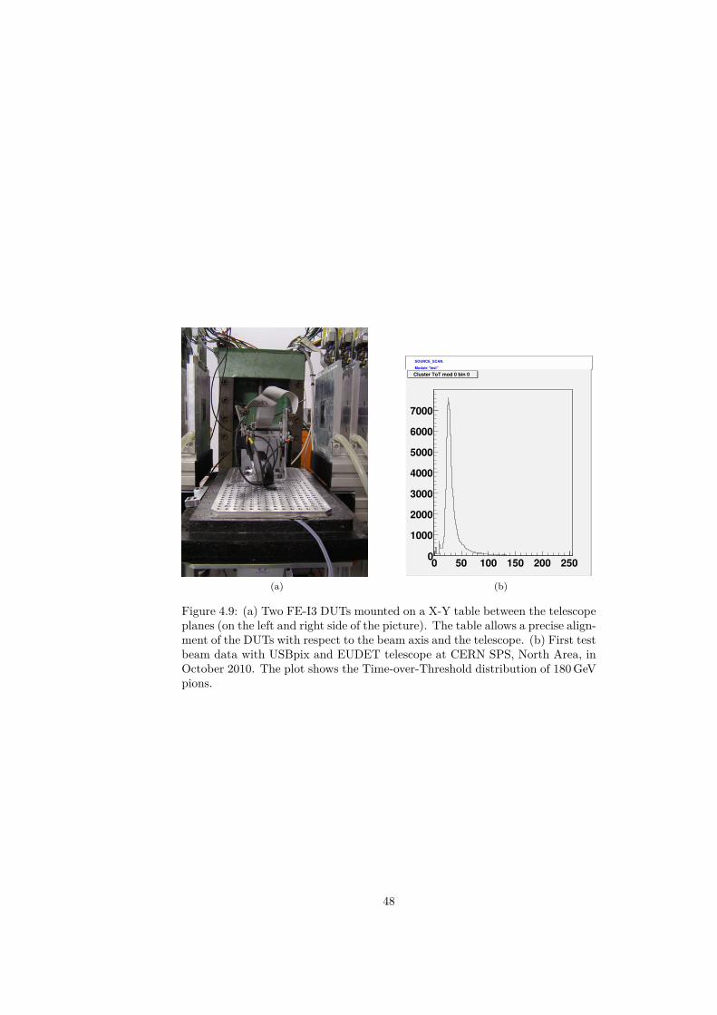
(a)
SOURCE_SCAN.
Module "test"
0 50 100 150 200 2500
1000
2000
3000
4000
5000
6000
7000
Cluster ToT mod 0 bin 0
(b)
Figure 4.9: (a) Two FE-I3 DUTs mounted on a X-Y table between the telescopeplanes (on the left and right side of the picture). The table allows a precise align-ment of the DUTs with respect to the beam axis and the telescope. (b) First testbeam data with USBpix and EUDET telescope at CERN SPS, North Area, inOctober 2010. The plot shows the Time-over-Threshold distribution of 180 GeVpions.
48
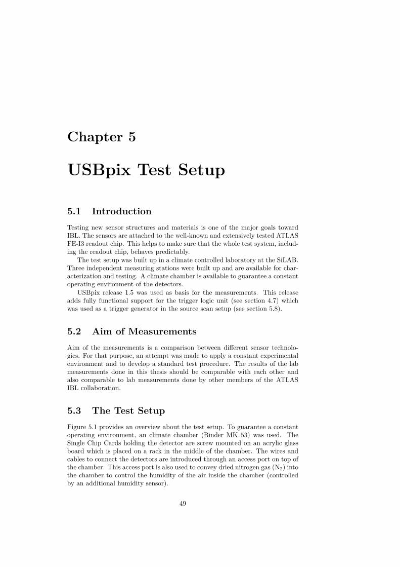
Chapter 5
USBpix Test Setup
5.1 IntroductionTesting new sensor structures and materials is one of the major goals towardIBL. The sensors are attached to the well-known and extensively tested ATLASFE-I3 readout chip. This helps to make sure that the whole test system, includ-ing the readout chip, behaves predictably.
The test setup was built up in a climate controlled laboratory at the SiLAB.Three independent measuring stations were built up and are available for char-acterization and testing. A climate chamber is available to guarantee a constantoperating environment of the detectors.
USBpix release 1.5 was used as basis for the measurements. This releaseadds fully functional support for the trigger logic unit (see section 4.7) whichwas used as a trigger generator in the source scan setup (see section 5.8).
5.2 Aim of MeasurementsAim of the measurements is a comparison between di�erent sensor technolo-gies. For that purpose, an attempt was made to apply a constant experimentalenvironment and to develop a standard test procedure. The results of the labmeasurements done in this thesis should be comparable with each other andalso comparable to lab measurements done by other members of the ATLASIBL collaboration.
5.3 The Test SetupFigure 5.1 provides an overview about the test setup. To guarantee a constantoperating environment, an climate chamber (Binder MK 53) was used. TheSingle Chip Cards holding the detector are screw mounted on an acrylic glassboard which is placed on a rack in the middle of the chamber. The wires andcables to connect the detectors are introduced through an access port on top ofthe chamber. This access port is also used to convey dried nitrogen gas (N
2
) intothe chamber to control the humidity of the air inside the chamber (controlledby an additional humidity sensor).
49
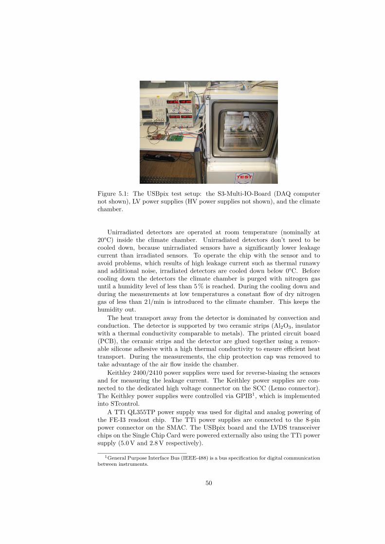
Figure 5.1: The USBpix test setup: the S3-Multi-IO-Board (DAQ computernot shown), LV power supplies (HV power supplies not shown), and the climatechamber.
Unirradiated detectors are operated at room temperature (nominally at20°C) inside the climate chamber. Unirradiated detectors don’t need to becooled down, because unirradiated sensors have a significantly lower leakagecurrent than irradiated sensors. To operate the chip with the sensor and toavoid problems, which results of high leakage current such as thermal runawyand additional noise, irradiated detectors are cooled down below 0°C. Beforecooling down the detectors the climate chamber is purged with nitrogen gasuntil a humidity level of less than 5 % is reached. During the cooling down andduring the measurements at low temperatures a constant flow of dry nitrogengas of less than 2 l/min is introduced to the climate chamber. This keeps thehumidity out.
The heat transport away from the detector is dominated by convection andconduction. The detector is supported by two ceramic strips (Al
2
O3
, insulatorwith a thermal conductivity comparable to metals). The printed circuit board(PCB), the ceramic strips and the detector are glued together using a remov-able silicone adhesive with a high thermal conductivity to ensure e�cient heattransport. During the measurements, the chip protection cap was removed totake advantage of the air flow inside the chamber.
Keithley 2400/2410 power supplies were used for reverse-biasing the sensorsand for measuring the leakage current. The Keithley power supplies are con-nected to the dedicated high voltage connector on the SCC (Lemo connector).The Keithley power supplies were controlled via GPIB1, which is implementedinto STcontrol.
A TTi QL355TP power supply was used for digital and analog powering ofthe FE-I3 readout chip. The TTi power supplies are connected to the 8-pinpower connector on the SMAC. The USBpix board and the LVDS transceiverchips on the Single Chip Card were powered externally also using the TTi powersupply (5.0 V and 2.8 V respectively).
1General Purpose Interface Bus (IEEE-488) is a bus specification for digital communicationbetween instruments.
50
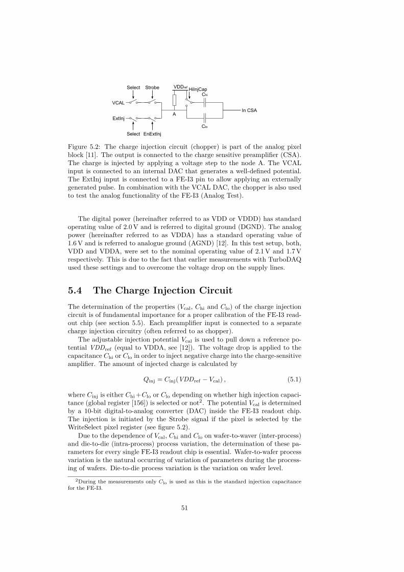
Figure 5.2: The charge injection circuit (chopper) is part of the analog pixelblock [11]. The output is connected to the charge sensitive preamplifier (CSA).The charge is injected by applying a voltage step to the node A. The VCALinput is connected to an internal DAC that generates a well-defined potential.The ExtInj input is connected to a FE-I3 pin to allow applying an externallygenerated pulse. In combination with the VCAL DAC, the chopper is also usedto test the analog functionality of the FE-I3 (Analog Test).
The digital power (hereinafter referred to as VDD or VDDD) has standardoperating value of 2.0 V and is referred to digital ground (DGND). The analogpower (hereinafter referred to as VDDA) has a standard operating value of1.6 V and is referred to analogue ground (AGND) [12]. In this test setup, both,VDD and VDDA, were set to the nominal operating value of 2.1 V and 1.7 Vrespectively. This is due to the fact that earlier measurements with TurboDAQused these settings and to overcome the voltage drop on the supply lines.
5.4 The Charge Injection CircuitThe determination of the properties (V
cal
, C
hi
and C
lo
) of the charge injectioncircuit is of fundamental importance for a proper calibration of the FE-I3 read-out chip (see section 5.5). Each preamplifier input is connected to a separatecharge injection circuitry (often referred to as chopper).
The adjustable injection potential V
cal
is used to pull down a reference po-tential VDD
ref
(equal to VDDA, see [12]). The voltage drop is applied to thecapacitance C
hi
or C
lo
in order to inject negative charge into the charge-sensitiveamplifier. The amount of injected charge is calculated by
Q
inj
= C
inj
(VDDref
≠ V
cal
) , (5.1)
where C
inj
is either C
hi
+C
lo
or C
lo
depending on whether high injection capaci-tance (global register [156]) is selected or not2. The potential V
cal
is determinedby a 10-bit digital-to-analog converter (DAC) inside the FE-I3 readout chip.The injection is initiated by the Strobe signal if the pixel is selected by theWriteSelect pixel register (see figure 5.2).
Due to the dependence of V
cal
, C
hi
and C
lo
on wafer-to-waver (inter-process)and die-to-die (intra-process) process variation, the determination of these pa-rameters for every single FE-I3 readout chip is essential. Wafer-to-wafer processvariation is the natural occurring of variation of parameters during the process-ing of wafers. Die-to-die process variation is the variation on wafer level.
2During the measurements only Clo
is used as this is the standard injection capacitancefor the FE-I3.
51
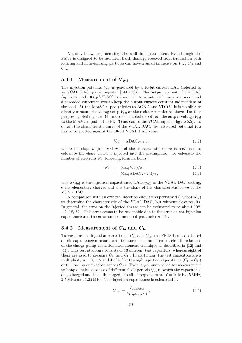
Not only the wafer processing a�ects all three parameters. Even though, theFE-I3 is designed to be radiation hard, damage received from irradiation withionizing and none-ionizing particles can have a small influence on V
cal
, C
hi
andC
lo
.
5.4.1 Measurement of Vcal
The injection potential V
cal
is generated by a 10-bit current DAC (referred toas VCAL DAC, global register [144:153]). The output current of the DAC(approximately 0.5 µA/DAC) is converted to a potential using a resistor anda cascoded current mirror to keep the output current constant independent ofthe load. At the MonVCal pad (diodes to AGND and VDDA) it is possible todirectly measure the voltage step V
cal
at the resistor mentioned above. For thatpurpose, global register [74] has to be enabled to redirect the output voltage V
cal
to the MonVCal pad of the FE-I3 (instead to the VCAL input in figure 5.2). Toobtain the characteristic curve of the VCAL DAC, the measured potential V
cal
has to be plotted against the 10-bit VCAL DAC value:
V
cal
= a DACVCAL
, (5.2)
where the slope a (in mV/DAC) of the characteristic curve is now used tocalculate the chare which is injected into the preamplifier. To calculate thenumber of electrons N
e
, following formula holds:
N
e
= (Cinj
V
cal
)/e , (5.3)= (C
inj
a DACVCAL
)/e , (5.4)
where C
inj
is the injection capacitance, DACVCAL
is the VCAL DAC setting,e the elementary charge, and a is the slope of the characteristic curve of theVCAL DAC.
A comparison with an external injection circuit was performed (TurboDAQ)to determine the characteristic of the VCAL DAC, but without clear results.In general, the error on the injected charge can be estimated to be about 10%[42, 18, 32]. This error seems to be reasonable due to the error on the injectioncapacitance and the error on the measured parameter a [43].
5.4.2 Measurement of Chi
and Clo
To measure the injection capacitance C
hi
and C
lo
, the FE-I3 has a dedicatedon-die capacitance measurement structure. The measurement circuit makes useof the charge-pump capacitor measurement technique as described in [12] and[44]. This test structure consists of 16 di�erent test capacitors, whereas eight ofthem are used to measure C
hi
and C
lo
. In particular, the test capacitors are amultiplicity n = 0, 1, 2 and 4 of either the high injection capacitance (C
hi
+C
lo
)or the low injection capacitance (C
lo
). The charge-pump capacitor measurementtechnique makes also use of di�erent clock periods 1
/f, in which the capacitor isonce charged and then discharged. Possible frequencies are f = 10 MHz, 5 MHz,2.5 MHz and 1.25 MHz. The injection capacitance is calculated by
C
test
= I
CapMeas
V
CapMeas
· f
, (5.5)
52
where C
test
is the capacitance equal to n · (Chi
+ C
lo
) or n · C
lo
, f is the fre-quency of the charging/discharging circuit, V
CapMeas
is the potential applied tothe CapMeas pad (usually 2 V, diodes to DGND3 and VDD) and I
CapMeas
isthe measured mean current. The multiplicity n and the charge/discharge fre-quency f can be set by global register [67:64] and [69:67], respectively. Thenominal value for the low injection capacitance C
lo
is 8 fF and for high injectioncapacitance (C
hi
+ C
lo
) is 40 fF.The measurement results of the test capacitor deviates by about 10% each
successive measurement. Also an error in the capacitance over the entire FE-I3 readout chip has to be considered, though it is not possible to measure theabsolute values for each pixel.
5.5 Tuning of the FE-I3Tuning of the FE-I3 means the calibration of the analog part of every readoutchannel on the FE-I3 readout chip. In other words, registers need to be adjustedin such a way that the preamplifier and discriminator of each pixel on the FE-I3readout chip operate in a limited range.
The tuning starts with a standard setup as given in Appendix A. The stan-dard tuning has a typical target threshold of 4000 e- and aims for a gain of60 bunch crossings4 (BC) Time-over-Threshold5 (ToT) at charge collection of20, 000 e- (colloquially referred to as “60 ToT at 20, 000 e-”). The charge of20, 000 e- is to be expected for a minimum ionizing particle (MIP) passingthrough bulk silicon of 250 µm thickness.
The standard tuning as described above is not su�cient for lab characteri-zation. The following points were changed compared to the standard tuning:
1. The threshold was lowered to 3200 e-. Apart from the fact that this thresh-old was chosen for former laboratory measurements and was used duringtest beam, there are several reasons for choosing a lower threshold: first,the threshold can be lowered to that value because there is no influenceof large detector system on the electronics of the device under test (thisincludes e�ects on noise and threshold dispersion). Second, for sensorcharacterization it is necessary to measure as much generated charge aspossible. The lower the threshold, the more pixels see a hit (increased hitprobability). In case of charge sharing between adjacent pixels the addi-tional measured charge can be assigned to the seed pixel (higher chargecollecting e�ciency). Third, the threshold of 3200 e- is a compromise be-tween charge collection e�ciency and noise occupancy (also referred toas noise hit rate, see [8]). As shown in [34], in case of unirradiated 3Dsensors, noise occupancy starts rising significantly from a threshold of ap-proximately 3200 e- and lower on.
3DGND is connected to AGND if jumper SJ16 of the Single Chip Card is closed.4The bunch crossing (BC) rate at LHC is 40 MHz and corresponds to a time of 25 ns.5The discriminator asserts a hit signal if the signal from the second amplifier is over a
certain threshold. The length of the hit signal is proportional to the amount of collectedcharge. The digital readout electronics generates a leading edge (LE) and trailing edge (TE)flag out of the hit signal. LE and TE are sent to the column arbitration unit (CAU) wherethe time between LE and TE is calculate by a 8-bit counter which is incremented every 25 ns(40 MHz). This time is called Time-over-Threshold (ToT) and is proportional to the collectedcharge.
53
2. The tuning was changed to a gain of 30 ToT at a collected charge of10, 000 e-. This tuning is comparable to the standard tuning (60 ToT at20, 000 e-) but for the ToT distribution a higher precision6 can be achievedfor shorter ToT which is the case for irradiated detectors. The generatedcharge for a MIP passing through a highly irradiated sensor material isexpected to be between 15 ke- and 19 ke- (250 µm bulk silicon, 1 MeV neu-tron equivalent fluence of 1 ◊ 1015cm≠2) caused by charge trapping [6].The charge seen per pixel is reduced even more due to charge sharingbetween adjacent pixels n[8]. Setting the tuning values of the ToT Cali-bration close to the expected charge is important to achieve high precisionmeasurement results (see also section 5.9.1 and 5.9.3).
During the tuning process the threshold of the discriminator and the feedbackcurrent of the preamplifier of each pixel get adjusted. The threshold is controlledby the GDAC global register and the TDAC pixel register. For tuning the ToTresponse, the feedback current of the preamplifier can be adjusted by changingthe IFDAC global register, the FDAC pixel register and the TrimIF globalregister. Changing the global register has an influence on the entire FE-I3readout chip (coarse tuning), while the pixel register determines the behaviorof a single pixel (fine tuning).
GDAC The GDAC is a 5-bit global DAC (global register [227:223], often re-ferred to as GlobalTDAC) controlling the threshold of the discriminatorfor every pixel (coarse tuning of the threshold). It covers a thresholdrange of 0–5000 e-. The standard value for GDAC is 16 and targets amean threshold of 4000 e- if all TDAC pixel registers are set to 64. Toreflect the lower target threshold of 3200 e-, which is used during charac-terization, the GDAC was manually set to 13. This will result in a TDACmean value close to 64 (in the middle of the TDAC range, see figure 5.3).
TDAC The TDAC is a 7-bit pixel register that determines the threshold ofeach pixel (fine tuning of the threshold). Within the range of 40 to 100,the TDAC DAC is linear and thus the threshold which depends on it [45].The GDAC must be set manually to a reasonable value, so that the TDACmean value (after tuning) is in the middle of its range (see figure 5.3).The TDAC tuning works as follows: for each pixel, a Threshold Scans isperformed at di�erent TDAC settings. The appropriate TDAC value isderived from the measured thresholds (linear regression).
IFDAC The IFDAC is an 8-bit global DAC (global register [132:125]) control-ling the feedback current of the preamplifier of every pixel (coarse tuningof the feedback current). Changing the IFDAC changes the collected ToT-to-charge calibration. The standard value is 32 and targets a charge ofapproximately 20, 000 e- that is expected for a MIP (TrimIF is set to 16).To obtain a gain of 30 ToT at a collected charge of 10, 000 e- the IFDACmust be manually set to a value equal or below 16. Setting the IFDAC toan appropriate value is of great importance for the FDAC tuning becauseof the limited range that is covered by the FDAC.
6This is due to the fact that the ToT-to-charge calibration is only linear in the first order(see section 5.9.1).
54
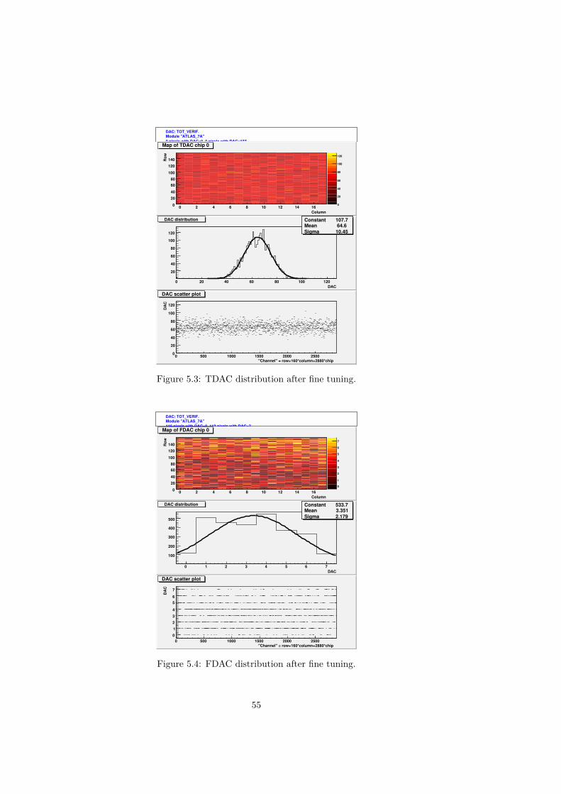
DAC: TOT_VERIF.Module "ATLAS_7A"0 pixels with DAC=0, 0 pixels with DAC=127
Column0 2 4 6 8 10 12 14 16
Row
0
2040
6080
100
120140
0
20
40
60
80
100
120
Map of TDAC chip 0
Constant 107.7Mean 64.6Sigma 10.45
DAC0 20 40 60 80 100 120
20
40
60
80
100
120
Constant 107.7Mean 64.6Sigma 10.45
DAC distribution
"Channel" = row+160*column+2880*chip0 500 1000 1500 2000 2500
DA
C
0
20
40
60
80
100
120
DAC scatter plot
Figure 5.3: TDAC distribution after fine tuning.
DAC: TOT_VERIF.Module "ATLAS_7A"116 pixels with DAC=0, 113 pixels with DAC=7
Column0 2 4 6 8 10 12 14 16
Row
0
2040
6080
100
120140
0
1
2
3
4
5
6
7
Map of FDAC chip 0
Constant 533.7Mean 3.351Sigma 2.179
DAC0 1 2 3 4 5 6 7
100
200
300
400
500
Constant 533.7Mean 3.351Sigma 2.179
DAC distribution
"Channel" = row+160*column+2880*chip0 500 1000 1500 2000 2500
DA
C
01234
56
7
DAC scatter plot
Figure 5.4: FDAC distribution after fine tuning.
55
FDAC The FDAC is a 3-bit pixel register that configures the feedback currentof the preamplifier of each pixel (fine tuning of the feedback current).IFDAC and TrimIF must be set in that way that the FDAC mean valueis in the middle of the FDAC range and that the minimum possible value(0) and the maximum possible value (7) is applied to a limited amount ofpixels (approximately 50). Changing the FDAC also results in a change ofthe threshold. As it is the case with the TDAC tuning, the FDAC tuningis done by an automatic tuning algorithm.
TrimIF The TrimIF is a global 8-bit DAC (global register [143:136], oftenreferred to as ITrimIf) that changes the step size of the FDAC, measuredin mA/DAC. TrimIF must be manually configured in that way, that thelimited range of the FDAC is fully covered (see figure 5.4). Changing theTrimIF involves a change of the IFDAC.
The entire tuning process is an iterational process that comprises several manualsteps to find appropriate values for the IFDAC and TrimIF. The last step isalways a combination of a TDAC tuning, FDAC tuning and TDAC tuning.This is because of the influence of the feedback current on the threshold.
After finishing the tuning, the threshold of each pixel is verified by runninga Threshold Scan (see next section). The threshold and noise are calculatedfor every single pixel. Also the mean value of the threshold distribution andthe width of the threshold distribution (‡
thr
) of all pixels are calculated. Asuccessful tuning results in a mean value only a few electrons away from thetarget threshold and has a ‡
thr
below 40 e-. The ToT-to-charge calibrationof each pixel is verified using a ToT Verification Scan that measures the ToTdistribution for a given amount of charge. For that purpose, the ToT VerificationScan injects a constant amount of charge into every preamplifier. The amountof charge is determined by the tuning parameters, e. g. 30 ToT at a collectedcharge of 10, 000 e-. Knowing the characteristic of the VCAL DAC (mV/DAC),a VCAL DAC value is calculated (mV/DAC) according to formula 5.1. Theinjection is repeated 200 times for every pixel to get the ToT distribution withhigh statistics. Also here, the mean value of the ToT distribution and the widthof the ToT distribution (‡
ToT
) of the entire pixel matrix are calculated. Typicalvalues for the mean value are less than 0.5 ToT away from the target ToT and‡
ToT
is equal or less than 1 ToT. The accuracy of the ToT response is limited bythe accuracy of the DACs (e. g. VCAL DAC) and is caused by variation of theinjection capacitance over the pixel matrix. The uniformity of the ToT responsecan only be achieved for a fixed amount of charge which is determined by thetuning parameters. See section 5.8 for more details.
5.6 Threshold Scan and Noise MeasurementsThe Threshold Scan plays an important role, first, to verify the threshold tun-ing of each pixel, and second, to measure the noise of every readout channel.Additionally, for the entire pixel matrix, a histogram of threshold distributionis generated to calculate the mean threshold and the width of the threshold dis-tribution. Both values are used to verify the overall performance of the tuningand the detector in general.
56
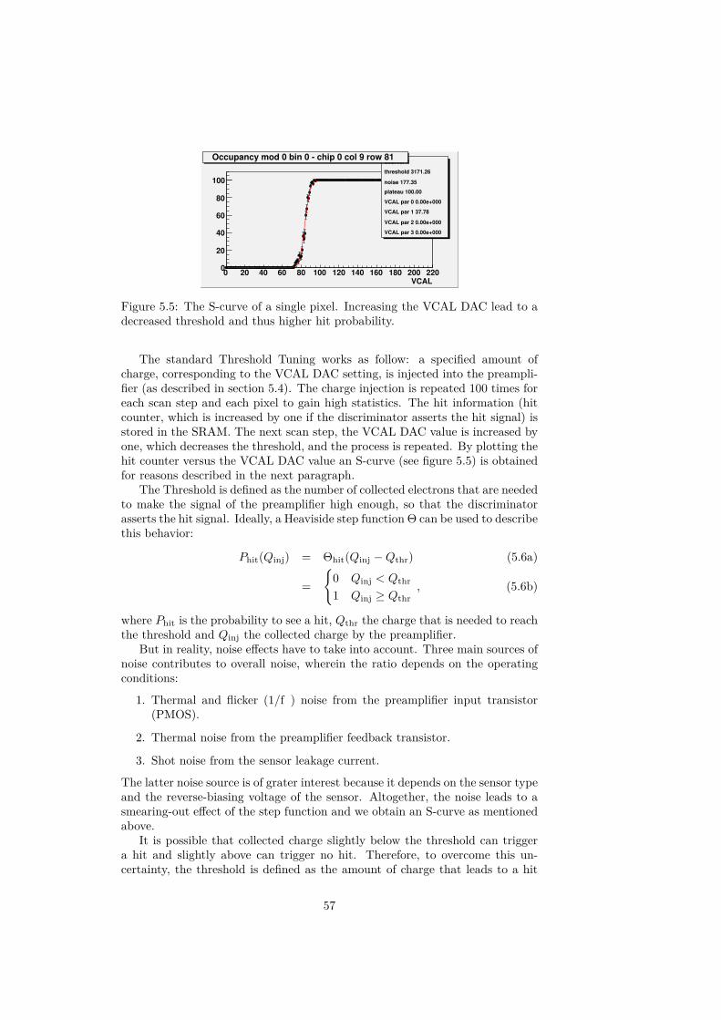
VCAL0 20 40 60 80 100 120 140 160 180 200 2200
20
40
60
80
100
ScurveFit
threshold 3171.26
noise 177.35
plateau 100.00
VCAL par 0 0.00e+000
VCAL par 1 37.78
VCAL par 2 0.00e+000
VCAL par 3 0.00e+000
Occupancy mod 0 bin 0 - chip 0 col 9 row 81
Figure 5.5: The S-curve of a single pixel. Increasing the VCAL DAC lead to adecreased threshold and thus higher hit probability.
The standard Threshold Tuning works as follow: a specified amount ofcharge, corresponding to the VCAL DAC setting, is injected into the preampli-fier (as described in section 5.4). The charge injection is repeated 100 times foreach scan step and each pixel to gain high statistics. The hit information (hitcounter, which is increased by one if the discriminator asserts the hit signal) isstored in the SRAM. The next scan step, the VCAL DAC value is increased byone, which decreases the threshold, and the process is repeated. By plotting thehit counter versus the VCAL DAC value an S-curve (see figure 5.5) is obtainedfor reasons described in the next paragraph.
The Threshold is defined as the number of collected electrons that are neededto make the signal of the preamplifier high enough, so that the discriminatorasserts the hit signal. Ideally, a Heaviside step function � can be used to describethis behavior:
P
hit
(Qinj
) = �hit
(Qinj
≠ Q
thr
) (5.6a)
=I
0 Q
inj
< Q
thr
1 Q
inj
Ø Q
thr
, (5.6b)
where P
hit
is the probability to see a hit, Q
thr
the charge that is needed to reachthe threshold and Q
inj
the collected charge by the preamplifier.But in reality, noise e�ects have to take into account. Three main sources of
noise contributes to overall noise, wherein the ratio depends on the operatingconditions:
1. Thermal and flicker (1/f ) noise from the preamplifier input transistor(PMOS).
2. Thermal noise from the preamplifier feedback transistor.
3. Shot noise from the sensor leakage current.
The latter noise source is of grater interest because it depends on the sensor typeand the reverse-biasing voltage of the sensor. Altogether, the noise leads to asmearing-out e�ect of the step function and we obtain an S-curve as mentionedabove.
It is possible that collected charge slightly below the threshold can triggera hit and slightly above can trigger no hit. Therefore, to overcome this un-certainty, the threshold is defined as the amount of charge that leads to a hit
57
probability of 50%. Mathematically, the probability P
hit
is given by convolutingthe Heaviside step function � with a normal (or Gaussian) distribution:
P
hit
(Qinj
) = �hit
(Qinj
≠ Q
thr
) ¢ expA
≠Q
2
inj
2‡
2
noise
B(5.7a)
= 12erfc
3Q
thr
≠ Q
injÔ2‡
noise
4. (5.7b)
The solution of the convolution is a complementary error function erfc(x) =(2/
Ôfi)´Œ
x
exp(≠t
2)dt, where ‡
noise
is the equivalent noise charge7 [46]. ‡
noise
is proportional to the slope of the S-curve at P
hit
= 50% and is typically in theorder of 160 e- (for planar sensors and for a pixel size of 50 ◊ 400 µm2). Thethreshold setting should be well above the overall noise to avoid fake hits dueto noise.
By plotting the threshold histogram, the mean threshold and threshold dis-persion ‡
thr
(root mean square, RMS) can be obtained assuming a normaldistribution. The threshold dispersion of an untuned FE-I3 readout chip isabout 600 e- and for a tuned chip it is less than 40 e-. The dispersion of thepixel-to-pixel threshold has a similar e�ect as noise, but it can be treated asa time-independent noise source [11]. The contribution to overall noise can beneglected in the case of a tuned chip.
Neither the threshold dispersion nor the noise depends on the target thresh-old [6]. But both are characteristic for the sensor type attached to the FE-I3readout chip. In case of the noise there is also dependence on the reverse-biasingof the sensor (see next chapter).
5.7 Bias Scan SetupThe purpose of the bias scan is to measure the leakage current of the entire pixelmatrix and pixel-wise (MONLEAK), noise, threshold, threshold dispersion andcrosstalk depending on the reverse-biasing voltage applied to the sensor.
The measurement was done using the Primitive List (often referred to asPrim List) functionality that is implemented in STcontrol. A Primitive List is alist of scans (e. g. Threshold Scan) and actions (e. g. setting the voltage, waitingfor a given amount of time) that defines the procedure of the scan. Items in thePrimitive List are processed in a sequence. The Primitive List used for the biasscan contains following steps:
1. Setting the reverse-biasing voltage
2. Waiting 5 (30) minutes
3. MONLEAK Scan
4. Configuring the readout chip
5. Waiting 1 minute7In High Energy Physics applications, the equivalent noise charge (ENC) is a convenient
way to express the noise-to-signal ratio of a charge sensitive amplifier and is given by theratio of root mean square (RMS) noise voltage V
RMS
to the signal pulse height Vmax
(qe
) fora charge signal of a single electron: ENC = V
RMS
/Vmax
(qe
).
58
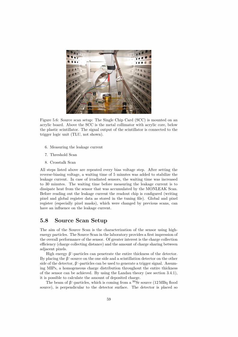
Figure 5.6: Source scan setup: The Single Chip Card (SCC) is mounted on anacrylic board. Above the SCC is the metal collimator with acrylic core, belowthe plastic scintillator. The signal output of the scintillator is connected to thetrigger logic unit (TLU, not shown).
6. Measuring the leakage current
7. Threshold Scan
8. Crosstalk Scan
All steps listed above are repeated every bias voltage step. After setting thereverse-biasing voltage, a waiting time of 5 minutes was added to stabilize theleakage current. In case of irradiated sensors, the waiting time was increasedto 30 minutes. The waiting time before measuring the leakage current is todissipate heat from the sensor that was accumulated by the MONLEAK Scan.Before reading out the leakage current the readout chip is configured (writingpixel and global register data as stored in the tuning file). Global and pixelregister (especially pixel masks), which were changed by previous scans, canhave an influence on the leakage current.
5.8 Source Scan SetupThe aim of the Source Scan is the characterization of the sensor using high-energy particles. The Source Scan in the laboratory provides a first impression ofthe overall performance of the sensor. Of greater interest is the charge collectione�ciency (charge collecting distance) and the amount of charge sharing betweenadjacent pixels.
High energy �--particles can penetrate the entire thickness of the detector.By placing the �--source on the one side and a scintillation detector on the otherside of the detector, �--particles can be used to generate a trigger signal. Assum-ing MIPs, a homogeneous charge distribution throughout the entire thicknessof the sensor can be achieved. By using the Landau theory (see section 3.4.1),it is possible to calculate the amount of deposited charge.
The beam of �--particles, which is coming from a 90Sr source (12 MBq floodsource), is perpendicular to the detector surface. The detector is placed so
59
that the particles first impinge the sensor. The particle beam is collimatedto a beam diameter of 1 mm. The collimator was placed so that the beamspot is in the middle of the pixel matrix. A plastic scintillator (Sc) attachedto a photomultiplier tube (PMT) is placed on the side faced away from thesource. The PMT output is connected to the TLU (see section 4.7) whichprocesses the trigger signal and communicates with the USBpix board (triggerdata handshake).
Also for this scan a Primitive List was set up:
1. Setting the reverse-biasing voltage
2. Waiting 5 (30) minutes
3. Source Scan
4. Configuring the readout chip
5. Waiting 1 minute
6. Measuring the leakage current
7. Threshold Scan
The same principles apply as described in the former section. The measurementof the leakage current and the Threshold Scan are for verification purposes. TheSource Scan was set up to take 500, 000 external triggers. The raw data wasstored to TurboDAQ-compatible output files (as described in section 4.4.3). Thethreshold of the discriminator, which is built into the trigger logic unit, was setto 150 mV, so that almost all noise hits coming from the PMT are suppressed.This results in an e�ective trigger rate8 of approximately 500 Hz (limited bythe TLU9). The total length of LV1 trigger was set to 16 bunch crossings (16consecutive triggers à 25 ns) and the delay of the LV1 trigger is set so thatfirst hit data approximately belongs to the third consecutive LV1 trigger (seefigure 5.7). Several pixel rows and columns were disabled during the SourceScan: column 0 and 17 (long pixels), row 153 to 159 (ganged and inter-gangedpixels), row 152 (also shows a higher noise induced by its neighbours) and row 0to 7 (in case of 3D sensors they show unpredictable behavior) were alwaysdisabled. In addition to that, any pixel with high noise or high hit occupancywas disabled.
5.9 Analysis of the Raw DataThe analysis of the raw data taken during the Source Scan (see former section)is important for the characterization of the sensor. During the analysis, the rawdata undergoes several steps:
1. Clustering of hits10 from the same particle.8E�ective trigger rate means accepted and processed triggers. This includes receiving raw
data from FE-I3 and writing the raw data to the SRAM.9An upper limit for the e�ective trigger rate of USBpix can be calculated:
40 Mbit/s/(255 bit + 17 · 26 bit) ¥ 57 kHz10A hit is understood as any kind of single pixel hit, so that the collected charge is over
the threshold. An event comprises all single pixel hits that are triggered by the same incidentparticle. In this case the charge is shared between the pixels.
60
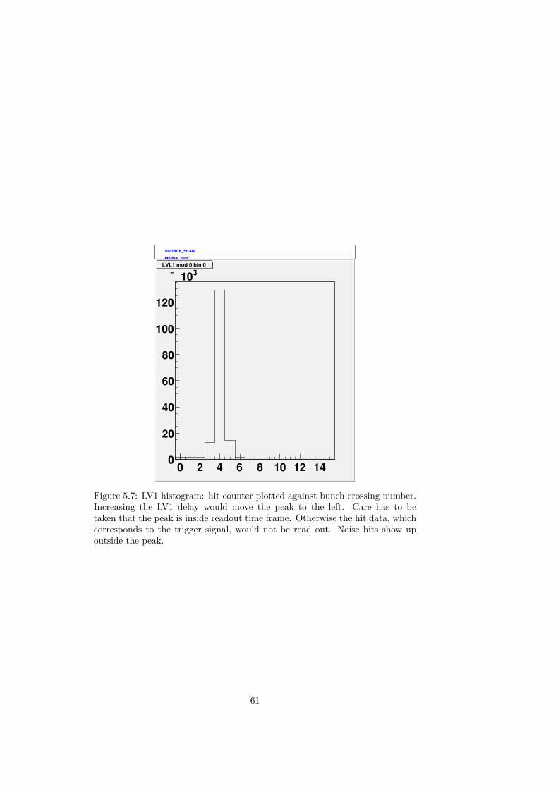
SOURCE_SCAN.
Module "test"
0 2 4 6 8 10 12 140
20
40
60
80
100
120
310LVL1 mod 0 bin 0
Figure 5.7: LV1 histogram: hit counter plotted against bunch crossing number.Increasing the LV1 delay would move the peak to the left. Care has to betaken that the peak is inside readout time frame. Otherwise the hit data, whichcorresponds to the trigger signal, would not be read out. Noise hits show upoutside the peak.
61

2. Conversion of (clustered) Time-over-Threshold to charge (ToT-to-chargeconversion).
3. Analysis of the clustered hit data and generation of the histograms.
The analysis software11 was developed in cooperation with CERN12. It is writ-ten in C++ and is using ROOT macros which are executed in the ROOT Cinterpreter (CINT). The analysis software splits into two parts: first, a ROOTmacro analyzes the raw data file and saves the clustered hit information to aROOT container file (first step, see section 5.9.2). A second ROOT macro thatreads in the clustered hit data and the ToT calibration data converts ToT intocharge and generates the histograms (latter two steps, see section 5.9.3).
5.9.1 ToT CalibrationAfter the tuning of the pixel mask and before starting the Source Scans, aToT Calibration Scan was performed. The ToT Calibration measures the ToTresponse of each pixel to a wide range of electric charge injected into the pream-plifier. This is in contrast to the ToT Verification Scan, where only a fixedamount of charge, given by the tuning parameters, is injected (see section 5.5).Even though the ToT response for a given charge has been adjusted by theFDAC tuning and is uniform over the entire pixel matrix (e. g. 30 ToT at a col-lected charge of 10, 000 e-), there are still di�erences in the ToT response. Thepixel-to-pixel di�erences in ToT increases the more the charge deviates from thevalue determined by the tuning parameter. Therefore, it is su�cient to measureover a wide range the relationship between injected charge and the correlatingToT response for each pixel.
The empirical [42] ToT calibration function13 is
ToT(Ne
) = A
3N
e
+ B
N
e
+ C
4, (5.8)
where ToT is the response in units of bunch crossings, N
e
the number of injectedelectrons. The parameters A, B and C are fit parameters and are unique for eachpixel. The fit parameters are strongly correlated [43]. For each fit parameter A,B or C, the data for the entire pixel matrix is stored in a ROOT macro and islater used for the ToT-to-charge calibration (see section 5.9.3).
5.9.2 Charge Sharing and ClusteringA particle, which passes the sensor, generates charge along its path. The chargecan be shared between neighboring pixel cells (so called charge sharing) for thefollowing reasons:
1. The point of impact is located at the border between two or more pixelcells.
2. A �-electron deposit energy along its path inside the sensor.11Source code as of December 8, 2010.12Christian Gallrapp, CERN, PH & DT Department, CH-1211, Genève 23, Switzerland.13Also used in the current ATLAS DAQ firmware.
62
3. The incident angle of the particle is not perpendicular to the sensor surfaceso that the particle passes several pixel cells.
The latter can be excluded due to the construction of the source scan setup. Incase of charge sharing between adjacent pixel cells, the resulting cluster is mostlikely composed of a high-charge hit (seed pixel) and one or more low-chargehits. But it cannot be precluded that the collected charge in the low-charge hitsis below the threshold and therefore is not recognized at all.
Another e�ect, which has influence on the clustering, is the timewalk e�ect.The timewalk e�ect is related to the rise time of the preamplifier. The time-walk e�ect is the dependence of the time, that the preamplifier output signalneeds to cross the discriminator threshold, on the maximum pulse height of thepreamplifier output signal. In other words, the recognition time of a hit and theassignment to a bunch crossing interval depends on the collected charge of thepreamplifier. To assign as many hits that were induced by the same particle aspossible to the corresponding bunch crossing interval, it is necessary to adjustthe phase of the 40 MHz clock (XCK) with respect to the bunch crossing. Thisis of great importance for the operation at the LHC, where only hits associatedto a single LV1 trigger (within 25 ns) are read out. The loss of the low-chargehits, which are a�ected by the timewalk e�ect if the clock phase is adjustedcorrectly, prevents the usage of charge interpolation to improve the single pointresolution [47]. To recover these hits, a timewalk correction is implemented inthe FE-I3 electronics (global register [219:220]). For hits with a ToT less thanor equal to a certain threshold (ThrDub, global register [211:218]), the hit issent twice to the end of column (EOC) bu�er: one with the original LE timestamp information and another assigned to the previous bunch crossing (LEtime stamp subtracted by one). Another mode allows the rejection of all hitswith a ToT below a certain threshold (ThrMin, global register [203:210]). It ispossible to operate both modes at the same time.
However, the automatic correction is inappropriate for laboratory character-ization (and in most cases for beam tests) where particles crossing the sensorhave a random phase with respect to the XCK. The timewalk e�ect therefore isnot limited to a certain input signal charge.
The task of the clustering algorithm is to cluster hit information, which isdistributed in space and time, to restore the total charge that was generated by acrossing particle. It has to be emphasized that for a laboratory characterization,the total amount of charge is of interest, whereas in HEP experiments the singlepoint resolution is of greater interest (which also takes advantage of the ToT).
5.9.3 Analysis and HistogrammingAccording to formula 5.8, the collected charge that corresponds to a distinctToT is
N
e
(ToT) = AB ≠ C ToTToT ≠ A
. (5.9)
By definition, a ToT of 1 corresponds to threshold charge defined by the tuningparameter, i. e. N
e
= 3200 e-. By entering the parameters A, B, and C forevery single pixel into equation 5.9, one can calculate the collected charge. Byentering ToT = 1 in the formula, the calculated result deviates by about 30 % ofthe expected charge of 3200 e≠. At a ToT of 30 the results deviate by about 1 %
63

from the expected charge of 10000 e≠. Especially for a small amount of charge,the empirical calibration function (equation 5.8) does not reflect the reality verywell (e. g. non-linearities of the DACs and amplifiers).
After the ToT-to-charge conversion, the analysis of the clustered hit data isproceeded. The analysis includes the generation of hit maps, hit histograms,cluster size distributions and ToT distributions of di�erent cluster sizes. Themost important aspect is the calculation of the most probable value (MPV). TheMPV is calculated by fitting a Landau distribution to the ToT distribution. Totake noise e�ects (e.g. electronic noise) into account the Landau distribution isconvoluted with a Gaussian (“Langau”).
64
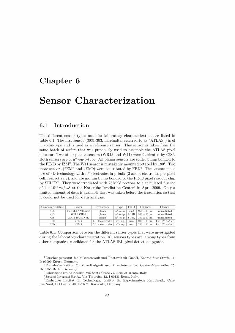
Chapter 6
Sensor Characterization
6.1 IntroductionThe di�erent sensor types used for laboratory characterization are listed intable 6.1. The first sensor (3631-303, hereinafter referred to as “ATLAS”) is ofn+-on-n-type and is used as a reference sensor. This sensor is taken from thesame batch of wafers that was previously used to assemble the ATLAS pixeldetector. Two other planar sensors (WR13 and W11) were fabricated by CiS1.Both sensors are of n+-on-p-type. All planar sensors are solder bump bonded tothe FE-I3 by IZM2. The W11 sensor is mistakenly mounted rotated by 180°. Twomore sensors (2EM6 and 4EM9) were contributed by FBK3. The sensors makeuse of 3D technology with n+-electrodes in p-bulk (2 and 4 electrodes per pixelcell, respectively), and are indium bump bonded to the FE-I3 pixel readout chipby SELEX4. They were irradiated with 25 MeV protons to a calculated fluenceof 1 ◊ 1015
neq/cm
2 at the Karlsruhe Irradiation Center5 in April 2009. Only alimited amount of data is available that was taken before the irradiation so thatit could not be used for data analysis.
Company/Institute Sensor Technology Type FE-I3 Thickness FluenceCiS 3631-303 “ATLAS” planar n+-on-n 5-7A 256 ± 10 µm unirradiatedCiS W11 19GR-2 planar n+-on-p 8-13B 300 ± 10 µm unirradiatedCiS WR13 19GR-NM2 planar n+-on-p 8-10A 300 ± 10 µm unirradiated
FBK 2EM6 3D, 2 electrodes n+-in-p n/a 200 ± 10 µm 1 ◊ 1015
neq/cm
2
FBK 4EM9 3D, 4 electrodes n+-in-p n/a 200 ± 10 µm 1 ◊ 1015
neq/cm
2
Table 6.1: Comparison between the di�erent sensor types that were investigatedduring the laboratory characterization. All sensors types are, among types fromother companies, candidates for the ATLAS IBL pixel detector upgrade.
1Forschungsinstitut für Mikrosensorik und Photovoltaik GmbH, Konrad-Zuse-Straße 14,D-99099 Erfurt, Germany.
2Fraunhofer-Institut für Zuverlässigkeit und Mikrointegration, Gustav-Meyer-Allee 25,D-13355 Berlin, Germany.
3Fondazione Bruno Kessler, Via Santa Croce 77, I-38122 Trento, Italy.4Sistemi Integrati S.p.A., Via Tiburtina 12, I-00131 Rome, Italy.5Karlsruher Institut für Technologie, Institut für Experimentelle Kernphysik, Cam-
pus Nord, PO Box 36 40, D-76021 Karlsruhe, Germany.
65
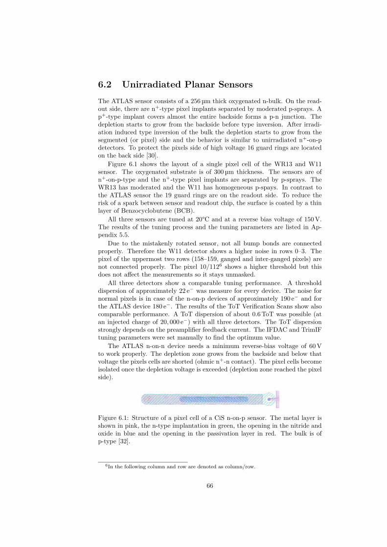
6.2 Unirradiated Planar SensorsThe ATLAS sensor consists of a 256 µm thick oxygenated n-bulk. On the read-out side, there are n+-type pixel implants separated by moderated p-sprays. Ap+-type implant covers almost the entire backside forms a p-n junction. Thedepletion starts to grow from the backside before type inversion. After irradi-ation induced type inversion of the bulk the depletion starts to grow from thesegmented (or pixel) side and the behavior is similar to unirradiated n+-on-pdetectors. To protect the pixels side of high voltage 16 guard rings are locatedon the back side [30].
Figure 6.1 shows the layout of a single pixel cell of the WR13 and W11sensor. The oxygenated substrate is of 300 µm thickness. The sensors are ofn+-on-p-type and the n+-type pixel implants are separated by p-sprays. TheWR13 has moderated and the W11 has homogeneous p-spays. In contrast tothe ATLAS sensor the 19 guard rings are on the readout side. To reduce therisk of a spark between sensor and readout chip, the surface is coated by a thinlayer of Benzocyclobutene (BCB).
All three sensors are tuned at 20°C and at a reverse bias voltage of 150 V.The results of the tuning process and the tuning parameters are listed in Ap-pendix 5.5.
Due to the mistakenly rotated sensor, not all bump bonds are connectedproperly. Therefore the W11 detector shows a higher noise in rows 0–3. Thepixel of the uppermost two rows (158–159, ganged and inter-ganged pixels) arenot connected properly. The pixel 10/1126 shows a higher threshold but thisdoes not a�ect the measurements so it stays unmasked.
All three detectors show a comparable tuning performance. A thresholddispersion of approximately 22 e≠ was measure for every device. The noise fornormal pixels is in case of the n-on-p devices of approximately 190 e≠ and forthe ATLAS device 180 e≠. The results of the ToT Verification Scans show alsocomparable performance. A ToT dispersion of about 0.6 ToT was possible (atan injected charge of 20, 000 e≠) with all three detectors. The ToT dispersionstrongly depends on the preamplifier feedback current. The IFDAC and TrimIFtuning parameters were set manually to find the optimum value.
The ATLAS n-on-n device needs a minimum reverse-bias voltage of 60 Vto work properly. The depletion zone grows from the backside and below thatvoltage the pixels cells are shorted (ohmic n+-n contact). The pixel cells becomeisolated once the depletion voltage is exceeded (depletion zone reached the pixelside).
Figure 6.1: Structure of a pixel cell of a CiS n-on-p sensor. The metal layer isshown in pink, the n-type implantation in green, the opening in the nitride andoxide in blue and the opening in the passivation layer in red. The bulk is ofp-type [32].
6In the following column and row are denoted as column/row.
66
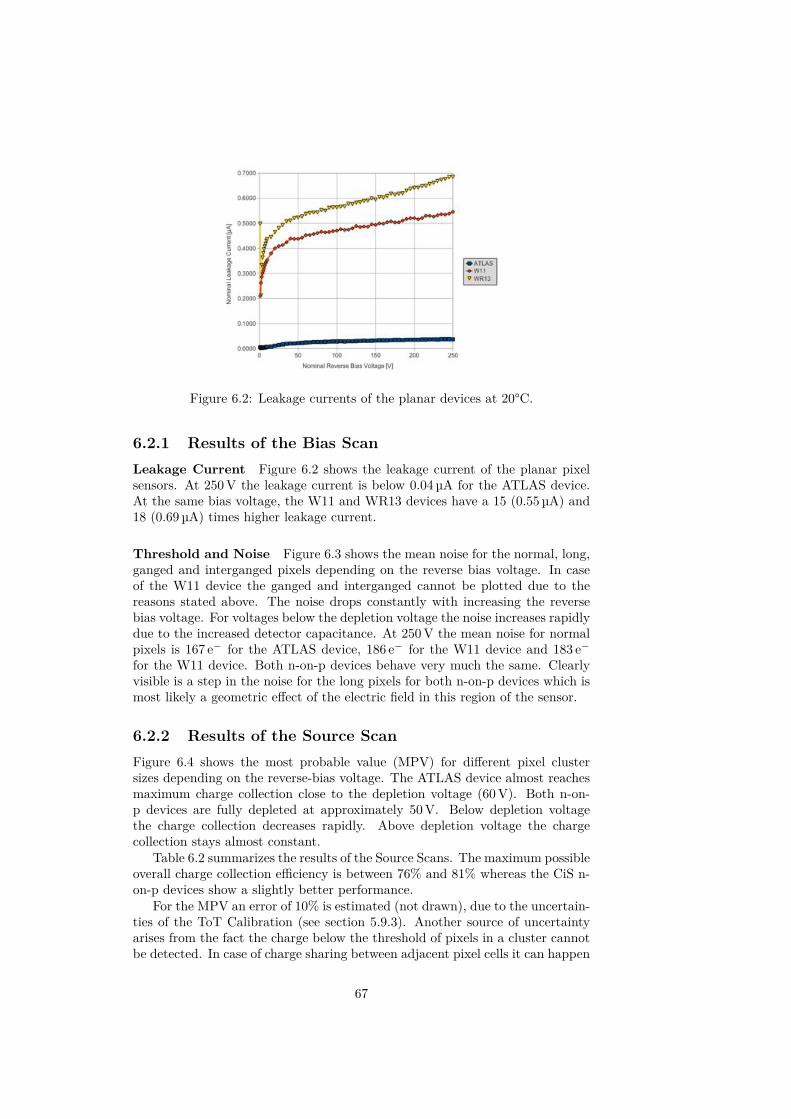
Figure 6.2: Leakage currents of the planar devices at 20°C.
6.2.1 Results of the Bias ScanLeakage Current Figure 6.2 shows the leakage current of the planar pixelsensors. At 250 V the leakage current is below 0.04 µA for the ATLAS device.At the same bias voltage, the W11 and WR13 devices have a 15 (0.55 µA) and18 (0.69 µA) times higher leakage current.
Threshold and Noise Figure 6.3 shows the mean noise for the normal, long,ganged and interganged pixels depending on the reverse bias voltage. In caseof the W11 device the ganged and interganged cannot be plotted due to thereasons stated above. The noise drops constantly with increasing the reversebias voltage. For voltages below the depletion voltage the noise increases rapidlydue to the increased detector capacitance. At 250 V the mean noise for normalpixels is 167 e≠ for the ATLAS device, 186 e≠ for the W11 device and 183 e≠
for the W11 device. Both n-on-p devices behave very much the same. Clearlyvisible is a step in the noise for the long pixels for both n-on-p devices which ismost likely a geometric e�ect of the electric field in this region of the sensor.
6.2.2 Results of the Source ScanFigure 6.4 shows the most probable value (MPV) for di�erent pixel clustersizes depending on the reverse-bias voltage. The ATLAS device almost reachesmaximum charge collection close to the depletion voltage (60 V). Both n-on-p devices are fully depleted at approximately 50 V. Below depletion voltagethe charge collection decreases rapidly. Above depletion voltage the chargecollection stays almost constant.
Table 6.2 summarizes the results of the Source Scans. The maximum possibleoverall charge collection e�ciency is between 76% and 81% whereas the CiS n-on-p devices show a slightly better performance.
For the MPV an error of 10% is estimated (not drawn), due to the uncertain-ties of the ToT Calibration (see section 5.9.3). Another source of uncertaintyarises from the fact the charge below the threshold of pixels in a cluster cannotbe detected. In case of charge sharing between adjacent pixel cells it can happen
67
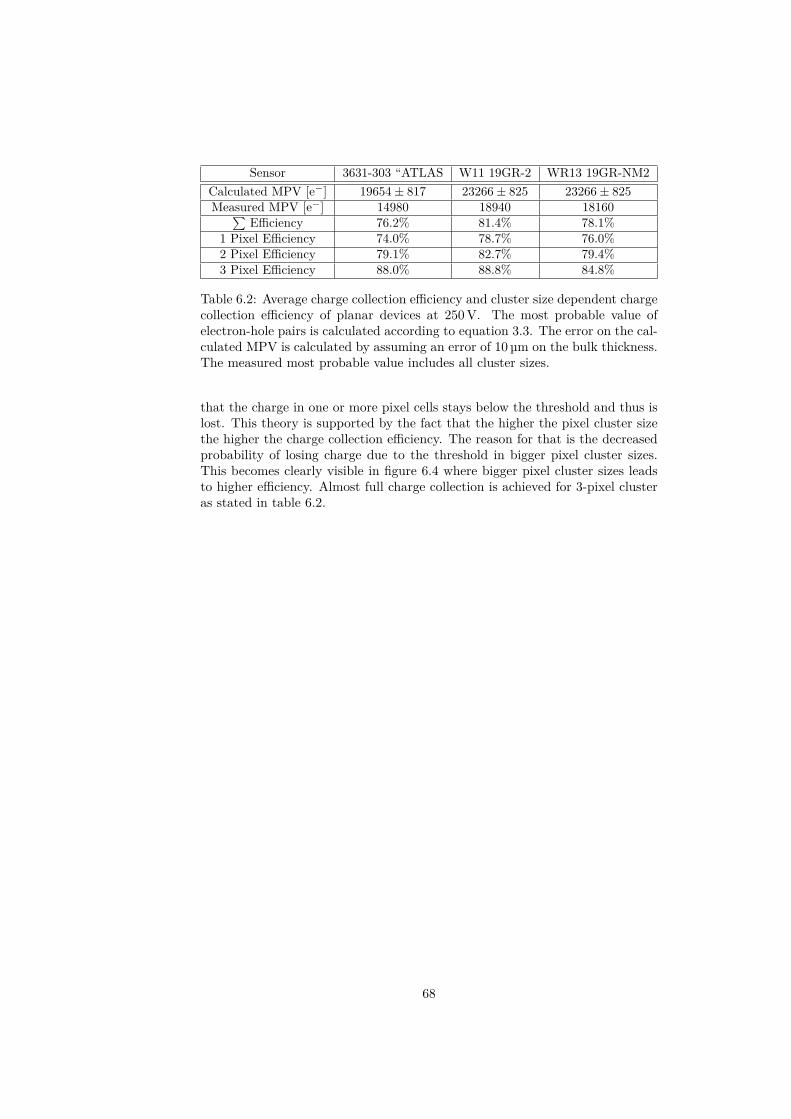
Sensor 3631-303 “ATLAS W11 19GR-2 WR13 19GR-NM2Calculated MPV [e≠] 19654 ± 817 23266 ± 825 23266 ± 825Measured MPV [e≠] 14980 18940 18160q
E�ciency 76.2% 81.4% 78.1%1 Pixel E�ciency 74.0% 78.7% 76.0%2 Pixel E�ciency 79.1% 82.7% 79.4%3 Pixel E�ciency 88.0% 88.8% 84.8%
Table 6.2: Average charge collection e�ciency and cluster size dependent chargecollection e�ciency of planar devices at 250 V. The most probable value ofelectron-hole pairs is calculated according to equation 3.3. The error on the cal-culated MPV is calculated by assuming an error of 10 µm on the bulk thickness.The measured most probable value includes all cluster sizes.
that the charge in one or more pixel cells stays below the threshold and thus islost. This theory is supported by the fact that the higher the pixel cluster sizethe higher the charge collection e�ciency. The reason for that is the decreasedprobability of losing charge due to the threshold in bigger pixel cluster sizes.This becomes clearly visible in figure 6.4 where bigger pixel cluster sizes leadsto higher e�ciency. Almost full charge collection is achieved for 3-pixel clusteras stated in table 6.2.
68
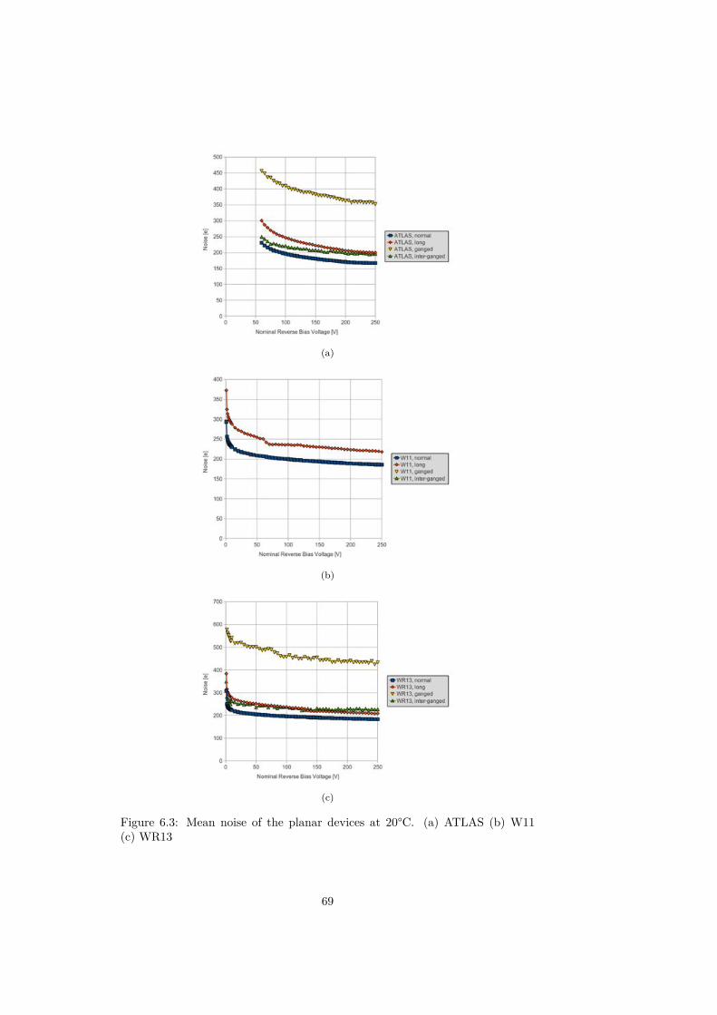
(a)
(b)
(c)
Figure 6.3: Mean noise of the planar devices at 20°C. (a) ATLAS (b) W11(c) WR13
69
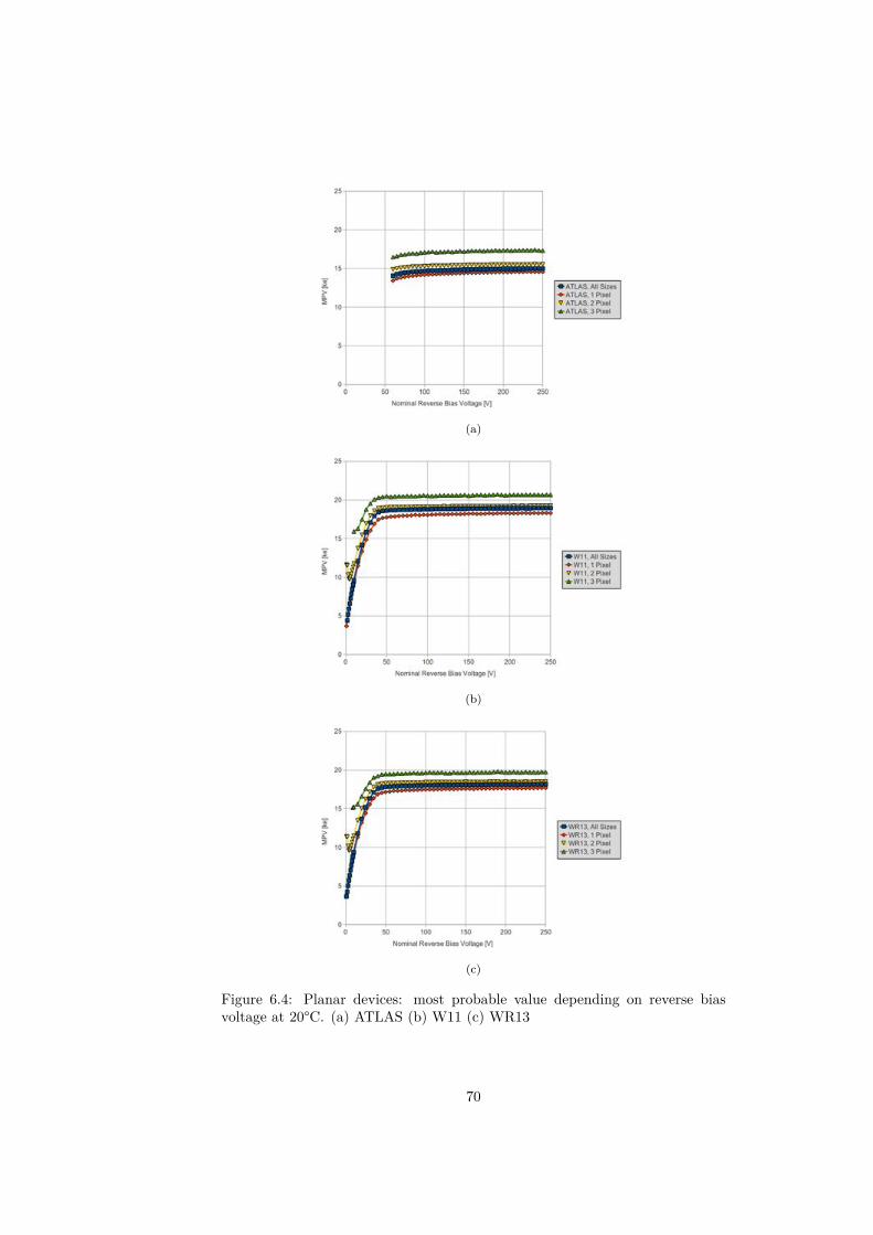
(a)
(b)
(c)
Figure 6.4: Planar devices: most probable value depending on reverse biasvoltage at 20°C. (a) ATLAS (b) W11 (c) WR13
70
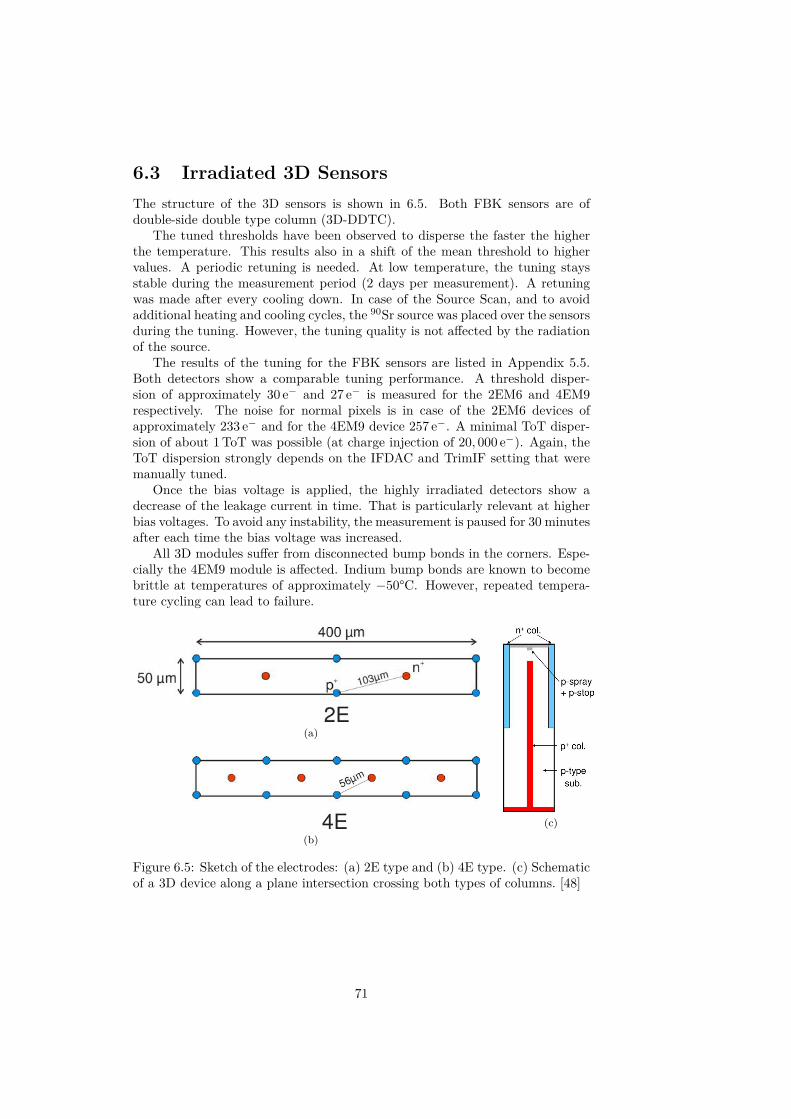
6.3 Irradiated 3D SensorsThe structure of the 3D sensors is shown in 6.5. Both FBK sensors are ofdouble-side double type column (3D-DDTC).
The tuned thresholds have been observed to disperse the faster the higherthe temperature. This results also in a shift of the mean threshold to highervalues. A periodic retuning is needed. At low temperature, the tuning staysstable during the measurement period (2 days per measurement). A retuningwas made after every cooling down. In case of the Source Scan, and to avoidadditional heating and cooling cycles, the 90Sr source was placed over the sensorsduring the tuning. However, the tuning quality is not a�ected by the radiationof the source.
The results of the tuning for the FBK sensors are listed in Appendix 5.5.Both detectors show a comparable tuning performance. A threshold disper-sion of approximately 30 e≠ and 27 e≠ is measured for the 2EM6 and 4EM9respectively. The noise for normal pixels is in case of the 2EM6 devices ofapproximately 233 e≠ and for the 4EM9 device 257 e≠. A minimal ToT disper-sion of about 1 ToT was possible (at charge injection of 20, 000 e≠). Again, theToT dispersion strongly depends on the IFDAC and TrimIF setting that weremanually tuned.
Once the bias voltage is applied, the highly irradiated detectors show adecrease of the leakage current in time. That is particularly relevant at higherbias voltages. To avoid any instability, the measurement is paused for 30 minutesafter each time the bias voltage was increased.
All 3D modules su�er from disconnected bump bonds in the corners. Espe-cially the 4EM9 module is a�ected. Indium bump bonds are known to becomebrittle at temperatures of approximately ≠50°C. However, repeated tempera-ture cycling can lead to failure.
(a)
(b)(c)
Figure 6.5: Sketch of the electrodes: (a) 2E type and (b) 4E type. (c) Schematicof a 3D device along a plane intersection crossing both types of columns. [48]
71
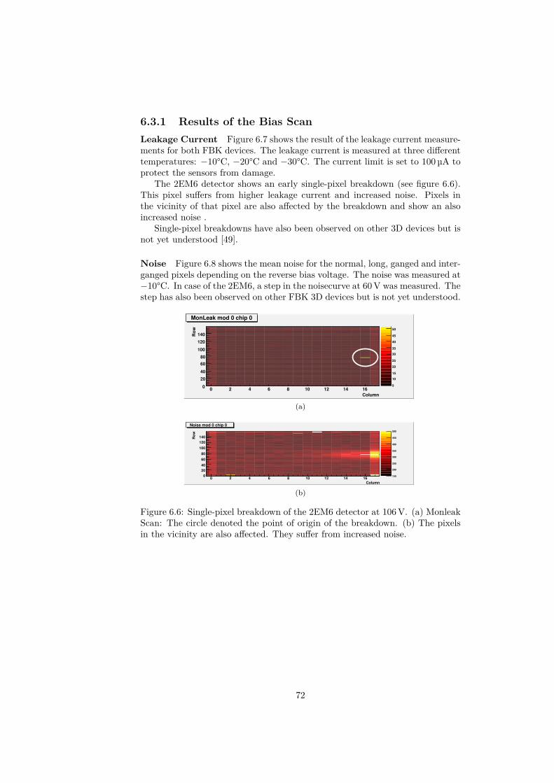
6.3.1 Results of the Bias ScanLeakage Current Figure 6.7 shows the result of the leakage current measure-ments for both FBK devices. The leakage current is measured at three di�erenttemperatures: ≠10°C, ≠20°C and ≠30°C. The current limit is set to 100 µA toprotect the sensors from damage.
The 2EM6 detector shows an early single-pixel breakdown (see figure 6.6).This pixel su�ers from higher leakage current and increased noise. Pixels inthe vicinity of that pixel are also a�ected by the breakdown and show an alsoincreased noise .
Single-pixel breakdowns have also been observed on other 3D devices but isnot yet understood [49].
Noise Figure 6.8 shows the mean noise for the normal, long, ganged and inter-ganged pixels depending on the reverse bias voltage. The noise was measured at≠10°C. In case of the 2EM6, a step in the noisecurve at 60 V was measured. Thestep has also been observed on other FBK 3D devices but is not yet understood.
Column0 2 4 6 8 10 12 14 16
Row
0
2040
6080
100
120140
5
10
15
20
25
30
35
40
45
50
MonLeak mod 0 chip 0
(a)
Column0 2 4 6 8 10 12 14 16
Row
020406080
100120140
150
200
250
300
350
400
450
500
Noise mod 0 chip 0
(b)
Figure 6.6: Single-pixel breakdown of the 2EM6 detector at 106 V. (a) MonleakScan: The circle denoted the point of origin of the breakdown. (b) The pixelsin the vicinity are also a�ected. They su�er from increased noise.
72
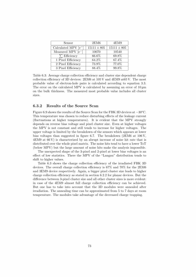
Sensor 2EM6 4EM9Calculated MPV [e≠] 15111 ± 805 15111 ± 805Measured MPV [e≠] 10070 10540q
E�ciency 66.6% 69.8%1 Pixel E�ciency 64.2% 67.4%2 Pixel E�ciency 73.9% 77.0%3 Pixel E�ciency 88.4% 99.8%
Table 6.3: Average charge collection e�ciency and cluster size dependent chargecollection e�ciency of 3D devices: 2EM6 at 105 V and 4EM9 at65 V. The mostprobable value of electron-hole pairs is calculated according to equation 3.3.The error on the calculated MPV is calculated by assuming an error of 10 µmon the bulk thickness. The measured most probable value includes all clustersizes.
6.3.2 Results of the Source ScanFigure 6.9 shows the results of the Source Scan for the FBK 3D devices at ≠30°C.This temperature was chosen to reduce disturbing e�ects of the leakage current(fluctuations at higher temperatures). It is evident that the MPV stronglydepends on reverse bias voltage and pixel cluster size. Even at higher voltagesthe MPV is not constant and still tends to increase for higher voltages. Theupper voltage is limited by the breakdown of the sensors which appears at lowerbias voltages than suggested in figure 6.7. The breakdown (2EM6 at 106 V,4EM9 at 66 V) is characterized by an abrupt increase of noise hit rate that isdistributed over the whole pixel matrix. The noise hits tend to have a lower ToT(below MPV) but the large amount of noise hits make the analysis impossible.
The unexpected shape of the 3-pixel and 2-pixel at lower bias voltages is ane�ect of low statistics. There the MPV of the “Langau” distribution tends toshift to higher values.
Table 6.3 shows the charge collection e�ciency of the irradiated FBK 3Ddevices. The overall charge collection e�ciency is 67% and 70% for the 2EM6and 3EM9 device respectively. Again, a bigger pixel cluster size leads to highercharge collection e�ciency as stated in section 6.2.2 for planar devices. But thedi�erence between 3-pixel cluster size and all other cluster sizes is more evident:in case of the 4EM9 almost full charge collection e�ciency can be achieved.But one has to take into account that the 3D modules were annealed afterirradiation. The annealing time can be approximated from 5 to 7 days at roomtemperature. The modules take advantage of the decreased charge trapping.
73
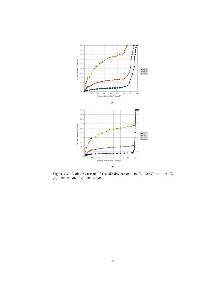
(a)
(b)
Figure 6.7: Leakage current of the 3D devices at ≠10°C, ≠20°C and ≠30°C.(a) FBK 2EM6. (b) FBK 4EM9.
74
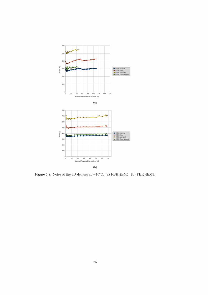
(a)
(b)
Figure 6.8: Noise of the 3D devices at ≠10°C. (a) FBK 2EM6. (b) FBK 4EM9.
75
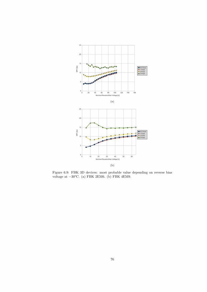
(a)
(b)
Figure 6.9: FBK 3D devices: most probable value depending on reverse biasvoltage at ≠30°C. (a) FBK 2EM6. (b) FBK 4EM9.
76
Chapter 7
Summary and Outlook
A small and lightweight test and readout system was developed for the ATLASFE-I3 pixel readout chip. In addition, measurements were performed on a newgeneration of pixel sensors, which are possible candidates for the ATLAS IBLupgrade. High-statistics laboratory characterizations with — radiation and noisestudies of the pixel sensors delivered valuable information about charge collec-tion e�ciency and noise performance.
USBpix has proved its functionality in laboratory characterizations as wellas at beam test at CERN. The integration of USBpix into the JRA1 EUDETbeam telescope was a big step closer to a fully integrated test system. Especiallydata taking at high trigger rates has proved to work reliably so that USBpixwill become the successor of TurboDAQ.
Beside the changes that have made to the USBpix test system during thisthesis, there is still room left for further improvements. As mentioned earlier, theUSB driver needs to be reworked to work with modern Linux-based systems.The seamless integration of USBpix into the EUDET framework is a majormilestone in the near future.
77

Appendix A
FE-I3 StandardConfiguration
Name ValueTDAC 64FDAC 4
ENHITBUS o�MASK o�KILL o�
SELECT o�
Figure A.1: FE-I3 standard pixel configuration.
78

Name Value Name ValueLATENCY 255 ENABLECOL6 1
SELFTRGDELAY 0 TESTDACITRIMTH 0SELFTRGWIDTH 0 ITRIMTHDAC 64
ENABLESELFTRG 0 IFDAC 32ENABLEHITPARITY 0 TESTDACIF 0
SELECTDO 8 ENABLECOL5 1SELECTMONHIT 1 TESTDACITRIMIF 0TSITSCENABLE 1 ITRIMIFDAC 16
SELECTDATAPHASE 0 VCALDAC 0ENABLEEOEPARITY 0 TESTDACVCAL 1
HITBUSSCALER 0 ENABLECOL4 0MONLEAKADC 0 HITINJECTCAPSEL 0
AREGTRIM 0 ENABLEEXTINJ 0ENABLEAREGMEAS 0 TESTANALOGREF 0
AREGMEAS 0 EOCMUXCONTROL 0ENABLEAREG 0 CEUCLOCKCONTROL 3
ENABLELVDSREFMEAS 0 ENABLEDIGITALINJ 0DREGTRIM 0 ENABLECOL3 1
ENABLEDREGMEAS 0 TESTDACITH1 0DREGMEAS 0 ITH1DAC 0
CAPMEASCIRCUIT 0 ITH2DAC 0ENABLECAPTEST 0 TESTDACITH2 0
ENABLEANALOGOUT 0 ENABLECOL2 1TESTPIXELMUX 2 TESTDACIL 0
ENABLEVCALMEAS 0 ILDAC 64ENABLELEAKMEAS 0 IL2DAC 64
ENABLEBUFFERBOOST 0 TESTDACIL2 0ENABLECOL8 1 ENABLECOL1 1
TESTDACIVDD2 0 THRMIN 0IVDD2DAC 64 THRDUB 0
IDDAC 64 READMODE 0TESTDACID 0 ENABLECOL0 1
ENABLECOL7 1 HITBUSENABLE 1TESTDACIP2 0 GLOBALTDAC 14
IP2DAC 64 ENABLETUNE 0IPDAC 64 ENABLEBIASCOMP 1
TESTDACIP 0 ENABLEIPMONITOR 0
Table A.1: FE-I3 standard global configuration.
79
Appendix B
FPGA ConfigurationRegisters for SourceScan/EUDET
CS_READOUT_MODE 2-bit register. 2’b11: source scan mode.
CS_TRIGGER_MODE 2-bit register. 2’b01: no-handshake mode; 2’b10: simplehandshake mode; 2’b11: trigger data handshake mode.
CS_COUNTER_MODE 2-bit register. 2’b00: triggers; 2’b01: hit words; 2’b10: EoEwords.
CS_NUMBER_OF_EVENTS 32-bit register. Set up the maximum number of events(triggers, hit words or EoE words). After the desired number of events isreached, the measurement stops automatically.
CS_MEASUREMENT_START_STOP 1-bit register. If asserted, the measurement starts.If de-asserted, the measurement stops.
CS_MEASUREMENT_PAUSE_RESUME 1-bit register. If asserted, the measurementstops without resetting the counters. If de-asserted, the measurementcontinues.
CS_ENABLE_RJ45 1-bit register. If enabled, the RJ45 port must be used toconnect the S3Multi-IO-Board to the TLU.
CS_XCK_PHASE 1-bit register. If enabled, the XCK phase is shifted by 180°.
CS_DISABLE_EOE_WORD_COUNTER 1-bit register. If enabled, directly accept newtrigger after all EoE words arrived. If disabled, wait for data as inCS_LENGTH_TOTAL specified.
CS_LENGTH_TOTAL 16-bit register. Maximum waiting time (in units of bunchcrossings) to receive all data words from the FE-I3 readout chip thatbelongs to a trigger. If the timeout is reached, EoE/hit word timeout isasserted (see figure 4.1). 0 means disabled (standard).
80

CS_EOE_HIT_WORD_TIME_OUT 8-bit register. Timeout (in units of bunch cross-ings) for for receiving data words (hit/EoE word) from the FE-I3 readoutchip. If the timeout is reached, BCID window timeout is asserted (seefigure 4.1). 0 means disabled (standard).
CS_SAVE_UNKNOWN_WORD 1-bit register. If disabled, data received from FE-I3readout chip that is no hit word or EoE is ignored (standard). If enabled,all data gets saved.
CS_MINIMUM_TRIGGER_LENGTH 8-bit register. Set up the minimum length (inunits of bunch crossings) of the trigger signal to be accepted. If set to 0every trigger is accepted (standard).
CS_SAVE_COMPLETE_TRIGGER_NUMBER 1-bit register. If disabled, trigger wordwith status data is saved (standard). If enabled, the full trigger word getssaved (see figure 4.1).
CS_TLU_TRIGGER_DATA_LENGTH 8-bit register. Set up the length of the triggernumber in bits (standard value is 32).
CS_TLU_TRIGGER_DATA_DELAY 8-bit register. Set up additional delay to thetrigger data shift register (standard value is 0).
CS_TLU_TRIGGER_DATA_MSB_FIRST 1-bit register. If disabled, the LSB is clockedfirst (standard). If enabled, the MSB is clocked first.
CS_TLU_TRIGGER_LOW_TIME_OUT 8-bit register. Timeout for the trigger signalto be de-asserted. If the timeout is reached, the source scan will bestopped. 0 means disabled (standard).
81

Appendix C
Tuning Results
This page intentionally left empty.
82
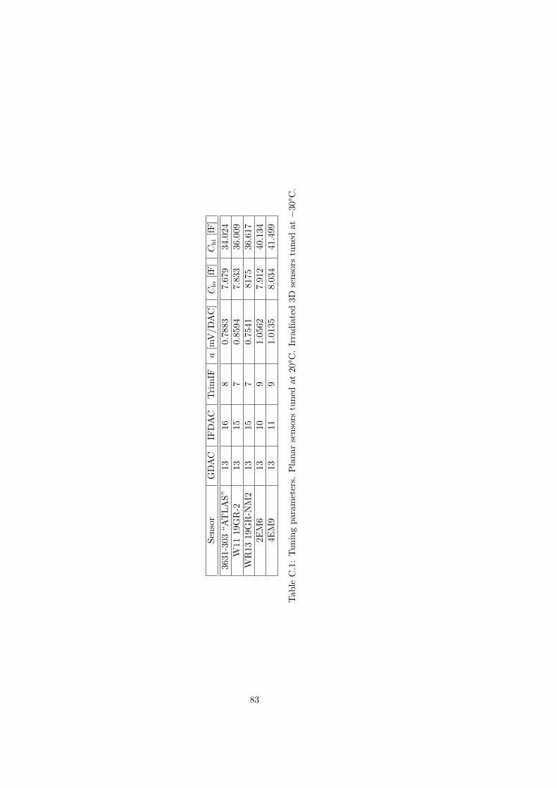
Sens
orG
DA
CIF
DA
CTr
imIF
a[m
V/D
AC
]C
lo
[fF]
C
hi
[fF]
3631
-303
“AT
LAS”
1316
80.
7883
7.67
934
.024
W11
19G
R-2
1315
70.
8594
7.83
336
.009
WR
1319
GR
-NM
213
157
0.75
4181
7536
.617
2EM
613
109
1.05
627.
912
40.1
344E
M9
1311
91.
0135
8.03
441
.499
Tabl
eC
.1:
Tuni
ngpa
ram
eter
s.Pl
anar
sens
ors
tune
dat
20°C
.Ir
radi
ated
3Dse
nsor
stu
ned
at≠
30°C
.
83
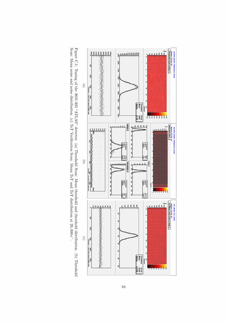
SCU
RVE_M
EAN
: THR
ESHO
LD_SC
AN
.
Module "A
TLAS_7A
"
Colum
n0
24
68
1012
1416
Row
0 20 40 60 80100
120140
3000
3050
3100
3150
3200
3250
3300
3350
3400
Threshold mod 0 chip 0
Constant
210.8M
ean 3208
Sigma
21.49
30003050
31003150
32003250
33003350
3400
20 40 60 80100120140160180200220
Constant
210.8M
ean 3208
Sigma
21.49
"Channel" = row
+160*column+2880*chip
0500
10001500
20002500
30003050310031503200
3250330033503400
(a)
SCU
RVE_SIG
MA
: THR
ESHO
LD_SC
AN
.
Module "A
TLAS_7A
"
Colum
n0
24
68
1012
1416
Row
0 20 40 60 80100120140
150
200
250
300
350
400
450
500
Noise m
od 0 chip 0
Constant
466.9M
ean 180
Sigma
7.287
150200
250300
350400
450500
100
200
300
400
500C
onstant 466.9
Mean
180Sigm
a 7.287
Constant
111.7M
ean 221.6
Sigma
7.563
150200
250300
350400
450500
20 40 60 80
100C
onstant 111.7
Mean
221.6Sigm
a 7.563
long
Constant
13.26M
ean 375.8
Sigma
22.99
150200
250300
350400
450500
2 4 6 8 10 12 14C
onstant 13.26
Mean
375.8Sigm
a 22.99
gangedC
onstant 18.38
Mean
206Sigm
a 13.04
150200
250300
350400
450500
2 4 6 8 10 12 14 16 18 20C
onstant 18.38
Mean
206Sigm
a 13.04
inter-ganged
"Channel" = row
+160*column+2880*chip
0500
10001500
20002500
150
200250
300
350400
450500
(b)
TOT_M
EAN
: TOT_VER
IF.
Module "A
TLAS_7A
"
Colum
n0
24
68
1012
1416
Row
0 20 40 60 80100
120140
24 26 28 30 32 34 36 38
ToTMean m
od 0 bin 0 chip 0
Constant
314.6M
ean 29.86
Sigma
0.5708
2426
2830
3234
3638
50
100
150
200
250
300
Constant
314.6M
ean 29.86
Sigma
0.5708
"Channel" = row
+160*column+2880*chip
0500
10001500
20002500
24 26 28 30 32 34 36 38
(c)
FigureC
.1:Tuning
ofthe3631-303
“ATLA
S”detector.
(a)T
hresholdScan:
Mean
thresholdand
thresholddistribution.
(b)T
hresholdScan:
Mean
noiseand
noisedistribution.
(c)ToT
VerificationScan:
Mean
ToTand
ToTdistribution
at20
,000e ≠.
84
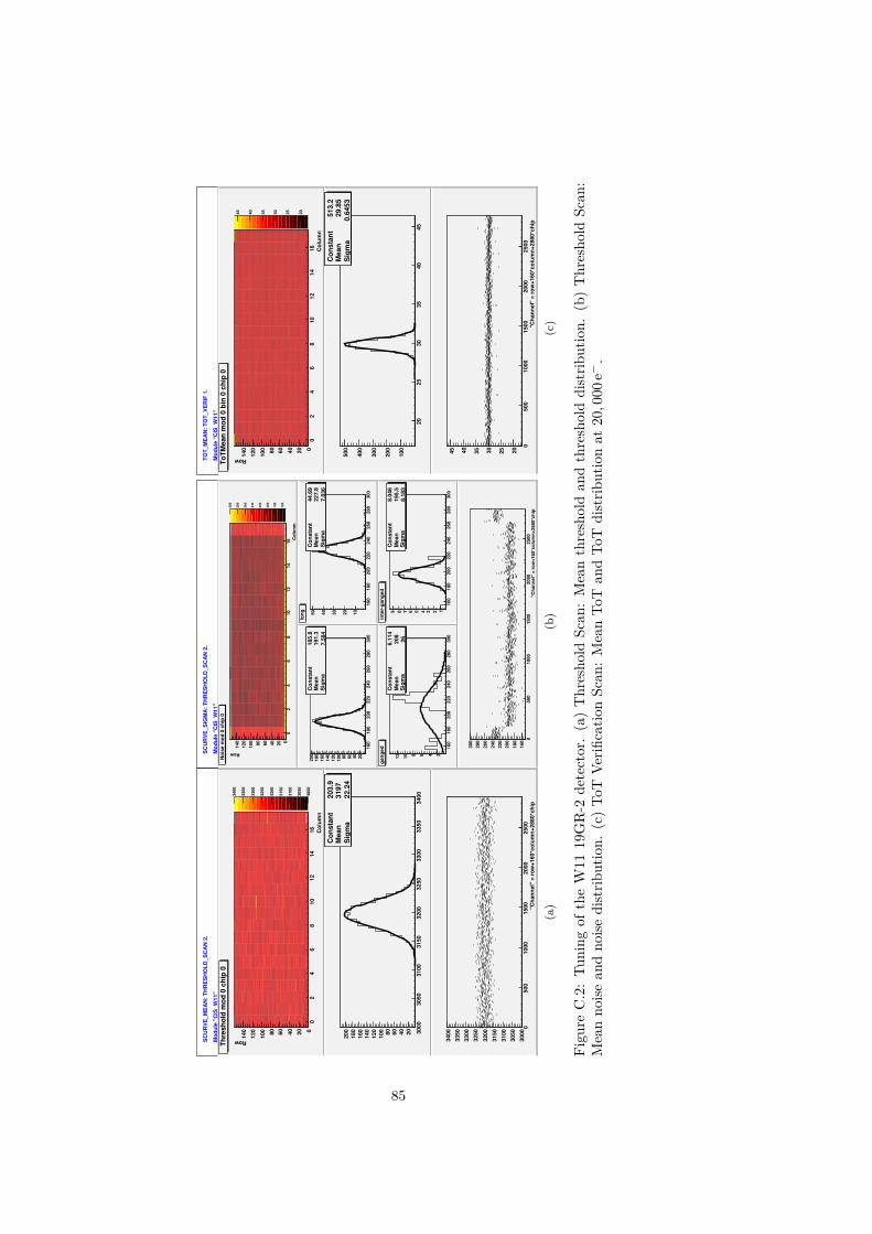
SCU
RVE
_MEA
N: T
HR
ESH
OLD
_SC
AN
2.
Mod
ule
"CIS
_W11
"
Col
umn
02
46
810
1214
16
Row
020406080100
120
140
3000
3050
3100
3150
3200
3250
3300
3350
3400
Thre
shol
d m
od 0
chi
p 0
Con
stan
t 20
3.9
Mea
n 31
97Si
gma
22.2
4
3000
3050
3100
3150
3200
3250
3300
3350
3400
20406080100
120
140
160
180
200
Con
stan
t 20
3.9
Mea
n 31
97Si
gma
22.2
4
"Cha
nnel
" =
row
+160
*col
umn+
2880
*chi
p0
500
1000
1500
2000
2500
3000
3050
3100
3150
3200
3250
3300
3350
3400
(a)
SCU
RVE
_SIG
MA
: TH
RES
HO
LD_S
CA
N 2
.
Mod
ule
"CIS
_W11
"
Col
umn
02
46
810
1214
16
Row
020406080100
120
140
160
180
200
220
240
260
280
300
Noi
se m
od 0
chi
p 0
Con
stan
t 18
5.8
Mea
n 19
1.3
Sigm
a 7.
584
160
180
200
220
240
260
280
300
20406080100
120
140
160
180
200
Con
stan
t 18
5.8
Mea
n 19
1.3
Sigm
a 7.
584
Con
stan
t 44
.69
Mea
n 22
7.8
Sigm
a 7.
836
160
180
200
220
240
260
280
300
1020304050C
onst
ant
44.6
9M
ean
227.
8Si
gma
7.83
6
long
Con
stan
t 6.
114
Mea
n 20
8Si
gma
26
160
180
200
220
240
260
280
300
24681012C
onst
ant
6.11
4M
ean
208
Sigm
a 26
gang
edC
onst
ant
8.04
6M
ean
195.
5Si
gma
8.18
3
160
180
200
220
240
260
280
300
123456789C
onst
ant
8.04
6M
ean
195.
5Si
gma
8.18
3
inte
r-ga
nged "C
hann
el"
= ro
w+1
60*c
olum
n+28
80*c
hip
050
010
0015
0020
0025
0016
018
020
022
024
026
028
030
0
(b)
TOT_
MEA
N: T
OT_
VER
IF 1
.
Mod
ule
"CIS
_W11
"
Col
umn
02
46
810
1214
16
Row
020406080100
120
140
202530354045
ToTM
ean
mod
0 b
in 0
chi
p 0
Con
stan
t 51
3.2
Mea
n 29
.85
Sigm
a 0.
6453
2025
3035
4045
100
200
300
400
500
Con
stan
t 51
3.2
Mea
n 29
.85
Sigm
a 0.
6453
"Cha
nnel
" =
row
+160
*col
umn+
2880
*chi
p0
500
1000
1500
2000
2500
202530354045
(c)
Figu
reC
.2:
Tuni
ngof
the
W11
19G
R-2
dete
ctor
.(a
)T
hres
hold
Scan
:M
ean
thre
shol
dan
dth
resh
old
dist
ribut
ion.
(b)
Thr
esho
ldSc
an:
Mea
nno
isean
dno
isedi
strib
utio
n.(c
)To
TVe
rifica
tion
Scan
:M
ean
ToT
and
ToT
dist
ribut
ion
at20
,00
0e≠
.
85
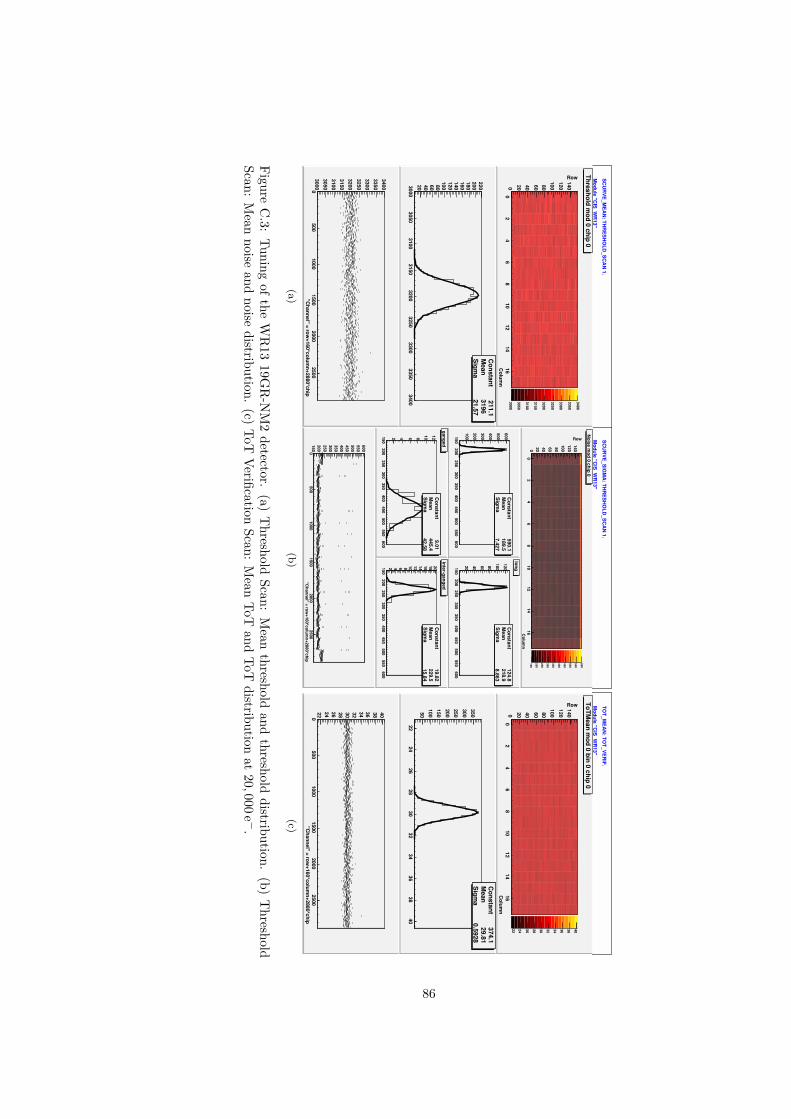
SCU
RVE_M
EAN
: THR
ESHO
LD_SC
AN
1.
Module "C
IS_WR
13"
Colum
n0
24
68
1012
1416
Row
0 20 40 60 80100
120140
3000
3050
3100
3150
3200
3250
3300
3350
3400
Threshold mod 0 chip 0
Constant
211.1M
ean 3196
Sigma
21.57
30003050
31003150
32003250
33003350
3400
20 40 60 80100120140160180200220
Constant
211.1M
ean 3196
Sigma
21.57
"Channel" = row
+160*column+2880*chip
0500
10001500
20002500
30003050310031503200
3250330033503400
(a)
SCU
RVE_SIG
MA
: THR
ESHO
LD_SC
AN
1.
Module "C
IS_WR
13"
Colum
n0
24
68
1012
1416
Row
0 20 40 60 80100120140
150
200
250
300
350
400
450
500
550
600
Noise m
od 0 chip 0
Constant
590.1M
ean 189.5
Sigma
7.427
150200
250300
350400
450500
550600
100
200
300
400
500
600C
onstant 590.1
Mean
189.5Sigm
a 7.427
Constant
124.8M
ean 218.9
Sigma
8.863
150200
250300
350400
450500
550600
20 40 60 80
100
120C
onstant 124.8
Mean
218.9Sigm
a 8.863
long
Constant
9.01M
ean 445.4
Sigma
42.58
150200
250300
350400
450500
550600
2 4 6 8 10 12C
onstant 9.01
Mean
445.4Sigm
a 42.58
gangedC
onstant 19.82
Mean
229.5Sigm
a 15.84
150200
250300
350400
450500
550600
2 4 6 8 10 12 14 16 18 20C
onstant 19.82
Mean
229.5Sigm
a 15.84
inter-ganged
"Channel" = row
+160*column+2880*chip
0500
10001500
20002500
150200250300350400450500550600
(b)
TOT_M
EAN
: TOT_VER
IF.
Module "C
IS_WR
13"
Colum
n0
24
68
1012
1416
Row
0 20 40 60 80100
120140
22 24 26 28 30 32 34 36 38 40
ToTMean m
od 0 bin 0 chip 0
Constant
374.1M
ean 29.81
Sigma
0.5928
2224
2628
3032
3436
3840
50100150
200250
300350
Constant
374.1M
ean 29.81
Sigma
0.5928
"Channel" = row
+160*column+2880*chip
0500
10001500
20002500
22 24 26 28 30 32 34 36 38 40
(c)
FigureC
.3:Tuning
oftheW
R13
19GR
-NM
2detector.
(a)T
hresholdScan:
Mean
thresholdand
thresholddistribution.
(b)T
hresholdScan:
Mean
noiseand
noisedistribution.
(c)ToT
VerificationScan:
Mean
ToTand
ToTdistribution
at20
,000e ≠.
86
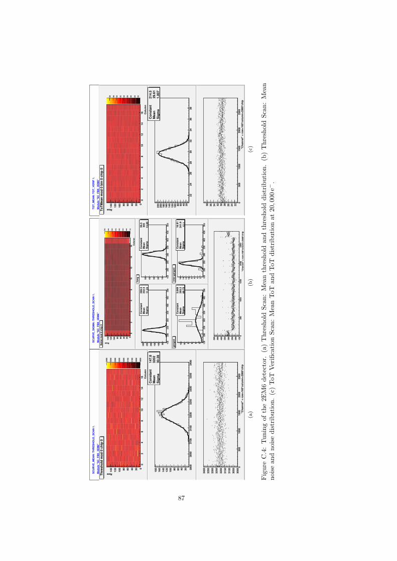
SCU
RVE
_MEA
N: T
HR
ESH
OLD
_SC
AN
1.
Mod
ule
"SC
_FB
K_2
EM6"
Col
umn
02
46
810
1214
16
Row
020406080100
120
140
3000
3050
3100
3150
3200
3250
3300
3350
3400
Thre
shol
d m
od 0
chi
p 0
Con
stan
t 14
7.8
Mea
n 32
02Si
gma
30.2
8
3000
3050
3100
3150
3200
3250
3300
3350
3400
20406080100
120
140
160
180
Con
stan
t 14
7.8
Mea
n 32
02Si
gma
30.2
8
"Cha
nnel
" =
row
+160
*col
umn+
2880
*chi
p0
500
1000
1500
2000
2500
3000
3050
3100
3150
3200
3250
3300
3350
3400
(a)
SCU
RVE
_SIG
MA
: TH
RES
HO
LD_S
CA
N 1
.
Mod
ule
"SC
_FB
K_2
EM6"
Col
umn
02
46
810
1214
16
Row
020406080100
120
140
150
200
250
300
350
400
450
500
Noi
se m
od 0
chi
p 0
Con
stan
t 29
9.5
Mea
n 23
2.5
Sigm
a 11
.24
150
200
250
300
350
400
450
500
50100
150
200
250
300
Con
stan
t 29
9.5
Mea
n 23
2.5
Sigm
a 11
.24
Con
stan
t 56
.5M
ean
303
Sigm
a 13
.85
150
200
250
300
350
400
450
500
1020304050
Con
stan
t 56
.5M
ean
303
Sigm
a 13
.85
long
Con
stan
t 3.
849
Mea
n 29
3.2
Sigm
a 69
.73
150
200
250
300
350
400
450
500
24681012C
onst
ant
3.84
9M
ean
293.
2Si
gma
69.7
3
gang
edC
onst
ant
16.9
1M
ean
241.
9Si
gma
12.1
150
200
250
300
350
400
450
500
246810121416C
onst
ant
16.9
1M
ean
241.
9Si
gma
12.1
inte
r-ga
nged "C
hann
el"
= ro
w+1
60*c
olum
n+28
80*c
hip
050
010
0015
0020
0025
0015
0
200
250
300
350
400
450
500
(b)
TOT_
MEA
N: T
OT_
VER
IF 1
.
Mod
ule
"SC
_FB
K_2
EM6"
Col
umn
02
46
810
1214
16
Row
020406080100
120
140
222426283032343638
ToTM
ean
mod
0 b
in 0
chi
p 0
Con
stan
t 21
4.5
Mea
n 29
.61
Sigm
a 1.
007
2224
2628
3032
3436
3820406080100
120
140
160
180
200
220
Con
stan
t 21
4.5
Mea
n 29
.61
Sigm
a 1.
007
"Cha
nnel
" =
row
+160
*col
umn+
2880
*chi
p0
500
1000
1500
2000
2500
222426283032343638
(c)
Figu
reC
.4:
Tuni
ngof
the
2EM
6de
tect
or.
(a)
Thr
esho
ldSc
an:
Mea
nth
resh
old
and
thre
shol
ddi
strib
utio
n.(b
)T
hres
hold
Scan
:M
ean
noise
and
noise
dist
ribut
ion.
(c)
ToT
Verifi
catio
nSc
an:
Mea
nTo
Tan
dTo
Tdi
strib
utio
nat
20,00
0e≠
.
87
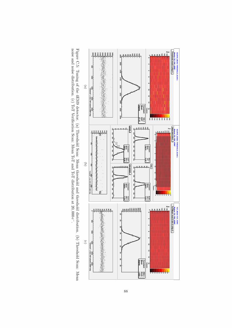
SCU
RVE_M
EAN
: THR
ESHO
LD_SC
AN
2.
Module "SC
_FBK
_4EM9"
Colum
n0
24
68
1012
1416
Row
0 20 40 60 80100
120140
3000
3050
3100
3150
3200
3250
3300
3350
3400
Threshold mod 0 chip 0
Constant
163.1M
ean 3207
Sigma
27.41
30003050
31003150
32003250
33003350
3400
20 40 60 80100120140160
Constant
163.1M
ean 3207
Sigma
27.41
"Channel" = row
+160*column+2880*chip
0500
10001500
20002500
30003050310031503200
3250330033503400
(a)
SCU
RVE_SIG
MA
: THR
ESHO
LD_SC
AN
2.
Module "SC
_FBK
_4EM9"
Colum
n0
24
68
1012
1416
Row
0 20 40 60 80100120140
150
200
250
300
350
400
450
500
Noise m
od 0 chip 0
Constant
304.3M
ean 257
Sigma
10.92
150200
250300
350400
450500
50
100
150
200
250
300C
onstant 304.3
Mean
257Sigm
a 10.92
Constant
55.86M
ean 342.1
Sigma
13.04
150200
250300
350400
450500
10 20 30 40 50
Constant
55.86M
ean 342.1
Sigma
13.04
long
Constant
8.877M
ean 394.6
Sigma
25.88
150200
250300
350400
450500
2 4 6 8 10C
onstant 8.877
Mean
394.6Sigm
a 25.88
gangedC
onstant 18.44
Mean
258.7Sigm
a 11.53
150200
250300
350400
450500
2 4 6 8 10 12 14 16 18C
onstant 18.44
Mean
258.7Sigm
a 11.53
inter-ganged
"Channel" = row
+160*column+2880*chip
0500
10001500
20002500
150
200250
300
350400
450500
(b)
TOT_M
EAN
: TOT_VER
IF.
Module "SC
_FBK
_4EM9"
Colum
n0
24
68
1012
1416
Row
0 20 40 60 80100
120140
22 24 26 28 30 32 34 36 38
ToTMean m
od 0 bin 0 chip 0
Constant
208.3M
ean 29.63
Sigma
1.022
2224
2628
3032
3436
38
20 40 60 80100120140160180200220
Constant
208.3M
ean 29.63
Sigma
1.022
"Channel" = row
+160*column+2880*chip
0500
10001500
20002500
22 24 26 28 30 32 34 36 38
(c)
FigureC
.5:Tuning
ofthe4EM
9detector.
(a)T
hresholdScan:
Mean
thresholdand
thresholddistribution.
(b)T
hresholdScan:
Mean
noiseand
noisedistribution.
(c)ToT
VerificationScan:
Mean
ToTand
ToTdistribution
at20
,000e ≠.
88

Bibliography
[1] Brüning, O.S. et al.: LHC Design Report Volume II — The LHCInfrastructure and General Services. CERN, Geneva, 2004.
[2] The ATLAS Collaboration: ATLAS detector and physics performance:Technical Design Report, Volume 1 . 1999. CERN-LHCC-99-14.
[3] Aad, G. et al.: The ATLAS experiment at the CERN large hadron collider.Journal of Instrumentation, 3:S08003, 2008.
[4] Strandberg, S.: Results from the commissioning of the ATLAS Pixel de-tector. Journal of Instrumentation, 4(03):P03020, 2009. http://stacks.iop.org/1748-0221/4/i=03/a=P03020.
[5] The ATLAS Collaboration: ATLAS Pixel Detector: Technical Design Re-port. 1998. CERN-LHCC-98-13.
[6] Aad, G. et al.: ATLAS pixel detector electronics and sensors. Journal of In-strumentation, 3(07):P07007, 2008. http://stacks.iop.org/1748-0221/3/i=07/a=P07007.
[7] Dobos, D.: Commissioning Perspectives for the ATLAS Pixel Detector.PhD Thesis, University of Dortmund, Dortmund, Sept. 2007.
[8] Rossi, L. et al. (eds.): Pixel Detectors — From Fundamentals to Applica-tions. Springer-Verlag, Heidelberg, 2006, ISBN 3-540-28332-3.
[9] Szczygiel, R.: A state of the art rad-hard digital ASIC design for high energyphysics experiments. Measurement Science and Technology, 18(8):2413,2007. http://stacks.iop.org/0957-0233/18/i=8/a=016.
[10] Anelli, G. et al.: Radiation Tolerant VLSI Circuits in Standard Deep Sub-micron CMOS Technologies for the LHC Experiments: Practical DesignAspects. Nuclear Science, IEEE Transactions on, 46(6):1690–1696, Dec.1999, ISSN 0018-9499. DOI 10.1109/23.819140.
[11] PeriÊ, I.: Design and Realisation of Integrated Circuits for the Readout ofPixel Sensors in High-Energy Physics and Biomedical Imaging. PhD The-sis, University of Bonn, Bonn, Aug. 2004.
[12] Einsweiler, K.: ATLAS Pixel FE Chip: Description and Failure Summary,Dec. 2003. http://pixdata.lbl.gov/html/docs/ATLASPixelFEChip_v3_0.pdf, visited on 14 Oct. 2010.
89
[13] Peric, I. et al.: The FEI3 readout chip for the ATLAS pixel detector. NuclearInstruments and Methods in Physics Research Section A: Accelerators,Spectrometers, Detectors and Associated Equipment, 565(1):178–187,2006, ISSN 0168-9002. http://www.sciencedirect.com/science/article/B6TJM-4K3CY3J-5/2/bc39d9782e35df5fb1076dc06584c623,Proceedings of the International Workshop on Semiconductor PixelDetectors for Particles and Imaging - PIXEL 2005.
[14] Arutinov, D. et al.: Digital architecture and interface of the new ATLASPixel Front-End IC for upgraded LHC luminosity. In Nuclear Science Sym-posium Conference Record, 2008. NSS ’08. IEEE, pp. 1923–1928, Oct. 2008.DOI 10.1109/NSSMIC.2008.4774765.
[15] Karagounis, M. et al.: Development of the ATLAS FE-I4 pixel readoutIC for b-layer Upgrade and Super-LHC. 2008. http://cdsweb.cern.ch/record/1158505, visited on 15 Dec. 2010.
[16] Mathes, M. et al.: Characterization of a single crystal diamond pixeldetector in a high energy particle beam. Journal of Instrumenta-tion, 3(12):P12002, 2008. http://stacks.iop.org/1748-0221/3/i=12/a=P12002.
[17] Nakamura, K. et al.: Review of Particle Physics, 2010–2011. Review ofParticle Properties. J. Phys. G, 37(7A):075021, 2010. http://pdg.lbl.gov.
[18] Mathes, M.: Development and Characterization of Diamond and 3D-SiliconPixel Detectors with ATLAS-Pixel Readout Electronics. PhD Thesis, Uni-versity of Bonn, Bonn, Dec. 2008.
[19] Groom, D.E., Mokhov, N.V., and Striganov, S.I.: Muon Stopping Powerand Range Tables 10MeV–100TeV. Atomic Data and Nuclear Data Tables,78(2):183–356, 2001, ISSN 0092-640X. http://www.sciencedirect.com/science/article/pii/S0092640X01908617.
[20] Landau, L.D.: On the energy loss of particles by ionization. J. Exp.Phys.(USSR), 8:201–205, 1944.
[21] Bichsel, H.: Straggling in thin silicon detectors. Rev. Mod. Phys., 60(3):663–699, Jul 1988. DOI 10.1103/RevModPhys.60.663.
[22] Lutz, G. (ed.): Semiconductors Radiation Detectors. Springer-Verlag, Hei-delberg, 2007, ISBN 978-3-540-71678-5.
[23] Ramo, S.: Currents Induced by Electron Motion. Proceedings of the IRE,27(9):584–585, 1939, ISSN 0096-8390. DOI 10.1109/JRPROC.1939.228757.
[24] Jun, I. et al.: Proton nonionizing energy loss (NIEL) for device applica-tions. IEEE Transactions on Nuclear Science, 50(6):1924–1928, Dec. 2003,ISSN 0018-9499. DOI 10.1109/TNS.2003.820760.
[25] Wunstorf, R.: Systematische Untersuchungen zur Strahlenresistenzvon Silizium-Detektoren für die Verwendung in Hochenergiephysik-Experimenten. PhD thesis, University of Hamburg, Hamburg, 1992. http://books.google.de/books?id=XmTlSgAACAAJ.
90
[26] Lindström, G. et al.: Radiation hard silicon detectors–developmentsby the RD48 (ROSE) collaboration. Nuclear Instruments andMethods in Physics Research Section A: Accelerators, Spectrome-ters, Detectors and Associated Equipment, 466(2):308–326, 2001,ISSN 0168-9002. http://www.sciencedirect.com/science/article/B6TJM-43CK059-F/2/0380b762a87258cfe9e69c45098e53ca, DOI10.1016/S0168-9002(01)00560-5.
[27] Capeans, M. et al.: Atlas insertable b-layer technical design report. Tech.Rep. CERN-LHCC-2010-013. ATLAS-TDR-019, CERN, Geneva, Sept.2010.
[28] Da Via, C. et al.: Advances in silicon detectors for particle track-ing in extreme radiation environments. Nuclear Instruments andMethods in Physics Research Section A: Accelerators, Spectrome-ters, Detectors and Associated Equipment, 509(1–3):86–91, 2003,ISSN 0168-9002. http://www.sciencedirect.com/science/article/B6TJM-48R1NFT-9/2/e861edbfa4bcd1cee9a87375cc819433, DOI10.1016/S0168-9002(03)01554-7".
[29] Hügging, F.G.: Der ATLAS Pixelsensor: Der state-of-the-art Pixelsen-sor für teilchenphysikalische Anwendungen mit extrem hohen Strahlungs-feldern. PhD Thesis, University of Dortmund, Dortmund, June 2001.
[30] Benoit, M., Lounis, A., and Dinu, N.: Simulation of Radiation DamageE�ects on Planar Pixel Guard Ring Structure for ATLAS Inner DetectorUpgrade. Nuclear Science, IEEE Transactions on, 56(6):3236–3243, Dec.2009, ISSN 0018-9499. DOI 10.1109/TNS.2009.2034002.
[31] Beimforde, M.: The ATLAS Planar Pixel Sensor R&D project. Nu-clear Instruments and Methods in Physics Research Section A:Accelerators, Spectrometers, Detectors and Associated Equipment,2010, ISSN 0168-9002. http://www.sciencedirect.com/science/article/B6TJM-4YYGGSV-7/2/69a1b88494d7445642f1e59a59590708,DOI 10.1016/j.nima.2010.04.078.
[32] Weigell, P. et al.: Characterization and Performance of Silicon n-in-p PixelDetectors for the ATLAS Upgrades. Arxiv preprint arXiv:1012.3595, 2010.
[33] Krüger, H.: Test Systems for ATLAS Pixel Detector Upgrade Activities,Jan. 2008. http://icwiki.physik.uni-bonn.de/twiki/pub/Systems/WebHome/ATLAS_Pixel_Chip_Test_Systems.pdf, visited on 30 Dec. 2010.
[34] Backhaus, M.: Development of an USB-based test system for the FE-I3readout chips of the ATLAS pixel detector and Noise Occupancy Studies.Diploma Thesis, University of Bonn, Bonn, Dec. 2009.
[35] Schneider, J. and Krüger, H.: S3 Multi IO System, Jan. 2010. http://icwiki.physik.uni-bonn.de/svn/USBpixI4/doc/MultiIOboard_V1.03_Manual.pdf, visited on 18 Nov. 2010.
[36] Köhler, F.: Threshold di�erence USBpix – TurboDAQ, Jan. 2010. http://indico.cern.ch/event/80615, visited on 14 Oct. 2010.
91
[37] Backhaus, M. et al.: Development of a versatile and modular test systemfor ATLAS hybrid pixel detectors. Nuclear Instruments and Methods inPhysics Research Section A: Accelerators, Spectrometers, Detectors andAssociated Equipment, 2010. DOI 10.1016/j.nima.2010.12.087.
[38] EUDET JRA1 Group: Mechanics of the EUDET JRA1 telescope. http://www.desy.de/~gregor/EUDET/Mechanics/CERN_Aufbau2.pdf, visited on16 Oct. 2010.
[39] Baudot, J. et al.: First test results of MIMOSA-26, a fast CMOS sensorwith integrated zero suppression and digitized output. Nuclear Science Sym-posium Conference Record (NSS/MIC), 2009 IEEE, pp. 1169–1173, Oct.2009, ISSN 1082-3654. DOI 10.1109/NSSMIC.2009.5402399.
[40] Cussans, D.: Description of the JRA1 Trigger Logic Unit (TLU),v0.2c, Sept. 2009. http://www.eudet.org/e26/e28/e42441/e57298/EUDET-MEMO-2009-04.pdf, visited on 14 Oct. 2010.
[41] Schultes, S.: Entwicklung eines Strahl-Teleskops mit ATLAS-Pixeldetektoren. Diploma Thesis, University of Bonn, Bonn, July2011.
[42] Hügging, F. Private communication, Dec. 2010.
[43] Köhler, M.: Studies of the Timing Behaviour of the ATLAS Pixel Detector.Master Thesis, University of of Siegen, Siegen, Aug. 2008.
[44] Chen, J., Sylvester, D., and Hu, C.: An on-chip, interconnect capac-itance characterization method with sub-femto-farad resolution. IEEETransactions on Semiconductor Manufacturing, 11(2):204–210, May 1998,ISSN 0894-6507. DOI 10.1109/66.670160.
[45] Behara, P. et al.: Threshold Tuning of the ATLAS Pixel Detector. Tech.Rep. ATL-INDET-PUB-2010-001, CERN, Geneva, Aug. 2010. http://cdsweb.cern.ch/record/1283928, visited on 18 Nov. 2010.
[46] Große-Knetter, J.: Vertex Measurements at a Hadron Collider — TheATLAS Pixel Detector. Habilitation Thesis, University of Bonn, Bonn,Mar. 2008.
[47] Andreazza, A.: Test beam performance of the ATLAS Pixel Detector mod-ules. Nuclear Instruments and Methods in Physics Research Section A: Ac-celerators, Spectrometers, Detectors and Associated Equipment, 565(1):23–29, 2006, ISSN 0168-9002. http://www.sciencedirect.com/science/article/B6TJM-4K5J9HH-3/2/a3ecf43b5e5811b4926f14638fcaa99f,DOI 10.1016/j.nima.2006.04.095.
[48] Dalla Betta, G.F. et al.: Development of 3D-DDTC pixel detec-tors for the ATLAS upgrade. Nuclear Instruments and Methodsin Physics Research Section A: Accelerators, Spectrometers, De-tectors and Associated Equipment, 2010, ISSN 70168-9002. http://www.sciencedirect.com/science/article/B6TJM-4YYGGSV-8/2/ea5307c6c1b214b9835d1aa11cd068fc, DOI 10.1016/j.nima.2010.04.079.
92

[49] La Rosa, A.: Measurements of 3D/FBK sensors, Nov. 2009. http://indico.cern.ch/event/65918, visited on 25 Dec. 2010, RD50 Work-shop.
93


