Embed Size (px)
Citation preview
Good Display
E paper IC Specifications SPEC NO
IL3829 REV NO
Good Display Specifications
Prepared: AiMing Wei Checked: YongCheng Jian Approved: Boris Ren Issue Date: 2016.4.7
Dalian Good Display Co., Ltd. Good Display
No.17 Gonghua Street, Shahekou District, Dalian 116021 China Tel: +86-411-84619565 Fax: +86-411-84619585
E-mail: [email protected] Website: www.good-display.com
CONTENTS
1 GENERAL DESCRIPTION ....................................................................................................... 6
2 FEATURES................................................................................................................................... 6
3 ORDERING INFORMATION ................................................................................................... 7
4 BLOCK DIAGRAM .................................................................................................................... 7
5 DIE PAD FLOOR PLAN ............................................................................................................ 8
6 PIN DESCRIPTION .................................................................................................................. 12
7 FUNCTIONAL BLOCK DESCRIPTION............................................................................... 16 7.1 MCU INTERFACE.................................................................................................................................................16
7.1.1 MCU Interface selection .............................................................................................................................16 7.1.2 MCU 6800-series Parallel Interface...........................................................................................................16 7.1.3 MCU 8080-series Parallel Interface...........................................................................................................17 7.1.4 MCU Serial Peripheral Interface (4-wire SPI)...........................................................................................20 7.1.5 MCU Serial Peripheral Interface (3-wire SPI)...........................................................................................21
7.2 RAM ...................................................................................................................................................................22 7.3 OSCILLATOR........................................................................................................................................................22 7.4 BOOSTER & REGULATOR.....................................................................................................................................23 7.5 PANEL DRIVING WAVEFORM...............................................................................................................................24 7.6 VCOM SENSING..................................................................................................................................................25 7.7 GATE AND PROGRAMMABLE SOURCE WAVEFORM ..............................................................................................25 7.8 WAVEFORM LOOK UP TABLE (LUT)...................................................................................................................26 7.9 OTP.....................................................................................................................................................................26
7.9.1 Temperature Searching Mechanism ...........................................................................................................28 7.10 EXTERNAL TEMPERATURE SENSOR I2C SINGLE MASTER INTERFACE .................................................................29 7.11 CASCADE MODE ..................................................................................................................................................29
8 COMMAND TABLE ................................................................................................................. 30
9 COMMAND DESCRIPTION................................................................................................... 41 9.1 DRIVER OUTPUT CONTROL (01H) ........................................................................................................................41 9.2 GATE SCAN START POSITION (0FH).....................................................................................................................43 9.3 DATA ENTRY MODE SETTING (11H) ....................................................................................................................44 9.4 SET RAM X - ADDRESS START / END POSITION (44H) ........................................................................................45 9.5 SET RAM Y - ADDRESS START / END POSITION (45H) ........................................................................................45 9.6 SET RAM ADDRESS COUNTER (4EH-4FH) ..........................................................................................................45
10 TYPICAL OPERATING SEQUENCE ................................................................................ 46 10.1 NORMAL DISPLAY ...............................................................................................................................................46 10.2 VCOM OTP PROGRAM .......................................................................................................................................47 10.3 WS OTP PROGRAM .............................................................................................................................................48
11 ABSOLUTE MAXIMUM RATING ..................................................................................... 49
12 ELECTRICAL CHARACTERISTICS ................................................................................ 50
13 AC CHARACTERISTICS..................................................................................................... 52 13.1 OSCILLATOR FREQUENCY ....................................................................................................................................52 13.2 INTERFACE TIMING..............................................................................................................................................53
13.2.1 MCU 6800-Series Parallel Interface ..........................................................................................................53 13.2.2 MCU 8080-Series Parallel Interface ..........................................................................................................54 13.2.3 Serial Peripheral Interface .........................................................................................................................55
14 APPLICATION CIRCUIT .................................................................................................... 56
IL3829
Dalian Good Display Co., Ltd.
TABLES TABLE 3-1 : ORDERING INFORMATION .................................................................................................................................7 TABLE 5-1 : IL3829Z BUMP DIE PAD COORDINATES.....................................................................................................9 TABLE 6-1 : MCU INTERFACE SELECTION .........................................................................................................................14 TABLE 7-1 : MCU INTERFACE SELECTION BY BS0 AND BS1 ............................................................................................16 TABLE 7-2 : MCU INTERFACE ASSIGNMENT UNDER DIFFERENT BUS INTERFACE MODE ...................................................16 TABLE 7-3 : CONTROL PINS OF 6800 INTERFACE ..............................................................................................................16 TABLE 7-4 : CONTROL PINS OF 8080 INTERFACE (FORM 1) .............................................................................................18 TABLE 7-5 : CONTROL PINS OF 8080 INTERFACE (FORM 2) .............................................................................................18 TABLE 7-6 : CONTROL PINS OF 4-WIRE SERIAL PERIPHERAL INTERFACE.........................................................................20 TABLE 7-7 : CONTROL PINS OF 3-WIRE SERIAL PERIPHERAL INTERFACE.........................................................................21 TABLE 7-8 : RAM ADDRESS MAP .......................................................................................................................................22 TABLE 8-1: COMMAND TABLE ............................................................................................................................................30 TABLE 11-1: MAXIMUM RATINGS .......................................................................................................................................49 TABLE 12-1: DC CHARACTERISTICS..................................................................................................................................50 TABLE 12-2: REGULATORS CHARACTERISTICS .................................................................................................................51 TABLE 13-1: OSCILLATOR FREQUENCY.............................................................................................................................52 TABLE 13-2 : 6800-SERIES MCU PARALLEL INTERFACE TIMING CHARACTERISTICS .....................................................53 TABLE 13-3 : MCU 8080-SERIES PARALLEL INTERFACE TIMING CHARACTERISTICS .....................................................54 TABLE 13-4 : SERIAL PERIPHERAL INTERFACE TIMING CHARACTERISTICS......................................................................55 TABLE 14-1 : REFERENCE COMPONENT VALUE...................................................................................................................58 FIGURES FIGURE 4-1 : IL3829 BLOCK DIAGRAM...........................................................................................................................7 FIGURE 5-1 - IL3829Z DIE FLOOR PLAN (BUMP FACE UP )............................................................................................8 FIGURE 7-1 : DATA READ BACK PROCEDURE - INSERTION OF DUMMY READ.....................................................................17 FIGURE 7-2 : EXAMPLE OF WRITE PROCEDURE IN 8080 PARALLEL INTERFACE MODE ....................................................17 FIGURE 7-3 : EXAMPLE OF READ PROCEDURE IN 8080 PARALLEL INTERFACE MODE ......................................................18 FIGURE 7-4 : DISPLAY DATA READ BACK PROCEDURE - INSERTION OF DUMMY READ ......................................................19 FIGURE 7-5 : WRITE PROCEDURE IN 4-WIRE SERIAL PERIPHERAL INTERFACE MODE......................................................20 FIGURE 7-6 : WRITE PROCEDURE IN 3-WIRE SERIAL PERIPHERAL INTERFACE MODE......................................................21 FIGURE 7-7 : INPUT AND OUTPUT VOLTAGE RELATION CHART ..........................................................................................23 FIGURE 7-8 : VPIXEL DEFINITION .......................................................................................................................................24 FIGURE 7-9 : THE RELATION OF VPIXEL WAVEFORM WITH GATE AND SOURCE ..............................................................24 FIGURE 7-10 : PROGRAMMABLE SOURCE AND GATE WAVEFORM ILLUSTRATION ............................................................25 FIGURE 7-11 : VS[N-XY] AND TP[N] MAPPING IN LUT......................................................................................................26 FIGURE 7-12 : OTP CONTENT AND ADDRESS MAPPING ..................................................................................................27 FIGURE 7-13 : WAVEFORM SETTING AND TEMPERATURE RANGE # MAPPING .................................................................28 FIGURE 9-1: OUTPUT PIN ASSIGNMENT ON DIFFERENT SCAN MODE SETTING.................................................................42 FIGURE 9-2: EXAMPLE OF SET DISPLAY START LINE WITH NO REMAPPING ....................................................................43 FIGURE 13-1 : MCU 6800-SERIES PARALLEL INTERFACE CHARACTERISTICS..................................................................53 FIGURE 13-2 : 8080-SERIES PARALLEL INTERFACE CHARACTERISTICS (FORM 1) ...........................................................54 FIGURE 13-3 : 8080-SERIES PARALLEL INTERFACE CHARACTERISTICS (FORM 2) ...........................................................54 FIGURE 13-4 : SERIAL PERIPHERAL INTERFACE CHARACTERISTICS .................................................................................55 FIGURE 14-1 : BOOSTER CONNECTION DIAGRAM .............................................................................................................56 FIGURE 14-2 : TYPICAL APPLICATION DIAGRAM WITH SPI INTERFACE ................................................................................57
IL3829
Dalian Good Display Co., Ltd.
1 GENERAL DESCRIPTION
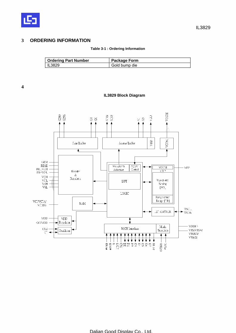
The IL3829 is a CMOS active matrix bistable display driver with controller. It consists of 200 source outputs, 300 gate outputs, 1 VCOM and 1 VBD for border that can support a maximum display resolution 200x300 for single chip application. In addition, the IL3829 has a cascade mode that can support higher display resolution.
The IL3829 embeds booster, regulators and oscillator. Data/Commands are sent from general MCU through the hardware selectable 6800-/8080-series compatible Parallel Interface or Serial Peripheral Interface.
2 FEATURES • Design for dot matrix type active matrix EPD display • Resolution: 200 source outputs; 300 gate outputs; 1 VCOM; 1VBD for border • Power supply
VCI: 2.4 to 3.7V VDDIO: Connect to VCI VDD: 1.8V, regulate from VCI supply
• Gate driving output voltage:
2 levels output (VGH, VGL) Max 42Vp-p VGH: 15V to 22V; VGL: -20V to -15V Voltage adjustment in steps of 500mV.
• Source / VBD driving output voltage:
3 levels output (VSH, VSS, VSL) VSH: 10V to 17V VSL: -10V to -17V Voltage adjustment in steps of 500mV
• VCOM output voltage
-4V to 0.2V in 20mV resolution 8 bits Non-volatile memory (OTP) for VCOM adjustment
• Source and gate scan direction control • Low current deep sleep mode • On chip display RAM with double display buffer [200x300 / 8 * 2 = 15000Byte] • Waveform settings can be programmed and stored in On-chip OTP • Programmable output waveform allowing flexibility for different applications / environments. • Built in VCOM sensing • On-chip oscillator. • On-chip booster and regulator control for generating VCOM, Gate and Source driving
voltage. • Cascade mode to support higher display resolution. • I2C Single Master Interface to read external temperature sensor reading • 8-bits Parallel (6800 & 8080), Serial peripheral interface available • Available in COG package
IL3829
Dalian Good Display Co., Ltd.
3 ORDERING INFORMATION Table 3-1 : Ordering Information
Ordering Part Number Package Form IL3829 Gold bump die
4
IL3829 Block Diagram
IL3829
Dalian Good Display Co., Ltd.
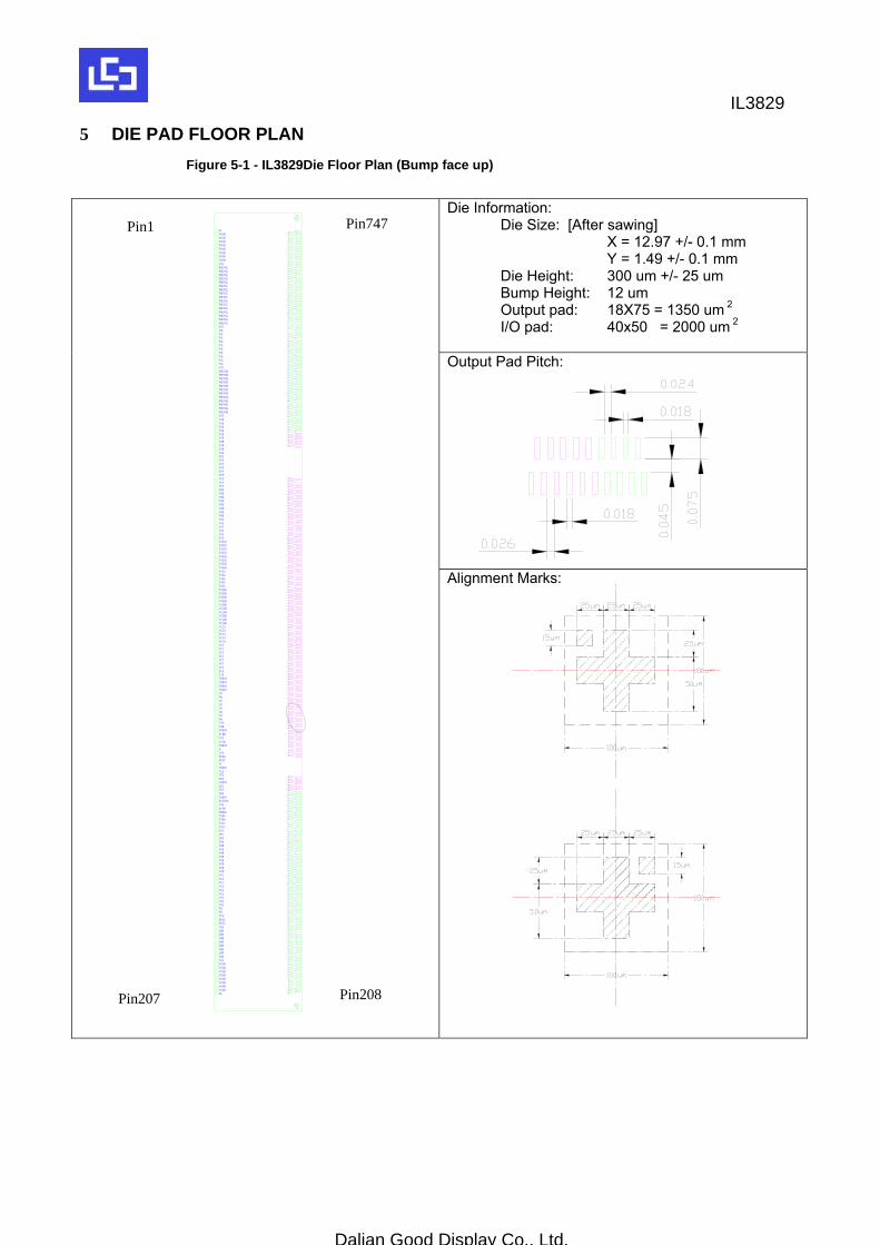
5 DIE PAD FLOOR PLAN Figure 5-1 - IL3829Die Floor Plan (Bump face up)
Die Information: Die Size: [After sawing] X = 12.97 +/- 0.1 mm Y = 1.49 +/- 0.1 mm Die Height: 300 um +/- 25 um Bump Height: 12 um
Output pad: 18X75 = 1350 um 2 I/O pad: 40x50 = 2000 um 2 Output Pad Pitch:
NCVCOMVCOMVCOMVCOMVCOMVCOMVCOMVCOMVSSPREVGLPREVGLPREVGLPREVGLPREVGLPREVGLPREVGLPREVGLPREVGLPREVGLPREVGLPREVGLPREVGLPREVGLPREVGLPREVGLVSSVSLVSLVSLVSLVSLVSLVSLVSLVSLVSLVSSPREVGHPREVGHPREVGHPREVGHPREVGHPREVGHPREVGHPREVGHPREVGHPREVGHPREVGHPREVGHVSSVSHVSHVSHVSHVSHVSHVSHVSHVSHVSHVSSVPPVPPVPPVPPVPPVPPVPPVPPVDDVDDVDDVDDVDDVDDVDDVDDVSSVSSVSSVSSVSSVSSVSSGSVSSGSVSSGSVSSGSVSSGSVSSGSVSSGSVSSGSVSSAVSSAVSSAVSSAVSSAVSSBGVSSBGVSSBGVSSBGVSSBGVCIBGVCIBGVCIBGVCIBGVCIBGVCIAVCIAVCIAVCIAVCIAVCIVCIVCIVCIVCIVCIVCITPETINVDDIOVDDIOVDDIOVDDIOD7D6D5D4D3D2D1D0VSSCS#VDDIOR/W#VSSD/C#VDDIOEVSSRES#BUSYCLVDDIOCLSVSSBS2VDDIOBS1VSSBS0VDDIOEXTVDDVSSM/S#VDDIOTSDATSDATSCLTSCLTPATPCTPDTPBVGHVGHVGHVGHVGHVGHVGHVGHVGLVGLVGLVGLVGLVGLVGLVGLVSSFBFBVSSRESERESEVSSGDRGDRGDRGDRGDRGDRGDRGDRVSSVCOMVCOMVCOMVCOMVCOMVCOMVCOMVCOMNC
NC
G2
G6
G10
G14
G18
G22
G26
G30
G34
G38
G42
G46
G50
G54
G58
G62
G66
G70
G74
G78
G82
G86
G90
G94
G98
G102
G106
G110
G114
G118
G122
G126
G130
G134
G138
G142
G146
G150
G154
G158
G162
G166
G170
G174
G178
G182
G186
G190
G194
G198
G202
G206
G210
G214
G218
G222
G226
G230
G234
G238
G242
G246
G250
G254
G258
G262
G266
G270
G274
G278
G282
G286
G290
G294
G298
NC
VBD
S1
S3
S5
S7
S9
S11
S13
S15
S17
S19
S21
S23
S25
S27
S29
S31
S33
S35
S37
S39
S41
S43
S45
S47
S49
S51
S53
S55
S57
S59
S61
S63
S65
S67
S69
S71
S73
S75
S77
S79
S81
S83
S85
S87
S89
S91
S93
S95
S97
S99
S101
S103
S105
S107
S109
S111
S113
S115
S117
S119
S121
S123
S125
S127
S129
S131
S133
S135
S137
S139
S141
S143
S145
S147
S149
S151
S153
S155
S157
S159
S161
S163
S165
S167
S169
S171
S173
S175
S177
S179
S181
S183
S185
S187
S189
S191
S193
S195
S197
S199
NC
NC
NC
NC
NC
NC
NC
NC
NC
NC
NC
NC
NC
G297
G293
G289
G285
G281
G277
G273
G269
G265
G261
G257
G253
G249
G245
G241
G237
G233
G229
G225
G221
G217
G213
G209
G205
G201
G197
G193
G189
G185
G181
G177
G173
G169
G165
G161
G157
G153
G149
G145
G141
G137
G133
G129
G125
G121
G117
G113
G109
G105
G101
G97
G93
G89
G85
G81
G77
G73
G69
G65
G61
G57
G53
G49
G45
G41
G37
G33
G29
G25
G21
G17
G13
G9
G5
G1
NC
NC
G0
G4
G8
G12
G16
G20
G24
G28
G32
G36
G40
G44
G48
G52
G56
G60
G64
G68
G72
G76
G80
G84
G88
G92
G96
G100
G104
G108
G112
G116
G120
G124
G128
G132
G136
G140
G144
G148
G152
G156
G160
G164
G168
G172
G176
G180
G184
G188
G192
G196
G200
G204
G208
G212
G216
G220
G224
G228
G232
G236
G240
G244
G248
G252
G256
G260
G264
G268
G272
G276
G280
G284
G288
G292
G296
NC
NC
NC
NC
NC
NC
S0
S2
S4
S6
S8
S10
S12
S14
S16
S18
S20
S22
S24
S26
S28
S30
S32
S34
S36
S38
S40
S42
S44
S46
S48
S50
S52
S54
S56
S58
S60
S62
S64
S66
S68
S70
S72
S74
S76
S78
S80
S82
S84
S86
S88
S90
S92
S94
S96
S98
S100
S102
S104
S106
S108
S110
S112
S114
S116
S118
S120
S122
S124
S126
S128
S130
S132
S134
S136
S138
S140
S142
S144
S146
S148
S150
S152
S154
S156
S158
S160
S162
S164
S166
S168
S170
S172
S174
S176
S178
S180
S182
S184
S186
S188
S190
S192
S194
S196
S198
VBD
NC
NC
NC
NC
NC
NC
G299
G295
G291
G287
G283
G279
G275
G271
G267
G263
G259
G255
G251
G247
G243
G239
G235
G231
G227
G223
G219
G215
G211
G207
G203
G199
G195
G191
G187
G183
G179
G175
G171
G167
G163
G159
G155
G151
G147
G143
G139
G135
G131
G127
G123
G119
G115
G111
G107
G103
G99
G95
G91
G87
G83
G79
G75
G71
G67
G63
G59
G55
G51
G47
G43
G39
G35
G31
G27
G23
G19
G15
G11
G7
G3
NC
NCNC
NC
NC
NCNC
NC
NC
Alignment Marks:
Pin1
Pin207 Pin208
Pin747
IL3829
Dalian Good Display Co., Ltd.
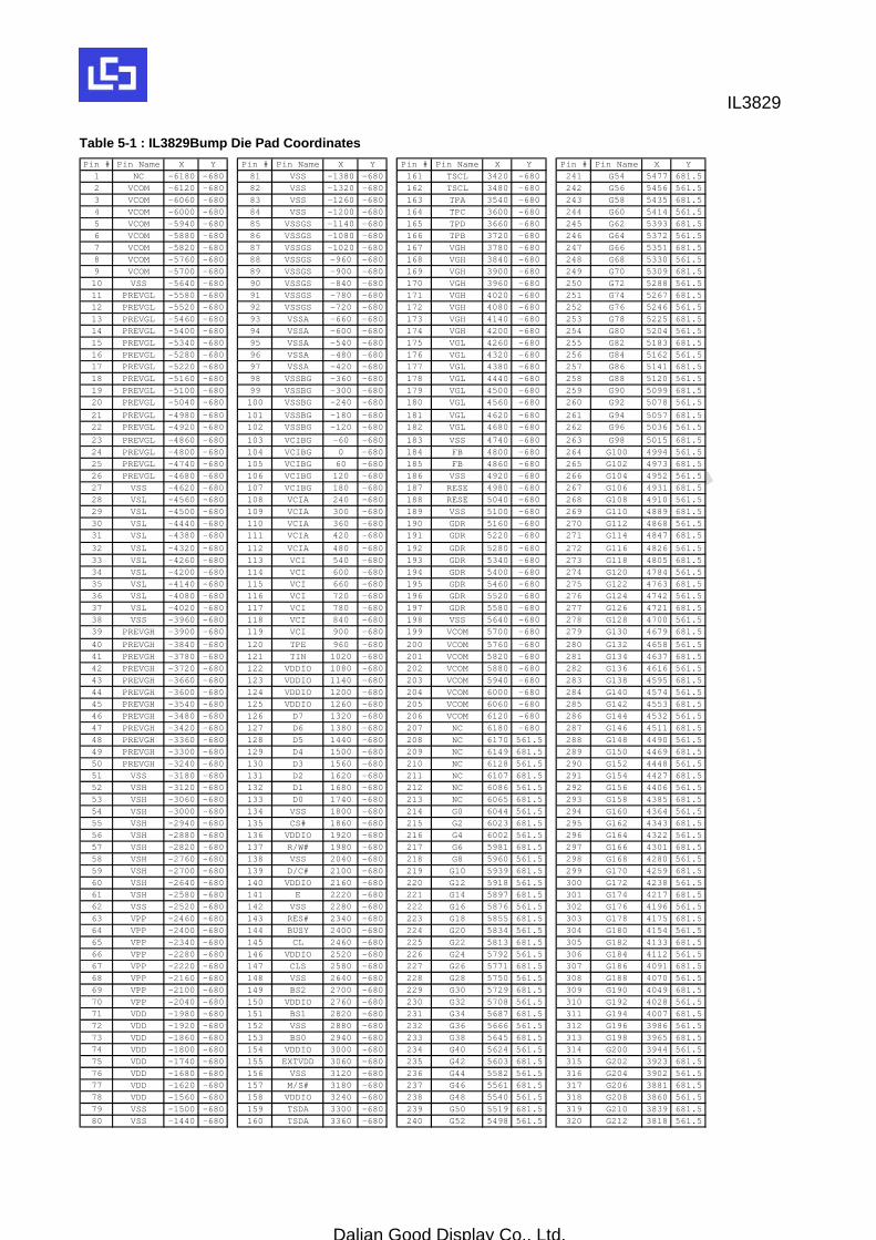
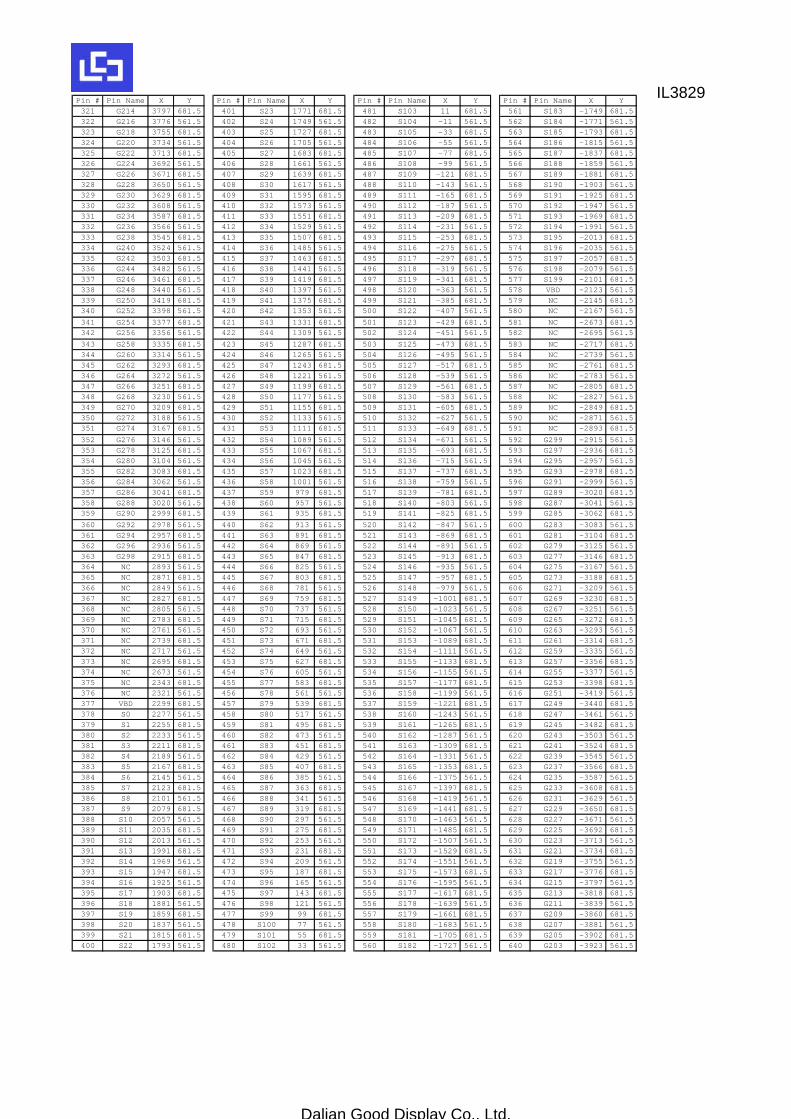
Table 5-1 : IL3829Bump Die Pad Coordinates Pin # Pin Name X Y Pin # Pin Name X Y Pin # Pin Name X Y Pin # Pin Name X Y
1 NC -6180 -680 81 VSS -1380 -680 161 TSCL 3420 -680 241 G54 5477 681.52 VCOM -6120 -680 82 VSS -1320 -680 162 TSCL 3480 -680 242 G56 5456 561.53 VCOM -6060 -680 83 VSS -1260 -680 163 TPA 3540 -680 243 G58 5435 681.54 VCOM -6000 -680 84 VSS -1200 -680 164 TPC 3600 -680 244 G60 5414 561.55 VCOM -5940 -680 85 VSSGS -1140 -680 165 TPD 3660 -680 245 G62 5393 681.56 VCOM -5880 -680 86 VSSGS -1080 -680 166 TPB 3720 -680 246 G64 5372 561.57 VCOM -5820 -680 87 VSSGS -1020 -680 167 VGH 3780 -680 247 G66 5351 681.58 VCOM -5760 -680 88 VSSGS -960 -680 168 VGH 3840 -680 248 G68 5330 561.59 VCOM -5700 -680 89 VSSGS -900 -680 169 VGH 3900 -680 249 G70 5309 681.510 VSS -5640 -680 90 VSSGS -840 -680 170 VGH 3960 -680 250 G72 5288 561.511 PREVGL -5580 -680 91 VSSGS -780 -680 171 VGH 4020 -680 251 G74 5267 681.512 PREVGL -5520 -680 92 VSSGS -720 -680 172 VGH 4080 -680 252 G76 5246 561.513 PREVGL -5460 -680 93 VSSA -660 -680 173 VGH 4140 -680 253 G78 5225 681.514 PREVGL -5400 -680 94 VSSA -600 -680 174 VGH 4200 -680 254 G80 5204 561.515 PREVGL -5340 -680 95 VSSA -540 -680 175 VGL 4260 -680 255 G82 5183 681.516 PREVGL -5280 -680 96 VSSA -480 -680 176 VGL 4320 -680 256 G84 5162 561.517 PREVGL -5220 -680 97 VSSA -420 -680 177 VGL 4380 -680 257 G86 5141 681.518 PREVGL -5160 -680 98 VSSBG -360 -680 178 VGL 4440 -680 258 G88 5120 561.519 PREVGL -5100 -680 99 VSSBG -300 -680 179 VGL 4500 -680 259 G90 5099 681.520 PREVGL -5040 -680 100 VSSBG -240 -680 180 VGL 4560 -680 260 G92 5078 561.5
21 PREVGL -4980 -680 101 VSSBG -180 -680 181 VGL 4620 -680 261 G94 5057 681.522 PREVGL -4920 -680 102 VSSBG -120 -680 182 VGL 4680 -680 262 G96 5036 561.5
23 PREVGL -4860 -680 103 VCIBG -60 -680 183 VSS 4740 -680 263 G98 5015 681.524 PREVGL -4800 -680 104 VCIBG 0 -680 184 FB 4800 -680 264 G100 4994 561.525 PREVGL -4740 -680 105 VCIBG 60 -680 185 FB 4860 -680 265 G102 4973 681.526 PREVGL -4680 -680 106 VCIBG 120 -680 186 VSS 4920 -680 266 G104 4952 561.527 VSS -4620 -680 107 VCIBG 180 -680 187 RESE 4980 -680 267 G106 4931 681.528 VSL -4560 -680 108 VCIA 240 -680 188 RESE 5040 -680 268 G108 4910 561.529 VSL -4500 -680 109 VCIA 300 -680 189 VSS 5100 -680 269 G110 4889 681.530 VSL -4440 -680 110 VCIA 360 -680 190 GDR 5160 -680 270 G112 4868 561.531 VSL -4380 -680 111 VCIA 420 -680 191 GDR 5220 -680 271 G114 4847 681.5
32 VSL -4320 -680 112 VCIA 480 -680 192 GDR 5280 -680 272 G116 4826 561.533 VSL -4260 -680 113 VCI 540 -680 193 GDR 5340 -680 273 G118 4805 681.534 VSL -4200 -680 114 VCI 600 -680 194 GDR 5400 -680 274 G120 4784 561.535 VSL -4140 -680 115 VCI 660 -680 195 GDR 5460 -680 275 G122 4763 681.536 VSL -4080 -680 116 VCI 720 -680 196 GDR 5520 -680 276 G124 4742 561.537 VSL -4020 -680 117 VCI 780 -680 197 GDR 5580 -680 277 G126 4721 681.538 VSS -3960 -680 118 VCI 840 -680 198 VSS 5640 -680 278 G128 4700 561.539 PREVGH -3900 -680 119 VCI 900 -680 199 VCOM 5700 -680 279 G130 4679 681.5
40 PREVGH -3840 -680 120 TPE 960 -680 200 VCOM 5760 -680 280 G132 4658 561.541 PREVGH -3780 -680 121 TIN 1020 -680 201 VCOM 5820 -680 281 G134 4637 681.542 PREVGH -3720 -680 122 VDDIO 1080 -680 202 VCOM 5880 -680 282 G136 4616 561.543 PREVGH -3660 -680 123 VDDIO 1140 -680 203 VCOM 5940 -680 283 G138 4595 681.544 PREVGH -3600 -680 124 VDDIO 1200 -680 204 VCOM 6000 -680 284 G140 4574 561.545 PREVGH -3540 -680 125 VDDIO 1260 -680 205 VCOM 6060 -680 285 G142 4553 681.546 PREVGH -3480 -680 126 D7 1320 -680 206 VCOM 6120 -680 286 G144 4532 561.547 PREVGH -3420 -680 127 D6 1380 -680 207 NC 6180 -680 287 G146 4511 681.548 PREVGH -3360 -680 128 D5 1440 -680 208 NC 6170 561.5 288 G148 4490 561.549 PREVGH -3300 -680 129 D4 1500 -680 209 NC 6149 681.5 289 G150 4469 681.550 PREVGH -3240 -680 130 D3 1560 -680 210 NC 6128 561.5 290 G152 4448 561.551 VSS -3180 -680 131 D2 1620 -680 211 NC 6107 681.5 291 G154 4427 681.552 VSH -3120 -680 132 D1 1680 -680 212 NC 6086 561.5 292 G156 4406 561.553 VSH -3060 -680 133 D0 1740 -680 213 NC 6065 681.5 293 G158 4385 681.554 VSH -3000 -680 134 VSS 1800 -680 214 G0 6044 561.5 294 G160 4364 561.555 VSH -2940 -680 135 CS# 1860 -680 215 G2 6023 681.5 295 G162 4343 681.556 VSH -2880 -680 136 VDDIO 1920 -680 216 G4 6002 561.5 296 G164 4322 561.557 VSH -2820 -680 137 R/W# 1980 -680 217 G6 5981 681.5 297 G166 4301 681.558 VSH -2760 -680 138 VSS 2040 -680 218 G8 5960 561.5 298 G168 4280 561.559 VSH -2700 -680 139 D/C# 2100 -680 219 G10 5939 681.5 299 G170 4259 681.560 VSH -2640 -680 140 VDDIO 2160 -680 220 G12 5918 561.5 300 G172 4238 561.561 VSH -2580 -680 141 E 2220 -680 221 G14 5897 681.5 301 G174 4217 681.562 VSS -2520 -680 142 VSS 2280 -680 222 G16 5876 561.5 302 G176 4196 561.563 VPP -2460 -680 143 RES# 2340 -680 223 G18 5855 681.5 303 G178 4175 681.564 VPP -2400 -680 144 BUSY 2400 -680 224 G20 5834 561.5 304 G180 4154 561.565 VPP -2340 -680 145 CL 2460 -680 225 G22 5813 681.5 305 G182 4133 681.566 VPP -2280 -680 146 VDDIO 2520 -680 226 G24 5792 561.5 306 G184 4112 561.567 VPP -2220 -680 147 CLS 2580 -680 227 G26 5771 681.5 307 G186 4091 681.568 VPP -2160 -680 148 VSS 2640 -680 228 G28 5750 561.5 308 G188 4070 561.569 VPP -2100 -680 149 BS2 2700 -680 229 G30 5729 681.5 309 G190 4049 681.570 VPP -2040 -680 150 VDDIO 2760 -680 230 G32 5708 561.5 310 G192 4028 561.571 VDD -1980 -680 151 BS1 2820 -680 231 G34 5687 681.5 311 G194 4007 681.572 VDD -1920 -680 152 VSS 2880 -680 232 G36 5666 561.5 312 G196 3986 561.573 VDD -1860 -680 153 BS0 2940 -680 233 G38 5645 681.5 313 G198 3965 681.574 VDD -1800 -680 154 VDDIO 3000 -680 234 G40 5624 561.5 314 G200 3944 561.575 VDD -1740 -680 155 EXTVDD 3060 -680 235 G42 5603 681.5 315 G202 3923 681.576 VDD -1680 -680 156 VSS 3120 -680 236 G44 5582 561.5 316 G204 3902 561.577 VDD -1620 -680 157 M/S# 3180 -680 237 G46 5561 681.5 317 G206 3881 681.578 VDD -1560 -680 158 VDDIO 3240 -680 238 G48 5540 561.5 318 G208 3860 561.579 VSS -1500 -680 159 TSDA 3300 -680 239 G50 5519 681.5 319 G210 3839 681.580 VSS -1440 -680 160 TSDA 3360 -680 240 G52 5498 561.5 320 G212 3818 561.5
IL3829
Dalian Good Display Co., Ltd.
Pin # Pin Name X Y Pin # Pin Name X Y Pin # Pin Name X Y Pin # Pin Name X Y321 G214 3797 681.5 401 S23 1771 681.5 481 S103 11 681.5 561 S183 -1749 681.5322 G216 3776 561.5 402 S24 1749 561.5 482 S104 -11 561.5 562 S184 -1771 561.5323 G218 3755 681.5 403 S25 1727 681.5 483 S105 -33 681.5 563 S185 -1793 681.5324 G220 3734 561.5 404 S26 1705 561.5 484 S106 -55 561.5 564 S186 -1815 561.5325 G222 3713 681.5 405 S27 1683 681.5 485 S107 -77 681.5 565 S187 -1837 681.5326 G224 3692 561.5 406 S28 1661 561.5 486 S108 -99 561.5 566 S188 -1859 561.5327 G226 3671 681.5 407 S29 1639 681.5 487 S109 -121 681.5 567 S189 -1881 681.5328 G228 3650 561.5 408 S30 1617 561.5 488 S110 -143 561.5 568 S190 -1903 561.5329 G230 3629 681.5 409 S31 1595 681.5 489 S111 -165 681.5 569 S191 -1925 681.5330 G232 3608 561.5 410 S32 1573 561.5 490 S112 -187 561.5 570 S192 -1947 561.5331 G234 3587 681.5 411 S33 1551 681.5 491 S113 -209 681.5 571 S193 -1969 681.5332 G236 3566 561.5 412 S34 1529 561.5 492 S114 -231 561.5 572 S194 -1991 561.5333 G238 3545 681.5 413 S35 1507 681.5 493 S115 -253 681.5 573 S195 -2013 681.5334 G240 3524 561.5 414 S36 1485 561.5 494 S116 -275 561.5 574 S196 -2035 561.5335 G242 3503 681.5 415 S37 1463 681.5 495 S117 -297 681.5 575 S197 -2057 681.5336 G244 3482 561.5 416 S38 1441 561.5 496 S118 -319 561.5 576 S198 -2079 561.5337 G246 3461 681.5 417 S39 1419 681.5 497 S119 -341 681.5 577 S199 -2101 681.5338 G248 3440 561.5 418 S40 1397 561.5 498 S120 -363 561.5 578 VBD -2123 561.5339 G250 3419 681.5 419 S41 1375 681.5 499 S121 -385 681.5 579 NC -2145 681.5340 G252 3398 561.5 420 S42 1353 561.5 500 S122 -407 561.5 580 NC -2167 561.5
341 G254 3377 681.5 421 S43 1331 681.5 501 S123 -429 681.5 581 NC -2673 681.5342 G256 3356 561.5 422 S44 1309 561.5 502 S124 -451 561.5 582 NC -2695 561.5
343 G258 3335 681.5 423 S45 1287 681.5 503 S125 -473 681.5 583 NC -2717 681.5344 G260 3314 561.5 424 S46 1265 561.5 504 S126 -495 561.5 584 NC -2739 561.5345 G262 3293 681.5 425 S47 1243 681.5 505 S127 -517 681.5 585 NC -2761 681.5346 G264 3272 561.5 426 S48 1221 561.5 506 S128 -539 561.5 586 NC -2783 561.5347 G266 3251 681.5 427 S49 1199 681.5 507 S129 -561 681.5 587 NC -2805 681.5348 G268 3230 561.5 428 S50 1177 561.5 508 S130 -583 561.5 588 NC -2827 561.5349 G270 3209 681.5 429 S51 1155 681.5 509 S131 -605 681.5 589 NC -2849 681.5350 G272 3188 561.5 430 S52 1133 561.5 510 S132 -627 561.5 590 NC -2871 561.5351 G274 3167 681.5 431 S53 1111 681.5 511 S133 -649 681.5 591 NC -2893 681.5
352 G276 3146 561.5 432 S54 1089 561.5 512 S134 -671 561.5 592 G299 -2915 561.5353 G278 3125 681.5 433 S55 1067 681.5 513 S135 -693 681.5 593 G297 -2936 681.5354 G280 3104 561.5 434 S56 1045 561.5 514 S136 -715 561.5 594 G295 -2957 561.5355 G282 3083 681.5 435 S57 1023 681.5 515 S137 -737 681.5 595 G293 -2978 681.5356 G284 3062 561.5 436 S58 1001 561.5 516 S138 -759 561.5 596 G291 -2999 561.5357 G286 3041 681.5 437 S59 979 681.5 517 S139 -781 681.5 597 G289 -3020 681.5358 G288 3020 561.5 438 S60 957 561.5 518 S140 -803 561.5 598 G287 -3041 561.5359 G290 2999 681.5 439 S61 935 681.5 519 S141 -825 681.5 599 G285 -3062 681.5
360 G292 2978 561.5 440 S62 913 561.5 520 S142 -847 561.5 600 G283 -3083 561.5361 G294 2957 681.5 441 S63 891 681.5 521 S143 -869 681.5 601 G281 -3104 681.5362 G296 2936 561.5 442 S64 869 561.5 522 S144 -891 561.5 602 G279 -3125 561.5363 G298 2915 681.5 443 S65 847 681.5 523 S145 -913 681.5 603 G277 -3146 681.5364 NC 2893 561.5 444 S66 825 561.5 524 S146 -935 561.5 604 G275 -3167 561.5365 NC 2871 681.5 445 S67 803 681.5 525 S147 -957 681.5 605 G273 -3188 681.5366 NC 2849 561.5 446 S68 781 561.5 526 S148 -979 561.5 606 G271 -3209 561.5367 NC 2827 681.5 447 S69 759 681.5 527 S149 -1001 681.5 607 G269 -3230 681.5368 NC 2805 561.5 448 S70 737 561.5 528 S150 -1023 561.5 608 G267 -3251 561.5369 NC 2783 681.5 449 S71 715 681.5 529 S151 -1045 681.5 609 G265 -3272 681.5370 NC 2761 561.5 450 S72 693 561.5 530 S152 -1067 561.5 610 G263 -3293 561.5371 NC 2739 681.5 451 S73 671 681.5 531 S153 -1089 681.5 611 G261 -3314 681.5372 NC 2717 561.5 452 S74 649 561.5 532 S154 -1111 561.5 612 G259 -3335 561.5373 NC 2695 681.5 453 S75 627 681.5 533 S155 -1133 681.5 613 G257 -3356 681.5374 NC 2673 561.5 454 S76 605 561.5 534 S156 -1155 561.5 614 G255 -3377 561.5375 NC 2343 681.5 455 S77 583 681.5 535 S157 -1177 681.5 615 G253 -3398 681.5376 NC 2321 561.5 456 S78 561 561.5 536 S158 -1199 561.5 616 G251 -3419 561.5377 VBD 2299 681.5 457 S79 539 681.5 537 S159 -1221 681.5 617 G249 -3440 681.5378 S0 2277 561.5 458 S80 517 561.5 538 S160 -1243 561.5 618 G247 -3461 561.5379 S1 2255 681.5 459 S81 495 681.5 539 S161 -1265 681.5 619 G245 -3482 681.5380 S2 2233 561.5 460 S82 473 561.5 540 S162 -1287 561.5 620 G243 -3503 561.5381 S3 2211 681.5 461 S83 451 681.5 541 S163 -1309 681.5 621 G241 -3524 681.5382 S4 2189 561.5 462 S84 429 561.5 542 S164 -1331 561.5 622 G239 -3545 561.5383 S5 2167 681.5 463 S85 407 681.5 543 S165 -1353 681.5 623 G237 -3566 681.5384 S6 2145 561.5 464 S86 385 561.5 544 S166 -1375 561.5 624 G235 -3587 561.5385 S7 2123 681.5 465 S87 363 681.5 545 S167 -1397 681.5 625 G233 -3608 681.5386 S8 2101 561.5 466 S88 341 561.5 546 S168 -1419 561.5 626 G231 -3629 561.5387 S9 2079 681.5 467 S89 319 681.5 547 S169 -1441 681.5 627 G229 -3650 681.5388 S10 2057 561.5 468 S90 297 561.5 548 S170 -1463 561.5 628 G227 -3671 561.5389 S11 2035 681.5 469 S91 275 681.5 549 S171 -1485 681.5 629 G225 -3692 681.5390 S12 2013 561.5 470 S92 253 561.5 550 S172 -1507 561.5 630 G223 -3713 561.5391 S13 1991 681.5 471 S93 231 681.5 551 S173 -1529 681.5 631 G221 -3734 681.5392 S14 1969 561.5 472 S94 209 561.5 552 S174 -1551 561.5 632 G219 -3755 561.5393 S15 1947 681.5 473 S95 187 681.5 553 S175 -1573 681.5 633 G217 -3776 681.5394 S16 1925 561.5 474 S96 165 561.5 554 S176 -1595 561.5 634 G215 -3797 561.5395 S17 1903 681.5 475 S97 143 681.5 555 S177 -1617 681.5 635 G213 -3818 681.5396 S18 1881 561.5 476 S98 121 561.5 556 S178 -1639 561.5 636 G211 -3839 561.5397 S19 1859 681.5 477 S99 99 681.5 557 S179 -1661 681.5 637 G209 -3860 681.5398 S20 1837 561.5 478 S100 77 561.5 558 S180 -1683 561.5 638 G207 -3881 561.5399 S21 1815 681.5 479 S101 55 681.5 559 S181 -1705 681.5 639 G205 -3902 681.5400 S22 1793 561.5 480 S102 33 561.5 560 S182 -1727 561.5 640 G203 -3923 561.5
IL3829
Dalian Good Display Co., Ltd.
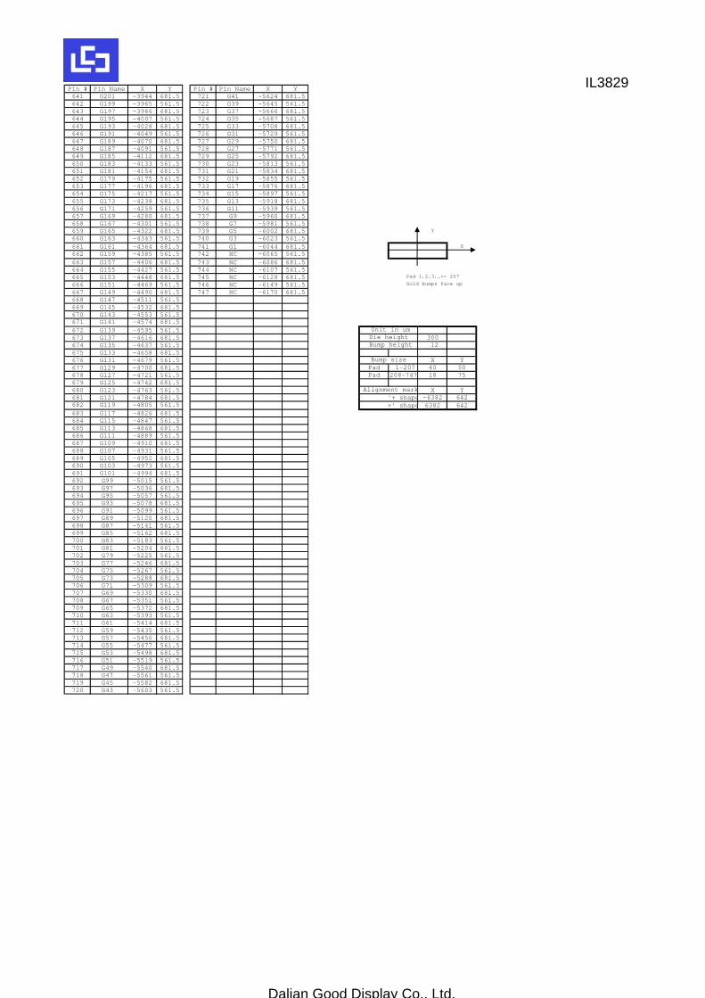
Pin # Pin Name X Y Pin # Pin Name X Y641 G201 -3944 681.5 721 G41 -5624 681.5642 G199 -3965 561.5 722 G39 -5645 561.5643 G197 -3986 681.5 723 G37 -5666 681.5644 G195 -4007 561.5 724 G35 -5687 561.5645 G193 -4028 681.5 725 G33 -5708 681.5646 G191 -4049 561.5 726 G31 -5729 561.5647 G189 -4070 681.5 727 G29 -5750 681.5648 G187 -4091 561.5 728 G27 -5771 561.5649 G185 -4112 681.5 729 G25 -5792 681.5650 G183 -4133 561.5 730 G23 -5813 561.5651 G181 -4154 681.5 731 G21 -5834 681.5652 G179 -4175 561.5 732 G19 -5855 561.5653 G177 -4196 681.5 733 G17 -5876 681.5654 G175 -4217 561.5 734 G15 -5897 561.5655 G173 -4238 681.5 735 G13 -5918 681.5656 G171 -4259 561.5 736 G11 -5939 561.5657 G169 -4280 681.5 737 G9 -5960 681.5658 G167 -4301 561.5 738 G7 -5981 561.5659 G165 -4322 681.5 739 G5 -6002 681.5 Y
660 G163 -4343 561.5 740 G3 -6023 561.5661 G161 -4364 681.5 741 G1 -6044 681.5 X
662 G159 -4385 561.5 742 NC -6065 561.5663 G157 -4406 681.5 743 NC -6086 681.5664 G155 -4427 561.5 744 NC -6107 561.5665 G153 -4448 681.5 745 NC -6128 681.5666 G151 -4469 561.5 746 NC -6149 561.5667 G149 -4490 681.5 747 NC -6170 681.5668 G147 -4511 561.5669 G145 -4532 681.5670 G143 -4553 561.5671 G141 -4574 681.5672 G139 -4595 561.5673 G137 -4616 681.5 300674 G135 -4637 561.5 12675 G133 -4658 681.5676 G131 -4679 561.5 X Y677 G129 -4700 681.5 Pad 1-207 40 50678 G127 -4721 561.5 Pad 208-747 18 75679 G125 -4742 681.5680 G123 -4763 561.5 X Y681 G121 -4784 681.5 '+ shape -6382 642682 G119 -4805 561.5 +' shape 6382 642683 G117 -4826 681.5684 G115 -4847 561.5685 G113 -4868 681.5686 G111 -4889 561.5687 G109 -4910 681.5688 G107 -4931 561.5689 G105 -4952 681.5690 G103 -4973 561.5691 G101 -4994 681.5692 G99 -5015 561.5693 G97 -5036 681.5694 G95 -5057 561.5695 G93 -5078 681.5696 G91 -5099 561.5697 G89 -5120 681.5698 G87 -5141 561.5699 G85 -5162 681.5700 G83 -5183 561.5701 G81 -5204 681.5702 G79 -5225 561.5703 G77 -5246 681.5704 G75 -5267 561.5705 G73 -5288 681.5706 G71 -5309 561.5707 G69 -5330 681.5708 G67 -5351 561.5709 G65 -5372 681.5710 G63 -5393 561.5711 G61 -5414 681.5712 G59 -5435 561.5713 G57 -5456 681.5714 G55 -5477 561.5715 G53 -5498 681.5716 G51 -5519 561.5717 G49 -5540 681.5718 G47 -5561 561.5719 G45 -5582 681.5720 G43 -5603 561.5
Bump height
Bump size
Alignment mark
Pad 1,2,3,…>> 207 Gold Bumps face up
Unit in umDie height
IL3829
Dalian Good Display Co., Ltd.
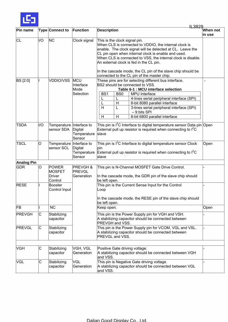
6 PIN DESCRIPTION Key: I = Input, O =Output, IO = Bi-directional (input/output), P = Power pin, C = Capacitor Pin
NC = Not Connected, Pull L =connect to VSS, Pull H = connect to VDDIO
Pin name Type Connect to Function Description When not in use
Input power VCI P Power
Supply Power Supply Power Supply for the chip
-
VCIA P Power Supply
Power Supply Power input for the chip, Connected with VCI
-
VCIBG P Power Supply
Power Supply Power input for the chip (Reference), Connected with VCI
-
VDDIO P Power
Supply Power for interface logic pins
Power Supply for the Interface It should be connected with VCI
-
VDD P Capacitor Regulator output
Core logic power pin VDD can be regulated internally from VCI. - For the single chip application, a capacitor should be
connected between VDD and VSS under all circumstances. - For the cascade mode application, a capacitor should be
connected between VDD and VSS in the master chip underall circumstances. For the slave chip, the capacitor is not necessary as VDD will be supplied from the cascade master chip externally.
-
EXTVDD I VDDIO/VSS Regulator bypass
This pin is VDD regulator bypass pin. - For the single chip application, EXTVDD should be
connected to VSS. - For the cascade mode application, EXTVDD of the master
chip should be connected to VSS while EXTVDD of the slave chip should be connected to VDDIO.
-
VSS P VSS GND Ground (Digital) - VSSA P VSS GND Ground (Analog)
It should be connected with VSS. -
VSSBG P VSS GND Ground (Reference) Connected with VSS
-
VSSGS P VSS GND Ground (Output) Connected with VSS
-
VPP P Power
Supply OTP power Power Supply for OTP Programming
Open
Digital I/O D [7:0] I/O MPU Data Bus These pins are bi-directional data bus connecting to the MCU
data bus. SPI mode: D0: SCLK D1: SDIN
D[2] : OPEN D[7:3]: VDDIO or VSS
CS# I MPU Logic Control This pin is the chip select input connecting to the MCU. The chip is enabled for MCU communication only when CS# is pulled LOW in parallel interface.
VDDIO or VSS
IL3829
Dalian Good Display Co., Ltd.
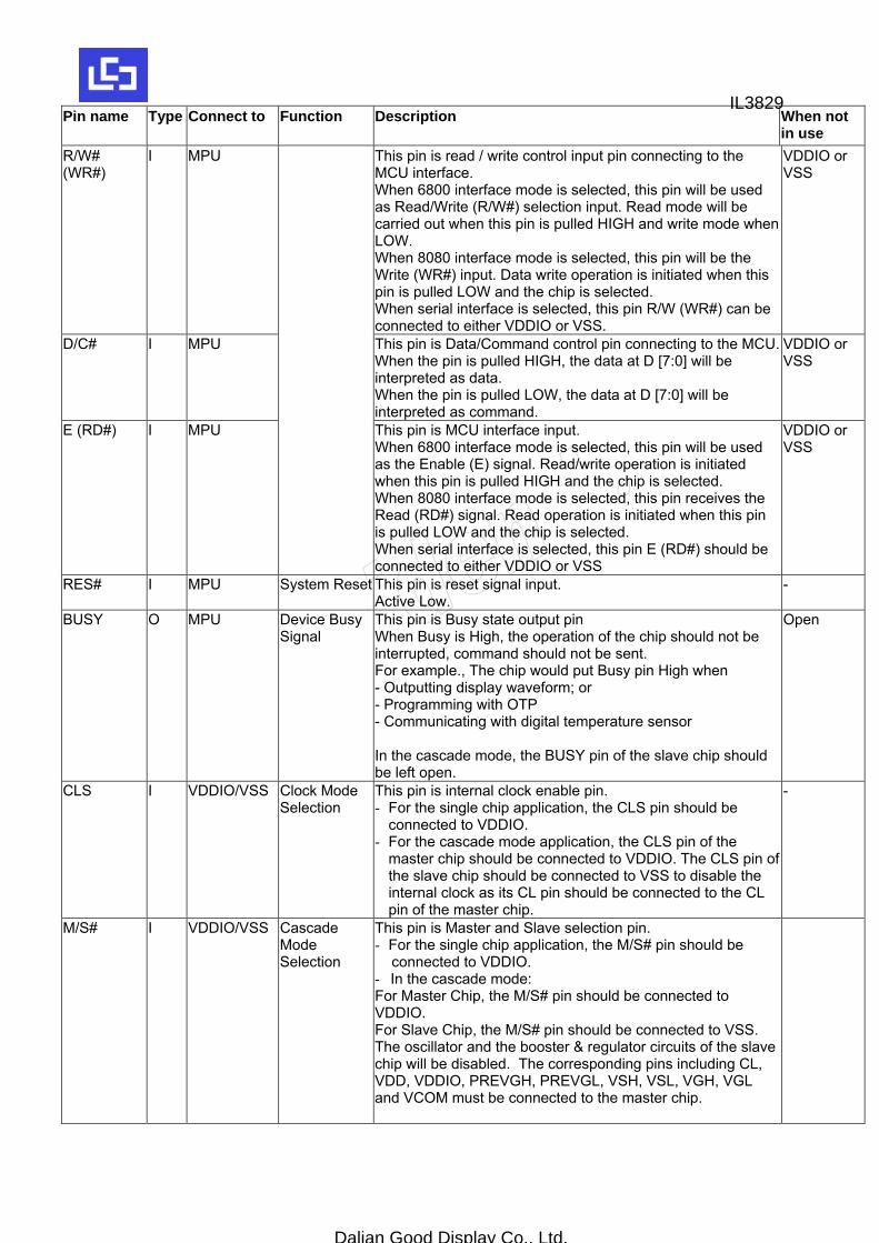
Pin name Type Connect to Function Description When not in use
R/W# (WR#)
I MPU This pin is read / write control input pin connecting to the MCU interface. When 6800 interface mode is selected, this pin will be used as Read/Write (R/W#) selection input. Read mode will be carried out when this pin is pulled HIGH and write mode when LOW. When 8080 interface mode is selected, this pin will be the Write (WR#) input. Data write operation is initiated when this pin is pulled LOW and the chip is selected. When serial interface is selected, this pin R/W (WR#) can be connected to either VDDIO or VSS.
VDDIO or VSS
D/C# I MPU This pin is Data/Command control pin connecting to the MCU. When the pin is pulled HIGH, the data at D [7:0] will be interpreted as data. When the pin is pulled LOW, the data at D [7:0] will be interpreted as command.
VDDIO or VSS
E (RD#) I MPU
This pin is MCU interface input. When 6800 interface mode is selected, this pin will be used as the Enable (E) signal. Read/write operation is initiated when this pin is pulled HIGH and the chip is selected. When 8080 interface mode is selected, this pin receives the Read (RD#) signal. Read operation is initiated when this pin is pulled LOW and the chip is selected. When serial interface is selected, this pin E (RD#) should be connected to either VDDIO or VSS
VDDIO or VSS
RES# I MPU System Reset This pin is reset signal input. Active Low.
-
BUSY O MPU Device Busy Signal
This pin is Busy state output pin When Busy is High, the operation of the chip should not be interrupted, command should not be sent. For example., The chip would put Busy pin High when - Outputting display waveform; or - Programming with OTP - Communicating with digital temperature sensor In the cascade mode, the BUSY pin of the slave chip should be left open.
Open
CLS I VDDIO/VSS Clock Mode Selection
This pin is internal clock enable pin. - For the single chip application, the CLS pin should be
connected to VDDIO. - For the cascade mode application, the CLS pin of the
master chip should be connected to VDDIO. The CLS pin of the slave chip should be connected to VSS to disable the internal clock as its CL pin should be connected to the CL pin of the master chip.
-
M/S# I VDDIO/VSS Cascade Mode Selection
This pin is Master and Slave selection pin. - For the single chip application, the M/S# pin should be
connected to VDDIO. - In the cascade mode: For Master Chip, the M/S# pin should be connected to VDDIO. For Slave Chip, the M/S# pin should be connected to VSS. The oscillator and the booster & regulator circuits of the slave chip will be disabled. The corresponding pins including CL, VDD, VDDIO, PREVGH, PREVGL, VSH, VSL, VGH, VGL and VCOM must be connected to the master chip.
IL3829
Dalian Good Display Co., Ltd.
Pin name Type Connect to Function Description When not in use
CL I/O NC Clock signal This is the clock signal pin. When CLS is connected to VDDIO, the internal clock is enable. The clock signal will be detected at CL. Leave the CL pin open when internal clock is enable and used. When CLS is connected to VSS, the internal clock is disable. An external clock is fed in the CL pin. In the cascade mode, the CL pin of the slave chip should be connected to the CL pin of the master chip.
BS [2:0] I VDDIO/VSS MCU Interface Mode Selection
These pins are for selecting different bus interface. BS2 should be connected to VSS.
Table 6-1 : MCU interface selection BS1 BS0 MPU Interface L L 4-lines serial peripheral interface (SPI) L H 8-bit 8080 parallel interface H L 3-lines serial peripheral interface (SPI)
– 9 bits SPI H H 8-bit 6800 parallel interface
-
TSDA I/O Temperature sensor SDA
Interface to Digital Temperature Sensor
This pin is I2C Interface to digital temperature sensor Data pinExternal pull up resistor is required when connecting to I2C slave
Open
TSCL O Temperature sensor SCL
Interface to Digital Temperature Sensor
This pin is I2C Interface to digital temperature sensor Clock pin External pull up resistor is required when connecting to I2C slave
Open
Analog Pin GDR O POWER
MOSFET Driver Control
This pin is N-Channel MOSFET Gate Drive Control. In the cascade mode, the GDR pin of the slave chip should be left open.
-
RESE I Booster Control Input
This pin is the Current Sense Input for the Control Loop In the cascade mode, the RESE pin of the slave chip should be left open.
-
FB I NC Keep open. Open
PREVGH C Stabilizing capacitor
This pin is the Power Supply pin for VGH and VSH. A stabilizing capacitor should be connected between PREVGH and VSS.
-
PREVGL C Stabilizing capacitor
PREVGH & PREVGL Generation
This pin is the Power Supply pin for VCOM, VGL and VSL. A stabilizing capacitor should be connected between PREVGL and VSS.
-
VGH C Stabilizing
capacitor VGH, VGL Generation
Positive Gate driving voltage. A stabilizing capacitor should be connected between VGH and VSS.
-
VGL C Stabilizing capacitor
VGL Generation
This pin is Negative Gate driving voltage. A stabilizing capacitor should be connected between VGL and VSS.
-
IL3829
Dalian Good Display Co., Ltd.
Pin name
Type Connect to Function Description When not in use
VSH C Stabilizing capacitor
This pin is Positive Source driving voltage. A stabilizing capacitor should be connected between VSH and VSS.
-
VSL C Stabilizing capacitor
VSH, VSL Generation
This pin is Negative Source driving voltage. A stabilizing capacitor should be connected between VSL and VSS.
-
VCOM C Panel/ Stabilizing capacitor
VCOM This pin is VCOM driving voltage A stabilizing capacitor should be connected between VCOM and VSS.
-
Panel Driving S [199:0]
O Panel Source driving signal
Source output pin
Open
G [299:0]
O Panel Gate driving signal
Gate output pin
Open
VBD O Panel Border driving signal
Border output pin
Open
Others NC NC NC Not Connected Keep open. Don’t connect with other NC pins Open
TPA NC NC Reserved for Testing
Keep open. Don’t connect to NC pin or other test pins including TPA, TPB, TPC, TPD and TPE.
Open
TPB NC NC Reserved for Testing
Keep open. Don’t connect to NC pin or other test pins including TPA, TPB, TPC, TPD and TPE.
Open
TPC NC NC Reserved for Testing
Keep open. Don’t connect to NC pin or other test pins including TPA, TPB, TPC, TPD and TPE.
Open
TPD NC NC Reserved for Testing
Keep open. Don’t connect to NC pin or other test pins including TPA, TPB, TPC, TPD and TPE.
Open
TIN I NC Reserved for Testing
Connect to TPE pin.
TPE O NC Reserved for Testing
Connect to TIN pin.
IL3829
Dalian Good Display Co., Ltd.
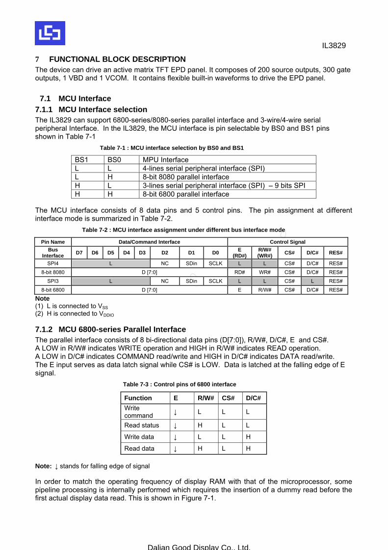
7 FUNCTIONAL BLOCK DESCRIPTION The device can drive an active matrix TFT EPD panel. It composes of 200 source outputs, 300 gate outputs, 1 VBD and 1 VCOM. It contains flexible built-in waveforms to drive the EPD panel.
7.1 MCU Interface 7.1.1 MCU Interface selection The IL3829 can support 6800-series/8080-series parallel interface and 3-wire/4-wire serial peripheral Interface. In the IL3829, the MCU interface is pin selectable by BS0 and BS1 pins shown in Table 7-1
Table 7-1 : MCU interface selection by BS0 and BS1
BS1 BS0 MPU Interface L L 4-lines serial peripheral interface (SPI) L H 8-bit 8080 parallel interface H L 3-lines serial peripheral interface (SPI) – 9 bits SPI H H 8-bit 6800 parallel interface
The MCU interface consists of 8 data pins and 5 control pins. The pin assignment at different interface mode is summarized in Table 7-2.
Table 7-2 : MCU interface assignment under different bus interface mode
Pin Name Data/Command Interface Control Signal Bus
Interface D7 D6 D5 D4 D3 D2 D1 D0 E (RD#)
R/W# (WR#) CS# D/C# RES#
SPI4 L NC SDin SCLK L L CS# D/C# RES#
8-bit 8080 D [7:0] RD# WR# CS# D/C# RES#
SPI3 L NC SDin SCLK L L CS# L RES#
8-bit 6800 D [7:0] E R/W# CS# D/C# RES#
Note (1) L is connected to VSS (2) H is connected to VDDIO 7.1.2 MCU 6800-series Parallel Interface The parallel interface consists of 8 bi-directional data pins (D[7:0]), R/W#, D/C#, E and CS#. A LOW in R/W# indicates WRITE operation and HIGH in R/W# indicates READ operation. A LOW in D/C# indicates COMMAND read/write and HIGH in D/C# indicates DATA read/write. The E input serves as data latch signal while CS# is LOW. Data is latched at the falling edge of E signal.
Table 7-3 : Control pins of 6800 interface
Function E R/W# CS# D/C#Write command ↓ L L L
Read status ↓ H L L
Write data ↓ L L H
Read data ↓ H L H Note: ↓ stands for falling edge of signal In order to match the operating frequency of display RAM with that of the microprocessor, some pipeline processing is internally performed which requires the insertion of a dummy read before the first actual display data read. This is shown in Figure 7-1.
IL3829
Dalian Good Display Co., Ltd.
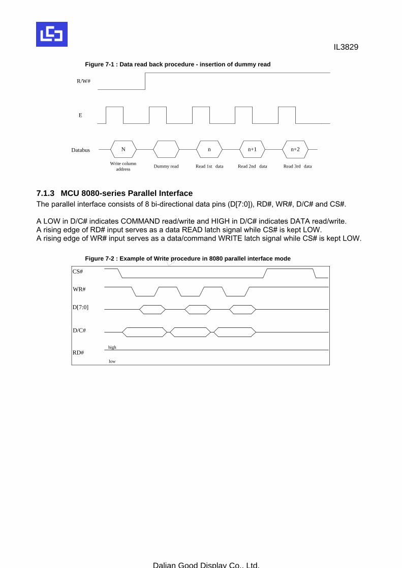
Figure 7-1 : Data read back procedure - insertion of dummy read
N n n+1 n+2
R/W#
E
Databus
Write columnaddress Read 1st dataDummy read Read 2nd data Read 3rd data
7.1.3 MCU 8080-series Parallel Interface The parallel interface consists of 8 bi-directional data pins (D[7:0]), RD#, WR#, D/C# and CS#. A LOW in D/C# indicates COMMAND read/write and HIGH in D/C# indicates DATA read/write. A rising edge of RD# input serves as a data READ latch signal while CS# is kept LOW. A rising edge of WR# input serves as a data/command WRITE latch signal while CS# is kept LOW.
Figure 7-2 : Example of Write procedure in 8080 parallel interface mode
CS#
WR#
D[7:0]
D/C#
RD#high
low
IL3829
Dalian Good Display Co., Ltd.
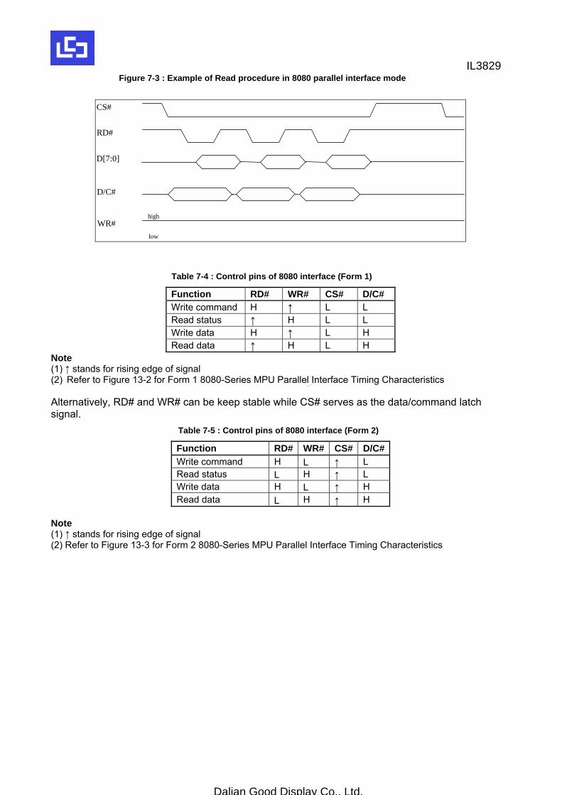
Figure 7-3 : Example of Read procedure in 8080 parallel interface mode
CS#
WR#
D[7:0]
D/C#
RD#
high
low
Table 7-4 : Control pins of 8080 interface (Form 1)
Function RD# WR# CS# D/C# Write command H ↑ L L Read status ↑ H L L Write data H ↑ L H Read data ↑ H L H
Note (1) ↑ stands for rising edge of signal (2) Refer to Figure 13-2 for Form 1 8080-Series MPU Parallel Interface Timing Characteristics Alternatively, RD# and WR# can be keep stable while CS# serves as the data/command latch signal.
Table 7-5 : Control pins of 8080 interface (Form 2)
Function RD# WR# CS# D/C#Write command H L ↑ L Read status L H ↑ L Write data H L ↑ H Read data L H ↑ H
Note (1) ↑ stands for rising edge of signal (2) Refer to Figure 13-3 for Form 2 8080-Series MPU Parallel Interface Timing Characteristics
IL3829
Dalian Good Display Co., Ltd.
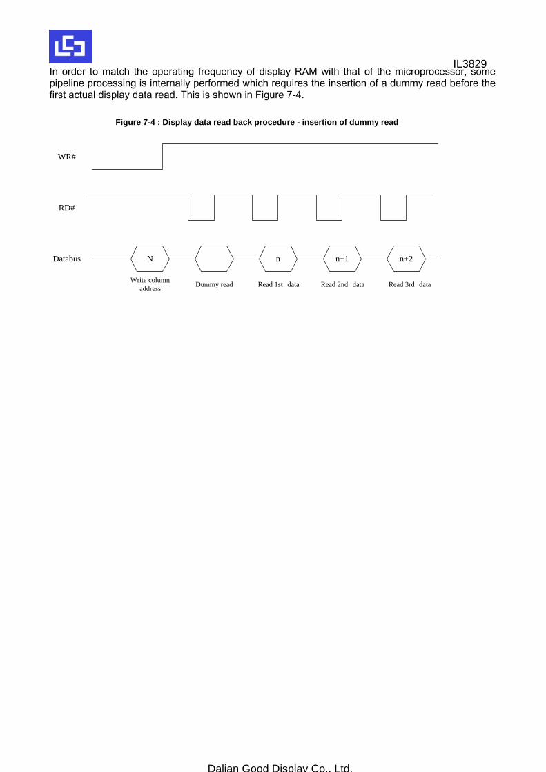
In order to match the operating frequency of display RAM with that of the microprocessor, some pipeline processing is internally performed which requires the insertion of a dummy read before the first actual display data read. This is shown in Figure 7-4.
Figure 7-4 : Display data read back procedure - insertion of dummy read
N n n+1 n+2
WR#
RD#
Databus
Write columnaddress Read 1st dataDummy read Read 2nd data Read 3rd data
IL3829
Dalian Good Display Co., Ltd.
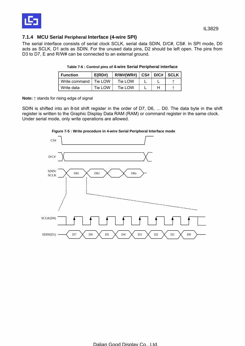
7.1.4 MCU Serial Peripheral Interface (4-wire SPI) The serial interface consists of serial clock SCLK, serial data SDIN, D/C#, CS#. In SPI mode, D0 acts as SCLK, D1 acts as SDIN. For the unused data pins, D2 should be left open. The pins from D3 to D7, E and R/W# can be connected to an external ground.
Table 7-6 : Control pins of 4-wire Serial Peripheral interface
Function E(RD#) R/W#(WR#) CS# D/C# SCLK Write command Tie LOW Tie LOW L L ↑ Write data Tie LOW Tie LOW L H ↑
Note: ↑ stands for rising edge of signal SDIN is shifted into an 8-bit shift register in the order of D7, D6, ... D0. The data byte in the shift register is written to the Graphic Display Data RAM (RAM) or command register in the same clock. Under serial mode, only write operations are allowed.
Figure 7-5 : Write procedure in 4-wire Serial Peripheral Interface mode
D7 D6 D5 D4 D3 D2 D1 D0
SCLK(D0)
SDIN(D1)
DB1 DB2 DBn
CS#
D/C#
SDIN/ SCLK
IL3829
Dalian Good Display Co., Ltd.
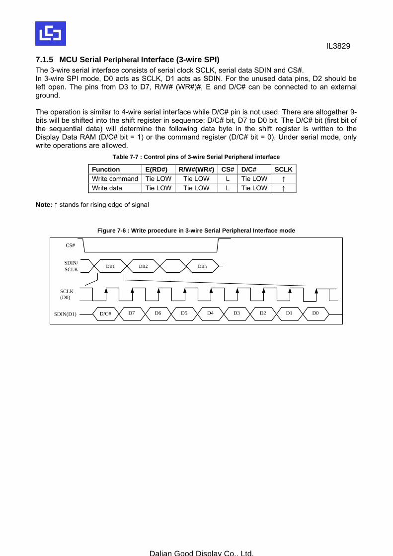
7.1.5 MCU Serial Peripheral Interface (3-wire SPI) The 3-wire serial interface consists of serial clock SCLK, serial data SDIN and CS#. In 3-wire SPI mode, D0 acts as SCLK, D1 acts as SDIN. For the unused data pins, D2 should be left open. The pins from D3 to D7, R/W# (WR#)#, E and D/C# can be connected to an external ground. The operation is similar to 4-wire serial interface while D/C# pin is not used. There are altogether 9-bits will be shifted into the shift register in sequence: D/C# bit, D7 to D0 bit. The D/C# bit (first bit of the sequential data) will determine the following data byte in the shift register is written to the Display Data RAM (D/C# bit = 1) or the command register (D/C# bit = 0). Under serial mode, only write operations are allowed.
Table 7-7 : Control pins of 3-wire Serial Peripheral interface
Function E(RD#) R/W#(WR#) CS# D/C# SCLK Write command Tie LOW Tie LOW L Tie LOW ↑ Write data Tie LOW Tie LOW L Tie LOW ↑
Note: ↑ stands for rising edge of signal
Figure 7-6 : Write procedure in 3-wire Serial Peripheral Interface mode
D7 D6 D5 D4 D3 D2 D1 D0
SCLK (D0)
SDIN(D1)
DB1 DB2 DBn
CS#
D/C#
SDIN/ SCLK
IL3829
Dalian Good Display Co., Ltd.
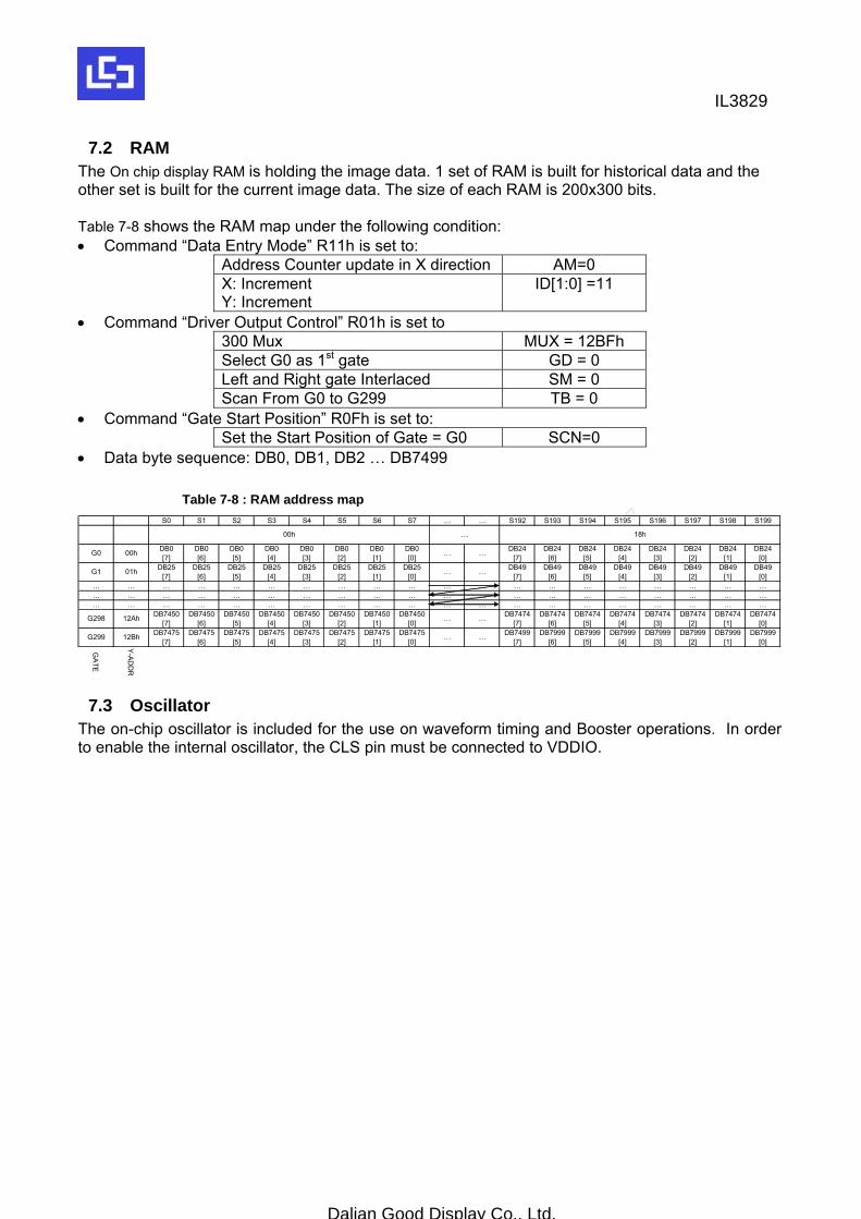
7.2 RAM The On chip display RAM is holding the image data. 1 set of RAM is built for historical data and the other set is built for the current image data. The size of each RAM is 200x300 bits. Table 7-8 shows the RAM map under the following condition: • Command “Data Entry Mode” R11h is set to:
Address Counter update in X direction AM=0 X: Increment Y: Increment
ID[1:0] =11
• Command “Driver Output Control” R01h is set to 300 Mux MUX = 12BFh Select G0 as 1st gate GD = 0 Left and Right gate Interlaced SM = 0 Scan From G0 to G299 TB = 0
• Command “Gate Start Position” R0Fh is set to: Set the Start Position of Gate = G0 SCN=0
• Data byte sequence: DB0, DB1, DB2 … DB7499
Table 7-8 : RAM address map S0 S1 S2 S3 S4 S5 S6 S7 … … S192 S193 S194 S195 S196 S197 S198 S199
DB0 DB0 DB0 DB0 DB0 DB0 DB0 DB0 DB24 DB24 DB24 DB24 DB24 DB24 DB24 DB24[7] [6] [5] [4] [3] [2] [1] [0] [7] [6] [5] [4] [3] [2] [1] [0]
DB25 DB25 DB25 DB25 DB25 DB25 DB25 DB25 DB49 DB49 DB49 DB49 DB49 DB49 DB49 DB49[7] [6] [5] [4] [3] [2] [1] [0] [7] [6] [5] [4] [3] [2] [1] [0]
… … … … … … … … … … … … … … … … … … … …… … … … … … … … … … … … … … … … … … … …… … … … … … … … … … … … … … … … … … … …
DB7450 DB7450 DB7450 DB7450 DB7450 DB7450 DB7450 DB7450 DB7474 DB7474 DB7474 DB7474 DB7474 DB7474 DB7474 DB7474[7] [6] [5] [4] [3] [2] [1] [0] [7] [6] [5] [4] [3] [2] [1] [0]
DB7475 DB7475 DB7475 DB7475 DB7475 DB7475 DB7475 DB7475 DB7499 DB7999 DB7999 DB7999 DB7999 DB7999 DB7999 DB7999[7] [6] [5] [4] [3] [2] [1] [0] [7] [6] [5] [4] [3] [2] [1] [0]
GATE
Y-ADD
R
G299 12Bh … …
G298 12Ah … …
G1 01h … …
18h
G0 00h … …
00h …
7.3 Oscillator The on-chip oscillator is included for the use on waveform timing and Booster operations. In order to enable the internal oscillator, the CLS pin must be connected to VDDIO.
IL3829
Dalian Good Display Co., Ltd.
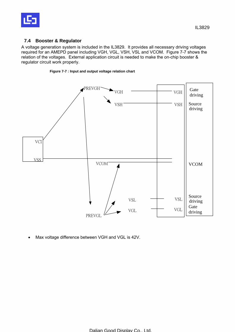
7.4 Booster & Regulator A voltage generation system is included in the IL3829. It provides all necessary driving voltages required for an AMEPD panel including VGH, VGL, VSH, VSL and VCOM. Figure 7-7 shows the relation of the voltages. External application circuit is needed to make the on-chip booster & regulator circuit work properly.
Figure 7-7 : Input and output voltage relation chart
VCI
VSSVCOM
PREVGL
VGH
VSH
VSL
VGL
VSH
VSL
VGL
VGHGatedriving
Sourcedriving
VCOM
PREVGH
Gatedriving
Sourcedriving
• Max voltage difference between VGH and VGL is 42V.
IL3829
Dalian Good Display Co., Ltd.
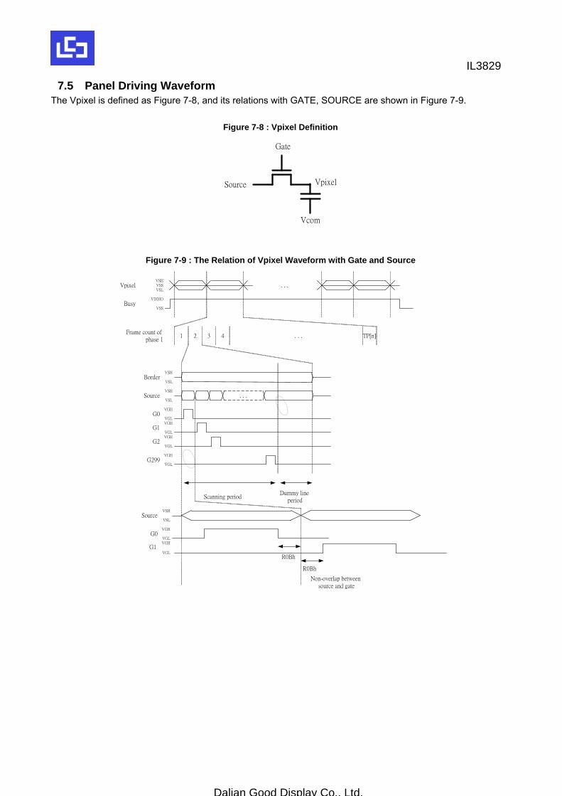
7.5 Panel Driving Waveform The Vpixel is defined as Figure 7-8, and its relations with GATE, SOURCE are shown in Figure 7-9.
Figure 7-8 : Vpixel Definition
Source
Gate
Vcom
Vpixel
Figure 7-9 : The Relation of Vpixel Waveform with Gate and Source
. . .
Border
Source
G0
G1
G2
G299
VGH
VGLVGH
VGLVGH
VGL
VGH
VGL
VSH
VSL
VSH
VSL
Scanning periodDummy line
period
Vpixel
Busy
VSH
VSLVSS
VDDIO
VSS
1 2 3 4 TP[n]Frame count of
phase 1. . .
. . .
Source
G0VGH
VGLVGH
VSH
VSL
G1VGL
R0Bh
Non-overlap between source and gate
R0Bh
IL3829
Dalian Good Display Co., Ltd.
7.6 VCOM Sensing This functional block provides the scheme to select the optimal VCOM DC level and programmed the setting into OTP.
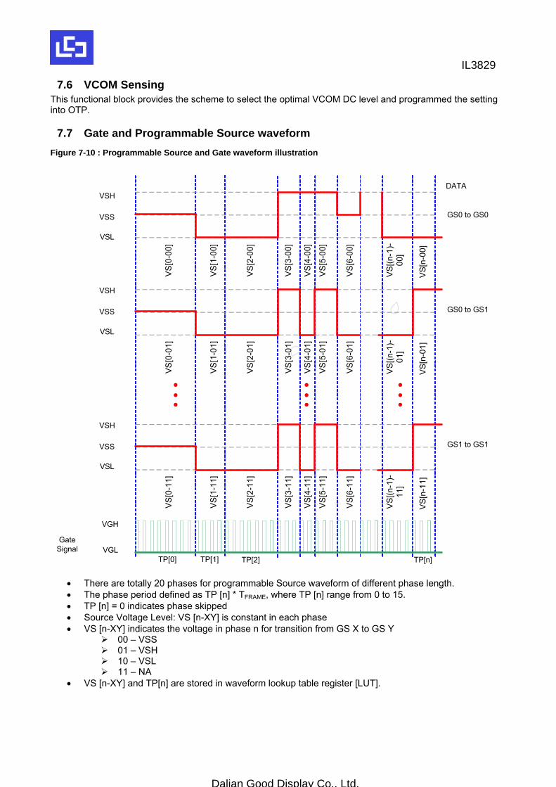
7.7 Gate and Programmable Source waveform Figure 7-10 : Programmable Source and Gate waveform illustration
VSH
VSS
VSL
DATA
GateSignal
GS0 to GS0
VSH
VSS
VSL
GS0 to GS1
VSH
VSS
VSL
GS1 to GS1
… … …
VGH
VGLTP[0] TP[1] TP[2] TP[n]
VS[
0-00
]
VS[
1-00
]
VS[
2-00
]
VS[
3-00
]
VS[
4-00
]
VS[
6-00
]
VS[
5-00
]
VS[(n
-1)-
00]
VS[
n-00
]
VS[0
-01]
VS[1
-01]
VS[2
-01]
VS[3
-01]
VS[4
-01]
VS[6
-01]
VS[5
-01]
VS[
(n-1
)-01
]
VS
[n-0
1]
VS[0
-11]
VS[1
-11]
VS[2
-11]
VS[3
-11]
VS[4
-11]
VS[6
-11]
VS[5
-11]
VS[
(n-1
)-11
]
VS[
n-11
]
• There are totally 20 phases for programmable Source waveform of different phase length. • The phase period defined as TP [n] * TFRAME, where TP [n] range from 0 to 15. • TP [n] = 0 indicates phase skipped • Source Voltage Level: VS [n-XY] is constant in each phase • VS [n-XY] indicates the voltage in phase n for transition from GS X to GS Y
00 – VSS 01 – VSH 10 – VSL 11 – NA
• VS [n-XY] and TP[n] are stored in waveform lookup table register [LUT].
IL3829
Dalian Good Display Co., Ltd.
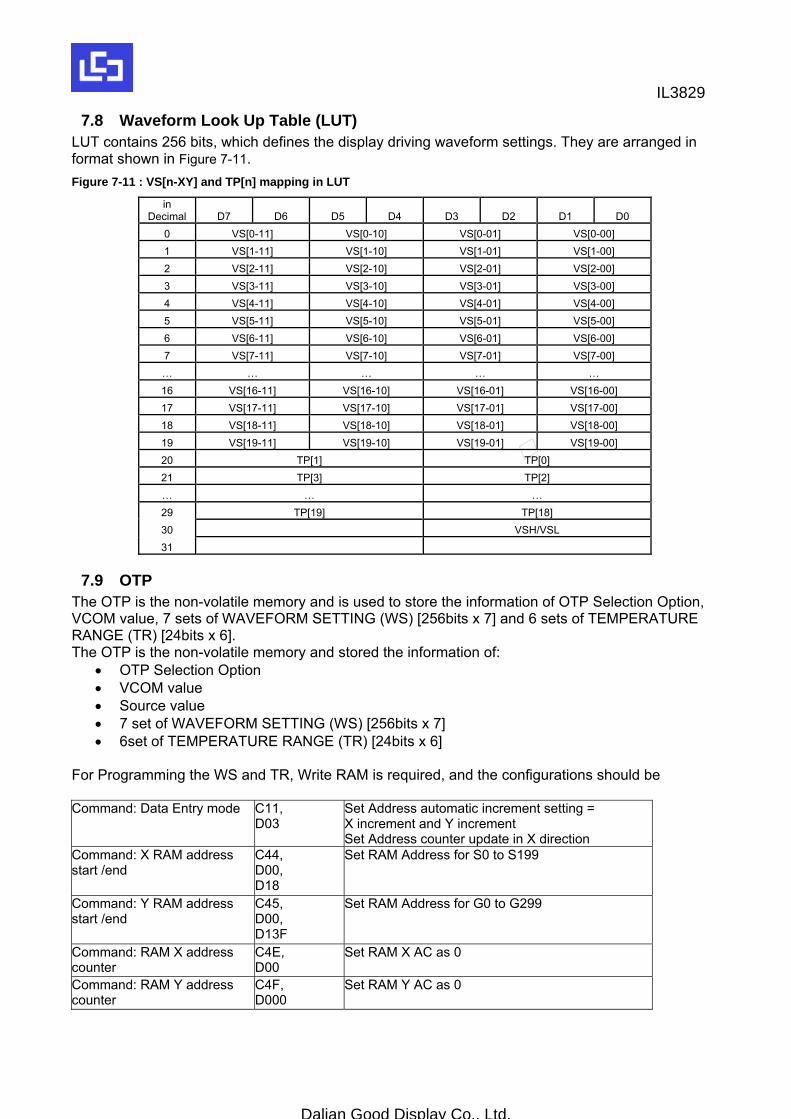
7.8 Waveform Look Up Table (LUT) LUT contains 256 bits, which defines the display driving waveform settings. They are arranged in format shown in Figure 7-11. Figure 7-11 : VS[n-XY] and TP[n] mapping in LUT
in Decimal D7 D6 D5 D4 D3 D2 D1 D0
0 VS[0-11] VS[0-10] VS[0-01] VS[0-00] 1 VS[1-11] VS[1-10] VS[1-01] VS[1-00] 2 VS[2-11] VS[2-10] VS[2-01] VS[2-00] 3 VS[3-11] VS[3-10] VS[3-01] VS[3-00] 4 VS[4-11] VS[4-10] VS[4-01] VS[4-00] 5 VS[5-11] VS[5-10] VS[5-01] VS[5-00] 6 VS[6-11] VS[6-10] VS[6-01] VS[6-00] 7 VS[7-11] VS[7-10] VS[7-01] VS[7-00] … … … … … 16 VS[16-11] VS[16-10] VS[16-01] VS[16-00] 17 VS[17-11] VS[17-10] VS[17-01] VS[17-00] 18 VS[18-11] VS[18-10] VS[18-01] VS[18-00] 19 VS[19-11] VS[19-10] VS[19-01] VS[19-00] 20 TP[1] TP[0] 21 TP[3] TP[2] … … … 29 TP[19] TP[18] 30 VSH/VSL 31
7.9 OTP The OTP is the non-volatile memory and is used to store the information of OTP Selection Option, VCOM value, 7 sets of WAVEFORM SETTING (WS) [256bits x 7] and 6 sets of TEMPERATURE RANGE (TR) [24bits x 6]. The OTP is the non-volatile memory and stored the information of:
• OTP Selection Option • VCOM value • Source value • 7 set of WAVEFORM SETTING (WS) [256bits x 7] • 6set of TEMPERATURE RANGE (TR) [24bits x 6]
For Programming the WS and TR, Write RAM is required, and the configurations should be Command: Data Entry mode C11,
D03 Set Address automatic increment setting = X increment and Y increment Set Address counter update in X direction
Command: X RAM address start /end
C44, D00, D18
Set RAM Address for S0 to S199
Command: Y RAM address start /end
C45, D00, D13F
Set RAM Address for G0 to G299
Command: RAM X address counter
C4E, D00
Set RAM X AC as 0
Command: RAM Y address counter
C4F, D000
Set RAM Y AC as 0
IL3829
Dalian Good Display Co., Ltd.
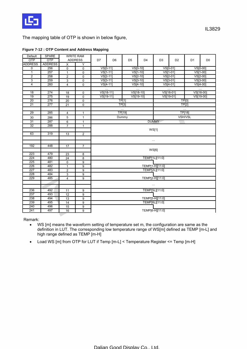
The mapping table of OTP is shown in below figure, Figure 7-12 : OTP Content and Address Mapping
Default SPAREOTP OTP
ADDRESS ADDRESS X Y0 256 0 01 257 1 02 258 2 03 259 3 04 260 4 0
18 274 18 019 275 19 020 276 20 021 277 21 0
29 285 4 130 286 5 131 287 6 132 288 7 1
63 319 13 2
192 448 17 7
223 479 23 8224 480 24 8225 481 0 9226 482 1 9227 483 2 9228 484 3 9229 485 4 9
236 492 11 9237 493 12 9238 494 13 9239 495 14 9240 496 15 9241 497 16 9
Dummy VSH/VSLDUMMY
TEMP[2L][11:0]
WRITE RAMADDRESS D7 D6
VS[19-11] VS[19-10]
TP[3]
TEMP[1-H][11:0]
D5 D0
… …VS[18-11] VS[18-10] VS[18-01] VS[18-00]
D4 D3 D2 D1
VS[4-10] VS[4-01] VS[4-00]… …
VS[0-11] VS[0-10] VS[0-01] VS[0-00]
VS[3-10] VS[3-01] VS[3-00]VS[4-11]
VS[1-11] VS[1-10] VS[1-01] VS[1-00]VS[2-11] VS[2-10] VS[2-01] VS[2-00]VS[3-11]
VS[19-01] VS[19-00]TP[1] TP[0]
TP[2]… …
TP[19] TP[18]
TEMP[5-H][11:0]
WS[1]
…
WS[6]
TEMP[1L][11:0]
TEMP[2-H][11:0]
…
TEMP[6L][11:0]
TEMP[6-H][11:0]
TEMP[5L][11:0]
Remark:
• WS [m] means the waveform setting of temperature set m, the configuration are same as the definition in LUT. The corresponding low temperature range of WS[m] defined as TEMP [m-L] and high range defined as TEMP [m-H]
• Load WS [m] from OTP for LUT if Temp [m-L] < Temperature Register <= Temp [m-H]
IL3829
Dalian Good Display Co., Ltd.
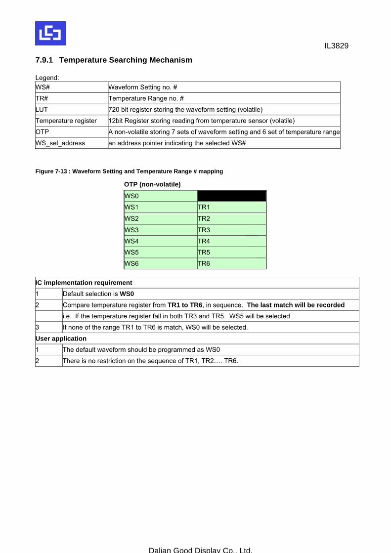
7.9.1 Temperature Searching Mechanism Legend: WS# Waveform Setting no. # TR# Temperature Range no. # LUT 720 bit register storing the waveform setting (volatile) Temperature register 12bit Register storing reading from temperature sensor (volatile) OTP A non-volatile storing 7 sets of waveform setting and 6 set of temperature range
WS_sel_address an address pointer indicating the selected WS# Figure 7-13 : Waveform Setting and Temperature Range # mapping
OTP (non-volatile) WS0 WS1 TR1 WS2 TR2 WS3 TR3 WS4 TR4 WS5 TR5 WS6 TR6
IC implementation requirement 1 Default selection is WS0 2 Compare temperature register from TR1 to TR6, in sequence. The last match will be recorded i.e. If the temperature register fall in both TR3 and TR5. WS5 will be selected 3 If none of the range TR1 to TR6 is match, WS0 will be selected. User application 1 The default waveform should be programmed as WS0 2 There is no restriction on the sequence of TR1, TR2…. TR6.
IL3829
Dalian Good Display Co., Ltd.
7.10 External Temperature Sensor I2C Single Master Interface The chip provides two I/O lines [TSDA and TSCL] for connecting digital temperature sensor for temperature reading sensing. TSDA will treat as SDA line and TSCL will treat as SCL line. They are required connecting with external pull-up resistor. 1. If the Temperature value MSByte bit D11 = 0, then The temperature is positive and value (DegC) = + (Temperature value) / 16 2. If the Temperature value MSByte bit D11 = 1, then The temperature is negative and value (DegC) = ~ (2’s complement of Temperature value) / 16
12-bit binary (2's complement)
Hexadecimal Value
Decimal Value
Value [DegC]
0111 1111 0000 7F0 2032 127 0111 1110 1110 7EE 2030 126.875 0111 1110 0010 7E2 2018 126.125 0111 1101 0000 7D0 2000 125 0001 1001 0000 190 400 25 0000 0000 0010 002 2 0.125 0000 0000 0000 000 0 0 1111 1111 1110 FFE -2 -0.125 1110 0111 0000 E70 -400 -25 1100 1001 0010 C92 -878 -54.875 1100 1001 0000 C90 -880 -55
7.11 Cascade Mode The IL3829 has a cascade mode that can cascade 2 chips to achieve the display resolution up to 400 (sources) x 300 (gates). The pin M/S# is used to configure the chip. When M/S# is connected to VDDIO, the chip is configured as a master chip. When M/S# is connected to VSS, the chip is configured as a slave chip. When the chip is configured as a master chip, it will be the same as a single chip application, ie, all circuit blocks will be worked as usual. When the chip is configured as a slave chip, its oscillator and booster & regulator circuit will be disabled. The oscillator clock and all booster voltages will be come from the master chip. Therefore, the corresponding pins including CL, VDD, PREVGH, PREVGL, VSH, VSL, VGH, VGL and VCOM must be connected to the master chip.
IL3829
Dalian Good Display Co., Ltd.
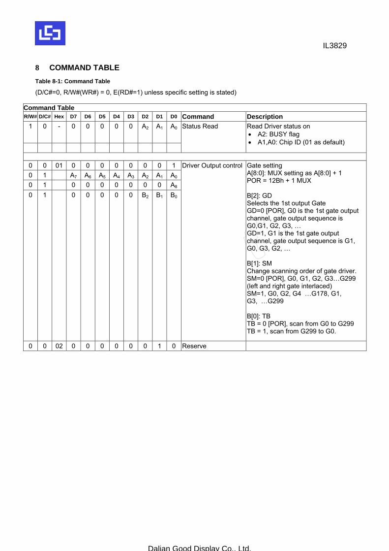
8 COMMAND TABLE Table 8-1: Command Table
(D/C#=0, R/W#(WR#) = 0, E(RD#=1) unless specific setting is stated)
Command Table R/W# D/C# Hex D7 D6 D5 D4 D3 D2 D1 D0 Command Description
1 0 - 0 0 0 0 0 A2 A1 A0
Status Read Read Driver status on • A2: BUSY flag • A1,A0: Chip ID (01 as default)
0 0 01 0 0 0 0 0 0 0 10 1 A7 A6 A5 A4 A3 A2 A1 A0
0 1 0 0 0 0 0 0 0 A8
0 1 0 0 0 0 0 B2 B1 B0
Driver Output control Gate setting A[8:0]: MUX setting as A[8:0] + 1 POR = 12Bh + 1 MUX B[2]: GD Selects the 1st output Gate GD=0 [POR], G0 is the 1st gate output channel, gate output sequence is G0,G1, G2, G3, … GD=1, G1 is the 1st gate output channel, gate output sequence is G1, G0, G3, G2, … B[1]: SM Change scanning order of gate driver. SM=0 [POR], G0, G1, G2, G3…G299 (left and right gate interlaced) SM=1, G0, G2, G4 …G178, G1, G3, …G299 B[0]: TB TB = 0 [POR], scan from G0 to G299 TB = 1, scan from G299 to G0.
0 0 02 0 0 0 0 0 0 1 0 Reserve
IL3829
Dalian Good Display Co., Ltd.
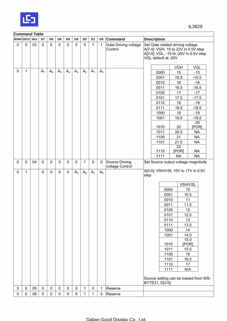
Command Table R/W# D/C# Hex D7 D6 D5 D4 D3 D2 D1 D0 Command Description
0 0 03 0 0 0 0 0 0 1 1 Gate Driving voltage Control
0 1 A7 A6 A5 A4 A3 A2 A1 A0
Set Gate related driving voltage A[7:4]: VGH, 15 to 22V in 0.5V step A[3:0]: VGL, -15 to -20V in 0.5V step VGL default at -20V
VGH VGL 0000 15 -15 0001 15.5 -15.5 0010 16 -16 0011 16.5 -16.5 0100 17 -17 0101 17.5 -17.5 0110 18 -18 0111 18.5 -18.5 1000 19 -19 1001 19.5 -19.5
1010 20 -20
[POR] 1011 20.5 NA 1100 21 NA 1101 21.5 NA
1110 22
[POR] NA 1111 NA NA
0 0 04 0 0 0 0 0 1 0 0 Source Driving voltage Control
0 1 0 0 0 0 A3 A2 A1 A0
Set Source output voltage magnitude A[3:0]: VSH/VSL 10V to 17V in 0.5V step
VSH/VSL
0000 10 0001 10.5 0010 11 0011 11.5 0100 12 0101 12.5 0110 13 0111 13.5 1000 14 1001 14.5
1010 15.0
[POR] 1011 15.5 1100 16 1101 16.5 1110 17 1111 N/A
Source setting can be loaded from WS-BYTE31, D[3:0]
0 0 05 0 0 0 0 0 1 0 1 Reserve 0 0 06 0 0 0 0 0 1 1 0 Reserve
IL3829
Dalian Good Display Co., Ltd.
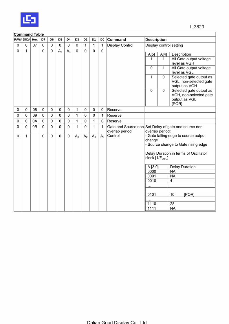
Command Table R/W# D/C# Hex D7 D6 D5 D4 D3 D2 D1 D0 Command Description
0 0 07 0 0 0 0 0 1 1 10 1 0 0 A5 A4 0 0 0 0
Display Control Display control setting
A[5] A[4] Description 1 1 All Gate output voltage
level as VGH 0 1 All Gate output voltage
level as VGL 1 0 Selected gate output as
VGL, non-selected gate output as VGH
0 0 Selected gate output as VGH, non-selected gate output as VGL [POR]
0 0 08 0 0 0 0 1 0 0 0 Reserve 0 0 09 0 0 0 0 1 0 0 1 Reserve 0 0 0A 0 0 0 0 1 0 1 0 Reserve 0 0 0B 0 0 0 0 1 0 1 1
0 1 0 0 0 0 A3 A2 A1 A0
Gate and Source non overlap period Control
Set Delay of gate and source non overlap period: - Gate falling edge to source output change - Source change to Gate rising edge Delay Duration in terms of Oscillator clock [1/FOSC]
A [3:0] Delay Duration 0000 NA 0001 NA 0010 4 … 0101 10 [POR] … 1110 28 1111 NA
IL3829
Dalian Good Display Co., Ltd.
Command Table R/W# D/C# Hex D7 D6 D5 D4 D3 D2 D1 D0 Command Description
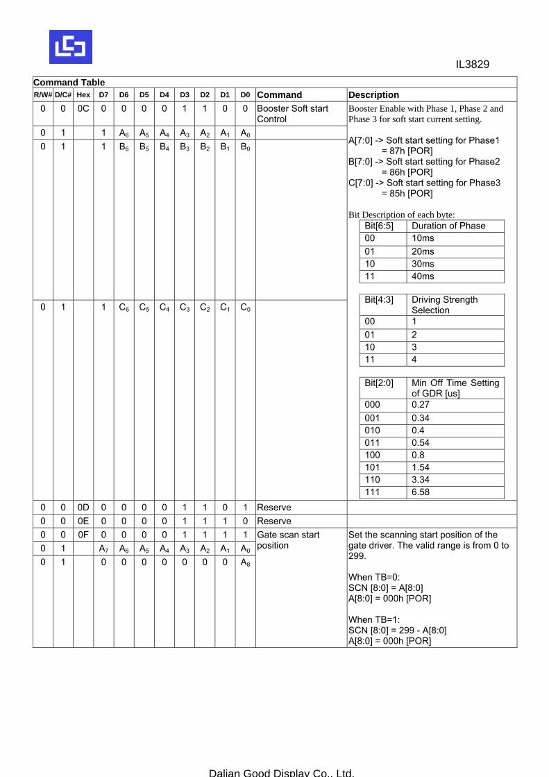
0 0 0C 0 0 0 0 1 1 0 0 Booster Soft start Control
0 1 1 A6 A5 A4 A3 A2 A1 A0 0 1 1 B6 B5 B4 B3 B2 B1 B0
0 1 1 C6 C5 C4 C3 C2 C1 C0
Booster Enable with Phase 1, Phase 2 and Phase 3 for soft start current setting. A[7:0] -> Soft start setting for Phase1 = 87h [POR] B[7:0] -> Soft start setting for Phase2 = 86h [POR] C[7:0] -> Soft start setting for Phase3 = 85h [POR] Bit Description of each byte:
Bit[6:5] Duration of Phase 00 10ms 01 20ms 10 30ms 11 40ms
Bit[4:3] Driving Strength
Selection 00 1 01 2 10 3 11 4
Bit[2:0] Min Off Time Setting
of GDR [us] 000 0.27 001 0.34 010 0.4 011 0.54 100 0.8 101 1.54 110 3.34 111 6.58
0 0 0D 0 0 0 0 1 1 0 1 Reserve 0 0 0E 0 0 0 0 1 1 1 0 Reserve 0 0 0F 0 0 0 0 1 1 1 10 1 A7 A6 A5 A4 A3 A2 A1 A0
0 1 0 0 0 0 0 0 0 A8
Gate scan start position
Set the scanning start position of the gate driver. The valid range is from 0 to 299. When TB=0: SCN [8:0] = A[8:0] A[8:0] = 000h [POR] When TB=1: SCN [8:0] = 299 - A[8:0] A[8:0] = 000h [POR]
IL3829
Dalian Good Display Co., Ltd.
Command Table R/W# D/C# Hex D7 D6 D5 D4 D3 D2 D1 D0 Command Description
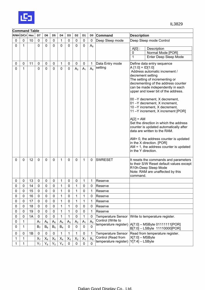
0 0 10 0 0 0 1 0 0 0 0 Deep Sleep mode 0 1 0 0 0 0 0 0 0 A0
Deep Sleep mode Control
A[0] : Description 0 Normal Mode [POR] 1 Enter Deep Sleep Mode
0 0 11 0 0 0 1 0 0 0 10 1 0 0 0 0 0 A2 A1 A0
Data Entry mode setting
Define data entry sequence A [1:0] = ID[1:0] Address automatic increment / decrement setting The setting of incrementing or decrementing of the address counter can be made independently in each upper and lower bit of the address. 00 –Y decrement, X decrement, 01 –Y decrement, X increment, 10 –Y increment, X decrement, 11 –Y increment, X increment [POR] A[2] = AM Set the direction in which the address counter is updated automatically after data are written to the RAM. AM= 0, the address counter is updated in the X direction. [POR] AM = 1, the address counter is updated in the Y direction.
0 0 12 0 0 0 1 0 0 1 0 SWRESET It resets the commands and parameters to their S/W Reset default values except R10h-Deep Sleep Mode Note: RAM are unaffected by this command.
0 0 13 0 0 0 1 0 0 1 1 Reserve 0 0 14 0 0 0 1 0 1 0 0 Reserve 0 0 15 0 0 0 1 0 1 0 1 Reserve 0 0 16 0 0 0 1 0 1 1 0 Reserve 0 0 17 0 0 0 1 0 1 1 1 Reserve 0 0 18 0 0 0 1 1 0 0 0 Reserve 0 0 19 0 0 0 1 1 0 0 1 Reserve 0 0 1A 0 0 0 1 1 0 1 00 1 A7 A6 A5 A4 A3 A2 A1 A0
0 1 B7 B6 B5 B4 0 0 0 0
Temperature Sensor Control (Write to temperature register)
Write to temperature register. A[7:0] – MSByte 01111111[POR] B[7:0] – LSByte 11110000[POR]
0 0 1B 0 0 0 1 1 1 0 11 1 X7 X6 X5 X4 X3 X2 X1 X0
1 1 Y7 Y6 Y5 Y4 0 0 0 0
Temperature Sensor Control (Read from temperature register)
Read from temperature register. X[7:0] – MSByte Y[7:4] – LSByte
IL3829
Dalian Good Display Co., Ltd.
Command Table R/W# D/C# Hex D7 D6 D5 D4 D3 D2 D1 D0 Command Description
0 0 1C 0 0 0 1 1 1 0 00 1 A7 A6 A5 A4 A3 A2 A1 A0
0 1 B7 B6 B5 B4 B3 B2 B1 B0
0 1 C7 C6 C5 C4 C3 C2 C1 C0
Temperature Sensor Control (Write Command to temperature sensor)
Write Command to temperature sensor A[7:6] – Select no of byte to be sent 00 – Address + pointer 01 – Address + pointer + 1st parameter 10 – Address + pointer + 1st parameter + 2nd pointer 11 – Address A[5:0] – Pointer Setting B[7:0] – 1st parameter C[7:0] – 2nd parameter The command required CLKEN=1.
0 0 1D 0 0 0 1 1 1 0 1 Temperature Sensor Control (Load temperature register with temperature sensor reading)
Load temperature register with temperature sensor reading BUSY=H for whole loading period The command required CLKEN=1.
0 0 1E 0 0 0 1 1 1 1 0 Reserve 0 0 1F 0 0 0 1 1 1 1 1 Reserve 0 0 20 0 0 1 0 0 0 0 0 Master Activation Activate Display Update Sequence
The Display Update Sequence Option is located at R22h User should not interrupt this operation to avoid corruption of panel images.
0 0 21 0 0 1 0 0 0 0 10 1 A7 0 0 A4 A3 A2 A1 A0
Display Update Control 1
Option for Display Update Bypass Option used for Pattern Display, which is used for display the RAM content into the Display OLD RAM Bypass option A [7] A[7] = 1: Enable bypass A[7] = 0: Disable bypass [POR] A[4] value will be used as for bypass. A[4] = 0 [POR] A[1:0] Initial Update Option - Source Control
A[1:0] GSC GSD 00 GS0 GS0
01 [POR] GS0 GS1 10 GS1 GS0 11 GS1 GS1
IL3829
Dalian Good Display Co., Ltd.
Command Table R/W# D/C# Hex D7 D6 D5 D4 D3 D2 D1 D0 Command Description
0 0 22 0 0 1 0 0 0 1 00 1 A7 A6 A5 A4 A3 A2 A1 A0
Display Update Control 2
Display Update Sequence Option: Enable the stage for Master Activation
Parameter (in Hex)
Enable Clock Signal, Then Enable CP Then Load Temperature value Then Load LUT Then INIITIAL DISPLAY Then PATTERN DISPLAY Then Disable CP Then Disable OSC
FF [POR]
Enable Clock Signal, Then Enable CP Then Load Temperature value Then Load LUT Then PATTERN DISPLAY Then Disable CP Then Disable OSC
F7
To Enable Clock Signal (CLKEN=1) 80
To Enable Clock Signal, then Enable CP (CLKEN=1, CPEN=1)
C0
To INITIAL DISPLAY + PATTEN DISPLAY 0C
To INITIAL DISPLAY 08 To DISPLAY PATTEN 04 To Disable CP, then Disable Clock Signal (CLKEN=1, CPEN=1)
03
To Disable Clock Signal (CLKEN=1) 01
Remark: CLKEN=1: If CLS=VDDIO then Enable OSC If CLS=VSS then Enable External Clock CLKEN=0: If CLS=VDDIO then Disable OSC AND INTERNAL CLOCK Signal = VSS,
0 0 23 0 0 1 0 0 0 1 1 Reserve
0 0 24 0 0 1 0 0 1 0 0 Write RAM
After this command, data entries will be written into the RAM until another command is written. Address pointers will advance accordingly.
0 0 25 0 0 1 0 0 1 0 1 Read RAM After this command, data read on the MCU bus will fetch data from RAM, until another command is written. Address pointers will advance accordingly.
0 0 26 0 0 1 0 0 1 1 0 Reserve 0 0 27 0 0 1 0 0 1 1 1 Reserve
IL3829
Dalian Good Display Co., Ltd.
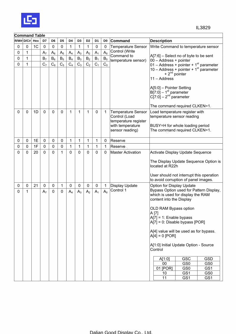
Command Table R/W# D/C# Hex D7 D6 D5 D4 D3 D2 D1 D0 Command Description
0 0 28 0 0 1 0 1 0 0 0 VCOM Sense Enter VCOM sensing conditions and hold for duration defined in 29h before reading VCOM value. The sensed VCOM voltage is stored in register The command required CLKEN=1.
0 0 29 0 0 1 0 1 0 0 10 1 0 0 0 0 A3 A2 A1 A0
VCOM Sense Duration Stabling time between entering VCOM sensing mode and reading acquired. VCOM sense duration = Setting + 1 Seconds 0x09(10Seconds) [POR]
0 0 2A 0 0 1 0 1 0 1 0 Program VCOM OTP Program VCOM register into OTP
0 0 2B 0 0 1 0 1 0 1 1 Reserve 0 0 2C 0 0 1 0 1 0 1 10 1 A7 A6 A5 A4 A3 A2 A1 A0
Write VCOM register Write VCOM register from MCU interface
0 0 2D 0 0 1 0 1 1 0 11 1 A7 A6 A5 A4 A3 A2 A1 A0
1 1 B7 B6 B5 B4 B3 B2 B1 B0
Read OTP Registers Read register reading to MCU A [7:0] Spare OTP Option B [7:0] VCOM Register
0 0 2E 0 0 1 0 1 1 1 0 Reserve 0 0 2F 0 0 1 0 1 1 1 1 Reserve 0 0 30 0 0 1 1 0 0 0 0 Program WS OTP Program OTP of Waveform Setting
The contents should be written into RAM before sending this command.
0 0 31 0 0 1 1 0 0 0 1 Reserve
0 0 32 0 0 1 1 0 0 1 0 Write LUT register
Write LUT register from MCU [240 bits], (excluding the VSH/VSL and Dummy bit)
0 0 0 … 0 0
1 1 1 … 1 1
LUT [30 bytes]
0 0 33 0 0 1 1 0 0 1 1 Read LUT register Read from LUT register [240 bits] (excluding the VSH/VSL and Dummy bit)
1 1 1 … 1 1
1 1 1 … 1 1
LUT [30 bytes]
IL3829
Dalian Good Display Co., Ltd.
Command Table R/W# D/C# Hex D7 D6 D5 D4 D3 D2 D1 D0 Command Description
0 0 34 0 0 1 1 0 1 0 0 Reserve 0 0 35 0 0 1 1 0 1 0 1 Reserve 0 0 36 0 0 1 1 0 1 1 0 Program OTP selection
Program OTP Selection according to the OTP Selection Control [R37h]
0 0 37 0 0 1 1 0 1 1 1 OTP selection Control
Write the OTP Selection:
A[7]=1 spare VCOM OTP A[6] VCOM_Status A[5]=1 spare WS OTP A[4] WS_Status
A[3:0] are reserved OTP bit. User can treat the bits as Version Control.
0 1 A7 A6 A5 A4 A3 A2 A1 A0 0 0 38 0 0 1 1 1 0 0 0 Reserve 0 0 39 0 0 1 1 1 0 0 1 Reserve
0 0 3A 0 0 1 1 1 0 1 00 1 0 A6 A5 A4 A3 A2 A1 A0
Set dummy line period
Set number of dummy line period A[6:0]: Number of dummy line period in term of TGate A[6:0] = 16h [POR] Available setting 0 to 127.
0 0 3B 0 0 1 1 1 0 1 10 1 0 0 0 0 A3 A2 A1 A0
Set Gate line width
Set Gate line width (TGate) A[3:0] Line width in us
A[3:0] TGate 0000 30 0001 34 0010 38 0011 40 0100 44 0101 46 0110 52 0111 56 1000 62 [POR] 1001 68 1010 78 1011 88 1100 104 1101 125 1110 156 1111 208
Remark: Default value will give 50Hz Frame frequency under 22 dummy line pulse setting.
IL3829
Dalian Good Display Co., Ltd.
Command Table R/W# D/C# Hex D7 D6 D5 D4 D3 D2 D1 D0 Command Description
0 0 3C 0 0 1 1 1 1 0 00 1 A7 A6 A5 A4 0 0 A1 A0
Border Waveform Control
Select border waveform for VBD A [7] Follow Source at Initial Update Display A [7]=0: [POR] A [7]=1: Follow Source at Initial Update Display for VBD, A [6:0] setting are being overridden at Initial Display STAGE. A [6] Select GS Transition/ Fix Level for VBD A [6]=0: Select GS Transition A[3:0] for VBD A [6]=1: Select FIX level Setting A[5:4] for VBD [POR] A [5:4] Fix Level Setting for VBD
A[5:4] VBD level00 VSS 01 VSH 10 VSL
11[POR] HiZ A [1:0] GS transition setting for VBD (Select waveform like data A[3:2] to data A[1:0])
A[1:0] GSA GSB00 GS0 GS0
01 [POR] GS0 GS1 10 GS1 GS0 11 GS1 GS1
0 0 3D 0 0 1 1 1 1 0 1 Reserve 0 0 3E 0 0 1 1 1 1 1 0 Reserve 0 0 3F 0 0 1 1 1 1 1 1 Reserve 0 0 40 0 1 0 0 0 0 0 0 Reserve 0 0 41 0 1 0 0 0 0 0 1 Reserve 0 0 42 0 1 0 0 0 0 1 0 Reserve 0 0 43 0 1 0 0 0 0 1 1 Reserve 0 0 44 0 1 0 0 0 1 0 00 1 0 0 0 A4 A3 A2 A1 A0
0 1 0 0 0 B4 B3 B2 B1 B0
Set RAM X - address Start / End position
Specify the start/end positions of the window address in the X direction by an address unit A[4:0]: XSA[4:0], XStart, POR = 00h B[4:0]: XEA[4:0], XEnd, POR = 18h
0 0 45 0 1 0 0 0 1 0 10 1 A7 A6 A5 A4 A3 A2 A1 A0
0 1 0 0 0 0 0 0 0 A8
0 1 B7 B6 B5 B4 B3 B2 B1 B0
0 1 0 0 0 0 0 0 0 B8
Set Ram Y- address Start / End position
Specify the start/end positions of the window address in the Y direction by an address unit A[8:0]: YSA[8:0], YStart, POR = 000h B[8:0]: YEA[8:0], YEnd, POR = 12Bh
0 0 46 0 1 0 0 0 1 1 0 Reserve 0 0 47 0 1 0 0 0 1 1 1 Reserve
IL3829
Dalian Good Display Co., Ltd.
Command Table R/W# D/C# Hex D7 D6 D5 D4 D3 D2 D1 D0 Command Description
0 0 48 0 1 0 0 1 0 0 0 Reserve 0 0 49 0 1 0 0 1 0 0 1 Reserve 0 0 4A 0 1 0 0 1 0 1 0 Reserve 0 0 4B 0 1 0 0 1 0 1 1 Reserve 0 0 4C 0 1 0 0 1 1 0 0 Reserve 0 0 4D 0 1 0 0 1 1 0 1 Reserve 0 0 4E 0 1 0 0 1 1 1 00 1 0 0 0 A4 A3 A2 A1 A0
Set RAM X address counter
Make initial settings for the RAM X address in the address counter (AC) A[4:0]: XAD[4:0], POR is 00h
0 0 4F 0 1 0 0 1 1 1 10 1 A7 A6 A5 A4 A3 A2 A1 A0
0 1 0 0 0 0 0 0 0 A8
Set RAM Y address counter
Make initial settings for the RAM Y address in the address counter (AC) A[8:0]: YAD8:0], POR is 000h
0 1 FF 1 1 1 1 1 1 1 1 NOP This command is an empty command; it does not have any effect on the display module. However it can be used to terminate Frame Memory Write or Read Commands.
IL3829
Dalian Good Display Co., Ltd.
9 Command DESCRIPTION
9.1 Driver Output Control (01h) This double byte command has multiple configurations and each bit setting is described as follows:
R/W DC IB7 IB6 IB5 IB4 IB3 IB2 IB1 IB0 W 1 MUX7 MUX6 MUX5 MUX4 MUX3 MUX2 MUX1 MUX0
POR 0 0 1 0 1 0 1 1 W 1 MUX8
POR 1 W 1 GD SM TB
POR 0 0 0 MUX[8:0]: Specify number of lines for the driver: MUX[8:0] + 1. Multiplex ratio (MUX ratio) from 16 MUX to 300MUX. GD: Selects the 1st output Gate
This bit is made to match the GATE layout connection on the panel. It defines the first scanning line. SM: Change scanning order of gate driver.
When SM is set to 0, left and right interlaced is performed. When SM is set to 1, no splitting odd / even of the GATE signal is performed, Output pin assignment sequence is shown as below (for 300 MUX ratio):
SM=0 SM=0 SM=1 SM=1
Driver GD=0 GD=1 GD=0 GD=1 G0 ROW0 ROW1 ROW0 ROW150 G1 ROW1 ROW0 ROW150 ROW0 G2 ROW2 ROW3 ROW1 ROW151 G3 ROW3 ROW2 ROW151 ROW1 : : : : :
G148 ROW148 ROW149 ROW74 ROW224 G149 ROW149 ROW148 ROW224 ROW74 G150 ROW150 ROW151 ROW75 ROW225 G151 ROW151 ROW150 ROW225 ROW75
: : : : : G296 ROW296 ROW297 ROW148 ROW298 G297 ROW297 ROW296 ROW298 ROW148 G298 ROW298 ROW299 ROW149 ROW299 G299 ROW299 ROW298 ROW299 ROW149
See “Scan Mode Setting” on next page.
TB: Change scanning direction of gate driver.
This bit defines the scanning direction of the gate for flexible layout of signals in module either from up to down (TB = 0) or from bottom to up (TB = 1).
IL3829
Dalian Good Display Co., Ltd.
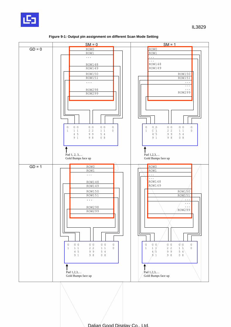
Figure 9-1: Output pin assignment on different Scan Mode Setting
SM = 0 SM = 1 GD = 0
GD = 1
Pad 1,2,3,… Gold Bumps face up
ROW150 ROW151 ... ROW298 ROW299
G G G G G G G G 1 1 1 2 2 1 1 0 4 5 9 9 5 4 9 1 9 8 0 8
ROW0 ROW1 ... ROW148 ROW149
Pad 1,2,3,… Gold Bumps face up
ROW0 ROW1 ... ... ROW148ROW149
G G G G G G G G 1 1 1 2 2 1 1 0 4 5 9 9 5 4 9 1 9 8 0 8
ROW150 ROW151
...
...
... ROW299
Pad 1, 2, 3,… Gold Bumps face up
ROW150 ROW151 ... ROW298 ROW299
G G G G G G G G 1 1 1 2 2 1 1 0 4 5 9 9 5 4 9 1 9 8 0 8
ROW0 ROW1 ... ROW148 ROW149
Pad 1,2,3,… Gold Bumps face up
ROW0 ROW1 ... ... ROW148ROW149
G G G G G G G G 1 1 1 2 2 1 1 0 4 5 9 9 5 4 9 1 9 8 0 8
ROW150 ROW151
...
...
... ROW299
IL3829
Dalian Good Display Co., Ltd.
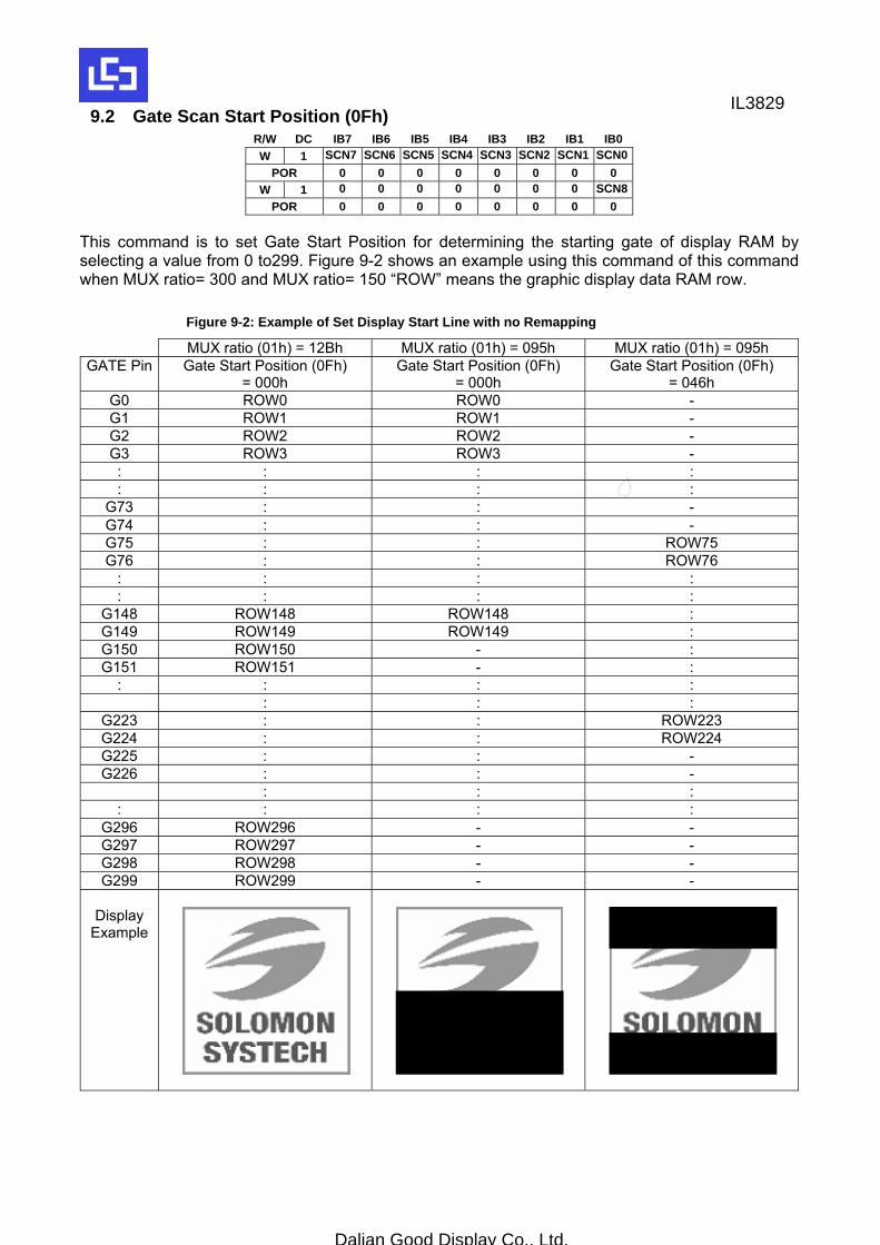
9.2 Gate Scan Start Position (0Fh) R/W DC IB7 IB6 IB5 IB4 IB3 IB2 IB1 IB0 W 1 SCN7 SCN6 SCN5 SCN4 SCN3 SCN2 SCN1 SCN0
POR 0 0 0 0 0 0 0 0 W 1 0 0 0 0 0 0 0 SCN8
POR 0 0 0 0 0 0 0 0 This command is to set Gate Start Position for determining the starting gate of display RAM by selecting a value from 0 to299. Figure 9-2 shows an example using this command of this command when MUX ratio= 300 and MUX ratio= 150 “ROW” means the graphic display data RAM row.
Figure 9-2: Example of Set Display Start Line with no Remapping
MUX ratio (01h) = 12Bh MUX ratio (01h) = 095h MUX ratio (01h) = 095h GATE Pin Gate Start Position (0Fh)
= 000h Gate Start Position (0Fh)
= 000h Gate Start Position (0Fh)
= 046h G0 ROW0 ROW0 - G1 ROW1 ROW1 - G2 ROW2 ROW2 - G3 ROW3 ROW3 - : : : : : : : :
G73 : : - G74 : : - G75 : : ROW75 G76 : : ROW76
: : : : : : : :
G148 ROW148 ROW148 : G149 ROW149 ROW149 : G150 ROW150 - : G151 ROW151 - :
: : : : : : :
G223 : : ROW223 G224 : : ROW224 G225 : : - G226 : : -
: : : : : : :
G296 ROW296 - - G297 ROW297 - - G298 ROW298 - - G299 ROW299 - -
Display
Example
IL3829
Dalian Good Display Co., Ltd.
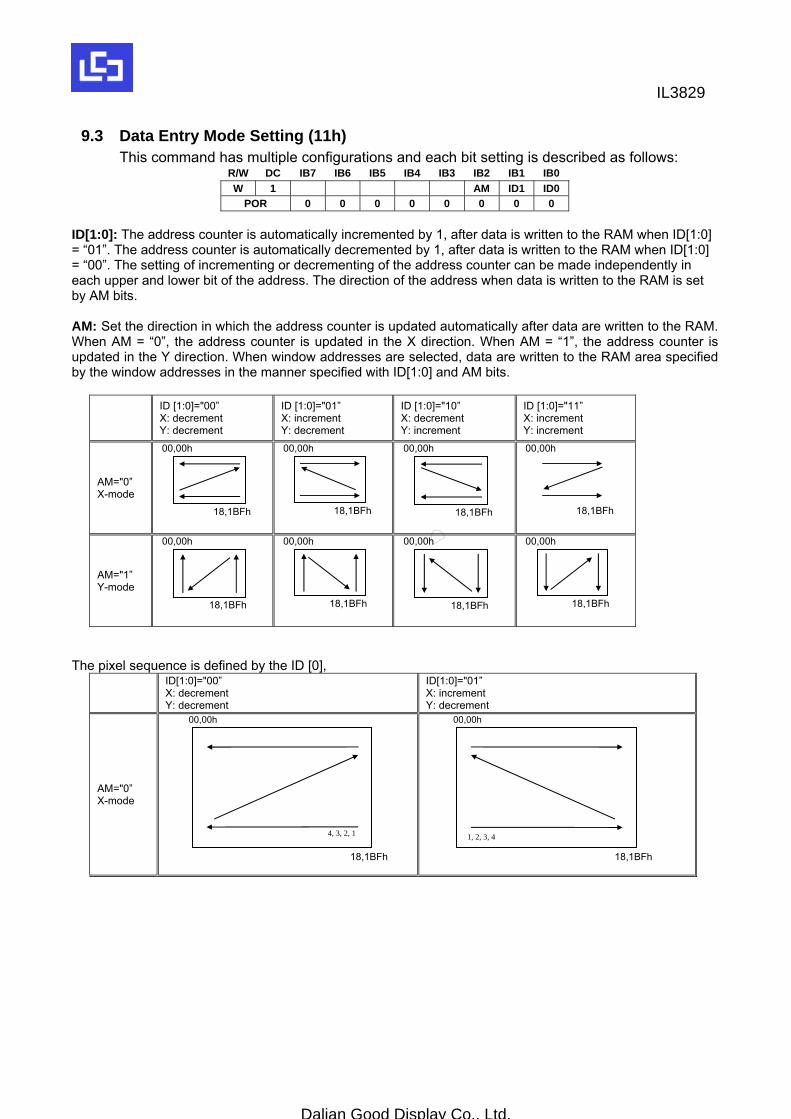
00,00h
18,1BFh
4, 3, 2, 1
9.3 Data Entry Mode Setting (11h) This command has multiple configurations and each bit setting is described as follows:
R/W DC IB7 IB6 IB5 IB4 IB3 IB2 IB1 IB0 W 1 AM ID1 ID0
POR 0 0 0 0 0 0 0 0 ID[1:0]: The address counter is automatically incremented by 1, after data is written to the RAM when ID[1:0] = “01”. The address counter is automatically decremented by 1, after data is written to the RAM when ID[1:0] = “00”. The setting of incrementing or decrementing of the address counter can be made independently in each upper and lower bit of the address. The direction of the address when data is written to the RAM is set by AM bits. AM: Set the direction in which the address counter is updated automatically after data are written to the RAM. When AM = “0”, the address counter is updated in the X direction. When AM = “1”, the address counter is updated in the Y direction. When window addresses are selected, data are written to the RAM area specified by the window addresses in the manner specified with ID[1:0] and AM bits.
ID [1:0]="00” X: decrement Y: decrement
ID [1:0]="01” X: increment Y: decrement
ID [1:0]="10” X: decrement Y: increment
ID [1:0]="11” X: increment Y: increment
AM="0” X-mode
AM="1” Y-mode
The pixel sequence is defined by the ID [0],
ID[1:0]="00” X: decrement Y: decrement
ID[1:0]="01” X: increment Y: decrement
AM="0” X-mode
00,00h
18,1BFh
00,00h
18,1BFh
00,00h
18,1BFh
00,00h
18,1BFh 00,00h
18,1BFh
00,00h
18,1BFh
00,00h
18,1BFh
00,00h
18,1BFh
00,00h
18,1BFh
1, 2, 3, 4
IL3829
Dalian Good Display Co., Ltd.
9.4 Set RAM X - Address Start / End Position (44h)
R/W DC IB7 IB6 IB5 IB4 IB3 IB2 IB1 IB0W 1 XSA4 XSA3 XSA2 XSA1 XSA0
POR 0 0 0 0 0 0 0 0 W 1 XEA4 XEA3 XEA2 XEA1 XEA0
POR 0 0 0 1 1 1 1 1 XSA[4:0]/XEA[4:0]: Specify the start/end positions of the window address in the X direction by 8 times address unit. Data is written to the RAM within the area determined by the addresses specified by XSA [4:0] and XEA [4:0]. These addresses must be set before the RAM write. It allows on XEA [4:0] ≤ XSA [4:0]. The settings follow the condition on 00h ≤ XSA [4:0], XEA [4:0] ≤ 18h. The windows is followed by the control setting of Data Entry Setting (R11h)
9.5 Set RAM Y - Address Start / End Position (45h) R/W DC IB7 IB6 IB5 IB4 IB3 IB2 IB1 IB0W 1 YSA7 YSA6 YSA5 YSA4 YSA3 YSA2 YSA1 YSA0
POR 0 0 0 0 0 0 0 0 W 1 0 0 0 0 0 0 0 YSA8
POR 0 0 0 0 0 0 0 0 W 1 YEA7 YEA6 YEA5 YEA4 YEA3 YEA2 YEA1 YEA0
POR 1 1 0 1 0 0 1 1 W 1 0 0 0 0 0 0 0 YEA8
POR 1 1 0 1 0 0 1 1 YSA[8:0]/YEA[8:0]: Specify the start/end positions of the window address in the Y direction by an address unit. Data is written to the RAM within the area determined by the addresses specified by YSA [8:0] and YEA [8:0]. These addresses must be set before the RAM write. It allows YEA [8:0] ≤ YSA [8:0]. The settings follow the condition on 00h ≤ YSA [8:0], YEA [8:0] ≤ 1BFh. The windows is followed by the control setting of Data Entry Setting (R11h)
9.6 Set RAM Address Counter (4Eh-4Fh) Reg# R/W DC IB7 IB6 IB5 IB4 IB3 IB2 IB1 IB0
W 1 XAD4 XAD3 XAD2 XAD1 XAD0 4Eh POR 0 0 0 0 0 0 0 0
W 1 YAD7 YAD6 YAD5 YAD4 YAD3 YAD2 YAD1 YAD0 4Fh POR 0 0 0 0 0 0 0 0
W 1 YAD8 4Fh POR 0
XAD[4:0]: Make initial settings for the RAM X address in the address counter (AC). YAD[8:0]: Make initial settings for the RAM Y address in the address counter (AC). After RAM data is written, the address counter is automatically updated according to the settings with AM, ID bits and setting for a new RAM address is not required in the address counter. Therefore, data is written consecutively without setting an address. The address counter is not automatically updated when data is read out from the RAM. RAM address setting cannot be made during the standby mode. The address setting should be made within the area designated with window addresses which is controlled by the Data Entry Setting (R11h) {AM, ID[1:0]} ; RAM Address XStart / XEnd Position (R44h) and RAM Address Ystart /Yend Position (R45h). Otherwise undesirable image will be displayed on the Panel.
IL3829
Dalian Good Display Co., Ltd.
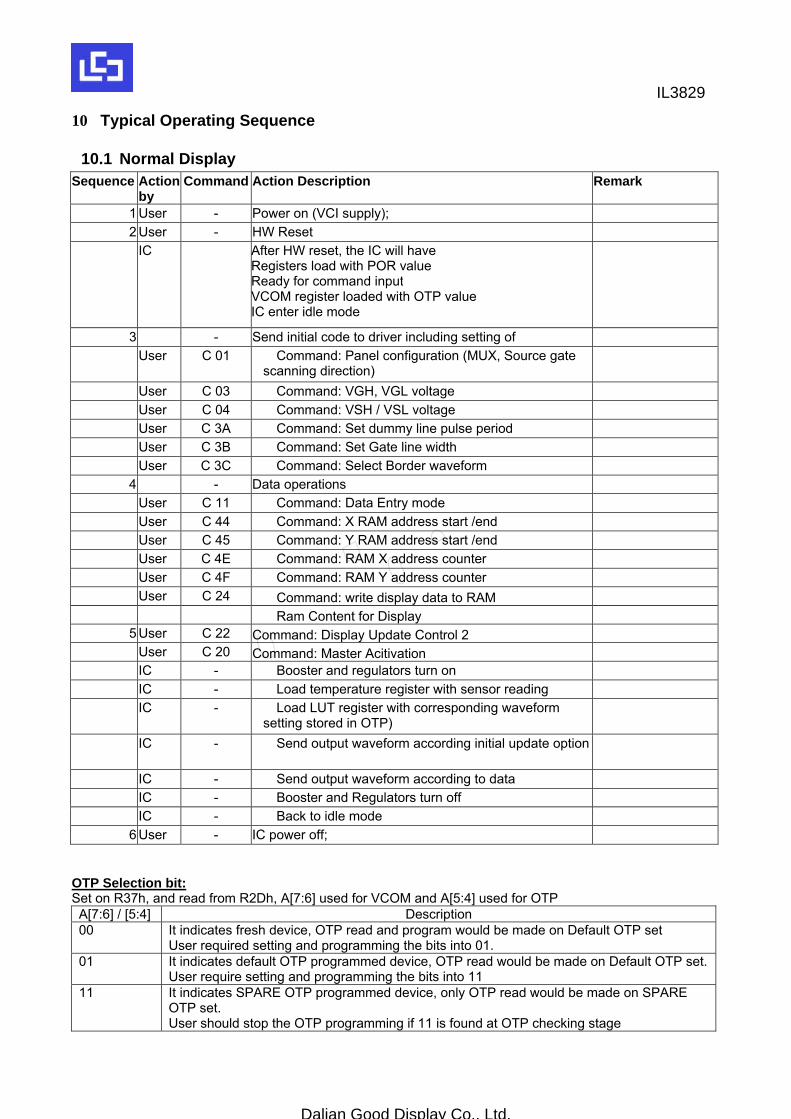
10 Typical Operating Sequence
10.1 Normal Display Sequence Action
by Command Action Description Remark
1 User - Power on (VCI supply); 2 User - HW Reset
IC After HW reset, the IC will have Registers load with POR value Ready for command input VCOM register loaded with OTP value IC enter idle mode
3 - Send initial code to driver including setting of User C 01 Command: Panel configuration (MUX, Source gate
scanning direction)
User C 03 Command: VGH, VGL voltage User C 04 Command: VSH / VSL voltage User C 3A Command: Set dummy line pulse period User C 3B Command: Set Gate line width
User C 3C Command: Select Border waveform 4 - Data operations
User C 11 Command: Data Entry mode User C 44 Command: X RAM address start /end User C 45 Command: Y RAM address start /end User C 4E Command: RAM X address counter User C 4F Command: RAM Y address counter User C 24 Command: write display data to RAM Ram Content for Display
5 User C 22 Command: Display Update Control 2 User C 20 Command: Master Acitivation
IC - Booster and regulators turn on IC - Load temperature register with sensor reading IC - Load LUT register with corresponding waveform
setting stored in OTP)
IC - Send output waveform according initial update option
IC - Send output waveform according to data IC - Booster and Regulators turn off IC - Back to idle mode
6 User - IC power off; OTP Selection bit: Set on R37h, and read from R2Dh, A[7:6] used for VCOM and A[5:4] used for OTP A[7:6] / [5:4] Description 00 It indicates fresh device, OTP read and program would be made on Default OTP set
User required setting and programming the bits into 01. 01 It indicates default OTP programmed device, OTP read would be made on Default OTP set.
User require setting and programming the bits into 11 11 It indicates SPARE OTP programmed device, only OTP read would be made on SPARE
OTP set. User should stop the OTP programming if 11 is found at OTP checking stage
IL3829
Dalian Good Display Co., Ltd.
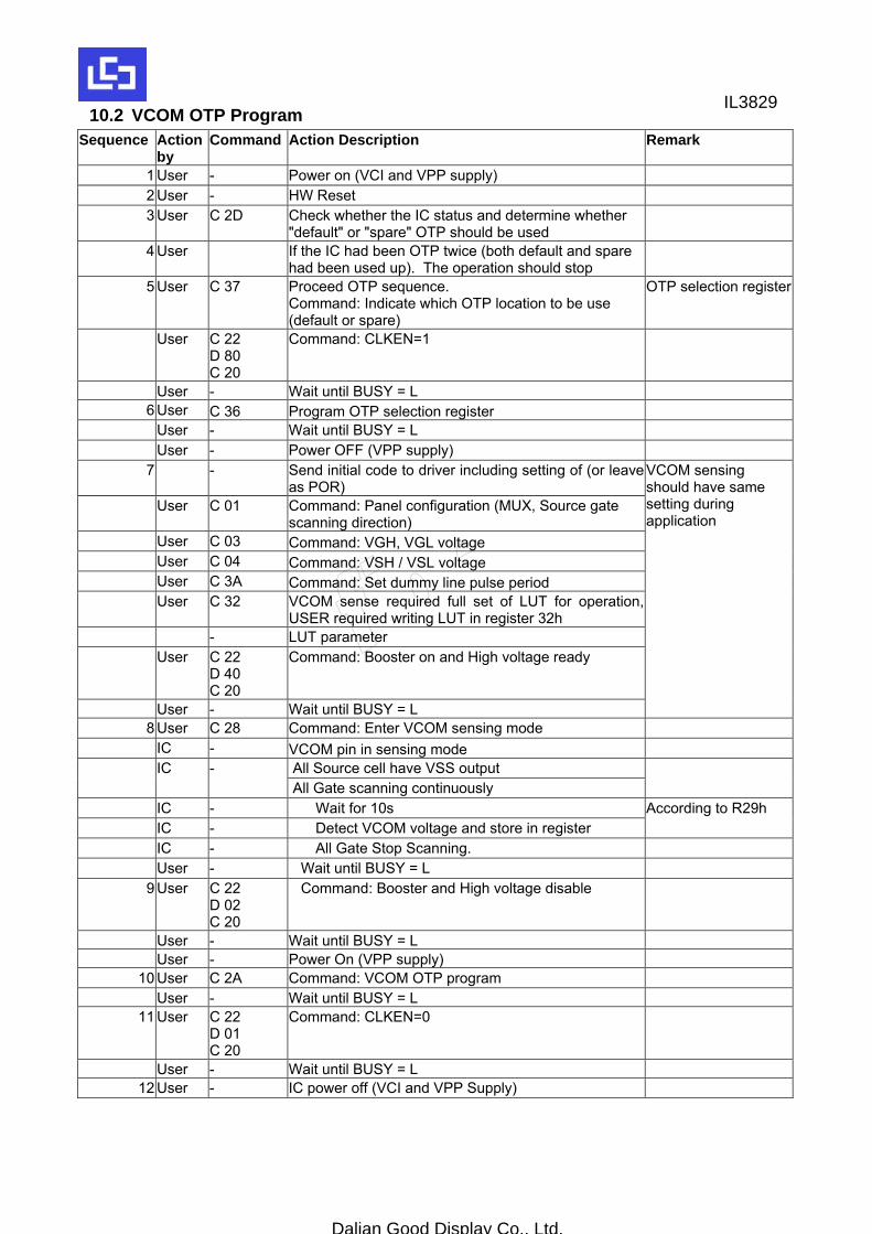
10.2 VCOM OTP Program Sequence Action
by Command Action Description Remark
1 User - Power on (VCI and VPP supply) 2 User - HW Reset 3 User C 2D Check whether the IC status and determine whether
"default" or "spare" OTP should be used
4 User If the IC had been OTP twice (both default and spare had been used up). The operation should stop
5 User C 37 Proceed OTP sequence. Command: Indicate which OTP location to be use (default or spare)
OTP selection register
User C 22 D 80 C 20
Command: CLKEN=1
User - Wait until BUSY = L 6 User C 36 Program OTP selection register
User - Wait until BUSY = L User - Power OFF (VPP supply)
7 - Send initial code to driver including setting of (or leave as POR)
User C 01 Command: Panel configuration (MUX, Source gate scanning direction)
User C 03 Command: VGH, VGL voltage User C 04 Command: VSH / VSL voltage User C 3A Command: Set dummy line pulse period User C 32
VCOM sense required full set of LUT for operation, USER required writing LUT in register 32h
- LUT parameter User C 22
D 40 C 20
Command: Booster on and High voltage ready
User - Wait until BUSY = L
VCOM sensing should have same setting during application
8 User C 28 Command: Enter VCOM sensing mode IC - VCOM pin in sensing mode
All Source cell have VSS output IC - All Gate scanning continuously
IC - Wait for 10s IC - Detect VCOM voltage and store in register
According to R29h
IC - All Gate Stop Scanning. User - Wait until BUSY = L
9 User C 22 D 02 C 20
Command: Booster and High voltage disable
User - Wait until BUSY = L User - Power On (VPP supply)
10 User C 2A Command: VCOM OTP program User - Wait until BUSY = L
11 User C 22 D 01 C 20
Command: CLKEN=0
User - Wait until BUSY = L 12 User - IC power off (VCI and VPP Supply)
IL3829
Dalian Good Display Co., Ltd.
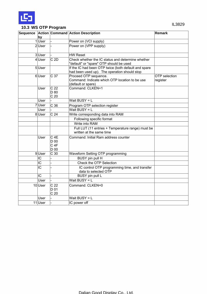
10.3 WS OTP Program Sequence Action
by Command Action Description Remark
1 User - Power on (VCI supply) 2 User - Power on (VPP supply)
3 User - HW Reset 4 User C 2D Check whether the IC status and determine whether
"default" or "spare" OTP should be used
5 User If the IC had been OTP twice (both default and spare had been used up). The operation should stop
6 User C 37 Proceed OTP sequence. Command: Indicate which OTP location to be use (default or spare)
OTP selection register
User C 22 D 80 C 20
Command: CLKEN=1
User - Wait BUSY = L 7 User C 36 Program OTP selection register
User - Wait BUSY = L 8 User C 24 Write corresponding data into RAM
Following specific format Write into RAM Full LUT (11 entries + Temperature range) must be
written at the same time
User C 4E D 00 C 4F D 00
Command: Initial Ram address counter
9 User C 30 Waveform Setting OTP programming IC - BUSY pin pull H
IC - Check the OTP Selection IC - IC control OTP programming time, and transfer
data to selected OTP
IC - BUSY pin pull L User - Wait BUSY = L
10 User C 22 D 01 C 20
Command: CLKEN=0
User - Wait BUSY = L 11 User - IC power off
IL3829
Dalian Good Display Co., Ltd.
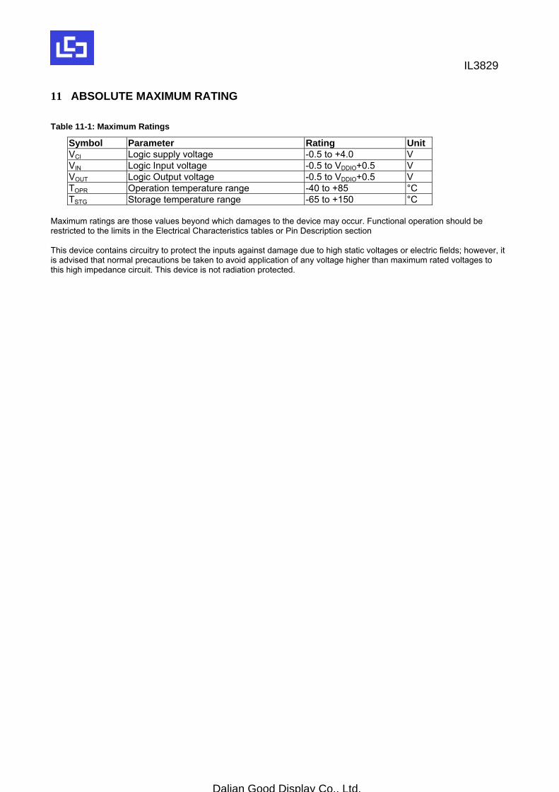
11 ABSOLUTE MAXIMUM RATING Table 11-1: Maximum Ratings
Symbol Parameter Rating Unit VCI Logic supply voltage -0.5 to +4.0 V VIN Logic Input voltage -0.5 to VDDIO+0.5 V VOUT Logic Output voltage -0.5 to VDDIO+0.5 V TOPR Operation temperature range -40 to +85 °C TSTG Storage temperature range -65 to +150 °C
Maximum ratings are those values beyond which damages to the device may occur. Functional operation should be restricted to the limits in the Electrical Characteristics tables or Pin Description section This device contains circuitry to protect the inputs against damage due to high static voltages or electric fields; however, it is advised that normal precautions be taken to avoid application of any voltage higher than maximum rated voltages to this high impedance circuit. This device is not radiation protected.
IL3829
Dalian Good Display Co., Ltd.
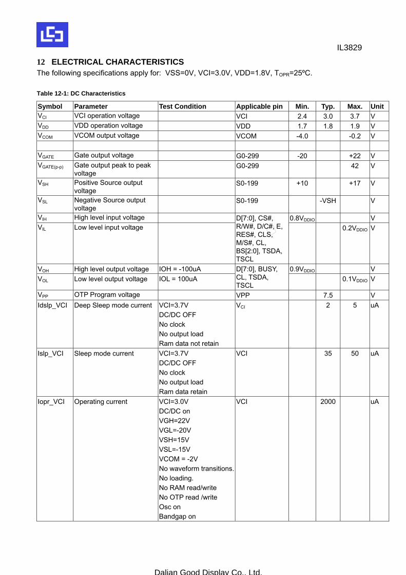
12 ELECTRICAL CHARACTERISTICS The following specifications apply for: VSS=0V, VCI=3.0V, VDD=1.8V, TOPR=25ºC. Table 12-1: DC Characteristics
Symbol Parameter Test Condition Applicable pin Min. Typ. Max. UnitVCI VCI operation voltage VCI 2.4 3.0 3.7 V VDD VDD operation voltage VDD 1.7 1.8 1.9 V VCOM VCOM output voltage VCOM -4.0 -0.2 V VGATE Gate output voltage G0-299 -20 +22 V VGATE(p-p) Gate output peak to peak
voltage G0-299 42 V
VSH Positive Source output voltage
S0-199 +10 +17 V
VSL Negative Source output voltage
S0-199 -VSH V
VIH High level input voltage 0.8VDDIO V VIL Low level input voltage
D[7:0], CS#, R/W#, D/C#, E, RES#, CLS, M/S#, CL, BS[2:0], TSDA, TSCL
0.2VDDIO V
VOH High level output voltage IOH = -100uA 0.9VDDIO V VOL Low level output voltage IOL = 100uA
D[7:0], BUSY, CL, TSDA, TSCL
0.1VDDIO V
VPP OTP Program voltage VPP 7.5 V Idslp_VCI Deep Sleep mode current VCI=3.7V
DC/DC OFF No clock No output load Ram data not retain
VCI 2 5
uA
Islp_VCI Sleep mode current VCI=3.7V DC/DC OFF No clock No output load Ram data retain
VCI 35 50
uA
Iopr_VCI Operating current VCI=3.0V DC/DC on VGH=22V VGL=-20V VSH=15V VSL=-15V VCOM = -2V No waveform transitions.No loading. No RAM read/write No OTP read /write Osc on Bandgap on
VCI 2000 uA
IL3829
Dalian Good Display Co., Ltd.
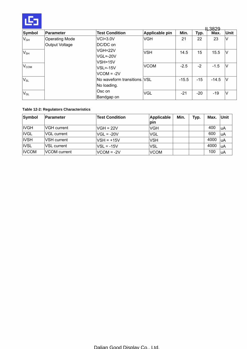
Symbol Parameter Test Condition Applicable pin Min. Typ. Max. UnitVGH VGH 21 22 23 V
VSH VSH 14.5 15 15.5 V
VCOM VCOM -2.5 -2 -1.5 V
VSL VSL -15.5 -15 -14.5 V
VGL
Operating Mode Output Voltage
VCI=3.0V DC/DC on VGH=22V VGL=-20V VSH=15V VSL=-15V VCOM = -2V No waveform transitions.No loading. Osc on Bandgap on
VGL -21 -20 -19 V
Table 12-2: Regulators Characteristics
Symbol Parameter Test Condition Applicable pin
Min. Typ. Max. Unit
IVGH VGH current VGH = 22V VGH 400 uA IVGL VGL current VGL = -20V VGL 600 uA IVSH VSH current VSH = +15V VSH 4000 uA IVSL VSL current VSL = -15V VSL 4000 uA IVCOM VCOM current VCOM = -2V VCOM 100 uA
IL3829
Dalian Good Display Co., Ltd.
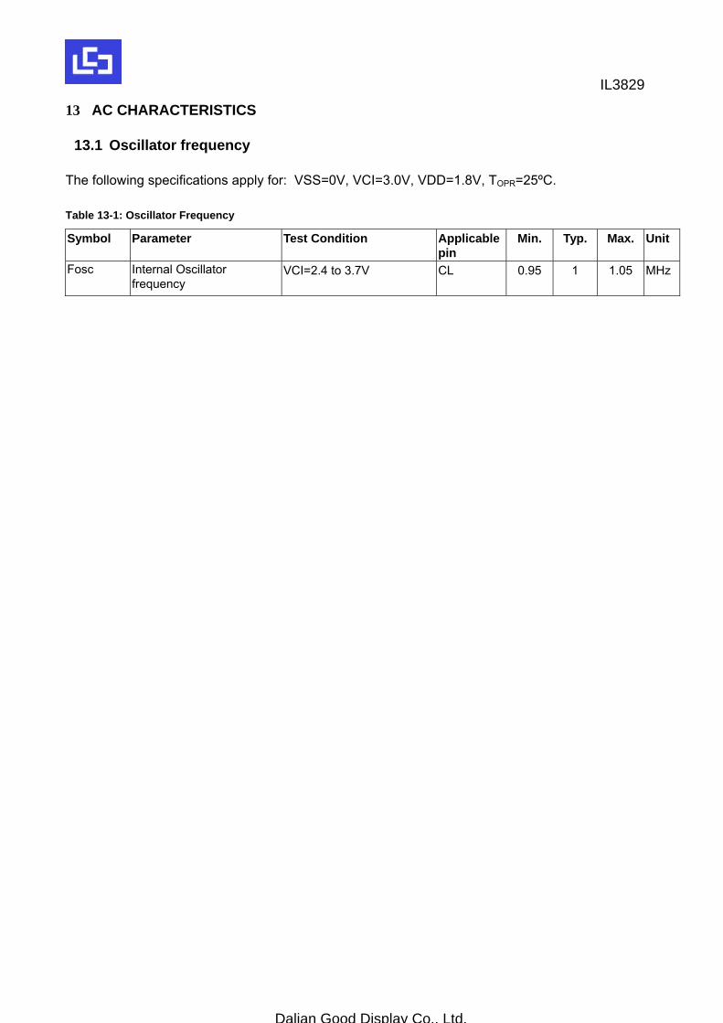
13 AC CHARACTERISTICS
13.1 Oscillator frequency The following specifications apply for: VSS=0V, VCI=3.0V, VDD=1.8V, TOPR=25ºC. Table 13-1: Oscillator Frequency
Symbol Parameter Test Condition Applicable pin
Min. Typ. Max. Unit
Fosc Internal Oscillator frequency
VCI=2.4 to 3.7V
CL 0.95 1 1.05 MHz
IL3829
Dalian Good Display Co., Ltd.
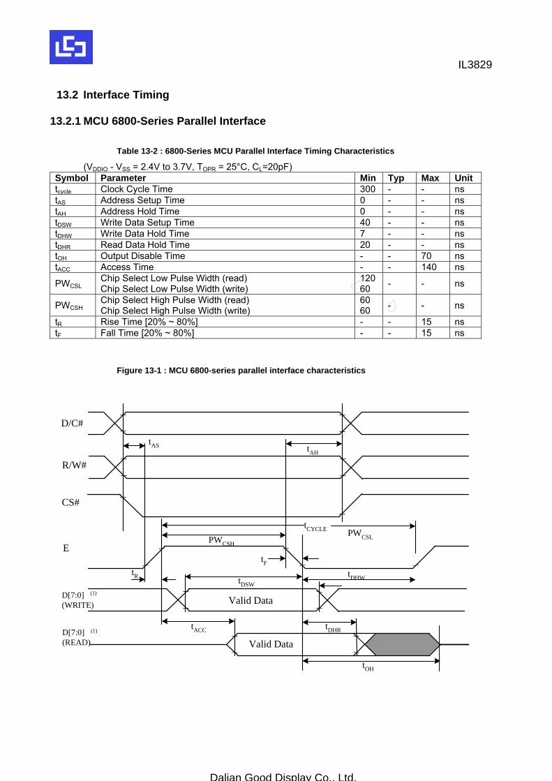
13.2 Interface Timing 13.2.1 MCU 6800-Series Parallel Interface
Table 13-2 : 6800-Series MCU Parallel Interface Timing Characteristics
(VDDIO - VSS = 2.4V to 3.7V, TOPR = 25°C, CL=20pF) Symbol Parameter Min Typ Max Unit tcycle Clock Cycle Time 300 - - ns tAS Address Setup Time 0 - - ns tAH Address Hold Time 0 - - ns tDSW Write Data Setup Time 40 - - ns tDHW Write Data Hold Time 7 - - ns tDHR Read Data Hold Time 20 - - ns tOH Output Disable Time - - 70 ns tACC Access Time - - 140 ns
PWCSL Chip Select Low Pulse Width (read) Chip Select Low Pulse Width (write)
12060 - - ns
PWCSH Chip Select High Pulse Width (read) Chip Select High Pulse Width (write)
60 60 - - ns
tR Rise Time [20% ~ 80%] - - 15 ns tF Fall Time [20% ~ 80%] - - 15 ns
Figure 13-1 : MCU 6800-series parallel interface characteristics
D[7:0] (WRITE)
(1)
D[7:0](READ)
(1)
CS#
E
R/W#
Valid Data
Valid Data
D/C#
tAS
tCYCLE
tDSW
tACC tDHR
tOH
tR
tAH
PWCSHPWCSL
tDHW
tF
IL3829
Dalian Good Display Co., Ltd.
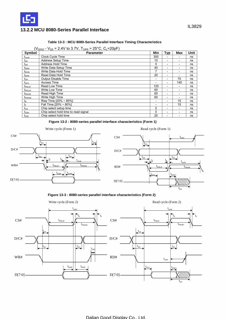
13.2.2 MCU 8080-Series Parallel Interface
Table 13-3 : MCU 8080-Series Parallel Interface Timing Characteristics
(VDDIO - VSS = 2.4V to 3.7V, TOPR = 25°C, CL=20pF) Symbol Parameter Min Typ Max Unittcycle Clock Cycle Time 300 - - ns tAS Address Setup Time 10 - - ns tAH Address Hold Time 0 - - ns tDSW Write Data Setup Time 40 - - ns tDHW Write Data Hold Time 7 - - ns tDHR Read Data Hold Time 20 - - ns tOH Output Disable Time - - 70 ns tACC Access Time - - 140 ns tPWLR Read Low Time 120 - - ns tPWLW Write Low Time 60 - - ns tPWHR Read High Time 60 - - ns tPWHW Write High Time 60 - - ns tR Rise Time [20% ~ 80%] - - 15 ns tF Fall Time [20% ~ 80%] - - 15 ns tCS Chip select setup time 0 - - ns tCSH Chip select hold time to read signal 0 - - ns tCSF Chip select hold time 20 - - ns
Figure 13-2 : 8080-series parallel interface characteristics (Form 1)
WR#
D[7:0]
tAS
D/C#
CS#
tCS
tAH
tPWLW
tcycle
tDSW tDHW
tPWHW
tCSF
RD#
D[7:0]
tAS
D/C#
CS#
tCS
tAH
tPWLR
tcycle
tPWHR
tCSH
tACC tDHR
tOH
tF tR tF tR
Write cycle (Form 1) Read cycle (Form 1)
Figure 13-3 : 8080-series parallel interface characteristics (Form 2)
WR#
D[7:0]
D/C#
CS#
tcycle
tPWLW
tPWHW
tFtR
tCS
tAS tAH tCSF
tDSW tDHW
RD#
D[7:0]
D/C#
CS#
tcycle
tPWLR
tPWHR
tFtR
tCS
tAS tAH
tACC tDHR
tOH
tCSH
Write cycle (Form 2) Read cycle (Form 2)
IL3829
Dalian Good Display Co., Ltd.
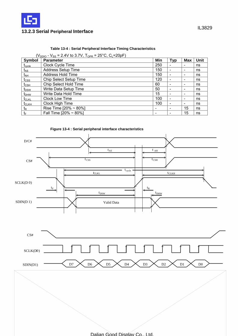
13.2.3 Serial Peripheral Interface
Table 13-4 : Serial Peripheral Interface Timing Characteristics
(VDDIO - VSS = 2.4V to 3.7V, TOPR = 25°C, CL=20pF) Symbol Parameter Min Typ Max Unit tcycle Clock Cycle Time 250 - - ns tAS Address Setup Time 150 - - ns tAH Address Hold Time 150 - - ns tCSS Chip Select Setup Time 120 - - ns tCSH Chip Select Hold Time 60 - - ns tDSW Write Data Setup Time 50 - - ns tDHW Write Data Hold Time 15 - - ns tCLKL Clock Low Time 100 - - ns tCLKH Clock High Time 100 - - ns tR Rise Time [20% ~ 80%] - - 15 ns tF Fall Time [20% ~ 80%] - - 15 ns
Figure 13-4 : Serial peripheral interface characteristics
t AHtAS
D/C#
Valid Data
tDHW
t CLKL
tDSW
t CLKH tcycle
t CSS tCSH
tF tR
SDIN(D 1 )
CS#
SCLK(D 0 )
D7SDIN(D1)
CS#
SCLK(D 0 )
D6 D5 D4 D3 D2 D1 D0
IL3829
Dalian Good Display Co., Ltd.
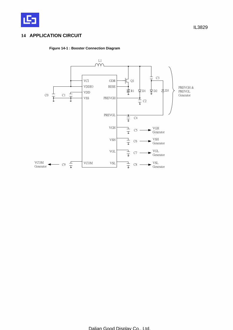
14 APPLICATION CIRCUIT
Figure 14-1 : Booster Connection Diagram
C3
C2
GDR
C6VSH VSHGenerator
C7VGL
C8VSL
VGL Generator
VSLGenerator
C9 VCOMVCOMGenerator
C1VDD
VDDIO
VCI
VSSC0
RESE
PREVGH
PREVGLC4
L1
Q1
R1 D1 D2 D3PREVGH & PREVGL Generator
VGHC5
VGHGenerator
IL3829
Dalian Good Display Co., Ltd.
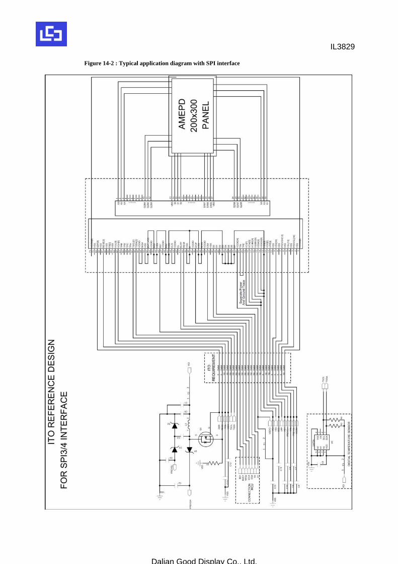
Figure 14-2 : Typical application diagram with SPI interface
IL3829
Dalian Good Display Co., Ltd.
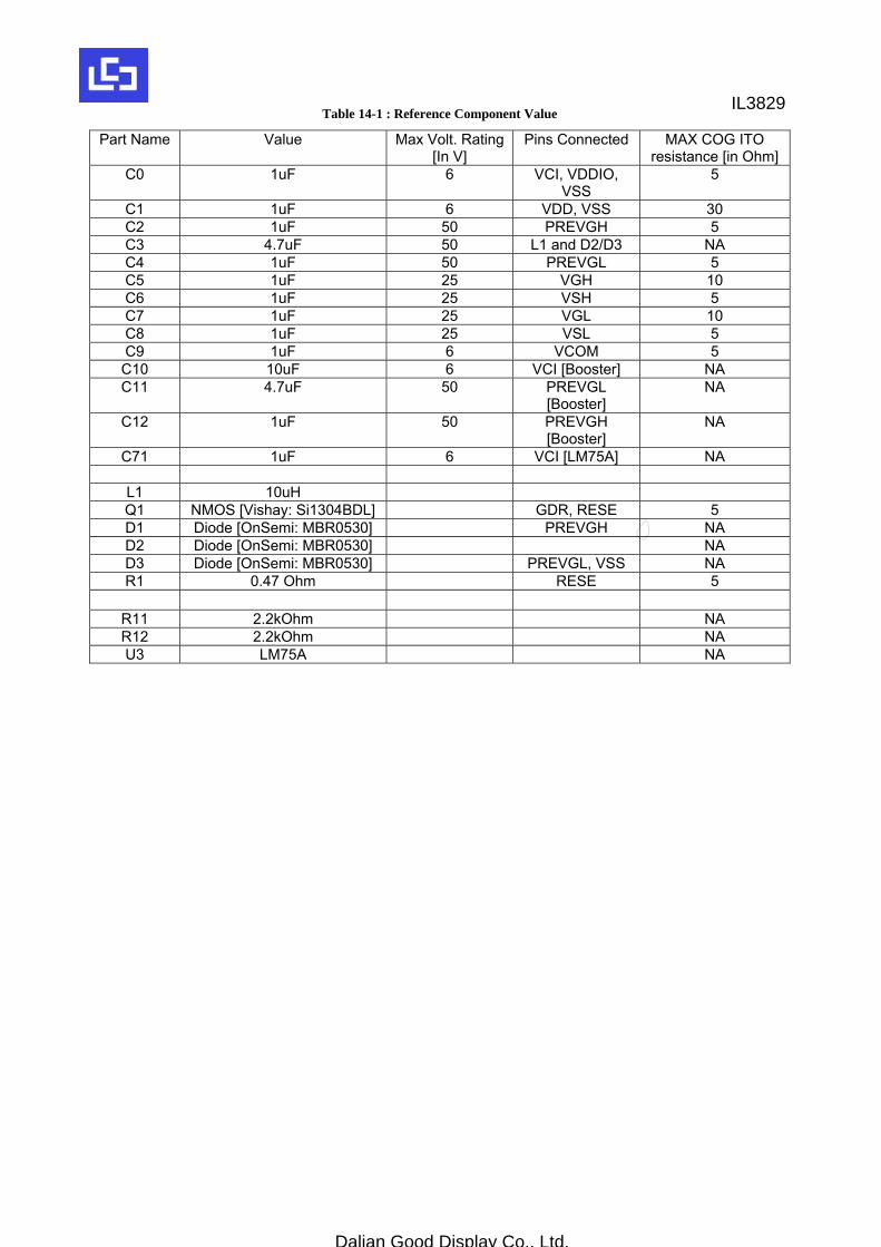
Table 14-1 : Reference Component Value
Part Name Value
Max Volt. Rating[In V]
Pins Connected MAX COG ITO resistance [in Ohm]
C0 1uF 6 VCI, VDDIO, VSS
5
C1 1uF 6 VDD, VSS 30 C2 1uF 50 PREVGH 5 C3 4.7uF 50 L1 and D2/D3 NA C4 1uF 50 PREVGL 5 C5 1uF 25 VGH 10 C6 1uF 25 VSH 5 C7 1uF 25 VGL 10 C8 1uF 25 VSL 5 C9 1uF 6 VCOM 5 C10 10uF 6 VCI [Booster] NA C11 4.7uF 50 PREVGL
[Booster] NA
C12 1uF 50 PREVGH [Booster]
NA
C71 1uF 6 VCI [LM75A] NA
L1 10uH Q1 NMOS [Vishay: Si1304BDL] GDR, RESE 5 D1 Diode [OnSemi: MBR0530] PREVGH NA D2 Diode [OnSemi: MBR0530] NA D3 Diode [OnSemi: MBR0530] PREVGL, VSS NA R1 0.47 Ohm RESE 5
R11 2.2kOhm NA R12 2.2kOhm NA U3 LM75A NA
IL3829
Dalian Good Display Co., Ltd.