Embed Size (px)
Citation preview
Weapons and Protection
SE-147 25 Tumba
FOI-R--0541--SEJune 2002
Technical report
Adam Lindblom
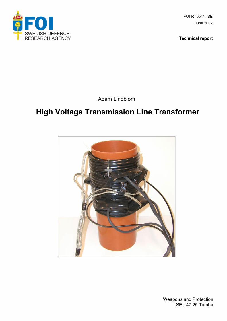
High Voltage Transmission Line Transformer
SWEDISH DEFENCE RESEARCH AGENCY FOI-R--0541--SE
June 2002Weapons and Protection SE-147 25 Tumba
Technical report
High Voltage Transmission Line Transformer
2
Issuing organisation Report number, ISRN Report type FOI – Swedish Defence Research Agency FOI-R--0541--SE Technical report
Research area code 6. Electronic Warfare Month year Project no. June 2002 E2013 Customers code 5. Contracted Research Sub area code
Weapons and Protection SE-147 25 Tumba
61 Electronic Warfare, Electromagnetic Weapons Authors Project manager Adam Lindblom Sten E Nyholm Approved by
Torgny Carlsson
Scientifically and technically responsible Report title High Voltage Transmission Line Transformer
Abstract One way to achieve high voltage is to use a step-up transformer. This report describes the design and the construction of a transmission line transformer using a high voltage cable for usage in the high-voltage system TTHPM at FOI. Experimental results and equivalent electric circuit simulation models are presented. The measured input and output signals are analysed with parametric models giving the possibility to calculate step responses and Bode plots. A transmission line transformer works in the same way as an ordinary transformer. The input is transformed to the desired output using a step up or a step down configuration. The configuration described here uses a cable designed to withstand high voltage stress, the cable has a semi-conducting layer covering the inner copper wires and the outer plastic shielding. The design has proven to have a high coupling factor even though it uses an air core. This type of transformer is useful in applications where weight is an important factor, another advantage is the simple design and that it can be made to a low cost.
Keywords Transmission line transformer, coaxial cable, high voltage
Further bibliographic information Language English
ISSN 1650-1942 Pages: 59
Price acc. to pricelist
Security classification
3
Utgivare Rapportnummer, ISRN Klassificering Totalförsvarets Forskningsinstitut – FOI FOI-R--0541--SE Teknisk rapport
Forskningsområde 6. Telekrig Månad, år Projektnummer Juni 2002 E2013 Verksamhetsgren 5. Uppdragsfinansierad verksamhet Delområde
Vapen och skydd 147 25 Tumba
61 Telekrigföring med EM-vapen och skydd Författare/redaktör Projektledare Adam Lindblom Sten E Nyholm Godkänd av Torgny Carlsson Uppdragsgivare/kundbeteckning Tekniskt och/eller vetenskapligt ansvarig Rapportens titel (i översättning) Transmissionsledningstransformator med högspänningskabel.
Sammanfattning (högst 200 ord) Ett sätt att erhålla högspänning är att använda en transformator. I denna projektrapport beskrivs konstruktionen av en transmissionsledningstransformator baserad på en högspänningskabel. Denna transformator har sedan används i FOIs högspänningssystem TTHPM. Experimentella resultat och simulering med ekvivalenta elektriska kretsar presenteras. Uppmätta insignaler och utsignaler analyseras med hjälp av parametriska modeller och från dessa presenteras stegsvar och Bode diagram. En transformator baserad på koaxialkabel fungerar i princip på samma sätt som en vanlig transformator. Insignalen kan förändras till önskvärd utsignal genom att använda en upp- eller nertransformering. I denna konstruktion används en högspännigskabel med ett resistivt skikt på innerledaren och det yttre plastlagret. Tester har visat att transformatorn har hög kopplingsfaktor trots att den använder luftkärna. Den lämpar sig väl för användningsområden där låg vikt prioriteras, dessutom är konstruktionen relativt enkel att genomföra till låg kostnad.
Nyckelord Transmissionsledningstransformator, koaxialkabel, högspänning.
Övriga bibliografiska uppgifter Språk Engelska
ISSN 1650-1942 Antal sidor: 59
Distribution enligt missiv Pris: Enligt prislista
Sekretess
4
Contents
1 Introduction .................................................................................................. 6
2 Electromagnetic field theory ....................................................................... 7
2.1 Stokes’ theorem.......................................................................................................... 7
2.2 Gauss theorem............................................................................................................ 7
2.3 Ampère’s law ............................................................................................................. 8
2.4 The magnetic induction.............................................................................................. 8
2.5 The magnetic flux....................................................................................................... 9
2.6 The magnetic vector potential .................................................................................... 9
2.7 Faraday’s law of electromagnetic induction ............................................................ 10
2.8 Mutual inductance .................................................................................................... 11
2.9 Self inductance ......................................................................................................... 13
3 Transformer theory.................................................................................... 14
3.1 The ideal transformer ............................................................................................... 14
3.2 The real transformer ................................................................................................. 15
3.3 Leakage inductance .................................................................................................. 17
3.4 Modified coupling theory......................................................................................... 18
3.5 Capacitance .............................................................................................................. 21
3.6 Transmission line transformer.................................................................................. 21
4 Construction of transmission line transformer ....................................... 24
4.1 Test transformer ....................................................................................................... 24
4.2 Semicon cable .......................................................................................................... 24
4.3 Making the semicon cable coaxial ........................................................................... 25
4.4 Coil parameters ........................................................................................................ 25
4.5 Helical geometry ...................................................................................................... 27
4.6 Electrical breakdown prevention.............................................................................. 28
5 Measurements ............................................................................................. 29
5.1 Inductance measurement .......................................................................................... 29
5.2 Measured compared to calculated inductance.......................................................... 31
5.3 Transformer analysis set-up ..................................................................................... 32

5
5.4 Transfer function analysis ........................................................................................ 33
5.5 Electric circuit simulation models............................................................................ 35
5.6 Power and Energy .................................................................................................... 37
6 Magnetic field simulation .......................................................................... 39
6.1 Current density ......................................................................................................... 39
6.2 Solenoidal field appearance ..................................................................................... 39
7 The high voltage system............................................................................. 41
8 High voltage measurement ........................................................................ 44
9 High voltage results .................................................................................... 46
10 Conclusions .............................................................................................. 54
10.1 Summary .................................................................................................................. 54
10.2 Suggestions for improvements ................................................................................. 54
References .......................................................................................................... 55
Appendix A ........................................................................................................ 57
6
1 Introduction This technical report presents a Master thesis work performed at FOI Grindsjön Research Centre for Luleå University of Technology in cooperation with Uppsala University. Supervisor at FOI has been Anders Larsson. The main project goal is to investigate how a pulsed high voltage capacitor system responds when a transformer is connected to it. Since the input in this case is a single pulse the use of a pulse transformer is investigated. The main difference between a pulsed and a continuos power source is that the maximum voltage stress can be pushed beyond the dielectric breakdown limits, though this factor is very dependent of the pulse length. The ohmic heating existing in continuos transformer systems will neither be a problem. The main design problem will be electrical breakdown prevention. Therefore the use of a high voltage cable applied as winding in the transformer is investigated. The design of the cable transformer with coaxial windings originates from Hans Bernhoff and Jan Isberg, Division for Electricity and Lightning Research, Uppsala University. Most of the analysis software and the measured pulses can be found on a Compact Disc since the material is too extensive to be enclosed in an appendix. This work is a part of the HPM weapons programme at FOI Grindsjön Research Centre and is supported by the Swedish Armed Forces.
7
2 Electromagnetic field theory The main source of information for this chapter is collected from Wangsness [1].
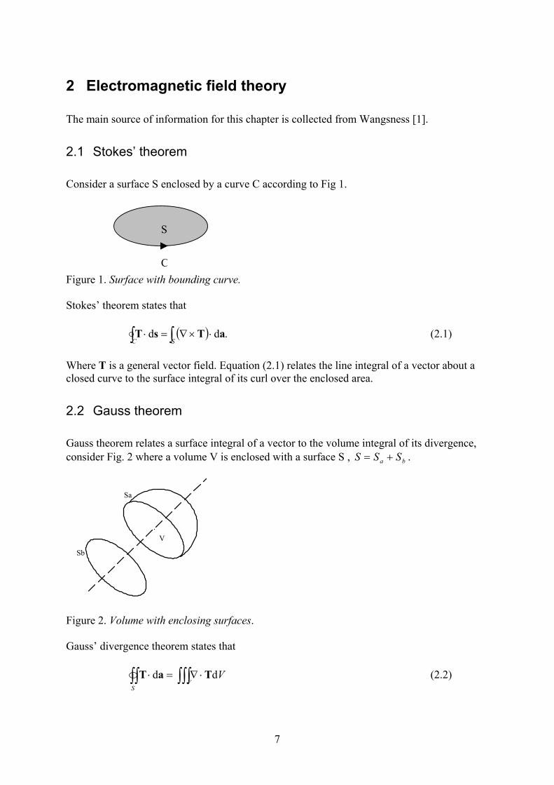
2.1 Stokes’ theorem Consider a surface S enclosed by a curve C according to Fig 1.
Figure 1. Surface with bounding curve. Stokes’ theorem states that
( ) .dd ∫∫ ⋅×∇=⋅SC
aTsT (2.1)
Where T is a general vector field. Equation (2.1) relates the line integral of a vector about a closed curve to the surface integral of its curl over the enclosed area.
2.2 Gauss theorem Gauss theorem relates a surface integral of a vector to the volume integral of its divergence, consider Fig. 2 where a volume V is enclosed with a surface S , ba SSS += .
Figure 2. Volume with enclosing surfaces. Gauss’ divergence theorem states that
∫∫∫∫∫ ⋅∇=⋅V
S
Vdd TaT (2.2)
C
S
Sb
Sa
V
8
2.3 Ampère’s law The force between two idealized circuits C and C’, carrying steady filamentary currents I and I’ is expressed as
CC →'F . The circuits are idealized in the sense that the sources are not
included in Figure 3. The basic experimental law that gives the total force on C due to C’ can be written as
( )∫ ∫
×′′×=
→ C CCC RI
'' 20
ˆddI4
RssFπ
µ (2.3)
where µ0 is the permeability of free space. R is the unit vector in the R direction
.ˆRR
rrRR′−
== (2.4)
Equation (2.3) has the form of a double line integral, each of which is taken over the corresponding circuit.
Figure 3. Relations between two circuits as used to state Ampère’s law
2.4 The magnetic induction The magnetic induction describes the force interaction between currents in the same manner as the electric field describes the interaction between charges. Equation (2.3) can be rewritten as
( )∫ ∫
×′′×=
→ C CCC RI
'' 20
ˆd4
dI RssFπ
µ (2.5)
The quantity in parentheses is represented by )(rB , and combined with (2.4) gives
( ).d4
)(' 3
0 ∫×′′
=C R
I RsrBπ
µ (2.6)
R
rr'
O
I
ds' ds
CC'
I '
R
9
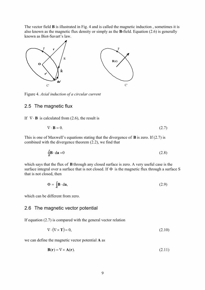
The vector field B is illustrated in Fig. 4 and is called the magnetic induction , sometimes it is also known as the magnetic flux density or simply as the B-field. Equation (2.6) is generally known as Biot-Savart’s law.
Figure 4. Axial induction of a circular current
2.5 The magnetic flux If B⋅∇ is calculated from (2.6), the result is
.0=⋅∇ B (2.7) This is one of Maxwell’s equations stating that the divergence of B is zero. If (2.7) is combined with the divergence theorem (2.2), we find that
0d∫ =⋅S
aB (2.8)
which says that the flux of B through any closed surface is zero. A very useful case is the surface integral over a surface that is not closed. If Φ is the magnetic flux through a surface S that is not closed, then
,d∫ ⋅=ΦS
aB (2.9)
which can be different from zero.
2.6 The magnetic vector potential If equation (2.7) is compared with the general vector relation
( ) ,0=×∇⋅∇ T (2.10) we can define the magnetic vector potential A as
).()( rArB ×∇= (2.11)
r'R
r
O
I'
ds'
^
R
r'
r
O
I'
ds'
I'I'
B(r)
C' C'
10
This step requires some lengthy calculations that the interested reader may find in Wangsness [1]. The magnetic flux Φ can be expressed in terms of the vector potential A , if Stoke’s theorem (2.1) is combined with (2.11), ( ) ∫∫ ⋅=⋅×∇=Φ
CS.dd sAaA (2.12)
This equation shows that the flux can be calculated as the line integral of A around the curve bounding the surface. Using (2.11) the vector potential is expressed as
.d4
)('
0 ∫′′
=C R
I srAπ
µ (2.13)
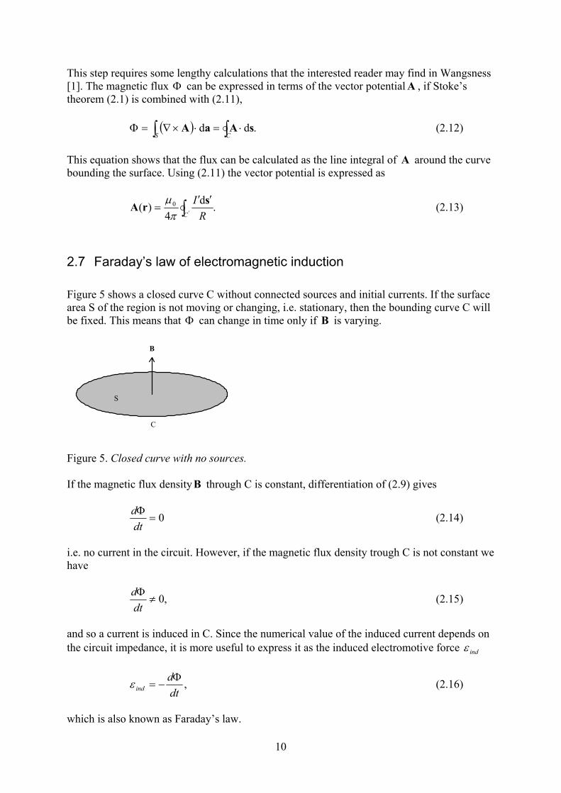
2.7 Faraday’s law of electromagnetic induction Figure 5 shows a closed curve C without connected sources and initial currents. If the surface area S of the region is not moving or changing, i.e. stationary, then the bounding curve C will be fixed. This means that Φ can change in time only if B is varying.
Figure 5. Closed curve with no sources. If the magnetic flux density B through C is constant, differentiation of (2.9) gives
0=Φ
dtd (2.14)
i.e. no current in the circuit. However, if the magnetic flux density trough C is not constant we have
,0≠Φ
dtd (2.15)
and so a current is induced in C. Since the numerical value of the induced current depends on the circuit impedance, it is more useful to express it as the induced electromotive force indε
,dtd
indΦ
−=ε (2.16)
which is also known as Faraday’s law.
S
C
B
11
From electrostatics we know that the electric field 0=E inside a metallic conductor for a completely static case. With moving charges in the conductor i.e. a current, we no longer have a static case and 0≠E within the wire. If the total work qW is done on charge q as it goes around the closed path C, then the ratio between work and charge is the electromotive force ε or simply the emf and we have
.q
Wq=ε (2.17)
From the definition of the electric field E we know that the force on charge q is
.EF q= (2.18) Further, the work done by the force around a closed path C becomes
.∫ ⋅=C qq dW sF (2.19)
Now if (2.17) is combined with (2.18) and (2.19) we get the emf as
.∫ ⋅=C
dsEε (2.20)
Hence, if a current produced by the induction flows in the conductor then 0≠E , we can then combine (2.16) and (2.20) to
,dtdd
C indΦ
−=⋅∫ sE (2.21)
which is the integral form of Faraday’s law.
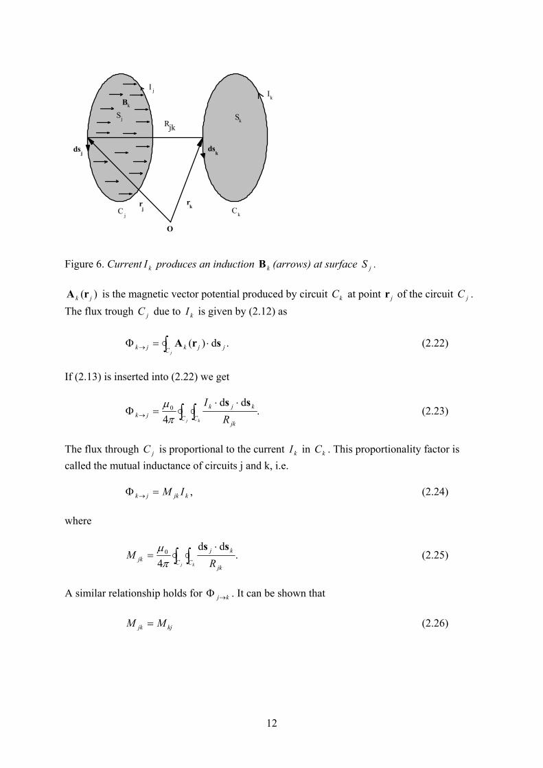
2.8 Mutual inductance Consider the two filamentary circuits illustrated in Fig. 6 (similar to Fig. 3), where
kjjkR rr −= since kjjk rrR −= . The current kI in Fig. 6 will produce an induction kB at
each point of the surface jS enclosed by jC and also a flux jk→Φ .
12
rr
O
I
ds ds
CC
I
Rjk
kj
j
j k
k
j k
SSkj
Bk
Figure 6. Current kI produces an induction kB (arrows) at surface jS .
)( jk rA is the magnetic vector potential produced by circuit kC at point jr of the circuit jC . The flux trough jC due to kI is given by (2.12) as
∫ ⋅=Φ →jC jjkjk .d)( srA (2.22)
If (2.13) is inserted into (2.22) we get
.dd
40 ∫ ∫
⋅⋅=Φ →
j kC Cjk
kjkjk R
I ssπ
µ (2.23)
The flux through jC is proportional to the current kI in kC . This proportionality factor is called the mutual inductance of circuits j and k, i.e.
,kjkjk IM=Φ → (2.24) where
.dd
40 ∫ ∫
⋅=
j kC Cjk
kjjk R
Mss
πµ
(2.25)
A similar relationship holds for kj→Φ . It can be shown that
kjjk MM = (2.26)
13
2.9 Self inductance The current in the circuit jC also produces a flux jj→Φ through itself, this factor of proportionality is called the self inductance or simply the inductance and is given by
,jjjjj IL=Φ → (2.27) where
∫ ∫⋅
=j jC C
jj
jjjj R
L'dd
40 ssπ
µ (2.28)
The double integral is taken twice [1] over the same circuit and, jds , jd 's are separate line elements of jC . However, this will not work for true filamentary currents of zero thickness because when jds and jd 's coincide 0=jjR and the integral diverges. The correct way to solve for the self inductance is to use (2.27) as the ratio of flux to current. However, this requires the knowledge of jj→Φ .
14
3 Transformer theory The transformer theory presented in this section is mainly collected from Cheng [2]. A transformer is a device that can transform three important electrical quantities namely • Voltage • Current • Impedance The usual configuration of a transformer is two or more coils that are coupled magnetically through a common core, where the input side is called the primary winding and the output the secondary winding. The core may contain ferromagnetic material.
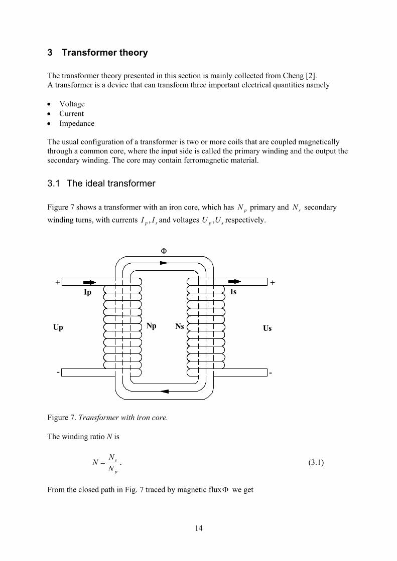
3.1 The ideal transformer Figure 7 shows a transformer with an iron core, which has pN primary and sN secondary winding turns, with currents sp II , and voltages sp UU , respectively.
NsNp
Ip Is+
-
+
-
Up Us
Φ
Figure 7. Transformer with iron core. The winding ratio N is
.p
s
NN
N = (3.1)
From the closed path in Fig. 7 traced by magnetic flux Φ we get
15
Φ=−AlININ sspp µ
(3.2)
where l is the core length and µ the permeability and A the cross-sectional area. In the ideal transformer ∞→µ and (3.2) becomes
.p
s
s
p
NN
II
= (3.3)
From Faraday’s law (2.16) we get
.dtdNU ppΦ
⋅= (3.4)
If it is assumed that the same flux Φ passes through the primary and secondary winding
.dtdNU ssΦ
⋅= (3.5)
Further, (3.4) divided by (3.5) gives the relation
s
p
s
p
NN
UU
= (3.6)
If the secondary coil is connected to a purely resistive load, then it can only remove energy from the magnetic field, but if the resistance is replaced by a reactance, then at some time during the voltage cycle the direction of energy transfer is reversed [3]. The impedance sZ as seen by the source connected to the primary is
.2
ss
pp Z
NN
Z ⋅
= (3.7)
3.2 The real transformer Referring to (3.2) we may write the magnetic flux relations for the primary and secondary windings as
)( 2sspppp INNIN
lAN −=Φ
µ (3.8)
and also
).( 2sspsps ININN
lAN −=Φ
µ (3.9)
16
Once again we assume that the same flux Φ passes both circuits. Further, using (3.8) and (3.9) in (3.4) and (3.5) we obtain the system
dtdI
Mdt
dILU sp
pp −= (3.10)
dtdI
Ldt
dIMU s
sp
s −= (3.11)
where
2pp N
lAL µ
= (3.12)
2ss N
lAL µ
= (3.13)
.sp NNlAM µ
= (3.14)
pL and sL are the self-inductance of the primary and the secondary winding respectively,
while M is the mutual inductance between the two circuits. Since equations (3.12), (3.13) and (3.14) assumes no leakage flux the calculated inductances will be too high. The ideal transformer has no leakage flux and
sp LLM = (3.15) However, in the real transformer we have [1], [2], [3], [12]
sp LLkM = , 1<k (3.16) where k is called the coupling coefficient. Another way to calculate the self inductance of a helical coil is to use
22
10910
nnn
nn N
lRR
L+
=µπ
(3.17)
this is the Wheeler’s formula [14] where n is referred to as primary and secondary index. Equation (3.17) gives an approximate inductance estimation, if the core length to winding radius has the ratio
,54
>n
n
Rl
(3.18)
17
where nl is the solenoid length and nR is the winding radius. The constants in the denominator (3.17) compensate for field changes at the boundarys of the solenoid as well as for some leakage flux. Note that the presumption ∞→µ for an ideal transformer also implies infinite inductance. The real transformer losses can be summarised accordingly, • the existence of leakage flux 1<k • finite inductance • nonzero winding resistance • hysteresis and eddy current losses (magnetic materials)
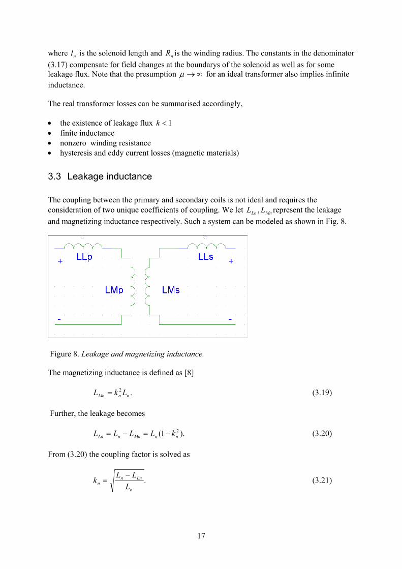
3.3 Leakage inductance The coupling between the primary and secondary coils is not ideal and requires the consideration of two unique coefficients of coupling. We let MnLn LL , represent the leakage and magnetizing inductance respectively. Such a system can be modeled as shown in Fig. 8.
Figure 8. Leakage and magnetizing inductance. The magnetizing inductance is defined as [8]
.2nnMn LkL = (3.19)
Further, the leakage becomes
).1( 2nnMnnLn kLLLL −=−= (3.20)
From (3.20) the coupling factor is solved as
.n
Lnnn L
LLk
−= (3.21)
18
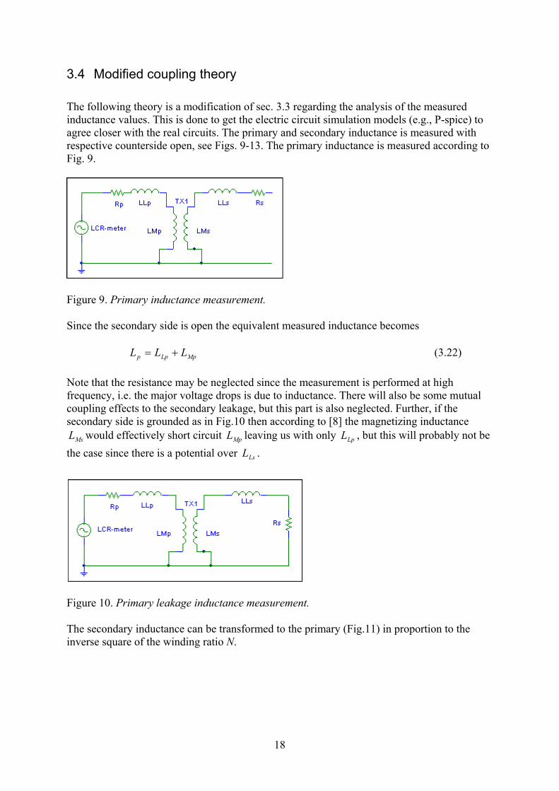
3.4 Modified coupling theory The following theory is a modification of sec. 3.3 regarding the analysis of the measured inductance values. This is done to get the electric circuit simulation models (e.g., P-spice) to agree closer with the real circuits. The primary and secondary inductance is measured with respective counterside open, see Figs. 9-13. The primary inductance is measured according to Fig. 9.
Figure 9. Primary inductance measurement. Since the secondary side is open the equivalent measured inductance becomes
MpLpp LLL += (3.22) Note that the resistance may be neglected since the measurement is performed at high frequency, i.e. the major voltage drops is due to inductance. There will also be some mutual coupling effects to the secondary leakage, but this part is also neglected. Further, if the secondary side is grounded as in Fig.10 then according to [8] the magnetizing inductance
MsL would effectively short circuit MpL leaving us with only LpL , but this will probably not be the case since there is a potential over LsL .
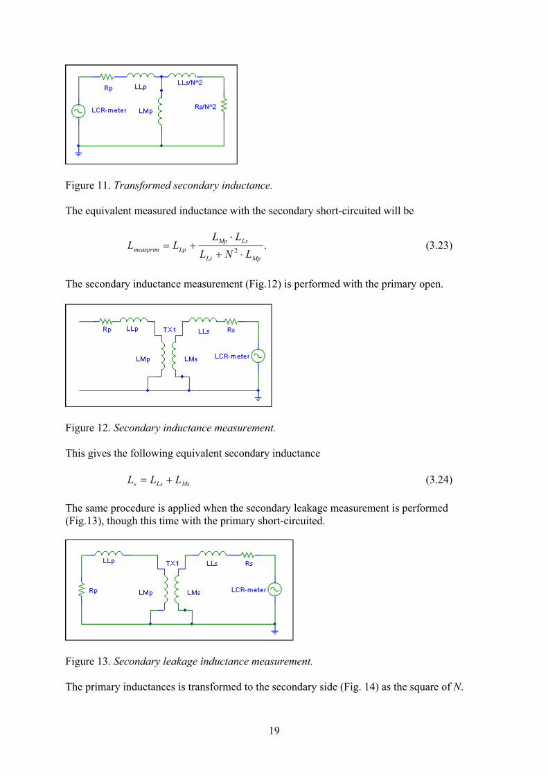
Figure 10. Primary leakage inductance measurement. The secondary inductance can be transformed to the primary (Fig.11) in proportion to the inverse square of the winding ratio N.
19
Figure 11. Transformed secondary inductance. The equivalent measured inductance with the secondary short-circuited will be
.2MpLs
LsMpLpmeasprim LNL
LLLL
⋅+
⋅+= (3.23)
The secondary inductance measurement (Fig.12) is performed with the primary open.
Figure 12. Secondary inductance measurement. This gives the following equivalent secondary inductance
MsLss LLL += (3.24) The same procedure is applied when the secondary leakage measurement is performed (Fig.13), though this time with the primary short-circuited.
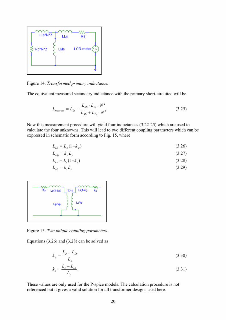
Figure 13. Secondary leakage inductance measurement. The primary inductances is transformed to the secondary side (Fig. 14) as the square of N.
20
Figure 14. Transformed primary inductance. The equivalent measured secondary inductance with the primary short-circuited will be
2
2
sec NLLNLL
LLLpMs
LpMsLsmeas ⋅+
⋅⋅+= (3.25)
Now this measurement procedure will yield four inductances (3.22-25) which are used to calculate the four unknowns. This will lead to two different coupling parameters which can be expressed in schematic form according to Fig. 15, where
)1( ppLp kLL −= (3.26)
ppMp LkL = (3.27) )1( ssLs kLL −= (3.28)
ssMs LkL = (3.29)
Figure 15. Two unique coupling parameters. Equations (3.26) and (3.28) can be solved as
p
Lppp L
LLk
−= (3.30)
.s
Lsss L
LLk
−= (3.31)
These values are only used for the P-spice models. The calculation procedure is not referenced but it gives a valid solution for all transformer designs used here.
21
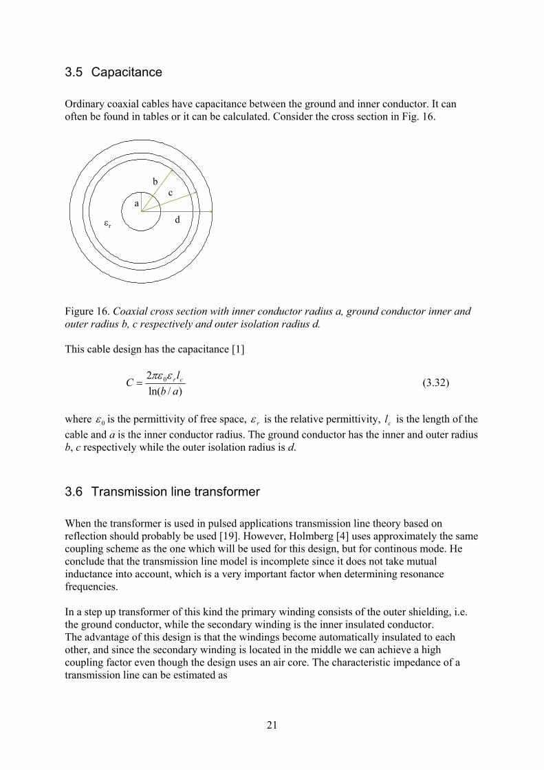
3.5 Capacitance Ordinary coaxial cables have capacitance between the ground and inner conductor. It can often be found in tables or it can be calculated. Consider the cross section in Fig. 16.
Figure 16. Coaxial cross section with inner conductor radius a, ground conductor inner and outer radius b, c respectively and outer isolation radius d. This cable design has the capacitance [1]
)/ln(2 0
abl
C crεπε= (3.32)
where 0ε is the permittivity of free space, rε is the relative permittivity, cl is the length of the cable and a is the inner conductor radius. The ground conductor has the inner and outer radius b, c respectively while the outer isolation radius is d.
3.6 Transmission line transformer When the transformer is used in pulsed applications transmission line theory based on reflection should probably be used [19]. However, Holmberg [4] uses approximately the same coupling scheme as the one which will be used for this design, but for continous mode. He conclude that the transmission line model is incomplete since it does not take mutual inductance into account, which is a very important factor when determining resonance frequencies. In a step up transformer of this kind the primary winding consists of the outer shielding, i.e. the ground conductor, while the secondary winding is the inner insulated conductor. The advantage of this design is that the windings become automatically insulated to each other, and since the secondary winding is located in the middle we can achieve a high coupling factor even though the design uses an air core. The characteristic impedance of a transmission line can be estimated as
a
bc
dεr
22
CLZ ≈0 (3.34)
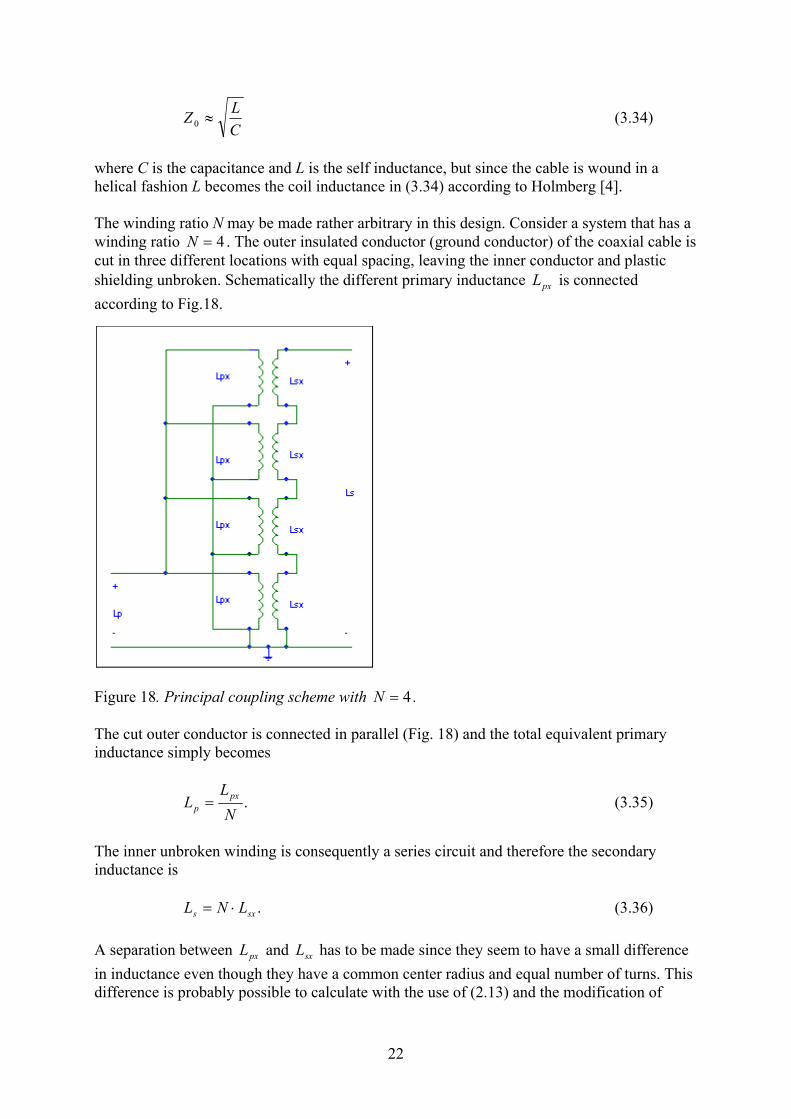
where C is the capacitance and L is the self inductance, but since the cable is wound in a helical fashion L becomes the coil inductance in (3.34) according to Holmberg [4]. The winding ratio N may be made rather arbitrary in this design. Consider a system that has a winding ratio 4=N . The outer insulated conductor (ground conductor) of the coaxial cable is cut in three different locations with equal spacing, leaving the inner conductor and plastic shielding unbroken. Schematically the different primary inductance pxL is connected according to Fig.18.
Figure 18. Principal coupling scheme with 4=N . The cut outer conductor is connected in parallel (Fig. 18) and the total equivalent primary inductance simply becomes
.N
LL px
p = (3.35)
The inner unbroken winding is consequently a series circuit and therefore the secondary inductance is
.sxs LNL ⋅= (3.36) A separation between pxL and sxL has to be made since they seem to have a small difference in inductance even though they have a common center radius and equal number of turns. This difference is probably possible to calculate with the use of (2.13) and the modification of

23
filamentary currents to a current density that varies with frequency in the cross-section of the windings. However, this seem to become very complicated. To simplify let’s call it x and
.pxsx LxL ⋅= (3.37) Then if (3.35), (3.36) and (3.37) are combined, we have
.2ps LxNL = (3.38)
During construction this winding ratio N was slightly modified since the primary terminal distance according to Fig. 21 had to be taken into account. Thus N is not necessarily a rational number.
24
4 Construction of transmission line transformer Two transformers have been constructed. The first one was made of a commercial RG-58 coaxial cable while the second high voltage transformer was made with a special cable from ABB.
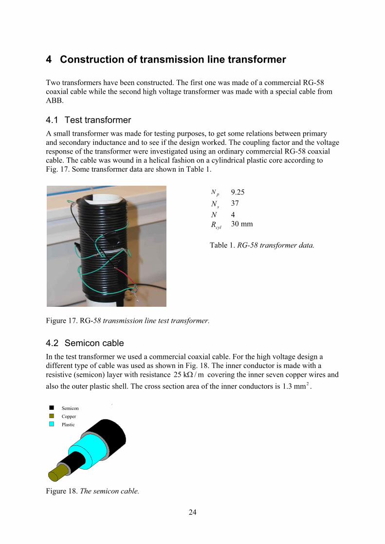
4.1 Test transformer A small transformer was made for testing purposes, to get some relations between primary and secondary inductance and to see if the design worked. The coupling factor and the voltage response of the transformer were investigated using an ordinary commercial RG-58 coaxial cable. The cable was wound in a helical fashion on a cylindrical plastic core according to Fig. 17. Some transformer data are shown in Table 1.
Figure 17. RG-58 transmission line test transformer.
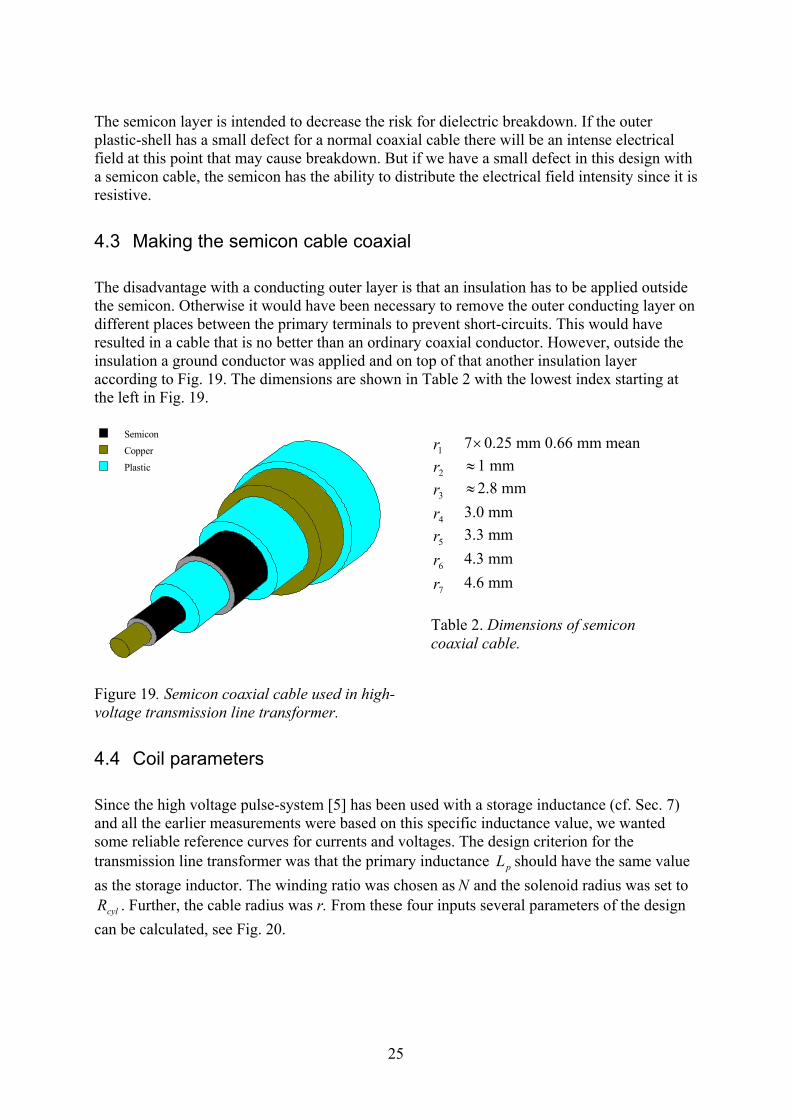
4.2 Semicon cable In the test transformer we used a commercial coaxial cable. For the high voltage design a different type of cable was used as shown in Fig. 18. The inner conductor is made with a resistive (semicon) layer with resistance m/k25 Ω covering the inner seven copper wires and also the outer plastic shell. The cross section area of the inner conductors is 2mm3.1 .
Semicon
Copper
Plastic
Figure 18. The semicon cable.
pN 9.25
sN 37 N 4
cylR 30 mm Table 1. RG-58 transformer data.
25
The semicon layer is intended to decrease the risk for dielectric breakdown. If the outer plastic-shell has a small defect for a normal coaxial cable there will be an intense electrical field at this point that may cause breakdown. But if we have a small defect in this design with a semicon cable, the semicon has the ability to distribute the electrical field intensity since it is resistive.
4.3 Making the semicon cable coaxial The disadvantage with a conducting outer layer is that an insulation has to be applied outside the semicon. Otherwise it would have been necessary to remove the outer conducting layer on different places between the primary terminals to prevent short-circuits. This would have resulted in a cable that is no better than an ordinary coaxial conductor. However, outside the insulation a ground conductor was applied and on top of that another insulation layer according to Fig. 19. The dimensions are shown in Table 2 with the lowest index starting at the left in Fig. 19.
Figure 19. Semicon coaxial cable used in high- voltage transmission line transformer.
4.4 Coil parameters Since the high voltage pulse-system [5] has been used with a storage inductance (cf. Sec. 7) and all the earlier measurements were based on this specific inductance value, we wanted some reliable reference curves for currents and voltages. The design criterion for the transmission line transformer was that the primary inductance pL should have the same value as the storage inductor. The winding ratio was chosen as N and the solenoid radius was set to
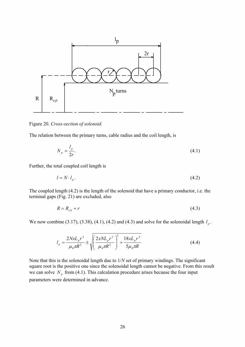
cylR . Further, the cable radius was r. From these four inputs several parameters of the design can be calculated, see Fig. 20.
1r 7×0.25 mm 0.66 mm mean
2r ≈ 1 mm
3r ≈ 2.8 mm
4r 3.0 mm
5r 3.3 mm
6r 4.3 mm
7r 4.6 mm Table 2. Dimensions of semicon coaxial cable.
Semicon
Copper
Plastic
26
R
r
2r
cyl
l
RN turnsp
p
Figure 20. Cross-section of solenoid. The relation between the primary turns, cable radius and the coil length, is
.2rl
N pp = (4.1)
Further, the total coupled coil length is
.plNl ⋅= (4.2) The coupled length (4.2) is the length of the solenoid that have a primary conductor, i.e. the terminal gaps (Fig. 21) are excluded, also
rRR cyl += (4.3) We now combine (3.17), (3.38), (4.1), (4.2) and (4.3) and solve for the solenoidal length pl .
RrxL
RrxNL
RrNxL
l pppp πµπµπµ 0
22
20
2
20
2
51822
+
±= (4.4)
Note that this is the solenoidal length due to 1/N set of primary windings. The significant square root is the positive one since the solenoidal length cannot be negative. From this result we can solve pN from (4.1). This calculation procedure arises because the four input parameters were determined in advance.
27
4.5 Helical geometry The helix [11] can be described in parametric form as
θθπθθπθθ
rzRyRx
2)()2sin()()2cos()(
===
pN≤≤ θ0 (4.5)
where the parameters R and r are defined as in Fig. 20. Further, differentiation of (4.5) gives
θθθπθπθθπθπθ
rddzdRdydRdx
2)()2cos(2)()2sin(2)(
==
−= (4.6)
Then an integration is performed to get the helical primary cable length ,Hpl
.2)()()( 222
0
222p
Np
Hp NRrddzdydxl ⋅+=++= ∫ πθθθθ (4.7)
Note that this is the cable length of one primary winding set, i.e. a total of N. All this can be done with Matlab, the m-file is found on the enclosed CD. Now a small correction according to Fig. 21 needs to be done when the secondary cable length is calculated.
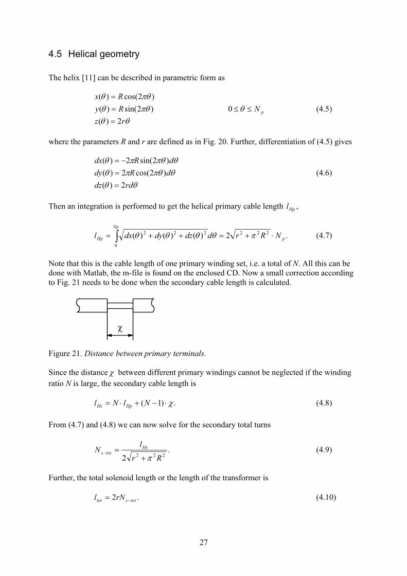
Figure 21. Distance between primary terminals. Since the distance χ between different primary windings cannot be neglected if the winding ratio N is large, the secondary cable length is
.)1( χ⋅−+⋅= NlNl HpHs (4.8) From (4.7) and (4.8) we can now solve for the secondary total turns
.2 222 Rr
lN Hs
totsπ+
=− (4.9)
Further, the total solenoid length or the length of the transformer is
.2 totstot rNl −= (4.10)
χ
28
The distance χ results in a new winding ratio, where the uncoupled secondary filaments are taken into account, though the coupled winding ratio, i.e. the ratio with surrounding primary conductor N (Eq. (3.1)) still holds. Finally, a modification of (3.38) with (4.1) and (4.9) gives the following secondary inductance where χ is taken into account:
.2
pp
totss L
NN
xL ⋅
⋅= − (4.11)
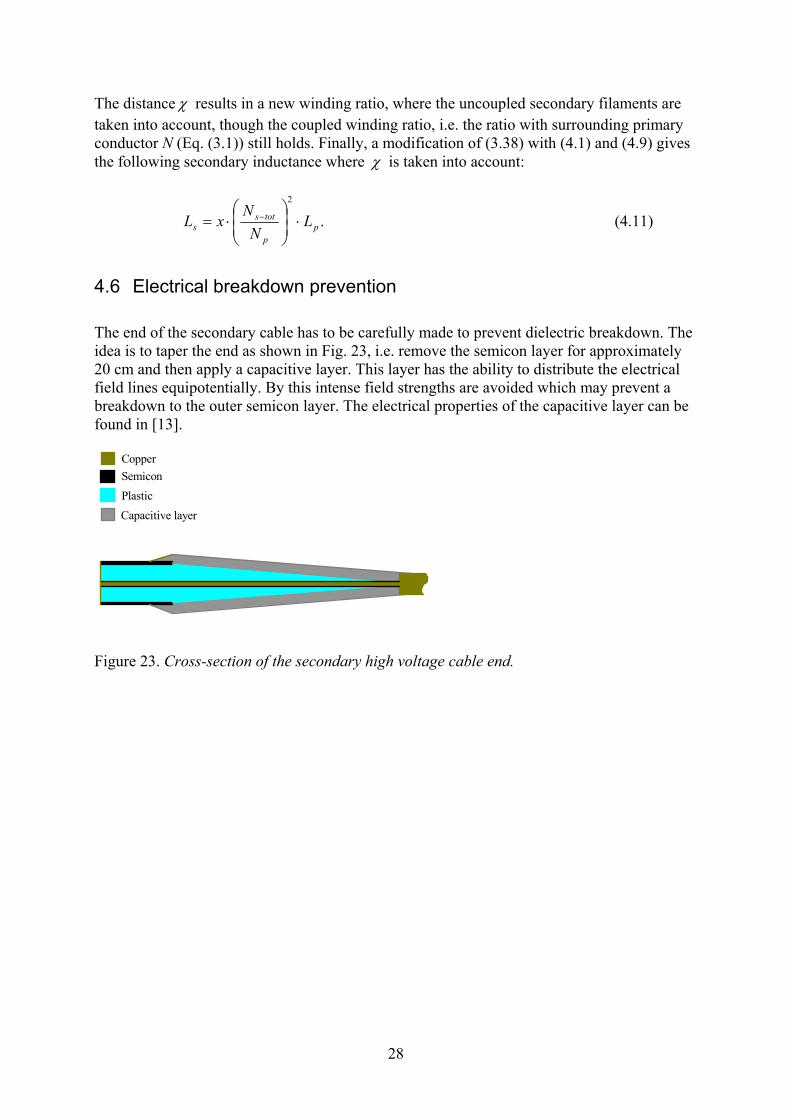
4.6 Electrical breakdown prevention The end of the secondary cable has to be carefully made to prevent dielectric breakdown. The idea is to taper the end as shown in Fig. 23, i.e. remove the semicon layer for approximately 20 cm and then apply a capacitive layer. This layer has the ability to distribute the electrical field lines equipotentially. By this intense field strengths are avoided which may prevent a breakdown to the outer semicon layer. The electrical properties of the capacitive layer can be found in [13].
Figure 23. Cross-section of the secondary high voltage cable end.
Copper
PlasticCapacitive layer
Semicon
29
5 Measurements
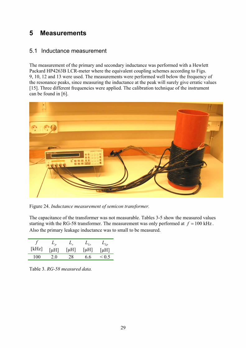
5.1 Inductance measurement The measurement of the primary and secondary inductance was performed with a Hewlett Packard HP4263B LCR-meter where the equivalent coupling schemes according to Figs. 9, 10, 12 and 13 were used. The measurements were performed well below the frequency of the resonance peaks, since measuring the inductance at the peak will surely give erratic values [15]. Three different frequencies were applied. The calibration technique of the instrument can be found in [6].
Figure 24. Inductance measurement of semicon transformer. The capacitance of the transformer was not measurable. Tables 3-5 show the measured values starting with the RG-58 transformer. The measurement was only performed at kHz100=f . Also the primary leakage inductance was to small to be measured.
f ]kHz[
pL ]µH[
sL ]µH[
LsL ]µH[
LpL ]µH[
100 2.0 28 6.6 < 0.5 Table 3. RG-58 measured data.
30
f
]kHz[ pL ]µH[
LpL ]µH[
pQ pR ]m[ Ω
pX ]m[ Ω
pZ ]m[ Ω
pθ ][°
1 4.34 2.43 3.6 7.5 28 29 75 10 4.0 1.24 27.3 9.25 250 251 88 100 3.7 1.0 61 40 2350 2350 89
Table 4. Primary semicon transformer data.
f ]kHz[
sL ]µH[
LsL ]µH[
sQ sR ]m[ Ω
sX ]m[ Ω
sZ ]m[ Ω
sθ ][°
1 54.8 13.8 1.4 241 344 420 55 10 53.7 12.6 11.8 287 3375 3387 85 100 52.4 12.0 46 710 32900 32910 89
Table 5. Secondary semicon transformer data. The different quantities are calculated directly by the instrument. Note that all values are inductively measured. The parameters are calculated as
fπω 2= (5.1)
n
n
RL
Qω
= (5.2)
nLX ω= (5.3) 22nnn XRZ += (5.4)
.arctan
=
n
nn R
Xθ (5.5)
If we use (3.21) to calculate the coupling factor from the measured leakage inductance, we get the results shown in Tables 6 and 7.
f ]kHz[
sk
100 0.874 Table 6. Secondary coupling coefficient for the RG-58 transformer.
f ]kHz[
pk
sk
1 0.663 0.865 10 0.830 0.875 100 0.852 0.878
Table 7. Semicon transformer coupling-coefficients for different frequencies.
31
As shown in Table 7 the coupling factors pk and sk are almost equal for kHz100=f . Since the transformer will be used with even higher frequency the following approximation can be done
.sp kkk ≈≈ The mutual inductance at 100 kHz according to (3.16) was calculated using the mean value of k from Table 7 as
.µH124.527.3865.0 ≈⋅⋅=M
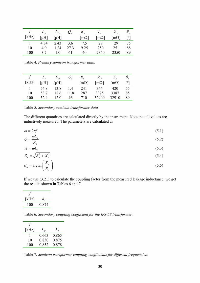
5.2 Measured compared to calculated inductance From the RG-58 transformer the relation between primary pxL and secondary inductance
sxL was estimated to
87
≈x (5.6)
This value is based on the measurement in Tab. 3 as illustrated in Fig. 22. Equations (3.35-3.37) are used to determine (5.6). In this relation the primary terminal distance χ is neglected, however relation (5.6) needs to be further investigated to determine its frequency dependence.
Figure 22. Relation between primary and secondary inductance for the RG-58 model.
32
If equation (4.11) and relation (5.6) are applied, the calculated values becomes as in Table 8. Quantity Calculated Measured Secondary inductance sL µH3.28 µH28 Table 8. Calculated vs measured values for RG-58 transformer. Since these equations seem to work well for estimation of the inductance, relation (5.6) was transferred to the semicon transformer giving the calculated values according to Table 9. Quantity Name Calculated Measured Primary windings pN 5.737 Secondary total windings (incl. uncoupled) totsN − 23.118 23 Winding relationship (Ns/Np).(input) N 4.000 Solenoid length totl 0.213 m 0.22 m Total length inner conductor (incl. uncoupled) Hsl 12.290 m Helical length per primary winding set Hpl 3.050 m Cable capacitance C 1.9922 nF Primary resistance pR 8.8 mΩ 40 mΩ Secondary resistance sR 154 mΩ 700 mΩ Secondary inductance (incl. uncoupled) sL 52.284 µH 52.4 µH Primary inductance (input) pL 3.7 µH 3.7 µH Table 9. Calculated vs. measured values for semicon transformer. As seen, the calculated inductances are quite accurate so the relations from the test transformer seem to perform well when translated to the semicon transformer. The transformer was made with the cable lengths given in Table 9. The calculated resistance values are too low, probably since the skin effect was not considered. For a more detailed discussion of the skin effect see Holmberg [4].
5.3 Transformer analysis set-up The RG-58 transformer was tested with two different coupling schemes, the first was done with a µF15.0 capacitor that was charged to approximately 1 kV. The energy was subsequently released into the primary winding with the use of a fast triggering tyristor. The second test was done with a DC-current device and the use of a switching field-effect transistor, for which schematics can be found in appendix A and on the CD. The HV transformer with semicon cable was tested with a µF1 capacitor, though it was also charged to approximately 1 kV. The analysis of the primary and secondary voltage was done with the aid of Matlab and its System Identification toolbox [10]. The equivalent circuits are designed with the electronic simulator program called P-spice [9]. When adding a lot of different capacitors and stray inductances the circuits becomes complex and difficult to analyse manually, making Pspice an excellent and fast tool.
33
5.4 Transfer function analysis The voltages at the primary and secondary terminals of both transformers were measured with LeCroy oscilloscopes (Fig. 25). These instruments have the ability to record the signals and save them on a portable disk.
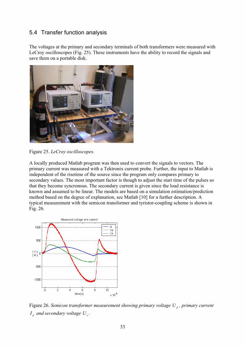
Figure 25. LeCroy oscilloscopes. A locally produced Matlab program was then used to convert the signals to vectors. The primary current was measured with a Tektronix current probe. Further, the input to Matlab is independent of the risetime of the source since the program only compares primary to secondary values. The most important factor is though to adjust the start time of the pulses so that they become syncronous. The secondary current is given since the load resistance is known and assumed to be linear. The models are based on a simulation estimation/prediction method based on the degree of explanation, see Matlab [10] for a further description. A typical measurement with the semicon transformer and tyristor-coupling scheme is shown in Fig. 26.
Figure 26. Semicon transformer measurement showing primary voltage pU , primary current
pI and secondary voltage sU .
34
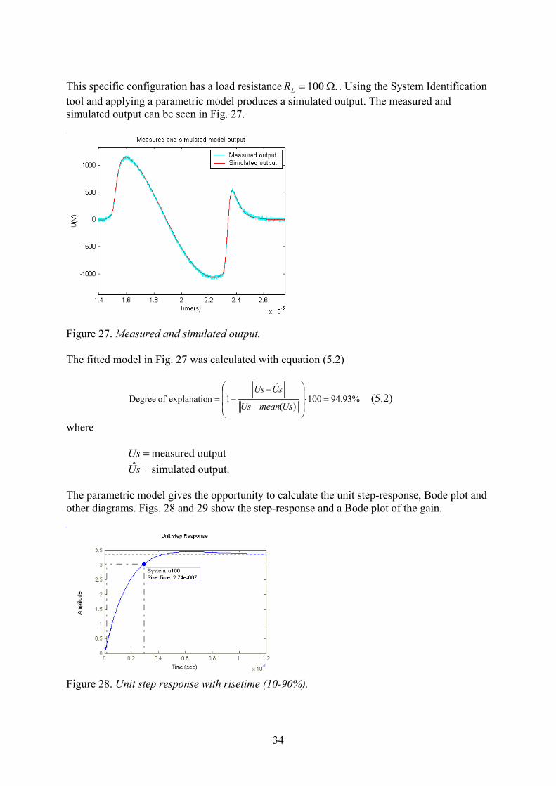
This specific configuration has a load resistance .100 Ω=LR . Using the System Identification tool and applying a parametric model produces a simulated output. The measured and simulated output can be seen in Fig. 27.
Figure 27. Measured and simulated output. The fitted model in Fig. 27 was calculated with equation (5.2)
%93.94100)(
ˆ1nexplanatio ofDegree =⋅
−
−−=
UsmeanUs
sUUs (5.2)
where
=Us measured output =sU simulated output.
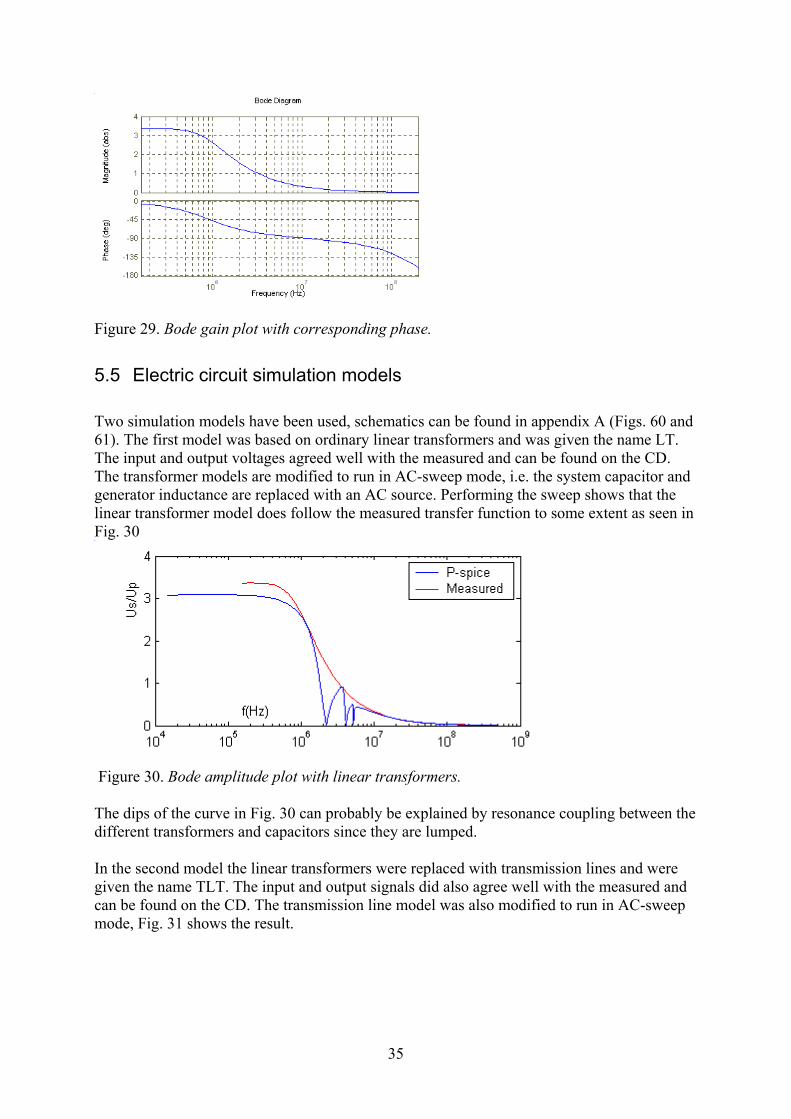
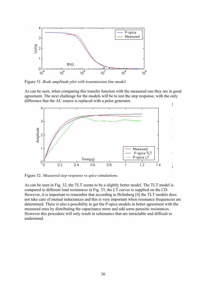
The parametric model gives the opportunity to calculate the unit step-response, Bode plot and other diagrams. Figs. 28 and 29 show the step-response and a Bode plot of the gain.
Figure 28. Unit step response with risetime (10-90%).
35
Figure 29. Bode gain plot with corresponding phase.
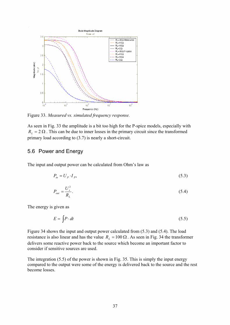
5.5 Electric circuit simulation models Two simulation models have been used, schematics can be found in appendix A (Figs. 60 and 61). The first model was based on ordinary linear transformers and was given the name LT. The input and output voltages agreed well with the measured and can be found on the CD. The transformer models are modified to run in AC-sweep mode, i.e. the system capacitor and generator inductance are replaced with an AC source. Performing the sweep shows that the linear transformer model does follow the measured transfer function to some extent as seen in Fig. 30
Figure 30. Bode amplitude plot with linear transformers. The dips of the curve in Fig. 30 can probably be explained by resonance coupling between the different transformers and capacitors since they are lumped. In the second model the linear transformers were replaced with transmission lines and were given the name TLT. The input and output signals did also agree well with the measured and can be found on the CD. The transmission line model was also modified to run in AC-sweep mode, Fig. 31 shows the result.
36
Figure 31. Bode amplitude plot with transmission line model. As can be seen, when comparing this transfer function with the measured one they are in good agreement. The next challenge for the models will be to test the step response, with the only difference that the AC source is replaced with a pulse generator.
Figure 32. Measured step response vs spice simulations. As can be seen in Fig. 32, the TLT seems to be a slightly better model. The TLT model is compared to different load resistances in Fig. 33, the LT curves is supplied on the CD. However, it is important to remember that according to Holmberg [4] the TLT models does not take care of mutual inductances and this is very important when resonance frequencies are determined. There is also a possibility to get the P-spice models in better agreement with the measured ones by distributing the capacitance more and add some parasitic resistances. However this procedure will only result in schematics that are intractable and difficult to understand.
37
Figure 33. Measured vs. simulated frequency response. As seen in Fig. 33 the amplitude is a bit too high for the P-spice models, especially with
Ω= 2LR . This can be due to inner losses in the primary circuit since the transformed primary load according to (3.7) is nearly a short-circuit.
5.6 Power and Energy The input and output power can be calculated from Ohm’s law as
,PPin IUP ⋅= (5.3)
.2
L
sout R
UP = (5.4)
The energy is given as
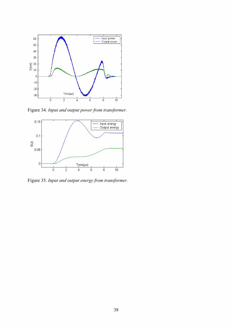
∫ ⋅= dtPE (5.5) Figure 34 shows the input and output power calculated from (5.3) and (5.4). The load resistance is also linear and has the value Ω= 100LR . As seen in Fig. 34 the transformer delivers some reactive power back to the source which become an important factor to consider if sensitive sources are used. The integration (5.5) of the power is shown in Fig. 35. This is simply the input energy compared to the output were some of the energy is delivered back to the source and the rest become losses.
38
Figure 34. Input and output power from transformer.
Figure 35. Input and output energy from transformer.
39
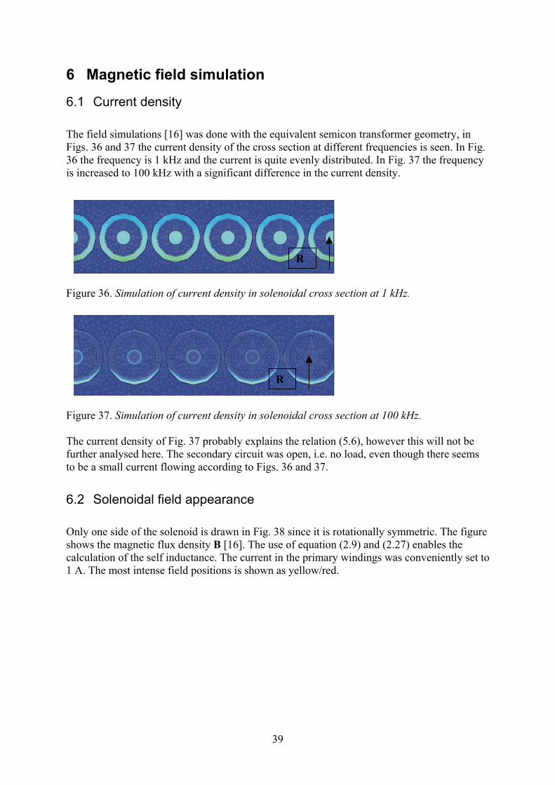
6 Magnetic field simulation 6.1 Current density The field simulations [16] was done with the equivalent semicon transformer geometry, in Figs. 36 and 37 the current density of the cross section at different frequencies is seen. In Fig. 36 the frequency is 1 kHz and the current is quite evenly distributed. In Fig. 37 the frequency is increased to 100 kHz with a significant difference in the current density.
Figure 36. Simulation of current density in solenoidal cross section at 1 kHz.
Figure 37. Simulation of current density in solenoidal cross section at 100 kHz. The current density of Fig. 37 probably explains the relation (5.6), however this will not be further analysed here. The secondary circuit was open, i.e. no load, even though there seems to be a small current flowing according to Figs. 36 and 37.
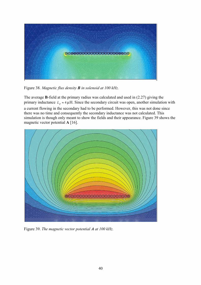
6.2 Solenoidal field appearance Only one side of the solenoid is drawn in Fig. 38 since it is rotationally symmetric. The figure shows the magnetic flux density B [16]. The use of equation (2.9) and (2.27) enables the calculation of the self inductance. The current in the primary windings was conveniently set to 1 A. The most intense field positions is shown as yellow/red.
R
R
40
Figure 38. Magnetic flux density B in solenoid at 100 kHz. The average B-field at the primary radius was calculated and used in (2.27) giving the primary inductance 4≈pL µH. Since the secondary circuit was open, another simulation with a current flowing in the secondary had to be performed. However, this was not done since there was no time and consequently the secondary inductance was not calculated. This simulation is though only meant to show the fields and their appearance. Figure 39 shows the magnetic vector potential A [16].
Figure 39. The magnetic vector potential A at 100 kHz.
41
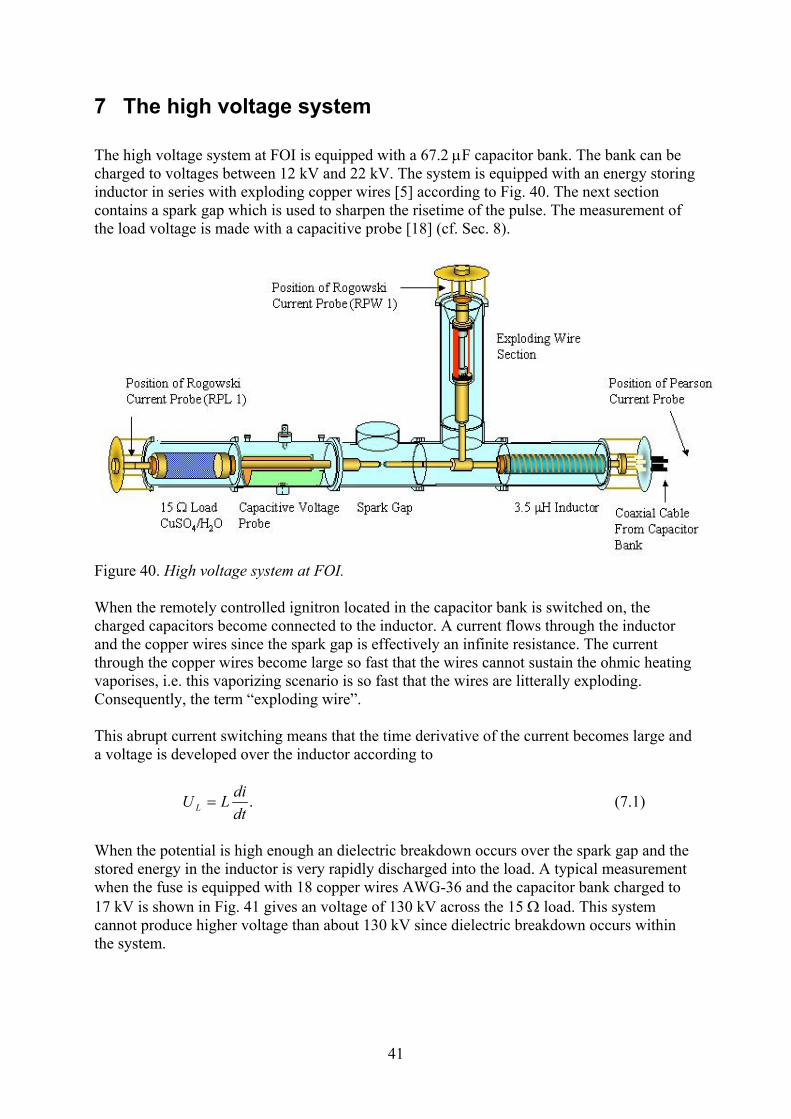
7 The high voltage system The high voltage system at FOI is equipped with a 67.2 µF capacitor bank. The bank can be charged to voltages between 12 kV and 22 kV. The system is equipped with an energy storing inductor in series with exploding copper wires [5] according to Fig. 40. The next section contains a spark gap which is used to sharpen the risetime of the pulse. The measurement of the load voltage is made with a capacitive probe [18] (cf. Sec. 8).
Figure 40. High voltage system at FOI. When the remotely controlled ignitron located in the capacitor bank is switched on, the charged capacitors become connected to the inductor. A current flows through the inductor and the copper wires since the spark gap is effectively an infinite resistance. The current through the copper wires become large so fast that the wires cannot sustain the ohmic heating vaporises, i.e. this vaporizing scenario is so fast that the wires are litterally exploding. Consequently, the term “exploding wire”. This abrupt current switching means that the time derivative of the current becomes large and a voltage is developed over the inductor according to
.dtdiLU L = (7.1)
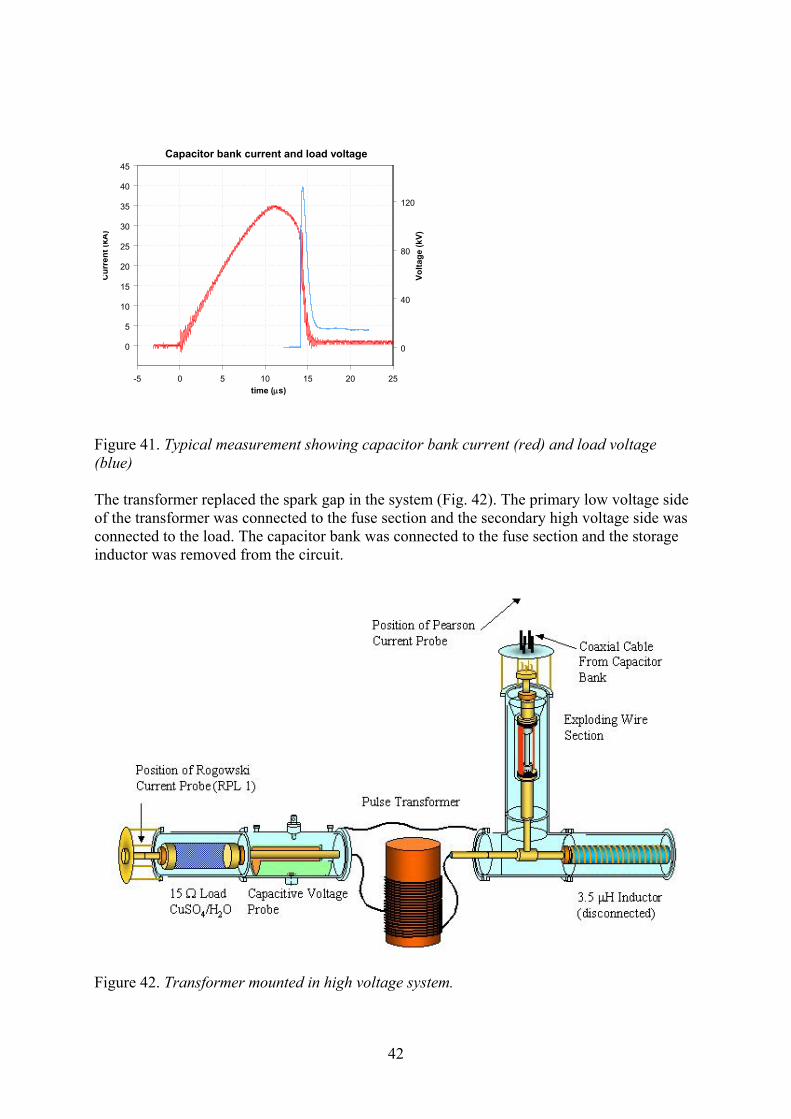
When the potential is high enough an dielectric breakdown occurs over the spark gap and the stored energy in the inductor is very rapidly discharged into the load. A typical measurement when the fuse is equipped with 18 copper wires AWG-36 and the capacitor bank charged to 17 kV is shown in Fig. 41 gives an voltage of 130 kV across the 15 Ω load. This system cannot produce higher voltage than about 130 kV since dielectric breakdown occurs within the system.
42
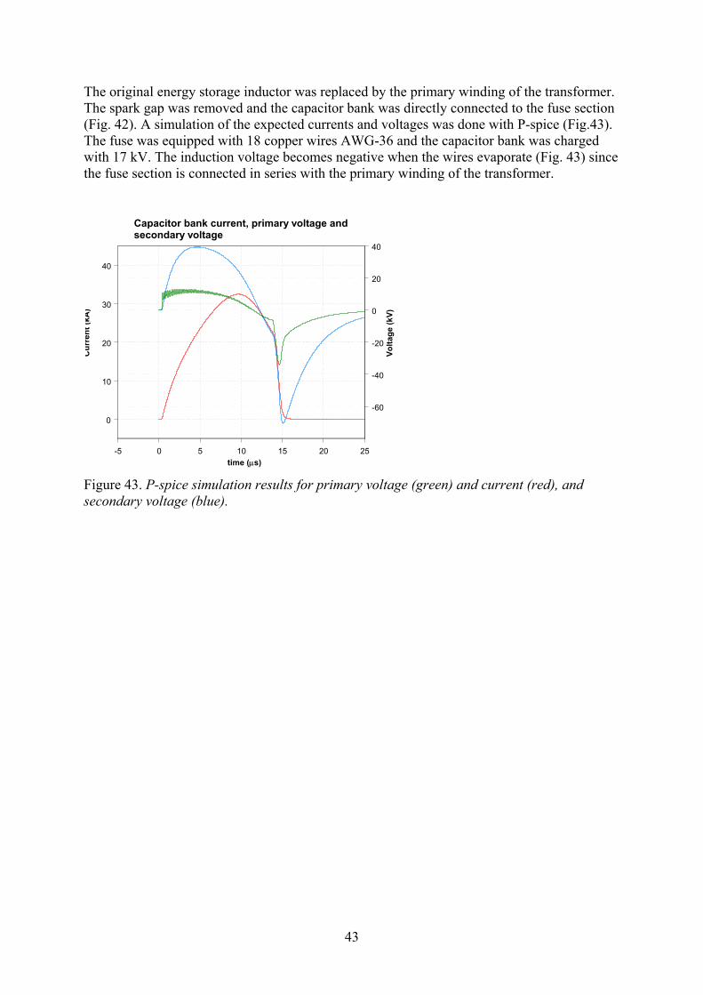
Figure 41. Typical measurement showing capacitor bank current (red) and load voltage (blue) The transformer replaced the spark gap in the system (Fig. 42). The primary low voltage side of the transformer was connected to the fuse section and the secondary high voltage side was connected to the load. The capacitor bank was connected to the fuse section and the storage inductor was removed from the circuit.
Figure 42. Transformer mounted in high voltage system.
-5 0 5 10 15 20 25time (µs)
0
5
10
15
20
25
30
35
40
45
Cur
rent
(kA
)
Capacitor bank current and load voltage
0
40
80
120
Volta
ge (k
V)
43
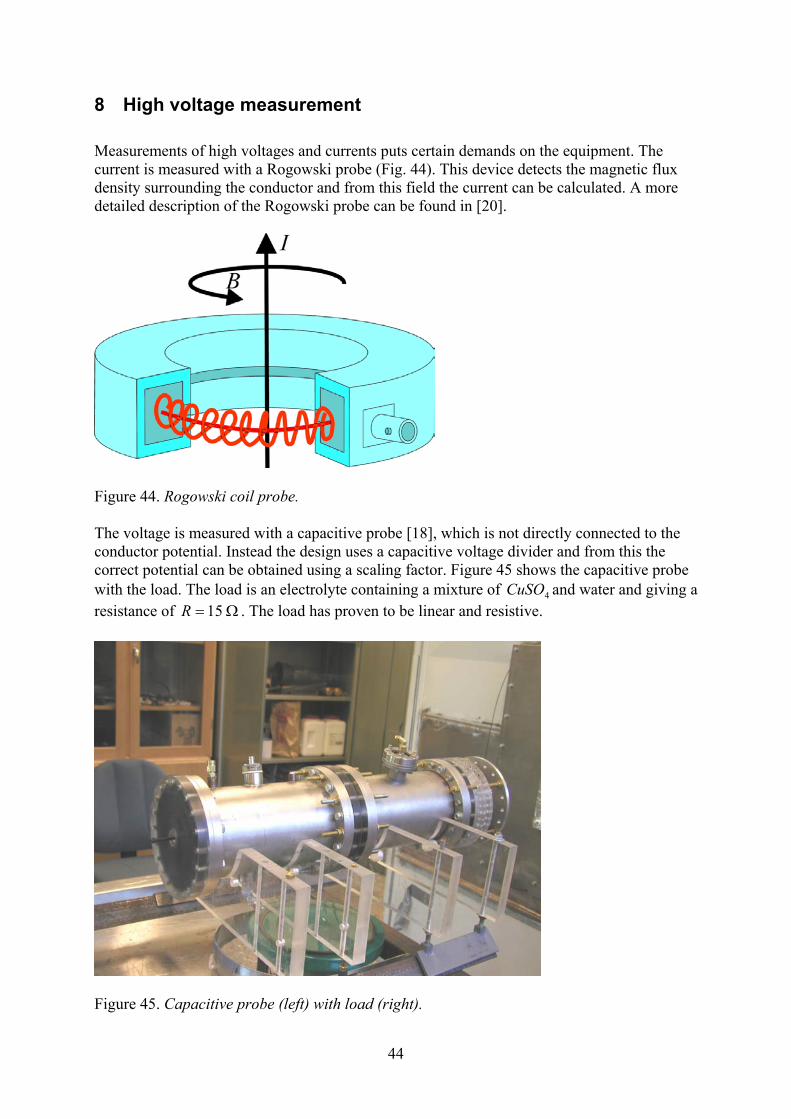
The original energy storage inductor was replaced by the primary winding of the transformer. The spark gap was removed and the capacitor bank was directly connected to the fuse section (Fig. 42). A simulation of the expected currents and voltages was done with P-spice (Fig.43). The fuse was equipped with 18 copper wires AWG-36 and the capacitor bank was charged with 17 kV. The induction voltage becomes negative when the wires evaporate (Fig. 43) since the fuse section is connected in series with the primary winding of the transformer.
Figure 43. P-spice simulation results for primary voltage (green) and current (red), and secondary voltage (blue).
-5 0 5 10 15 20 25time (µs)
0
10
20
30
40
Cur
rent
(kA
)
Capacitor bank current, primary voltage andsecondary voltage
-60
-40
-20
0
20
40
Volta
ge (k
V)
44
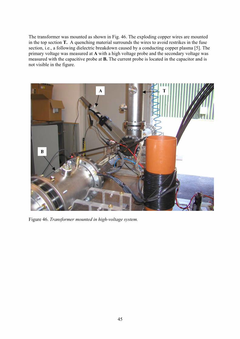
8 High voltage measurement Measurements of high voltages and currents puts certain demands on the equipment. The current is measured with a Rogowski probe (Fig. 44). This device detects the magnetic flux density surrounding the conductor and from this field the current can be calculated. A more detailed description of the Rogowski probe can be found in [20].
Figure 44. Rogowski coil probe. The voltage is measured with a capacitive probe [18], which is not directly connected to the conductor potential. Instead the design uses a capacitive voltage divider and from this the correct potential can be obtained using a scaling factor. Figure 45 shows the capacitive probe with the load. The load is an electrolyte containing a mixture of 4CuSO and water and giving a resistance of Ω= 15R . The load has proven to be linear and resistive.
Figure 45. Capacitive probe (left) with load (right).
45
The transformer was mounted as shown in Fig. 46. The exploding copper wires are mounted in the top section T. A quenching material surrounds the wires to avoid restrikes in the fuse section, i.e., a following dielectric breakdown caused by a conducting copper plasma [5]. The primary voltage was measured at A with a high voltage probe and the secondary voltage was measured with the capacitive probe at B. The current probe is located in the capacitor and is not visible in the figure.
Figure 46. Transformer mounted in high-voltage system.
A
B
T
46
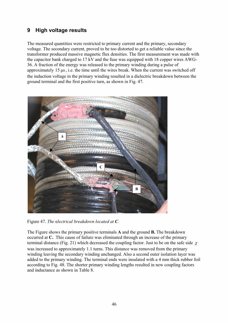
9 High voltage results The measured quantities were restricted to primary current and the primary, secondary voltage. The secondary current, proved to be too distorted to get a reliable value since the transformer produced massive magnetic flux densities. The first measurement was made with the capacitor bank charged to 17 kV and the fuse was equipped with 18 copper wires AWG-36. A fraction of the energy was released to the primary winding during a pulse of approximately µs15 , i.e. the time until the wires break. When the current was switched off the induction voltage in the primary winding resulted in a dielectric breakdown between the ground terminal and the first positive turn, as shown in Fig. 47.
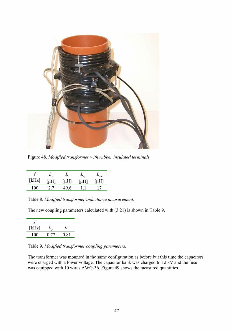
Figure 47. The electrical breakdown located at C. The Figure shows the primary positive terminals A and the ground B. The breakdown occurred at C. This cause of failure was eliminated through an increase of the primary terminal distance (Fig. 21) which decreased the coupling factor. Just to be on the safe side χ was increased to approximately 1.1 turns. This distance was removed from the primary winding leaving the secondary winding unchanged. Also a second outer isolation layer was added to the primary winding. The terminal ends were insulated with a 4 mm thick rubber foil according to Fig. 48. The shorter primary winding lengths resulted in new coupling factors and inductance as shown in Table 8.
C
A
B
47
Figure 48. Modified transformer with rubber insulated terminals.
f ]kHz[
pL ]µH[
sL ]µH[
LpL ]µH[
LsL ]µH[
100 2.7 49.6 1.1 17 Table 8. Modified transformer inductance measurement. The new coupling parameters calculated with (3.21) is shown in Table 9.
f ]kHz[
pk
sk
100 0.77 0.81
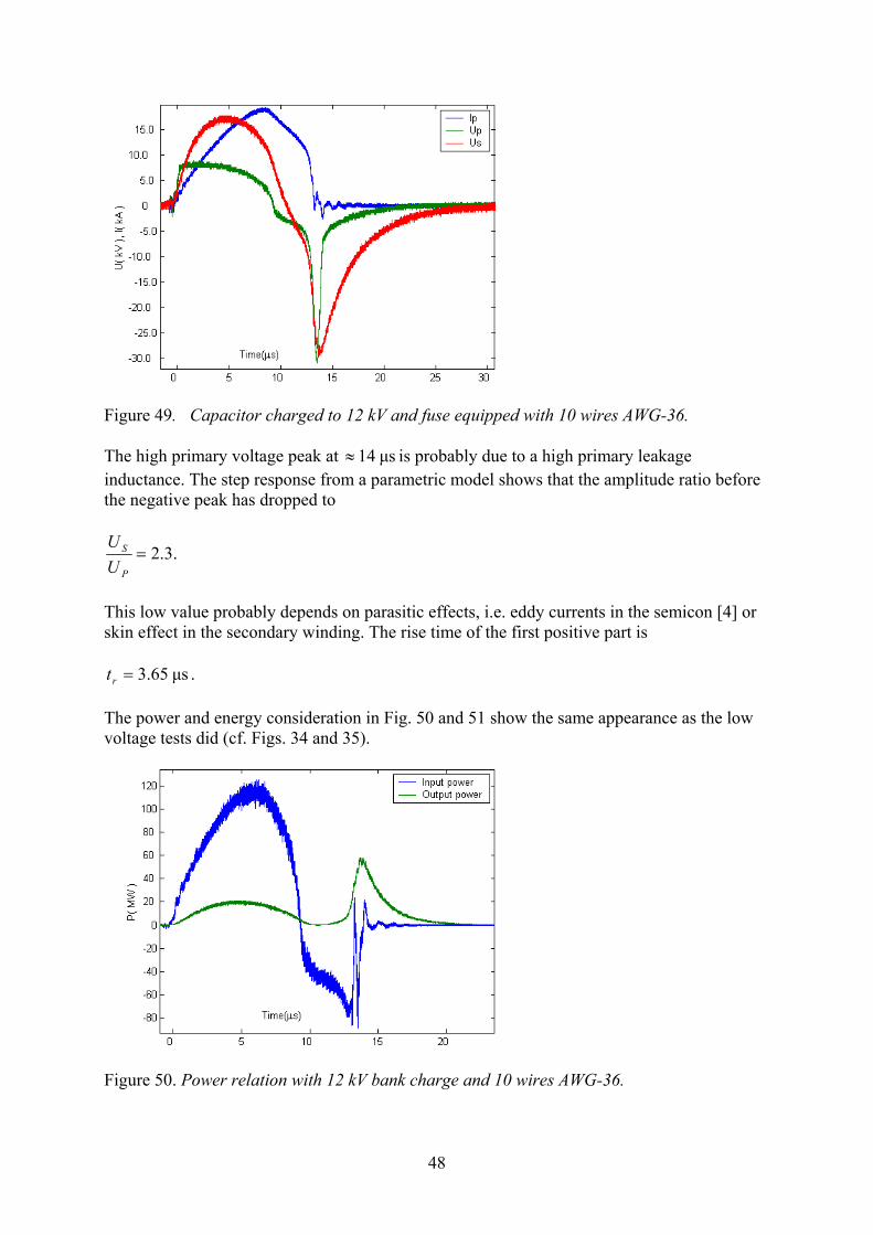
Table 9. Modified transformer coupling parameters. The transformer was mounted in the same configuration as before but this time the capacitors were charged with a lower voltage. The capacitor bank was charged to 12 kV and the fuse was equipped with 10 wires AWG-36. Figure 49 shows the measured quantities.
48
Figure 49. Capacitor charged to 12 kV and fuse equipped with 10 wires AWG-36. The high primary voltage peak at µs14≈ is probably due to a high primary leakage inductance. The step response from a parametric model shows that the amplitude ratio before the negative peak has dropped to
.3.2=P
S
UU
This low value probably depends on parasitic effects, i.e. eddy currents in the semicon [4] or skin effect in the secondary winding. The rise time of the first positive part is
µs65.3=rt . The power and energy consideration in Fig. 50 and 51 show the same appearance as the low voltage tests did (cf. Figs. 34 and 35).
Figure 50. Power relation with 12 kV bank charge and 10 wires AWG-36.
49
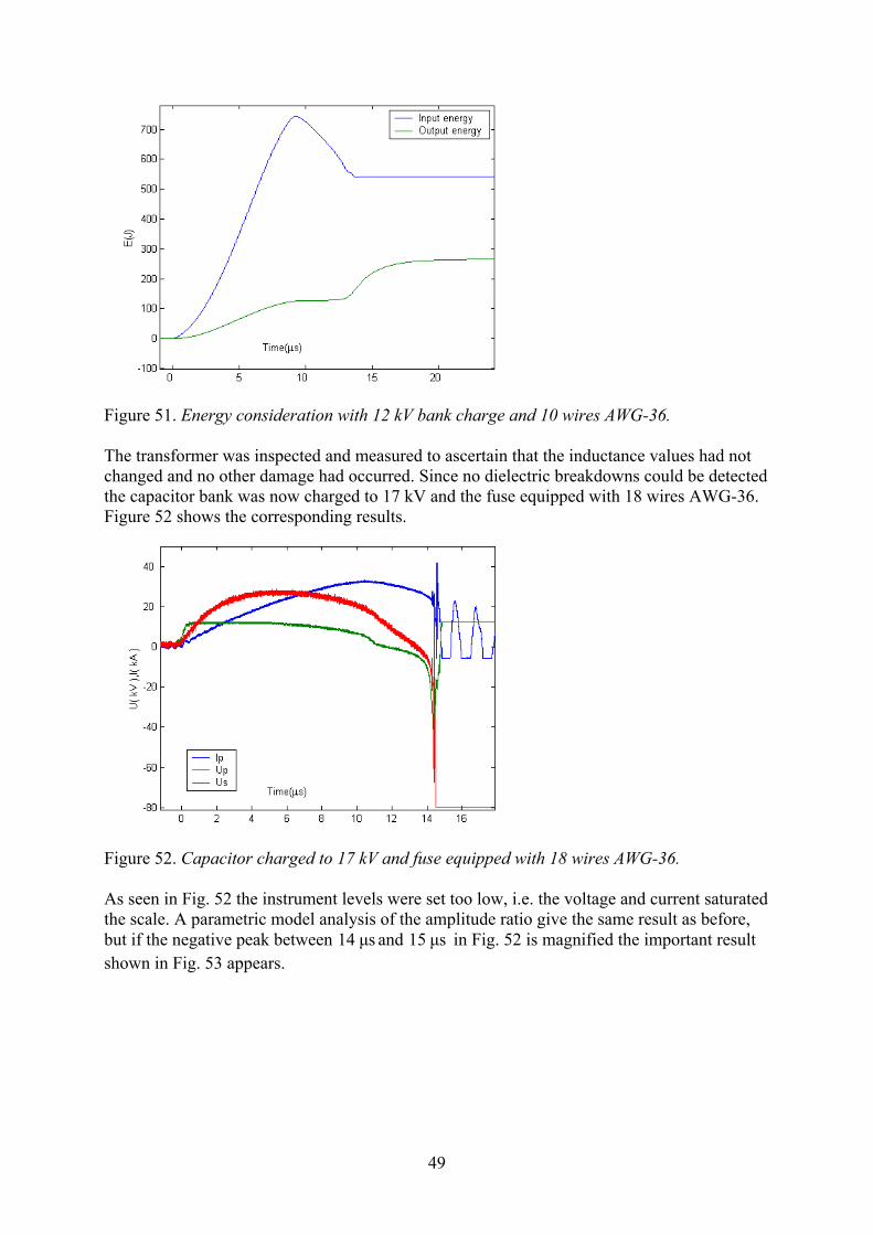
Figure 51. Energy consideration with 12 kV bank charge and 10 wires AWG-36. The transformer was inspected and measured to ascertain that the inductance values had not changed and no other damage had occurred. Since no dielectric breakdowns could be detected the capacitor bank was now charged to 17 kV and the fuse equipped with 18 wires AWG-36. Figure 52 shows the corresponding results.
Figure 52. Capacitor charged to 17 kV and fuse equipped with 18 wires AWG-36. As seen in Fig. 52 the instrument levels were set too low, i.e. the voltage and current saturated the scale. A parametric model analysis of the amplitude ratio give the same result as before, but if the negative peak between µs14 and µs15 in Fig. 52 is magnified the important result shown in Fig. 53 appears.
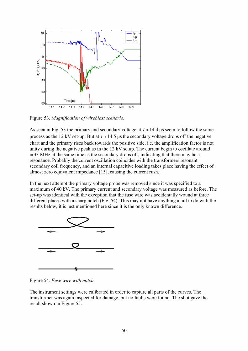
50
Figure 53. Magnification of wireblast scenario. As seen in Fig. 53 the primary and secondary voltage at µs4.14≈t seem to follow the same process as the 12 kV set-up. But at µs5.14≈t the secondary voltage drops off the negative chart and the primary rises back towards the positive side, i.e. the amplification factor is not unity during the negative peak as in the 12 kV setup. The current begin to oscillate around ≈ 33 MHz at the same time as the secondary drops off, indicating that there may be a resonance. Probably the current oscillation coincides with the transformers resonant secondary coil frequency, and an internal capacitive loading takes place having the effect of almost zero equivalent impedance [15], causing the current rush. In the next attempt the primary voltage probe was removed since it was specified to a maximum of 40 kV. The primary current and secondary voltage was measured as before. The set-up was identical with the exception that the fuse wire was accidentally wound at three different places with a sharp notch (Fig. 54). This may not have anything at all to do with the results below, it is just mentioned here since it is the only known difference.
Figure 54. Fuse wire with notch. The instrument settings were calibrated in order to capture all parts of the curves. The transformer was again inspected for damage, but no faults were found. The shot gave the result shown in Figure 55.
51
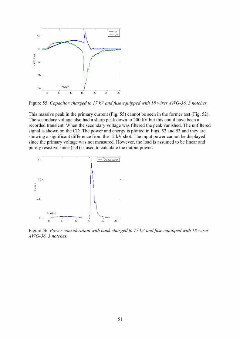
Figure 55. Capacitor charged to 17 kV and fuse equipped with 18 wires AWG-36, 3 notches. This massive peak in the primary current (Fig. 55) cannot be seen in the former test (Fig. 52). The secondary voltage also had a sharp peak down to 200 kV but this could have been a recorded transient. When the secondary voltage was filtered the peak vanished. The unfiltered signal is shown on the CD. The power and energy is plotted in Figs. 52 and 53 and they are showing a significant difference from the 12 kV shot. The input power cannot be displayed since the primary voltage was not measured. However, the load is assumed to be linear and purely resistive since (5.4) is used to calculate the output power.
Figure 56. Power consideration with bank charged to 17 kV and fuse equipped with 18 wires AWG-36, 3 notches.
52
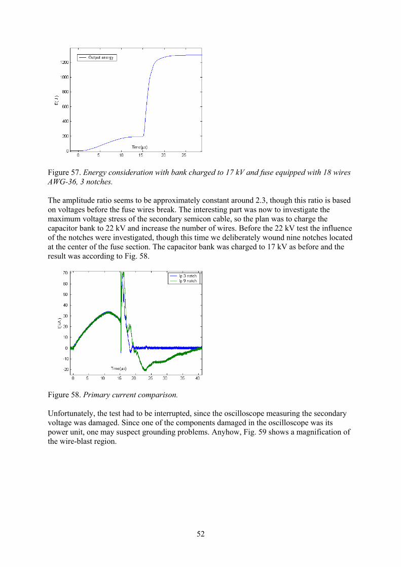
Figure 57. Energy consideration with bank charged to 17 kV and fuse equipped with 18 wires AWG-36, 3 notches. The amplitude ratio seems to be approximately constant around 2.3, though this ratio is based on voltages before the fuse wires break. The interesting part was now to investigate the maximum voltage stress of the secondary semicon cable, so the plan was to charge the capacitor bank to 22 kV and increase the number of wires. Before the 22 kV test the influence of the notches were investigated, though this time we deliberately wound nine notches located at the center of the fuse section. The capacitor bank was charged to 17 kV as before and the result was according to Fig. 58.
Figure 58. Primary current comparison. Unfortunately, the test had to be interrupted, since the oscilloscope measuring the secondary voltage was damaged. Since one of the components damaged in the oscilloscope was its power unit, one may suspect grounding problems. Anyhow, Fig. 59 shows a magnification of the wire-blast region.
53
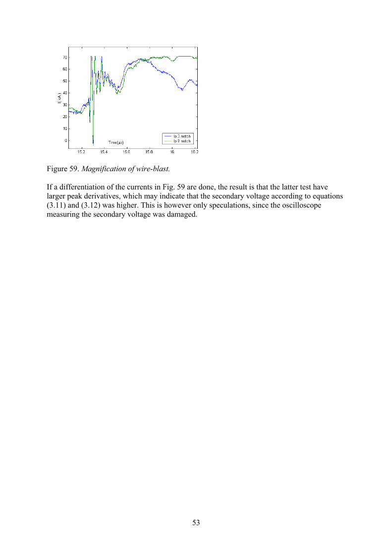
Figure 59. Magnification of wire-blast. If a differentiation of the currents in Fig. 59 are done, the result is that the latter test have larger peak derivatives, which may indicate that the secondary voltage according to equations (3.11) and (3.12) was higher. This is however only speculations, since the oscilloscope measuring the secondary voltage was damaged.
54
10 Conclusions 10.1 Summary Simulations during the low voltage tests show that the P-spice models perform well. The high voltage simulation is also very accurate for the positive slow peaks, even if the high voltage generation when the wires break cannot be achieved with P-spice simulations. This may indicate that the simulation models are not complete for resonance phenomena. The semicon cable has show very good high voltage characteristics, since it can cope with a voltage stress of 150 kV with an outer diameter of 6 mm without breakdown. In this test the pulse width is approximately µs2.1 during this output voltage.
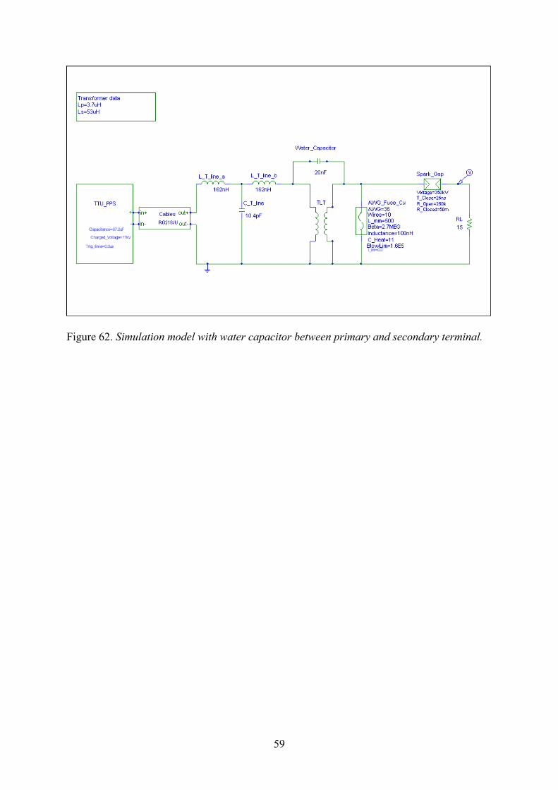
10.2 Suggestions for improvements A better terminal insulation should be applied so that the primary winding enclose as much as possible of the secondary cable, resulting in a better coupling factor. The solution may be to add a high performance insulation for a complete turn between the grounded and the first positive turn on each terminal. Experimental work is needed to investigate how the diameter of the solenoid influences the coupling factor. The design could be equipped with modern ferrite core to achieve better coupling. Another interesting simulation is made with the coupling scheme shown in appendix A Fig. 62. In this set-up the transformer was equipped with the exploding wires on the secondary side. The use of a capacitor between the primary and secondary terminal works as an efficient energy buffer. The capacitor is charged during the time of voltage build-up on the secondary. Then, as the spark gap strike, the transformer deliver its energy and on top of that the capacitor leaves its charged energy. The result is a very rapid pulse with high energy. The main problem with this design is the excessive force on the capacitor since the energy is delivered very fast. Therefore the use of a water capacitor made of some strong material may be an alternative. The capacitor can also be directly connected from the secondary terminal to ground giving an even faster pulse. However, this procedure has the effect of an increasing voltage stress in the capacitor [9], since it is connected directly to ground. In this model the values of the capacitance can vary between 10 nF and 30 nF. The water capacitor is described in [17]. Further tests of the twisted copper wires should be performed to see if there is any possibility to achieve higher time derivative of the current.
55
References [ 1 ] R.K.Wangsness, Electromagnetic Fields 2nd ed. John Wiley & Sons 1986 ISBN 0-471- 81186-6. [ 2 ] D.K.Cheng, Field and Wave electromagnetics 2nd ed. Addison Wesley 1989 ISBN 0-201-52820-7. [ 3 ] W.M.Flanagan, Handbook of transformer design and applications 2nd ed. Mc Graw Hill 1993 ISBN 0-07-021291. [ 4 ] P.Holmberg, Modelling the transient response of windings, laminated steel cores and electromagnetic power devices by means of lumped circuits. Acta Universitatis Upsaliensis Uppsala Universitet 2000 ISBN 91-554-4877-1. [ 5 ] P.Appelgren G.Bjarnholt T.Hultman T.Hurtig S.E.Nyholm, High voltage generation and power conditioning with TTHPM. December 2000 ISSN 1104-9154. [ 6 ] M.Seth, Inductance of an explosive generator. Diploma work. January 1998 ISSN 1104-9154. [ 7 ] V.G.Gaaze G.A.Schneerson, A high voltage cable transformer for producing strong pulsed currents. December 1965 UDC 621.314.228. [ 8 ] V.J.Spataro, Design high performance pulse transformers in easy stages. EDN access. March 1995 http://archives.e-insite.net/archives/ednmag/reg/1995/031695/06df3.htm . [ 9 ] P-spice, Circuit analysis program version 8.0. MicroSim corp. 20 Fairbanks,Irvine CA. [10] Matlab, The language of technical computing version 6.1.0.450 release 12.1. [11] L.Råde B.Westergren, Beta mathematics handbook 4th ed. Studentlitteratur 1998 ISBN 91-44-00839-2. [12] B.L.Freeman W.H.Bostick, Transformers for explosive pulsed power coupling to various loads. Los Alamos National Laboratory. [13] U.Lind, Egenskaper hos fältstyrande duk med kiselkarbid för kraftkabel avslutningar. Diploma work. 1993 Chalmers Tekniska Högskola. [14] Wheeler’s inductance formula. http://unitmath.com/um/p/Examples/PulsedPower/Inductance/Inductance.html [15] M.Behrend, Coupling between primary and secondary coils. March 24 2000. http://home.earthlink.net/~electronxlc/difmodel/coupling.html [16] ABB ACE Magnetic field simulation software.

56
[17] B.Bolund, High field properties of pulsed water capacitor. Uppsala Universitet 2002 ISSN 1401-5757. [18] P.Appelgren, Design and calibration of a capacitive voltage probe for use in the TTHPM system. FOI-R-0428. ISSN 1650-1942. [19] A.Homma, High-voltage subnanosecond pulse transformer composed of parallel-strip transmission lines. Review of scientific instruments January 1999. Volume 70, number 1. S0034-6748(99)03801-0 [20] S.E.Nyholm P.Appelgren T.Hurtig T.Hultman, Design and calculation of Rogowski current probes FOI-R-- 0427--SE
57
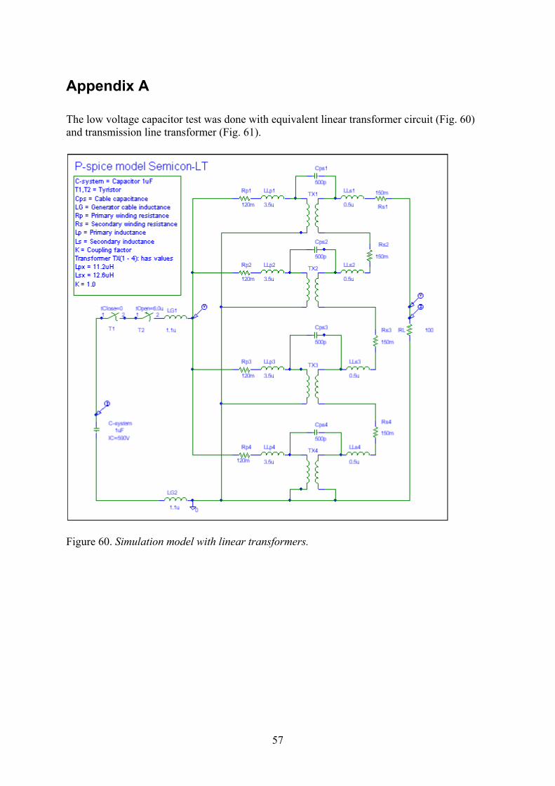
Appendix A The low voltage capacitor test was done with equivalent linear transformer circuit (Fig. 60) and transmission line transformer (Fig. 61).
Figure 60. Simulation model with linear transformers.
58
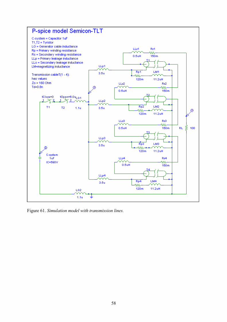
Figure 61. Simulation model with transmission lines.
59
Figure 62. Simulation model with water capacitor between primary and secondary terminal.


