Embed Size (px)
Citation preview
coatings
Article
Electrodeposition of ZnO/Cu2O Heterojunctions onNi-Mo-P Electroless Coating
Nelly Maria Rosas-Laverde 1, Alina Iuliana Pruna 2,3,* , Jesus Cembrero 3
and David Busquets-Mataix 3
1 Department of Materials, Escuela Politécnica Nacional, Quito 170524, Ecuador; [email protected] Center for Surface Science and Nanotechnology, Polytechnic University of Bucharest,
060042 Bucharest, Romania3 Institute of Materials Technology, Universitat Politècnica de València, 46022 Valencia, Spain;
[email protected] (J.C.); [email protected] (D.B.-M.)* Correspondence: [email protected]
Received: 25 August 2020; Accepted: 27 September 2020; Published: 29 September 2020
Abstract: Electroless Ni-Mo-P coatings were deposited onto ceramic tiles in order to be employedas electrodes for the electrodeposition of ZnO and Cu2O heterojunction layers. Varying conditions,such as duration, annealing of the electroless coating and applied potential, and duration for ZnOelectrodeposition were studied in order to optimize the properties of the ZnO/Cu2O heterojunctionstoward improved photoelectrical performance. The coatings were evaluated in terms of morphology,crystalline structure, and by electrochemical and photoelectrical means. The obtained results indicatedthat a prolonged annealing treatment at low temperature is beneficial to improve the roughnessand electrical conductivity of the Ni-Mo-P coating to further enhance the electrodeposition of ZnO.The morphology analysis revealed continuous and homogeneous Ni-Mo-P coatings. The formationof cube-like Cu2O crystals with larger grain size was induced by increasing the deposition durationof ZnO. The properties of ZnO layer are much improved when a higher cathodic potential is applied(−0.8 V) for 1 h, resulting in optimum photoelectric parameters as 1.44 mA·cm−2 for the JSC and760.23 µV for the VOC value, respectively, for the corresponding heterojunction solar cell.
Keywords: electroless coating; Ni-Mo-P; ceramic substrate; electrodeposition; ZnO; Cu2O
1. Introduction
Ceramic materials show excellent chemical stability, high hardness and wear resistance, and havehigher melting temperature in comparison to other materials [1,2]. Owing to these properties, ceramicmaterials are employed in various fields such as heat exchangers, motor parts, electrical and electroniccomponents, implants [1], as well as in electrical [3] and power electronic systems [4], as mechanicalsupports [5], and building-integrated photovoltaics (BIPV) [6].
The ceramics show an important drawback in some applications, namely they are poor conductorsof electricity and heat and they exhibit high fragility [2]. In this regard, surface modification bymethods including electroless deposition (ED) attracted attention in order to improve the electricalproperties of these non-conductive surfaces (polymer, ceramics) without using external current [7–10].The ED involves the following steps: (i) surface treatment, (ii) catalytic activation, (iii) electrolessprocess, and (iv) annealing treatment [11]. The deposition bath is formed by a metal salt, a complexingand reducing agent, a stabilizer, an inhibitor, and others (pH regulators, wetting and polishingagents) [11,12]. Factors such as temperature, time, pH, and chemical composition directly influencethe morphology, composition, and final structure of electroless coating, as well as the electrical andmagnetic properties [12–14]. For example, thickness and size grain dependence were observed with
Coatings 2020, 10, 935; doi:10.3390/coatings10100935 www.mdpi.com/journal/coatings
Coatings 2020, 10, 935 2 of 14
immersion duration of the substrate in the deposition bath [15]; pH has a direct relation with thereaction rate [14]; the activation process was shown to control the rate and mechanism of coatingdeposition [16], while substrate morphology affects the roughness, hydrophobicity, and thermalconductivity of the electroless coating [17]. The composition and annealing treatment were shown toaffect the continuity of the coatings [18].
On the other hand, the electrodeposition process (ELD) is an easy and cost-effective method tofabricate nanostructures of various materials including metal and semiconductor oxide with tailoredcomposition, thickness, and morphology by simply adjusting the electrochemical parameters [9,19].ELD process can be carried out at low temperature in atmospheric conditions and requires a simpleand cheap setup [20]. The ELD technique has showed high potential to be used in the nanophotonics,specifically in optoelectronic industry [9], photovoltaics, and superconductor applications as it allowsthe fabrication of large uniform areas of tailored films at low cost [21] and high crystallinity [22].
In the photovoltaics field, some amorphous silicon [23], CuInGaSe2 [24] or Cu2ZnSn(S,Se)4 [25]solar cells were reported as BIPV. The semiconductor heterojunction solar cells (SCs) attractedincreased interest because of the advantages such as high efficiency [26], easy fabrication, and lowcost [27]. Among the different heterojunction solar cells such as intrinsic thin-layer, silicon, CdTe/CdS,CIGS/CdS [28], it was indicated that the ZnO/Cu2O [29,30] ones show a great absorption in theUV-visible region [31], their components being non-toxic and earth-abundant [32]. Furthermore,the alignment of ZnO/Cu2O heterojunction allows the separation and transportation of electro-holepairs [33,34]. The ZnO/Cu2O heterojunction SCs can be fabricated by techniques including thermaloxidation, plasma evaporation, sputtering, chemical vapor deposition, pulsed laser deposition, andelectrodeposition [35–37]. The electrodeposition approach is easy, low cost, and scalable [35,36] whichmakes it highly appropriate.
The ZnO/Cu2O heterojunctions are usually fabricated onto glass substrates coated with transparentconductive oxides (TCOs) such as indium-doped tin oxide (ITO) [38–42] or fluorine-doped tin oxide(FTO) [43–45] playing the role of frontal contact [46]. Such TCOs are employed because of theirhigh transparency and conductivity that reduce the resistive losses [47]. These TCOs are used inthe amorphous silicon solar cells as they allow the improvement in the solar light management [48].Nevertheless, their high cost and chemical instability triggered researches toward reducing theiruse [48,49]. One of the alternatives to TCOs is an electroless coating which could also extend theapplication toward an insulating substrate such as a ceramic tile, polymers, or biomaterials [50,51].Among the electroless coatings, the Ni-Mo-P one was reported for the fabrication of varying devicessuch as supercapacitor electrode [52] and proton exchange membrane fuel cells [53]. It is thus,of great challenge to find cheap insulating supports while employing scalable and low cost electricalfunctionalization and deposition, respectively, for optoelectronic devices [54].
The novelty of this study relies on the use of a ceramic tile as substrate for the fabrication ofZnO/Cu2O heterojunction solar cells. To this end, the ceramic surface was subjected to electrolessdeposition of a Ni-Mo-P coating to be further employed as electrode for the synthesis of the ZnOand Cu2O films by electrochemical deposition. The Ni-Mo-P coating was selected because of itseasy fabrication and good electrical properties. It is known that electrodeposited material propertiesare directly dependent on the substrate properties. Therefore, in order to understand the effects ofelectroless plating on the fabrication and performance of electrodeposited heterojunctions, the electrolessdeposition duration and heat treatment in vacuum conditions on the Ni-Mo-P properties are studiedalong with the electrodeposition parameters such as potential and duration in order to tailor theproperties of the heterojunction toward improved performance in photovoltaics.
Coatings 2020, 10, 935 3 of 14
2. Materials and Methods
2.1. Materials and Reagents
All chemicals were reagent grade and were used as received (Panreac, Barcelona, Spain). Palladiumcatalyst was prepared as reported elsewhere [8]. Ceramic substrate was fabricated from commercialpowder (Euroatomizado, Valencia, Spain) as reported elsewhere [8].
2.2. Electroless Plating of the Ceramic Surface
First, the ceramic surface was activated with palladium catalyst at 300 C for 12 h [8]. Then, theelectroless plating of Ni-Mo-P film was performed at 80 C and 300 rpm stirring rate from a bathcomposed of: NiSO4, Na2MoO4, NaH2PO2, C6H12O7, and Na2C4H4O6 in concentration (g L−1) of 7,3.9, 10.0, 15.0, and 10, respectively. NH4OH was used to adjust the pH to 10. The metallized ceramicwas further rinsed with water and air-dried. The plating time was varied from 30 to 300 min whilethe annealing treatment in vacuum conditions ranged from 160 C for 16 h to 400 C for 1 h (themetallized ceramic substrates were denoted as CSx-y where x is the plating time and y is the appliedheat treatment). These substrates were used to fabricate the p–n heterojunctions solar cells.
2.3. Electrodeposition of ZnO on Ni-Mo-P/Ceramic Substrate
In order to fabricate the p–n heterojunction SCs using metallized ceramic substrates,electrodeposition (ELD) technique was selected. ZnO was electrodeposited onto Ni-Mo-P-coatedceramic substrates from 5 mM ZnCl2 and 0.1 M KCl [29] in a deposition potential ranging from −0.6 to−0.8 V for 30 and 60 min at 75 C in order to analyze the growth of ZnO layer and its effect on theperformance of heterojunction SC using different substrates. In order to reference the electrodepositionof ZnO to the literature, a different batch of ceramic electrodes were obtained by coating the ceramicwith an ITO layer with an electrical conductivity of about 1.8 µΩ cm and thickness of 300 nm.
2.4. Fabrication of Cu2O/ZnO Heterojunction Solar Cells on Ni-Mo-P/Ceramic Substrate
Following the electrodeposition of ZnO layer, a Cu2O layer was electrodeposited at 35 C, −0.6 Vfor 300 min from an electrolyte composed of 0.4 M CuSO4, 3 M C3H6O3, and 4 M NaOH [55]. The finaldevice was sealed with conductive carbon cement (Leit-C, Agar Scientific, Essex, UK) at the Cu2Oside [29,30].
2.5. Methods
All the electrochemical measurements were performed using a conventional three-electrode glasscell and potentiostat (PGSTAT 101 AUTOLAB, Metrohm, Madrid, Spain). The working electrode wasthe modified ceramic substrate while a Pt foil and an Ag/AgCl in saturated KCl electrode served ascounter-electrode and reference electrode, respectively.
The deposition of ITO layer as reference electrode was achieved by DC magnetron sputtering(K675X, Emitech, Fall River, MA, USA) technique in Ar atmosphere, by using an In2O3/SnO2 90/10 wt %target (Kurt J. Lesker, East Sussex, UK). An annealing treatment was further performed in a tubularoven (Carbolite) at 260 C for 30 min in N2 with 4% H2 atmosphere.
The structural properties of the electroless coating and ZnO/Cu2O heterojunction synthetizedonto ceramic substrates were investigated by X-ray diffraction (XRD) using an Ultima IV diffractometer(Rigaku, Barcelona, Spain) in the Bragg–Bentano configuration with CuKα radiation (1.54 Å). Atomicforce microscopy (AFM, Multimode 8, Bruker, Madrid, Spain) and field emission scanning electronmicroscopy (FESEM, Bruker, Madrid, Spain working voltage 2 kV) techniques were used to determinethe roughness and morphology of coatings. The electrical resistivity of coatings was determined bya four-point probe. The electrical properties of the solar cells were analyzed with a Sun 2000 Solar
Coatings 2020, 10, 935 4 of 14
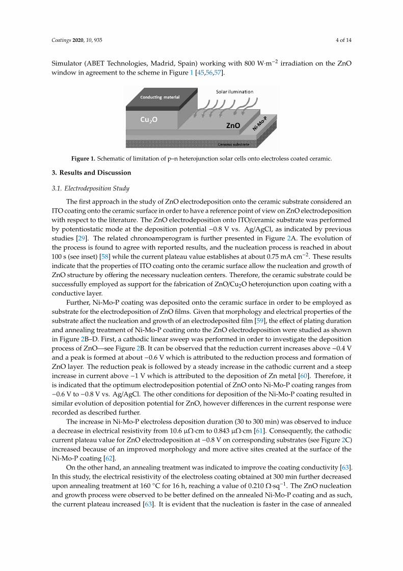
Simulator (ABET Technologies, Madrid, Spain) working with 800 W·m−2 irradiation on the ZnOwindow in agreement to the scheme in Figure 1 [45,56,57].Coatings 2020, 10, x FOR PEER REVIEW 4 of 14
Figure 1. Schematic of limitation of p–n heterojunction solar cells onto electroless coated ceramic.
3. Results and Discussion
3.1. Electrodeposition Study
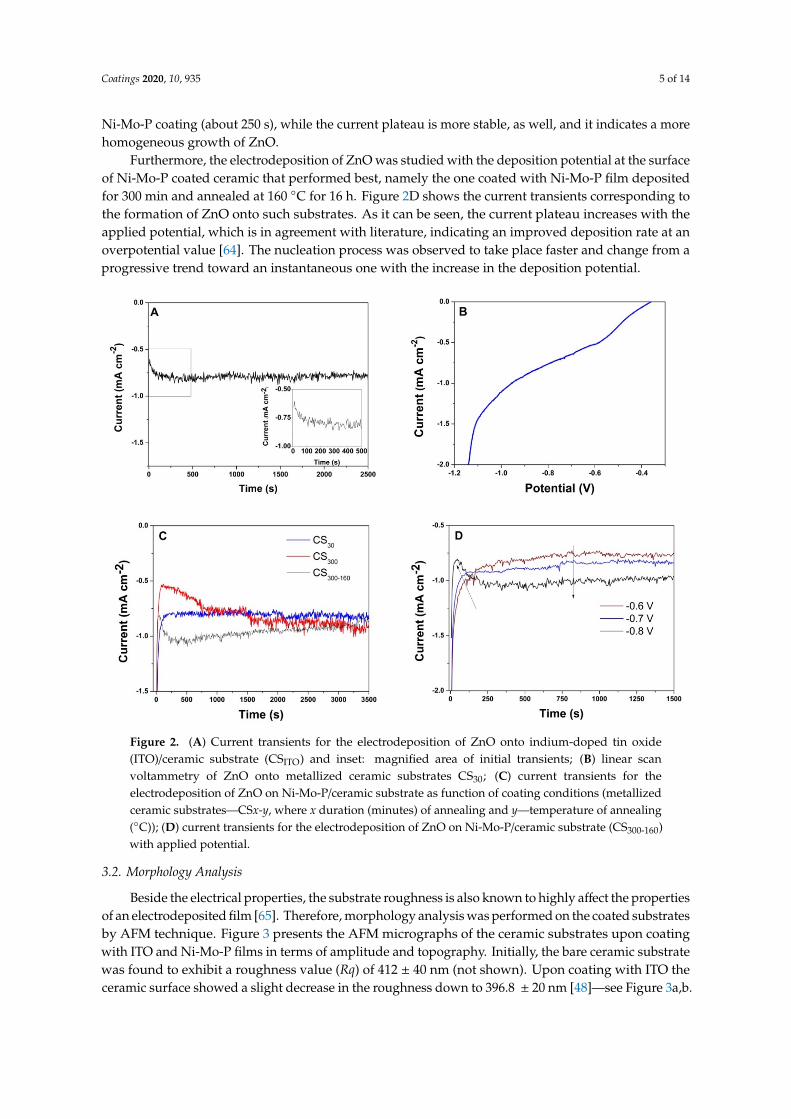
The first approach in the study of ZnO electrodeposition onto the ceramic substrate considered an ITO coating onto the ceramic surface in order to have a reference point of view on ZnO electrodeposition with respect to the literature. The ZnO electrodeposition onto ITO/ceramic substrate was performed by potentiostatic mode at the deposition potential −0.8 V vs. Ag/AgCl, as indicated by previous studies [29]. The related chronoamperogram is further presented in Figure 2A. The evolution of the process is found to agree with reported results, and the nucleation process is reached in about 100 s (see inset) [58] while the current plateau value establishes at about 0.75 mA cm−2. These results indicate that the properties of ITO coating onto the ceramic surface allow the nucleation and growth of ZnO structure by offering the necessary nucleation centers. Therefore, the ceramic substrate could be successfully employed as support for the fabrication of ZnO/Cu2O heterojunction upon coating with a conductive layer.
Further, Ni-Mo-P coating was deposited onto the ceramic surface in order to be employed as substrate for the electrodeposition of ZnO films. Given that morphology and electrical properties of the substrate affect the nucleation and growth of an electrodeposited film [59], the effect of plating duration and annealing treatment of Ni-Mo-P coating onto the ZnO electrodeposition were studied as shown in Figure 2B–D. First, a cathodic linear sweep was performed in order to investigate the deposition process of ZnO—see Figure 2B. It can be observed that the reduction current increases above −0.4 V and a peak is formed at about −0.6 V which is attributed to the reduction process and formation of ZnO layer. The reduction peak is followed by a steady increase in the cathodic current and a steep increase in current above −1 V which is attributed to the deposition of Zn metal [60]. Therefore, it is indicated that the optimum electrodeposition potential of ZnO onto Ni-Mo-P coating ranges from −0.6 V to −0.8 V vs. Ag/AgCl. The other conditions for deposition of the Ni-Mo-P coating resulted in similar evolution of deposition potential for ZnO, however differences in the current response were recorded as described further.
The increase in Ni-Mo-P electroless deposition duration (30 to 300 min) was observed to induce a decrease in electrical resistivity from 10.6 µΩ·cm to 0.843 µΩ·cm [61]. Consequently, the cathodic current plateau value for ZnO electrodeposition at −0.8 V on corresponding substrates (see Figure 2C) increased because of an improved morphology and more active sites created at the surface of the Ni-Mo-P coating [62].
On the other hand, an annealing treatment was indicated to improve the coating conductivity [63]. In this study, the electrical resistivity of the electroless coating obtained at 300 min further decreased upon annealing treatment at 160 °C for 16 h, reaching a value of 0.210 Ω·sq−1. The ZnO nucleation and growth process were observed to be better defined on the annealed Ni-Mo-P coating and as such, the current plateau increased [63]. It is evident that the nucleation is faster in the case of annealed Ni-Mo-P coating (about 250 s), while the current plateau is more stable, as well, and it indicates a more homogeneous growth of ZnO.
Figure 1. Schematic of limitation of p–n heterojunction solar cells onto electroless coated ceramic.
3. Results and Discussion
3.1. Electrodeposition Study
The first approach in the study of ZnO electrodeposition onto the ceramic substrate considered anITO coating onto the ceramic surface in order to have a reference point of view on ZnO electrodepositionwith respect to the literature. The ZnO electrodeposition onto ITO/ceramic substrate was performedby potentiostatic mode at the deposition potential −0.8 V vs. Ag/AgCl, as indicated by previousstudies [29]. The related chronoamperogram is further presented in Figure 2A. The evolution ofthe process is found to agree with reported results, and the nucleation process is reached in about100 s (see inset) [58] while the current plateau value establishes at about 0.75 mA cm−2. These resultsindicate that the properties of ITO coating onto the ceramic surface allow the nucleation and growth ofZnO structure by offering the necessary nucleation centers. Therefore, the ceramic substrate could besuccessfully employed as support for the fabrication of ZnO/Cu2O heterojunction upon coating with aconductive layer.
Further, Ni-Mo-P coating was deposited onto the ceramic surface in order to be employed assubstrate for the electrodeposition of ZnO films. Given that morphology and electrical properties of thesubstrate affect the nucleation and growth of an electrodeposited film [59], the effect of plating durationand annealing treatment of Ni-Mo-P coating onto the ZnO electrodeposition were studied as shownin Figure 2B–D. First, a cathodic linear sweep was performed in order to investigate the depositionprocess of ZnO—see Figure 2B. It can be observed that the reduction current increases above −0.4 Vand a peak is formed at about −0.6 V which is attributed to the reduction process and formation ofZnO layer. The reduction peak is followed by a steady increase in the cathodic current and a steepincrease in current above −1 V which is attributed to the deposition of Zn metal [60]. Therefore, itis indicated that the optimum electrodeposition potential of ZnO onto Ni-Mo-P coating ranges from−0.6 V to −0.8 V vs. Ag/AgCl. The other conditions for deposition of the Ni-Mo-P coating resulted insimilar evolution of deposition potential for ZnO, however differences in the current response wererecorded as described further.
The increase in Ni-Mo-P electroless deposition duration (30 to 300 min) was observed to inducea decrease in electrical resistivity from 10.6 µΩ·cm to 0.843 µΩ·cm [61]. Consequently, the cathodiccurrent plateau value for ZnO electrodeposition at −0.8 V on corresponding substrates (see Figure 2C)increased because of an improved morphology and more active sites created at the surface of theNi-Mo-P coating [62].
On the other hand, an annealing treatment was indicated to improve the coating conductivity [63].In this study, the electrical resistivity of the electroless coating obtained at 300 min further decreasedupon annealing treatment at 160 C for 16 h, reaching a value of 0.210 Ω·sq−1. The ZnO nucleationand growth process were observed to be better defined on the annealed Ni-Mo-P coating and as such,the current plateau increased [63]. It is evident that the nucleation is faster in the case of annealed
Coatings 2020, 10, 935 5 of 14
Ni-Mo-P coating (about 250 s), while the current plateau is more stable, as well, and it indicates a morehomogeneous growth of ZnO.
Furthermore, the electrodeposition of ZnO was studied with the deposition potential at the surfaceof Ni-Mo-P coated ceramic that performed best, namely the one coated with Ni-Mo-P film depositedfor 300 min and annealed at 160 C for 16 h. Figure 2D shows the current transients corresponding tothe formation of ZnO onto such substrates. As it can be seen, the current plateau increases with theapplied potential, which is in agreement with literature, indicating an improved deposition rate at anoverpotential value [64]. The nucleation process was observed to take place faster and change from aprogressive trend toward an instantaneous one with the increase in the deposition potential.Coatings 2020, 10, x FOR PEER REVIEW 5 of 14
Figure 2. (A) Current transients for the electrodeposition of ZnO onto indium-doped tin oxide (ITO)/ceramic substrate (CSITO) and inset: magnified area of initial transients; (B) linear scan voltammetry of ZnO onto metallized ceramic substrates CS30; (C) current transients for the electrodeposition of ZnO on Ni-Mo-P/ceramic substrate as function of coating conditions (metallized ceramic substrates—CSx-y, where x duration (minutes) of annealing and y—temperature of annealing (°C)); (D) current transients for the electrodeposition of ZnO on Ni-Mo-P/ceramic substrate (CS300-160) with applied potential.
Furthermore, the electrodeposition of ZnO was studied with the deposition potential at the surface of Ni-Mo-P coated ceramic that performed best, namely the one coated with Ni-Mo-P film deposited for 300 min and annealed at 160 °C for 16 h. Figure 2D shows the current transients corresponding to the formation of ZnO onto such substrates. As it can be seen, the current plateau increases with the applied potential, which is in agreement with literature, indicating an improved deposition rate at an overpotential value [64]. The nucleation process was observed to take place faster and change from a progressive trend toward an instantaneous one with the increase in the deposition potential.
3.2. Morphology Analysis
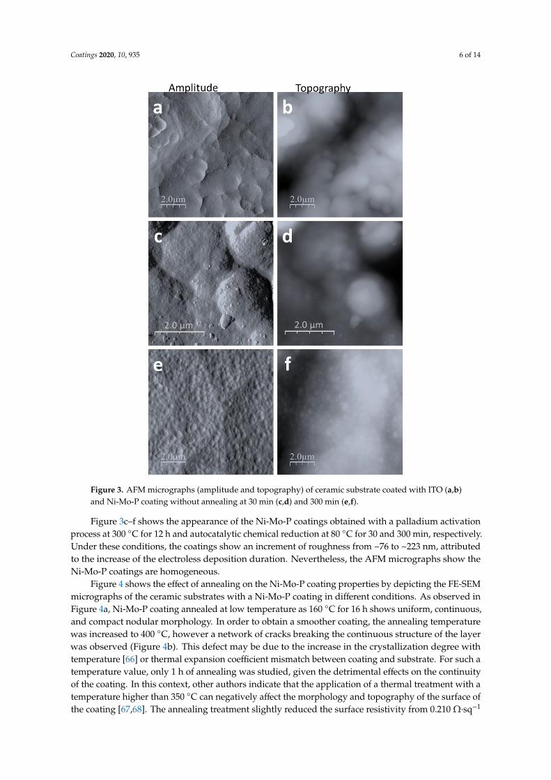
Beside the electrical properties, the substrate roughness is also known to highly affect the properties of an electrodeposited film [65]. Therefore, morphology analysis was performed on the coated substrates by AFM technique. Figure 3 presents the AFM micrographs of the ceramic substrates upon coating with ITO and Ni-Mo-P films in terms of amplitude and topography. Initially, the bare ceramic substrate was found to exhibit a roughness value (Rq) of 412 ± 40 nm (not shown). Upon coating with ITO the ceramic surface showed a slight decrease in the roughness down to 396.8 ± 20 nm [48]—see Figure 3a,b.
Figure 2. (A) Current transients for the electrodeposition of ZnO onto indium-doped tin oxide(ITO)/ceramic substrate (CSITO) and inset: magnified area of initial transients; (B) linear scanvoltammetry of ZnO onto metallized ceramic substrates CS30; (C) current transients for theelectrodeposition of ZnO on Ni-Mo-P/ceramic substrate as function of coating conditions (metallizedceramic substrates—CSx-y, where x duration (minutes) of annealing and y—temperature of annealing(C)); (D) current transients for the electrodeposition of ZnO on Ni-Mo-P/ceramic substrate (CS300-160)with applied potential.
3.2. Morphology Analysis
Beside the electrical properties, the substrate roughness is also known to highly affect the propertiesof an electrodeposited film [65]. Therefore, morphology analysis was performed on the coated substratesby AFM technique. Figure 3 presents the AFM micrographs of the ceramic substrates upon coatingwith ITO and Ni-Mo-P films in terms of amplitude and topography. Initially, the bare ceramic substratewas found to exhibit a roughness value (Rq) of 412 ± 40 nm (not shown). Upon coating with ITO theceramic surface showed a slight decrease in the roughness down to 396.8 ± 20 nm [48]—see Figure 3a,b.
Coatings 2020, 10, 935 6 of 14Coatings 2020, 10, x FOR PEER REVIEW 6 of 14
Figure 3. AFM micrographs (amplitude and topography) of ceramic substrate coated with ITO (a,b) and Ni-Mo-P coating without annealing at 30 min (c,d) and 300 min (e,f).
Figure 3c–f shows the appearance of the Ni-Mo-P coatings obtained with a palladium activation process at 300 °C for 12 h and autocatalytic chemical reduction at 80 °C for 30 and 300 min, respectively. Under these conditions, the coatings show an increment of roughness from ~76 to ~223 nm, attributed to the increase of the electroless deposition duration. Nevertheless, the AFM micrographs show the Ni-Mo-P coatings are homogeneous.
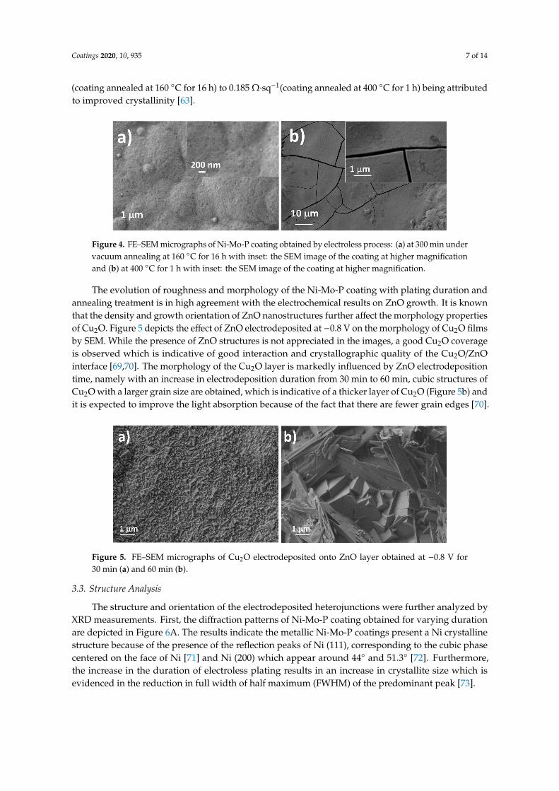
Figure 4 shows the effect of annealing on the Ni-Mo-P coating properties by depicting the FE-SEM micrographs of the ceramic substrates with a Ni-Mo-P coating in different conditions. As observed in Figure 4a, Ni-Mo-P coating annealed at low temperature as 160 °C for 16 h shows uniform, continuous, and compact nodular morphology. In order to obtain a smoother coating, the annealing temperature was increased to 400 °C, however a network of cracks breaking the continuous structure of the layer was observed (Figure 4b). This defect may be due to the increase in the crystallization degree with temperature [66] or thermal expansion coefficient mismatch between coating and substrate. For such a temperature value, only 1 h of annealing was studied, given the detrimental effects on the continuity of the coating. In this context, other authors indicate that the application of a thermal treatment with a temperature higher than 350 °C can negatively affect the morphology and topography of the surface of the coating [67,68]. The annealing treatment slightly
Figure 3. AFM micrographs (amplitude and topography) of ceramic substrate coated with ITO (a,b)and Ni-Mo-P coating without annealing at 30 min (c,d) and 300 min (e,f).
Figure 3c–f shows the appearance of the Ni-Mo-P coatings obtained with a palladium activationprocess at 300 C for 12 h and autocatalytic chemical reduction at 80 C for 30 and 300 min, respectively.Under these conditions, the coatings show an increment of roughness from ~76 to ~223 nm, attributedto the increase of the electroless deposition duration. Nevertheless, the AFM micrographs show theNi-Mo-P coatings are homogeneous.
Figure 4 shows the effect of annealing on the Ni-Mo-P coating properties by depicting the FE-SEMmicrographs of the ceramic substrates with a Ni-Mo-P coating in different conditions. As observed inFigure 4a, Ni-Mo-P coating annealed at low temperature as 160 C for 16 h shows uniform, continuous,and compact nodular morphology. In order to obtain a smoother coating, the annealing temperaturewas increased to 400 C, however a network of cracks breaking the continuous structure of the layerwas observed (Figure 4b). This defect may be due to the increase in the crystallization degree withtemperature [66] or thermal expansion coefficient mismatch between coating and substrate. For such atemperature value, only 1 h of annealing was studied, given the detrimental effects on the continuityof the coating. In this context, other authors indicate that the application of a thermal treatment with atemperature higher than 350 C can negatively affect the morphology and topography of the surface ofthe coating [67,68]. The annealing treatment slightly reduced the surface resistivity from 0.210 Ω·sq−1
Coatings 2020, 10, 935 7 of 14
(coating annealed at 160 C for 16 h) to 0.185 Ω·sq−1(coating annealed at 400 C for 1 h) being attributedto improved crystallinity [63].
Coatings 2020, 10, x FOR PEER REVIEW 7 of 14
reduced the surface resistivity from 0.210 Ω·sq−1 (coating annealed at 160 °C for 16 h) to 0.185 Ω·sq−1(coating annealed at 400 °C for 1 h) being attributed to improved crystallinity [63].
Figure 4. FE–SEM micrographs of Ni-Mo-P coating obtained by electroless process: (a) at 300 min under vacuum annealing at 160 °C for 16 h with inset: the SEM image of the coating at higher magnification and (b) at 400 °C for 1 h with inset: the SEM image of the coating at higher magnification.
The evolution of roughness and morphology of the Ni-Mo-P coating with plating duration and annealing treatment is in high agreement with the electrochemical results on ZnO growth. It is known that the density and growth orientation of ZnO nanostructures further affect the morphology properties of Cu2O. Figure 5 depicts the effect of ZnO electrodeposited at −0.8 V on the morphology of Cu2O films by SEM. While the presence of ZnO structures is not appreciated in the images, a good Cu2O coverage is observed which is indicative of good interaction and crystallographic quality of the Cu2O/ZnO interface [69,70]. The morphology of the Cu2O layer is markedly influenced by ZnO electrodeposition time, namely with an increase in electrodeposition duration from 30 min to 60 min, cubic structures of Cu2O with a larger grain size are obtained, which is indicative of a thicker layer of Cu2O (Figure 5b) and it is expected to improve the light absorption because of the fact that there are fewer grain edges [70].
Figure 5. FE–SEM micrographs of Cu2O electrodeposited onto ZnO layer obtained at −0.8 V for 30 min (a) and 60 min (b).
3.3. Structure Analysis
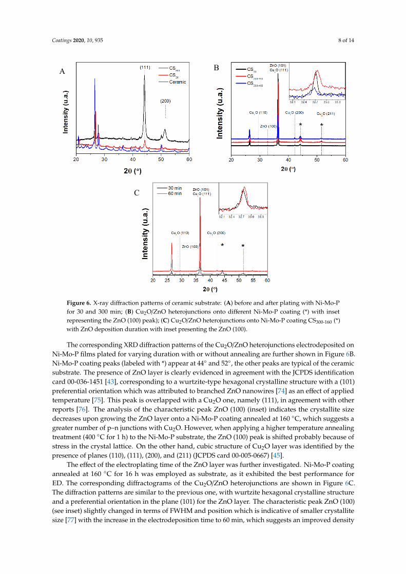
The structure and orientation of the electrodeposited heterojunctions were further analyzed by XRD measurements. First, the diffraction patterns of Ni-Mo-P coating obtained for varying duration are depicted in Figure 6A. The results indicate the metallic Ni-Mo-P coatings present a Ni crystalline structure because of the presence of the reflection peaks of Ni (111), corresponding to the cubic phase centered on the face of Ni [71] and Ni (200) which appear around 44° and 51.3° [72]. Furthermore, the increase in the duration of electroless plating results in an increase in crystallite size which is evidenced in the reduction in full width of half maximum (FWHM) of the predominant peak [73].
The corresponding XRD diffraction patterns of the Cu2O/ZnO heterojunctions electrodeposited on Ni-Mo-P films plated for varying duration with or without annealing are further shown in Figure
Figure 4. FE–SEM micrographs of Ni-Mo-P coating obtained by electroless process: (a) at 300 min undervacuum annealing at 160 C for 16 h with inset: the SEM image of the coating at higher magnificationand (b) at 400 C for 1 h with inset: the SEM image of the coating at higher magnification.
The evolution of roughness and morphology of the Ni-Mo-P coating with plating duration andannealing treatment is in high agreement with the electrochemical results on ZnO growth. It is knownthat the density and growth orientation of ZnO nanostructures further affect the morphology propertiesof Cu2O. Figure 5 depicts the effect of ZnO electrodeposited at −0.8 V on the morphology of Cu2O filmsby SEM. While the presence of ZnO structures is not appreciated in the images, a good Cu2O coverageis observed which is indicative of good interaction and crystallographic quality of the Cu2O/ZnOinterface [69,70]. The morphology of the Cu2O layer is markedly influenced by ZnO electrodepositiontime, namely with an increase in electrodeposition duration from 30 min to 60 min, cubic structures ofCu2O with a larger grain size are obtained, which is indicative of a thicker layer of Cu2O (Figure 5b) andit is expected to improve the light absorption because of the fact that there are fewer grain edges [70].
Coatings 2020, 10, x FOR PEER REVIEW 7 of 14
reduced the surface resistivity from 0.210 Ω·sq−1 (coating annealed at 160 °C for 16 h) to 0.185 Ω·sq−1(coating annealed at 400 °C for 1 h) being attributed to improved crystallinity [63].
Figure 4. FE–SEM micrographs of Ni-Mo-P coating obtained by electroless process: (a) at 300 min under vacuum annealing at 160 °C for 16 h with inset: the SEM image of the coating at higher magnification and (b) at 400 °C for 1 h with inset: the SEM image of the coating at higher magnification.
The evolution of roughness and morphology of the Ni-Mo-P coating with plating duration and annealing treatment is in high agreement with the electrochemical results on ZnO growth. It is known that the density and growth orientation of ZnO nanostructures further affect the morphology properties of Cu2O. Figure 5 depicts the effect of ZnO electrodeposited at −0.8 V on the morphology of Cu2O films by SEM. While the presence of ZnO structures is not appreciated in the images, a good Cu2O coverage is observed which is indicative of good interaction and crystallographic quality of the Cu2O/ZnO interface [69,70]. The morphology of the Cu2O layer is markedly influenced by ZnO electrodeposition time, namely with an increase in electrodeposition duration from 30 min to 60 min, cubic structures of Cu2O with a larger grain size are obtained, which is indicative of a thicker layer of Cu2O (Figure 5b) and it is expected to improve the light absorption because of the fact that there are fewer grain edges [70].
Figure 5. FE–SEM micrographs of Cu2O electrodeposited onto ZnO layer obtained at −0.8 V for 30 min (a) and 60 min (b).
3.3. Structure Analysis
The structure and orientation of the electrodeposited heterojunctions were further analyzed by XRD measurements. First, the diffraction patterns of Ni-Mo-P coating obtained for varying duration are depicted in Figure 6A. The results indicate the metallic Ni-Mo-P coatings present a Ni crystalline structure because of the presence of the reflection peaks of Ni (111), corresponding to the cubic phase centered on the face of Ni [71] and Ni (200) which appear around 44° and 51.3° [72]. Furthermore, the increase in the duration of electroless plating results in an increase in crystallite size which is evidenced in the reduction in full width of half maximum (FWHM) of the predominant peak [73].
The corresponding XRD diffraction patterns of the Cu2O/ZnO heterojunctions electrodeposited on Ni-Mo-P films plated for varying duration with or without annealing are further shown in Figure
Figure 5. FE–SEM micrographs of Cu2O electrodeposited onto ZnO layer obtained at −0.8 V for30 min (a) and 60 min (b).
3.3. Structure Analysis
The structure and orientation of the electrodeposited heterojunctions were further analyzed byXRD measurements. First, the diffraction patterns of Ni-Mo-P coating obtained for varying durationare depicted in Figure 6A. The results indicate the metallic Ni-Mo-P coatings present a Ni crystallinestructure because of the presence of the reflection peaks of Ni (111), corresponding to the cubic phasecentered on the face of Ni [71] and Ni (200) which appear around 44 and 51.3 [72]. Furthermore,the increase in the duration of electroless plating results in an increase in crystallite size which isevidenced in the reduction in full width of half maximum (FWHM) of the predominant peak [73].
Coatings 2020, 10, 935 8 of 14
Coatings 2020, 10, x FOR PEER REVIEW 8 of 14
6B. Ni-Mo-P coating peaks (labeled with *) appear at 44° and 52°, the other peaks are typical of the ceramic substrate. The presence of ZnO layer is clearly evidenced in agreement with the JCPDS identification card 00-036-1451 [43], corresponding to a wurtzite-type hexagonal crystalline structure with a (101) preferential orientation which was attributed to branched ZnO nanowires [74] as an effect of applied temperature [75]. This peak is overlapped with a Cu2O one, namely (111), in agreement with other reports [76]. The analysis of the characteristic peak ZnO (100) (inset) indicates the crystallite size decreases upon growing the ZnO layer onto a Ni-Mo-P coating annealed at 160 °C, which suggests a greater number of p–n junctions with Cu2O. However, when applying a higher temperature annealing treatment (400 °C for 1 h) to the Ni-Mo-P substrate, the ZnO (100) peak is shifted probably because of stress in the crystal lattice. On the other hand, cubic structure of Cu2O layer was identified by the presence of planes (110), (111), (200), and (211) (JCPDS card 00-005-0667) [45].
Figure 6. X-ray diffraction patterns of ceramic substrate: (A) before and after plating with Ni-Mo-P for 30 and 300 min; (B) Cu2O/ZnO heterojunctions onto different Ni-Mo-P coating (*) with inset representing the ZnO (100) peak); (C) Cu2O/ZnO heterojunctions onto Ni-Mo-P coating CS300-160 (*) with ZnO deposition duration with inset presenting the ZnO (100).
The effect of the electroplating time of the ZnO layer was further investigated. Ni-Mo-P coating annealed at 160 °C for 16 h was employed as substrate, as it exhibited the best performance for ED. The corresponding diffractograms of the Cu2O/ZnO heterojunctions are shown in Figure 6C. The diffraction patterns are similar to the previous one, with wurtzite hexagonal crystalline structure and a preferential orientation in the plane (101) for the ZnO layer. The characteristic peak ZnO (100) (see inset) slightly changed in terms of FWHM and position which is indicative of smaller crystallite size [77] with the increase in the electrodeposition time to 60 min, which suggests an improved density of heterojunctions [29,78,79]. Regarding the synthesized Cu2O layers, they showed similar pattern as previously shown with the previous samples.
A B
C
Figure 6. X-ray diffraction patterns of ceramic substrate: (A) before and after plating with Ni-Mo-Pfor 30 and 300 min; (B) Cu2O/ZnO heterojunctions onto different Ni-Mo-P coating (*) with insetrepresenting the ZnO (100) peak); (C) Cu2O/ZnO heterojunctions onto Ni-Mo-P coating CS300-160 (*)with ZnO deposition duration with inset presenting the ZnO (100).
The corresponding XRD diffraction patterns of the Cu2O/ZnO heterojunctions electrodeposited onNi-Mo-P films plated for varying duration with or without annealing are further shown in Figure 6B.Ni-Mo-P coating peaks (labeled with *) appear at 44 and 52, the other peaks are typical of the ceramicsubstrate. The presence of ZnO layer is clearly evidenced in agreement with the JCPDS identificationcard 00-036-1451 [43], corresponding to a wurtzite-type hexagonal crystalline structure with a (101)preferential orientation which was attributed to branched ZnO nanowires [74] as an effect of appliedtemperature [75]. This peak is overlapped with a Cu2O one, namely (111), in agreement with otherreports [76]. The analysis of the characteristic peak ZnO (100) (inset) indicates the crystallite sizedecreases upon growing the ZnO layer onto a Ni-Mo-P coating annealed at 160 C, which suggests agreater number of p–n junctions with Cu2O. However, when applying a higher temperature annealingtreatment (400 C for 1 h) to the Ni-Mo-P substrate, the ZnO (100) peak is shifted probably because ofstress in the crystal lattice. On the other hand, cubic structure of Cu2O layer was identified by thepresence of planes (110), (111), (200), and (211) (JCPDS card 00-005-0667) [45].
The effect of the electroplating time of the ZnO layer was further investigated. Ni-Mo-P coatingannealed at 160 C for 16 h was employed as substrate, as it exhibited the best performance forED. The corresponding diffractograms of the Cu2O/ZnO heterojunctions are shown in Figure 6C.The diffraction patterns are similar to the previous one, with wurtzite hexagonal crystalline structureand a preferential orientation in the plane (101) for the ZnO layer. The characteristic peak ZnO (100)(see inset) slightly changed in terms of FWHM and position which is indicative of smaller crystallitesize [77] with the increase in the electrodeposition time to 60 min, which suggests an improved density
Coatings 2020, 10, 935 9 of 14
of heterojunctions [29,78,79]. Regarding the synthesized Cu2O layers, they showed similar pattern aspreviously shown with the previous samples.
3.4. Photoelectical Properties of Cu2O/ZnO Heterojunction Solar Cells Supported ontoNi-Mo-P-Coated Ceramic
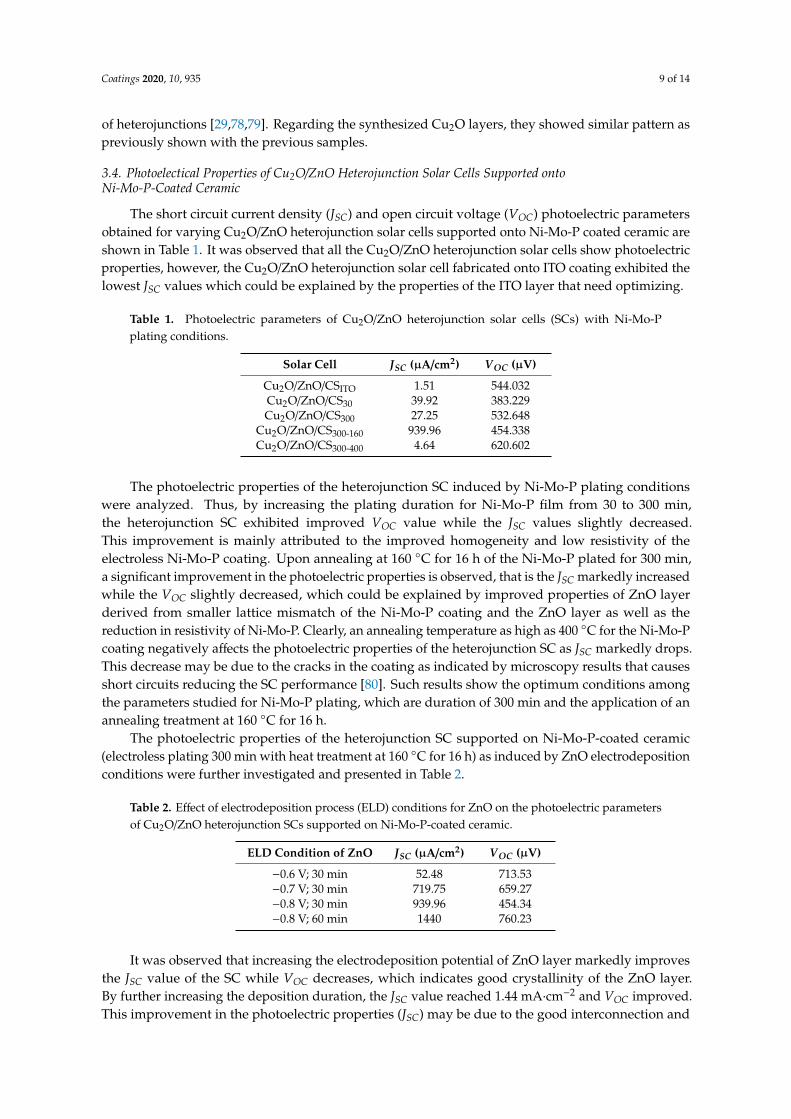
The short circuit current density (JSC) and open circuit voltage (VOC) photoelectric parametersobtained for varying Cu2O/ZnO heterojunction solar cells supported onto Ni-Mo-P coated ceramic areshown in Table 1. It was observed that all the Cu2O/ZnO heterojunction solar cells show photoelectricproperties, however, the Cu2O/ZnO heterojunction solar cell fabricated onto ITO coating exhibited thelowest JSC values which could be explained by the properties of the ITO layer that need optimizing.
Table 1. Photoelectric parameters of Cu2O/ZnO heterojunction solar cells (SCs) with Ni-Mo-Pplating conditions.
Solar Cell JSC (µA/cm2) VOC (µV)
Cu2O/ZnO/CSITO 1.51 544.032Cu2O/ZnO/CS30 39.92 383.229Cu2O/ZnO/CS300 27.25 532.648
Cu2O/ZnO/CS300-160 939.96 454.338Cu2O/ZnO/CS300-400 4.64 620.602
The photoelectric properties of the heterojunction SC induced by Ni-Mo-P plating conditionswere analyzed. Thus, by increasing the plating duration for Ni-Mo-P film from 30 to 300 min,the heterojunction SC exhibited improved VOC value while the JSC values slightly decreased.This improvement is mainly attributed to the improved homogeneity and low resistivity of theelectroless Ni-Mo-P coating. Upon annealing at 160 C for 16 h of the Ni-Mo-P plated for 300 min,a significant improvement in the photoelectric properties is observed, that is the JSC markedly increasedwhile the VOC slightly decreased, which could be explained by improved properties of ZnO layerderived from smaller lattice mismatch of the Ni-Mo-P coating and the ZnO layer as well as thereduction in resistivity of Ni-Mo-P. Clearly, an annealing temperature as high as 400 C for the Ni-Mo-Pcoating negatively affects the photoelectric properties of the heterojunction SC as JSC markedly drops.This decrease may be due to the cracks in the coating as indicated by microscopy results that causesshort circuits reducing the SC performance [80]. Such results show the optimum conditions amongthe parameters studied for Ni-Mo-P plating, which are duration of 300 min and the application of anannealing treatment at 160 C for 16 h.
The photoelectric properties of the heterojunction SC supported on Ni-Mo-P-coated ceramic(electroless plating 300 min with heat treatment at 160 C for 16 h) as induced by ZnO electrodepositionconditions were further investigated and presented in Table 2.
Table 2. Effect of electrodeposition process (ELD) conditions for ZnO on the photoelectric parametersof Cu2O/ZnO heterojunction SCs supported on Ni-Mo-P-coated ceramic.
ELD Condition of ZnO JSC (µA/cm2) VOC (µV)
−0.6 V; 30 min 52.48 713.53−0.7 V; 30 min 719.75 659.27−0.8 V; 30 min 939.96 454.34−0.8 V; 60 min 1440 760.23
It was observed that increasing the electrodeposition potential of ZnO layer markedly improvesthe JSC value of the SC while VOC decreases, which indicates good crystallinity of the ZnO layer.By further increasing the deposition duration, the JSC value reached 1.44 mA·cm−2 and VOC improved.This improvement in the photoelectric properties (JSC) may be due to the good interconnection and
Coatings 2020, 10, 935 10 of 14
crystallographic quality of the Cu2O/ZnO interface and improved properties of ZnO nanostructuressuch as density and aspect ratio that could improve charge transport [69]. The increase in VOC value isan indication of reduced grain limits and improved light absorption [70].
4. Conclusions
A ZnO/Cu2O heterojunction type solar cell was fabricated onto ceramic substrate by simpleelectrodeposition technique. The electrical functionalization of the ceramic surface has been achievedby electroless coating of a Ni-Mo-P film. Continuous and homogeneous Ni-Mo-P coatings wereobtained with typical XRD reflection planes. The results indicated the morphology and electricalconductivity of Ni-Mo-P film can be easily tailored by adjusting the electroless coating conditionssuch as duration and by applying an appropriate annealing treatment, namely lower temperaturefor long time. The increase in applied potential and duration for ZnO electrodeposition, namely−0.8 V for 1 h resulted in the best performance of the ZnO/Cu2O heterojunction type solar cell, thatis, 1.44 mA·cm−2 for the JSC and 760.23 µV for the VOC value, respectively, which demonstrates theimportance of electrodeposition of ZnO layer toward improving the photoelectrical parameters ofthe heterojunction solar cell. Although the performance still need improvements of the photoelectricparameters, the obtained results show that an insulating substrate (in this case a ceramic tile) could beused for electrical power generation applications by applying a Ni-Mo-P electroless coating. The resultsof this work indicate that optimized electrochemical growth of the heterojunction layers, annealingtreatment, and the tailoring of the ZnO/Cu2O interface are parameters of paramount importance forsolar cell performance improvement.
Author Contributions: Conceptualization, N.M.R.-L., A.I.P., J.C.; methodology, N.M.R.-L. and A.I.P.; investigation,N.M.R.-L., A.I.P., J.C., and D.B.-M.; data curation, N.M.R.-L. and A.I.P.; writing—original draft preparation,N.M.R.-L.; writing—review and editing, N.M.R.-L., A.I.P., J.C., and D.B.-M. All authors have read and agreed tothe published version of the manuscript.
Funding: This research received no external funding.
Acknowledgments: The technical support from Servicio de Microscopía Electrónica, UPV and InstitutoUniversitario de Tecnología Nanofotónica, UPV is highly acknowledged.
Conflicts of Interest: The authors declare no conflict of interest.
References
1. Kishawy, H.A.; Hosseini, A. Machining Difficult-to-Cut Materials; Materials Forming, Machining and Tribology;Springer International Publishing: Cham, Switzerland, 2019; ISBN 978-3-319-95965-8.
2. Leali, P.T.; Merolli, A. Fundamentals of Biomaterials. In Biomaterials in Hand Surgery; Springer Milan: Milano,Italy, 2009; pp. 1–11. ISBN 9788847011946.
3. Ghosh, S.; Pal, K.S.; Dandapat, N.; Datta, S.; Basu, D. Interfacial properties of metallized alumina ceramics.Met. Mater. Int. 2012, 18, 625–630. [CrossRef]
4. Ene Hourdequin, H.; Laudebat, L.; Locatelli, M.-L.; Valdez-Nava, Z.; Bidan, P. Metallized ceramic substratewith mesa structure for voltage ramp-up of power modules. Eur. Phys. J. Appl. Phys 2019, 87, 20903.[CrossRef]
5. Mirone, G.; Sitta, A.; D’Arrigo, G.; Calabretta, M. Material Characterization and Warpage Modeling for PowerDevices Active Metal Brazed Substrates. IEEE Trans. Device Mater. Reliab. 2019, 19, 537–542. [CrossRef]
6. Sampaio, P.G.V.; Gonzï¿ 12 lez, M.O.A. Photovoltaic solar energy: Conceptual framework. Renew. Sustain.
Energy Rev. 2017, 74, 590–601. [CrossRef]7. Agarwala, R.C.; Agarwala, V. Electroless alloy/composite coatings: A review. Sadhana 2003, 28, 475–493.
[CrossRef]8. Rosas-Laverde, N.M.; Pruna, A.; Cembrero, J.; Pascual, M.; Orozco-Messana, J. Optimizing Electroless Plating
of Ni–Mo–P Coatings Toward Functional Ceramics. Acta Metall. Sin. Engl. Lett. 2020, 33, 1–9. [CrossRef]
Coatings 2020, 10, 935 11 of 14
9. Badán, J.A.; Navarrete-Astorga, E.; Henríquez, R.; Martín, F.; Marotti, R.E.; Ramos-Barrado, J.R.; Dalchiele, E.A.Optical properties of silver nanoparticles deposited onto silicon substrates by different soft-solution processingtechniques. Opt. Mater. (Amst) 2020, 100, 109651. [CrossRef]
10. Ma, H.; Liu, Z.; Wu, L.; Wang, Y.; Wang, X. Study of a pre-treatment process for electroless copper plating onceramics. Thin Solid Films 2011, 519, 7860–7863. [CrossRef]
11. Zhang, B. Electroless Plating Baths of Metals, Binary Alloys, and Multicomponent Alloys. In Amorphousand Nano Alloys Electroless Depositions: Technology, Composition. Structure and Theory; Tian, S., Ed.; Elsevier:Amsterdam, The Netherlands, 2016; pp. 51–106. ISBN 9780128026854.
12. Zhang, B. Impact Parameters and Deposition Rate. In Amorphous and Nano Alloys Electroless Depositions:Technology, Composition. Structure and Theory; Tian, S., Ed.; Elsevier: Amsterdam, The Netherlands, 2016;pp. 323–381. ISBN 9780128026854.
13. Heidarzadeh, A.; Mousavian, R.T.; Khosroshahi, R.A.; Afkham, Y.A.; Pouraliakbar, H. Empirical model topredict mass gain of cobalt electroless deposition on ceramic particles using response surface methodology.Rare Met. 2017, 36, 209–219. [CrossRef]
14. Zhou, R.; Chen, H.; Xu, C.; Hou, X.; Liu, G.; Liu, Y. Facile synthesis of electromagnetic Ni@glass fibercomposites via electroless deposition method. J. Mater. Sci. Mater. Electron. 2015, 26, 3530–3537. [CrossRef]
15. Tai, Y.; Chen, H.; Xu, C.; Liu, Y. Conductive glass fabrics@nickel composites prepared by a facile electrolessdeposition method. Mater. Lett. 2016, 171, 158–161. [CrossRef]
16. Lee, C.-L.; Wan, C.-C.; Wang, Y.-Y. Pd Nanoparticles as a New Activator for Electroless Copper Deposition. J.Electrochem. Soc. 2003, 150, C125. [CrossRef]
17. Lin, J.D.; Kuo, C.L. Effects of hydrogen plasma treatment on microstructure evolution and electricalconductivity of electroless Ni-P coatings on polyimide and glass substrates. Surf. Coatings Technol. 2012, 209,80–89. [CrossRef]
18. Kazemi, A.; Yang, S. Atomistic Study of the Effect of Magnesium Dopants on the Strength of NanocrystallineAluminum. JOM 2019, 71, 1209–1214. [CrossRef]
19. Li, Q.; Xu, M.; Fan, H.; Wang, H.; Peng, B.; Long, C.; Zhai, Y. Dielectric properties investigation of Cu2O/ZnOheterojunction thin films by electrodeposition. Mater. Sci. Eng. B Solid-State Mater. Adv. Technol. 2013, 178,496–501. [CrossRef]
20. Li, J.; Li, H.; Xue, Y.; Fang, H.; Wang, W. Facile electrodeposition of environment-friendly Cu2O/ZnOheterojunction for robust photoelectrochemical biosensing. Sensors Actuators B Chem. 2014, 191, 619–624.[CrossRef]
21. Bhattacharya, R.N.; Deb, S.K. A Low-Cost Approach to Fabrication of Multinary Compounds forEnergy-Related Applications. Jpn. J. Appl. Phys. 2000, 39, 424. [CrossRef]
22. Kang, D.; Lee, D.; Choi, K.-S. Electrochemical Synthesis of Highly Oriented, Transparent, and Pinhole-FreeZnO and Al-Doped ZnO Films and Their Use in Heterojunction Solar Cells. Langmuir 2016, 32, 10459–10466.[CrossRef]
23. Shah, A.V.; Schade, H.; Vanecek, M.; Meier, J.; Vallat-Sauvain, E.; Wyrsch, N.; Kroll, U.; Droz, C.; Bailat, J.Thin-film silicon solar cell technology. Prog. Photovoltaics Res. Appl. 2004, 12, 113–142. [CrossRef]
24. Rosa, G.; Bosio, A.; Menossi, D.; Romeo, N. How the Starting Precursor Influences the Properties ofPolycrystalline CuInGaSe2 Thin Films Prepared by Sputtering and Selenization. Energies 2016, 9, 354.[CrossRef]
25. Calvet, I.; Barrachina, E.; Martí, R.; Fraga, D.; Stoyanova Lyubenova, T.; Carda, J.B. Development ofphotovoltaic ceramic tile based on CZTSSe absorber. Mater. Lett. 2015, 161, 636–639. [CrossRef]
26. Lin, S.; Li, X.X.; Pan, H.; Chen, H.; Li, X.X.; Li, Y.; Zhou, J. Numerical analysis of InxGa1-xN/SnS andAlxGa1-xN/SnS heterojunction solar cells. Energy Convers. Manag. 2016, 119, 361–367. [CrossRef]
27. Cheng, K.; Li, Q.; Meng, J.; Han, X.; Wu, Y.; Wang, S.; Qian, L.; Du, Z. Interface engineering for efficientcharge collection in Cu2O/ZnO heterojunction solar cells with ordered ZnO cavity-like nanopatterns. Sol.Energy Mater. Sol. Cells 2013, 116, 120–125. [CrossRef]
28. Reinders, A.; Verlinden, P.; Van Sark, W.; Freundlich, A. (Eds.) Photovoltaic Solar Energy; John Wiley & Sons,Ltd.: Chichester, UK, 2016; ISBN 9781118927496.
29. Rosas-Laverde, N.M.; Pruna, A.; Cembrero, J.; Orozco-Messana, J.; Manjón, F.J. Performance of grapheneoxide-modified electrodeposited ZnO/Cu2O heterojunction solar cells. Boletín Soc. Española Cerámica Vidr.2019, 58, 263–273. [CrossRef]
Coatings 2020, 10, 935 12 of 14
30. Rosas-Laverde, N.M.; Pruna, A.; Busquets-Mataix, D.; Marí, B.; Cembrero, J.; Salas Vicente, F.;Orozco-Messana, J. Improving the properties of Cu2O/ZnO heterojunction for photovoltaic application bygraphene oxide. Ceram. Int. 2018, 44, 23045–23051. [CrossRef]
31. Wang, C.; Xu, J.; Shi, S.; Zhang, Y.; Gao, Y.; Liu, Z.; Zhang, X.; Li, L. Optimizing performance of Cu2O/ZnOnanorods heterojunction based self-powered photodetector with ZnO seed layer. J. Phys. Chem. Solids 2017,103, 218–223. [CrossRef]
32. Elfadill, N.G.; Hashim, M.R.; Chahrour, K.M.; Qaeed, M.A.; Bououdina, M. The influence of Cu2O crystalstructure on the Cu2O/ZnO heterojunction photovoltaic performance. Superlattices Microstruct. 2015, 85,908–917. [CrossRef]
33. Bai, Z.; Zhang, Y. Self-powered UV-visible photodetectors based on ZnO/Cu2O nanowire/electrolyteheterojunctions. J. Alloys Compd. 2016, 675, 325–330. [CrossRef]
34. Bai, Z.; Liu, J.; Liu, F.; Zhang, Y. Enhanced photoresponse performance of self-powered UV–visiblephotodetectors based on ZnO/Cu2O/electrolyte heterojunctions via graphene incorporation. J. Alloys Compd.2017, 726, 803–809. [CrossRef]
35. Tran, M.H.; Cho, J.Y.; Sinha, S.; Gang, M.G.; Heo, J. Cu2O/ZnO heterojunction thin-film solar cells: The effectof electrodeposition condition and thickness of Cu2O. Thin Solid Films 2018, 661, 132–136. [CrossRef]
36. Messaoudi, O.; Makhlouf, H.; Souissi, A.; Ben assaker, I.; Amiri, G.; Bardaoui, A.; Oueslati, M.; Bechelany, M.;Chtourou, R. Synthesis and characterization of ZnO/Cu2O core–shell nanowires grown by two-stepelectrodeposition method. Appl. Surf. Sci. 2015, 343, 148–152. [CrossRef]
37. Jiang, X.; Lin, Q.; Zhang, M.; He, G.; Sun, Z. Microstructure, optical properties, and catalytic performance ofCu2O-modified ZnO nanorods prepared by electrodeposition. Nanoscale Res. Lett. 2015, 2–7. [CrossRef][PubMed]
38. Chen, J.W.; Perng, D.C.; Fang, J.F. Nano-structured Cu2O solar cells fabricated on sparse ZnO nanorods. Sol.Energy Mater. Sol. Cells 2011, 95, 2471–2477. [CrossRef]
39. Panigrahi, S.; Nunes, D.; Calmeiro, T.; Kardarian, K.; Martins, R.; Fortunato, E. Oxide-Based Solar Cell:Impact of Layer Thicknesses on the Device Performance. ACS Comb. Sci. 2017, 19, 113–120. [CrossRef][PubMed]
40. Jeong, S.; Aydil, E.S. Heteroepitaxial growth of Cu2O thin film on ZnO by metal organic chemical vapordeposition. J. Cryst. Growth 2009, 311, 4188–4192. [CrossRef]
41. Kathalingam, A.; Vikraman, D.; Kim, H.S.; Park, H.J. Facile fabrication of n-ZnO nanorods/p-Cu2Oheterojunction and its photodiode property. Opt. Mater. (Amst.) 2017, 66, 122–130. [CrossRef]
42. Fujimoto, K.; Oku, T.; Akiyama, T.; Suzuki, A. Fabrication and characterization of copper oxide-zinc oxidesolar cells prepared by electrodeposition. J. Phys. Conf. Ser. 2013, 433, 012024. [CrossRef]
43. Lahmar, H.; Setifi, F.; Azizi, A.; Schmerber, G.; Dinia, A. On the electrochemical synthesis and characterizationof p-Cu2O/n-ZnO heterojunction. J. Alloys Compd. 2017, 718, 36–45. [CrossRef]
44. Abdelfatah, M.; Ismail, W.; El-Shaer, A. Low cost inorganic white light emitting diode based on submicronZnO rod arrays and electrodeposited Cu2O thin film. Mater. Sci. Semicond. Process. 2018, 81, 44–47.[CrossRef]
45. Septina, W.; Ikeda, S.; Khan, M.A.; Hirai, T.; Harada, T.; Matsumura, M.; Peter, L.M. Potentiostaticelectrodeposition of cuprous oxide thin films for photovoltaic applications. Electrochim. Acta 2011, 56,4882–4888. [CrossRef]
46. Han, G.; Zhang, S.; Boix, P.P.; Wong, L.H.; Sun, L.; Lien, S.-Y. Towards high efficiency thin film solar cells.Prog. Mater. Sci. 2017, 87, 246–291. [CrossRef]
47. Barreau, N.; Duche, D.; Ruiz, C.M.; Escoubas, L.; Simon, J.-J.; Le Rouzo, J.; Bermudez, V. Innovativeapproaches in thin-film photovoltaic cells. In Optical Thin Films and Coatings; Elsevier: Amsterdam, TheNetherlands, 2018; pp. 595–632.
48. Hamelmann, F.U. Transparent Conductive Oxides in Thin Film Photovoltaics. J. Phys. Conf. Ser. 2014, 559,012016. [CrossRef]
49. Wu, S.; Yin, Z.; He, Q.; Huang, X.; Zhou, X.; Zhang, H. Electrochemical deposition of semiconductor oxideson reduced graphene oxide-based flexible, transparent, and conductive electrodes. J. Phys. Chem. C 2010,114, 11816–11821. [CrossRef]
Coatings 2020, 10, 935 13 of 14
50. Arefpour, M.; Almasi Kashi, M.; Bagheli, M. High Chemical and Thermal Stability of Ag Nanowire-BasedTransparent Conductive Electrodes Induced by Electroless Ag Nanoparticle Decoration. Phys. status solidi2020, 217, 1900957. [CrossRef]
51. Jia, G.; Plentz, J.; Dellith, A.; Schmidt, C.; Dellith, J.; Schmidl, G.; Andrä, G. Biomimic Vein-Like TransparentConducting Electrodes with Low Sheet Resistance and Metal Consumption. Nano-Micro Lett. 2020, 12, 1–13.[CrossRef]
52. Rosas-Laverde, N.M.; Pruna, A.I.; Busquets-Mataix, D. Graphene oxide-polypyrrole coating for functionalceramics. Nanomaterials 2020, 10, 1188. [CrossRef]
53. Fetohi, A.E.; Abdel Hameed, R.M.; El-Khatib, K.M. Ni-P and Ni-Mo-P modified aluminium alloy 6061as bipolar plate material for proton exchange membrane fuel cells. J. Power Sources 2013, 240, 589–597.[CrossRef]
54. Nikoobakht, A.; Aghaei, J.; Massrur, H.R.; Hemmati, R. Decentralised hybrid robust/stochastic expansionplanning in coordinated transmission and active distribution networks for hosting large-scale wind energy.IET Gener. Transm. Distrib. 2020, 14, 797–807. [CrossRef]
55. Cembrero-Coca, P.; Cembrero, J.; Busquets-Mataix, D.; Pérez-Puig, M.A.; Marí, B.; Pruna, A. Factorialelectrochemical design for tailoring of morphological and optical properties of Cu2O. Mater. Sci. Technol.(UK) 2017, 33, 2102–2109. [CrossRef]
56. Yang, M.; Zhu, L.; Li, Y.; Cao, L.; Guo, Y. Asymmetric interface band alignments of Cu2O/ZnO and ZnO/Cu2Oheterojunctions. J. Alloys Compd. 2013, 578, 143–147. [CrossRef]
57. Pławecki, M.; Rówinski, E. Mieszczak Zinc oxide/cuprous(I) oxide-based solar cells prepared byelectrodeposition. Acta Phys. Pol. A 2016, 130, 1144–1146. [CrossRef]
58. Rosas-Laverde, N.M.; Pruna, A.; Busquets-Mataix, D.; Pullini, D. Graphene oxide-assisted morphology andstructure of electrodeposited ZnO nanostructures. Materials (Basel) 2020, 13, 365. [CrossRef] [PubMed]
59. Oliveira, F.F.; Proenca, M.P.; Araújo, J.P.; Ventura, J. Electrodeposition of ZnO thin films on conductingflexible substrates. J. Mater. Sci. 2016, 51, 5589–5597. [CrossRef]
60. Marimuthu, T.; Anandhan, N.; Thangamuthu, R. Electrochemical synthesis of one-dimensional ZnOnanostructures on ZnO seed layer for DSSC applications. Appl. Surf. Sci. 2018, 428, 385–394. [CrossRef]
61. Cui, X.; Hutt, D.A.; Conway, P.P. Evolution of microstructure and electrical conductivity of electroless copperdeposits on a glass substrate. Thin Solid Films 2012, 520, 6095–6099. [CrossRef]
62. Sridhar, N.; Udaya Bhat, K. Effect of Deposition Time on the Morphological Features and Corrosion Resistanceof Electroless Ni-High P Coatings on Aluminium. J. Mater. 2013, 2013, 985763. [CrossRef]
63. Liu, B.H.; Liao, F.Y.; Chen, J.H. Design, fabrication, and characterization of electroless Ni-P alloy films formicro heating devices. Thin Solid Films 2013, 537, 263–268. [CrossRef]
64. Pruna, A.; Shao, Q.; Kamruzzaman, M.; Li, Y.Y.; Zapien, J.A.; Pullini, D.; Busquets Mataix, D.; Ruotolo, A.Effect of ZnO core electrodeposition conditions on electrochemical and photocatalytic properties ofpolypyrrole-graphene oxide shelled nanoarrays. Appl. Surf. Sci. 2017, 392, 801–809. [CrossRef]
65. Prepelita, P.; Medianu, R.; Sbarcea, B.; Garoi, F.; Filipescu, M. The influence of using different substrates onthe structural and optical characteristics of ZnO thin films. Appl. Surf. Sci. 2010, 256, 1807–1811. [CrossRef]
66. Mukhopadhyay, A.; Barman, T.K. Effect of heat treatment on tribological behavior of electroless Ni-B coatingat elevated temperatures. Surf. Rev. Lett. 2018, 25, 1850014. [CrossRef]
67. Wang, S.; Zhang, W. Influence of heat treatment for coating of nickel plating on hollow glass beads. Phys.Procedia 2013, 50, 219–224. [CrossRef]
68. Makkar, P.; Agarwala, R.C.; Agarwala, V. Chemical synthesis of TiO2 nanoparticles and their inclusion inNi-P electroless coatings. Ceram. Int. 2013, 39, 9003–9008. [CrossRef]
69. Ke, N.H.; Trinh, L.T.T.; Phung, P.K.; Loan, P.T.K.; Tuan, D.A.; Truong, N.H.; Tran, C.V.; Hung, L.V.T. Changingthe thickness of two layers: I-ZnO nanorods, p-Cu2O and its influence on the carriers transport mechanismof the p-Cu2O/i-ZnO nanorods/n-IGZO heterojunction. SpringerPlus 2016, 5, 710. [CrossRef] [PubMed]
70. Makhlouf, H.; Weber, M.; Messaoudi, O.; Tingry, S.; Moret, M.; Briot, O.; Chtoutou, R.; Bechelany, M. Study ofCu2O/ZnO nanowires heterojunction designed by combining electrodeposition and atomic layer deposition.Appl. Surf. Sci. 2017, 426, 301–306. [CrossRef]
71. Balaraju, J.N.; Raman, N.; Manikandanath, N.T. Nanocrystalline electroless nickel poly-alloy deposition:Incorporation of W and Mo. Trans. IMF 2014, 92, 169–176. [CrossRef]
Coatings 2020, 10, 935 14 of 14
72. Guo, Z.; Keong, K.G.G.; Sha, W. Crystallisation and phase transformation behaviour of electroless nickelphosphorus platings during continuous heating. J. Alloys Compd. 2003, 358, 112–119. [CrossRef]
73. Mukhopadhyay, A.; Barman, T.K.; Sahoo, P. Wear and friction characteristics of electroless Ni-B-W coatingsat different operating temperatures. Mater. Res. Express 2018, 5, 26526. [CrossRef]
74. Lee, G.H. Relationship between crystal structure and photoluminescence properties of ZnO films formed byoxidation of metallic Zn. Electron. Mater. Lett. 2010, 6, 155–159. [CrossRef]
75. Lim, K.; Abdul Hamid, M.; Shamsudin, R.; Al-Hardan, N.H.; Mansor, I.; Chiu, W. Temperature-DrivenStructural and Morphological Evolution of Zinc Oxide Nano-Coalesced Microstructures and Its Defect-RelatedPhotoluminescence Properties. Materials (Basel) 2016, 9, 300. [CrossRef]
76. Bengas, R.; Lahmar, H.; Redha, K.M.; Mentar, L.; Azizi, A.; Schmerber, G.; Dinia, A. Electrochemical synthesisof n-type ZnS layers on p-Cu2O/n-ZnO heterojunctions with different deposition temperatures. RSC Adv.2019, 9, 29056–29069. [CrossRef]
77. Elsayed, E.M.; Shalan, A.E.; Rashad, M.M. Preparation of ZnO nanoparticles using electrodeposition andco-precipitation techniques for dye-sensitized solar cells applications. J. Mater. Sci. Mater. Electron. 2014, 25,3412–3419. [CrossRef]
78. Chen, S.; Lin, L.; Liu, J.; Lv, P.; Wu, X.; Zheng, W.; Qu, Y.; Lai, F. An electrochemical constructed p-Cu2O/n-ZnOheterojunction for solar cell. J. Alloys Compd. 2015, 644, 378–382. [CrossRef]
79. Li, Z.; Jia, M.; Doble, S.; Hockey, E.; Yan, H.; Avenoso, J.P.; Bodine, D.; Zhang, Y.; Ni, C.; Newberg, J.T.;et al. Energy Band Architecture of a Hierarchical ZnO/Au/CuxO Nanoforest by Mimicking NaturalSuperhydrophobic Surfaces. ACS Appl. Mater. Interfaces 2019, 11, 40490–40502. [CrossRef] [PubMed]
80. Iencinella, D.; Centurioni, E.; Grazia Busana, M. Thin-film solar cells on commercial ceramic tiles. Sol. EnergyMater. Sol. Cells 2009, 93, 206–210. [CrossRef]
© 2020 by the authors. Licensee MDPI, Basel, Switzerland. This article is an open accessarticle distributed under the terms and conditions of the Creative Commons Attribution(CC BY) license (http://creativecommons.org/licenses/by/4.0/).