Embed Size (px)
Citation preview
Electrodeposition Assisted X-ray Lithography: Single Step Approach
John P. Katsoudas1*, Elena V. Timofeeva2, Carlo U. Segre1
1 Center for Synchrotron Radiation Research and Instrumentation, Illinois Institute of
Technology, Chicago, IL 60616, USA 2 Energy Systems Division, Argonne National Laboratory, Argonne, IL 60439, USA
*e-mail: [email protected]
This paper reports on the development of a novel single-step approach for the formation of patterned metal deposits from metal salt solution using X-ray lithography approach. The technique is based on simultaneously exposing the substrate to masked X-rays within an electric field, in order to utilize the effects of radiolysis and potentiostatic electrodeposition. The experimental results demonstrate the possibility of patterned silver deposition from the salt solution without the use of resist-substrate material. It is confirmed that the simultaneous exposure to X-rays with the application of an electric filed was required in obtaining our pattern.
Introduction
For almost three decades LIGA (X-ray lithography or Lithographie, Galvanoformung, and Abformung) was recognized and developed as a unique technique for manufacturing microscopic structures with high aspect ratios [1]. In a typical LIGA process, a thick photo resist (PMMA or EPON SU-8) is exposed to a masked off X-ray beam (Deep X-Ray Lithography or DXRL step). The developed-processed resist is then used as an electroplating template. After overplating, a mold is stripped from the polymer substrate, and employed in a mass production scheme such as injection molding or hot embossing. The technical features of LIGA are precision, spacial resolution, aspect ratio and sidewall roughness; which combine into a making LIGA a superior microfabrication technology. However, it is still a niche technology with a rather limited spectrum of commercial applications. The major objections to LIGA are based in its technical and cost related factors; it is expensive, too slow and unreliable. Being a multistep, sequential process LIGA relies on many process variables, and its ability to produce consistently acceptable structures is proportional to the amount of time and effort invested at each of the manufacturing steps. The physical exposure time for DXRL structures typically run between 4 and 8 hours (PMMA) of synchrotron beam time. The user defined beam parameters and the penetration depths needed to manufacture a mold makes DXRL an extremely expensive proposition from a “cost of exposure time vs. production” point of view. Minimization of as many processing steps as possible would make the process of DXRL a much more efficient and cost effective manufacturing technique. Therefore, the
ECS Transactions, 33 (8) 319-326 (2010)10.1149/1.3484136 © The Electrochemical Society
319Downloaded 18 Mar 2011 to 164.54.244.70. Redistribution subject to ECS license or copyright; see http://www.ecsdl.org/terms_use.jsp

traditional molding and electroplating steps were marked for deletion in our proof of concept experiment because of the required beam time and the Q&A effort that goes into transforming a photo substrate into an electroplateable mold. The method that is presented forgoes 4 of the traditional processing steps involved in fabricating high aspect ratio metallic structures. In this work we attempt to develop new procedures, and provide the proof of principle for a single step patterning with X-ray lithography. The use of synchrotron radiation will still be employed because of its advantageous ability to penetrate the metallic salt solution within the experimental cell, while maintaining a high degree of collimation, and having a wide scanable area. Any other exposure source would either dissipate before patterning occurred, or could not be masked off within the regimes of DXRL.
Materials and Methods
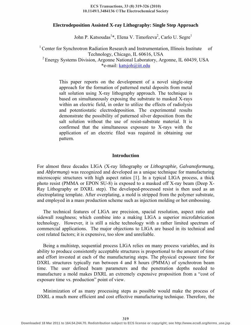
The experimental cell (fig.1), which was specifically designed for this experiment, consisted of two graphite plates sandwiched between three 25 mm thick Teflon plates (ASTMD 1710), each Teflon plate having a 75 mm circular window bored out to allow the incident X-ray beam to pass. The graphite plates (Goodfellow, 319-120-39) served as X-ray bulkhead windows for the cell, and as the working and counter electrodes of the three-electrode system. A silver-silver chloride (Ag/AgCl) electrode (BAS, MF-2052) was immersed into the cell volume from an orifice located at the top of the cell and used as a reference electrode. All the potentials reported in this paper are versus the potential of Ag/AgCl reference electrode (~0.235 V vs. SHE). An electrolyte solution (0.1 M AgNO3 in DI water) flowed into the cell from the bottom and removed from the top of the cell, and was circulated in a closed loop by a peristaltic pump (Masterflex, L/S by Cole-Palmer). The flow rate of solution was maintained between 100-300 ml/min. Electrodeposition was conducted in a potentiostatic regime at low overpotentials in order to provide a homogeneous growth of the deposits. An EZstat (NuVant Systems Inc.) potentiostat/galvanostat was used in all the experiments. The lithography mask was attached to the upstream face of the cell, and the entire assembly was scanned through the incident X-ray beam using an Aerotech UNIDEX 500 lithography scanner (machine resolution .0001 mm). The cell was scanned through the X-ray beam (size vert. 2 mm x hor. 62 mm) so as to avoid contact with the Teflon, and the scan rates ranged from 3.4 to 20 mm/sec. The main user selectable optical component employed during the exposures was an 879.50 mm long Pt coated mirror, essentially a low bandpass filter whose cutoff frequency was determined by the incident beam and mirror angle. The initial mirror angle was determined using two modeling programs (XOP 2.11 and Hephaestus) which accounted for all optically active components of the cell which were in line with the synchrotron beam and the position of the cell with respect to the beam source. The angle that was shown to have an X-ray absorption length of approximately 1 inch in a solution of 0.1 M AgNO3 was chosen.
ECS Transactions, 33 (8) 319-326 (2010)
320Downloaded 18 Mar 2011 to 164.54.244.70. Redistribution subject to ECS license or copyright; see http://www.ecsdl.org/terms_use.jsp
Figure 1. Experimental cell for simultaneous exposure to X-rays and electric field: R.E. – Ag/AgCl reference electrode; W.E. – working electrode; C.E. – counter electrode. The electrochemical system (two graphite electrodes in 0.1 M AgNO3 electrolyte with and Ag/AgCl reference electrode) was initially tested in the cyclic voltammetry (CV) regime. The cathodic potential window was expanded from an open circuit potential (OCP, 0.43 V vs. Ag/AgCl) with 50 mV steps (fig. 2). The Nernst equilibrium potential for silver deposition in 0.1 M AgNO3 solution (Ag+ + e- => Ag0) is at ~0.5 V vs. Ag/AgCl, however one can see form the CVs on figure 2 that significant current due to the onset of Ag phase formation is only observed at potentials below 0.43 V. To achieve noticeable deposition rates, while keeping nucleation rates under control, an electrodeposition potential of 0.35 V vs. Ag/AgCl was used for the majority of exposures, but higher overpotentials were tested as well.
ECS Transactions, 33 (8) 319-326 (2010)
321Downloaded 18 Mar 2011 to 164.54.244.70. Redistribution subject to ECS license or copyright; see http://www.ecsdl.org/terms_use.jsp

Figure 2. Cyclic voltammerty on carbon graphite electrode in 0.1 M AgNO3 solution. Cathodic potential was expanded 50 mV per each cycle.
Results and Discussion Irradiation of aqueous solution of metal ions leads to the radiolysis of water resulting in the formation of radicals, among which solvated electrons (e−aq) are strong reducing agents for the ions [2]. Their induced reduction leads to the formation of atoms, which aggregate and form metallic clusters. This technique has been successfully used in micro- and nano-fabrication either with γ-rays source [3-4], laser or electron beam [5] or more recently with X-rays [6-8]. Our approach to form metallic object of controlled size and shape relies on the combination of the radiolytic reduction of metal ions into atoms with the controlled potentiostatic deposition of metal from the solution. The electrodeposition potential is maintained at the value where the deposition rate is just slightly higher than the metal dissolution rate. The electrodeposition process denotes nucleation and growth of crystals under the influence of an electric field. Competition between growth and nucleation determines the granularity, structure and properties of the metallic deposits [9]. At low overpotentials the rate of nucleation is negligibly small and in the absence of growth sites the current is extremely slow. The hypothesis tested in the series of experiments is that simultaneous exposure to the masked off X-ray beam induces patterned nucleation sites through the radiolysis mechanisms [6] and controlled electrochemical growth of those nuclei produces the patterned metal deposit at the
ECS Transactions, 33 (8) 319-326 (2010)
322Downloaded 18 Mar 2011 to 164.54.244.70. Redistribution subject to ECS license or copyright; see http://www.ecsdl.org/terms_use.jsp
electrwhile
Figurdeposdurin FiAgNOthe msphercloseare owithi It radioelectrsolutispect
rode. This tee random nu
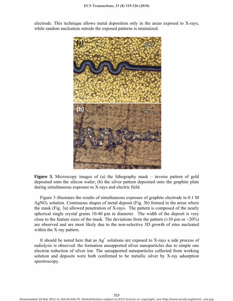
re 3. Microsited onto th
ng simultaneo
igure 3 illustO3 solution.
mask (Fig. 3arical single ce to the featuobserved andin the X-ray
should be nlysis is obseron reductioion and deptroscopy.
echnique allcleation outs
oscopy imaghe silicon wous exposur
trates the resContinuous
a) allowed pcrystal grain
ure sizes of thd are most lipattern.
noted here therved: the foon of silver posits were
lows metal side the expo
ges of (a) thwafer; (b) there to X-rays a
sults of simus shapes of mpenetration ons 10-40 μmhe mask. Thikely due to
hat as Ag+ sormation unsion. The unboth confir
deposition oosed pattern
he lithogrape silver patteand electric
ultaneous expmetal deposiof X-rays. Tm in diametehe deviationso the non-sel
olutions are supported si
nsupported nrmed to be
only in the ans is minimiz
phy mask –ern depositefield.
posure of grt (Fig. 3b) fo
The pattern ier. The wids from the plective 3D g
exposed to ilver nanopananoparticlesmetallic silv
areas exposezed.
inverse paed onto the g
raphite electrformed in thes composed
dth of the deattern (±10 μgrowth of si
X-rays a sidarticles due ts collected fver by X-ra
ed to X-ray
ttern of golgraphite plat
rode in 0.1 Me areas wherof the nearl
eposit is verμm or ~20%ites nucleate
de process oto simple onfrom workinay adsorptio
s,
ld te
M re ly ry
%) ed
of ne ng on
ECS Transactions, 33 (8) 319-326 (2010)
323Downloaded 18 Mar 2011 to 164.54.244.70. Redistribution subject to ECS license or copyright; see http://www.ecsdl.org/terms_use.jsp

Figure 4. (a) 3D topographical image of a deposit and (b) estimation of the aspect ratio from the profile. The topography of the deposits has been reconstructed using z-stack extended focus optical 3D imaging (Fig. 4a). In the image profile one can see (Fig. 4b) that the deposits have an approximate aspect ratio of 1:1 confirming the non-selective growth of nucleated sites. The 3D image shows the roughness of initial surface was quite high, indicating a wide range of surface energies - a potential obstacle towards obtaining homogeneous nucleation. Nevertheless, a continuous metallic pattern was formed on this surface. Using a more homogeneous electrode substrate may improve the quality and aspect ratio of the pattern. Besides surface roughness another avenue for improving aspect ratio is to create conditions for a selective growth in one crystal plane. Further work in this direction will allow this technique to establish itself as a competitive candidate for micro- and nanomanufacturing.
ECS Transactions, 33 (8) 319-326 (2010)
324Downloaded 18 Mar 2011 to 164.54.244.70. Redistribution subject to ECS license or copyright; see http://www.ecsdl.org/terms_use.jsp
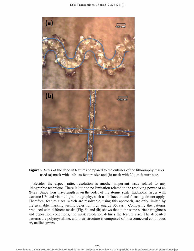
Figur
BelithogX-rayextremTherethe aproduand dpattercrysta
re 5. Sizes oused (a) m
esides the graphic techny. Since theime UV and efore, featuravailable mauced with dideposition crns are polycalline grains
of the deposimask with ~4
aspect rationique. Thereir wavelengtvisible light
re sizes, whiasking technifferent maskconditions, thcrystalline, as.
it features co40 μm featur
o, resolutioe is little to nth is on the t lithographyich are resonologies forks (Fig. 5a ahe mask resand their stru
ompared to thre size and (b
n is anothno limitationorder of they, such as dilvable, usin
r high energand 5b) showsolution defucture is com
he outlines ob) mask with
er importann related to te atomic scaliffraction ang this appro
gy X-rays. ws that at thefines the feamprised of in
of the lithogrh 20 μm fea
nt issue relthe resolvingle, traditiona
nd focusing, oach, are on
Comparinge same surfaature size. Tnterconnecte
raphy masksature size.
lated to ang power of aal issues witdo not apply
nly limited bg the patternace roughnesThe depositeed continuou
s
ny an th y.
by ns ss ed us
ECS Transactions, 33 (8) 319-326 (2010)
325Downloaded 18 Mar 2011 to 164.54.244.70. Redistribution subject to ECS license or copyright; see http://www.ecsdl.org/terms_use.jsp
Conclusions
In this paper we demonstrated the formation of a patterned silver deposit from salt solution on porous graphite plates, without the use of any resist-substrate material. The simultaneous exposure to X-rays with the application of an electric filed was required in obtaining our pattern. The silver deposits are polycrystalline continuous structures with less than 20% deviation from the mask features. These are due to a non-selective growth of nucleation centers formed in the X-ray path. The current aspect ratio is nearly 1:1, but could be significantly improved by using a more homogeneous electrode surface and controlling the selective growth in one crystal plane. A side reaction of this entire process is formation of unsupported silver nanoparticles due to radiolysis.
Acknowledgements
We thank Ralu Divan for her guidance and help and Jeremy Kropft for his critical opinion on design and the concept of the experiments. We appreciate MRCAT for the presented opportunity and support of lithography program throughout the years. Aknowlegements to technical support and cooperation from NuVant Inc. provided us with equipment for electrochemical part of the experiment. Many thanks to Nicholas Andrisevic and Brad Etter from Carl Zeiss Inc. for help with 3D topography of the samples.
References
(1) V. Saile, U. Wallrabe, O. Tabata, J.G. Korvink, Eds., LIGA and Its Applications, Vol. 7., Wiley-VCH: Weinheim, Germany (2009).
(2) G.V. Buxton, R.M. Sellers, Coordination Chemistry Reviews, 22, 195 (1977). (3) D.B. Yu, X.Q. Sun, J.T. Bian, Z.C. Tong, Y.T. Qian, Physica E-Low-Dimensional
Systems & Nanostructures, 23, 50 (2004). (4) H. Remita, I. Lampre, M. Mostafavi, E. Balanzat, S. Bouffard, Radiation Physics
and Chemistry, 72, 575 (2005). (5) F. Stellacci, C.A. Bauer, T. Meyer-Friedrichsen, W. Wenseleers, V. Alain, S.M.
Kuebler, S. J. K. Pond, Y. D. Zhang, S. R.Marder, J. W. Perry, Advanced Materials, 14, 194 (2002).
(6) R. Divan, D.C. Mancini, N. Moldovan, L. Assoufid, Y.S. Chu, Q. Ma, R.A. Rosenberg, 2003 International Semiconductor Conference, Proceedings Vols 1 and 2, p. 39, (2003).
(7) Q. Ma, R. Divan, D.C. Mancini, R.A. Rosenberg, J.P. Quintana, D.T. Keane, Applied Physics Letters, 89, 83114 (2006).
(8) M.F. Bertino, R.R. Gadipalli, L.A. Martin, L.E. Rich, A.Yamilov, B.R. Heckman, N. Leventis, S. Guha, J. Katsoudas, R. Divan, D.C. Mancini, Nanotechnology, 18, 315603 (2007).
(9) E. Budevski, G. Staikov, W.J. Lorenz, Electrochemical Phase Formation and Growth. An introduction to the Initial Stages of Metal Deposition, VCH Verlagsgesellschaft mbH: Weinheim, Germany (1996).
ECS Transactions, 33 (8) 319-326 (2010)
326Downloaded 18 Mar 2011 to 164.54.244.70. Redistribution subject to ECS license or copyright; see http://www.ecsdl.org/terms_use.jsp


