Embed Size (px)
Citation preview
Large Area, Facile Oxide Nanofabrication via Step-and-Flash ImprintLithography of Metal−Organic Hybrid ResinsSaman Safari Dinachali,†,‡ Jarrett Dumond,*,† Mohammad S. M. Saifullah,*,†
Kwadwo Konadu Ansah-Antwi,†,§ Ramakrishnan Ganesan,∥ Eng San Thian,‡ and Chaobin He†,⊥
†Institute of Materials Research and Engineering, A*STAR (Agency for Science, Technology and Research), 3 Research Link,Singapore 117602, Republic of Singapore‡Department of Mechanical Engineering, National University of Singapore, 9 Engineering Drive 1, Singapore 117576, Republic ofSingapore§Department of Electrical and Computer Engineering, National University of Singapore, E4-5-45, 4 Engineering Drive 3, Singapore117583, Republic of Singapore∥Department of Chemistry, Birla Institute of Technology & Science, Pilani−Hyderabad Campus, Jawahar Nagar, Shameerpet Mandal,Hyderabad 500 078, Andhra Pradesh, India⊥Department of Materials Science & Engineering, National University of Singapore, 21 Lower Kent Ridge Road, Singapore 119077,Republic of Singapore
*S Supporting Information
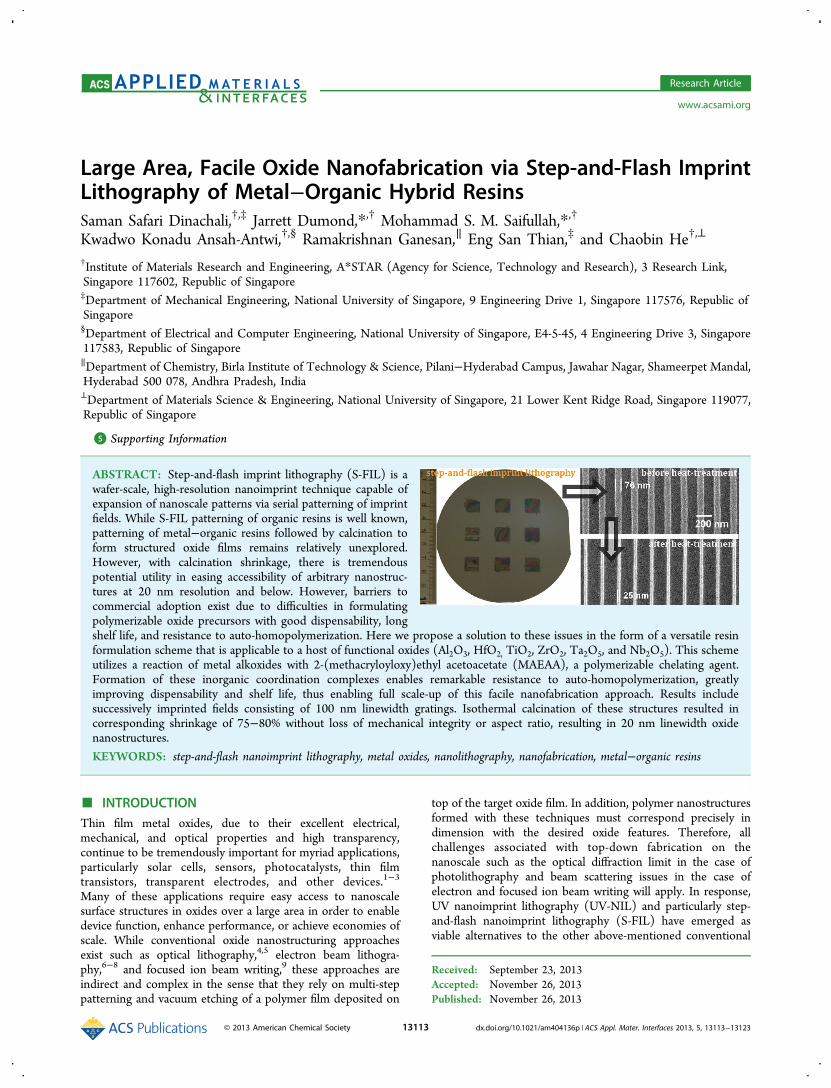
ABSTRACT: Step-and-flash imprint lithography (S-FIL) is awafer-scale, high-resolution nanoimprint technique capable ofexpansion of nanoscale patterns via serial patterning of imprintfields. While S-FIL patterning of organic resins is well known,patterning of metal−organic resins followed by calcination toform structured oxide films remains relatively unexplored.However, with calcination shrinkage, there is tremendouspotential utility in easing accessibility of arbitrary nanostruc-tures at 20 nm resolution and below. However, barriers tocommercial adoption exist due to difficulties in formulatingpolymerizable oxide precursors with good dispensability, longshelf life, and resistance to auto-homopolymerization. Here we propose a solution to these issues in the form of a versatile resinformulation scheme that is applicable to a host of functional oxides (Al2O3, HfO2, TiO2, ZrO2, Ta2O5, and Nb2O5). This schemeutilizes a reaction of metal alkoxides with 2-(methacryloyloxy)ethyl acetoacetate (MAEAA), a polymerizable chelating agent.Formation of these inorganic coordination complexes enables remarkable resistance to auto-homopolymerization, greatlyimproving dispensability and shelf life, thus enabling full scale-up of this facile nanofabrication approach. Results includesuccessively imprinted fields consisting of 100 nm linewidth gratings. Isothermal calcination of these structures resulted incorresponding shrinkage of 75−80% without loss of mechanical integrity or aspect ratio, resulting in 20 nm linewidth oxidenanostructures.
KEYWORDS: step-and-flash nanoimprint lithography, metal oxides, nanolithography, nanofabrication, metal−organic resins
■ INTRODUCTIONThin film metal oxides, due to their excellent electrical,mechanical, and optical properties and high transparency,continue to be tremendously important for myriad applications,particularly solar cells, sensors, photocatalysts, thin filmtransistors, transparent electrodes, and other devices.1−3
Many of these applications require easy access to nanoscalesurface structures in oxides over a large area in order to enabledevice function, enhance performance, or achieve economies ofscale. While conventional oxide nanostructuring approachesexist such as optical lithography,4,5 electron beam lithogra-phy,6−8 and focused ion beam writing,9 these approaches areindirect and complex in the sense that they rely on multi-steppatterning and vacuum etching of a polymer film deposited on
top of the target oxide film. In addition, polymer nanostructuresformed with these techniques must correspond precisely indimension with the desired oxide features. Therefore, allchallenges associated with top-down fabrication on thenanoscale such as the optical diffraction limit in the case ofphotolithography and beam scattering issues in the case ofelectron and focused ion beam writing will apply. In response,UV nanoimprint lithography (UV-NIL) and particularly step-and-flash nanoimprint lithography (S-FIL) have emerged asviable alternatives to the other above-mentioned conventional
Received: September 23, 2013Accepted: November 26, 2013Published: November 26, 2013
Research Article
www.acsami.org
© 2013 American Chemical Society 13113 dx.doi.org/10.1021/am404136p | ACS Appl. Mater. Interfaces 2013, 5, 13113−13123
techniques due to their ability to access the nanoscale withoutthe light diffraction and beam scattering limitations notedabove. In addition, these contact lithography approaches retaina favorable combination of simplicity, versatility, low cost, andthe potential for achieving high throughput.10−14 Unfortu-nately, mold templates used in UV-NIL and S-FIL generallyrely upon the above-mentioned conventional lithographytechniques for fabrication. Thus, indirectly, the same lightdiffraction and beam scattering limitations apply to nano-imprinting techniques through mold fabrication as is applicableto conventional lithography. One way of lifting theselimitations, in addition to enabling a unique means ofnanostructuring oxide films, is to take advantage of thecalcination shrinkage inherent to sol−gel processing to easilyaccess the nanoscale from much larger patterned features. Forexample, it is possible to form 100 nm diameter hybrid metal−organic structures and, with calcination shrinkage, achieve 20nm equivalent oxide structures of the same aspect ratio, featuredensity, and pitch. Note that the duty cycle, or surface areacoverage of features, is reduced by calcination shrinkage. Thiscan, to a certain extent, be compensated for by increasing theduty cycle of the as-imprinted metal−organic structures and bytuning the degree of calcination shrinkage such that the amountof shrinkage required to achieve the desired resolution in oxideis minimized. However, care must be taken to select end-applications that do not require extremely high densitynanostructures for use with this approach.In any case, by adapting metal−organic materials for use in S-
FIL, it is possible to fabricate mold templates with features upto 8 times larger in diameter than the actual desired structures.Such a feat would significantly improve the ease and economicsof fabrication, as S-FIL can then be used to expand the coveragearea of the calcined oxide nanostructures in step-and-repeatfashion.In recent years, the importance of organic−inorganic hybrid
resins to fabricate nanostructures with inorganic character usingNIL has gained considerable attention.15−23 However, conven-tional NIL techniques such as UV and thermal NIL rely heavilyon a one-step, whole-wafer patterning process, which requires alarge and expensive mold to achieve large area patterning.Furthermore, the difficulty in controlling and minimizingdefects and achieving good residual layer uniformity increasesconsiderably with increasing imprint field area. S-FIL incontrast can utilize relatively small molds in order to solveboth issues of economics and defect control. Furthermore, S-FIL is greatly advantaged over competing nanoimprintingtechniques by its employment of drop-on-demand inkjetdispensing in order to fill non-uniform mold cavity distributionswhile retaining uniform residual layer thicknesses. In additionto easier access to the nanoscale via calcination, S-FILfabrication with hybrid resins exhibits a number of otheradvantages over other oxide patterning techniques. Theseinclude a general reduction in the number of steps involved insurface structuring and device fabrication, lower overall processtemperatures relative to direct melt embossing of oxides, andcomplete elimination of the need for vacuum etching forapplications that do not require etching of the substrate.A persisting challenge in developing metal−organic resins for
S-FIL has been their consistently poor dispensability and lowshelf life due to their susceptibility to auto-homopolymeriza-tion.16,24 S-FIL is generally achieved by pressing a rigid,patterned template or mold into a UV-curable liquid resin toform a corresponding pattern in the resin film. Subsequently,
the formed film is cured with an ultraviolet light to enable thereverse tone transfer of the mold topography into the film upondemolding. The resin is typically deposited using an inkjetdispensing unit, which is subject to clogging if the resinviscosity increases by only a few millipascal-seconds. Withmetal−organic hybrid resins, clogging issues are a severechallenge because auto-homopolymerization can easily generatesuch an increase in the resin viscosity. Thus, the resin shelf lifecan be as short as 2 or 3 days. More importantly, because theresin viscosity strongly influences the actual dispense volume,this instability makes it extremely difficult to achievereproducible and predictable fabrication results in terms offilm and residual layer thicknesses, control of field uniformity,and avoidance of an under-filling condition. In terms of scale-upto commercialization and large-scale expansion of nanostruc-tures, a solution to these difficulties is crucial.A potential solution to the problem of obtaining a more
chemically stable oxide precursor was recently proposed byDinachali et al. by reacting metal alkoxides with a polymerizablechelating agent such as 2-(methacryloyloxy)ethyl acetoacetate(MAEAA).15 MAEAA possesses β-ketoester and methacrylategroupsthe former leads to the formation of highly stable,chelated alkoxide complexes, while the latter provides thereactive group for participation in free-radical polymerization.The reaction of a metal alkoxide with MAEAA results in theformation of a metal−organic precursor mixed with an alcoholbyproduct. Preliminary assessment of the suitability of theseprecursors was carried out by removing the alcohol byproductunder reduced pressure followed by examination to check forauto-homopolymerization. The resultant product was a stable,transparent, lightly colored, polymerizable, and viscous liquidmetal oxide precursor freely soluble in acrylate-based reactivediluents with remarkable immunity to auto-homopolymeriza-tion. Resins formulated using these chelated oxide precursorsexhibited at least a 30-fold improvement in shelf life relative topreviously reported formulation schemes.24 Along withenhanced performance and shelf life, in this work, we haveutilized the aforementioned improved resin formulationapproach to demonstrate a versatile approach for S-FILpatterning of a host of metal oxides such as Al2O3, HfO2,TiO2, ZrO2, Nb2O5, and Ta2O5 in step-and-repeat fashion overlarge areas. Although patterned examples of all the oxides willbe given, Nb2O5 in particular will be used as a representativecandidate for discussing resin behavior.
■ RESULTS AND DISCUSSIONIn general, liquid resins possess good transport properties toenable faster filling of mold cavities and the spreading of resinfrom areas where feature density is low to other regions wherefeature density is higher at low pressure (∼100 kPa). S-FILexploits these advantages in the fabrication of micro- andnanostructures in step-and-repeat fashion over an entire waferat speeds in excess of, or competitive with, conventionaltechniques such as photolithography and electron beamwriting, respectively. In S-FIL, a low-viscosity, photo-curableresin is locally dispensed dropwise on the substrate over a dropmap area corresponding to the template patterned area. Then, aquartz template is brought into contact with the resin to form astack. The resin is then photo-polymerized by exposing it toUV light through the transparent template, resulting in theformation of rigid imprinted features. In terms of fully organicresins, the photo-polymerizable monomers used in S-FIL aretypically either acrylate- or vinyl ether-based formulations, with
ACS Applied Materials & Interfaces Research Article
dx.doi.org/10.1021/am404136p | ACS Appl. Mater. Interfaces 2013, 5, 13113−1312313114

the former more popular than the latter due to easy availabilityof inexpensive monomers.25−29
Most scientific activity in the field is largely confined tothermally curable resin formulations, as the monomer andprecursor synthesis is relatively straightforward, and processingdoes not place significant restrictions on the resin properties.However, for successful S-FIL patterning of metal−organicresins, the precursor must be transparent, stable, fast curing,and of low enough viscosity to be inkjet dispensable.Furthermore, organic solvent in the resin must be kept tonear-zero, as evaporation at an inkjet dispense orifice leads tocondensation at the tip and this causes the alkoxide toprecipitate out, leading to a white residue build-up that clogsthe dispense tip orifice. These stringent requirements makemetal−organic hybrid resin development for S-FIL a significantchallenge.The success of patterning functional metal oxides using S-
FIL strongly depends on the resin formulation. Broadlyspeaking, there are four main components. First, a polymer-izable metal oxide precursor, usually an inorganic coordinationcomplex, which participates in polymerization during UVexposure and forms metal oxide after calcination of theimprinted structures. Second, a reactive diluent that is used toadjust the viscosity of the polymerizable metal−organiccomplex. Third, a cross-linker which provides mechanicalstrength, and finally fourth, a photo-initiator to initiate photo-polymerization leading to solidification of the resin. Amongthese four, the most critical component of the resin is thepolymerizable metal oxide precursor. Such a complex shouldpreferably be of low viscosity, transparent, resistant to auto-homopolymerization, and stable against hydrolytic activity. Apopular way to form polymerizable metal−organic complexes isto react a metal alkoxide with a polymerizable monomer such asmethacrylic acid or 3-butenoic acid.16,24 This is because of thesimplicity of the reaction, as metal alkoxides are very reactivecompounds due to the presence of electronegative alkoxygroups that cause the metal atom to be highly prone tonucleophilic attack. Unfortunately, in most cases, the reactionbetween metal alkoxides with methacrylic acid16 or 3-butenoicacid24 does not yield a processable liquid. Furthermore, metalmethacrylates, and to some extent allyl-functionalized metalcomplexes, suffer from a shorter shelf life due to the problem ofauto-homopolymerization. Therefore, an improved reactionscheme for S-FIL resin formulation is desirable.It has recently been reported that reacting metal alkoxides
with a polymerizable chelating agent such as MAEAA yields apolymerizable metal−organic liquid that is clear, stable,flowable, and of low viscosity.15 MAEAA is a bi-functionalmolecule that possesses β-ketoester and methacrylate groups.The β-ketoester group is capable of undergoing keto−enoltautomerism, as shown in eq 1; the enol form of MAEAA isstabilized by chelation with tantalum ethoxide that results in theformation of a chemically stable, chelated alkoxide perhaps dueto steric hindrance (eq 2). In sol−gel chemistry, it is well-known that β-ketoester- and β-diketone-based chelating agentsstabilize alkoxides and increase their long-term resistanceagainst hydrolysis. This technique has been effectively utilizedto pattern oxides using photolithography,4,5 electron beamlithography,6,7 two-photon lithography,30 direct write assem-bly,31 electrohydrodynamic lithography,32 and proton beamwriting.33 In our case, the key to achieving long-term hydrolyticstability of our oxide precursors is the stabilization of alkoxidesusing a β-ketoester such as MAEAA, a chelating agent. We have
used MAEAA because it possesses β-ketoester and methacrylategroupsthe former leads to the formation of highly stable,chelated alkoxide complexes, while the latter provides a reactivemonomer that takes part in polymerization in the presence of aphoto-initiator. The chelating reaction often results in a slightcolor change of the solution and yields a polymerizable metal−organic precursor.The key condition that enables compatibility with S-FIL is in
the selection of state for the candidate metal alkoxide. Onlyliquid-state metal alkoxides have sufficiently low viscosity atroom temperature to achieve formulated resin viscosities below20 mPa·s, the latter being an important threshold viscosity forinkjet dispensing.27 This condition was not reported in priorworks where both liquid and solid-state metal alkoxides wereemployed without distinction. One challenge that may arisegiven the state requirement would be cases where solid metalalkoxides are required as feedstock, or is the only available statefor a given metal alkoxide. Further research into the feasibilityof heating the metal−organic resin during inkjet dispensewould be required in order to lower the viscosity to below thedispense threshold.A further important development in enabling S-FIL
processing was the elimination of organic solvents. This iscontrary to common practice with purely organic resins wheresuch solvents are used extensively for cleaning of the inkjetdispense line and dispense tip. Cleaning of our metal−organicresins leads to deposition of alkoxide residues at the tip orificeand along the dispense line upon evaporation of the solvent,leading to extensive clogging. Additionally, alcohols willgenerally cause the alkoxide components to precipitate out ofthe resin, presumably due to alcoholysis,34 forming insolubleparticles that will clog the inkjet dispense unit long afterremoval of the metal−organic resin. Thus, solvents were notused for cleaning the inkjet dispense unit, aside from thedispense tips which were cleaned with multiple solvents toremove all residues prior to thorough drying. This approachenabled full, automated step-and-repeat imprinting withoutclogging issues.Preliminary studies were conducted to study the suitability of
liquid-state metal alkoxides for S-FIL resin formulation. First,
ACS Applied Materials & Interfaces Research Article
dx.doi.org/10.1021/am404136p | ACS Appl. Mater. Interfaces 2013, 5, 13113−1312313115
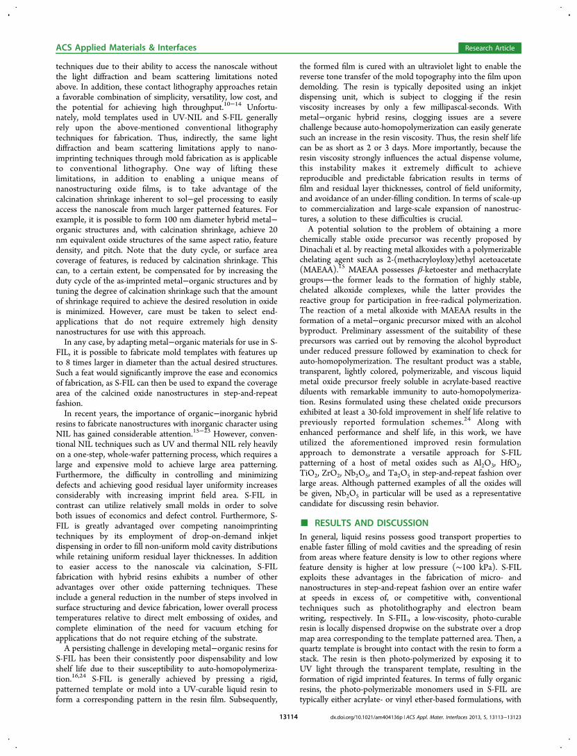
various chelated metal alkoxides (of Al, Hf, Ti, Zr, Nb, and Ta)were subjected to a low pressure environment so as to removethe alcohol byproduct (eq 3). Removal of alcohol byproductstypically led to the formation of transparent, often slightlycolored liquids containing polymerizable oxide precursors thatwere remarkably resistant to auto-homopolymerization (Figure1a). We speculate two-fold reasons for the exceptional stabilityof metal alkoxides chelated with MAEAA in comparison totheir corresponding methacrylic acid- and allyl-terminatedcarboxylic acid-chelated derivatives. Firstly, the very nature ofthe chelation between the metal center and the ligands isdifferent. In the case of a carboxylic acid, the carboxylate anionreplaces the alkoxy group and binds to the metal center andthus results in the final product having the same co-ordinationnumber as the alkoxide. By contrast, when MAEAA (a β-
ketoester in its enol form) is substituted for an alkoxy group, itresults in the final product having an additional co-ordinationnumber due to the extra co-ordination bond between the β-ketoester group and the metal center. Secondly, the chemicalenvironment of the reactive end group may be reducing theoccurrence of auto-homopolymerization. The longer chainlength of MAEAA molecules further separates the methacrylategroups from each other due to steric hindrance. As a result, thenumber of collisions between the methacrylate groups isreduced, thereby decreasing the probability of auto-homo-polymerization. This is in striking contrast to metalmethacrylates (and to some extent allyl-functionalized metalcomplexes), as they undergo auto-homopolymerization uponany attempt to remove alcohol present as a byproduct from thereaction of a metal alkoxide with methacrylic acid.16,24 We
Figure 1. (a) Clear, stable, and slightly colored metal oxide precursors formed when alcohol byproduct was removed following the reaction shown ineq 3. (b) Characteristic infrared absorption peaks of metal oxide precursors formed by reacting metal alkoxide and MAEAA in a 1:2 ratio. The broadvibration bands corresponding to particular bonds are indicated at the top. Table 1 shows details of the band assignment.
ACS Applied Materials & Interfaces Research Article
dx.doi.org/10.1021/am404136p | ACS Appl. Mater. Interfaces 2013, 5, 13113−1312313116
believe that these synergistic factors contribute to the enhancedshelf life of the MAEAA-chelated metal precursors. Predictably,all the chelated precursors, except for ZrO2, showed excellentstability over a storage period of more than 3 months at roomtemperature. They were found to be transparent and flowable.The storage period for ZrO2 was found to be limited to ∼2weeks.
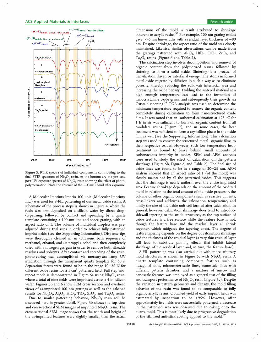
To understand the chelation reaction, FTIR spectroscopywas used to characterize the viscous polymerizable metal oxideprecursors (Figure 1b). Their FTIR spectra were found to besimilar and show a large number of absorption bands/peaksbetween 1000 and 1800 cm‑1. The pair of absorption peakscorresponding to the ν( ‐‐‐
C C) and ν( ‐‐‐C O) vibrations of the
chelate ring at 1522 and 1609 cm−1, respectively, is attributedto the bidentate character of cation-bonded MAEAA. This isindicative of the formation of the chelated complex.35,36
Noteworthy is the presence of characteristic peaks of thecarbonyl group at 1721 cm−1 and the methacrylate double bondat 1634 cm−1 in MAEAA-functionalized metal oxide precursors;the latter strongly suggests the preservation of a polymerizabledouble bond in the complex. A shoulder at 1746 cm‑1 thatcorresponds to the carbonyl group of MAEAA may indicateincomplete reaction between MAEAA and the correspondingmetal alkoxides (Figure 1b).36
Resins for the S-FIL of oxides were formulated by addingreactive diluent, cross-linker, and photo-initiator to therespective polymerizable metal oxide precursors. Since theprecursors have a relatively high viscosity, iso-butyl acrylate, areactive diluent, was added to lower the viscosity. Ethyleneglycol diacrylate served as a cross-linker, and due to its relativelylow viscosity, it also partly served the purpose of a reactivediluent. The molar ratio between alkoxide, MAEAA, iso-butylacrylate, and ethylene glycol diacrylate was 1:2:2:1 for Al2O3,HfO2, TiO2, and ZrO2 resins. On the other hand, Ta2O5 andNb2O5 resins had a ratio of 1:2:1:1. Additional iso-butyl acrylatewas added to the former set of resins due to the relatively highviscosity of their oxide precursors. Of course, it is worthwhile tonote that reducing the viscosity in this manner comes at thecost of additional shrinkage and loss of oxide content uponcalcination. The formulation of the above-mentioned molarratios takes this consideration into mind in order to maintainpost-calcination integrity. The final resin composition in allcases possessed a viscosity of <10 mPa·s. For comparison,Nb2O5 resin and a fully organic “blank” formulation in a 2:1:1molar ratio of MAEAA, iso-butyl acrylate, and ethylene glycoldiacrylate exhibited viscosities of 7.5 and 4.6 mPa·s,respectively. These resin formulations were found to possessexcellent dispensability with viscosities well within thesuggested limit of 20 mPa·s.27
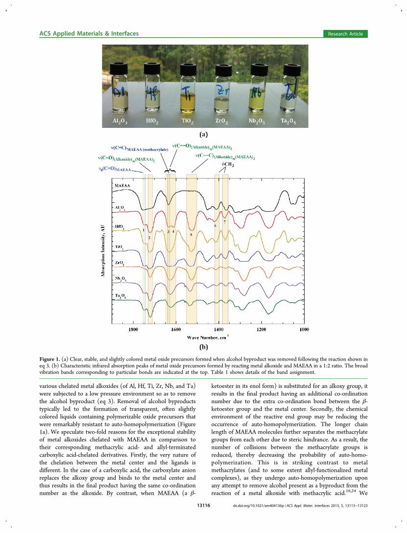
To determine the absorbance of UV radiation by the oxideresins, ultraviolet-visible (UV-vis) spectrophotometry wascarried out (Figure 2a). It was seen that Al2O3, HfO2, ZrO2,
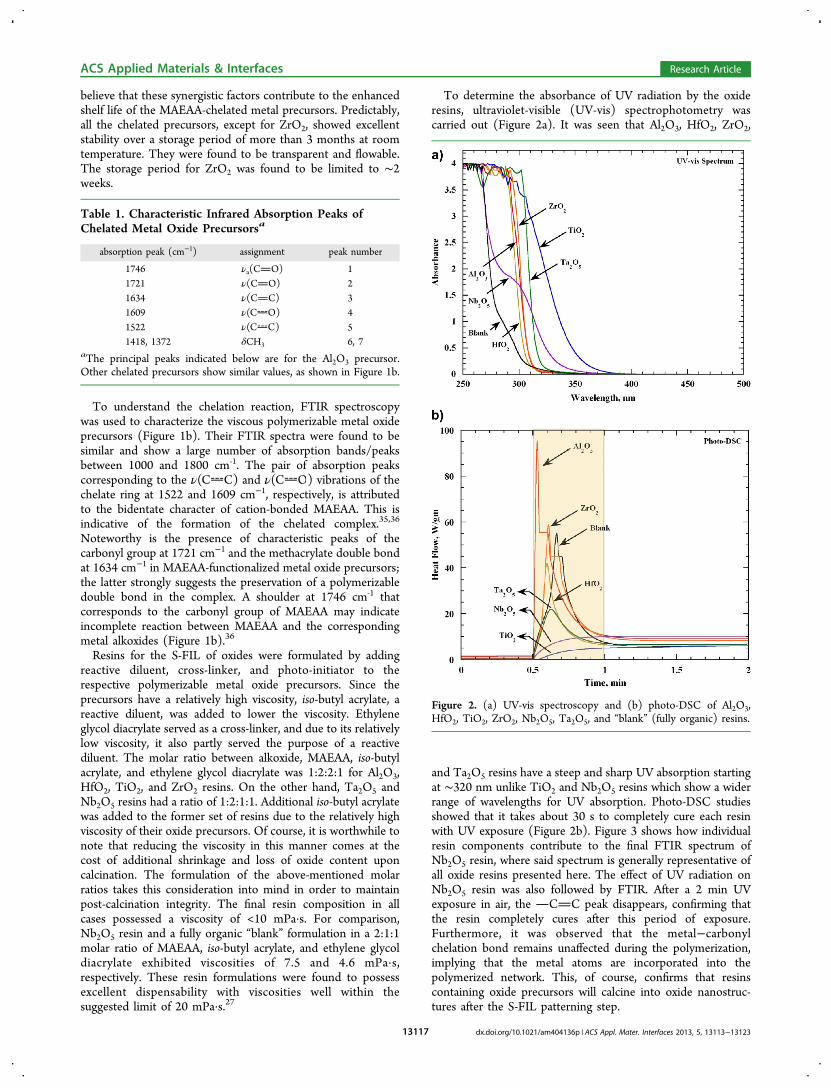
and Ta2O5 resins have a steep and sharp UV absorption startingat ∼320 nm unlike TiO2 and Nb2O5 resins which show a widerrange of wavelengths for UV absorption. Photo-DSC studiesshowed that it takes about 30 s to completely cure each resinwith UV exposure (Figure 2b). Figure 3 shows how individualresin components contribute to the final FTIR spectrum ofNb2O5 resin, where said spectrum is generally representative ofall oxide resins presented here. The effect of UV radiation onNb2O5 resin was also followed by FTIR. After a 2 min UVexposure in air, the CC peak disappears, confirming thatthe resin completely cures after this period of exposure.Furthermore, it was observed that the metal−carbonylchelation bond remains unaffected during the polymerization,implying that the metal atoms are incorporated into thepolymerized network. This, of course, confirms that resinscontaining oxide precursors will calcine into oxide nanostruc-tures after the S-FIL patterning step.
Table 1. Characteristic Infrared Absorption Peaks ofChelated Metal Oxide Precursorsa
absorption peak (cm−1) assignment peak number
1746 νa(CO) 11721 ν(CO) 21634 ν(CC) 31609 ν( ‐‐‐
C O) 41522 ν( ‐‐‐
C C) 51418, 1372 δCH3 6, 7
aThe principal peaks indicated below are for the Al2O3 precursor.Other chelated precursors show similar values, as shown in Figure 1b.
Figure 2. (a) UV-vis spectroscopy and (b) photo-DSC of Al2O3,HfO2, TiO2, ZrO2, Nb2O5, Ta2O5, and “blank” (fully organic) resins.
ACS Applied Materials & Interfaces Research Article
dx.doi.org/10.1021/am404136p | ACS Appl. Mater. Interfaces 2013, 5, 13113−1312313117
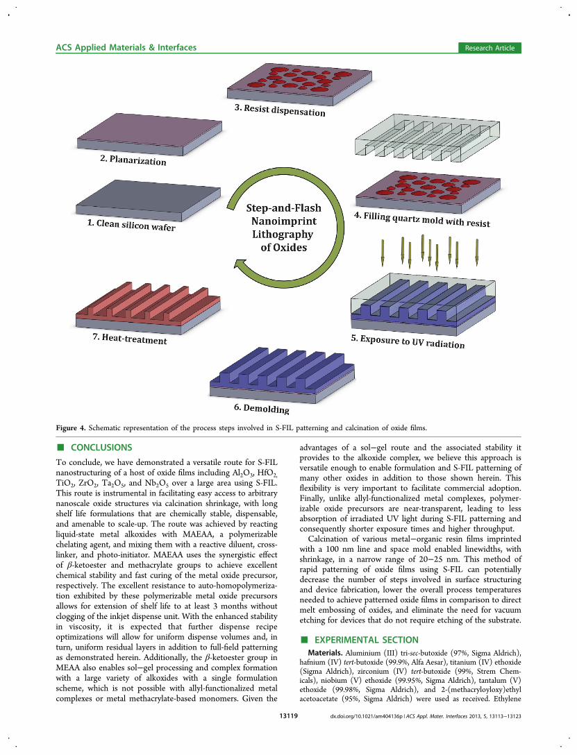
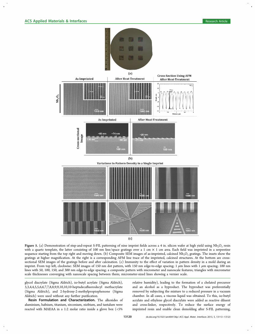
A Molecular Imprints Imprio 100 unit (Molecular Imprints,Inc.) was used for S-FIL patterning of our metal oxide resins. Aschematic of the process steps is shown in Figure 4, where theresin was first deposited on a silicon wafer by direct drop-dispensing, followed by contact and spreading by a quartztemplate containing a 100 nm line and space grating, with anaspect ratio of 1. The volume of individual droplets was pre-adjusted during trial runs in order to achieve fully patternedimprint fields (see the Supporting Information). Dispense tipswere thoroughly cleaned in an ultrasonic bath sequence ofmethanol, ethanol, and iso-propyl alcohol and then completelydried with a nitrogen gas gun in order to remove both alkoxideresidues and solvents. After contact and spreading of the resin,photo-curing was accomplished via mercury-arc lamp UVirradiation through the transparent quartz template for 60 s.Separation forces were found to be in the range 10−25 N fordifferent oxide resins for a 1 cm2 patterned field. Full step-and-repeat mode is demonstrated in Figure 5a using Nb2O5 resin,where a total of nine fields were imprinted across a 4 in. siliconwafer. Figures 5b and 6 show SEM cross section and overheadviews of as-imprinted 100 nm gratings as well as the calcinedresults for Nb2O5, Al2O3, HfO2, TiO2, ZrO2, and Ta2O5 resins.Due to similar patterning behavior, Nb2O5 resin will be
discussed here in greater detail. Figure 5b shows the top viewand cross-sectional SEM images of imprinted Nb2O5 resin. Thecross-sectional SEM image shows that the width and height ofthe as-imprinted features were slightly smaller than the actual
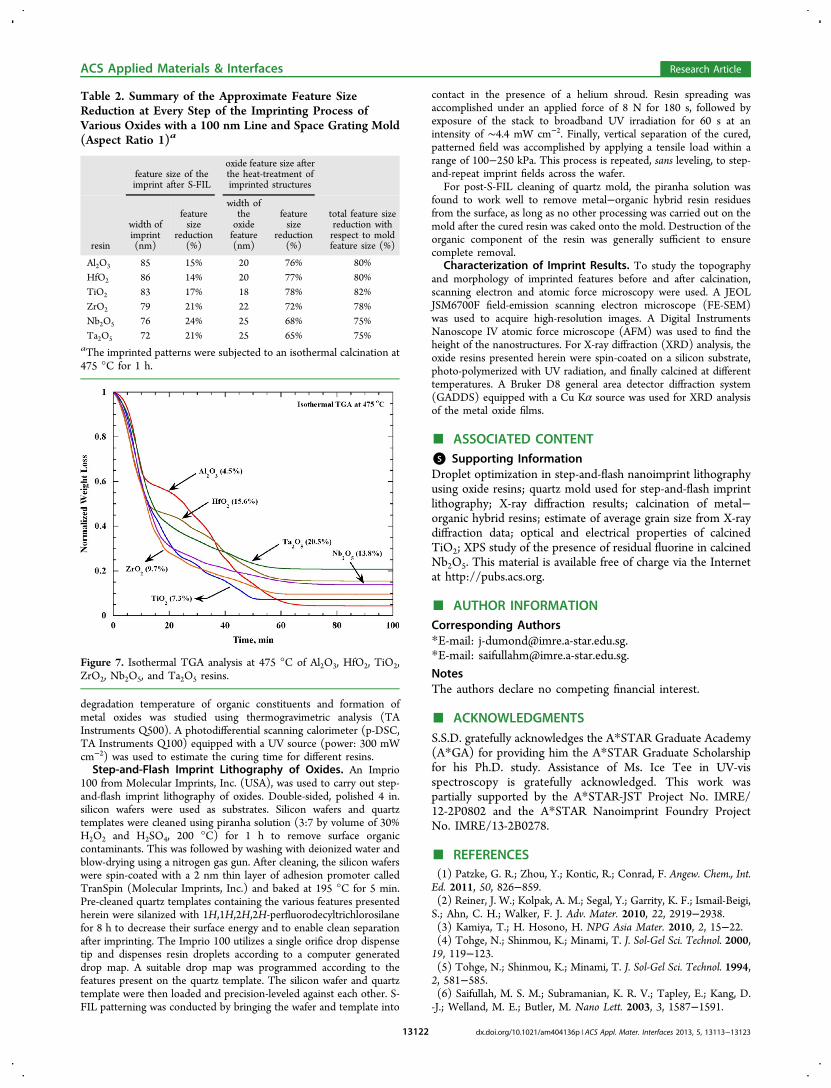
dimensions of the mold, a result attributed to shrinkageinherent to acrylic resins.37 For example, 100 nm grating moldsgave ∼76 nm line-widths with a residual layer thickness of ∼80nm. Despite shrinkage, the aspect ratio of the mold was closelymaintained. Likewise, similar observations can be made fromthe gratings patterned with Al2O3, HfO2, TiO2, ZrO2, andTa2O5 resins (Figure 6 and Table 2).The calcination step involves decomposition and removal of
organic content from the polymerized resins, followed bysintering to form a solid oxide. Sintering is a process ofdensification driven by interfacial energy. The atoms in formedmetal-oxide migrate by diffusion in such a way as to eliminateporosity, thereby reducing the solid−air interfacial area andincreasing the oxide density. Holding the sintered material at ahigh enough temperature can lead to the formation ofnanocrystalline oxide grains and subsequently their growth viaOstwald ripening.38 TGA analysis was used to determine theminimum temperature required to remove the organic contentcompletely during calcination to form nanostructured oxidefilms. It was noted that an isothermal calcination at 475 °C for1 h in air was sufficient to burn off organic content from allcandidate resins (Figure 7), and in some cases, the heattreatment was sufficient to form a crystalline phase in the oxidefilm as well (see the Supporting Information). This calcinationstep was used to convert the structured metal−organic films totheir respective oxides. However, such low temperature heat-treatment is bound to leave behind small amounts ofcarbonaceous impurity in oxides. SEM and AFM analyseswere used to study the effect of calcination on the patternshrinkage (Figure 5b, Figure 6, and Table 2). The final size ofoxide lines was found to be in a range of 20−25 nm. AFManalysis showed that an aspect ratio of 1 (of the mold) wasclosely maintained by all the patterned oxides. This suggeststhat the shrinkage is nearly uniform over the entire imprintedarea. Feature shrinkage depends on the amount of the oxidizedmetal in relation to the total amount of the oxide precursor, thevolume of other organic components such as reactive diluents,cross-linkers and additives, the calcination temperature, andfinally the size of the oxide unit cell formed after calcination. Ingeneral, however, calcination shrinkage does tend to introducesidewall tapering to the oxide structures, as the top surface ofoxide features is a free surface while the feature base is not,though the feature base and the residual layer all shrinktogether, which mitigates the tapering effect. The degree offeature tapering depends on the degree of calcination shrinkageand the thickness of the residual layer (a very thin residual layerwill lead to substrate pinning effects that inhibit lateralshrinkage of the residual layer and, in turn, the feature base).S-FIL patterning was also carried out with more arbitrary
mold structures, as shown in Figure 5c with Nb2O5 resin. Aquartz template containing composite features such ashexagonal dots, micrometer-scale lines, nanoscale lines withdifferent pattern densities, and a mixture of micro- andnanoscale features was employed as a general test of the fillingand transport performance of Nb2O5 resin (Figure 5c). Despitethe variation in pattern geometry and density, the mold fillingbehavior of the resin was found to be comparable to fullyorganic acrylic resins. Obtained yield of early imprint fields wasestimated by inspection to be >95%. However, afterapproximately five fields were successfully patterned, a decreasein the patterned area was observed due to caking onto thequartz mold. This is most likely due to progressive degradationof the silanized anti-stick coating applied to the mold.39
Figure 3. FTIR spectra of individual components contributing to thefinal FTIR spectrum of Nb2O5 resin. At the bottom are the pre- andpost-UV exposure spectra of Nb2O5 resin showing the effect of photo-polymerization. Note the absence of the CC band after exposure.
ACS Applied Materials & Interfaces Research Article
dx.doi.org/10.1021/am404136p | ACS Appl. Mater. Interfaces 2013, 5, 13113−1312313118
■ CONCLUSIONS
To conclude, we have demonstrated a versatile route for S-FILnanostructuring of a host of oxide films including Al2O3, HfO2,TiO2, ZrO2, Ta2O5, and Nb2O5 over a large area using S-FIL.This route is instrumental in facilitating easy access to arbitrarynanoscale oxide structures via calcination shrinkage, with longshelf life formulations that are chemically stable, dispensable,and amenable to scale-up. The route was achieved by reactingliquid-state metal alkoxides with MAEAA, a polymerizablechelating agent, and mixing them with a reactive diluent, cross-linker, and photo-initiator. MAEAA uses the synergistic effectof β-ketoester and methacrylate groups to achieve excellentchemical stability and fast curing of the metal oxide precursor,respectively. The excellent resistance to auto-homopolymeriza-tion exhibited by these polymerizable metal oxide precursorsallows for extension of shelf life to at least 3 months withoutclogging of the inkjet dispense unit. With the enhanced stabilityin viscosity, it is expected that further dispense recipeoptimizations will allow for uniform dispense volumes and, inturn, uniform residual layers in addition to full-field patterningas demonstrated herein. Additionally, the β-ketoester group inMEAA also enables sol−gel processing and complex formationwith a large variety of alkoxides with a single formulationscheme, which is not possible with allyl-functionalized metalcomplexes or metal methacrylate-based monomers. Given the
advantages of a sol−gel route and the associated stability itprovides to the alkoxide complex, we believe this approach isversatile enough to enable formulation and S-FIL patterning ofmany other oxides in addition to those shown herein. Thisflexibility is very important to facilitate commercial adoption.Finally, unlike allyl-functionalized metal complexes, polymer-izable oxide precursors are near-transparent, leading to lessabsorption of irradiated UV light during S-FIL patterning andconsequently shorter exposure times and higher throughput.Calcination of various metal−organic resin films imprinted
with a 100 nm line and space mold enabled linewidths, withshrinkage, in a narrow range of 20−25 nm. This method ofrapid patterning of oxide films using S-FIL can potentiallydecrease the number of steps involved in surface structuringand device fabrication, lower the overall process temperaturesneeded to achieve patterned oxide films in comparison to directmelt embossing of oxides, and eliminate the need for vacuumetching for devices that do not require etching of the substrate.
■ EXPERIMENTAL SECTIONMaterials. Aluminium (III) tri-sec-butoxide (97%, Sigma Aldrich),
hafnium (IV) tert-butoxide (99.9%, Alfa Aesar), titanium (IV) ethoxide(Sigma Aldrich), zirconium (IV) tert-butoxide (99%, Strem Chem-icals), niobium (V) ethoxide (99.95%, Sigma Aldrich), tantalum (V)ethoxide (99.98%, Sigma Aldrich), and 2-(methacryloyloxy)ethylacetoacetate (95%, Sigma Aldrich) were used as received. Ethylene
Figure 4. Schematic representation of the process steps involved in S-FIL patterning and calcination of oxide films.
ACS Applied Materials & Interfaces Research Article
dx.doi.org/10.1021/am404136p | ACS Appl. Mater. Interfaces 2013, 5, 13113−1312313119
glycol diacrylate (Sigma Aldrich), iso-butyl acrylate (Sigma Aldrich),3,3,4,4,5,5,6,6,7,7,8,8,9,9,10,10,10-heptadecafluorodecyl methacrylate(Sigma Aldrich), and 2-hydroxy-2-methylpropiophenone (SigmaAldrich) were used without any further purification.Resin Formulation and Characterization. The alkoxides of
aluminium, hafnium, titanium, zirconium, niobium, and tantalum werereacted with MAEAA in a 1:2 molar ratio inside a glove box (<5%
relative humidity), leading to the formation of a chelated precursorand an alcohol as a byproduct. The byproduct was preferentiallyremoved by subjecting the mixture to a reduced pressure in a vacuumchamber. In all cases, a viscous liquid was obtained. To this, iso-butylacrylate and ethylene glycol diacrylate were added as reactive diluentand cross-linker, respectively. To reduce the surface energy ofimprinted resin and enable clean demolding after S-FIL patterning,
Figure 5. (a) Demonstration of step-and-repeat S-FIL patterning of nine imprint fields across a 4 in. silicon wafer at high yield using Nb2O5 resinwith a quartz template, the latter consisting of 100 nm line/space gratings over a 1 cm × 1 cm area. Each field was imprinted in a serpentinesequence starting from the top right and moving down. (b) Composite SEM images of as-imprinted, calcined Nb2O5 gratings. The insets show thegratings at higher magnification. At the right is a corresponding AFM line trace of the imprinted, calcined structures. At the bottom are cross-sectional SEM images of the gratings before and after calcination. (c) Immunity to the effect of variation in pattern density in a mold during animprint. From top left, clockwise: SEM images of 150 nm dot pattern, with 150 nm edge-to-edge spacing; 1 μm lines with 1 μm spacing; 100 nmlines with 50, 100, 150, and 300 nm edge-to-edge spacing; a composite pattern with micrometer and nanoscale features; triangles with micrometerscale thicknesses converging with nanoscale spacing between them; micrometer-sized lines showing a vernier scale.
ACS Applied Materials & Interfaces Research Article
dx.doi.org/10.1021/am404136p | ACS Appl. Mater. Interfaces 2013, 5, 13113−1312313120

2 wt % 3,3,4,4,5,5,6,6,7,7,8,8,9,9,10,10,10-heptadecafluorodecyl meth-
acrylate was added to the resin formulation as a surfactant, along with
2 wt % 2-hydroxy-2-methylpropiophenone as a photo-initiator. Finally,
the resins (henceforth called “oxide resins” and more specifically, e.g.,
“Nb2O5 resin”) were purged with argon gas for 4−6 min to reduce theconcentration of dissolved O2 and thereby reduce oxygen inhibition.
A Nicolet 6700 Fourier transform infrared (FTIR) spectroscopewas used to analyze the change in molecular structure of chelatedprecursors and of the resins before and after photopolymerization. The
Figure 6. Composite SEM images of various imprinted, calcined structures of Al2O3, HfO2, TiO2, ZrO2, and Ta2O5 using a 100 nm line and spacegrating quartz template. The insets show the structures at a higher magnification. The corresponding AFM line traces are shown at the right.
ACS Applied Materials & Interfaces Research Article
dx.doi.org/10.1021/am404136p | ACS Appl. Mater. Interfaces 2013, 5, 13113−1312313121
degradation temperature of organic constituents and formation ofmetal oxides was studied using thermogravimetric analysis (TAInstruments Q500). A photodifferential scanning calorimeter (p-DSC,TA Instruments Q100) equipped with a UV source (power: 300 mWcm−2) was used to estimate the curing time for different resins.Step-and-Flash Imprint Lithography of Oxides. An Imprio
100 from Molecular Imprints, Inc. (USA), was used to carry out step-and-flash imprint lithography of oxides. Double-sided, polished 4 in.silicon wafers were used as substrates. Silicon wafers and quartztemplates were cleaned using piranha solution (3:7 by volume of 30%H2O2 and H2SO4, 200 °C) for 1 h to remove surface organiccontaminants. This was followed by washing with deionized water andblow-drying using a nitrogen gas gun. After cleaning, the silicon waferswere spin-coated with a 2 nm thin layer of adhesion promoter calledTranSpin (Molecular Imprints, Inc.) and baked at 195 °C for 5 min.Pre-cleaned quartz templates containing the various features presentedherein were silanized with 1H,1H,2H,2H-perfluorodecyltrichlorosilanefor 8 h to decrease their surface energy and to enable clean separationafter imprinting. The Imprio 100 utilizes a single orifice drop dispensetip and dispenses resin droplets according to a computer generateddrop map. A suitable drop map was programmed according to thefeatures present on the quartz template. The silicon wafer and quartztemplate were then loaded and precision-leveled against each other. S-FIL patterning was conducted by bringing the wafer and template into
contact in the presence of a helium shroud. Resin spreading wasaccomplished under an applied force of 8 N for 180 s, followed byexposure of the stack to broadband UV irradiation for 60 s at anintensity of ∼4.4 mW cm−2. Finally, vertical separation of the cured,patterned field was accomplished by applying a tensile load within arange of 100−250 kPa. This process is repeated, sans leveling, to step-and-repeat imprint fields across the wafer.
For post-S-FIL cleaning of quartz mold, the piranha solution wasfound to work well to remove metal−organic hybrid resin residuesfrom the surface, as long as no other processing was carried out on themold after the cured resin was caked onto the mold. Destruction of theorganic component of the resin was generally sufficient to ensurecomplete removal.
Characterization of Imprint Results. To study the topographyand morphology of imprinted features before and after calcination,scanning electron and atomic force microscopy were used. A JEOLJSM6700F field-emission scanning electron microscope (FE-SEM)was used to acquire high-resolution images. A Digital InstrumentsNanoscope IV atomic force microscope (AFM) was used to find theheight of the nanostructures. For X-ray diffraction (XRD) analysis, theoxide resins presented herein were spin-coated on a silicon substrate,photo-polymerized with UV radiation, and finally calcined at differenttemperatures. A Bruker D8 general area detector diffraction system(GADDS) equipped with a Cu Kα source was used for XRD analysisof the metal oxide films.
■ ASSOCIATED CONTENT*S Supporting InformationDroplet optimization in step-and-flash nanoimprint lithographyusing oxide resins; quartz mold used for step-and-flash imprintlithography; X-ray diffraction results; calcination of metal−organic hybrid resins; estimate of average grain size from X-raydiffraction data; optical and electrical properties of calcinedTiO2; XPS study of the presence of residual fluorine in calcinedNb2O5. This material is available free of charge via the Internetat http://pubs.acs.org.
■ AUTHOR INFORMATIONCorresponding Authors*E-mail: [email protected].*E-mail: [email protected] authors declare no competing financial interest.
■ ACKNOWLEDGMENTSS.S.D. gratefully acknowledges the A*STAR Graduate Academy(A*GA) for providing him the A*STAR Graduate Scholarshipfor his Ph.D. study. Assistance of Ms. Ice Tee in UV-visspectroscopy is gratefully acknowledged. This work waspartially supported by the A*STAR-JST Project No. IMRE/12-2P0802 and the A*STAR Nanoimprint Foundry ProjectNo. IMRE/13-2B0278.
■ REFERENCES(1) Patzke, G. R.; Zhou, Y.; Kontic, R.; Conrad, F. Angew. Chem., Int.Ed. 2011, 50, 826−859.(2) Reiner, J. W.; Kolpak, A. M.; Segal, Y.; Garrity, K. F.; Ismail-Beigi,S.; Ahn, C. H.; Walker, F. J. Adv. Mater. 2010, 22, 2919−2938.(3) Kamiya, T.; H. Hosono, H. NPG Asia Mater. 2010, 2, 15−22.(4) Tohge, N.; Shinmou, K.; Minami, T. J. Sol-Gel Sci. Technol. 2000,19, 119−123.(5) Tohge, N.; Shinmou, K.; Minami, T. J. Sol-Gel Sci. Technol. 1994,2, 581−585.(6) Saifullah, M. S. M.; Subramanian, K. R. V.; Tapley, E.; Kang, D.-J.; Welland, M. E.; Butler, M. Nano Lett. 2003, 3, 1587−1591.
Table 2. Summary of the Approximate Feature SizeReduction at Every Step of the Imprinting Process ofVarious Oxides with a 100 nm Line and Space Grating Mold(Aspect Ratio 1)a
feature size of theimprint after S-FIL
oxide feature size afterthe heat-treatment ofimprinted structures
resin
width ofimprint(nm)
featuresize
reduction(%)
width oftheoxidefeature(nm)
featuresize
reduction(%)
total feature sizereduction withrespect to moldfeature size (%)
Al2O3 85 15% 20 76% 80%HfO2 86 14% 20 77% 80%TiO2 83 17% 18 78% 82%ZrO2 79 21% 22 72% 78%Nb2O5 76 24% 25 68% 75%Ta2O5 72 21% 25 65% 75%
aThe imprinted patterns were subjected to an isothermal calcination at475 °C for 1 h.
Figure 7. Isothermal TGA analysis at 475 °C of Al2O3, HfO2, TiO2,ZrO2, Nb2O5, and Ta2O5 resins.
ACS Applied Materials & Interfaces Research Article
dx.doi.org/10.1021/am404136p | ACS Appl. Mater. Interfaces 2013, 5, 13113−1312313122

(7) Subramanian, K. R. V.; Saifullah, M. S. M.; Tapley, E.; Kang, D.-J.; Welland, M. E.; Butler, M. Nanotechnology 2004, 15, 158−162.(8) Saifullah, M. S. M.; Subramanian, K. R. V.; Kang, D. -J.;Anderson, D.; Huck, W. T. S.; Jones, G. A. C.; Welland, M. E. Adv.Mater. 2005, 17, 1757−1761.(9) Koshida, N.; Ohtaka, K.; Ando, M.; Komuro, M.; Atoda, N. Jpn. J.Appl. Phys. 1989, 28, 2090−2094.(10) Schrift, H. J. Vac. Sci. Technol., B 2008, 26, 458−480.(11) Costner, E. A.; Lin, M. W.; Jen, W.-L.; Willson, C. G. Annu. Rev.Mater. Res. 2009, 39, 155−180.(12) Guo, L. J. Adv. Mater. 2007, 19, 495−513.(13) Dumond, J. J.; Low, H. Y. J. Vac. Sci. Technol., B 2012, 30,010801.(14) Byeon, K. -J.; Lee, H. Eur. Phys. J.: Appl. Phys. 2012, 59, 10001.(15) Dinachali, S. S.; Saifullah, M. S. M.; Ganesan, R.; Thian, E. S.;He, C. Adv. Funct. Mater. 2013, 23, 2201−2211.(16) Ganesan, R.; Lim, S. H.; Saifullah, M. S. M.; Hussain, H.; Kwok,J. X. Q.; Tse, R. L. X.; Bo, H. A. P.; Low, H. Y. J. Mater. Chem. 2011,21, 4484−4492.(17) Matsui, S.; Igaku, Y.; Ishigaki, H.; Fujita, J.; Ishida, M.; Ochiai,Y.; Namatsu, H.; Komuro, M. J. Vac. Sci. Technol., B 2003, 21, 688−692.(18) Kwon, S. J.; Park, J. H.; Park, J. G. J. Electroceram. 2006, 17,455−459.(19) Hampton, M. J.; Williams, S. S.; Zhou, Z.; Nunes, J.; Ko, D. H.;Templeton, J. L.; Samulski, E. T.; DeSimone, J. M. Adv. Mater. 2008,20, 2667−2673.(20) Yang, K.-Y.; Yoon, K.-M.; Choi, K. W.; Lee, H. Microelectron.Eng. 2009, 86, 2228−2231.(21) Yang, K.-Y.; Yoon, K.-M.; Lim, S.; Lee, H. J. Vac. Sci. Technol., B2009, 27, 2786−2789.(22) Radha, B.; Lim, S. H.; Saifullah, M. S. M.; Kulkarni, G. U. Sci.Rep. 2013, 3, 1078.(23) Raut, H. K.; Dinachali, S. S.; He, A. Y.; Ganesh, V. A.; Saifullah,M. S. M.; Law, J.; Ramakrishna, S. Energy Environ. Sci. 2013, 6, 1929−1937.(24) Ganesan, R.; Dumond, J.; Saifullah, M. S. M.; Lim, S. H.;Hussain, H.; Low, H. Y. ACS Nano 2012, 6, 1494−1502.(25) Long, B. K.; Keitz, B. K.; Willson, C. G. J. Mater. Chem. 2007,17, 3575−3580.(26) Kim, E. K.; Stacey, N. A.; Smith, B. J.; Dickey, M. D.; Johnson,S. C.; Trinque, B. C.; Willson, C. G. J. Vac. Sci. Technol., B 2004, 22,131−135.(27) Palmieri, F.; Adams, J.; Long, B.; Heath, W.; Tsiartas, P.;Willson, C. G. ACS Nano 2007, 1, 307−312.(28) Heath, W. H.; Palmieri, F.; Adams, J. R.; Long, B. K.; Chute, J.;Holcombe, T. W.; Zieren, S.; Truitt, M. J.; White, J. L.; Willson, C. G.Macromolecules 2008, 41, 719−726.(29) Takei, S. Jpn. J. Appl. Phys. 2010, 49, 071602.(30) Passinger, S.; Saifullah, M. S. M.; Reinhardt, C.; Subramanian, K.R. V.; Chichkov, B. N.; Welland, M. E. Adv. Mater. 2007, 19, 1218−1221.(31) Duoss, E. B.; Twardowski, M.; Lewis, J. A. Adv. Mater. 2007, 19,3485−3489.(32) Voicu, N. E.; Saifullah, M. S. M.; Subramanian, K. R. V.;Welland, M. E.; Steiner, U. Soft Matter 2007, 3, 554−557.(33) Van Kan, J. A.; Bettiol, A. A.; Chiam, S. Y.; Saifullah, M. S. M.;Subramanian, K. R. V.; Welland, M. E.; Watt, F. Nucl. Instrum. MethodsPhys. Res., Sect. B 2007, 260, 460−463.(34) Bradley, D. C.; Mehrotra, R. C.; Gaur, D. P. Metal Alkoxides;Academic Press: London, 1986.(35) Mendez-Vivar, J.; Bosch, P.; Lara, V. H.; Mendoza-Serna, R. J.Sol-Gel Sci. Technol. 2002, 25, 249−254.(36) Miele-Pajot, N.; Hubert-Pfalzgraf, L. G.; Papiernik, R.;Vaissermann, J.; Collier, R. J. Mater. Chem. 1999, 9, 3027−3033.(37) Patel, M. P.; Braden, M.; Davy, K. W. Biomaterials 1987, 8, 53−56.
(38) Brinker, C. J.; Scherer, G. W. Sol-Gel Science - The Physics AndChemistry Of Sol-Gel Processing; Academic Press, Inc.: San Diego, CA,1990.(39) Truffier-Boutry, D.; Zelsmann, M.; De Girolamo, J.; Boussey, J.;Lombard, C.; Pepin-Donat, B. Appl. Phys. Lett. 2009, 94, 044110.
ACS Applied Materials & Interfaces Research Article
dx.doi.org/10.1021/am404136p | ACS Appl. Mater. Interfaces 2013, 5, 13113−1312313123