Embed Size (px)
Citation preview

FEATURE
www.afm-journal.de
Electrodeposition of Inorganic/Organic HybridThin Films
ARTIC
LE
By Tsukasa Yoshida,* Jingbo Zhang, Daisuke Komatsu,Seiichi Sawatani, Hideki Minoura, Thierry Pauporte,Daniel Lincot, Torsten Oekermann, Derck Schlettwein,Hirokazu Tada, Dieter Wohrle, Kazumasa Funabiki,Masaki Matsui, Hidetoshi Miura, and Hisao Yanagi
Electrodeposition of inorganic compound thin films in the presence of certain
organic molecules results in self-assembly of various hybrid thin films with
new properties. Examples of new discoveries by the authors are reviewed,
taking cathodic formation of a ZnO/dye hybrid as the leading example.
Hybridization of eosinY leads to the formation of highly oriented porous
crystalline ZnO as the consequence of dye loading. The hybrid formation is a
highly complicated process involving complex chemistry of many molecular
and ionic constituents. However, electrochemical analyses of the relevant
phenomena indicate the possibility of reaching a comprehensive
understanding of themechanism, giving us the chance to further develop them
into industrial technologies. The porous crystals are ideal for photoelectrodes in
dye-sensitized solar cells. As the process also permits the use of non-heat-
resistant substrates, the technology can be applied for the development of
colorful and light-weight plastic solar cells.
[*] Prof. T. Yoshida, Prof. K. Funabiki, Prof. M. MatsuiCenter of Innovative Photovoltaic Systems, Gifu UniversityYanagido 1-1, Gifu 501-1193 (Japan)E-mail: [email protected]
Prof. T. Yoshida, Dr. J. Zhang, Dr. D. Komatsu, Dr. S. Sawatani,Prof. H. MinouraEnvironmental and Renewable Energy Systems DivisionGraduate School of Engineering, Gifu UniversityYanagido 1-1, Gifu 501-1193 (Japan)
Dr. T. Pauporte, Prof. D. LincotLaboratoire d’Electrochimie et Chimie Analytique, UMR-CNRS 7575Ecole Nationale Superieure de Chimie de Paris11 rue P. et M. Curie, 75231 Paris cedex 05 (France)
Dr. T. OekermannInstitut fur Physikalische Chemie und Elektrochemie,Universitat HannoverCallinstrasse 3-3A, 30167 Hannover (Germany)
Prof. D. SchlettweinInstitut fur Angewandte PhysikJustus-Liebig-Universitat GiessenLudwigstrasse23, 35390 Giessen (Germany)
DOI: 10.1002/adfm.200700188
Prof. H. TadaInstitute for MolecuHigashiyama 5-1, MOkazaki 444-8585 (
Prof. D. WohrleInstitut fur OrganiscUniversitat Bremen28334 Bremen (Ger
Prof. K. Funabiki, PrDepartment of MatFaculty of EngineeriYanagido 1-1, Gifu
Dr. H. MiuraChemicrea Inc., Qu4-16 Nihonbashi M
Prof. H. YanagiGraduate School ofNara Institute ofScience and TechnoTakayama-cho 8916
Adv. Funct. Mater. 2009, 19, 17–43 � 2009 WILEY-VCH Verlag GmbH & Co. KGaA, Weinhei
1. Electrodeposition ofCompound Thin Films
Thin films of inorganic compounds are thekey materials in various electronic andoptical devices that are essential in modernhuman life. Fabrication of compound thinfilms presently relies on gas-phase meth-ods such as vacuum evaporation, sputter-ing, and chemical vapor deposition (CVD).Such methods are straightforward toachieve high levels of purity and structuralhomogeneity in the products. The draw-back, however, is the high cost because ofthe need for expensive facilities and highenergy to operate them. Low process yieldfrom raw materials to products andtreatment of gaseous wastes are alsoproblems.
lar Scienceyodaiji-choJapan)
he und Makromolekulare Chemie,
many)
of. M. Matsuierials Science and Technologyng, Gifu University501-1193 (Japan)
attro Muromachi Bldg. 9Furomachi Chuoh-ku, Tokyo 103-0022 (Japan)
Materials Science
logy-5, Ikoma, Nara 630-0192 (Japan)
m 17

FEATUREARTIC
LE
www.afm-journal.de
Tsukasa Yoshida was born inTajimi-city, Gifu Prefecture,Japan. He obtained his Ph.D.from Saitama University in1995, wherein he studiedmacromolecular metal com-plexes for the electrocatalyticreduction of CO2. An enthu-siasm for science alongwith anawareness to contribute tosociety with new technologiesdrove him to establish the‘‘Universal Solar Cell Consor-tium’’ (http://futurelaboratory.
jp/unisol/) to unite industrial partners for the development of low-cost plastic solar cells employing the technology of hybridelectrodeposition.
18
Chemical and electrochemical solution methods are costeffective, applicable to large areas, and environmentally benignbecause all the wastes are confined in the solutions that facilitatethe treatment. Industrial use of such methods has been limitedmostly to surface protection, lubrication, or simply decoration ofproducts by plating of metallic layer or anodization. The solutionmethods are therefore traditionally regarded as the means formass production of cheap materials and not for advancedmaterials with high values.
In the past decade, however, we have seen a renaissance ofelectrodeposition as a state-of-the-art technology. At the end of thelast century, vacuum-deposited Al interconnects in micropro-cessors were substituted by electrodeposited Cu.[1] Since then, allof the leading microprocessor manufacturers have adopted thistechnology, not because it was cheaper but because it significantlycontributed to the improvement of the device performance. Aselectrodeposited Cu interconnects can accommodate a muchlarger current, their dimension can be minimized to maximizethe density of the processor if electrodeposition can be applied tosuch a small space. It was made possible by the so-called‘‘Damascene process’’ technique, in which Cu is electrodepositedto fill up small trenches created by photolithography on Si wafersin sub-micrometer geometries; the Cu is finally flattened bychemical-mechanical polishing. Void-free filling of narrowtrenches is realized by addition of certain organic catalysts tothe Cu plating bath to accelerate the growth rate at the bottom ofthe trench.[2] Such growth modifiers are also employed inelectrochemical fabrication of micromachines.[3]
While traditionally well-known metal electrodeposition enjoysa revival of its sophisticated techniques in the latest technologies,chemical and electrochemical methods to obtain compound thinfilms have also been developed. Early studies, carried out in the1980s, were primarily concerned with recipes to prepare thinfilms of II–IV compound semiconductors for laboratory use.[4–6]
For example, electrodeposition of cadmium sulfide fromsolutions of cadmium salt was made possible by electroreductionof elemental sulfur either directly dissolved to dimethylsulf-oxide[4] or released by decomposition of thiosulfate in water.[5]
Thin films of the same material could also be simply synthesizedby chemical precipitation from an aqueous mixed solution of
� 2009 WILEY-VCH Verlag GmbH
cadmium salt and thiourea, in which thiourea slowly decomposesto generate sulfide ions.[6] These methods, however, were notseen as alternatives for serious industrial production at the time.
Detailed studies were later carried out to clarify reactionintermediates and chemical kinetics, which brought us to a muchhigher level of scientific understanding of such reactions.[7–12] Inchemical solutions, all ionic and molecular species, as well as thesurface of the growing thin film, are subjected to strong chemicalinteractions—in contrast to physical methods in vacuum, whereone can grasp the process relatively simply because of the weakinteractions in dilute vapor. In fact, it is fair to say that processesof so-called ‘‘electrodeposition’’ of compound thin films are oftennot simple Faradic reactions to convert soluble, typically ionic,species into solids as is the case for electrodeposition of metallicfilms; They should rather be regarded as ‘‘electrochemicallytriggered’’ chemical precipitation.[11] Except in a few cases,[13]
deposition of compound thin films needs more than twochemical species as precursors. Part of them is electrochemicallyactive to exchange charges at the electrode and react with theother chemicals to form compounds. The complex chemistry inthe solutionsmakes it difficult to take full control of the process todesign the product to be suited for specific applications. This wasprobably the primary reason that hindered these technologiesfrom widespread practical use despite their economical andenvironmental advantages. In other words, scientific under-standing at an even higher level is our challenge to surpass thepresent technologies of thin-film processing.
Despite the difficulties to fully control the film structure,related studies have progressed to not only extend the variety ofmaterials but also prove their high quality and functionality.Nanoparticulate thin films of CdSe deposited from a chemicalsolution bath behave as highly active photoelectrodes.[14] Theirbandgap energy can simply be controlled by the size of thecrystallites as a result of the size quantization effect. Photo-electrochemistry of nanocrystalline compound-semiconductorporous electrodes evolved as a new field of research partly fromsuch discoveries. The products are not necessarily made ofnanocrystals but can be grown into large-sized crystals. The clearmanifestations of ordered crystal growth are epitaxial depositionof single-crystalline thin films, when single-crystal substrates thatimpose small lattice mismatch on the deposits and properdeposition conditions are chosen.[15–19] The high crystallinity ofchemically deposited CdS grown epitaxially on CuInSe2
[20] led tothis CdS material being used as a buffer layer for Cu(In,Ga)Se2thin-film solar cells and significantly improved its conversionefficiency.[21,22] Light absorbers in thin-film photovoltaic cellssuch as CdTe and Cu(In,Ga)Se2 were also prepared byelectrodeposition and achieved promising efficiencies.[23,24]
Because cost reduction and large-area applications are the mustsin solar cell technology, there are high expectations of thesechemical solution processes.
2. Interest in Inorganic/Organic HybridMaterials
Combination of inorganic and organic materials is expanding thehorizon in the search for new materials. Hybrid materials rangefrom simple mixtures of bulk materials to combined properties of
& Co. KGaA, Weinheim Adv. Funct. Mater. 2009, 19, 17–43

FEATUREARTIC
LE
www.afm-journal.de
inorganic andorganic components, such as traditionally andwidelyused glass or carbon-fiber reinforced plastics, which are usuallyclassified as composites, down to the mixture of materials on thenanometer scale or even atmolecular/ionic levels, which should beregarded as a new class of compounds. The latter is of the highestinterest for us. Because the constituents strongly interact at thenanometer scale and below, they may exhibit enhanced or totallynew properties rather than an addition of their properties.
Preparation of hybrid materials is frequently based on chemicalmethods, typically employing solutions that contain all theingredients, which is quite reasonable seeing as chemicalcompatibility of the components is the prerequisite to combiningthem. As one cannot mix oil and water, one cannot yield a mixedmaterialwhen there isnogoodchemistrybetween the constituents.In other words, the successful preparation of a hybrid material is aclear sign of good chemical compatibility between the componentsyou chose. One also often needs to preparematerials in the form ofthin films to study their properties and to prepare devices. Sol–gelprocessing that employs mixed solutions is therefore the mostpopular synthesismethod.[25–28]Mixed compounds are obtained bycoprecipitation, in the course of solvent evaporationorpost thermaltreatment of the gel. Covalent attachment of inorganic-basedfunctional molecules and clusters to an organic-based polymermatrix is also a frequent strategy.[29,30] Inorganic functionalities canbe loaded during electropolymerization of conductive polymers byionic interactions.[31] The Langmuir–Blodgett technique has beenemployed toyieldultrathinfilmsofhybridmaterials.[32,33] Therearealso ways to obtain hybrid materials by introducing one of thecomponents to another by post treatments.[34–36] Guest materialsare loaded into pre-established porous hostmaterials. An especiallybeautiful example of such an approach is the ordered loading offunctionalmolecules intostraightchannelsofzeolites, asstudiedbyCalzaferri and co-workers, which is nicely summarized in theirreview.[36] The purpose for synthesizing hybrid materials variesfrom enhanced bioactivities,[26–28] charge storage,[31] andmagneticproperties,[33] to luminescence and nonlinear optical proper-ties.[28,30,34]
One of the most successful industrial applications of thespecial properties exhibited only by the combination of inorganicand organic materials is that of photography.[37–39] The sensitivityof photographic films is greatly enhanced by strongly light-absorbing dye molecules attached to particles of silver halides,which are poorly sensitive to visible light. This chemistry ofphotosensitization was directly inherited to the development ofdye-sensitized solar cells (DSSCs)[40] while traditional photo-graphic industries declined over the past decade because of theprogress of the digital camera, which is one of the successfulproducts of silicon technology. In DSSCs, the electrons injectedfrom the dye exited states to the metal oxide semiconductors,such as ZnO and TiO2, are mobile to produce current, whereas inphotography they are immobilized for the reduction of silverhalides to create images. Photosensitizer dyes are designed todegrade after electron injection for photography, but the oxidizeddyes have to be stable in DSSCs so that they can receive electronsfrom redox electrolytes to serve as sensitizers for many cycles.
The concerted phenomenon of dye sensitization was studiedwith a view to photo-electrochemical solar energy conversionfirstly by Gerischer and Tributsch in 1968 by employing a singlecrystal of ZnO as an electrode and adding dyes to electrolyte
Adv. Funct. Mater. 2009, 19, 17–43 � 2009 WILEY-VCH Verl
solutions.[41] Because only dyes directly attached to the electrodesurface act as sensitizers,[42] Tsubomura and Matsumuraintroduced a polycrystalline ZnO electrode having a high surfacearea to adsorb a large amount of dyes in the late 1970s.[43,44]
Despite their success in improving the energy conversionefficiency (2% under weak monochromatic light illumination)[43]
and introduction of the carboxylated bipyridine complex of RuII asa sensitizer for its firm attachment to the metal oxides,[45] nofurther progress was made and studies of dye-sensitizedphotovoltaic cells virtually ceased in the 1980s. Then, thegroundbreaking improvement of the conversion efficiency (over7% under illumination by simulated sunlight) by O’Regan andGratzel in 1991 completely changed the picture of DSSCs.[40] Therevolutionary surge was achieved by the use of a highly porouselectrode prepared by sintering nanometer-sized particles of TiO2
on a transparent conductive oxide (TCO, such as F-doped SnO2,abbreviated as FTO) coated glass. Such a porous layer can bedeeply colored by adsorption of dyes because of its extremely highsurface area. Light is transmitted from the side of the TCOsubstrate in the final sandwich cell configured together with acounter electrode, which does not need to be opticallytransparent. An electrolyte solution containing the I�=I�3 redoxcouple is loaded in between the electrodes. Even though theapproach to increase the light harvesting efficiency (LHE) byincreasing the electrode surface area is simply pushing forwardthe idea developed by Tsubomura et al.,[43] nobody before Gratzelreally thought of using a nanoparticulate electrode. Because anyelectric field for charge transport must be compensated by ionsand electrons that have to travel across many grain boundariesbefore they reach the TCO collector, people did not think suchporous electrodes would perform well. The magic of DSSCs ismade possible by the favorable kinetics of charge separation at themetal oxide semiconductor/dye/electrolyte triple interface. Whileforward reactions are very fast, namely, electron injection fromthe photoexcited dyes to the semiconductor and dye regenerationto receive electrons from I� ions, and occur in less than pico- andnanoseconds respectively, the backward transfer of electronsfrom the semiconductor surface to I3
� ions is a slow event,occurring in the microsecond regime.[46] As a consequence, theelectron concentration in the porous semiconductor electrodeunder illumination is kept higher than the dark level, whichequals that of the electrolyte and the counter electrode. Then, theelectrons simply diffuse through the porous electrode inproportion to the difference in their concentration.[47–49] If theyreach the TCO back contact before they recombine with I3
�, theyare harvested as current.
Ever since the new dawn of DSSCs as a result of Gratzel’s work,worldwide competition has continued in related research anddevelopment. Soon after the first report, Gratzel and co-workerspushed up the conversion efficiency to 10% by the introduction ofa new dye, Ru(dcbpy)2(NCS)2 (dcbpy¼ 2,20-bipyridine-4,40-dicar-boxylic acid), which is often called N3 dye.[50] Following carefuloptimization of the system over many years, the record efficiencywas brought up to 11.3%.[51] An officially certified test for a 1 cm2
aperture area cell marked 10.4%, as achieved by a research groupfrom Sharp Corporation.[52] A clear difference from the first era isthat DSSCs are now seen as promising candidates for the nextgeneration of low-cost solar cells for serious electric-powergeneration. What needs to be emphasized here is the beauty of
ag GmbH & Co. KGaA, Weinheim 19

FEATUREARTIC
LE
www.afm-journal.de
20
the DSSC as a system that truly succeeded in exploiting thefunction of a single molecule: Electrical contact to each dyemolecule is achieved by self-assembly of the metal oxidesemiconductor/dye hybrid material.
3. Electrochemical Self-Assembly of ZnO/DyeHybrid Thin Films
3.1. Search for New Synthetic Methods
The main reason for the progress of DSSCs was the difference inhow the material was prepared and used. The principle of itsoperation came to be better understood, but as a matter of course,never changed in the history of the research. As described above,the extreme downsizing of the porous structure led to thediscovery that such electrodes indeed work well and created thewhole new field of research for kinetically driven photo-electrochemical cells.
Photocurrent generation by collection of electrons competeswith the back reaction in DSSCs:[47–49] The electrons have to reachthe back contact before they recombine with I3
� ions. This isascertained in a Gratzel-type solar cell by sintering TiO2
nanoparticles at high temperatures. Because of this sinteringprocess, the choice of the TCO substrate is limited to heat-resistant glass. However, use of plastic substrates by eliminatingthe high-temperature process is regarded almost as ‘‘necessary’’for the introduction of the product into the market as is makingthe DSSCs flexible and light in weight, a distinguishing andsignificant cost-reduction feature from solid and heavy Si panelsin order to compete against Si panels in large-scale electric-powergeneration in the future. Various low-temperature syntheticapproaches have been tried to permit use of plastics, such as low-temperature annealing,[53–56] compression of particles at highpressure,[57,58] partial heating of the TiO2 layer by microwaves,[59]
and chemical bonding of TiO2 particles by hydrothermal,[60–62]
UV,[63] and UV–ozone reactions.[64] In all cases, however,insufficient ‘‘necking’’ of particles results in much poorer cellperformances. As studied by intensity-modulated photocurrentand photovoltage spectroscopies (IMPS and IMVS, respectively),diffusion of electrons is much slower while they are shorter livedin such low-temperature processed electrodes as compared tothose sintered at high temperatures.[62] The decreased electrondiffusion length results in decreased charge collection and thusdecreased photocurrent. The extremely high chemical stability ofTiO2 makes it an attractive material but, at the same time, thereare no better ways than high-temperature sintering to completethe synthesis of such a typical ceramic. It is also evident that thepresence of many grain boundaries in these particulate electrodescan cause problems for electron transport.
3.2. Electrodeposition of ZnO
It is interesting to recall the fact that the first dye-sensitizedphotovoltaic cell employed a ZnO single crystal.[41] Perfectcrystals must be the best with respect to electrical properties: sogoes the common logic in semiconductor technologies. ZnO hasa bandgap energy of 3.2–3.4 eV, similar to that of TiO2, and their
� 2009 WILEY-VCH Verlag GmbH
band positions are also similar. ZnO, however, hasmuch superiorelectrical properties, with very high electronmobility compared toTiO2.
[65,66] Impurity-doped ZnO is studied as the next-generationTCO[67] and is already used in CIGS (copper indium galliumselenide) solar cells.[68] Moreover, ZnO is less chemically stable,in other words, more reactive than TiO2, thus, allowing a betterchance of obtaining a highly crystallized material under mildconditions.
As a matter of fact, ZnO can be synthesized electrochemicallyfrom aqueous solutions of zinc salts. In 1996, Izaki et al.[69,70] andPeulon et al.[71,72] independently discovered methods to electro-deposit crystalline ZnO thin films from aqueous solution of zincsalts, employing the cathodic reduction of the nitrate ion anddissolved oxygen, respectively. Later in 2001, Pauporte et al.proposed ZnO electrodeposition by reduction of hydrogenperoxide.[73,74] These reactions lead to the formation of OH�
ions as follows:
NO�
3 þ H2Oþ 2e� ! NO2� þ 2OH� (1)
O2 þ 2H2Oþ 4e� ! 4OH� (2)
H2O2 þ 2e� ! 2OH� (3)
The hydroxyl ions then react with Zn2þ ions to precipitate ZnOupon dehydration:
Zn2þ þ 2OH� ! ZnðOHÞ2 ! ZnOþ H2O (4)
The overall reactions in the nitrate, oxygen, and hydrogenperoxide systems can therefore be, respectively, written as:
Zn2þ þ NO�3 þ 2e� ! ZnOþ NO�
2 (5)
Zn2þ þ 0:5O2 þ 2e� ! ZnO (6)
Zn2þ þ H2O2 þ 2e� ! ZnOþ H2O (7)
In all cases a highly crystallized ZnO thin film can be obtaineddirectly from water at temperatures of about 40 8C and above. Thereduction of the nitrate ion is a kinetically slow reaction, while theother two are relatively fast. Nitrate ions are usually inert and canbe reduced only in the presence of certain metal cations.[75–77]
Zn2þ ions play the of role catalysts, so that the rate of ZnO growthis influenced by the surface concentration of Zn2þ ion, whichfollows a Langmuir-type adsorption on ZnO.[78]
Electrochemical base generation by reduction of the nitrate ionis the most traditional approach: it was in fact employed longbefore the work by Izaki for electrodeposition of redox activeNi(OH)2 thin films.[79] The same approach was also taken forpreparation of ceramic films such as CdO,[80,81] ZrO2,
[82]
TiO2,[83,84] and other mixed oxides.[85,86] For these materials,
however, electrically insulating metastable amorphous hydrox-ides are primarily obtained and are then converted to crystalline
& Co. KGaA, Weinheim Adv. Funct. Mater. 2009, 19, 17–43
FEATUREARTIC
LE
www.afm-journal.de
oxides by post-annealing at high temperatures. Direct formationof a nanocrystalline oxide phase was reported for electrodeposi-tion of SnO2,
[87] In2O3,[80] and Fe2O3
[88] in water, although thecrystallinity of the materials could only be improved by annealing.ZnO is virtually the only example for which a nicely crystallizedthin film can be directly electrodeposited. Dissolution andrecrystallization reactions occur during the growth so that thedeposited material can reorganize into perfect ZnO crystals.
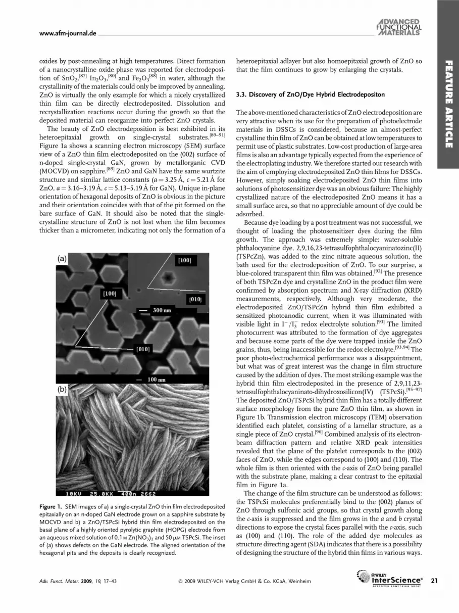
The beauty of ZnO electrodeposition is best exhibited in itsheteroepitaxial growth on single-crystal substrates.[89–91]
Figure 1a shows a scanning electron microscopy (SEM) surfaceview of a ZnO thin film electrodeposited on the (002) surface ofn-doped single-crystal GaN, grown by metallorganic CVD(MOCVD) on sapphire.[89] ZnO and GaN have the same wurtzitestructure and similar lattice constants (a¼ 3.25 A, c¼ 5.21 A forZnO, a¼ 3.16–3.19 A, c¼ 5.13–5.19 A for GaN). Unique in-planeorientation of hexagonal deposits of ZnO is obvious in the pictureand their orientation coincides with that of the pit formed on thebare surface of GaN. It should also be noted that the single-crystalline structure of ZnO is not lost when the film becomesthicker than a micrometer, indicating not only the formation of a
Figure 1. SEM images of a) a single-crystal ZnO thin film electrodeposited
epitaxially on an n-doped GaN electrode grown on a sapphire substrate by
MOCVD and b) a ZnO/TSPcSi hybrid thin film electrodeposited on the
basal plane of a highly oriented pyrolytic graphite (HOPG) electrode from
an aqueous mixed solution of 0.1 M Zn(NO3)2 and 50mM TSPcSi. The inset
of (a) shows defects on the GaN electrode. The aligned orientation of the
hexagonal pits and the deposits is clearly recognized.
Adv. Funct. Mater. 2009, 19, 17–43 � 2009 WILEY-VCH Verl
heteroepitaxial adlayer but also homoepitaxial growth of ZnO sothat the film continues to grow by enlarging the crystals.
3.3. Discovery of ZnO/Dye Hybrid Electrodepositon
The above-mentioned characteristics of ZnOelectrodeposition arevery attractive when its use for the preparation of photoelectrodematerials in DSSCs is considered, because an almost-perfectcrystalline thin film ofZnO can be obtained at low temperatures topermit use of plastic substrates. Low-cost production of large-areafilms is also an advantage typically expected from the experience ofthe electroplating industry.We therefore started our research withthe aim of employing electrodeposited ZnO thin films for DSSCs.However, simply soaking electrodeposited ZnO thin films intosolutions of photosensitizer dyewas an obvious failure: The highlycrystallized nature of the electrodeposited ZnO means it has asmall surface area, so that no appreciable amount of dye could beadsorbed.
Because dye loading by a post treatment was not successful, wethought of loading the photosensitizer dyes during the filmgrowth. The approach was extremely simple: water-solublephthalocyanine dye, 2,9,16,23-tetrasulfophthalocyaninatozinc(II)(TSPcZn), was added to the zinc nitrate aqueous solution, thebath used for the electrodeposition of ZnO. To our surprise, ablue-colored transparent thin film was obtained.[92] The presenceof both TSPcZn dye and crystalline ZnO in the product film wereconfirmed by absorption spectrum and X-ray diffraction (XRD)measurements, respectively. Although very moderate, theelectrodeposited ZnO/TSPcZn hybrid thin film exhibited asensitized photoanodic current, when it was illuminated withvisible light in I�=I�3 redox electrolyte solution.[93] The limitedphotocurrent was attributed to the formation of dye aggregatesand because some parts of the dye were trapped inside the ZnOgrains, thus, being inaccessible for the redox electrolyte.[93,94] Thepoor photo-electrochemical performance was a disappointment,but what was of great interest was the change in film structurecaused by the addition of dyes. Themost striking example was thehybrid thin film electrodeposited in the presence of 2,9,11,23-tetrasulfophthalocyaninato-dihydroxosilicon(IV) (TSPcSi).[95–97]
The deposited ZnO/TSPcSi hybrid thin film has a totally differentsurface morphology from the pure ZnO thin film, as shown inFigure 1b. Transmission electron microscopy (TEM) observationidentified each platelet, consisting of a lamellar structure, as asingle piece of ZnO crystal.[96] Combined analysis of its electron-beam diffraction pattern and relative XRD peak intensitiesrevealed that the plane of the platelet corresponds to the (002)faces of ZnO, while the edges correspond to (100) and (110). Thewhole film is then oriented with the c-axis of ZnO being parallelwith the substrate plane, making a clear contrast to the epitaxialfilm in Figure 1a.
The change of the film structure can be understood as follows:the TSPcSi molecules preferentially bind to the (002) planes ofZnO through sulfonic acid groups, so that crystal growth alongthe c-axis is suppressed and the film grows in the a and b crystaldirections to expose the crystal faces parallel with the c-axis, suchas (100) and (110). The role of the added dye molecules asstructure directing agent (SDA) indicates that there is a possibilityof designing the structure of the hybrid thin films in various ways.
ag GmbH & Co. KGaA, Weinheim 21
FEATUREARTIC
LE
www.afm-journal.de
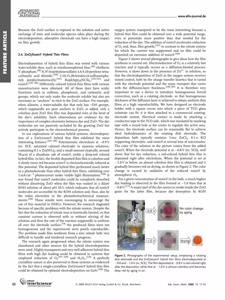
Figure 2. Photographs of the experimental setup, employing a rotating
disk electrode and the ZnO/eosinY hybrid thin films electrodeposited at
�0.8 and�1.0 V (vs. SCE). The film deposited at�0.8 V is red colored right
after the deposition, while that at �1.0 V is almost colorless and becomes
deep red by aging in air.
22
Because the ZnO surface is exposed to the solution and activeexchange of ionic and molecular species takes place during theelectrodeposition, adsorptive chemicals can have a high impacton film growth.
3.4. ZnO/EosinY Hybrid Thin Films
Electrodeposition of hybrid thin films was tested with variouswater-soluble dyes, such as tetrabromophenol blue,[98] riboflavin50-phosphate,[99]N,N0-bis(ethylenesulfate)-3,4,9,10-perylene tetra-carboxylic acid diimide,[100] 5,10,15,20-tetrakis-(4-sulfonatophe-nyl) porphyrinatozinc(II),[101] Ru(dcbpy)2(NCS)2,
[102,103] andeosinY.[104–106] Differently colored hybrid thin films with variousnanostructures were obtained. All of these dyes have acidicfunctions such as sulfonic, phosphonic, and carboxylic acidgroups, which not only make the molecule soluble but also arenecessary as ‘‘anchors’’ to stick to the ZnO surface. For example,when alizarin, a water-soluble dye that only has –OH groups,which supposedly are poor anchors to ZnO, is added, only acolorless pure ZnO thin film was deposited even at the limit ofthe dye’s solubility. Such observations are evidence for theimportance of complex chemistry between dye and ZnO. The dyemolecules are not passively occluded by the growing ZnO butactively participate in the electrochemical process.
In our explorations of various hybrid systems, electrodeposi-tion of a ZnO/eosinY hybrid thin film exhibited the mostinteresting features.[104–106] Potentiostatic electrolysis at �0.9 V(vs. SCE, saturated calomel electrode) in aqueous solutions,containing 0.1 M Zn(NO3)2 and a small amount (typically, around50mM) of a disodium salt of eosinY, yields a deep-red coloredhybrid film. In fact, the freshly deposited thin film is colorless andit slowly turns red because eosinY is electrochemically reduced atthis potential. The deposited hybrid film performed much betteras a photoelectrode than other hybrid thin films, exhibiting over1mAcm�2 photocurrent under visible light illumination.[106] Itwas found that eosinY molecules could be completely desorbedwithout dissolving ZnO when the film was soaked in a diluteKOH solution of about pH 10.5, which indicates that all eosinYmolecules are accessible by the KOH solution and, thus, also bythe redox electrolyte in the photoelectrochemical measure-ments.[106] These results were encouraging to encourage theuse of this material in DSSCs. However, the research stagnatedbecause of specific problems with the nitrate system. Despite thefact that the reduction of nitrate ions is kinetically limited, so thatconstant current is observed with or without stirring of thesolution and thus the rate of the reaction supposedly is uniformall over the electrode surface,[78] the produced films were nothomogeneous and the experiments were poorly reproducible.The problem made film synthesis from a zinc nitrate bath verydifficult to handle and hindered research progress.
The research again progressed when the nitrate system wasabandoned and other sources for the hybrid electrodepositionwere used. Highly transparent and very well adherent hybrid thinfilms with high dye loading could be obtained in systems thatemployed reduction of O2
[107–109] and H2O2.[110] A perfectly
crystalline nature is also preserved in these systems as evidencedby the fact that a single-crystalline ZnO/eosinY hybrid thin filmcould be obtained by epitaxial electrodeposition on GaN.[108] The
� 2009 WILEY-VCH Verlag GmbH
oxygen system transpired to be the most interesting because ahybrid thin film could be obtained over a wide potential range,even at potentials more positive than that needed for thereduction of the dye. The addition of eosinYaccelerates reductionof O2 and, thus, film growth,[107] in contrast to the nitrate systemfor which the current was suppressed and no film could bedeposited on excessive addition of eosinY.[106]
Figure 2 shows several photographs to give ideas how the filmsynthesis is carried out. Electroreduction of O2 is a relatively fastreaction and it typically occurs as a diffusion-limited process.However, it slows down in the presence of Zn2þ in solution, sothat the electrodeposition of ZnO in the oxygen system receivesmixed control, both by the charge transfer kinetics that is variedwith the electrode potential and the mass transport that varieswith the diffusion-layer thickness.[108,109] It is therefore veryimportant to use a device to introduce homogeneous forcedconvection, such as a rotating electrode, so that homogeneousthickness of the diffusion layer is achieved to obtain uniform thinfilms at a high reproducibility. We have designed an electrodeholder with a square recess into which a piece of TCO glasssubstrate can fit; it is then attached to a commercial rotating-electrode system. Electrical contact is made by attaching aconductive tape to the TCO side, which was insulated by maskingtape with a round hole at the center to regulate the active area.Hence, the electrode surface can be reasonably flat to achieveideal hydrodynamics of the rotating disk electrode. Thedeposition bath typically contains 5mM ZnCl2, 0.1 M KClsupporting electrolyte, and eosinY at several tens of micromoles.The color of the solution in the picture comes from the addedeosinY. When the electrode potential is at �0.8 V (vs. SCE), wellabove that for dye reduction, a red-colored hybrid thin film isdeposited right after electrolysis. When the potential is set at�1.0 V or below, an almost colorless thin film is obtained and itgradually becomes red on drying, as shown in Figure 2. The colorchange is caused by oxidation of the reduced eosinY byatmospheric O2.
For a given concentration of eosinY in the bath, a much higherdye loading is observed in the film formed at �1.0 than that at�0.8 V.[113] Amajor part of the dye seems to reside inside the ZnOgrain for the latter film, because dye desorption by KOH
& Co. KGaA, Weinheim Adv. Funct. Mater. 2009, 19, 17–43
FEATUREARTIC
LE
www.afm-journal.de
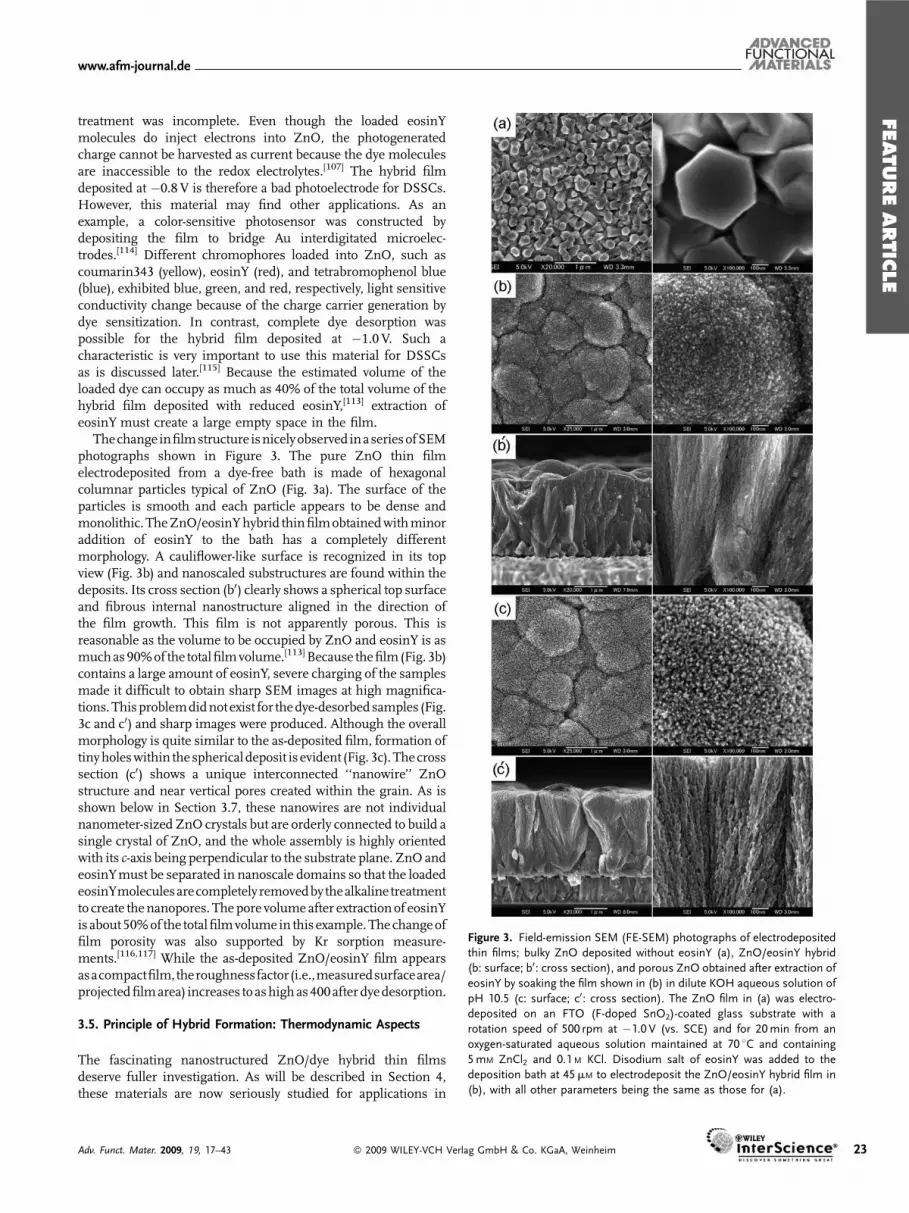
Figure 3. Field-emission SEM (FE-SEM) photographs of electrodeposited
thin films; bulky ZnO deposited without eosinY (a), ZnO/eosinY hybrid
(b: surface; b0: cross section), and porous ZnO obtained after extraction of
eosinY by soaking the film shown in (b) in dilute KOH aqueous solution of
pH 10.5 (c: surface; c0: cross section). The ZnO film in (a) was electro-
deposited on an FTO (F-doped SnO2)-coated glass substrate with a
rotation speed of 500 rpm at �1.0 V (vs. SCE) and for 20min from an
oxygen-saturated aqueous solution maintained at 70 8C and containing
5mM ZnCl2 and 0.1 M KCl. Disodium salt of eosinY was added to the
deposition bath at 45mM to electrodeposit the ZnO/eosinY hybrid film in
(b), with all other parameters being the same as those for (a).
treatment was incomplete. Even though the loaded eosinYmolecules do inject electrons into ZnO, the photogeneratedcharge cannot be harvested as current because the dye moleculesare inaccessible to the redox electrolytes.[107] The hybrid filmdeposited at �0.8 V is therefore a bad photoelectrode for DSSCs.However, this material may find other applications. As anexample, a color-sensitive photosensor was constructed bydepositing the film to bridge Au interdigitated microelec-trodes.[114] Different chromophores loaded into ZnO, such ascoumarin343 (yellow), eosinY (red), and tetrabromophenol blue(blue), exhibited blue, green, and red, respectively, light sensitiveconductivity change because of the charge carrier generation bydye sensitization. In contrast, complete dye desorption waspossible for the hybrid film deposited at �1.0 V. Such acharacteristic is very important to use this material for DSSCsas is discussed later.[115] Because the estimated volume of theloaded dye can occupy as much as 40% of the total volume of thehybrid film deposited with reduced eosinY,[113] extraction ofeosinY must create a large empty space in the film.
Thechange infilmstructure isnicelyobserved inaseriesofSEMphotographs shown in Figure 3. The pure ZnO thin filmelectrodeposited from a dye-free bath is made of hexagonalcolumnar particles typical of ZnO (Fig. 3a). The surface of theparticles is smooth and each particle appears to be dense andmonolithic. TheZnO/eosinYhybrid thinfilmobtainedwithminoraddition of eosinY to the bath has a completely differentmorphology. A cauliflower-like surface is recognized in its topview (Fig. 3b) and nanoscaled substructures are found within thedeposits. Its cross section (b0) clearly shows a spherical top surfaceand fibrous internal nanostructure aligned in the direction ofthe film growth. This film is not apparently porous. This isreasonable as the volume to be occupied by ZnO and eosinY is asmuchas90%of the total filmvolume.[113] Because thefilm(Fig. 3b)contains a large amount of eosinY, severe charging of the samplesmade it difficult to obtain sharp SEM images at high magnifica-tions.Thisproblemdidnot exist for thedye-desorbedsamples (Fig.3c and c0) and sharp images were produced. Although the overallmorphology is quite similar to the as-deposited film, formation oftinyholeswithin the spherical deposit is evident (Fig. 3c). Thecrosssection (c0) shows a unique interconnected ‘‘nanowire’’ ZnOstructure and near vertical pores created within the grain. As isshown below in Section 3.7, these nanowires are not individualnanometer-sized ZnO crystals but are orderly connected to build asingle crystal of ZnO, and the whole assembly is highly orientedwith its c-axis being perpendicular to the substrate plane. ZnO andeosinYmust be separated in nanoscale domains so that the loadedeosinYmoleculesarecompletely removedby thealkaline treatmentto create thenanopores. Thepore volumeafter extractionof eosinYis about 50%of the total filmvolume in this example.The changeoffilm porosity was also supported by Kr sorption measure-ments.[116,117] While the as-deposited ZnO/eosinY film appearsasacompactfilm,theroughnessfactor(i.e.,measuredsurfacearea/projectedfilmarea) increases to ashighas400after dyedesorption.
3.5. Principle of Hybrid Formation: Thermodynamic Aspects
The fascinating nanostructured ZnO/dye hybrid thin filmsdeserve fuller investigation. As will be described in Section 4,these materials are now seriously studied for applications in
Adv. Funct. Mater. 2009, 19, 17–43 � 2009 WILEY-VCH Verlag GmbH & Co. KGaA, Weinheim 23

FEATUREARTIC
LE
www.afm-journal.de
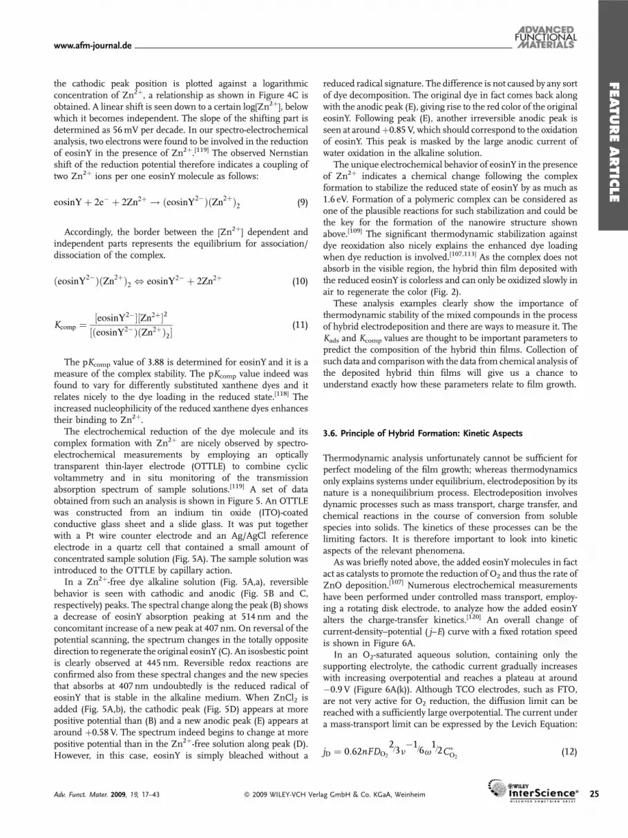
Figure 4. A) Adsorption isotherm measured by adding ZnO nanoparticlate
powder for various amounts between 0.05 and 1.5 g to 20mL of 0.2mM
eosinYaqueoussolutions (pH5.8). Themixtureswerestirredovernight in the
dark at 25 8C to establish the equilibrium. The concentration of residual dye
was then determined from the absorption spectrum of the solution after
removal of dye-adsorbed ZnO powder by filtration. Fitting to the data points
according to the Langmuir adsorption isothermal equation is indicated.
B) Cyclic voltammograms measured at a stationary FTO-coated conductive
glass electrode in aqueous solutions containing 0.5mMeosinY, 0.1 MKCl, and
ZnCl2 with different concentrations. The solutions were deaerated, by bub-
bling Ar gas, and maintained at 70 8C by a thermostat. The scan rate was
500mV s�1. C) The cathodic peak potentials plotted against logarithmic
concentration of Zn2þ. The border between the [Zn2þ] dependent and
independent regions yields the pKcomp value (see text).
24
plastic DSSCs. The self-assembly of the nanowire ZnO/eosinYhybrid, for example, should not just be an accidental finding butmust be fully understood from its basic principles, in order for usto become able to handle the process for mass production andalso for discovering new systems. We are carrying out variouschemical and electrochemical analyses to establish a model forthe electrochemical growth of the hybrid thin films taking ZnO/eosinY as a reference system. Although we are still far fromperfect understanding, several conventional experimentalapproaches already allow us to get close to it.
As repeatedlypointedoutabove, the loadingofeosinYmoleculestakes place as a spontaneous chemical reaction between electro-chemically grown ZnO and eosinY molecules either in theiroxidized or reduced states. It is therefore reasonable to try toapproach the phenomenon from its thermodynamic aspects,namely, analyzing how strongly these components like to betogether.
EosinYmolecules are adsorbed on the surface of ZnO owing tothe presence of carboxylic acid groups. When ZnO powder is putinto a solution of eosinY, one can see the red coloring of thepowder. The colored powder can be washed by a mild alkalinesolution to desorb the dye and regain the colorless ZnO. Anadsorption isotherm can be drawn by adding a controlled amountof ZnO into the dye solution, waiting for some time to establishequilibrium and measure the amount of dye left in thesupernatant. An example of such analysis for an aqueoussolution of eosinY is shown in Figure 4A. Xanthene dyesincluding eosinY actually undergo Langmuir-type monolayeradsorption for which the equilibrium is established according tothe following equation:
m ¼ KadscM
Kadsc þ 1(8)
wherem is the amount of adsorbed dye in equilibrium (in units of
mol g�1 of ZnO),M is the saturation amount (mol g�1 ZnO), c isthe concentration of dye solution in equilibrium [M], and Kads is
the adsorption stability constant [M�1]. From the fitting,
M¼ 11.3� 10�6mol g�1 ZnO and Kads¼ 76 900 M�1 are deter-
mined for this system. If the adsorption/desorption equilibrium
is maintained during the film growth, the composition of the
hybrid film must be under the control of the adsorption stability.
We have carried out such an analysis for 5(6)-carboxyeosin, which
has an extra carboxylic acid group and 2,4,5,7-tetrabromosulfo-
fluorescein substituting the carboxylic group of eosinY with
sulfonic acid group, in comparison with eosinY.[118] Much larger
and smaller Kads values were found for dicarboxylated and
sulfonated eosinY, respectively, indicating the higher stability of
coordination of the carboxylic acid group than the sulfonic acid
group. The loading of the dyes in their oxidized state was in good
agreement with the order of the adsorption stability.When the electrodeposition is carried out at potentials more
negative than about �0.9 V, these xanthene dyes are reduced andloaded into the film in a much larger amount than in theiroxidized state. The change is caused by the increased stability ofdye attachment because of formation of a stable complex betweenthe reduced dye and Zn2þ ions.[106] The complex formation can beevidenced and analyzed from a series of cyclic voltammograms
� 2009 WILEY-VCH Verlag GmbH
measured for the dye solution containing varying concentrationsof Zn2þ (Fig. 4B). In eosinYsolution free of Zn2þ, reversible redoxpeaks centered at �1.03V vs. SCE are seen. Upon increasing theZn2þ addition, the cathodic peak position shifts positively and theanodic peak corresponding to dye reoxidation diminishes. When
& Co. KGaA, Weinheim Adv. Funct. Mater. 2009, 19, 17–43
FEATUREARTIC
LE
www.afm-journal.de
the cathodic peak position is plotted against a logarithmicconcentration of Zn2þ, a relationship as shown in Figure 4C isobtained. A linear shift is seen down to a certain log[Zn2þ], belowwhich it becomes independent. The slope of the shifting part isdetermined as 56mV per decade. In our spectro-electrochemicalanalysis, two electrons were found to be involved in the reductionof eosinY in the presence of Zn2þ.[119] The observed Nernstianshift of the reduction potential therefore indicates a coupling oftwo Zn2þ ions per one eosinY molecule as follows:
eosinYþ 2e� þ 2Zn2þ ! ðeosinY2�ÞðZn2þÞ2 (9)
Accordingly, the border between the [Zn2þ] dependent andindependent parts represents the equilibrium for association/dissociation of the complex.
ðeosinY2�ÞðZn2þÞ2 , eosinY2� þ 2Zn2þ (10)
Kcomp ¼½eosinY2��½Zn2þ�2
½ðeosinY2�ÞðZn2þÞ2�(11)
The pKcomp value of 3.88 is determined for eosinY and it is ameasure of the complex stability. The pKcomp value indeed wasfound to vary for differently substituted xanthene dyes and itrelates nicely to the dye loading in the reduced state.[118] Theincreased nucleophilicity of the reduced xanthene dyes enhancestheir binding to Zn2þ.
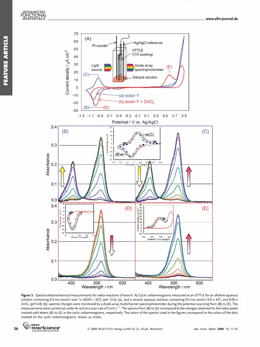
The electrochemical reduction of the dye molecule and itscomplex formation with Zn2þ are nicely observed by spectro-electrochemical measurements by employing an opticallytransparent thin-layer electrode (OTTLE) to combine cyclicvoltammetry and in situ monitoring of the transmissionabsorption spectrum of sample solutions.[119] A set of dataobtained from such an analysis is shown in Figure 5. An OTTLEwas constructed from an indium tin oxide (ITO)-coatedconductive glass sheet and a slide glass. It was put togetherwith a Pt wire counter electrode and an Ag/AgCl referenceelectrode in a quartz cell that contained a small amount ofconcentrated sample solution (Fig. 5A). The sample solution wasintroduced to the OTTLE by capillary action.
In a Zn2þ-free dye alkaline solution (Fig. 5A,a), reversiblebehavior is seen with cathodic and anodic (Fig. 5B and C,respectively) peaks. The spectral change along the peak (B) showsa decrease of eosinY absorption peaking at 514 nm and theconcomitant increase of a new peak at 407 nm. On reversal of thepotential scanning, the spectrum changes in the totally oppositedirection to regenerate the original eosinY (C). An isosbestic pointis clearly observed at 445 nm. Reversible redox reactions areconfirmed also from these spectral changes and the new speciesthat absorbs at 407 nm undoubtedly is the reduced radical ofeosinY that is stable in the alkaline medium. When ZnCl2 isadded (Fig. 5A,b), the cathodic peak (Fig. 5D) appears at morepositive potential than (B) and a new anodic peak (E) appears ataround þ0.58 V. The spectrum indeed begins to change at morepositive potential than in the Zn2þ-free solution along peak (D).However, in this case, eosinY is simply bleached without a
Adv. Funct. Mater. 2009, 19, 17–43 � 2009 WILEY-VCH Verl
reduced radical signature. The difference is not caused by any sortof dye decomposition. The original dye in fact comes back alongwith the anodic peak (E), giving rise to the red color of the originaleosinY. Following peak (E), another irreversible anodic peak isseen at aroundþ0.85V, which should correspond to the oxidationof eosinY. This peak is masked by the large anodic current ofwater oxidation in the alkaline solution.
The unique electrochemical behavior of eosinY in the presenceof Zn2þ indicates a chemical change following the complexformation to stabilize the reduced state of eosinY by as much as1.6 eV. Formation of a polymeric complex can be considered asone of the plausible reactions for such stabilization and could bethe key for the formation of the nanowire structure shownabove.[109] The significant thermodynamic stabilization againstdye reoxidation also nicely explains the enhanced dye loadingwhen dye reduction is involved.[107,113] As the complex does notabsorb in the visible region, the hybrid thin film deposited withthe reduced eosinY is colorless and can only be oxidized slowly inair to regenerate the color (Fig. 2).
These analysis examples clearly show the importance ofthermodynamic stability of the mixed compounds in the processof hybrid electrodeposition and there are ways to measure it. TheKads and Kcomp values are thought to be important parameters topredict the composition of the hybrid thin films. Collection ofsuch data and comparison with the data from chemical analysis ofthe deposited hybrid thin films will give us a chance tounderstand exactly how these parameters relate to film growth.
3.6. Principle of Hybrid Formation: Kinetic Aspects
Thermodynamic analysis unfortunately cannot be sufficient forperfect modeling of the film growth; whereas thermodynamicsonly explains systems under equilibrium, electrodeposition by itsnature is a nonequilibrium process. Electrodeposition involvesdynamic processes such as mass transport, charge transfer, andchemical reactions in the course of conversion from solublespecies into solids. The kinetics of these processes can be thelimiting factors. It is therefore important to look into kineticaspects of the relevant phenomena.
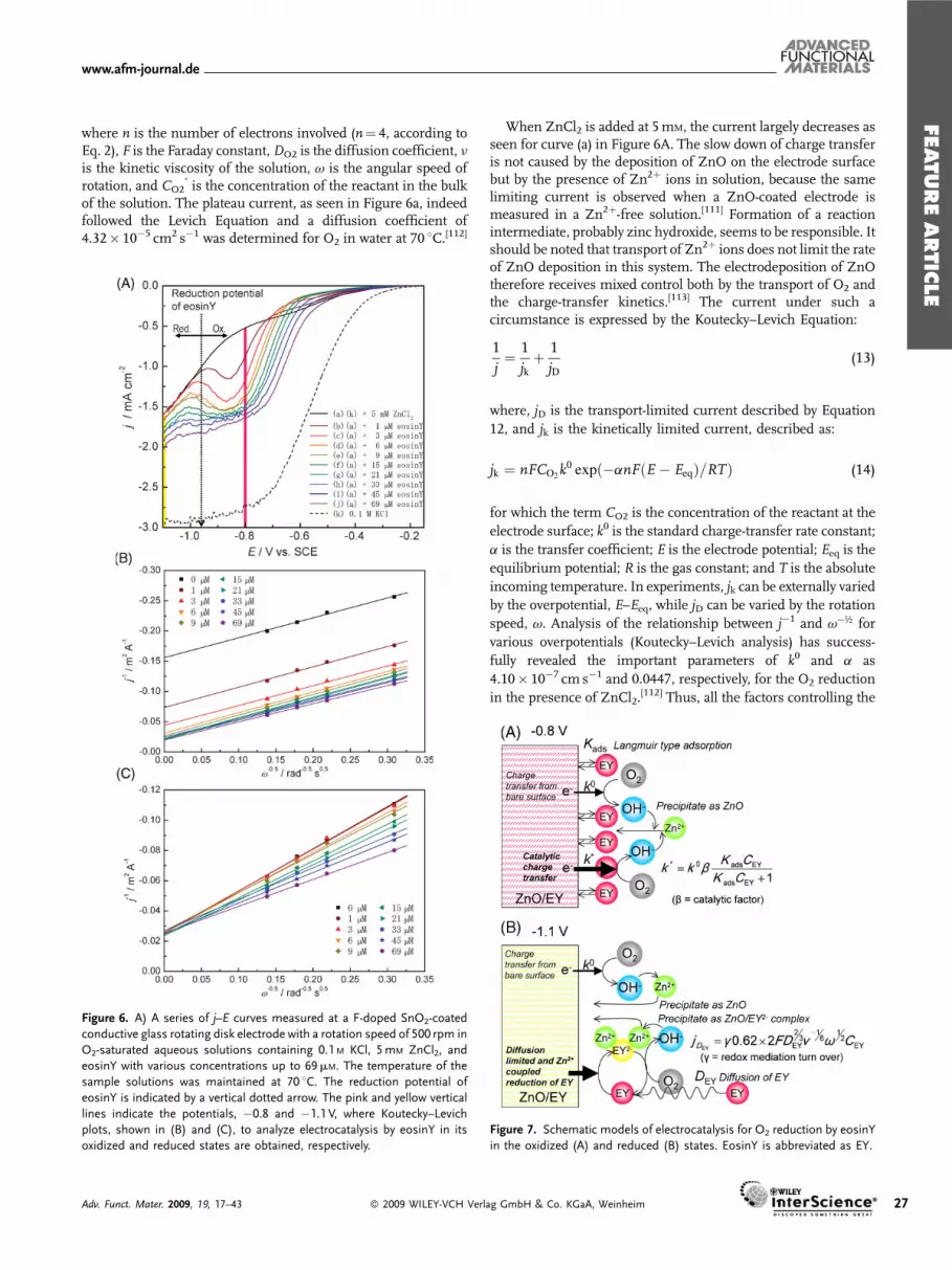
As was briefly noted above, the added eosinYmolecules in factact as catalysts to promote the reduction of O2 and thus the rate ofZnO deposition.[107] Numerous electrochemical measurementshave been performed under controlled mass transport, employ-ing a rotating disk electrode, to analyze how the added eosinYalters the charge-transfer kinetics.[120] An overall change ofcurrent-density–potential ( j–E) curve with a fixed rotation speedis shown in Figure 6A.
In an O2-saturated aqueous solution, containing only thesupporting electrolyte, the cathodic current gradually increaseswith increasing overpotential and reaches a plateau at around�0.9 V (Figure 6A(k)). Although TCO electrodes, such as FTO,are not very active for O2 reduction, the diffusion limit can bereached with a sufficiently large overpotential. The current undera mass-transport limit can be expressed by the Levich Equation:
jD ¼ 0:62nFDO2
2=3n�1=6v
1=2C�O2
(12)
ag GmbH & Co. KGaA, Weinheim 25
FEATUREARTIC
LE
www.afm-journal.de
Figure 5. Spectro-electrochemical measurements for redox reactions of eosinY: A) Cyclic voltammograms measured at an OTTLE for an alkaline aqueous
solution containing 0.5mM eosinY and 1M (KOHþKCl) (pH 12.6) (a), and a neutral aqueous solution containing 0.5mM eosinY, 0.9 M KCl, and 0.05 M
ZnCl2 (pH 6.8) (b); spectral changes were monitored by a diode array multichannel spectrophotometer during the potential scanning from (B) to (E). The
measurements were carried out under Ar and at a scan rate of 5mV s�1. The spectra from (B) to (E) correspond to the changes observed for the redox peaks
marked with letters (B) to (E) in the cyclic voltammograms, respectively. The colors of the spectra used in the figures correspond to the colors of the dots
marked on the cyclic voltammograms, shown as insets.
26 � 2009 WILEY-VCH Verlag GmbH & Co. KGaA, Weinheim Adv. Funct. Mater. 2009, 19, 17–43
FEATUREAR
www.afm-journal.de
where n is the number of electrons involved (n¼ 4, according toEq. 2), F is the Faraday constant,DO2 is the diffusion coefficient, nis the kinetic viscosity of the solution, v is the angular speed ofrotation, and CO2
�is the concentration of the reactant in the bulk
of the solution. The plateau current, as seen in Figure 6a, indeedfollowed the Levich Equation and a diffusion coefficient of4.32� 10�5 cm2 s�1 was determined for O2 in water at 70 8C.[112]
TICLE
Figure 6. A) A series of j–E curves measured at a F-doped SnO2-coated
conductive glass rotating disk electrode with a rotation speed of 500 rpm in
O2-saturated aqueous solutions containing 0.1 M KCl, 5mM ZnCl2, and
eosinY with various concentrations up to 69mM. The temperature of the
sample solutions was maintained at 70 8C. The reduction potential of
eosinY is indicated by a vertical dotted arrow. The pink and yellow vertical
lines indicate the potentials, �0.8 and �1.1 V, where Koutecky–Levich
plots, shown in (B) and (C), to analyze electrocatalysis by eosinY in its
oxidized and reduced states are obtained, respectively.
Adv. Funct. Mater. 2009, 19, 17–43 � 2009 WILEY-VCH Verl
When ZnCl2 is added at 5mM, the current largely decreases asseen for curve (a) in Figure 6A. The slow down of charge transferis not caused by the deposition of ZnO on the electrode surfacebut by the presence of Zn2þ ions in solution, because the samelimiting current is observed when a ZnO-coated electrode ismeasured in a Zn2þ-free solution.[111] Formation of a reactionintermediate, probably zinc hydroxide, seems to be responsible. Itshould be noted that transport of Zn2þ ions does not limit the rateof ZnO deposition in this system. The electrodeposition of ZnOtherefore receives mixed control both by the transport of O2 andthe charge-transfer kinetics.[113] The current under such acircumstance is expressed by the Koutecky–Levich Equation:
1
j¼ 1
jkþ 1
jD(13)
where, jD is the transport-limited current described by Equation
12, and jk is the kinetically limited current, described as:
jk ¼ nFCO2k0 expð�anFðE � EeqÞ=RTÞ (14)
for which the term CO2 is the concentration of the reactant at the
electrode surface; k0 is the standard charge-transfer rate constant;
a is the transfer coefficient; E is the electrode potential; Eeq is theequilibrium potential; R is the gas constant; and T is the absolute
incoming temperature. In experiments, jk can be externally varied
by the overpotential, E–Eeq, while jD can be varied by the rotation
speed, v. Analysis of the relationship between j�1 and v�½ for
various overpotentials (Koutecky–Levich analysis) has success-
fully revealed the important parameters of k0 and a as
4.10� 10�7 cm s�1 and 0.0447, respectively, for the O2 reduction
in the presence of ZnCl2.[112] Thus, all the factors controlling the
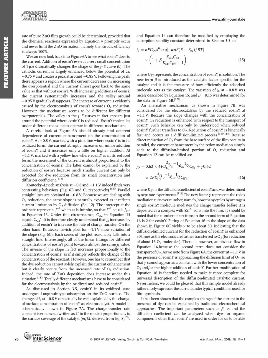
Figure 7. Schematic models of electrocatalysis for O2 reduction by eosinY
in the oxidized (A) and reduced (B) states. EosinY is abbreviated as EY.
ag GmbH & Co. KGaA, Weinheim 27
FEATUREARTIC
LE
www.afm-journal.de
28
rate of pure ZnO film growth could be determined, provided that
the chemical reactions expressed by Equation 4 promptly occur
and never limit the ZnO formation; namely, the Faradic efficiency
is always 100%.We can now look back into Figure 6A to see what eosinYdoes to
the current. Addition of eosinYeven at a very small concentrationof 1mM dramatically changes the shape of the j–E curve (b). Thecathodic current is largely enhanced below the potential of ca.�0.75Vand creates a peak at around�0.85V. Following the peak,there appears a region where the current decreases on increasingthe overpotential and the current almost goes back to the samevalue as that without eosinY. With increasing additions of eosinY,the current systematically increases and the valley around�0.95Vgradually disappears. The increase of current is evidentlycaused by the electrocatalysis of eosinY towards O2 reduction.However, the mechanism seems to be different for differentoverpotentials. The valley in the j–E curves in fact appears justaround the potential where eosinY is reduced. EosinYmoleculesunder different redox states operate in different mechanisms.
A careful look at Figure 6A should already find deferentdependence of current enhancement on the concentration ofeosinY. At �0.8 V, marked with a pink line where eosinY is in itsoxidized form, the current abruptly increases on minor additionof eosinY and it increases only a little on higher addition. At�1.1 V, marked with a yellow line where eosinY is in its reducedform, the increment of the current is almost proportional to theconcentration of eosinY. The latter cannot be explained by thereduction of eosinY because much smaller current can only beexpected for dye reduction from its small concentration anddiffusion coefficient.[118]
Koutecky–Levich analysis at�0.8 and�1.1 V indeed finds verycontrasting behaviors (Fig. 6B and C, respectively).[120] Parallelstraight lines are obtained at �0.8 V. Because we are dealing withO2 reduction, the same slope is naturally expected as it reflectscurrent limitation by O2 diffusion (Eq. 12). The intercept at theordinate represents j�1 when v is infinite, so that j�1 equals jk�1
in Equation 13. Under this circumstance, CO2 in Equation 14equals CO2
�. It is therefore clearly understood that jk increases byaddition of eosinY to increase the rate of charge transfer. On theother hand, Koutecky–Levich plots for �1.1 V show variation ofthe slope (Fig. 6C). Each series of the plot reasonably falls into astraight line. Interestingly, all of the linear fittings for differentconcentrations of eosinY point towards almost the same jk value.The inverse of the slope in fact increases proportionally to theconcentration of eosinY, as if it simply reflects the change of theconcentration of the reactant. However, one has to remember thatthe dye reduction cannot solely explain the current enhancementbut it clearly occurs from the increased rate of O2 reduction.Indeed, the rate of ZnO deposition does increase under thissituation.[113] Totally different mechanisms have to be consideredfor the electrocatalysis by the oxidized and reduced eosinY.
As discussed in Section 3.5, eosinY in its oxidized stateundergoes Langmuir-type adsorption on the ZnO surface. Thechange of jk at�0.8 V can actually be well explained by the changeof surface concentration of eosinY as electrocatalyst. A model isschematically shown in Figure 7A. The charge-transfer rateconstant is enhanced (written as k� in themodel) proportionally tothe surface coverage of the catalyst (m/M, derived from Eq. 8)[78],
� 2009 WILEY-VCH Verlag GmbH
and Equation 14 can therefore be modified by employing theadsorption stability constant determined in Section 3.5 as:
jk ¼ nFCO2k0 exp½�anFðE � EeqÞ=RT �
� 1þ bKadsCEY
KadsCEY þ 1
� �(15)
whereCEYrepresents the concentration of eosinY in solution. The
new term b is introduced as the catalytic factor specific for the
catalyst and it is the measure of how efficiently the adsorbed
molecule acts as the catalyst. The variation of jk at �0.8 V was
nicely described by Equation 15, and b¼ 8.15 was determined for
the data in Figure 6B.[120]
An alternative mechanism, as shown in Figure 7B, wasconsidered for the electrocatalysis by the reduced eosinY at�1.1 V. Because the slope changes with the concentration ofeosinY, O2 reduction is enhanced with respect to the transport ofeosinY. Such behavior can only be understood when reducedeosinY further transfers to O2. Reduction of eosinY is kineticallyfast and occurs as a diffusion-limited process.[110,118] Becausedirect reduction of O2 from the bare surface of the film occurs inparallel, the current enhancement by the redox mediation simplyadds to the diffusion-limited portion of O2 reduction andEquation 12 can be modified as:
jD ¼ 0:62� 4FD2=3O2
n�1=6v
1=2CO2þ g0:62
� 2FD2=3EY n
�1=6v1=2CEY (16)
whereDEY is thediffusioncoefficient of eosinYandwasdetermined
by separate experiments.[118] The new factor g represents the redox
mediation turnover number, namely, howmany cycles by average a
single eosinY molecule mediates the charge transfer before it is
deposited as a complex with Zn2þ ions into the film. It should be
noted that the number of electrons in the second term of Equation
16 is 2 for eosinY. Fitting of Equation 16 to the slope of the data
shown in Figure 6C yields g to be about 30, indicating that the
diffusion-limited current for the reduction of eosinY is enhanced
30 times as the electrons are further transferred toO2 (for reduction
of about 15 O2 molecules). There is, however, an obvious flaw in
Equation 16,because the second term does not consider the
transport ofO2. Aswenote fromFigure 6A, the current at�1.1V in
the presence of eosinY is approaching the diffusion limit of O2, so
that g cannot appear as a constant with the lower concentration of
O2 and/or the higher addition of eosinY. Further modification of
Equation 16 is therefore needed to make it more complete for
universal description of the diffusion-limited catalytic current.
Nevertheless, we could be pleased that this simple model already
rathernicelyexpresses the currentunder typical conditionsused for
film synthesis.It has been shown that the complex change of the current in the
presence of dye can be explained by traditional electrochemicalapproaches. The important parameters such as b, g , and thediffusion coefficient can be analyzed when dyes or organiccomponents other than eosinY are used in order for us to be able
& Co. KGaA, Weinheim Adv. Funct. Mater. 2009, 19, 17–43
FEATUREARTIC
LE
www.afm-journal.de
Figure 8. Transmission electron microscopy (TEM) images of an as-
deposited ZnO/eosinY hybrid thin film made into a thin specimen by a
focused ion-beam (FIB) system: the low-magnification image and selected-
area electron beam diffraction (SAED) pattern, shown as an inset, were
taken for the part marked by a circle in image (A). B) The high-resolution
image showing lattice fringes that correspond to the (002) spacing of ZnO.
The SAED spots can be assigned with respect to the [010] zone axis, as
indexed in the figure. The hybrid thin film was electrodeposited at �1.0 V
(vs. SCE) from a bath containing 45mM eosinY.
to ‘‘predict’’ the rate of ZnO growth under given syntheticconditions. Many challenges, however, remain for perfect under-standing of the hybrid film growth. For example, there is thequestion of if we can describe the catalytic current by eosinY in thepotential range between �0.8 and �1.1V by blend of the twomechanisms. Although Faradic efficiency was found to be almost100% for typical electrodeposition of ZnO/eosinY hybrid thinfilms,[113] there isnoguarantee that thechemical reactionkineticsofEquation 4 never limits the rate of ZnO formation. There is also thequestionofwhether the rate of dye loading into thefilm isunder thecontrol of the thermodynamic stability of adsorption, or whetherdynamic processes such as dye transport and the chemical reactionkinetics of bond formation with ZnO come into play. Under-standing of the nanostructure of the hybrid films is a separatequestion that cannotbesimply answeredby theanalysisof chemicalcomposition but needs direct observations, as described in thefollowing sections. Answering these questions needs many moreexperiments, not only electrochemical analysis but also analyses ofthe actual film synthesis and of the products to check the validity ofthe model. There is a long way to go. But having completed suchstudies, we can reach a situationwhere the hybrid electrodepositonis no longer a ‘‘mystery’’ but something perfectly understandableand industrially maneuverable.
3.7. Nanostructured Porous Crystals
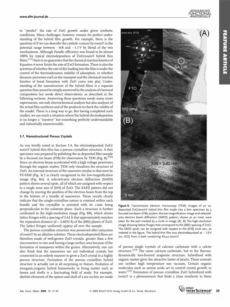
As was briefly noted in Section 3.4, the electrodeposited ZnO/eosinY hybrid thin film has a porous crystalline structure. A thinspecimen was prepared by polishing the as-deposited film sampleby a focused ion beam (FIB) for observation by TEM (Fig. 8).[120]
Since an electron beam accelerated with a high voltage penetratesthrough the organic matter, TEM only visualizes the structure ofZnO. An internal structure of the nanowire similar to that seen byFE-SEM (Fig. 3c0) is clearly recognized in the low-magnificationimage (Fig. 8A). A selected-area electron diffraction (SAED)pattern shows several spots, all of which are assigned with respectto a single zone axis of [010] of ZnO. The SAED pattern did notchange by moving the position of the electron beam from the topto the bottom of a bundle of nanowires. These results clearlyindicate that the single-crystalline nature is retained within eachbundle and the crystallite is oriented with its c-axis beingperpendicular to the substrate plane. Such a structure is furtherconfirmed in the high-resolution image (Fig. 8B), which showslattice fringes with a spacing of 2.62 A that approximately matchesthe separation distance (d¼ 2.6033 A) of the (002) planes of ZnO.The lattice fringes uniformly appear all over the sample.
The porous crystalline structure was preserved after extractionof eosinY by an alkaline solution. These electrodeposited films aretherefore made of well-grown ZnO crystals, greater than a fewmicrometers in size and having a large surface area because of theformation of nanopores within the grains. Alternatively, one canalso think that the nanowires are not individual crystals butconnected in an orderly manner to grow a ZnO crystal in a highlyporous structure. Formation of the porous crystalline hybridstructure is actually not at all surprising in Nature. Evolution ofinorganic/organic hybrid frameworks in living matter such asbones and shells is a fascinating field of study. For example,skeletal elements of the spines and shell of a sea urchin are made
Adv. Funct. Mater. 2009, 19, 17–43 � 2009 WILEY-VCH Verl
of porous single crystals of calcium carbonate with a calcitestructure.[122] The same calcium carbonate, but in the thermo-dynamically less-favored aragonite structure, hybridized withorganic matter gives the attractive luster of pearls. These animalsuse neither high temperature nor vacuum. Certain organicmolecules such as amino acids act to control crystal growth inwater.[123] Formation of porous crystalline ZnO hybridized witheosinY is a phenomenon that finds a close similarity to these
ag GmbH & Co. KGaA, Weinheim 29
FEATUREARTIC
LE
www.afm-journal.de
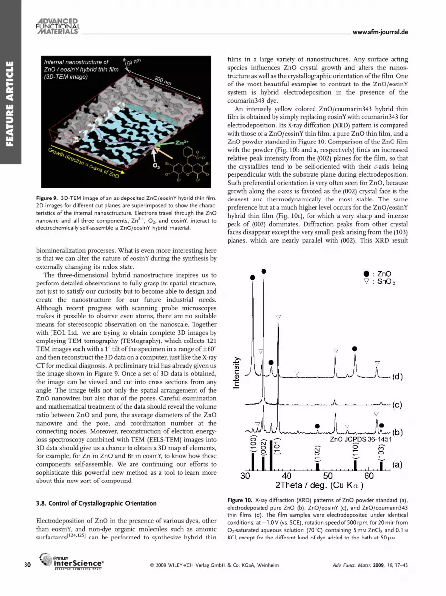
Figure 9. 3D-TEM image of an as-deposited ZnO/eosinY hybrid thin film.
2D images for different cut planes are superimposed to show the charac-
teristics of the internal nanosctructure. Electrons travel through the ZnO
nanowire and all three components, Zn2þ, O2, and eosinY, interact to
electrochemically self-assemble a ZnO/eosinY hybrid material.
Figure 10. X-ray diffraction (XRD) patterns of ZnO powder standard (a),
electrodeposited pure ZnO (b), ZnO/eosinY (c), and ZnO/coumarin343
thin films (d). The film samples were electrodeposited under identical
conditions: at�1.0 V (vs. SCE), rotation speed of 500 rpm, for 20min from
O2-saturated aqueous solution (70 8C) containing 5mM ZnCl2 and 0.1 M
KCl, except for the different kind of dye added to the bath at 50mM.
30
biomineralization processes. What is even more interesting hereis that we can alter the nature of eosinY during the synthesis byexternally changing its redox state.
The three-dimensional hybrid nanostructure inspires us toperform detailed observations to fully grasp its spatial structure,not just to satisfy our curiosity but to become able to design andcreate the nanostructure for our future industrial needs.Although recent progress with scanning probe microscopesmakes it possible to observe even atoms, there are no suitablemeans for stereoscopic observation on the nanoscale. Togetherwith JEOL Ltd., we are trying to obtain complete 3D images byemploying TEM tomography (TEMography), which collects 121TEM images each with a 18 tilt of the specimen in a range of�608and then reconstruct the 3D data on a computer, just like the X-rayCT for medical diagnosis. A preliminary trial has already given usthe image shown in Figure 9. Once a set of 3D data is obtained,the image can be viewed and cut into cross sections from anyangle. The image tells not only the spatial arrangement of theZnO nanowires but also that of the pores. Careful examinationand mathematical treatment of the data should reveal the volumeratio between ZnO and pore, the average diameters of the ZnOnanowire and the pore, and coordination number at theconnecting nodes. Moreover, reconstruction of electron energy-loss spectroscopy combined with TEM (EELS-TEM) images into3D data should give us a chance to obtain a 3D map of elements,for example, for Zn in ZnO and Br in eosinY, to know how thesecomponents self-assemble. We are continuing our efforts tosophisticate this powerful new method as a tool to learn moreabout this new sort of compound.
3.8. Control of Crystallographic Orientation
Electrodeposition of ZnO in the presence of various dyes, otherthan eosinY, and non-dye organic molecules such as anionicsurfactants[124,125] can be performed to synthesize hybrid thin
� 2009 WILEY-VCH Verlag GmbH
films in a large variety of nanostructures. Any surface actingspecies influences ZnO crystal growth and alters the nanos-tructure as well as the crystallographic orientation of the film. Oneof the most beautiful examples to contrast to the ZnO/eosinYsystem is hybrid electrodeposition in the presence of thecoumarin343 dye.
An intensely yellow colored ZnO/coumarin343 hybrid thinfilm is obtained by simply replacing eosinYwith coumarin343 forelectrodeposition. Its X-ray diffcation (XRD) pattern is comparedwith those of a ZnO/eosinY thin film, a pure ZnO thin film, and aZnO powder standard in Figure 10. Comparison of the ZnO filmwith the powder (Fig. 10b and a, respectively) finds an increasedrelative peak intensity from the (002) planes for the film, so thatthe crystallites tend to be self-oriented with their c-axis beingperpendicular with the substrate plane during electrodeposition.Such preferential orientation is very often seen for ZnO, becausegrowth along the c-axis is favored as the (002) crystal face is thedensest and thermodynamically the most stable. The samepreference but at a much higher level occurs for the ZnO/eosinYhybrid thin film (Fig. 10c), for which a very sharp and intensepeak of (002) dominates. Diffraction peaks from other crystalfaces disappear except the very small peak arising from the (103)planes, which are nearly parallel with (002). This XRD result
& Co. KGaA, Weinheim Adv. Funct. Mater. 2009, 19, 17–43

FEATUREARTIC
LE
www.afm-journal.de
confirms the findings from the TEM observation. A clearlycontrasting pattern is obtained for the ZnO/coumarin343 hybridthin film (Fig. 10d), exhibiting sharp peaks from the (100) and(110) planes, both of which are parallel with the c-axis. The (002)peak totally disappears for this sample. The observed relative peakintensities in the diffraction pattern clearly indicate a high level ofpreferential crystallographic orientation to lay down the c-axisparallel with the substrate, although slight tilting is recognized asis also shown by the small diffraction peak from the (101) planes,which are diagonal to the c-axis.
The loaded coumarin343 dye could be completely removed bysoaking the film in dilute KOH solution to yield a colorlesstransparent film, just like in the case of the hybrid with eosinY.Figure 11 shows FE-SEM images of the sample prepared in such away. The surface morphology (Fig. 11A) is totally different to thatof the ZnO/eosinY hybrid (Fig. 3), showing domains withinwhich some sort of lamellar structure is recognized. The crosssection (Fig. 11B) exhibits columnar growth of the deposits andtheir flat top. In the interior of the deposits, different
Figure 11. FE-SEM photographs for the surface (A) and cross section (B) of
ZnO/coumarin343hybrid thinfilmselectrodepositedonanFTO-coatedglass
substrate at�1.0 V for 20min fromanO2-saturatedaqueous solution (70 8C)containing 5mM ZnCl2, 0.1 M KCl, and 45mM coumarin343. The loaded
coumarin343 dyes were removed by soaking the film in dilute KOH aqueous
solution (pH 10.5) at room temperature. (B2) to (B4) show close-ups of
differently structured domains appearing on the cross section of the film.
Adv. Funct. Mater. 2009, 19, 17–43 � 2009 WILEY-VCH Verl
nanostructures from that of ZnO/eosinYappear. Three differentlystructured domains were recognized, as shown in imagesFigure 11B2 to B4. Most parts showed the structures as infigures B2 and B3, in which streaks and stacks of nanometer-sizedsmall platelets are seen, respectively. It is likely that nanoplateletsare the building blocks of porous crystalline ZnO in this sample,unlike the nanowires in the hybrid with eosinY. The morphologyseen on the surface (Fig. 11A) and that in Figure 11B2 are both theedge view of the stacks of platelets, while that of image B3corresponds to the view vertical to the plane of the platelets. Themorphology shown in image B4 is an irregularly oriented deposit,which was in fact rare to be found.
The unique nanoplatelet porous crystalline structure is furtherconfirmed by TEM observation (Fig. 12). The internal nano-structure, totally different from that of the ZnO/eosinY, is seen inthe low-magnification image (Fig. 12A). The SAED pattern showsspots that are assigned with respect to the [001] zone axis,confirming its single-crystalline nature and that the c-axis is nowvertical to the picture page. Uniform lattice fringes with a spacingof 2.84 A, which matches the distance of the (100) planes(d¼ 2.8143 A), in the high-resolution image (Fig. 12B) is furtherproof of its crystal structure and orientation. The nanoplateletedges are also recognized in Figure 12B, although they are notindividual crystallites but interconnected.
The possibility to control the nanostructure and crystallo-graphic orientation is a great advantage over the conventionalpowder-coating method for the application to DSSCs. ZnO isknown to exhibit anisotropy in electron mobility, that along the aand b-axes being higher than that along the c.[126] When porouscrystalline ZnO thin films grown with coumarin343 and eosinYare compared for their dye-sensitized photoelectrochemicalproperties, the former actually indicated the faster electrondiffusion, as measured by the photocurrent transients andintensity-modulated photocurrent spectroscopy (IMPS).[127]
The complete switching of the crystallographic orientationwith respect to the c-axis is most likely caused by selectivecoordination of these dyes to different crystal faces of ZnO duringthe film growth. EosinY appears to coordinate to crystal facesparallel with the c-axis such as (100) and (110), so that crystalgrowth along the c-axis is favored. The growth direction shouldnaturally be oriented to match the direction of film growth.Consequently, the ZnO/eosinY hybrid thin film becomesoriented with its c-axis perpendicular to the substrate at a muchhigher level than it is without eosinY. On the contrary, highstability of coordination to the (002) planes is expected forcoumarin343 to suppress growth along the c-axis and in returnfavor the growth in the a,b-axes directions, that is in the sametrend as TSPcSi.[95] The c-axis is then laid down to be parallel withthe substrate. Such selective growth also very nicely explains thedifference of the shape of the building units of the nanoporousstructures, namely, nanowires in the case of ZnO/eosinY andnanoplatelets in the case of ZnO/coumarin343. Differences ofcoordination stability to different crystal faces need to be proveneither by experiments or theoretical calculations. It is, however,evident that chemical events occurring at the molecular level canhave a significant impact in altering the internal nanostructure aswell as the crystallographic orientation of the hybrid thin films;the present example already speaks loudly for the great deal ofhidden opportunities in the synthesis of new materials.
ag GmbH & Co. KGaA, Weinheim 31

FEATUREARTIC
LE
www.afm-journal.de
Figure 12. TEM images of as-deposited ZnO/coumarin343 hybrid thin
filmsmade into a thin specimen by FIB: low-magnification image and SAED
pattern, shown as insets, were taken for the part marked by a circle in image
(A). A high-resolution image showing lattice fringes corresponding to the
(001) spacing of ZnO (B). The SAED spots can be assigned with respect to
the [100] zone axis, as indexed in the figure. The hybrid thin film was
electrodeposited at �1.0 V (vs. SCE) from a bath containing 45mM cou-
marin343.
32
4. Applications to Dye-Sensitized Solar Cells
4.1. Dye Desorption and Re-adsorption
The porous crystalline structure of the electrodeposited ZnO/dyehybrid thin films is very promising in their application asphotoelectrodes in DSSCs. However, the cell efficiencies werelimited when these films were used as prepared. The dye
� 2009 WILEY-VCH Verlag GmbH
extraction by mild alkaline solution was originally carried out toknow how much dye was loaded and where it was located in thefilm. The bleached films could again be colored by re-adsorbingdyes. Such tests led to discovery of the positive effect of the dyedesorption and re-adsorption treatments to significantly improvethe photoelectrochemical performance.[115]
As shown in Figure 13, the red-colored ZnO/eosinY hybridfilm becomes almost colorless as eosinY is desorbed in alkaline ofpH above ca. 10. It again becomes red as eosinY is re-adsorbedfrom its ethanolic solution in this example. Film thickness doesnot change by these treatments because ZnO does not dissolve toany great extent at this pH. The incident photon to currentconversion efficiency (IPCE) measured for the sandwich cell isdramatically improved, reaching almost 90%, at the maximumdye absorption. Considering that about 10% of the incident lightis lost by reflection and absorption by the TCO substrate, theinternal quantum efficiency should be unity so that all photonsabsorbed by the dye are converted into current. It is also notedthat the absorbance of the re-adsorbed film is smaller than that ofthe as-deposited film. In fact, a 20 to 40% smaller amount of dyethan that originally loaded could be re-adsorbed. These resultssuggest that eosinY is loaded as aggregates when the hybrid filmis electrodeposited. Dye molecules not bound to ZnOmay absorblight but cannot inject electrons to ZnO. After the alkalinetreatment, dyes are re-adsorbed as a monolayer so that all of thedye molecules can act as sensitizers.
Because of this significant improvement, a power conversionefficiency of up to 2.7% (AM 1.5, 100mWcm�2) was achievedeven by employing eosinYas a sensitizer, which absorbs in a verynarrow range of visible light. The original plan was to use the as-deposited film directly to simplify the process but that failed.However, the improvements seen by dye desorption and re-adsorption certainly promoted the development of solar cells.Because many other dyes rather than eosinY can also be re-adsorbed, the role of eosinY is a template to create the porouscrystalline structure suitable for DSSCs.
4.2. Fast Electron Transport
The very high IPCE now achieved by the electrodeposited ZnOindicates high efficiency to collect electrons injected from thephotoexcited dye before they recombine with I�3 , becausesufficiently high light-harvesting efficiency is guaranteed thanksto its high porosity. One factor for the high collection efficiency isfast electron transport. The difference to the conventionalsintered nanoparticulate porous electrode is clearly seen in thephotocurrent transient measured during a flash of white light(Fig. 14). The electrodeposited ZnO/eosinY thin film electrode(Fig. 14a) exhibits a rectangular response, with the rise and dropof photocurrent being as fast as the opening and closing of theshutter, while that of the particulate electrode (Fig. 14b) shows alarge delay in response. As described in Section 3.7, theelectrodeposited ZnO has a porous crystalline structure so thatno grain boundaries can exist in the direction of electrondiffusion. The grain boundaries create deep traps to slow downthe electron transport and many exist in the particulate electrode.
The fast electron transport relative to the electron lifetime isquantitatively studied by combining photo-electrochemical
& Co. KGaA, Weinheim Adv. Funct. Mater. 2009, 19, 17–43

FEATUREARTIC
LE
www.afm-journal.de
Figure 13. Dye desorption from the electrodeposited ZnO/eosinY hybrid, by mild
alkaline treatment, and re-adsorption of photosensitizer dyes significantly improve the
photoelectrochemical property: A) The pictures of the actual film samples and
the graphical presentations of the expected changes in the course of the treatment;
B) Transmission absorption spectra and photocurrent action spectra of an as-deposited
ZnO/eosinY hybrid thin film and those of an eosinY desorbed and re-adsorbed sample.
The photoaction spectra were measured for sandwich cells employing the ZnO/eosinY
film samples as photoelectrodes under monochromatic light illumination.
methods, such as IMPS, IMVS, and photovoltage decay.[128–130]
As expected, the highly mobile electrons in the electrodepositedelectrode recombine faster than those in the particulate electrode,but the transit time needed for the electrons to travel to the TCOback contact was found to decrease muchmore to compensate forthe decrease of lifetime. As the electrodeposited ZnO is well-crystallized, small density defects are expected so that the electronrecombination seems to be suppressed. Consequently, anelectron diffusion length of more than 20mm was determinedwhen a suitable dye and electrolyte are combined.[130] Because afilm thickness of 3 to 5mm is sufficient to harvest almost all of theincident photons owing to its high porosity, the much greaterelectron diffusion length ensures a collection efficiency ofpractically 100%. When photosensitizer dyes matched with ZnOare used, high IPCE values of around 90% can therefore beexpected. In addition to the technological advantage to avoid high
Adv. Funct. Mater. 2009, 19, 17–43 � 2009 WILEY-VCH Verlag GmbH &
temperature, the electrodeposited ZnO in fact performsas a very good electrode material.
4.3. New Organic Sensitizer Dyes for ZnO
The high system efficiency to convert all absorbedphotons into current is a great advantage of the solarcells employing the electrodeposited ZnO.However, weneed dyes to absorb sunlight with a wide spectrum. TheRu complexes developed for TiO2 electrodes have broadabsorption, for the one with the bipyridine ligand up to800 nm[50] and its terpyridine version up to 900 nm.[131]
Even though several problems can be pointed out forthese Ru complexes, such as their low molar extinctioncoefficients and high price because of the rare Rumetal, these dyes are definitely the best with regard toconversion efficiency when they are combined withTiO2. The Ru complex, as soon as it appeared, wasactually tested for nanocrystalline ZnO electrodes, butdisappointingly low efficiencies could only beachieved.[132] The problem occurs as these dyes aretoo aggressive chemicals for ZnO. They act as acids todissolve ZnO and form aggregates by extended soakingof ZnO films in dye solutions.[133] A moderately highefficiency of up to 5% could still be achieved by carefuloptimization of the dye adsorption process.[134] Onconsidering the true potential of the Ru complex,however, these results were still not satisfactory. Suchtrials and failures created almost a prejudice that ZnOis inferior to TiO2. In reality, we only learned that Rucomplexes were the wrong partners for ZnO. ZnO itselfcan be as good as, or even better than, TiO2 as anelectrode material. So, which dye is the best partner forZnO? Unfortunately, it has not been found yet.
We have been searching for new photosenzitizers forZnO. In the early years of study, the choicewas limited tocommercial organic dyes with bright colors as theytypically absorb visible light in narrow ranges. Activeresearchduring thepast several yearshasdevelopedneworganic sensitizers that have broad absorption to achievehigh conversion efficiencies of up to 8% in combinationwith nanocrystalline TiO2 electrodes.
[135–140] These dyesare free of precious metals and thus can become much
cheaper than theRudyeswhen they areproduced in a large volumein future. Some of them have become commercially available andcould be tested in our study. Among these dyes, indoline dyesnamed D102, D131, and D149, developed by Mitsubishi PaperMills, Ltd., found an especially good match with ZnO. Thephotocurrent action spectra of the ZnO cells with these dyes areshown in Figure 15 in comparison with the solar spectralirradiance.[141] Very high IPCEvalues above 80%are achieved neartheabsorptionmaximaof thesedyes.Thebroadest absorbingD149has achieved a short-circuit photocurrent (Isc) of 12.23mA cm�2,an open-circuit voltage (Voc) of 691mV, a fill factor (FF) of 0.658,and an overall light to electric energy conversion efficiency (h) of5.56% (Fig. 1S, Supporting Information). Although we are still farbehind theGratzel-type cells, the jump from the efficiencies usingtraditional organic dyes is encouraging to continue our efforts tofind the best partner for ZnO.
Co. KGaA, Weinheim 33

FEATUREARTIC
LE
www.afm-journal.de
Figure 14. Comparison of photocurrent transients measured during a flash of white
light regulated by a mechanical shutter to sandwich cells employing photoelectrodes of
an electrodeposited ZnO/eosinY hybrid thin film (a) and an eosinY-sensitized porous
ZnO nanoparticulate porous film prepared by high temperature (450 8C) sintering (b).
The differences in the electron transporting properties are graphically expressed. The
porous crystalline structure of the electrodeposited film allows fast electron transport
and thus long electron diffusion length because grain boundaries occur on the electron
transport path (a), while the nanoparticulate film has many grain boundaries that act as
electron traps to slow down the electron transport, and thus give chances of back
reaction with the redox electrolyte (b).
34
As we can see in Figure 15, the spectral overlap of the ZnO/D149 cell with the sun is still limited. Actually, the same dyeachieved a very high conversion efficiency of 9% in combinationwith a structurally optimized nanocrystalline TiO2 electrode.
[142]
The main difference arises from the difference of spectralsensitivity: When D149 dye is adsorbed on TiO2, its lightabsorption extends to around 750 nm owing to the formation of Jaggregates, while it goes only slightly above 650 nm on ZnOprobably because the dye molecules are adsorbed in monomericform on ZnO. Using a light-scattering overlayer and anti-reflection coating to maximize light absorption, the TiO2 cellachieved an Isc value of almost 20mAcm�2.[142] Extendedsensitivity in the near-IR region creates a huge difference inphotocurrent, as one can see from the solar spectrum shown in
� 2009 WILEY-VCH Verlag GmbH & Co. KGaA,
photon number (Fig. 15). The peak appears around700 nm and light above this wavelength is very rich.The ZnO/D149 cell unfortunately cannot utilize thisportion of sunlight at all.
Because the voltage of DSSCs does not simplydepend on the absorbed photon energy but is limitedby the difference between the quasi-Fermi level of thephotoelectrode under illumination and that of theI�=I�3 redox electrolyte, increasing photocurrent byextension of spectral sensitivity into the near-IR regionis the most reasonable strategy to improve the cellefficiency. We are now trying to develop newsensitizers with this aim. The squarylium dye withan asymmetric chromophore to enhance intramole-cular electron transfer upon photoexcitation achieved apromising IPCE of about 60% at 630 nm (Fig. 15).[143]
The introduction of bulky butyl groups into theindolium moiety was effective in suppressing forma-tion of H aggregates. Heptamethine cyanine dyesabsorb at amuch longer wavelength of around 800 nm,which matches ZnO (Fig. 15).[144,145] Although therestill is a trend that the IPCE goes down as it goesinto the longer wavelength, one of the nice features forthis near-IR dye is that it almost does not absorbvisible light and therefore is colorless when it isabsorbed on ZnO. Such colorless and transparent cellswill be perfect as power-generating windows forbuildings.
The search for good photosensitizers, the verybest partner with ZnO, is a very difficult task. But it isclear that dyes are the key materials for theimprovement of cell efficiency, probably also stabilityand cost. The Ru complexes for TiO2 are currentlymaking them special. However, when people aim to gofar beyond the present level, TiO2 cells will also neednew dyes that are efficient in the near-IR region.Because we are confident that the electrodepositedporous crystalline ZnO electrodes are not inferior tonanocrystalline TiO2 electrodes and offer manyadvantages in fine control of nanostructure, costreduction, and application to plastic substrates, thereare good reasons to continue working for thedevelopment of dyes for ZnO, no matter how difficultit seems. We have to keep on searching for the pot ofgold at the end of the rainbow!
4.4. Unique Applications of Colorful and Plastic Solar Cells
Have the electrodeposited porous crystalline ZnO combined withorganic photosensitizers joined the group of promising candi-dates of next-generation solar electric power generators?Although we do believe so, development of a new sensitizer iscrucial to achieve much higher efficiencies than today’s level, asdiscussed in the previous section, and a lot of improvements willalso be needed to ensure long-term stability of the device in its useunder harsh environments. However, we do not have to simplywait to use these new solar cells until they become efficient,cheap, and stable power generators. What make them special are
Weinheim Adv. Funct. Mater. 2009, 19, 17–43
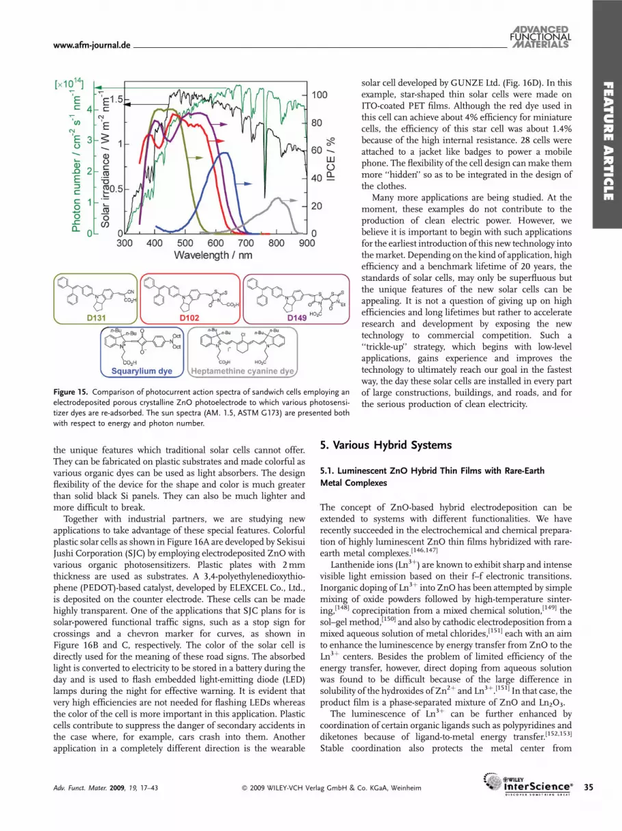
FEATUREARTIC
LE
www.afm-journal.de
Figure 15. Comparison of photocurrent action spectra of sandwich cells employing an
electrodeposited porous crystalline ZnO photoelectrode to which various photosensi-
tizer dyes are re-adsorbed. The sun spectra (AM. 1.5, ASTM G173) are presented both
with respect to energy and photon number.
the unique features which traditional solar cells cannot offer.They can be fabricated on plastic substrates and made colorful asvarious organic dyes can be used as light absorbers. The designflexibility of the device for the shape and color is much greaterthan solid black Si panels. They can also be much lighter andmore difficult to break.
Together with industrial partners, we are studying newapplications to take advantage of these special features. Colorfulplastic solar cells as shown in Figure 16A are developed by SekisuiJushi Corporation (SJC) by employing electrodeposited ZnO withvarious organic photosensitizers. Plastic plates with 2mmthickness are used as substrates. A 3,4-polyethylenedioxythio-phene (PEDOT)-based catalyst, developed by ELEXCEL Co., Ltd.,is deposited on the counter electrode. These cells can be madehighly transparent. One of the applications that SJC plans for issolar-powered functional traffic signs, such as a stop sign forcrossings and a chevron marker for curves, as shown inFigure 16B and C, respectively. The color of the solar cell isdirectly used for the meaning of these road signs. The absorbedlight is converted to electricity to be stored in a battery during theday and is used to flash embedded light-emitting diode (LED)lamps during the night for effective warning. It is evident thatvery high efficiencies are not needed for flashing LEDs whereasthe color of the cell is more important in this application. Plasticcells contribute to suppress the danger of secondary accidents inthe case where, for example, cars crash into them. Anotherapplication in a completely different direction is the wearable
Adv. Funct. Mater. 2009, 19, 17–43 � 2009 WILEY-VCH Verlag GmbH & C
solar cell developed by GUNZE Ltd. (Fig. 16D). In thisexample, star-shaped thin solar cells were made onITO-coated PET films. Although the red dye used inthis cell can achieve about 4% efficiency for miniaturecells, the efficiency of this star cell was about 1.4%because of the high internal resistance. 28 cells wereattached to a jacket like badges to power a mobilephone. The flexibility of the cell design can make themmore ‘‘hidden’’ so as to be integrated in the design ofthe clothes.
Many more applications are being studied. At themoment, these examples do not contribute to theproduction of clean electric power. However, webelieve it is important to begin with such applicationsfor the earliest introduction of this new technology intothemarket. Depending on the kind of application, highefficiency and a benchmark lifetime of 20 years, thestandards of solar cells, may only be superfluous butthe unique features of the new solar cells can beappealing. It is not a question of giving up on highefficiencies and long lifetimes but rather to accelerateresearch and development by exposing the newtechnology to commercial competition. Such a‘‘trickle-up’’ strategy, which begins with low-levelapplications, gains experience and improves thetechnology to ultimately reach our goal in the fastestway, the day these solar cells are installed in every partof large constructions, buildings, and roads, and forthe serious production of clean electricity.
5. Various Hybrid Systems
5.1. Luminescent ZnO Hybrid Thin Films with Rare-Earth
Metal Complexes
The concept of ZnO-based hybrid electrodeposition can beextended to systems with different functionalities. We haverecently succeeded in the electrochemical and chemical prepara-tion of highly luminescent ZnO thin films hybridized with rare-earth metal complexes.[146,147]
Lanthenide ions (Ln3þ) are known to exhibit sharp and intensevisible light emission based on their f–f electronic transitions.Inorganic doping of Ln3þ into ZnO has been attempted by simplemixing of oxide powders followed by high-temperature sinter-ing,[148] coprecipitation from a mixed chemical solution,[149] thesol–gel method,[150] and also by cathodic electrodeposition from amixed aqueous solution of metal chlorides,[151] each with an aimto enhance the luminescence by energy transfer from ZnO to theLn3þ centers. Besides the problem of limited efficiency of theenergy transfer, however, direct doping from aqueous solutionwas found to be difficult because of the large difference insolubility of the hydroxides of Zn2þ and Ln3þ.[151] In that case, theproduct film is a phase-separated mixture of ZnO and Ln2O3.
The luminescence of Ln3þ can be further enhanced bycoordination of certain organic ligands such as polypyridines anddiketones because of ligand-to-metal energy transfer.[152,153]
Stable coordination also protects the metal center from
o. KGaA, Weinheim 35
FEATUREARTIC
LE
www.afm-journal.de
Figure 16. Various unique applications of colorful plastic solar cells
employing electrodeposited ZnO photoelectrodes. Fully plastic solar cells
employing many color variations and shapes, as developed by Sekisui Jushi
Corporation, Japan (A). These cells are made with 2mm thick hard plastic
electrodes. The counter electrode employs 3,4-polyethylenedioxythiophene
(PEDOT) as catalyst (developed by ELEXCEL Co., Ltd., Japan). Sekisui Jushi
Corporation is developing self-powered traffic signs by assembling these
plastic cells into modules, such as B) a stop sign in Japan and C) a chevron
marker for curves. The red color of the cells are used for the meaning of the
road signs and the electricity generated is to be stored during the day and
used to flash embedded light-emitting diode (LED) lights during the night
to warn the drivers. Because the signs are made of plastic, they further
ensure safety by reducing the risk of a secondary accident in the case where
a car crashes into them. The picture in (D) shows a prototype of a wearable
solar cell developed by GUNZE Ltd., Japan. Star-shaped, red-colored, and
light-weight thin plastic solar cells are fabricated by employing ITO-coated
polyethyleneterephthalete (PET) films, and 28 cells are attached to a jacket
and wired to a small DC–DC converter in the jacket to feed a mobile phone.
The difference from other existing concepts of solar-cell installation to
clothes is that one can design the shape and color of the solar cells to fit to
the design of the cloth, instead of matching design of cloth to hard and
black Si panels.
36 � 2009 WILEY-VCH Verlag GmbH
coordination by water molecules, which significantly weaken theluminescence. Our idea then was to try to introduce Ln3þ in theform of such complexes to ZnO, rather than doping itinorganically. The dcbpy ligand was thought as a suitablecandidate for such a purpose. Dcbpy is actually a ligand in the Rucomplex photosensitizer in DSSCs, with its nitrogen atomscoordinating to Ru2þ and its carboxylates to TiO2.
[50] Thecarboxylic acid function in fact coordinates to Ln3þ to formstable complexes.[154] Therefore, synthesis of a Ln3þ complex withdcbpy and its addition to the bath for electrodeposition of ZnO didnot result in loading of the complex into ZnO. However, thestrategy as shown in Figure 17 gave us successful results.
Dcbpy was simply added at concentrations up to 200mM intothe bath containing ZnCl2. Cathodic electrolysis yielded a whitethin film with a highly porous structure, as shown in Figure 17.Loading of dcbpy molecules in a high amount was confirmedboth by FTIR and UV absorption spectra.[146] During theelectrodeposition, dcbpy molecules are expected to stick to theZnO surface through their carboxylic acid groups. The resultantZnO/dcbpy hybrid thin film was then simply soaked in anethanolic solution of LnCl3. When it is activated with EuCl3,intense red-light emission was observed by excitation of the filmwith UV light. The emission spectrum showed the most intensepeak at 613 nm along with several other peaks, which arecharacteristic of Eu3þ complexes.[146] When TbCl3 is used, greenemission occurred as a result of the formation of Tb3þ complexes.The uptake of Ln3þ ions by coordination of surface-bound dcbpymolecules through their nitrogen atoms is evident; that is, dcbpycan be regarded as a bridging ligand to couple ZnO with Ln3þ
ions. Luminescent hybrid thin films can also be obtained byelectrodepositing porous ZnO using eosinY as is done for solarcells and subsequently adsorbing dcbpy.[147] Because of the highsurface area of eosinY-templated porous ZnO, dcbpy can beadsorbed in a large amount and the adsorbed dcbpy moleculespick up Ln3þ ions.
The photoluminescence could be significantly enhanced andstabilized by further dipping the ZnO/dcbpy/Eu3þ film intoa solution of 4,4,4-trifluoro-1-(2-thienyl)-1,3-butanedione-2-thenoyltrifluoroacetone (TTA). The TTA molecules are expectedto coordinate to Eu3þ centers to cap the complex againstcoordination of water molecules. Without capping, the photo-luminescence gradually decayed when the film was stored inmoist air for a fewweeks. The luminescence of the capped film, incontrast, did not change at all. The excitation spectrum of such ahybrid film indicated the features of both dcbpy and TTA, whichconfirms efficient energy transfer from these ligands. Thequantum efficiency of photoluminescence was around 20% atroom temperature.
The future of this luminescent hybrid material is verypromising in many applications. One of the most exciting fieldscan be found in the construction of hybrid electroluminescentdevices for lighting and display purposes. The traditionalinorganic electroluminescent devices and organic light-emittingdiodes (OLEDs) can be regarded as devices that function inverselyof inorganic solar cells and organic p–n heterojuction solar cells,respectively. Then, the hybrid electroluminescent device can beregarded as a version of solid-state DSSCs.[155–159] Instead ofshining light to output electricity, electricity is fed into the deviceto obtain light. The luminescent molecules are attached to ZnO,
& Co. KGaA, Weinheim Adv. Funct. Mater. 2009, 19, 17–43

FEATUREARTIC
LE
www.afm-journal.de
Figure 17. Electrodeposition of luminescent ZnO/rare earth metal complex hybrid thin films; graphical
presentations of expected reactions and pictures of the products are shown. The goal is to develop a
hybrid electroluminescent device, in which electrodeposited inorganic semiconductors serve as charge
carriers while organometallic molecules act as luminescent centers.
Adv. Funct. Mater. 2009, 19, 17–43 � 2009 WILEY-VCH Verlag GmbH & Co. KGaA, Weinhei
which is a very good electron conductor.As a hole conductor, CuSCN can beinteresting as it is a wide-bandgap p-type semiconductor and can be electro-deposited from solution.[158,159] Thedifficulty is how to fill up the nanoporesof ZnO with such a solid mate-rial.[156,157] Having succeeded in fabri-cating such hybrid electroluminescentdevices, the clear advantage is that theprocess permits use of plastic substratesand the material is fairly stable in moistair unlike the materials used in OLEDs.It should also be beneficial that thecharge carriers are inorganic semicon-ductors with high carrier mobilities,and light-emitting centers are theorganometallic molecules with highefficiency and color selectivity of lumi-nescence. Plastic and full-color light-emitting devices with large area and lowcost will be the goal of the study.
5.2. p-CuSCN/Dye Hybrid Thin
Films
As noted in the previous section,CuSCN is a wide-bandgap p-type semi-conductor and can be cathodicallyelectrodeposited from solutions con-taining SCN� and Cu2þ ions accordingto the following reaction:[158,159]
Cu2þ þ SCN� þ e� ! CuSCN (17)
although details of the deposition
mechanism have not been clarified
yet. O’Regan et al. employed this
reaction to fabricate solid-state DSSCs.
However, complete filling of nanopores
of dye-sensitized TiO2 and ZnO photo-
anodes turned out to be difficult and
they later improved the efficiency by
simply casting a solution of CuSCN in
propyl sulfide.[157] p-CuI is also a
compound semiconductor that was
frequently used as a hole conductor in
solid-state DSSCs.[155,156] Charge
separation in such devices is expected
to occur at the triple interfaces such as
TiO2/dye/CuSCN and TiO2/dye/CuI.
Electrons injected from the dye travel
through the network of TiO2, while
holes are transferred to the p-type
semiconductors and travel through
them. The importance of chemical
m 37
FEATUREARTIC
LE
www.afm-journal.de
38
binding of dye molecules to the surface of n-type semiconductors
for efficient electron injection is well-known. However, not much
is known about the chemistry between dyes and the p-type
materials in such devices. Are the dye molecules bound to
CuSCN and is such binding important for the cell to work?In fact, there have been a few studies on cathodic dye-
sensitization of p-type semiconductor electrodes such asCuSCN[160,161] and NiO.[162] Even though their output was verysmall, these examples already show that certain dye moleculescan be bound to the surface of these compounds and inject holesfrom the photoexcited states. We therefore attempted cathodicelectrodeposition of hybrid thin films of CuSCN and dyes.[163]
The question is which dye to use. Carboxylic acid is the typicalanchor to TiO2 and we have experienced the same for ZnO.Sulfonates and phosphonates are also used. From the traditionalclassification of coordination chemistry, TiIV sites of TiO2 act astypical hard Lewis acids, and hard Lewis bases of carboxylate,sulfonate, and phosphonate groups should form stable bonds. Onthe contrary, the CuI sites of CuSCN are typical soft Lewis acids.According to the HSAB (hard and soft, acid and base) principle,soft Lewis basic groups should be the suitable anchor to CuSCN.Sulfur-containing substituents such as –SH and –NCS areexpected to behave as soft Lewis bases. We have searched forcommercial dye molecules with such functions and only found afew. Fluorescein isothiocyanate is a xanthene dye with –NCS andthe famous Ru complex photosensitizer Ru(dcbpy)2(NCS)2 alsohappens to have the –NCS group. We have performedelectrodeposition of CuSCN thin films in the presence of thesedyes and also with eosinY for comparison, the latter dye onlyhaving a carboxylic acid group that binds very well to ZnO.
The results were very clear and interesting. EosinY was notloaded into CuSCN at all, while the other two dyes with the –NCSgroup were loaded into the film. Figure 18 shows variation ofsurface morphology of the films. The CuSCN thin film withoutdye is colorless and consists of rugged particles. Almost the samecolorless thin film was obtained in the presence of eosinY and itsmorphology is unchanged. XRD patterns of these two filmsindicate peaks of randomly oriented well-crystallized CuSCN. It isevident that the carboxylated eosinY molecule does not bind toCuSCN and therefore does not influence its crystal growth. Both–NCS-containing dyes yielded colored hybrid thin films, orangefor fluorescein isothiocyanate and brown for Ru(dcbpy)2(NCS)2.Very interesting is the fact that these hybrid thin films have verysimilar morphology, which is totally different from the pureCuSCN, showing hexagonal edges of the particles and thepresence of an internal nanostructure. The XRD patterns of thesefilms indicate preferential orientation of crystallites, with the c-axis of rhombohedral CuSCN perpendicular to the substrate.[163]
It is now apparent that the –NCS group does coordinate to thesurface of CuSCN and makes it possible to obtain hybrid thinfilms by codeposition.
Absorption spectra of the CuSCN hybrid thin films withfluorescein isothiocyanate and Ru(dcbpy)2(NCS)2 are comparedto that of the pure CuSCN in Figure 19. Loading of the dyemolecules is obvious from the characteristic absorption in thevisible range. Photoelectrochemical analysis was performed in athree-electrode setup employing the hybrid thin films as workingelectrode. The problem in such studies is that there is no suitable
� 2009 WILEY-VCH Verlag GmbH
redox electrolyte system.[160] When methyl viologen was used asan electron acceptor, a photocathodic current of about 0.1 and0.2mAcm�2 was observed for fluorescein isothiocyanate andRu(dcbpy)2(NCS)2 hybrid thin films, respectively, under illumi-nation with AM 1.5 simulated sunlight from the side of the backcontact.[163] The photocurrent action spectrum measured for theCuSCN/Ru(dcbpy)2(NCS)2 hybrid thin film clearly indicatesphotosensitization by the dye (Fig. 19). The maximum IPCE of5.4% was reached around the absorption peak of the dye. Thelimited efficiency can be attributed to the inefficient electrontransfer from the dye to methyl viologen as much of the loadeddyes seem to be inaccessible from the electrolyte solution.Because only photocathodic current was observed even whenreversible redox systems such as [Fe(CN)6]
3�/4� and Sn2þ/4þ
were used as the electrolyte, hole injection from the photoexcitedstate of the dye to the valence band of CuSCN was evident.
Construction of highly efficient solar cells based on these dye-sensitized photocathodes may be difficult because the voltage ofsuch cells is also low (ca. 100mV) partly because of theunmatched potential of the redox system. However, these studiesevinced the importance of chemical bond formation at theCuSCN/dye interface. The influence of dye addition to the crystalgrowth of CuSCN found in the present example certainlydeserves full investigations to clarify the mechanism of hybridformation. Further information about the suitable design of theanchoring group can be obtained through such studies forimprovement of solid-state DSSCs and new properties of thesehybrid materials can also be anticipated.
5.3. Anodic Electrodeposition of a Titanate/Quinone Hybrid
Thin Film
Electrodeposition of inorganic/organic hybrid thin films can alsobe performed as an anodic process. Thin films of metal oxidesthat are typically electrically insulating can be obtained by meansof anodic hybrid electrodeposition with benzoquinone.[164]
Electrodeposition of TiO2 thin films has been tried by severaldifferent approaches because of the usefulness of the material.Kavan et al. have proposed anodic oxidation of TiIII to deposit TiIV
species from an aqueous solution of TiCl3,[165] while Natarajan
et al. have employed cathodic reduction of nitrate ions in an acidicsolution of TiIV peroxo complex to precipitate TiIV species by pHchange.[83] In both of these cases, however, the thin filmsprimarily obtained were insulating amorphous solid of TiIV
hydroxides, so that the achievable film thickness was limited and/or thin films with a porous structure could only be obtained.[84]
These films then need to be heated at high temperatures tocrystallize into TiO2. Wessels et al. recently observed directcrystallization of TiO2 by modification of Kavan’s methodemploying surfactants, although nanometer-sized crystals couldonly be obtained.[166]
Stable aqueous solutions are rare for high-valence metalcations like Ti4þ because of the facile formation of metastablehydroxides. Aqueous solutions are therefore obtained only inhighly acidic environments. Ohya et al. have discovered a methodto prepare a stable basic aqueous solution of titanate electro-statically stabilized by bulky alkylammonium cations.[167] When
& Co. KGaA, Weinheim Adv. Funct. Mater. 2009, 19, 17–43
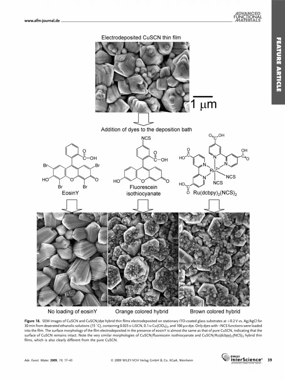
FEATUREARTIC
LE
www.afm-journal.de
Figure 18. SEM images of CuSCN and CuSCN/dye hybrid thin films electrodeposited on stationary ITO-coated glass substrates atþ0.2 V vs. Ag/AgCl for
30min from deaerated ethanolic solutions (15 8C), containing 0.025M LiSCN, 0.1 M Cu(ClO4)2, and 100mM dye. Only dyes with –NCS functions were loaded
into the film. The surface morphology of the film electrodeposited in the presence of eosinY is almost the same as that of pure CuSCN, indicating that the
surface of CuSCN remains intact. Note the very similar morphologies of CuSCN/fluorescein isothiocyanate and CuSCN/Ru(dcbpy)2(NCS)2 hybrid thin
films, which is also clearly different from the pure CuSCN.
Adv. Funct. Mater. 2009, 19, 17–43 � 2009 WILEY-VCH Verlag GmbH & Co. KGaA, Weinheim 39
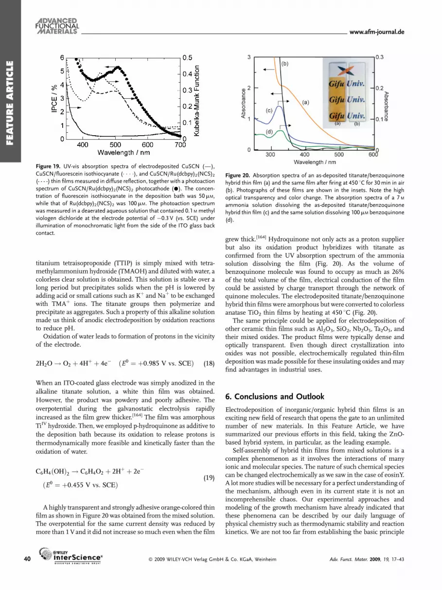
FEATUREARTIC
LE
www.afm-journal.de
Figure 19. UV-vis absorption spectra of electrodeposited CuSCN (—),
CuSCN/fluorescein isothiocyanate (� � � �), and CuSCN/Ru(dcbpy)2(NCS)2(- - - -) thin filmsmeasured in diffuse reflection, together with a photoaction
spectrum of CuSCN/Ru(dcbpy)2(NCS)2 photocathode (�). The concen-
tration of fluorescein isothiocyanate in the deposition bath was 50mM,
while that of Ru(dcbpy)2(NCS)2 was 100mM. The photoaction spectrum
was measured in a deaerated aqueous solution that contained 0.1 M methyl
viologen dichloride at the electrode potential of �0.3 V (vs. SCE) under
illumination of monochromatic light from the side of the ITO glass back
contact.
Figure 20. Absorption spectra of an as-deposited titanate/benzoquinone
hybrid thin film (a) and the same film after firing at 450 8C for 30min in air
(b). Photographs of these films are shown in the insets. Note the high
optical transparency and color change. The absorption spectra of a 7 M
ammonia solution dissolving the as-deposited titanate/benzoquinone
hybrid thin film (c) and the same solution dissolving 100mM benzoquinone
(d).
40
titanium tetraisopropoxide (TTIP) is simply mixed with tetra-methylammonium hydroxide (TMAOH) and diluted with water, acolorless clear solution is obtained. This solution is stable over along period but precipitates solids when the pH is lowered byadding acid or small cations such as Kþ and Naþ to be exchangedwith TMAþ ions. The titanate groups then polymerize andprecipitate as aggregates. Such a property of this alkaline solutionmade us think of anodic electrodeposition by oxidation reactionsto reduce pH.
Oxidation of water leads to formation of protons in the vicinityof the electrode.
2H2O ! O2 þ 4Hþ þ 4e� ðE0 ¼ þ0:985 V vs: SCEÞ (18)
When an ITO-coated glass electrode was simply anodized in the
alkaline titanate solution, a white thin film was obtained.
However, the product was powdery and poorly adhesive. The
overpotential during the galvanostatic electrolysis rapidly
increased as the film grew thicker.[164] The film was amorphous
TiIV hydroxide. Then, we employed p-hydroquinone as additive to
the deposition bath because its oxidation to release protons is
thermodynamically more feasible and kinetically faster than the
oxidation of water.
C6H4ðOHÞ2 ! C6H4O2 þ 2Hþ þ 2e�
ðE0 ¼ þ0:455 V vs: SCEÞ(19)
A highly transparent and strongly adhesive orange-colored thinfilm as shown in Figure 20 was obtained from themixed solution.The overpotential for the same current density was reduced bymore than 1Vand it did not increase so much even when the film
� 2009 WILEY-VCH Verlag GmbH
grew thick.[164] Hydroquinone not only acts as a proton supplierbut also its oxidation product hybridizes with titanate asconfirmed from the UV absorption spectrum of the ammoniasolution dissolving the film (Fig. 20). As the volume ofbenzoquinone molecule was found to occupy as much as 26%of the total volume of the film, electrical conduction of the filmcould be assisted by charge transport through the network ofquinone molecules. The electrodeposited titanate/benzoquinonehybrid thin films were amorphous but were converted to colorlessanatase TiO2 thin films by heating at 450 8C (Fig. 20).
The same principle could be applied for electrodeposition ofother ceramic thin films such as Al2O3, SiO2, Nb2O5, Ta2O5, andtheir mixed oxides. The product films were typically dense andoptically transparent. Even though direct crystallization intooxides was not possible, electrochemically regulated thin-filmdeposition wasmade possible for these insulating oxides andmayfind advantages in industrial uses.
6. Conclusions and Outlook
Electrodeposition of inorganic/organic hybrid thin films is anexciting new field of research that opens the gate to an unlimitednumber of new materials. In this Feature Article, we havesummarized our previous efforts in this field, taking the ZnO-based hybrid system, in particular, as the leading example.
Self-assembly of hybrid thin films from mixed solutions is acomplex phenomenon as it involves the interactions of manyionic and molecular species. The nature of such chemical speciescan be changed electrochemically as we saw in the case of eosinY.A lot more studies will be necessary for a perfect understanding ofthe mechanism, although even in its current state it is not anincomprehensible chaos. Our experimental approaches andmodeling of the growth mechanism have already indicated thatthese phenomena can be described by our daily language ofphysical chemistry such as thermodynamic stability and reactionkinetics. We are not too far from establishing the basic principle
& Co. KGaA, Weinheim Adv. Funct. Mater. 2009, 19, 17–43
FEATUREARTIC
LE
www.afm-journal.de
by which we can resolve the complex phenomena into severalmajor factors, analyze and reintegrate them into one picture todescribe the hybrid film growth. Even though it is highlydemanding work, we should remember that the complexity ofsuch mixed systems is precisely the reason for its potential use todiscover many new materials.
We have also reviewed and discussed the usefulness of thehybrid materials. The plastic DSSCs may become the firstexample of an industrial application of electrodeposited ZnO-based hybrid thin films. Further advanced applications such aslight-emitting devices can also be envisaged. What makes thesenew materials truly interesting and useful to us is that theelectrochemical process is inherently very simple and econom-ical, easily scalable formass production, unlike the correspondingphysical methods, which need high energy and expensiveequipment to handle high vacuum and temperature. Hybridelectrodeposition is simply difficult to understand, and therebywe are, as yet, not able to take full control of it. That is the verychallenge and task given to us as researchers.
Acknowledgements
The present work has received financial support from the following sources:IncorporatedAdministrative Agency,NewEnergy and Industrial TechnologyDevelopmentOrganization (NEDO) (01B64002c, 06A22002d, 06002295-0)under theMinistryof theEconomy, Tradeand Industryof Japan;Grant-in-Aidfor Scientific Research (15681005, 15655047); Nanotechnology SupportProgram of the Ministry of Education, Culture, Sports, Science, andTechnology of Japan. The authors are grateful to Prof. L. M. Peter of theUniversity of Bath for discussion on the photoelectrochemical properties ofelectrodeposited ZnO/dye hybrid cells. Supporting Information is availableonline from Wiley Interscience or from the author.
Received: February 13, 2007
Revised: February 25, 2008
Published online: December 4, 2008
[1] M. Datta, Electrochim. Acta 2003, 48, 2975.
[2] T. P. Moffat, D. Wheeler, S.-K. Kim, D. Josell, J. Electrochem. Soc. 2006, 153,
C127.
[3] L. Sergey, Rec. Res. Dev. Electrochem. 2003, 6, 57.
[4] A. S. Baranski, W. R. Fawcett, A. C. McDonald, R. M. Nobriga, J. R.
MacDonald, J. Electrochem. Soc. 1981, 128, 963.
[5] G. P. Power, D. R. Peggs, A. Parker, Electrochim. Acta 1981, 26, 681.
[6] I. Kaur, D. K. Pandya, K. L. Chopra, J. Electrochem. Soc. 1980, 127, 943.
[7] D. Lincot, R. Ortega Borges, J. Electrochem. Soc. 1992, 139, 1880.
[8] R. Ortega Borges, D. Lincot, J. Electrochem. Soc. 1993, 140, 3464.
[9] P. C. Rieke, S. B. Bentjen, Chem. Mater. 1993, 5, 43.
[10] J. M. Dona, J. Herrero, J. Electrochem. Soc. 1997, 144, 4081.
[11] K. Yamaguchi, T. Yoshida, T. Sugiura, H. Minoura, J. Phys Chem. B 1998,
102, 9677.
[12] K. Yamaguchi, T. Yoshida, D. Lincot, H. Minoura, J. Phys. Chem. B 2003,
107, 387.
[13] T. Yoshida, K. Yamaguchi, T. Kazitani, T. Sugiura, H. Minoura, J.
Electroanal. Chem. 1999, 473, 209.
[14] G. Hodes, Physical Electrochemistry: Principles, Methods, Applications (Ed: I.
Rubinstein), Marcel Dekker, New York 1995, Ch. 12.
[15] M. Froment, M. Claude Bernard, R. Cortes, B. Mokili, D. Lincot, J.
Electrochem. Soc. 1995, 142, 2642.
Adv. Funct. Mater. 2009, 19, 17–43 � 2009 WILEY-VCH Verl
[16] M. Froment, D. Lincot, Electrochim. Acta 1995, 40, 1293.
[17] G. Hodes, Y. Golan, D. Behar, Y. Zhang, B. Alperson, I. Rubinstein,
Nanoparticles and Nanostructured Films (Ed: J.H. Fendler), Wiley-VCH,
Weinheim, Germany 1998, Ch. 1.
[18] J. A. Switzer, Nanoparticles and Nanostructured Films (Ed: J.H. Fendler),
Wiley-VCH, Weinheim, Germany 1998, Ch. 3.
[19] D. Lincot, M. Froment, H. Cachet, Advances in Electrochemical Science and
Engineering, Vol. 6(Eds: R. C. Alkire, D. M. Kolb), Wiley-VCH, Weinheim,
Germany 1999, pp. 165–235.
[20] M. J. Furlong, M. Froment, M. C. Bernard, R. Cortes, A. N. Tiwari, M.
Krejci, H. Zogg, D. Lincot, J. Cryst. Growth 1998, 193, 114.
[21] L. Stolt, J. Hedstrom, J. Kessler, M. Ruckh, K.-O. Velthaus, H. W. Schock,
Appl. Phys. Lett. 1993, 62, 597.
[22] L. Kronik, L. Burstein, M. Leibovitch, Y. Shapira, D. Gal, E. Moons, J. Beier,
G. Hodes, D. Cahen, D. Hariskos, R. Klenk, H.-W. Schock, Appl. Phys. Lett.
1995, 67, 1405.
[23] N. W. Duffy, D. Lane, M. E. Ozsan, L. M. Peter, K. D. Rogers, R. L. Wang,
Thin Solid Films 2000, 361/362, 314.
[24] A. Kampmann, V. Sittinger, J. Rechid, R. Reineke-Koch, Thin Solid Films
2000, 361/362, 309.
[25] M. C. Chang, W. H. Douglas, J. Tanaka, J. Mater. Sci. Mater. Med. 2006, 17,
387.
[26] M. Catauro, M. G. Raucci, D. De Marco, L. Ambriosio, J. Biomed. Mater.
Res. A 2006, 77A, 340.
[27] A. Oki, X. Qiu, O. Alawode, B. Foley, Mater. Lett. 2006, 60, 2751.
[28] P. P. Lima, S. A. Junior, O. L. Malta, L. D. Carlos, R. A. Sa Ferreira, R.
Pavithran, M. L. P. Reddy, Eur. J. Inorg. Chem. 2006, 3923.
[29] A. D. Pomogailo, Colloid J. 2005, 67, 658.
[30] B. Yan, R.-F. Yao, Q.-M. Wang, Mater. Lett. 2006, 60, 3063.
[31] M. Lira-Cantu, P. Gomez-Romero, Chem. Mater. 1998, 10, 698.
[32] M. A. Petruska, D. R. Talham, Chem. Mater. 1998, 10, 3672.
[33] E. Coronado, C. Mingotaud, Adv. Mater. 1999, 11, 869.
[34] V. Monnier, N. Sanz, E. Botzung-Appert, M. Bacia, A. Ibanez, J. Mater.
Chem. 2006, 16, 1401.
[35] K. Moller, T. Bein, Chem. Mater. 1998, 10, 2950.
[36] G. Calzaferri, S. Huber, H. Maas, C. Minkowski, Angew. Chem., Int. Ed.
2003, 42, 3732.
[37] T. Tani, Nippon Shashin Gakkaishi 1971, 34, 1.
[38] S. Daehne, J. Photograph. Sci. 1990, 38, 66.
[39] Z. Zhu, Dyes Pigm. 1995, 27, 77.
[40] B. O’Regan, M. Gratzel, Nature 1991, 353, 737.
[41] H. Gerischer, H. Tributsch, Ber. Bunsen-Ges. Physik. Chem. 1968, 72, 437.
[42] H. Gerischer, Photochem. Photobiol. 1972, 16, 243.
[43] H. Tsubomura, M. Matsumura, Y. Nomura, T. Amemiya, Nature 1976,
261, 402.
[44] M. Matsumura, S. Matsudaira, H. Tsubomura, M. Tanaka, H. Yanagida,
Ind. Eng. Chem. Prod. Res. Dev. 1980, 19, 415.
[45] S. Anderson, E. C. Constable, M. P. Dare-Edwards, J. B. Goodenough, A.
Hamnett, K. R. Seddon, R. D. Wright, Nature 1979, 280, 571.
[46] M. Gratzel, J. Photochem. Photobiol. A 2004, 164, 3.
[47] L. M. Peter, N. W. Duffy, R. L. Wang, K. G. U. Wijayantha, J. Electroanal.
Chem. 2002, 524/525, 127.
[48] A. J. Frank, N. Kopidakis, J. van de Lagemaat, Coord. Chem. Rev. 2004, 248,
1165.
[49] J. Nelson, R. E. Chandler, Coord. Chem. Rev. 2004, 248, 181.
[50] M. K. Nazeeruddin, A. Kay, I. Rodicio, R. Humphry-Baker, E. Muller, P.
Liska, N. Valchopoulos, M. Gratzel, J. Am. Chem. Soc. 1993, 115,
6382.
[51] M. Gratzel, Prog. Photovoltaics 2006, 16, 429.
[52] N. Koide, A. Islam, Y. Chiba, L. Han, J. Photochem. Photobiol. A 2006, 182,
296.
[53] N. G. Park, G. Schlichthorl, J. van de Lagemaat, H. M. Cheong, A.
Mascarenhas, A. J. Frank, J. Phys. Chem. B 1999, 103, 3308.
[54] F. Pichot, J. R. Pitts, B. A. Gress, Langmuir 2000, 16, 5626.
ag GmbH & Co. KGaA, Weinheim 41

FEATUREARTIC
LE
www.afm-journal.de
42
[55] S. Nakade, M. Matsuda, S. Kambe, Y. Saito, T. Kitamura, T. Sakata, Y.
Wada, H. Mori, S. Yanagida, J. Phys. Chem. B 2002, 106(39), 10004.
[56] T. Miyasaka, Y. Kijitori, J. Electrochem. Soc. 2004, 151, A1767.
[57] H. Lindstrom, A. Holmberg, E. Magnusson, S.-E. Lindquist, L. Malmqvist,
A. Hagfeldt, Nano Lett. 2001, 1, 97.
[58] S. A. Haque, E. Palomares, H. M. Upadhyaya, L. Otley, R. J. Potter, A. B.
Holmes, J. R. Durrant, Chem. Commun. 2003, 3008.
[59] S. Uchida, M. Tomiha, T. Hirotsugu, M. Kawaraya, J. Photochem.
Photobiol. A 2004, 164, 93.
[60] D. Zhang, T. Yoshida, H. Minoura, Adv. Mater. 2003, 15, 814.
[61] D. Zhang, T. Yoshida, K. Furuta, H. Minoura, J. Photochem. Photobiol. A
2004, 164, 159.
[62] T. Oekermann, D. Zhang, T. Yoshida, H. Minoura, J. Phys. Chem. B 2004,
108, 2227.
[63] T. N. Murakami, Y. Kijitori, N. Kawashima, T. Miyasaka, J. Photochem.
Photobiol. A 2004, 164, 187.
[64] D. Zhang, T. Yoshida, T. Oekermann, K. Furuta, H. Minoura, Adv. Funct.
Mater. 2006, 16, 1228.
[65] D. C. Look, Mater. Sci. Eng. 2001, B80, 383.
[66] E. Bellingeri, D. Marre, L. Pellegrino, I. Pallecchi, G. Canu, M. Vignolo, C.
Bernini, A. S. Siri, Superlattices Microstruct. 2005, 38, 446.
[67] T. Minami, Semicond. Sci. Technol. 2005, 20, S35.
[68] N. G. Dhere, Sol. Energy Mater. Sol. Cells 2006, 90, 2181.
[69] M. Izaki, T. Omi, Appl. Phys. Lett 1996, 68, 2439.
[70] M. Izaki, T. Omi, J. Electrochem. Soc. 1996, 143, L53.
[71] S. Peulon, D. Lincot, Adv. Mater. 1996, 8, 166.
[72] S. Peulon, D. Lincot, J. Electrochem. Soc. 1998, 145, 864.
[73] T. Pauporte, D. Lincot, J. Electrochem. Soc. 2001, 148, C310.
[74] T. Pauporte, D. Lincot, J. Electroanal. Chem. 2001, 517, 54.
[75] J. A. Cox, A. Brajter, Electrochim. Acta 1979, 24, 517.
[76] N. Ogawa, H. Kodaiku, S. Ikeda, J. Electroanal. Chem. 1986, 208, 117.
[77] N. Ogawa, S. Ikeda, Anal. Sci. Suppl. 1991, 7, 1681.
[78] T. Yoshida, D. Komatsu, N. Shimokawa, H. Minoura, Thin Solid Films
2004, 451/452, 166.
[79] D. Tench, L. F. Warren, J. Electrochem. Soc. 1983, 130, 869.
[80] S. Sawatani, S. Ogawa, T. Yamada, M. Kamiya, T. Yoshida, H. Minoura,
Trans. Mater. Res. Soc. Jpn. 2003, 28, 381.
[81] A. Seshadri, N. R. de Tacconi, C. R. Chenthamarakshan, K. Rajeshwar,
Electrochem. Solid-State Lett. 2006, 9, C1.
[82] L. Gal-Or, I. Silberman, R. Chaim, J. Electrochem. Soc. 1991, 138, 1939.
[83] C. Natarajan, G. Nogami, J. Electrochem. Soc. 1996, 143, 1547.
[84] S. Karuppuchamy, D. P. Amalnerkar, K. Yamaguchi, T. Yoshida, T. Sugiura,
H. Minoura, Chem. Lett. 2001, 30, 78.
[85] H. Minoura, K. Naruto, H. Takano, E. Haseo, T. Sugiura, Y. Ueno, T. Endo,
Chem Lett. 1991, 379.
[86] Y. Matsumoto, H. Adachi, J. Hombo, J. Am. Ceram. Soc. 1993, 76, 769.
[87] S. T. Chang, I. C. Leu, M. H. Hon, Electrochem. Solid-State Lett. 2002, 5,
C71.
[88] R. Schrebler, K. Bello, F. Vera, P. Cury, E. Munoz, R. Del Rıo, H. Gomez
Meier, R. Cordova, E. A. Dalchiele, Electrochem. Solid-State Lett. 2006, 9,
C110.
[89] T. Pauporte, D. Lincot, Appl. Phys. Lett. 1999, 75, 24.
[90] T. Pauporte, R. Cortes, M. Froment, B. Beaumont, D. Lincot, Chem.Mater.
2002, 14, 4702.
[91] S. J. Limmer, E. A. Kulp, J. A. Switzer, Langmuir 2006, 22, 10 535.
[92] T. Yoshida, K. Miyamoto, N. Hibi, T. Sugiura, H. Minoura, D. Schlettwein,
T. Oekermann, G. Schneider, D. Wohrle, Chem. Lett. 1998, 27, 599.
[93] D. Schlettwein, T. Oekermann, T. Yoshida, M. Tochimoto, H. Minoura, J.
Electroanal. Chem. 2000, 481, 42.
[94] T. Oekermann, T. Yoshida, D. Schlettwein, T. Sugiura, H. Minoura, Phys.
Chem. Chem. Phys. 2001, 3, 3387.
[95] T. Yoshida, M. Tochimoto, D. Schlettwein, D. Wohrle, T. Sugiura, H.
Minoura, Chem. Mater. 1999, 11, 2657.
[96] T. Yoshida, H. Minoura, Adv. Mater. 2000, 12, 1219.
� 2009 WILEY-VCH Verlag GmbH
[97] T. Yoshida, S. Ide, T. Sugiura, H. Minoura, Trans. Mater. Res. Soc. Jpn.
2000, 25, 1111.
[98] T. Yoshida, J. Yoshimura, M.Matsui, T. Sugiura, H. Minoura, Trans. Mater.
Res. Soc. Jpn. 1999, 24, 497.
[99] S. Karuppuchamy, T. Yoshida, T. Sugiura, H. Minoura, Thin Solid Films
2001, 397, 63.
[100] T. Oekermann, S. Karuppuchamy, T. Yoshida, D. Schlettwein, D. Wohrle,
H. Minoura, J. Electrochem. Soc. 2004, 151, C62.
[101] E. Michaelis, K. Nonomura, D. Schlettwein, T. Yoshida, H. Minoura, D.
Wohrle, J. Porphyrins Phthalocyanines 2004, 8, 1366.
[102] S. Karuppuchamy, K. Nonomura, T. Yoshida, T. Sugiura, H. Minoura, Solid
State Ionics 2002, 151, 19.
[103] K. Nonomura, T. Yoshida, D. Schlettwein, H. Minoura, Electrochim. Acta
2003, 48, 3071.
[104] T. Yoshida, K. Terada, D. Schlettwein, T. Oekermann, T. Sugiura, H.
Minoura, Adv. Mater. 2000, 12, 1214.
[105] K. Okabe, T. Yoshida, T. Sugiura, H. Minoura, Trans. Mater. Res. Soc. Jpn.
2001, 26, 523.
[106] T. Yoshida, T. Oekermann, K. Okabe, D. Schlettwein, K. Funabiki, H.
Minoura, Electrochemistry 2002, 70, 470.
[107] T. Yoshida, T. Pauporte, D. Lincot, T. Oekermann, H. Minoura, J.
Electrochem. Soc. 2003, 150, C608.
[108] T. Pauporte, T. Yoshida, R. Cortes, M. Froment, D. Lincot, J. Phys. Chem. B
2003, 107, 10077.
[109] A. Goux, T. Pauporte, T. Yoshida, D. Lincot, Langmuir 2006, 22, 10 545.
[110] T. Pauporte, T. Yoshida, A. Goux, D. Lincot, J. Electroanal. Chem. 2002,
534, 55.
[111] A. Goux, T. Pauporte, D. Lincot, Electrochim. Acta 2006, 51, 3168.
[112] J. Zhang, D. Komatsu, T. Pauporte, D. Lincot, T. Yoshida, unpublished.
[113] D. Komatsu, J. Zhang, T. Yoshida, H. Minoura, Trans. Mater. Res. Soc. Jpn.
in press.
[114] T. Oekermann, T. Yoshida, H. Tada, H. Minoura, Thin Solid Films 2006,
511/512, 354.
[115] T. Yoshida, M. Iwaya, H. Ando, T. Oekermann, K. Nonomura, D.
Schlettwein, D. Wohrle, H. Minoura, Chem. Commun. 2004, 400.
[116] J. Rathousky, T. Lowenstein, K. Nonomura, T. Yoshida, M. Wark, D.
Schlettwein, Stud. Surf. Sci. Catal. 2005, 156, 315.
[117] T. Lowenstein, K. Nonomura, T. Yoshida, E. Michaelis, D. Wohrle, J.
Rathousky, M. Wark, D. Schlettwein, J. Electrochem. Soc. 2006, 153, A699.
[118] J. Zhang, T. Yoshida, K. Ichinose, D. Komatsu, K. Funabiki, H. Minoura,
unpublished.
[119] J. Zhang, D. Komatsu, T. Yoshida, unpublished.
[120] J. Zhang, D. Komatsu, T. Yoshida, unpublished.
[121] The authors are grateful to JEOL Ltd. for TEM and 3D-TEM observations
of the samples.
[122] R. J. Park, F. C. Meldrum, Adv. Mater. 2002, 14, 1167.
[123] C. A. Orme, A. Noy, A. Wierzbicki, M. T. McBride, M. Grantham, H. H.
Teng, P. M. Dove, J. J. DeYoreo, Nature 2001, 411, 775.
[124] E. Michaelis, D. Wohrle, J. Rathousky, M. Wark, Thin Solid Films 2006, 497,
163.
[125] C. Boeckler, T. Oekermann, A. Feldhoff, M. Wark, Langmuir 2006, 22,
9427.
[126] P. Wanger, R. Helbig, J. Phys. Chem. Solids 1974, 35, 327.
[127] K. Nonomura, D. Komatsu, H. Minoura, T. Yoshida, D. Schlettwein,
unpublished.
[128] T. Oekermann, T. Yoshida, H. Minoura, K. G. U. Wijayantha, L. M. Peter, J.
Phys. Chem. B 2004, 108, 8364.
[129] T. Oekermann, T. Yoshida, C. Boeckler, J. Caro, H. Minoura, J. Phys. Chem.
B 2005, 109, 12 560.
[130] T. Oekermann, L. M. Peter, K. Funabiki, T. Yoshida, unpublished.
[131] M. K. Nazeeruddin, P. Pechy, T. Renouard, S. M. Zakeeruddin, R.
Humphry-Baker, P. Comte, P. Liska, L. Chevey, E. Costa, V. Shklover, L.
Spiccia, G. B. Deacon, C. A. Bignozzi, M. Gratzel, J. Am. Chem. Soc. 2001,
123, 1613.
& Co. KGaA, Weinheim Adv. Funct. Mater. 2009, 19, 17–43

FEATUREARTIC
LE
www.afm-journal.de
[132] G. Redmond, D. Fitzmaurice, M. Gratzel, Chem. Mater. 1994, 6, 686.
[133] K. Keis, J. Lindgren, S.-E. Lindquist, A. Hagfeldt, Langmuir 2000, 16,
4688.
[134] K. Keis, E. Magnusson, H. Lindstrom, S.-E. Lindquist, A. Hagfeldt, Sol.
Energy Mater. Sol. Cells 2002, 73, 51.
[135] K. Hara, K. Sayama, Y. Ohga, A. Shinpo, S. Suga, H. Arakawa, Chem.
Commun. 2001, 569.
[136] K. Hara, T. Sato, R. Katoh, A. Furube, Y. Ohga, A. Shinpo, S. Suga, K.
Sayama, H. Sugihara, H. Arakawa, J. Phys. Chem. B 2003, 107, 597.
[137] K. Hara, M. Kurashige, Y. Dan-oh, C. Kasada, A. Shinpo, S. Suga, K.
Sayama, H. Arakawa, New J. Chem. 2003, 27, 783.
[138] T. Horiuchi, H. Miura, S. Uchida, Chem. Commun. 2003, 3036.
[139] T. Horiuchi, H. Miura, K. Sumioka, S. Uchida, J. Am. Chem. Soc. 2004, 126,
12 218.
[140] T. Horiuchi, H. Miura, S. Uchida, J. Photochem. Photobiol. A 2004, 164, 29.
[141] Data from American Society of Testing and Materials (ASTM), Terrestrial
Reference Spectra for Photovoltaic Performance Evaluation, http://
rredc.nrel.gov/solar/spectra/am1.5/.
[142] S. Ito, S. M. Zakeeruddin, R. Humphry-Baker, P. Liska, R. Charvet, P.
Comte, M. K. Nazeeruddin, P. Pechy, M. Takata, H. Miura, S. Uchida, M.
Gratzel, Adv. Mater. 2006, 18, 1202.
[143] A. Otsuka, K. Funabiki, N. Sugiyama, T. Yoshida, H. Minoura, M. Matsui,
Chem Lett. 2006, 35, 666.
[144] M. Matsui, Y. Hashimoto, K. Funabiki, J.-Y. Jin, T. Yoshida, H. Minoura,
Synth. Met. 2005, 148, 147.
[145] A. Otsuka, K. Funabiki, N. Sugiyama, H. Mase, T. Yoshida, H.Minoura, M.
Matsui, Chem. Lett. 2008, 37, 176.
[146] T. Pauporte, T. Yoshida, J. Mater. Chem. 2006, 16, 4529.
[147] T. Pauporte, T. Yoshida, D. Komatsu, H. Minoura, Electrochem. Solid-State
Lett. 2006, 9, H16.
[148] S. Bachir, K. Azuma, J. Kossanyi, P. Valat, J. C. Ronfard-Haret, J. Lumin.
1997, 75, 35.
[149] S. A. M. Lima, F. A. Sigoli, M. R. Davolos, M. Jafelicci, Jr, J. Alloys Compd.
2002, 344, 280.
Adv. Funct. Mater. 2009, 19, 17–43 � 2009 WILEY-VCH Verl
[150] S. A. M. Lima, F. A. Sigoli, M. R. Davolos, J. Solid State Chem. 2003, 171,
287.
[151] A. Goux, T. Pauporte, D. Lincot, J. Electroanal. Chem. 2006, 587, 193.
[152] T. Gunnlaugsson, J. P. Leonard, Chem. Commun. 2005, 3114.
[153] G. Yu, Y. Liu, D. Zhu, H. Li, L. Jin, M. Wang, Synth. Met. 2001, 121,
1719.
[154] V. F. Zolin, J. Alloys Compd. 2004, 380, 101.
[155] K. Tenakkone, G. R. R. A. Kumara, I. R. M. Kottegoda, K. G. U. Wijayantha,
Semicond. Sci. Technol. 1997, 12, 128.
[156] G. R. A. Kumara, A. Konno, K. Shiratsuchi, J. Tsukahara, K. Tenakone,
Chem. Mater. 2002, 14, 954.
[157] B. O’Regan, F. Lenzmann, R. Muis, J. Wienke, Chem. Mater. 2002, 14,
5023.
[158] B. O’Regan, D. T. Schwartz, Chem. Mater. 1998, 10, 1501.
[159] B. O’Regan, D. T. Schwartz, S. M. Zakeeruddin, M. Gratzel, Adv. Mater.
2000, 12, 1263.
[160] B. O’Regan, D. T. Schwartz, Chem. Mater. 1995, 7, 1349.
[161] C. A. N. Fernando, I. Kumarawadu, K. Takahashi, A. Kitagawa, M. Suzuki,
Sol. Energy Mater. Sol. Cells 1999, 58, 337.
[162] J. He, H. Lindrstom, A. Hagfeldt, S.-E. Lindquist, J. Phys. Chem. B 1999,
103, 8940.
[163] T. Yoshida, H. Minoura, ‘‘Electrodeposition of p-CuSCN/Dye Hybrid Thin
Films, Their Sensitized Photocathodic Properties (written in Japanese)’’,
in Shikiso Zokan Gata Taiyo Denchi no Gijyutsu Kaihatsu (Development of
Dye-Sensitized Solar Cells) (Eds: S. Hayase, A. Fujishima), Gijyutsu Kyoiku
Shuppan, Tokyo 2003, Ch. 10, pp. 110–120.
[164] S. Sawatani, T. Yoshida, T. Ohya, T. Ban, Y. Takahashi, H. Minoura,
Electrochem. Solid State Lett. 2005, 8, C69.
[165] L. Kavan, B. O’Regan, A. Kay, M. Gratzel, J. Electroanal. Chem. 1993, 346,
291.
[166] K. Wessels, A. Feldhoff, M. Wark, J. Rahousky, T. Oekermann, Electrochem.
Solid State Lett. 2006, 9, C93.
[167] T. Ohya, A. Nakayama, T. Ban, Y. Ohya, Y. Takahashi, Chem. Mater. 2002,
25, 43.
ag GmbH & Co. KGaA, Weinheim 43


