Embed Size (px)
Citation preview
Research Article Open Access
Volume 4 • Issue 3 • 1000156J Electr Electron SystISSN: 2332-0796 JEES an open access journal
Open AccessResearch Article
Prasad et al., J Electr Electron Syst 2015, 4:3 DOI: 10.4172/2332-0796.1000156
*Corresponding author: Prasad JS, LBR College of Engineering, Mylavaram, AndhraPradesh, India, Tel: 08659 – 222933; E-mail: [email protected]
Received July 02, 2015; Accepted August 22, 2015; Published September 15, 2015
Citation: Prasad JS, Obulesh YP, Babu CS (2015) Closed Loop Control of Zero Voltage Switching DC-DC Converter to Generate Three Outputs. J Electr Electron Syst 4: 156. doi:10.4172/2332-0796.1000156
Copyright: © 2015 Prasad JS, et al. This is an open-access article distributed under the terms of the Creative Commons Attribution License, which permits unrestricted use, distribution, and reproduction in any medium, provided the original author and source are credited.
Closed Loop Control of Zero Voltage Switching DC-DC Converter to Generate Three OutputsPrasad JS1*, Obulesh YP2 and Babu CS3
1LBR College of Engineering, Mylavaram, Andhra Pradesh, India 2KL University, Vijayawada, Andhra Pradesh, India3JN Tech. University, Kakinada, Andhra Pradesh, India
Keywords: DC-DC converter; Zero Voltage Switching (ZVS); ZeroCurrent Switching (ZCS); Switching losses; Full bridge; Inverter; Duty cycle; Switching period; Pulse Width Modulation (PWM)
IntroductionA DC-DC converter is an electronic circuit which converts a
source of direct current (DC) from one voltage level to another. It is a class of power converter. The DC-DC converters are widely used for battery power supply in different electronic devices like mobile phones, MP3 players and laptops. There is a scope for developing DC-DC converters to generate multiple dc output voltage from single dc power supply. These multiple output voltages are feed to the different dc load applications. This scheme of developing multiple dc voltage levels from a single dc supply source can reduce the overall device area. The dc voltage provided by rectifier or battery contains more ripples and it is not a constant value and it is not suitable for many electronic devices. To overcome this problem, the dc-dc voltage regulators are used to control the ripples even when change in the input voltage or load current.
The switching mode type dc-dc converters power supply is widely used because it uses a switch in the form of transistor type and less loss components such as transformers, inductors and capacitors for controlling the output voltage. The switched mode power supply contains two different parts: control part and power part. The majority of the work is carried out by the control part for getting better control of output voltage. Generally the MOSFET is used as a control switch in Switched mode power supply for stabilizing the required output voltage. The MOSFET switches are not to be conducted continuously and they operate only under specific frequency interval, hence these switches are useful for a long future and also provide less power loss the converter circuit. The basic structure of Switched mode power supply is used for stepping up or stepping down of input DC voltage. The SMPS circuit is basically consisting of a filter at the output side for removing the ripples due to switching [1].
The main objective of the project is to regulate three multiple output voltages with dc-dc zero-voltage switching (ZVS) converter. The converter is consisting of three multiple outputs voltages. With the help of two asymmetric half bridge converters, the first and second outputs are controlled. Based on the phase shift between two asymmetric half bridge converters, the third output is controlled. ZVS is realized for all the main switches. At high switching frequency, these multiple-output dc-dc converters can give higher efficiency. The various stages of operation, soft switching condition and controlling schemes are also proposed. A closed loop and open loop control techniques of the three multiple output converter is explained.
Closed-loop System Transfer Function. The Transfer Function of any electrical or electronic control system is the mathematical relationship between the systems input and its output, and hence describes the behavior of the system.
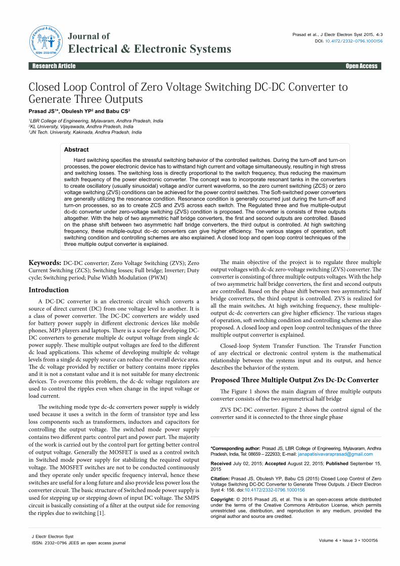
Proposed Three Multiple Output Zvs Dc-Dc ConverterThe Figure 1 shows the main diagram of three multiple outputs
converter consists of the two asymmetrical half bridge
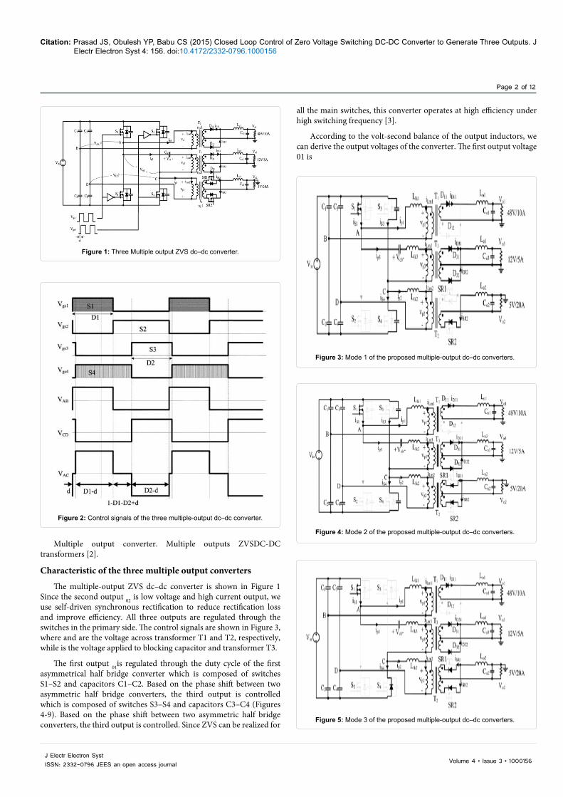
ZVS DC-DC converter. Figure 2 shows the control signal of the converter sand it is connected to the three single phase
AbstractHard switching specifies the stressful switching behavior of the controlled switches. During the turn-off and turn-on
processes, the power electronic device has to withstand high current and voltage simultaneously, resulting in high stress and switching losses. The switching loss is directly proportional to the switch frequency, thus reducing the maximum switch frequency of the power electronic converter. The concept was to incorporate resonant tanks in the converters to create oscillatory (usually sinusoidal) voltage and/or current waveforms, so the zero current switching (ZCS) or zero voltage switching (ZVS) conditions can be achieved for the power control switches. The Soft-switched power converters are generally utilizing the resonance condition. Resonance condition is generally occurred just during the turn-off and turn-on processes, so as to create ZCS and ZVS across each switch. The Regulated three and five multiple-output dc-dc converter under zero-voltage switching (ZVS) condition is proposed. The converter is consists of three outputsaltogether. With the help of two asymmetric half bridge converters, the first and second outputs are controlled. Basedon the phase shift between two asymmetric half bridge converters, the third output is controlled. At high switchingfrequency, these multiple-output dc–dc converters can give higher efficiency. The various stages of operation, softswitching condition and controlling schemes are also explained. A closed loop and open loop control techniques of thethree multiple output converter is explained.
Journal of Electrical & Electronic SystemsJo
urna
l of E
lectrical & ElectronicSystem
s
ISSN: 2332-0796
Citation: Prasad JS, Obulesh YP, Babu CS (2015) Closed Loop Control of Zero Voltage Switching DC-DC Converter to Generate Three Outputs. J Electr Electron Syst 4: 156. doi:10.4172/2332-0796.1000156
Page 2 of 12
Volume 4 • Issue 3 • 1000156J Electr Electron SystISSN: 2332-0796 JEES an open access journal
Multiple output converter. Multiple outputs ZVSDC-DC transformers [2].
Characteristic of the three multiple output converters
The multiple-output ZVS dc–dc converter is shown in Figure 1 Since the second output 02 is low voltage and high current output, we use self-driven synchronous rectification to reduce rectification loss and improve efficiency. All three outputs are regulated through the switches in the primary side. The control signals are shown in Figure 3, where and are the voltage across transformer T1 and T2, respectively, while is the voltage applied to blocking capacitor and transformer T3.
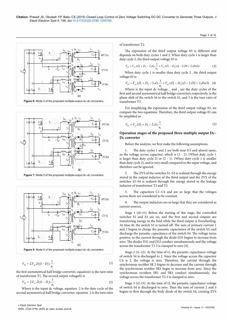
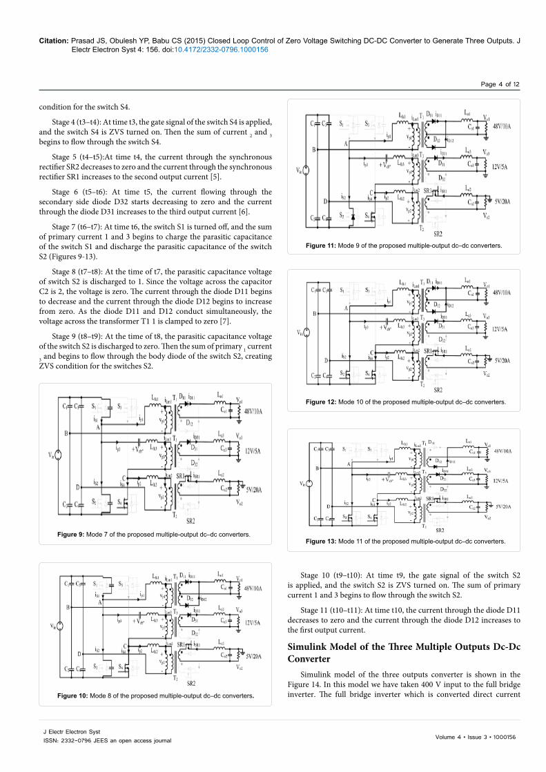
The first output 01is regulated through the duty cycle of the first asymmetrical half bridge converter which is composed of switches S1–S2 and capacitors C1–C2. Based on the phase shift between two asymmetric half bridge converters, the third output is controlled which is composed of switches S3–S4 and capacitors C3–C4 (Figures 4-9). Based on the phase shift between two asymmetric half bridge converters, the third output is controlled. Since ZVS can be realized for
all the main switches, this converter operates at high efficiency under high switching frequency [3].
According to the volt-second balance of the output inductors, we can derive the output voltages of the converter. The first output voltage 01 is
Figure 1: Three Multiple output ZVS dc–dc converter.
Figure 2: Control signals of the three multiple-output dc–dc converter.
Figure 3: Mode 1 of the proposed multiple-output dc–dc converters.
Figure 4: Mode 2 of the proposed multiple-output dc–dc converters.
Figure 5: Mode 3 of the proposed multiple-output dc–dc converters.
Citation: Prasad JS, Obulesh YP, Babu CS (2015) Closed Loop Control of Zero Voltage Switching DC-DC Converter to Generate Three Outputs. J Electr Electron Syst 4: 156. doi:10.4172/2332-0796.1000156
Page 3 of 12
Volume 4 • Issue 3 • 1000156J Electr Electron SystISSN: 2332-0796 JEES an open access journal
01 1 11
12. . (1 ).= −inV V D Dn
(1)
the first asymmetrical half bridge converter, equation1 is the turn ratio of transformer T1. The second output voltage02 is
02 1 11
12. . (1 ).= −inV V D D zdn
(2)
Where is the input dc voltage, equation 2 is the duty cycle of the second asymmetrical half bridge converter, equation 2 is the turn ratio
of transformer T2.
The expression of the third output voltage 03 is different and depends on both duty cycles 1 and 2. When duty cycle 1 is larger than duty cycle 2, the third output voltage 03 is
03 1 2 1 23
1.( 2. ). .( ).(1 2. 1 2. 1 3)= + − + − − +in inV V D D d V D D D d nn
(3)
When duty cycle 1 is smaller than duty cycle 2 , the third output voltage 03 is
03 1 2 1 23
1.( 2. ). .( ).(1 2. 2 2. 1 3)= + − + − − +in inV V D D d V D D D d nn
(4)
Where is the input dc voltage, 1 and 2 are the duty cycles of the first and second asymmetrical half bridge converters respectively, is the phase shift of the switch S4 to the switch S1, and 3 is the turn ratio of transformer T3.
For simplifying the expression of the third output voltage 03, we compare the two equations. Therefore, the third output voltage 03 can be simplified as
03 1 23
1.( 2. ).= + −inV V D D dn
(5)
Operation stages of the proposed three multiple output Dc–Dc converter
Before the analysis, we first make the following assumptions.
1. The duty cycles 1 and 2 are both near 0.5 and almost same, so the voltage across capacitor, which is (1 - 2). (When duty cycle 1 is larger than duty cycle 2) or (2 - 1). (When duty cycle 1 is smaller than duty cycle 2), and is very small compared to the input voltage, and therefore can be ignored.
2. The ZVS of the switches S1–S2 is realized through the energy stored in the output inductor of the third output and the ZVS of the switches S3–S4 is realized through the energy stored in the leakage inductor of transformer T2 and T3.
3. The capacitors C1–C4 and are so large that the voltages across them are considered to be constant.
4. The output inductors are so large that they are considered as current sources.
Stage 1 (t0–t1): Before the starting of this stage, the controlled switches S1 and S3 are on, and the first and second outputs are transferring energy to the load while the third output is freewheeling. At time t0, the switch S3 is turned off. The sum of primary current 1 and 2 begins to charge the parasitic capacitance of the switch S3, and discharge the parasitic capacitance of the switch S4. The voltage turns positive, so the current through the diode D31 begins to increase from zero. The diodes D31 and D32 conduct simultaneously and the voltage across the transformer T3 3 is clamped to zero [4].
Stage 2 (t1–t2): At the time of t1, the parasitic capacitance voltage of switch S4 is discharged to 2. Since the voltage across the capacitor C4 is 2, the voltage is zero. Therefore, the current through the synchronous rectifier SR 2 begins to decrease and the current through the synchronous rectifier SR1 begin to increase from zero. Since the synchronous rectifiers SR1 and SR2 conduct simultaneously, the voltage across the transformer T2 2 is clamped to zero.
Stage 3 (t2–t3): At the time of t2, the parasitic capacitance voltage of switch S4 is discharged to zero. Then the sum of current 2 and 3 begins to flow through the body diode of the switch S4, creating ZVS
Figure 6: Mode 4 of the proposed multiple-output dc–dc converters.
Figure 7: Mode 5 of the proposed multiple-output dc–dc converters.
Figure 8: Mode 6 of the proposed multiple-output dc–dc converters.
Citation: Prasad JS, Obulesh YP, Babu CS (2015) Closed Loop Control of Zero Voltage Switching DC-DC Converter to Generate Three Outputs. J Electr Electron Syst 4: 156. doi:10.4172/2332-0796.1000156
Page 4 of 12
Volume 4 • Issue 3 • 1000156J Electr Electron SystISSN: 2332-0796 JEES an open access journal
condition for the switch S4.
Stage 4 (t3–t4): At time t3, the gate signal of the switch S4 is applied, and the switch S4 is ZVS turned on. Then the sum of current 2 and 3 begins to flow through the switch S4.
Stage 5 (t4–t5):At time t4, the current through the synchronous rectifier SR2 decreases to zero and the current through the synchronous rectifier SR1 increases to the second output current [5].
Stage 6 (t5–t6): At time t5, the current flowing through the secondary side diode D32 starts decreasing to zero and the current through the diode D31 increases to the third output current [6].
Stage 7 (t6–t7): At time t6, the switch S1 is turned off, and the sum of primary current 1 and 3 begins to charge the parasitic capacitance of the switch S1 and discharge the parasitic capacitance of the switch S2 (Figures 9-13).
Stage 8 (t7–t8): At the time of t7, the parasitic capacitance voltage of switch S2 is discharged to 1. Since the voltage across the capacitor C2 is 2, the voltage is zero. The current through the diode D11 begins to decrease and the current through the diode D12 begins to increase from zero. As the diode D11 and D12 conduct simultaneously, the voltage across the transformer T1 1 is clamped to zero [7].
Stage 9 (t8–t9): At the time of t8, the parasitic capacitance voltage of the switch S2 is discharged to zero. Then the sum of primary 1 current 3 and begins to flow through the body diode of the switch S2, creating ZVS condition for the switches S2.
Stage 10 (t9–t10): At time t9, the gate signal of the switch S2 is applied, and the switch S2 is ZVS turned on. The sum of primary current 1 and 3 begins to flow through the switch S2.
Stage 11 (t10–t11): At time t10, the current through the diode D11 decreases to zero and the current through the diode D12 increases to the first output current.
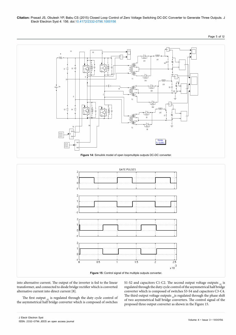
Simulink Model of the Three Multiple Outputs Dc-Dc Converter
Simulink model of the three outputs converter is shown in the Figure 14. In this model we have taken 400 V input to the full bridge inverter. The full bridge inverter which is converted direct current
Figure 9: Mode 7 of the proposed multiple-output dc–dc converters.
Figure 10: Mode 8 of the proposed multiple-output dc–dc converters.
Figure 11: Mode 9 of the proposed multiple-output dc–dc converters.
Figure 12: Mode 10 of the proposed multiple-output dc–dc converters.
Figure 13: Mode 11 of the proposed multiple-output dc–dc converters.
Citation: Prasad JS, Obulesh YP, Babu CS (2015) Closed Loop Control of Zero Voltage Switching DC-DC Converter to Generate Three Outputs. J Electr Electron Syst 4: 156. doi:10.4172/2332-0796.1000156
Page 5 of 12
Volume 4 • Issue 3 • 1000156J Electr Electron SystISSN: 2332-0796 JEES an open access journal
into alternative current. The output of the inverter is fed to the linear transformer, and connected to diode bridge rectifier which is converted alternative current into direct current [8].
The first output 01 is regulated through the duty cycle control of the asymmetrical half bridge converter which is composed of switches
S1-S2 and capacitors C1-C2. The second output voltage outputs 02 is regulated through the duty cycle control of the asymmetrical half bridge converter which is composed of switches S3-S4 and capacitors C3-C4. The third output voltage outputs 03is regulated through the phase shift of two asymmetrical half bridge converters. The control signal of the proposed three output converter as shown in the Figure 15.
V01
V03
AB
CD
P4
P3
cb
P1
P2
Discrete,Ts = 2e-006 s.
v+-
v
+
-
v
+
-
v
+
-
Vin
1
2
3
T3
1
2
3
T2
In1
Out1
Out2
In1
Out1
Out2
R
L03
L02
L01
gm
CE
gm
CE
gm
CE
gm
CE
D32
D31
D2
D12
D11
D1
i+ -
i+ -
i+ -
C8
C7
C6
C4
C3
C2
C1 1
2
3
T1
Figure 14: Simulink model of open loopmultiple outputs DC-DC converter.
Figure 15: Control signal of the multiple outputs converter.
Citation: Prasad JS, Obulesh YP, Babu CS (2015) Closed Loop Control of Zero Voltage Switching DC-DC Converter to Generate Three Outputs. J Electr Electron Syst 4: 156. doi:10.4172/2332-0796.1000156
Page 6 of 12
Volume 4 • Issue 3 • 1000156J Electr Electron SystISSN: 2332-0796 JEES an open access journal
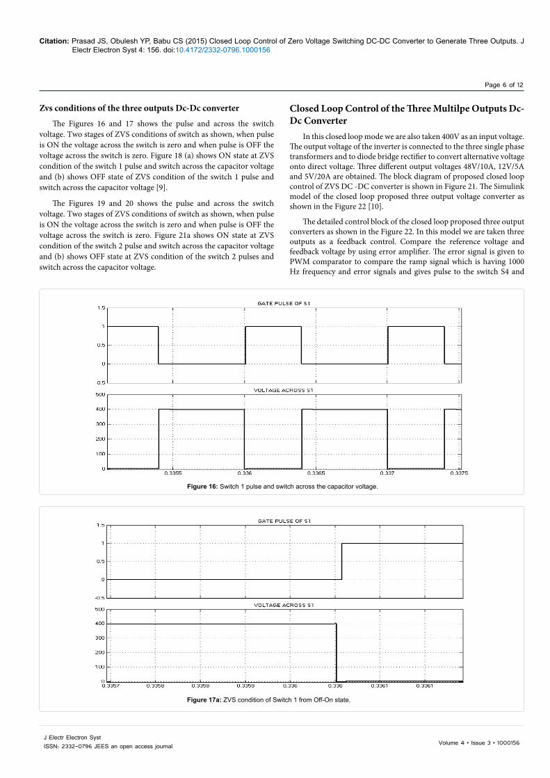
Zvs conditions of the three outputs Dc-Dc converter
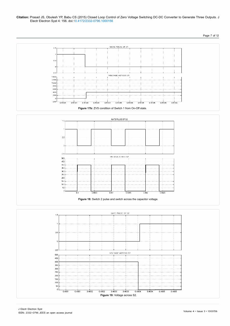
The Figures 16 and 17 shows the pulse and across the switch voltage. Two stages of ZVS conditions of switch as shown, when pulse is ON the voltage across the switch is zero and when pulse is OFF the voltage across the switch is zero. Figure 18 (a) shows ON state at ZVS condition of the switch 1 pulse and switch across the capacitor voltage and (b) shows OFF state of ZVS condition of the switch 1 pulse and switch across the capacitor voltage [9].
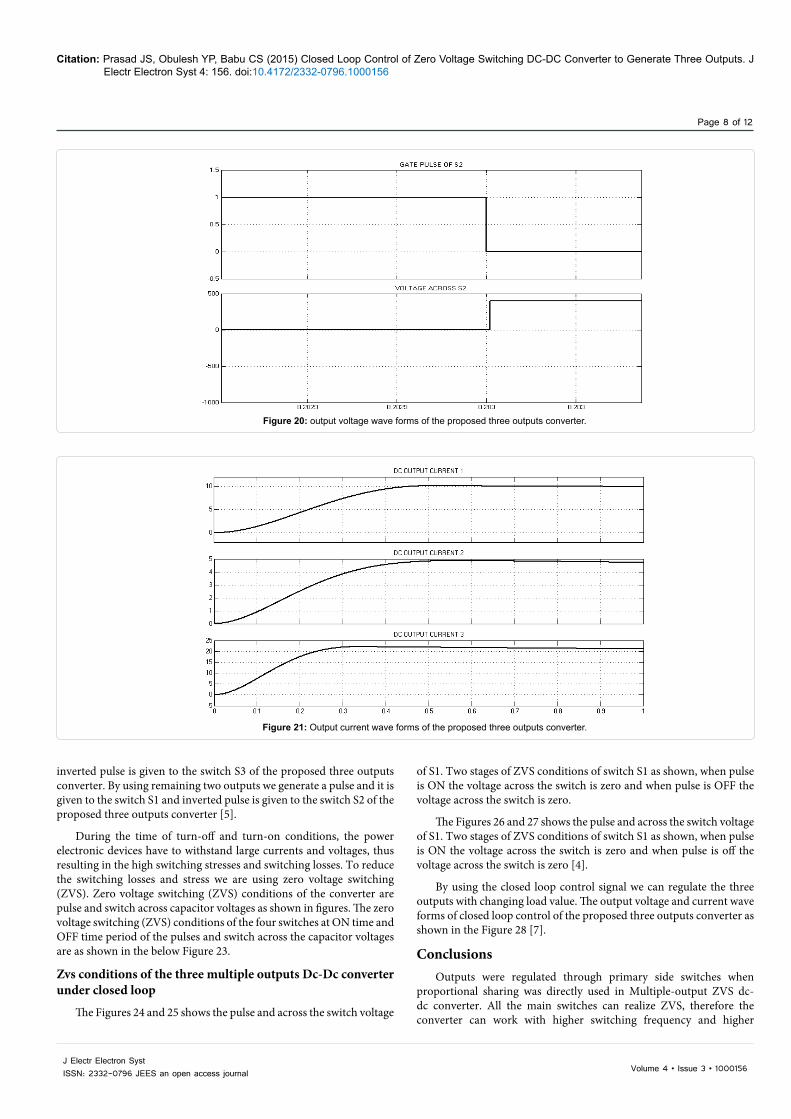
The Figures 19 and 20 shows the pulse and across the switch voltage. Two stages of ZVS conditions of switch as shown, when pulse is ON the voltage across the switch is zero and when pulse is OFF the voltage across the switch is zero. Figure 21a shows ON state at ZVS condition of the switch 2 pulse and switch across the capacitor voltage and (b) shows OFF state at ZVS condition of the switch 2 pulses and switch across the capacitor voltage.
Closed Loop Control of the Three Multilpe Outputs Dc-Dc Converter
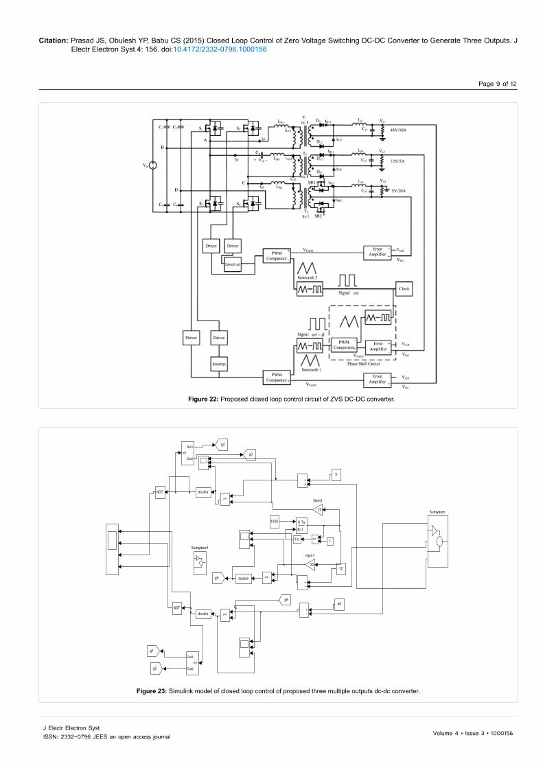
In this closed loop mode we are also taken 400V as an input voltage. The output voltage of the inverter is connected to the three single phase transformers and to diode bridge rectifier to convert alternative voltage onto direct voltage. Three different output voltages 48V/10A, 12V/5A and 5V/20A are obtained. The block diagram of proposed closed loop control of ZVS DC -DC converter is shown in Figure 21. The Simulink model of the closed loop proposed three output voltage converter as shown in the Figure 22 [10].
The detailed control block of the closed loop proposed three output converters as shown in the Figure 22. In this model we are taken three outputs as a feedback control. Compare the reference voltage and feedback voltage by using error amplifier. The error signal is given to PWM comparator to compare the ramp signal which is having 1000 Hz frequency and error signals and gives pulse to the switch S4 and
Figure 16: Switch 1 pulse and switch across the capacitor voltage.
Figure 17a: ZVS condition of Switch 1 from Off-On state.
Citation: Prasad JS, Obulesh YP, Babu CS (2015) Closed Loop Control of Zero Voltage Switching DC-DC Converter to Generate Three Outputs. J Electr Electron Syst 4: 156. doi:10.4172/2332-0796.1000156
Page 7 of 12
Volume 4 • Issue 3 • 1000156J Electr Electron SystISSN: 2332-0796 JEES an open access journal
Figure 17b: ZVS condition of Switch 1 from On-Off state.
Figure 18: Switch 2 pulse and switch across the capacitor voltage.
Figure 19: Voltage across S2.
Citation: Prasad JS, Obulesh YP, Babu CS (2015) Closed Loop Control of Zero Voltage Switching DC-DC Converter to Generate Three Outputs. J Electr Electron Syst 4: 156. doi:10.4172/2332-0796.1000156
Page 8 of 12
Volume 4 • Issue 3 • 1000156J Electr Electron SystISSN: 2332-0796 JEES an open access journal
Figure 20: output voltage wave forms of the proposed three outputs converter.
Figure 21: Output current wave forms of the proposed three outputs converter.
inverted pulse is given to the switch S3 of the proposed three outputs converter. By using remaining two outputs we generate a pulse and it is given to the switch S1 and inverted pulse is given to the switch S2 of the proposed three outputs converter [5].
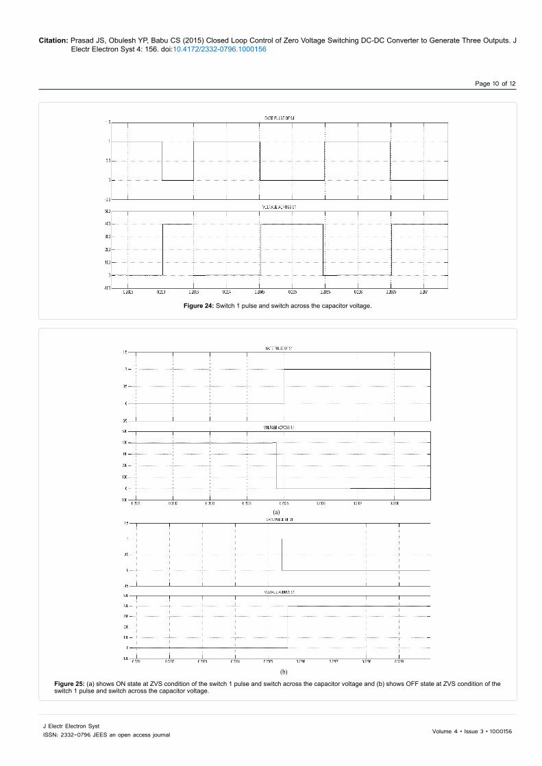
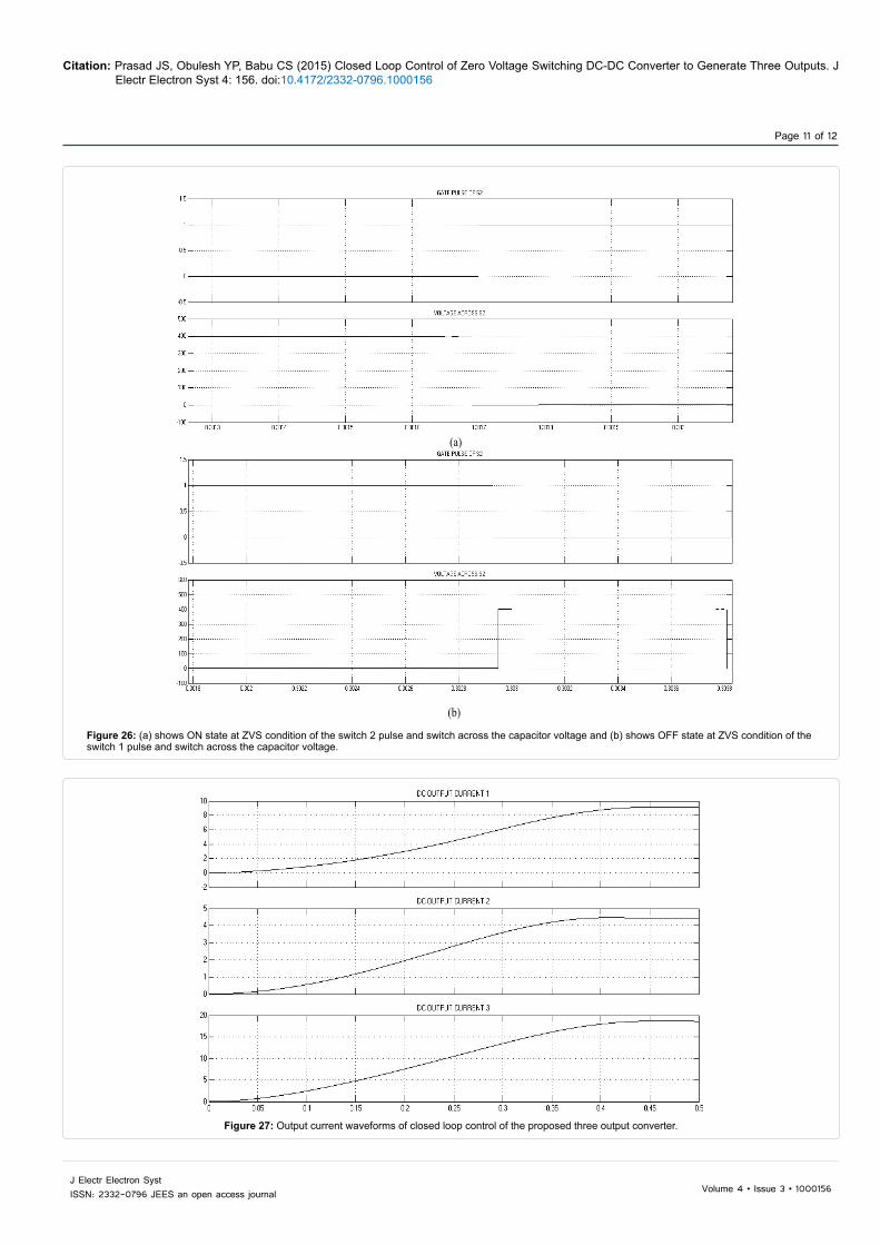
During the time of turn-off and turn-on conditions, the power electronic devices have to withstand large currents and voltages, thus resulting in the high switching stresses and switching losses. To reduce the switching losses and stress we are using zero voltage switching (ZVS). Zero voltage switching (ZVS) conditions of the converter are pulse and switch across capacitor voltages as shown in figures. The zero voltage switching (ZVS) conditions of the four switches at ON time and OFF time period of the pulses and switch across the capacitor voltages are as shown in the below Figure 23.
Zvs conditions of the three multiple outputs Dc-Dc converter under closed loop
The Figures 24 and 25 shows the pulse and across the switch voltage
of S1. Two stages of ZVS conditions of switch S1 as shown, when pulse is ON the voltage across the switch is zero and when pulse is OFF the voltage across the switch is zero.
The Figures 26 and 27 shows the pulse and across the switch voltage of S1. Two stages of ZVS conditions of switch S1 as shown, when pulse is ON the voltage across the switch is zero and when pulse is off the voltage across the switch is zero [4].
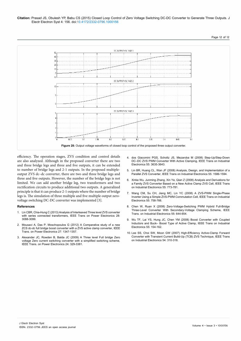
By using the closed loop control signal we can regulate the three outputs with changing load value. The output voltage and current wave forms of closed loop control of the proposed three outputs converter as shown in the Figure 28 [7].
ConclusionsOutputs were regulated through primary side switches when
proportional sharing was directly used in Multiple-output ZVS dc-dc converter. All the main switches can realize ZVS, therefore the converter can work with higher switching frequency and higher
Citation: Prasad JS, Obulesh YP, Babu CS (2015) Closed Loop Control of Zero Voltage Switching DC-DC Converter to Generate Three Outputs. J Electr Electron Syst 4: 156. doi:10.4172/2332-0796.1000156
Page 9 of 12
Volume 4 • Issue 3 • 1000156J Electr Electron SystISSN: 2332-0796 JEES an open access journal
Figure 22: Proposed closed loop control circuit of ZVS DC-DC converter.
1000
1/z
In1
Out1
Out2
In1
Out1
Out2
Subsystem1
Subsystem
>=
>=
>=
>=
NOT
NOT
g5
g4
g3
g2
g1
20
Gain2
20
Gain1
g6
K Ts
z-1
double
double
double
48
1
12
5
Figure 23: Simulink model of closed loop control of proposed three multiple outputs dc-dc converter.
Citation: Prasad JS, Obulesh YP, Babu CS (2015) Closed Loop Control of Zero Voltage Switching DC-DC Converter to Generate Three Outputs. J Electr Electron Syst 4: 156. doi:10.4172/2332-0796.1000156
Page 10 of 12
Volume 4 • Issue 3 • 1000156J Electr Electron SystISSN: 2332-0796 JEES an open access journal
Figure 24: Switch 1 pulse and switch across the capacitor voltage.
(a)
(b)
Figure 25: (a) shows ON state at ZVS condition of the switch 1 pulse and switch across the capacitor voltage and (b) shows OFF state at ZVS condition of the switch 1 pulse and switch across the capacitor voltage.
Citation: Prasad JS, Obulesh YP, Babu CS (2015) Closed Loop Control of Zero Voltage Switching DC-DC Converter to Generate Three Outputs. J Electr Electron Syst 4: 156. doi:10.4172/2332-0796.1000156
Page 11 of 12
Volume 4 • Issue 3 • 1000156J Electr Electron SystISSN: 2332-0796 JEES an open access journal
(a)
(b)
Figure 26: (a) shows ON state at ZVS condition of the switch 2 pulse and switch across the capacitor voltage and (b) shows OFF state at ZVS condition of the switch 1 pulse and switch across the capacitor voltage.
Figure 27: Output current waveforms of closed loop control of the proposed three output converter.
Citation: Prasad JS, Obulesh YP, Babu CS (2015) Closed Loop Control of Zero Voltage Switching DC-DC Converter to Generate Three Outputs. J Electr Electron Syst 4: 156. doi:10.4172/2332-0796.1000156
Page 12 of 12
Volume 4 • Issue 3 • 1000156J Electr Electron SystISSN: 2332-0796 JEES an open access journal
Figure 28: Output voltage waveforms of closed loop control of the proposed three output converter.
efficiency. The operation stages, ZVS condition and control details are also analyzed. Although in the proposed converter there are two and three bridge legs and three and five outputs, it can be extended to number of bridge legs and 2-1 outputs. In the proposed multiple-output ZVS dc–dc converter, there are two and three bridge legs and three and five outputs. However, the number of the bridge legs is not limited. We can add another bridge leg, two transformers and two rectification circuits to produce additional two outputs. A generalized principle is that it can produce 2-1 outputs where the number of bridge legs is. The simulation of three multiple and five multiple output zero-voltage switching DC-DC converter was implemented [3].
References
1. Lin CBR, Chia-Hung C (2013) Analysis of Interleaved Three level ZVS converter with series connected transformers, IEEE Trans on Power Electronics 28:3088-3099.
2. Mousavi A, Das P, Moschopoulos G (2012) A Comparative study of a newZCS dc-dc full bridge boost converter with a ZVS active clamp converter, IEEE Trans. on Power Electronics 27: 1347-1357.
3. Alexander JC, Rowden B, Balda JC (2009) A Three level Full bridge Zerovoltage Zero current switching converter with a simplified switching scheme, IEEE Trans. on Power Electronics 24: 329-3381.
4. dos Giacomini PGS, Scholtz JS, Mezaroba M (2008) Step-Up/Step-DownDC–DC ZVS PWM Converter With Active Clamping, IEEE Trans on IndustrialElectronics 55: 3635-3643.
5. Lin BR, Huang CL, Wan JF (2008) Analysis, Design, and Implementation of aParallel ZVS Converter, IEEE Trans on Industrial Electronics 55: 1586-1594.
6. Xinke Wu, Junming Zhang, Xin Ye, Qian Z (2008) Analysis and Derivations for a Family ZVS Converter Based on a New Active Clamp ZVS Cell, IEEE Transon Industrial Electronics 55: 773-781.
7. Wang CM, Su CH, Jiang MC, Lin YC (2008) A ZVS-PWM Single-PhaseInverter Using a Simple ZVS-PWM Commutation Cell, IEEE Trans on Industrial Electronics 55: 758-766.
8. Chen W, Ruan X (2008) Zero-Voltage-Switching PWM Hybrid Full-BridgeThree-Level Converter With Secondary-Voltage Clamping Scheme, IEEETrans. on Industrial Electronics 55: 644-654.
9. Wu TF, Lai YS, Hung JC, Chen YM (2008) Boost Converter with CoupledInductors and Buck– Boost Type of Active Clamp, IEEE Trans on IndustrialElectronics 55: 154-162.
10. Lee SS, Choi SW, Moon GW (2007) High-Efficiency Active-Clamp Forward Converter with Transient Current Build-Up (TCB) ZVS Technique, IEEE Transon Industrial Electronics 54: 310-318.