Embed Size (px)
Citation preview
CARTESIAN FEEDBACK CONTROL
FOR MRI TRANSMITTER ARRAY SYSTEMS
A DISSERTATION
SUBMITTED TO THE DEPARTMENT OF ELECTRICAL
ENGINEERING
AND THE COMMITTEE ON GRADUATE STUDIES
OF STANFORD UNIVERSITY
IN PARTIAL FULFILLMENT OF THE REQUIREMENTS
FOR THE DEGREE OF
DOCTOR OF PHILOSOPHY
Marta Gaia Zanchi
May 2010

http://creativecommons.org/licenses/by-nc/3.0/us/
This dissertation is online at: http://purl.stanford.edu/jd326wm8459
© 2010 by Marta Gaia Zanchi. All Rights Reserved.
Re-distributed by Stanford University under license with the author.
This work is licensed under a Creative Commons Attribution-Noncommercial 3.0 United States License.
ii

I certify that I have read this dissertation and that, in my opinion, it is fully adequatein scope and quality as a dissertation for the degree of Doctor of Philosophy.
John Pauly, Primary Adviser
I certify that I have read this dissertation and that, in my opinion, it is fully adequatein scope and quality as a dissertation for the degree of Doctor of Philosophy.
Thomas Lee
I certify that I have read this dissertation and that, in my opinion, it is fully adequatein scope and quality as a dissertation for the degree of Doctor of Philosophy.
Greig Cameron Scott
Approved for the Stanford University Committee on Graduate Studies.
Patricia J. Gumport, Vice Provost Graduate Education
This signature page was generated electronically upon submission of this dissertation in electronic format. An original signed hard copy of the signature page is on file inUniversity Archives.
iii
Preface
Accurate control of the radio-frequency (RF) electromagnetic fields in Magnetic Res-
onance Imaging (MRI) is necessary to ensure patient safety and provide high-quality
diagnostic capabilities. Precise control is however becoming increasingly difficult to
achieve, given the recent trends toward high fields and transmitter array systems. At
high fields, imaging is performed in a frequency regime where the wavelength is on the
order of, or smaller than, the dimensions of the human body. This leads to prominent
wave behavior, non-uniform field patterns, and increased power deposition. Multi-
element transmitter array systems with independent phase and amplitude control of
their elements support methods that can mitigate these problems. However, in turn,
they demand high fidelity RF reproduction and may lead to undesired electromagnetic
interactions between elements of the arrays and with interventional devices.
Frequency-offset Cartesian feedback can be used to address all of these issues. In
combination with the use of polyphase error amplifiers—to implement a low-IF control
bandwidth—Cartesian feedback can be used with MRI power amplifiers and transmit
coils to increase the fidelity of RF reproduction, without the in-bandwidth DC-offsets
and quadrature mismatches that may lead to imaging artifacts such as bright spots
and ghosting. In addition, the control system—which includes autotuning circuitry
for stability and vector multipliers circuitry for feedback manipulation—can be used
to tune the series output impedance of these amplifiers, thereby reducing the like-
lihood of interactions between elements of transmit array systems. Furthermore, a
miniaturized variation of the control system (called Active Cable Trap) can be used
on guidewires to suppress undesired currents elicited by coupling with the RF fields
of the transmit coils.
iv

In an era of rapid progress in high field MRI for clinical applications, the frequency-
offset Cartesian feedback method and system thus promises to address many of the
challenges faced by designers of multi-element transmitter array systems.
v

Acknowledgements
Had I not been fortunate enough to meet and work with Dr. Greig Scott during the
past four years, this dissertation would look very different. It would use an excessive
number of words (Dr. Scott would tactfully describe it as “verbose”) to explain far
fewer interesting concepts and results. He is one of the most intellectually honest,
creative, and enthusiastic scientists I have ever met.
I am equally fortunate to have been guided along the Ph.D. path by Prof. John
Pauly. He has always been encouraging, sympathetic, and available whenever I was
in need of help or advice. I am particularly grateful that he has always stood by
me when I was planning one of my new summer adventures, whether I wanted to
join a start-up company in Fremont, California, or work in the government offices in
Rockville, Maryland. These great opportunities would not have come true without
his ongoing support.
Prof. Thomas Lee is one of the most unexpected surprises that Stanford has
thrown at me. The little time I was privileged to spend in conversations with him has
made my Ph.D. journey much more enjoyable and has given me strength and hope
for what would come after. Of the 2,000 people who populate the world, he shines as
one of my favorites. Thinking of him, I am reminded of Friedrich Nietzsche’s famous
quote, ”One must have chaos [in his office] to give birth to a dancing star.” Indeed!
To Prof. Michael McConnell, I want to express my deepest appreciation for join-
ing Dr. Scott, Prof. Pauly, and Prof. Lee in my oral dissertation committee. I am
particularly happy to have had Prof. Jelena Vuckovic chair the committee. Prof.
Vuckovic taught the very first class—Applied Quantum Mechanics— I took at Stan-
ford in the fall of 2006. With her strength, independence, and hard work, she has
vi

always been a role model for me.
Evelin Sullivan has been my great friend and writing tutor at the Stanford School
of Engineering since 2007. In the past three years, she read almost every single page
I have written (God knows I wrote many!), and patiently educated me in the art of
clear and logical writing... even when this meant correcting my mistakes seven times
in a row. With her, I share the passion for a well written document and the joy of
scooter riding, to which I am proud and happy to have introduced her.
I am indebted to many people at the Magnetic Resonance Systems Research Labo-
ratory (MRSRL). All of them have been great friends, helpful colleagues, and patient
teachers. Prof. Albert Macovski is, to say the least, an inspiration to build great
things that last generations and beyond. Prof. Dwight Nishimura, Dr. Adam Kerr,
Prof. Steven Conolly, and Dr. William Overall have been always supportive, en-
couraging, and generous with their time and consideration. Joelle Barral and Pascal
Stang are destined to amazing careers and I am privileged to have received their help
and enjoyed their friendship. I am grateful and happy to have been at MRSRL with
Hattie Dong, Thomas Grafendorfer, Okai Addy, Joseph Cheng, Emine Saritas, Kim
Shultz, and many others. I thank Ross Venook for the research he has done before
me, for the interest he has demonstrated in what I built on his legacy, and for always
greeting me with a smile and a word of encouragement. I am grateful to Lily Shuye
Huan for her work and assistance throughout the years. My deepest thanks go to
Maryam Etezadi-Amoli, the kindest, sweetest, most selfless, as well as one of the most
intelligent young women I have ever met. I am proud she gave me her friendship and
I hope it will continue for many, many years ahead.
A few more remarkable men at and around Stanford have made a strong impression
in my life. I want to thank in particular Prof. Robert Dawson at the Department of
Art and Art History in Stanford University. In 2006, he opened the doors of his office
(and his analog photography darkroom) to me, and later helped me being admitted
to the M.F.A. program in Photography at the Academy of Art University in San
Francisco. Here, I want to thank Prof. Will Mosgrove for seeing me as an artist with
an engineering degree, rather than as an engineer with a digital camera.
The summer of 2007 in Volterra Semiconductors, Fremont, California, was beyond
vii

my expectations and the opportunity to meet a number of wonderful people including
Som Chakraborty, Milovan Glogovac, Alex Ikriannikov, Michael McJimsey, and many
others. I am very grateful to Ognjen Djekic for welcoming me in his System Design
group and for being a great boss then, and a great friend after.
I want to acknowledge the support and great work of the organizers and teachers
at the Summer Institute for Entrepreneurship at the Stanford Graduate School of
Business, with whom I was privileged to spend the summer of 2008.
Dr. Sunder Rajan mentored me during the summer of 2009 at the Office of Device
Evaluation, Food & Drug Administration, in Rockville, Maryland. I am very grateful
for he was the kindest and most understanding mentor I could have ever hoped for.
I am fortunate to have worked with him and to have had the opportunity to know
him and his lovely wife outside of work. He is an example of generosity and, with his
work for Habitat for Humanity, he inspired me to dedicate more time volunteering
for the Peninsula Humane Society.
In and outside Stanford, I was blessed with the friendship of some truly special
people. I want to thank Wei Wu and Forrest Foust for the great time spent together
in conversations about comics, art, Chinese anecdotes, dreams, Wisconsin cheese,
traveling, and so much more. I thank Maryam Fathi for the great work we did (and
all the fun we had while doing it) in the radiofrequency classes we took together as
a team during the past four years. Of Alex Tung, I cherish the memories of the
time spent together in the basement of Packard. He is not with us anymore, but his
spirit is, and so are the beautiful fruits of his humanitarian work. From all over the
world, my dear friends Alessandro Rossi, Lara Gherardi, Alessandro Restelli, Alberto
Carrera, and Ivan Labanca have always encouraged me to be strong and helped me
to find happiness in life. I hope they know just how much I treasure their beautiful
friendship.
To my parents, Paolo Zanchi and Claudia Modesti, I owe a tremendous amount of
gratitude. They have always loved and supported me unconditionally, even when my
pursuit of happiness meant taking away a piece of theirs. There is not a single day in
which I do not feel fortunate and proud to say that I am their daughter and biggest
fan. I am grateful to my grandma Natalina Nervi, to my cousins, nephews, aunties
viii

and uncles, and to all the rest of my family for their encouragement and affection. I
miss them all, dearly. I thank my new extended Garcea family as well, in particular
Bruno, Maura, Rosetta, Teresa, Dino, and their kind sisters, for welcoming me in
their homes as if I had always been a part of them.
Finally, I thank my husband, Giovanni Garcea. He is my best friend, my playmate,
my anchor to sanity, my dream maker. With his caring presence, he always reminds
me of the truly important things in life. With his example, he teaches me that there
are no boundaries to what we can pursue. With his passion, he makes every day
worth living to the fullest. This thesis is dedicated to him, with love.
E quidi uscimmo a riveder le stelle.
ix

Contents
Preface iv
Acknowledgements vi
1 Introduction 1
1.1 MR Imaging . . . . . . . . . . . . . . . . . . . . . . . . . . . . . . . . 2
1.2 MR Trends and Challenges . . . . . . . . . . . . . . . . . . . . . . . . 6
1.2.1 Towards higher RF bandwidth and frequency . . . . . . . . . 6
1.2.2 Towards Arrays of Transmitters . . . . . . . . . . . . . . . . . 7
1.2.3 Towards Interventional MRI . . . . . . . . . . . . . . . . . . . 8
1.3 Translating Challenges into Goals . . . . . . . . . . . . . . . . . . . . 10
1.4 Dissertation Overview . . . . . . . . . . . . . . . . . . . . . . . . . . 11
2 Cartesian Feedback 13
2.1 Introduction . . . . . . . . . . . . . . . . . . . . . . . . . . . . . . . . 13
2.2 Cartesian Feedback . . . . . . . . . . . . . . . . . . . . . . . . . . . . 13
2.2.1 Brief History . . . . . . . . . . . . . . . . . . . . . . . . . . . 13
2.2.2 Classic Cartesian Feedback . . . . . . . . . . . . . . . . . . . . 15
2.2.3 Problems of Classic Cartesian Feedback . . . . . . . . . . . . . 19
2.2.4 Towards a Modified Cartesian Feedback Architecture . . . . . 21
2.2.5 Adapting Cartesian Feedback to Application in MRI . . . . . 23
2.3 Alternatives to Cartesian Feedback . . . . . . . . . . . . . . . . . . . 24
2.4 Summary . . . . . . . . . . . . . . . . . . . . . . . . . . . . . . . . . 28
x
3 Active Polyphase Amplifiers 29
3.1 Introduction . . . . . . . . . . . . . . . . . . . . . . . . . . . . . . . . 29
3.2 Brief History . . . . . . . . . . . . . . . . . . . . . . . . . . . . . . . 29
3.3 Requirements . . . . . . . . . . . . . . . . . . . . . . . . . . . . . . . 30
3.4 Theory . . . . . . . . . . . . . . . . . . . . . . . . . . . . . . . . . . . 33
3.5 Experiments . . . . . . . . . . . . . . . . . . . . . . . . . . . . . . . . 40
3.5.1 Results . . . . . . . . . . . . . . . . . . . . . . . . . . . . . . . 41
3.6 Summary . . . . . . . . . . . . . . . . . . . . . . . . . . . . . . . . . 45
4 System Design 46
4.1 Introduction . . . . . . . . . . . . . . . . . . . . . . . . . . . . . . . . 46
4.2 Motivations, Requirements and Objectives . . . . . . . . . . . . . . . 46
4.3 High-Level System Preview . . . . . . . . . . . . . . . . . . . . . . . 49
4.4 The Transmitter: Genie . . . . . . . . . . . . . . . . . . . . . . . . . 51
4.4.1 Image Reject Down-Converter . . . . . . . . . . . . . . . . . . 53
4.4.2 DC Management Circuitry . . . . . . . . . . . . . . . . . . . . 56
4.4.3 Polyphase Amplifier Loop Filter . . . . . . . . . . . . . . . . . 57
4.4.4 Mixers and Phase Shift Control . . . . . . . . . . . . . . . . . 57
4.4.5 Additional Genie Components . . . . . . . . . . . . . . . . . . 59
4.5 Closing the Loop . . . . . . . . . . . . . . . . . . . . . . . . . . . . . 60
4.5.1 Power Amplifiers . . . . . . . . . . . . . . . . . . . . . . . . . 61
4.5.2 Loads . . . . . . . . . . . . . . . . . . . . . . . . . . . . . . . 62
4.5.3 Coupling devices . . . . . . . . . . . . . . . . . . . . . . . . . 63
4.5.4 Auto-Calibration Network . . . . . . . . . . . . . . . . . . . . 65
4.5.5 Medusa . . . . . . . . . . . . . . . . . . . . . . . . . . . . . . 68
4.5.6 PE001 Card and GUI Interface . . . . . . . . . . . . . . . . . 69
4.5.7 AVRmini and Matlab Interface . . . . . . . . . . . . . . . . . 69
4.6 Analysis of Performance . . . . . . . . . . . . . . . . . . . . . . . . . 70
4.7 Analysis of Stability . . . . . . . . . . . . . . . . . . . . . . . . . . . 72
4.8 Summary . . . . . . . . . . . . . . . . . . . . . . . . . . . . . . . . . 74
xi
5 Improving the Fidelity of RF Reproduction 75
5.1 Introduction . . . . . . . . . . . . . . . . . . . . . . . . . . . . . . . . 75
5.2 Nature of Amplifier Distortion . . . . . . . . . . . . . . . . . . . . . . 76
5.3 Reduced AM-AM, AM-PM Distortion . . . . . . . . . . . . . . . . . 78
5.3.1 Voltage-Mode Amplitude Test . . . . . . . . . . . . . . . . . . 79
5.3.2 Current-Mode Amplitude Test . . . . . . . . . . . . . . . . . . 80
5.4 Reduced Two-Tone and QAM Distortion . . . . . . . . . . . . . . . . 82
5.4.1 Two-Tone Test . . . . . . . . . . . . . . . . . . . . . . . . . . 82
5.4.2 QAM Constellation Test . . . . . . . . . . . . . . . . . . . . . 84
5.5 Reduced MRI Pulse Distortion . . . . . . . . . . . . . . . . . . . . . . 86
5.5.1 Sinc Pulse Linearization Test . . . . . . . . . . . . . . . . . . 87
5.5.2 VSS Pulse Linearization Test . . . . . . . . . . . . . . . . . . 89
5.6 Effect of Linearization on Magnetization . . . . . . . . . . . . . . . . 90
5.7 Closed Loop Image Rejection Performance . . . . . . . . . . . . . . . 93
5.8 Summary . . . . . . . . . . . . . . . . . . . . . . . . . . . . . . . . . 93
6 Manipulating the Amplifier Impedance 95
6.1 Introduction . . . . . . . . . . . . . . . . . . . . . . . . . . . . . . . . 95
6.2 The problem of Coil Interactions . . . . . . . . . . . . . . . . . . . . 96
6.2.1 Available Methods . . . . . . . . . . . . . . . . . . . . . . . . 97
6.3 Theory of Impedance Manipulation . . . . . . . . . . . . . . . . . . . 101
6.4 Load Pull Setup . . . . . . . . . . . . . . . . . . . . . . . . . . . . . . 103
6.5 Impedance Control System Configuration . . . . . . . . . . . . . . . . 105
6.6 Experiments . . . . . . . . . . . . . . . . . . . . . . . . . . . . . . . . 109
6.6.1 With Single Power Amplifier . . . . . . . . . . . . . . . . . . . 109
6.6.2 With Balanced Power Amplifier . . . . . . . . . . . . . . . . . 110
6.7 Summary . . . . . . . . . . . . . . . . . . . . . . . . . . . . . . . . . 112
7 Conclusion 114
A Active Cable Trap 117
A.1 Introduction . . . . . . . . . . . . . . . . . . . . . . . . . . . . . . . . 117
xii

A.2 Theory and Previous Work . . . . . . . . . . . . . . . . . . . . . . . . 118
A.3 Feedback Method for Current Attenuation . . . . . . . . . . . . . . . 119
A.3.1 Toroidal Sensor . . . . . . . . . . . . . . . . . . . . . . . . . . 121
A.3.2 Quadrature Demodulator . . . . . . . . . . . . . . . . . . . . . 122
A.3.3 Polyphase Loop Error Amplifiers . . . . . . . . . . . . . . . . 123
A.3.4 Quadrature Modulator . . . . . . . . . . . . . . . . . . . . . . 124
A.3.5 Toroidal actuator . . . . . . . . . . . . . . . . . . . . . . . . . 124
A.4 Validation . . . . . . . . . . . . . . . . . . . . . . . . . . . . . . . . . 125
Bibliography 128
xiii

List of Tables
3.1 Simulated and Measured Sideband Rejection at Different Center Fre-
quencies of the Polyphase Passband . . . . . . . . . . . . . . . . . . . 45
4.1 S-parameters of custom-made coupler. Port 1 = Input; Port 2 = Out-
put; Port 3 = Voltage Sample; Port 4 = Current Sample. . . . . . . . 65
4.2 S-parameters of C7149 coupler by Werlatone. Port 1 = Input; Port 2 =
Output; Port 3 = Forward Voltage Sample; Port 4 = Reverse Voltage
Sample. . . . . . . . . . . . . . . . . . . . . . . . . . . . . . . . . . . 65
4.3 Gain and maximum input and output levels of the main loop com-
ponents. The maximum up-mixer output is taken after the on-board
filters. The maximum down-mixer input is valid at minimum gain set-
ting; typically, the gain is 0±3 dB and the corresponding maximum
input is +2∓3 dBm. The power amplifier is the custom-made ampli-
fier built using an AN779H 20 W predriver and an AR313 amplifier by
Communication Concepts, Inc. . . . . . . . . . . . . . . . . . . . . . . 74
5.1 Measured Sideband Rejection of the Closed Loop FOCF System . . . 94
xiv

List of Figures
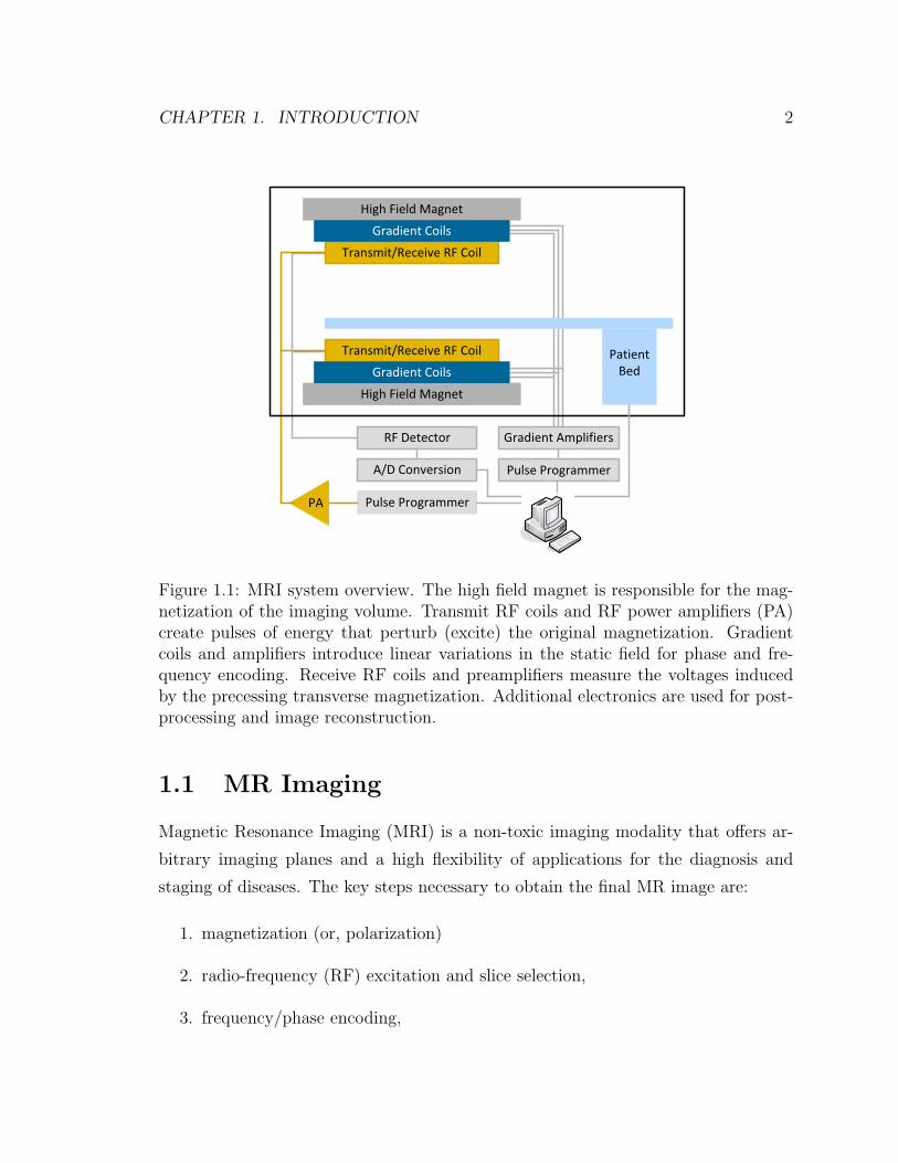
1.1 MRI system overview. The high field magnet is responsible for the
magnetization of the imaging volume. Transmit RF coils and RF
power amplifiers (PA) create pulses of energy that perturb (excite) the
original magnetization. Gradient coils and amplifiers introduce linear
variations in the static field for phase and frequency encoding. Receive
RF coils and preamplifiers measure the voltages induced by the pre-
cessing transverse magnetization. Additional electronics are used for
post-processing and image reconstruction. . . . . . . . . . . . . . . . 2
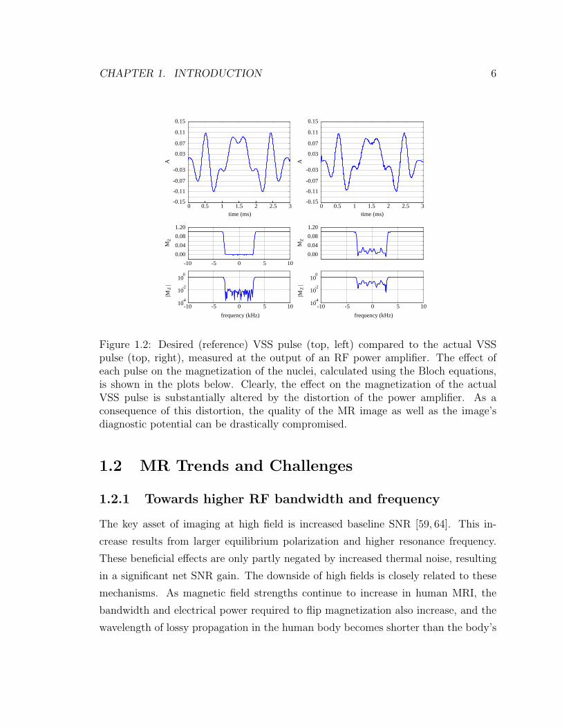
1.2 Desired (reference) VSS pulse (top, left) compared to the actual VSS
pulse (top, right), measured at the output of an RF power amplifier.
The effect of each pulse on the magnetization of the nuclei, calculated
using the Bloch equations, is shown in the plots below. Clearly, the
effect on the magnetization of the actual VSS pulse is substantially
altered by the distortion of the power amplifier. As a consequence of
this distortion, the quality of the MR image as well as the image’s
diagnostic potential can be drastically compromised. . . . . . . . . . 6
xv

1.3 Measurement setup (top) and measured currents and heating (bot-
tom) induced by the MRI RF field in a guidewire. The measurement
setup shows a previously developed optically-coupled current moni-
toring device, which consists of toroidal sensor, transmitter, receiver,
and display of the measured signals (in this case, an oscilloscope). The
guidewire was fed in the cavity of the toroidal sensor. The temperature
rise at the guidewire tip was measured with a commercial temperature
sensor. At increasing body coil excitation, the measured current (bot-
tom, right) increases linearly and the measured temperature increase
(bottom, left) increases quadratically. . . . . . . . . . . . . . . . . . . 9
2.1 Simplified schematic of a Cartesian feedback control system for power
amplifier linearization. The basic Cartesian loop consists of two identi-
cal feedback circuits operating independently on the quadrature (I/Q)
channels. Each of the quadrature baseband inputs is applied to a dif-
ferential amplifier, with the resulting difference (error) signals being
modulated (up-converted) onto quadrature carriers at the local oscil-
lator frequency and then combined to drive the power amplifier. A
sampled version of the power amplifier output is quadrature-down-
converted (synchronously with the up-conversion process). The result-
ing quadrature feedback signals form the second inputs to the differ-
ential integrators, completing the two feedback loops. . . . . . . . . . 15
2.2 Classic loop amplifiers. In a Cartesian feedback system, these ampli-
fiers subtract the reference and feedback signal, amplify the resulting
difference, and are responsible for the loop compensation. . . . . . . . 16
2.3 Classic loop amplifiers response. Reference signal, feedback signal, and
error amplification are at DC. . . . . . . . . . . . . . . . . . . . . . . 17
2.4 Complex bandpass amplifiers response. A reference signal, feedback
signal, and error amplification shifted at a complex IF frequency moves
the control bandwidth away from the frequencies where DC offset and
quadrature mismatches exist. . . . . . . . . . . . . . . . . . . . . . . 22
xvi

3.1 Control bandwidth options. In a classic pair of lowpass amplifiers,
amplification and subtraction between the reference input signals and
feedback signals occur at DC (top). A pair of bandpass amplifier cre-
ates two separate bandwidths at both positive and negative frequencies
(middle). Polyphase amplifiers, instead, create a single complex band-
pass control bandwidth (bottom); hence, they selectively amplify the
desired signals over quadrature mismatches and DC offsets. . . . . . . 31
3.2 Simplified schematic (left) and frequency response (right) of the fully-
differential polyphase difference amplifiers that have been used as the
loop error amplifiers of the frequency-offset Cartesian feedback system
described in this dissertation. . . . . . . . . . . . . . . . . . . . . . . 33
3.3 Actual polyphase amplifier transfer function with varying operational
amplifier gain (left, pole frequency is constant) and pole frequency
(right, gain is constant). If the gain-bandwidth product of the opera-
tional amplifier is the same, the effects of these non-idealities on the
desired polyphase transfer function are virtually indistinguishable. . . 38
3.4 Picture and simplified schematic of PCB for testing of polyphase am-
plifiers. The polyphase amplifiers can be tested with either two fully-
differential input signals or two positive input signals (the negative
inputs being AC-grounded). . . . . . . . . . . . . . . . . . . . . . . . 40
3.5 Normalized real input (i, q) to real output (I, Q) simulated trans-
fer functions. The latter can be also measured by driving the PCB
polyphase amplifiers with only one non-zero quadrature input signal (i
or q) at a time. . . . . . . . . . . . . . . . . . . . . . . . . . . . . . . 41
3.6 Up, Um, Vp, Vm simulated transfer functions obtained by combining the
functions in Figure 3.5. . . . . . . . . . . . . . . . . . . . . . . . . . . 42
3.7 Overall simulated transfer functions of the polyphase amplifiers ob-
tained by combining the functions in Figure 3.6. The desired frequency
response is obtained by merging Up with the mirrored Vm. The mirror
frequency response is obtained by merging Vp with the mirrored Um. . 43
xvii

3.8 Experimental transfer functions of the polyphase amplifiers. These
functions were constructed from the normalized real input (i, q) to
real output (I, Q) transfer functions measured by driving the amplifiers
with only one non-zero quadrature input signal (i or q) at a time. . . 44
4.1 Simplified hardware diagram of the frequency-offset Cartesian feedback
system. In addition to the RF power amplifier, the system includes
the transmitter Genie, a power amplifier load, and an RF coupler.
The components of an auto-calibration network (RF switches) and the
Medusa console are not shown here and will be described later. . . . . 50
4.2 Top: Printed Circuit Board (PCB) of the frequency-offset Cartesian
transmitter, Genie. Bottom: Simplified block diagram showing the
position on the board and relationship between the reference generation
circuitry, polyphase amplifiers, CMX998, and local oscillator in Genie. 52
4.3 Reference Generation Circuitry. R1 is 649 Ω, R2 is 680 Ω, C1 and C2
are 470 pF. All the passive components have 0.1% tolerance. The fully-
differential amplifiers driven by the ADL5387 quadrature demodulator
are THS4131 devices by Texas Instruments. (The THS4131 devices of
the DC management circuitry are also shown.) The LO frequency is
the same reference sent to the down/up-mixers of the feedback loop. . 54
4.4 Simulated complex response of the passive polyphase filter. These
passive filters create two complex notches near -500 kHz. Over 40
dB attenuation is obtained in the negative frequency band opposite
the desired positive frequency bandwidth defined by the polyphase
amplifiers in the frequency-offset Cartesian feedback loop. . . . . . . . 56
4.5 Genie polyphase amplifier. The frequency response of the amplifier has
peak gain of 70 VV
(36.9 dB), center frequency of about 500 kHz, and
passband half-width of about 140 kHz. The final design values of the
passive components, all of which have 0.1% tolerance, were Ri = 750 Ω,
RC = 16 kΩ,RF = 50 kΩ, C = 22 pF (nominal). The fully-differential
amplifiers are THS4131 devices by Texas Instruments. . . . . . . . . . 58
xviii

4.6 Phase shift deviation from the desired value at 64 MHz, 128 MHz, and
300 MHz. Although the CMX998 is specified for operation above 100
MHz RF, the phase shift control circuitry operates with good linearity
(less than ± 4 deg error) and can thus be used for 1.5 T MRI amplifiers
feedback control. The CMX998 fails at RF frequencies below 40 MHz. 59
4.7 Simplified schematic of a 6” by 3” surface transmit coil. The capaci-
tance is distributed to minimize the e-field. The integrated coil current
sensor is also shown. . . . . . . . . . . . . . . . . . . . . . . . . . . . 62
4.8 Photo (left) and simplified schematic (right) of custom-made slotted-
line style sensing circuit. A tapped RC is used for voltage sensing and
a pick-up loop for current sensing. . . . . . . . . . . . . . . . . . . . . 64
4.9 Schematic and photo of ZASWA-2-50DR switch by Mini-circuits. The
switch provides internal 50 Ω termination. . . . . . . . . . . . . . . . 66
4.10 Schematic of the feedback system with auto-calibration network. When
the stability conditions of the system must be investigated, Medusa
toggles the switches in position A. In this state, the loop is open and
the reference signal is sent to the feedback down-mixer. A sample of the
output signal is used to measure the loop phase rotation and calculate
the phase shift setting that compensates for it. Once the stability
conditions are known, Medusa toggles the switches to position B. In
this state, the loop is closed and the reference signal is sent to the
input of Genie. A sample of the output signal is used to measure, for
example, the linearization performance of the system. . . . . . . . . . 67
4.11 Simplified schematic of the feedback system for loop analysis. In the
frequency-offset Cartesian feedback system, block A includes the cou-
pler attenuation coefficient, the down-mixer conversion gain, and the
loss of combiners and additional pads. H(ω) includes the polyphase
amplifier gain and the up-mixer conversion gain. . . . . . . . . . . . . 70
xix

5.1 Output Voltage Amplitude (left) and Phase Error (right) of the power
amplifier without (red traces) and after addition (blue traces) of the
frequency-offset Cartesian feedback system. Both AM-AM and AM-
PM distortions are reduced by a factor of at least 14 (23 dB), which
approximates the loop gain of the system in its chosen configuration
during the experiment. . . . . . . . . . . . . . . . . . . . . . . . . . . 79
5.2 Coil Current Amplitude (left) and Phase Error (right) before and after
addition of the frequency-offset Cartesian feedback system (shown in
red and blue, respectively). Both AM-AM and AM-PM distortions
are reduced by a factor of about 10 (20 dB) in the range between
10% and 90% of the total output current. This value approximates the
minimum loop gain of the system in its chosen configuration during the
experiment. The reduced linearization performance at the extremes of
the range can be explained by the reduced phase margin, due to the
variation in the load impedance with varying frequency. . . . . . . . . 81
5.3 Two-tone Test. The output spectrum of the power amplifier driven di-
rectly (top) with two tones closely spaced in frequency shows odd-order
inter-modulation products, which are reduced to the noise floor after
addition of the frequency-offset Cartesian feedback system (bottom).
Some increase in noise level is evident with closed-loop operation, es-
pecially near the main tones. . . . . . . . . . . . . . . . . . . . . . . . 83
5.4 Two-tone Test. The output spectrum of the power amplifier driven di-
rectly (top) with two tones closely spaced in frequency shows odd-order
inter-modulation products, which are reduced to the noise floor after
addition of the classic Cartesian feedback system (bottom) obtained by
removing the coupling between the quadrature error signals amplified
by the loop error amplifiers. The ”spike” at the center of the control
bandwidth is the LO leakage created by DC offsets and self-mixing
of the LO frequency at the down-mixer. The LO phase noise is also
present near the center frequency. . . . . . . . . . . . . . . . . . . . . 84
xx
5.5 QAM Test. The QAM diagram of the power amplifier driven directly
(top) shows gain compression effects. After addition of the frequency-
offset Cartesian feedback system, the compression effects are virtually
eliminated (middle); higher noise is evident as in the two tone test
results. Removing the coupling between quadrature error signals at the
loop error amplifiers results in an appreciably distorted constellation
(bottom), in which low power symbols especially suffer from DC/LO
leakage and quadrature errors within the loop. . . . . . . . . . . . . . 85
5.6 Sinc pulse test. The measured sinc pulse at the output of the power
amplifier driven directly is overlaid on the reference sinc pulse in the
two upper panels at the right (showing real and imaginary parts, re-
spectively). The two bottom panels below show that amplitude and
phase errors are ±5% and ±20, respectively. Memory effects are
also evident, especially in the phase behavior. After addition of the
frequency-offset Cartesian feedback system, the four plots at the left
are obtained. The amplitude and phase errors are reduced to less than
±1% and ±2, respectively, even if the power amplifier behavior is not
memory-less. Simple pre-distortion techniques based on look-up tables
are not able to compensate for memory effects, hence, would not have
been able to demonstrate the same result. . . . . . . . . . . . . . . . 88
5.7 VSS pulse test. The measured VSS pulse at the output of the power
amplifier (driven directly) is overlaid on the reference VSS pulse in
the two right upper panels (showing real and imaginary parts, respec-
tively). The two right bottom panels show that amplitude and phase
error are ±5% and ±20, respectively. Memory effects are also evident,
especially in the phase behavior. After addition of the frequency-offset
Cartesian feedback system, the four plots at the left are obtained. The
amplitude and phase error are reduced to less than ±1% and ±2,
respectively. . . . . . . . . . . . . . . . . . . . . . . . . . . . . . . . . 89
xxi
5.8 Magnetization profile of VSS pulse. While the time envelope of the VSS
pulse at the output of the power amplifier driven directly (top, first
plot) does not appear appreciably different from the reference signal
(top, second plot), the effect of the distorted and reference pulses on
the magnetization does (bottom second and first plot, respectively).
The suppression band is altered from about 1% (desired) to over 20%
the unaltered magnetization. After the addition of the frequency-offset
Cartesian feedback system, the desired suppression band is faithfully
reproduced. . . . . . . . . . . . . . . . . . . . . . . . . . . . . . . . . 91
5.9 Magnetization profile of 5 kHz-modulated VSS pulse. Despite the in-
creased bandwidth, the system shows performance similar to the case of
the un-modulated VSS pulse. The power amplifier alters the two sup-
pression bands from about 1% (desired) to over 30% of the unaltered
magnetization. After the addition of the frequency-offset Cartesian
feedback system, the desired suppression bands are again faithfully
reproduced. . . . . . . . . . . . . . . . . . . . . . . . . . . . . . . . . 92
6.1 Equivalent representation of different impedance manipulation tech-
niques. Depending on the length of transmission line between the
power amplifier and coil, some techniques attempt to decrease the
power amplifier impedance, others, to increase. . . . . . . . . . . . . . 97
6.2 The case of the distributed-C surface transmit coil. The coil is designed
so that the impedance of the inductance XL matches the impedance
of the capacitance XC . If the power amplifier drives the inductance
directly, then a power amplifier output impedance Zout equal to zero
is desirable, since by doing so XL and XC are in parallel. Conversely,
if the power amplifier is separated from the coil by a length of trans-
mission line equal to λ4, the same result is obtained with a very high
amplifier output impedance. . . . . . . . . . . . . . . . . . . . . . . . 98
xxii

6.3 MRI receive technologies. A PIN diode (bottom, during the transmit
interval) or a properly-matched preamplifier input impedance (top,
during the receive interval) presents a short-circuit to the surface re-
ceive coil. If XL = XC , this short-circuit allows the tank circuit in-
ductor and capacitor to create a very high input impedance, which
open-circuits the coil. Methods of dealing with transmit coil interac-
tions based on power amplifier impedance manipulation attempt to
emulate these “Q-spoiling” techniques. . . . . . . . . . . . . . . . . . 99
6.4 Simplified frequency-offset Cartesian feedback system with power am-
plifier loaded by a transmit coil, separated from it by an arbitrary
length of transmission line. The loop forces a precise relationship be-
tween Vr and Vf , hence, a precise value of the reflection coefficient ΓA
at the output of the power amplifier. The desired value of the reflec-
tion coefficient depends on the length of transmission line. The goal is
to obtain a transmit coil that presents a very high impedance to the
other coils in the array. . . . . . . . . . . . . . . . . . . . . . . . . . . 102
6.5 Simplified schematic of load-pull setup. By switching between two
different known output loads and measuring output voltage and cur-
rent for each load, the internal amplifier impedance responsible for the
output level change can be calculated. . . . . . . . . . . . . . . . . . 104
6.6 Simplified frequency-offset Cartesian feedback setup with a single com-
biner to create a very high (or very low) output impedance of the power
amplifier. . . . . . . . . . . . . . . . . . . . . . . . . . . . . . . . . . 105
6.7 Simplified schematic of a vector multiplier consisting of a two-stage
polyphase filter, four-quadrant multiplier AD835 (here shown as two
mixers), DACS LT1655, and output buffer LT1395. . . . . . . . . . . 106
6.8 Simplified frequency-offset Cartesian feedback setup with a pair of vec-
tor multipliers—each one weighting Vf or Vr to create any arbitrary
output impedance of the power amplifier. . . . . . . . . . . . . . . . . 107
xxiii

6.9 Simplified schematic of a balanced amplifier. A balanced amplifier has
two matched amplifying devices that are run in quadrature. A 200
W RF 3 dB hybrid on the input creates two quadrature signals from
the single RF signal; a second, identical 3 dB hybrid on the output
recombines in phase the two quadrature signals. If the two amplifying
devices are well matched, the balanced amplifier has excellent input
and output return loss (input and output impedance are approximately
50 Ω). . . . . . . . . . . . . . . . . . . . . . . . . . . . . . . . . . . . 108
6.10 Simplified schematic of 3 dB quadrature hybrid and phase truth table. 109
6.11 Experimental plot of the output impedance, obtained by summing
(blue trace) or subtracting (green trace) Vf and Vr, at increasing RF
output voltage. The plot also shows the output impedance obtained
by disconnecting Vr (red trace). . . . . . . . . . . . . . . . . . . . . . 110
6.12 Smith chart of the experimental power amplifier output reflection coef-
ficient obtained with constant magnitude of the ration of α and β and
varying phase. . . . . . . . . . . . . . . . . . . . . . . . . . . . . . . . 111
6.13 Experimental plot of the series real and imaginary output impedance,
obtained with a balanced amplifier and a single amplifier, at increasing
RF output voltage. The feedback control variable was Vr. . . . . . . . 112
A.1 Simplified schematic of active cable trap. The feedback loop input is
the RF current flowing in a potentially dangerous conductor, which is
detected by a toroidal sensor. After down-conversion, the loop com-
pares the detected signal to a DC reference, and amplifies the difference
by the polyphase amplifier gain. After up-conversion, the amplified er-
ror signal drives a toroidal actuator that induces in the conductor itself
an RF current that opposes the one induced by the B1 field. . . . . . 120
A.2 A toroid-cavity senses the RF currents in a wire fed through it. The
toroid consists of copper tape wrapped around a toroidal Teflon core
with 1.55 mm inner diameter and 5.50 mm outer diameter. . . . . . . 122
xxiv
A.3 Active cable trap polyphase amplifier. The frequency response of the
amplifier has peak gain of 70 (36.9 dB), center frequency of about
330 kHz, and passband half-width of about 140 kHz. The final design
values of the passive components, all of which have 0.1% tolerance, were
Ri = 750 Ω, RC = 20 kΩ, RF = 50 kΩ, C = 22 pF (nominal). The two
fully-differential amplifiers are model THS4140 by Texas Instruments. 123
A.4 Setup for experimental validation on the bench. Experiments were con-
ducted with the toroidal sensor and the actuator, and, by interrupting
the continuity of a looped wire as shown here. In the latter case, the
wire current is fed at the input of the demodulator directly; similarly,
the modulator’s output stage drives the wire current directly. . . . . . 125
A.5 Effect of the active cable trap on the currents induced in a looped wire.
When the loop phase rotation is accurately compensated, the suppres-
sion of the wire current is the highest and mirrors the amplification
of the polyphase loop error amplifiers. A small phase misalignment
between the up- and down-conversion reduces the effective suppression
of the wire current. Increasing the phase misalignment causes instabil-
ity: positive feedback amplification is obtained, and the wire current
is higher than that originally induced. . . . . . . . . . . . . . . . . . . 126
xxv
Chapter 1
Introduction
Accurate control of the radio-frequency (RF) field in Magnetic Resonance Imaging
(MRI) is necessary to ensure patient safety and provide high-quality diagnostic ca-
pabilities. Precise control is however becoming increasingly difficult to achieve, given
the recent trends toward high fields and high bandwidth, as well as toward the use
of transmitter array systems. In addition, the increasing use of interventional MRI
poses concerns for the safety of the patient.
At high fields, imaging is performed in a frequency regime where the wavelength
is on the order of, or smaller than, the dimensions of the human body. This leads to
prominent wave behavior, non-uniform field patterns, and increased power deposition.
Multi-element transmitter array systems with independent phase and amplitude con-
trol of their elements support methods that can mitigate these problems. However,
they demand high fidelity RF reproduction and may lead to undesired electromag-
netic interactions between elements of the arrays. Interactions with interventional
devices can also occur, and the number of unsafe events has been increasing steadily
with the use of interventional devices.
In this chapter, I introduce MRI and describe the trends that are changing the
face of this relatively young imaging modality. I explain the challenges that these
trends introduce and discuss how they translate into a precise set of goals that must
be addressed to enable MRI moving forward. Finally, I introduce modified Cartesian
feedback methods, which are proposed as a solution to reach all of these goals.
1
CHAPTER 1. INTRODUCTION 2
Figure 1.1: MRI system overview. The high field magnet is responsible for the mag-netization of the imaging volume. Transmit RF coils and RF power amplifiers (PA)create pulses of energy that perturb (excite) the original magnetization. Gradientcoils and amplifiers introduce linear variations in the static field for phase and fre-quency encoding. Receive RF coils and preamplifiers measure the voltages inducedby the precessing transverse magnetization. Additional electronics are used for post-processing and image reconstruction.
1.1 MR Imaging
Magnetic Resonance Imaging (MRI) is a non-toxic imaging modality that offers ar-
bitrary imaging planes and a high flexibility of applications for the diagnosis and
staging of diseases. The key steps necessary to obtain the final MR image are:
1. magnetization (or, polarization)
2. radio-frequency (RF) excitation and slice selection,
3. frequency/phase encoding,
CHAPTER 1. INTRODUCTION 3
4. RF detection,
5. post-processing and image reconstruction.
A specific hardware sub-system is associated with each of these steps; these five
sub-systems are, respectively,
1. a high-field coil magnet,
2. transmit RF coil and RF power amplifier,
3. gradient coils and gradient amplifiers,
4. receive RF coil and preamplifier,
5. a processing unit (a PC).
Figure 1.1 shows where these hardware sub-systems are located in a (simplified)
architecture of an MRI system; for ease of representation, transmit and receive RF
coils are shown as a combined device, though the use of two separate sets of coils is
common.
In the polarization phase, the high field magnet generates a strong static magnetic
field B0 that causes the hydrogen nuclei in the body to preferably align in the direction
of the field, creating a net magnetization.
In the RF excitation phase, the RF transmit coil and power amplifier create pulses
of RF energy, which are obtained when an alternating current is passed through the
transmit coil, at the characteristic Larmor frequency
ω = γB0 (1.1)
which perturbs the original spin magnetization. On an atomic level, ω is equivalent
to the quantum of energy required for the spins of the nuclei to make the transition to
a higher energy state. On a macroscopic level, the effect is that of a perturbation in
the direction of the net magnetization proportional to the duration and magnitude,
B1, of the RF pulse.
CHAPTER 1. INTRODUCTION 4
In the frequency/phase encoding steps, the gradient coils and amplifiers create
linear variations of the static field, B0, in the x, y, and z directions (the gradient
fields Gx, Gy, Gz), thereby affecting the magnetization of the nuclei with spins in a
fashion that is a function of their exact location within the volume.
In the RF detection phase, the precessing transverse magnetization induces a
voltage in the receive coil and detector.
In the post-processing phase, the information regarding duration and intensity of
the gradient fields and RF fields, together with the received RF signal, is used to
obtain the desired final spatial map of the distribution of the nuclei in the patient’s
body.
While the role of all of the above hardware sub-systems is critical to obtain the
desired image, it is certainly true that much of the flexibility of the MRI modality
relies on the ability of the RF transmit coil and power amplifier to faithfully reproduce
complex RF envelope and phase modulations. These modulations are employed by
the RF pulse designer to physically manipulate the magnetization. A simple example
is the sinc pulse. The sinc pulse has a square frequency distribution; hence, applied
in conjunction with a one-dimensional, linear magnetic field gradient, it will rotate
spins which are located in a slice or plane through the object. This principle is known
as “slice selection” and is commonly employed in MRI. More complex modulations
can be created to target more specific applications. For example, a Very Selective
Saturation (VSS) pulse envelope selectively suppresses the magnetization of the spins
in a well-defined frequency band, as it can be shown by the Bloch equations (a set of
coupled differential equations used to describe the behavior of a magnetization vector
under any condition), and finds application in brain imaging and prostate imaging.
In theory, the capabilities of the MRI modality are limited only by the creativity
of the RF pulse designers. In reality, three critical trends in the MRI field have been
identified that are pushing the available RF hardware transmit paths to the limits of
their ability to faithfully and safely reproduce the desired RF pulses. These trends
are the increasing bandwidth and frequency of the RF fields, the increasing use of
arrays of transmitters, and the increasing use of interventional MRI.
CHAPTER 1. INTRODUCTION 5
MRI is a relatively new and expanding technique where new developments con-
stantly emerge to address some of MRI’s most serious limitations, most notably in
terms of sensitivity and speed. The enhancement of the overall sensitivity and speed
of MRI by the transition to ever higher magnetic field strength (and thus Larmor
frequencies) and increasing RF bandwidth may be viewed as the response to these
limitations. In particular, moving toward higher RF bandwidths collides with the lim-
itations of the transmit coil RF power amplifier, whose non-linear behavior at rapidly
varying frequencies and amplitudes of the RF pulse distorts the desired envelope.
Simultaneously, moving towards higher fields poses challenges such as how to over-
come wave effects and create uniform fields as the Larmor frequency increases. The
trend toward the use of parallel transmission promises to solve the latter problem, by
offering new versatility in high field imaging. Similar to parallel reception, which was
developed to increase signal-to-noise ratio and speed of MRI, it is possible to drive
several transmit coil elements not only with independent amplitudes and phases but
also with independent RF pulse shapes. Similar to the shimming technique, which is
performed for the static magnetic field, parallel transmission makes possible a much
more uniform field distribution in vivo if multiple ports (channels) are driven with
RF energy, where the amplitude and the phase of the RF pulse varies independently
for each port. The problem here is that of RF coupling between the elements of the
array.
Contemporaneously to the increase of field strength and the development of par-
allel transmission techniques, interventional MRI has also gained increased attention.
Broadly defined, interventional MRI makes use of devices simultaneously with imag-
ing, for example, to guide minimally-invasive interventions or monitor the patient’s
vitals using a diagnostic procedure. The problem here is that of interactions between
the devices and the RF field, which can cause substantial RF currents and heating
at the points where the device is in contact with the patient’s tissue. The result of
these currents and heating is accidental RF ablation.
These three trends and the technological challenges created by them are described
in the next section.
CHAPTER 1. INTRODUCTION 6
0 0.5 1 1.5 2 2.5 3time (ms)
-10 -5 0 5 10
MZ
10-410
-2
100
|MZ
|
0.15
0.11
0.07
0.03
-0.03
-0.07
-0.11
-0.15
1.20
0.040.00
0.08
frequency (kHz)-10 -5 0 5 10
MZ
10-410
-2
100
|MZ
|
1.20
0.040.00
0.08
0 0.5 1 1.5 2 2.5 3time (ms)
frequency (kHz)-10 -5 0 5 10
0.15
0.11
0.07
0.03
-0.03
-0.07
-0.11
-0.15
A A
Figure 1.2: Desired (reference) VSS pulse (top, left) compared to the actual VSSpulse (top, right), measured at the output of an RF power amplifier. The effect ofeach pulse on the magnetization of the nuclei, calculated using the Bloch equations,is shown in the plots below. Clearly, the effect on the magnetization of the actualVSS pulse is substantially altered by the distortion of the power amplifier. As aconsequence of this distortion, the quality of the MR image as well as the image’sdiagnostic potential can be drastically compromised.
1.2 MR Trends and Challenges
1.2.1 Towards higher RF bandwidth and frequency
The key asset of imaging at high field is increased baseline SNR [59, 64]. This in-
crease results from larger equilibrium polarization and higher resonance frequency.
These beneficial effects are only partly negated by increased thermal noise, resulting
in a significant net SNR gain. The downside of high fields is closely related to these
mechanisms. As magnetic field strengths continue to increase in human MRI, the
bandwidth and electrical power required to flip magnetization also increase, and the
wavelength of lossy propagation in the human body becomes shorter than the body’s
CHAPTER 1. INTRODUCTION 7
size [66, 78]. Higher resonance frequency leads to increased specific absorption rates
(SAR), since the energy deposition caused by radiofrequency irradiation grows as the
square of the frequency. Field perturbations caused by varying magnetic suscepti-
bility scale with the external field strength. A higher main field, therefore, causes a
stronger local field inhomogeneity; field inhomogeneity, in turn, causes artifacts and
blurring in sequences with long acquisition intervals [26, 49]. Furthermore, at very
high frequencies, the effective wavelength of the RF field is comparable to the size
of the anatomy under investigation and to the length of the coil elements, and wave
effects (i.e., the phase of the wave) can no longer be ignored. As a result, the technical
challenges associated with control over the RF transmission field become more com-
plex: high power components of widely-employed class AB power amplifiers rapidly
heat and cause drift in output impedance, gain and phase, which in turn causes
distortion. Simultaneously, the complexity (bandwidth) of the RF pulses increases
because it is desirable to increase the complexity (bandwidth) of the modulation of
the magnetization of the nuclei. The latter, in fact, opens the door to more sophis-
ticated applications, in less time. However, as the bandwidth requirement increases,
the distortion introduced by the RF power amplifiers can also increase.
If neglected, the distortion introduced by the RF power amplifiers can result in
degradation of the image quality. As an example, Figure 1.2 (top) compares the
desired (reference) VSS pulse to the actual VSS pulse, measured at the output of an
RF power amplifier. The same figure (bottom) compares the effects of the two pulses
on the magnetization of the nuclei, calculated using the Bloch equations. Clearly,
the latter is substantially altered by the distortion of the power amplifier. As a
consequence of this distortion, the quality of the MR image as well as the image’s
diagnostic potential can be drastically compromised.
1.2.2 Towards Arrays of Transmitters
Parallel transmission offers new versatility in high field imaging, integration of trans-
mit mode interventional devices, and improved RF safety and SAR control [72, 82].
As with B0 shimming [54], which is performed for the static magnetic field, parallel

CHAPTER 1. INTRODUCTION 8
transmission makes possible a much more uniform field distribution in vivo if multiple
ports (channels) are driven with RF energy, where the amplitude and the phase of
the RF pulse varies independently for each port. As with parallel reception [65], it is
possible to drive several transmit coil elements not only with independent amplitudes
and phases but also with independent RF pulse forms, an approach that has been
named both parallel transmission and Transmit SENSE (SENSitivity Encoding). Fi-
nally, parallel transmission may compensate for some of the drawbacks of higher field
strengths, such as increased SAR and field inhomogeneity [1, 17].
These are considerable advantages. However, a major engineering challenge posed
by them is the minimization of the unwanted sources of error in real parallel transmit
systems. One source of error is the coil-to-coil coupling at different power levels,
which creates interference patterns and, hence, an inhomogeneous B1 field. Another
is RF leakage causing unwanted bulk excitation. Yet another source of error is non-
linear behavior and memory effects of the coil-driving amplifier, which can also affect
performance in many ways, for example by causing inaccurate pulse reproduction and
spectral spreading as well as poor selectivity [2, 46]. Non-linear behavior is mainly
described as static non-linearity, which can take the form of amplitude-to-amplitude
or amplitude-to-phase distortion, and memory effects, which include amplifier heating
and aging (responsible for bias drifts), as well as power supply droop and bandwidth.
1.2.3 Towards Interventional MRI
The radiofrequency pulse created by the transmit coil will not only be absorbed by
the nuclear spins in our bodies, but may also couple with devices that are attached
to the body during the imaging procedure, thus creating a RF current in the device
itself.
Three different physical phenomena can occur that explain the onset of these RF
currents: electromagnetic (EM) induction with a non-resonant looped device (such
as a looped guidewire), EM induction in a resonant looped device, and coupling with
a resonant elongated device whose length is a multiple of the half-wavelength of the
coupled RF field. The latter is essentially identical to that of an antenna that couples
CHAPTER 1. INTRODUCTION 9
T fiber optic
temperaturesensor
guidewire
receivertransmitter
sensor
scopeRF whole body coil
0 10 20 30 40 50 60 70 80 90 1000
10
20
30
40
50
60
70
80
dT [C
]
Body Coil Excitation [%]0 10 20 30 40 50 60 70 80 90 100
0.10.20.30.40.50.60.70.80.91.0
I WIR
E / I PE
AK [A
/A]
Body Coil Excitation [%]
Ipeak = 390 mArms
Figure 1.3: Measurement setup (top) and measured currents and heating (bottom) in-duced by the MRI RF field in a guidewire. The measurement setup shows a previouslydeveloped optically-coupled current monitoring device, which consists of toroidal sen-sor, transmitter, receiver, and display of the measured signals (in this case, an oscillo-scope). The guidewire was fed in the cavity of the toroidal sensor. The temperaturerise at the guidewire tip was measured with a commercial temperature sensor. At in-creasing body coil excitation, the measured current (bottom, right) increases linearlyand the measured temperature increase (bottom, left) increases quadratically.
to a wireless field and it is associated with the highest currents [42–44].
The problem with the induced currents is that at the sharp end of the device, the
local electric field is high and can induce currents in a body in its close vicinity. Under
these conditions, dissipation of heat in the body will occur, possibly high enough to
create burns [21, 45, 61]. Figure 1.3 (bottom) shows the current and temperature
increase measured with an optically-coupled current monitoring device that has been
developed in the context of these studies. A simplified measurement setup is shown
in the same Figure 1.3 (top). As shown, a temperature increase of up to 80 degrees
celsius can be measured.

CHAPTER 1. INTRODUCTION 10
1.3 Translating Challenges into Goals
For each of the technical challenges posed by the trends in the MRI field, a solution
is needed that will enable the continuous progress of this imaging modality.
To deal with the challenge of increasing RF distortion created by the increasing
frequency and bandwidth of the RF transmit signal, a solution is to increase the
fidelity of RF reproduction by reducing the non-linearity and memory effects of the
RF power amplifiers driving the transmit coils.
To reduce interactions between coils of transmit arrays, a possible approach con-
sists of controlling the RF power amplifier output impedance. Indeed, if a high-
impedance can be created at the input of each transmit coil, the currents induced
by the time-varying magnetic fields created by the neighboring transmitters will be
greatly reduced.
To attenuate the risk for safety posed by the presence of interventional devices
in the MRI RF field, new methods and systems can be implemented that reduce the
currents induced in these devices.
In this dissertation, I propose and describe a modified Cartesian feedback control
method and system that promises to solve these problems. Cartesian feedback is
a negative-feedback technique that has been demonstrated to increase the linearity
and mitigate memory effects of existing power amplifiers in the field of mobile com-
munications. Similar linearization performance can be achieved in the field of MRI,
especially at high field strength and near the limit of the amplifier’s power-handling
capability. Also, Cartesian feedback can be used to manipulate the power amplifier
output impedance, in order to reduce the interactions between elements of transmit-
ter array systems. Finally, a miniaturized variation of this system can be used to
substantially attenuate currents induced in guidewires by the MRI fields.
Applying this promising technology to the field of MRI is, however, a challenging
task for two reasons. First of all, Cartesian feedback suffers from the presence of
undesired spurious frequencies within the feedback control bandwidth, which can
create undesired artifacts in the MR image if they are not suppressed before they are
sent to the transmit coil. To address this problem, a modified architecture based on
CHAPTER 1. INTRODUCTION 11
polyphase amplifiers in place of the classic amplifiers for the loop error amplification is
proposed. Second, Cartesian feedback is traditionally adapted to the communications
field; hence, new solutions are needed to address issues that are specific to the MRI
environment. To address these issues, a polyphase Cartesian feedback (also known
as frequency-offset Cartesian feedback, FOCF) system has been designed specifically
for application in MRI.
1.4 Dissertation Overview
The central contribution of this dissertation is the introduction of a modified Cartesian
feedback method and system, named frequency-offset Cartesian feedback or polyphase
Cartesian feedback, intended specifically for applications in MRI. The following chap-
ters present this contribution:
• Chapter 2 describes the classic Cartesian feedback method, starting with an
overview of its development in the field of communication. It presents an
overview of alternative methods used in communications to deal with the prob-
lem of distortion introduced by the RF power amplifiers, which is the first of
the three challenges addressed by the work described in this dissertation, and
motivates the choice of Cartesian feedback for application to MRI. Chapter
2 also introduces the problems of the traditional Cartesian feedback method
and the solution identified in this dissertation, namely, the implementation of a
low-frequency complex baseband amplification of the feedback loop error made
possible by the use of polyphase amplifiers. Finally, Chapter 2 introduces the
main issues specific to the MRI environment that need to be addressed for the
successful implementation of Cartesian feedback in this field.
• Chapter 3 describes the polyphase amplifiers used in the frequency-offset Carte-
sian feedback system. A theoretical analysis of their ideal behavior and practical
limitations, including component mismatching and limited gain-bandwidth ca-
pability, is presented. The insight on the polyphase amplifier behavior offered
CHAPTER 1. INTRODUCTION 12
by this mathematical analysis is compared to the experimental results obtained
with printed circuit board polyphase amplifiers.
• Chapter 4 motivates and presents the discrete design of the frequency-offset
Cartesian feedback system and of its components. Particular attention is de-
voted to the parts of the system that have been designed to address the issues
specific to the MRI environment. The chapter includes a theoretical analysis of
expected linearization performance and stability needs of the system, in partic-
ular in the presence of multiple feedback loops with coupled loads. The latter is
of particular interest in the use of the system in parallel transmit applications,
where interactions of transmit coils may occur.
• Chapter 5 demonstrates the ability of the modified Cartesian feedback system
to improve the linearity of the transmit path, thereby addressing the challenge
of increasing RF distortion in MRI. The chapter presents the characterization of
the open-loop behavior of the FOCF system and the demonstrated linearization
performance of its closed-loop operation in a variety of situations, for example
situations where output voltage control, output current control, or coil current
control is desired.
• Chapter 6 describes how the impedance manipulation ability is a solution to the
problem of the interactions between elements of MRI transmitter array systems,
and it demonstrates the ability of the modified Cartesian feedback system to
electronically manipulate the output impedance of power amplifiers.
• Chapter 7 summarizes lessons learned and suggests future directions.
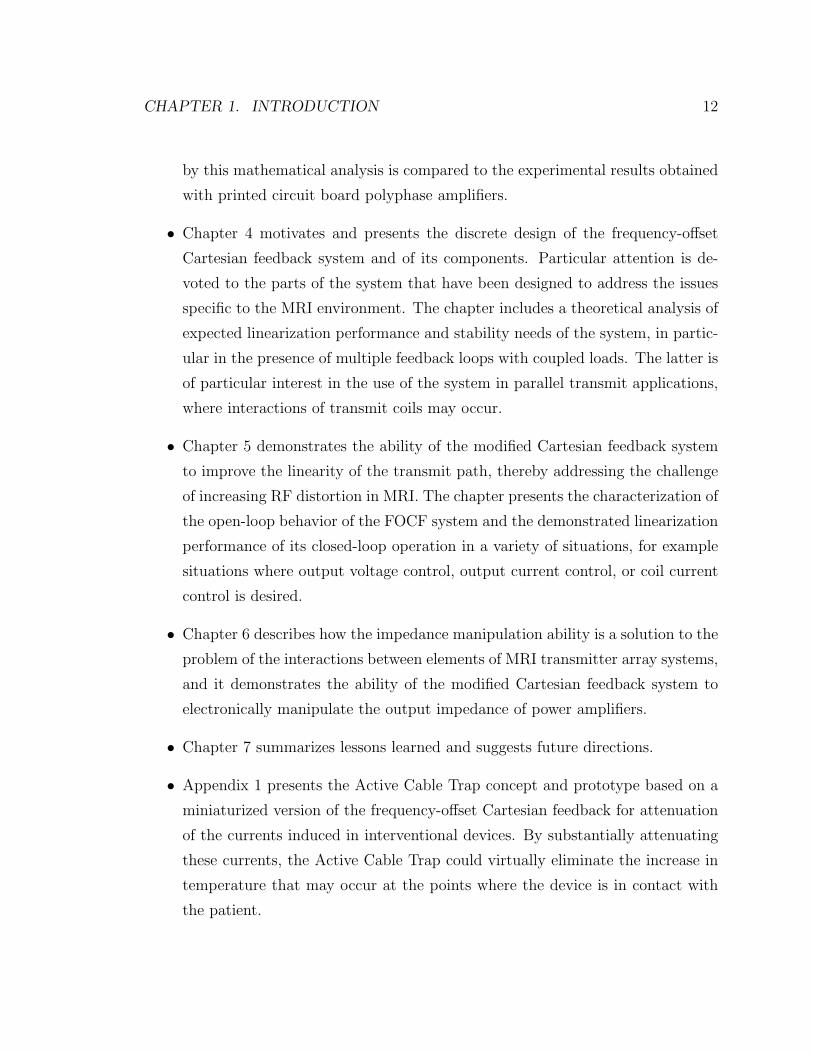
• Appendix 1 presents the Active Cable Trap concept and prototype based on a
miniaturized version of the frequency-offset Cartesian feedback for attenuation
of the currents induced in interventional devices. By substantially attenuating
these currents, the Active Cable Trap could virtually eliminate the increase in
temperature that may occur at the points where the device is in contact with
the patient.

Chapter 2
Cartesian Feedback
2.1 Introduction
This chapter describes the classic Cartesian feedback method. It motivates the choice
of this particular linearization technique for application in MRI over alternative meth-
ods, which are used in communications to deal with the problem of distortion intro-
duced by the RF power amplifiers.
The problems of the traditional Cartesian feedback method are also described.
These problems are the sensitivity of this technique to LO-leakage and quadrature
mismatches. The implementation of a low-frequency complex baseband amplification
of the feedback loop error is then presented as a solution to the latter.
Finally, this chapter introduces the main issues specific to the MRI environment
that need to be addressed for the successful application of Cartesian feedback in this
field.
2.2 Cartesian Feedback
2.2.1 Brief History
Cartesian feedback control was invented in the early 1980s by Petrovic [63] to address
the problem of distortion introduced by RF-power amplifiers used in high-frequency
13
CHAPTER 2. CARTESIAN FEEDBACK 14
transmitters for communications. In communications, RF power amplifiers are used
in a variety of applications including radio and TV transmitters, wireless communi-
cations, and satellite communication systems. While high-linearity power amplifiers
are generally available, these are also characterized by low efficiency, which poses
problems such as high RF dissipation and thus heating, high costs, and difficulty of
integration of these devices. In communications, the application of Cartesian feedback
to a higher-efficiency amplifier allows one to relax the trade-off between linearization
and efficiency and to obtain acceptably low distortion during transmission.
Despite its potential for application in the field, the popularity of the invention was
held back by complexities associated with the actual implementation of the system.
Only in the mid 1990s, thanks to the progress made in the field of analog integrated
electronics, did Cartesian feedback become a topic of intense study and development.
From 1991 to 1994, Johansson and Mattsson demonstrated the flexibility of the
technique with applications in the linearization of RF power amplifiers for personal
communication networks, [35], linear TDMA modulation [36], and multi-carrier com-
munication systems [37, 38]. During those same years, Briffa and Faulkner focused
most of their studies and implementation efforts on solving the problems of stability of
Cartesian feedback, taking in consideration the non-idealities of the actual implemen-
tation of the system [9–12, 24, 25]. In 1996, Boolorian and McGeehan published new
solutions for maximizing the linearization bandwidth [6], new compensation strate-
gies [7], and new applications [4, 5, 8]. In 1997, Kenington for the first time studied
the noise performance of a Cartesian loop transmitter [41]. More recently, Dawson
and Lee implemented the first fully integrated Cartesian feedback system for power
amplifier linearization [20]. Integrated solutions for Cartesian feedback linearization
were then developed by two manufacturers, namely CML Microelectronics (in 2007)
and Motorola (expected in 2010).
In the context of MRI, the Cartesian feedback technique first appeared in 2004
thanks to the work by Hoult, who proposed this technique as a solution to the problem
of coil interactions in an array of coils for the purpose of transmission in MRI [31–33].
CHAPTER 2. CARTESIAN FEEDBACK 15
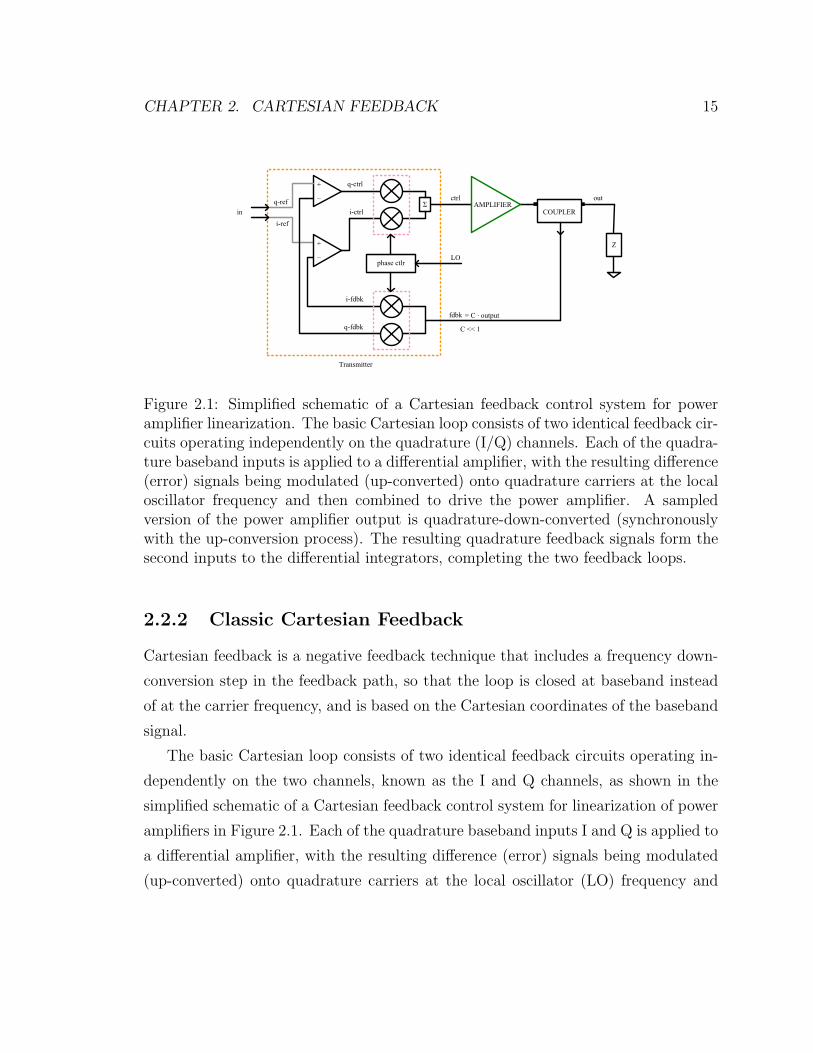
Figure 2.1: Simplified schematic of a Cartesian feedback control system for poweramplifier linearization. The basic Cartesian loop consists of two identical feedback cir-cuits operating independently on the quadrature (I/Q) channels. Each of the quadra-ture baseband inputs is applied to a differential amplifier, with the resulting difference(error) signals being modulated (up-converted) onto quadrature carriers at the localoscillator frequency and then combined to drive the power amplifier. A sampledversion of the power amplifier output is quadrature-down-converted (synchronouslywith the up-conversion process). The resulting quadrature feedback signals form thesecond inputs to the differential integrators, completing the two feedback loops.
2.2.2 Classic Cartesian Feedback
Cartesian feedback is a negative feedback technique that includes a frequency down-
conversion step in the feedback path, so that the loop is closed at baseband instead
of at the carrier frequency, and is based on the Cartesian coordinates of the baseband
signal.
The basic Cartesian loop consists of two identical feedback circuits operating in-
dependently on the two channels, known as the I and Q channels, as shown in the
simplified schematic of a Cartesian feedback control system for linearization of power
amplifiers in Figure 2.1. Each of the quadrature baseband inputs I and Q is applied to
a differential amplifier, with the resulting difference (error) signals being modulated
(up-converted) onto quadrature carriers at the local oscillator (LO) frequency and
CHAPTER 2. CARTESIAN FEEDBACK 16
Vcm
Vcm
ir
Q
I
if
qr
qf
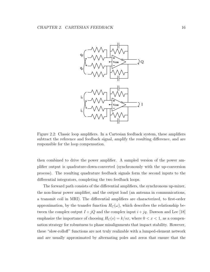
Figure 2.2: Classic loop amplifiers. In a Cartesian feedback system, these amplifierssubtract the reference and feedback signal, amplify the resulting difference, and areresponsible for the loop compensation.
then combined to drive the power amplifier. A sampled version of the power am-
plifier output is quadrature-down-converted (synchronously with the up-conversion
process). The resulting quadrature feedback signals form the second inputs to the
differential integrators, completing the two feedback loops.
The forward path consists of the differential amplifiers, the synchronous up-mixer,
the non-linear power amplifier, and the output load (an antenna in communications,
a transmit coil in MRI). The differential amplifiers are characterized, to first-order
approximation, by the transfer function HC(ω), which describes the relationship be-
tween the complex output I+ jQ and the complex input i+ jq. Dawson and Lee [18]
emphasize the importance of choosing HC(s) = k/sx, where 0 < x < 1, as a compen-
sation strategy for robustness to phase misalignments that impact stability. However,
these “slow-rolloff” functions are not truly realizable with a lumped-element network
and are usually approximated by alternating poles and zeros that ensure that the
CHAPTER 2. CARTESIAN FEEDBACK 17
-500 0 5000.20
0.32
0.50
0.79
1.26
2
Frequency (KHz)
Freq
uenc
y R
espo
nse,
Mag
nitu
de (V
/V)
-90
-45
0
45
90
Frequency Response, Phase (degree)
Freq. Response, AmplitudeFreq. Response, Phase
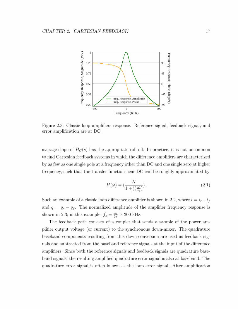
Figure 2.3: Classic loop amplifiers response. Reference signal, feedback signal, anderror amplification are at DC.
average slope of HC(s) has the appropriate roll-off. In practice, it is not uncommon
to find Cartesian feedback systems in which the difference amplifiers are characterized
by as few as one single pole at a frequency other than DC and one single zero at higher
frequency, such that the transfer function near DC can be roughly approximated by
H(ω) = (K
1 + j( ωωo
)). (2.1)
Such an example of a classic loop difference amplifier is shown in 2.2, where i = ir−ifand q = qr − qf . The normalized amplitude of the amplifier frequency response is
shown in 2.3; in this example, fo = ωo
2πis 300 kHz.
The feedback path consists of a coupler that sends a sample of the power am-
plifier output voltage (or current) to the synchronous down-mixer. The quadrature
baseband components resulting from this down-conversion are used as feedback sig-
nals and subtracted from the baseband reference signals at the input of the difference
amplifiers. Since both the reference signals and feedback signals are quadrature base-
band signals, the resulting amplified quadrature error signal is also at baseband. The
quadrature error signal is often known as the loop error signal. After amplification
CHAPTER 2. CARTESIAN FEEDBACK 18
and up-conversion, the two paths in quadrature are summed to form the control sig-
nal driving the power amplifier. Once the loop is closed and if the conditions for
stability are met, then the control signal is the pre-distorted version of the desired
reference signal needed to compensate for the distortion of the power amplifier. As
will be shown in Chapter 4,
errorbaseband ∝1
loopgain. (2.2)
Hence, for very high loop gain (ideally, infinite) the control law of the system is,
simply
feedbackbaseband ≈ referencebaseband (2.3)
and, correspondingly
outputRF ≈ referenceRF/C (2.4)
where C is the attenuation coefficient of the coupler sampling the output of the power
amplifier. In words, once the loop is closed and if the conditions for stability are met,
then for very high loop gain the output signal will be an exact replica of the reference
signal, translated to the RF band and amplified by 1/C.
The last indispensable component of a Cartesian feedback system is the phase
shifter. Synchronism between the up- and down-mixers is obtained by splitting a
common RF carrier (the local oscillator, or LO, frequency), however the different
phase rotation (phase shift) through the feedback and forward paths cause the refer-
ence and feedback signals to be phase misaligned, a situation that compromises the
stability of the system. The phase shifter is thus necessary to compensate for the
phase shift and maintain the relationship that guarantees the loop stability. In ad-
dition to phase shift between the up-converted and down-converted signals, a second
effect—time delay in the loop—limits stability. This effect is typical of any feedback
system and defines the bandwidth allowed within the loop and thus the amount of
linearization that can be applied over a given bandwidth [29].
The system comprising the loop error amplifiers, up- and down-conversion mixers,
and phase shifter is known as the transmitter of the Cartesian feedback system.
CHAPTER 2. CARTESIAN FEEDBACK 19
Cartesian feedback has received a great deal of attention in communications thanks
to its advantages over alternative methods: it does not require a detailed knowledge
of the power amplifier behavior and is immune to changes such as those due to
temperature and aging. Moreover, it is suitable for almost any type of modulation
of the reference signal, including those characterized by a substantial variation in the
signal envelope as measured by the peak-to-average ratio (PAR). However, the classic
Cartesian feedback architecture is not immune to problems. Since both the reference
and feedback signals and the amplification of the loop error signals occur at baseband,
the transmitter of the system must be designed with tight specifications regarding the
matching between the two quadrature paths. Mismatches between these two paths
can create undesired frequencies that also are within the bandwidth of amplification
of the loop error signal (aka, the control loop bandwidth) and thus appear at the
output of the power amplifier.
2.2.3 Problems of Classic Cartesian Feedback
Designers of Cartesian feedback systems face two practical challenges when imple-
menting the system transmitter: minimizing the mismatches between amplitude and
phase of the two quadrature signals, and minimizing the differences between the volt-
age and current settings of their two paths at the zero frequency (DC).
Mismatches between amplitude and phase of the two quadrature signals will cre-
ate an image of the desired signal, that is, an undesired frequency component of the
signal spectrum at the opposite side of the carrier (LO). This is known as “quadrature
mismatch.” For a classic Cartesian feedback transmitter, whose loop error amplifica-
tion is at baseband (symmetric around DC), the image will always be in the control
loop bandwidth. Image suppression of 40 dB is desirable but very difficult to achieve.
One of the two limits to obtaining good image suppression is in producing accurate
quadrature reference baseband signals. Petrovic has shown that considerable effort
was expended on finding solutions to this problem. Although excellent results were
achieved, this was at the expense of increased cost and complexity. The availability
CHAPTER 2. CARTESIAN FEEDBACK 20
of low cost, high performance Digital Signal Processors (DSPs) and Digital to Ana-
logue Converters (DACs) provides a solution to this problem. The second limit is in
producing accurate quadrature feedback baseband signals at the output of the Carte-
sian feedback down-converter. The down-converter inevitably suffers from amplitude
and phase inaccuracies for which, again, only expensive and complex solutions can
compensate.
To understand how undesired frequencies are created in the output spectrum by
quadrature errors, an open-loop analysis of the circuit is useful. Consider the case of
the loop open at the output of the down-mixer. Let the power amplifier be a perfect,
ideal amplification block of gain G. The baseband feedback complex signals, if (t) and
qf (t), appear at the down-mixer output as a result of input reference signals ir(t) and
qr(t) of time-varying envelope A(t) and modulation frequency ωB. If the up-mixer is
error-free and the down-mixer introduces a phase quadrature error φ, then
if (t) = KGA(t) cos(ωBt−φ
2) (2.5)
qf (t) = KGA(t) sin(ωBt+φ
2) (2.6)
that is, the overall feedback signal Sf is
Sf (t) = if (t) + jqf (t) = KGA(t)
(ej(ωB)t cos(
φ
2) + jej(−ωB)t sin(
φ
2)
). (2.7)
If φ is zero, then Sf contains only the desired frequency +ωB; otherwise, a so-called
image (or, ghost) frequency −ωB is also produced before the subtraction node. Since
the non-ideality responsible for this unwanted behavior is in the feedback path, it
will not be compensated by the loop operation. It can be shown that for the image
rejection ratio (the ratio of the amplitudes of the desired and image frequencies) to
be at least 40 dB, the maximum value of the phase error φ must be 1.15. Similarly,
the maximum value of amplitude imbalance to obtain the same image rejection ratio
is 2%.
As with the case of amplitude and quadrature mismatches, differences between
the DC settings of the quadrature path (known as DC offset) will create an undesired

CHAPTER 2. CARTESIAN FEEDBACK 21
frequency component of the signal spectrum exactly at the carrier (LO) known as
“LO leakage.” Operational amplifiers within the system have DC offsets that drift
with temperature, and the down-converter mixers produce a frequency dependent
DC offset. In addition, 1f
noise drops below thermal noise above 100 Hz to 100 kHz
(depending on the technological process) and is thus a problem near DC. For these
reasons, at least 40 dB of DC offset correction is desirable. The typical method of
carrier suppression is to use sample-and-hold devices to null out the closed loop DC
offset. This solution, once again, adds complexity and cost to the implementation.
It is also possible to use a DSP to measure the DC offsets and to digitally predistort
the I-Q drive to the transmitter. However, this method eliminates fewer DC offsets.
Anticipating the application of Cartesian feedback in MRI, the undesired quadra-
ture mismatches and LO leakage in the RF transmit field would create artifacts to
appear in the final image, which would compromise the diagnostic information con-
tained in the image. The classic approach to Cartesian feedback would require that
the transmitter meet the very tight specification on amplitude and phase mismatches
and DC offset. A better solution is to offset the reference signal, feedback signal, and
loop error amplification of the classic Cartesian feedback system away from baseband,
to only one side of the carrier, so that both the quadrature mismatches and LO leak-
age would be outside the control bandwidth. This solution is accessible, thanks to
the use of polyphase amplifiers.
2.2.4 Towards a Modified Cartesian Feedback Architecture
While there is a strong theoretical motivation to pursue Cartesian feedback, its adop-
tion has been held back by the complexities associated with the actual implementation
of the system as explained in Section 2.2.3. Issues such as the impact of phase mis-
alignment on stability, phase and amplitude quadrature errors (particularly in the
down-converter of the feedback path), and DC offsets (particularly at the output of
the multipliers and at the input of the loop error amplifiers) have been and still are the
subject of many studies. The limit imposed by the accuracy of the down-conversion
is fundamental to linearization strategies, as errors in the feedback path cannot be
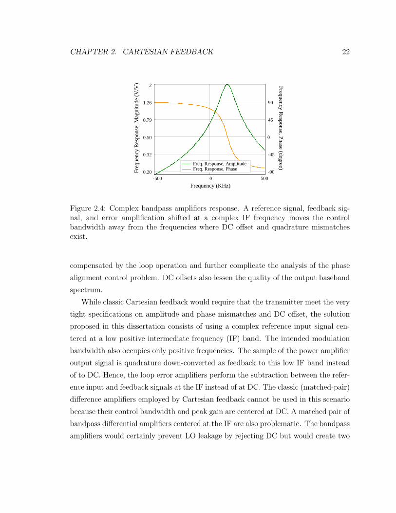
CHAPTER 2. CARTESIAN FEEDBACK 22
-500 0 500Frequency (KHz)
Freq
uenc
y R
espo
nse,
Mag
nitu
de (V
/V)
0.20
0.32
0.50
0.79
1.26
2
-90
-45
0
45
90
Frequency Response, Phase (degree)Freq. Response, Amplitude
Freq. Response, Phase
Figure 2.4: Complex bandpass amplifiers response. A reference signal, feedback sig-nal, and error amplification shifted at a complex IF frequency moves the controlbandwidth away from the frequencies where DC offset and quadrature mismatchesexist.
compensated by the loop operation and further complicate the analysis of the phase
alignment control problem. DC offsets also lessen the quality of the output baseband
spectrum.
While classic Cartesian feedback would require that the transmitter meet the very
tight specifications on amplitude and phase mismatches and DC offset, the solution
proposed in this dissertation consists of using a complex reference input signal cen-
tered at a low positive intermediate frequency (IF) band. The intended modulation
bandwidth also occupies only positive frequencies. The sample of the power amplifier
output signal is quadrature down-converted as feedback to this low IF band instead
of to DC. Hence, the loop error amplifiers perform the subtraction between the refer-
ence input and feedback signals at the IF instead of at DC. The classic (matched-pair)
difference amplifiers employed by Cartesian feedback cannot be used in this scenario
because their control bandwidth and peak gain are centered at DC. A matched pair of
bandpass differential amplifiers centered at the IF are also problematic. The bandpass
amplifiers would certainly prevent LO leakage by rejecting DC but would create two
CHAPTER 2. CARTESIAN FEEDBACK 23
control bands for complex signals centered at the positive and negative IF frequen-
cies. Quadrature image errors would remain. More importantly, because two high
gain control bands are generated, the system is potentially unstable as the desired sig-
nal and its quadrature mismatches experience different loop phase rotation and hence
demand different compensation strategies. The optimal solution to the problem of
subtracting the reference input and the feedback signal would be a complex bandpass
difference amplifier, which would create a single control bandwidth centered at the
positive IF only. In the realm of quadrature signals, a complex passband amplifier
does exist and can be synthesized with “active polyphase amplifiers.” The key mod-
ification to the classic Cartesian feedback control loop thus consists of substituting
active polyphase difference amplifiers for the classic matched difference amplifiers of
the Cartesian feedback system. The net result of this change is to move the loop con-
trol bandwidth away from DC (at baseband) and from the local oscillator frequency
(at RF), as shown in Figure 2.4, so that the undesired frequencies that would be
created by both quadrature errors and DC offsets are outside this bandwidth. With
this solution, even if quadrature errors and offsets within the loop are not stringently
minimized, they do not impair the performance of the Cartesian feedback system.
2.2.5 Adapting Cartesian Feedback to Application in MRI
In addition to using polyphase amplifiers in place of the classic baseband amplifiers
for the loop error amplification, developing a Cartesian feedback-controlled power
amplifier system for applications in MRI involves meeting the power, frequency, lin-
earity, and safety requirements of the latter, as well as creating solutions to address
issues that are not found in communications, where this technique was invented, and
that are specific to the MRI environment.
In particular, the power and frequency requirements of the system applied to
the MRI RF power amplifier are substantially different from those of the system
applied to the RF amplifier in communications. Moreover, the robustness of the
system is imperative for application in MRI, since the system controls the powerful
RF amplifiers driving the transmit coils.

CHAPTER 2. CARTESIAN FEEDBACK 24
In addition to meeting the above requirements, the implementation of the Carte-
sian feedback transmitter must include circuits to adapt the real signals employed
in MRI to the quadrature representation of both reference and feedback signals. For
example, the reference generation circuitry must convert the MRI signal into a pair of
(very well matched) reference quadrature signals. Similarly, the feedback path must
contain the circuitry necessary to generate the feedback quadrature signals from a
sample of the real signal at the output of the power amplifier.
2.3 Alternatives to Cartesian Feedback
The choice of Cartesian feedback for application to the field of MRI is warranted for a
number of reasons, which can be best appreciated when the technique is compared to
the available alternative methods of linearization of RF power amplifiers [40]. These
methods include (1) power back-off, (2) polar feedback, (3) feed-forward, and (4)
predistortion or iterative predistortion.
1. Power Back-Off. When high-linearity is needed but sophisticated linearization
techniques are not available, the simplest approach is to use the amplifier in
its most linear region, that is, to operate the amplifier at output powers much
lower than the maximum available. This approach is known as power back-off,
and the basic principle can be seen by looking at the characteristic equation
that describes the output envelope of any power amplifier as a function of the
input amplitude Vin and a series of coefficients:
Vout = a1Vin + a2V2in + a3V
3in + a4V
4in + . . . (2.8)
If Vin is small, the linear term with coefficient a1 is dominant. The main problem
with this approach is that the efficiency of an amplifier with power back-off will
be considerably lower than its maximum efficiency, which is obtained at full
power. Underutilizing the technology is one very expensive solution to the
problem at hand.
CHAPTER 2. CARTESIAN FEEDBACK 25
2. Polar Feedback. A polar feedback loop transmitter uses two feedback loops
from the output of the power amplifier, one for the amplitude and the other
for the phase of the transmitted signal. Amplitude-to-amplitude distortion is
corrected by the amplitude loop; amplitude-to-phase distortion, by the phase
feedback loop. The input signal to the power amplifier is the output of a Voltage
Controlled Oscillator (VCO), phase modulated and with constant amplitude.
The amplitude modulation is added at the output by varying the RF signal gain
of the amplifier. Because the polar-loop transmitter does not use up-conversion
in the RF chain, the need to suppress conversion images is obviated [80]. This
intrinsic advantage has drawbacks, however: the architecture needs a high-
quality dynamic VCO and a high-bandwidth envelope detector in the feedback
path, and it is not applicable to all modulation schemes.
3. Feed-Forward. A feed-forward amplifier consists of two loops: a signal cancel-
lation loop followed by an error cancellation loop. In the signal cancellation
loop a sample of the main amplifier output, attenuated by a factor matching
precisely the gain of the main amplifier, is subtracted from the properly delayed
version of the input. By accurately choosing the attenuation factor and input
delay, one ensures that the resulting signal contains only the distortion informa-
tion from the main amplifier; ideally, none of the input energy remains. In the
error-cancellation loop, this signal is linearly amplified by a secondary amplifier
and injected in anti-phase to a delayed version of the main amplifier output. At
the output of the feed-forward amplifier, only the ideally amplified version of
the input appears. The major advantage of a feed-forward amplifier is the lack
of a feedback loop, which means stability is not an issue: wideband operation
is guaranteed with significant linearity improvement. Drawbacks of this archi-
tecture are the need to accurately align the delays of the signal-cancellation
and error-cancellation loops, the sensitivity to gain and phase variations of the
secondary amplifier, and the generally poor efficiency.
4. Predistortion. A look-up table (LUT) that captures the inverse of the amplifier
nonlinear behavior precedes the amplifier itself, to ensure that the cascade of the
CHAPTER 2. CARTESIAN FEEDBACK 26
two is linear. Training of the LUT relies on feedback and adaptative algorithms,
based on accurate modeling of the amplifier. Because the system is based on
knowing and mathematically inverting the amplifier non-linearity, complexity
and cost are not trivial. The architecture is also limited by the inability to
account for changes in the amplifier behavior, such as thermal drift, unless the
LUT is updated often (Iterative Predistortion). Incidentally, Cartesian feedback
has been proposed for LUT training of digital predistortion systems [16].
In comparison to all of the above techniques, a frequency-offset Cartesian feedback
has a number of advantages that make it ideal for application to MRI:
1. No need for a dynamic, fast VCO/PLL to track the rapid phase changes which
can occur in some high-bandwidth RF envelopes found in MRI. In addition,
the PLL arrangement (such as in a polar loop) can have problems tracking or
locking at low-envelope levels, such as those occurring when the MRI signal
envelope passes through zero. A sinc pulse is a classic example.
2. The modulation signal is reduced to a simple mixer. The need for a separate
modulator at the final output RF is eliminated.
3. Simplicity of implementation. (In particular with the use of polyphase ampli-
fiers, which substantially relax the specifications of the transmitter compared
to the classic architecture.)
4. Applicable to any type of RF pulse envelope and any type of envelope modula-
tion.
5. A flexible approach to the choice of signal to be sampled at the output of the
RF power amplifier. We will see that, for example, sampling of the output
voltage, output current, or combination of the two, can be obtained without
substantially altering the hardware configuration.
Instead of linearizing efficient amplifiers, an alternative view is to boost the effi-
ciency of conventional linear amplifiers. A number of these efficiency-boosting power
CHAPTER 2. CARTESIAN FEEDBACK 27
amplification techniques exist and are often described as performing amplifier lin-
earization, when in fact they simply overcome the efficiency obstacle to the utiliza-
tion of already linear amplifiers. Examples of these techniques are (1) Doherty archi-
tecture, (2) envelope elimination and restoration, and (3) linear amplification with
non-linear components.
1. A very popular example is the Doherty technique. The basic idea behind the
Doherty technique is to allow one amplifier to operate at its peak envelope
power level, where its efficiency is maximum but its capability to deal with the
modulation peaks is very poor, while a second linear amplifier works in parallel
to faithfully reproduce the modulation peaks. When the input power is low, the
first amplifier acts alone and the second is shut off by drive control circuitry.
Other methods track the signal envelope level, to vary the standing DC bias on
a low-efficiency, high-linearity amplifier as a way to compensate for the loss of
efficiency caused by the use of back-off (Adaptative Bias), or manipulate the
reference signal to reduce its peak to r.m.s. amplitude (Crest Factor Reduction).
2. Envelope Elimination and Restoration (EER). EER involves signal processing
to radically alter the original signal. It is essentially a high-level modulation
technique, and as such may be implemented as either a complete linear trans-
mitter or as an RF amplifier. In this technique, the input signal, which may
contain both amplitude and phase modulation, is split to form a baseband
path containing the envelope of the input signal and an RF path containing a
constant-envelope modulated carrier signal. The latter is then amplified by a
high-efficiency RF amplifier, which will transmit the phase modulation infor-
mation to the output of the system. The baseband envelope signal is amplified
by an audio amplifier which modulates the power supply of the RF power stage.
If the delays of the two paths are properly matched, this modulation process
restores the signal envelope and results in a high-power replica of the input
being produced at the output. In EER, phase matching between the two sig-
nal paths is critical, and restoring the envelope in a power-efficient way is very
challenging.
CHAPTER 2. CARTESIAN FEEDBACK 28
3. Linear Amplification with Non-linear Components. The input signal is split
into two constant-envelope, phase-modulated signals by the signal separation
or generation process, and each is fed to its own non-linear RF power amplifier.
The two amplifiers increase the power of each signal by an identical amount. The
two signals are then summed in a quadrature combiner resulting in an amplified
version of the original signal that has, ideally, no added distortion. The key
barrier to the acceptance of this technique, also called “outphasing amplifier”
is obtaining good power combining with both low loss and high isolation.
Since they are not, strictly speaking, linearization techniques, these efficiency-
boosting techniques are not alternatives to the use of frequency-offset Cartesian feed-
back; they may, however, be used in conjunction with the latter, as a way to further
increase the efficiency of the Cartesian feedback-linearized RF power amplifier.
2.4 Summary
In Chapter 2, the architecture of classic Cartesian feedback has been introduced.
Alternatives to the use of this RF power amplifier linearization technique have also
been presented, and the choice of this particular method for application to MRI has
been motivated. As a solution to the problem of the high sensitivity of this method to
quadrature mismatches and DC offsets, which can create undesired frequencies at the
output of the power amplifier, the use of low-IF reference signals, feedback signals,
and loop error amplification bandwidth is proposed. In particular, a complex low-IF
control bandwidth can be obtained with the use of polyphase amplifiers. Chapter 3
is entirely dedicated to this particular and little-known class of amplifiers.
Chapter 3
Active Polyphase Amplifiers
3.1 Introduction
The successful implementation of a frequency-offset Cartesian feedback system is
based on the availability of complex-passband gain to selectively amplify the fre-
quencies of the feedback signal while rejecting the carrier and image frequencies. An
example of an electrical circuit with this characteristic gain is an active polyphase
amplifier. After a brief historical introduction and description of the requirements
of polyphase amplifiers for Cartesian feedback applications in MRI, this chapter in-
troduces the architecture and qualitative behavior of active polyphase amplifiers. A
mathematical analysis of the polyphase amplifier operation is then presented, with
the goal of demonstrating that satisfactory performance (in terms of rejection of un-
desired frequencies, bandpass center frequency, and bandwidth) can be achieved for
application of these circuits as the loop error amplifiers of frequency-offset Cartesian
feedback in MRI. The results of this analysis support those obtained in a series of
experiments, also described here.
3.2 Brief History
Active polyphase amplifiers, also known as active polyphase filters, are a recent in-
vention by Christopher Marshall of U.S. Philips Corporation [55]. In his U.S. patent
29
CHAPTER 3. ACTIVE POLYPHASE AMPLIFIERS 30
number 4,723,318 published in 1988, Marshall provides the first available description
of these circuits:
An active polyphase filter [is an] arrangement in which asymmetric
poles and zeros are obtained using feedback.
Active polyphase amplifiers did not receive any significant interest until the mid-
1990’s, when they were first used in the design of low-intermediate frequency (IF)
receivers in communications by Crols [18, 19], Chou [14], Linggajaya [53], and Not-
ten [60]. Used in an image-reject down-converter, the active polyphase filter imple-
mentation eliminated the needs or relaxed the requirements for the traditionally used
low-pass filter after quadrature down-conversion while providing gain.
In this dissertation, for the first time, active polyphase amplifiers support the key
modification to classic Cartesian feedback architecture that significantly relaxes the
specifications of the transmitter in terms of both quadrature mismatches and DC
offset.
3.3 Requirements
In the modified Cartesian feedback system, the complex reference input signal and
down-converted feedback signal are at a low positive IF band. The intended modula-
tion bandwidth also occupies only positive frequencies. Polyphase amplifiers replace
the classic amplifiers for the loop error amplification, in which amplification and sub-
traction between the reference input signals and feedback signals occur at this IF
instead of at DC. Contrary to a pair of bandpass amplifiers, they do so while creating
a single complex bandpass control bandwidth instead of two separate bandwidths at
both positive and negative frequencies (see Figure 3.1). The net result is to selectively
amplify the desired signals over quadrature mismatches and DC offsets, which relaxes
the specifications of the transmitter substantially.
The main characteristics of the complex bandpass control band are its bandwidth
and center frequency. The requirements regarding the latter depend on the partic-
ular application of the frequency-offset Cartesian feedback system; specifically, they
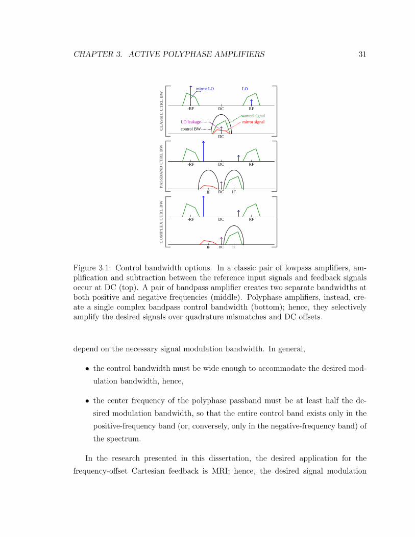
CHAPTER 3. ACTIVE POLYPHASE AMPLIFIERS 31
wanted signalmirror signal
LO
control BW
DC
DC
DC
RF
RF-RF
DC IF
DC RF-RF
-RF
IF
DC IFIF
LO leakage
CL
ASS
IC C
TR
L B
WPA
SSB
AN
D C
TR
L B
WC
OM
PLE
X C
TR
L B
W
mirror LO
Figure 3.1: Control bandwidth options. In a classic pair of lowpass amplifiers, am-plification and subtraction between the reference input signals and feedback signalsoccur at DC (top). A pair of bandpass amplifier creates two separate bandwidths atboth positive and negative frequencies (middle). Polyphase amplifiers, instead, cre-ate a single complex bandpass control bandwidth (bottom); hence, they selectivelyamplify the desired signals over quadrature mismatches and DC offsets.
depend on the necessary signal modulation bandwidth. In general,
• the control bandwidth must be wide enough to accommodate the desired mod-
ulation bandwidth, hence,
• the center frequency of the polyphase passband must be at least half the de-
sired modulation bandwidth, so that the entire control band exists only in the
positive-frequency band (or, conversely, only in the negative-frequency band) of
the spectrum.
In the research presented in this dissertation, the desired application for the
frequency-offset Cartesian feedback is MRI; hence, the desired signal modulation
CHAPTER 3. ACTIVE POLYPHASE AMPLIFIERS 32
bandwidth is that of the MRI RF pulse envelope. Typically, the latter is rarely above
20 kHz, though some very demanding MR strategies may require up to 100 kHz mod-
ulation. As a result, a polyphase amplification bandwidth at a center frequency of at
least 50 kHz must be demonstrated.
While perfect complex gain amplifiers would have zero overall response to the fre-
quency opposite (mirror) the desired frequency, in reality, even the ideal architecture
has a gain with finite roll-off with frequency, as will be shown below; therefore, it has
non-zero amplification at both DC and the mirror frequency of the desired signals.
For this reason, it is desirable to move the signal IF frequency band and thus the
center frequency of the polyphase amplifiers farther away from DC, so that the gain
will be significantly lower at both DC and the mirror frequency band than the gain
at the desired frequency band. In MRI, this consideration translates into a center
frequency ideally a decade higher than the minimum desired 50 kHz, that is, a 500
kHz or even higher center frequency should be demonstrated.
Besides the finite roll-off of the gain with frequency, other factors may cause the
polyphase amplifiers to respond to DC and opposite frequency. Imperfections of the
polyphase architecture cause both positive and negative frequencies to be amplified
as well as components of opposite frequency to be originated at the output. Whatever
the particular application may be, this consideration dictates an additional require-
ment for the practical polyphase amplifiers used in Cartesian feedback systems:
• the amplification of the desired positive frequencies (aka, the reference and
feedback signal) must be much higher than the amplification of the opposite
negative (image) frequencies (aka, the quadrature mismatches) created by the
loop imperfections.
The worst case scenario is that the quadrature mismatch image signal is as high
as the desired signal itself. In this catastrophic scenario, and for the specific case
of the application of the feedback system in MRI, a 40 dB differential amplification
would be considered adequate and values of 60 dB and over would be ideal.
To demonstrate that these performance requirements can be met in practical
implementations of polyphase amplifiers, a mathematical analysis of the polyphase
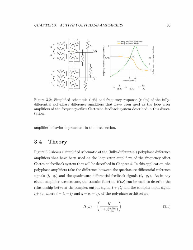
CHAPTER 3. ACTIVE POLYPHASE AMPLIFIERS 33
Vcm
Vcm
ir
Q
I
if
qr
qf
Ri RF
C
RC
+
−
+
−0
Frequency (kHz)
Freq
uenc
y R
espo
nse,
Mag
nitu
de (a
.u.)
0.7·K
K
-45
0
45
Frequency Response, Phase (degree)
Freq. Response, AmplitudeFreq. Response, Phase
ωc
ωc = RCC 1 ωo = RFC
1
ωo
K = Ri
RF
Figure 3.2: Simplified schematic (left) and frequency response (right) of the fully-differential polyphase difference amplifiers that have been used as the loop erroramplifiers of the frequency-offset Cartesian feedback system described in this disser-tation.
amplifier behavior is presented in the next section.
3.4 Theory
Figure 3.2 shows a simplified schematic of the (fully-differential) polyphase difference
amplifiers that have been used as the loop error amplifiers of the frequency-offset
Cartesian feedback system that will be described in Chapter 4. In this application, the
polyphase amplifiers take the difference between the quadrature differential reference
signals (ir, qr) and the quadrature differential feedback signals (if , qf ). As in any
classic amplifier architecture, the transfer function H(ω) can be used to describe the
relationship between the complex output signal I + jQ and the complex input signal
i+ jq, where i = ir − if and q = qr − qf , of the polyphase architecture:
H(ω) =
(K
1 + j(ω+ωc
ωo)
)(3.1)
CHAPTER 3. ACTIVE POLYPHASE AMPLIFIERS 34
where K, ωc, and ωo are the peak gain, center frequency, and half width of the
baseband signal band, respectively. H(ω) is the response of a single pole low pass
filter shifted by ωc away from 0 frequency as shown in Figure 3.2. It is as described
by 3.1 only if its active elements (such as the fully differential operational amplifiers
in the discrete implementation) are ideal blocks of infinite gain and bandwidth, its
passive components are perfectly matched, and the i and q input signals have the
same amplitude and are in perfect quadrature.
Qualitatively, the polyphase amplifier acts as two asymmetrically cross-coupled
amplifiers. The coupling from Q− i is the opposite sign of I − q. A quadrature ±90
degree phase relationship representing positive or negative input frequencies leads to
constructive or destructive interference in the outputs and to enhanced selectivity of
positive frequencies.
An equivalent representation of the operation of polyphase amplifiers can be ob-
tained if one considers the four real input (i, q) to real output (I, Q) transfer functions
and obtains the overall complex response by appropriately combining these functions.
For a unity-gain polyphase difference amplifier, these four equations are
i2I =I
i=
(ωojω− ω2
o
ω2
1
D
)(3.2)
q2I =I
q=
(+ωoωcω2
1
D
)(3.3)
q2Q =Q
q=
(ωojω− ω2
o
ω2
1
D
)(3.4)
i2Q =Q
i=
(−ωoωc
ω2
1
D
)(3.5)
where
D = 1− ω2o + ω2
c
ω2+
2ωojω
. (3.6)
This approach to polyphase amplifier analysis allows us to derive the equations that
separate the desired and undesired components of the output response, namely Up,
Vp, Um, Vm.

CHAPTER 3. ACTIVE POLYPHASE AMPLIFIERS 35
Up is the transfer function of the positive-frequency output to a positive-frequency
input complex signal,
Up = (i2I − jq2I) + j (i2Q− jq2Q) , (3.7)
Vp is the transfer function of the negative-frequency output to a positive-frequency
input (aka the “mirror” of the desired signal),
Vp = [(i2I − jq2I)∗ + j (i2Q− jq2Q)∗]∗, (3.8)
Vm is the transfer function of the negative-frequency output to a negative-frequency
input,
Vm = (i2I + jq2I)∗ + j (i2Q+ jq2Q)∗ , (3.9)
and finally Um is the transfer function of the positive-frequency output to a negative-
frequency input signal
Um = [(i2I + jq2I) + j (i2Q+ jq2Q)]∗ . (3.10)
When the ideal polyphase amplifier described by 3.1 is used as the difference amplifier
of a Cartesian feedback control system, the control bandwidth is frequency offset to
the positive axis; moreover in this ideal case, i2I = q2Q, and q2I = −i2Q such that
Vp = 0 and Um = 0.
Given a positive reference input frequency and an error-free down-mixer in the
control loop, the feedback input will always be composed of only positive frequencies,
and the only component of interest in the overall amplifier response is Up. However,
if the down-mixer (and other circuitry in the feedback path) introduces quadrature
mismatches and DC offsets, negative (mirror) frequencies and DC components will
also be generated at the feedback input of the polyphase difference amplifiers. In the
ideal architecture, where Vp = 0 and Um = 0, the amplification of these unwanted
frequencies originates from the spontaneous roll-off only of 3.1 in the negative fre-
quency band, described by Vm. To reduce this amplification (without affecting K),
the solution is simple and consists of increasing the center frequency ωc.
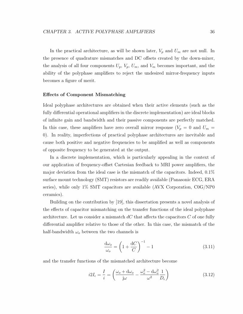
CHAPTER 3. ACTIVE POLYPHASE AMPLIFIERS 36
In the practical architecture, as will be shown later, Vp and Um are not null. In
the presence of quadrature mismatches and DC offsets created by the down-mixer,
the analysis of all four components Up, Vp, Um, and Vm becomes important, and the
ability of the polyphase amplifiers to reject the undesired mirror-frequency inputs
becomes a figure of merit.
Effects of Component Mismatching
Ideal polyphase architectures are obtained when their active elements (such as the
fully differential operational amplifiers in the discrete implementation) are ideal blocks
of infinite gain and bandwidth and their passive components are perfectly matched.
In this case, these amplifiers have zero overall mirror response (Vp = 0 and Um =
0). In reality, imperfections of practical polyphase architectures are inevitable and
cause both positive and negative frequencies to be amplified as well as components
of opposite frequency to be generated at the output.
In a discrete implementation, which is particularly appealing in the context of
our application of frequency-offset Cartesian feedback to MRI power amplifiers, the
major deviation from the ideal case is the mismatch of the capacitors. Indeed, 0.1%
surface mount technology (SMT) resistors are readily available (Panasonic ECG, ERA
series), while only 1% SMT capacitors are available (AVX Corporation, C0G/NP0
ceramics).
Building on the contribution by [19], this dissertation presents a novel analysis of
the effects of capacitor mismatching on the transfer functions of the ideal polyphase
architecture. Let us consider a mismatch dC that affects the capacitors C of one fully
differential amplifier relative to those of the other. In this case, the mismatch of the
half-bandwidth ωo between the two channels is
dωoωo
=
(1 +
dC
C
)−1
− 1 (3.11)
and the transfer functions of the mismatched architecture become
i2Iε =I
i=
(ωo + dωo
jω− ω2
o − dω2o
ω2
1
Dε
)(3.12)

CHAPTER 3. ACTIVE POLYPHASE AMPLIFIERS 37
q2Iε =I
q= +
(ωoωcω2− ωcdω
2o
ωoω2
)1
Dε
(3.13)
q2Qε =Q
q=
(ωo − dωo
jω− ω2
o − dω2o
ω2
1
Dε
)(3.14)
i2Qε =Q
i= −
(ωoωcω2− ωcdω
2o
ωoω2
)1
Dε
(3.15)
where
Dε = 1−ω2o + ω2
c − dω2o
(1 + ω2
c
ω2o
)ω2
+2ωojω
. (3.16)
It can be shown that, to first order approximation in case dC/C 1, the errors ε are
ε[i2I] = i2Iε − i2I ≈ +dωojω
1
D(3.17)
ε[q2I] = q2Iε − q2I ≈ 0 (3.18)
ε[q2Q] = q2Qε − q2Q ≈ −dωojω
1
D(3.19)
ε[i2Q] = i2Qε − i2Q ≈ 0 (3.20)
and thus the first-order errors to the desired and undesired baseband components of
the output response are
ε[Up] ≈ 0 (3.21)
ε[Vp] ≈(−2
dωojω
1
D
)∗(3.22)
ε[Vm] ≈ 0 (3.23)
ε[Um] ≈ −2dωojω
1
D(3.24)
which tells us that the polyphase amplifier with a small capacitive mismatch has
a desired response very close to that of the perfect amplifier. However, its mirror
response is not null anymore; moreover, since ε[Vp] is the complex conjugate of ε[Um],
the mirror response has even amplitude and odd phase.
This conclusion is validated by both simulations and experiments. As an example,
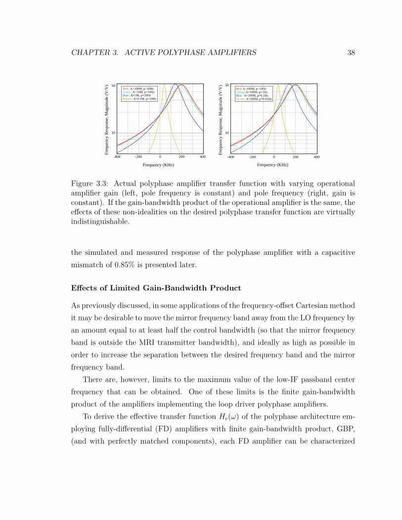
CHAPTER 3. ACTIVE POLYPHASE AMPLIFIERS 38
Frequency (KHz)
Freq
uenc
y R
espo
nse,
Mag
nitu
de (V
/V)
4002000-200-400
10
50Red : A=100M, p=10HzGreen : A=10M, p=10HzBlue : A=1M, p=10HzBrown : A=0.1M , p=10Hz
Freq
uenc
y R
espo
nse,
Mag
nitu
de (V
/V)
Frequency (KHz)
Red: A=100M, p=10HzGreen: A=100M, p=1HzBlue : A=100M, p=0.1HzBrown: A=100M , p=0.01Hz
4002000-200-400
10
50
Figure 3.3: Actual polyphase amplifier transfer function with varying operationalamplifier gain (left, pole frequency is constant) and pole frequency (right, gain isconstant). If the gain-bandwidth product of the operational amplifier is the same, theeffects of these non-idealities on the desired polyphase transfer function are virtuallyindistinguishable.
the simulated and measured response of the polyphase amplifier with a capacitive
mismatch of 0.85% is presented later.
Effects of Limited Gain-Bandwidth Product
As previously discussed, in some applications of the frequency-offset Cartesian method
it may be desirable to move the mirror frequency band away from the LO frequency by
an amount equal to at least half the control bandwidth (so that the mirror frequency
band is outside the MRI transmitter bandwidth), and ideally as high as possible in
order to increase the separation between the desired frequency band and the mirror
frequency band.
There are, however, limits to the maximum value of the low-IF passband center
frequency that can be obtained. One of these limits is the finite gain-bandwidth
product of the amplifiers implementing the loop driver polyphase amplifiers.
To derive the effective transfer function He(ω) of the polyphase architecture em-
ploying fully-differential (FD) amplifiers with finite gain-bandwidth product, GBP,
(and with perfectly matched components), each FD amplifier can be characterized

CHAPTER 3. ACTIVE POLYPHASE AMPLIFIERS 39
with analog behavior of finite DC gain, A, and finite bandwidth defined by the fre-
quency of a single pole, ωp; the transfer function of this behavior is shown in 3.25.
The GBP is, by definition, given by the product of A and ωp.
G(ω) =A
1 + j ωωp
. (3.25)
The next step is to solve the linear equation for the outputs Q, I as a function of
the inputs q, i. The following two new quantities can be defined in the process, the
magnitude factor M(ω) and shift factor S:
M(ω) = 1 +1 +K
A+ωcωp − ω2
Aωoωp= 1 +
(1 +K)A
GBP+ωcωp − ω2
GBPωo(3.26)
S(ω) = 1 +(1 +K)ωo + ωp + ωc
Aωp= 1 +
(1 +K)ωo + ωp + ωcGBP
. (3.27)
The effective transfer function He(ω) of the polyphase architecture employing FD
amplifier with finite GBP is
He(ω) =K
M(ω)
1
1 + jω−ωc
S
ωoM(ω)
S
(3.28)
in which ωec = ωc
Sis the effective passband center frequency, ωoc = ωo
M(ω)S
is the
effective half passband width, and Ke = KM(ω)
is the effective peak gain.
Figure 3.3 (left) shows the amplitude of the effective transfer function of a poly-
phase architecture of desired passband center frequency 200 kHz, desired half pass-
band width 80 kHz, and desired peak gain 50, with varying DC gain of the FD
amplifiers (A varies from 108 to 105): the finite bandwidth of the FD amplifiers was
held fixed at 10 Hz (ωp = 204π rads
). He(ω) in the case of A = 108 approximates the
ideal transfer function very well.
Similarly, Figure 3.3 (right) shows the amplitude of the effective transfer function
of the same polyphase architecture as a function, this time, of the pole frequency of
the FD amplifiers (from 10 to 0.01 Hz) while A is fixed and equal to 108.
The comparison of the two figures illustrates one of the key findings of this analysis:
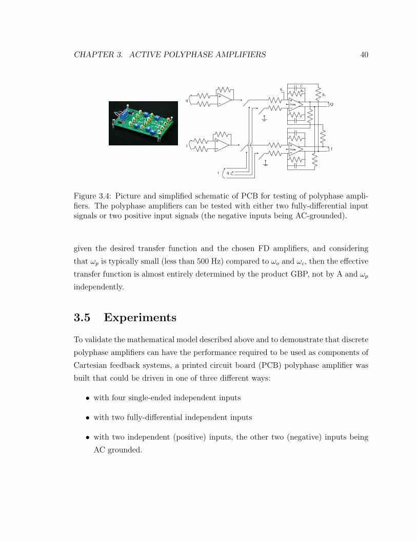
CHAPTER 3. ACTIVE POLYPHASE AMPLIFIERS 40
Vcm
Vcm
i
Q
Ii
q
q
Ri RF
C
RC
Figure 3.4: Picture and simplified schematic of PCB for testing of polyphase ampli-fiers. The polyphase amplifiers can be tested with either two fully-differential inputsignals or two positive input signals (the negative inputs being AC-grounded).
given the desired transfer function and the chosen FD amplifiers, and considering
that ωp is typically small (less than 500 Hz) compared to ωo and ωc, then the effective
transfer function is almost entirely determined by the product GBP, not by A and ωp
independently.
3.5 Experiments
To validate the mathematical model described above and to demonstrate that discrete
polyphase amplifiers can have the performance required to be used as components of
Cartesian feedback systems, a printed circuit board (PCB) polyphase amplifier was
built that could be driven in one of three different ways:
• with four single-ended independent inputs
• with two fully-differential independent inputs
• with two independent (positive) inputs, the other two (negative) inputs being
AC grounded.
CHAPTER 3. ACTIVE POLYPHASE AMPLIFIERS 41
Figure 3.5: Normalized real input (i, q) to real output (I, Q) simulated transferfunctions. The latter can be also measured by driving the PCB polyphase amplifierswith only one non-zero quadrature input signal (i or q) at a time.
A picture and a simplified schematic of this board is shown in Figure 3.4. The
board allowed bench testing of polyphase amplifiers built using discrete passive com-
ponents of known tolerance and discrete fully-differential amplifiers of known (nomi-
nal) GBP.
3.5.1 Results
The experiments described below were obtained by driving the polyphase amplifiers
with four single-ended independent inputs (i+, i−, q+, q−) and measuring the four
single-ended outputs elicited by each input (I+, I−, Q+, Q−). Appropriately com-
bining these 16 measurements allowed one to obtain the transfer functions i2I, i2Q,
q2I and q2Q, the output components Up, Um, Vp, and Vm, and their combination into
the overall desired and undesired responses.
The response of the discrete polyphase amplifiers was measured on the bench for
different values of capacitive matching as well as at different values of the center
frequency of the polyphase passband, and compared with the results of simulations
obtained using the mathematical model described in the previous sections.
In a first experiment, the components of the discrete polyphase circuit were sorted
in order to obtain 0.85% mismatch dCC
of the capacitors, peak gain of 40 dB, and
center frequency of nearly 200 kHz. Initially, the LT1994 fully differential discrete
operational amplifier by Linear Technology (with GBP of 70 MHz) was selected to
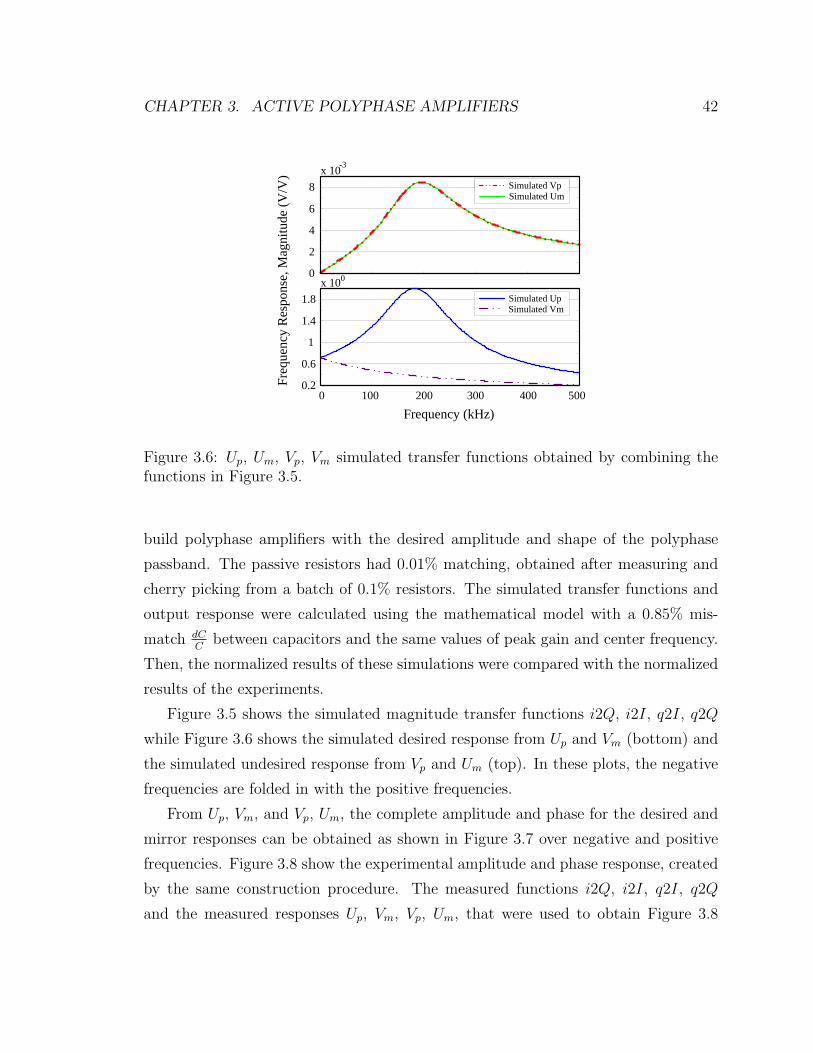
CHAPTER 3. ACTIVE POLYPHASE AMPLIFIERS 42
0
2
4
6
8x 10⁻³
0Fr
eque
ncy
Res
pons
e, M
agni
tude
(V/V
)
0 100 200 300 400 5000.2
0.6
1
1.4
1.8
Frequency (kHz)
x 10
Simulated VpSimulated Um
Simulated UpSimulated Vm
Figure 3.6: Up, Um, Vp, Vm simulated transfer functions obtained by combining thefunctions in Figure 3.5.
build polyphase amplifiers with the desired amplitude and shape of the polyphase
passband. The passive resistors had 0.01% matching, obtained after measuring and
cherry picking from a batch of 0.1% resistors. The simulated transfer functions and
output response were calculated using the mathematical model with a 0.85% mis-
match dCC
between capacitors and the same values of peak gain and center frequency.
Then, the normalized results of these simulations were compared with the normalized
results of the experiments.
Figure 3.5 shows the simulated magnitude transfer functions i2Q, i2I, q2I, q2Q
while Figure 3.6 shows the simulated desired response from Up and Vm (bottom) and
the simulated undesired response from Vp and Um (top). In these plots, the negative
frequencies are folded in with the positive frequencies.
From Up, Vm, and Vp, Um, the complete amplitude and phase for the desired and
mirror responses can be obtained as shown in Figure 3.7 over negative and positive
frequencies. Figure 3.8 show the experimental amplitude and phase response, created
by the same construction procedure. The measured functions i2Q, i2I, q2I, q2Q
and the measured responses Up, Vm, Vp, Um, that were used to obtain Figure 3.8
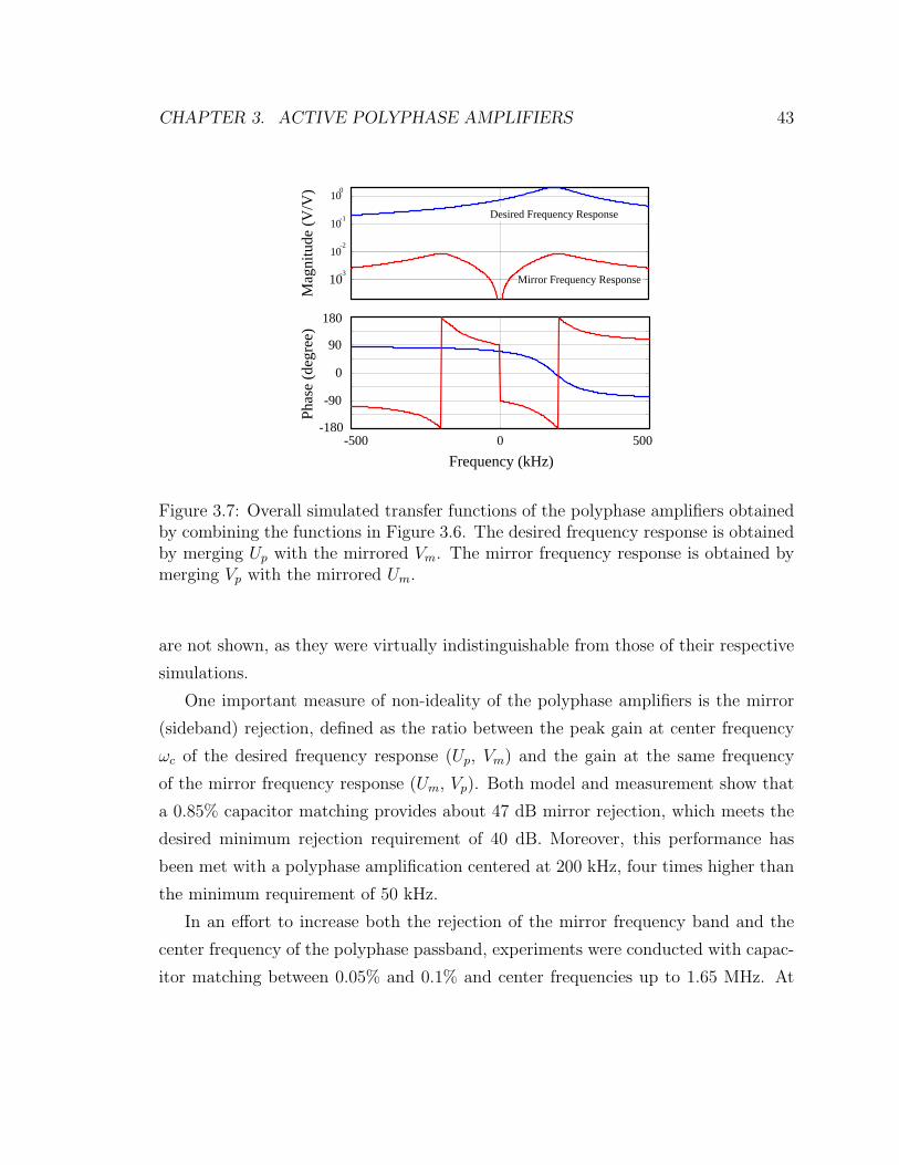
CHAPTER 3. ACTIVE POLYPHASE AMPLIFIERS 43
10-3
10-2
10-1
100
Mag
nitu
de (V
/V)
-90
0
90
-500 0 500Frequency (kHz)
Phas
e (d
egre
e)
-180
180
Desired Frequency Response
Mirror Frequency Response
Figure 3.7: Overall simulated transfer functions of the polyphase amplifiers obtainedby combining the functions in Figure 3.6. The desired frequency response is obtainedby merging Up with the mirrored Vm. The mirror frequency response is obtained bymerging Vp with the mirrored Um.
are not shown, as they were virtually indistinguishable from those of their respective
simulations.
One important measure of non-ideality of the polyphase amplifiers is the mirror
(sideband) rejection, defined as the ratio between the peak gain at center frequency
ωc of the desired frequency response (Up, Vm) and the gain at the same frequency
of the mirror frequency response (Um, Vp). Both model and measurement show that
a 0.85% capacitor matching provides about 47 dB mirror rejection, which meets the
desired minimum rejection requirement of 40 dB. Moreover, this performance has
been met with a polyphase amplification centered at 200 kHz, four times higher than
the minimum requirement of 50 kHz.
In an effort to increase both the rejection of the mirror frequency band and the
center frequency of the polyphase passband, experiments were conducted with capac-
itor matching between 0.05% and 0.1% and center frequencies up to 1.65 MHz. At
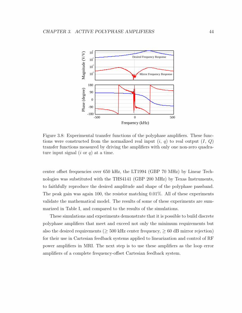
CHAPTER 3. ACTIVE POLYPHASE AMPLIFIERS 44
10-3
10-2
10-1
100
Mag
nitu
de (V
/V)
-500 0 500Frequency (kHz)
Phas
e (d
egre
e)
0
90
180
-90
-180
Desired Frequency Response
Mirror Frequency Response
Figure 3.8: Experimental transfer functions of the polyphase amplifiers. These func-tions were constructed from the normalized real input (i, q) to real output (I, Q)transfer functions measured by driving the amplifiers with only one non-zero quadra-ture input signal (i or q) at a time.
center offset frequencies over 650 kHz, the LT1994 (GBP 70 MHz) by Linear Tech-
nologies was substituted with the THS4141 (GBP 200 MHz) by Texas Instruments,
to faithfully reproduce the desired amplitude and shape of the polyphase passband.
The peak gain was again 100, the resistor matching 0.01%. All of these experiments
validate the mathematical model. The results of some of these experiments are sum-
marized in Table I, and compared to the results of the simulations.
These simulations and experiments demonstrate that it is possible to build discrete
polyphase amplifiers that meet and exceed not only the minimum requirements but
also the desired requirements (≥ 500 kHz center frequency, ≥ 60 dB mirror rejection)
for their use in Cartesian feedback systems applied to linearization and control of RF
power amplifiers in MRI. The next step is to use these amplifiers as the loop error
amplifiers of a complete frequency-offset Cartesian feedback system.
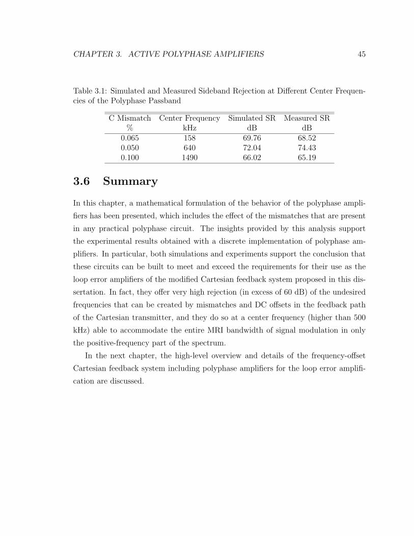
CHAPTER 3. ACTIVE POLYPHASE AMPLIFIERS 45
Table 3.1: Simulated and Measured Sideband Rejection at Different Center Frequen-cies of the Polyphase Passband
C Mismatch Center Frequency Simulated SR Measured SR% kHz dB dB
0.065 158 69.76 68.520.050 640 72.04 74.430.100 1490 66.02 65.19
3.6 Summary
In this chapter, a mathematical formulation of the behavior of the polyphase ampli-
fiers has been presented, which includes the effect of the mismatches that are present
in any practical polyphase circuit. The insights provided by this analysis support
the experimental results obtained with a discrete implementation of polyphase am-
plifiers. In particular, both simulations and experiments support the conclusion that
these circuits can be built to meet and exceed the requirements for their use as the
loop error amplifiers of the modified Cartesian feedback system proposed in this dis-
sertation. In fact, they offer very high rejection (in excess of 60 dB) of the undesired
frequencies that can be created by mismatches and DC offsets in the feedback path
of the Cartesian transmitter, and they do so at a center frequency (higher than 500
kHz) able to accommodate the entire MRI bandwidth of signal modulation in only
the positive-frequency part of the spectrum.
In the next chapter, the high-level overview and details of the frequency-offset
Cartesian feedback system including polyphase amplifiers for the loop error amplifi-
cation are discussed.

Chapter 4
System Design
4.1 Introduction
To improve the fidelity of the MRI RF transmit path and to electronically manipulate
the output impedance of the amplifiers driving transmit array coils, a frequency-offset
Cartesian feedback system has been designed and built.
This chapter discusses the design of the system. The motivations and high-level
objectives of the work, introduced in Chapter 1 and 2, are first revisited. Then, the
high-level system architecture and all its various parts are described in detail. Finally,
the system operation and linearization performance are analyzed and the conditions
necessary for the stability of the loop are discussed.
4.2 Motivations, Requirements and Objectives
As discussed in Chapter 1 and Chapter 2, a frequency-offset Cartesian feedback sys-
tem promises to address the challenges created by the recent trends in MRI, including
the trend toward higher frequencies and bandwidth, toward increasing use of trans-
mitter array systems, and toward increasing use of interventional devices. The main
challenges are distortion of the RF pulse envelope created by the MRI power amplifier,
interactions between the coils of transmitter array systems, and induced RF currents
in interventional devices, respectively. To address these challenges, frequency-offset
46
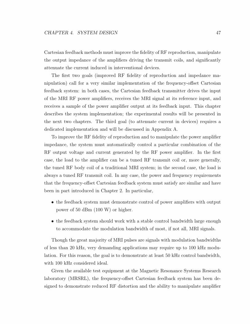
CHAPTER 4. SYSTEM DESIGN 47
Cartesian feedback methods must improve the fidelity of RF reproduction, manipulate
the output impedance of the amplifiers driving the transmit coils, and significantly
attenuate the current induced in interventional devices.
The first two goals (improved RF fidelity of reproduction and impedance ma-
nipulation) call for a very similar implementation of the frequency-offset Cartesian
feedback system: in both cases, the Cartesian feedback transmitter drives the input
of the MRI RF power amplifiers, receives the MRI signal at its reference input, and
receives a sample of the power amplifier output at its feedback input. This chapter
describes the system implementation; the experimental results will be presented in
the next two chapters. The third goal (to attenuate current in devices) requires a
dedicated implementation and will be discussed in Appendix A.
To improve the RF fidelity of reproduction and to manipulate the power amplifier
impedance, the system must automatically control a particular combination of the
RF output voltage and current generated by the RF power amplifier. In the first
case, the load to the amplifier can be a tuned RF transmit coil or, more generally,
the tuned RF body coil of a traditional MRI system; in the second case, the load is
always a tuned RF transmit coil. In any case, the power and frequency requirements
that the frequency-offset Cartesian feedback system must satisfy are similar and have
been in part introduced in Chapter 2. In particular,
• the feedback system must demonstrate control of power amplifiers with output
power of 50 dBm (100 W) or higher.
• the feedback system should work with a stable control bandwidth large enough
to accommodate the modulation bandwidth of most, if not all, MRI signals.
Though the great majority of MRI pulses are signals with modulation bandwidths
of less than 20 kHz, very demanding applications may require up to 100 kHz modu-
lation. For this reason, the goal is to demonstrate at least 50 kHz control bandwidth,
with 100 kHz considered ideal.
Given the available test equipment at the Magnetic Resonance Systems Research
laboratory (MRSRL), the frequency-offset Cartesian feedback system has been de-
signed to demonstrate reduced RF distortion and the ability to manipulate amplifier
CHAPTER 4. SYSTEM DESIGN 48
output impedance with various RF power amplifiers for 1.5 T MRI. However, the
system should work in any MRI system or Nuclear Magnetic Resonance (NMR) spec-
troscopy system of field strength from 1.5 T (64 MHz RF) up to 23 T (1 GHz RF)
with only minor modifications. This requirement on the Larmor frequency of the
MRI system translates into a technical specification for the operating frequency of
the control architecture:
• the feedback system must control any RF power amplifier between 64 MHz
(Larmor frequency at 1.5 T field strength) and 300 MHz (at 7 T), with only
minor modifications to the system architecture.
Finally, it is important that the phase shift that compensates the misalignment
between the up- and down-converted signals in the loop (see Chapter 2) can be studied
accurately and implemented rapidly before each use of the system. In fact, the correct
phase shift value depends on the behavior of the power amplifier and on the load,
and can differ greatly with the particular imaging system and imaging methodology.
Not only different amplifiers and loads could be used, but even given the same power
amplifier and load, the characteristic of the object being imaged (the patient) can
change the loaded Q and, consequently, the conditions for stability. In summary,
• the feedback system must support methods for the automatic measurement of
the phase loop rotation and automatic calibration of the phase shift necessary
for the system stability.
More specific objectives that motivated both the actual implementation choices
and the approach to its theoretical analysis have been:
1. to demonstrate a discrete prototype of a frequency-offset Cartesian feedback
power amplifier control system based on polyphase loop error amplifiers;
2. to demonstrate that both DC-coupling and AC-coupling of the control loop are
possible, and explore the trade-offs involved in choosing one approach versus
the other;

CHAPTER 4. SYSTEM DESIGN 49
3. to demonstrate the behavior of the control loop with different types of loads at
the power amplifier output, such as a 50 Ω dummy load, a loaded or unloaded
transmit coil element, and a bird cage body coil;
4. to demonstrate the behavior of the control loop with different gains for the
forward and feedback path;
5. to demonstrate the frequency range of stable operation at varying values of the
phase shift between the up- and down-conversion mixers;
6. to be able to change gain and phase characteristics of the loop using a PC
interface;
7. to demonstrate that frequency-offset Cartesian feedback works with any choice
of feedback signal obtained by sampling an arbitrary combination of the output
voltage and current of the power amplifier;
8. to demonstrate that the frequency-offset Cartesian feedback works with a feed-
back signal obtained by sampling the current in a transmit coil directly.
In the next sections, the frequency-offset Cartesian feedback architecture will be
described, with emphasis on the choices that enabled the above requirements and
objectives to be met.
4.3 High-Level System Preview
Figure 4.1 shows the basic hardware diagram of the frequency-offset Cartesian feed-
back system. In addition to the RF power amplifier, the basic blocks of the system
are:
1. a printed-circuit board (PCB) frequency-offset Cartesian feedback transmitter,
which will be referred to as “Genie”;
2. a load to the RF power amplifier, which can be a 50 Ω dummy load, a tuned
transmit coil, or an RF body coil;
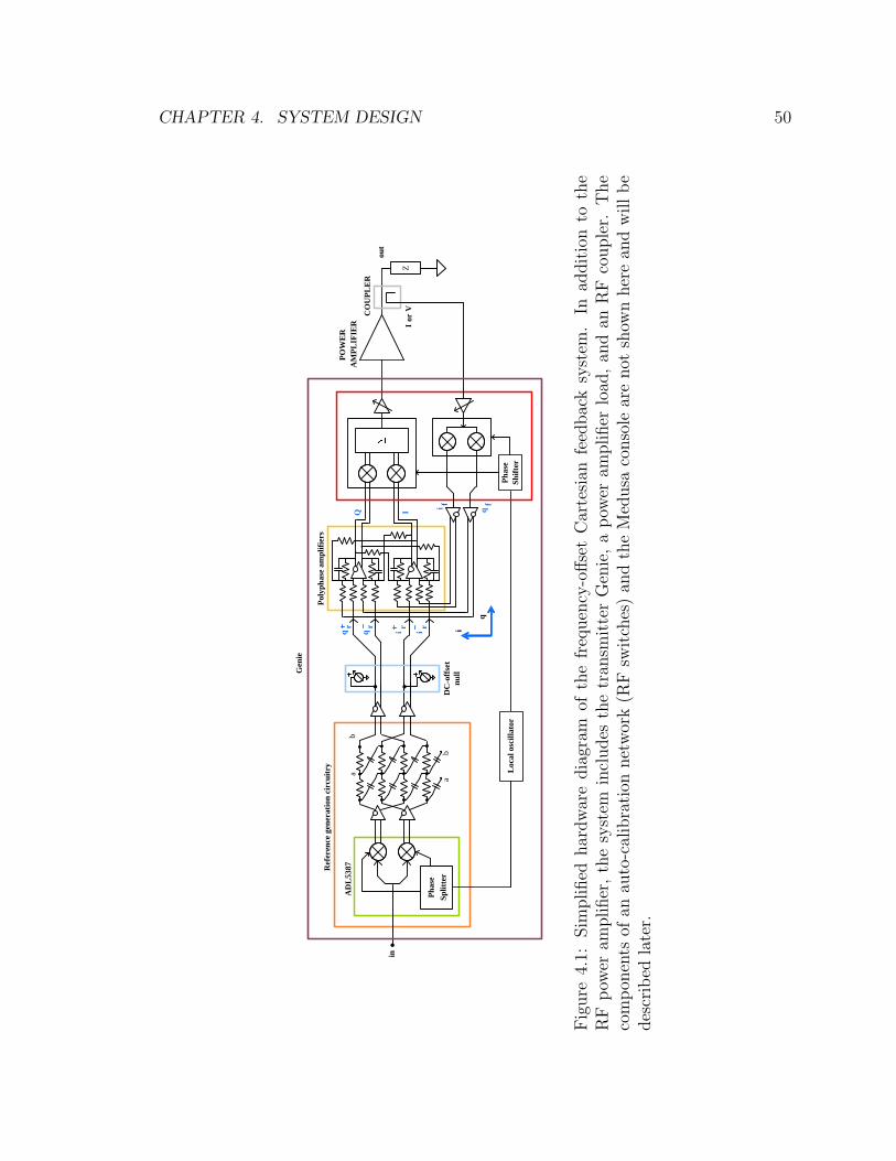
CHAPTER 4. SYSTEM DESIGN 50
POW
ER
A
MPL
IFIE
R
Poly
phas
e am
plifi
ers
Phas
eSh
ifter
Gen
ie
I or
VZ
CO
UPL
ER
qi ff
Q I
q
i
Phas
eSp
litte
r
in
AD
L53
87Ref
eren
ce g
ener
atio
n ci
rcui
try
ab
ab
DC
-off
set
null
q ir r
q ir r
Loc
al o
scill
ator
out
Fig
ure
4.1:
Sim
plified
har
dw
are
dia
gram
ofth
efr
equen
cy-o
ffse
tC
arte
sian
feed
bac
ksy
stem
.In
addit
ion
toth
eR
Fp
ower
amplifier
,th
esy
stem
incl
udes
the
tran
smit
ter
Gen
ie,
ap
ower
amplifier
load
,an
dan
RF
couple
r.T
he
com
pon
ents
ofan
auto
-cal
ibra
tion
net
wor
k(R
Fsw
itch
es)
and
the
Med
usa
conso
lear
enot
show
nher
ean
dw
ill
be
des
crib
edla
ter.
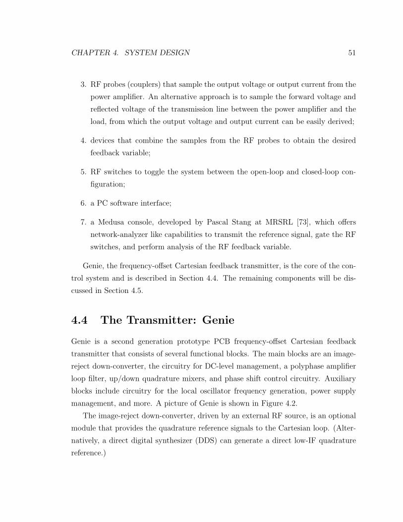
CHAPTER 4. SYSTEM DESIGN 51
3. RF probes (couplers) that sample the output voltage or output current from the
power amplifier. An alternative approach is to sample the forward voltage and
reflected voltage of the transmission line between the power amplifier and the
load, from which the output voltage and output current can be easily derived;
4. devices that combine the samples from the RF probes to obtain the desired
feedback variable;
5. RF switches to toggle the system between the open-loop and closed-loop con-
figuration;
6. a PC software interface;
7. a Medusa console, developed by Pascal Stang at MRSRL [73], which offers
network-analyzer like capabilities to transmit the reference signal, gate the RF
switches, and perform analysis of the RF feedback variable.
Genie, the frequency-offset Cartesian feedback transmitter, is the core of the con-
trol system and is described in Section 4.4. The remaining components will be dis-
cussed in Section 4.5.
4.4 The Transmitter: Genie
Genie is a second generation prototype PCB frequency-offset Cartesian feedback
transmitter that consists of several functional blocks. The main blocks are an image-
reject down-converter, the circuitry for DC-level management, a polyphase amplifier
loop filter, up/down quadrature mixers, and phase shift control circuitry. Auxiliary
blocks include circuitry for the local oscillator frequency generation, power supply
management, and more. A picture of Genie is shown in Figure 4.2.
The image-reject down-converter, driven by an external RF source, is an optional
module that provides the quadrature reference signals to the Cartesian loop. (Alter-
natively, a direct digital synthesizer (DDS) can generate a direct low-IF quadrature
reference.)
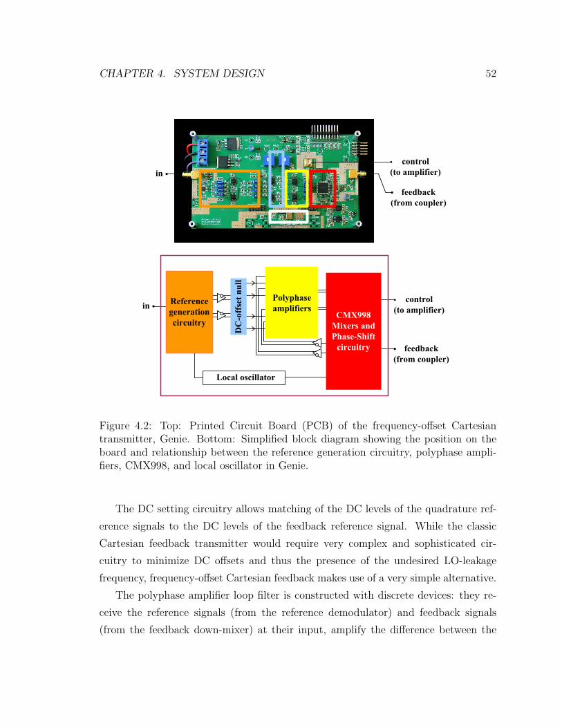
CHAPTER 4. SYSTEM DESIGN 52
PhaseShifter
Figure 4.2: Top: Printed Circuit Board (PCB) of the frequency-offset Cartesiantransmitter, Genie. Bottom: Simplified block diagram showing the position on theboard and relationship between the reference generation circuitry, polyphase ampli-fiers, CMX998, and local oscillator in Genie.
The DC setting circuitry allows matching of the DC levels of the quadrature ref-
erence signals to the DC levels of the feedback reference signal. While the classic
Cartesian feedback transmitter would require very complex and sophisticated cir-
cuitry to minimize DC offsets and thus the presence of the undesired LO-leakage
frequency, frequency-offset Cartesian feedback makes use of a very simple alternative.
The polyphase amplifier loop filter is constructed with discrete devices: they re-
ceive the reference signals (from the reference demodulator) and feedback signals
(from the feedback down-mixer) at their input, amplify the difference between the
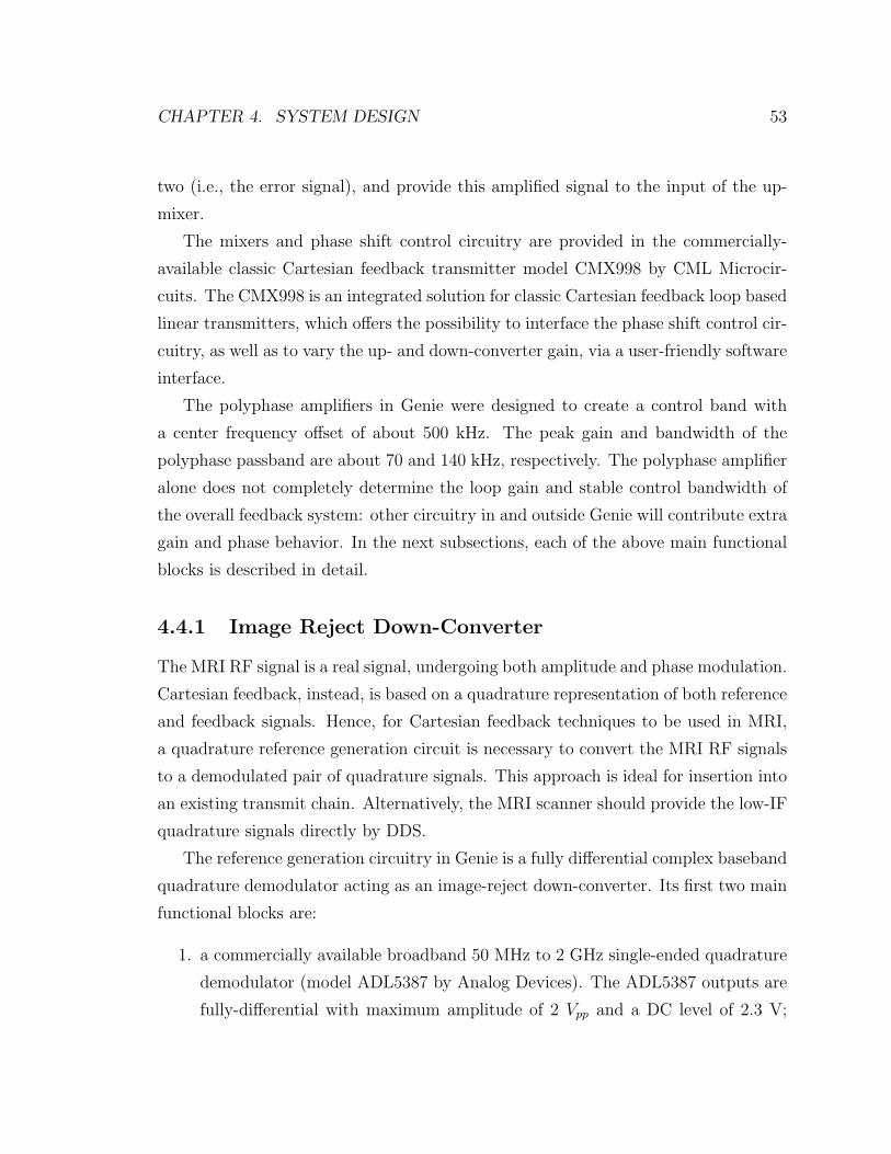
CHAPTER 4. SYSTEM DESIGN 53
two (i.e., the error signal), and provide this amplified signal to the input of the up-
mixer.
The mixers and phase shift control circuitry are provided in the commercially-
available classic Cartesian feedback transmitter model CMX998 by CML Microcir-
cuits. The CMX998 is an integrated solution for classic Cartesian feedback loop based
linear transmitters, which offers the possibility to interface the phase shift control cir-
cuitry, as well as to vary the up- and down-converter gain, via a user-friendly software
interface.
The polyphase amplifiers in Genie were designed to create a control band with
a center frequency offset of about 500 kHz. The peak gain and bandwidth of the
polyphase passband are about 70 and 140 kHz, respectively. The polyphase amplifier
alone does not completely determine the loop gain and stable control bandwidth of
the overall feedback system: other circuitry in and outside Genie will contribute extra
gain and phase behavior. In the next subsections, each of the above main functional
blocks is described in detail.
4.4.1 Image Reject Down-Converter
The MRI RF signal is a real signal, undergoing both amplitude and phase modulation.
Cartesian feedback, instead, is based on a quadrature representation of both reference
and feedback signals. Hence, for Cartesian feedback techniques to be used in MRI,
a quadrature reference generation circuit is necessary to convert the MRI RF signals
to a demodulated pair of quadrature signals. This approach is ideal for insertion into
an existing transmit chain. Alternatively, the MRI scanner should provide the low-IF
quadrature signals directly by DDS.
The reference generation circuitry in Genie is a fully differential complex baseband
quadrature demodulator acting as an image-reject down-converter. Its first two main
functional blocks are:
1. a commercially available broadband 50 MHz to 2 GHz single-ended quadrature
demodulator (model ADL5387 by Analog Devices). The ADL5387 outputs are
fully-differential with maximum amplitude of 2 Vpp and a DC level of 2.3 V;
CHAPTER 4. SYSTEM DESIGN 54
Phase
Splitter
RFREFERENCE
INPUT
ADL5387
Reference generation circuitry
LO a b
a b
THS4131
R1 R2
C1 C2
THS4131
THS4131THS4131
Figure 4.3: Reference Generation Circuitry. R1 is 649 Ω, R2 is 680 Ω, C1 and C2are 470 pF. All the passive components have 0.1% tolerance. The fully-differentialamplifiers driven by the ADL5387 quadrature demodulator are THS4131 devices byTexas Instruments. (The THS4131 devices of the DC management circuitry are alsoshown.) The LO frequency is the same reference sent to the down/up-mixers of thefeedback loop.
typically, these outputs have a 0.4 phase error and 1.16 % amplitude imbal-
ance (equivalent to a 36 dB image rejection ratio, dominated by the amplitude
imbalance);
2. circuitry obtained with a pair of unity-gain fully-differential amplifiers (model
THS4131 by Texas Instruments). These amplifiers provide the recommended
loading conditions to the demodulator, filter the eventual high-frequency com-
ponents (such as residual LO frequency leaking at the output of the demodula-
tor), and shift the DC-level from the 2.3 VDC provided by the demodulator to
0 VDC.
In principle, the frequency-offset Cartesian feedback system will linearize a positive
IF band and reject negative frequencies. Even so, good matching of the quadrature
reference signals is still advantageous to avoid the generation of a negative frequency.
The reference signals are compared to the feedback signals; under closed-loop condi-
tions, the two will be approximately equal (as explained in Chapter 2). In practice,
the frequency-offset Cartesian feedback system is designed so that the loop gain is
CHAPTER 4. SYSTEM DESIGN 55
well below unity in the negative frequency image band opposite the desired positive
frequency band; however, should this condition change during the investigation of
the behavior of the system, a non-negligible signal in this frequency band could be
reproduced at the output of the power amplifier.
The main requirement for the image-reject down-converter reference circuit is thus
to minimize the phase and amplitude mismatch and to ensure that the polyphase
loop driver amplifiers receive good-quality reference signals. To do so, a passive
polyphase filter is cascaded at the output of the unity-gain fully-differential amplifiers
buffering the ADL5387 quadrature demodulator. The passive polyphase block of the
reference generation circuitry acts as an image-reject filter. It increases the amplitude
and quadrature phase matching of the reference signals by providing two complex
notches within the mirror (negative IF) bandwidth opposite the desired (positive IF)
bandwidth provided by the loop. The minimum rejection inside a 200 kHz mirror
bandwidth is over 40 dB. The result is a nominal image rejection ratio of the reference
generation circuitry, including the passive polyphase filter, of over 70 dB, equivalent
to less than 0.1 phase error and less than 0.1% amplitude imbalance. The detailed
schematic of this filter is explained below and the complete schematic of the complex
baseband demodulator is shown in 4.3.
Polyphase Filter for High I/Q Matching
The two-stage passive polyphase filtering of the image-reject down-converter circuitry
improves the quadrature matching (both amplitude and phase) of the positive fre-
quency reference components by substantially reducing the negative frequency com-
ponents created by the imperfect behavior of the ADL5387 [3, 39, 51, 68, 75]. It does
so thanks to two complex notches near -500 kHz, as shown in the circuit complex
response in Figure 4.4, which reduce the baseband image by more than 40 dB in the
range from -400 kHz to -600 kHz.
While polyphase filter architectures for single-ended quadrature signals have been
presented in the literature, optimum image suppression can be obtained only with
fully-differential signals. This is a very fortunate outcome considering that the signals
used in frequency-offset Cartesian feedback must be fully-differential, since it allows
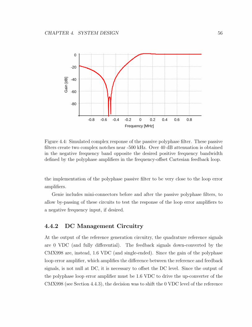
CHAPTER 4. SYSTEM DESIGN 56
Frequency [MHz]-0.8
Gai
n [d
B]
-80
-60
-40
-20
0
-0.6 -0.4 -0.2 0 0.2 0.4 0.6 0.8
Figure 4.4: Simulated complex response of the passive polyphase filter. These passivefilters create two complex notches near -500 kHz. Over 40 dB attenuation is obtainedin the negative frequency band opposite the desired positive frequency bandwidthdefined by the polyphase amplifiers in the frequency-offset Cartesian feedback loop.
the implementation of the polyphase passive filter to be very close to the loop error
amplifiers.
Genie includes mini-connectors before and after the passive polyphase filters, to
allow by-passing of these circuits to test the response of the loop error amplifiers to
a negative frequency input, if desired.
4.4.2 DC Management Circuitry
At the output of the reference generation circuitry, the quadrature reference signals
are 0 VDC (and fully differential). The feedback signals down-converted by the
CMX998 are, instead, 1.6 VDC (and single-ended). Since the gain of the polyphase
loop error amplifier, which amplifies the difference between the reference and feedback
signals, is not null at DC, it is necessary to offset the DC level. Since the output of
the polyphase loop error amplifier must be 1.6 VDC to drive the up-converter of the
CMX998 (see Section 4.4.3), the decision was to shift the 0 VDC level of the reference

CHAPTER 4. SYSTEM DESIGN 57
signals to the latter.
In a classic Cartesian feedback loop, complex DC management strategies would
be necessary for the minimization of the DC offset between all the signal lines at the
input of the loop error amplifiers. Here, the modification implemented with the use
of the polyphase loop error amplifiers relaxes this requirement substantially.
For this reason, to shift the DC level, simple circuitry is sufficient that consists
of a pair of fully differential amplifiers with the common mode control pin receiving
the buffered reference of 1.6 VDC provided by the CMX998; similarly, to compensate
for DC offsets, a simple balanced passive network is sufficient where each quadrature
differential signal line at the input of the polyphase loop error amplifier receives a
manually trimmed constant voltage from a buffer.
4.4.3 Polyphase Amplifier Loop Filter
The polyphase amplifier in Genie has the same fully-differential architecture shown
and discussed in Chapter 3. The simplified schematic is also reproduced here, in
Figure 4.5. The polyphase amplifier was implemented using a pair of fully-differential
amplifiers, model THS4131 by Texas Instruments. The mismatch of the passive com-
ponents, both resistors and capacitors, is 0.1% to guarantee at least 60 dB rejection
to quadrature mismatches created in the feedback path.
The actual values of these components were chosen to obtain a control band with
center frequency ωc of about 500 kHz. The peak gain and passband half-width ωo of
the polyphase amplifiers are about 70 and 140 kHz, respectively.
4.4.4 Mixers and Phase Shift Control
The mixers and phase shift control circuitry of Genie were those of the CMX998
by CML Microcircuits, a commercially available integrated solution for a Cartesian
feedback loop based linear transmitter. This chip also includes an instability detector
and uncommitted op-amps (for input signal conditioning), input amplifiers, filters,
single-ended differential integrators for loop error amplification, and feedback base-
band amplifiers. These circuits were designed for implementing a classic Cartesian
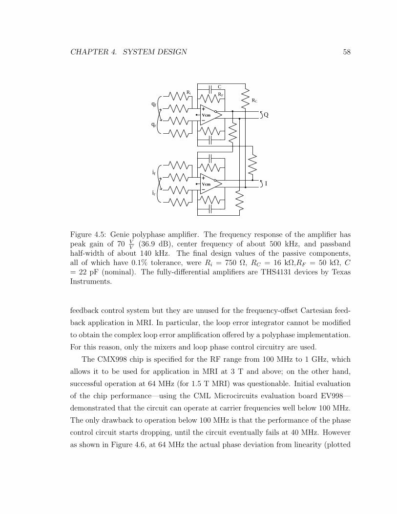
CHAPTER 4. SYSTEM DESIGN 58
Vcm
Vcm
ir
Q
I
if
qr
qf
Ri RF
C
RC
+
−
+
−
Figure 4.5: Genie polyphase amplifier. The frequency response of the amplifier haspeak gain of 70 V
V(36.9 dB), center frequency of about 500 kHz, and passband
half-width of about 140 kHz. The final design values of the passive components,all of which have 0.1% tolerance, were Ri = 750 Ω, RC = 16 kΩ,RF = 50 kΩ, C= 22 pF (nominal). The fully-differential amplifiers are THS4131 devices by TexasInstruments.
feedback control system but they are unused for the frequency-offset Cartesian feed-
back application in MRI. In particular, the loop error integrator cannot be modified
to obtain the complex loop error amplification offered by a polyphase implementation.
For this reason, only the mixers and loop phase control circuitry are used.
The CMX998 chip is specified for the RF range from 100 MHz to 1 GHz, which
allows it to be used for application in MRI at 3 T and above; on the other hand,
successful operation at 64 MHz (for 1.5 T MRI) was questionable. Initial evaluation
of the chip performance—using the CML Microcircuits evaluation board EV998—
demonstrated that the circuit can operate at carrier frequencies well below 100 MHz.
The only drawback to operation below 100 MHz is that the performance of the phase
control circuit starts dropping, until the circuit eventually fails at 40 MHz. However
as shown in Figure 4.6, at 64 MHz the actual phase deviation from linearity (plotted
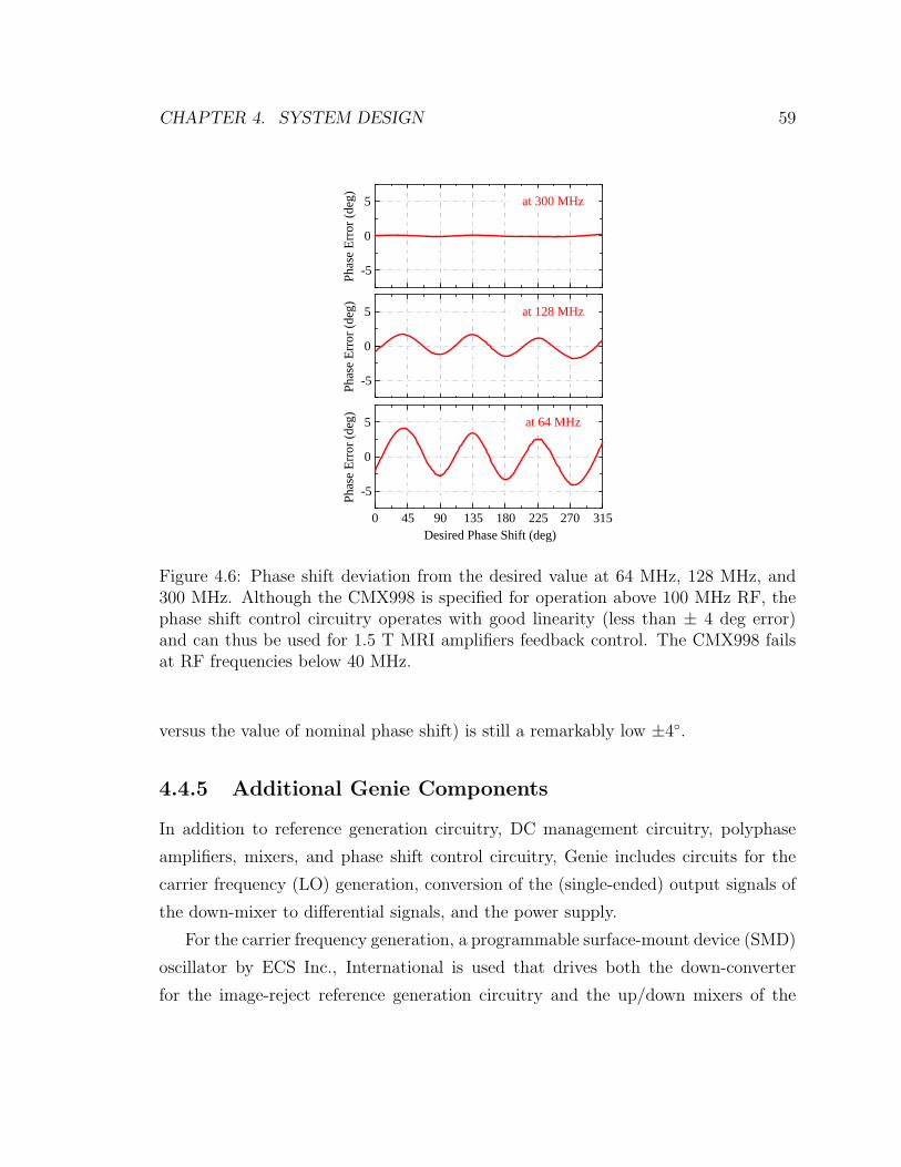
CHAPTER 4. SYSTEM DESIGN 59
0 45 90 135 180 225 270 315
-5
0
5
Desired Phase Shift (deg)
Phas
e Er
ror (
deg)
(63.75+0.25) MHz
-5
0
5
Phas
e Er
ror (
deg)
-5
0
5
Phas
e Er
ror (
deg)
at 64 MHz
at 128 MHz
at 300 MHz
Figure 4.6: Phase shift deviation from the desired value at 64 MHz, 128 MHz, and300 MHz. Although the CMX998 is specified for operation above 100 MHz RF, thephase shift control circuitry operates with good linearity (less than ± 4 deg error)and can thus be used for 1.5 T MRI amplifiers feedback control. The CMX998 failsat RF frequencies below 40 MHz.
versus the value of nominal phase shift) is still a remarkably low ±4.
4.4.5 Additional Genie Components
In addition to reference generation circuitry, DC management circuitry, polyphase
amplifiers, mixers, and phase shift control circuitry, Genie includes circuits for the
carrier frequency (LO) generation, conversion of the (single-ended) output signals of
the down-mixer to differential signals, and the power supply.
For the carrier frequency generation, a programmable surface-mount device (SMD)
oscillator by ECS Inc., International is used that drives both the down-converter
for the image-reject reference generation circuitry and the up/down mixers of the
CHAPTER 4. SYSTEM DESIGN 60
CMX998. This off-the-shelf commercial component can be programmed by the man-
ufacturer or vendor with accuracy of 0.1% (± 6 kHz deviation from the desired 64
MHz frequency, for example). In principle, more accurate devices (such as a direct
digital synthesizer (DDS)) would be desirable to precisely set the center frequency of
the RF control bandwidth; however, in a frequency-offset Cartesian feedback trans-
mitter, variations in the carrier frequency can be compensated for by tuning the
center frequency of the polyphase amplifier passband. (In a classic Cartesian feed-
back transmitter, a more accurate carrier frequency generator would be necessary
since the center frequency of the loop error amplifiers is fixed at DC.) Even more im-
portant, if one wishes to by-pass the reference down-converter of Genie and generate
the low-IF quadrature reference signals using circuitry external to Genie, frequency
errors in the carrier generator would cause phase misalignments between the MRI
reference and the transmitted RF signal. Future generations of Genie should address
this limitation. Here, by using the same LO for the image-reject down-converter and
for the feedback loop, phase errors are cancelled and the output power is phase-locked
to the MRI reference.
To convert the single-ended feedback signals at the output of the CMX998 down-
mixers to differential, a pair of matched unity-gain low-pass amplifiers has been used.
The output signal lines of these amplifiers include 470 nF series capacitors to allow
optional AC-coupling of the feedback signals at the input of the polyphase loop driver
amplifiers.
The bias to all the components on board is obtained by means of four low dropout
(LDO) linear regulators (one LM2990, one LM1086, and two LP2992 devices by
National Instruments) that convert the input +-7 V to +5 V, -5 V, +3.3 V (digital),
and +3.3 V (analog). Genie’s current consumption is 350 mA with zero reference
input signal, and up to 700 mA at maximum control output signal.
4.5 Closing the Loop
At various times during development, the system included different types of loads and
RF power amplifiers. Different coupling devices have also been investigated to sample

CHAPTER 4. SYSTEM DESIGN 61
the output voltage and current of the power amplifier, or, the forward voltage and
reverse voltage of the transmission line between the amplifier and load. RF switches
have also been added to the system to support auto-calibration, that is, for setting of
the stability conditions of the feedback system before each use. Finally, the network
analyzer-like capabilities of a Medusa console developed by Pascal Stang have been
used to provide the reference RF signal, analyze the feedback variable, and gate the
RF switches for auto-calibration.
The above list does not include the components of a load-pull set that has been
used to demonstrate the electronic manipulation of the output impedance of the RF
power amplifier. These components will be described in Chapter 6. Also in this
chapter the use of balanced amplifiers and of vector multipliers in the feedback path
will be presented.
4.5.1 Power Amplifiers
Typical MRI power amplifiers are expensive and low-efficiency class A or A/B RF
amplifiers with output power level ranging from 100 W to even 30 kW. An example of
this class of devices is the A/B wideband power amplifier KAA2040 by AR Modular
RF. At a cost of $10,000, it delivers in excess of 200 W power into a 50 Ω load over
the frequency range of 500 kHz to 100 MHz with nominal power gain of 53 dB. The
KAA2040 has been used in the frequency-offset Cartesian feedback system especially
during the initial stages of development.
The limited output power of Genie combined with the power gain of the KAA2040,
however, is not sufficient to drive the power amplifier up to its full power capabilities.
For this reason, as an alternative to the KAA2040, a set of custom-made 200 W
to 250 W (depending on supply voltage) class A/B power amplifiers with power
gain in excess of 60 dB have been preferred to demonstrate the linearization and
impedance manipulation of the feedback system up to the full output power range.
These amplifiers were built using an AN779H 20 W predriver and an AR313 amplifier
by Communication Concepts, Inc. and corresponding application notes by Motorola,
Inc. [27, 28, 74]. These kits were modified to incorporate RF gating, to perform
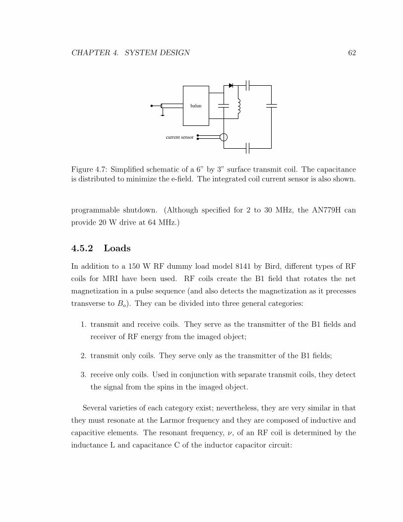
CHAPTER 4. SYSTEM DESIGN 62
Figure 4.7: Simplified schematic of a 6” by 3” surface transmit coil. The capacitanceis distributed to minimize the e-field. The integrated coil current sensor is also shown.
programmable shutdown. (Although specified for 2 to 30 MHz, the AN779H can
provide 20 W drive at 64 MHz.)
4.5.2 Loads
In addition to a 150 W RF dummy load model 8141 by Bird, different types of RF
coils for MRI have been used. RF coils create the B1 field that rotates the net
magnetization in a pulse sequence (and also detects the magnetization as it precesses
transverse to Bo). They can be divided into three general categories:
1. transmit and receive coils. They serve as the transmitter of the B1 fields and
receiver of RF energy from the imaged object;
2. transmit only coils. They serve only as the transmitter of the B1 fields;
3. receive only coils. Used in conjunction with separate transmit coils, they detect
the signal from the spins in the imaged object.
Several varieties of each category exist; nevertheless, they are very similar in that
they must resonate at the Larmor frequency and they are composed of inductive and
capacitive elements. The resonant frequency, ν, of an RF coil is determined by the
inductance L and capacitance C of the inductor capacitor circuit:
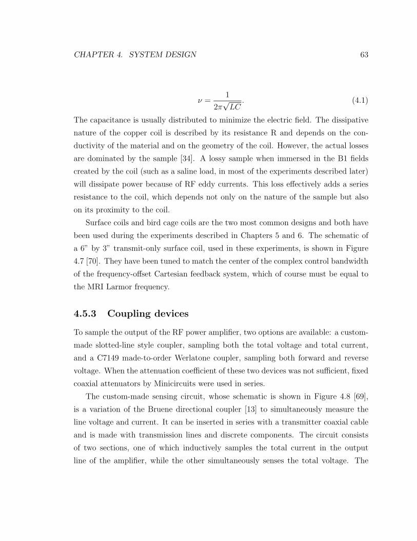
CHAPTER 4. SYSTEM DESIGN 63
ν =1
2π√LC
. (4.1)
The capacitance is usually distributed to minimize the electric field. The dissipative
nature of the copper coil is described by its resistance R and depends on the con-
ductivity of the material and on the geometry of the coil. However, the actual losses
are dominated by the sample [34]. A lossy sample when immersed in the B1 fields
created by the coil (such as a saline load, in most of the experiments described later)
will dissipate power because of RF eddy currents. This loss effectively adds a series
resistance to the coil, which depends not only on the nature of the sample but also
on its proximity to the coil.
Surface coils and bird cage coils are the two most common designs and both have
been used during the experiments described in Chapters 5 and 6. The schematic of
a 6” by 3” transmit-only surface coil, used in these experiments, is shown in Figure
4.7 [70]. They have been tuned to match the center of the complex control bandwidth
of the frequency-offset Cartesian feedback system, which of course must be equal to
the MRI Larmor frequency.
4.5.3 Coupling devices
To sample the output of the RF power amplifier, two options are available: a custom-
made slotted-line style coupler, sampling both the total voltage and total current,
and a C7149 made-to-order Werlatone coupler, sampling both forward and reverse
voltage. When the attenuation coefficient of these two devices was not sufficient, fixed
coaxial attenuators by Minicircuits were used in series.
The custom-made sensing circuit, whose schematic is shown in Figure 4.8 [69],
is a variation of the Bruene directional coupler [13] to simultaneously measure the
line voltage and current. It can be inserted in series with a transmitter coaxial cable
and is made with transmission lines and discrete components. The circuit consists
of two sections, one of which inductively samples the total current in the output
line of the amplifier, while the other simultaneously senses the total voltage. The
CHAPTER 4. SYSTEM DESIGN 64
f (I)
f(V)
1:0.01
1:1
1:11 pF
50 Ω
25 Ω
25 Ω
Figure 4.8: Photo (left) and simplified schematic (right) of custom-made slotted-linestyle sensing circuit. A tapped RC is used for voltage sensing and a pick-up loop forcurrent sensing.
coupling coefficient of both sections is approximately 40 dB at 64 MHz. It is essen-
tially a narrowband device, since its coupling coefficients exhibit an approximately
linear dependence with frequency, increasing approximately by 20 dB per decade of
frequency.
The C7149 coupler by Werlatone is a high-power (200 W), wide bandwidth (60-600
MHz) bidirectional coupler that samples both forward voltage and reverse voltage,
with attenuation coefficient equal to 20±0.5 dB over the entire range.
The relationships between the output voltage, output current, and forward or
reverse transmission line voltages are described by the following equations:
Itot =VFWD − VREV
Z0
(4.2)
Vtot = VFWD + VREV . (4.3)
The s-parameters of the custom-made coupler and of the C7149 coupler are presented
in Table 4.1 and Table 4.2, respectively.
CHAPTER 4. SYSTEM DESIGN 65
Table 4.1: S-parameters of custom-made coupler. Port 1 = Input; Port 2 = Output;Port 3 = Voltage Sample; Port 4 = Current Sample.
InputPort 1 Port 2 Port 3 Port 4
Outp
ut Port 1 0.04406 73.0 0.9940 6 -8.1 0.0104 6 -112.6 0.08906 57.8
Port 2 0.99406 -8.1 0.0447 6 73.1 0.01056 -112.4 0.00886 -122Port 3 0.01046 -112.6 0.01056 -112.4 0.11206 69.1 0.00016 100Port 4 0.08906 57.8 0.00886 -122 0.00016 100 0.28006 58.5
Table 4.2: S-parameters of C7149 coupler by Werlatone. Port 1 = Input; Port 2 =Output; Port 3 = Forward Voltage Sample; Port 4 = Reverse Voltage Sample.
InputPort 1 Port 2 Port 3 Port 4
Outp
ut Port 1 0.02606 -33.0 0.99006 -29.3 0.09566 -16.2 0.00146 60.0
Port 2 0.99006 -29.3 0.02706 -30.0 0.00266 16.0 0.09626 15.0Port 3 0.09566 -16.2 0.0026 6 16.0 0.02166 -143 0.97306 -151.7Port 4 0.0014 6 60.0 0.0962 6 15.0 0.97306 -151.7 0.01736 -138.0
Combiners
Commercially available, 2-way power combiners by Mini-circuits are used to com-
bine the outputs of the couplers (or, of the vector multipliers) to obtain the desired
feedback signal at the input of Genie’s down-converter. Both 0 combiners (model
ZFSC-2-4+) and 180 combiners (model ZFSCJ-2-4+) are available, to perform sum
and subtraction, respectively, of two samples.
4.5.4 Auto-Calibration Network
An automated switching network has been developed for the calibration of the feed-
back system in which RF switches toggle the system from the open-loop to the closed-
loop configuration. At the beginning of each experiment, the system is in open-loop
configuration and the phase shift setting that ensures the stability of the closed system
is measured and implemented by controlling the phase shift circuitry of the CMX998
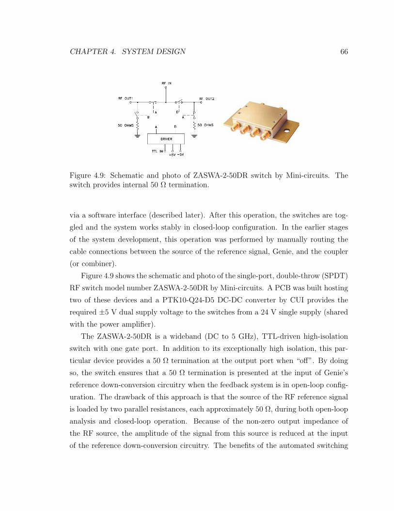
CHAPTER 4. SYSTEM DESIGN 66
Figure 4.9: Schematic and photo of ZASWA-2-50DR switch by Mini-circuits. Theswitch provides internal 50 Ω termination.
via a software interface (described later). After this operation, the switches are tog-
gled and the system works stably in closed-loop configuration. In the earlier stages
of the system development, this operation was performed by manually routing the
cable connections between the source of the reference signal, Genie, and the coupler
(or combiner).
Figure 4.9 shows the schematic and photo of the single-port, double-throw (SPDT)
RF switch model number ZASWA-2-50DR by Mini-circuits. A PCB was built hosting
two of these devices and a PTK10-Q24-D5 DC-DC converter by CUI provides the
required ±5 V dual supply voltage to the switches from a 24 V single supply (shared
with the power amplifier).
The ZASWA-2-50DR is a wideband (DC to 5 GHz), TTL-driven high-isolation
switch with one gate port. In addition to its exceptionally high isolation, this par-
ticular device provides a 50 Ω termination at the output port when “off”. By doing
so, the switch ensures that a 50 Ω termination is presented at the input of Genie’s
reference down-conversion circuitry when the feedback system is in open-loop config-
uration. The drawback of this approach is that the source of the RF reference signal
is loaded by two parallel resistances, each approximately 50 Ω, during both open-loop
analysis and closed-loop operation. Because of the non-zero output impedance of
the RF source, the amplitude of the signal from this source is reduced at the input
of the reference down-conversion circuitry. The benefits of the automated switching
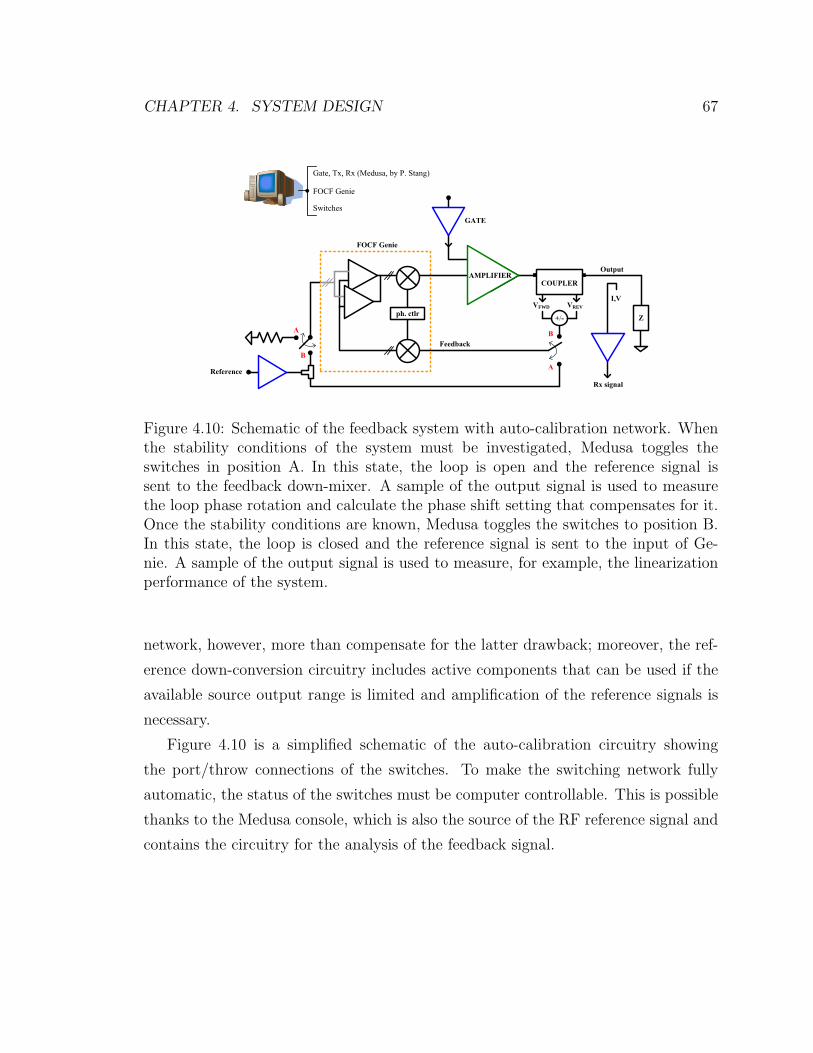
CHAPTER 4. SYSTEM DESIGN 67
FWD REV
Figure 4.10: Schematic of the feedback system with auto-calibration network. Whenthe stability conditions of the system must be investigated, Medusa toggles theswitches in position A. In this state, the loop is open and the reference signal issent to the feedback down-mixer. A sample of the output signal is used to measurethe loop phase rotation and calculate the phase shift setting that compensates for it.Once the stability conditions are known, Medusa toggles the switches to position B.In this state, the loop is closed and the reference signal is sent to the input of Ge-nie. A sample of the output signal is used to measure, for example, the linearizationperformance of the system.
network, however, more than compensate for the latter drawback; moreover, the ref-
erence down-conversion circuitry includes active components that can be used if the
available source output range is limited and amplification of the reference signals is
necessary.
Figure 4.10 is a simplified schematic of the auto-calibration circuitry showing
the port/throw connections of the switches. To make the switching network fully
automatic, the status of the switches must be computer controllable. This is possible
thanks to the Medusa console, which is also the source of the RF reference signal and
contains the circuitry for the analysis of the feedback signal.
CHAPTER 4. SYSTEM DESIGN 68
4.5.5 Medusa
Medusa was developed by Pascal Stang at MRSRL for parallel imaging applications,
as well as for vector modulation of an array system for parallel transmit and array
coil decoupling [73]. It is built from an extensible set of intelligent RF and gradient
modules, including local synchronization logic, a Direct Memory Access (DMA) en-
gine, and a 2-megabyte waveform buffer, which together provide the core functionality
required by MRI.
Medusa’s network analyzer-like capabilities supported the system development
described in this chapter by providing an RF reference signal to Genie, receiving and
analyzing a copy of the feedback signal sent to the CMX998 down-mixer, gating the
power amplifier synchronously with the onset and duration of the reference signal (in
order to avoid excessive dissipation and thus heating, which could irreversibly damage
its functionality), and controlling the RF switches to toggle the system configuration
between open- and closed-loop.
Medusa can be controlled entirely via PC, using a Matlab interface. In addition
to the routines necessary for the automatic calibration of the loop, several pulse se-
quence routines were developed to investigate the performance of the frequency-offset
Cartesian feedback system in a variety of experiments. Some routines, for example,
allow the generation of the reference signals and the measurement of the linearization
performance of the system at varying signal amplitudes (at fixed frequency) or fre-
quencies (at fixed amplitude). Other routines create MRI-like modulated reference
signals such as sinc pulses, Gaussian pulses, rectangular pulses, or more complicated
Very Selective Saturation pulses [77]. Other routines control the auxiliary circuitry
necessary for measuring the output impedance of the power amplifier (the load pull
setup, see Chapter 6) or for changing phase and amplitude of the sampled forward
and reverse voltages from the Werlatone coupler with the vector multipliers. Higher-
level routines combine these capabilities to analyze the performance of the system
when multiple functionalities are needed at once.
In addition to controlling Medusa, it is also possible to control the CMX998 mixers’
gain and phase shift settings via PC. To do so, two options have been demonstrated.
One consists of using the commercially available PE001 card and GUI interface by
CHAPTER 4. SYSTEM DESIGN 69
CML Microcircuits. The other is based on a development board hosting an AVR
processor by Atmel controlled via a Matlab interface.
4.5.6 PE001 Card and GUI Interface
The PE0001 interface card is a global interface system designed for use with evaluation
kits for new generation ICs manufactured by CML. Supplied with a PC GUI, the
PE0001 provides a graphical method of addressing all the CMX998 on-chip registers
via the C-BUS interface. The information generated by the GUI is formatted, timed
and delivered to the target IC via the C-BUS serial interface hosted by Genie. Power
to the PE0001 is also obtained from Genie via the same serial connector.
The PE0001 card and GUI interface offer many capabilities; however, given that
only the mixers and phase shift circuitry of the CMX998 are used, the card and
interface are used only to address the registers that enable the CMX998 bias, enable
the forward and feedback circuitry, select the gain of the mixers (to modify the forward
and feedback loop gain), and control the phase shift circuitry.
4.5.7 AVRmini and Matlab Interface
As an alternative to the PE0001 card, the use of an AVRmini V4.0 development board
(by P. Stang) with Ethernet and USB, hosting an ATmega644P AVR processor by
Atmel, has also been demonstrated. The board is connected to Genie via a second
serial connector, and to a PC via Ethernet. The AVRmini is programmed by Matlab
and fully replaces all functions supported by the PE0001, that is, it enables the
CMX998 bias, forward and feedback circuitry, selects the gain of the mixers, and
controls the phase shift circuitry. It does so with the added advantage that the number
of conductive pathways between Genie and the PC is reduced to that necessary for
the Medusa console only. One drawback of this option is that, without the PE0001
GUI interface, the values stored in the CMX998 registers are not all immediately
visible at any time, which makes testing more cumbersome.
This section concludes the description of the components in the frequency-offset
Cartesian feedback system. In the next section, a theoretical analysis of the loop
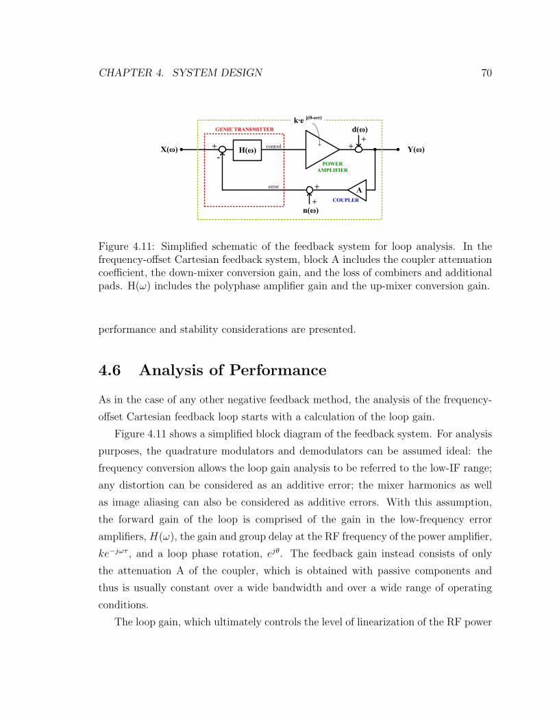
CHAPTER 4. SYSTEM DESIGN 70
+ control
error
GENIE TRANSMITTER
COUPLER
-H(ω)
POWER AMPLIFIER
k·e j(θ-ωτ)
A
Z
X(ω) Y(ω)+
d(ω)
+
n(ω)
+
+
Figure 4.11: Simplified schematic of the feedback system for loop analysis. In thefrequency-offset Cartesian feedback system, block A includes the coupler attenuationcoefficient, the down-mixer conversion gain, and the loss of combiners and additionalpads. H(ω) includes the polyphase amplifier gain and the up-mixer conversion gain.
performance and stability considerations are presented.
4.6 Analysis of Performance
As in the case of any other negative feedback method, the analysis of the frequency-
offset Cartesian feedback loop starts with a calculation of the loop gain.
Figure 4.11 shows a simplified block diagram of the feedback system. For analysis
purposes, the quadrature modulators and demodulators can be assumed ideal: the
frequency conversion allows the loop gain analysis to be referred to the low-IF range;
any distortion can be considered as an additive error; the mixer harmonics as well
as image aliasing can also be considered as additive errors. With this assumption,
the forward gain of the loop is comprised of the gain in the low-frequency error
amplifiers, H(ω), the gain and group delay at the RF frequency of the power amplifier,
ke−jωτ , and a loop phase rotation, ejθ. The feedback gain instead consists of only
the attenuation A of the coupler, which is obtained with passive components and
thus is usually constant over a wide bandwidth and over a wide range of operating
conditions.
The loop gain, which ultimately controls the level of linearization of the RF power

CHAPTER 4. SYSTEM DESIGN 71
amplifier, is thus
G(ω) = Ak|H(ω)|ejθ−jωτ+j 6 H(ω) (4.4)
and the output control variable is
Y (ω) = X(ω)k|H(ω)|ejθ−jωτ+j 6 H(ω)
1 + Ak|H(ω)|ejθ−jωτ+6 H(ω). (4.5)
If the conditions for stability are met, and Ak|H(ω)| is greater than unity within the
control bandwidth, then
Y (ω) ≈ X(ω)1
A(4.6)
that is, the gain of the system is determined by the attenuation of the coupler only
and the output signal is free, to first order approximation, from the distortion of the
power amplifier.
To understand the effect of the loop on noise and distortion created by the blocks
of the system, two summing junctions can be included in the forward path and in
the feedback path, respectively, into which distortion and noise (d(ω) and n(ω)) are
added. In this case,
Y (ω) = X(ω)k|H(ω)|ejθ−jωτ+j 6 H(ω)
1 + Ak|H(ω)|ejθ−jωτ+6 H(ω)
+d(ω)1
1 + Ak|H(ω)|ejθ−jωτ+6 H(ω)
+n(ω)Ak|H(ω)|ejθ−jωτ+j 6 H(ω)
1 + Ak|H(ω)|ejθ−jωτ+ 6 H(ω).
(4.7)
Assuming, for the moment, that the loop is stable and Ak|H(ω)| is greater than unity,
then
Y (ω) ≈ X(ω)1
A+ d(ω)
1
G(ω)+ n(ω). (4.8)
The noise and distortion d(ω) produced by the blocks in the forward path are reduced
by a factor equal to the loop gain by the inclusion of the feedback loop. Thus, for
example, if the loop gain is 10, the distortion of the closed loop system will be 20

CHAPTER 4. SYSTEM DESIGN 72
dB lower than the distortion introduced by the blocks in the forward path, which is
usually dominated by the power amplifier.
The noise and distortion n(ω) produced by the blocks in the feedback path, in-
stead, directly corrupt the output of the closed system. For this reason, minimizing
any source of noise and distortion in the feedback path is extremely important.
4.7 Analysis of Stability
For the closed loop transmission to be determined (mostly) by the coupler coefficient
only, the conditions for stability of the loop must be met. As in the classic Cartesian
feedback system, the conditions for stability are as follows:
1. the phase adjuster must be set to cancel any phase shift (phase rotation) around
the loop (i.e., force θ equal to 0);
2. the loop phase margin pm should be at least 45.
The phase margin (pm) is the difference between the phase of G(ω) and 180 (or
-180) when the loop gain is unity (i.e., ω = ωpm, the unity gain crossover frequency):
pm = π − (θ − ωpmτ + 6 H(ωpm)). (4.9)
When the loop gain approaches unity, the ability of the loop to reduce the distortion
of the power amplifier is effectively nil. In a frequency-offset Cartesian feedback
system, the separation between ωpm and ωc (the center frequency of the polyphase
complex band) is thus the minimum desired half-width of the control bandwidth.
In other words, ωpm must be at least larger than half the modulation bandwidth
of the desired signal, and should include the intermodulation bandwidth (since only
intermodulation products within the control bandwidth can be linearized). With this
requirement on ωpm and assuming that the phase rotation is compensated for, then
the specification on the minimum phase margin drives the design of H(ωpm), that
is, it dictates the choice of peak gain and pole frequency of the polyphase loop error
amplifiers described in Chapter 3.
CHAPTER 4. SYSTEM DESIGN 73
If the phase rotation is not compensated, the phase margin can become less than
45 and stability can be compromised. For example, positive phase error increases
the phase margin for positive offset frequencies and reduces it for negative offset
frequencies. When the phase error is negative, the opposite happens.
The loop gain of the frequency-offset Cartesian feedback loop has changed sig-
nificantly during the design, since different power amplifiers and couplers have been
used. In general, the system was characterized by loop gain of magnitude in the range
10 to 20 and with a stable control band 50 kHz to 100 kHz wide.
The contributions (and limitations) to the loop gain of the frequency-offset Carte-
sian feedback system are shown in Table 4.3. In particular, gain and dynamic range
of all the main components in Genie, including not only the polyphase amplifiers but
also the variable gain amplifiers following the mixers in the forward and feedback
path, dictated the choice of having an overall feedback attenuation (including the
attenuation coefficient A and down-mixer gain) usually equal or slightly higher (by
10 dB to 14 dB) than the amplification k of the RF power amplifier. The magnitude
of the loop gain is thus, generally, equal to or lower (by the same amount) than the
peak gain of the polyphase amplifiers (including the up-mixer gain, always kept at its
highest value of -2dB). With a polyphase gain of about 70, the loop gain magnitude
ranged between 10 (17 dB below 70) and 20 (11 dB below 70).
While traditional frequency response techniques can be applied to a single Carte-
sian feedback control loop and offer a useful starting point for further stability anal-
ysis, the situation where multiple loops control different resonant loads inductively-
coupled to one another is of particular interest in MRI and the possibility to study the
stability of the latter with traditional methods of analysis is debated. The application
of the control theory for Multiple-Input, Multiple-Output (MIMO) systems might be
a solution to this problem. However, this approach to the study of stability can be
extremely challenging. Simpler approaches would be desirable. The application of
the Middlebrook criterion [56–58] to arrays of control loops could be a solution to
this problem. While the application of this method has not been verified in practice,
it might represent a starting point for the understanding of the effects of coil-to-coil
interactions on stability. One of the most interesting results of this analysis is that
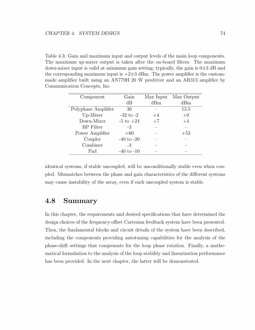
CHAPTER 4. SYSTEM DESIGN 74
Table 4.3: Gain and maximum input and output levels of the main loop components.The maximum up-mixer output is taken after the on-board filters. The maximumdown-mixer input is valid at minimum gain setting; typically, the gain is 0±3 dB andthe corresponding maximum input is +2∓3 dBm. The power amplifier is the custom-made amplifier built using an AN779H 20 W predriver and an AR313 amplifier byCommunication Concepts, Inc.
Component Gain Max Input Max OutputdB dBm dBm
Polyphase Amplifier 36 – 13.5Up-Mixer -32 to -2 +4 +0
Down-Mixer -5 to +24 +7 +4BP Filter -3 – –
Power Amplifier +60 – +53Coupler -40 to -20 – –
Combiner -3 – –Pad -40 to -10 – –
identical systems, if stable uncoupled, will be unconditionally stable even when cou-
pled. Mismatches between the phase and gain characteristics of the different systems
may cause instability of the array, even if each uncoupled system is stable.
4.8 Summary
In this chapter, the requirements and desired specifications that have determined the
design choices of the frequency-offset Cartesian feedback system have been presented.
Then, the fundamental blocks and circuit details of the system have been described,
including the components providing autotuning capabilities for the analysis of the
phase-shift settings that compensate for the loop phase rotation. Finally, a mathe-
matical formulation to the analysis of the loop stability and linearization performance
has been provided. In the next chapter, the latter will be demonstrated.
Chapter 5
Improving the Fidelity of RF
Reproduction
5.1 Introduction
As the frequency and bandwidth of the MRI signal increase, the problem of the
RF distortion in the transmit path becomes non-negligible. The frequency-offset
Cartesian feedback method and system employing power amplifiers for MRI promises
to address this problem by providing increased fidelity of RF reproduction.
In this chapter, the nature of the distortion created by the behavior of any RF
power amplifier is briefly discussed. Then, the ability of the feedback system to
improve the fidelity of RF reproduction is demonstrated in a number of situations:
not only have different types of tests been performed, but also different variables—
such as the output voltage of the power amplifier, or the output current, or even the
transmit coil current—have been chosen as the feedback control loop variable.
The conventional linearity tests used in the field of communications to demonstrate
the performance of a classic Cartesian feedback system have also been performed and
are described here. These tests show that the frequency-offset Cartesian feedback
system offers state of the art performance equal to the classic implementation. In
addition, experiments have been conducted to show that excellent performance is
obtained with much relaxed specifications for the transmitter, thanks to the use
75
CHAPTER 5. IMPROVING THE FIDELITY OF RF REPRODUCTION 76
of polyphase loop error amplifiers. Indeed, if the polyphase loop error amplifiers
are modified to obtain the classic loop error amplifiers, the system performance is
significantly hindered.
To demonstrate the significance of the application of the frequency-offset Carte-
sian feedback system in MRI, the effects of using the system have been demonstrated
with a variety of typical MRI pulses, such as sinc pulses, Gaussian pulses, rectangu-
lar pulses, and many more. Some of the results obtained in these experiments are
described here.
Finally, the ability to reject the mirror frequency of the desired reference signal
at the carrier has been measured. This test shows that the system is capable of a
significant rejection of the undesired frequencies created by the down-mixer.
5.2 Nature of Amplifier Distortion
Amplifier distortion has been a concern for many years in virtually every field of ampli-
fier design. The nature of such distortion is usually described in terms of amplitude-
to-amplitude (AM-AM) distortion, amplitude-to-phase (AM-PM) distortion, phase
dispersion, and memory effects [40].
A perfect amplifier would have a linear transfer characteristic, where the output
signal Sout would be a scalar multiple of the input signal Sin, that is,
Sout(t) = kSin(t) (5.1)
where k is the gain of the amplifier and
Sin = A(t) cos(ωCt). (5.2)
In reality, all practical amplifiers are characterized by a certain degree of amplitude
non-linearity, that is, a relationship between input and output that is a non-linear
function fAM() of the amplitude modulation of the input signal:
Sout(t) = kfAM(A(t)) cos(ωCt). (5.3)
CHAPTER 5. IMPROVING THE FIDELITY OF RF REPRODUCTION 77
This non-linear relationship is often termed AM-AM conversion since it is a conversion
between the amplitude modulation present on the input signal and the distorted
amplitude modulation present on the output signal.
Another effect is a conversion from amplitude modulation of the input signal to
phase modulation on the output signal, and is known as AM-PM conversion. In this
case,
Sout(t) = kA(t) cos(ωCt+ fPM(A(t))) (5.4)
that is, the resulting output spectrum is that of a carrier whose phase is modulated by
a non-linear function fPM() of the amplitude modulation of the input signal. Usually,
the undesired AM-PM modulation at the output of the amplifier is similar to that
resulting from AM-AM non-linearity; since the two forms of distortion often coexist,
separating their effects is generally very difficult.
To complicate the picture even further, a practical amplifier does not delay all
frequency components within the input signal by the same amount when they reach
the output (regardless of the amplitude of each of these components). The relationship
between time delay, τ , and phase shift, ϕ (in radians), is
τ =ϕ
2πf(5.5)
where f is the frequency dispersion. If the time delay is not identical for all frequency
components of the input signal, the phase shift does not increase in proportion to
the frequency and the output waveshape will be distorted. This non-linear phase
characteristic is known as the phase dispersion of the amplifier.
Finally, in all practical amplifiers, the AM/AM, AM/PM and phase dispersion are
not immutable but vary with changes in the environment and with the operating fre-
quency of the amplifier. Typical changes that influence the power amplifier behavior
are fluctuations in the biasing conditions and temperature. The distortions created
by these changes generally fall under the category of memory effects.
In the field of communication the distortion of a power amplifier is usually charac-
terized through standardized tests such as 1 dB compression testing, two-tone testing,
CHAPTER 5. IMPROVING THE FIDELITY OF RF REPRODUCTION 78
and QAM constellation testing. In the field of MRI, while these non-linearity mea-
sures are still very useful, it is easier to appreciate the extent to which the amplifier
distortion affects the quality of an image by solving the Bloch equations and com-
paring the effects on the spin magnetization of a desired (reference input) waveshape
and the experimental (output) MR pulse, distorted by the amplifier.
In the remaining sections of this chapter, simple tests are presented that show the
AM-AM, AM-PM, and phase linearization enhancement obtained with the frequency-
offset Cartesian system over stand-alone MRI power amplifiers. Then, both standard-
ized communication-style test results and MRI-like test results are presented to show
the positive effects of this enhancement on the fidelity of reproduction of the signals
used in both fields.
5.3 Reduced AM-AM, AM-PM Distortion
In a first set of experiments, the AM-AM and AM-PM distortion of the power ampli-
fier is studied and compared with the distortion of the closed-loop feedback system.
To study AM-AM and AM-PM distortion and feedback linearization, a series
of pulses was used as the input reference signal, each pulse consisting of a sinusoidal
signal of fixed frequency and fixed amplitude; all the pulses in the series had the same
duration and frequency, but their amplitude increased in the series. The duration of
the pulse was made much longer than the settling time of the power amplifier (with
or without control feedback loop), so that the distortion could be evaluated when
the amplifier was at equilibrium. Initially, the reference signal was applied directly
at the input of the power amplifier; then, it was applied at the input of the reference
down-converter of the transmitter in the complete feedback system.
Enhanced linearization can be demonstrated in the voltage-to-voltage character-
istic of the power amplifier or in the voltage-to-current characteristic by choosing the
output voltage or output current, respectively, of the amplifier as the feedback vari-
able of the control system. For application in MRI, both situations are of interest,
depending on the particular design of the coil loading the amplifier.
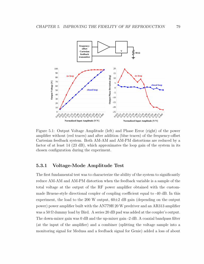
CHAPTER 5. IMPROVING THE FIDELITY OF RF REPRODUCTION 79
0
10
20
30
40
50
60
70
80
90
100
0.0250.0
520.0
790.1
050.1
320.1
590.1
860.2
120.2
390.2
660.2
930.3
200.3
460.3
730.4
00
Normalized Input Amplitude [V/V]
Out
put V
olta
ge [V
]
-25
-20
-15
-10
-5
0
5
10
15
20
0.0250.0
520.0
790.1
050.1
320.1
590.1
860.2
120.2
390.2
660.2
930.3
200.3
460.3
730.4
00
Normalized Input Amplitude [V/V]
Out
put P
hase
Dev
iatio
n [d
eg]
closed loop
no loop
closed loop
no loop
frequency-offset
Cartesian feedback
transmitter
V50 Ω
Figure 5.1: Output Voltage Amplitude (left) and Phase Error (right) of the poweramplifier without (red traces) and after addition (blue traces) of the frequency-offsetCartesian feedback system. Both AM-AM and AM-PM distortions are reduced by afactor of at least 14 (23 dB), which approximates the loop gain of the system in itschosen configuration during the experiment.
5.3.1 Voltage-Mode Amplitude Test
The first fundamental test was to characterize the ability of the system to significantly
reduce AM-AM and AM-PM distortion when the feedback variable is a sample of the
total voltage at the output of the RF power amplifier obtained with the custom-
made Bruene-style directional coupler of coupling coefficient equal to -40 dB. In this
experiment, the load to the 200 W output, 60±2 dB gain (depending on the output
power) power amplifier built with the AN779H 20 W predriver and an AR313 amplifier
was a 50 Ω dummy load by Bird. A series 20 dB pad was added at the coupler’s output.
The down-mixer gain was 0 dB and the up-mixer gain -2 dB. A coaxial bandpass filter
(at the input of the amplifier) and a combiner (splitting the voltage sample into a
monitoring signal for Medusa and a feedback signal for Genie) added a loss of about
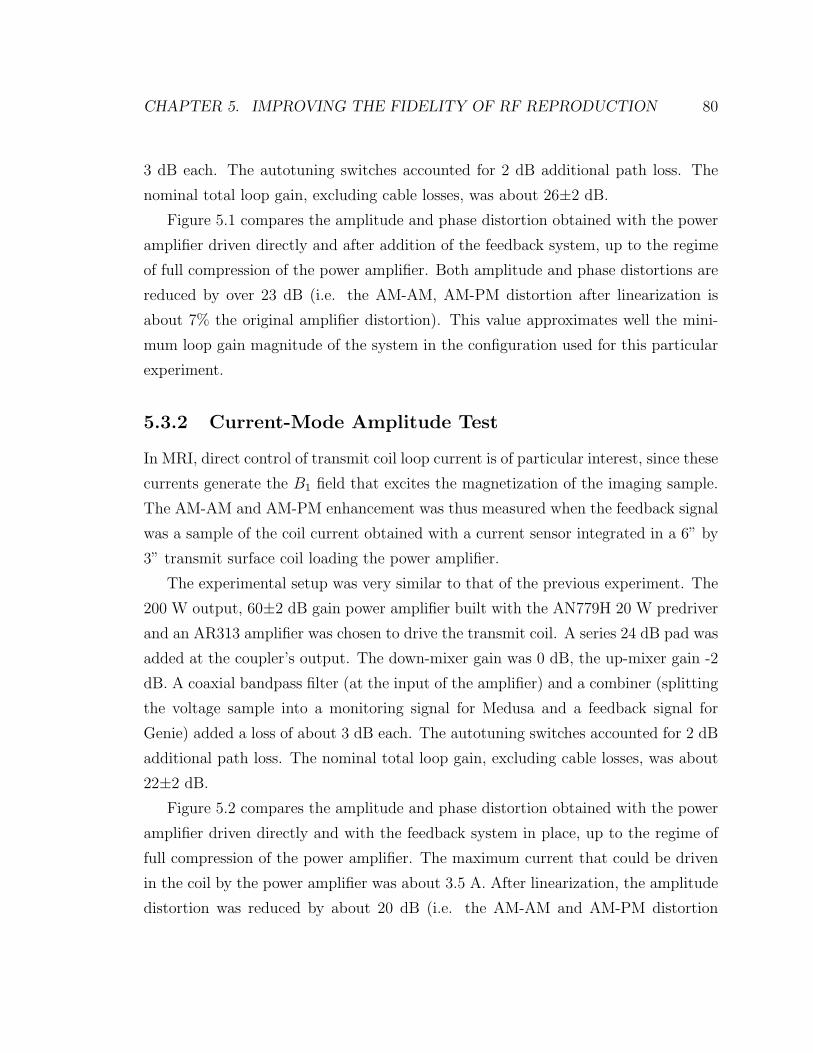
CHAPTER 5. IMPROVING THE FIDELITY OF RF REPRODUCTION 80
3 dB each. The autotuning switches accounted for 2 dB additional path loss. The
nominal total loop gain, excluding cable losses, was about 26±2 dB.
Figure 5.1 compares the amplitude and phase distortion obtained with the power
amplifier driven directly and after addition of the feedback system, up to the regime
of full compression of the power amplifier. Both amplitude and phase distortions are
reduced by over 23 dB (i.e. the AM-AM, AM-PM distortion after linearization is
about 7% the original amplifier distortion). This value approximates well the mini-
mum loop gain magnitude of the system in the configuration used for this particular
experiment.
5.3.2 Current-Mode Amplitude Test
In MRI, direct control of transmit coil loop current is of particular interest, since these
currents generate the B1 field that excites the magnetization of the imaging sample.
The AM-AM and AM-PM enhancement was thus measured when the feedback signal
was a sample of the coil current obtained with a current sensor integrated in a 6” by
3” transmit surface coil loading the power amplifier.
The experimental setup was very similar to that of the previous experiment. The
200 W output, 60±2 dB gain power amplifier built with the AN779H 20 W predriver
and an AR313 amplifier was chosen to drive the transmit coil. A series 24 dB pad was
added at the coupler’s output. The down-mixer gain was 0 dB, the up-mixer gain -2
dB. A coaxial bandpass filter (at the input of the amplifier) and a combiner (splitting
the voltage sample into a monitoring signal for Medusa and a feedback signal for
Genie) added a loss of about 3 dB each. The autotuning switches accounted for 2 dB
additional path loss. The nominal total loop gain, excluding cable losses, was about
22±2 dB.
Figure 5.2 compares the amplitude and phase distortion obtained with the power
amplifier driven directly and with the feedback system in place, up to the regime of
full compression of the power amplifier. The maximum current that could be driven
in the coil by the power amplifier was about 3.5 A. After linearization, the amplitude
distortion was reduced by about 20 dB (i.e. the AM-AM and AM-PM distortion
CHAPTER 5. IMPROVING THE FIDELITY OF RF REPRODUCTION 81
0.0250.0
520.0
790.1
050.1
320.1
590.1
860.2
120.2
390.2
660.2
930.3
200.3
460.3
730.4
00
Normalized Input Amplitude [V/V]
Coi
l Cur
rent
Pha
se D
evia
tion
[I]
-15
-10
-5
0
5
10
15
0
0.5
1
1.5
2
2.5
3
3.5
4
0.0250.0
520.0
790.1
050.1
320.1
590.1
860.2
120.2
390.2
660.2
930.3
200.3
460.3
730.4
00
Normalized Input Amplitude [V/V]
Coi
l Cur
rent
[I]
closed loop
no loop
closed loop
no loop
frequency-offset
Cartesian feedback
transmitter
Figure 5.2: Coil Current Amplitude (left) and Phase Error (right) before and afteraddition of the frequency-offset Cartesian feedback system (shown in red and blue,respectively). Both AM-AM and AM-PM distortions are reduced by a factor of about10 (20 dB) in the range between 10% and 90% of the total output current. This valueapproximates the minimum loop gain of the system in its chosen configuration duringthe experiment. The reduced linearization performance at the extremes of the rangecan be explained by the reduced phase margin, due to the variation in the loadimpedance with varying frequency.
after linearization was about 10% of the original amplifier distortion). Also the phase
distortion was reduced by the same amount, but only within 20% and 90% of the
output range: the plot of phase distortion shows a reduced linearization performance
near the minimum and maximum limits of the power amplifier operating range.
The latter observation, which was not made in the previous experiment, can be
explained by the different type of loading to the power amplifier: in the previous
experiment, the broadband 50 Ω dummy load was presenting a constant impedance
to the amplifier; in this experiment, the transmit coil is a tuned (narrowband) device.
The narrowband behavior of the coil affects the phase margin of the feedback system,
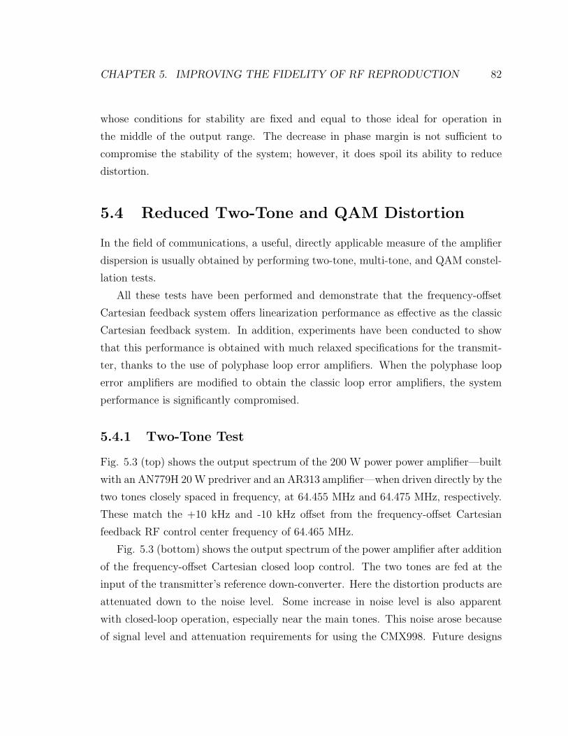
CHAPTER 5. IMPROVING THE FIDELITY OF RF REPRODUCTION 82
whose conditions for stability are fixed and equal to those ideal for operation in
the middle of the output range. The decrease in phase margin is not sufficient to
compromise the stability of the system; however, it does spoil its ability to reduce
distortion.
5.4 Reduced Two-Tone and QAM Distortion
In the field of communications, a useful, directly applicable measure of the amplifier
dispersion is usually obtained by performing two-tone, multi-tone, and QAM constel-
lation tests.
All these tests have been performed and demonstrate that the frequency-offset
Cartesian feedback system offers linearization performance as effective as the classic
Cartesian feedback system. In addition, experiments have been conducted to show
that this performance is obtained with much relaxed specifications for the transmit-
ter, thanks to the use of polyphase loop error amplifiers. When the polyphase loop
error amplifiers are modified to obtain the classic loop error amplifiers, the system
performance is significantly compromised.
5.4.1 Two-Tone Test
Fig. 5.3 (top) shows the output spectrum of the 200 W power power amplifier—built
with an AN779H 20 W predriver and an AR313 amplifier—when driven directly by the
two tones closely spaced in frequency, at 64.455 MHz and 64.475 MHz, respectively.
These match the +10 kHz and -10 kHz offset from the frequency-offset Cartesian
feedback RF control center frequency of 64.465 MHz.
Fig. 5.3 (bottom) shows the output spectrum of the power amplifier after addition
of the frequency-offset Cartesian closed loop control. The two tones are fed at the
input of the transmitter’s reference down-converter. Here the distortion products are
attenuated down to the noise level. Some increase in noise level is also apparent
with closed-loop operation, especially near the main tones. This noise arose because
of signal level and attenuation requirements for using the CMX998. Future designs
CHAPTER 5. IMPROVING THE FIDELITY OF RF REPRODUCTION 83
Figure 5.3: Two-tone Test. The output spectrum of the power amplifier drivendirectly (top) with two tones closely spaced in frequency shows odd-order inter-modulation products, which are reduced to the noise floor after addition of thefrequency-offset Cartesian feedback system (bottom). Some increase in noise levelis evident with closed-loop operation, especially near the main tones.
of the system transmitter can address this limitation, and optimization strategies
are available since the noise analysis of a frequency-offset Cartesian feedback system
should be equivalent to the noise analysis of a classic Cartesian feedback loop.
The two-tone distortion results are repeated in Figure 5.4 for the classic Cartesian
feedback configuration, obtained by removing the crossing resistors of the polyphase
loop error amplifiers (and thus, the coupling between I/Q error signals) to obtain a
pair of classic low-pass amplifiers. Figure 5.4(top) shows the output spectrum of the
power amplifier when directly driven by two tones at 64.01 MHz and 63.99 MHz (these
tones are +10 kHz and -10 kHz offset from the LO and control center frequency of 64
MHz). Figure 5.4(bottom) shows the output spectrum of the power amplifier when
controlled by the classic transmitter configuration. The system reduces the distortion
products down to the noise level, just as the frequency-offset Cartesian feedback
system does, but some LO-leakage and LO-noise is evident. More precise trimming of
DC-offsets would have suppressed this effect. The frequency-offset Cartesian feedback
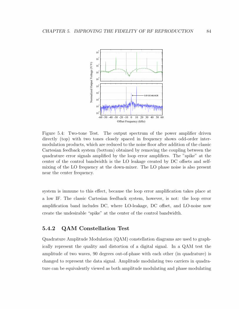
CHAPTER 5. IMPROVING THE FIDELITY OF RF REPRODUCTION 84
Figure 5.4: Two-tone Test. The output spectrum of the power amplifier drivendirectly (top) with two tones closely spaced in frequency shows odd-order inter-modulation products, which are reduced to the noise floor after addition of the classicCartesian feedback system (bottom) obtained by removing the coupling between thequadrature error signals amplified by the loop error amplifiers. The ”spike” at thecenter of the control bandwidth is the LO leakage created by DC offsets and self-mixing of the LO frequency at the down-mixer. The LO phase noise is also presentnear the center frequency.
system is immune to this effect, because the loop error amplification takes place at
a low IF. The classic Cartesian feedback system, however, is not: the loop error
amplification band includes DC, where LO-leakage, DC offset, and LO-noise now
create the undesirable “spike” at the center of the control bandwidth.
5.4.2 QAM Constellation Test
Quadrature Amplitude Modulation (QAM) constellation diagrams are used to graph-
ically represent the quality and distortion of a digital signal. In a QAM test the
amplitude of two waves, 90 degrees out-of-phase with each other (in quadrature) is
changed to represent the data signal. Amplitude modulating two carriers in quadra-
ture can be equivalently viewed as both amplitude modulating and phase modulating
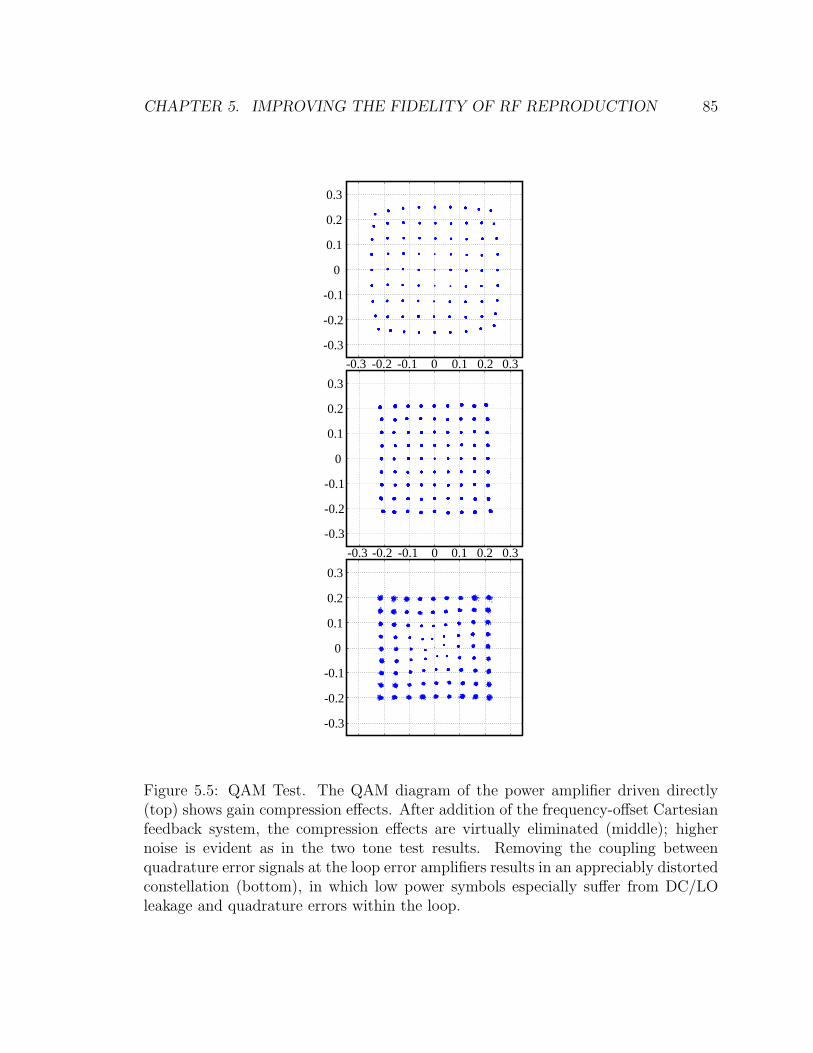
CHAPTER 5. IMPROVING THE FIDELITY OF RF REPRODUCTION 85
-0.3
-0.2
-0.1
0
0.1
0.2
0.3
-0.3 -0.2 -0.1 0 0.1 0.2 0.3-0.3
-0.2
-0.1
0
0.1
0.2
0.3
-0.3
-0.2
-0.1
0
0.1
0.2
0.3
-0.3 -0.2 -0.1 0 0.1 0.2 0.3
Figure 5.5: QAM Test. The QAM diagram of the power amplifier driven directly(top) shows gain compression effects. After addition of the frequency-offset Cartesianfeedback system, the compression effects are virtually eliminated (middle); highernoise is evident as in the two tone test results. Removing the coupling betweenquadrature error signals at the loop error amplifiers results in an appreciably distortedconstellation (bottom), in which low power symbols especially suffer from DC/LOleakage and quadrature errors within the loop.
CHAPTER 5. IMPROVING THE FIDELITY OF RF REPRODUCTION 86
a single carrier.
A 9x9 QAM constellation test was used to study the ability of the frequency-offset
Cartesian feedback to enhance the quality of this type of digital modulation format
by feeding the amplitude and phase-modulated carrier first directly at the input of
the power amplifier, and then at the input of Genie’s reference down-converter in the
closed loop system configuration.
Figure 5.5 (top) shows the QAM constellation of the power amplifier driven di-
rectly with 64.5 MHz symbols, where gain compression effects are evident at the
highest carrier amplitudes. This amplifier was then linearized by frequency-offset
Cartesian feedback. The linearized QAM grid is shown in Figure 5.5 (middle), where
gain compression effects have been removed. The noise level is slightly increased, for
the same reason discussed previously.
A second amplifier driven to similar gain compression levels (QAM grid not shown)
was linearized by classic Cartesian feedback configuration, obtained by removing the
crossing resistors of the polyphase loop error amplifiers. In Figure 5.5 (bottom), the
resulting QAM constellation of 64 MHz symbols (matching the LO) also shows lin-
earization of high power symbols, but low power symbols suffer from DC/LO leakage
and quadrature errors within the CF loop. Moreover, since the reference down-
converter image reject filter was ineffective at DC, the down-converter quadrature
and LO leakage errors also distort the baseband reference signals, prior to the CF
loop. Higher noise levels at baseband are again evident.
5.5 Reduced MRI Pulse Distortion
In the field of communications, the popularity of two-tone and QAM constellation
tests is explained by the immediate applicability of the information that these tests
provide to the understanding of the effects of distortion on the modulation formats
employed to transmit information via antennas. In some applications, the modulation
format is such that only the AM-AM distortion of the amplifier poses concerns; in
others, the phase characteristic is also important.
Similarly, in the field of MRI, tests must be designed that provide information
CHAPTER 5. IMPROVING THE FIDELITY OF RF REPRODUCTION 87
about the effect of distortion on the signals of interest, that is, on the shape of the
RF pulse employed during excitation of the magnetization.
To achieve this goal, the ability of the frequency-offset Cartesian feedback sys-
tem to significantly reduce the power amplifier distortion has been investigated with
MRI-like pulses such as sinc pulses (both windowed and non-windowed), rectangular
pulses, skewed triangular pulses, and Very Selective Saturation (VSS) pulses. In this
section, the linearity enhancement obtained with frequency-offset Cartesian feedback
is demonstrated with a sinc pulse and with a VSS pulse. Similar improvements have
been demonstrated with the other pulse shapes as well.
5.5.1 Sinc Pulse Linearization Test
A sinc pulse is used in MRI to perform slice selection, that is, to select spins in a plane
through the object. Slice selection is achieved by applying a one-dimensional, linear
magnetic field gradient during the sinc pulse interval. The gradient creates a Larmor
frequency proportional to the position of the spins. Only the spins at spatial locations
with Larmor frequency that falls within the rectangular frequency bandwidth of the
sinc pulse will be excited. An accurate fidelity of reproduction of the desired sinc
shape is thus important in order to avoid out-of-slice artifacts reducing the quality of
the image.
The two upper panels of Figure 5.6 show real and imaginary parts, respectively,
of the measured output sinc pulse produced by only the power amplifier (right) and
by the amplifier after feedback linearization had been applied (left) in response to a
reference input equal to a sinc pulse of bandwidth equal to 400 Hz. Both plots are
overlaid on the reference (desired) signal. The two lower panels of the same Figure
5.6 show the amplitude and phase distortion before and after linearization.
Over a factor of 10 attenuation of both amplitude and phase distortion is demon-
strated by these plots. The fact that both types of distortion can be successfully
reduced is of particular significance in MRI. In fact, contrary to some applications
in communications, MRI uses linear modulation schemes, that is, the information is
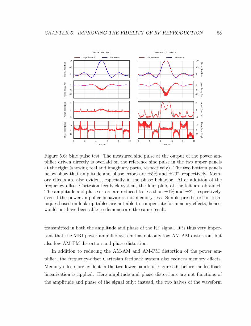
CHAPTER 5. IMPROVING THE FIDELITY OF RF REPRODUCTION 88
WITH CONTROL WITHOUT CONTROL
ReferenceExperimental
-5
0
5 Am
pl. Error [%]
0 2 4 6 8 10Time, ms
-10
0
10
Phase Error [deg]
Time, ms
Norm
. Real Part
Norm
. Imag. Part
ReferenceExperimental
Am
pl. E
rror
[%]
Phas
e Er
ror [
deg]
Nor
m. R
eal P
art
Nor
m. I
mag
. Par
t
0
0.5
-0.2
-0.1
0
-5
0
5
-10
0
10
1.0
0
0.5
-0.2
-0.1
0
1.0
0 2 4 6 8 10
Figure 5.6: Sinc pulse test. The measured sinc pulse at the output of the power am-plifier driven directly is overlaid on the reference sinc pulse in the two upper panelsat the right (showing real and imaginary parts, respectively). The two bottom panelsbelow show that amplitude and phase errors are ±5% and ±20, respectively. Mem-ory effects are also evident, especially in the phase behavior. After addition of thefrequency-offset Cartesian feedback system, the four plots at the left are obtained.The amplitude and phase errors are reduced to less than ±1% and ±2, respectively,even if the power amplifier behavior is not memory-less. Simple pre-distortion tech-niques based on look-up tables are not able to compensate for memory effects, hence,would not have been able to demonstrate the same result.
transmitted in both the amplitude and phase of the RF signal. It is thus very impor-
tant that the MRI power amplifier system has not only low AM-AM distortion, but
also low AM-PM distortion and phase distortion.
In addition to reducing the AM-AM and AM-PM distortion of the power am-
plifier, the frequency-offset Cartesian feedback system also reduces memory effects.
Memory effects are evident in the two lower panels of Figure 5.6, before the feedback
linearization is applied. Here amplitude and phase distortions are not functions of
the amplitude and phase of the signal only: instead, the two halves of the waveform
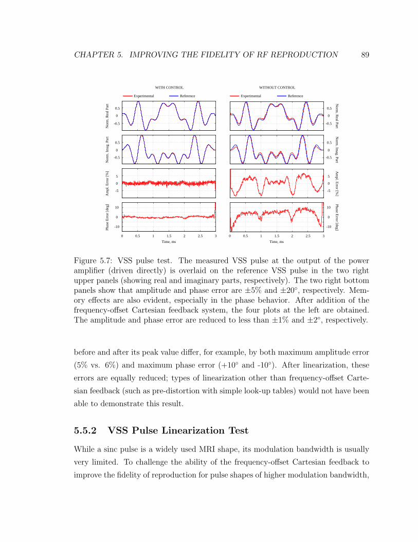
CHAPTER 5. IMPROVING THE FIDELITY OF RF REPRODUCTION 89
Abs(TX) Error
-0.5
0
0.5
ReferenceExperimental
-0.5
0
0.5
-5
0
5
Am
pl. Error [%]
0 0.5 1 1.5 2 2.5 3Time, ms
0.5 1 1.5 2 2.5 3
-10
0
10
Phase Error [deg]
Time, ms
Ph(RX)-Ph(TX) Error
Norm
. Real Part
Norm
. Imag. Part
ReferenceExperimental
Am
pl. E
rror
[%]
Phas
e Er
ror [
deg]
Nor
m. R
eal P
art
Nor
m. I
mag
. Par
t
-0.5
0
0.5
-0.5
0
0.5
-5
0
5
-10
0
10
0
WITH CONTROL WITHOUT CONTROL
Figure 5.7: VSS pulse test. The measured VSS pulse at the output of the poweramplifier (driven directly) is overlaid on the reference VSS pulse in the two rightupper panels (showing real and imaginary parts, respectively). The two right bottompanels show that amplitude and phase error are ±5% and ±20, respectively. Mem-ory effects are also evident, especially in the phase behavior. After addition of thefrequency-offset Cartesian feedback system, the four plots at the left are obtained.The amplitude and phase error are reduced to less than ±1% and ±2, respectively.
before and after its peak value differ, for example, by both maximum amplitude error
(5% vs. 6%) and maximum phase error (+10 and -10). After linearization, these
errors are equally reduced; types of linearization other than frequency-offset Carte-
sian feedback (such as pre-distortion with simple look-up tables) would not have been
able to demonstrate this result.
5.5.2 VSS Pulse Linearization Test
While a sinc pulse is a widely used MRI shape, its modulation bandwidth is usually
very limited. To challenge the ability of the frequency-offset Cartesian feedback to
improve the fidelity of reproduction for pulse shapes of higher modulation bandwidth,
CHAPTER 5. IMPROVING THE FIDELITY OF RF REPRODUCTION 90
a similar test was performed with a Very Selective Saturation (VSS) pulse as the
reference signal [67, 77].
Unlike conventional Shinnar-Le Roux (SLR) pulses [62], VSS pulses are quadratic
phase modulated (linear frequency sweep) as well as amplitude modulated to spread
the energy evenly throughout the entire pulse duration. Despite their short dura-
tion and small in-band equi-ripple (equal amplitude), they possess large excitation
bandwidths and narrow transition bands (sharper edge profiles) useful, for exam-
ple, to overcome the geometric restrictions in volume prescription and chemical shift
registration errors in MRI spectroscopy.
The VSS pulse used in this test had 5 kHz excitation bandwidth. Figure 5.7
compares the results of driving the power amplifier directly and adding the frequency-
offset Cartesian feedback system to the same amplifier. Despite the larger modulation
bandwidth, the system shows performance similar to that demonstrated for the case
of a sinc pulse. The amplitude distortion is reduced from over ±5% (power amplifier
only) to less than ±1% (after addition of the feedback system). The phase error is
reduced from ±10 to less than ±2. Also in this case, memory effects are evident in
the behavior of the power amplifier and are significantly attenuated by the action of
the loop.
5.6 Effect of Linearization on Magnetization
Once the waveshape of a pulse is known, it is possible to calculate the effect that the
pulse has on the magnetization using the Bloch equations [76].
The Bloch equations are a set of coupled differential equations that can be used
to describe the behavior of the magnetization vector under any conditions. Let ~M(t)
be the nuclear magnetization, γ the gyromagnetic ratio, and ~B(t) the total magnetic
field. Then, the Bloch equations are
dMx(t)
dt= γ( ~M(t)× ~B(t))x −
Mx(t)
T2
(5.6)
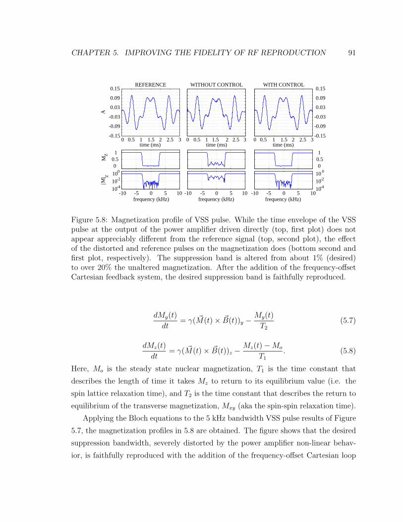
CHAPTER 5. IMPROVING THE FIDELITY OF RF REPRODUCTION 91
00.5
1
MZ
10-410-2100
||
0 0.5 1 1.5 2 2.5 3-0.15
-0.09
-0.03
0.03
0.09
0.15
time (ms)
frequency (kHz)-10 -5 0 5 10
-0.15
-0.09
-0.03
0.03
0.09
0.15
MZ
A
00.51
10-410-210 0
0 0.5 1 1.5 2 2.5 3time (ms)
0 0.5 1 1.5 2 2.5 3time (ms)
frequency (kHz)-10 -5 0 5 10
frequency (kHz)-10 -5 0 5 10
WITH CONTROLWITHOUT CONTROLREFERENCE
Figure 5.8: Magnetization profile of VSS pulse. While the time envelope of the VSSpulse at the output of the power amplifier driven directly (top, first plot) does notappear appreciably different from the reference signal (top, second plot), the effectof the distorted and reference pulses on the magnetization does (bottom second andfirst plot, respectively). The suppression band is altered from about 1% (desired)to over 20% the unaltered magnetization. After the addition of the frequency-offsetCartesian feedback system, the desired suppression band is faithfully reproduced.
dMy(t)
dt= γ( ~M(t)× ~B(t))y −
My(t)
T2
(5.7)
dMz(t)
dt= γ( ~M(t)× ~B(t))z −
Mz(t)−Mo
T1
. (5.8)
Here, Mo is the steady state nuclear magnetization, T1 is the time constant that
describes the length of time it takes Mz to return to its equilibrium value (i.e. the
spin lattice relaxation time), and T2 is the time constant that describes the return to
equilibrium of the transverse magnetization, Mxy (aka the spin-spin relaxation time).
Applying the Bloch equations to the 5 kHz bandwidth VSS pulse results of Figure
5.7, the magnetization profiles in 5.8 are obtained. The figure shows that the desired
suppression bandwidth, severely distorted by the power amplifier non-linear behav-
ior, is faithfully reproduced with the addition of the frequency-offset Cartesian loop
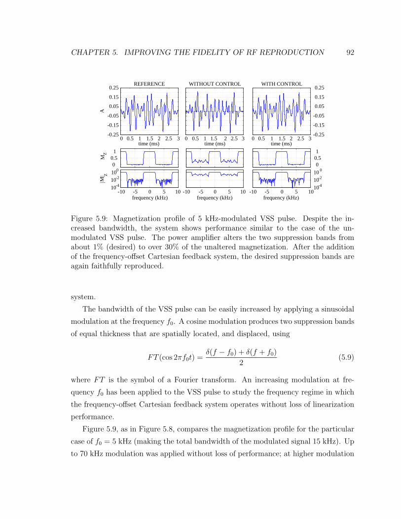
CHAPTER 5. IMPROVING THE FIDELITY OF RF REPRODUCTION 92
-0.25
-0.15
-0.05
0.05
0.15
0.25
-0.25
-0.15
-0.05
0.05
0.15
0.25
00.5
1
MZ
10-410-2100
||
0 0.5 1 1.5 2 2.5 3time (ms)
frequency (kHz)-10 -5 0 5 10
MZ
A
00.51
10-410-210 0
0 0.5 1 1.5 2 2.5 3time (ms)
0 0.5 1 1.5 2 2.5 3time (ms)
frequency (kHz)-10 -5 0 5 10
frequency (kHz)-10 -5 0 5 10
WITH CONTROLWITHOUT CONTROLREFERENCE
Figure 5.9: Magnetization profile of 5 kHz-modulated VSS pulse. Despite the in-creased bandwidth, the system shows performance similar to the case of the un-modulated VSS pulse. The power amplifier alters the two suppression bands fromabout 1% (desired) to over 30% of the unaltered magnetization. After the additionof the frequency-offset Cartesian feedback system, the desired suppression bands areagain faithfully reproduced.
system.
The bandwidth of the VSS pulse can be easily increased by applying a sinusoidal
modulation at the frequency f0. A cosine modulation produces two suppression bands
of equal thickness that are spatially located, and displaced, using
FT (cos 2πf0t) =δ(f − f0) + δ(f + f0)
2(5.9)
where FT is the symbol of a Fourier transform. An increasing modulation at fre-
quency f0 has been applied to the VSS pulse to study the frequency regime in which
the frequency-offset Cartesian feedback system operates without loss of linearization
performance.
Figure 5.9, as in Figure 5.8, compares the magnetization profile for the particular
case of f0 = 5 kHz (making the total bandwidth of the modulated signal 15 kHz). Up
to 70 kHz modulation was applied without loss of performance; at higher modulation
CHAPTER 5. IMPROVING THE FIDELITY OF RF REPRODUCTION 93
bandwidth, the linearization effect of the loop is lower, consistent with the slow roll-off
of the error amplification created by the polyphase amplifiers.
5.7 Closed Loop Image Rejection Performance
The ability of the frequency-offset Cartesian feedback system to reject negative fre-
quencies is an important figure of merit, as it describes its robustness to the undesired
quadrature mismatches created by the down-mixer and other components of the feed-
back path that may corrupt the desired signal. For this reason, the lower sideband
rejection of the closed-loop system in a 400 kHz span at the center frequency of the
polyphase difference amplifiers (64.5 MHz) has been measured.
Table 5.1 shows the results of this measurement. The sideband rejection of the
closed-loop frequency-offset Cartesian feedback system is highest at 64.5 MHz and,
as expected, is close to the sideband rejection of the polyphase difference amplifiers
measured in the previous experiment (described in Chapter 3). The difference be-
tween the values in this and the previous experiment results from image (negative
frequency) generation by the error and reference input quadrature down-converters,
which are then amplified unequally by the desired polyphase response to negative in-
put frequencies. In this manner, besides mismatches in the quadrature up-converter,
image rejection limits by quadrature down-conversion can translate to sideband gen-
eration. The same argument can be made regarding the observation that the sideband
rejection decreases more rapidly at frequencies lower than 64.5 MHz.
5.8 Summary
In this chapter, the nature of the distortion created by the behavior of any RF power
amplifier has been discussed and the ability of the feedback system to improve the
fidelity of RF reproduction has been demonstrated with different feedback control
loop variables and power amplifiers. Notably, excellent performance is obtained with
much relaxed specifications for the transmitter with respect to conventional Cartesian
feedback systems, thanks to the use of polyphase loop error amplifiers.
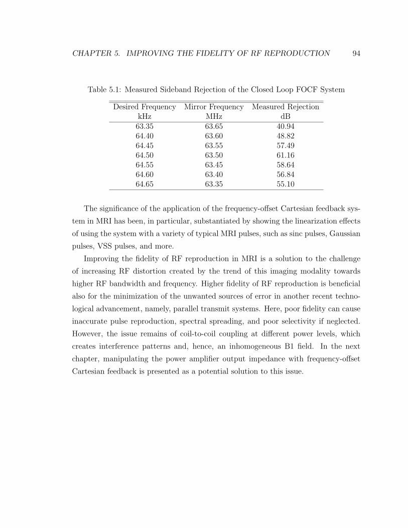
CHAPTER 5. IMPROVING THE FIDELITY OF RF REPRODUCTION 94
Table 5.1: Measured Sideband Rejection of the Closed Loop FOCF System
Desired Frequency Mirror Frequency Measured RejectionkHz MHz dB
63.35 63.65 40.9464.40 63.60 48.8264.45 63.55 57.4964.50 63.50 61.1664.55 63.45 58.6464.60 63.40 56.8464.65 63.35 55.10
The significance of the application of the frequency-offset Cartesian feedback sys-
tem in MRI has been, in particular, substantiated by showing the linearization effects
of using the system with a variety of typical MRI pulses, such as sinc pulses, Gaussian
pulses, VSS pulses, and more.
Improving the fidelity of RF reproduction in MRI is a solution to the challenge
of increasing RF distortion created by the trend of this imaging modality towards
higher RF bandwidth and frequency. Higher fidelity of RF reproduction is beneficial
also for the minimization of the unwanted sources of error in another recent techno-
logical advancement, namely, parallel transmit systems. Here, poor fidelity can cause
inaccurate pulse reproduction, spectral spreading, and poor selectivity if neglected.
However, the issue remains of coil-to-coil coupling at different power levels, which
creates interference patterns and, hence, an inhomogeneous B1 field. In the next
chapter, manipulating the power amplifier output impedance with frequency-offset
Cartesian feedback is presented as a potential solution to this issue.
Chapter 6
Manipulating the Amplifier
Impedance
6.1 Introduction
Coupling between coil elements of a transmit array is one of the key challenges faced
by designers of MRI transmitter arrays. As discussed in this chapter, different meth-
ods of dealing with the challenge have been presented in the literature. The alter-
native method proposed and motivated in this dissertation consists of manipulating
the output impedance of the RF power amplifier using frequency-offset Cartesian
feedback.
The chapter describes the theory behind impedance manipulation, providing an
understanding of how this manipulation can be obtained electronically using the
feedback method and system described in the previous chapters. The results of sim-
ulations based on this mathematical analysis are also presented. Then, the “load
pull” method and setup is also presented, which was added to the frequency-offset
Cartesian feedback system described in Chapter 4 to measure the output impedance
of the power amplifier under transmit power conditions.
Finally, the results of electronically manipulating the output impedance of both
single amplifiers (with and without terminating circulator) and balanced amplifiers
are presented, which demonstrate the ability to predictably manipulate the real and
95
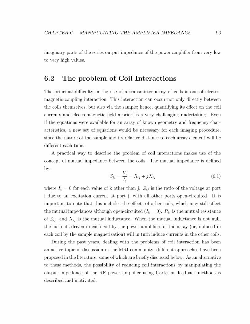
CHAPTER 6. MANIPULATING THE AMPLIFIER IMPEDANCE 96
imaginary parts of the series output impedance of the power amplifier from very low
to very high values.
6.2 The problem of Coil Interactions
The principal difficulty in the use of a transmitter array of coils is one of electro-
magnetic coupling interaction. This interaction can occur not only directly between
the coils themselves, but also via the sample; hence, quantifying its effect on the coil
currents and electromagnetic field a priori is a very challenging undertaking. Even
if the equations were available for an array of known geometry and frequency char-
acteristics, a new set of equations would be necessary for each imaging procedure,
since the nature of the sample and its relative distance to each array element will be
different each time.
A practical way to describe the problem of coil interactions makes use of the
concept of mutual impedance between the coils. The mutual impedance is defined
by:
Zij =ViIj
= Rij + jXij (6.1)
where Ik = 0 for each value of k other than j. Zij is the ratio of the voltage at port
i due to an excitation current at port j, with all other ports open-circuited. It is
important to note that this includes the effects of other coils, which may still affect
the mutual impedances although open-circuited (Ik = 0). Rij is the mutual resistance
of Zij, and Xij is the mutual inductance. When the mutual inductance is not null,
the currents driven in each coil by the power amplifiers of the array (or, induced in
each coil by the sample magnetization) will in turn induce currents in the other coils.
During the past years, dealing with the problems of coil interaction has been
an active topic of discussion in the MRI community; different approaches have been
proposed in the literature, some of which are briefly discussed below. As an alternative
to these methods, the possibility of reducing coil interactions by manipulating the
output impedance of the RF power amplifier using Cartesian feedback methods is
described and motivated.
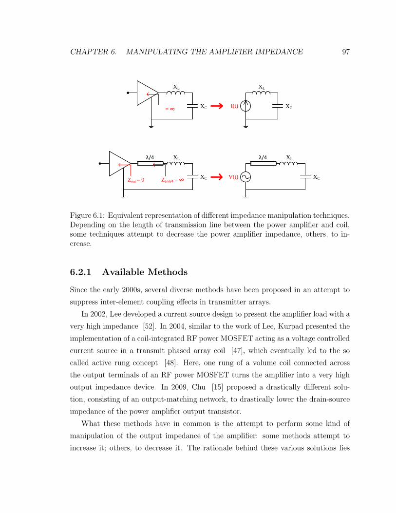
CHAPTER 6. MANIPULATING THE AMPLIFIER IMPEDANCE 97
=
== 0
XL
XC I(t)
XL
XCZout
λ/4
Z@λ/4
XL
XC
XL
XC
λ/4
V(t)
Figure 6.1: Equivalent representation of different impedance manipulation techniques.Depending on the length of transmission line between the power amplifier and coil,some techniques attempt to decrease the power amplifier impedance, others, to in-crease.
6.2.1 Available Methods
Since the early 2000s, several diverse methods have been proposed in an attempt to
suppress inter-element coupling effects in transmitter arrays.
In 2002, Lee developed a current source design to present the amplifier load with a
very high impedance [52]. In 2004, similar to the work of Lee, Kurpad presented the
implementation of a coil-integrated RF power MOSFET acting as a voltage controlled
current source in a transmit phased array coil [47], which eventually led to the so
called active rung concept [48]. Here, one rung of a volume coil connected across
the output terminals of an RF power MOSFET turns the amplifier into a very high
output impedance device. In 2009, Chu [15] proposed a drastically different solu-
tion, consisting of an output-matching network, to drastically lower the drain-source
impedance of the power amplifier output transistor.
What these methods have in common is the attempt to perform some kind of
manipulation of the output impedance of the amplifier: some methods attempt to
increase it; others, to decrease it. The rationale behind these various solutions lies
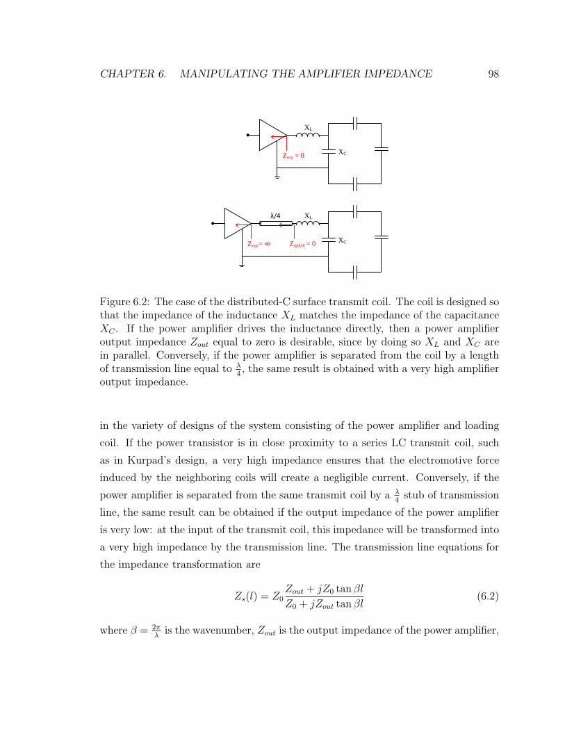
CHAPTER 6. MANIPULATING THE AMPLIFIER IMPEDANCE 98
XL
XCZout
XL
XCZout
λ/4
=
= 0
Z@λ/4 = 0
Figure 6.2: The case of the distributed-C surface transmit coil. The coil is designed sothat the impedance of the inductance XL matches the impedance of the capacitanceXC . If the power amplifier drives the inductance directly, then a power amplifieroutput impedance Zout equal to zero is desirable, since by doing so XL and XC arein parallel. Conversely, if the power amplifier is separated from the coil by a lengthof transmission line equal to λ
4, the same result is obtained with a very high amplifier
output impedance.
in the variety of designs of the system consisting of the power amplifier and loading
coil. If the power transistor is in close proximity to a series LC transmit coil, such
as in Kurpad’s design, a very high impedance ensures that the electromotive force
induced by the neighboring coils will create a negligible current. Conversely, if the
power amplifier is separated from the same transmit coil by a λ4
stub of transmission
line, the same result can be obtained if the output impedance of the power amplifier
is very low: at the input of the transmit coil, this impedance will be transformed into
a very high impedance by the transmission line. The transmission line equations for
the impedance transformation are
Zs(l) = Z0Zout + jZ0 tan βl
Z0 + jZout tan βl(6.2)
where β = 2πλ
is the wavenumber, Zout is the output impedance of the power amplifier,
CHAPTER 6. MANIPULATING THE AMPLIFIER IMPEDANCE 99
XL
XC
Zin
XL
XC
is a short circuit
(ideally)
PIN diode
Figure 6.3: MRI receive technologies. A PIN diode (bottom, during the transmitinterval) or a properly-matched preamplifier input impedance (top, during the re-ceive interval) presents a short-circuit to the surface receive coil. If XL = XC , thisshort-circuit allows the tank circuit inductor and capacitor to create a very high in-put impedance, which open-circuits the coil. Methods of dealing with transmit coilinteractions based on power amplifier impedance manipulation attempt to emulatethese “Q-spoiling” techniques.
and Zs is the impedance seen by the transmit coil separated from the power amplifier
by a transmission line of length l and characteristic impedance Z0. Z0 is defined as
the coaxial characteristic impedance. If l is null, then
Zs(l) = Zout (6.3)
and to minimize induced currents, Zout should be very high. If l is λ4, then
Zs(l) =Z2
0
Zout(6.4)
and to minimize induced currents, Zout should be very low (Zs should be high). See
Figure 6.1.
If the transmit coil is as shown in Chapter 4 (a distributed-C surface transmit
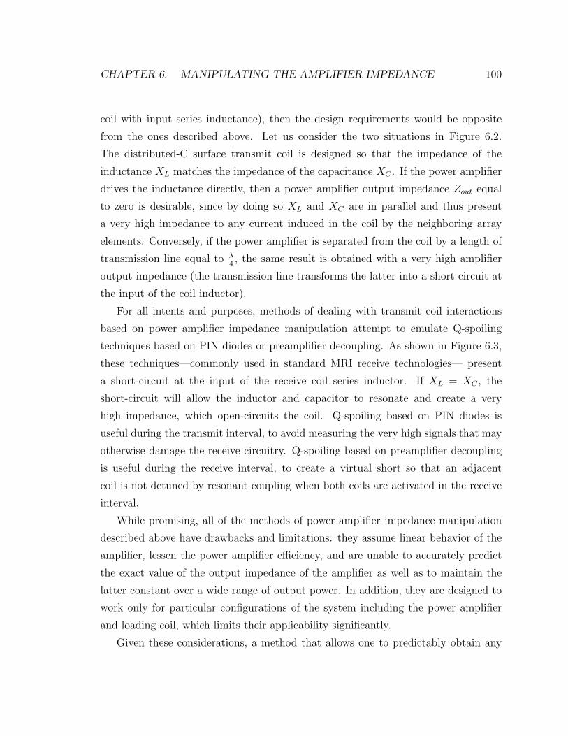
CHAPTER 6. MANIPULATING THE AMPLIFIER IMPEDANCE 100
coil with input series inductance), then the design requirements would be opposite
from the ones described above. Let us consider the two situations in Figure 6.2.
The distributed-C surface transmit coil is designed so that the impedance of the
inductance XL matches the impedance of the capacitance XC . If the power amplifier
drives the inductance directly, then a power amplifier output impedance Zout equal
to zero is desirable, since by doing so XL and XC are in parallel and thus present
a very high impedance to any current induced in the coil by the neighboring array
elements. Conversely, if the power amplifier is separated from the coil by a length of
transmission line equal to λ4, the same result is obtained with a very high amplifier
output impedance (the transmission line transforms the latter into a short-circuit at
the input of the coil inductor).
For all intents and purposes, methods of dealing with transmit coil interactions
based on power amplifier impedance manipulation attempt to emulate Q-spoiling
techniques based on PIN diodes or preamplifier decoupling. As shown in Figure 6.3,
these techniques—commonly used in standard MRI receive technologies— present
a short-circuit at the input of the receive coil series inductor. If XL = XC , the
short-circuit will allow the inductor and capacitor to resonate and create a very
high impedance, which open-circuits the coil. Q-spoiling based on PIN diodes is
useful during the transmit interval, to avoid measuring the very high signals that may
otherwise damage the receive circuitry. Q-spoiling based on preamplifier decoupling
is useful during the receive interval, to create a virtual short so that an adjacent
coil is not detuned by resonant coupling when both coils are activated in the receive
interval.
While promising, all of the methods of power amplifier impedance manipulation
described above have drawbacks and limitations: they assume linear behavior of the
amplifier, lessen the power amplifier efficiency, and are unable to accurately predict
the exact value of the output impedance of the amplifier as well as to maintain the
latter constant over a wide range of output power. In addition, they are designed to
work only for particular configurations of the system including the power amplifier
and loading coil, which limits their applicability significantly.
Given these considerations, a method that allows one to predictably obtain any
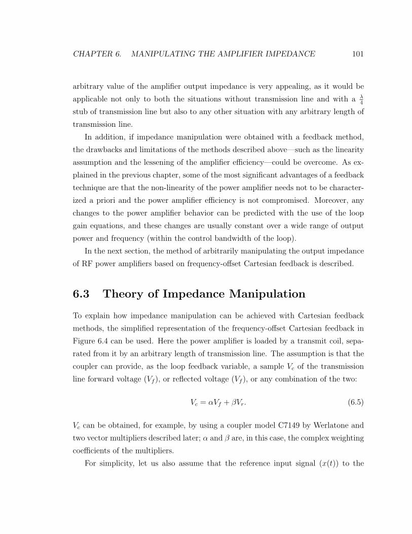
CHAPTER 6. MANIPULATING THE AMPLIFIER IMPEDANCE 101
arbitrary value of the amplifier output impedance is very appealing, as it would be
applicable not only to both the situations without transmission line and with a λ4
stub of transmission line but also to any other situation with any arbitrary length of
transmission line.
In addition, if impedance manipulation were obtained with a feedback method,
the drawbacks and limitations of the methods described above—such as the linearity
assumption and the lessening of the amplifier efficiency—could be overcome. As ex-
plained in the previous chapter, some of the most significant advantages of a feedback
technique are that the non-linearity of the power amplifier needs not to be character-
ized a priori and the power amplifier efficiency is not compromised. Moreover, any
changes to the power amplifier behavior can be predicted with the use of the loop
gain equations, and these changes are usually constant over a wide range of output
power and frequency (within the control bandwidth of the loop).
In the next section, the method of arbitrarily manipulating the output impedance
of RF power amplifiers based on frequency-offset Cartesian feedback is described.
6.3 Theory of Impedance Manipulation
To explain how impedance manipulation can be achieved with Cartesian feedback
methods, the simplified representation of the frequency-offset Cartesian feedback in
Figure 6.4 can be used. Here the power amplifier is loaded by a transmit coil, sepa-
rated from it by an arbitrary length of transmission line. The assumption is that the
coupler can provide, as the loop feedback variable, a sample Vc of the transmission
line forward voltage (Vf ), or reflected voltage (Vf ), or any combination of the two:
Vc = αVf + βVr. (6.5)
Vc can be obtained, for example, by using a coupler model C7149 by Werlatone and
two vector multipliers described later; α and β are, in this case, the complex weighting
coefficients of the multipliers.
For simplicity, let us also assume that the reference input signal (x(t)) to the
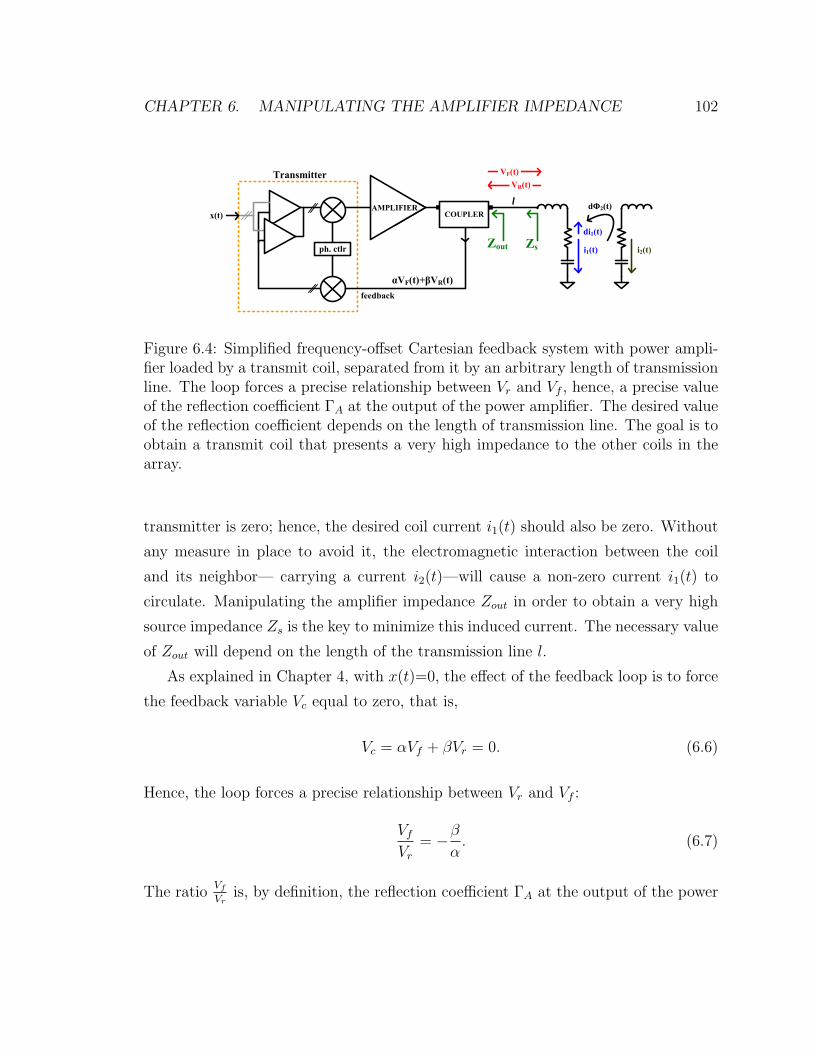
CHAPTER 6. MANIPULATING THE AMPLIFIER IMPEDANCE 102
out
x(t)
feedback
Transmitter
COUPLER
ph. ctlr
AMPLIFIER
i1(t) i2(t)
dΦ2(t)
αVF(t)+βVR(t)
VF(t)VR(t)
l
di1(t)
s
Figure 6.4: Simplified frequency-offset Cartesian feedback system with power ampli-fier loaded by a transmit coil, separated from it by an arbitrary length of transmissionline. The loop forces a precise relationship between Vr and Vf , hence, a precise valueof the reflection coefficient ΓA at the output of the power amplifier. The desired valueof the reflection coefficient depends on the length of transmission line. The goal is toobtain a transmit coil that presents a very high impedance to the other coils in thearray.
transmitter is zero; hence, the desired coil current i1(t) should also be zero. Without
any measure in place to avoid it, the electromagnetic interaction between the coil
and its neighbor— carrying a current i2(t)—will cause a non-zero current i1(t) to
circulate. Manipulating the amplifier impedance Zout in order to obtain a very high
source impedance Zs is the key to minimize this induced current. The necessary value
of Zout will depend on the length of the transmission line l.
As explained in Chapter 4, with x(t)=0, the effect of the feedback loop is to force
the feedback variable Vc equal to zero, that is,
Vc = αVf + βVr = 0. (6.6)
Hence, the loop forces a precise relationship between Vr and Vf :
VfVr
= −βα. (6.7)
The ratioVf
Vris, by definition, the reflection coefficient ΓA at the output of the power

CHAPTER 6. MANIPULATING THE AMPLIFIER IMPEDANCE 103
amplifier, which is also described as
ΓA =VfVr
=Zout − Z0
Zout + Z0
(6.8)
where Z0 is the impedance of the coupler (approximately 50 Ω). In summary, weight-
ing the transmission line voltages with coefficients α and β synthesizes an impedance
at the output of the power amplifier described by
Zout = Z01 + ΓA1− ΓA
= Z0
1− βα
1 + βα
(6.9)
which can be tuned in order to obtain a very high impedance Zs(l) using the trans-
mission line equation.
If, for example, l is zero, then Zout should be very high—ideally, infinite; hence,
the denominator of Eq. 6.9 should be zero and
ΓA = −βα
= 1. (6.10)
If instead l is a quarter wave length, then Zout should be very low—ideally, zero;
hence,
ΓA = −βα
= −1. (6.11)
In summary, choosing the weighted combination αVf + βVr as the feedback variable
of the frequency-offset Cartesian feedback allows manipulating the output impedance
of the power amplifier in order to obtain a value that depends only on the ratio of
the two weighting coefficients.
6.4 Load Pull Setup
To characterize the power amplifier impedance behavior under transmit power condi-
tions, the automated load-pull and hot S22 described by Scott [69] was used. Mea-
surements are based on the concept of a nonlinear Thevenin circuit in which equiva-
lent open circuit output voltage and output series impedance can be assigned at each
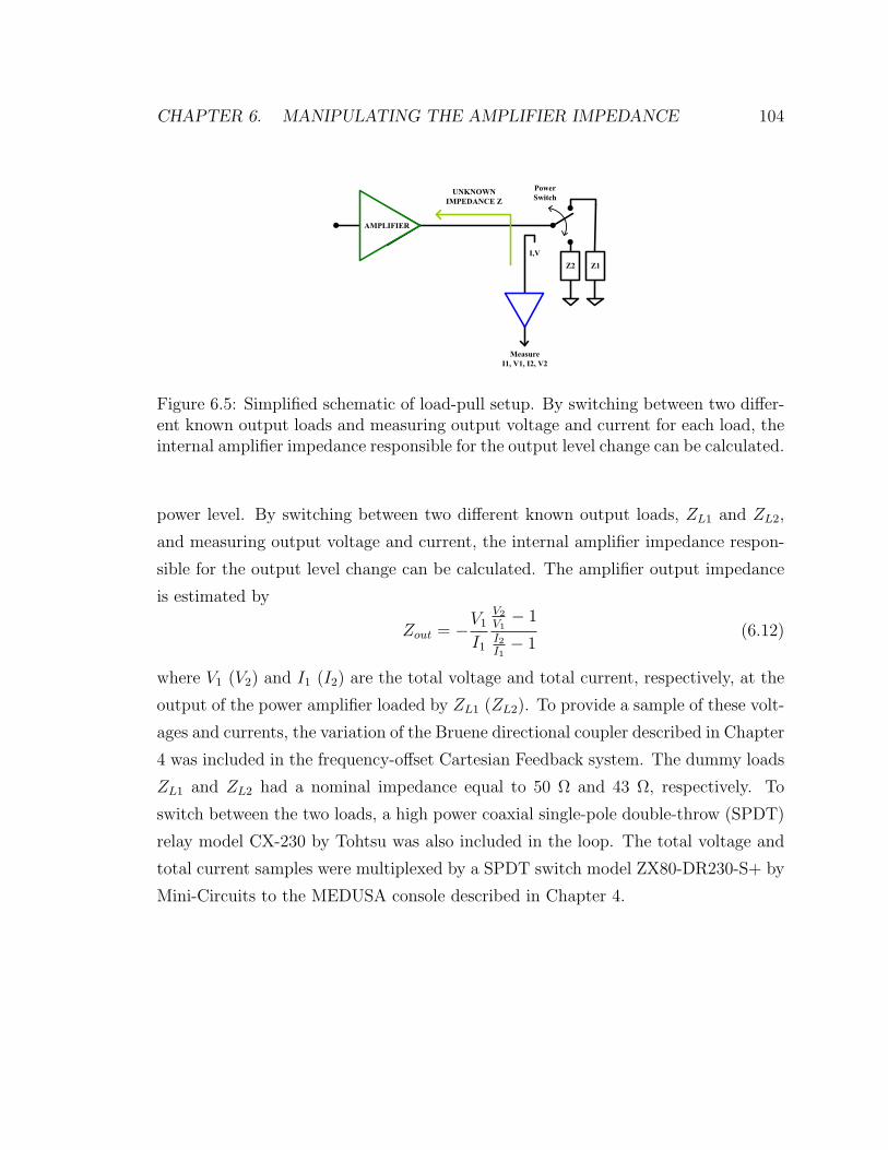
CHAPTER 6. MANIPULATING THE AMPLIFIER IMPEDANCE 104
Figure 6.5: Simplified schematic of load-pull setup. By switching between two differ-ent known output loads and measuring output voltage and current for each load, theinternal amplifier impedance responsible for the output level change can be calculated.
power level. By switching between two different known output loads, ZL1 and ZL2,
and measuring output voltage and current, the internal amplifier impedance respon-
sible for the output level change can be calculated. The amplifier output impedance
is estimated by
Zout = −V1
I1
V2
V1− 1
I2I1− 1
(6.12)
where V1 (V2) and I1 (I2) are the total voltage and total current, respectively, at the
output of the power amplifier loaded by ZL1 (ZL2). To provide a sample of these volt-
ages and currents, the variation of the Bruene directional coupler described in Chapter
4 was included in the frequency-offset Cartesian Feedback system. The dummy loads
ZL1 and ZL2 had a nominal impedance equal to 50 Ω and 43 Ω, respectively. To
switch between the two loads, a high power coaxial single-pole double-throw (SPDT)
relay model CX-230 by Tohtsu was also included in the loop. The total voltage and
total current samples were multiplexed by a SPDT switch model ZX80-DR230-S+ by
Mini-Circuits to the MEDUSA console described in Chapter 4.
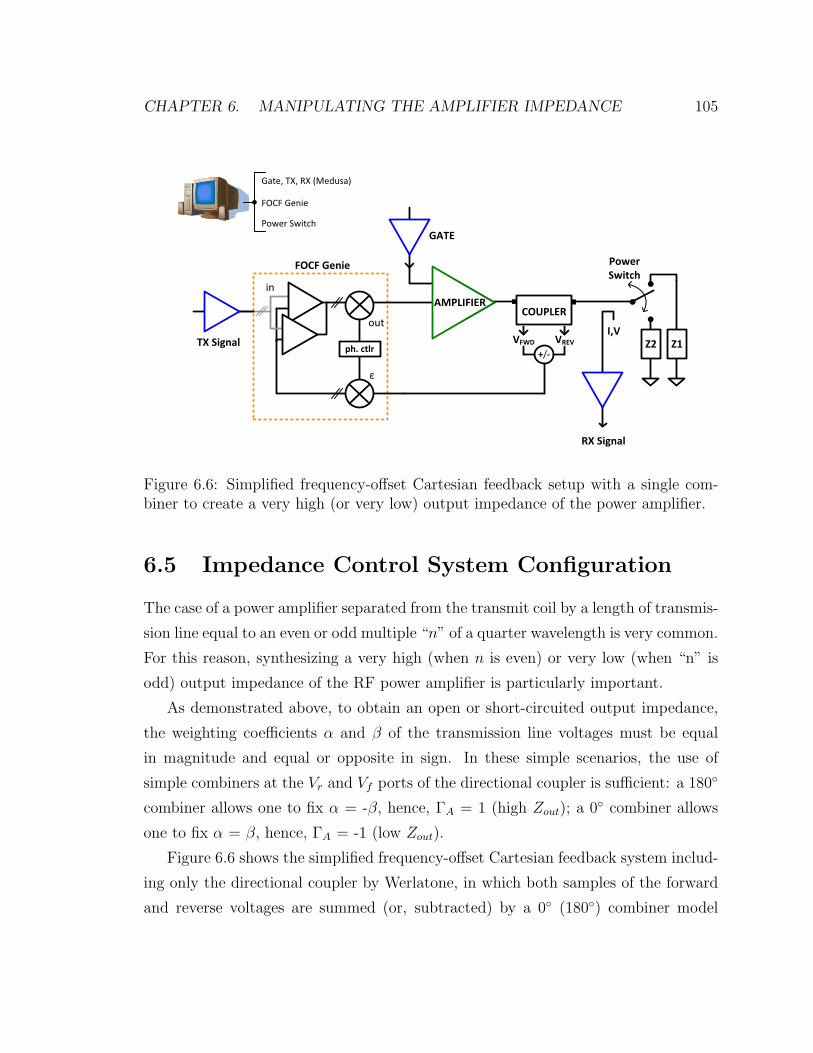
CHAPTER 6. MANIPULATING THE AMPLIFIER IMPEDANCE 105
Figure 6.6: Simplified frequency-offset Cartesian feedback setup with a single com-biner to create a very high (or very low) output impedance of the power amplifier.
6.5 Impedance Control System Configuration
The case of a power amplifier separated from the transmit coil by a length of transmis-
sion line equal to an even or odd multiple “n” of a quarter wavelength is very common.
For this reason, synthesizing a very high (when n is even) or very low (when “n” is
odd) output impedance of the RF power amplifier is particularly important.
As demonstrated above, to obtain an open or short-circuited output impedance,
the weighting coefficients α and β of the transmission line voltages must be equal
in magnitude and equal or opposite in sign. In these simple scenarios, the use of
simple combiners at the Vr and Vf ports of the directional coupler is sufficient: a 180
combiner allows one to fix α = -β, hence, ΓA = 1 (high Zout); a 0 combiner allows
one to fix α = β, hence, ΓA = -1 (low Zout).
Figure 6.6 shows the simplified frequency-offset Cartesian feedback system includ-
ing only the directional coupler by Werlatone, in which both samples of the forward
and reverse voltages are summed (or, subtracted) by a 0 (180) combiner model
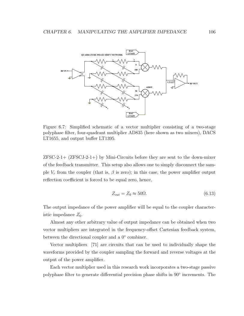
CHAPTER 6. MANIPULATING THE AMPLIFIER IMPEDANCE 106
Figure 6.7: Simplified schematic of a vector multiplier consisting of a two-stagepolyphase filter, four-quadrant multiplier AD835 (here shown as two mixers), DACSLT1655, and output buffer LT1395.
ZFSC-2-1+ (ZFSCJ-2-1+) by Mini-Circuits before they are sent to the down-mixer
of the feedback transmitter. This setup also allows one to simply disconnect the sam-
ple Vr from the coupler (that is, β is zero); in this case, the power amplifier output
reflection coefficient is forced to be equal zero, hence,
Zout = Z0 ≈ 50Ω. (6.13)
The output impedance of the power amplifier will be equal to the coupler character-
istic impedance Z0.
Almost any other arbitrary value of output impedance can be obtained when two
vector multipliers are integrated in the frequency-offset Cartesian feedback system,
between the directional coupler and a 0 combiner.
Vector multipliers [71] are circuits that can be used to individually shape the
waveforms provided by the coupler sampling the forward and reverse voltages at the
output of the power amplifier.
Each vector multiplier used in this research work incorporates a two-stage passive
polyphase filter to generate differential precision phase shifts in 90 increments. The
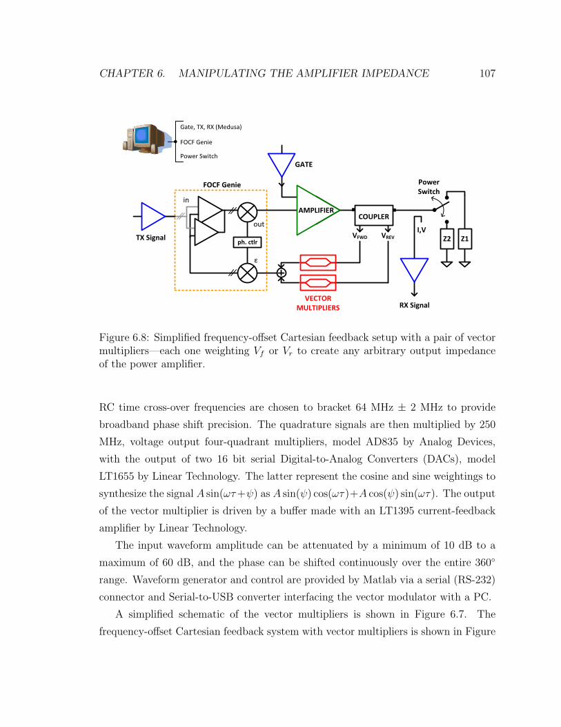
CHAPTER 6. MANIPULATING THE AMPLIFIER IMPEDANCE 107
Figure 6.8: Simplified frequency-offset Cartesian feedback setup with a pair of vectormultipliers—each one weighting Vf or Vr to create any arbitrary output impedanceof the power amplifier.
RC time cross-over frequencies are chosen to bracket 64 MHz ± 2 MHz to provide
broadband phase shift precision. The quadrature signals are then multiplied by 250
MHz, voltage output four-quadrant multipliers, model AD835 by Analog Devices,
with the output of two 16 bit serial Digital-to-Analog Converters (DACs), model
LT1655 by Linear Technology. The latter represent the cosine and sine weightings to
synthesize the signal A sin(ωτ+ψ) as A sin(ψ) cos(ωτ)+A cos(ψ) sin(ωτ). The output
of the vector multiplier is driven by a buffer made with an LT1395 current-feedback
amplifier by Linear Technology.
The input waveform amplitude can be attenuated by a minimum of 10 dB to a
maximum of 60 dB, and the phase can be shifted continuously over the entire 360
range. Waveform generator and control are provided by Matlab via a serial (RS-232)
connector and Serial-to-USB converter interfacing the vector modulator with a PC.
A simplified schematic of the vector multipliers is shown in Figure 6.7. The
frequency-offset Cartesian feedback system with vector multipliers is shown in Figure
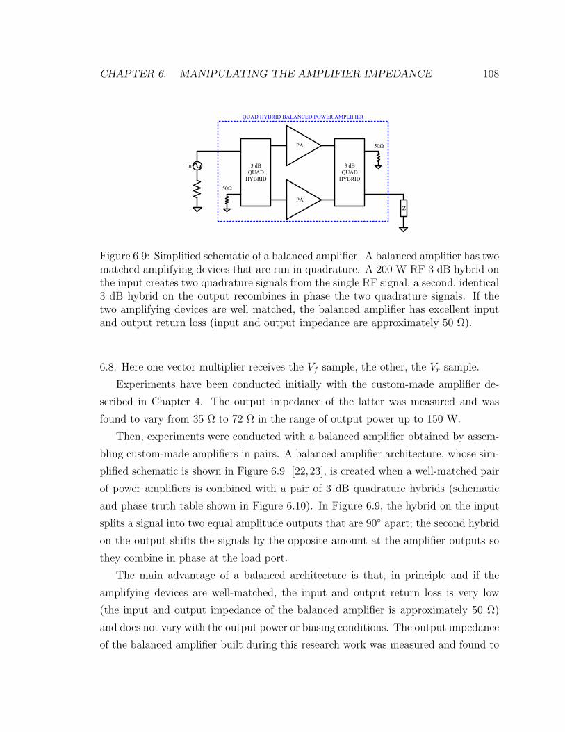
CHAPTER 6. MANIPULATING THE AMPLIFIER IMPEDANCE 108
error
3 dBQUAD
HYBRID
3 dBQUAD
HYBRID
50Ω
50Ω
QUAD HYBRID BALANCED POWER AMPLIFIER
in
Z
PA
PA
Figure 6.9: Simplified schematic of a balanced amplifier. A balanced amplifier has twomatched amplifying devices that are run in quadrature. A 200 W RF 3 dB hybrid onthe input creates two quadrature signals from the single RF signal; a second, identical3 dB hybrid on the output recombines in phase the two quadrature signals. If thetwo amplifying devices are well matched, the balanced amplifier has excellent inputand output return loss (input and output impedance are approximately 50 Ω).
6.8. Here one vector multiplier receives the Vf sample, the other, the Vr sample.
Experiments have been conducted initially with the custom-made amplifier de-
scribed in Chapter 4. The output impedance of the latter was measured and was
found to vary from 35 Ω to 72 Ω in the range of output power up to 150 W.
Then, experiments were conducted with a balanced amplifier obtained by assem-
bling custom-made amplifiers in pairs. A balanced amplifier architecture, whose sim-
plified schematic is shown in Figure 6.9 [22,23], is created when a well-matched pair
of power amplifiers is combined with a pair of 3 dB quadrature hybrids (schematic
and phase truth table shown in Figure 6.10). In Figure 6.9, the hybrid on the input
splits a signal into two equal amplitude outputs that are 90 apart; the second hybrid
on the output shifts the signals by the opposite amount at the amplifier outputs so
they combine in phase at the load port.
The main advantage of a balanced architecture is that, in principle and if the
amplifying devices are well-matched, the input and output return loss is very low
(the input and output impedance of the balanced amplifier is approximately 50 Ω)
and does not vary with the output power or biasing conditions. The output impedance
of the balanced amplifier built during this research work was measured and found to
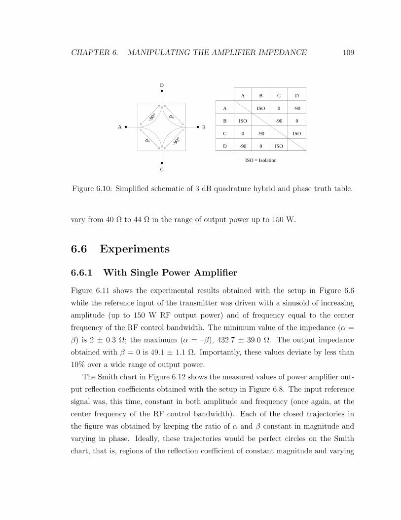
CHAPTER 6. MANIPULATING THE AMPLIFIER IMPEDANCE 109
-90°
-90°0°
0°
A
D
C
B
A
ISO
0
-90
B
ISO
-90
0
C
0
-90
ISO
D
-90
0
ISO
A
B
C
D
ISO = Isolation
Figure 6.10: Simplified schematic of 3 dB quadrature hybrid and phase truth table.
vary from 40 Ω to 44 Ω in the range of output power up to 150 W.
6.6 Experiments
6.6.1 With Single Power Amplifier
Figure 6.11 shows the experimental results obtained with the setup in Figure 6.6
while the reference input of the transmitter was driven with a sinusoid of increasing
amplitude (up to 150 W RF output power) and of frequency equal to the center
frequency of the RF control bandwidth. The minimum value of the impedance (α =
β) is 2 ± 0.3 Ω; the maximum (α = –β), 432.7 ± 39.0 Ω. The output impedance
obtained with β = 0 is 49.1 ± 1.1 Ω. Importantly, these values deviate by less than
10% over a wide range of output power.
The Smith chart in Figure 6.12 shows the measured values of power amplifier out-
put reflection coefficients obtained with the setup in Figure 6.8. The input reference
signal was, this time, constant in both amplitude and frequency (once again, at the
center frequency of the RF control bandwidth). Each of the closed trajectories in
the figure was obtained by keeping the ratio of α and β constant in magnitude and
varying in phase. Ideally, these trajectories would be perfect circles on the Smith
chart, that is, regions of the reflection coefficient of constant magnitude and varying
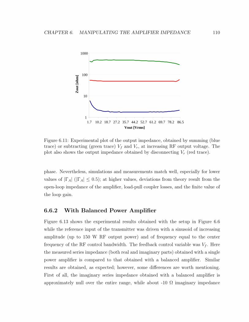
CHAPTER 6. MANIPULATING THE AMPLIFIER IMPEDANCE 110
1
10
100
1000
1.7 10.2 18.7 27.2 35.7 44.2 52.7 61.2 69.7 78.2Vout [Vrms]
Zou
t [oh
m]
86.5
Figure 6.11: Experimental plot of the output impedance, obtained by summing (bluetrace) or subtracting (green trace) Vf and Vr, at increasing RF output voltage. Theplot also shows the output impedance obtained by disconnecting Vr (red trace).
phase. Nevertheless, simulations and measurements match well, especially for lower
values of |ΓA| (|ΓA| ≤ 0.5); at higher values, deviations from theory result from the
open-loop impedance of the amplifier, load-pull coupler losses, and the finite value of
the loop gain.
6.6.2 With Balanced Power Amplifier
Figure 6.13 shows the experimental results obtained with the setup in Figure 6.6
while the reference input of the transmitter was driven with a sinusoid of increasing
amplitude (up to 150 W RF output power) and of frequency equal to the center
frequency of the RF control bandwidth. The feedback control variable was Vf . Here
the measured series impedance (both real and imaginary parts) obtained with a single
power amplifier is compared to that obtained with a balanced amplifier. Similar
results are obtained, as expected; however, some differences are worth mentioning.
First of all, the imaginary series impedance obtained with a balanced amplifier is
approximately null over the entire range, while about -10 Ω imaginary impedance
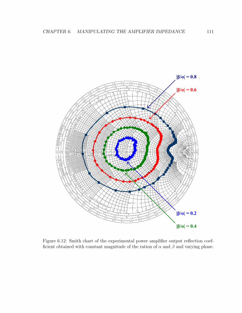
CHAPTER 6. MANIPULATING THE AMPLIFIER IMPEDANCE 111
|β/α| = 0.8
|β/α| = 0.6
|β/α| = 0.4
|β/α| = 0.2
Figure 6.12: Smith chart of the experimental power amplifier output reflection coef-ficient obtained with constant magnitude of the ration of α and β and varying phase.
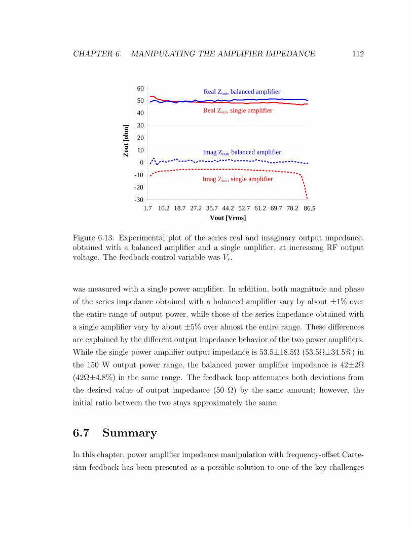
CHAPTER 6. MANIPULATING THE AMPLIFIER IMPEDANCE 112
1.7 10.2 18.7 27.2 35.7 44.2 52.7 61.2 69.7 78.2Vout [Vrms]
Zou
t [oh
m]
86.5-30
-20
-10
0
10
20
30
40
50
60
Real Zout, single amplifier
Real Zout, balanced amplifier
Imag Zout, single amplifier
Imag Zout, balanced amplifier
Figure 6.13: Experimental plot of the series real and imaginary output impedance,obtained with a balanced amplifier and a single amplifier, at increasing RF outputvoltage. The feedback control variable was Vr.
was measured with a single power amplifier. In addition, both magnitude and phase
of the series impedance obtained with a balanced amplifier vary by about ±1% over
the entire range of output power, while those of the series impedance obtained with
a single amplifier vary by about ±5% over almost the entire range. These differences
are explained by the different output impedance behavior of the two power amplifiers.
While the single power amplifier output impedance is 53.5±18.5Ω (53.5Ω±34.5%) in
the 150 W output power range, the balanced power amplifier impedance is 42±2Ω
(42Ω±4.8%) in the same range. The feedback loop attenuates both deviations from
the desired value of output impedance (50 Ω) by the same amount; however, the
initial ratio between the two stays approximately the same.
6.7 Summary
In this chapter, power amplifier impedance manipulation with frequency-offset Carte-
sian feedback has been presented as a possible solution to one of the key challenges

CHAPTER 6. MANIPULATING THE AMPLIFIER IMPEDANCE 113
faced by designers of MRI transmitter arrays, namely, the problem of coupling be-
tween coil elements.
The setup and results of experiments conducted with both single and balanced
power amplifiers have been shown and demonstrate that the output reflection coef-
ficient of these amplifiers can be manipulated to obtain almost any value within a
large area of the Smith chart, and is stable over the power range.
In principle, since Zout is tunable, any length of coaxial cable can be used between
the power amplifier and transmit coil and the system can be used with a variety of
different amplifier and coil designs.
Chapter 7
Conclusion
The research in this dissertation grew from the study of different methods and tech-
nologies, and from their successful integration and application to the field of MRI.
Petrovic’s publications on Cartesian feedback (1984), Marshall’s patent of active
polyphase amplifiers (1986), Kurpad’s work on increasing the impedance of power
amplifiers for arrays of MRI coils (2006), and several other concepts and resources
were merged and applied in this research work, which led to the original solution to
the problems of MRI RF transmit power generation described in this dissertation.
The main lesson that I have learned through my research is that we tend to
approach the science of MRI from a very limited angle, looking for knowledge and
inspiration within the community of scientists to which we belong. The result is that
“new” technologies are invented 20 years after they were first proposed in a different
field. Opportunities to accelerate growth are missed. Conversely, great ideas and
advancements are confined and do not reach the potential they truly deserve. We
should stop looking at scientific fields as “compartments,” and be open to discussing
problems and resources outside our comfort zone. The new kinds of solutions that
can be created with this approach will benefit everyone.
MRI RF systems are quickly reaching a level of complexity that calls for a deeper
relationship between this field and the field of communications. As the MRI frequency
and bandwidth increases, the overlap with the operating frequency of current radio
systems and devices increases. As MRI transmitter array systems gain acceptance,
114
CHAPTER 7. CONCLUSION 115
the use of multiple antennas at both the transmitter and receiver will also contribute
to attenuating the differences between the two fields.
Obviously, some elements will certainly remain to differentiate MRI from commu-
nications substantially. While the concepts and ideas can be translated from one field
to another, the requirements of their particular implementation will perhaps always
be very different. The frequency-offset Cartesian feedback system presented in this
dissertation would look profoundly different in a smart phone.
This is a very exciting time to be working in MRI. There is a lot of work to be done
to make the MRI RF systems more linear, more efficient, safer, and faster. The same
architecture presented in this dissertation offers many opportunities for continuous
advancement and further investigation:
• Efficiency boosting methods, such as the Doherty technique, could be applied
with frequency-offset Cartesian feedback to lower the RF dissipation in MRI.
• Digital predistortion could be also merged with the present solution, to develop
the frequency-offset variation of the two-point architecture described by [16].
• Different compensation methods could be explored that will relax the require-
ments for stability and allow one to obtain higher modulation bandwidths. (For
example, polyphase loop error amplifiers with lead-lag compensation can be im-
plemented.)
• A frequency-offset Cartesian feedback with tunable center frequency of the con-
trol bandwidth could be obtained using voltage-controlled digital resistors (in
a discrete design) or switched-capacitors (in an analog design) in place of the
fixed-value crossing resistors that couple the quadrature signals in the polyphase
architecture. This architecture would make frequency-hopping for multi-slice
applications possible, simply by tuning the center frequency of the polyphase
amplifier’s complex IF bandwidth.
• Similarly, a tunable-RF-frequency Cartesian feedback based on polyphase am-
plifiers could be demonstrated by using a voltage-controlled oscillator (VCO) or
CHAPTER 7. CONCLUSION 116
direct digital synthesizer (DDS) in place of the fixed local oscillator currently im-
plemented in the Cartesian transmitter. The system would thus be adaptable to
image multiple nuclei, such as carbon-13 (gyromagnetic ratio 10.71 MHz/T) and
phosphorus-31(gyromagnetic ratio 17.25 MHz/T), at different field strengths .
• A re-designed Cartesian feedback transmitter could be useful that integrates on-
board the main discrete components of the system. For example, two on-board
vector modulators could be obtained using two feedback signal inputs, two vari-
able gain feedback amplifiers, and two phase shifters (one for each path). Also,
better matching of the chip’s input/output dynamic range to the typical MRI
power amplifier’s range would be desirable, to eliminate the need for significant
attenuation in the feedback path that currently makes the system susceptible
to the noise generated by the down-mixer.
We are in the middle of a revolution in new kinds of MRI RF systems to solve
some of the crucial problems that limit the applicability of the most recent MRI
technologies. I feel that frequency-offset Cartesian feedback methods are an oppor-
tunity to deal with these problems successfully and I look forward to seeing what the
beginnings described in this dissertation will set in motion.
Appendix A
Active Cable Trap
A.1 Introduction
This appendix presents the “active cable trap” concept and prototype for attenuation
of the currents induced in interventional devices. It is, in essence, a miniaturized and
simplified version of the frequency-offset Cartesian feedback for MRI power amplifiers
described in this dissertation.
The idea and prototyping of the active cable trap actually preceded in time the
development of the frequency-offset Cartesian feedback system, and served as a learn-
ing tool that inspired much of the design choices regarding the latter (in particular,
the auto-calibration setup).
The active cable trap concept was invented to deal with the problem of induced
RF currents in interventional devices by the RF fields of MRI. At the sharp end of
the device, if the conditions for resonance are established, the local electric field is
high and can induce currents in a body in its close vicinity. These currents can, in
turn, create significant heating and thus burns.
In this appendix, the theory and previous work on RF-induced currents and heat-
ing in interventional devices is revisited. The architecture of the active cable trap is
then discussed. Finally, the results of experiments on looped wire current attenuation
are presented.
117
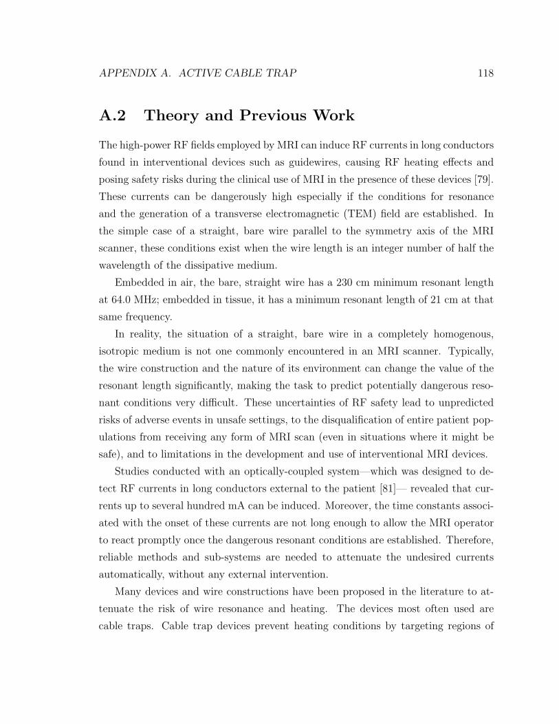
APPENDIX A. ACTIVE CABLE TRAP 118
A.2 Theory and Previous Work
The high-power RF fields employed by MRI can induce RF currents in long conductors
found in interventional devices such as guidewires, causing RF heating effects and
posing safety risks during the clinical use of MRI in the presence of these devices [79].
These currents can be dangerously high especially if the conditions for resonance
and the generation of a transverse electromagnetic (TEM) field are established. In
the simple case of a straight, bare wire parallel to the symmetry axis of the MRI
scanner, these conditions exist when the wire length is an integer number of half the
wavelength of the dissipative medium.
Embedded in air, the bare, straight wire has a 230 cm minimum resonant length
at 64.0 MHz; embedded in tissue, it has a minimum resonant length of 21 cm at that
same frequency.
In reality, the situation of a straight, bare wire in a completely homogenous,
isotropic medium is not one commonly encountered in an MRI scanner. Typically,
the wire construction and the nature of its environment can change the value of the
resonant length significantly, making the task to predict potentially dangerous reso-
nant conditions very difficult. These uncertainties of RF safety lead to unpredicted
risks of adverse events in unsafe settings, to the disqualification of entire patient pop-
ulations from receiving any form of MRI scan (even in situations where it might be
safe), and to limitations in the development and use of interventional MRI devices.
Studies conducted with an optically-coupled system—which was designed to de-
tect RF currents in long conductors external to the patient [81]— revealed that cur-
rents up to several hundred mA can be induced. Moreover, the time constants associ-
ated with the onset of these currents are not long enough to allow the MRI operator
to react promptly once the dangerous resonant conditions are established. Therefore,
reliable methods and sub-systems are needed to attenuate the undesired currents
automatically, without any external intervention.
Many devices and wire constructions have been proposed in the literature to at-
tenuate the risk of wire resonance and heating. The devices most often used are
cable traps. Cable trap devices prevent heating conditions by targeting regions of
APPENDIX A. ACTIVE CABLE TRAP 119
high RF current, where energy storage is inductive. Toroidal cable traps inductively
couple a high resistance in series with the wire to spoil the resonant Q or modify the
resonant frequency of the wire. Here, the wire itself acts as the primary coil, and a
resonant toroidal cavity enfolding the wire acts as the secondary coil. In 2000, Ladd
and Quick [50] added coaxial chokes with length λ4
to coaxial cables in order to reduce
the amplitude of the MRI-induced currents on the cable shields. In 2005, Hillenbrand
[30] described the “bazooka coil,” a balun-style RF trap, and demonstrated its ca-
pability to reduce the formation of resonating RF waves on long conductors during
transmission. Hillenbrand also interfaced the cable trap to a preamplifier circuit, used
in this case as a dual-mode receiver.
As an alternative to cable traps, the use of lossy dielectrics (also called Q-spoilers)
has been proposed [79]. The principle of these devices is that of coupling of the
free-end of a wire–where the E field is maximum and energy storage is primarily
capacitive—with a lossy dielectric: by inserting the wire into the dielectric, the quality
factor of the resonant wire is reduced, thereby reducing the dangerous resonant effects.
All of the above are passive methods and thus share one important limitation,
that is, their ability to attenuate wire currents is significantly restricted by component
loss and tuning interactions. In experiments with the optically-coupled monitoring
system, it was demonstrated that a Q-spoiling lossy dielectric reduces the RF power
of a resonant guidewire current to 14% of its value in the free wire, and a properly
tuned balun-style RF trap reduces it to 23%; however, variations in the guidewire
environment or in the devices inevitably changed the resonant characteristics and
can drastically impact these outcomes.
A.3 Feedback Method for Current Attenuation
A potential solution to the problem of RF heating in guidewires is to create an auto-
matic negative feedback control system to sense and attenuate the RF wire current. A
device capable of doing so is a much simplified version of the frequency-offset Carte-
sian feedback system described in the previous chapters: equipped with the same
current sensor used in the optically-coupled monitoring system, the system would, in
APPENDIX A. ACTIVE CABLE TRAP 120
Sensor
LO
Actuator
QUADRATUREUPMIXER
OPENLOOP
CLOSEDLOOP
WIRE
TEST
RF‐INDUCED CURRENT
/2 p
hase
sp
litte
r
QUADRATURE DOWNMIXER
LO
balun balun
/2 p
hase
sp
litte
r
Vcm
Vcm
Sensor
LO
Actuator
AD5385UP-MIXER
WIRERF-INDUCED CURRENT
AD8348DOWN-MIXER
LO
balun balun
phase splitter
phase splitter
POLYPHASE AMPLIFIERS
Figure A.1: Simplified schematic of active cable trap. The feedback loop input isthe RF current flowing in a potentially dangerous conductor, which is detected bya toroidal sensor. After down-conversion, the loop compares the detected signal toa DC reference, and amplifies the difference by the polyphase amplifier gain. Afterup-conversion, the amplified error signal drives a toroidal actuator that induces inthe conductor itself an RF current that opposes the one induced by the B1 field.
theory, offer a wire current attenuation equal to the system loop gain over a range
of frequencies designed to match the known bandwidth of RF excitation. To test
these ideas, a miniaturized version of the frequency-offset Cartesian feedback system,
acting as an “active cable trap,” was designed.
Figure A.1 shows a simplified schematic of the active cable trap. The feedback
loop input of the active cable trap is the RF current flowing in a potentially dangerous
conductor, which is detected by a toroidal sensor. After down-conversion, the loop
compares the detected signal to a DC reference, and amplifies the difference (i.e.,
the error signal) by the polyphase amplifier gain H(ω). After up-conversion, the
amplified error signal drives a toroidal actuator that induces in the conductor itself
an RF current that opposes the one induced by the B1 field. As in the frequency-
offset Cartesian control system for MRI power amplifiers, the active cable trap uses a
Cartesian down/up-conversion scheme, so that amplification is obtained at a low-IF
APPENDIX A. ACTIVE CABLE TRAP 121
band, where values of loop gain up to 100 (40 dB) and bandwidth of hundreds of
kHz can be obtained; in addition, the polyphase loop error amplifiers eliminate the
possibility of quadrature errors caused by phase and amplitude mismatches, which
in this application could lead to the generation of an “image” or quadrature ghost
excitation by the wire.
As previously discussed, the ability of the control loop to preserve the phase in-
tegrity of the signal is crucial to the stability of the loop. While in the MRI power
amplifier system, phase alignment is obtained with the shift control circuitry inte-
grated in the CMX998 IC, with the active cable trap the phase alignment is obtained
by phase-locking two external signals providing the LO frequencies to the demodula-
tor and modulator, respectively.
The architecture of the active cable trap can be conceptually divided into five
separate elements: a toroidal sensor, a quadrature demodulator, the polyphase loop
error amplifiers, a quadrature modulator, and a toroidal actuator. These elements
are discussed in detail below.
A.3.1 Toroidal Sensor
.
The long conductor, whose RF current must be monitored and reduced, is fed
through a toroid-cavity sensor shown in Figure A.2. The toroid-cavity acts as a
volume-rotated rectangular single-turn transformer secondary and can be thought of
as a self-shielded pick-up loop. It consists of copper tape wrapped around a toroidal
Teflon core with 1.55 mm inner diameter and 5.50 mm outer diameter. Any long
conductor fed through the core of the toroid-cavity acts as the transformer primary.
MRI-induced currents on the wire will couple a magnetic flux to the toroid secondary
given by
Φ = µ0
ln ba
2πg · I = M · I (A.1)
where a, b are the inner and outer radius of the toroid, respectively; g is the length of
the toroidal cavity; I is the wire current, and M is the mutual inductance. Faraday’s
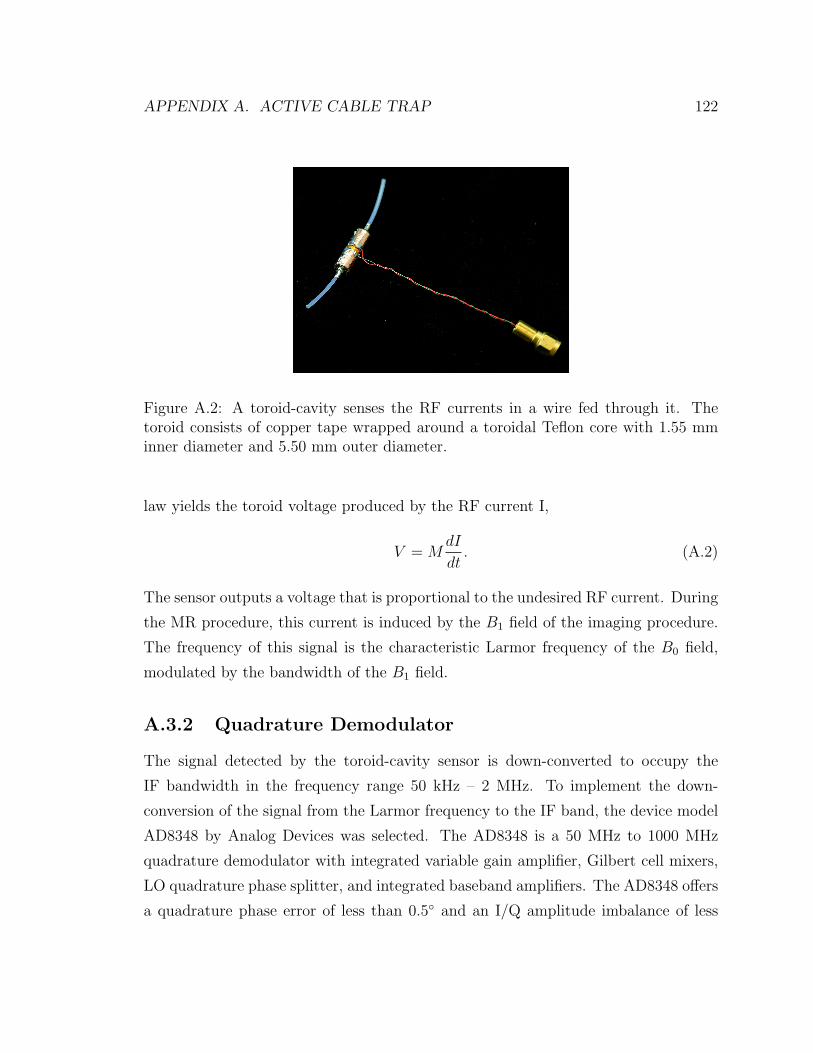
APPENDIX A. ACTIVE CABLE TRAP 122
Figure A.2: A toroid-cavity senses the RF currents in a wire fed through it. Thetoroid consists of copper tape wrapped around a toroidal Teflon core with 1.55 mminner diameter and 5.50 mm outer diameter.
law yields the toroid voltage produced by the RF current I,
V = MdI
dt. (A.2)
The sensor outputs a voltage that is proportional to the undesired RF current. During
the MR procedure, this current is induced by the B1 field of the imaging procedure.
The frequency of this signal is the characteristic Larmor frequency of the B0 field,
modulated by the bandwidth of the B1 field.
A.3.2 Quadrature Demodulator
The signal detected by the toroid-cavity sensor is down-converted to occupy the
IF bandwidth in the frequency range 50 kHz – 2 MHz. To implement the down-
conversion of the signal from the Larmor frequency to the IF band, the device model
AD8348 by Analog Devices was selected. The AD8348 is a 50 MHz to 1000 MHz
quadrature demodulator with integrated variable gain amplifier, Gilbert cell mixers,
LO quadrature phase splitter, and integrated baseband amplifiers. The AD8348 offers
a quadrature phase error of less than 0.5 and an I/Q amplitude imbalance of less
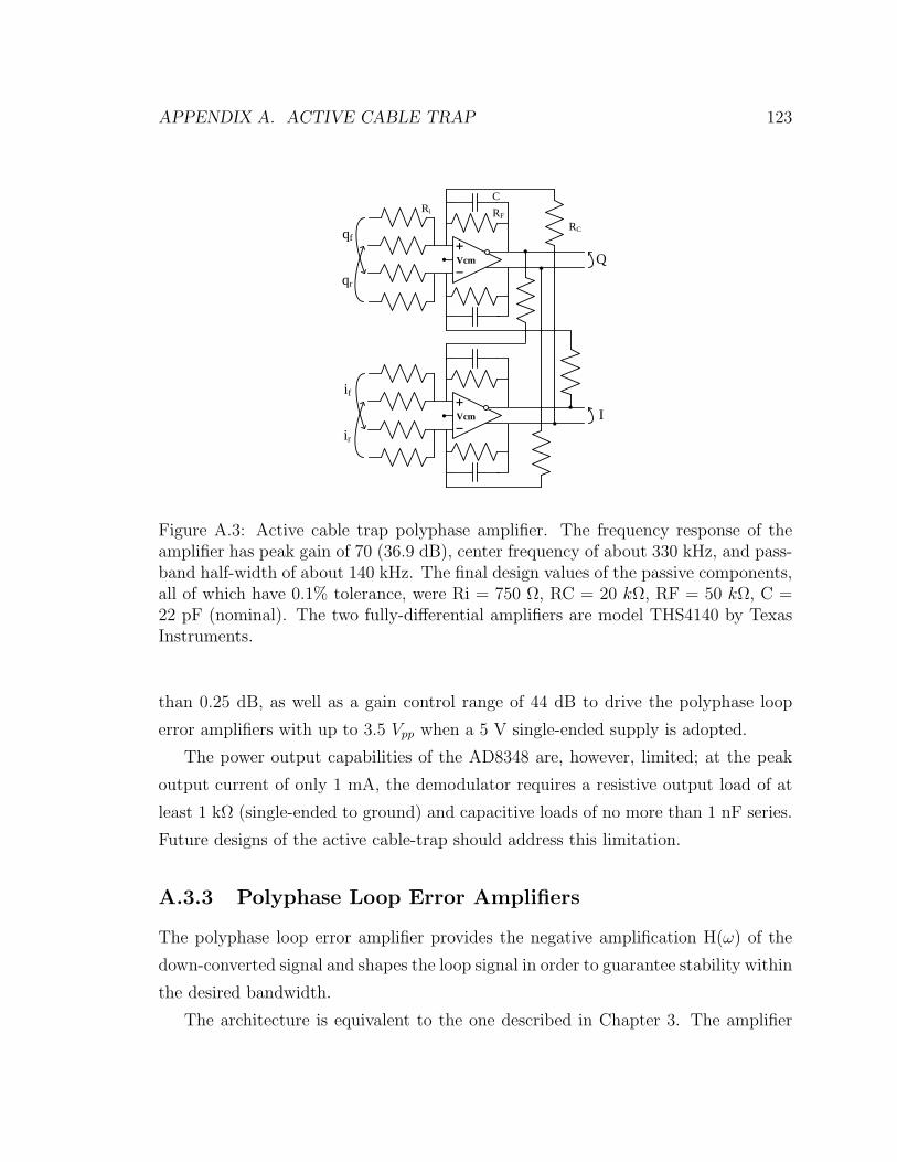
APPENDIX A. ACTIVE CABLE TRAP 123
Vcm
Vcm
ir
Q
I
if
qr
qf
Ri RF
C
RC
+
−
+
−
Figure A.3: Active cable trap polyphase amplifier. The frequency response of theamplifier has peak gain of 70 (36.9 dB), center frequency of about 330 kHz, and pass-band half-width of about 140 kHz. The final design values of the passive components,all of which have 0.1% tolerance, were Ri = 750 Ω, RC = 20 kΩ, RF = 50 kΩ, C =22 pF (nominal). The two fully-differential amplifiers are model THS4140 by TexasInstruments.
than 0.25 dB, as well as a gain control range of 44 dB to drive the polyphase loop
error amplifiers with up to 3.5 Vpp when a 5 V single-ended supply is adopted.
The power output capabilities of the AD8348 are, however, limited; at the peak
output current of only 1 mA, the demodulator requires a resistive output load of at
least 1 kΩ (single-ended to ground) and capacitive loads of no more than 1 nF series.
Future designs of the active cable-trap should address this limitation.
A.3.3 Polyphase Loop Error Amplifiers
The polyphase loop error amplifier provides the negative amplification H(ω) of the
down-converted signal and shapes the loop signal in order to guarantee stability within
the desired bandwidth.
The architecture is equivalent to the one described in Chapter 3. The amplifier
APPENDIX A. ACTIVE CABLE TRAP 124
is realized with two cross-connected fully-differential amplifiers (model THS4140 by
Texas instruments). Each amplifier, arranged in a single-supply fully differential
configuration, is DC-coupled to the demodulator’s differential output.
The passive components in the loop error amplifiers, whose values are described in
Figure A.3, have 0.1% tolerance to guarantee 60 dB sideband rejection to quadrature
mismatches created by the AD8348.
A.3.4 Quadrature Modulator
The output of the polyphase loop error amplifiers drives a quadrature modulator
(model AD5385 50 MHz to 2200 MHz by Analog Devices). At the output frequency
of 65 MHz, the AD5385 offers a quadrature phase error of 0.17 degrees only and a
very low quadrature amplitude imbalance of 0.03 dB.
As in the AD8348, the power output capabilities of the AD5385 are modest (a
maximum power of 8 dBm can be delivered), which makes it possible to induce
wire currents of only about 10 mARMS using the toroidal actuator. While adequate
for testing the proposed application on the bench, future designs should consider
replacing the AD5385 or the toroidal actuator with devices that offer higher output
capabilities. This will allow the active cable trap to work with much higher wire
currents. The AD5385 is powered by a 5V single supply, as is the AD8348.
A.3.5 Toroidal actuator
The toroidal actuator is an exact replica of the toroidal sensor. Driven by the AD5385
modulator output signal, the actuator operates on the long conductor. When the
feedback loop is closed and stable, the toroidal actuator induces in the conductor a
current which is, ideally, the negated and amplified version of the current originally
caused by interactions with the B1 field. The net result is that a substantially smaller
current, inversely proportional to the value of the loop gain, is present on the wire.
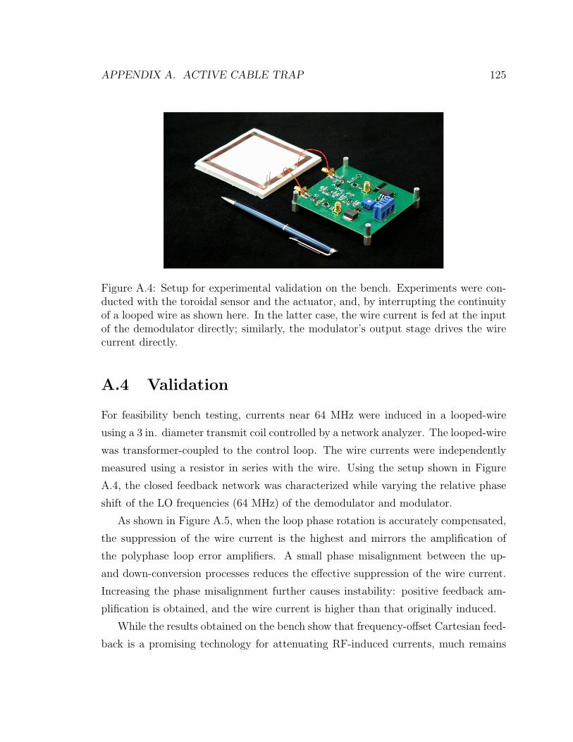
APPENDIX A. ACTIVE CABLE TRAP 125
Figure A.4: Setup for experimental validation on the bench. Experiments were con-ducted with the toroidal sensor and the actuator, and, by interrupting the continuityof a looped wire as shown here. In the latter case, the wire current is fed at the inputof the demodulator directly; similarly, the modulator’s output stage drives the wirecurrent directly.
A.4 Validation
For feasibility bench testing, currents near 64 MHz were induced in a looped-wire
using a 3 in. diameter transmit coil controlled by a network analyzer. The looped-wire
was transformer-coupled to the control loop. The wire currents were independently
measured using a resistor in series with the wire. Using the setup shown in Figure
A.4, the closed feedback network was characterized while varying the relative phase
shift of the LO frequencies (64 MHz) of the demodulator and modulator.
As shown in Figure A.5, when the loop phase rotation is accurately compensated,
the suppression of the wire current is the highest and mirrors the amplification of
the polyphase loop error amplifiers. A small phase misalignment between the up-
and down-conversion processes reduces the effective suppression of the wire current.
Increasing the phase misalignment further causes instability: positive feedback am-
plification is obtained, and the wire current is higher than that originally induced.
While the results obtained on the bench show that frequency-offset Cartesian feed-
back is a promising technology for attenuating RF-induced currents, much remains
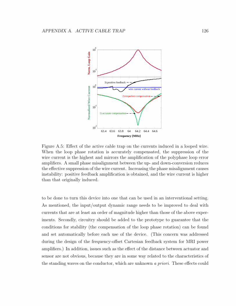
APPENDIX A. ACTIVE CABLE TRAP 126
63.4 63.6 63.8 64 64.2 64.4 64.6
10-1
100
63.4 63.6 63.8 64 64.2 64.4 64.610
-2
10-1
100
Frequency [MHz]
Nor
m. L
oop
Gai
nN
orm
aliz
ed W
ire
Cur
rent
1) accurate compensation
2) imperfect compensation
3) positive feedback
wire current without feedback
Figure A.5: Effect of the active cable trap on the currents induced in a looped wire.When the loop phase rotation is accurately compensated, the suppression of thewire current is the highest and mirrors the amplification of the polyphase loop erroramplifiers. A small phase misalignment between the up- and down-conversion reducesthe effective suppression of the wire current. Increasing the phase misalignment causesinstability: positive feedback amplification is obtained, and the wire current is higherthan that originally induced.
to be done to turn this device into one that can be used in an interventional setting.
As mentioned, the input/output dynamic range needs to be improved to deal with
currents that are at least an order of magnitude higher than those of the above exper-
iments. Secondly, circuitry should be added to the prototype to guarantee that the
conditions for stability (the compensation of the loop phase rotation) can be found
and set automatically before each use of the device. (This concern was addressed
during the design of the frequency-offset Cartesian feedback system for MRI power
amplifiers.) In addition, issues such as the effect of the distance between actuator and
sensor are not obvious, because they are in some way related to the characteristics of
the standing waves on the conductor, which are unknown a priori. These effects could

APPENDIX A. ACTIVE CABLE TRAP 127
not only ultimately hinder the effectiveness of the negative feedback attenuation, but
also change the characteristics of the loop and thus compromise its stability.

Bibliography
[1] G. Adriany, P.F. Van de Moortele, F. Wiesinger, S. Moeller, J.P. Strupp, P. An-
dersen, C. Snyder, X. Zhang, W. Chen, and K.P. Pruessmann. Transmit and
receive transmission line arrays for 7 Tesla parallel imaging. Magnetic Resonance
in Medicine, 53(2):434–445, 2005.
[2] E. Aschbacher and M. Rupp. Modelling and identification of a nonlinear power-
amplifier with memory for nonlinear digital adaptive pre-distortion. In Proceed-
ings of 4th IEEE Workshop Signal Processing Advances Wireless Communica-
tions, pages 658–662, 2003.
[3] F. Behbahani, Y. Kishigami, J. Leete, and A.A. Abidi. CMOS mixers and
polyphase filters for large image rejection. IEEE Journal of Solid-State Circuits,
36(6):873–887, 2001.
[4] M. Boloorian and J.P. McGeehan. Linearisation of frequency-hopped transmit-
ters using Cartesian feedback. Proceedings of the 45th IEEE Vehicular Technology
Conference, 2:520–524, 1995.
[5] M. Boloorian and JP McGeehan. The frequency-hopped Cartesian feedback
linear transmitter. IEEE Transactions on Vehicular Technology, 45(4):688–706,
1996.
[6] M. Boloorian and J.P. McGeehan. Maximization of Cartesian transmitter lin-
earisation bandwidth. Electronics Letters, 32(19):1823–1824, 1996.
[7] M. Boloorian and J.P. McGeehan. Phase-lag compensated Cartesian feedback
transmitter. Electronics Letters, 32(17):1547–1548, 1996.
128
BIBLIOGRAPHY 129
[8] M. Boloorian and J.P. McGeehan. Twin-loop Cartesian transmitter. Electronics
Letters, 32(11):971–972, 1996.
[9] M.A. Briffa and M. Faulkner. Dynamically biased Cartesian feedback lineariza-
tion. Proceedings of the 43rd IEEE Vehicular Technology Conference, pages 672–
675, 1993.
[10] M.A. Briffa and M. Faulkner. Gain and phase margins of Cartesian feedback
RF amplifier linearization. Journal of Electrical and Electronics Engineering
Australia, 14:283–283, 1994.
[11] M.A. Briffa and M. Faulkner. Stability considerations for dynamically biased
Cartesian feedback linearization. Proceedings of the 44th IEEE Vehicular Tech-
nology Conference, 2:1321–1325, Jun 1994.
[12] M.A. Briffa and M. Faulkner. Stability analysis of Cartesian feedback lineariza-
tion for amplifiers with weak nonlinearities. Proceedings of IEE Communications,
143(4):212–218, 1996.
[13] W.B. Bruene. Antenna tuner discriminator, 1985. US Patent 4,493,112.
[14] C.Y. Chou and C.Y. Wu. The design of wideband and low-power CMOS active
polyphase filter and its application in RF double-quadrature receivers. IEEE
Transactions on Circuits and Systems I: Regular Papers, 52(5):825–833, 2005.
[15] X. Chu, X. Yang, Y. Liu, J. Sabate, and Y. Zhu. Ultra-low output impedance
RF power amplifier for parallel excitation. Magnetic Resonance in Medicine,
61(4):952–61, 2009.
[16] S. Chung, J.W. Holloway, and J. Dawson. Energy-efficient digital predistortion
with lookup table training using analog Cartesian feedback. IEEE Transactions
on Microwave Theory and Techniques, 56(10):2248–2258, 2008.
BIBLIOGRAPHY 130
[17] C.M. Collins, W. Liu, B.J. Swift, and M.B. Smith. Combination of optimized
transmit arrays and some receive array reconstruction methods can yield ho-
mogeneous images at very high frequencies. Magnetic Resonance in Medicine,
54(6):1327–1332, 2005.
[18] J. Crols and M.S.J. Stayeart. An analog integrated polyphase filter for a high
performance low-IF receiver. 1995 IEEE Symposium on VLSl Circuits: Digest
of Technical Papers, pages 87–88, 1995.
[19] J. Crols and M.S.J. Steyaert. Low-IF topologies for high-performance analog
front ends of fully integrated receivers. IEEE Transactions on Circuits and Sys-
tems II: Analog and Digital Signal Processing, 45(3):269–282, 1998.
[20] J.L. Dawson and T.H. Lee. Automatic phase alignment for a fully integrated
Cartesian feedback power amplifier system. IEEE Journal of Solid-State Circuits,
38(12):2269–2279, 2003.
[21] J.P. De Wilde, D. Grainger, D.L. Price, and C. Renaud. Magnetic resonance
imaging safety issues including an analysis of recorded incidents within the UK.
Progress in Nuclear Magnetic Resonance Spectroscopy, 51(1):37–48, 2007.
[22] K. Eisele, R. Engelbrecht, and K. Kurokawa. Balanced transistor amplifiers for
precise wideband microwave applications. In 1965 IEEE International Solid-
State Circuits Conference: Digest of Technical Papers, volume 8, 1965.
[23] R.S. Engelbrecht and K. Kurokawa. A wide-band low noise L-band balanced
transistor amplifier. Proceedings of the IEEE, 53(3):237–247, 1965.
[24] M. Faulkner. Amplifier linearization using RF feedback and feedforward tech-
niques. IEEE Transactions on Vehicular Technology, 47(1):209–215, 1998.
[25] M. Faulkner, D. Contos, and M. Johansson. Linearization of power amplifiers
using RF feedback. Electronics Letters, 31(23):2023–2024, 1995.
BIBLIOGRAPHY 131
[26] R. Frayne, B.G. Goodyear, P. Dickhoff, M.L. Lauzon, and R.J. Sevick. Magnetic
resonance imaging at 3.0 Tesla: challenges and advantages in clinical neurological
imaging. Investigative radiology, 38(7):385, 2003.
[27] H. Granberg. AN-779 Application Note: Low-distortion 1.6 to 30 MHz SSB
driver design. Motorola, Inc, 1977.
[28] H. Granberg. AN-313 Application Note: Wideband RF power amplifier. Mo-
torola, Inc., 1988.
[29] P.R. Gray, P.J. Hurst, S.H. Lewis, and R.G. Meyer. Analysis and design of analog
integrated circuits. Wiley India Pvt. Ltd., 2008.
[30] C.M. Hillenbrand, D.R. Elgort, E.Y. Wong, A. Reykowski, F.K. Wacker, J.S.
Lewin, and J.L. Duerk. Active device tracking and high-resolution intravascular
MRI using a novel catheter-based, opposed-solenoid phased array coil. Magnetic
Resonance in Medicine, 51(4):668–675, 2004.
[31] D.I. Hoult, D. Foreman, G. Kolansky, and D. Kripiakevich. Overcoming high-
field RF problems with non-magnetic Cartesian feedback transceivers. Magnetic
Resonance Materials in Physics, Biology and Medicine, 21(1):15–29, 2007.
[32] D.I. Hoult, G. Kolansky, and D. Kripiakevich. A HI-FI Cartesian feedback spec-
trometer for precise quantitation and superior performance. Journal of Magnetic
Resonance, 171(1):57–63, 2004.
[33] D.I. Hoult, G. Kolansky, D. Kripiakevich, and S.B. King. The NMR multi-
transmit phased array: a Cartesian feedback approach. Journal of Magnetic
Resonance, 171(1):64–70, 2004.
[34] D.I. Hoult and P.C. Lauterbur. The sensitivity of the zeugmatographic experi-
ment involving human samples. Journal of Magnetic Resonance, 34(2):425–433,
1979.
[35] M. Johansson and T. Mattsson. Linearized high-efficiency power amplifier for
PCN. Electronics Letters, 27(9):762–764, 1991.
BIBLIOGRAPHY 132
[36] M. Johansson and T. Mattsson. Transmitter linearization using Cartesian feed-
back for linear TDMA modulation. 41st IEEE Vehicular Technology Conference,
pages 439–444, 1991.
[37] M. Johansson, T. Mattsson, L. Sundstrom, and M. Faulkner. Linearization
of multi-carrier power amplifiers. 43rd IEEE Vehicular Technology Conference,
pages 684–687, 1993.
[38] M. Johansson and L. Sundstrom. Linearization of RF multicarrier amplifiers
using cartesian feedback. Electronics Letters, 30(14):1110–1112, 1994.
[39] J. Kaukovuori, K. Stadius, J. Ryynanen, and KAI Halonen. Analysis and de-
sign of passive polyphase filters. IEEE Transactions on Circuits and Systems I:
Regular Papers, 55(10):3023–3037, 2008.
[40] P. Kenington. High linearity RF amplifier design. Artech House, 2000.
[41] P.B. Kenington, R.J. Wilkinson, and K.J. Parsons. Noise performance of a Carte-
sian loop transmitter. IEEE Transactions on Vehicular Technology, 46(2):467–
476, 1997.
[42] R. King, C. Harrison Jr, and D. Tingley. The admittance of bare circular loop
antennas in a dissipative medium. IEEE Transactions on Antennas and Propa-
gation, 12(4):434–438, 1964.
[43] R.W.P. King. The linear antenna: Eighty years of progress. Proceedings of the
IEEE, 55(1):2–16, 1967.
[44] R.W.P. King. The many faces of the insulated antenna. Proceedings of the IEEE,
64(2):228–238, 1976.
[45] M.K. Konings, L.W. Bartels, H.F. Smits, and C.J. Bakker. Heating around
intravascular guidewires by resonating RF waves. Journal of magnetic resonance
imaging : JMRI, 12(1):79–85, 2000.
BIBLIOGRAPHY 133
[46] H. Ku, M.D. McKinley, and J.S. Kenney. Quantifying memory effects in RF
power amplifiers. IEEE Transactions on Microwave Theory and Techniques,
50(12):2843–2849, 2002.
[47] K.N. Kurpad, E.B. Boskamp, and S.M. Wright. Implementation of coil integrated
RF power MOSFET as voltage controlled current source in a transmit phased
array coil. In International Society of Magnetic Resonance in Medicine 12th,
volume 1585, 2004.
[48] K.N. Kurpad, S.M. Wright, and E.B. Boskamp. RF current element design
for independent control of current amplitude and phase in transmit phased ar-
rays. Magnetic Resonance Engineering: Concepts in Magnetic Resonance Part
B, 29(2):75, 2006.
[49] M.E. Ladd. High-field-strength magnetic resonance: Potential and limits. Topics
in Magnetic Resonance Imaging, 18(2):139, 2007.
[50] M.E. Ladd and H.H. Quick. Reduction of resonant RF heating in intravascular
catheters using coaxial chokes. Magnetic Resonance in Medicine, 43(4):615–619,
2000.
[51] J.M.P. Langlois, D. Al-Khalili, and R.J. Inkol. Polyphase filter approach for
high performance, FPGA-based quadrature demodulation. The Journal of VLSI
Signal Processing, 32(3):237–254, 2002.
[52] R.F. Lee, R.O. Giaquinto, and C.J. Hardy. Coupling and decoupling theory
and its application to the MRI phased array. Magnetic Resonance in Medicine,
48(1):203–213, 2002.
[53] K. Linggajaya and J.G.Y.K. Seng. A new active polyphase filter for wideband
image reject downconverter. Proceedings of the IEEE International Conference
on Semiconductor Electronics, pages 213–217, 2002.
[54] W. Mao, M.B. Smith, and C.M. Collins. Exploring the limits of RF shimming for
high-field MRI of the human head. Magnetic Resonance in Medicine, 56(4):918–
922, 2006.

BIBLIOGRAPHY 134
[55] C.B. Marshall. Active polyphase filters, February 2 1988. US Patent 4,723,318.
[56] R.D. Middlebrook. Measurement of loop gain in feedback systems. International
Journal of Electronics, 38(4):485–512, 1975.
[57] R.D. Middlebrook. Input filter considerations in design and application of switch-
ing regulators. In IEEE IAS Annual Meeting, pages 366–382. Chicago, 1976.
[58] R.D. Middlebrook. Design techniques for preventing input-filter oscillations in
switched-mode regulators. In Proceedings of POWERCON, volume 5, 1978.
[59] D.G. Norris. High field human imaging. Journal of Magnetic Resonance Imaging,
18(5), 2003.
[60] M. Notten, H. Brekelmans, and V. Rambeau. A 5th order 14 mWatt active
polyphase filter for analog and digital TV on mobile applications. Proceedings
of the 32nd European Solid-State Circuits Conference, pages 211–214, 2006.
[61] S.M. Park, R. Kamondetdacha, A. Amjad, and J.A. Nyenhuis. MRI safety: RF-
induced heating near straight wires. Digests of the IEEE International Magnetics
Conference, pages 1243–1244, 2005.
[62] J. Pauly. Parameter relations for the Shinnar-Le Roux selective excitation pulse
design algorithm. IEEE Transactions on Medical Imaging, 10(1):53–65, 1991.
[63] V. Petrovic. VHF SSB transmitter employing Cartesian feedback. IEE Confer-
ence on Telecommunications, Radio and Information Technology, pages 161–165,
1984.
[64] K.P. Pruessmann. Parallel imaging at high field strength: synergies and joint
potential. Topics in Magnetic Resonance Imaging, 15(4):237, 2004.
[65] P.B. Roemer, W.A. Edelstein, C.E. Hayes, S.P. Souza, and O.M. Mueller. The
NMR phased array. Magnetic Resonance in Medicine, 16(2):192–225, 1990.
[66] F. Schick. Whole-body MRI at high field: technical limits and clinical potential.
European Radiology, 15(5):946–959, 2005.
BIBLIOGRAPHY 135
[67] T. Schirmer, J. RA, RE Hurd, N. Sailasuta, J. Tropp, and P. Le Roux. Chemical
shift error and artifact reduction in csi using very selective saturation pulses. In
Proceedings ISMRM, 1998.
[68] G. Scott, S.S. Conolly, and A. Macovski. Polyphase techniques for low cost MRI
receivers. In Proceedings of the International Society for Magnetic Resonance in
Medicine 6th, 1998.
[69] G. Scott, P. Stang, and A. Kerr. A load pull/hot S22 analyzer for transmit array
amplifiers. In Proceedings of the International Society for Magnetic Resonance
in Medicine 17th, 2009.
[70] G. Scott, P. Stang, A. Kerr, and J. Pauly. General signal vector decoupling
for transmit arrays. In Proceedings of the International Society for Magnetic
Resonance in Medicine 16th, 2008.
[71] G. Scott, P. Stang, W. Overall, A. Kerr, and J. Pauly. A vector modulation
transmit array system. In Proceedings of the International Society for Magnetic
Resonance in Medicine 14th, 2006.
[72] F. Seifert, G. Wubbeler, S. Junge, B. Ittermann, and H. Rinneberg. Patient
safety concept for multichannel transmit coils. Journal of Magnetic Resonance
Imaging, 26(5):1315–1321, 2007.
[73] P. Stang, S. Conolly, J Pauly, and G Scott. Medusa: A scalable MR console
for parallel imaging. In Proceedings of the International Society for Magnetic
Resonance in Medicine 15th, 2007.
[74] P.P. Stang, A. Kerr, W. Grisson, J.M. Pauly, and G.C. Scott. Vector iteration
predistortion: an auto-calibration method for transmit arrays. In Proceedings of
the International Society for Magnetic Resonance in Medicine 17th, 2009.
[75] F. Tillman and H. Sjoland. A polyphase filter based on CMOS inverters. Analog
Integrated Circuits and Signal Processing, 50(1):7–12, 2007.
BIBLIOGRAPHY 136
[76] H.C. Torrey. Bloch equations with diffusion terms. Physical Review, 104(3):563–
565, 1956.
[77] T.K.C. Tran, D.B. Vigneron, N. Sailasuta, J. Tropp, P. Le Roux, J. Kurhanewicz,
S. Nelson, and R. Hurd. Very selective suppression pulses for clinical MRSI
studies of brain and prostate cancer. Magnetic Resonance in Medicine, 43(1):23–
33, 2000.
[78] T. Vaughan, L. DelaBarre, C. Snyder, J. Tian, C. Akgun, D. Shrivastava, W. Liu,
C. Olson, G. Adriany, J. Strupp, et al. 9.4 T human MRI: preliminary results.
Magnetic Resonance in Medicine, 56(6), 2006.
[79] R.D. Venook, W. Overall, J. Pauly, and G.C. Scott. Reducing and monitoring
RF heating. In Proceedings of the International Society for Magnetic Resonance
in Medicine 14th, volume 14, 2006.
[80] S.W. Watkinson. Polar loop transmitter, 1986. US Patent 4,618,999.
[81] M Zanchi, R Venook, J Pauly, and G Scott. An optically-coupled system for
monitoring of MRI-induced RF currents into long conductors. IEEE Transactions
on Medical Imaging, 2010.
[82] Y. Zhu. Parallel excitation with an array of transmit coils. Magnetic Resonance
in Medicine, 51(4):775–784, 2004.