Embed Size (px)
Citation preview

VLSI POWER REDUCTIONW A T MAHESH DANANJAYA

POWER REDUCTION
• Power reduction is very important
• Can be classified into three main categories based on their
implementation and occurrence
• Device Engineering
• This refers to techniques that are implemented on the underlying
transistor that form digital circuitry. This is mostly involved with the
transistor level components.
• Circuit Engineering
• These refer to techniques that are applied to gate/logic level, which are
clusters of transistors that perform a small computation like NAND, NOR
etc.
• System Engineering
• These are referring to techniques that can be applied to macro-blocks that
are part of a big data path or micro-chip.

LOW POWER LEVERAGES
• Parallelism and Pipelined micro-architecture
• Clock Gating
• Power Gating
• Voltage Islands
• Gate Sizing
• Multi VDD
• DVFS – Dynamic Voltage Frequency Scaling
• Device Level
• Multi Threshold Devices
• Low Capacitance in device
• High k Hf based MOS

DYNAMIC POWER REDUCTION
• Dynamic power reduction is very important because,
• Clock tree consume more than 50% of dynamic power
consumption.
• Power consumed by combinational logic whose values are changing on each
clock edge
• Power consumed by flops
• Power consumed by the clock buffer tree
• Asynchronous Logic Circuits which is not driven by the global
clock, is also changing de to state changes in the flops.

CLOCK GATING
• Major dynamic power reduction technique
• Gate the clock as much as the flop is not necessary to be toggled
• Otherwise in every clock cycle flop will toggle and dissipate more power
• Local clock gating has a new enable to every flop where clock gating is
necessary
• But with complex VLSI design it is not sustainable to use local clock
gating
• We need to derive a logic for new enable with the current logic

LOCAL CLOCK GATING
• Local enable is used to gate the flop
• Enable and clock are and gated and the gated
clock is provided to the flop
• Local enable, do not have a global perception
AND
FLOP
D Q
Enable
Clock
Data IN Data Out

CLOCK GATING METHODS
• Latch Free Clock Gating
• Latch Based Clock Gating
AND
FLOP
D Q
Enable
Clock
Data IN
Data Out
Gated CLK
AND
FLOP
D QEnable
Clock
CLK
Data OutData CLK D Q
FLOP
Gated CLK

MULTI LEVEL BOOLEAN LOGIC
• Satisfiability Don’t Care (SDC)
• Design spots where certain input/ input combination to a circuit can never
occur. There may be possible causes for the SDC conditions.
• 𝒚 = 𝒂 + 𝒃 , 𝒕𝒉𝒆𝒏 𝒚 = 𝟎, 𝒂 = 𝟏, 𝒃 = ~ 𝒘𝒊𝒍𝒍 𝒏𝒆𝒗𝒆𝒓 𝒐𝒄𝒄𝒖𝒓 (𝑺𝑫𝑪)
• Observability Don’t Care (ODC)
• Design spots where local changes cannot be observed at the primary
outputs.
• 𝒚 = 𝒂 + 𝒃,𝒘𝒉𝒆𝒏 𝒂 = 𝟏, 𝒄𝒉𝒂𝒏𝒈𝒆 𝒐𝒏 𝒃 𝒊𝒔 𝒏𝒐𝒕 𝒐𝒃𝒔𝒆𝒓𝒗𝒂𝒃𝒍𝒆

NEW TRENDS OF CLOCK GATING
• Based on the multi level Boolean logic derivations
• There are two ways of clock gating to derivate new enable based on the input and output
logics.
• Stability Condition (STC)
• Stability condition is defined with the stability of the input to the flop when
upstream flop is stable, no new data or changes come to the downstream flop
• Observability Don’t Care (ODC)
• There are Situations where the output of the flop is changing or staying
constant, but that output is not used in the downstream and read only for a
certain time period of time

STABILITY CONDITION (STC)
• Stability condition is defined as stability of the input to the flop when upstream flop is
stable, no new data or changes come to the downstream flop.
• If the input to the flop is not changing with the (Stable) for a period of time, there is no
use of toggling the flop for state changes.
• In such situation input to the flop is just remain constant thus output of the flop also
stable without changing.
• Then we can stop providing clock to the flop and save more power
EN1
Upstream register
Downstream register

STABILITY CONDITION (STC)
• Before STC
• After STC
EN
CLK
CLK
EN

OBSERVABILITY DON’T CARE (ODC)
• There are Situations where the output of the flop is changing or staying
constant, but that output is not used in the downstream and read only for
a certain time period of time.
• Then toggling and state changes of the flop for entire time period is not
required.
• Therefore we can shut down that flop for a relevant time period where
the output of the flop will not be read and unnecessary.
• And we can reactivate the flop when someone is actually reading its
output.
0
1Q

OBSERVABILITY DON’T CARE (ODC)
• Before ODC
• After ODC
SEL
0
1Q X
CLK
SEL
0
1Q X

CLOCK GATING EFFICIENCY & ENABLE STRENGTHENING
• Most of the devices have explicit or already instantiated clock enables in
the digital designs according to records advanced SOC designs such as
mobile application units is recommended to have around 90% of clock
gating cross designs.
• Although the digital designs consist of explicit or instantiated clock
enables, all of them are not efficient and provided an efficient clock
gating.
• Therefore modern approaches are focusing on finding a new enable
which strengthen the existing enable.
• This process and new enable are often known as Enable Strengthening
and the Strengthened Enable respectively.
• Basis behind this approach is to strengthen the existing one with new
one, if the percentage of power reduction through the new enable

ENABLE STRENGTHENING
• There are two types of strengthening methodologies based on the
logic they are acquired.
• Strong STC
• In a gated flop, if the input is not changing for a period of time and the flop is still
clocking or toggling then we can find out a condition for causing input to be stable. We
can use this new logic to strengthen the existing enable.
• Strong ODC
• In a gated flop, if the output is not read for a period of time but the flop is still clocking,
we can find out the conditions for output not t be observed. Then we can enable the
existing enable with this new logic. This is known as strong ODC.

MEMORY POWER REDUCTION
Most off the digital systems are associated with memory systems.
There are different techniques for memory power reduction.
• Remove redundant read
• Remove redundant write
• Memory as steering point for register power reduction
• Light sleep power reduction

REDUNDANT READ REMOVAL
• Any read access occurring when the memory output is not
observable is a redundant read and can be removed based on the ODC
technique.
• And also if the read address is stable then every read after the first
one is redundant, if no new address write is taken. This is based on the
STC techniques.

REDUNDANT WRITE REMOVAL
• If the data and write addresses are stable, then ever write access
after the first one is redundant and can be removed

STATIC POWER REDUCTION
• In the past few decades dynamic power is the major concern of design
engineers due to fastening the system clock and frequency.
• But prevailing technology revolution with advanced fabrication
techniques with technologies such as photolithography, the device or
technology scaling is happening with an exponential growth.
• Thus semiconductor devices scale down and leakages are becoming
paramount important for the overall power consumption.
• Therefore VLSI power architecture predicts that static power (Leakage
Power) will become a dominant component of the power architecture
and most researches are carrying through to support that concept.
• Power gating are effectively mitigating leakage losses and becomes a
major static power reduction technique.

COMPARISON WITH DYNAMIC POWER

POWER GATING
• The basic strategy of power gating is to establish two power modes, Active
Mode, Low Power Mode and switch between these power modes where
necessary
• Establishment of two power modes is a pragmatic remedy for accurate switch
between these modes at the appropriate time and in the appropriate manner to
maximize power saving while minimizing the impact on the performance
• Therefore switching and controlling process is also complex
• Due to power gating implementations there may be three modes of operations
• Active Mode
• Sleep (Low power mode)
• Wake Up

SLEEP TRANSISTORS
• Head Sleep Transistor Foot Sleep Transistor

SWITCH SIZING
• Smaller Switches: Smaller area, large resistance and
good leakage reduction
• Bigger Switches: Larger area, smaller resistance and
relatively low leakage reduction

SWITCH PLACING ARCHITECTURE
• Switch in Cell: Switch transistor in each standard cell.
Area overhead is a disadvantage and physical design
easiness of EDA is an advantage

SWITCH PLACING ARCHITECTURE
• Grid of Switches: Switches placed in an array across
the power gated block. 3 rails routed through the logic
block (Power, GND and Virtual).

SWITCH PLACING ARCHITECTURE
• Ring of Switches: Used primarily for legacy design
where the physical design of the block may not be
disturbed.

SIGNAL ISOLATION
• Powering Down the region will not result in crowbar
current in many inputs of powered up blocks.
• None of the floating outputs of the power-down block
will result in spurious behavior in the power-up
blocks. Clams will add some delays to the propagation
paths.
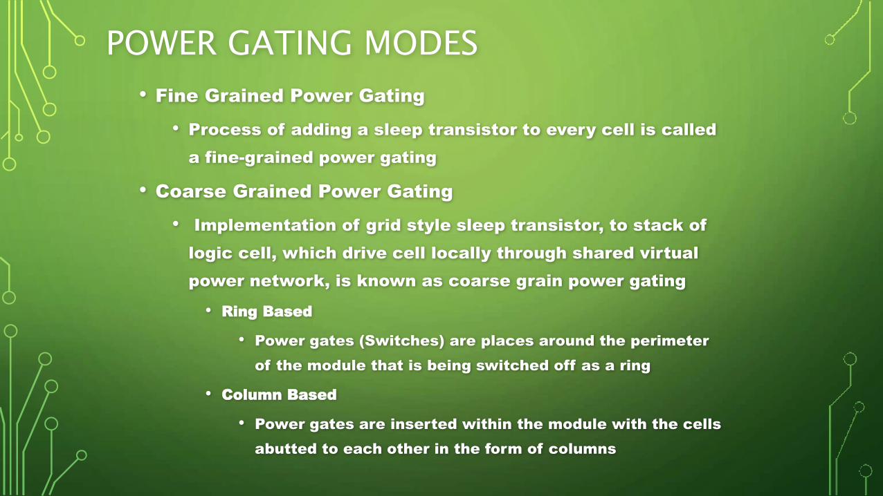
POWER GATING MODES
• Fine Grained Power Gating
• Process of adding a sleep transistor to every cell is called
a fine-grained power gating
• Coarse Grained Power Gating
• Implementation of grid style sleep transistor, to stack of
logic cell, which drive cell locally through shared virtual
power network, is known as coarse grain power gating
• Ring Based
• Power gates (Switches) are places around the perimeter
of the module that is being switched off as a ring
• Column Based
• Power gates are inserted within the module with the cells
abutted to each other in the form of columns

CONTROLLING MECHANISM
• Non-State Preserving Power Gating
• Cut-off (CO)
• Multi-Threshold (MTCMOS
• Boosted-Gate (BGMOS)
• Super Cut-off (SCCMOS)
• State Preserving Power Gating
• Variable Threshold (VTMOS)
• Zigzag Cut Off (ZZCO)
• Zero Delay Ripple Turn On (ZZRTO)
• State Preserving use some retention registers to store states.

STATE RETENTION TECHNIQUES
• When power gating taking place we have to retain some critical state
content (FSM State)
• Software Based Register Read and Write
• Scan Based approach based on using scan chains to store state off
chip
• Retention Registers

RETENTION REGISTERS
• When power gating taking place we have to retain some critical register content (FSM
State).
• Saving and restoring state quickly and efficiently is the faster and power efficient
method to get the block fully functional after power up.
• There can be various methods for state retention.
• DSP Unit: data flow driven DSP unit can start from reset on new data input.
• Cache Processor: This mechanism is good for large residual state retention.

SYNCHRONOUS & ASYNCRONOUS LOGIC POWER GATING
• Clock gating for dynamic power reduction which reduce the power consumption of
idle section of synchronous circuits
• Asynchronous circuits has a inherent strength of data driven capability and active
while performing useful tasks
• Asynchronous circuits implement the equivalent of a fine grain power gating network
• Power gating can be efficiently implemented in Pipelined flows

EDA POWER GATING
Designp power gating library cells
Determine which blocks to power gate
Determine state retention mechanism
Determine Rush Current Control Scheme
Design power gating controller
Power gating aware synthesis
Determine floor plan
power gating aware placement
clock tree synthesis
Route
Verify virtual rail electrical charateristics
verify timing