VLSI Design
Adder DesignAdder Design
ECE 4121 VLSI DEsign.1
[Adapted from Rabaey’s Digital Integrated Circuits, ©2002, J. Rabaey et al.]

Major Components of a Computer
Processor D iProcessor
Control
Devices
ControlMemory Input
Datapath Output
ECE 4121 VLSI DEsign.2

A Generic Digital Processor
MEMORYMEMORY
CONTROLOU
TPU
T
CONTROL
INPU
T-O
DATAPATH
ECE 4121 VLSI DEsign.3
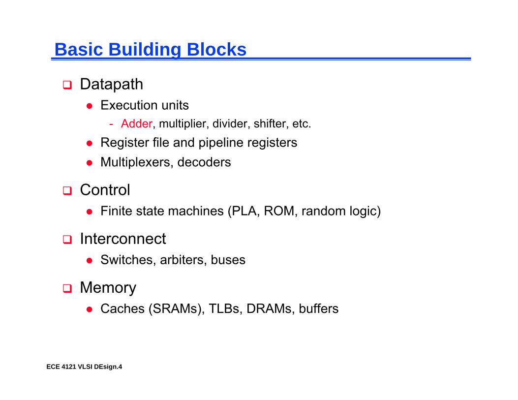
Basic Building Blocks
DatapathExecution units
- Adder multiplier divider shifter etc- Adder, multiplier, divider, shifter, etc.Register file and pipeline registersMultiplexers, decoders
ControlFinite state machines (PLA, ROM, random logic)
InterconnectSwitches, arbiters, buses
MemoryCaches (SRAMs), TLBs, DRAMs, buffers
ECE 4121 VLSI DEsign.4
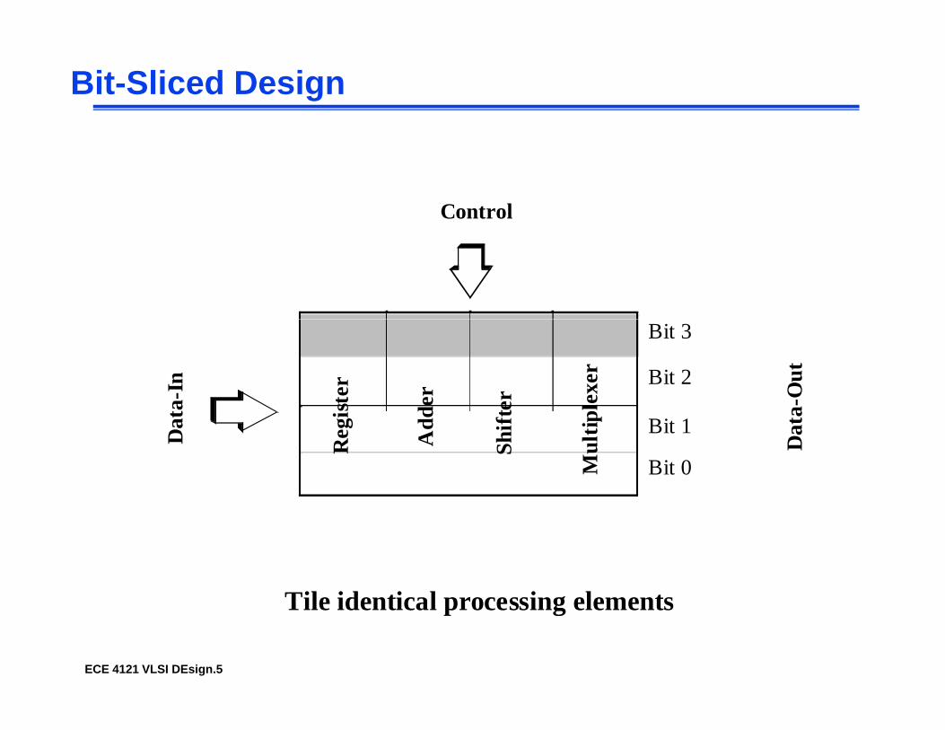
Bit-Sliced Design
Control
Bit 3
Bit 2
ster
der
ter
plex
er
ta-I
n
a-O
ut
Bit 1
Bit 0
Reg
i
Add
Shift
Mul
tipDat
Dat
a
Til id ti l i l t
ECE 4121 VLSI DEsign.5
Tile identical processing elements

Bit-Sliced Design
Control
Bit 3
Bit 2
ster
der
ter
plex
er
ta-I
n
a-O
ut
Bit 1
Bit 0
Reg
i
Add
Shift
Mul
tipDat
Dat
a
Til id ti l i l t
ECE 4121 VLSI DEsign.6
Tile identical processing elements

The 1-bit Binary AdderCi A B C C S carry status
1-bit Full Adder
AS
Cin A B Cin Cout S carry status0 0 0 0 0 kill0 0 1 0 1 kill0 1 0 0 1 propagateAdder
(FA)BS 0 1 0 0 1 propagate
0 1 1 1 0 propagate1 0 0 0 1 propagate1 0 1 1 0 propagate
C
S = A ⊕ B ⊕ C
p p g1 1 0 1 0 generate1 1 1 1 1 generate
Cout
G = ABP A ⊕ B = P ⊕ CS = A ⊕ B ⊕ Cin
Cout = AB + ACin + BCin (majority function)P = A ⊕ BK = !A !B
= P ⊕ Cin
= G + PCin
How can we use it to build a 64-bit adder?
How can we modify it easily to build an adder/subtractor?
ECE 4121 VLSI DEsign.7
How can we make it better (faster, lower power, smaller)?

One-Bit Full Adder: Share LogicAn observation
Almost always, sum = NOT carry
Cin A B Sum Cout0 0 0 0 0
i l d
0 0 1 1 00 1 0 1 0
includes 111 0 1 1 0 11 0 0 1 01 0 1 0 1Sum A B Cin + 1 0 1 0 11 1 0 0 11 1 1 1 1
Sum = A.B.Cin +(A+B+Cin).Cout
excludes 000
1 1 1 1 1
ECE 4121 VLSI DEsign.8

FA Gate Level Implementations
A B CinA B Cin
t1 t0t2 t0
t1t2
CoutS
Cout
S
ECE 4121 VLSI DEsign.9
S

Ripple Carry Adder (RCA)
A0 B0A1 B1A2 B2A3 B3
C0=CinFAFAFAFACout=C4
S0S1S2S3
Tadder ≈ TFA(A,B→Cout) + (N-2)TFA(Cin→Cout) + TFA(Cin→S)
t N 1( )t t+≈
T = O(N) worst case delayReal Goal: Make the fastest possible carry path
tadder N 1–( )tcarry tsum+≈
ECE 4121 VLSI DEsign.10
Real Goal: Make the fastest possible carry path

Complimentary Static CMOS Full Adder
VDDVDD
VDD
A B
B
Ci
A
BA
VDDCi
S
X
B
A
Ci ACi
B
VDD
SCi A
BBAA B Ci
Ci
A
Co B
Cout = AB + BCin + ACin SUM = ABC + !C (A + B + C )
28 Transistorsout in in
= AB + Cin(B + A) SUM = ABCin + !COUT(A + B + Cin)
ECE 4121 VLSI DEsign.11
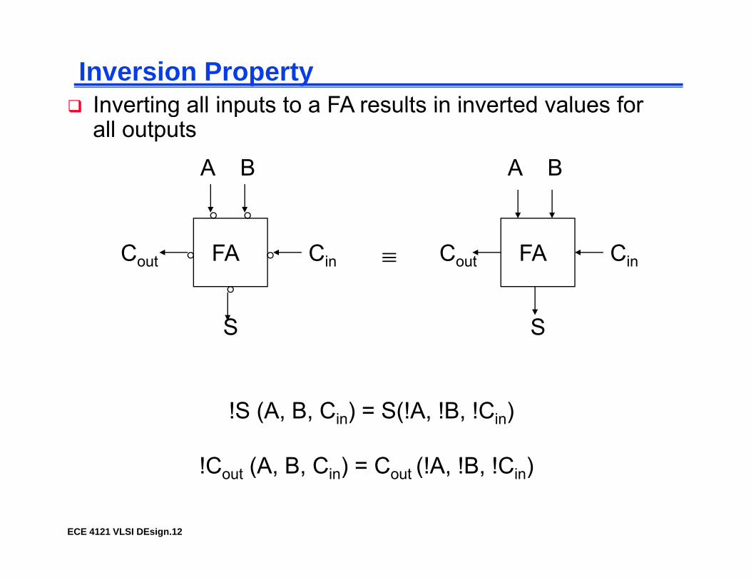
Inversion PropertyInverting all inputs to a FA results in inverted values for
A BA B
Inverting all inputs to a FA results in inverted values for all outputs
CFACFAC C ≡
S
CinFACout
S
FACout Cin ≡
SS
!Cout (A, B, Cin) = Cout (!A, !B, !Cin)
!S (A, B, Cin) = S(!A, !B, !Cin)
ECE 4121 VLSI DEsign.12
!Cout (A, B, Cin) Cout (!A, !B, !Cin)
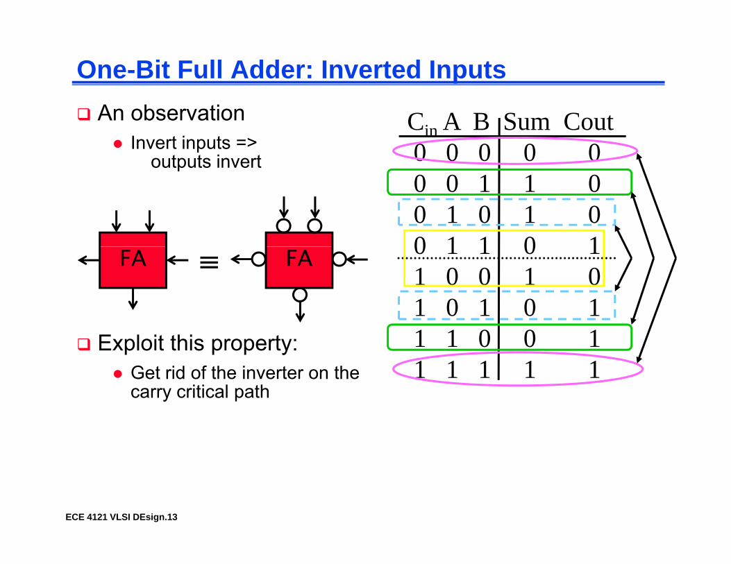
One-Bit Full Adder: Inverted InputsAn observation
Invert inputs =>outputs invert
Cin A B Sum Cout0 0 0 0 00 0 1 1 00 0 1 1 00 1 0 1 00 1 1 0 1FA 0 1 1 0 11 0 0 1 01 0 1 0 1
≡ FA
Exploit this property:Get rid of the inverter on the carry critical path
1 1 0 0 11 1 1 1 1
carry critical path
ECE 4121 VLSI DEsign.13

Exploiting the Inversion Property
A0 B0A1 B1A2 B2A3 B3
C0=CinFA’FA’FA’FA’Cout=C4
S0S1S2S3regular cellinverted cell regular cellinverted cell
Minimizes the critical path (the carry chain) by eliminating inverters between the FAs (will need toeliminating inverters between the FAs (will need to increase the transistor sizing on the carry chain portion of the mirror adder).
ECE 4121 VLSI DEsign.14

Ripple Carry Adder: Inverting Property
A1
B1
C2
A0
B0
C1
A2
B2
C
A3
B3
C4 C2C0
C1C3. . . FA’C4 FA’ FA’FA’
S1
S0
S2
S3
FA’ is similar to FA, but with no inverters on the outputsMuch faster (1-stage)Disadvantage: not regular data path
ECE 4121 VLSI DEsign.15

Mirror Adder 24+4 transistors
B B BB
A A ACin
24+4 transistors
kill888
6
6
444
A
A
CinCin
!Cout !S
kill0-propagate88 6
6
4
B B BA
A
A A
Cin
Cin
generate1-propagate
4 4
4 4
4 2 2 23
32
B
C = AB + BC + AC SUM = ABC + !C (A + B + C )
3
Cout = AB + BCin + ACin= AB + Cin(B + A)
SUM = ABCin + !COUT(A + B + Cin)
Sizing: Each input in the carry circuit has a logical effort of 2 so the optimal fan-out for each is also 2. Since !Cout drives 2 internal and 2
ECE 4121 VLSI DEsign.16
optimal fan out for each is also 2. Since !Cout drives 2 internal and 2 inverter transistor gates (to form Cin for the nms bit adder) should oversize the carry circuit. PMOS/NMOS ratio of 2.

Mirror Adder FeaturesThe NMOS and PMOS chains are completelyThe NMOS and PMOS chains are completely symmetrical with a maximum of two series transistors in the carry circuitry, guaranteeing identical rise and fall transitions if the NMOS and PMOS devices are properlytransitions if the NMOS and PMOS devices are properly sized.
When laying out the cell the most critical issue is theWhen laying out the cell, the most critical issue is the minimization of the capacitances at node !Cout (four diffusion capacitances, two internal gate capacitances, and two inverter gate capacitances) Shared diffusionsand two inverter gate capacitances). Shared diffusions can reduce the stack node capacitances.
The transistors connected to Cin are placed closest to the in poutput.
Only the transistors in the carry stage have to be
ECE 4121 VLSI DEsign.17
optimized for optimal speed. All transistors in the sum stage can be minimal size.

A 64-bit Adder/Subtractordd/ bt
1-bit FA S0
C0=CinRipple Carry Adder (RCA) built out of 64 FAs A0
B
add/subt
C1
1-bit FA S1
Subtraction – complement all subtrahend bits (xor gates) and set the low
B0
A1
BC2
1-bit FA S2
gates) and set the low order carry-in
RCA
B1
A2
B C3
C
. . .advantage: simple logic,
so small (low cost)
B2
1-bit FA S63
C63disadvantage: slow (O(N) for N bits) and lots of glitching (so lots of energy consumption)
A63
B63
ECE 4121 VLSI DEsign.18
C64=Coutconsumption) B63
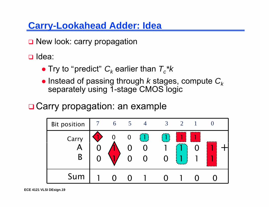
Carry-Lookahead Adder: IdeaNew look: carry propagation
Idea:Try to “predict” Ck earlier than Tc*kInstead of passing through k stages, compute Ckseparately using 1-stage CMOS logicseparately using 1 stage CMOS logic
Carry propagation: an example
Bit position
Carry
7 6 5 4 3 2 1 0
1 0 0 1 1 1 1 A B
0 1 0 0 1 1 0 1 +0 1 0 0 0 1 1 1
ECE 4121 VLSI DEsign.19
Sum 1 0 0 1 0 1 0 0

Carry-Lookahead Adder (CLA): One Bit
(kill)
What happens to thepropagating carry inbit position k?
0 0 0A B Cin Cout
0-propagate kill
(kill)(propagate)(propagate)
0 0 - 00 1 C C1 0 C C(propagate)
(generate)1 0 C C1 1 - 1A B A
CB
BCout
p = A+B (or A ⊕ B)
A B AB p = A+B (or A ⊕ B)
g = A.B
ECE 4121 VLSI DEsign.20
1-propagate generate [Rab96] p391

CLA: Propagation Equationsf CIf C4=1, then either:
g3 generated at bit pos 3g2.p3 generated at bit pos 2, propagated 3g2.p3 generated at bit pos 2, propagated 3g1.p2.p3 generated at bit pos 1, propagated 2,3g0.p1.p2.p3 generated at bit pos 0, propagated 1,2,3C i d 0 1 2 3Cin.p0.p1.p2.p3 input carry, propagated 0,1,2,3
C4 = g3+ g2.p3 + g1.p2.p3 + g0.p1.p2.p3 + Cin.p0.p1.p2.p3
Implement Implement CC44 as a oneas a one--stage CMOS logicstage CMOS logicdelay=1 (or is it?)delay=1 (or is it?)
ECE 4121 VLSI DEsign.21

CLA: Static Logic Implementation
p1.g2.g3 C4
gg3d
e qo
gg1
g2ef
h srq
C
g0
C4
hj
s
tp0p
Cink
l
tu
p g C
p1p2p3
lm
n
vwx
ECE 4121 VLSI DEsign.22
p3.g2 C4p3 nx

CLA: Dynamic Logic ImplementationDynamic gate implementation:
C4 = g3+ p3 . (g2 + p2 . (g1 + p1 . (g0 + P0.Cin)))
6 transistors6 transistors C4p3 g
φ
in seriesin series
p
p2
p3
g2
g3
p0
p1
g0
g1
Cin
φ
ECE 4121 VLSI DEsign.23
[©Hauck][WE92] p529
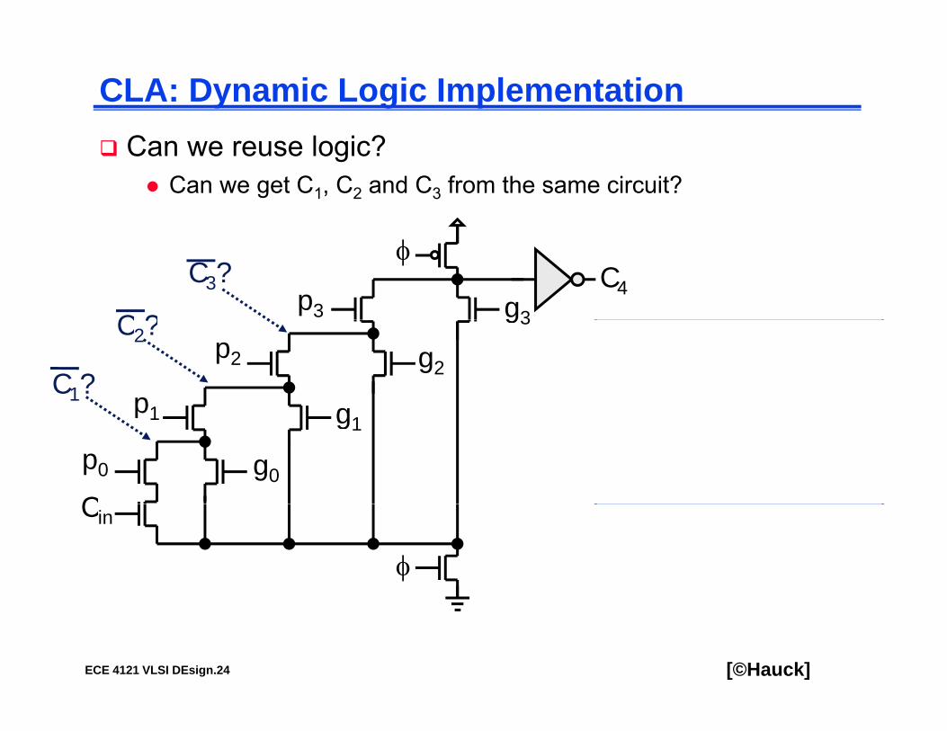
CLA: Dynamic Logic ImplementationC ?Can we reuse logic?
Can we get C1, C2 and C3 from the same circuit?
C4p3 g3
φ
C ?
C3?
p1
p2
g
g2
g3
C1?
C2? No!No!C1, C2 and C3C1, C2 and C3
b f ib f i
C
p0
p1
g0
g1 may be floatingmay be floating(not precharged)(not precharged)
Cin
φ Charge sharingCharge sharingproblemproblem
ECE 4121 VLSI DEsign.24 [©Hauck]
problemproblem
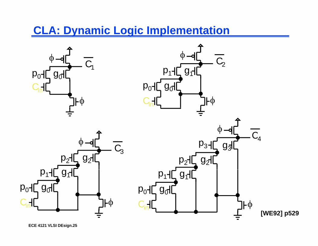
CLA: Dynamic Logic Implementation
φC1
g0p0p1 g1
φC2
φ
g0p0
Cin g0p0
Cin φ
φφ
C4
pp2
gg2
φC3
p2
p3
g2
g3
C4
p1 g1
g0p0
C φ
p1 g1
g0p0
C φ
ECE 4121 VLSI DEsign.25
[WE92] p529Cin φ Cin φ

CLA: Basic Block (4 Bits) Architecturef CBlock of 4-bit p, g, Cout
A B0A B1A B2A B30123
p,g p,g p,g p,g
C0
p0 g0p1 g1p2 g2p3 g3
C4 0
C1C2
C4
2C3
ECE 4121 VLSI DEsign.26
S0
S1
S2
S3

CLA: N-Bit ArchitecturePut it all together:
B0A0A1 B1A2 B2A3 B3A4A5 B5A6 B6A7 B7 B4… B0A0A1 B1A2 B2A3 B3
p,g p,g p,g p,g
A4A5 B5A6 B6A7 B7
p,g p,g p,g p,g
B4
…
…
C0… Carry Generator Carry Generator
C4C8
S0S1S2S3
C4
S4S5S6S7
C8…
ECE 4121 VLSI DEsign.27

CLA: 12-Bit Example1101 1001 1010A
B0B1B2B3B5B6B7 B4B9B10A0A1A2A3A4A5A6A7A8A9A10A11B11 B8
01111101
01101001
11011010
B=A=
p,g p,g p,g p,gp,g p,g p,g p,g
C0
p,g p,g p,g p,g 00
C
Carry Generator Carry Generator
C
Carry Generator
C
S0S1S2S3S4S5S6S7
C4C8
S8S9S10S11
C12
00000 00000 00000T=0 00000 00000 00000T=001001 11110 01111T=201001 00001 01111T=3
ECE 4121 VLSI DEsign.28
T 301011 00001 01111T=4
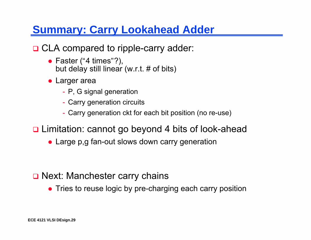
Summary: Carry Lookahead AdderCCLA compared to ripple-carry adder:
Faster (“4 times”?),but delay still linear (w.r.t. # of bits)Larger area
- P, G signal generation- Carry generation circuitsy g- Carry generation ckt for each bit position (no re-use)
Limitation: cannot go beyond 4 bits of look-aheadLarge p,g fan-out slows down carry generation
Next: Manchester carry chainsTries to reuse logic by pre-charging each carry position
ECE 4121 VLSI DEsign.29

Recap: Carry Look-AheadCCharge sharing problem
C4p3 g
φC3?
p
p2
p3
g2
g3
C1?
C2?
p0
p1
g0
g1
Cin
φ
ECE 4121 VLSI DEsign.30
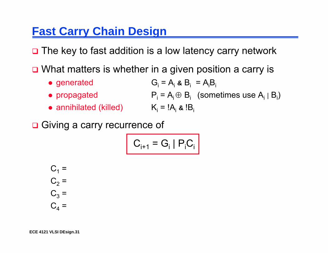
Fast Carry Chain DesignfThe key to fast addition is a low latency carry network
What matters is whether in a given position a carry isgenerated Gi = Ai & Bi = AiBi
propagated Pi = Ai ⊕ Bi (sometimes use Ai | Bi)annihilated (killed) Ki = !Ai & !Bi( ) i i i
Giving a carry recurrence of
C = G | P CCi+1 = Gi | PiCi
C1 =C2 = C3 =C =
ECE 4121 VLSI DEsign.31
C4 =

Fast Carry Chain DesignfThe key to fast addition is a low latency carry network
What matters is whether in a given position a carry isgenerated Gi = Ai & Bi = AiBi
propagated Pi = Ai ⊕ Bi (sometimes use Ai | Bi)annihilated (killed) Ki = !Ai & !Bi( ) i i i
Giving a carry recurrence of
C = G | P CCi+1 = Gi | PiCi
C1 = G0 | P0C0
C2 = G1 | P1G0 | P1P0 C0
C3 = G2 | P2G1 | P2P1G0 | P2P1P0 C0
C = G | P G | P P G | P P P G | P P P P C
ECE 4121 VLSI DEsign.32
C4 = G3 | P3G2 | P3P2G1 | P3P2P1G0 | P3P2P1P0 C0
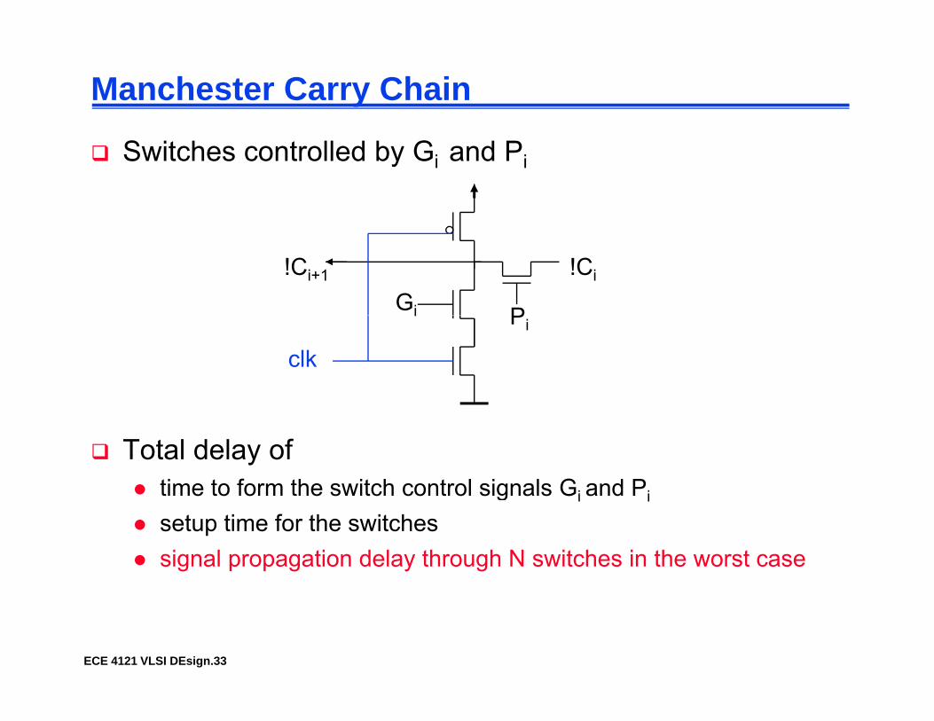
Manchester Carry Chain
Switches controlled by Gi and Pi
Gi P
!Ci!Ci+1
i Pi
clk
Total delay oftime to form the switch control signals Gi and Pig i i
setup time for the switchessignal propagation delay through N switches in the worst case
ECE 4121 VLSI DEsign.33
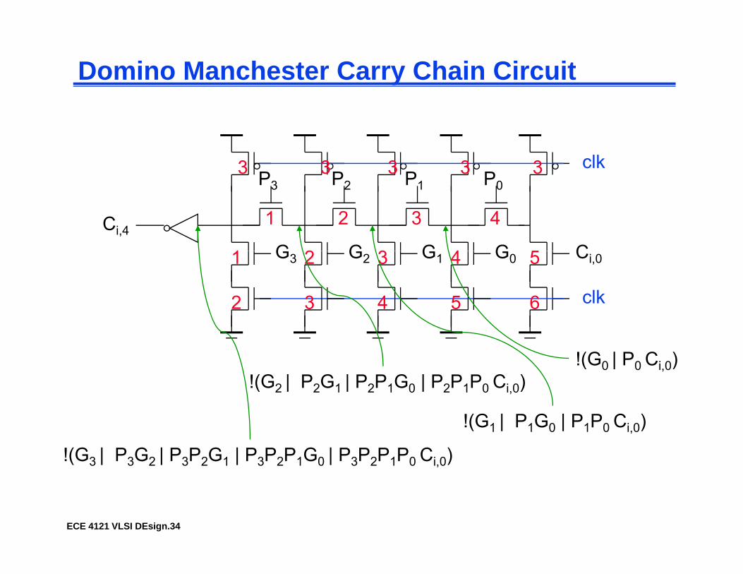
Domino Manchester Carry Chain Circuit
clkPPPP3 3 3 3 3
CG
P0P1P2P3
GGGCi,4
1 2 3 4
51 2 3 4 Ci,0G0
clk
G1G2G3 5
6
1
2
2
3
3
4
4
5
!(G0 | P0 Ci,0)!(G2 | P2G1 | P2P1G0 | P2P1P0 Ci,0)
!(G1 | P1G0 | P1P0 Ci,0)
!(G3 | P3G2 | P3P2G1 | P3P2P1G0 | P3P2P1P0 Ci,0)
ECE 4121 VLSI DEsign.34
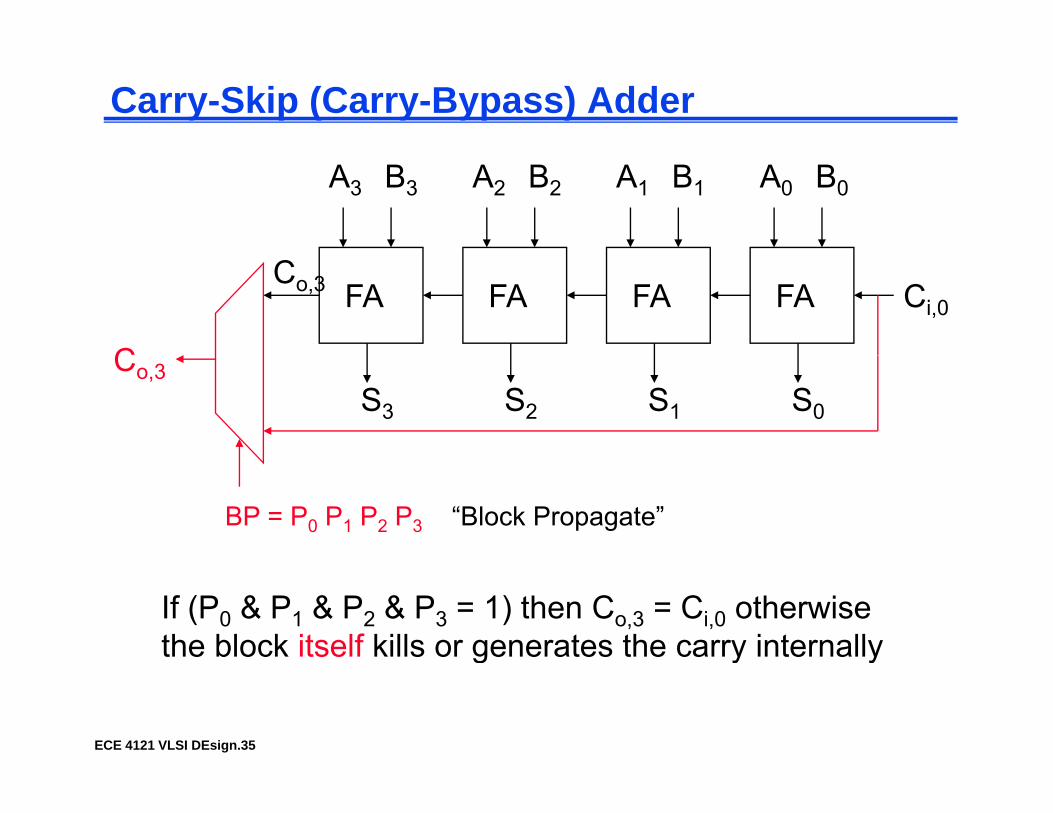
Carry-Skip (Carry-Bypass) Adder
A0 B0A1 B1A2 B2A3 B3
Ci,0FAFAFAFACo,3
CS0S1S2S3
Co,3
BP = P0 P1 P2 P3 “Block Propagate”
If (P0 & P1 & P2 & P3 = 1) then Co,3 = Ci,0 otherwise the block itself kills or generates the carry internally
ECE 4121 VLSI DEsign.35
g y y
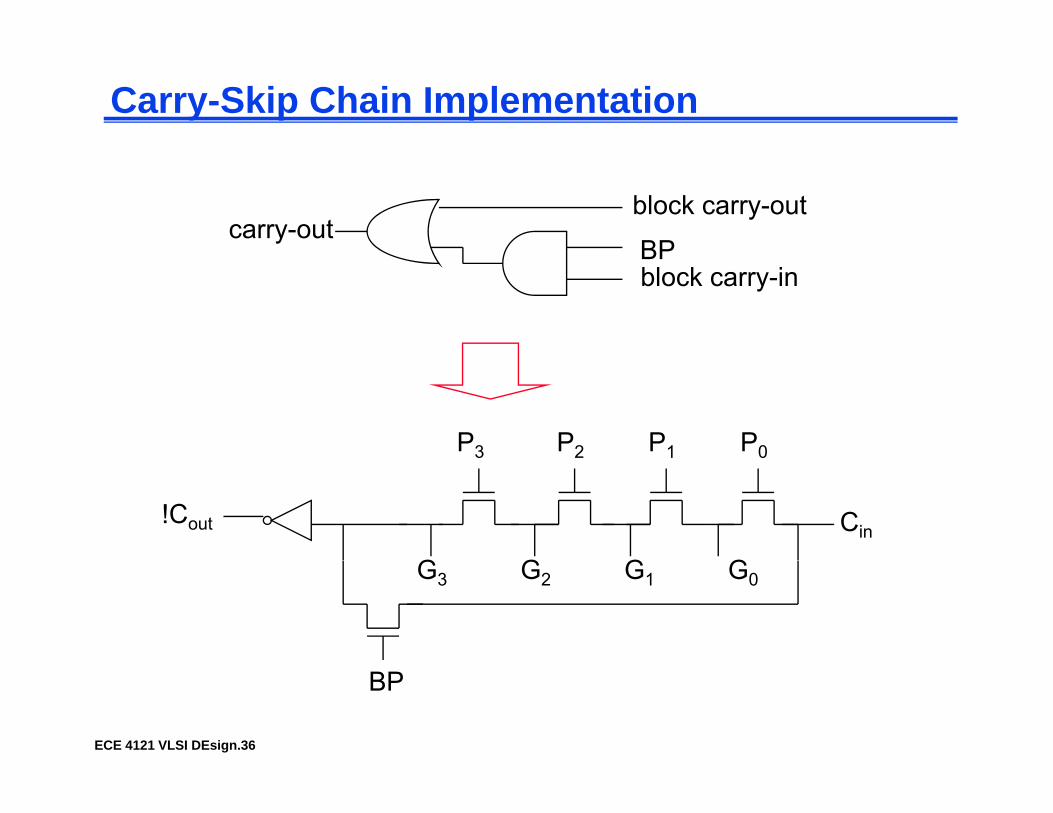
Carry-Skip Chain Implementation
BP
block carry-outcarry-out
BPblock carry-in
P0P1P2P3
Cin
GGGG
!Cout
G0G1G2G3
ECE 4121 VLSI DEsign.36
BP

4-bit Block Carry-Skip Adderbits 0 to 3bits 4 to 7bits 8 to 11bits 12 to 15
SetupSetupSetupSetup
bits 0 to 3bits 4 to 7bits 8 to 11bits 12 to 15
Ci,0
CarryPropagation
CarryPropagation
CarryPropagation
CarryPropagation
SumSumSumSum
Worst-case delay → carry from bit 0 to bit 15 = carry generated in bit 0, ripples through bits 1, 2, and 3, skips the middle two groups (B is the group size in bits) ripples in the last group fromgroups (B is the group size in bits), ripples in the last group from bit 12 to bit 15
T = t + B t + ((N/B) 1) t +B t + t
ECE 4121 VLSI DEsign.37
Tadd = tsetup + B tcarry + ((N/B) -1) tskip +B tcarry + tsum
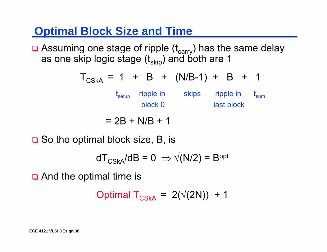
Optimal Block Size and TimeAssuming one stage of ripple (t ) has the same delayAssuming one stage of ripple (tcarry) has the same delay as one skip logic stage (tskip) and both are 1
TCSkA = 1 + B + (N/B-1) + B + 1TCSkA 1 + B + (N/B 1) + B + 1tsetup ripple in skips ripple in tsum
block 0 last block
= 2B + N/B + 1
So the optimal block size, B, isSo the optimal block size, B, is
dTCSkA/dB = 0 ⇒ √(N/2) = Bopt
A d th ti l ti iAnd the optimal time is
Optimal TCSkA = 2(√(2N)) + 1
ECE 4121 VLSI DEsign.38

Carry-Skip Adder ExtensionsVariable block sizesVariable block sizes
A carry that is generated in, or absorbed by, one of the inner blocks travels a shorter distance through the skip blocks, so can have bigger blocks for the inner carries without increasing the a e b gge b oc s o t e e ca es t out c eas g t eoverall delay
CinCout
Multiple levels of skip logicMultiple levels of skip logic
CinCout
skip level 1
skip level 2AND of the fi t l l ki
ECE 4121 VLSI DEsign.39
skip level 2 first level skip signals (BP’s)
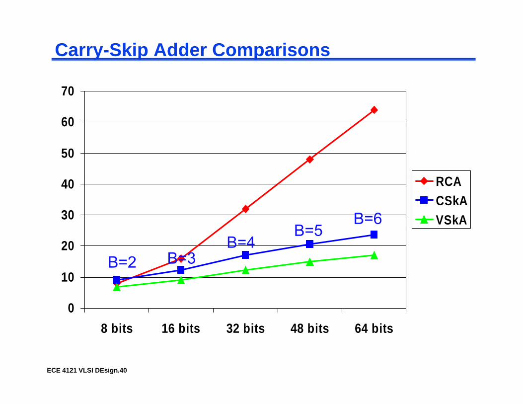
Carry-Skip Adder Comparisons
60
70
50
60
RCA
30
40 RCACSkAVSkA
B 5B=6
10
20B=2 B=3
B=4B=5
0
10
8 bits 16 bits 32 bits 48 bits 64 bits
ECE 4121 VLSI DEsign.40
8 bits 16 bits 32 bits 48 bits 64 bits

Carry Select AdderA’s B’s
4-b Setupp
“0” carry propagation 0
P’s G’sPrecompute the carry out of each block for both carry in = 0 and y p p g
“1” carry propagation 1
both carry_in 0 and carry_in = 1 (can be done for all blocks in parallel) and then select y p p g
multiplexer CinCout
parallel) and then select the correct one
inCout
Sum generationC’s
ECE 4121 VLSI DEsign.41S’s
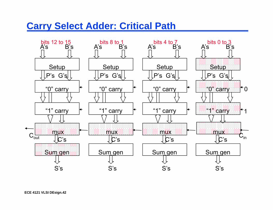
Carry Select Adder: Critical Path
S t
A’s B’s
S t
A’s B’s
S t
A’s B’s
S t
A’s B’sbits 0 to 3bits 4 to 7bits 8 to 1bits 12 to 15
Setup
“0” carry 0
P’s G’sSetup
“0” carry
P’s G’sSetup
“0” carry
P’s G’sSetup
“0” carry
P’s G’s
y
“1” carry 1
y
“1” carry
y
“1” carry
y
“1” carry
mux CinC’smux
C’smux
C’smuxCout C’s
Sum gen
S’s
Sum gen
S’s
Sum gen
S’s
Sum gen
S’s
ECE 4121 VLSI DEsign.42

Carry Select Adder: Critical Path
S t
A’s B’s
S t
A’s B’s
S t
A’s B’s
S t
A’s B’sbits 0 to 3bits 4 to 7bits 8 to 1bits 12 to 15
1Setup
“0” carry 0
P’s G’sSetup
“0” carry
P’s G’sSetup
“0” carry
P’s G’sSetup
“0” carry
P’s G’s
y
“1” carry 1
y
“1” carry
y
“1” carry
y
“1” carry
+4
mux CinC’smux
C’smux
C’smuxCout C’s
+1+1+1+1
Sum gen
S’s
Sum gen
S’s
Sum gen
S’s
Sum gen
S’s
+1
ECE 4121 VLSI DEsign.43
Tadd = tsetup + B tcarry + N/B tmux + tsum

Square Root Carry Select Adder bits 0 to 1bits 2 to 4bit 5 t 8bit 9 t 13bits 14 to 19
Setup
A’s B’sA’s B’s
Setup
A’s B’s
Setup
A’s B’sbits 0 to 1bits 2 to 4bits 5 to 8bits 9 to 13
SetupSetup
A’s B’sbits 14 to 19
Setup
“0” carry 0
P’sG’sSetup
“0” carry
P’s G’sSetup
“0” carry
P’s G’sSetupP’s G’s
“0” carry
Setup
“0” carry
P’s G’s
“1” carry 1“1” carry“1” carry “1” carry“1” carry
mux CinC’smux
C’smuxCout
C’smux
C’smux
C’s
Sum gen
S’sS’s
Sum genSum gen
S’s
Sum gen
S’s
Sum gen
S’s
ECE 4121 VLSI DEsign.44
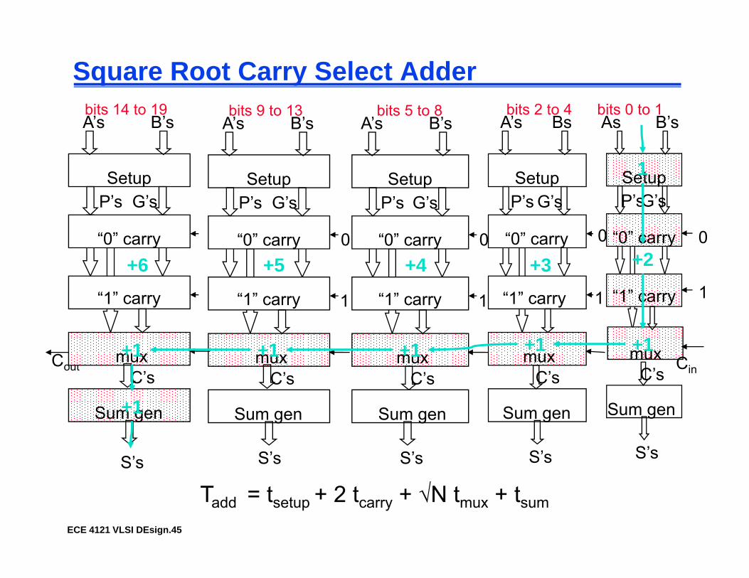
Square Root Carry Select Adder bits 0 to 1bits 2 to 4bit 5 t 8bit 9 t 13bits 14 to 19
Setup
As B’sA’s Bs
Setup
A’s B’s
Setup
A’s B’sbits 0 to 1bits 2 to 4bits 5 to 8bits 9 to 13
SetupSetup
A’s B’sbits 14 to 19
1Setup
“0” carry 0
P’sG’s
0
Setup
“0” carry
P’s G’sSetup
“0” carry 0
P’s G’sSetup
0
P’s G’s
“0” carry
Setup
“0” carry
P’s G’s
2
“1” carry 11“1” carry“1” carry 1 1“1” carry“1” carry
+2+3+4+5+6
mux CinC’smux
C’smuxCout
C’smux
C’smux
C’s
+1+1+1+1+1
Sum gen
S’sS’s
Sum genSum gen
S’s
Sum gen
S’s
Sum gen+1
S’s
ECE 4121 VLSI DEsign.45
Tadd = tsetup + 2 tcarry + √N tmux + tsum

Parallel Prefix Adders (PPAs)Define carry operator € on (G P) signal pairsDefine carry operator € on (G,P) signal pairs
(G’’,P’’) (G’,P’)G’’
€
(G P)
whereG = G’’ ∨ P’’G’
G’!G
P’’(G,P) P = P’’P’P
€ is associative, i.e.,[(g’’’,p’’’) € (g’’,p’’)] € (g’,p’) = (g’’’,p’’’) € [(g’’,p’’) € (g’,p’)]
€
€ €
€
ECE 4121 VLSI DEsign.46
€ €

PPA General StructureGiven P and G terms for each bit position computing allGiven P and G terms for each bit position, computing all the carries is equal to finding all the prefixes in parallel
(G0,P0) € (G1,P1) € (G2,P2) € … € (GN-2,PN-2) € (GN-1,PN-1)( 0, 0) ( 1, 1) ( 2, 2) ( N-2, N-2) ( N-1, N-1)
Since € is associative, we can group them in any order but note that it is not commutative
Measures to considerb f € ll
Pi, Gi logic (1 unit delay)number of € cellstree cell depth (time)tree cell areaCi parallel prefix logic tree
(1 unit delay per level) cell fan-in and fan-outmax wiring lengthwiring congestion
(1 unit delay per level)
ECE 4121 VLSI DEsign.47
delay path variation (glitching)Si logic (1 unit delay)
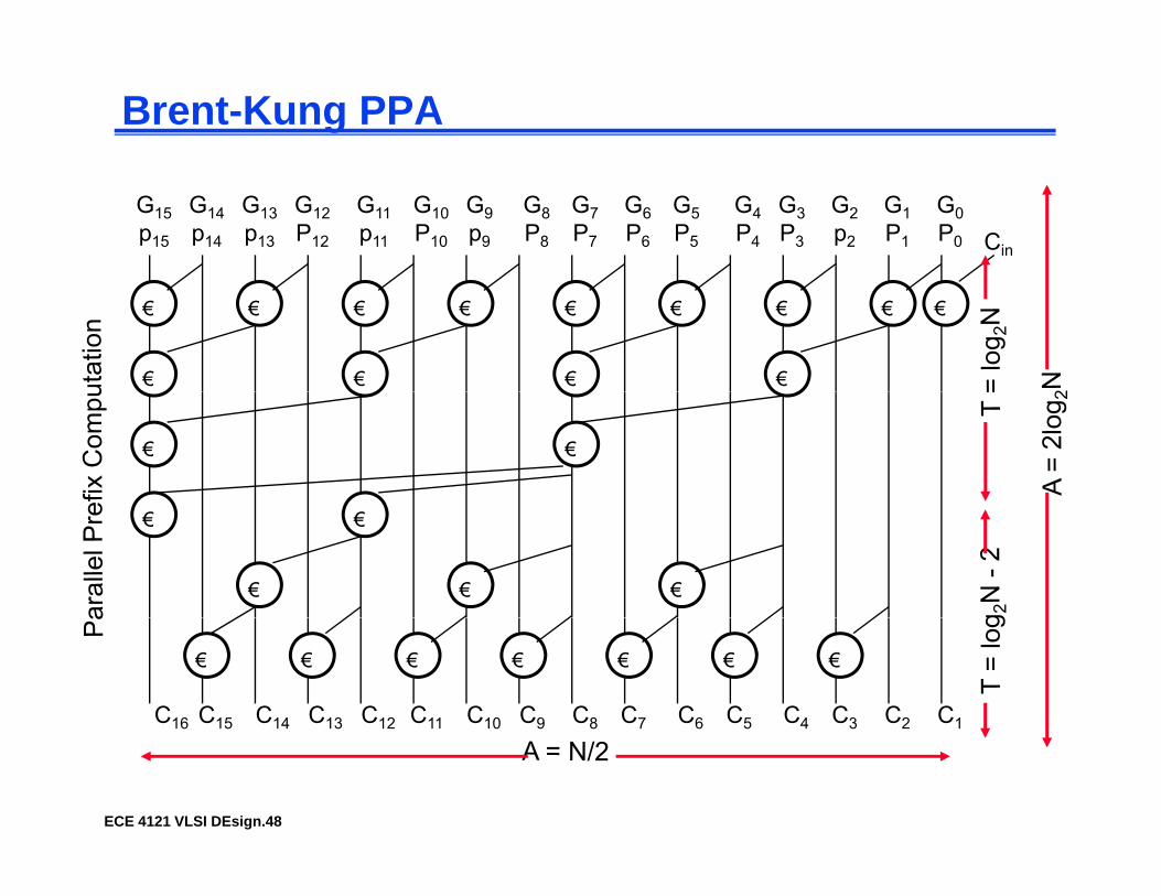
Brent-Kung PPA
G0P0
G1P1
G2p2
G3P3
G4P4
G5P5
G6P6
G7P7
G8P8
G9p9
G10P10
G11p11
G12P12
G13p13
G14p14
G15p15 Cin
€€€€€€€€
€ € € €
€
€ €
€ €
€ € €
€ € € € € € €
C1C2C3C4C5C6C7C8C9C10C11C12C13C14C15C16
ECE 4121 VLSI DEsign.48
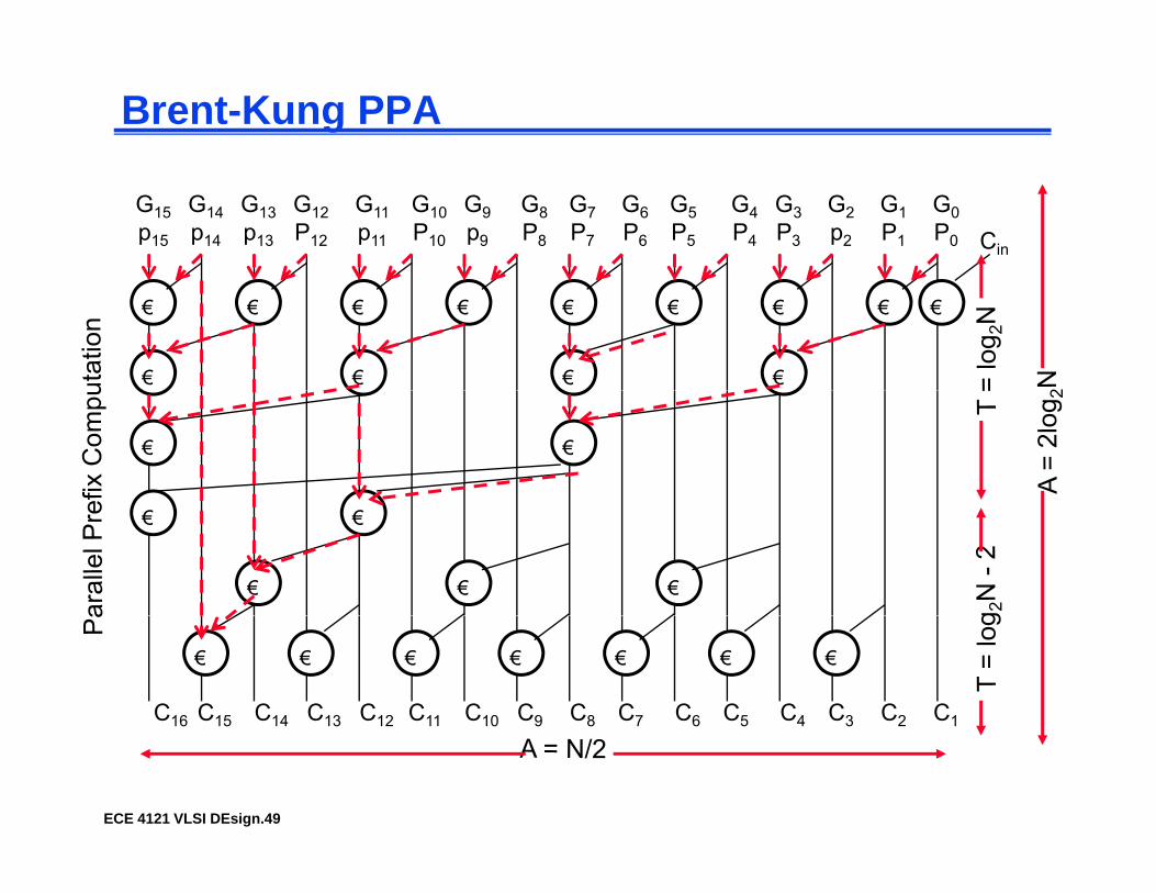
Brent-Kung PPA
G0P0
G1P1
G2p2
G3P3
G4P4
G5P5
G6P6
G7P7
G8P8
G9p9
G10P10
G11p11
G12P12
G13p13
G14p14
G15p15 Cin
€€€€€€€€
€ € € €
€
€ €
€ €
€ € €
€ € € € € € €
C1C2C3C4C5C6C7C8C9C10C11C12C13C14C15C16
ECE 4121 VLSI DEsign.49
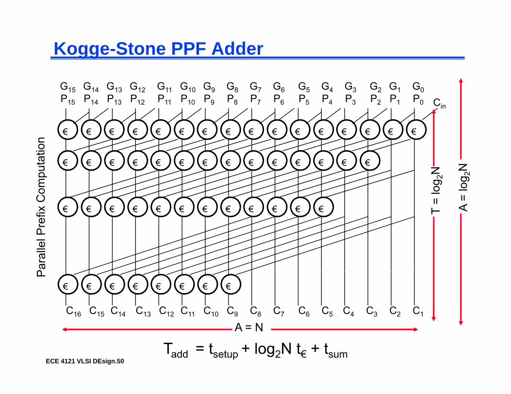
Kogge-Stone PPF Adder
G0P0
G1P1
G2P2
G3P3
G4P4
G5P5
G6P6
G7P7
G8P8
G9P9
G10P10
G11P11
G12P12
G13P13
G14P14
G15P15 Cin
€€€€€€€€
€ € € €
€€€€€€€€
€ € € € € € € € € €
€ €€ € € € € € € € € €
€ €
C1C2C3C4C5C6C7C8C9C10C11C12C13C14C15C16
€ € € € € €
ECE 4121 VLSI DEsign.50Tadd = tsetup + log2N t€ + tsum
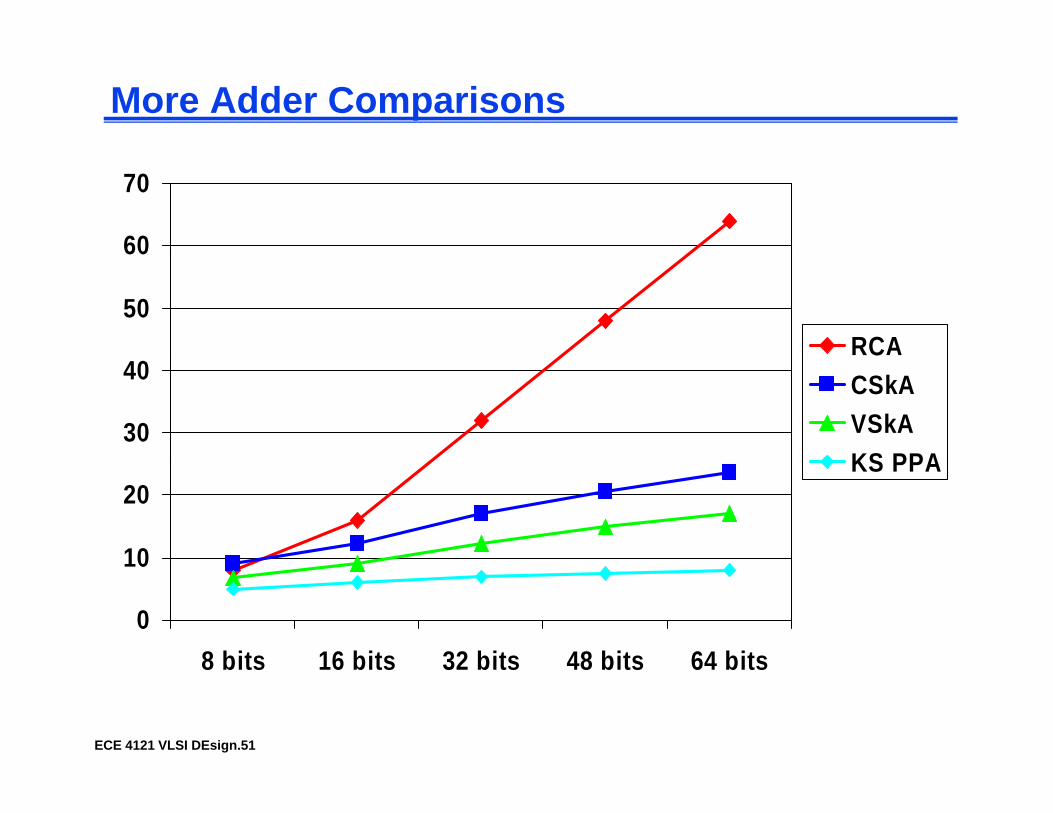
More Adder Comparisons
60
70
50
60
RCA
30
40C
CSkAVSkAKS PPA
10
20KS PPA
0
10
8 bits 16 bits 32 bits 48 bits 64 bits
ECE 4121 VLSI DEsign.51
8 bits 16 bits 32 bits 48 bits 64 bits
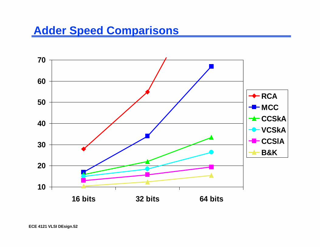
Adder Speed Comparisons
70
50
60
RCAMCC
40
MCCCCSkAVCSkACCSlA
20
30 CCSlAB&K
1016 bits 32 bits 64 bits
ECE 4121 VLSI DEsign.52
6 b ts 3 b ts 6 b ts

Adder Average Power Comparisons
30
35
25 RCAMCC
15
20 CCSkAVCSkACCSlA
5
10CCSlAB&K
0
5
16 bits 32 bits 64 bits
ECE 4121 VLSI DEsign.53
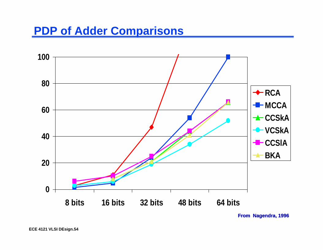
PDP of Adder Comparisons
100
60
80RCAMCCA
40
60CCSkAVCSkACCSlA
20
CCSlABKA
08 bits 16 bits 32 bits 48 bits 64 bits
ECE 4121 VLSI DEsign.54
8 bits 16 bits 32 bits 48 bits 64 bitsFrom Nagendra, 1996From Nagendra, 1996
Recommended