Embed Size (px)
Citation preview

VLSI Design
g

VLSI Design
i
About the Tutorial
Over the past several years, Silicon CMOS technology has become the dominant fabrication
process for relatively high performance and cost effective VLSI circuits. The revolutionary
nature of these developments is understood by the rapid growth in which the number of
transistors integrated on circuit on single chip. In this tutorial we are providing concept of
MOS integrated circuits and coding of VHDL and Verilog language.
Audience
This reference has been prepared for the students who want to know about the VLSI
Technology. The students will be able to know about the VHDL and Verilog program coding.
Prerequisites
Before you start proceeding with this tutorial, we make an assumption that you are already
aware of the basic concepts of basic concept of Digital Electronics.
Copyright & Disclaimer
Copyright 2015 by Tutorials Point (I) Pvt. Ltd.
All the content and graphics published in this e-book are the property of Tutorials Point (I)
Pvt. Ltd. The user of this e-book is prohibited to reuse, retain, copy, distribute or republish
any contents or a part of contents of this e-book in any manner without written consent
of the publisher.
We strive to update the contents of our website and tutorials as timely and as precisely as
possible, however, the contents may contain inaccuracies or errors. Tutorials Point (I) Pvt.
Ltd. provides no guarantee regarding the accuracy, timeliness or completeness of our
website or its contents including this tutorial. If you discover any errors on our website or
in this tutorial, please notify us at [email protected]
VLSI Design
ii
Table of Contents
About the Tutorial ............................................................................................................................................ i Audience ........................................................................................................................................................... i Prerequisites ..................................................................................................................................................... i Copyright & Disclaimer ..................................................................................................................................... i Table of Contents ............................................................................................................................................ ii
PART 1 – VLSI BASICS .................................................................................................................. 1
1. VLSI – Digital System ................................................................................................................................. 2 VLSI Design Flow .............................................................................................................................................. 2 Y Chart ............................................................................................................................................................. 4 Design Hierarchy-Structural ............................................................................................................................ 4
2. VLSI – FPGA Technology ............................................................................................................................ 7 FPGA – Introduction ........................................................................................................................................ 7 Gate Array Design ............................................................................................................................................ 8 Standard Cell Based Design ............................................................................................................................. 9 Full Custom Design ........................................................................................................................................ 10
3. VLSI – MOS Transistor ............................................................................................................................. 11 Structure of a MOSFET .................................................................................................................................. 11 Working of a MOSFET .................................................................................................................................... 14 MOSFET Current – Voltage Characteristics ................................................................................................... 16
4. VLSI – MOS Inverter ................................................................................................................................ 19 Principle of Operation ................................................................................................................................... 19 Resistive Load Inverter .................................................................................................................................. 20 Inverter with N type MOSFET Load ............................................................................................................... 22 Enhancement Load NMOS ............................................................................................................................. 22 Depletion Load NMOS ................................................................................................................................... 23 CMOS Inverter – Circuit, Operation and Description .................................................................................... 24
5. VLSI – Combinational MOS Logic Circuits ................................................................................................ 28 CMOS Logic Circuits ....................................................................................................................................... 28 Complex Logic Circuits ................................................................................................................................... 31 Complex CMOS Logic Gates ........................................................................................................................... 32
6. VLSI – Sequential MOS Logic Circuits ....................................................................................................... 36 CMOS Logic Circuits ....................................................................................................................................... 37 CMOS Logic Circuits ....................................................................................................................................... 40
PART 2 – VHDL .......................................................................................................................... 44
7. VHDL – Introduction................................................................................................................................ 45 Data Flow Modeling ...................................................................................................................................... 46 Behavioral Modeling ..................................................................................................................................... 46 Structural Modeling ....................................................................................................................................... 46 Logic Operation – AND GATE ......................................................................................................................... 47 Logic Operation – OR Gate ............................................................................................................................ 48 Logic Operation – NOT Gate .......................................................................................................................... 48
VLSI Design
iii
Logic Operation – NAND Gate ....................................................................................................................... 49 Logic Operation – NOR Gate .......................................................................................................................... 50 Logic Operation – XOR Gate .......................................................................................................................... 51 Logic Operation – X-NOR Gate ...................................................................................................................... 52
8. VHDL – Programming for Combinational Circuits .................................................................................... 54 VHDL Code for a Half-Adder .......................................................................................................................... 54 VHDL Code for a Full Adder ........................................................................................................................... 54 VHDL Code for a Half-Subtractor ................................................................................................................... 55 VHDL Code for a Full Subtractor .................................................................................................................... 56 VHDL Code for a Multiplexer ......................................................................................................................... 56 VHDL Code for a Demultiplexer ..................................................................................................................... 57 VHDL Code for a 8 x 3 Encoder: ..................................................................................................................... 58 VHDL Code for a 3 x 8 Decoder ..................................................................................................................... 58 VHDL Code – 4 bit Parallel adder ................................................................................................................... 59 VHDL Code – 4 bit Parity Checker .................................................................................................................. 61 VHDL Code – 4 bit Parity Generator .............................................................................................................. 61
9. VHDL – Programming for Sequential Crcuits ........................................................................................... 63 VHDL Code for an SR Latch ............................................................................................................................ 63 VHDL Code for a D Latch................................................................................................................................ 63 VHDL Code for an SR Flip Flop ....................................................................................................................... 64 VHDL code for a JK Flip Flop .......................................................................................................................... 65 VHDL Code for a D Flip Flop ........................................................................................................................... 66 VHDL Code for a T Flip Flop ........................................................................................................................... 67 VHDL Code for a 4 - bit Up Counter ............................................................................................................... 68 VHDL Code for a 4-bit Down Counter ............................................................................................................ 69
PART 3 – VERILOG ..................................................................................................................... 71
10. Verilog – Introduction ............................................................................................................................. 72 Behavioral level ............................................................................................................................................. 72 Register−Transfer Level ................................................................................................................................. 72 Gate Level ...................................................................................................................................................... 72 Lexical Tokens ................................................................................................................................................ 72 Gate Level Modelling ..................................................................................................................................... 73 Data Types ..................................................................................................................................................... 75 Operators ...................................................................................................................................................... 77 Operands ....................................................................................................................................................... 81 Modules ......................................................................................................................................................... 82
11. Verilog – Behavioral Modelling & Timing Control ................................................................................... 84 Procedural Assignments ................................................................................................................................ 84 Delay in Assignment (not for synthesis) ........................................................................................................ 85 Blocking Assignments .................................................................................................................................... 86 Nonblocking (RTL) Assignments .................................................................................................................... 86 Conditions ...................................................................................................................................................... 87 Delay Controls ............................................................................................................................................... 91 Procedures: Always and Initial Blocks ........................................................................................................... 92
VLSI Design
1
Part 1 – VLSI Basics
VLSI Design
2
Very-large-scale integration (VLSI) is the process of creating an integrated circuit (IC)
by combining thousands of transistors into a single chip. VLSI began in the 1970s when
complex semiconductor and communication technologies were being developed. The
microprocessor is a VLSI device.
Before the introduction of VLSI technology, most ICs had a limited set of functions they
could perform. An electronic circuit might consist of a CPU, ROM, RAM and other glue
logic. VLSI lets IC designers add all of these into one chip.
The electronics industry has achieved a phenomenal growth over the last few decades,
mainly due to the rapid advances in large scale integration technologies and system design
applications. With the advent of very large scale integration (VLSI) designs, the number
of applications of integrated circuits (ICs) in high-performance computing, controls,
telecommunications, image and video processing, and consumer electronics has been
rising at a very fast pace.
The current cutting-edge technologies such as high resolution and low bit-rate video and
cellular communications provide the end-users a marvelous amount of applications,
processing power and portability. This trend is expected to grow rapidly, with very
important implications on VLSI design and systems design.
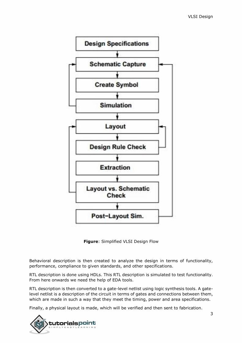
VLSI Design Flow
The VLSI IC circuits design flow is shown in the figure below. The various levels of design
are numbered and the blocks show processes in the design flow.
Specifications comes first, they describe abstractly, the functionality, interface, and the
architecture of the digital IC circuit to be designed.
1. VLSI – Digital System
VLSI Design
3
Figure: Simplified VLSI Design Flow
Behavioral description is then created to analyze the design in terms of functionality,
performance, compliance to given standards, and other specifications.
RTL description is done using HDLs. This RTL description is simulated to test functionality.
From here onwards we need the help of EDA tools.
RTL description is then converted to a gate-level netlist using logic synthesis tools. A gate-
level netlist is a description of the circuit in terms of gates and connections between them,
which are made in such a way that they meet the timing, power and area specifications.
Finally, a physical layout is made, which will be verified and then sent to fabrication.
VLSI Design
4
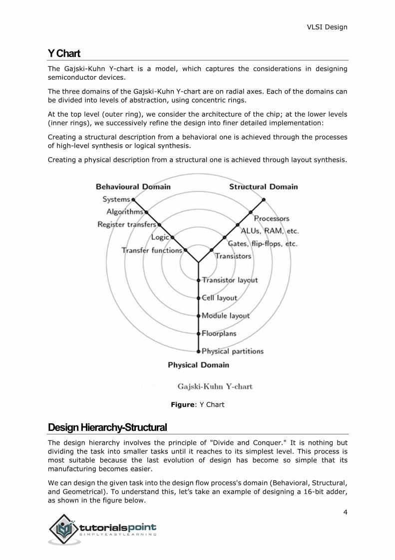
Y Chart
The Gajski-Kuhn Y-chart is a model, which captures the considerations in designing
semiconductor devices.
The three domains of the Gajski-Kuhn Y-chart are on radial axes. Each of the domains can
be divided into levels of abstraction, using concentric rings.
At the top level (outer ring), we consider the architecture of the chip; at the lower levels
(inner rings), we successively refine the design into finer detailed implementation:
Creating a structural description from a behavioral one is achieved through the processes
of high-level synthesis or logical synthesis.
Creating a physical description from a structural one is achieved through layout synthesis.
Figure: Y Chart
Design Hierarchy-Structural
The design hierarchy involves the principle of "Divide and Conquer." It is nothing but
dividing the task into smaller tasks until it reaches to its simplest level. This process is
most suitable because the last evolution of design has become so simple that its
manufacturing becomes easier.
We can design the given task into the design flow process's domain (Behavioral, Structural,
and Geometrical). To understand this, let’s take an example of designing a 16-bit adder,
as shown in the figure below.
VLSI Design
5
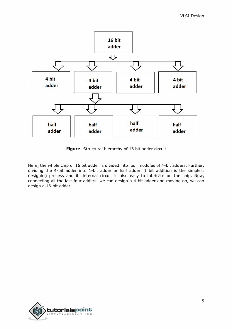
Figure: Structural hierarchy of 16 bit adder circuit
Here, the whole chip of 16 bit adder is divided into four modules of 4-bit adders. Further,
dividing the 4-bit adder into 1-bit adder or half adder. 1 bit addition is the simplest
designing process and its internal circuit is also easy to fabricate on the chip. Now,
connecting all the last four adders, we can design a 4-bit adder and moving on, we can
design a 16-bit adder.

VLSI Design
6
Figure: Decomposition of a 4 bit adder
VLSI Design
7
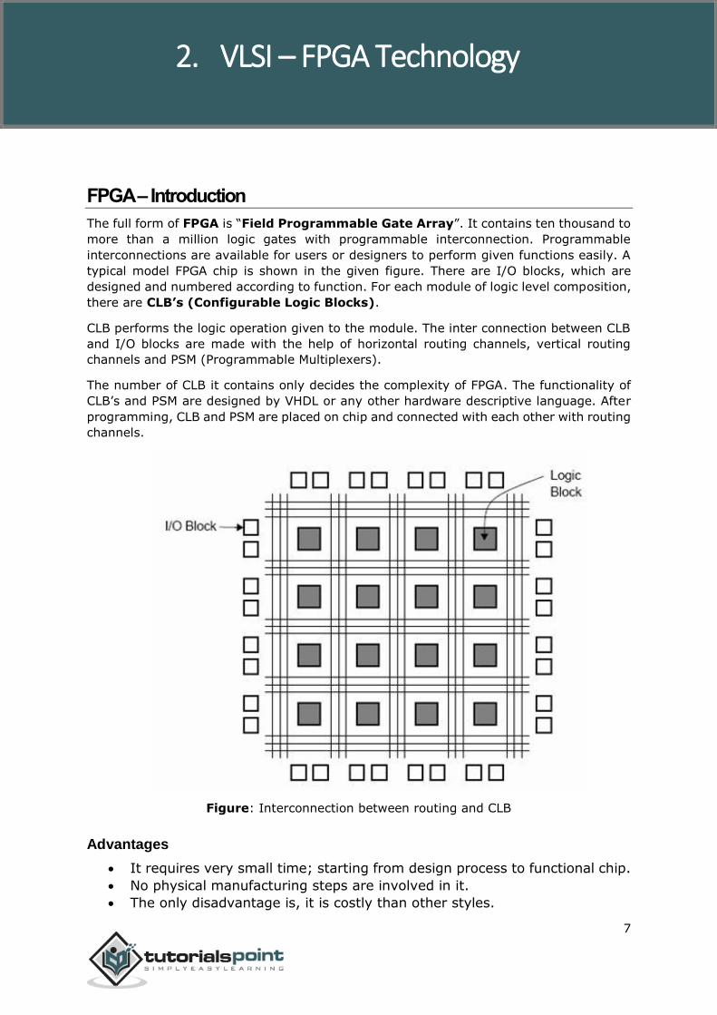
FPGA – Introduction
The full form of FPGA is “Field Programmable Gate Array”. It contains ten thousand to
more than a million logic gates with programmable interconnection. Programmable
interconnections are available for users or designers to perform given functions easily. A
typical model FPGA chip is shown in the given figure. There are I/O blocks, which are
designed and numbered according to function. For each module of logic level composition,
there are CLB’s (Configurable Logic Blocks).
CLB performs the logic operation given to the module. The inter connection between CLB
and I/O blocks are made with the help of horizontal routing channels, vertical routing
channels and PSM (Programmable Multiplexers).
The number of CLB it contains only decides the complexity of FPGA. The functionality of
CLB’s and PSM are designed by VHDL or any other hardware descriptive language. After
programming, CLB and PSM are placed on chip and connected with each other with routing
channels.
Figure: Interconnection between routing and CLB
Advantages
It requires very small time; starting from design process to functional chip.
No physical manufacturing steps are involved in it.
The only disadvantage is, it is costly than other styles.
2. VLSI – FPGA Technology

VLSI Design
8
Gate Array Design
The gate array (GA) ranks second after the FPGA, in terms of fast prototyping capability.
While user programming is important to the design implementation of the FPGA chip, metal
mask design and processing is used for GA. Gate array implementation requires a two-
step manufacturing process.
The first phase results in an array of uncommitted transistors on each GA chip. These
uncommitted chips can be stored for later customization, which is completed by defining
the metal interconnects between the transistors of the array. The patterning of metallic
interconnects is done at the end of the chip fabrication process, so that the turn-around
time can still be short, a few days to a few weeks. The figure given below shows the basic
processing steps for gate array implementation.
Figure: Basic Processing Steps for gate array implementation
Typical gate array platforms use dedicated areas called channels, for inter-cell routing
between rows or columns of MOS transistors. They simplify the interconnections.
Interconnection patterns that perform basic logic gates are stored in a library, which can
then be used to customize rows of uncommitted transistors according to the netlist.
In most of the modern GAs, multiple metal layers are used for channel routing. With the
use of multiple interconnected layers, the routing can be achieved over the active cell
areas; so that the routing channels can be removed as in Sea-of-Gates (SOG) chips. Here,
the entire chip surface is covered with uncommitted nMOS and pMOS transistors. The
neighboring transistors can be customized using a metal mask to form basic logic gates.
For inter cell routing, some of the uncommitted transistors must be sacrificed. This design
style results in more flexibility for interconnections and usually in a higher density. GA chip
utilization factor is measured by the used chip area divided by the total chip area. It is
higher than that of the FPGA and so is the chip speed.

VLSI Design
9
Standard Cell Based Design
A standard cell based design requires development of a full custom mask set. The standard
cell is also known as the polycell. In this approach, all of the commonly used logic cells
are developed, characterized and stored in a standard cell library.
A library may contain a few hundred cells including inverters, NAND gates, NOR gates,
complex AOI, OAI gates, D-latches and Flip-flops. Each gate type can be implemented in
several versions to provide adequate driving capability for different fan-outs. The inverter
gate can have standard size, double size, and quadruple size so that the chip designer can
select the proper size to obtain high circuit speed and layout density.
Each cell is characterized according to several different characterization categories, such
as,
Delay time versus load capacitance
Circuit simulation model
Timing simulation model
Fault simulation model
Cell data for place-and-route
Mask data
For automated placement of the cells and routing, each cell layout is designed with a fixed
height, so that a number of cells can be bounded side-by-side to form rows. The power
and ground rails run parallel to the upper and lower boundaries of the cell. So that,
neighboring cells share a common power bus and a common ground bus. The figure shown
below is a floorplan for standard-cell based design.
Figure: Floor Plan for Standard Cell Based Design

VLSI Design
10
Full Custom Design
In a full-custom design, the entire mask design is made new, without the use of any
library. The development cost of this design style is rising. Thus, the concept of design
reuse is becoming famous to reduce design cycle time and development cost.
The hardest full custom design can be the design of a memory cell, be it static or dynamic.
For logic chip design, a good negotiation can be obtained using a combination of different
design styles on the same chip, i.e. standard cells, data-path cells, and programmable
logic arrays (PLAs).
Practically, the designer does the full custom layout, i.e. the geometry, orientation, and
placement of every transistor. The design productivity is usually very low; typically a few
tens of transistors per day, per designer. In digital CMOS VLSI, full-custom design is hardly
used due to the high labor cost. These design styles include the design of high-volume
products such as memory chips, high-performance microprocessors and FPGA.
VLSI Design
11
Complementary MOSFET (CMOS) technology is widely used today to form circuits in
numerous and varied applications. Today’s computers, CPUs and cell phones make use of
CMOS due to several key advantages. CMOS offers low power dissipation, relatively high
speed, high noise margins in both states, and will operate over a wide range of source and
input voltages (provided the source voltage is fixed)
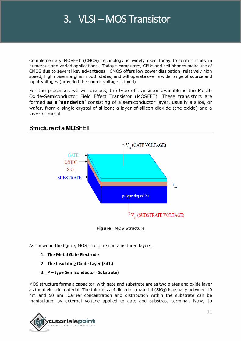
For the processes we will discuss, the type of transistor available is the Metal-
Oxide-Semiconductor Field Effect Transistor (MOSFET). These transistors are
formed as a ‘sandwich’ consisting of a semiconductor layer, usually a slice, or
wafer, from a single crystal of silicon; a layer of silicon dioxide (the oxide) and a
layer of metal.
Structure of a MOSFET
Figure: MOS Structure
As shown in the figure, MOS structure contains three layers:
1. The Metal Gate Electrode
2. The Insulating Oxide Layer (SiO2)
3. P – type Semiconductor (Substrate)
MOS structure forms a capacitor, with gate and substrate are as two plates and oxide layer
as the dielectric material. The thickness of dielectric material (SiO2) is usually between 10
nm and 50 nm. Carrier concentration and distribution within the substrate can be
manipulated by external voltage applied to gate and substrate terminal. Now, to
3. VLSI – MOS Transistor
VLSI Design
12
understand the structure of MOS, first consider the basic electric properties of P –
Type semiconductor substrate.
Concentration of carrier in semiconductor material is always following the Mass Action
Law. Mass Action Law is given by:
n . p = ni2
Where,
n is carrier concentration of electrons
p is carrier concentration of holes
ni is intrinsic carrier concentration of Silicon
Now assume that substrate is equally doped with acceptor (Boron) concentration NA. So,
electron and hole concentration in p–type substrate is
npo =ni
2
NA
ppo = NA
Here, doping concentration NA is (1015 to 1016 cm-3) greater than intrinsic concentration
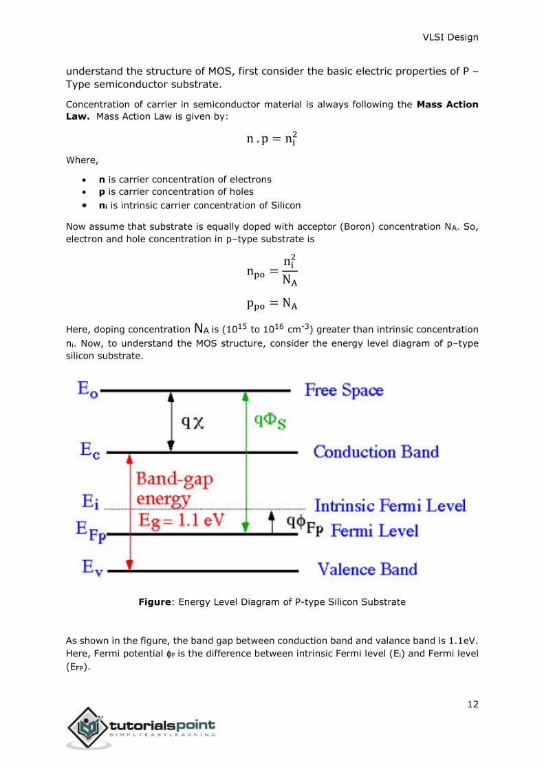
ni. Now, to understand the MOS structure, consider the energy level diagram of p–type
silicon substrate.
Figure: Energy Level Diagram of P-type Silicon Substrate
As shown in the figure, the band gap between conduction band and valance band is 1.1eV.
Here, Fermi potential ɸF is the difference between intrinsic Fermi level (Ei) and Fermi level
(EFP).
VLSI Design
13
Where Fermi level EF depends on the doping concentration. Fermi potential ɸF is the
difference between intrinsic Fermi level (Ei) and Fermi level (EFP).
Mathematically,
ϕFp =EF − Ei
q
The potential difference between conduction band and free space is called electron affinity
and is denoted by qx.
So, energy required for an electron to move from Fermi level to free space is called work
function (qϕS) and it is given by
qϕS = (Ec − EF) + qx
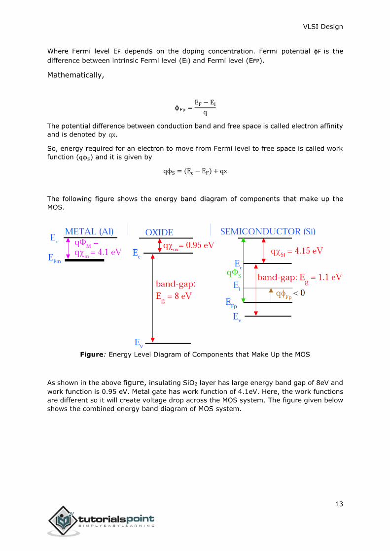
The following figure shows the energy band diagram of components that make up the
MOS.
Figure: Energy Level Diagram of Components that Make Up the MOS
As shown in the above figure, insulating SiO2 layer has large energy band gap of 8eV and
work function is 0.95 eV. Metal gate has work function of 4.1eV. Here, the work functions
are different so it will create voltage drop across the MOS system. The figure given below
shows the combined energy band diagram of MOS system.
VLSI Design
14
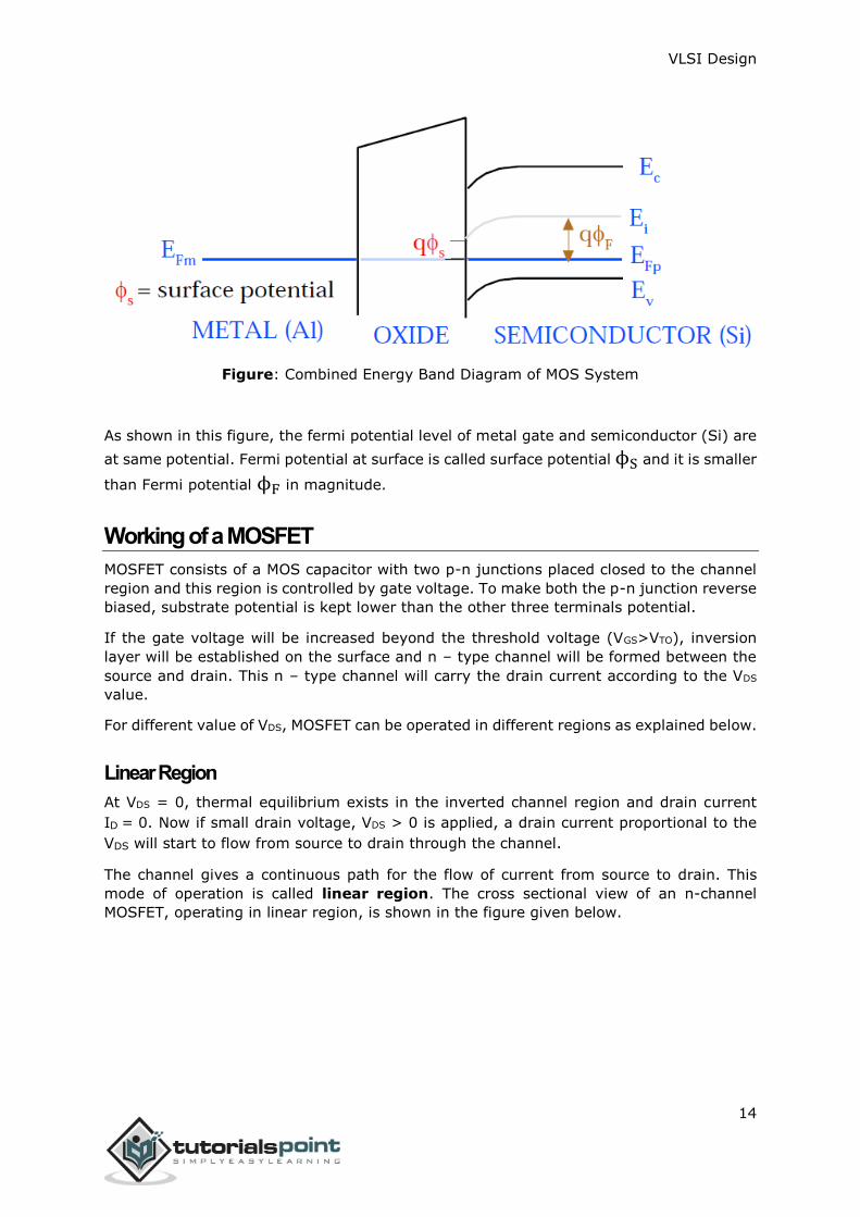
Figure: Combined Energy Band Diagram of MOS System
As shown in this figure, the fermi potential level of metal gate and semiconductor (Si) are
at same potential. Fermi potential at surface is called surface potential ϕS and it is smaller
than Fermi potential ϕF in magnitude.
Working of a MOSFET
MOSFET consists of a MOS capacitor with two p-n junctions placed closed to the channel
region and this region is controlled by gate voltage. To make both the p-n junction reverse
biased, substrate potential is kept lower than the other three terminals potential.
If the gate voltage will be increased beyond the threshold voltage (VGS>VTO), inversion
layer will be established on the surface and n – type channel will be formed between the
source and drain. This n – type channel will carry the drain current according to the VDS
value.
For different value of VDS, MOSFET can be operated in different regions as explained below.
Linear Region
At VDS = 0, thermal equilibrium exists in the inverted channel region and drain current
ID = 0. Now if small drain voltage, VDS > 0 is applied, a drain current proportional to the
VDS will start to flow from source to drain through the channel.
The channel gives a continuous path for the flow of current from source to drain. This
mode of operation is called linear region. The cross sectional view of an n-channel
MOSFET, operating in linear region, is shown in the figure given below.

VLSI Design
15
Figure: MOSFET in Linear Region
At the Edge of Saturation Region
Now if the VDS is increased, charges in the channel and channel depth decrease at the end
of drain. For VDS = VDSAT, the charges in the channel is reduces to zero, which is called
pinch – off point. The cross sectional view of n-channel MOSFET operating at the edge
of saturation region is shown in the figure given below.
Figure: MOSFET at the Edge of Saturation Region
Saturation Region
For VDS>VDSAT, a depleted surface forms near to drain, and by increasing the drain voltage
this depleted region extends to source.
This mode of operation is called Saturation region. The electrons coming from the source
to the channel end, enter in the drain – depletion region and are accelerated towards the
drain in high electric field.

VLSI Design
16
Figure: MOSFET in Saturation Region
MOSFET Current – Voltage Characteristics
To understand the current – voltage characteristic of MOSFET, approximation for the
channel is done. Without this approximation, the three dimension analysis of MOS system
becomes complex. The Gradual Channel Approximation (GCA) for current – voltage
characteristic will reduce the analysis problem.
Gradual Channel Approximation (GCA)
Consider the cross sectional view of n channel MOSFET operating in the linear mode. Here,
source and substrate are connected to the ground. VS = VB = 0. The gate – to – source
(VGS) and drain – to – source voltage (VDS) voltage are the external parameters that control
the drain current ID.
Figure: Gradual Channel Approximation
VLSI Design
17
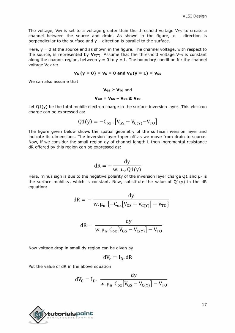
The voltage, VGS is set to a voltage greater than the threshold voltage VTO, to create a
channel between the source and drain. As shown in the figure, x – direction is
perpendicular to the surface and y – direction is parallel to the surface.
Here, y = 0 at the source end as shown in the figure. The channel voltage, with respect to
the source, is represented by VC(Y). Assume that the threshold voltage VTO is constant
along the channel region, between y = 0 to y = L. The boundary condition for the channel
voltage VC are:
VC (y = 0) = VS = 0 and VC (y = L) = VDS
We can also assume that
VGS ≥ VTO and
VGD = VGS – VDS ≥ VTO
Let Q1(y) be the total mobile electron charge in the surface inversion layer. This electron
charge can be expressed as:
Q1(y) = −Cox . [VGS − VC(Y)−VTO]
The figure given below shows the spatial geometry of the surface inversion layer and
indicate its dimensions. The inversion layer taper off as we move from drain to source.
Now, if we consider the small region dy of channel length L then incremental resistance
dR offered by this region can be expressed as:
dR = −dy
w. μn. Q1(y)
Here, minus sign is due to the negative polarity of the inversion layer charge Q1 and μn is
the surface mobility, which is constant. Now, substitute the value of Q1(y) in the dR
equation:
dR = − dy
w. μn. {−Cox[VGS − VC(Y)] − VTO}
dR = dy
w. μn. Cox[VGS − VC(Y)] − VTO
Now voltage drop in small dy region can be given by
dVc = ID. dR
Put the value of dR in the above equation
dVC = ID . dy
𝑤. μn. Cox[VGS − VC(Y)] − VTO
VLSI Design
18
w. μn. Cox[VGS − VC(Y) − VTO]. dVC = ID. dy
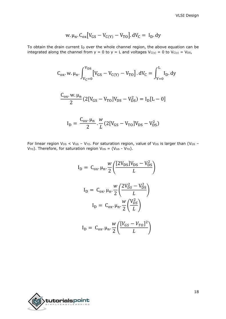
To obtain the drain current ID over the whole channel region, the above equation can be
integrated along the channel from y = 0 to y = L and voltages VC(y) = 0 to VC(y) = VDS,
Cox. w. μn. ∫ [VGS − VC(Y) − VTO]VDS
VC=0
. dVC = ∫ ID. dyL
Y=0
Cox. w. μn
2(2[VGS − VTO]VDS − VDS
2 ) = ID[L − 0]
ID = Cox. μn
2.𝑤
𝐿(2[VGS − VTO]VDS − VDS
2 )
For linear region VDS < VGS – VTO. For saturation region, value of VDS is larger than (VGS –
VTO). Therefore, for saturation region VDS = (VGS - VTO).
ID = Cox. μn.𝑤
2(
[2VDS]VDS − VDS2
𝐿)
ID = Cox. μn.𝑤
2(
2V𝐷𝑆2 − VDS
2
𝐿)
ID = Cox. μn.𝑤
2(
V𝐷𝑆2
𝐿)
ID = Cox. μn.𝑤
2(
[𝑉𝐺𝑆 − 𝑉𝑇𝑂]2
𝐿)

VLSI Design
19
The inverter is truly the nucleus of all digital designs. Once its operation and properties
are clearly understood, designing more intricate structures such as NAND gates, adders,
multipliers, and microprocessors is greatly simplified. The electrical behavior of these
complex circuits can be almost completely derived by extrapolating the results obtained
for inverters.
The analysis of inverters can be extended to explain the behavior of more complex gates
such as NAND, NOR, or XOR, which in turn form the building blocks for modules such as
multipliers and processors. In this chapter, we focus on one single incarnation of the
inverter gate, being the static CMOS inverter — or the CMOS inverter, in short. This is
certainly the most popular at present and therefore deserves our special attention.
Principle of Operation
The logic symbol and truth table of ideal inverter is shown in figure given below. Here A is
the input and B is the inverted output represented by their node voltages. Using positive
logic, the Boolean value of logic 1 is represented by Vdd and logic 0 is represented by 0.
Vth is the inverter threshold voltage, which is Vdd /2, where Vdd is the output voltage.
The output is switched from 0 to Vdd when input is less than Vth. So, for 0<Vin<Vth output
is equal to logic 0 input and Vth<Vin< Vdd is equal to logic 1 input for inverter.
Figure: Logical Symbol and Truth Table of inverter
4. VLSI – MOS Inverter
VLSI Design
20
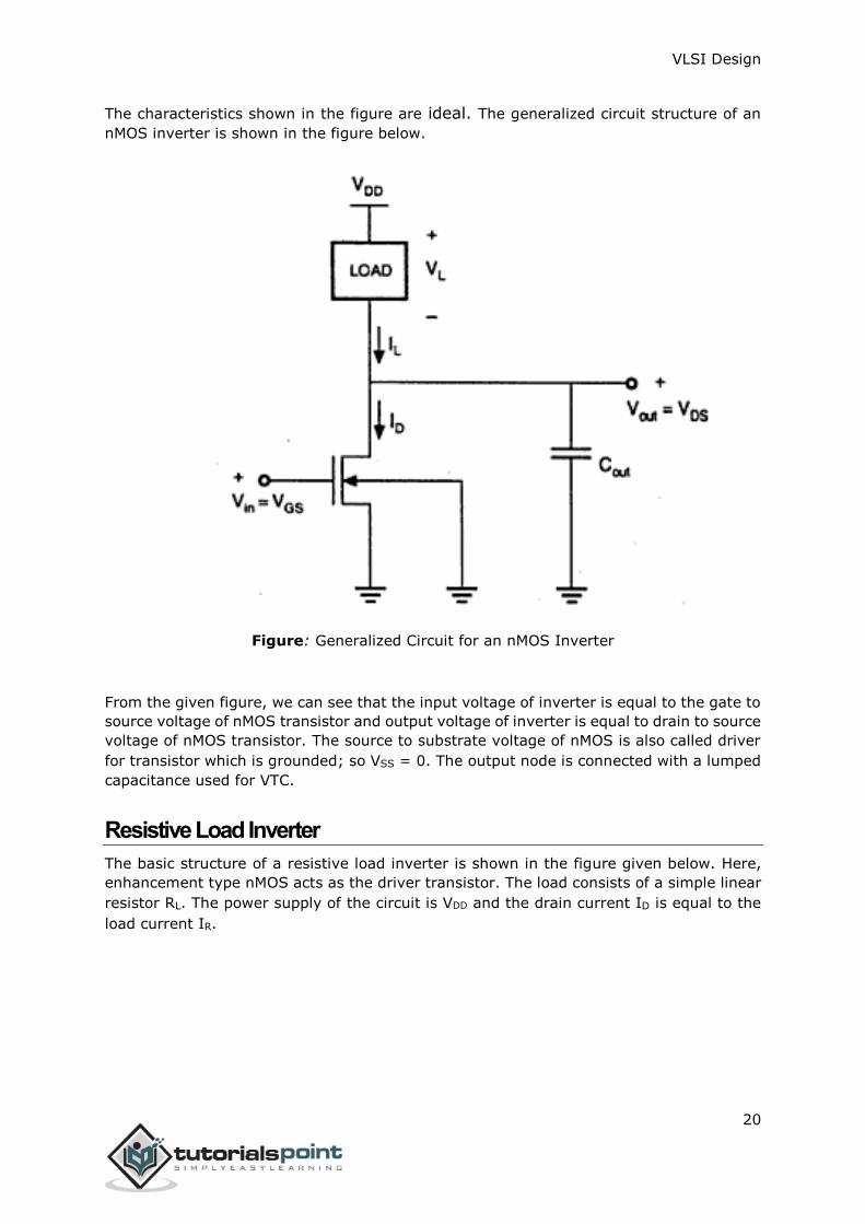
The characteristics shown in the figure are ideal. The generalized circuit structure of an
nMOS inverter is shown in the figure below.
Figure: Generalized Circuit for an nMOS Inverter
From the given figure, we can see that the input voltage of inverter is equal to the gate to
source voltage of nMOS transistor and output voltage of inverter is equal to drain to source
voltage of nMOS transistor. The source to substrate voltage of nMOS is also called driver
for transistor which is grounded; so VSS = 0. The output node is connected with a lumped
capacitance used for VTC.
Resistive Load Inverter
The basic structure of a resistive load inverter is shown in the figure given below. Here,
enhancement type nMOS acts as the driver transistor. The load consists of a simple linear
resistor RL. The power supply of the circuit is VDD and the drain current ID is equal to the
load current IR.

VLSI Design
21
Figure: Resistive Load nMOS Inverter Circuit
Circuit Operation
When the input of the driver transistor is less than threshold voltage VTH (Vin < VTH), driver
transistor is in the cut – off region and does not conduct any current. So, the voltage drop
across the load resistor is ZERO and output voltage is equal to the VDD. Now, when the
input voltage increases further, driver transistor will start conducting the non-zero current
and nMOS goes in saturation region.
Mathematically,
ID =Kn
2[VGS − VTO]2
Increasing the input voltage further, driver transistor will enter into the linear region and
output of the driver transistor decreases.
ID =Kn
2 2[VGS − VTO]VDS − VDS
2
VTC of the resistive load inverter, shown below, indicates the operating mode of driver
transistor and voltage points.

VLSI Design
22
Figure: Voltage Transfer Characteristic of Resistive Load Inverter
Inverter with N type MOSFET Load
The main advantage of using MOSFET as load device is that the silicon area occupied by
the transistor is smaller than the area occupied by the resistive load. Here, MOSFET is
active load and inverter with active load gives a better performance than the inverter with
resistive load.
Enhancement Load NMOS
Two inverters with enhancement-type load device are shown in the figure. Load transistor
can be operated either, in saturation region or in linear region, depending on the bias
voltage applied to its gate terminal. The saturated enhancement load inverter is shown in
the fig. (a). It requires a single voltage supply and simple fabrication process and so VOH
is limited to the VDD – VT.
(a) (b)
Figure: (a) Saturated Enhancement type nMOS type Load
(b) Linear Enhancement type nMOS type Load
VLSI Design
23
The linear enhancement load inverter is shown in the fig. (b). It always operates in linear
region; so VOH level is equal to VDD.
Linear load inverter has higher noise margin compared to the saturated enhancement
inverter. But, the disadvantage of linear enhancement inverter is, it requires two separate
power supply and both the circuits suffer from high power dissipation. Therefore,
enhancement inverters are not used in any large-scale digital applications.
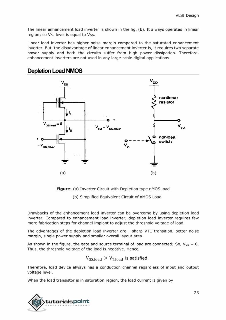
Depletion Load NMOS
(a) (b)
Figure: (a) Inverter Circuit with Depletion type nMOS load
(b) Simplified Equivalent Circuit of nMOS Load
Drawbacks of the enhancement load inverter can be overcome by using depletion load
inverter. Compared to enhancement load inverter, depletion load inverter requires few
more fabrication steps for channel implant to adjust the threshold voltage of load.
The advantages of the depletion load inverter are - sharp VTC transition, better noise
margin, single power supply and smaller overall layout area.
As shown in the figure, the gate and source terminal of load are connected; So, VGS = 0.
Thus, the threshold voltage of the load is negative. Hence,
VGS,load > VT,load is satisfied
Therefore, load device always has a conduction channel regardless of input and output
voltage level.
When the load transistor is in saturation region, the load current is given by

VLSI Design
24
ID,load =kn,load
2[−VT,load (Vout)]
2
When the load transistor is in linear region, the load current is given by
ID,load =kn,load
2[2|VT,load(Vout)| . (VDD − Vout) − (VDD − Vout)2]
The voltage transfer characteristics of the depletion load inverter is shown in the figure
given below.
Figure: Typical VTC of Depletion Load nMOS Inverter
CMOS Inverter – Circuit, Operation and Description
The CMOS inverter circuit is shown in the figure. Here, nMOS and pMOS transistors work
as driver transistors; when one transistor is ON, other is OFF.

VLSI Design
25
Figure: CMOS Inverter Circuit
This configuration is called complementary MOS (CMOS). The input is connected to the
gate terminal of both the transistors such that both can be driven directly with input
voltages. Substrate of the nMOS is connected to the ground and substrate of the pMOS is
connected to the power supply, VDD.
So VSB = 0 for both the transistors.
VGS,n = Vin
VDS,n = Vout And,
VGS,p = Vin − 𝑉𝐷𝐷
VDS,p = Vout − VDD
When the input of nMOS is smaller than the threshold voltage (Vin < VTO,n), the nMOS is
cut – off and pMOS is in linear region. So, the drain current of both the transistors is zero.
ID,n = ID,p = 0
Therefore, the output voltage VOH is equal to the supply voltage.
Vout = VOH = VDD

VLSI Design
26
When the input voltage is greater than the VDD + VTO,p, the pMOS transistor is in the cut-
off region and the nMOS is in the linear region, so the drain current of both the transistors
is zero.
ID, n = ID, p = 0
Therefore, the output voltage VOL is equal to zero.
Vout = VOL = 0
The nMOS operates in the saturation region if Vin > VTO and if following conditions are
satisfied.
VDS, n ≥ VGS, n – VTO, n
Vout ≥ Vin – VTO, n
The pMOS operates in the saturation region if Vin < VDD + VTO,p and if following conditions
are satisfied.
VDS, p ≤ VGS, p – VTO, p
Vout ≤ Vin – VTO, p
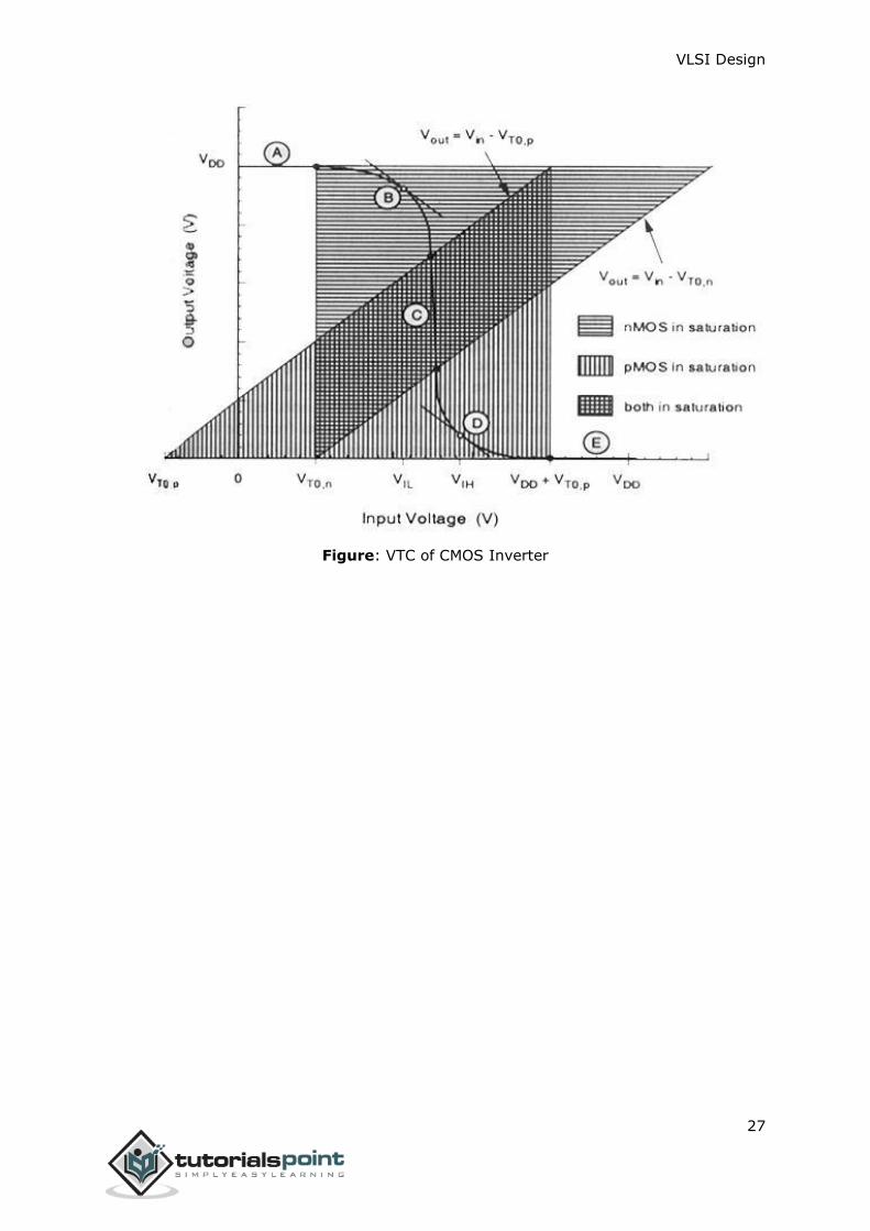
For different value of input voltages, the operating regions are listed below for both
transistors.
Region Vin Vout nMOS pMOS
A < VTO, n VOH Cut – off Linear
B VIL High ≈ VOH Saturation Linear
C Vth Vth Saturation Saturation
D VIH Low ≈ VOL Linear Saturation
E > (VDD + VTO, p) VOL Linear Cut – off
The VTC of CMOS is shown in the figure below:
VLSI Design
27
Figure: VTC of CMOS Inverter

VLSI Design
28
Combinational logic circuits or gates, which perform Boolean operations on multiple input
variables and determine the outputs as Boolean functions of the inputs, are the basic
building blocks of all digital systems. We will examine simple circuit configurations such as
two-input NAND and NOR gates and then expand our analysis to more general cases of
multiple-input circuit structures.
Next, the CMOS logic circuits will be presented in a similar fashion. We will stress the
similarities and differences between the nMOS depletion-load logic and CMOS logic circuits
and point out the advantages of CMOS gates with examples. In its most general form, a
combinational logic circuit, or gate, performing a Boolean function can be represented as
a multiple-input, single-output system, as depicted in the figure.
Figure: Combinational Logic Circuit
Node voltages, referenced to the ground potential, represent all input variables. Using
positive logic convention, the Boolean (or logic) value of "1" can be represented by a high
voltage of VDD, and the Boolean (or logic) value of "0" can be represented by a low voltage
of 0. The output node is loaded with a capacitance CL, which represents the combined
capacitances of the parasitic device in the circuit.
CMOS Logic Circuits
CMOS Two input NOR Gate
The circuit consists of a parallel-connected n-net and a series-connected complementary
p-net. The input voltages VX and VY are applied to the gates of one nMOS and one pMOS
transistor.
5. VLSI – Combinational MOS Logic Circuits
VLSI Design
29
When either one or both inputs are high, i.e., when the n-net creates a conducting path
between the output node and the ground, the p-net is cut—off. If both input voltages are
low, i.e., the n-net is cut-off, then the p-net creates a conducting path between the output
node and the supply voltage.
For any given input combination, the complementary circuit structure is such that the
output is connected either to VDD or to ground via a low-resistance path and a DC current
path between the VDD and ground is not established for any input combinations. The output
voltage of the CMOS, two input NOR gate will get a logic-low voltage of VOL = 0 and a
logic-high voltage of VOH = VDD. The equation of the switching threshold voltage Vth is
given by
𝑉𝑡ℎ(𝑁𝑂𝑅2) =
𝑉𝑇,𝑛 +12
√𝑘𝑝
𝑘𝑛(𝑉𝐷𝐷 − |𝑉𝑇,𝑝|)
1 +12
√𝑘𝑝
𝑘𝑛
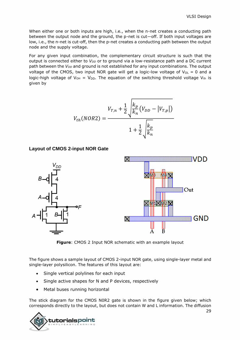
Layout of CMOS 2-input NOR Gate
Figure: CMOS 2 Input NOR schematic with an example layout
The figure shows a sample layout of CMOS 2-input NOR gate, using single-layer metal and
single-layer polysilicon. The features of this layout are:
Single vertical polylines for each input
Single active shapes for N and P devices, respectively
Metal buses running horizontal
The stick diagram for the CMOS N0R2 gate is shown in the figure given below; which
corresponds directly to the layout, but does not contain W and L information. The diffusion
VLSI Design
30
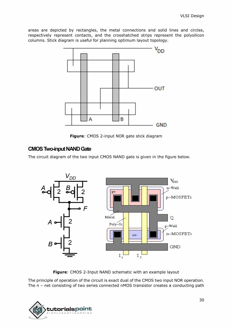
areas are depicted by rectangles, the metal connections and solid lines and circles,
respectively represent contacts, and the crosshatched strips represent the polysilicon
columns. Stick diagram is useful for planning optimum layout topology.
Figure: CMOS 2-input NOR gate stick diagram
CMOS Two-input NAND Gate
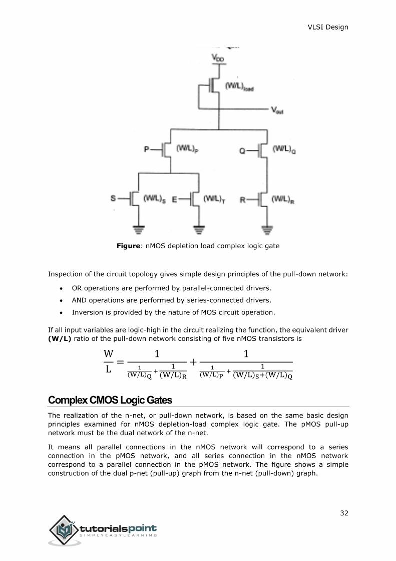
The circuit diagram of the two input CMOS NAND gate is given in the figure below.
Figure: CMOS 2-Input NAND schematic with an example layout
The principle of operation of the circuit is exact dual of the CMOS two input NOR operation.
The n – net consisting of two series connected nMOS transistor creates a conducting path

VLSI Design
31
between the output node and the ground, if both input voltages are logic high. Both of the
parallelly connected pMOS transistor in p-net will be off.
For all other input combination, either one or both of the pMOS transistor will be turn ON,
while p – net is cut off, thus, creating a current path between the output node and the
power supply voltage. The switching threshold for this gate is obtained as -
𝑉𝑡ℎ(𝑁𝐴𝑁𝐷2) =
𝑉𝑇,𝑛 + 2√𝑘𝑝
𝑘𝑛(𝑉𝐷𝐷 − |𝑉𝑇,𝑝|)
1 + 2√𝑘𝑝
𝑘𝑛
The features of this layout are as follows:
Single polysilicon lines for inputs run vertically across both N and P active regions.
Single active shapes are used for building both nMOS devices and both pMOS
devices.
Power bussing is running horizontal across top and bottom of layout.
Output wires runs horizontal for easy connection to neighboring circuit.
Complex Logic Circuits
NMOS Depletion Load Complex Logic Gate
To realize complex functions of multiple input variables, the basic circuit structures and
design principles developed for NOR and NAND can be extended to complex logic gates.
The ability to realize complex logic functions, using a small number of transistors is one of
the most attractive features of nMOS and CMOS logic circuits. Consider the following
Boolean function as an example.
𝐙 = 𝐏(𝐒 + 𝐓) + 𝐐𝐑̅̅ ̅̅ ̅̅ ̅̅ ̅̅ ̅̅ ̅̅ ̅̅ ̅̅ ̅̅ ̅̅ ̅̅ ̅
The nMOS depletion-load complex logic gate used to realize this function is shown in figure.
In this figure, the left nMOS driver branch of three driver transistors is used to perform
the logic function P (S + T), while the right-hand side branch performs the function QR.
By connecting the two branches in parallel, and by placing the load transistor between the
output node and the supply voltage VDD, we obtain the given complex function. Each input
variable is assigned to only one driver.
VLSI Design
32
Figure: nMOS depletion load complex logic gate
Inspection of the circuit topology gives simple design principles of the pull-down network:
OR operations are performed by parallel-connected drivers.
AND operations are performed by series-connected drivers.
Inversion is provided by the nature of MOS circuit operation.
If all input variables are logic-high in the circuit realizing the function, the equivalent driver
(W/L) ratio of the pull-down network consisting of five nMOS transistors is
W
L=
11
(W/L)Q +
1(W/L)R
+1
1(W/L)P
+ 1
(W/L)S+(W/L)Q
Complex CMOS Logic Gates
The realization of the n-net, or pull-down network, is based on the same basic design
principles examined for nMOS depletion-load complex logic gate. The pMOS pull-up
network must be the dual network of the n-net.
It means all parallel connections in the nMOS network will correspond to a series
connection in the pMOS network, and all series connection in the nMOS network
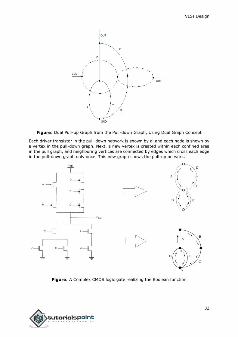
correspond to a parallel connection in the pMOS network. The figure shows a simple
construction of the dual p-net (pull-up) graph from the n-net (pull-down) graph.
VLSI Design
33
Figure: Dual Pull-up Graph from the Pull-down Graph, Using Dual Graph Concept
Each driver transistor in the pull-down network is shown by ai and each node is shown by
a vertex in the pull-down graph. Next, a new vertex is created within each confined area
in the pull graph, and neighboring vertices are connected by edges which cross each edge
in the pull-down graph only once. This new graph shows the pull-up network.
Figure: A Complex CMOS logic gate realizing the Boolean function

VLSI Design
34
Layout Technique using Euler Graph Method
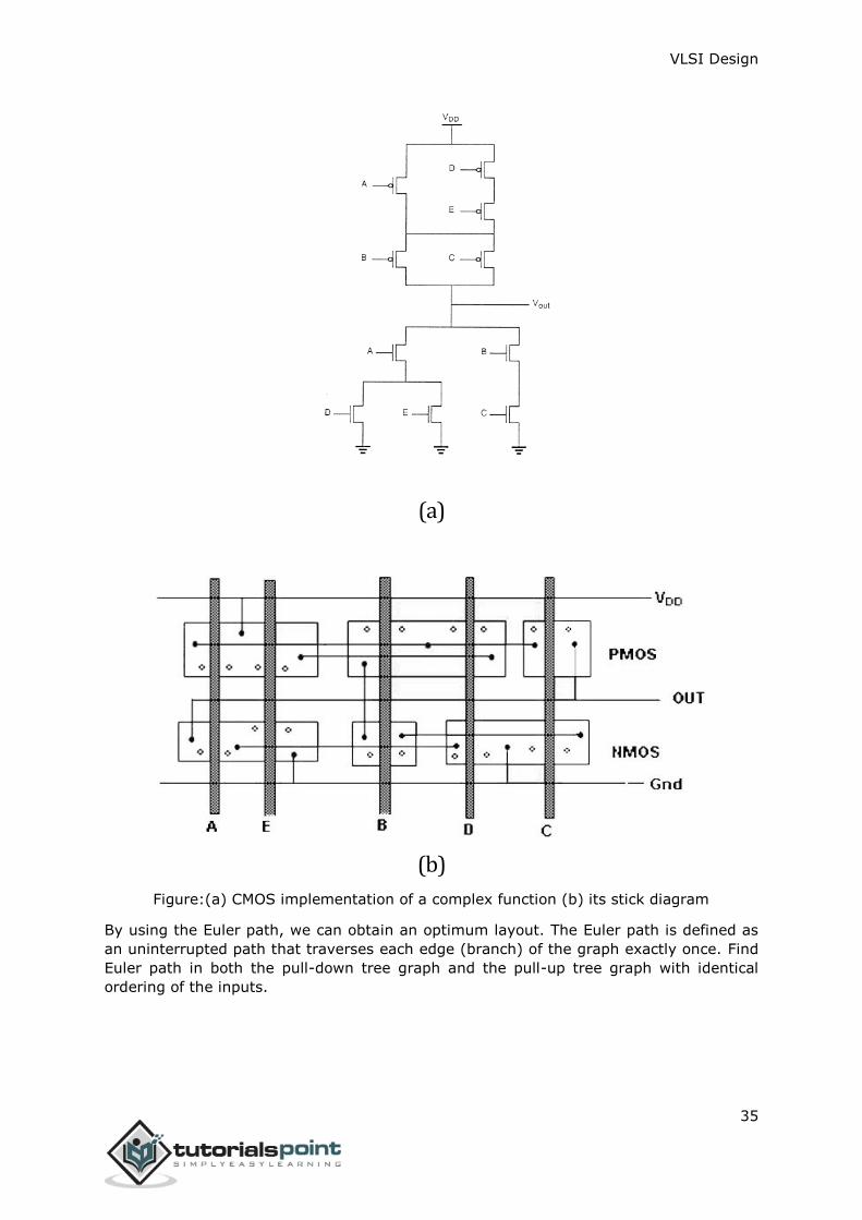
The figure shows the CMOS implementation of a complex function and its stick diagram
done with arbitrary gate ordering that gives a very non-optimum layout for the CMOS
gate.
In this case, the separation between the polysilicon columns must allow diffusion-to-
diffusion separation in between. This certainly consumes a considerably amount of extra
silicon area.
VLSI Design
35
(a)
(b)
Figure:(a) CMOS implementation of a complex function (b) its stick diagram
By using the Euler path, we can obtain an optimum layout. The Euler path is defined as
an uninterrupted path that traverses each edge (branch) of the graph exactly once. Find
Euler path in both the pull-down tree graph and the pull-up tree graph with identical
ordering of the inputs.
VLSI Design
36
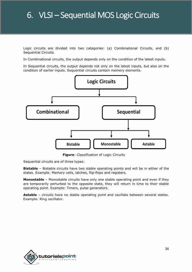
Logic circuits are divided into two categories: (a) Combinational Circuits, and (b)
Sequential Circuits.
In Combinational circuits, the output depends only on the condition of the latest inputs.
In Sequential circuits, the output depends not only on the latest inputs, but also on the
condition of earlier inputs. Sequential circuits contain memory elements.
Figure: Classification of Logic Circuits
Sequential circuits are of three types:
Bistable – Bistable circuits have two stable operating points and will be in either of the
states. Example: Memory cells, latches, flip-flops and registers.
Monostable – Monostable circuits have only one stable operating point and even if they
are temporarily perturbed to the opposite state, they will return in time to their stable
operating point. Example: Timers, pulse generators.
Astable – circuits have no stable operating point and oscillate between several states.
Example: Ring oscillator.
6. VLSI – Sequential MOS Logic Circuits

VLSI Design
37
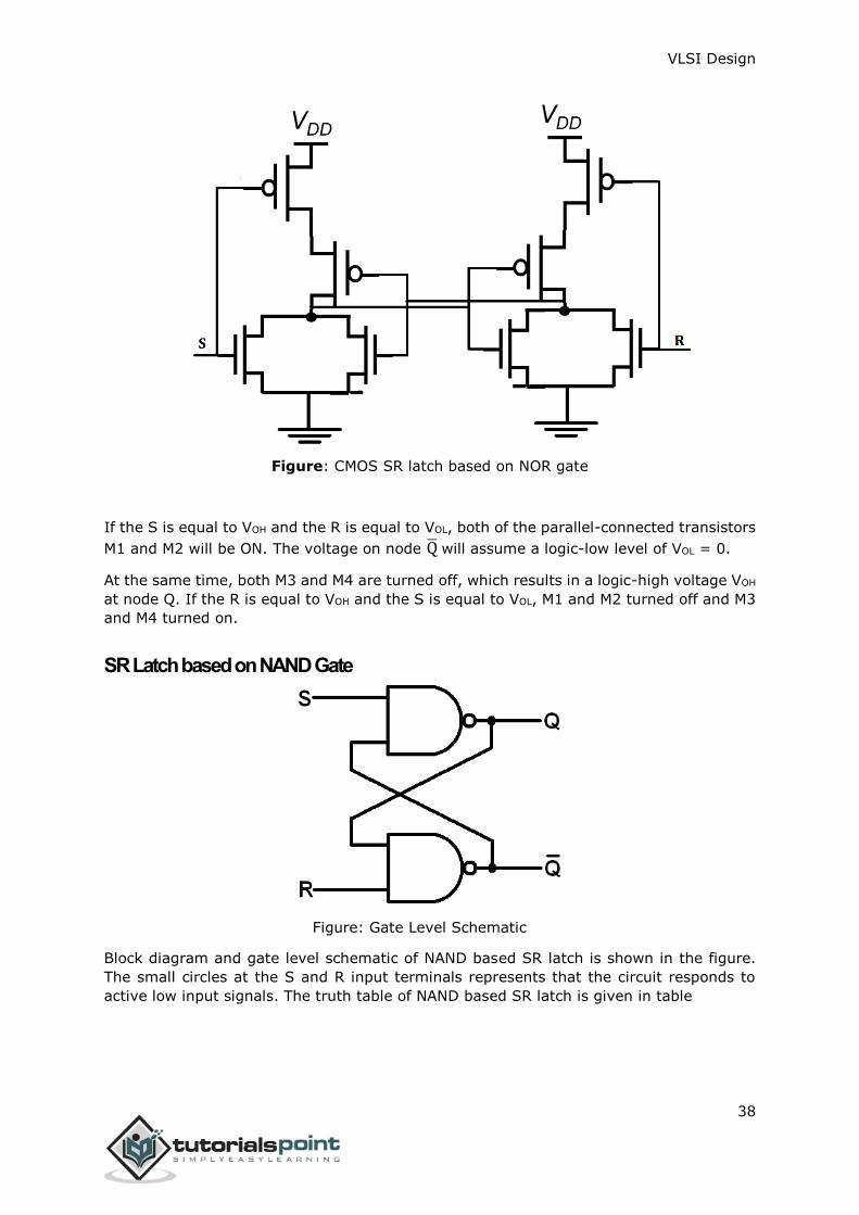
CMOS Logic Circuits
SR Latch based on NOR Gate
Figure: Gate Level Schematic
If the set input (S) is equal to logic "1" and the reset input is equal to logic "0." then the
output Q will be forced to logic "1". While Q̅ is forced to logic "0." This means the SR latch
will be set, irrespective of its previous state.
Similarly, if S is equal to "0" and R is equal to "1" then the output Q will be forced to "0"
while Q̅ is forced to "1". This means the latch is reset, regardless of its previously held
state. Finally, if both of the inputs S and R are equal to logic "1" then both output will be
forced to logic "0" which conflicts with the complementarity of Q and Q̅.
Therefore, this input combination is not allowed during normal operation. Truth table of
NOR based SR Latch is given in table.
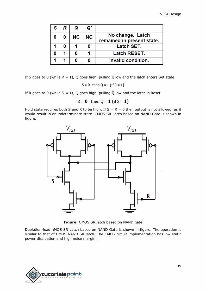
S R Q Q̅ Operation
0 0 Q Q̅ Hold
1 0 1 0 Set
0 1 0 1 Reset
1 1 0 0 Not allowed
CMOS SR latch based on NOR gate is shown in the figure given below.
VLSI Design
38
Figure: CMOS SR latch based on NOR gate
If the S is equal to VOH and the R is equal to VOL, both of the parallel-connected transistors
M1 and M2 will be ON. The voltage on node Q̅ will assume a logic-low level of VOL = 0.
At the same time, both M3 and M4 are turned off, which results in a logic-high voltage VOH
at node Q. If the R is equal to VOH and the S is equal to VOL, M1 and M2 turned off and M3
and M4 turned on.
SR Latch based on NAND Gate
Figure: Gate Level Schematic
Block diagram and gate level schematic of NAND based SR latch is shown in the figure.
The small circles at the S and R input terminals represents that the circuit responds to
active low input signals. The truth table of NAND based SR latch is given in table
VLSI Design
39
If S goes to 0 (while R = 1), Q goes high, pulling Q̅ low and the latch enters Set state
S = 0 then Q = 1 (if R = 1)
If R goes to 0 (while S = 1), Q goes high, pulling Q̅ low and the latch is Reset
R = 0 then Q = 1 (if S = 1)
Hold state requires both S and R to be high. If S = R = 0 then output is not allowed, as it
would result in an indeterminate state. CMOS SR Latch based on NAND Gate is shown in
figure.
Figure: CMOS SR latch based on NAND gate
Depletion-load nMOS SR Latch based on NAND Gate is shown in figure. The operation is
similar to that of CMOS NAND SR latch. The CMOS circuit implementation has low static
power dissipation and high noise margin.
VLSI Design
40
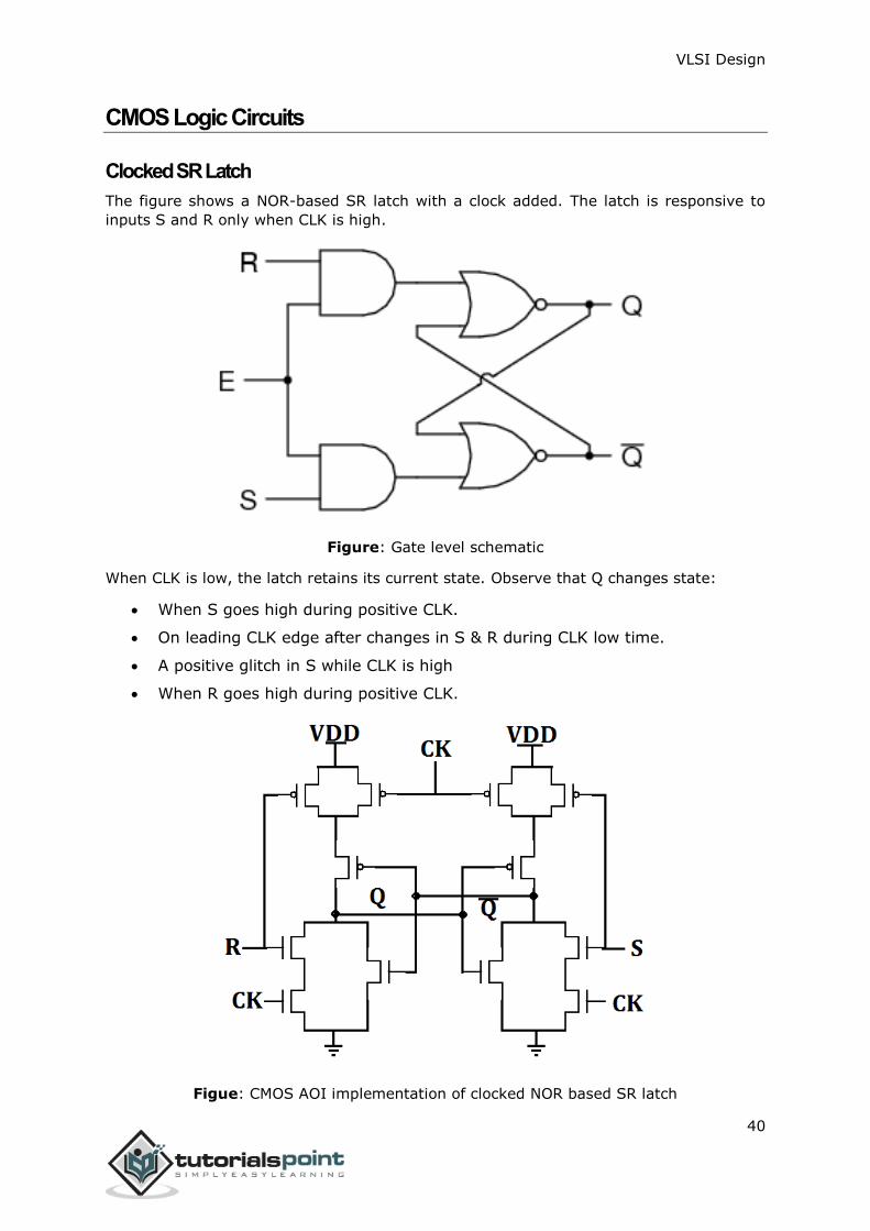
CMOS Logic Circuits
Clocked SR Latch
The figure shows a NOR-based SR latch with a clock added. The latch is responsive to
inputs S and R only when CLK is high.
Figure: Gate level schematic
When CLK is low, the latch retains its current state. Observe that Q changes state:
When S goes high during positive CLK.
On leading CLK edge after changes in S & R during CLK low time.
A positive glitch in S while CLK is high
When R goes high during positive CLK.
Figue: CMOS AOI implementation of clocked NOR based SR latch

VLSI Design
41
CMOS AOI implementation of clocked NOR based SR latch is shown in the figure. Note that
only 12 transistors required.
When CLK is low, two series terminals in N tree N are open and two parallel
transistors in tree P are ON, thus retaining state in the memory cell.
When clock is high, the circuit becomes simply a NOR based CMOS latch which will
respond to input S and R.
Clocked SR Latch based on NAND Gate
Figure: Gate level schematic
Circuit is implemented with four NAND gates. If this circuit is implemented with CMOS
then it requires 16 transistors.
The latch is responsive to S or R only if CLK is high.
If both input signals and the CLK signals are active high: i.e., the latch output Q
will be set when CLK = "1" S = "1" and R = "0"
Similarly, the latch will be reset when CLK = "1," S = "0," and
When CLK is low, the latch retains its present state.
Clocked JK Latch
Figure: Gate level schematic

VLSI Design
42
The figure above shows a clocked JK latch, based on NAND gates. The disadvantage of an
SR latch is that when both S and R are high, its output state becomes indeterminant. The
JK latch eliminates this problem by using feedback from output to input, such that all input
states of the truth table are allowable. If J = K = 0, the latch will hold its present state.
If J = 1 and K = 0, the latch will set on the next positive-going clock edge, i.e. Q = 1, Q ̅
= 0
If J = 0 and K = 1, the latch will reset on the next positive-going clock edge, i.e. Q = 1
and Q ̅ = 0.
If J = K = 1, the latch will toggle on the next positive-going clock edge
The operation of the clocked JK latch is summarized in the truth table given in table.
J K Q Q̅ S R Q Q̅ Operation
0 0 0 1 1 1 0 1
Hold 1 0 1 1 1 0
0 1 0 1 1 1 0 1
Reset 1 0 1 0 0 1
1 0 0 1 0 1 1 0
Set 1 0 1 1 1 0
1 1 0 1 0 1 1 0
toggle 1 0 1 0 0 1
CMOS D Latch Implementation
Figure: Gate level schematic

VLSI Design
43
Figure: CMOS implementation of D Latch
The D latch is normally, implemented with transmission gate (TG) switches as shown in
the figure. The input TG is activated with CLK while the latch feedback loop TG is activated
with CLK. Input D is accepted when CLK is high. When CLK goes low, the input is open-
circuited and the latch is set with the prior data D.

VLSI Design
44
Part 2 – VHDL
VLSI Design
45
VHDL stands for very high-speed integrated circuit hardware description language. It is a
programming language used to model a digital system by dataflow, behavioral and
structural style of modeling. This language was first introduced in 1981 for the department
of Defense (DoD) under the VHSIC program.
Describing a Design
In VHDL an entity is used to describe a hardware module. An entity can be described
using,
1. Entity declaration
2. Architecture
3. Configuration
4. Package declaration
5. Package body
Let’s see what are these?
Entity Declaration
It defines the names, input output signals and modes of a hardware module.
Syntax:
entity entity_name is
Port declaration;
end entity_name;
An entity declaration should start with ‘entity’ and end with ‘end’ keywords. The direction
will be input, output or inout.
In Port can be read
Out Port can be written
Inout Port can be read and written
Buffer Port can be read and written, it
can have only one source.
Architecture:
Architecture can be described using structural, dataflow, behavioral or mixed style.
7. VHDL – Introduction

VLSI Design
46
Syntax:
architecture architecture_name of entity_name
architecture_declarative_part;
begin
Statements;
end architecture_name;
Here, we should specify the entity name for which we are writing the architecture body.
The architecture statements should be inside the ‘begin’ and ‘énd’ keyword. Architecture
declarative part may contain variables, constants, or component declaration.
Data Flow Modeling
In this modeling style, the flow of data through the entity is expressed using concurrent
(parallel) signal. The concurrent statements in VHDL are WHEN and GENERATE.
Besides them, assignments using only operators (AND, NOT, +, *, sll, etc.) can also be
used to construct code.
Finally, a special kind of assignment, called BLOCK, can also be employed in this kind of
code.
In concurrent code, the following can be used:
Operators
The WHEN statement (WHEN/ELSE or WITH/SELECT/WHEN);
The GENERATE statement;
The BLOCK statement
Behavioral Modeling
In this modeling style, the behavior of an entity as set of statements is executed
sequentially in the specified order. Only statements placed inside a PROCESS, FUNCTION,
or PROCEDURE are sequential.
PROCESSES, FUNCTIONS, and PROCEDURES are the only sections of code that are
executed sequentially.
However, as a whole, any of these blocks is still concurrent with any other statements
placed outside it.
One important aspect of behavior code is that it is not limited to sequential logic. Indeed,
with it, we can build sequential circuits as well as combinational circuits.
The behavior statements are IF, WAIT, CASE, and LOOP. VARIABLES are also restricted
and they are supposed to be used in sequential code only. VARIABLE can never be global,
so its value cannot be passed out directly.
Structural Modeling
In this modeling, an entity is described as a set of interconnected components. A
component instantiation statement is a concurrent statement. Therefore, the order of
these statements is not important. The structural style of modeling describes only an
VLSI Design
47
interconnection of components (viewed as black boxes), without implying any behavior of
the components themselves nor of the entity that they collectively represent.
In Structural modeling, architecture body is composed of two parts: the declarative part
(before the keyword begin) and the statement part (after the keyword begin).
Logic Operation – AND GATE
Symbol: Truth Table:
VHDL Code:
Library ieee;
use ieee.std_logic_1164.all;
entity and1 is
port(x,y:in bit ; z:out bit);
end and1;
architecture virat of and1 is begin
z<=x and y;
end virat;
Waveforms:
X Y Z 0 0 0 0 1 0 1 0 0 1 1 1

VLSI Design
48
Logic Operation – OR Gate
Symbol: Truth Table:
VHDL Code:
Library ieee;
use ieee.std_logic_1164.all;
entity or1 is
port(x,y:in bit ; z:out bit);
end or1;
architecture virat of or1 is begin
z<=x or y;
end virat;
Waveforms:
Logic Operation – NOT Gate
Symbol: Truth Table:
X Y Z 0 0 0 0 1 1 1 0 1 1 1 1
X Y 0 1 1 0
VLSI Design
49
VHDL Code:
Library ieee;
use ieee.std_logic_1164.all;
entity not1 is
port(x:in bit ; y:out bit);
end not1;
architecture virat of not1 is begin
y<=not x;
end virat;
Waveforms:
Logic Operation – NAND Gate
Symbol: Truth Table:
VHDL Code:
Library ieee;
use ieee.std_logic_1164.all;
X Y Z 0 0 1 0 1 1 1 0 1 1 1 0
VLSI Design
50
entity nand1 is
port(a,b:in bit ; c:out bit);
end nand1;
architecture virat of nand1 is begin
c<=a nand b;
end virat;
Waveforms:
Logic Operation – NOR Gate
Symbol: Truth Table:
VHDL Code:
Library ieee;
use ieee.std_logic_1164.all;
entity nor1 is
port(a,b:in bit ; c:out bit);
end nor1;
architecture virat of nor1 is begin
X Y Z 0 0 1 0 1 0 1 0 0 1 1 0
VLSI Design
51
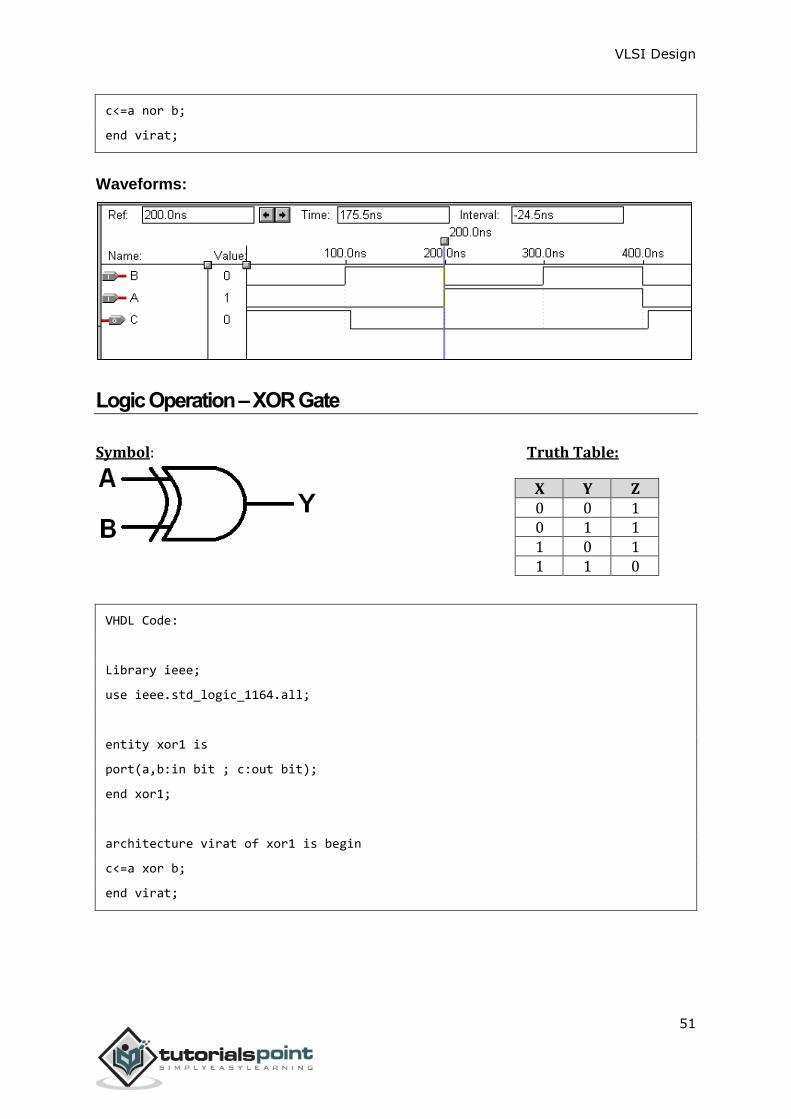
c<=a nor b;
end virat;
Waveforms:
Logic Operation – XOR Gate
Symbol: Truth Table:
VHDL Code:
Library ieee;
use ieee.std_logic_1164.all;
entity xor1 is
port(a,b:in bit ; c:out bit);
end xor1;
architecture virat of xor1 is begin
c<=a xor b;
end virat;
X Y Z 0 0 1 0 1 1 1 0 1 1 1 0

VLSI Design
52
Waveforms:
Logic Operation – X-NOR Gate
Symbol: Truth Table:
VHDL Code:
Library ieee;
use ieee.std_logic_1164.all;
entity xnor1 is
port(a,b:in bit ; c:out bit);
end xnor1;
architecture virat of xnor1 is begin
c<=not(a xor b);
end virat;
X Y Z 0 0 1 0 1 1 1 0 1 1 1 0
VLSI Design
53
Waveforms
VLSI Design
54
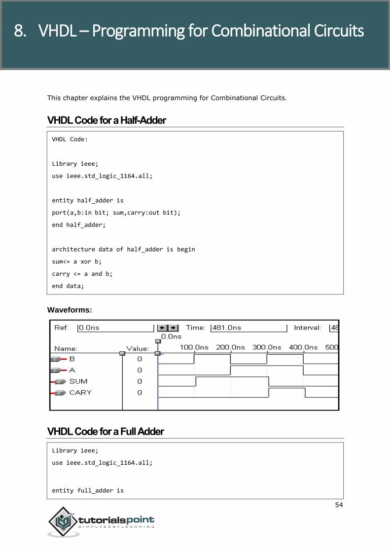
This chapter explains the VHDL programming for Combinational Circuits.
VHDL Code for a Half-Adder
VHDL Code:
Library ieee;
use ieee.std_logic_1164.all;
entity half_adder is
port(a,b:in bit; sum,carry:out bit);
end half_adder;
architecture data of half_adder is begin
sum<= a xor b;
carry <= a and b;
end data;
Waveforms:
VHDL Code for a Full Adder
Library ieee;
use ieee.std_logic_1164.all;
entity full_adder is
8. VHDL – Programming for Combinational Circuits

VLSI Design
55
port(a,b,c:in bit; sum,carry:out bit);
end full_adder;
architecture data of full_adder is begin
sum<= a xor b xor c;
carry <= ((a and b) or (b and c) or (a and c));
end data;
Waveforms:
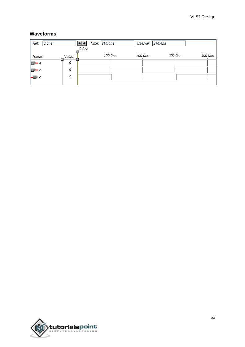
VHDL Code for a Half-Subtractor
Library ieee;
use ieee.std_logic_1164.all;
entity half_sub is
port(a,c:in bit; d,b:out bit);
end half_sub;
architecture data of half_sub is begin
d<= a xor c;
b<= (a and (not c));
end data;
Waveforms:
VLSI Design
56
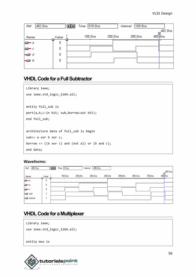
VHDL Code for a Full Subtractor
Library ieee;
use ieee.std_logic_1164.all;
entity full_sub is
port(a,b,c:in bit; sub,borrow:out bit);
end full_sub;
architecture data of full_sub is begin
sub<= a xor b xor c;
borrow <= ((b xor c) and (not a)) or (b and c);
end data;
Waveforms:
VHDL Code for a Multiplexer
Library ieee;
use ieee.std_logic_1164.all;
entity mux is
VLSI Design
57
port(S1,S0,D0,D1,D2,D3:in bit; Y:out bit);
end mux;
architecture data of mux is begin
Y<= (not S0 and not S1 and D0) or (S0 and not S1 and D1) or (not S0 and S1 and
D2) or (S0 and S1 and D3);
end data;
Waveforms:
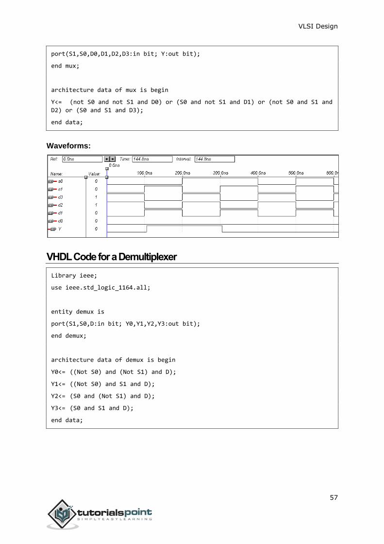
VHDL Code for a Demultiplexer
Library ieee;
use ieee.std_logic_1164.all;
entity demux is
port(S1,S0,D:in bit; Y0,Y1,Y2,Y3:out bit);
end demux;
architecture data of demux is begin
Y0<= ((Not S0) and (Not S1) and D);
Y1<= ((Not S0) and S1 and D);
Y2<= (S0 and (Not S1) and D);
Y3<= (S0 and S1 and D);
end data;

VLSI Design
58
Waveforms:
VHDL Code for a 8 x 3 Encoder:
library ieee;
use ieee.std_logic_1164.all;
entity enc is
port(i0,i1,i2,i3,i4,i5,i6,i7:in bit; o0,o1,o2: out bit);
end enc;
architecture vcgandhi of enc is
begin
o0<=i4 or i5 or i6 or i7;
o1<=i2 or i3 or i6 or i7;
o2<=i1 or i3 or i5 or i7;
end vcgandhi;
Waveforms:
VHDL Code for a 3 x 8 Decoder
library ieee;
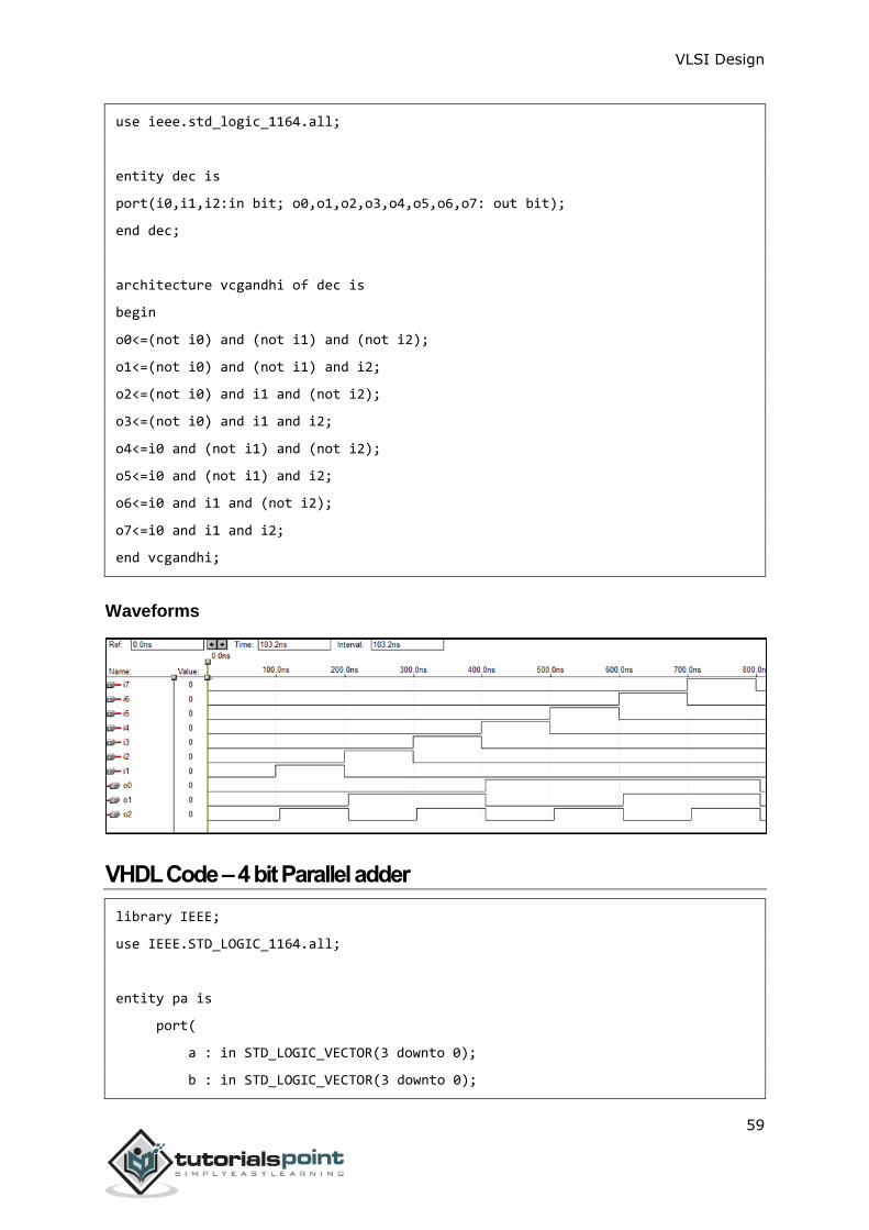
VLSI Design
59
use ieee.std_logic_1164.all;
entity dec is
port(i0,i1,i2:in bit; o0,o1,o2,o3,o4,o5,o6,o7: out bit);
end dec;
architecture vcgandhi of dec is
begin
o0<=(not i0) and (not i1) and (not i2);
o1<=(not i0) and (not i1) and i2;
o2<=(not i0) and i1 and (not i2);
o3<=(not i0) and i1 and i2;
o4<=i0 and (not i1) and (not i2);
o5<=i0 and (not i1) and i2;
o6<=i0 and i1 and (not i2);
o7<=i0 and i1 and i2;
end vcgandhi;
Waveforms
VHDL Code – 4 bit Parallel adder
library IEEE;
use IEEE.STD_LOGIC_1164.all;
entity pa is
port(
a : in STD_LOGIC_VECTOR(3 downto 0);
b : in STD_LOGIC_VECTOR(3 downto 0);
VLSI Design
60
ca : out STD_LOGIC;
sum : out STD_LOGIC_VECTOR(3 downto 0)
);
end pa;
architecture vcgandhi of pa is
Component fa is
port (a : in STD_LOGIC;
b : in STD_LOGIC;
c : in STD_LOGIC;
sum : out STD_LOGIC;
ca : out STD_LOGIC
);
end component;
signal s : std_logic_vector (2 downto 0);
signal temp: std_logic;
begin
temp<='0';
u0 : fa port map (a(0),b(0),temp,sum(0),s(0));
u1 : fa port map (a(1),b(1),s(0),sum(1),s(1));
u2 : fa port map (a(2),b(2),s(1),sum(2),s(2));
ue : fa port map (a(3),b(3),s(2),sum(3),ca);
end vcgandhi;
Waveforms:
VLSI Design
61
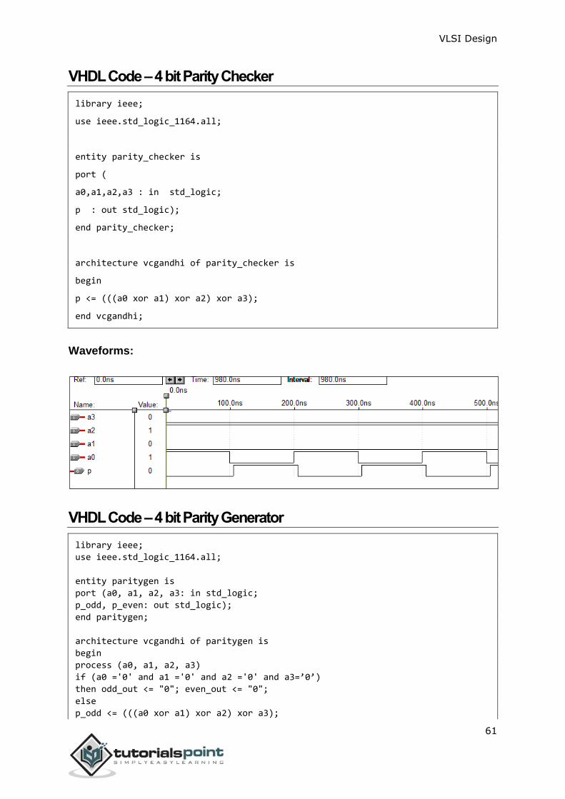
VHDL Code – 4 bit Parity Checker
library ieee;
use ieee.std_logic_1164.all;
entity parity_checker is
port (
a0,a1,a2,a3 : in std_logic;
p : out std_logic);
end parity_checker;
architecture vcgandhi of parity_checker is
begin
p <= (((a0 xor a1) xor a2) xor a3);
end vcgandhi;
Waveforms:
VHDL Code – 4 bit Parity Generator
library ieee;
use ieee.std_logic_1164.all;
entity paritygen is
port (a0, a1, a2, a3: in std_logic;
p_odd, p_even: out std_logic);
end paritygen;
architecture vcgandhi of paritygen is
begin
process (a0, a1, a2, a3)
if (a0 ='0' and a1 ='0' and a2 ='0' and a3=’0’)
then odd_out <= "0"; even_out <= "0";
else
p_odd <= (((a0 xor a1) xor a2) xor a3);

VLSI Design
62
p_even <= not(((a0 xor a1) xor a2) xor a3);
end vcgandhi;
Waveforms:

VLSI Design
63
This chapter explains how to do VHDL programming for Sequential Circuits.
VHDL Code for an SR Latch
library ieee;
use ieee.std_logic_1164.all;
entity srl is
port(r,s:in bit; q,qbar:buffer bit);
end srl;
architecture virat of srl is
signal s1,r1:bit;
begin
q<= s nand qbar;
qbar<= r nand q;
end virat;
Waveforms:
VHDL Code for a D Latch
library ieee;
use ieee.std_logic_1164.all;
9. VHDL – Programming for Sequential Crcuits
VLSI Design
64
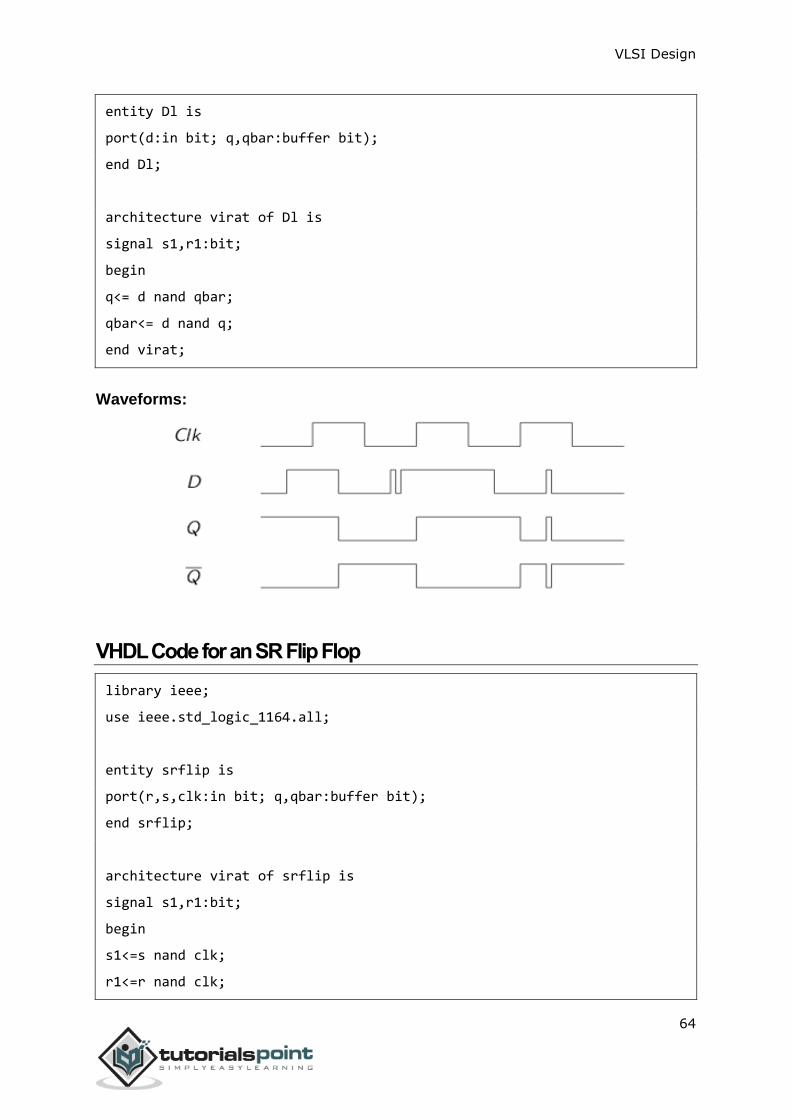
entity Dl is
port(d:in bit; q,qbar:buffer bit);
end Dl;
architecture virat of Dl is
signal s1,r1:bit;
begin
q<= d nand qbar;
qbar<= d nand q;
end virat;
Waveforms:
VHDL Code for an SR Flip Flop
library ieee;
use ieee.std_logic_1164.all;
entity srflip is
port(r,s,clk:in bit; q,qbar:buffer bit);
end srflip;
architecture virat of srflip is
signal s1,r1:bit;
begin
s1<=s nand clk;
r1<=r nand clk;

VLSI Design
65
q<= s1 nand qbar;
qbar<= r1 nand q;
end virat;
Waveforms
VHDL code for a JK Flip Flop
library IEEE;
use IEEE.STD_LOGIC_1164.all;
entity jk is
port(
j : in STD_LOGIC;
k : in STD_LOGIC;
clk : in STD_LOGIC;
reset : in STD_LOGIC;
q : out STD_LOGIC;
qb : out STD_LOGIC
);
end jk;
architecture virat of jk is
begin
jkff : process (j,k,clk,reset) is
variable m : std_logic := '0';
begin
if (reset='1') then
m := '0';
elsif (rising_edge (clk)) then
if (j/=k) then
m := j;

VLSI Design
66
elsif (j='1' and k='1') then
m := not m;
end if;
end if;
q <= m;
qb <= not m;
end process jkff;
end virat;
Waveforms:
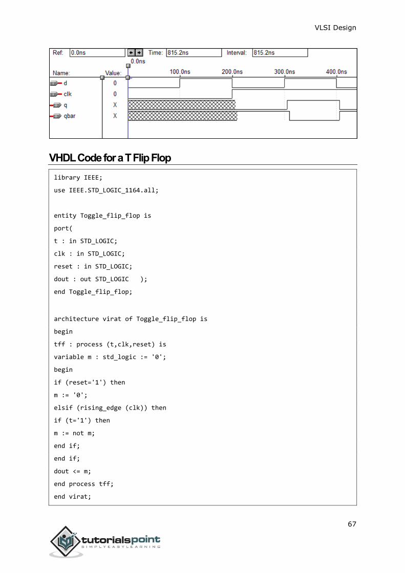
VHDL Code for a D Flip Flop
Library ieee;
use ieee.std_logic_1164.all;
entity dflip is
port(d,clk:in bit; q,qbar:buffer bit);
end dflip;
architecture virat of dflip is
signal d1,d2:bit;
begin
d1<=d nand clk;
d2<=(not d) nand clk;
q<= d1 nand qbar;
qbar<= d2 nand q;
end virat;
Waveforms:
VLSI Design
67
VHDL Code for a T Flip Flop
library IEEE;
use IEEE.STD_LOGIC_1164.all;
entity Toggle_flip_flop is
port(
t : in STD_LOGIC;
clk : in STD_LOGIC;
reset : in STD_LOGIC;
dout : out STD_LOGIC );
end Toggle_flip_flop;
architecture virat of Toggle_flip_flop is
begin
tff : process (t,clk,reset) is
variable m : std_logic := '0';
begin
if (reset='1') then
m := '0';
elsif (rising_edge (clk)) then
if (t='1') then
m := not m;
end if;
end if;
dout <= m;
end process tff;
end virat;
VLSI Design
68
Waveforms:
VHDL Code for a 4 - bit Up Counter
library IEEE;
use ieee.std_logic_1164.all;
use ieee.std_logic_unsigned.all;
entity counter is
port(Clock, CLR : in std_logic;
Q : out std_logic_vector(3 downto 0));
end counter;
architecture virat of counter is
signal tmp: std_logic_vector(3 downto 0);
begin
process (Clock, CLR)
begin
if (CLR='1') then
tmp <= "0000";
elsif (Clock'event and Clock='1') then
tmp <= tmp + 1;
end if;
end process;
Q <= tmp;
end virat;
Waveforms:

VLSI Design
69
VHDL Code for a 4-bit Down Counter
library ieee;
use ieee.std_logic_1164.all;
use ieee.std_logic_unsigned.all;
entity dcounter is
port(Clock, CLR : in std_logic;
Q : out std_logic_vector(3 downto 0));
end dcounter;
architecture virat of dcounter is
signal tmp: std_logic_vector(3 downto 0);
begin
process (Clock, CLR)
begin
if (CLR='1') then
tmp <= "1111";
elsif (Clock'event and Clock='1') then
tmp <= tmp - 1;
end if;
end process;
Q <= tmp;
end virat;

VLSI Design
70
Waveforms:
VLSI Design
71
Part 3 – Verilog
VLSI Design
72
Verilog is a HARDWARE DESCRIPTION LANGUAGE (HDL). It is a language used for
describing a digital system like a network switch or a microprocessor or a memory or a
flip−flop. It means, by using a HDL we can describe any digital hardware at any level.
Designs, which are described in HDL are independent of technology, very easy for
designing and debugging, and are normally more useful than schematics, particularly for
large circuits.
Verilog supports a design at many levels of abstraction. The major three are:
Behavioral level
Register-transfer level
Gate level
Behavioral level
This level describes a system by concurrent algorithms (Behavioural). Every algorithm is
sequential, which means it consists of a set of instructions that are executed one by one.
Functions, tasks and blocks are the main elements. There is no regard to the structural
realization of the design.
Register−Transfer Level
Designs using the Register−Transfer Level specify the characteristics of a circuit using
operations and the transfer of data between the registers. Modern definition of an RTL
code is "Any code that is synthesizable is called RTL code".
Gate Level
Within the logical level, the characteristics of a system are described by logical links and
their timing properties. All signals are discrete signals. They can only have definite logical
values (`0', `1', `X', `Z`). The usable operations are predefined logic primitives (basic
gates). Gate level modelling may not be a right idea for logic design. Gate level code is
generated using tools like synthesis tools and his netlist is used for gate level simulation and for backend.
Lexical Tokens
Verilog language source text files are a stream of lexical tokens. A token consists of one
or more characters, and each single character is in exactly one token.
The basic lexical tokens used by the Verilog HDL are similar to those in C Programming
Language. Verilog is case sensitive. All the key words are in lower case.
10. Verilog – Introduction
VLSI Design
73
White Space
White spaces can contain characters for spaces, tabs, new-lines and form feeds. These
characters are ignored except when they serve to separate tokens.
White space characters are Blank space, Tabs, Carriage returns, New line, and Form feeds.
Comments
There are two forms to represent the comments
1) Single line comments begin with the token // and end with carriage return.
Ex.: //this is single line syntax
2) Multiline comments begins with the token /* and end with token */
Ex.: /* this is multiline Syntax*/
Numbers
You can specify a number in binary, octal, decimal or hexadecimal format. Negative
numbers are represented in 2’s compliment numbers. Verilog allows integers, real
numbers and signed & unsigned numbers.
The syntax is given by: <size> <radix> <value>
Size or unsized number can be defined in <Size> and <radix> defines whether it is binary,
octal, hexadecimal or decimal.
Identifiers
Identifier is the name used to define the object, such as a function, module or register.
Identifiers should begin with an alphabetical characters or underscore characters. Ex. A_Z,
a_z,_
Identifiers are a combination of alphabetic, numeric, underscore and $ characters. They
can be up to 1024 characters long.
Operators
Operators are special characters used to put conditions or to operate the variables. There
are one, two and sometimes three characters used to perform operations on variables.
Ex. >, +, ~, &! =.
Verilog Keywords
Words that have special meaning in Verilog are called the Verilog keywords. For example,
assign, case, while, wire, reg, and, or, nand, and module. They should not be used as
identifiers. Verilog keywords also include compiler directives, and system tasks and
functions.
Gate Level Modelling
Verilog has built-in primitives like logic gates, transmission gates and switches. These are
rarely used for design work but they are used in post synthesis world for modelling of
ASIC/FPGA cells.
VLSI Design
74
Gate level modelling exhibits two properties:
Drive strength: The strength of the output gates is defined by drive strength. The output
is strongest if there is a direct connection to the source. The strength decreases if the
connection is via a conducting transistor and least when connected via a pull-up/down
resistive. The drive strength is usually not specified, in which case the strengths defaults
to strong1 and strong0.
Delays: If delays are not specified, then the gates do not have propagation delays; if two
delays are specified, then first one represents the rise delay and the second one, fall delay;
if only one delay is specified, then both, rise and fall are equal. Delays can be ignored in
synthesis.
Gate Primitives
The basic logic gates using one output and many inputs are used in Verilog. GATE uses
one of the keywords - and, nand, or, nor, xor, xnor for use in Verilog for N number of
inputs and 1 output.
Example:
Module gate()
Wire ot0;
Wire ot1;
Wire ot2;
Reg in0,in1,in2,in3;
Not U1(ot0,in0);
Xor U2(ot1,in1,in2,in3);
And U3(ot2, in2,in3,in0)
Transmission Gate Primitives
Transmission gate primitives include both, buffers and inverters. They have single input
and one or more outputs. In the gate instantiation syntax shown below, GATE stands for
either the keyword buf or NOT gate.
Example: Not, buf, bufif0, bufif1, notif0, notif1
Not – n outout inverter
Buf – n output buffer
Bufifo – tristate buffer, active low enable
Bufif1 – tristate buffer, active high enable
Notifo – tristate inverter, active low enable
Notif1 – tristate inverter, active high enable
Example:
Module gate()
Wire out0;
Wire out1;
Reg in0,in1;

VLSI Design
75
Not U1(out0,in0);
Buf U2(out0,in0);
Data Types
Value Set
Verilog consists of, mainly, four basic values. All Verilog data types, which are used in
Verilog store these values:
0 (logic zero, or false condition)
1 (logic one, or true condition)
x (unknown logic value)
z (high impedance state)
use of x and z is very limited for synthesis.
Wire
A wire is used to represent a physical wire in a circuit and it is used for connection of gates
or modules. The value of a wire can only be read and not assigned in a function or block.
A wire cannot store value but is always driven by a continuous assignment statement or
by connecting wire to output of a gate/module. Other specific types of wires are:
Wand (wired-AND): here value of Wand is dependent on logical AND of all the device
drivers connected to it.
Wor (wired-OR): here value of a Wor is dependent on logical OR of all the device drivers
connected to it.
Tri (three-state): here all drivers connected to a tri must be z, except only one (which
determines value of tri).
Example:
Wire [msb:lsb] wire_variable_list;
Wirec // simple wire
Wand d;
Assign d = a; // value of d is the logical AND of
Assign d = b; // a and b
Wire [9:0] A; // a cable (vector) of 10 wires.
Wand [msb:lsb] wand_variable_list;
Wor [msb:lsb] wor_variable_list;
Tri [msb:lsb] tri_variable_list;

VLSI Design
76
Register
A reg (register) is a data object, which is holding the value from one procedural assignment
to next one and are used only in different functions and procedural blocks. A reg is a simple
Verilog, variable-type register and can’t imply a physical register. In multi-bit registers,
the data is stored in the form of unsigned numbers and sign extension is not used.
Example:
reg c; // single 1-bit register variable
reg [5:0] gem; // a 6-bit vector;
reg [6:0] d, e; // two 7-bit variables
Input, Output, Inout
These keywords are used to declare input, output and bidirectional ports of a task or
module. Here input and inout ports, which are of wire type and output port is configured
to be of wire, reg, wand, wor or tri type. Always, default is wire type.
Example
Module sample(a, c, b, d);
Input c; // An input where wire is used.
Output a, b; // Two outputs where wire is used.
Output [2:0] d; /* A three-bit output. One must declare type in a separate
statement. */
reg [1:0] a; // The above ‘a’ port is for declaration in reg.
Integer
Integers are used in general-purpose variables. They are used mainly in loops-indicies,
constants, and parameters. They are of ‘reg’ type data type. They store data as signed
numbers whereas explicitly declared reg types store them as an unsigned data. If the
integer is not defined at the time of compiling, then the default size would be 32 bits.
If an integer holds a constant, the synthesizer adjusts them to the minimum width needed
at the time of compilation.
Example
Integer c; // single 32-bit integer
Assign a=63; // 63 defaults to a 7-bit variable.
Supply0, Supply1
Supply0 define wires tied to logic 0 (ground) and supply1 define wires tied to logic 1
(power).
Example
supply0 logic_0_wires;
supply0 gnd1; // equivalent to a wire assigned as 0
VLSI Design
77
supply1 logic_1_wires;
supply1 c, s;
Time
Time is a 64-bit quantity that can be used in conjunction with the $time system task to
hold simulation time. Time is not supported for synthesis and hence is used only for
simulation purposes.
Example
time time_variable_list;
time c;
c = $time; //c = current simulation time
Parameter
A parameter is defining a constant which can be set when you use a module, which allows
customization of module during the instantiation process.
Example
Parameter add = 3’b010, sub = 2’b11;
Parameter n = 3;
Parameter [2:0] param2 = 3’b110;
reg [n-1:0] jam; /* A 3-bit register with length of n or above. */
always @(z)
y = {{(add - sub){z}};
if (z) begin
state = param2[1]; else state = param2[2];
end
Operators
Arithmetic Operators
These operators is perform arithmetic operations. The + and - are used as either unary (-
x) or binary (z-y) operators.
The Operators which are included in arithmetic operation are:
+ (addition), - (subtraction), * (multiplication), / (division), % (modulus)
Example:
parameter v = 5;

VLSI Design
78
reg[3:0] b, d, h, i, count;
h = b + d;
i = d - v;
cnt = (cnt +1)%16; //Can count 0 thru 15.
Relational Operators
These operators compare two operands and return the result in a single bit, 1 or 0.
Wire and reg variables are positive. Thus (-3’d001) = = 3’d111 and (-3b001)>3b110.
The Operators which are included in relational operation are:
== (equal to)
!= (not equal to)
> (greater than)
>= (greater than or equal to)
< (less than)
<= (less than or equal to)
Example
if (z = = y) c = 1;
else c = 0; // Compare in 2’s compliment; d>b
reg [3:0] d,b;
if (d[3]= = b[3]) d[2:0] > b[2:0];
else b[3];
Equivalent Statement
e = (z == y);
Bit-wise Operators
Bit-wise operators which are doing a bit-by-bit comparison between two operands.
The Operators which are included in Bit wise operation are:
& (bitwise AND)
| (bitwiseOR)
~ (bitwise NOT)
^ (bitwise XOR)
~^ or ^~(bitwise XNOR)
VLSI Design
79
Example
module and2 (d, b, c);
input [1:0] d, b;
output [1:0] c;
assign c = d & b;
end module
Logical Operators
Logical operators are bit-wise operators and are used only for single-bit operands. They
return a single bit value, 0 or 1. They can work on integers or group of bits, expressions
and treat all non-zero values as 1. Logical operators are generally, used in conditional
statements since they work with expressions.
The operators which are included in Logical operation are:
! (logical NOT)
&& (logical AND)
|| (logical OR)
Example
wire[7:0] a, b, c; // a, b and c are multibit variables.
reg x;
if ((a == b) && (c)) x = 1; //x = 1 if x equals b, and c is nonzero.
else x = !a; // x =0 if a is anything but zero.
Reduction Operators
Reduction operators are the unary form of the bitwise operators and operate on all the
bits of an operand vector. These also return a single-bit value.
The operators which are included in Reduction operation are:
& (reduction AND)
| (reduction OR)
~& (reduction NAND)
~| (reduction NOR)
^ (reduction XOR)
~^ or ^~(reduction XNOR)
Example

VLSI Design
80
Module chk_zero (x, z);
Input [2:0] x;
Output z;
Assign z = & x; // Reduction AND
End module
Shift Operators
Shift operators, which are shifting the first operand by the number of bits specified by
second operand in the syntax. Vacant positions are filled with zeros for both directions,
left and right shifts (There is no use sign extension).
The Operators which are included in Shift operation are:
<< (shift left)
>> (shift right)
Example:
Assign z = c << 3; /* z = c shifted left 3 bits;
Vacant positions are filled with 0’s */
Concatenation Operator
The concatenation operator combines two or more operands to form a larger vector.
The operator included in Concatenation operation is: { }(concatenation)
Example
wire [1:0] a, h; wire [2:0] x; wire [3;0] y, Z;
assign x = {1’b0, a}; // x[2]=0, x[1]=a[1], x[0]=a[0]
assign b = {a, h}; /* b[3]=a[1], b[2]=a[0], b[1]=h[1],
b[0]=h[0] */
assign {cout, b} = x + Z; // Concatenation of a result
Replication Operator
The replication operator are making multiple copies of an item.
The operator used in Replication operation is: {n{item}} (n fold replication of an item)
Example
Wire [1:0] a, f; wire [4:0] x;
Assign x = {2{1’f0}, a}; // Equivalent to x = {0,0,a }
Assign y = {2{a}, 3{f}}; //Equivalent to y = {a,a,f,f}

VLSI Design
81
For synthesis, Synopsis did not like a zero replication.
For example:-
Parameter l=5, k=5;
Assign x= {(l-k){a}}
Conditional Operator
Conditional operator synthesizes to a multiplexer. It is the same kind as is used in C/C++
and evaluates one of the two expressions based on the condition.
The operator used in Conditional operation is:
(Condition) ? (Result if condition true):
(result if condition false)
Example
Assign x = (g) ? a : b;
Assign x = (inc = = 2) ? x+1 : x-1;
/* if (inc), x = x+1, else x = x-1 */
Operands
Literals
Literals are constant-valued operands that are used in Verilog expressions. The two
commonly used Verilog literals are:
String: A string literal operand is a one-dimensional array of characters, which are
enclosed in double quotes (" ").
Numeric: A constant number operand is specified in binary, octal, decimal or
hexadecimal Number.
Example
n - integer representing number of bits
F - one of four possible base formats:
b for binary, o for octal, d for decimal, h for hexadecimal.
“time is” // string literal
267 // 32-bit decimal number
2’b01 // 2-bit binary
20’hB36F // 20-bit hexadecimal number
‘062 // 32-bit octal number
VLSI Design
82
Wires, Regs, and Parameters
Wires, regs and parameters are the data types used as operands in Verilog expressions.
Bit-Selection “x[2]” and Part-Selection “x[4:2]”
Bit-selects and part-selects are used to select one bit and a multiple bits, respectively,
from a wire, reg or parameter vector with the use of square brackets “[ ]”. Bit-selects and
part-selects are also used as operands in expressions in the same way that their main
data objects are used.
Example
reg [7:0] x, y;
reg [3:0] z;
reg a;
a = x[7] & y[7]; // bit-selects
z = x[7:4] + y[3:0]; // part-selects
Function Calls
In the Function calls, the return value of a function is used directly in an expression without
the need of first assigning it to a register or wire. It just place the function call as one of
the type of operands.it is needful to make sure you are knowing the bit width of the return
value of function call.
Example
Assign x = y & z & chk_yz(z, y);// chk_yz is a function
. . ./* Definition of the function */
Function chk_yz;// function definition
Input z,y;
chk_yz = y^z;
End function
Modules
Module Declaration
In Verilog, A module is the principal design entity. This indicates the name and port list
(arguments). The next few lines which specifies the input/output type (input, output or
inout) and width of the each port. The default port width is only 1 bit. The port variables
must be declared by wire, wand,. . ., reg. The default port variable is wire. Normally,
inputs are wire because their data is latched outside the module. Outputs are of reg type
if their signals are stored inside.
Example
VLSI Design
83
module sub_add(add, in1, in2, out);
input add; // defaults to wire
input [7:0] in1, in2; wire in1, in2;
output [7:0] out; reg out;
... statements ...
End module
Continuous Assignment
The continuous assignment in a Module is used for assigning a value on to a wire, which
is the normal assignment used at outside of always or initial blocks. This assignment is
done with an explicit assign statement or to assign a value to a wire during its declaration.
Continuous assignment are continuously executed at the time of simulation. The order of
assign statements does not affect it. If you do any change in any of the right-hand-side
inputs signal it will change a left-hand-side output signal.
Example
Wire [1:0] x = 2’y01; // assigned on declaration
Assign y = c | d; // using assign statement
Assign d = a & b;
/* the order of the assign statements does not matter. */
Module Instantiations
Module declarations are templates for creating actual objects. Modules are instantiated
inside other modules, and each instantiation is creating a single object from that template.
The exception is the top-level module which is its own instantiation. The module’s ports
must to be matched to those which are defined in the template. It is specified:
By name, using a dot “.template port name (name of wire connected to port)”. Or
By position, placing the ports in the same place in the port lists of both of the
template and the instance.
Example
MODULE DEFINITION
Module and4 (x, y, z);
Input [3:0] x, y;
Output [3:0] z;
Assign z = x | y;
End module

VLSI Design
84
Behavioral models in Verilog contain procedural statements, which control the simulation
and manipulate variables of the data types. These all statements are contained within the
procedures. Each of the procedure has an activity flow associated with it.
During simulation of behavioral model, all the flows defined by the ‘always’ and ‘initial’
statements start together at simulation time ‘zero’. The initial statements are executed
once, and the always statements are executed repetitively. In this model, the register
variables a and b are initialized to binary 1 and 0 respectively at simulation time ‘zero’.
The initial statement is then completed and is not executed again during that simulation
run. This initial statement is containing a begin-end block (also called a sequential block)
of statements. In this begin-end type block, a is initialized first followed by b.
Example of Behavioral Modeling
module behave;
reg [1:0]a,b;
initial
begin
a = ’b1;
b = ’b0;
end
always
begin
#50 a = ~a;
end
always
begin
#100 b = ~b;
end
End module
Procedural Assignments
Procedural assignments are for updating reg, integer, time, and memory variables. There
is a significant difference between procedural assignment and continuous assignment as
described below:
Continuous assignments drive net variables and are evaluated and updated whenever an
input operand changes value.
11. Verilog – Behavioral Modelling & Timing Control

VLSI Design
85
Procedural assignments update the value of register variables under the control of the
procedural flow constructs that surround them.
The right-hand side of a procedural assignment can be any expression that evaluates to a
value. However, part-selects on the right-hand side must have constant indices. The left-
hand side indicates the variable that receives the assignment from the right-hand side.
The left-hand side of a procedural assignment can take one of the following forms:
register, integer, real, or time variable: An assignment to the name reference of
one of these data types.
bit-select of a register, integer, real, or time variable: An assignment to a single
bit that leaves the other bits untouched.
part-select of a register, integer, real, or time variable: A part-select of two or more
contiguous bits that leaves the rest of the bits untouched. For the part-select form,
only constant expressions are legal.
memory element: A single word of a memory. Note that bit-selects and part-selects
are illegal on memory element references.
concatenation of any of the above: A concatenation of any of the previous four
forms can be specified, which effectively partitions the result of the right-hand side
expression and assigns the partition parts, in order, to the various parts of the
concatenation.
Delay in Assignment (not for synthesis)
In a delayed assignment Δt time units pass before the statement is executed and the left-
hand assignment is made. With intra-assignment delay, the right side is evaluated
immediately but there is a delay of Δt before the result is place in the left hand assignment.
If another procedure changes a right-hand side signal during Δt, it does not effect the
output. Delays are not supported by synthesis tools.
Syntax
Procedural Assignment variable = expression
Delayed assignment #Δt variable = expression;
Intra-assignment delay variable = #Δt expression;
Example
reg [6:0] sum; reg h, ziltch;
sum[7] = b[7] ^ c[7]; // execute now.
ziltch = #15 ckz&h; /* ckz&a evaluated now; ziltch changed
after 15 time units. */
#10 hat = b&c; /* 10 units after ziltch changes, b&c is
VLSI Design
86
evaluated and hat changes. */
Blocking Assignments
A blocking procedural assignment statement must be executed before the execution of the
statements that follow it in a sequential block. A blocking procedural assignment statement
does not prevent the execution of statements that follow it in a parallel block.
Syntax:
The syntax for a blocking procedural assignment is as follows:
<lvalue> = <timing_control> <expression>
Where, lvalue is a data type that is valid for a procedural assignment statement, = is the
assignment operator, and timing control is the optional intra- assignment delay. The timing
control delay can be either a delay control (for example, #6) or an event control (for
example, @(posedge clk)). The expression is the right-hand side value the simulator
assigns to the left-hand side. The = assignment operator used by blocking procedural
assignments is also used by procedural continuous assignments and continuous
assignments.
Example
rega = 0;
rega[3] = 1; // a bit-select
rega[3:5] = 7; // a part-select
mema[address] = 8’hff; // assignment to a memory element
{carry, acc} = rega + regb; // a concatenation
Nonblocking (RTL) Assignments
The non-blocking procedural assignment allows you to schedule assignments without
blocking the procedural flow. You can use the non-blocking procedural statement
whenever you want to make several register assignments within the same time step
without regard to order or dependance upon each other.
Syntax
The syntax for a non-blocking procedural assignment is as follows:
<lvalue> <= <timing_control> <expression>
Where lvalue is a data type that is valid for a procedural assignment statement,
<= is the non-blocking assignment operator, and timing control is the optional
intra-assignment timing control. The timing control delay can be either a delay
control or an event control (for example, @(posedge clk)). The expression is the
right-hand side value the simulator assigns to the left-hand side. The non-blocking
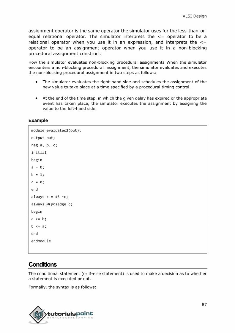
VLSI Design
87
assignment operator is the same operator the simulator uses for the less-than-or-
equal relational operator. The simulator interprets the <= operator to be a
relational operator when you use it in an expression, and interprets the <=
operator to be an assignment operator when you use it in a non-blocking
procedural assignment construct.
How the simulator evaluates non-blocking procedural assignments When the simulator
encounters a non-blocking procedural assignment, the simulator evaluates and executes
the non-blocking procedural assignment in two steps as follows:
The simulator evaluates the right-hand side and schedules the assignment of the
new value to take place at a time specified by a procedural timing control.
At the end of the time step, in which the given delay has expired or the appropriate
event has taken place, the simulator executes the assignment by assigning the
value to the left-hand side.
Example
module evaluates2(out);
output out;
reg a, b, c;
initial
begin
a = 0;
b = 1;
c = 0;
end
always c = #5 ~c;
always @(posedge c)
begin
a <= b;
b <= a;
end
endmodule
Conditions
The conditional statement (or if-else statement) is used to make a decision as to whether
a statement is executed or not.
Formally, the syntax is as follows:

VLSI Design
88
<statement>
::= if ( <expression> ) <statement_or_null>
||= if ( <expression> ) <statement_or_null>
else <statement_or_null>
<statement_or_null>
::= <statement>
||= ;
The <expression> is evaluated; if it is true (that is, has a non-zero known value), the first
statement executes. If it is false (has a zero value or the value is x or z), the first statement
does not execute. If there is an else statement and <expression> is false, the else
statement executes. Since, the numeric value of the if expression is tested for being zero,
certain shortcuts are possible.
For example, the following two statements express the same logic:
if (expression)
if (expression != 0)
Since, the else part of an if-else is optional, there can be confusion when an else is omitted
from a nested if sequence. This is resolved by always associating the else with the closest
previous if that lacks an else.
Example
if (index > 0)
if (rega > regb)
result = rega;
else // else applies to preceding if
result = regb;
If that association is not what you want, use a begin-end block statement
to force the proper association
if (index > 0)
begin
if (rega > regb)
result = rega;
end
else
result = regb;
Construction of: if- else- if
The following construction occurs so often that it is worth a brief separate discussion.
VLSI Design
89
Example
if (<expression>)
<statement>
else if (<expression>)
<statement>
else if (<expression>)
<statement>
else
<statement>
This sequence of if’s (known as an if-else-if construct) is the most general way of writing
a multi-way decision. The expressions are evaluated in order; if any expression is true,
the statement associated with it is executed, and this terminates the whole chain. Each
statement is either a single statement or a block of statements.
The last else part of the if-else-if construct handles the ‘none of the above’ or default case
where none of the other conditions was satisfied. Sometimes there is no explicit action for
the default; in that case, the trailing else can be omitted or it can be used for error checking
to catch an impossible condition.
Case Statement
The case statement is a special multi-way decision statement that tests whether an
expression matches one of a number of other expressions, and branches accordingly. The
case statement is useful for describing, for example, the decoding of a microprocessor
instruction. The case statement has the following syntax:
Example
<statement>
::= case ( <expression> ) <case_item>+ endcase
||= casez ( <expression> ) <case_item>+ endcase
||= casex ( <expression> ) <case_item>+ endcase
<case_item>
::= <expression> <,<expression>>* : <statement_or_null>
||= default : <statement_or_null>
||= default <statement_or_null>
The case expressions are evaluated and compared in the exact order in which they are
given. During the linear search, if one of the case item expressions matches the expression
in parentheses, then the statement associated with that case item is executed. If all
comparisons fail, and the default item is given, then the default item statement is
executed. If the default statement is not given, and all of the comparisons fail, then none
of the case item statements is executed.
VLSI Design
90
Apart from syntax, the case statement differs from the multi-way if-else-if construct in
two important ways:
The conditional expressions in the if-else-if construct are more general than
comparing one expression with several others, as in the case statement.
The case statement provides a definitive result when there are x and z values in an
expression.
Looping Statements
There are four types of looping statements. They provide a means of controlling the
execution of a statement zero, one, or more times.
forever continuously executes a statement.
repeat executes a statement a fixed number of times.
while executes a statement until an expression becomes false. If the expression
starts out false, the statement is not executed at all.
for controls execution of its associated statement(s) by a three-step process, as
follows: o Executes an assignment normally used to initialize a variable that
controls the number of loops executed
o Evaluates an expression—if the result is zero, the for loop exits, and if it
is not zero, the for loop executes its associated statement(s) and then performs step 3
o Executes an assignment normally used to modify the value of the loop-
control variable, then repeats step 2
The following are the syntax rules for the looping statements:
Example:
<statement>
::= forever <statement>
||=forever
begin
<statement>+
end
<Statement>
::= repeat ( <expression> ) <statement>
||=repeat ( <expression> )
VLSI Design
91
begin
<statement>+
end
<statement>
::= while ( <expression> ) <statement>
||=while ( <expression> )
begin
<statement>+
end
<statement>
::= for ( <assignment> ; <expression> ; <assignment> )
<statement>
||=for ( <assignment> ; <expression> ; <assignment> )
begin
<statement>+
end
Delay Controls
Delay Control
The execution of a procedural statement can be delay-controlled by using the following
syntax:
<statement>
::= <delay_control> <statement_or_null>
<delay_control>
::= # <NUMBER>
||= # <identifier>
||= # ( <mintypmax_expression> )
The following example delays the execution of the assignment by 10 time units:
#10 rega = regb;
The next three examples provide an expression following the number sign (#). Execution
of the assignment delays by the amount of simulation time specified by the value of the
expression.
VLSI Design
92
Event Control
The execution of a procedural statement can be synchronized with a value change on a
net or register, or the occurrence of a declared event, by using the following event control
syntax:
Example
<statement>
::= <event_control> <statement_or_null>
<event_control>
::= @ <identifier>
||= @ ( <event_expression> )
<event_expression>
::= <expression>
||= posedge <SCALAR_EVENT_EXPRESSION>
||= negedge <SCALAR_EVENT_EXPRESSION>
||= <event_expression> <or <event_expression>>
*<SCALAR_EVENT_EXPRESSION> is an expression that resolves to a one bit value.
Value changes on nets and registers can be used as events to trigger the execution of a
statement. This is known as detecting an implicit event. Verilog syntax also allows you to
detect change based on the direction of the change—that is, toward the value 1 (posedge)
or toward the value 0 (negedge). The behaviour of posedge and negedge for unknown
expression values is as follows:
a negedge is detected on the transition from 1 to unknown and from unknown to 0
a posedge is detected on the transition from 0 to unknown and from unknown to 1
Procedures: Always and Initial Blocks
All procedures in Verilog are specified within one of the following four Blocks. 1) Initial
blocks 2) Always blocks 3) Task 4) Function
The initial and always statements are enabled at the beginning of simulation. The initial
blocks executes only once and its activity dies when the statement has finished. In
contrast, the always blocks executes repeatedly. Its activity dies only when the simulation
is terminated. There is no limit to the number of initial and always blocks that can be
defined in a module. Tasks and functions are procedures that are enabled from one or
more places in other procedures.
VLSI Design
93
Initial Blocks
The syntax for the initial statement is as follows:
<initial_statement>
::= initial <statement>
The following example illustrates the use of the initial statement for initialization of
variables at the start of simulation.
Initial
Begin
Areg = 0; // initialize a register
For (index = 0; index < size; index = index + 1)
Memory [index] = 0; //initialize a memory
Word
End
Another typical usage of the initial Blocks is specification of waveform descriptions that
execute once to provide stimulus to the main part of the circuit being simulated.
Initial
Begin
Inputs = ’b000000;
// initialize at time zero
#10 inputs = ’b011001; // first pattern
#10 inputs = ’b011011; // second pattern
#10 inputs = ’b011000; // third pattern
#10 inputs = ’b001000; // last pattern
End
Always Blocks
The ‘always’ statement repeats continuously throughout the whole simulation run. The
syntax for the always statement is given below
<always_statement>
::= always <statement>
The ‘always’ statement, because of its looping nature, is only useful when used in
conjunction with some form of timing control. If an ‘always’ statement provides no means
for time to advance, the ‘always’ statement creates a simulation deadlock condition. The
following code, for example, creates an infinite zero-delay loop:
Always areg = ~areg;

VLSI Design
94
Providing a timing control to the above code creates a potentially useful description—as in
the following example:
Always #half_period areg = ~areg;