Slide 1
Microblaze Performance Monitoring Engine
Alex BurnsECE 631
April 25, 2005

Slide 2
Outline
• Project description
• Microblaze performance
• Xilinx tools overview
• Microblaze implementation
• Performance monitoring
• Stream processing engine
• Implementation results

Slide 3
Description
• Implement a Microblaze soft processor
• Use a Virtex 2 Pro evaluation board
• Connect a performance monitoring engine to relevant signals of the processor

Slide 4
Microblaze Core Diagram
Processor CoreMemory Interface Memory Interface
Slide 5
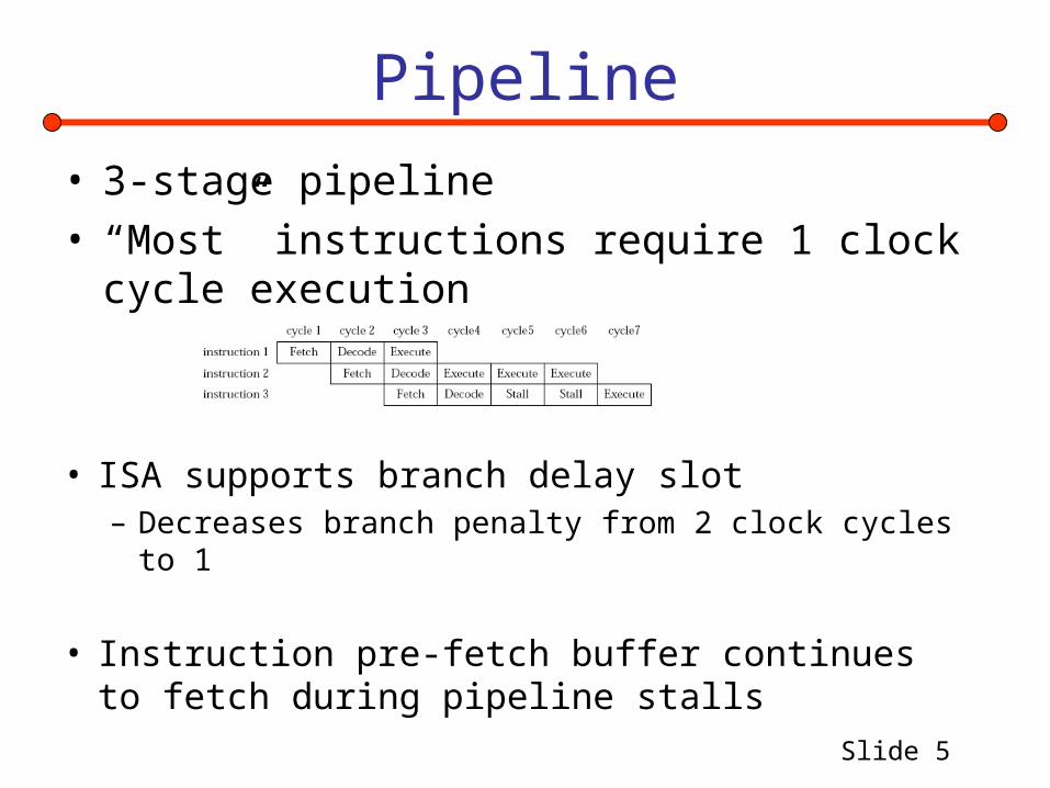
Pipeline
• 3-stage pipeline• “Most” instructions require 1 clock cycle
execution
• ISA supports branch delay slot – Decreases branch penalty from 2 clock cycles to 1
• Instruction pre-fetch buffer continues to fetch during pipeline stalls
Slide 6
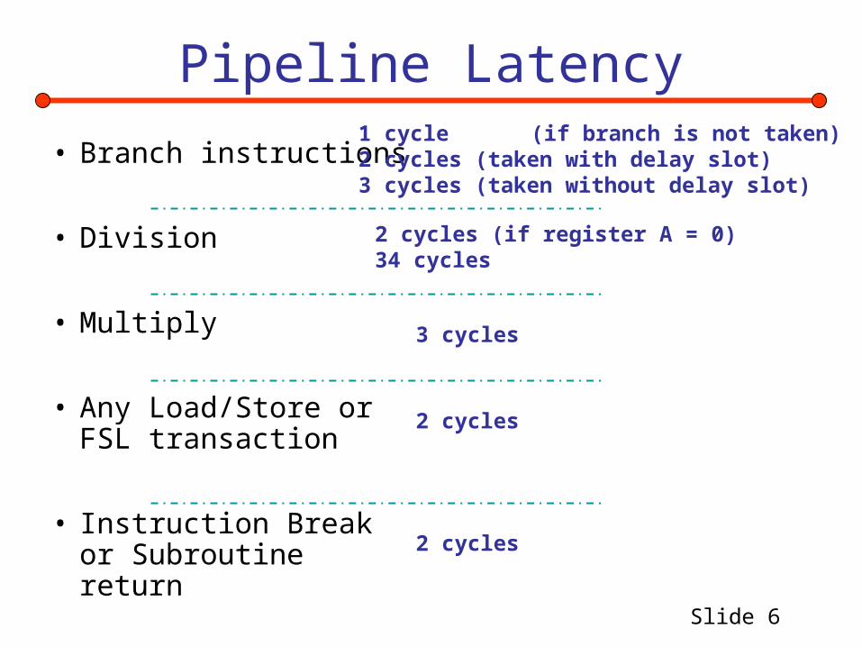
Pipeline Latency
• Branch instructions
• Division
• Multiply
• Any Load/Store or FSL transaction
• Instruction Break or Subroutine return
1 cycle (if branch is not taken)2 cycles (taken with delay slot) 3 cycles (taken without delay slot)
2 cycles (if register A = 0)34 cycles
3 cycles
2 cycles
2 cycles

Slide 7
Performance• Soft architecture trades configurability for limited
performance
• Due to limited performance, software optimization offers great potential
• Need to monitor software algorithms for efficiency to achieve the most performance for a given logic area
• Logic could be added to improve performance– Designer must decide if this is necessary

Slide 8
Xilinx Platform StudioSystem DescriptionSystem Setup
Create system description files

Slide 9
System Creation 11. Use System Description (*.mhs) to generate a Netlist
2. Setup project hierarchy as microblaze is a submodule to a Xilinx Project Navigator entity
3. Create Board Support Libraries for given system description
4. Create HDL using Project Navigator to attach logic system description
5. Perform Synthesis, Mapping, Place and Route, Bit File creation using Project Navigator

Slide 10
System Creation 26. Return to Platform Studio to attach compiled software to bitstream
7. Load bitstream to FPGA
8. Attach Xilinx debugger (XMD) through JTAG port and attach process to configured Microblaze within FPGA
9. Load compiled software into instruction memory using XMD
10. Cross fingers
11. Run code

Slide 11
Project Goal 1
• Implement a Microblaze– Synthesized all logic– Mapped to Memec evaluation board
containing a Virtex 2 Pro (XCS2VP4)– Successfully ran test program which tests all
IO, memory and displays output through UART

Slide 12
Performance Monitoring Plan
• Detect cache parameters for given algorithm
– Monitor Instruction side memory bus for accesses
– Store accesses into VHDL counter
– Read counter upon completion of micro-benchmark

Slide 13
Cache Operation
1. Detect if address is cacheable
2. If cacheable, lookup in tag memory
3. If tag matches and valid bit is set, drive the ready signal (Cache Hit)
• On cache miss, the cache waits for the OPB to fetch the data from memory
– does not assert ready signal

Slide 14
Trace Interface
The geniuses at Xilinx already thought of the need to monitor performance of
the configurable Microblaze

Slide 15
New Project Goal 2
• Use given performance monitoring tools to connect to Stream Processing Engine

Slide 16
What is a Stream
• A stream is a block of instructions stored consecutively in memory and executed without branches
for (i=0; i<30; i++) a += c[i];
Initialize
Execute
Terminate
Stream 1Stream 2
Stream 3
Functional Blocks Streams

Slide 17
Stream Processor
Stream Processor Stream Collector
Detector
FIFO
Hash Table
IDIDValid
NewStreamValid
Start Address
Length
ClockReset
PC

Slide 18
System Outline

Slide 19
Design Steps
• Develop UART– Modified an existing design from
Opencores.org– Runs at 115K baud– Transmitter only
• Connected UART to Stream Processor output

Slide 20
Status
• Working Microblaze running board test software– Software could be easily changed to any
microbenchmark
• Working Stream Processor
• Working UART

Slide 21
Design Problems
• Microblaze requires 26 block rams with selected configuration
• Stream Processor requires 39 block rams due to enormous hash table (4K x 49) and other FIFOs (8 x 48)
• Available V2Pro FPGA contains 28 block rams and no external ram

Slide 22
Design Mitigation
• Decrease hash table within FPGA by not storing entire PC
• Decrease hash table by shortening maximum stream length to be detected
• Removed cache in Microblaze
• 28 required Block Rams now fit into FPGA

Slide 23
More Problems
• Branch occurs every 8 instructions on average
• Microblaze runs at 100MHz
• UART runs at 115K with ascii data requiring 10 bits per character (with start and stop bits)
Slide 24
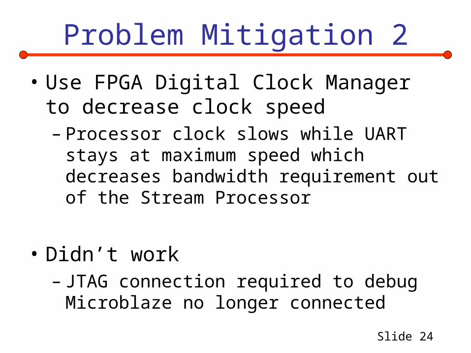
Problem Mitigation 2
• Use FPGA Digital Clock Manager to decrease clock speed– Processor clock slows while UART stays at
maximum speed which decreases bandwidth requirement out of the Stream Processor
• Didn’t work– JTAG connection required to debug
Microblaze no longer connected

Slide 25
Future Work
• Use a much higher bandwidth communication link to send data out of the stream processor– IDT FIFO, external memory, USB, Ethernet
• Use an FPGA with more available BRAMs to avoid performance hit in stream hash table

Slide 26
Questions
Recommended