HDL Compiler™
for Verilog User GuideVersion F-2011.09-SP4, March 2012
Copyright Notice and Proprietary InformationCopyright © 2012 Synopsys, Inc. All rights reserved. This software and documentation contain confidential and proprietary information that is the property of Synopsys, Inc. The software and documentation are furnished under a license agreement and may be used or copied only in accordance with the terms of the license agreement. No part of the software and documentation may be reproduced, transmitted, or translated, in any form or by any means, electronic, mechanical, manual, optical, or otherwise, without prior written permission of Synopsys, Inc., or as expressly provided by the license agreement.
Destination Control StatementAll technical data contained in this publication is subject to the export control laws of the United States of America. Disclosure to nationals of other countries contrary to United States law is prohibited. It is the reader s responsibility to determine the applicable regulations and to comply with them.
DisclaimerSYNOPSYS, INC., AND ITS LICENSORS MAKE NO WARRANTY OF ANY KIND, EXPRESS OR IMPLIED, WITH REGARD TO THIS MATERIAL, INCLUDING, BUT NOT LIMITED TO, THE IMPLIED WARRANTIES OF MERCHANTABILITY AND FITNESS FOR A PARTICULAR PURPOSE.
Registered Trademarks (®)Synopsys, AEON, AMPS, ARC, Astro, Behavior Extracting Synthesis Technology, Cadabra, CATS, Certify, CHIPit, CODE V, CoMET, Confirma, Design Compiler, DesignSphere, DesignWare, Eclypse, Formality, Galaxy Custom Designer, Global Synthesis, HAPS, HapsTrak, HDL Analyst, HSIM, HSPICE, Identify, Leda, LightTools, MAST, MaVeric, METeor, ModelTools, NanoSim, NOVeA, OpenVera, ORA, PathMill, Physical Compiler, PrimeTime, SCOPE, SiVL, SNUG, SolvNet, Sonic Focus, STAR Memory System, SVP Café, Syndicated, Synplicity, Synplify, Synplify Pro, Synthesis Constraints Optimization Environment, TetraMAX, the Synplicity logo, UMRBus, VCS, Vera, and YieldExplorer are registered trademarks of Synopsys, Inc.
Trademarks (™)AFGen, Apollo, ASAP, Astro-Rail, Astro-Xtalk, Aurora, AvanWaves, BEST, Columbia, Columbia-CE, Cosmos, CosmosLE, CosmosScope, CRITIC, Custom WaveView, CustomExplorer, CustomSim, DC Expert, DC Professional, DC Ultra, Design Analyzer, Design Vision, DesignerHDL, DesignPower, DFTMAX, Direct Silicon Access, Discovery, Encore, EPIC, Galaxy, HANEX, HDL Compiler, Hercules, Hierarchical Optimization Technology, High-performance ASIC Prototyping
System, HSIMplus
, i-Virtual Stepper, IC Compiler, IICE, in-Sync, iN-Tandem, Intelli, Jupiter, Jupiter-DP, JupiterXT, JupiterXT-ASIC, Liberty, Libra-Passport, Library Compiler, Macro-PLUS, Magellan, Mars, Mars-Rail, Mars-Xtalk, Milkyway, ModelSource, Module Compiler, MultiPoint, ORAengineering, Physical Analyst, Planet, Planet-PL, Platform Architect, Polaris, Power Compiler, Processor Designer, Raphael, RippledMixer, Saturn, Scirocco, Scirocco-i, SiWare, SPW, Star-RCXT, Star-SimXT, StarRC, Synphony Model System Compiler, System Compiler, System Designer, System Studio, Taurus, TotalRecall, TSUPREM-4, VCSi, VHDL Compiler, VMC, and Worksheet Buffer are trademarks of Synopsys, Inc.
Service Marks (SM)MAP-in and TAP-in are service marks of Synopsys, Inc.
Third Party Trademark AcknowledgementsSystemC is a trademark of the Open SystemC Initiative and is used under license.ARM and AMBA are registered trademarks of ARM Limited.Saber is a registered trademark of SabreMark Limited Partnership and is used under license.Entrust is a registered trademark of Entrust Inc. in the United States and in certain other countries. In Canada, Entrust is a trademark or registered trademark of Entrust Technologies Limited. Used by Entrust.net Inc. under license.All other product or company names may be trademarks of their respective owners.
Synopsys, Inc.700 E. Middlefield RoadMountain View, CA 94043www.synopsys.com
HDL Compiler for Verilog User Guide, version F-2011.09-SP4 ii

Copyright Statement for the Command-Line Editing FeatureCopyright © 1992, 1993 The Regents of the University of California. All rights reserved. This code is derived from software contributed to Berkeley by Christos Zoulas of Cornell University.
Redistribution and use in source and binary forms, with or without modification, are permitted provided that the following conditions are met:1. Redistributions of source code must retain the above copyright notice, this list of conditions and the following disclaimer.2. Redistributions in binary form must reproduce the above copyright notice, this list of conditions and the following disclaimer in the documentation and/or other materials provided with the distribution.3. All advertising materials mentioning features or use of this software must display the following acknowledgement:This product includes software developed by the University of California, Berkeley and its contributors.4. Neither the name of the University nor the names of its contributors may be used to endorse or promote products derived from this software without specific prior written permission.
THIS SOFTWARE IS PROVIDED BY THE REGENTS AND CONTRIBUTORS "AS IS" AND ANY EXPRESS OR IMPLIED WARRANTIES, INCLUDING, BUT NOT LIMITED TO, THE IMPLIED WARRANTIES OF MERCHANTABILITY AND FITNESS FOR A PARTICULAR PURPOSE ARE DISCLAIMED. IN NO EVENT SHALL THE REGENTS OR CONTRIBUTORS BE LIABLE FOR ANY DIRECT, INDIRECT, INCIDENTAL, SPECIAL, EXEMPLARY, OR CONSEQUENTIAL DAMAGES (INCLUDING, BUT NOT LIMITED TO, PROCUREMENT OF SUBSTITUTE GOODS OR SERVICES; LOSS OF USE, DATA, OR PROFITS; OR BUSINESS INTERRUPTION) HOWEVER CAUSED AND ON ANY THEORY OF LIABILITY, WHETHER IN CONTRACT, STRICT LIABILITY, OR TORT (INCLUDING NEGLIGENCE OR OTHERWISE) ARISING IN ANY WAY OUT OF THE USE OF THIS SOFTWARE, EVEN IF ADVISED OF THE POSSIBILITY OF SUCH DAMAGE.
Copyright Statement for the Line-Editing LibraryCopyright © 1992 Simmule Turner and Rich Salz. All rights reserved.
This software is not subject to any license of the American Telephone and Telegraph Company or of the Regents of the University of California.
Permission is granted to anyone to use this software for any purpose on any computer system, and to alter it and redistribute it freely, subject to the following restrictions: 1. The authors are not responsible for the consequences of use of this software, no matter how awful, even if they arise from flaws in it. 2. The origin of this software must not be misrepresented, either by explicit claim or by omission. Since few users ever read sources, credits must appear in the documentation. 3. Altered versions must be plainly marked as such, and must not be misrepresented as being the original software. Since few users ever read sources, credits must appear in the documentation. 4. This notice may not be removed or altered.
HDL Compiler for Verilog User Guide, version F-2011.09-SP4 iii

HDL Compiler for Verilog User Guide, version F-2011.09-SP4 iv

Contents
About This Manual . . . . . . . . . . . . . . . . . . . . . . . . . . . . . . . . . . . . . . . . . . . . . . . . . . xiv
Customer Support. . . . . . . . . . . . . . . . . . . . . . . . . . . . . . . . . . . . . . . . . . . . . . . . . . . xvii
1. Introduction to HDL Compiler for Verilog
Reading Verilog Designs . . . . . . . . . . . . . . . . . . . . . . . . . . . . . . . . . . . . . . . . . . . . . 1-3
Reading Designs With Dependencies Automatically . . . . . . . . . . . . . . . . . . . . . 1-3Reading, Analyzing, and Elaborating Designs . . . . . . . . . . . . . . . . . . . . . . 1-3Reading and Analyzing Designs Without Elaboration . . . . . . . . . . . . . . . . 1-4File Dependency Support . . . . . . . . . . . . . . . . . . . . . . . . . . . . . . . . . . . . . . 1-5Supported Variables . . . . . . . . . . . . . . . . . . . . . . . . . . . . . . . . . . . . . . . . . . 1-6Examples . . . . . . . . . . . . . . . . . . . . . . . . . . . . . . . . . . . . . . . . . . . . . . . . . . 1-6
Automatic Detection of RTL Language From File Extensions . . . . . . . . . . . . . . 1-7
Controlling the Verilog Version Used for Reading RTL Files . . . . . . . . . . . . . . . 1-7
Elaboration Reports . . . . . . . . . . . . . . . . . . . . . . . . . . . . . . . . . . . . . . . . . . . . . . . . . 1-7
Reporting Elaboration Errors . . . . . . . . . . . . . . . . . . . . . . . . . . . . . . . . . . . . . . . . . . 1-9
Methodology . . . . . . . . . . . . . . . . . . . . . . . . . . . . . . . . . . . . . . . . . . . . . . . . . . . 1-10
Examples . . . . . . . . . . . . . . . . . . . . . . . . . . . . . . . . . . . . . . . . . . . . . . . . . . . . . . 1-10
Netlist Reader . . . . . . . . . . . . . . . . . . . . . . . . . . . . . . . . . . . . . . . . . . . . . . . . . . . . . . 1-16
Automatic Detection of Input Type . . . . . . . . . . . . . . . . . . . . . . . . . . . . . . . . . . . . . . 1-16
Reading In Designs . . . . . . . . . . . . . . . . . . . . . . . . . . . . . . . . . . . . . . . . . . . . . . . . . 1-17
Defining Macros . . . . . . . . . . . . . . . . . . . . . . . . . . . . . . . . . . . . . . . . . . . . . . . . . . . . 1-17
Using analyze -define . . . . . . . . . . . . . . . . . . . . . . . . . . . . . . . . . . . . . . . . . . . . 1-17
Predefined Macros . . . . . . . . . . . . . . . . . . . . . . . . . . . . . . . . . . . . . . . . . . . . . . 1-18
v
HDL Compiler for Verilog User Guide F-2011.09-SP4HDL Compiler for Verilog User Guide Version F-2011.09-SP4
Global Macro Reset: `undefineall . . . . . . . . . . . . . . . . . . . . . . . . . . . . . . . . . . . 1-18
Parameterized Designs. . . . . . . . . . . . . . . . . . . . . . . . . . . . . . . . . . . . . . . . . . . . . . . 1-19
Reading Large Designs . . . . . . . . . . . . . . . . . . . . . . . . . . . . . . . . . . . . . . . . . . . . . . 1-20
Use of $display During RTL Elaboration. . . . . . . . . . . . . . . . . . . . . . . . . . . . . . . . . . 1-21
Inputs and Outputs . . . . . . . . . . . . . . . . . . . . . . . . . . . . . . . . . . . . . . . . . . . . . . . . . . 1-22
Input Descriptions . . . . . . . . . . . . . . . . . . . . . . . . . . . . . . . . . . . . . . . . . . . . . . . 1-23
Design Hierarchy . . . . . . . . . . . . . . . . . . . . . . . . . . . . . . . . . . . . . . . . . . . . . . . . 1-25
Component Inference and Instantiation. . . . . . . . . . . . . . . . . . . . . . . . . . . . . . . 1-25
Naming Considerations . . . . . . . . . . . . . . . . . . . . . . . . . . . . . . . . . . . . . . . . . . . 1-25
Generic Netlists . . . . . . . . . . . . . . . . . . . . . . . . . . . . . . . . . . . . . . . . . . . . . . . . 1-26
Inference Reports . . . . . . . . . . . . . . . . . . . . . . . . . . . . . . . . . . . . . . . . . . . . . . . 1-29
Error Messages . . . . . . . . . . . . . . . . . . . . . . . . . . . . . . . . . . . . . . . . . . . . . . . . . 1-29
Language Construct Support . . . . . . . . . . . . . . . . . . . . . . . . . . . . . . . . . . . . . . . . . . 1-29
Licenses . . . . . . . . . . . . . . . . . . . . . . . . . . . . . . . . . . . . . . . . . . . . . . . . . . . . . . . . . . 1-30
2. Coding Considerations
Coding for QoR. . . . . . . . . . . . . . . . . . . . . . . . . . . . . . . . . . . . . . . . . . . . . . . . . . . . . 2-2
Creating Relative Placement in Hardware Description Languages . . . . . . . . . . . . . 2-2
Support for Relative Placement . . . . . . . . . . . . . . . . . . . . . . . . . . . . . . . . . . . . 2-3
Directives for Specifying Relative Placement. . . . . . . . . . . . . . . . . . . . . . . . . . . 2-4
Creating Groups Using `rp_group and `rp_endgroup . . . . . . . . . . . . . . . . . . . . 2-4
Specifying Subgroups, Keepouts, and Instances Using `rp_place . . . . . . . . . . 2-5
Placing Cells Automatically Using `rp_fill. . . . . . . . . . . . . . . . . . . . . . . . . . . . . . 2-6
Specifying Placement for Array Elements Using `rp_array_dir . . . . . . . . . . . . . 2-8
Specifying Cell Alignment Using rp_align . . . . . . . . . . . . . . . . . . . . . . . . . . . . . 2-8
Specifying Cell Orientation Using rp_orient. . . . . . . . . . . . . . . . . . . . . . . . . . . . 2-9
Ignoring Relative Placement Using rp_ignore and rp_endignore . . . . . . . . . . . 2-10
Relative Placement Examples . . . . . . . . . . . . . . . . . . . . . . . . . . . . . . . . . . . . . . 2-10
General Coding Guidelines. . . . . . . . . . . . . . . . . . . . . . . . . . . . . . . . . . . . . . . . . . . . 2-16
Separate Sequential and Combinational Assignments . . . . . . . . . . . . . . . . . . . 2-17
Persistence of Values Across Calls to Tasks . . . . . . . . . . . . . . . . . . . . . . . . . . 2-17
defparam . . . . . . . . . . . . . . . . . . . . . . . . . . . . . . . . . . . . . . . . . . . . . . . . . . . . . . 2-18
Function Placed Within a Module . . . . . . . . . . . . . . . . . . . . . . . . . . . . . . . . . . . 2-18
Contents vi
HDL Compiler for Verilog User Guide Version F-2011.09-SP4
Interacting With Other Flows. . . . . . . . . . . . . . . . . . . . . . . . . . . . . . . . . . . . . . . . . . . 2-18
Synthesis Flows. . . . . . . . . . . . . . . . . . . . . . . . . . . . . . . . . . . . . . . . . . . . . . . . . 2-18Controlling Structure With Parentheses . . . . . . . . . . . . . . . . . . . . . . . . . . . 2-19Multibit Components . . . . . . . . . . . . . . . . . . . . . . . . . . . . . . . . . . . . . . . . . 2-19
Low-Power Flows. . . . . . . . . . . . . . . . . . . . . . . . . . . . . . . . . . . . . . . . . . . . . . . . 2-19Keeping Signal Names . . . . . . . . . . . . . . . . . . . . . . . . . . . . . . . . . . . . . . . . 2-19
Verification Flows. . . . . . . . . . . . . . . . . . . . . . . . . . . . . . . . . . . . . . . . . . . . . . . . 2-22Simulation/Synthesis Mismatch Issues. . . . . . . . . . . . . . . . . . . . . . . . . . . . 2-22
3. Modeling Combinational Logic
Synthetic Operators . . . . . . . . . . . . . . . . . . . . . . . . . . . . . . . . . . . . . . . . . . . . . . . . . 3-2
Logic and Arithmetic Expressions. . . . . . . . . . . . . . . . . . . . . . . . . . . . . . . . . . . . . . . 3-4
Basic Operators . . . . . . . . . . . . . . . . . . . . . . . . . . . . . . . . . . . . . . . . . . . . . . . . . 3-4
Carry-Bit Overflow . . . . . . . . . . . . . . . . . . . . . . . . . . . . . . . . . . . . . . . . . . . . . . 3-5
Divide Operators . . . . . . . . . . . . . . . . . . . . . . . . . . . . . . . . . . . . . . . . . . . . . . . . 3-6
Sign Conversions . . . . . . . . . . . . . . . . . . . . . . . . . . . . . . . . . . . . . . . . . . . . . . . 3-7
Multiplexing Logic . . . . . . . . . . . . . . . . . . . . . . . . . . . . . . . . . . . . . . . . . . . . . . . . . . . 3-12
SELECT_OP Inference . . . . . . . . . . . . . . . . . . . . . . . . . . . . . . . . . . . . . . . . . . . 3-13
One-Hot Multiplexer Inference . . . . . . . . . . . . . . . . . . . . . . . . . . . . . . . . . . . . . . 3-14
MUX_OP Inference . . . . . . . . . . . . . . . . . . . . . . . . . . . . . . . . . . . . . . . . . . . . . . 3-15
Variables That Control MUX_OP Inference . . . . . . . . . . . . . . . . . . . . . . . . . . . . 3-17MUX_OP Inference Examples . . . . . . . . . . . . . . . . . . . . . . . . . . . . . . . . . . 3-18
Considerations When Using If Statements to Code For MUX_OPs . . . . . . . . 3-22
MUX_OP Inference Limitations . . . . . . . . . . . . . . . . . . . . . . . . . . . . . . . . . . . . . 3-25
MUX_OP Components With Variable Indexing. . . . . . . . . . . . . . . . . . . . . . . . . . . . . 3-26
Modeling Complex MUX Inferences: Bit and Memory Accesses. . . . . . . . . . . . . . . 3-26
Bit-Truncation Coding for DC Ultra Datapath Extraction . . . . . . . . . . . . . . . . . . . . . . 3-27
Latches in Combinational Logic . . . . . . . . . . . . . . . . . . . . . . . . . . . . . . . . . . . . . . . . 3-30
4. Modeling Sequential Logic
Generic Sequential Cells (SEQGENs) . . . . . . . . . . . . . . . . . . . . . . . . . . . . . . . . . . . 4-2
Inference Reports for Registers . . . . . . . . . . . . . . . . . . . . . . . . . . . . . . . . . . . . . . . . 4-5
Register Inference Guidelines. . . . . . . . . . . . . . . . . . . . . . . . . . . . . . . . . . . . . . . . . . 4-6
Multiple Events in an always Block . . . . . . . . . . . . . . . . . . . . . . . . . . . . . . . . . . 4-6
Chapter 1: Contents 1-vii
Contents vii
HDL Compiler for Verilog User Guide F-2011.09-SP4HDL Compiler for Verilog User Guide Version F-2011.09-SP4
Minimizing Registers . . . . . . . . . . . . . . . . . . . . . . . . . . . . . . . . . . . . . . . . . . . . . 4-7
Keeping Unloaded Registers . . . . . . . . . . . . . . . . . . . . . . . . . . . . . . . . . . . . . . 4-9
Preventing Unwanted Latches: hdlin_check_no_latch. . . . . . . . . . . . . . . . . . . . 4-12
Register Inference Limitations . . . . . . . . . . . . . . . . . . . . . . . . . . . . . . . . . . . . . . 4-13
Register Inference Examples . . . . . . . . . . . . . . . . . . . . . . . . . . . . . . . . . . . . . . . . . . 4-14
Inferring Latches . . . . . . . . . . . . . . . . . . . . . . . . . . . . . . . . . . . . . . . . . . . . . . . . 4-14Basic D Latch . . . . . . . . . . . . . . . . . . . . . . . . . . . . . . . . . . . . . . . . . . . . . . . 4-14D Latch With Asynchronous Reset: Use async_set_reset . . . . . . . . . . . . . 4-15D Latch With Asynchronous Set and Reset: Use hdlin_latch_always_async_set_reset . . . . . . . . . . . . . . . . . . . . . . . . . 4-15
Inferring Flip-Flops. . . . . . . . . . . . . . . . . . . . . . . . . . . . . . . . . . . . . . . . . . . . . . . 4-16Basic D Flip-Flop . . . . . . . . . . . . . . . . . . . . . . . . . . . . . . . . . . . . . . . . . . . . 4-18D Flip-Flop With Asynchronous Reset Using ?: Construct . . . . . . . . . . . . . 4-18D Flip-Flop With Asynchronous Reset . . . . . . . . . . . . . . . . . . . . . . . . . . . . 4-19D Flip-Flop With Asynchronous Set and Reset . . . . . . . . . . . . . . . . . . . . . 4-19D Flip-Flop With Synchronous Reset: Use sync_set_reset . . . . . . . . . . . . . . . . . . . . . . . . . . . . . . . . . . . . . . . . . . 4-20D Flip-Flop With Synchronous and Asynchronous Load . . . . . . . . . . . . . . 4-20D Flip-Flops With Complex Set/Reset Signals . . . . . . . . . . . . . . . . . . . . . . 4-21Multiple Flip-Flops With Asynchronous and Synchronous Controls . . . . . . . . . . . . . . . . . . . . . . . . . . . . . . . . . . . . . . . . 4-23
5. Modeling Finite State Machines
FSM Coding Requirements for Automatic Inference. . . . . . . . . . . . . . . . . . . . . . . . . 5-2
FSM Inference Variables . . . . . . . . . . . . . . . . . . . . . . . . . . . . . . . . . . . . . . . . . . . . . 5-3
FSM Coding Example. . . . . . . . . . . . . . . . . . . . . . . . . . . . . . . . . . . . . . . . . . . . . . . . 5-3
FSM Inference Report . . . . . . . . . . . . . . . . . . . . . . . . . . . . . . . . . . . . . . . . . . . . . . . 5-5
Enumerated Types . . . . . . . . . . . . . . . . . . . . . . . . . . . . . . . . . . . . . . . . . . . . . . . . . . 5-6
6. Modeling Three-State Buffers
Using z Values . . . . . . . . . . . . . . . . . . . . . . . . . . . . . . . . . . . . . . . . . . . . . . . . . . . . . 6-2
Three-State Driver Inference Report . . . . . . . . . . . . . . . . . . . . . . . . . . . . . . . . . . . . 6-2
Assigning a Single Three-State Driver to a Single Variable . . . . . . . . . . . . . . . . . . . 6-3
Assigning Multiple Three-State Drivers to a Single Variable. . . . . . . . . . . . . . . . . . . 6-4
Registering Three-State Driver Data . . . . . . . . . . . . . . . . . . . . . . . . . . . . . . . . . . . . 6-5
Contents viii

HDL Compiler for Verilog User Guide Version F-2011.09-SP4
Instantiating Three-State Drivers . . . . . . . . . . . . . . . . . . . . . . . . . . . . . . . . . . . . . . . 6-6
Errors and Warnings . . . . . . . . . . . . . . . . . . . . . . . . . . . . . . . . . . . . . . . . . . . . . . . . . 6-6
7. HDL Compiler Synthesis Directives
async_set_reset . . . . . . . . . . . . . . . . . . . . . . . . . . . . . . . . . . . . . . . . . . . . . . . . . . . . 7-3
async_set_reset_local . . . . . . . . . . . . . . . . . . . . . . . . . . . . . . . . . . . . . . . . . . . . . . . 7-3
async_set_reset_local_all. . . . . . . . . . . . . . . . . . . . . . . . . . . . . . . . . . . . . . . . . . . . . 7-3
dc_tcl_script_begin and dc_tcl_script_end . . . . . . . . . . . . . . . . . . . . . . . . . . . . . . . . 7-4
enum . . . . . . . . . . . . . . . . . . . . . . . . . . . . . . . . . . . . . . . . . . . . . . . . . . . . . . . . . . . . 7-5
full_case . . . . . . . . . . . . . . . . . . . . . . . . . . . . . . . . . . . . . . . . . . . . . . . . . . . . . . . . . . 7-7
infer_multibit and dont_infer_multibit . . . . . . . . . . . . . . . . . . . . . . . . . . . . . . . . . . . . 7-9
Using the infer_multibit Directive . . . . . . . . . . . . . . . . . . . . . . . . . . . . . . . . . . . . 7-10
Using the dont_infer_multibit Directive . . . . . . . . . . . . . . . . . . . . . . . . . . . . . . . 7-11
Reporting Multibit Components . . . . . . . . . . . . . . . . . . . . . . . . . . . . . . . . . . . . 7-12
infer_mux . . . . . . . . . . . . . . . . . . . . . . . . . . . . . . . . . . . . . . . . . . . . . . . . . . . . . . . . . 7-14
infer_onehot_mux . . . . . . . . . . . . . . . . . . . . . . . . . . . . . . . . . . . . . . . . . . . . . . . . . . . 7-14
keep_signal_name . . . . . . . . . . . . . . . . . . . . . . . . . . . . . . . . . . . . . . . . . . . . . . . . . . 7-14
one_cold . . . . . . . . . . . . . . . . . . . . . . . . . . . . . . . . . . . . . . . . . . . . . . . . . . . . . . . . . 7-15
one_hot . . . . . . . . . . . . . . . . . . . . . . . . . . . . . . . . . . . . . . . . . . . . . . . . . . . . . . . . . . 7-15
parallel_case . . . . . . . . . . . . . . . . . . . . . . . . . . . . . . . . . . . . . . . . . . . . . . . . . . . . . . 7-15
preserve_sequential . . . . . . . . . . . . . . . . . . . . . . . . . . . . . . . . . . . . . . . . . . . . . . . . . 7-17
sync_set_reset . . . . . . . . . . . . . . . . . . . . . . . . . . . . . . . . . . . . . . . . . . . . . . . . . . . . . 7-17
sync_set_reset_local . . . . . . . . . . . . . . . . . . . . . . . . . . . . . . . . . . . . . . . . . . . . . . . . 7-17
sync_set_reset_local_all. . . . . . . . . . . . . . . . . . . . . . . . . . . . . . . . . . . . . . . . . . . . . . 7-18
template . . . . . . . . . . . . . . . . . . . . . . . . . . . . . . . . . . . . . . . . . . . . . . . . . . . . . . . . . . 7-19
translate_off and translate_on (Deprecated) . . . . . . . . . . . . . . . . . . . . . . . . . . . . . . 7-20
8. HDL Compiler Variables
HDL Compiler Reading-Related Variables . . . . . . . . . . . . . . . . . . . . . . . . . . . . . . . . 8-2
Commands for Writing Out Verilog . . . . . . . . . . . . . . . . . . . . . . . . . . . . . . . . . . . . . . 8-7
Chapter 1: Contents 1-ix
Contents ix
HDL Compiler for Verilog User Guide F-2011.09-SP4HDL Compiler for Verilog User Guide Version F-2011.09-SP4
Variables for Writing Out Verilog . . . . . . . . . . . . . . . . . . . . . . . . . . . . . . . . . . . . . . . . 8-7
Appendix A. Examples
Count Zeros—Combinational Version. . . . . . . . . . . . . . . . . . . . . . . . . . . . . . . . . . . . A-2
Count Zeros—Sequential Version. . . . . . . . . . . . . . . . . . . . . . . . . . . . . . . . . . . . . . . A-3
Drink Machine—State Machine Version . . . . . . . . . . . . . . . . . . . . . . . . . . . . . . . . . . A-5
Drink Machine—Count Nickels Version . . . . . . . . . . . . . . . . . . . . . . . . . . . . . . . . . . A-7
Carry-Lookahead Adder . . . . . . . . . . . . . . . . . . . . . . . . . . . . . . . . . . . . . . . . . . . . . . A-9
Coding for Late-Arriving Signals . . . . . . . . . . . . . . . . . . . . . . . . . . . . . . . . . . . . . . . . A-13
Datapath Duplication . . . . . . . . . . . . . . . . . . . . . . . . . . . . . . . . . . . . . . . . . . . . . A-13
Moving Late-Arriving Signals Closer to the Output . . . . . . . . . . . . . . . . . . . . . . A-16Overview. . . . . . . . . . . . . . . . . . . . . . . . . . . . . . . . . . . . . . . . . . . . . . . . . . . A-16Late-Arriving Data Signal . . . . . . . . . . . . . . . . . . . . . . . . . . . . . . . . . . . . . . A-18Recoding for Late-Arriving Data Signal: Case 1 . . . . . . . . . . . . . . . . . . . . . A-19Recoding for Late-Arriving Data Signal: Case 2 . . . . . . . . . . . . . . . . . . . . . A-21Late-Arriving Control Signal . . . . . . . . . . . . . . . . . . . . . . . . . . . . . . . . . . . . A-24Recoding for Late-Arriving Control Signal . . . . . . . . . . . . . . . . . . . . . . . . . A-25
Instantiation of Arrays of Instances . . . . . . . . . . . . . . . . . . . . . . . . . . . . . . . . . . . . . A-27
SR Latches . . . . . . . . . . . . . . . . . . . . . . . . . . . . . . . . . . . . . . . . . . . . . . . . . . . . . . . . A-30
D Latch With Asynchronous Set: Use async_set_reset . . . . . . . . . . . . . . . . . . . . . A-31
Inferring Master-Slave Latches . . . . . . . . . . . . . . . . . . . . . . . . . . . . . . . . . . . . . . . . . A-32
Master-Slave Latch Overview . . . . . . . . . . . . . . . . . . . . . . . . . . . . . . . . . . . . . . A-32
Master-Slave Latch With Single Master-Slave Clock Pair . . . . . . . . . . . . . . . . . A-32
Master-Slave Latch With Multiple Master-Slave Clock Pairs. . . . . . . . . . . . . . . . . . . . . . . . . . . . . . . . . . . . . . . . . . . . . . . . . . . . . . . . . . A-33
Master-Slave Latch With Discrete Components . . . . . . . . . . . . . . . . . . . . . . . . A-34
Inferring Flip-Flops . . . . . . . . . . . . . . . . . . . . . . . . . . . . . . . . . . . . . . . . . . . . . . . . . . A-35
D Flip-Flop With Synchronous Set: Use sync_set_reset . . . . . . . . . . . . . . . . . . . . . . . . . . . . . . . . . . . . . . . . . . . . . A-35
JK Flip-Flop With Synchronous Set and Reset: Use sync_set_reset . . . . . . . . . . . . . . . . . . . . . . . . . . . . . . . . . . . . . . . . . . . . . . A-36
Appendix B. Verilog Language Support
Syntax . . . . . . . . . . . . . . . . . . . . . . . . . . . . . . . . . . . . . . . . . . . . . . . . . . . . . . . . . . . B-2
Contents x

HDL Compiler for Verilog User Guide Version F-2011.09-SP4
Comments . . . . . . . . . . . . . . . . . . . . . . . . . . . . . . . . . . . . . . . . . . . . . . . . . . . . . B-2
Numbers . . . . . . . . . . . . . . . . . . . . . . . . . . . . . . . . . . . . . . . . . . . . . . . . . . . . . . B-2
Verilog Keywords . . . . . . . . . . . . . . . . . . . . . . . . . . . . . . . . . . . . . . . . . . . . . . . . . . . B-3
Unsupported Verilog Language Constructs . . . . . . . . . . . . . . . . . . . . . . . . . . . . . . . B-4
Construct Restrictions and Comments . . . . . . . . . . . . . . . . . . . . . . . . . . . . . . . . . . . B-5
always Blocks . . . . . . . . . . . . . . . . . . . . . . . . . . . . . . . . . . . . . . . . . . . . . . . . . . B-6
generate Statements . . . . . . . . . . . . . . . . . . . . . . . . . . . . . . . . . . . . . . . . . . . . . B-6Generate Overview. . . . . . . . . . . . . . . . . . . . . . . . . . . . . . . . . . . . . . . . . . . B-6Types of generate Blocks . . . . . . . . . . . . . . . . . . . . . . . . . . . . . . . . . . . . . . B-7Anonymous generate Blocks . . . . . . . . . . . . . . . . . . . . . . . . . . . . . . . . . . . B-7Loop Generate Blocks and Conditional Generate Blocks. . . . . . . . . . . . . . B-10Restrictions. . . . . . . . . . . . . . . . . . . . . . . . . . . . . . . . . . . . . . . . . . . . . . . . . B-11
Conditional Expressions (?:) Resource Sharing . . . . . . . . . . . . . . . . . . . . . . . . B-11
Case . . . . . . . . . . . . . . . . . . . . . . . . . . . . . . . . . . . . . . . . . . . . . . . . . . . . . . . . . B-11casez and casex . . . . . . . . . . . . . . . . . . . . . . . . . . . . . . . . . . . . . . . . . . . . B-12Full Case and Parallel Case . . . . . . . . . . . . . . . . . . . . . . . . . . . . . . . . . . . . B-12
defparam . . . . . . . . . . . . . . . . . . . . . . . . . . . . . . . . . . . . . . . . . . . . . . . . . . . . . . B-14
disable . . . . . . . . . . . . . . . . . . . . . . . . . . . . . . . . . . . . . . . . . . . . . . . . . . . . . . . B-14
Blocking and Nonblocking Assignments . . . . . . . . . . . . . . . . . . . . . . . . . . . . . . B-15
Macromodule . . . . . . . . . . . . . . . . . . . . . . . . . . . . . . . . . . . . . . . . . . . . . . . . . . . B-16
inout Port Declaration . . . . . . . . . . . . . . . . . . . . . . . . . . . . . . . . . . . . . . . . . . . . B-16
tri Data Type. . . . . . . . . . . . . . . . . . . . . . . . . . . . . . . . . . . . . . . . . . . . . . . . . . . . B-17
HDL Compiler Directives . . . . . . . . . . . . . . . . . . . . . . . . . . . . . . . . . . . . . . . . . . B-17`define. . . . . . . . . . . . . . . . . . . . . . . . . . . . . . . . . . . . . . . . . . . . . . . . . . . . . B-17`include . . . . . . . . . . . . . . . . . . . . . . . . . . . . . . . . . . . . . . . . . . . . . . . . . . . B-18`ifdef, `else, `endif, `ifndef, and `elsif. . . . . . . . . . . . . . . . . . . . . . . . . . . . . . B-19`rp_group and `rp_endgroup . . . . . . . . . . . . . . . . . . . . . . . . . . . . . . . . . . . B-20`rp_place. . . . . . . . . . . . . . . . . . . . . . . . . . . . . . . . . . . . . . . . . . . . . . . . . . . B-20`rp_fill . . . . . . . . . . . . . . . . . . . . . . . . . . . . . . . . . . . . . . . . . . . . . . . . . . . . . B-21`rp_array_dir . . . . . . . . . . . . . . . . . . . . . . . . . . . . . . . . . . . . . . . . . . . . . . . . B-21rp_align. . . . . . . . . . . . . . . . . . . . . . . . . . . . . . . . . . . . . . . . . . . . . . . . . . . . B-22rp_orient . . . . . . . . . . . . . . . . . . . . . . . . . . . . . . . . . . . . . . . . . . . . . . . . . . . B-22rp_ignore and rp_endignore . . . . . . . . . . . . . . . . . . . . . . . . . . . . . . . . . . . . B-23`undef . . . . . . . . . . . . . . . . . . . . . . . . . . . . . . . . . . . . . . . . . . . . . . . . . . . . . B-23
reg Types . . . . . . . . . . . . . . . . . . . . . . . . . . . . . . . . . . . . . . . . . . . . . . . . . . . . . . B-23
Types in Busing . . . . . . . . . . . . . . . . . . . . . . . . . . . . . . . . . . . . . . . . . . . . . . . . . B-23
Combinational while Loops . . . . . . . . . . . . . . . . . . . . . . . . . . . . . . . . . . . . . . . . B-24
Chapter 1: Contents 1-xi
Contents xi
HDL Compiler for Verilog User Guide F-2011.09-SP4HDL Compiler for Verilog User Guide Version F-2011.09-SP4
Verilog 2001 and 2005 Supported Constructs . . . . . . . . . . . . . . . . . . . . . . . . . . . . . B-27
Ignored Constructs . . . . . . . . . . . . . . . . . . . . . . . . . . . . . . . . . . . . . . . . . . . . . . . . . . B-29
Simulation Directives . . . . . . . . . . . . . . . . . . . . . . . . . . . . . . . . . . . . . . . . . . . . . B-29
Verilog System Functions . . . . . . . . . . . . . . . . . . . . . . . . . . . . . . . . . . . . . . . . . B-29
Verilog 2001 Feature Examples . . . . . . . . . . . . . . . . . . . . . . . . . . . . . . . . . . . . . . . . B-30
Multidimensional Arrays and Arrays of Nets . . . . . . . . . . . . . . . . . . . . . . . . . . . B-30
Signed Quantities . . . . . . . . . . . . . . . . . . . . . . . . . . . . . . . . . . . . . . . . . . . . . . . B-31
Comparisons With Signed Types. . . . . . . . . . . . . . . . . . . . . . . . . . . . . . . . . . . . B-33
Controlling Signs With Casting Operators . . . . . . . . . . . . . . . . . . . . . . . . . . . . . B-34
Part-Select Addressing Operators ([+:] and [-:]) . . . . . . . . . . . . . . . . . . . . . . . . B-35Variable Part-Select Overview . . . . . . . . . . . . . . . . . . . . . . . . . . . . . . . . . . B-35Example—Ascending Array and -: . . . . . . . . . . . . . . . . . . . . . . . . . . . . . . . B-36Example—Ascending Array and +:. . . . . . . . . . . . . . . . . . . . . . . . . . . . . . . B-37Example—Descending Array and the -: Operator . . . . . . . . . . . . . . . . . . . B-38Example—Descending Array and the +: Operator . . . . . . . . . . . . . . . . . . . B-39
Power Operator (**) . . . . . . . . . . . . . . . . . . . . . . . . . . . . . . . . . . . . . . . . . . . . . . B-40
Arithmetic Shift Operators (<<< and >>>) . . . . . . . . . . . . . . . . . . . . . . . . . . . . . B-40
Verilog 2005 Feature Example . . . . . . . . . . . . . . . . . . . . . . . . . . . . . . . . . . . . . . . . . B-41
Zero Replication. . . . . . . . . . . . . . . . . . . . . . . . . . . . . . . . . . . . . . . . . . . . . . . . . B-41
Glossary
Index
Contents xii
Preface
This preface includes the following sections:
• About This Manual
• Customer Support
xiii
HDL Compiler for Verilog User Guide F-2011.09-SP4HDL Compiler for Verilog User Guide Version F-2011.09-SP4
About This Manual
HDL Compiler translates a Verilog hardware language description into a generic technology (GTECH) netlist that is used by the Design Compiler tool to create an optimized netlist. This manual describes the following:
• Modeling combinational logic, synchronous logic, three-state buffers, and multibit cells with HDL Compiler for Verilog
• Sharing resources
• Using directives in the RTL
AudienceThe HDL Compiler for Verilog User Guide is written for logic designers and electronic engineers who are familiar with Design Compiler. Knowledge of the Verilog language is required, and knowledge of a high-level programming language is helpful.
Related PublicationsFor additional information about HDL Compiler, see the documentation on SolvNet at the following address:
https://solvnet.synopsys.com/DocsOnWeb
You might also want to see the documentation for the following related Synopsys products:
• Design Vision
• Design Compiler
• DesignWare
• Library Compiler
• Verilog Compiled Simulator (VCS)
Release NotesInformation about new features, changes, enhancements, known limitations, and resolved Synopsys Technical Action Requests (STARs) is available in the HDL Compiler Release Notes in SolvNet.
Preface About This Manual xiv

HDL Compiler for Verilog User Guide Version F-2011.09-SP4
To see the HDL Compiler Release Notes,
1. Go to the Download Center on SolvNet located at the following address:
https://solvnet.synopsys.com/DownloadCenter
2. Select HDL Compiler, and then select a release in the list that appears.
Chapter 1: Preface About This Manual 1-xvPreface About This Manual xv
HDL Compiler for Verilog User Guide F-2011.09-SP4HDL Compiler for Verilog User Guide Version F-2011.09-SP4
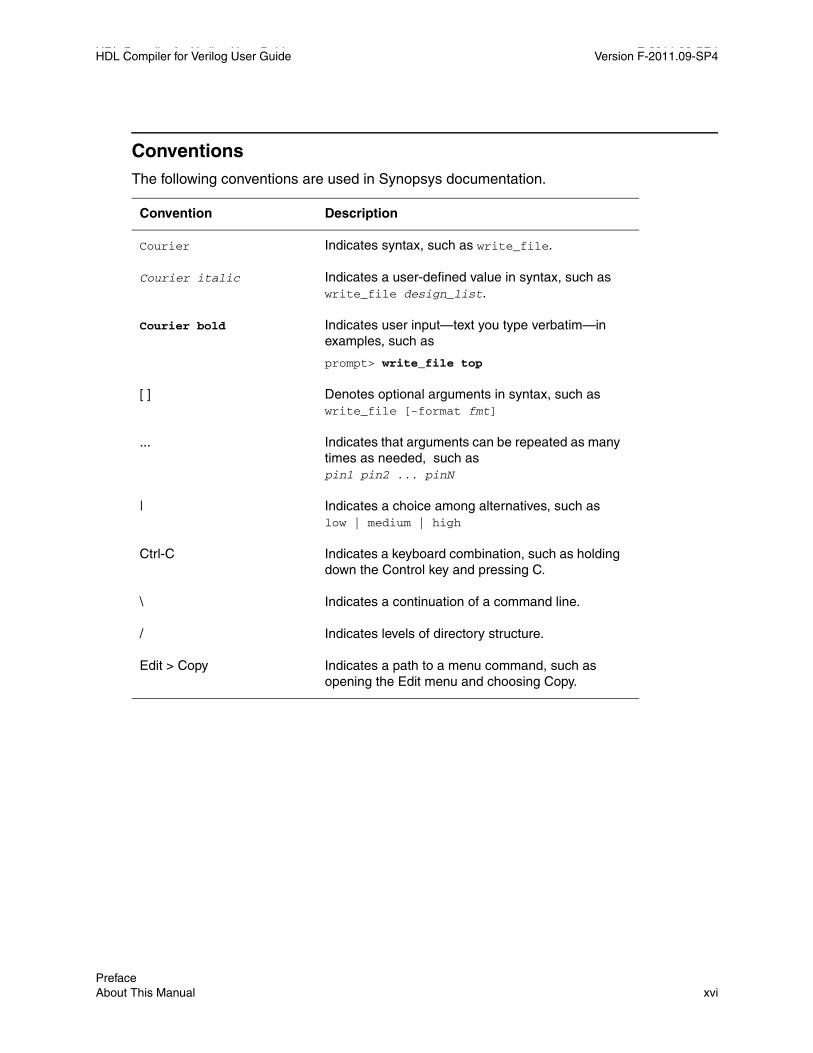
ConventionsThe following conventions are used in Synopsys documentation.
Convention Description
Courier Indicates syntax, such as write_file.
Courier italic Indicates a user-defined value in syntax, such as write_file design_list.
Courier bold Indicates user input—text you type verbatim—in examples, such as
prompt> write_file top
[ ] Denotes optional arguments in syntax, such as write_file [-format fmt]
... Indicates that arguments can be repeated as many times as needed, such as pin1 pin2 ... pinN
| Indicates a choice among alternatives, such as low | medium | high
Ctrl-C Indicates a keyboard combination, such as holding down the Control key and pressing C.
\ Indicates a continuation of a command line.
/ Indicates levels of directory structure.
Edit > Copy Indicates a path to a menu command, such as opening the Edit menu and choosing Copy.
Preface About This Manual xvi

HDL Compiler for Verilog User Guide Version F-2011.09-SP4
Customer Support
Customer support is available through SolvNet online customer support and through contacting the Synopsys Technical Support Center.
Accessing SolvNetSolvNet includes a knowledge base of technical articles and answers to frequently asked questions about Synopsys tools. SolvNet also gives you access to a wide range of Synopsys online services including software downloads, documentation, and technical support.
To access SolvNet, go to the following address:
https://solvnet.synopsys.com
If prompted, enter your user name and password. If you do not have a Synopsys user name and password, follow the instructions to register with SolvNet.
If you need help using SolvNet, click HELP in the top-right menu bar.
Contacting the Synopsys Technical Support CenterIf you have problems, questions, or suggestions, you can contact the Synopsys Technical Support Center in the following ways:
• Open a support case to your local support center online by signing in to SolvNet at https://solvnet.synopsys.com, clicking Support, and then clicking “Open A Support Case.”
• Send an e-mail message to your local support center.
❍ E-mail [email protected] from within North America.
❍ Find other local support center e-mail addresses at http://www.synopsys.com/Support/GlobalSupportCenters/Pages
• Telephone your local support center.
❍ Call (800) 245-8005 from within North America.
❍ Find other local support center telephone numbers at http://www.synopsys.com/Support/GlobalSupportCenters/Pages
Chapter 1: Preface Customer Support 1-xviiPreface Customer Support xvii

HDL Compiler for Verilog User Guide F-2011.09-SP4HDL Compiler for Verilog User Guide Version F-2011.09-SP4
Preface Customer Support xviii
1Introduction to HDL Compiler for Verilog 1
The Synopsys Design Compiler tool uses the HDL Compiler tool to read designs written in the Verilog hardware description language.
Note: This manual uses the default tool command language (Tcl) standard for most examples and discussion.
This chapter introduces the main concepts and capabilities of HDL Compiler. It includes the following sections:
• Reading Verilog Designs
• Elaboration Reports
• Reporting Elaboration Errors
• Netlist Reader
• Automatic Detection of Input Type
• Reading In Designs
• Defining Macros
• Parameterized Designs
• Reading Large Designs
• Use of $display During RTL Elaboration
1-1
HDL Compiler for Verilog User Guide F-2011.09-SP4HDL Compiler for Verilog User Guide Version F-2011.09-SP4
• Inputs and Outputs
• Language Construct Support
• Licenses
Chapter 1: Introduction to HDL Compiler for Verilog 1-2
HDL Compiler for Verilog User Guide Version F-2011.09-SP4
Reading Verilog Designs
Design Compiler uses HDL Compiler to read in Verilog designs. When HDL Compiler reads a design, it checks the code for correct syntax and builds a generic technology (GTECH) netlist that Design Compiler uses to optimize the design. You can use the read_verilog command to do both functions automatically, or you can use the analyze and elaborate commands to do each function separately. You can use either command unless you have parameterized designs; for these designs, you need to use elaborate to specify parameter values. See “Parameterized Designs” on page 1-19.
For Verilog gate-level netlists, HDL Compiler automatically detects if your design is a netlist and uses a specialized netlist reader to read in your design. See “Automatic Detection of Input Type” on page 1-16.
HDL Compiler supports automatic linking of mixed-language libraries. In Verilog, the default library is the one in the work directory, and you cannot have multiple libraries. In VHDL, however, you can have multiple design libraries.
Reading Designs With Dependencies AutomaticallyTo automatically analyze and elaborate designs and any files dependent on them in the correct order, use the -autoread option with the analyze or read_file commands. The read_file -autoread command analyzes and elaborates the top-level design; the analyze -autoread command analyzes the design but does not perform elaboration.
When you use the -autoread option, the resulting GTECH representation is retained in memory. Dependencies are determined only from the files or directories in the file_list; if the file_list changes between consecutive calls with the -autoread option, the tool uses the latest set of files to determine the dependencies. You can use the -autoread option with any VHDL, Verilog, or SystemVerilog language version.
Note: If you use the analyze and read_file commands without the -autoread option, only the files explicitly named in the file_list argument are processed, and the list cannot include directories.
For a complete list of options, see the read_file and analyze man pages. The subsections that follow describe how to use the -autoread option
Reading, Analyzing, and Elaborating DesignsTo automatically read a file with dependencies, analyze the files, and elaborate the design starting at the specified top-level design, enter the following command at the tool prompt:
dc_shell> read_file -autoread file_list -top design_name
Chapter 1: Introduction to HDL Compiler for Verilog Reading Verilog Designs 1-3Chapter 1: Introduction to HDL Compiler for Verilog Reading Verilog Designs 1-3

HDL Compiler for Verilog User Guide F-2011.09-SP4HDL Compiler for Verilog User Guide Version F-2011.09-SP4
You must use the file_list argument, which lists the files and directories to be analyzed. The -autoread option locates the source files by expanding each file or directory in the file_list argument. You must specify the -top design_name argument, which identifies the top design.
You can exclude a file by specifying the -exclude argument or the hdlin_autoread_exclude_extensions variable. For more information about the hdlin_autoread_exclude_extensions variable, see “Supported Variables” on page 1-6.
If a directory is used as an argument, the -autoread option collects the files from the directory, and, if you specify the -recursive option, also collects the files from the subdirectories. The option uses the file extension to infer which files are RTL source files. If you specify the -format option, only files with the specified extensions for that format are collected.
The default file extensions are:
• .vhd and .vhdl for VHDL
• .v. for Verilog
• .sv and .sverilog for System Verilog
Reading and Analyzing Designs Without ElaborationTo automatically read a file with dependencies and analyze the files without elaborating the design, enter the following command at the tool prompt:
dc_shell> analyze -autoread file_list [ -top design_name ]
You must specify the file_list argument, which lists the files and directories to be analyzed. The -autoread option locates the source files by expanding each file or directory in the file_list list. If you specify -top, HDL Compiler analyzes only the source files needed to elaborate the top design you specify. If you do not specify -top, HDL Compiler analyzes all the RTL source files in the file_list, ordering and grouping them according to the dependencies the -autoread option infers.
You can exclude a file by specifying the -exclude argument or the hdlin_autoread_exclude_extensions variable. For more information about the hdlin_autoread_exclude_extensions variable, see “Supported Variables” on page 1-6.
If a directory is used as an argument, the -autoread option collects the files from the directory, and, if you specify the -recursive option, also collects the files from the subdirectories. The option uses the file extension to infer which files are RTL source files . If you specify the -format option, only files with the specified extensions for that format are collected; see “Reading, Analyzing, and Elaborating Designs” on page 1-3 for the default file extensions.
Chapter 1: Introduction to HDL Compiler for Verilog Reading Verilog Designs 1-4
HDL Compiler for Verilog User Guide Version F-2011.09-SP4
File Dependency SupportA dependency occurs when a file requires or uses language constructs that were defined in another file. When you use the -autoread option, HDL Compiler automatically analyzes and, when you use the read_file command, elaborates the files with the following dependencies in the correct order:
• Analyze dependency
If file B defines entity E in Verilog, and file A defines the architecture of entity E, file A depends on file B. Therefore, file A must be analyzed after file B. This is known as an analyze dependency. Other language constructs that could generate analyze dependencies are: VHDL package declaration; entity declaration; direct instantiation; and SystemVerilog package definition and import.
• Link dependency
If module X creates instances of module Y in Verilog, there is no need to analyze them in a specific order, but you must analyze both of them before elaborating and linking the design. Otherwise, the missing module is considered to be a black box. This is known as a link dependency. Other language constructs that could generate link dependencies are VHDL component instantiation and SystemVerilog interface instantiation.
• Include dependency
When a file X includes a file Y using the ‘include directive, this is known as an include dependency. The -autoread option uses include dependencies to cause the including file (or the top file of an `include chain) to be analyzed when any of the included files are edited or changed between consecutive calls using the -autoread option in update mode.
• Verilog and SystemVerilog compilation-unit dependency
As far as possible, HDL Compiler detects files that must be analyzed together in a single compilation unit, for example when Verilog or SystemVerilog macro usage and definition are located in different files not linked by an explicit `include directive. An example of when this is not possible is when a macro is defined several times in different files; in this case, the -autoread option cannot determine which file to choose. Other language constructs that could generate compilation unit dependencies are: SystemVerilog function type; localparam; and enumerated values defined by the $unit scope.
Chapter 1: Introduction to HDL Compiler for Verilog Reading Verilog Designs 1-5Chapter 1: Introduction to HDL Compiler for Verilog Reading Verilog Designs 1-5

HDL Compiler for Verilog User Guide F-2011.09-SP4HDL Compiler for Verilog User Guide Version F-2011.09-SP4
Supported Variables The following variables are available for the -autoread option for Verilog:
• hdlin_autoread_exclude_extensions
Defines which files to exclude from the analyze process, on the basis of the file extension.
• hdlin_autoread_verilog_extensions
Defines which files to infer as Verilog files, on the basis of the file extension. The default file extension for Verilog is .v.
• hdlin_autoread_vhdl_extensions
Defines which files to infer as VHDL files, on the basis of the file extension. The default file extensions for VHDL are .vhd and .vhdl.
• hdlin_autoread_sverilog_extensions
Defines which files to infer as SystemVerilog files, on the basis of the file extension. The default file extensions for SystemVerilog are .sv and .sverilog.
ExamplesIn the following example, the current directory is the source directory. HDL Compiler reads the source files and analyzes and elaborates the design starting at the specified top-level design:
dc_shell> read_file {.} -autoread -recursive -top E1
The following example specifies extensions for Verilog files that are different from the default (.v) and sets the -source list and the exclude list. Then it runs read_file -autoread, specifying the top-level design and including only files with the Verilog extensions.
dc_shell> set hdlin_autoread_verilog_extensions {.ve .VE}dc_shell> set my_sources {mod1/src mod2/src}dc_shell> set my_excludes {mod1/src/incl_dir/ mod2/src/incl_dir/}dc_shell> read_file $my_sources -recursive -exclude $my_excludes \ -autoread -format verilog -top TOP
Note that excluding directories explicitly is useful if files inside those directories have the same extensions as the source files but you do not want HDL Compiler to use them.
Chapter 1: Introduction to HDL Compiler for Verilog Reading Verilog Designs 1-6
HDL Compiler for Verilog User Guide Version F-2011.09-SP4
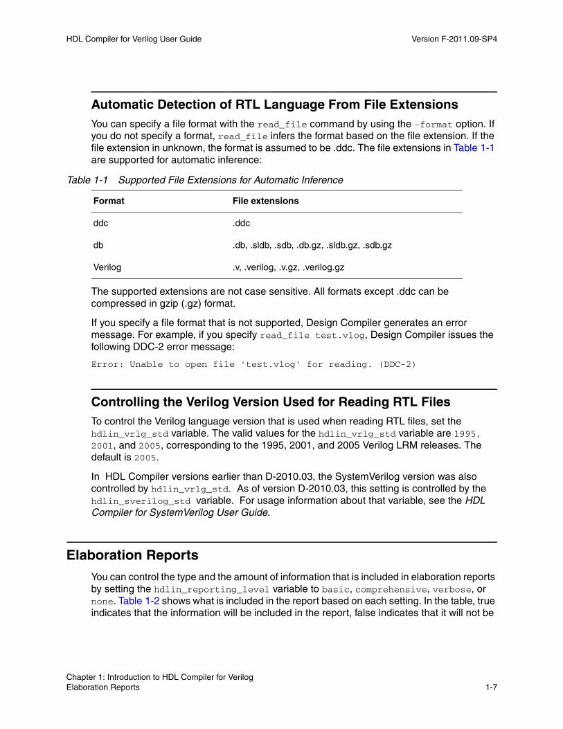
Automatic Detection of RTL Language From File ExtensionsYou can specify a file format with the read_file command by using the -format option. If you do not specify a format, read_file infers the format based on the file extension. If the file extension in unknown, the format is assumed to be .ddc. The file extensions in Table 1-1 are supported for automatic inference:
Table 1-1 Supported File Extensions for Automatic Inference
Format File extensions
ddc .ddc
db .db, .sldb, .sdb, .db.gz, .sldb.gz, .sdb.gz
Verilog .v, .verilog, .v.gz, .verilog.gz
The supported extensions are not case sensitive. All formats except .ddc can be compressed in gzip (.gz) format.
If you specify a file format that is not supported, Design Compiler generates an error message. For example, if you specify read_file test.vlog, Design Compiler issues the following DDC-2 error message:
Error: Unable to open file 'test.vlog' for reading. (DDC-2)
Controlling the Verilog Version Used for Reading RTL FilesTo control the Verilog language version that is used when reading RTL files, set the hdlin_vrlg_std variable. The valid values for the hdlin_vrlg_std variable are 1995, 2001, and 2005, corresponding to the 1995, 2001, and 2005 Verilog LRM releases. The default is 2005.
In HDL Compiler versions earlier than D-2010.03, the SystemVerilog version was also controlled by hdlin_vrlg_std. As of version D-2010.03, this setting is controlled by the hdlin_sverilog_std variable. For usage information about that variable, see the HDL Compiler for SystemVerilog User Guide.
Elaboration Reports
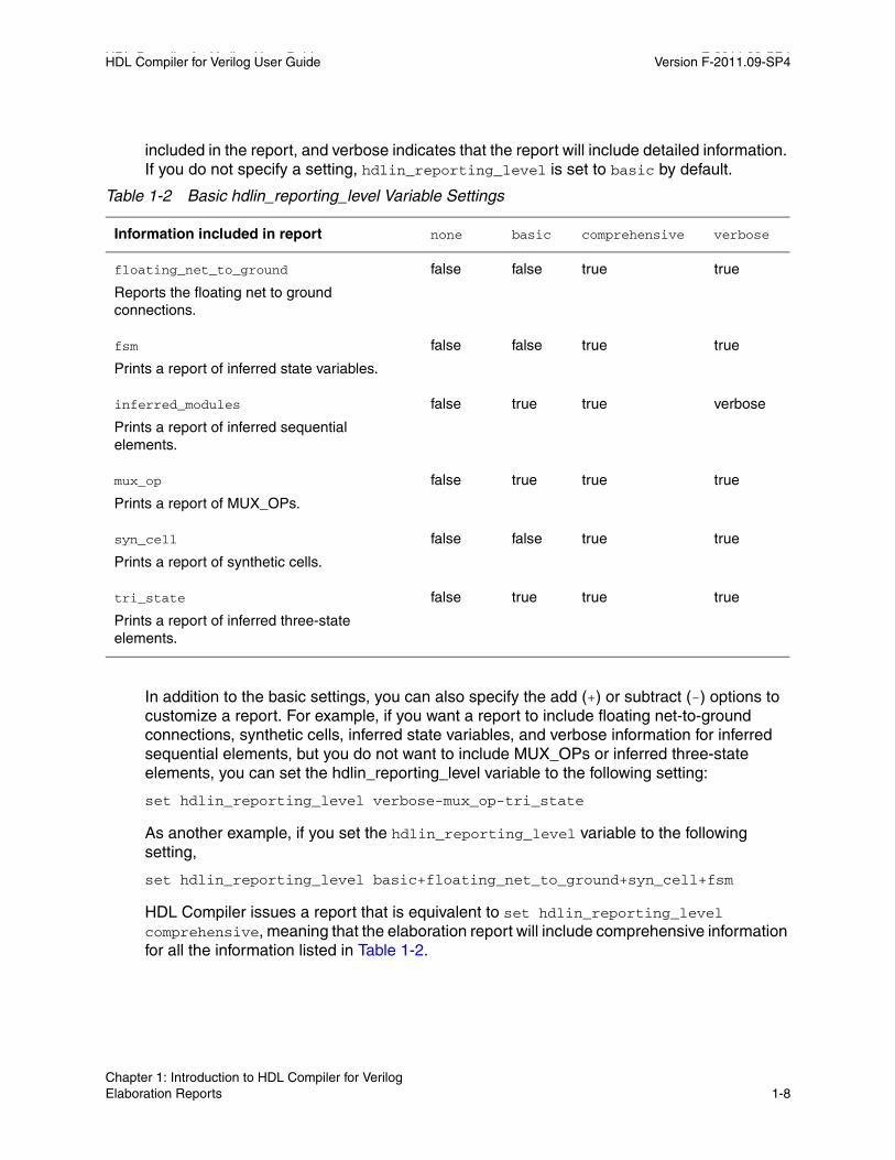
You can control the type and the amount of information that is included in elaboration reports by setting the hdlin_reporting_level variable to basic, comprehensive, verbose, or none. Table 1-2 shows what is included in the report based on each setting. In the table, true indicates that the information will be included in the report, false indicates that it will not be
Chapter 1: Introduction to HDL Compiler for Verilog Elaboration Reports 1-7Chapter 1: Introduction to HDL Compiler for Verilog Elaboration Reports 1-7
HDL Compiler for Verilog User Guide F-2011.09-SP4HDL Compiler for Verilog User Guide Version F-2011.09-SP4
included in the report, and verbose indicates that the report will include detailed information. If you do not specify a setting, hdlin_reporting_level is set to basic by default.
Table 1-2 Basic hdlin_reporting_level Variable Settings
Information included in report none basic comprehensive verbose
floating_net_to_ground
Reports the floating net to ground connections.
false false true true
fsm
Prints a report of inferred state variables.
false false true true
inferred_modules
Prints a report of inferred sequential elements.
false true true verbose
mux_op
Prints a report of MUX_OPs.
false true true true
syn_cell
Prints a report of synthetic cells.
false false true true
tri_state
Prints a report of inferred three-state elements.
false true true true
In addition to the basic settings, you can also specify the add (+) or subtract (-) options to customize a report. For example, if you want a report to include floating net-to-ground connections, synthetic cells, inferred state variables, and verbose information for inferred sequential elements, but you do not want to include MUX_OPs or inferred three-state elements, you can set the hdlin_reporting_level variable to the following setting:
set hdlin_reporting_level verbose-mux_op-tri_state
As another example, if you set the hdlin_reporting_level variable to the following setting,
set hdlin_reporting_level basic+floating_net_to_ground+syn_cell+fsm
HDL Compiler issues a report that is equivalent to set hdlin_reporting_level comprehensive, meaning that the elaboration report will include comprehensive information for all the information listed in Table 1-2.
Chapter 1: Introduction to HDL Compiler for Verilog Elaboration Reports 1-8

HDL Compiler for Verilog User Guide Version F-2011.09-SP4
Reporting Elaboration Errors
HDL Compiler elaborates designs in a top-down hierarchical order. The elaboration failure of a top-level module prohibits the elaboration of all associated submodules. The hdlin_elab_errors_deep variable allows the elaboration of submodules even if the top-level module elaboration fails, enabling HDL Compiler to report more elaboration, link, and VER-37 errors and warnings in a hierarchical design during the first elaboration run.
To understand how this variable works, consider the four-level hierarchical design in Figure 1-1. This design has elaboration (ELAB) errors as noted in the figure.
Figure 1-1 Hierarchical Design
TOP
B C
E
ELAB-360 ELAB-298ELAB-368 ELAB-298
A
ELAB-298
D
F
G
Level 1
Level 2
Level 3
Level 4
Under default conditions, when you elaborate the design, HDL Compiler only reports the errors in the first-level (ELAB-368 and ELAB-298 in module A). To find the second-level error (ELAB-298 in submodule D), you need to fix the first-level errors and elaborate again.
When you use the hdlin_elab_errors_deep variable, you only need to elaborate once to find the errors in A and the submodule D.
Chapter 1: Introduction to HDL Compiler for Verilog Reporting Elaboration Errors 1-9Chapter 1: Introduction to HDL Compiler for Verilog Reporting Elaboration Errors 1-9
HDL Compiler for Verilog User Guide F-2011.09-SP4HDL Compiler for Verilog User Guide Version F-2011.09-SP4
This section describes the hdlin_elab_errors_deep variable and provides methodology and examples:
• Methodology
• Examples
MethodologyUse the following methodology to enable HDL Compiler to report elaboration, link, and VER-37 errors across the hierarchy during a single elaboration run.
1. Identify and fix all syntax errors in the design.
2. Set hdlin_elab_errors_deep to true.
When you set this variable to true, HDL Compiler reports the following:
*** HDLC compilation run in rtl debug mode. ***
Important: HDL Compiler does not create designs when you set hdlin_elab_errors_deep to true. The tool reports warnings if you try to use commands that require a design. For example, if you run the list_designs command, the tool reports the message “Warning: No designs to list. (UID-275).”
3. Elaborate your design using the elaborate command.
4. Fix any elaboration, link, and VER-37 errors. Review the warnings and fix as needed.
5. Set hdlin_elab_errors_deep to false.
6. Elaborate your error-free design.
7. Proceed with your normal synthesis flow.
The next section provides examples showing HDL Compiler reporting all errors across the hierarchy, which reduces the need for multiple elaboration runs.
ExamplesTo enable HDL Compiler to report errors down the hierarchy in one elaboration run, you can set the hdlin_elab_errors_deep variable to true, changing it from its default of false. This variable is designed to speed up the time in finding design elaboration and linking errors.
Chapter 1: Introduction to HDL Compiler for Verilog Reporting Elaboration Errors 1-10

HDL Compiler for Verilog User Guide Version F-2011.09-SP4
This section uses the top design in Figure 1-2 as an example of reporting hierarchical errors. The error messages are shown in the figure. Example 1-1 lists the RTL code of the top design.
Figure 1-2 Hierarchical Design
top
sub2 LINK-3
sub3
ELAB-360 ELAB-298ELAB-368 ELAB-298
sub1
ELAB-298
mysub
bar
phi
sub2
Example 1-1 Verilog RTL for the top Design
module top (clk, a, b, c, out, small_bus); parameter SMALL = 8; input clk, a, b; output c, out; output [SMALL-1:0] small_bus; sub1 sub1_inst (clk, a, b, c, out, small_bus); sub2 sub2_inst (a, b, c); sub3 sub3_inst (a, b, c);endmodule
module sub1 (clk, a, b, c, out, small_bus); parameter SMALL = 8; input clk, a, b; output c, out;
Chapter 1: Introduction to HDL Compiler for Verilog Reporting Elaboration Errors 1-11Chapter 1: Introduction to HDL Compiler for Verilog Reporting Elaboration Errors 1-11
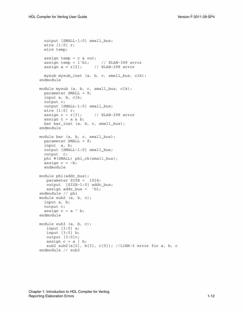
HDL Compiler for Verilog User Guide F-2011.09-SP4HDL Compiler for Verilog User Guide Version F-2011.09-SP4
output [SMALL-1:0] small_bus; wire [1:0] r; wire temp;
assign temp = c & out; assign temp = 1'b1; // ELAB-368 error assign a = r[2]; // ELAB-298 error mysub mysub_inst (a, b, c, small_bus, clk);endmodule
module mysub (a, b, c, small_bus, clk); parameter SMALL = 8; input a, b, clk; output c; output [SMALL-1:0] small_bus; wire [1:0] r; assign c = r[3]; // ELAB-298 error assign c = a & b; bar bar_inst (a, b, c, small_bus);endmodule
module bar (a, b, c, small_bus); parameter SMALL = 8; input a, b; output [SMALL-1:0] small_bus; output c; phi #(SMALL) phi_ok(small_bus); assign c = ~b; endmodule
module phi(addr_bus); parameter SIZE = 1024; output [SIZE-1:0] addr_bus; assign addr_bus = 'b1;endmodule // phimodule sub2 (a, b, c); input a, b; output c; assign c = a ^ b;endmodule
module sub3 (a, b, c); input [3:0] a; input [3:0] b; output [3:0]c; assign c = a | b; sub2 sub2(a[2], b[3], c[0]); //LINK-3 error for a, b, cendmodule // sub3
Chapter 1: Introduction to HDL Compiler for Verilog Reporting Elaboration Errors 1-12
HDL Compiler for Verilog User Guide Version F-2011.09-SP4
When you elaborate the top design with the hdlin_elab_errors_deep variable set to false, HDL Compiler reports the first-level errors, the ELAB-368 and ELAB-298 errors in the sub1 module and the LINK-3 error in the sub3 module, but it does not report the ELAB-298 error in the mysub submodule. Example 1-2 shows the session log.
Example 1-2 Session Log
Initializing...Initializing gui preferences from file /.../.synopsys_dv_prefs.tcldc_shell> analyze -f verilog test.vRunning HDLCSearching for ./test.vCompiling source file ./test.vWarning: ./test.v:22: Port a of type input is being assigned. (VER-1005)HDLC compilation completed successfully.Loading db file '/.../libraries/syn/lsi_10k.db'1dc_shell> elaborate topLoading db file '/.../libraries/syn/gtech.db'Loading db file '/.../libraries/syn/standard.sldb' Loading link library 'lsi_10k' Loading link library 'gtech'Running HDLCHDLC compilation completed successfully.Elaborated 1 design.Current design is now 'top'.Information: Building the design 'sub1'. (HDL-193)Error: ./test.v:21: Net 'temp', or a directly connected net, is driven by more than one source, and at least one source is a constant net. (ELAB-368)Error: ./test.v:22: Array index out of bounds r[2], valid bounds are [1:0]. (ELAB-298)*** HDLC compilation terminated with 2 errors. ***Information: Building the design 'sub2'. (HDL-193)HDLC compilation completed successfully.Information: Building the design 'sub3'. (HDL-193)HDLC compilation completed successfully.Error: Width mismatch on port 'a' of reference to 'sub3' in 'top'. (LINK-3)Error: Width mismatch on port 'b' of reference to 'sub3' in 'top'. (LINK-3)Error: Width mismatch on port 'c' of reference to 'sub3' in 'top'. (LINK-3)Warning: Design 'top' has '1' unresolved references. For more detailed information, use the "link" command. (UID-341)1dc_shell> current_design
Chapter 1: Introduction to HDL Compiler for Verilog Reporting Elaboration Errors 1-13Chapter 1: Introduction to HDL Compiler for Verilog Reporting Elaboration Errors 1-13

HDL Compiler for Verilog User Guide F-2011.09-SP4HDL Compiler for Verilog User Guide Version F-2011.09-SP4
Current design is 'top'.{top}dc_shell> list_designssub2 sub3 top (*)1
When you set the hdlin_elab_errors_deep variable to true, HDL Compiler reports errors down the hierarchy during elaboration. Example 1-3 shows the session log with all the error messages.
Example 1-3 Session Log With All the Error Messages
Initializing...Initializing gui preferences from file /.../.synopsys_dv_prefs.tcldc_shell> set hdlin_elab_errors_deep TRUETRUEdc_shell> analyze -f verilog test.vRunning HDLCSearching for ./test.vCompiling source file ./test.vWarning: ./test.v:22: Port a of type input is being assigned. (VER-1005)HDLC compilation completed successfully.Loading db file '/.../libraries/syn/lsi_10k.db'1dc_shell> elaborate topLoading db file '/.../libraries/syn/gtech.db'Loading db file '/.../libraries/syn/standard.sldb' Loading link library 'lsi_10k' Loading link library 'gtech'Running HDLC*** HDLC compilation run in rtl debug mode. ***HDLC compilation completed successfully.Elaborated 1 design.Current design is now 'top'.Information: Building the design 'sub1'. (HDL-193)*** HDLC compilation run in rtl debug mode. ***Error: ./test.v:21: Net 'temp', or a directly connected net, is driven by more than one source, and at least one source is a constant net. (ELAB-368)Error: ./test.v:22: Array index out of bounds r[2], valid bounds are [1:0]. (ELAB-298)*** HDLC compilation terminated with 2 errors. ***Information: Building the design 'sub2'. (HDL-193)*** HDLC compilation run in rtl debug mode. ***HDLC compilation completed successfully.Information: Building the design 'sub3'. (HDL-193)*** HDLC compilation run in rtl debug mode. ***HDLC compilation completed successfully.Error: Width mismatch on port 'a' of reference to 'sub3' in 'top'. (LINK-3)
Chapter 1: Introduction to HDL Compiler for Verilog Reporting Elaboration Errors 1-14
HDL Compiler for Verilog User Guide Version F-2011.09-SP4
Error: Width mismatch on port 'b' of reference to 'sub3' in 'top'. (LINK-3)Error: Width mismatch on port 'c' of reference to 'sub3' in 'top'. (LINK-3)Information: Building the design 'mysub'. (HDL-193)*** HDLC compilation run in rtl debug mode. ***Error: ./test.v:32: Array index out of bounds r[3], valid bounds are [1:0]. (ELAB-298)*** HDLC compilation terminated with 1 errors. ***Information: Building the design 'bar'. (HDL-193)*** HDLC compilation run in rtl debug mode. ***HDLC compilation completed successfully.Information: Building the design 'phi' instantiated from design 'bar' with the parameters "8". (HDL-193)*** HDLC compilation run in rtl debug mode. ***HDLC compilation completed successfully.1dc_shell> current_designError: Current design is not defined. (UID-4)dc_shell> list_designsWarning: No designs to list. (UID-275)0
By default, only the top-level errors are reported:
• ELAB-368 and ELAB-298 in the sub1 module
• LINK-3 in the sub3 module
To find the child-level ELAB-298 error in the mysub submodule, you need to fix all the errors in the sub1 and sub3 modules and run the elaborate command again. However, when you set the hdlin_elab_errors_deep variable to true, HDL Compiler reports all errors down the hierarchy in one elaboration run:
• ELAB-368 and ELAB-298 in the sub1 module
• LINK-3 in the sub3 module
• ELAB-298 in the mysub submodule
When the hdlin_elab_errors_deep variable is set to true, note the following guidelines:
• No designs are saved because the designs could be erroneous.
• The compile_ultra and list_designs commands do not work.
• You should use the analyze command rather than the read_file command to read your design because the read_file command has no link functionality and accepts no command-line parameter specifications.
Chapter 1: Introduction to HDL Compiler for Verilog Reporting Elaboration Errors 1-15Chapter 1: Introduction to HDL Compiler for Verilog Reporting Elaboration Errors 1-15

HDL Compiler for Verilog User Guide F-2011.09-SP4HDL Compiler for Verilog User Guide Version F-2011.09-SP4
• All syntax errors are reported when you run the analyze command, but HDL Compiler is not a linting tool. You should use the check_design command in Design Compiler for linting.
• The runtime during elaboration might increase slightly.
Important: HDL Compiler does not create designs when the hdlin_elab_errors_deep variable is set to true. If you run the list_designs command, HDL Compiler reports the following warning:
Warning: No designs to list. (UID-275)
Netlist Reader
Design Compiler contains a specialized reader for gate-level Verilog netlists that has higher capacity on designs that do not use RTL-level constructs, but it does not support the entire Verilog language. The specialized netlist reader reads netlists faster and uses less memory than HDL Compiler.
If you have problems reading a netlist with the netlist reader, try reading it with HDL Compiler by using read_verilog -rtl or by specifying read_file -format verilog -rtl.
Automatic Detection of Input Type
By default, when you read in a Verilog gate-level netlist, HDL Compiler determines that your design is a netlist and runs the specialized netlist reader.
Important: For best memory usage and runtime, do not mix RTL and netlist designs into a single read. The automatic detector chooses one reader—netlist or RTL—to read all files included in the command. Mixed files default to the RTL reader, because it can read both types; the netlist reader can read only netlists.
The following variables apply only to HDL Compiler and are not implemented by the netlist reader:
• power_preserve_rtl_hier_names (default is false)
• hdlin_auto_save_templates (default is false)
If you set either of these variables to true (the nondefault value), automatic netlist detection is disabled and you must use the -netlist option to enable the netlist reader.
Chapter 1: Introduction to HDL Compiler for Verilog Netlist Reader 1-16
HDL Compiler for Verilog User Guide Version F-2011.09-SP4
Reading In Designs
Table 1-3 summarizes the recommended and alternative commands to read in your designs.
Table 1-3 Reading Commands
Type of input Reading method
RTL For parameterized designs, analyze -format verilog { files } elaborate topdesign is preferred because it does a recursive elaboration of the entire design and lets you pass parameter values to the elaboration. The read method conditionally elaborates all designs with the default parameters. To enable macro definition from the read, use read_file -format verilog { files } Alternative reading methods: read_verilog -rtl { files } read_file -format verilog -rtl { files }
Gate-level netlists Recommended reading method: read_verilog { files } Alternative reading methods: read_verilog -netlist { files } read_file -format verilog -netlist { files }
Defining Macros
HDL Compiler provides the following support for macro definition.
Using analyze -defineYou can use analyze -define to define macros on the command line; see “`define” on page B-17 for more information.
Note: When using the -define option with multiple analyze commands, you must remove any designs in memory before re-analyzing the design. To remove the designs, use the remove_design -all command. Because elaborated designs in memory have no timestamps, the tool cannot determine whether the analyzed file has been updated. The tool may assume that the previously elaborated design is up-to-date and reuse it.
Chapter 1: Introduction to HDL Compiler for Verilog Reading In Designs 1-17Chapter 1: Introduction to HDL Compiler for Verilog Reading In Designs 1-17
HDL Compiler for Verilog User Guide F-2011.09-SP4HDL Compiler for Verilog User Guide Version F-2011.09-SP4
Predefined Macros You can also use the following predefined macros:
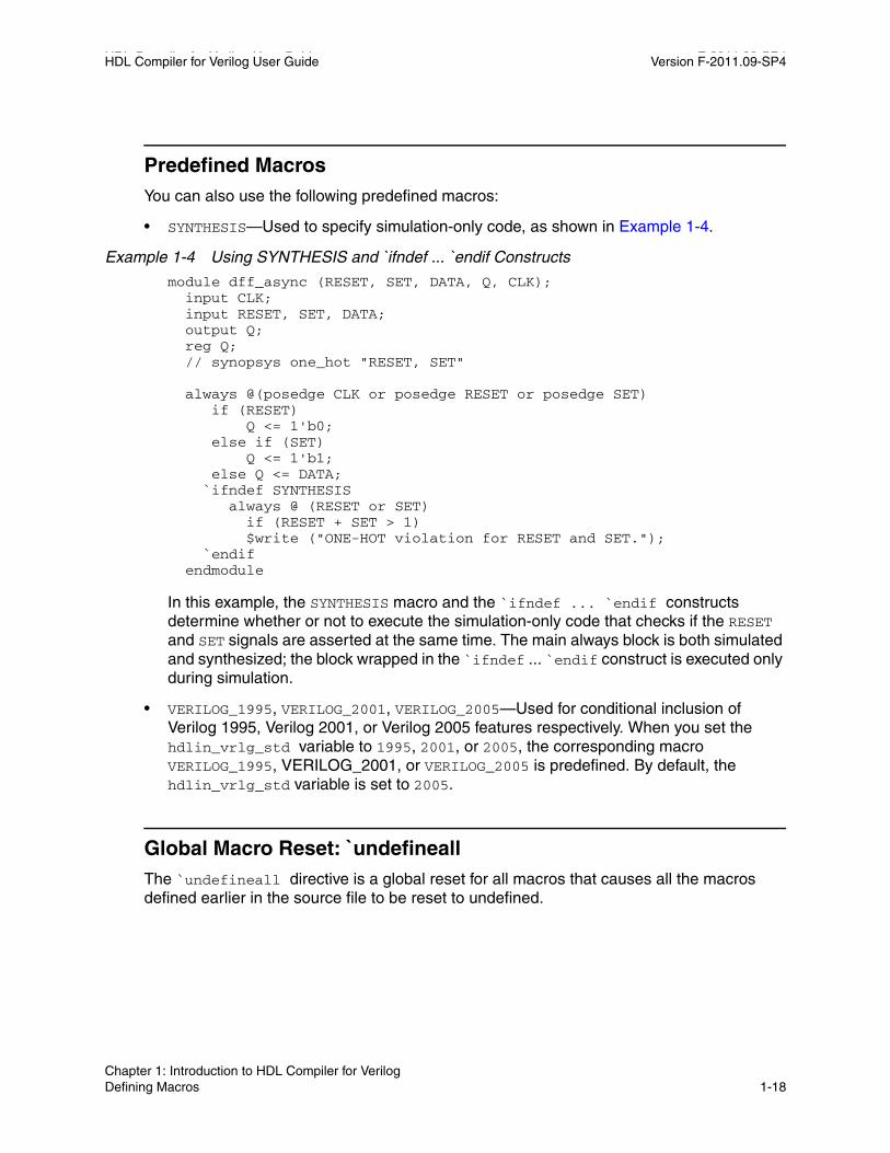
• SYNTHESIS—Used to specify simulation-only code, as shown in Example 1-4.
Example 1-4 Using SYNTHESIS and `ifndef ... `endif Constructs
module dff_async (RESET, SET, DATA, Q, CLK); input CLK; input RESET, SET, DATA; output Q; reg Q; // synopsys one_hot "RESET, SET"
always @(posedge CLK or posedge RESET or posedge SET) if (RESET) Q <= 1'b0; else if (SET) Q <= 1'b1; else Q <= DATA; `ifndef SYNTHESIS always @ (RESET or SET) if (RESET + SET > 1) $write ("ONE-HOT violation for RESET and SET."); `endif endmodule
In this example, the SYNTHESIS macro and the `ifndef ... `endif constructs determine whether or not to execute the simulation-only code that checks if the RESET and SET signals are asserted at the same time. The main always block is both simulated and synthesized; the block wrapped in the ̀ ifndef ... ̀ endif construct is executed only during simulation.
• VERILOG_1995, VERILOG_2001, VERILOG_2005—Used for conditional inclusion of Verilog 1995, Verilog 2001, or Verilog 2005 features respectively. When you set the hdlin_vrlg_std variable to 1995, 2001, or 2005, the corresponding macro VERILOG_1995, VERILOG_2001, or VERILOG_2005 is predefined. By default, the hdlin_vrlg_std variable is set to 2005.
Global Macro Reset: `undefineall The `undefineall directive is a global reset for all macros that causes all the macros defined earlier in the source file to be reset to undefined.
Chapter 1: Introduction to HDL Compiler for Verilog Defining Macros 1-18
HDL Compiler for Verilog User Guide Version F-2011.09-SP4
Parameterized Designs
There are two ways to build parameterized designs. One method instantiates them, as shown in Example 1-5.
Example 1-5 Instantiating a Parameterized Design
module param (a,b,c);
input [3:0] a,b;output [3:0] c;
foo #(4,5,4+6) U1(a,b,c); // instantiate foo
endmodule
In Example 1-5, the code instantiates the parameterized design foo, which has three parameters. The first parameter is assigned the value 4, the second parameter is assigned the value 5, and the third parameter takes the value 10.
The second method builds a parameterized design with the elaborate command. The syntax of the command is
elaborate template_name -parameters parameter_list
The syntax of the parameter specifications includes strings, integers, and constants using the following formats `b,`h, b, and h.
You can store parameterized designs in user-specified design libraries. For example,
analyze -format verilog n-register.v -library mylib
This command stores the analyzed results of the design contained in file n-register.v in a user-specified design library, mylib.
To verify that a design is stored in memory, use the report_design_lib work command. The report_design_lib command lists designs that reside in the indicated design library.
When a design is built from a template, only the parameters you indicate when you instantiate the parameterized design are used in the template name. For example, suppose the template ADD has parameters N, M, and Z. You can build a design where N = 8, M = 6, and Z is left at its default value. The name assigned to this design is ADD_N8_M6. If no parameters are listed, the template is built with default values, and the name of the created design is the same as the name of the template. If no default parameters are provided, an error occurs.
The model in Example 1-6 uses a parameter to determine the register bit-width; the default width is declared as 8.
Chapter 1: Introduction to HDL Compiler for Verilog Parameterized Designs 1-19Chapter 1: Introduction to HDL Compiler for Verilog Parameterized Designs 1-19
HDL Compiler for Verilog User Guide F-2011.09-SP4HDL Compiler for Verilog User Guide Version F-2011.09-SP4
Example 1-6 Register Model
module DFF ( in1, clk, out1 ); parameter SIZE = 8; input [SIZE-1:0] in1; input clk; output [SIZE-1:0] out1; reg [SIZE-1:0] out1; reg [SIZE-1:0] tmp;
always @(clk) if (clk == 0) tmp = in1; else //(clk == 1) out1 <= tmp;endmodule
If you want an instance of the register model to have a bit-width of 16, use the elaborate command to specify this as follows:
elaborate DFF -param SIZE=16
The list_designs command shows the design, as follows:
DFF_SIZE16 (*)
Using the read_verilog command to build a design with parameters is not recommended because you can build a design only with the default value of the parameters.
You also need to either set the hdlin_auto_save_templates variable to true or insert the template directive in the module, as follows:
module DFF ( in1, clk, out1 ); parameter SIZE = 8; input [SIZE-1:0] in1; input clk; output [SIZE-1:0] out1; // synopsys template...
The following three variables control the naming convention for templates: hdlin_template_naming_style, hdlin_template_parameter_style, and hdlin_template_separator_style. For details, see Chapter 8, “HDL Compiler Variables.
Reading Large Designs
To easily read designs containing several HDL source files and libraries, use the analyze command with the -vcs option. VCS-style analyze provides better compatibility with VCS command options and makes it easier to read in large designs. This feature enables
Chapter 1: Introduction to HDL Compiler for Verilog Reading Large Designs 1-20
HDL Compiler for Verilog User Guide Version F-2011.09-SP4
automatic resolution of instantiated designs by searching for the referenced designs in user-specified libraries and then loading these designs. Use the following options with -vcs:
[-sverilog|-verilog] [-y directory_path] [+libext+extension1+...] [-v library_file] [-f command_file] [+define+macro_name+...] [+incdir+directory_path+...]
For example, to read in a design containing Verilog modules and SystemVerilog modules and interfaces, execute the following commands:
analyze -vcs "-verilog -y mylibdir1 +libext+.v -v myfile1 +incdir+myincludedir1 -f mycmdfile2" top.vanalyze -vcs "-sverilog -y ./mylibdir2 +libext+.sv -v ./myfile2 +define+SYNOPSYS " top.sv
elaborate top
Limitations:
When using the analyze -vcs feature, you need to be aware of the following limitations:
1. Language elements other than modules, such as interfaces and structures, cannot be picked up from libraries or files using the -y and -v options.
2. A macro can be defined, but a value cannot be assigned to it. The value definition with +define is not supported.
These options follow the VCS command line syntax. For more details, see the VCS documentation and the analyze man page.
Use of $display During RTL Elaboration
The $display system task is usually used to report simulation progress. In synthesis, HDL Compiler executes $display calls as it sees them and executes all the display statements on all the paths through the program as it elaborates the design. It usually cannot tell the value of variables, except compile-time constants like loop iteration counters.
Note that because HDL Compiler executes all $display calls, error messages from the Verilog source can be executed and can look like unexpected messages.
Using $display is useful for printing out any compile-time computations on parameters or the number of times a loop executes. A $display example follows:
Chapter 1: Introduction to HDL Compiler for Verilog Use of $display During RTL Elaboration 1-21Chapter 1: Introduction to HDL Compiler for Verilog Use of $display During RTL Elaboration 1-21
HDL Compiler for Verilog User Guide F-2011.09-SP4HDL Compiler for Verilog User Guide Version F-2011.09-SP4
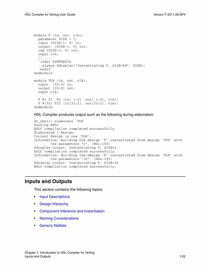
module F (in, out, clk); parameter SIZE = 1; input [SIZE-1: 0] in; output [SIZE-1: 0] out; reg [SIZE-1: 0] out; input clk; // ... `ifdef SYNTHESIS always $display("Instantiating F, SIZE=%d", SIZE); `endifendmodule
module TOP (in, out, clk); input [33:0] in; output [33:0] out; input clk;
F #( 2) F2 (in[ 1:0] ,out[ 1:0], clk); F #(32) F32 (in[33:2], out[33:2], clk);endmodule
HDL Compiler produces output such as the following during elaboration:
dc_shell> elaborate TOPRunning HDLCHDLC compilation completed successfully.Elaborated 1 design.Current design is now 'TOP'.Information: Building the design 'F' instantiated from design 'TOP' with the parameters "2". (HDL-193)$display output: Instantiating F, SIZE=2HDLC compilation completed successfully.Information: Building the design 'F' instantiated from design 'TOP' with the parameters "32". (HDL-193)$display output: Instantiating F, SIZE=32HDLC compilation completed successfully.
Inputs and Outputs
This section contains the following topics:
• Input Descriptions
• Design Hierarchy
• Component Inference and Instantiation
• Naming Considerations
• Generic Netlists
Chapter 1: Introduction to HDL Compiler for Verilog Inputs and Outputs 1-22

HDL Compiler for Verilog User Guide Version F-2011.09-SP4
• Inference Reports
• Error Messages
Input DescriptionsVerilog code input to HDL Compiler can contain both structural and functional (RTL) descriptions. A Verilog structural description can define a range of hierarchical and gate-level constructs, including module definitions, module instantiations, and netlist connections.
The functional elements of a Verilog description for synthesis include
• always statements
• Tasks and functions
• Assignments
❍ Continuous—are outside always blocks
❍ Procedural—are inside always blocks and can be either blocking or nonblocking
• Sequential blocks (statements between a begin and an end)
• Control statements
• Loops—for, while, forever
The forever loop is only supported if it has an associated disable condition, making the exit condition deterministic.
• case and if statements
Functional and structural descriptions can be used in the same module, as shown in Example 1-7.
In this example, the detect_logic function determines whether the input bit is a 0 or a 1. After making this determination, detect_logic sets ns to the next state of the machine. An always block infers flip-flops to hold the state information between clock cycles. These statements use a functional description style. A structural description style is used to instantiate the three-state buffer t1.
Chapter 1: Introduction to HDL Compiler for Verilog Inputs and Outputs 1-23Chapter 1: Introduction to HDL Compiler for Verilog Inputs and Outputs 1-23

HDL Compiler for Verilog User Guide F-2011.09-SP4HDL Compiler for Verilog User Guide Version F-2011.09-SP4
Example 1-7 Mixed Structural and Functional Descriptions// This finite state machine (Mealy type) reads one// bit per clock cycle and detects three or more// consecutive 1s.
module three_ones( signal, clock, detect, output_enable );input signal, clock, output_enable;output detect;// Declare current state and next state variables.reg [1:0] cs;reg [1:0] ns;wire ungated_detect;// Declare the symbolic names for states.parameter NO_ONES = 0, ONE_ONE = 1,
TWO_ONES = 2, AT_LEAST_THREE_ONES = 3;// ************* STRUCTURAL DESCRIPTION ****************// Instance of a three-state gate that enables outputthree_state t1 (ungated_detect, output_enable, detect);
// ************* FUNCTIONAL DESCRIPTION ****************// always block infers flip-flops to hold the state of // the FSM.always @ ( posedge clock ) begin
cs = ns;end// Combinational functionfunction detect_logic;
input [1:0] cs; input signal;
begindetect_logic = 0; //default valueif ( signal == 0 ) //bit is zero
ns = NO_ONES;else //bit is one, increment statecase (cs)
NO_ONES: ns = ONE_ONE;ONE_ONE: ns = TWO_ONES;TWO_ONES, AT_LEAST_THREE_ONES:
beginns = AT_LEAST_THREE_ONES;detect_logic = 1;end
endcaseend
endfunctionassign ungated_detect = detect_logic( cs, signal );
endmodule
Chapter 1: Introduction to HDL Compiler for Verilog Inputs and Outputs 1-24

HDL Compiler for Verilog User Guide Version F-2011.09-SP4
Design HierarchyHDL Compiler maintains the hierarchical boundaries you define when you use structural Verilog. These boundaries have two major effects:
• Each module specified in your HDL description is synthesized separately and maintained as a distinct design. The constraints for the design are maintained, and each module can be optimized separately in Design Compiler.
• Module instantiations within HDL descriptions are maintained during input. The instance name you assign to user-defined components is carried through to the gate-level implementation.
Note: HDL Compiler does not automatically create the hierarchy for other, nonstructural Verilog constructs such as blocks, loops, functions, and tasks. These elements of an HDL description are translated in the context of their design. After reading in a Verilog design, you can use the group -hdl_block command to group the gates in a block, function, or task. HDL Compiler supports only the top-level always block. For information on how to use the group command with Verilog designs, see the man page.
Component Inference and InstantiationThere are two ways to define components in your Verilog description:
• You can directly instantiate registers into a Verilog description, selecting from any element in your ASIC library, but the code is technology dependent and the description is difficult to write.
• You can use Verilog constructs to direct HDL Compiler to infer registers from the description. The advantages are these:
❍ The Verilog description is easier to write and the code is technology independent.
❍ This method allows Design Compiler to select the type of component inferred, based on constraints.
If a specific component is necessary, use instantiation.
Naming ConsiderationsThe bus output instance names are controlled by the following variables: bus_naming_style (controls names of elements of Verilog arrays) and bus_inference_style (controls bus inference style). To reduce naming conflicts, use caution when applying nondefault naming styles. For details, see the man pages.
Chapter 1: Introduction to HDL Compiler for Verilog Inputs and Outputs 1-25Chapter 1: Introduction to HDL Compiler for Verilog Inputs and Outputs 1-25

HDL Compiler for Verilog User Guide F-2011.09-SP4HDL Compiler for Verilog User Guide Version F-2011.09-SP4
Generic Netlists After HDL Compiler reads a design, it creates a generic netlist consisting of generic components, such as SEQGENs (see “Generic Sequential Cells (SEQGENs)” on page 4-2.)
For example, after HDL Compiler reads the my_fsm design in Example 1-8 on page 1-26, it creates the generic netlist shown in Example 1-9 on page 1-27.
Example 1-8
module my_fsm (clk, rst, y); input clk, rst; output y; reg y; reg [2:0] current_state; parameter red = 3'b001, green = 3'b010, yellow = 3'b100; always @ (posedge clk or posedge rst) if (rst) current_state = red; else case (current_state) red: current_state = green; green: current_state = yellow; yellow: current_state = red; default: current_state = red; endcase always @ (current_state) if (current_state == yellow) y = 1'b1; else y = 1'b0; endmodule
After HDL Compiler reads in the my_fsm design, it outputs the generic netlist shown in Example 1-9.
Chapter 1: Introduction to HDL Compiler for Verilog Inputs and Outputs 1-26
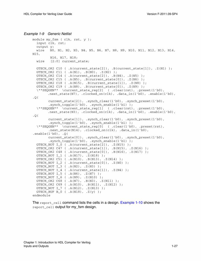
HDL Compiler for Verilog User Guide Version F-2011.09-SP4
Example 1-9 Generic Netlist
module my_fsm ( clk, rst, y ); input clk, rst; output y; wire N0, N1, N2, N3, N4, N5, N6, N7, N8, N9, N10, N11, N12, N13, N14, N15, N16, N17, N18; wire [2:0] current_state;
GTECH_OR2 C10 ( .A(current_state[2]), .B(current_state[1]), .Z(N1) ); GTECH_OR2 C11 ( .A(N1), .B(N0), .Z(N2) ); GTECH_OR2 C14 ( .A(current_state[2]), .B(N4), .Z(N5) ); GTECH_OR2 C15 ( .A(N5), .B(current_state[0]), .Z(N6) ); GTECH_OR2 C18 ( .A(N15), .B(current_state[1]), .Z(N8) ); GTECH_OR2 C19 ( .A(N8), .B(current_state[0]), .Z(N9) ); \**SEQGEN** \current_state_reg[2] ( .clear(rst), .preset(1'b0), .next_state(N7), .clocked_on(clk), .data_in(1'b0), .enable(1'b0), .Q( current_state[2]), .synch_clear(1'b0), .synch_preset(1'b0), .synch_toggle(1'b0), .synch_enable(1'b1) ); \**SEQGEN** \current_state_reg[1] ( .clear(rst), .preset(1'b0), .next_state(N3), .clocked_on(clk), .data_in(1'b0), .enable(1'b0), .Q( current_state[1]), .synch_clear(1'b0), .synch_preset(1'b0), .synch_toggle(1'b0), .synch_enable(1'b1) ); \**SEQGEN** \current_state_reg[0] ( .clear(1'b0), .preset(rst), .next_state(N14), .clocked_on(clk), .data_in(1'b0), .enable(1'b0), .Q( current_state[0]), .synch_clear(1'b0), .synch_preset(1'b0), .synch_toggle(1'b0), .synch_enable(1'b1) ); GTECH_NOT I_0 ( .A(current_state[2]), .Z(N15) ); GTECH_OR2 C47 ( .A(current_state[1]), .B(N15), .Z(N16) ); GTECH_OR2 C48 ( .A(current_state[0]), .B(N16), .Z(N17) ); GTECH_NOT I_1 ( .A(N17), .Z(N18) ); GTECH_OR2 C51 ( .A(N10), .B(N13), .Z(N14) ); GTECH_NOT I_2 ( .A(current_state[0]), .Z(N0) ); GTECH_NOT I_3 ( .A(N2), .Z(N3) ); GTECH_NOT I_4 ( .A(current_state[1]), .Z(N4) ); GTECH_NOT I_5 ( .A(N6), .Z(N7) ); GTECH_NOT I_6 ( .A(N9), .Z(N10) ); GTECH_OR2 C68 ( .A(N7), .B(N3), .Z(N11) ); GTECH_OR2 C69 ( .A(N10), .B(N11), .Z(N12) ); GTECH_NOT I_7 ( .A(N12), .Z(N13) ); GTECH_BUF B_0 ( .A(N18), .Z(y) );endmodule
The report_cell command lists the cells in a design. Example 1-10 shows the report_cell output for my_fsm design.
Chapter 1: Introduction to HDL Compiler for Verilog Inputs and Outputs 1-27Chapter 1: Introduction to HDL Compiler for Verilog Inputs and Outputs 1-27

HDL Compiler for Verilog User Guide F-2011.09-SP4HDL Compiler for Verilog User Guide Version F-2011.09-SP4
Example 1-10
dc_shell> report_cell Information: Updating design information... (UID-85) ****************************************Report : cellDesign : my_fsmVersion: B-2008.09Date : Tue Jul 15 07:11:02 2008****************************************
Attributes: b - black box (unknown) c - control logic h - hierarchical n - noncombinational r - removable u - contains unmapped logic
Cell Reference Library Area Attributes--------------------------------------------------------------------------------B_0 GTECH_BUF gtech 0.000000 uC10 GTECH_OR2 gtech 0.000000 uC11 GTECH_OR2 gtech 0.000000 c, uC14 GTECH_OR2 gtech 0.000000 uC15 GTECH_OR2 gtech 0.000000 c, uC18 GTECH_OR2 gtech 0.000000 uC19 GTECH_OR2 gtech 0.000000 c, uC47 GTECH_OR2 gtech 0.000000 uC48 GTECH_OR2 gtech 0.000000 uC51 GTECH_OR2 gtech 0.000000 uC68 GTECH_OR2 gtech 0.000000 c, uC69 GTECH_OR2 gtech 0.000000 c, uI_0 GTECH_NOT gtech 0.000000 uI_1 GTECH_NOT gtech 0.000000 uI_2 GTECH_NOT gtech 0.000000 uI_3 GTECH_NOT gtech 0.000000 uI_4 GTECH_NOT gtech 0.000000 uI_5 GTECH_NOT gtech 0.000000 uI_6 GTECH_NOT gtech 0.000000 uI_7 GTECH_NOT gtech 0.000000 c, ucurrent_state_reg[0] **SEQGEN** 0.000000 n, ucurrent_state_reg[1] **SEQGEN** 0.000000 n, ucurrent_state_reg[2] **SEQGEN** 0.000000 n, u-------------------------------------------------------------------------Total 23 cells 0.0000001
Chapter 1: Introduction to HDL Compiler for Verilog Inputs and Outputs 1-28
HDL Compiler for Verilog User Guide Version F-2011.09-SP4
Inference ReportsHDL Compiler generates inference reports for the following inferred components:
• Flip-flops and latches, described in “Inference Reports for Registers” on page 4-5.
• MUX_OP cells, described in “MUX_OP Inference” on page 3-15.
• Three-state devices, described in “Three-State Driver Inference Report” on page 6-2.
• Multibit devices, described in “infer_multibit and dont_infer_multibit” on page 7-9.
• FSMs, described in “FSM Inference Report” on page 5-5.
Error MessagesIf the design contains syntax errors, these are typically reported as ver-type errors; mapping errors, which occur when the design is translated to the target technology, are reported as elab-type errors. An error will cause the script you are currently running to terminate; a fatal error will terminate your Design Compiler session. Warnings are errors that do not stop the read from completing, but the results might not be as expected.
The suppress_errors variable allows you to suppress warning messages when reading Verilog source files. If this variable is set to true, warnings are not issued; if false, warnings are issued. The default is false. This variable has no effect on fatal error messages, such as syntax errors, that stop the reading process.
You can also use this variable to disable specific warnings: set suppress_errors to a space-separated string of the error ID codes you want suppressed. Error ID codes are printed immediately after warning and error messages. For example, to suppress the warning
Warning: Assertion statements are not supported. They are ignored near symbol "assert" on line 24 (HDL-193).
set the variable to
suppress_errors = "HDL-193"
Language Construct Support
HDL Compiler supports only those constructs that can be synthesized, that is, realized in logic. For example, you cannot use simulation time as a trigger, because time is an element of the simulation process and cannot be realized in logic. See Appendix B, “Verilog Language Support.”
Chapter 1: Introduction to HDL Compiler for Verilog Language Construct Support 1-29Chapter 1: Introduction to HDL Compiler for Verilog Language Construct Support 1-29

HDL Compiler for Verilog User Guide F-2011.09-SP4HDL Compiler for Verilog User Guide Version F-2011.09-SP4
Licenses
Reading and writing license requirements are listed in Table 1-4.
Table 1-4 License Requirements
Reader
Reading license required
Writing license required
RTL Netlist RTL Netlist
HDL Compiler Yes Yes No No
UNTI-Verilog (netlist reader)
Not applicable
No Not applicable No
Automatic detection (read_verilog)
Yes Yes Not applicable Not applicable
Chapter 1: Introduction to HDL Compiler for Verilog Licenses 1-30

2Coding Considerations 2
This chapter describes HDL Compiler synthesis coding considerations in the following sections:
• Coding for QoR
• Creating Relative Placement in Hardware Description Languages
• General Coding Guidelines
• Interacting With Other Flows
2-1
HDL Compiler for Verilog User Guide F-2011.09-SP4HDL Compiler for Verilog User Guide Version F-2011.09-SP4
Coding for QoR
The goal of HDL Compiler is to provide the best QoR independent of coding style. However, the tool is limited to implementing your design based on the information (context) available at the time. You can use the following strategy to help ensure the tool has enough information to make good optimization decisions. HDL Compiler cannot determine if a module input is a constant even if the upper-level module connects it to a constant value. To expose it as a constant, use a parameter instead of an input port for that value.
Constant propagation is the compile-time evaluation of expressions that contain constants. HDL Compiler uses constant propagation to reduce the amount of hardware required to implement complex operators. When you know that a variable is a constant, specify it as a constant. For example, a + operator with a constant of 1 as one of its arguments causes an incrementer, rather than a general adder, to be built. If both arguments of an operator are constants, no hardware is constructed, because HDL Compiler can calculate the expression’s value and insert it directly into the circuit.
Comparators and shifters also benefit from constant propagation. When you shift a vector by a constant, the implementation requires only a reordering (rewiring) of bits, so no logic is needed.
Creating Relative Placement in Hardware Description Languages
Relative placement technology allows you to create structures in which you specify the relative column and row positions of instances. During placement and optimization, these structures are preserved and the cells in each structure are placed as a single entity.
Relative placement is usually applied to datapaths and registers, but you can apply it to any cells in your design, controlling the exact relative placement topology of gate-level logic groups and defining the circuit layout. You can use the relative placement capability to explore QoR benefits, such as shorter wire lengths, reduced congestion, better timing, skew control, fewer vias, better yield, and lower dynamic and leakage power.
The following sections describe restrictions, and how to specify relative placement data for RTL designs, GTECH netlists, or mapped netlists.
Relative placement constraints can also be added inside the shell using Tcl commands. For more information, see the “Using Design Compiler Topographical Technology” chapter in the Design Compiler User Guide.
Chapter 2: Coding Considerations Coding for QoR 2-2

HDL Compiler for Verilog User Guide Version F-2011.09-SP4
Support for Relative Placement Some restrictions apply when you specify relative placement.
The general restriction is that RTL and netlist relative placement directives cannot be mixed in the same file.
Other restrictions vary depending on whether you are using relative placement in an RTL design or an HDL netlist (a GTECH-level netlist or a mapped netlist).
For RTL designs, the following restrictions apply:
• You can specify relative placement directives only on register banks.
• When specifying relative placement for leaf-level registers, you must specify the relative placement directives inside an always block that infers registers and does not infer combinational logic.
If the always block does not infer registers, HDL Compiler generates the following error message:
Error: filename:line number: Relative placement register bank group 'rp group name does not contain a latch/FlipFlop. (ELAB-2)
These RTL restrictions do not apply to HDL netlists. For HDL netlists, the following conditions apply:
• You must use the HDL Compiler netlist reader to read in HDL netlists.
• In a GTECH-level netlist, you can apply relative placement directives only to cells that have a one-to-one mapping with library cells.
Examples of cells to which relative placement directives can normally be applied are AND gates, OR gates, and D flip-flops. Examples of cells to which they cannot be applied are SEQGENs (see “Generic Sequential Cells (SEQGENs)” on page 4-2), SELECT_OPs (see “SELECT_OP Inference” on page 3-13), MUX_OPs (see “MUX_OP Inference” on page 3-15), and DesignWare components (see “Synthetic Operators” on page 3-2).
• In mapped netlists, you can apply relative placement directives to any cell.
Chapter 2: Coding Considerations Creating Relative Placement in Hardware Description Languages 2-3Chapter 2: Coding Considerations Creating Relative Placement in Hardware Description Languages 2-3

HDL Compiler for Verilog User Guide F-2011.09-SP4HDL Compiler for Verilog User Guide Version F-2011.09-SP4
Directives for Specifying Relative PlacementYou can specify relative placement information by using the following HDL compiler directives:
• `rp_group and `rp_endgroup
See “Creating Groups Using `rp_group and `rp_endgroup” on page 2-4.
• `rp_place
See “Specifying Subgroups, Keepouts, and Instances Using `rp_place” on page 2-5.
• `rp_fill
See “Placing Cells Automatically Using `rp_fill” on page 2-6.
• `rp_array_dir
See “Specifying Placement for Array Elements Using `rp_array_dir” on page 2-8.
• rp_align
See “Specifying Cell Alignment Using rp_align” on page 2-8.
• rp_orient
See “Specifying Cell Orientation Using rp_orient” on page 2-9.
• rp_ignore and rp_endignore
See “Ignoring Relative Placement Using rp_ignore and rp_endignore” on page 2-10.
Note: For examples that show relative placement directives in RTL code, see “Relative Placement Examples” on page 2-10.
Creating Groups Using `rp_group and `rp_endgroupThe `rp_group and `rp_endgroup directives allow you to specify a relative placement group. The directives are available for RTL designs and netlist designs. For netlist designs, you must place all cell instances between the directives to declare them as members of the specified group. For RTL designs, you must specify the directives inside the always block for leaf-level relative placement groups. However, higher-level hierarchical groups do not have to be attached to an always block.
The Verilog syntax for RTL designs is as follows:
`rp_group ( group_name {num_cols num_rows} )`rp_endgroup ( {group_name} )
Chapter 2: Coding Considerations Creating Relative Placement in Hardware Description Languages 2-4
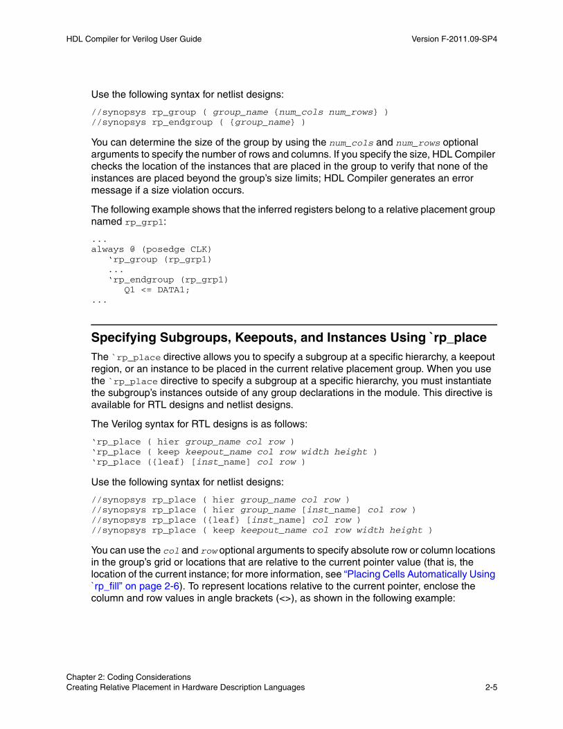
HDL Compiler for Verilog User Guide Version F-2011.09-SP4
Use the following syntax for netlist designs:
//synopsys rp_group ( group_name {num_cols num_rows} )//synopsys rp_endgroup ( {group_name} )
You can determine the size of the group by using the num_cols and num_rows optional arguments to specify the number of rows and columns. If you specify the size, HDL Compiler checks the location of the instances that are placed in the group to verify that none of the instances are placed beyond the group’s size limits; HDL Compiler generates an error message if a size violation occurs.
The following example shows that the inferred registers belong to a relative placement group named rp_grp1:
...always @ (posedge CLK) ‘rp_group (rp_grp1) ... ‘rp_endgroup (rp_grp1) Q1 <= DATA1;...
Specifying Subgroups, Keepouts, and Instances Using `rp_placeThe `rp_place directive allows you to specify a subgroup at a specific hierarchy, a keepout region, or an instance to be placed in the current relative placement group. When you use the `rp_place directive to specify a subgroup at a specific hierarchy, you must instantiate the subgroup’s instances outside of any group declarations in the module. This directive is available for RTL designs and netlist designs.
The Verilog syntax for RTL designs is as follows:
‘rp_place ( hier group_name col row )‘rp_place ( keep keepout_name col row width height )‘rp_place ({leaf} [inst_name] col row )
Use the following syntax for netlist designs:
//synopsys rp_place ( hier group_name col row )//synopsys rp_place ( hier group_name [inst_name] col row )//synopsys rp_place ({leaf} [inst_name] col row )//synopsys rp_place ( keep keepout_name col row width height )
You can use the col and row optional arguments to specify absolute row or column locations in the group’s grid or locations that are relative to the current pointer value (that is, the location of the current instance; for more information, see “Placing Cells Automatically Using `rp_fill” on page 2-6). To represent locations relative to the current pointer, enclose the column and row values in angle brackets (<>), as shown in the following example:
Chapter 2: Coding Considerations Creating Relative Placement in Hardware Description Languages 2-5Chapter 2: Coding Considerations Creating Relative Placement in Hardware Description Languages 2-5
HDL Compiler for Verilog User Guide F-2011.09-SP4HDL Compiler for Verilog User Guide Version F-2011.09-SP4
`rp_place (my_group_2 0 0)`rp_place (my_group_2 0 <1>)
The example shows that group my_group_1 is placed at location (0,0) in the grid, and group my_group_2 is placed at the next row position (0,1).
If you do not specify the col and row arguments, objects are automatically placed in the current group’s grid, filling empty slots. Each time a new instance is declared that is not explicitly placed, it is inserted into the grid at the location indicated by the current value of the pointer. After the instance is placed, the pointer is updated and the process is ready to be repeated.
The following Verilog example shows a relative placement group named my_reg_bank that includes four subgroups that are placed at the following locations, respectively: (0,0), (0,1), (1, *), and (1, *) The wildcard character (*) indicates that HDL Compiler can choose any value.
`rp_group (my_reg_bank)`rp_place (hier rp_grp1 0 0)`rp_place (hier rp_grp4 0 1)`rp_place (hier rp_grp2 1 *)`rp_place (hier rp_grp3 1 *)`rp_endgroup (my_reg_bank)
Placing Cells Automatically Using `rp_fillThe `rp_fill directive automatically places the cells at the location specified by a pointer. You can think of this as an imaginary pointer that specifies where the current cell should be placed. Unless you explicitly set it, the pointer initially points to 0,0 (column zero, row zero) and the first cell is placed at that location. Each time a new instance is declared that is not explicitly placed, it is inserted into the grid at the location indicated by the current value of the pointer. After the instance is placed, the pointer is updated incrementally and the process is ready to be repeated. This directive is available for RTL designs and netlist designs.
The Verilog syntax for RTL designs is as follows:
‘rp_fill ( {col row} {pattern pat} )
Use the following syntax for netlist designs:
//synopsys rp_fill ( col row} {pattern pat} )
The `rp_fill arguments define how the pointer is updated. The col and row parameters specify the initial coordinates of the pointer. These parameters can represent absolute row or column locations in the group’s grid or locations that are relative to the current pointer value. To represent locations relative to the current pointer, enclose the column and row values in angle brackets (<>); for absolute coordinates, use no brackets. For example,
Chapter 2: Coding Considerations Creating Relative Placement in Hardware Description Languages 2-6
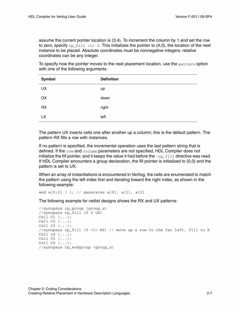
HDL Compiler for Verilog User Guide Version F-2011.09-SP4
assume the current pointer location is (3,4). To increment the column by 1 and set the row to zero, specify rp_fill <1> 0. This initializes the pointer to (4,0), the location of the next instance to be placed. Absolute coordinates must be nonnegative integers; relative coordinates can be any integer.
To specify how the pointer moves to the next placement location, use the pattern option with one of the following arguments:
Symbol Definition
UX up
DX down
RX right
LX left
The pattern UX inserts cells one after another up a column; this is the default pattern. The pattern RX fills a row with instances.
If no pattern is specified, the incremental operation uses the last pattern string that is defined. If the row and column parameters are not specified, HDL Compiler does not initialize the fill pointer, and it keeps the value it had before the ‘rp_fill directive was read. If HDL Compiler encounters a group declaration, the fill pointer is initialized to (0,0) and the pattern is set to UX.
When an array of instantiations is encountered in Verilog, the cells are enumerated to match the pattern using the left index first and iterating toward the right index, as shown in the following example:
and a[0:2] ( ); // generates a[0], a[1], a[2]
The following example for netlist designs shows the RX and UX patterns:
//synopsys rp_group (group_x) //synopsys rp_fill (0 0 UX) Cell C1 (...); Cell C2 (...); Cell C3 (...); //synopsys rp_fill (0 <1> RX) // move up a row to the far left, fill to R Cell c4 (...); Cell C5 (...); Cell C6 (...); //synopsys rp_endgroup (group_x)
Chapter 2: Coding Considerations Creating Relative Placement in Hardware Description Languages 2-7Chapter 2: Coding Considerations Creating Relative Placement in Hardware Description Languages 2-7
HDL Compiler for Verilog User Guide F-2011.09-SP4HDL Compiler for Verilog User Guide Version F-2011.09-SP4
Specifying Placement for Array Elements Using `rp_array_dirThe `rp_array_dir directive specifies whether the elements of an array are placed upward, from the least significant bit to the most significant bit, or downward, from the most significant bit to the least significant bit.
The Verilog syntax for RTL designs is as follows:
`rp_array_dir ( up|down )
The following Verilog example shows array elements that are placed upward, from the least significant bit to the most significant bit:
...always @ (posedge CLK) ‘rp_group (rp_grp1/ ‘rp_fill (0 0 UX) ‘rp_array_dir (up) ‘rp_endgroup (rp_grp1) Q1 <= DATA1 ;...
Note: This directive is available for creating relative placement in RTL designs but not in netlist designs.
Specifying Cell Alignment Using rp_alignNote:
This directive is available for creating relative placement in netlist designs only.
The rp_align directive explicitly specifies the alignment of the placed instance within the grid cell when the instance is smaller than the cell. If you specify the optional inst instance name argument, the alignment applies only to that instance; however, if you do not specify an instance, the new alignment applies to all subsequent instantiations within the group until HDL Compiler encounters another rp_align directive. If the instance straddles cells, the alignment takes place within the straddled region. The alignment value is sw (southwest) by default. The instance is snapped to legal row and routing grid coordinates.
Use the following syntax for netlist designs:
//synopsys rp_align ( n|s|e|w|nw|sw|ne|se|pin=name { inst })
You must specify either the alignment value or the pin name. In the following example, the rp_align directive causes the cell C1 to be placed at the north-east corner.
//synopsys rp_group (group_x)//synopsys rp_fill ( 0 0 RX )//synopsys rp_align (NE C1 )
Chapter 2: Coding Considerations Creating Relative Placement in Hardware Description Languages 2-8
HDL Compiler for Verilog User Guide Version F-2011.09-SP4
Cell C1 ...Cell C2 ...Cell C3 ...//synopsys rp_fill ( 0 <1> RX )Cell C4 ...Cell C5 ...Cell C6 ...//synopsys rp_endgroup (group_x)
Specifying Cell Orientation Using rp_orientNote:
This directive is available for creating relative placement in netlist designs only.
The rp_orient directive allows you to control the orientation of library cells placed in the current group. When you specify a list of possible orientations, HDL Compiler chooses the first legal orientation for the cell.
Use the following syntax for netlist designs:
//synopsys rp_orient ( {N|W|S|E|FN|FW|FS|FE}* { inst } )//synopsys rp_orient ( {N|W|S|E|FN|FW|FS|FE}* { group_name inst } ))
If you specify an instance value using the inst argument shown in the first (nonhierarchical) syntax format, the orientation applies only to that instance. If you do not specify an instance, the orientation applies to all subsequent instances until another orientation is specified.
If you specify the group_name inst syntax format, HDL Compiler applies the orientation to the specified instance, and the rest of the group remains unchanged. The default orientation for a group declaration is N, which stands for noflip nomirror, where flip refers to a rotation at the horizontal axis and mirror is a rotation at the vertical axis. The F value stands for flip; therefore, FN, FW, FS, and FE refer to flip north, flip west, flip south, and flip east, respectively.
In the following example, cell C1 is oriented westwards:
//synopsys rp_group (group_x)...//synopsys rp_orient (W C1) Cell C0 ...Cell C1 ......
Chapter 2: Coding Considerations Creating Relative Placement in Hardware Description Languages 2-9Chapter 2: Coding Considerations Creating Relative Placement in Hardware Description Languages 2-9
HDL Compiler for Verilog User Guide F-2011.09-SP4HDL Compiler for Verilog User Guide Version F-2011.09-SP4
Ignoring Relative Placement Using rp_ignore and rp_endignoreNote:
This directive is available for creating relative placement in netlist designs only.
The rp_ignore and rp_endignore directives allow you to ignore specified lines in the input file. Any lines between the two directives are omitted from relative placement. The include and define directives, variable substitution, and cell mapping are not ignored.
The rp_ignore and rp_endignore directives allow you to include the instantiation of submodules in a relative placement group close to the rp_place hier group(inst) location to place relative placement array.
Use the following syntax for netlist designs:
//synopsys rp_ignore...//synopsys rp_endignore
In the following example, the directive //synopsys rp_fill ( 0 <1> RX ) is ignored. However, the other directives are included:
//synopsys rp_group (group_x)//synopsys rp_fill ( 0 0 RX )Cell C1 ...Cell C2 ...Cell C3 ...//synopsys rp_ignore//synopsys rp_fill ( 0 <1> RX )//synopsys rp_endignoreCell C4 ...Cell C5 ...Cell C6 ...//synopsys rp_endgroup (group_x)
Relative Placement ExamplesExample 2-1 shows how Verilog relative placement directives are applied to several register banks in a design.
Example 2-1 Relative Placement Using ‘rp_group, ‘rp_place, ‘rp_fill, and ‘rp_array_dir Directives
module dff_async_reset (input [7:0] DATA1, DATA2, DATA3, DATA4, input CLK, RESET, output reg [7:0] Q1, Q2, Q3, Q4);`rp_group (my_reg_bank)`rp_place (hier rp_grp1 * 0)`rp_place (hier rp_grp2 * 0)`rp_endgroup (my_reg_bank)
Chapter 2: Coding Considerations Creating Relative Placement in Hardware Description Languages 2-10
HDL Compiler for Verilog User Guide Version F-2011.09-SP4
always @(posedge CLK or posedge RESET) begin `rp_group (rp_grp1) `rp_fill (0 0 UX) `rp_array_dir(up) `rp_endgroup (rp_grp1) if (RESET) Q1 <= 8'b0; else Q1 <= DATA1; end
always @(posedge CLK or posedge RESET) `rp_group (rp_grp2) `rp_fill (0 0 UX) `rp_array_dir(down) `rp_endgroup (rp_grp2) if (RESET) Q2 <= 8'b0; else Q2 <= DATA2;
always @(posedge CLK or posedge RESET) if (RESET) Q3 <= 8'b0; else Q3 <= DATA3;
always @(posedge CLK or posedge RESET) if (RESET) Q4 <= 8'b0; else Q4 <= DATA4;
endmodule
Figure 2-1 shows the layout of Example 2-1 after running Design Compiler topographical. Note that the register banks that were controlled with relative placement directives have a well structured layout, while the register banks that were not controlled with relative placement directives are not placed together.
Chapter 2: Coding Considerations Creating Relative Placement in Hardware Description Languages 2-11Chapter 2: Coding Considerations Creating Relative Placement in Hardware Description Languages 2-11

HDL Compiler for Verilog User Guide F-2011.09-SP4HDL Compiler for Verilog User Guide Version F-2011.09-SP4
Figure 2-1 Layout With Relative Placement Specified on Several Register Banks
In Example 2-2, each relative placement group consists of one array, and each group is placed vertically. Relative placement groups rp_grp2 and rp_grp4 are placed downward: The cells start from the last element of the array (7), which is placed at row 0, and are decremented up to the first element (0). This is because the array direction is specified as down. The array direction is specified as up for relative placement groups rp_grp1 and rp_grp3. Therefore, the first element (0) is placed first at row 0 and the array is incremented until the last element (7) is reached.
Example 2-2 Relative Placement Groups Placed Vertically
module dff_async_reset (input [7:0] DATA1, DATA2, DATA3, DATA4, input CLK, RESET, output reg [7:0] Q1, Q2, Q3, Q4);`rp_group (my_reg_bank)`rp_place (hier rp_grp1 * 0)`rp_place (hier rp_grp2 * 0)`rp_place (hier rp_grp3 * 0)`rp_place (hier rp_grp4 * 0)`rp_endgroup (my_reg_bank)
Chapter 2: Coding Considerations Creating Relative Placement in Hardware Description Languages 2-12

HDL Compiler for Verilog User Guide Version F-2011.09-SP4
always @(posedge CLK or posedge RESET) begin `rp_group (rp_grp1) `rp_fill (0 0 UX) `rp_array_dir(up) `rp_endgroup (rp_grp1) if (RESET) Q1 <= 8'b0; else Q1 <= DATA1; end
always @(posedge CLK or posedge RESET) `rp_group (rp_grp2) `rp_fill (0 0 UX) `rp_array_dir(down) `rp_endgroup (rp_grp2) if (RESET) Q2 <= 8'b0; else Q2 <= DATA2;
always @(posedge CLK or posedge RESET) `rp_group (rp_grp3) `rp_fill (0 0 UX) `rp_array_dir(up) `rp_endgroup (rp_grp3) if (RESET) Q3 <= 8'b0; else Q3 <= DATA3;
always @(posedge CLK or posedge RESET) `rp_group (rp_grp4) `rp_fill (0 0 UX) `rp_array_dir(down) `rp_endgroup (rp_grp4) if (RESET) Q4 <= 8'b0; else Q4 <= DATA4;endmodule
Figure 2-2 shows the layout generated from Example 2-2. Each relative placement group consists of one array, and each group is placed vertically.
Chapter 2: Coding Considerations Creating Relative Placement in Hardware Description Languages 2-13Chapter 2: Coding Considerations Creating Relative Placement in Hardware Description Languages 2-13
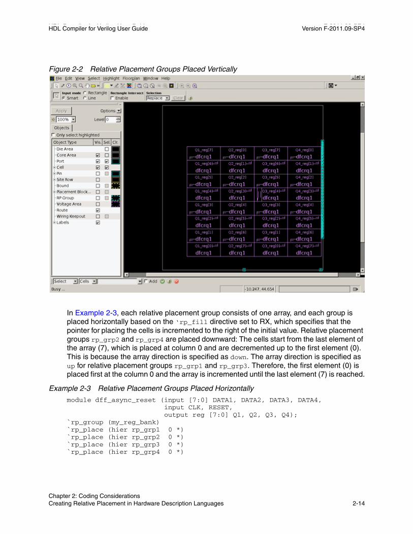
HDL Compiler for Verilog User Guide F-2011.09-SP4HDL Compiler for Verilog User Guide Version F-2011.09-SP4
Figure 2-2 Relative Placement Groups Placed Vertically
In Example 2-3, each relative placement group consists of one array, and each group is placed horizontally based on the ‘rp_fill directive set to RX, which specifies that the pointer for placing the cells is incremented to the right of the initial value. Relative placement groups rp_grp2 and rp_grp4 are placed downward: The cells start from the last element of the array (7), which is placed at column 0 and are decremented up to the first element (0). This is because the array direction is specified as down. The array direction is specified as up for relative placement groups rp_grp1 and rp_grp3. Therefore, the first element (0) is placed first at the column 0 and the array is incremented until the last element (7) is reached.
Example 2-3 Relative Placement Groups Placed Horizontally
module dff_async_reset (input [7:0] DATA1, DATA2, DATA3, DATA4, input CLK, RESET, output reg [7:0] Q1, Q2, Q3, Q4);`rp_group (my_reg_bank)`rp_place (hier rp_grp1 0 *)`rp_place (hier rp_grp2 0 *)`rp_place (hier rp_grp3 0 *)`rp_place (hier rp_grp4 0 *)
Chapter 2: Coding Considerations Creating Relative Placement in Hardware Description Languages 2-14
HDL Compiler for Verilog User Guide Version F-2011.09-SP4
`rp_endgroup (my_reg_bank)
always @(posedge CLK or posedge RESET) begin `rp_group (rp_grp1) `rp_fill (0 0 RX) `rp_array_dir(up) `rp_endgroup (rp_grp1) if (RESET) Q1 <= 8'b0; else Q1 <= DATA1; end
always @(posedge CLK or posedge RESET) `rp_group (rp_grp2) `rp_fill (0 0 RX) `rp_array_dir(down) `rp_endgroup (rp_grp2) if (RESET) Q2 <= 8'b0; else Q2 <= DATA2;
always @(posedge CLK or posedge RESET) `rp_group (rp_grp3) `rp_fill (0 0 RX) `rp_array_dir(up) `rp_endgroup (rp_grp3) if (RESET) Q3 <= 8'b0; else Q3 <= DATA3;
always @(posedge CLK or posedge RESET) `rp_group (rp_grp4) `rp_fill (0 0 RX) `rp_array_dir(down) `rp_endgroup (rp_grp4) if (RESET) Q4 <= 8'b0; else Q4 <= DATA4;endmodule
Chapter 2: Coding Considerations Creating Relative Placement in Hardware Description Languages 2-15Chapter 2: Coding Considerations Creating Relative Placement in Hardware Description Languages 2-15

HDL Compiler for Verilog User Guide F-2011.09-SP4HDL Compiler for Verilog User Guide Version F-2011.09-SP4
Figure 2-2 shows the layout generated from Example 2-3. Each relative placement group consists of one array, and each group is placed horizontally.
Figure 2-3 Relative Placement Groups Placed Horizontally
General Coding Guidelines
The following sections provide general coding guidelines:
• Separate Sequential and Combinational Assignments
• Persistence of Values Across Calls to Tasks
• defparam
• Function Placed Within a Module
Chapter 2: Coding Considerations General Coding Guidelines 2-16
HDL Compiler for Verilog User Guide Version F-2011.09-SP4
Separate Sequential and Combinational AssignmentsTo compute values synchronously and store them in flip-flops, set up an always block with a signal edge trigger. To let other values change asynchronously, make a separate always block with no signal edge trigger. Put the assignments you want clocked in the always block with the signal edge trigger and the other assignments in the other always block. This technique is used for creating Mealy machines, such as the one in Example 2-4. Note that out changes asynchronously with in1 or in2.
Example 2-4 Mealy Machine
module mealy (in1, in2, clk, reset, out);input in1, in2, clk, reset;output out;reg current_state, next_state, out;
always @(posedge clk or negedge reset) // state vector flip-flops (sequential)
if (!reset)current_state = 0;
elsecurrent_state = next_state;
always @(in1 or in2 or current_state)// output and state vector decode (combinational)
case (current_state)0: begin
next_state = 1;out = 1'b0;
end1: if (in1) begin
next_state = 1'b0;out = in2;
endelse begin
next_state = 1'b1;out = !in2;
endendcase
endmodule
Persistence of Values Across Calls to Tasks In Verilog simulation, a local variable in a function or task has a static lifetime by default, which means that the memory for it is allocated only once, at the beginning of simulation, and the value most recently written to it is preserved from one call to the next. In synthesis,
Chapter 2: Coding Considerations General Coding Guidelines 2-17Chapter 2: Coding Considerations General Coding Guidelines 2-17
HDL Compiler for Verilog User Guide F-2011.09-SP4HDL Compiler for Verilog User Guide Version F-2011.09-SP4
HDL Compiler assumes by default that functions and tasks do not depend on these previous values and reinitializes all static variables in functions and tasks to unknowns at the beginning of each call.
Verilog code that does not conform to this synthesis assumption can yield a synthesis and simulation mismatch.You should declare all functions and tasks using the automatic keyword, which tells the simulator to allocate new memory for local variables at the beginning of each call.
defparam Usage of defparam is highly discouraged in synthesis because of ambiguity problems. Because of these problems, defparam is not supported inside generate blocks. For details, see the Verilog LRM.
Function Placed Within a ModuleYou can place a function within a module during a function call. However, you cannot place a function before or after a module. Placing it before or after the module generates error messages because HDL Compiler cannot see the function when analyzing the design.
Interacting With Other Flows
The design structure created by HDL Compiler can impact commands that are applied to the design at later steps. To enable these flows, some considerations are required during the HDL Compiler analyze and elaborate steps. The following sections provide information and guidelines to help enable later flows.
• Synthesis Flows
• Low-Power Flows
• Verification Flows
Synthesis Flows• Controlling Structure With Parentheses
• Multibit Components
Chapter 2: Coding Considerations Interacting With Other Flows 2-18
HDL Compiler for Verilog User Guide Version F-2011.09-SP4
Controlling Structure With Parentheses You can use parentheses to force the synthesis of parallel hardware. For example, the expression (A + B) + (C + D) builds an adder for A + B, an adder for C + D, and an adder to add the result. Design Compiler preserves the subexpressions dictated by the parentheses, but this restriction on Design Compiler optimizations might lead to less-than-optimum area and timing results.
Parentheses can also be helpful in coding for late-arriving signals. For example, if you are adding three signals—A, B, and C—and A is late arriving, then A + (B + C) can be useful in handling the late-arriving signal A. Note that Design Compiler will also try to create a structure to allow the late-arriving signal to meet timing. Any restriction on Design Compiler optimizations might lead to less-than-optimum area and timing results.
Multibit Components HDL Compiler can infer multibit components. If your technology library supports multibit components, they can offer several benefits, such as reduced area and power or a more regular structure for place and route. For details about inferring multibit components, see “infer_multibit and dont_infer_multibit” on page 7-9.
Low-Power FlowsThe following section provides HDL Compiler guidelines for keeping a signal name.
Keeping Signal NamesBy default, HDL Compiler performs optimizations, such as dead code elimination, unconnected logic, and so on, that remove nets defined in the RTL. If your downstream flow requires that you use one of these removed nets, you can give HDL Compiler guideline information for keeping a signal name by using the hdlin_keep_signal_name variable (default is all_driving) and the keep_signal_name directive. Table 2-1 describes the variable options.
Chapter 2: Coding Considerations Interacting With Other Flows 2-19Chapter 2: Coding Considerations Interacting With Other Flows 2-19
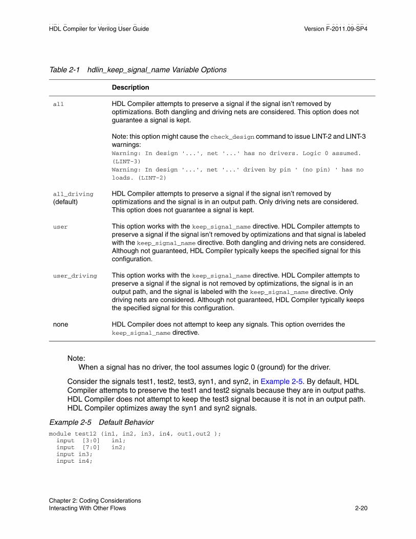
HDL Compiler for Verilog User Guide F-2011.09-SP4HDL Compiler for Verilog User Guide Version F-2011.09-SP4
Option Description
all HDL Compiler attempts to preserve a signal if the signal isn’t removed by optimizations. Both dangling and driving nets are considered. This option does not guarantee a signal is kept. Note: this option might cause the check_design command to issue LINT-2 and LINT-3 warnings: Warning: In design '...', net '...' has no drivers. Logic 0 assumed.
(LINT-3) Warning: In design '...', net '...' driven by pin ' (no pin) ' has no
loads. (LINT-2)
all_driving (default)
HDL Compiler attempts to preserve a signal if the signal isn’t removed by optimizations and the signal is in an output path. Only driving nets are considered. This option does not guarantee a signal is kept.
user This option works with the keep_signal_name directive. HDL Compiler attempts to preserve a signal if the signal isn’t removed by optimizations and that signal is labeled with the keep_signal_name directive. Both dangling and driving nets are considered. Although not guaranteed, HDL Compiler typically keeps the specified signal for this configuration.
user_driving This option works with the keep_signal_name directive. HDL Compiler attempts to preserve a signal if the signal is not removed by optimizations, the signal is in an output path, and the signal is labeled with the keep_signal_name directive. Only driving nets are considered. Although not guaranteed, HDL Compiler typically keeps the specified signal for this configuration.
none HDL Compiler does not attempt to keep any signals. This option overrides the keep_signal_name directive.
Note: When a signal has no driver, the tool assumes logic 0 (ground) for the driver.
Consider the signals test1, test2, test3, syn1, and syn2, in Example 2-5. By default, HDL Compiler attempts to preserve the test1 and test2 signals because they are in output paths. HDL Compiler does not attempt to keep the test3 signal because it is not in an output path. HDL Compiler optimizes away the syn1 and syn2 signals.
Example 2-5 Default Behaviormodule test12 (in1, in2, in3, in4, out1,out2 ); input [3:0] in1; input [7:0] in2; input in3; input in4;
Table 2-1 hdlin_keep_signal_name Variable Options
Chapter 2: Coding Considerations Interacting With Other Flows 2-20

HDL Compiler for Verilog User Guide Version F-2011.09-SP4
output reg [7:0] out1,out2;
wire test1,test2, test3, syn1,syn2;
//synopsys async_set_reset "in4" assign test1= ( in1[3] & ~in1[2] & in1[1] & ~in1[0] ); //test1 signal is in an input and output path assign test2= syn1+syn2; //test2 signal is in an output path, but it is not in an input path assign test3= in1 + in2; //test3 signal is in an input path, but it is not in an output path always @(in3 or in2 or in4 or test1) out2=test2+out1; always @(in3 or in2 or in4 or test1) if (in4) out1 = 8'h0; else if (in3 & test1) out1 = in2;endmodule
To keep the test3 signal, set hdlin_keep_signal_name to user and place the keep_signal_name directive on test3, as shown in Example 2-6.
Example 2-6 Keeping Signal Names// set the hdlin_keep_signal_name variable to usermodule ksn2 (in1, in2, in3, in4, out1,out2 ); input [3:0] in1; input [7:0] in2; input in3; input in4; output reg [7:0] out1,out2;
wire test1,test2, test3, syn1,syn2; //synopsys keep_signal_name "test1 test2 test3" //synopsys async_set_reset "in4" assign test1= ( in1[3] & ~in1[2] & in1[1] & ~in1[0] ); //test1 signal is in an input and output path assign test2= syn1+syn2; //test2 signal is in a output path, but it is not in an input path assign test3= in1 + in2; //test3 signal is in an input path, but it is not in an output path always @(in3 or in2 or in4 or test1) out2=test2+out1; always @(in3 or in2 or in4 or test1) if (in4) out1 = 8'h0; else if (in3 & test1) out1 = in2; endmodule
Chapter 2: Coding Considerations Interacting With Other Flows 2-21Chapter 2: Coding Considerations Interacting With Other Flows 2-21

HDL Compiler for Verilog User Guide F-2011.09-SP4HDL Compiler for Verilog User Guide Version F-2011.09-SP4
Table 2-2 shows how the variable settings affect the preservation of signals test1, test2, and test3, with and without the directive applied to it. Asterisks indicate that HDL Compiler does not attempt to keep the signal and might remove it.
Table 2-2 Variable and Directive Matrix for Signals test1, test2, and test3
hdlin_keep_signal_name = all none user user_driving all_driving
keep_signal_name is not set on test1
attempts to keep
* * * attempts to keep
keep_signal_name is set on test1
attempts to keep
* attempts to keep
attempts to keep
attempts to keep
keep_signal_name is not set on test2
attempts to keep
* * * attempts to keep
keep_signal_name is set on test2
attempts to keep
* attempts to keep
attempts to keep
attempts to keep
keep_signal_name is not set on test3 (Example 2-5)
attempts to keep
* * * *
keep_signal_name is set on test3 (Example 2-6)
attempts to keep
* attempts to keep
* *
Verification FlowsThe following section provides simulation-related coding information and information about simulation and synthesis mismatch issues.
Simulation/Synthesis Mismatch IssuesSimulation/synthesis mismatch issues are described in the following sections:
• one_hot and one_cold Directives
• full_case and parallel_case Directives
• D Flip-Flop With Synchronous and Asynchronous Load
• Variable Part-Select Operator
• Sets and Resets
Chapter 2: Coding Considerations Interacting With Other Flows 2-22

HDL Compiler for Verilog User Guide Version F-2011.09-SP4
• Three-State Inference
• Asynchronous Design Verification
• Comparisons to x or z Values
• Timing Specifications
• Sensitivity Lists
• Initial States for Variables
one_hot and one_cold Directives
A simulation/synthesis mismatch can occur if you use the one_hot and one_cold directives in your RTL but your design does not meet the requirements for their usage. See “one_hot” on page 7-15 and “one_cold” on page 7-15.
full_case and parallel_case Directives
A simulation/synthesis mismatch can occur if you use the full_case and parallel_case directives in your RTL but your design does not meet the requirements for their usage. See “full_case” on page 7-7 and “parallel_case” on page 7-15.
D Flip-Flop With Synchronous and Asynchronous Load
A simulation/synthesis mismatch can occur when inferring D flip-flops with synchronous and asynchronous loads. See “D Flip-Flop With Synchronous and Asynchronous Load” on page 4-20.
Variable Part-Select Operator
A simulation/synthesis mismatch can occur if you select bits from an array that are not valid. See “Part-Select Addressing Operators ([+:] and [-:])” on page B-35.
Sets and Resets
A simulation/synthesis mismatch can occur if the set/reset signal is masked by an X during initialization in simulation. To reduce mismatches, use the sync_set_reset directive to label set/reset signals. See “sync_set_reset” on page 7-17.
Three-State Inference
When inferring three-state devices, do not use multiple always blocks. Multiple always blocks cause a simulation/synthesis mismatch because the reg data type is not resolved. See “Assigning Multiple Three-State Drivers to a Single Variable” on page 6-4.
Chapter 2: Coding Considerations Interacting With Other Flows 2-23Chapter 2: Coding Considerations Interacting With Other Flows 2-23
HDL Compiler for Verilog User Guide F-2011.09-SP4HDL Compiler for Verilog User Guide Version F-2011.09-SP4
Asynchronous Design Verification
In synchronous designs, all registers use the same clock signal, and the design has no combinational feedback paths, one-shots, or delay lines. If you use asynchronous design techniques, synthesis and simulation results might not agree. Because Design Compiler does not issue warning messages for asynchronous designs, you are responsible for verifying the correctness of your circuit.
The following examples show two approaches to the same counter design: Example 2-7 is synchronous, and Example 2-8 is asynchronous.
Example 2-7 Fully Synchronous Counter Design
module COUNT (RESET, ENABLE, CLK, Z);input RESET, ENABLE, CLK;output [2:0] Z;reg [2:0] Z; always @(posedge CLK) begin if (RESET) begin Z = 3'b0; end else if (ENABLE) begin Z = Z + 1'b1; end endendmodule
Example 2-8 Asynchronous Counter Design
module async_counter(enableCount, countOut);input enableCount;output [3:0] countOut;reg [3:0] countOut;
wire ready, increment;wire [9:0] tmp;
assign increment = enableCount & ready;
always @(increment or countOut)begin if (increment) begin countOut = countOut + 1; endend
// pulse generatorgenvar i;generate
Chapter 2: Coding Considerations Interacting With Other Flows 2-24
HDL Compiler for Verilog User Guide Version F-2011.09-SP4
for (i=0; i<9; i=i+1) begin: delay_chain IV delInv(tmp[i], tmp[i+1]); // lsi_10k.db library invert endendgenerateassign tmp[0] = increment;assign ready = tmp[9];
endmodule
Some forms of asynchronous behavior are not supported in an RTL coding style. For example, you might expect X = ~(A & (~(~(~A)))), a circuit description of a one-shot signal generator, to generate three inverters (an inverting delay line) and a NAND gate. However, this circuit description is optimized to X = A ~& (~ A) and then to X = 1.
If special care is not taken when synthesizing the design, the instantiated inverter chain will be optimized and the synthesized design will not function the same way as the RTL simulates because the timing relationship between ready and increment will not be preserved. In this case, dont_touch constraints on the inverters and manual timing checks will be required to ensure the functionality of the circuit.
Comparisons to x or z Values
HDL Compiler always evaluates comparisons to an x or a z as false. This behavior is different from simulation behavior and might cause a synthesis/simulation mismatch. To prevent such a mismatch, do not use don’t care values in comparisons.
To a simulator, an x or a z value is a distinct value, different from a 1 or a 0. In synthesis, however, an x or a z value becomes a 0 or a 1. When used in a comparison, HDL Compiler always evaluates the comparison to false. Because of this difference in treatment, the potential for a simulation/synthesis mismatch exists whenever a comparison is made with a don't care value.
For example,
if (a == 1'bx) ...
is synthesized as
if FALSE
The following case statement causes a synthesis/simulation mismatch because the simulator evaluates 2'b1x to match 11 and 10, but the synthesis tool evaluates 2'b1x to false; the same holds true for the 2'b0x- evaluation.
case (A) 2'b1x:... -- you want 2'b1x to match 11 and 10 but -- HDLC always evaluates this comparison -- to false 2'b0x:... -- you want 2'b0x to match 00 and 01 but -- HDLC always evaluates this comparison
Chapter 2: Coding Considerations Interacting With Other Flows 2-25Chapter 2: Coding Considerations Interacting With Other Flows 2-25

HDL Compiler for Verilog User Guide F-2011.09-SP4HDL Compiler for Verilog User Guide Version F-2011.09-SP4
-- to false default : ....endcase
HDL Compiler issues a warning similar to the following when it synthesizes such comparisons:
Warning: Comparison against '?', 'x', or 'z' values is always false. It may cause simulation/synthesis mismatch. (ELAB-310)
In Example 2-9, HDL Compiler always assigns 1 to B (and issues an ELAB-310 warning), because if (A == 1'bx) is always evaluated to false.
Example 2-9 Comparison to x Ignored
module test(A, B); input A; output reg B; always begin if (A == 1'bx) B = 0; else B = 1; endendmodule
Timing Specifications
HDL Compiler ignores all timing controls because these controls cannot be realized in logic. In general, you can safely include timing control information in your description if it does not change the value clocked into a flip-flop. That is, the delay must be less than the clock period; otherwise, synthesis might disagree with simulation.
You can assign a delay value in a wire or wand declaration, and you can use the Verilog keywords scalared and vectored for simulation. HDL Compiler accepts the syntax of these constructs, but they are ignored when the circuit is synthesized.
Sensitivity Lists
If all the signals read within the always block are not listed in the sensitivity list, HDL Compiler generates a warning similar to the following:
Warning: Variable ’myvar’ is being read in block ’bar’ declared on line 88 but does not occur in the timing control of the block.
The circuit synthesized by HDL Compiler is sensitive to all signals within the block, even if they are not listed in the sensitivity list. This differs from simulator behavior, which relies on the list. To prevent synthesis/simulation mismatches, follow these guidelines when developing the sensitivity list:
Chapter 2: Coding Considerations Interacting With Other Flows 2-26

HDL Compiler for Verilog User Guide Version F-2011.09-SP4
• For sequential logic, include the clock signal and all asynchronous control signals in the sensitivity list.
• For combinational logic, be sure that all inputs are in the sensitivity list.
HDL Compiler supports the Verilog 2001 construct, always @*, which provides a convenient way to ensure that all variables are listed.
HDL Compiler ignores sensitivity lists that do not contain an edge expression, and builds the logic as if all variables within the always block were contained in the sensitivity list. When any edge expressions are listed in the sensitivity list, no nonedge expressions can be listed. HDL Compiler issues an error message if you try to mix edge expressions and ordinary variables in the sensitivity list.
When the sensitivity list does not contain an edge expression, combinational logic is usually generated, although latches might be generated if the variable is not fully specified, that is, if the variable is not assigned on every path through the block.
Note: The statements @ (posedge clock) and @ (negedge clock) are not supported in functions or tasks.
Initial States for Variables
For functions and tasks, any local reg variables are initialized to 0, and values of output ports are not preserved across calls. In simulators, values are typically preserved. This difference in behavior often causes a synthesis/simulation mismatch. See “Persistence of Values Across Calls to Tasks” on page 2-17.
Chapter 2: Coding Considerations Interacting With Other Flows 2-27Chapter 2: Coding Considerations Interacting With Other Flows 2-27
HDL Compiler for Verilog User Guide F-2011.09-SP4HDL Compiler for Verilog User Guide Version F-2011.09-SP4
Chapter 2: Coding Considerations Interacting With Other Flows 2-28

3Modeling Combinational Logic 3
Logic circuits can be divided into two general classes:
• Combinational – The value of the output depends only on the values of the input signals.
• Sequential – The value of the output depends only on the values of the input signals and the previous condition on the circuit.
This chapter discusses combinational logic synthesis in the following sections:
• Synthetic Operators
• Logic and Arithmetic Expressions
• Multiplexing Logic
• MUX_OP Components With Variable Indexing
• Modeling Complex MUX Inferences: Bit and Memory Accesses
• Bit-Truncation Coding for DC Ultra Datapath Extraction
• Latches in Combinational Logic
3-1

HDL Compiler for Verilog User Guide F-2011.09-SP4HDL Compiler for Verilog User Guide Version F-2011.09-SP4
Synthetic Operators
Synopsys provides a collection of intellectual property (IP), referred to as the DesignWare Basic IP Library, to support the synthesis products. Basic IP provides basic implementations of common arithmetic functions that can be referenced by HDL operators in your RTL source code.
The DesignWare paradigm is built on a hierarchy of abstractions. HDL operators (either built-in operators like + and *, or HDL functions and procedures) are associated with synthetic operators, which are bound in turn to synthetic modules. Each synthetic module can have multiple architectural realizations, called implementations. When you use the HDL addition operator in a design description, HDL Compiler infers the need for an adder resource and puts an abstract representation of the addition operation into your circuit netlist. The same holds true when you instantiate a DesignWare component. For example, an instantiation of DW01_add will be mapped to the synthetic operator associated with it. See Figure 3-1 on page 3-3.
A synthetic library contains definitions for synthetic operators, synthetic modules, and bindings. It also contains declarations that associate synthetic modules with their implementations.
To display information about the standard synthetic library that is included with a Design Compiler license, use the report_synlib command:
report_synlib standard.sldb
For more information about DesignWare synthetic operators, modules, and libraries, see the DesignWare documentation.
Chapter 3: Modeling Combinational Logic Synthetic Operators 3-2

HDL Compiler for Verilog User Guide Version F-2011.09-SP4
Figure 3-1 DesignWare Hierarchy
Implementations
Bindings
map_to_operator directive
HDL operator HDL operator definition
Synthetic operator
Synthetic modules
Implementation
declarations
ADD_UNS_OP
proprietarycarry-lookaheadripple
ALUADDADD_SUB
Synthetic library
Design library
Z <= X + Y
Chapter 3: Modeling Combinational Logic Synthetic Operators 3-3Chapter 3: Modeling Combinational Logic Synthetic Operators 3-3
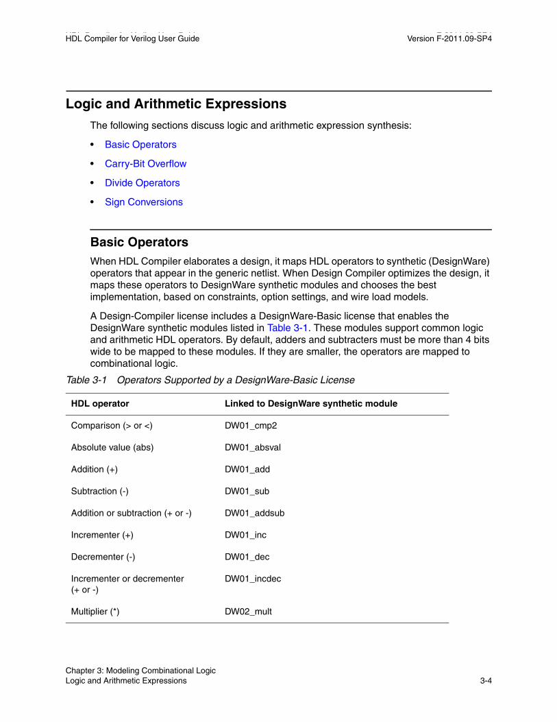
HDL Compiler for Verilog User Guide F-2011.09-SP4HDL Compiler for Verilog User Guide Version F-2011.09-SP4
Logic and Arithmetic Expressions
The following sections discuss logic and arithmetic expression synthesis:
• Basic Operators
• Carry-Bit Overflow
• Divide Operators
• Sign Conversions
Basic OperatorsWhen HDL Compiler elaborates a design, it maps HDL operators to synthetic (DesignWare) operators that appear in the generic netlist. When Design Compiler optimizes the design, it maps these operators to DesignWare synthetic modules and chooses the best implementation, based on constraints, option settings, and wire load models.
A Design-Compiler license includes a DesignWare-Basic license that enables the DesignWare synthetic modules listed in Table 3-1. These modules support common logic and arithmetic HDL operators. By default, adders and subtracters must be more than 4 bits wide to be mapped to these modules. If they are smaller, the operators are mapped to combinational logic.
Table 3-1 Operators Supported by a DesignWare-Basic License
HDL operator Linked to DesignWare synthetic module
Comparison (> or <) DW01_cmp2
Absolute value (abs) DW01_absval
Addition (+) DW01_add
Subtraction (-) DW01_sub
Addition or subtraction (+ or -) DW01_addsub
Incrementer (+) DW01_inc
Decrementer (-) DW01_dec
Incrementer or decrementer (+ or -)
DW01_incdec
Multiplier (*) DW02_mult
Chapter 3: Modeling Combinational Logic Logic and Arithmetic Expressions 3-4

HDL Compiler for Verilog User Guide Version F-2011.09-SP4
Carry-Bit Overflow When Design Compiler performs arithmetic optimization, it considers how to handle the overflow from carry bits during addition. The optimized structure is affected by the bit-widths you declare for storing intermediate results. For example, suppose you write an expression that adds two 4-bit numbers and stores the result in a 4-bit register. If the result of the addition overflows the 4-bit output, the most significant bits are truncated. Example 3-1 shows how overflow characteristics are handled.
Example 3-1 Adding Numbers of Different Bit-Widths
t <= a + b; // a and b are 4-bit numbersz <= t + c; // c is a 6-bit number
In Example 3-1, three variables are added (a + b + c). A temporary variable, t, holds the intermediate result of a + b. Suppose t is declared as a 4-bit variable, so the overflow bits from the addition of a + b are truncated. HDL Compiler determines the default structure, which is shown in Figure 3-2.
Figure 3-2 Default Structure With 4-Bit Temporary Variable
a[4] b[4]
c[6]
z[6]
t[4]
Now suppose the addition is performed without a temporary variable (z = a + b + c). HDL Compiler determines that 5 bits are needed to store the intermediate result of the addition, so no overflow condition exists. The results of the final addition might be different from the first case, where a 4-bit temporary variable is declared that truncates the result of the intermediate addition. Therefore, these two structures do not always yield the same result. The structure for the second case is shown in Figure 3-3.
Chapter 3: Modeling Combinational Logic Logic and Arithmetic Expressions 3-5Chapter 3: Modeling Combinational Logic Logic and Arithmetic Expressions 3-5

HDL Compiler for Verilog User Guide F-2011.09-SP4HDL Compiler for Verilog User Guide Version F-2011.09-SP4
Figure 3-3 Structure With 5-Bit Intermediate Result
a[4] b[4]
c[6]
z[6]
[5]
Now suppose the expression is optimized for delay and that signal a arrives late. Design Compiler restructures the expression so that b and c are added first. Because c is declared as a 6-bit number, Design Compiler determines that the intermediate result must be stored in a 6-bit variable. The structure for this case, where signal a arrives late, is shown in Figure 3-4. Note how this expression differs from the structure in Figure 3-2.
Figure 3-4 Structure for Late-Arriving Signal
a[4]
b[4] c[6]
z[6]
[6]
Divide OperatorsHDL Compiler supports division where the operands are not constant, such as in Example 3-2, by instantiating a DesignWare divider, as shown in Figure 3-5. Note that when you compile a design that contains an inferred divider, you must have a DesignWare license in addition to the DesignWare-Basic license.
Chapter 3: Modeling Combinational Logic Logic and Arithmetic Expressions 3-6
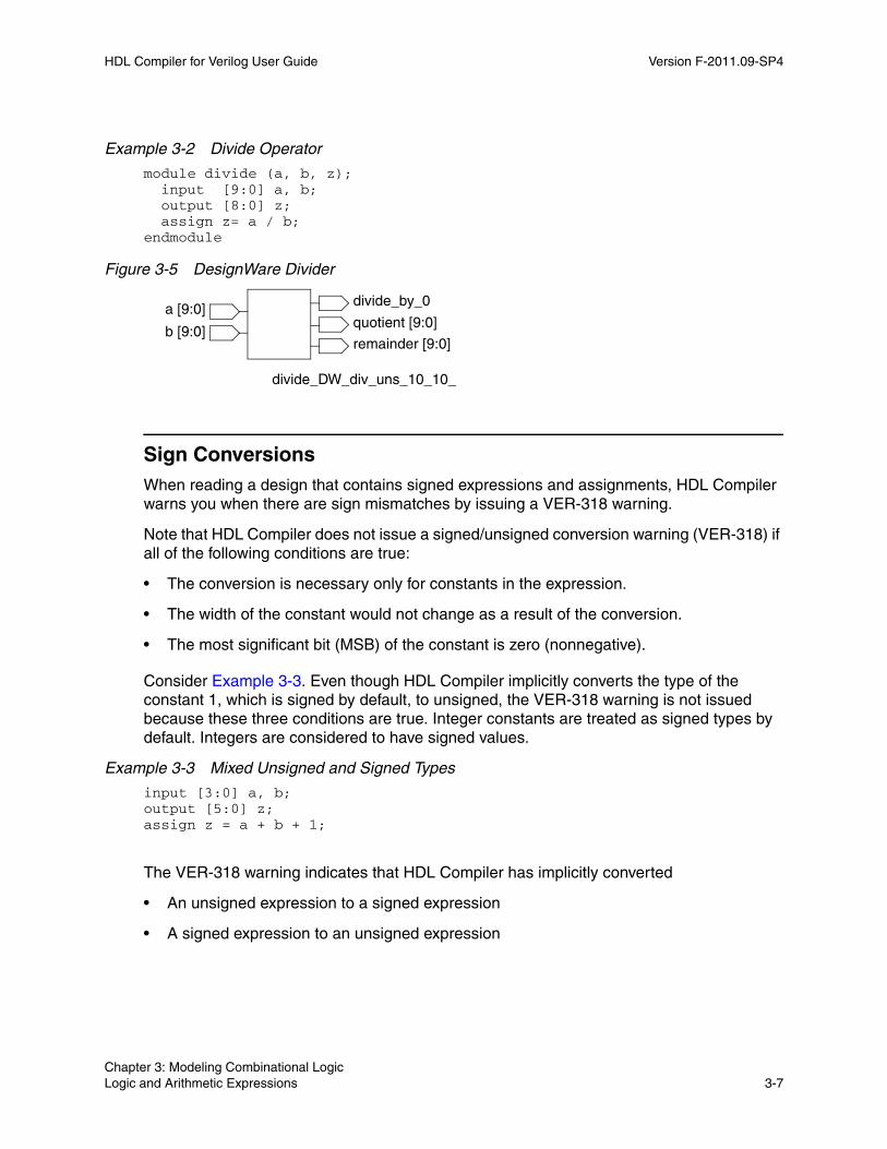
HDL Compiler for Verilog User Guide Version F-2011.09-SP4
Example 3-2 Divide Operator
module divide (a, b, z); input [9:0] a, b; output [8:0] z; assign z= a / b;endmodule
Figure 3-5 DesignWare Divider
a [9:0]
b [9:0] remainder [9:0]
quotient [9:0]
divide_by_0
divide_DW_div_uns_10_10_
Sign Conversions When reading a design that contains signed expressions and assignments, HDL Compiler warns you when there are sign mismatches by issuing a VER-318 warning.
Note that HDL Compiler does not issue a signed/unsigned conversion warning (VER-318) if all of the following conditions are true:
• The conversion is necessary only for constants in the expression.
• The width of the constant would not change as a result of the conversion.
• The most significant bit (MSB) of the constant is zero (nonnegative).
Consider Example 3-3. Even though HDL Compiler implicitly converts the type of the constant 1, which is signed by default, to unsigned, the VER-318 warning is not issued because these three conditions are true. Integer constants are treated as signed types by default. Integers are considered to have signed values.
Example 3-3 Mixed Unsigned and Signed Types
input [3:0] a, b;output [5:0] z;assign z = a + b + 1;
The VER-318 warning indicates that HDL Compiler has implicitly converted
• An unsigned expression to a signed expression
• A signed expression to an unsigned expression
Chapter 3: Modeling Combinational Logic Logic and Arithmetic Expressions 3-7Chapter 3: Modeling Combinational Logic Logic and Arithmetic Expressions 3-7
HDL Compiler for Verilog User Guide F-2011.09-SP4HDL Compiler for Verilog User Guide Version F-2011.09-SP4
or, it has assigned
• An unsigned right side to a signed left side
• A signed right side to an unsigned left side
For example, in this code,
reg signed [3:0] a; reg [7:0] c;
a = 4'sb1010;c = a+7'b0101011;
an implicit signed/unsigned conversion occurs—the signed operand a is converted to an unsigned value, and the VER-318 warning “signed to unsigned conversion occurs” is issued. Note that a will not be sign-extended. This behavior is in accordance with the Verilog 2001 standard.
When explicit type casting is used, conversion warnings are not issued. For example, in the preceding code, to force a to be unsigned, you assign c as follows:
c = $unsigned(a)+7'b0101011;
no warning is issued.
Consider the following assignment:
reg [7:0] a;
a = 4'sb1010;
A VER-318 warning “signed to unsigned assignment occurs” is issued when this code is read. Although the left side is unsigned, the right side will still be sign-extended; that is, a will have the value 8'b11111010 after the assignment.
If a line contains more than one implicit conversion, such as the expression assigned to c in the following example, only one warning message is issued.
reg signed [3:0] a;reg signed [3:0] b;reg signed [7:0] c;
c = a+4'b0101+(b*3'b101);
In this example, a and b are converted to unsigned values, and because the whole right side is unsigned, assigning the right-side value to c also results in the warning.
Chapter 3: Modeling Combinational Logic Logic and Arithmetic Expressions 3-8
HDL Compiler for Verilog User Guide Version F-2011.09-SP4
The code in Example 3-4 generates eight VER-318 warnings shown in Example 3-5.
Example 3-4 Modules m1 Through m9
1module m1 (a, z); 2 input signed [0:3] a; 3 output signed [0:4] z; 4 assign z = a; 5endmodule 6 7 8module m2 (a, z); 9 input signed [0:2] a; 10 output [0:4] z; 11 assign z = a + 3'sb111; 12endmodule 13 14 15module m3 (a, z); 16 input [0:3] a; 17 output z; 18 reg signed [0:3] x; 19 reg z; 20 always begin 21 x = a; 22 z = x < 4'sd5; /* note that x is signed and compared to 4'sd5, which is also signed, but the result of the comparison is put into z, an unsigned reg. This appears to be a sign mismatch; however, no VER-318 warning is issued for this line because comparison results are always considered unsigned. This is true for all relational operators. */ 23 end 24endmodule 25 26 27module m4 (in1, in2, out); 28 input signed [7:0] in1, in2; 29 output signed [7:0] out; 30 assign out = in1 * in2; 31endmodule 32 33 34module m5 (a, b, z); 35 input [1:0] a, b; 36 output [2:0] z; 37 wire signed [1:0] x = a; 38 wire signed [1:0] y = b; 39 assign z = x - y; 40endmodule 41 42 43module m6 (a, z); 44 input [3:0] a; 45 output z;
Chapter 3: Modeling Combinational Logic Logic and Arithmetic Expressions 3-9Chapter 3: Modeling Combinational Logic Logic and Arithmetic Expressions 3-9

HDL Compiler for Verilog User Guide F-2011.09-SP4HDL Compiler for Verilog User Guide Version F-2011.09-SP4
46 reg signed [3:0] x; 47 wire z; 48 always @(a) begin 49 x = a; 50 end 51 assign z = x < -4'sd5; 52endmodule 53 54module m7 (in1, in2, lt, in1_lt_64); 55 input signed [7:0] in1, in2; // two signed inputs 56 output lt, in1_lt_64; 57 assign lt = in1 < in2; // comparison is signed 58 59 // using a signed constant results in a signed comparison 60 61 assign in1_lt_64 = in1 < 8'sd64; 62endmodule 63 64 65module m8 (in1, in2, lt); 66 67// in1 is signed but in2 is unsigned 68 69 input signed [7:0] in1; 70 input [7:0] in2; 71 output lt; 72 wire uns_lt, uns_in1_lt_64; 73 74/* comparison is unsigned because of the sign mismatch; in1 is signed but in2 is unsigned */ 75 76 assign uns_lt = in1 < in2; 77 78/* Unsigned constant causes unsigned comparison; so negative values of in1 would compare as larger than 8'd64 */ 79 80 assign uns_in1_lt_64 = in1 < 8'd64; 81 assign lt = uns_lt + uns_in1_lt_64; 82 83endmodule 84 85 86 87module m9 (in1, in2, lt); 88 input signed [7:0] in1; 89 input [7:0] in2; 90 output lt; 91 assign lt = in1 < $signed ({1'b0, in2}); 92endmodule 93 94
Chapter 3: Modeling Combinational Logic Logic and Arithmetic Expressions 3-10
HDL Compiler for Verilog User Guide Version F-2011.09-SP4
The eight VER-318 warnings generated by the code in Example 3-4 are shown in Example 3-5.
Example 3-5 Sign Conversion Warnings for m1 Through m9
Warning: /usr/00budgeting/vhdl-mr/warn-sign.v:11: signed to unsigned assignment occurs. (VER-318)Warning: /usr/00budgeting/vhdl-mr/warn-sign.v:21: unsigned to signed assignment occurs. (VER-318)Warning: /usr/00budgeting/vhdl-mr/warn-sign.v:37: unsigned to signed assignment occurs. (VER-318)Warning: /usr/00budgeting/vhdl-mr/warn-sign.v:38: unsigned to signed assignment occurs. (VER-318)Warning: /usr/00budgeting/vhdl-mr/warn-sign.v:39: signed to unsigned assignment occurs. (VER-318)Warning: /usr/00budgeting/vhdl-mr/warn-sign.v:49: unsigned to signed assignment occurs. (VER-318)Warning: /usr/00budgeting/vhdl-mr/warn-sign.v:76: signed to unsigned conversion occurs. (VER-318)Warning: /usr/00budgeting/vhdl-mr/warn-sign.v:80: signed to unsigned conversion occurs. (VER-318)HDLC compilation completed successfully.Current design is now ’/usr/00budgeting/vhdl-mr/m1.db:m1’m1 m2 m3 m4 m5 m6 m7 m8 m9
Table 3-2 describes what caused the warnings listed in Example 3-5.
Table 3-2 Causes of Sign Mismatch Warnings (VER-318)
Module Cause of warning
m1, m4, and m7 These modules do not have any sign conversion warnings because the signs are consistently applied.
m9 This module does not generate a VER-318 warning because, even though in1 and in2 are sign mismatched, the casting operator is used to force the sign on in2. When a casting operator is used, no warning is returned when sign conversion occurs.
m2 In this module, a is signed and added to 3'sb111, which is signed and has a value of -1. However, z is not signed, so the value of the expression on the right, which is signed, will be converted to unsigned when assigned to z. The VER-318 warning “signed to unsigned assignment occurs” is issued.
Chapter 3: Modeling Combinational Logic Logic and Arithmetic Expressions 3-11Chapter 3: Modeling Combinational Logic Logic and Arithmetic Expressions 3-11
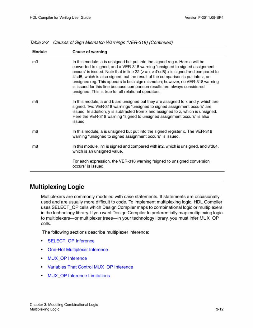
HDL Compiler for Verilog User Guide F-2011.09-SP4HDL Compiler for Verilog User Guide Version F-2011.09-SP4
Multiplexing Logic
Multiplexers are commonly modeled with case statements. If statements are occasionally used and are usually more difficult to code. To implement multiplexing logic, HDL Compiler uses SELECT_OP cells which Design Compiler maps to combinational logic or multiplexers in the technology library. If you want Design Compiler to preferentially map multiplexing logic to multiplexers—or multiplexer trees—in your technology library, you must infer MUX_OP cells.
The following sections describe multiplexer inference:
• SELECT_OP Inference
• One-Hot Multiplexer Inference
• MUX_OP Inference
• Variables That Control MUX_OP Inference
• MUX_OP Inference Limitations
m3 In this module, a is unsigned but put into the signed reg x. Here a will be converted to signed, and a VER-318 warning “unsigned to signed assignment occurs” is issued. Note that in line 22 (z = x < 4'sd5) x is signed and compared to 4'sd5, which is also signed, but the result of the comparison is put into z, an unsigned reg. This appears to be a sign mismatch; however, no VER-318 warning is issued for this line because comparison results are always considered unsigned. This is true for all relational operators.
m5 In this module, a and b are unsigned but they are assigned to x and y, which are signed. Two VER-318 warnings “unsigned to signed assignment occurs” are issued. In addition, y is subtracted from x and assigned to z, which is unsigned. Here the VER-318 warning “signed to unsigned assignment occurs” is also issued.
m6 In this module, a is unsigned but put into the signed register x. The VER-318 warning “unsigned to signed assignment occurs” is issued.
m8 In this module, in1 is signed and compared with in2, which is unsigned, and 8‘d64, which is an unsigned value. For each expression, the VER-318 warning “signed to unsigned conversion occurs” is issued.
Table 3-2 Causes of Sign Mismatch Warnings (VER-318) (Continued)
Module Cause of warning
Chapter 3: Modeling Combinational Logic Multiplexing Logic 3-12

HDL Compiler for Verilog User Guide Version F-2011.09-SP4
SELECT_OP Inference By default, HDL Compiler uses SELECT_OP components to implement conditional operations implied by if and case statements. An example of a SELECT_OP cell implementation for an 8-bit data signal is shown in Figure 3-6.
Figure 3-6 SELECT_OP Implementation for an 8-bit Data Signal
output
DATA7
DATA6
DATA5
DATA4
DATA3
DATA2
CONT
DATA8
CONT
CONT
CONT
CONT
CONT
CONT
CONT
For an 8-bit data signal, 8 selection bits are needed. This is called a one-hot implementation.
data signals
select signals
DATA1z_
SELECT_OPs behave like one-hot multiplexers; the control lines are mutually exclusive, and each control input allows the data on the corresponding data input to pass to the output of the cell. To determine which data signal is chosen, HDL Compiler generates selection logic, as shown in Figure 3-7.
Chapter 3: Modeling Combinational Logic Multiplexing Logic 3-13Chapter 3: Modeling Combinational Logic Multiplexing Logic 3-13
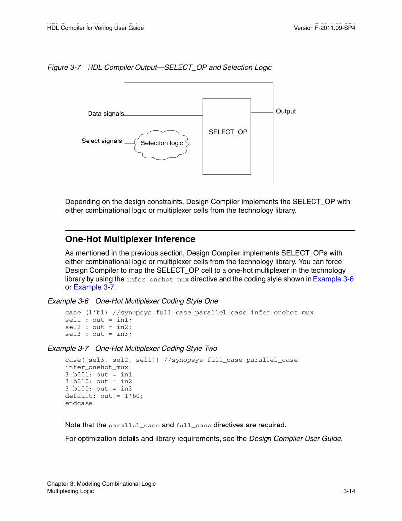
HDL Compiler for Verilog User Guide F-2011.09-SP4HDL Compiler for Verilog User Guide Version F-2011.09-SP4
Figure 3-7 HDL Compiler Output—SELECT_OP and Selection Logic
Selection logicSelect signalsSELECT_OP
Data signals Output
Depending on the design constraints, Design Compiler implements the SELECT_OP with either combinational logic or multiplexer cells from the technology library.
One-Hot Multiplexer InferenceAs mentioned in the previous section, Design Compiler implements SELECT_OPs with either combinational logic or multiplexer cells from the technology library. You can force Design Compiler to map the SELECT_OP cell to a one-hot multiplexer in the technology library by using the infer_onehot_mux directive and the coding style shown in Example 3-6 or Example 3-7.
Example 3-6 One-Hot Multiplexer Coding Style One
case (1'b1) //synopsys full_case parallel_case infer_onehot_muxsel1 : out = in1;sel2 : out = in2;sel3 : out = in3;
Example 3-7 One-Hot Multiplexer Coding Style Two
case({sel3, sel2, sel1}) //synopsys full_case parallel_case infer_onehot_mux3'b001: out = in1;3'b010: out = in2;3'b100: out = in3;default: out = 1'b0;endcase
Note that the parallel_case and full_case directives are required.
For optimization details and library requirements, see the Design Compiler User Guide.
Chapter 3: Modeling Combinational Logic Multiplexing Logic 3-14
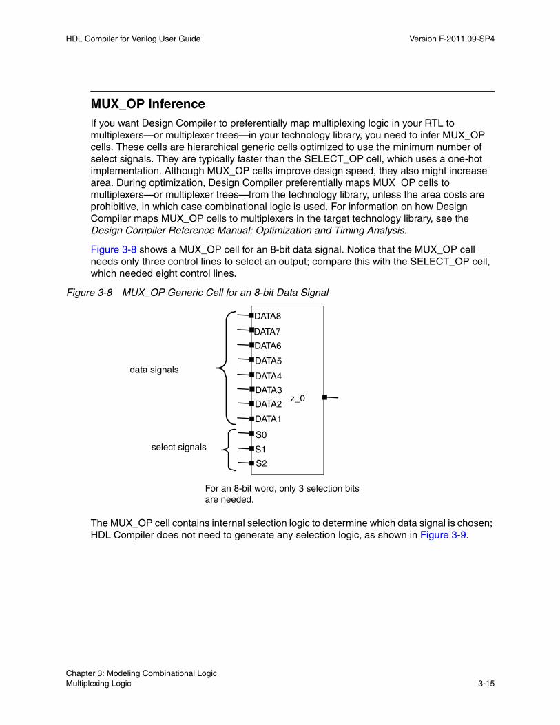
HDL Compiler for Verilog User Guide Version F-2011.09-SP4
MUX_OP InferenceIf you want Design Compiler to preferentially map multiplexing logic in your RTL to multiplexers—or multiplexer trees—in your technology library, you need to infer MUX_OP cells. These cells are hierarchical generic cells optimized to use the minimum number of select signals. They are typically faster than the SELECT_OP cell, which uses a one-hot implementation. Although MUX_OP cells improve design speed, they also might increase area. During optimization, Design Compiler preferentially maps MUX_OP cells to multiplexers—or multiplexer trees—from the technology library, unless the area costs are prohibitive, in which case combinational logic is used. For information on how Design Compiler maps MUX_OP cells to multiplexers in the target technology library, see the Design Compiler Reference Manual: Optimization and Timing Analysis.
Figure 3-8 shows a MUX_OP cell for an 8-bit data signal. Notice that the MUX_OP cell needs only three control lines to select an output; compare this with the SELECT_OP cell, which needed eight control lines.
Figure 3-8 MUX_OP Generic Cell for an 8-bit Data Signal
data signals
select signals
For an 8-bit word, only 3 selection bits are needed.
DATA7
DATA6
DATA5
DATA4
DATA3
DATA2
DATA1
S0
DATA8
S1
z_0
S2
The MUX_OP cell contains internal selection logic to determine which data signal is chosen; HDL Compiler does not need to generate any selection logic, as shown in Figure 3-9.
Chapter 3: Modeling Combinational Logic Multiplexing Logic 3-15Chapter 3: Modeling Combinational Logic Multiplexing Logic 3-15

HDL Compiler for Verilog User Guide F-2011.09-SP4HDL Compiler for Verilog User Guide Version F-2011.09-SP4
Figure 3-9 HDL Compiler Output—MUX_OP Generic Cell for 8-Bit Data
Select signalsMUX_OP
Data signals Output
Use the following methods to infer MUX_OP cells:
• To infer MUX_OP cells for a specific case or if statement, use the infer_mux directive. Additionally, you must use a simple variable as the control expression; for example, you can use the input “A” but not the negation of input “A”. If statements have special coding considerations, for details “Considerations When Using If Statements to Code For MUX_OPs” on page 3-22.
always@(SEL) begin case (SEL) // synopsys infer_mux 2'b00: DOUT <= DIN[0]; 2'b01: DOUT <= DIN[1]; 2'b10: DOUT <= DIN[2]; 2'b11: DOUT <= DIN[3]; endcase
Note that the case statement must be parallel; otherwise, a MUX_OP is not inferred and an error is reported. The parallel_case directive does not make a case statement truly parallel. This directive can also be set on a block to direct HDL Compiler to infer MUX_OPs for all case statements in that block. Use the following syntax:
// synopsys infer_mux block_label_list
• To infer MUX_OP cells for all case and if statements, use the hdlin_infer_mux variable. Additionally, your coding style must use a simple variable as the control expression; for example, you can use the input “A” but not the negation of input “A”.
By default, if you set the infer_mux directive on a case statement that has two or more synthetic (DesignWare) operators as data inputs, HDL Compiler generates an ELAB-370 warning and does not infer a MUX_OP because you would lose the benefit of resource sharing.
Chapter 3: Modeling Combinational Logic Multiplexing Logic 3-16
HDL Compiler for Verilog User Guide Version F-2011.09-SP4
For detailed information about MUX_OP components, see the Design Compiler Reference Manual: Optimization and Timing Analysis.
Variables That Control MUX_OP InferenceThe variables that control MUX_OP cell inference are listed in Table 3-3.
Table 3-3 MUX_OP Inference Variables
Variable Description
hdlin_infer_mux This variable controls MUX_OP inference for all designs you input in the same Design Compiler session.
Options:
• default—Infers MUX_OPs for case and if statements in processes that have the infer_mux directive or attribute attached.
• none—Does not infer MUX_OPs, regardless of the directives set in the VHDL description. HDL Compiler generates a warning if hdlin_infer_mux = none and infer_mux are used in the RTL.
• all—Infers MUX_OPs for every case and if statement in your design for which one can be used. This can negatively affect the quality of results, because it might be more efficient to implement the MUX_OPs as random logic instead of using a specialized multiplexer structure.
hdlin_mux_size_limit
This variable sets the maximum size of a MUX_OP that HDL Compiler can infer. The default value is 32. If you set this variable to a value greater than 32, HDL Compiler may take an unusually long elaboration time.
If the number of branches in a case statement exceeds the maximum size specified by this variable, HDL Compiler generates the following message:
Warning: A mux was not inferred because case statement
%s has a very large branching factor. (HDL-383)
hdlin_mux_size_min Sets the minimum number of data inputs for a MUX_OP inference. Default value is 2.
hdlin_mux_oversize_ ratio
Defined as the ratio of the number of MUX_OP inputs to the unique number of data inputs. When this ratio is exceeded, a MUX_OP will not be inferred and the circuit will be generated with SELECT_OPs. Default value is 100.
Chapter 3: Modeling Combinational Logic Multiplexing Logic 3-17Chapter 3: Modeling Combinational Logic Multiplexing Logic 3-17
HDL Compiler for Verilog User Guide F-2011.09-SP4HDL Compiler for Verilog User Guide Version F-2011.09-SP4
MUX_OP Inference ExamplesIn Example 3-8, two MUX_OPs and one SELECT_OP are inferred, as follows:
• For the first always block, the infer_mux directive is set on the case statement, which causes HDL Compiler to infer a MUX_OP.
• For the second always block, there are two case statements.
❍ For the first case statement, a SELECT_OP is inferred. This is the default inference.
❍ However, the second case statement has the infer_mux directive set on it, which causes HDL Compiler to infer the MUX_OP cell.
Example 3-8 Two MUX_OPs and One SELECT_OP Inferred
module test_muxop_selectop (DIN1, DIN2, DIN3, SEL1, SEL2, SEL3, DOUT1,DOUT2, DOUT3); input [7:0] DIN1, DIN2; input [3:0] DIN3; input [2:0] SEL1, SEL2; input [1:0] SEL3;
hdlin_mux_size_only To ensure that MUX_OP cells are mapped to MUX technology cells, you must apply a size_only attribute to the cells to prevent logic decomposition in later optimization steps. You can set the size_only attribute on each MUX_OP manually or allow the tool to set it automatically. The automatic behavior can be controlled by the hdlin_mux_size_only variable.
Options:
• 0–Specifies that no cells receive the size_only attribute.
• 1–Specifies that MUX_OP cells that are generated with the RTL infer_mux compiler directive and that are on set/reset signals receive the size_only attribute. This is the default setting.
• 2–Specifies that all MUX_OP cells that are generated with the RTL infer_mux compiler directive receive the size_only attribute.
• 3–Specifies that all MUX_OP cells on set/reset signals receive the size_only attribute: for example, MUX_OP cells that are generated by setting the hdlin_infer_mux variable to all.
• 4–Specifies that all MUX_OP cells receive the size_only attribute: for example, MUX_OP cells that are generated by the hdlin_infer_mux variable set to all.
By default, the hdlin_mux_size_only variable is set to 1, meaning that MUX_OP cells that are generated with the RTL infer_mux compiler directive and that are on set/reset signals receive the size_only attribute.
Table 3-3 MUX_OP Inference Variables (Continued)
Variable Description
Chapter 3: Modeling Combinational Logic Multiplexing Logic 3-18
HDL Compiler for Verilog User Guide Version F-2011.09-SP4
output DOUT1, DOUT2, DOUT3;
reg DOUT1, DOUT2, DOUT3;
always @ (SEL1 or DIN1)begin case (SEL1) //synopsys infer_mux 3'b000: DOUT1 <= DIN1[0]; 3'b001: DOUT1 <= DIN1[1]; 3'b010: DOUT1 <= DIN1[2]; 3'b011: DOUT1 <= DIN1[3]; 3'b100: DOUT1 <= DIN1[4]; 3'b101: DOUT1 <= DIN1[5]; 3'b110: DOUT1 <= DIN1[6]; 3'b111: DOUT1 <= DIN1[7]; endcaseend
always @ (SEL2 or SEL3 or DIN2 or DIN3)begin case (SEL2) 3'b000: DOUT2 <= DIN2[0]; 3'b001: DOUT2 <= DIN2[1]; 3'b010: DOUT2 <= DIN2[2]; 3'b011: DOUT2 <= DIN2[3]; 3'b100: DOUT2 <= DIN2[4]; 3'b101: DOUT2 <= DIN2[5]; 3'b110: DOUT2 <= DIN2[6]; 3'b111: DOUT2 <= DIN2[7]; endcase
case (SEL3) //synopsys infer_mux 2'b00: DOUT3 <= DIN3[0]; 2'b01: DOUT3 <= DIN3[1]; 2'b10: DOUT3 <= DIN3[2]; 2'b11: DOUT3 <= DIN3[3];
endcaseend
endmodule
Example 3-9 shows the MUX_OP inference report for the code in Example 3-8. Figure 3-10 on page 3-20 shows a representation of the HDL Compiler implementation. The tool displays inference reports by default. If you do not want these reports displayed, you can turn them off using the hdlin_reporting_level variable. For more information about the hdlin_reporting_level variable, see “Elaboration Reports” on page 1-7.
Chapter 3: Modeling Combinational Logic Multiplexing Logic 3-19Chapter 3: Modeling Combinational Logic Multiplexing Logic 3-19

HDL Compiler for Verilog User Guide F-2011.09-SP4HDL Compiler for Verilog User Guide Version F-2011.09-SP4
Example 3-9 MUX_OP Inference ReportStatistics for case statements in always block at line 31 in file ...===============================================| Line | full/ parallel |===============================================| 33 | auto/auto |===============================================Statistics for MUX_OPs=================================================================| block name/line | Inputs | Outputs | # sel inputs | MB |=================================================================| test_muxop_selectop/13 | 8 | 1 | 3 | N || test_muxop_selectop/47 | 4 | 1 | 2 | N |=================================================================
The first column of the MUX_OP report indicates the block that contains the case statement for which the MUX_OP is inferred. The line number of the case statement in Verilog also appears in this column. The remaining columns indicate the number of inputs, outputs, and select lines on the inferred MUX_OP.
Figure 3-10 HDL Compiler Implementation
MUX_OP
MUX_OP
SELECT_OP
DIN1
DIN2
DIN3
SEL2
SEL1
SEL3
DOUT3
DOUT2
DOUT1
selection logic
Example 3-10 uses the infer_mux directive for a specific block.
Example 3-10 MUX_OP Inference for a Block
module muxtwo(DIN1, DIN2, SEL1, SEL2, DOUT1, DOUT2); input [7:0] DIN1; input [3:0] DIN2;
Chapter 3: Modeling Combinational Logic Multiplexing Logic 3-20
HDL Compiler for Verilog User Guide Version F-2011.09-SP4
input [2:0] SEL1; input [1:0] SEL2; output DOUT1, DOUT2; reg DOUT1, DOUT2;
//synopsys infer_mux "blk1"
always @(SEL1 or SEL2 or DIN1 or DIN2)begin: blk1 // this case statement infers an 8-to-1 MUX_OP case (SEL1) 3'b000: DOUT1 <= DIN1[0]; 3'b001: DOUT1 <= DIN1[1]; 3'b010: DOUT1 <= DIN1[2]; 3'b011: DOUT1 <= DIN1[3]; 3'b100: DOUT1 <= DIN1[4]; 3'b101: DOUT1 <= DIN1[5]; 3'b110: DOUT1 <= DIN1[6]; 3'b111: DOUT1 <= DIN1[7]; endcase
// this case statement infers a 4-to-1 MUX_OP case (SEL2) 2'b00: DOUT2 <= DIN2[0]; 2'b01: DOUT2 <= DIN2[1]; 2'b10: DOUT2 <= DIN2[2]; 2'b11: DOUT2 <= DIN2[3]; endcaseendendmodule
Example 3-11 uses the infer_mux directive for a specific case statement. This case statement contains eight unique values, and HDL Compiler infers an 8-to-1 MUX_OP.
Example 3-11 MUX_OP Inference for a Specific case Statement
module mux8to1 (DIN, SEL, DOUT); input [7:0] DIN; input [2:0] SEL; output DOUT; reg DOUT; always@(SEL or DIN) begin: blk1 case (SEL) // synopsys infer_mux 3'b000: DOUT <= DIN[0]; 3'b001: DOUT <= DIN[1]; 3'b010: DOUT <= DIN[2]; 3'b011: DOUT <= DIN[3]; 3'b100: DOUT <= DIN[4]; 3'b101: DOUT <= DIN[5]; 3'b110: DOUT <= DIN[6]; 3'b111: DOUT <= DIN[7]; endcase
Chapter 3: Modeling Combinational Logic Multiplexing Logic 3-21Chapter 3: Modeling Combinational Logic Multiplexing Logic 3-21
HDL Compiler for Verilog User Guide F-2011.09-SP4HDL Compiler for Verilog User Guide Version F-2011.09-SP4
endendmodule
In Example 3-12 a MUX_OP is inferred by using an if-else statement. This coding style requires the control expression to be a simple variable. If statements have special coding considerations, for details see “Considerations When Using If Statements to Code For MUX_OPs” on page 3-22.
Example 3-12 MUX_OP Inference Using if-else Statement
module test ( input sel,a,b, output reg dout); always @(*) if(sel) //synopsys infer_mux dout = a; else dout = b;endmodule
In Example 3-13 a MUX_OP is inferred by using a “?:” operator. This coding style requires you to place the infer_mux directive just after “?” construct.
Example 3-13 MUX_OP Inference for a Specific case Statement
module test (sig, A, B, C); input A, B, C; output sig; assign sig = A ? /* synopsys infer_mux */ B :C ;endmodule
Considerations When Using If Statements to Code For MUX_OPs In general, good coding practice is to use case statements when coding multiplexing logic because the if statement coding style can result in potentially slower, larger designs and reduce coding flexibility. These issues are described in this section.
In order for HDL Compiler to infer MUX_OPs through if-else statements, you must use very simple expressions, such as those shown in Example 3-14. From this code, the tool can infer a 4-to-1 MUX_OP cell.
Example 3-14 Tool Infers MUX_OP From If-Else Statements
module mux41 (a, b, c, d, sel, dout); input a, b, c, d; input [1:0] sel; output reg dout;
always@(*) begin if (sel == 2'b00) /* synopsys infer_mux */ begin dout <= a; end
Chapter 3: Modeling Combinational Logic Multiplexing Logic 3-22
HDL Compiler for Verilog User Guide Version F-2011.09-SP4
else if (sel == 2'b01) begin dout <= b; end else if (sel == 2'b10) begin dout <= c; end else if (sel == 2'b11) begin dout <= d; end
end
endmodule
In Example 3-14, the code specifies all possible conditions and the tool builds the most efficient logic, a 4-to-1 MUX_OP cell. However, when your if statements don't cover all possible conditions, as in Example 3-15, the tool does not infer optimum logic. Instead, it infers a 4-to-1 multiplexer even though there are only two branches. In this case, the optimum logic is a 2-to-1 MUX_OP cell, but the tool builds a 4-to-1 MUX_OP.
Example 3-15 Tool Infers Inefficient 4:1 MUX_OP From If-Else Statements
module mux21 (a, b, sel, dout); input a, b; input [1:0] sel; output reg dout;
always@(*) begin if (sel == 2'b00) /* synopsys infer_mux */ begin dout <= a; end else begin dout <= b; end end
endmodule
In order to infer a 2-to-1 MUX_OP cell, you must re-code the design in Example 3-15 to the style shown in Example 3-16.
Example 3-16 Tool Infers 2:1 MUX_OP From If-Else Statements
module mux21 (a, b, sel, dout); input a, b; input [1:0] sel; output reg dout;
reg tmp;
always@(*) begin tmp = (sel == 2'b11) ? 1'b1 : 1'b0;
Chapter 3: Modeling Combinational Logic Multiplexing Logic 3-23Chapter 3: Modeling Combinational Logic Multiplexing Logic 3-23
HDL Compiler for Verilog User Guide F-2011.09-SP4HDL Compiler for Verilog User Guide Version F-2011.09-SP4
if (tmp) /* synopsys infer_mux */ begin dout <= a; end else begin dout <= b; end end
endmodule
Another difficulty with using if statements is limited coding flexibility. Expressions like the one used in Example 3-17 are too complex for HDL Compiler to handle. In Example 3-17, HDL Compiler does not infer a MUX_OP cell even when the infer_mux directive is used. Instead, the tool infers a SELECT_OP to build the multiplexing logic. In order to infer a 2-to-1 MUX_OP cell, you must re-code to extract the expression of the if statement and assign it to a variable so that the behavior is like a case statement.
Example 3-17 Tool Cannot Infer MUX_OP From Complex Expressions
module mux21 (a, b, c, d, sel, dout); input a, b, c, d; input [1:0] sel; output reg dout;
always@(*) begin if (sel[0] == 1'b0) /* synopsys infer_mux */ begin dout <= a & b; end else begin dout <= d & c; end endendmodule
To further illustrate the expression coding requirements, consider Example 3-18. From the code in Example 3-18, the tool infers a SELECT_OP even though the infer_mux directive is used. To enable the tool to infer a MUX_OP cell, you must re-code the design in Example 3-18 to the style shown in Example 3-19.
Example 3-18 Tool Infers SELECT_OP for Multiplexing Logic From Complex Expressions
module mux41 (a, b, c, d, dout); input a, b, c, d; output reg dout;
always@(*) begin if (a == 1'b0 && b == 1'b0) /* synopsys infer_mux */ begin dout <= c & d; end
Chapter 3: Modeling Combinational Logic Multiplexing Logic 3-24
HDL Compiler for Verilog User Guide Version F-2011.09-SP4
else if (a == 1'b0 && b == 1'b1) begin dout <= c | d; end else if (a == 1'b1 && b == 1'b0) begin dout <= !c & d; end else if (a == 1'b1 && b == 1'b1) begin dout <= c | !d; end endendmodule
Example 3-19 Tool Infers MUX_OP for Multiplexing Logic
module mux41 (a, b, c, d, dout); input a, b, c, d; output reg dout; reg [1:0] tmp;
always@(*) begin tmp = {a, b}; if (tmp == 2'b00) /* synopsys infer_mux */ begin dout <= c & d; end else if (tmp == 2'b01) begin dout <= c | d; end else if (tmp == 2'b10) begin dout <= !c & d; end else if (tmp == 2'b11) begin dout <= c | !d; end endendmodule
A good practice, whenever possible, is to use case statements instead of if-else statements when you want to infer MUX_OP cells.
MUX_OP Inference LimitationsHDL Compiler does not infer MUX_OP cells for
• case statements in while loops
• case statements embedded in an always block
• case or if statements that use complex control expressions
Chapter 3: Modeling Combinational Logic Multiplexing Logic 3-25Chapter 3: Modeling Combinational Logic Multiplexing Logic 3-25
HDL Compiler for Verilog User Guide F-2011.09-SP4HDL Compiler for Verilog User Guide Version F-2011.09-SP4
You must use a simple variable as the control expression; for example, you can use the input “A” but the not the negation of input “A.”
MUX_OP cells are inferred for incompletely specified case statements, such as case statements that
• Contain an if statement that covers more than one value
• Have a missing case statement branch or a missing assignment in a case statement branch
• Contain don’t care values (x or "-")
In these cases, the logic might not be optimum, because other optimizations are disabled when you infer MUX_OP cells under these conditions. For example, HDL Compiler optimizes default branches. If the infer_mux attribute is on the case statement, this optimization is not done.
When inferring a MUX_OP for an incompletely specified case statement, HDL Compiler generates the following ELAB-304 warning:
Warning: Case statement has an infer_mux attribute and a default branch or incomplete mapping. This can cause nonoptimal logic if a mux is inferred. (ELAB-304)
MUX_OP Components With Variable Indexing
HDL Compiler generates MUX_OP components to implement indexing into a data variable, using a variable address. For example,
module E(data, addr, out); input [7:0] data; input [2:0] addr; output out; assign out = data[addr]; endmodule
In this example, a MUX_OP is used to implement data[addr] because the subscript, addr, is not a known constant.
Modeling Complex MUX Inferences: Bit and Memory Accesses
In addition to inferring multiplexers from case statements, you can infer them for bit or memory accesses. See Example 3-20 through Example 3-21 for templates. By default, HDL Compiler uses a MUX_OP for bit and memory access.
Chapter 3: Modeling Combinational Logic MUX_OP Components With Variable Indexing 3-26
HDL Compiler for Verilog User Guide Version F-2011.09-SP4
Example 3-20 MUX Inference for Bit Access
module mux_infer_bit (x, a, y); input [15:0] x; input [3:0] a; output y; reg y; always @(x,a) begin
y = x[a]; endendmodule
Example 3-21 MUX Inference for Memory Access
module mux_infer_memory (rw, addr, data); input rw; input [3:0] addr; inout [15:0] data; reg [3:0] x [15:0]; assign data = (rw) ? x[addr] : 16'hz ;
always @(rw, data) if (!rw) x[addr] = data ;endmodule
Bit-Truncation Coding for DC Ultra Datapath Extraction
Datapath design is commonly used in applications that contain extensive data manipulation, such as 3-D, multimedia, and digital signal processing (DSP). Datapath extraction transforms arithmetic operators into datapath blocks to be implemented by a datapath generator.
The DC Ultra tool enables datapath extraction after timing-driven resource sharing and explores various datapath and resource-sharing options during compile.
Note: This feature is not available in DC Expert. See the Design Compiler documentation for datapath optimization details.
As of release 2002.05, DC Ultra datapath optimization supports datapath extraction of expressions containing truncated operands unless both of the following two conditions exist:
• The operands have upper bits truncated. For example, if d is 16-bits wide, d[7:0] truncates the upper eight bits.
• The width of the resulting expression is greater than the width of the truncated operand. For example, in the following statement, if e is 9-bits wide, the width of e is greater than the width of the truncated operand d[7:0]:
assign e = c + d[7:0];
Chapter 3: Modeling Combinational Logic Bit-Truncation Coding for DC Ultra Datapath Extraction 3-27Chapter 3: Modeling Combinational Logic Bit-Truncation Coding for DC Ultra Datapath Extraction 3-27
HDL Compiler for Verilog User Guide F-2011.09-SP4HDL Compiler for Verilog User Guide Version F-2011.09-SP4
Note that both conditions must be true to prevent extraction. For lower-bit truncations, the datapath is extracted in all cases.
Bit truncation can be either explicit or implicit. The following table describes both types of truncation.
Truncation type Description
Explicit bit truncation An explicit upper-bit truncation occurs when you specify the bit range for truncation.
The following code indicates explicit upper-bit truncation of operand A:
wire [i : 0] A;
out = A [j : 0]; // where j < i
Implicit bit truncation An implicit upper-bit truncation is one that occurs through assignment. Unlike with explicit upper-bit truncation, here you do not explicitly define the range for truncation.
The following code indicates implicit upper-bit truncation of operand Y:
input [7 : 0] A,B;
wire [14:0] Y = A * B;
Because A and B are each 8 bits wide, their product will be 16 bits wide. However, Y, which is only 15 bits wide, is assigned to be the 16-bit product, when the most significant bit (MSB) of the product is implicitly truncated. In this example, the MSB is the carryout bit.
To see how bit truncation affects datapath extraction, consider the code in Example 3-22.
Example 3-22 Design test1: Truncated Operand Is Extracted
module test1 (a,b,c,e); input [7:0] a,b,c; output [7:0] e; wire [14:0] d; assign d = a * b; // <--- implicit upper-bit truncation assign e = c + d; // width of e is less than dendmodule
In Example 3-22, the upper bits of the a * b operation are implicitly truncated when assigned to d, and the width of e is less than the width of d. This code meets the first condition on page 27 but does not meet the second. Because both conditions must be met to prevent extraction, this code is extracted.
Consider the code in Example 3-23. Here bit truncation prevents extraction.
Chapter 3: Modeling Combinational Logic Bit-Truncation Coding for DC Ultra Datapath Extraction 3-28

HDL Compiler for Verilog User Guide Version F-2011.09-SP4
Example 3-23 Design test2: Truncated Operand Is Not Extracted
module test2 (a,b,c,e); input [7:0] a,b,c; output [8:0] e; // <--- e is 9-bits wide wire [7:0] d; // <--- d is 8-bits wide assign d = a * b; // <---implicit upper-bit truncation assign e = c + d; // <---width of e is greater than dendmodule
In Example 3-23, the upper bits of the a * b operation are implicitly truncated when assigned to d, and the width of e is greater than the width of d. This code meets both the first and second conditions; the code is not extracted.
Consider the code in Example 3-24. Here bit truncation prevents extraction.
Example 3-24 Design test3: Truncated Operand Is Not Extractedmodule test3 (a,b,c,e); input [7:0] a,b,c; output [8:0] e; wire [15:0] d; // <--- d is 16-bits wide assign d = a * b; // <--- d is not truncated assign e = c + d[7:0]; // <--- explicit upper-bit truncation of d // width of e is greater than d[7:0]endmodule
In Example 3-24, the upper bits of d are explicitly truncated, and the width of e is greater than the width of d. This code meets both the first and second conditions; the code is not extracted.
Consider the code in Example 3-25. Here bit truncation does not prevent extraction.
Example 3-25 Design test4: Truncated Operand Is Extractedmodule test4 (a,b,c,e); input [7:0] a,b,c; output [9:0] e; wire [15:0] d; assign d = a * b; // <--- No implicit upper-bit truncation assign e = c + d[15:8]; // <---"explicit lower" bit truncation of d endmodule
In Example 3-25, the lower bits of d are explicitly truncated. For expressions involving lower-bit truncations, the truncated operands are extracted regardless of the bit-widths of the truncated operands and of the expression result; this code is extracted.
Chapter 3: Modeling Combinational Logic Bit-Truncation Coding for DC Ultra Datapath Extraction 3-29Chapter 3: Modeling Combinational Logic Bit-Truncation Coding for DC Ultra Datapath Extraction 3-29
HDL Compiler for Verilog User Guide F-2011.09-SP4HDL Compiler for Verilog User Guide Version F-2011.09-SP4
Latches in Combinational Logic
Sometimes your Verilog source can imply combinational feedback paths or latches in synthesized logic. This happens when a signal or a variable in a combinational logic block (an always block without a posedge or negedge clock statement) is not fully specified. A variable or signal is fully specified when it is assigned under all possible conditions.
When a variable is not assigned a value for all paths through an always block, the variable is conditionally assigned and a latch is inferred for the variable to store its previous value. To avoid these latches, make sure that the variable is fully assigned in all paths. In Example 3-26, the variable Q is not assigned if GATE equals 1’b0. Therefore, it is conditionally assigned and HDL Compiler creates a latch to hold its previous value.
Example 3-26 Latch Inference Using an if Statement
always @ (DATA or GATE) begin if (GATE) begin Q = DATA; endend
Example 3-27 and Example 3-28 show Q fully assigned—Q is assigned 0 when GATE equals 1’b0. Note that Example 3-27 and Example 3-28 are not equivalent to Example 3-26, in which Q holds its previous value when GATE equals 1’b0.
Example 3-27 Avoiding Latch Inference—Method 1
always @ (DATA, GATE) begin Q = 0; if (GATE) Q = DATA;end
Example 3-28 Avoiding Latch Inference—Method 2
always @ (DATA, GATE) begin if (GATE) Q = DATA; else Q = 0;end
The code in Example 3-29 results in a latch because the variable is not fully assigned. To avoid the latch inference, add the following statement before the endcase statement:
default: decimal= 10’b0000000000;
Chapter 3: Modeling Combinational Logic Latches in Combinational Logic 3-30
HDL Compiler for Verilog User Guide Version F-2011.09-SP4
Example 3-29 Latch Inference Using a case Statement
always @(I) begin case(I) 4'h0: decimal= 10'b0000000001; 4'h1: decimal= 10'b0000000010; 4'h2: decimal= 10'b0000000100; 4'h3: decimal= 10'b0000001000; 4'h4: decimal= 10'b0000010000; 4'h5: decimal= 10'b0000100000; 4'h6: decimal= 10'b0001000000; 4'h7: decimal= 10'b0010000000; 4'h8: decimal= 10'b0100000000; 4'h9: decimal= 10'b1000000000; endcaseend
Latches are also synthesized whenever a for loop statement does not assign a variable for all possible executions of the for loop and when a variable assigned inside the for loop is not assigned a value before entering the enclosing for loop.
Chapter 3: Modeling Combinational Logic Latches in Combinational Logic 3-31Chapter 3: Modeling Combinational Logic Latches in Combinational Logic 3-31

HDL Compiler for Verilog User Guide F-2011.09-SP4HDL Compiler for Verilog User Guide Version F-2011.09-SP4
Chapter 3: Modeling Combinational Logic Latches in Combinational Logic 3-32

4Modeling Sequential Logic 4
This chapter describes latch and flip-flop inference in the following sections:
• Generic Sequential Cells (SEQGENs)
• Inference Reports for Registers
• Register Inference Guidelines
• Register Inference Examples
Synopsys uses the term register to refer to a 1-bit memory device, either a latch or a flip-flop. A latch is a level-sensitive memory device. A flip-flop is an edge-triggered memory device.
4-1
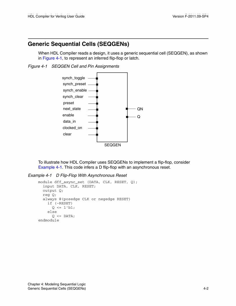
HDL Compiler for Verilog User Guide F-2011.09-SP4HDL Compiler for Verilog User Guide Version F-2011.09-SP4
Generic Sequential Cells (SEQGENs)
When HDL Compiler reads a design, it uses a generic sequential cell (SEQGEN), as shown in Figure 4-1, to represent an inferred flip-flop or latch.
Figure 4-1 SEQGEN Cell and Pin Assignments
SEQGEN
synch_toggle
QN
synch_preset
synch_enable
synch_clear
preset
next_state
enable
data_in
clocked_on
clear
Q
To illustrate how HDL Compiler uses SEQGENs to implement a flip-flop, consider Example 4-1. This code infers a D flip-flop with an asynchronous reset.
Example 4-1 D Flip-Flop With Asynchronous Reset
module dff_async_set (DATA, CLK, RESET, Q); input DATA, CLK, RESET; output Q; reg Q; always @(posedge CLK or negedge RESET) if (~RESET) Q <= 1'b1; else Q <= DATA;endmodule
Chapter 4: Modeling Sequential Logic Generic Sequential Cells (SEQGENs) 4-2
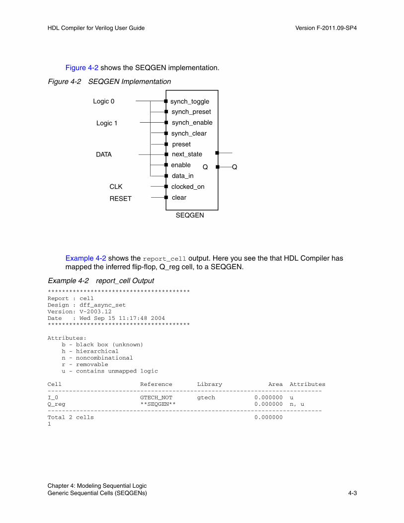
HDL Compiler for Verilog User Guide Version F-2011.09-SP4
Figure 4-2 shows the SEQGEN implementation.
Figure 4-2 SEQGEN Implementation
synch_toggle
synch_preset
synch_enable
synch_clear
preset
next_state
enable
data_in
clocked_on
clear
Q
RESET
CLK
DATA
Q
Logic 0
Logic 1
SEQGEN
Example 4-2 shows the report_cell output. Here you see the that HDL Compiler has mapped the inferred flip-flop, Q_reg cell, to a SEQGEN.
Example 4-2 report_cell Output****************************************Report : cellDesign : dff_async_setVersion: V-2003.12Date : Wed Sep 15 11:17:48 2004****************************************
Attributes: b - black box (unknown) h - hierarchical n - noncombinational r - removable u - contains unmapped logic
Cell Reference Library Area Attributes-----------------------------------------------------------------------------I_0 GTECH_NOT gtech 0.000000 uQ_reg **SEQGEN** 0.000000 n, u-----------------------------------------------------------------------------Total 2 cells 0.0000001
Chapter 4: Modeling Sequential Logic Generic Sequential Cells (SEQGENs) 4-3Chapter 4: Modeling Sequential Logic Generic Sequential Cells (SEQGENs) 4-3

HDL Compiler for Verilog User Guide F-2011.09-SP4HDL Compiler for Verilog User Guide Version F-2011.09-SP4
Example 4-3 shows the GTECH netlist.
Example 4-3 GTECH Netlist
module dff_async_set ( DATA, CLK, RESET, Q ); input DATA; input CLK; input RESET; output Q; wire \*Logic1* , \*Logic0* , N0;
\**SEQGEN** Q_reg ( .clear(1’b0), .preset(N0), .next_state(DATA), .clocked_on(CLK), .data_in(1’b0), .enable(1’b0), .Q(Q), .synch_clear( 1’b0), .synch_preset(1’b0), .synch_toggle(1’b0), .synch_enable(1’b1) ); GTECH_NOT I_0 ( .A(RESET), .Z(N0) );endmodule
After Design Compiler compiles the design, the SEQGEN is mapped to the appropriate flip-flop in the technology library. Figure 4-3 shows an example of an implementation after compile.
Figure 4-3 Design Compiler Implementation
Q_reg
data_in
clocked_on
clearQ
RESET
CLKQ
DATA
Note: If the technology library does not contain the inferred flip-flop or latch, Design Compiler creates combinational logic for the missing function, if possible. For example, if you infer a D flip-flip with a synchronous set but your target technology library does not contain this type of flip-flop, Design Compiler will create combinational logic for the synchronous set function. Design Compiler cannot create logic to duplicate an asynchronous preset/reset. Your library must contain the sequential cell with the asynchronous control pins. See “Register Inference Limitations” on page 4-13.
Chapter 4: Modeling Sequential Logic Generic Sequential Cells (SEQGENs) 4-4

HDL Compiler for Verilog User Guide Version F-2011.09-SP4
Inference Reports for Registers
HDL Compiler provides inference reports that describe each inferred flip-flop or latch. You can enable or disable the generation of inference reports by using the hdlin_reporting_level variable. By default, hdlin_reporting_level is set to basic. When hdlin_reporting_level is set to basic or comprehensive, HDL Compiler generates a report similar to Example 4-4. This basic inference report shows only which type of register was inferred.
Example 4-4 Inference Report for a D Flip-Flop With Asynchronous Reset==============================================================================| Register Name | Type | Width | Bus | MB | AR | AS | SR | SS | ST |==============================================================================| Q_reg | Flip-flop | 1 | N | N | Y | N | N | N | N |==============================================================================
In the report, the columns are abbreviated as follows:
• MB represents multibit cell
• AR represents asynchronous reset
• AS represents asynchronous set
• SR represents synchronous reset
• SS represents synchronous set
• ST represents synchronous toggle
A “Y” in a column indicates that the respective control pin was inferred for the register; an “N” indicates that the respective control pin was not inferred for the register. For a D flip-flop with an asynchronous reset, there should be a “Y” in the AR column. The report also indicates the type of register inferred, latch or flip-flop, and the name of the inferred cell.
When the hdlin_reporting_level variable is set to verbose, the report indicates how each pin of the SEQGEN cell is assigned, along with which type of register was inferred. Example 4-5 shows a verbose inference report.
Chapter 4: Modeling Sequential Logic Inference Reports for Registers 4-5Chapter 4: Modeling Sequential Logic Inference Reports for Registers 4-5

HDL Compiler for Verilog User Guide F-2011.09-SP4HDL Compiler for Verilog User Guide Version F-2011.09-SP4
Example 4-5 Verbose Inference Report for a D Flip-Flop With Asynchronous Reset==============================================================================| Register Name | Type | Width | Bus | MB | AR | AS | SR | SS | ST |==============================================================================| Q_reg | Flip-flop | 1 | N | N | Y | N | N | N | N |==============================================================================Sequential Cell (Q_reg)
Cell Type: Flip-FlopMultibit Attribute: NClock: CLKAsync Clear: RESETAsync Set: 0Async Load: 0Sync Clear: 0Sync Set: 0Sync Toggle: 0Sync Load: 1
If you do not want inference reports, set hdlin_reporting_level to none. For more information about the hdlin_reporting_level variable, see “Elaboration Reports” on page 1-7.
Register Inference Guidelines
When inferring registers, restrict each always block so that it infers a single type of memory element and check the inference report to verify that HDL Compiler inferred the correct device.
Register inference guidelines are described in the following sections:
• Multiple Events in an always Block
• Minimizing Registers
• Keeping Unloaded Registers
• Preventing Unwanted Latches: hdlin_check_no_latch
• Register Inference Limitations
Multiple Events in an always BlockHDL Compiler supports multiple events in a single always block, as shown in Example 4-6.
Example 4-6 Multiple Events in a Single always Block
module test( data, clk, sum) ; input [7:0]data; input clk; output [7:0]sum;
Chapter 4: Modeling Sequential Logic Register Inference Guidelines 4-6

HDL Compiler for Verilog User Guide Version F-2011.09-SP4
reg [7:0]sum; always begin @ (posedge clk) sum = data; @ (posedge clk) sum = sum + data; @ (posedge clk) ; sum = sum + data; end endmodule
Minimizing RegistersAn always block that contains a clock edge in the sensitivity list causes HDL Compiler to infer a flip-flop for each variable assigned a value in that always block. It might not be necessary to infer as flip-flops all variables in the always block. Make sure your HDL description builds only as many flip-flops as the design requires.
Example 4-7 infers six flip-flops: three to hold the values of count and one each to hold and_bits, or_bits, and xor_bits. However, the values of the outputs and_bits, or_bits, and xor_bits depend solely on the value of count. Because count is registered, there is no reason to register the three outputs.
Example 4-7 Inefficient Circuit Description With Six Inferred Registers
module count (clock, reset, and_bits, or_bits, xor_bits); input clock, reset; output and_bits, or_bits, xor_bits; reg and_bits, or_bits, xor_bits;
reg [2:0] count;
always @(posedge clock) beginif (reset) count = 0;else count = count + 1;
and_bits = & count;or_bits = | count;xor_bits = ^ count;
endendmodule
Chapter 4: Modeling Sequential Logic Register Inference Guidelines 4-7Chapter 4: Modeling Sequential Logic Register Inference Guidelines 4-7
HDL Compiler for Verilog User Guide F-2011.09-SP4HDL Compiler for Verilog User Guide Version F-2011.09-SP4
Example 4-8 shows the inference report which contains the six inferred flip-flops.
Example 4-8 Inference Report===============================================================================| Register Name | Type | Width | Bus | MB | AR | AS | SR | SS | ST |===============================================================================| or_bits_reg | Flip-flop | 1 | N | N | N | N | N | N | N || count_reg | Flip-flop | 3 | Y | N | N | N | N | N | N || xor_bits_reg | Flip-flop | 1 | N | N | N | N | N | N | N || and_bits_reg | Flip-flop | 1 | N | N | N | N | N | N | N |===============================================================================
To avoid inferring extra registers, you can assign the outputs from within an asynchronous always block. Example 4-9 shows the same function described with two always blocks, one synchronous and one asynchronous, that separate registered or sequential logic from combinational logic. This technique is useful for describing finite state machines. Signal assignments in the synchronous always block are registered, but signal assignments in the asynchronous always block are not. The code in Example 4-9 creates a more area-efficient design.
Example 4-9 Circuit With Three Inferred Registers
module count (clock, reset, and_bits, or_bits, xor_bits); input clock, reset; output and_bits, or_bits, xor_bits; reg and_bits, or_bits, xor_bits;
reg [2:0] count;
always @(posedge clock) begin//synchronous blockif (reset)
count = 0;else
count = count + 1;endalways @(count) begin//asynchronous block
and_bits = & count;or_bits = | count;xor_bits = ^ count;
endendmodule
Example 4-10 shows the inference report, which contains three inferred flip-flops.
Example 4-10 Inference Report=============================================================================| Register Name | Type | Width | Bus | MB | AR | AS | SR | SS | ST |=============================================================================| count_reg | Flip-flop | 3 | Y | N | N | N | N | N | N |=============================================================================
Chapter 4: Modeling Sequential Logic Register Inference Guidelines 4-8
HDL Compiler for Verilog User Guide Version F-2011.09-SP4
Keeping Unloaded Registers HDL Compiler does not automatically keep unloaded or undriven flip-flops or latches in a design. These cells are determined to be unnecessary and are removed during optimization. You can use the hdlin_preserve_sequential variable to control which cells to preserve:
• To preserve unloaded/undriven flip-flops and latches in your GTECH netlist, set hdlin_preserve_sequential to all.
• To preserve all unloaded flip-flops only, set hdlin_preserve_sequential to ff.
• To preserve all unloaded latches only, set hdlin_preserve_sequential to latch.
• To preserve all unloaded sequential cells, including unloaded sequential cells that are used solely as loop variables, set hdlin_preserve_sequential to all+loop_variables.
• To preserve flip-flop cells only, including unloaded sequential cells that are used solely as loop variables, set hdlin_preserve_sequential to ff+loop_variables.
• To preserve unloaded latch cells only, including unloaded sequential cells that are used solely as loop variables, set hdlin_preserve_sequential to latch+loop_variables.
If you want to preserve specific registers, use the preserve_sequential directive as shown in Example 4-11 and Example 4-12.
Important: To preserve unloaded cells through compile, you must set compile_delete_unloaded_sequential_cells to false. Otherwise, Design Compiler will remove them during optimization.
Example 4-11 uses the preserve_sequential directive to save the unloaded cell, sum2, and the combinational logic preceding it; note that the combinational logic after it is not saved. If you also want to save the combinational logic after sum2, you need to recode design foo as shown in Example 4-12 on page 4-10.
Chapter 4: Modeling Sequential Logic Register Inference Guidelines 4-9Chapter 4: Modeling Sequential Logic Register Inference Guidelines 4-9

HDL Compiler for Verilog User Guide F-2011.09-SP4HDL Compiler for Verilog User Guide Version F-2011.09-SP4
Example 4-11 Retains an Unloaded Cell (sum2) and Two Adders
module foo (in1, in2, in3, out, clk); input [0:1] in1, in2, in3; input clk; output [0:3] out; reg sum1, sum2 /* synopsys preserve_sequential */; wire [0:4] save; always @ (posedge clk) begin sum1 = in1 + in2; sum2 = in1 + in2 + in3; // this combinational logic // is saved end assign out = ~sum1; assign save = sum1 + sum2; // this combinational logic is // not saved because it is after // the saved reg, sum2endmodule
Example 4-12 preserves all combinational logic before reg save.
Example 4-12 Retains an Unloaded Cell (save) and Three Adders
module foo (in1, in2, in3, out, clk); input [0:1] in1, in2, in3; input clk; output [0:3] out; reg sum1, sum2, save /* synopsys preserve_sequential */; always @ (posedge clk) begin sum1 = in1 + in2; sum2 = in1 + in2 + in3; // this combinational logic // is saved end assign out = ~sum1; always @ (posedge clk) begin save = sum1 + sum2; // this combinational logic is saved endendmodule
The preserve_sequential directive and the hdlin_preserve_sequential variable enable you to preserve cells that are inferred but optimized away by HDL Compiler. If a cell is never inferred, the preserve_sequential directive and the hdlin_preserve_sequential variable have no effect because there is no inferred cell to act on. In Example 4-13, sum2 is not inferred, so preserve_sequential does not save sum2.
Chapter 4: Modeling Sequential Logic Register Inference Guidelines 4-10
HDL Compiler for Verilog User Guide Version F-2011.09-SP4
Example 4-13 preserve_sequential Has No Effect on Cells Not Inferred
module foo (in1, in2, out, clk); input [0:1] in1, in2; input clk; output [0:3] out; reg sum1, sum2 /* synopsys preserve_sequential */; wire [0:4] save; always @ (posedge clk) begin sum1 = in1 + in2; end assign out = ~sum1; assign save = sum2; // even though the preserve_sequential // directive was placed on sum2 // it is not saved by HDL Compiler // because sum2 was never inferredendmodule
Note: By default, the hdlin_preserve_sequential variable does not preserve variables used in for loops as unloaded registers. To preserve such variables, you must set hdlin_preserve_sequential to ff+loop_variables.
In addition to preserving sequential cells with the hdlin_preserve_sequential variable and the preserve_sequential directive, you can also use the hdlin_keep_signal_name variable and the keep_signal_name directive. For details, see “Keeping Signal Names” on page 2-19.
Note: The tool does not distinguish between unloaded cells (those not connected to any output ports) and feedthroughs. See Example 4-14 for a feedthrough.
Example 4-14
module test(input clk, input in, output reg out); reg tmp1; always@(posedge clk) begin : storage tmp1 = in; out = tmp1; endendmodule
With hdlin_preserve_sequential set to ff and compile_delete_unloaded_sequential_cells set to false, the tool builds two registers; one for the feedthrough cell (temp1) and the other for the loaded cell (temp2) as shown in the following memory inference report:
Chapter 4: Modeling Sequential Logic Register Inference Guidelines 4-11Chapter 4: Modeling Sequential Logic Register Inference Guidelines 4-11

HDL Compiler for Verilog User Guide F-2011.09-SP4HDL Compiler for Verilog User Guide Version F-2011.09-SP4
Example 4-15 Feedthrough Register temp1===============================================================================| Register Name | Type | Width | Bus | MB | AR | AS | SR | SS | ST |===============================================================================| tmp1_reg | Flip-flop | 1 | N | N | N | N | N | N | N || out_reg | Flip-flop | 1 | N | N | N | N | N | N | N |================================================================================
For details about the hdlin_preserve_sequential variable, see the man page.
Preventing Unwanted Latches: hdlin_check_no_latchHDL Compiler infers latches when you do not fully specify a signal or a variable in a combinational logic block. (See “Latches in Combinational Logic” on page 3-30.) If you want the tool to issue a warning when it creates a latch, set hdlin_check_no_latch to true. The default is false. Consider the declarations in Example 4-16:
Example 4-16
reg [1:0] Current_State;reg [1:0] Next_State;
parameter STATE0 = 00, STATE1 = 01, STATE2 = 10, STATE3 = 11;
These declarations are used in state machine coding in Example 4-17.
Example 4-17
always @(Current_State) begin case (Current_State) STATE0:
begin Next_State = STATE1; Data_Out = 2'b00; end
STATE1: begin Next_State = STATE2; Data_Out = 2'b01; end
STATE2: begin Next_State = STATE3; Data_Out = 2'b10; end
STATE3: begin
Chapter 4: Modeling Sequential Logic Register Inference Guidelines 4-12

HDL Compiler for Verilog User Guide Version F-2011.09-SP4
Next_State = STATE0; Data_Out = 2'b11; end
endcase
end
If you accidently omit the base and bit-width, so 10 is viewed as ten and 11 as eleven, HDL Compiler generates latches instead of combinational logic. When the hdlin_check_no_latch variable is set to true, HDL Compiler generates a warning alerting you to the unwanted latches. This warning is the last statement HDL Compiler reports after reading in the design.
Register Inference LimitationsNote the following limitations when inferring registers:
• The tool does not support more than one independent if-block when asynchronous behavior is modeled within an always block. If the always block is purely synchronous, multiple independent if-blocks are supported by the tool.
• HDL Compiler cannot infer flip-flops and latches with three-state outputs. You must instantiate these components in your Verilog description.
• HDL Compiler cannot infer flip-flops with bidirectional pins. You must instantiate these components in your Verilog description.
• HDL Compiler cannot infer flip-flops with multiple clock inputs. You must instantiate these components in your Verilog description.
• HDL Compiler cannot infer multiport latches. You must instantiate these components in your Verilog description.
• HDL Compiler cannot infer register banks (register files). You must instantiate these components in your Verilog description.
• Although you can instantiate flip-flops with bidirectional pins, Design Compiler interprets these cells as black boxes.
• If you use an if statement to infer D flip-flops, the if statement must occur at the top level of the always block.
The following example is invalid because the if statement does not occur at the top level:
always @(posedge clk or posedge reset) begin temp = reset; if (reset) . end
Chapter 4: Modeling Sequential Logic Register Inference Guidelines 4-13Chapter 4: Modeling Sequential Logic Register Inference Guidelines 4-13
HDL Compiler for Verilog User Guide F-2011.09-SP4HDL Compiler for Verilog User Guide Version F-2011.09-SP4
HDL Compiler generates the following message when the if statement does not occur at the top level:
Error: The statements in this ’always’ block are outside the scope of the synthesis policy (%s). Only an ’if’ statement is allowed at the top level in this ’always’ block. (ELAB-302)
Register Inference Examples
The following sections describe register inference examples:
• Inferring Latches
• Inferring Flip-Flops
Inferring LatchesHDL Compiler synthesizes latches when variables are conditionally assigned. A variable is conditionally assigned if there is a path that does not explicitly assign a value to that variable.
HDL Compiler can infer D and SR latches. The following sections describe their inference:
• Basic D Latch
• D Latch With Asynchronous Reset: Use async_set_reset
• D Latch With Asynchronous Set and Reset: Use hdlin_latch_always_async_set_reset
Basic D LatchWhen you infer a D latch, make sure you can control the gate and data signals from the top-level design ports or through combinational logic. Controllable gate and data signals ensure that simulation can initialize the design. Example 4-18 shows a D latch.
Example 4-18 D Latch Code
module d_latch (GATE, DATA, Q); input GATE, DATA; output Q; reg Q; always @(GATE or DATA) if (GATE) Q = DATA;endmodule
HDL Compiler generates the inference report shown in Example 4-19.
Chapter 4: Modeling Sequential Logic Register Inference Examples 4-14

HDL Compiler for Verilog User Guide Version F-2011.09-SP4
Example 4-19 Inference Report===========================================================================| Register Name | Type | Width | Bus | MB | AR | AS | SR | SS | ST |===========================================================================| Q_reg | Latch | 1 | N | N | N | N | - | - | - |===========================================================================
D Latch With Asynchronous Reset: Use async_set_resetExample 4-20 shows the recommended coding style for an asynchronously reset latch using the async_set_reset directive.
Example 4-20 D Latch With Asynchronous Reset: Uses async_set_reset
module d_latch_async_reset (RESET, GATE, DATA, Q); input RESET, GATE, DATA; output Q; reg Q;//synopsys async_set_reset "RESET" always @ (RESET or GATE or DATA) if (~RESET) Q = 1'b0; else if (GATE) Q = DATA;endmodule
HDL Compiler generates the inference report shown in Example 4-21.
Example 4-21 Inference Report for D Latch With Asynchronous Reset=============================================================================| Register Name | Type | Width | Bus | MB | AR | AS | SR | SS | ST |=============================================================================| Q_reg | Latch | 1 | N | N | Y | N | - | - | - |=============================================================================
D Latch With Asynchronous Set and Reset: Use hdlin_latch_always_async_set_resetTo infer a D latch with an active-low asynchronous set and reset, set the hdlin_latch_always_async_set_reset variable to true and use the coding style shown in Example 4-22.
Note: This example uses the one_cold directive to prevent priority encoding of the set and reset signals. Although this saves area, it may cause a simulation/synthesis mismatch if both signals are low at the same time.
Chapter 4: Modeling Sequential Logic Register Inference Examples 4-15Chapter 4: Modeling Sequential Logic Register Inference Examples 4-15

HDL Compiler for Verilog User Guide F-2011.09-SP4HDL Compiler for Verilog User Guide Version F-2011.09-SP4
Example 4-22 D Latch With Asynchronous Set and Reset: Uses hdlin_latch_always_async_set_reset
// Set hdlin_latch_always_async_set_reset to true.
module d_latch_async (GATE, DATA, RESET, SET, Q); input GATE, DATA, RESET, SET; output Q; reg Q; // synopsys one_cold "RESET, SET" always @ (GATE or DATA or RESET or SET) begin : infer if (!SET) Q = 1'b1; else if (!RESET) Q = 1'b0; else if (GATE) Q = DATA; end endmodule
Example 4-23 shows the inference report.
Example 4-23 Inference Report D Latch With Asynchronous Set and Reset===========================================================================| Register Name | Type | Width | Bus | MB | AR | AS | SR | SS | ST |===========================================================================| Q_reg | Latch | 1 | N | N | Y | Y | - | - | - |===========================================================================
Inferring Flip-FlopsSynthesis of sequential elements, such as various types of flip-flops, often involves signals that set or reset the sequential device. Synthesis tools can create a sequential cell that has built-in set and reset functionality. This is referred to as set/reset inference. For an example using a flip-flop with reset functionality, consider the following RTL code:
module m (input clk, set, reset, d, output reg q);always @ (posedge clk) if (reset) q = 1'b0; else q = d;endmodule
There are two ways to synthesize an electrical circuit with a reset signal based on the previous code. You can either synthesize the circuit with a simple flip-flop with external combinational logic to represent the reset functionality, as shown in Figure 4-4, or you can synthesize a flip-flop with built-in reset functionality, as shown in Figure 4-5.
Chapter 4: Modeling Sequential Logic Register Inference Examples 4-16

HDL Compiler for Verilog User Guide Version F-2011.09-SP4
Figure 4-4 Flip-Flop with External Combinational Logic to Represent Reset
Q
Clock
0
D
MUX Flip-Flop
Reset
Figure 4-5 Flip-Flop With Built-In Reset Functionality
Q
Clock
D
Flip-Flop
Reset
The intended implementation is not apparent from the RTL code. You should specify HDL Compiler synthesis directives or Design Compiler variables to guide the tool to create the proper synchronous set and reset signals.
The following sections provide examples of these flip-flop types:
• Basic D Flip-Flop
• D Flip-Flop With Asynchronous Reset Using ?: Construct
• D Flip-Flop With Asynchronous Reset
• D Flip-Flop With Asynchronous Set and Reset
• D Flip-Flop With Synchronous Reset: Use sync_set_reset
• D Flip-Flop With Synchronous and Asynchronous Load
• D Flip-Flops With Complex Set/Reset Signals
• Multiple Flip-Flops With Asynchronous and Synchronous Controls
Chapter 4: Modeling Sequential Logic Register Inference Examples 4-17Chapter 4: Modeling Sequential Logic Register Inference Examples 4-17

HDL Compiler for Verilog User Guide F-2011.09-SP4HDL Compiler for Verilog User Guide Version F-2011.09-SP4
Basic D Flip-FlopWhen you infer a D flip-flop, make sure you can control the clock and data signals from the top-level design ports or through combinational logic. Controllable clock and data signals ensure that simulation can initialize the design. If you cannot control the clock and data signals, infer a D flip-flop with an asynchronous reset or set or with a synchronous reset or set.
Example 4-24 infers a basic D flip-flop.
Example 4-24 Basic D Flip-Flop
module dff_pos (DATA, CLK, Q); input DATA, CLK; output Q; reg Q; always @(posedge CLK) Q <= DATA;endmodule
HDL Compiler generates the inference report shown in Example 4-25.
Example 4-25 Inference Report ==============================================================================| Register Name | Type | Width | Bus | MB | AR | AS | SR | SS | ST |==============================================================================| Q_reg | Flip-flop | 1 | N | N | N | N | N | N | N |==============================================================================
D Flip-Flop With Asynchronous Reset Using ?: ConstructExample 4-26 uses the ?: construct to infer a D flip-flop with an asynchronous reset. Note that the tool does not support more than one ?: operator inside an always block.
Example 4-26 D Flip-Flop With Asynchronous Reset Using ?: Construct
module test(input clk, rst, din, output reg dout); always@(posedge clk or negedge rst) dout <= (!rst) ? 1'b0 : din;endmodule
HDL Compiler generates the inference report shown in Example 4-27.
Example 4-27 D Flip-Flop With Asynchronous Reset Inference Report ==============================================================================| Register Name | Type | Width | Bus | MB | AR | AS | SR | SS | ST |==============================================================================| dout_reg | Flip-flop | 1 | N | N | Y | N | N | N | N |==============================================================================
Chapter 4: Modeling Sequential Logic Register Inference Examples 4-18
HDL Compiler for Verilog User Guide Version F-2011.09-SP4
D Flip-Flop With Asynchronous ResetExample 4-28 infers a D flip-flop with an asynchronous reset.
Example 4-28 D Flip-Flop With Asynchronous Reset
module dff_async_reset (DATA, CLK, RESET, Q); input DATA, CLK, RESET; output Q; reg Q; always @(posedge CLK or posedge RESET) if (RESET) Q <= 1'b0; else Q <= DATA;endmodule
HDL Compiler generates the inference report shown in Example 4-29.
Example 4-29 D Flip-Flop With Asynchronous Reset Inference Report==============================================================================| Register Name | Type | Width | Bus | MB | AR | AS | SR | SS | ST |==============================================================================| Q_reg | Flip-flop | 1 | N | N | Y | N | N | N | N |==============================================================================
D Flip-Flop With Asynchronous Set and ResetExample 4-30 infers a D flip-flop with asynchronous set and reset pins. The example uses the one_hot directive to prevent priority encoding of the set and reset signals. If both SET and RESET are asserted at the same time, the synthesized hardware will be unpredictable. To check for this condition, use the SYNTHESIS macro and the `ifndef ... `endif constructs as shown. See “Predefined Macros” on page 1-18.
Example 4-30 D Flip-Flop With Asynchronous Set and Reset
module dff_async (RESET, SET, DATA, Q, CLK); input CLK; input RESET, SET, DATA; output Q; reg Q; // synopsys one_hot "RESET, SET"
always @(posedge CLK or posedge RESET or posedge SET) if (RESET) Q <= 1'b0; else if (SET) Q <= 1'b1; else Q <= DATA; `ifndef SYNTHESIS always @ (RESET or SET) if (RESET + SET > 1)
Chapter 4: Modeling Sequential Logic Register Inference Examples 4-19Chapter 4: Modeling Sequential Logic Register Inference Examples 4-19
HDL Compiler for Verilog User Guide F-2011.09-SP4HDL Compiler for Verilog User Guide Version F-2011.09-SP4
$write ("ONE-HOT violation for RESET and SET."); `endifendmodule
Example 4-31 shows the inference report.
Example 4-31 D Flip-Flop With Asynchronous Set and Reset Inference Report==============================================================================| Register Name | Type | Width | Bus | MB | AR | AS | SR | SS | ST |==============================================================================| Q_reg | Flip-flop | 1 | N | N | Y | Y | N | N | N |==============================================================================
D Flip-Flop With Synchronous Reset: Use sync_set_resetExample 4-32 infers a D flip-flop with synchronous reset. The sync_set_reset directive is applied to the RESET signal.
Example 4-32 D Flip-Flop With Synchronous Reset: Use sync_set_reset
module dff_sync_reset (DATA, CLK, RESET, Q); input DATA, CLK, RESET; output Q; reg Q; //synopsys sync_set_reset "RESET" always @(posedge CLK) if (~RESET) Q <= 1'b0; else Q <= DATA;endmodule
HDL Compiler generates the inference report shown in Example 4-33.
Example 4-33 D Flip-Flop With Synchronous Reset Inference Report==============================================================================| Register Name | Type | Width | Bus | MB | AR | AS | SR | SS | ST |==============================================================================| Q_reg | Flip-flop | 1 | N | N | N | N | Y | N | N |==============================================================================
D Flip-Flop With Synchronous and Asynchronous LoadUse the coding style in Example 4-34 to infer a D flip-flop with both synchronous and asynchronous load signals.
Example 4-34 Synchronous and Asynchronous Loads
module dff_a_s_load (ALOAD, SLOAD, ADATA, SDATA, CLK, Q); input ALOAD, ADATA, SLOAD, SDATA, CLK; output Q;
Chapter 4: Modeling Sequential Logic Register Inference Examples 4-20
HDL Compiler for Verilog User Guide Version F-2011.09-SP4
reg Q; wire asyn_rst, asyn_set;
assign asyn_rst = ALOAD && !ADATA; assign asyn_set = ALOAD && ADATA;
//synopsys one_cold "ALOAD, ADATA"
always @ (posedge CLK or posedge asyn_rst or posedge asyn_set) begin if (asyn_set) Q <= 1'b1; else if (asyn_rst) Q <= 1'b0; else if (SLOAD) Q <= SDATA; end
HDL Compiler generates the inference report shown in Example 4-35.
Example 4-35 D Flip-Flop With Synchronous and Asynchronous Load Inference Report==============================================================================| Register Name | Type | Width | Bus | MB | AR | AS | SR | SS | ST |==============================================================================| Q_reg | Flip-flop | 1 | N | N | Y | Y | N | N | N |==============================================================================
Sequential Cell (Q_reg) Cell Type: Flip-Flop Multibit Attribute: N Clock: CLK Async Clear: ADATA' ALOAD Async Set: ADATA ALOAD Async Load: 0 Sync Clear: 0 Sync Set: 0 Sync Toggle: 0 Sync Load: SLOAD
D Flip-Flops With Complex Set/Reset SignalsWhile many set/reset signals are simple signals, some include complex logic. To enable HDL Compiler to generate a clean set/reset (that is, a set/reset signal attached only to the appropriate set/reset pins), use the following coding guidelines:
• Apply the appropriate set/reset compiler directive ( //synopsys sync_set_reset or //synopsys async_set_reset) to the set/reset signal.
• Use no more than two operands in the set/reset logic expression conditional.
• Use the set/reset signal as the first operand in the set/reset logic expression conditional.
Chapter 4: Modeling Sequential Logic Register Inference Examples 4-21Chapter 4: Modeling Sequential Logic Register Inference Examples 4-21

HDL Compiler for Verilog User Guide F-2011.09-SP4HDL Compiler for Verilog User Guide Version F-2011.09-SP4
This coding style supports usage of the negation operator on the set/reset signal and the logic expression. The logic expression can be a simple expression or any expression contained inside parentheses. However, any deviation from these coding guidelines will not be supported. For example, using a more complex expression other than the OR of two expressions, or using a rst (or ~rst) that does not appear as the first argument in the expression is not supported.
Examples
//synopsys sync_set_reset "rst" always @(posedge clk) if (rst | logic_expression) q = 0;
else ... else ... ...
//synopsys sync_set_reset "rst" assign a = rst | ~( a | b & c); always @(posedge clk) if (a) q = 0; else ...; else ...; ...
//synopsys sync_set_reset "rst" always @(posedge clk) if ( ~ rst | ~ (a | b | c)) q = 0; else ... else ... ...
//synopsys sync_set_reset "rst" assign a = ~ rst | ~ logic_expression; always @(posedge clk) if (a) q = 0; else ...; else ...; ...
Chapter 4: Modeling Sequential Logic Register Inference Examples 4-22
HDL Compiler for Verilog User Guide Version F-2011.09-SP4
Multiple Flip-Flops With Asynchronous and Synchronous ControlsIn Example 4-36, the infer_sync block uses the reset signal as a synchronous reset and the infer_async block uses the reset signal as an asynchronous reset.
Example 4-36 Multiple Flip-Flops With Asynchronous and Synchronous Controls
module multi_attr (DATA1, DATA2, CLK, RESET, SLOAD, Q1, Q2); input DATA1, DATA2, CLK, RESET, SLOAD; output Q1, Q2; reg Q1, Q2;
//synopsys sync_set_reset "RESET" always @(posedge CLK) begin : infer_sync if (~RESET) Q1 <= 1'b0; else if (SLOAD) Q1 <= DATA1; // note: else hold Q1 end always @(posedge CLK or negedge RESET) begin: infer_async if (~RESET) Q2 <= 1'b0; else if (SLOAD) Q2 <= DATA2; endendmodule
Example 4-37 shows the inference report.
Example 4-37 Inference Report==============================================================================| Register Name | Type | Width | Bus | MB | AR | AS | SR | SS | ST |==============================================================================| Q1_reg | Flip-flop | 1 | N | N | N | N | Y | N | N |==============================================================================
=============================================================================| Register Name | Type | Width | Bus | MB | AR | AS | SR | SS | ST |=============================================================================| Q2_reg | Flip-flop | 1 | N | N | Y | N | N | N | N |=============================================================================
Chapter 4: Modeling Sequential Logic Register Inference Examples 4-23Chapter 4: Modeling Sequential Logic Register Inference Examples 4-23
HDL Compiler for Verilog User Guide F-2011.09-SP4HDL Compiler for Verilog User Guide Version F-2011.09-SP4
Chapter 4: Modeling Sequential Logic Register Inference Examples 4-24
5Modeling Finite State Machines 5
HDL Compiler automatically infers finite state machines (FSMs). For FSM optimization details, see the Design Compiler Reference Manual: Optimization and Timing Analysis.
This chapter describes FSM inference in the following sections:
• FSM Coding Requirements for Automatic Inference
• FSM Inference Variables
• FSM Coding Example
• FSM Inference Report
• Enumerated Types
5-1

HDL Compiler for Verilog User Guide F-2011.09-SP4HDL Compiler for Verilog User Guide Version F-2011.09-SP4
t
t
s
FSM Coding Requirements for Automatic Inference
To enable HDL Compiler to automatically infer an FSM, follow the coding guidelines in Table 5-1.
Table 5-1 Code Requirements for FSM Inference
Item Description
Registers To infer a register as an FSM state register, the register
- Must never be assigned a value other than the defined state values.
- Must always be inferred as a flip-flop (and not a latch).
- Must never be a module port, function port, or task port. This would make the encodingvisible to the outside.
Inside expressions, FSM state registers can be used only as an operand of "==" or "!=" comparisons, or as the expression in a case statement (that is, "case (cur_state) ...") thais, an implicit comparison to the label expressions. FSM state registers are not allowed tooccur in other expressions—this would make the encoding explicit.
Function There can be only one FSM design per module. State variables cannot drive a port. State variables cannot be indexed.
Ports All ports of the initial design must be either input ports or output ports. Inout ports are nosupported.
Combinational feedback loops
Combinational feedback loops are not supported although combinational logic that doesnot depend on the state vector is accurately represented.
Clocks FSM designs can include only a single clock and an optional synchronous or asynchronoureset signal.
Chapter 5: Modeling Finite State Machines FSM Coding Requirements for Automatic Inference 5-2
HDL Compiler for Verilog User Guide Version F-2011.09-SP4
FSM Inference Variables
Finite state machine inference variables are listed in Table 5-2.
Table 5-2 Variables Specific to FSM Inference
Variable Description
hdlin_reporting_level Default is basic. Variable enables and disables FSM inference reports. When set to comprehensive, FSM inference reports are generated when HDL Compiler reads the code. By default, FSM inference reports are not generated. For more information, including valid values, see “Elaboration Reports” on page 1-7.
fsm_auto_inferring Default is false. Variable determines whether or not Design Compiler automatically extracts the FSM during compile. This option controls Design Compiler extraction. In order to automatically infer and extract an FSM, fsm_auto_inferring must be true. See the Design Compiler Reference Manual: Optimization and Timing Analysis for additional information.
For more information about these variables, see the man pages.
FSM Coding Example
HDL Compiler infers an FSM for the design in Example 5-1. Figure 5-1 shows the state diagram for fsm1.
Example 5-1 Finite State Machine fsm1
module fsm1 (x, clk, rst, y); input x, clk, rst; output y;
parameter [3:0] set0 = 4'b0001, hold0 = 4'b0010, set1 = 4'b0100, hold1 = 4'b1000;
reg [3:0] current_state, next_state;
always @ (posedge clk or posedge rst) if (rst) current_state = set0; else current_state = next_state;
always @ (current_state or x) case (current_state) set0:
Chapter 5: Modeling Finite State Machines FSM Inference Variables 5-3Chapter 5: Modeling Finite State Machines FSM Inference Variables 5-3

HDL Compiler for Verilog User Guide F-2011.09-SP4HDL Compiler for Verilog User Guide Version F-2011.09-SP4
next_state = hold0; hold0: if (x == 0) next_state = hold0; else next_state = set1; set1: next_state = hold1; hold1: next_state = set0; default : next_state = set0; endcase assign y = current_state == hold0 & x;endmodule
Figure 5-1 State Diagram for fsm1
set0
hold1 hold0
y = 0
x != 0 / y = 1
y = 0
x == 0 / y = 0
set1y = 0
Table 5-3 shows the state table for fsm1.
Table 5-3 State Table for fsm1
Current state Input (x) Next state Output (y)
0001 (set0) 0 0010 (hold0) 0
0001 (set0) 1 0010 (hold0) 0
0010 (hold0) 0 0010 (hold0) 0
0010 (hold0) 1 0100 (set1) 1
0100 (set1) 0 1000 (hold1) 0
Chapter 5: Modeling Finite State Machines FSM Coding Example 5-4

HDL Compiler for Verilog User Guide Version F-2011.09-SP4
FSM Inference Report
HDL Compiler creates a finite state machine inference report when you set hdlin_reporting_level to comprehensive. The default is basic, meaning that an FSM inference report is not generated. For more information about the hdlin_reporting_level variable, see “Elaboration Reports” on page 1-7.
Consider the code in Example 5-2.
Example 5-2 FSM Codemodule fsm (clk, rst, y); input clk, rst; output y; parameter [2:0] red = 3'b001, green = 3'b010, yellow = 3'b100; reg [2:0] current_state, next_state;
always @ (posedge clk or posedge rst) if (rst) current_state = red; else current_state = next_state;
always @(*) case (current_state) yellow: next_state = red; green: next_state = yellow; red: next_state = green; default: next_state = red; endcase assign y = current_state == yellow;endmodule // fsm
Example 5-3 shows the FSM inference report.
0100 (set1) 1 1000 (hold1) 0
1000 (hold1) 0 0001 (set0) 0
1000 (hold1) 1 0001 (set0) 0
Table 5-3 State Table for fsm1 (Continued)
Current state Input (x) Next state Output (y)
Chapter 5: Modeling Finite State Machines FSM Inference Report 5-5Chapter 5: Modeling Finite State Machines FSM Inference Report 5-5
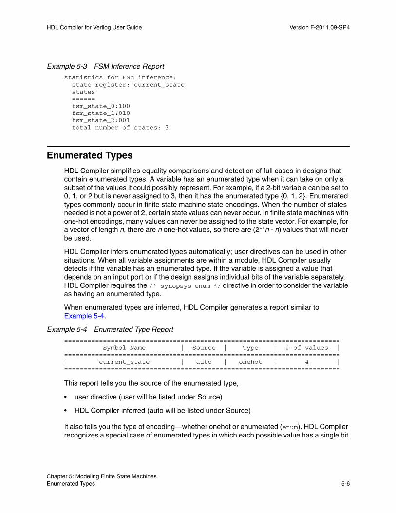
HDL Compiler for Verilog User Guide F-2011.09-SP4HDL Compiler for Verilog User Guide Version F-2011.09-SP4
Example 5-3 FSM Inference Report
statistics for FSM inference: state register: current_state states ====== fsm_state_0:100 fsm_state_1:010 fsm_state_2:001 total number of states: 3
Enumerated Types
HDL Compiler simplifies equality comparisons and detection of full cases in designs that contain enumerated types. A variable has an enumerated type when it can take on only a subset of the values it could possibly represent. For example, if a 2-bit variable can be set to 0, 1, or 2 but is never assigned to 3, then it has the enumerated type {0, 1, 2}. Enumerated types commonly occur in finite state machine state encodings. When the number of states needed is not a power of 2, certain state values can never occur. In finite state machines with one-hot encodings, many values can never be assigned to the state vector. For example, for a vector of length n, there are n one-hot values, so there are (2**n - n) values that will never be used.
HDL Compiler infers enumerated types automatically; user directives can be used in other situations. When all variable assignments are within a module, HDL Compiler usually detects if the variable has an enumerated type. If the variable is assigned a value that depends on an input port or if the design assigns individual bits of the variable separately, HDL Compiler requires the /* synopsys enum */ directive in order to consider the variable as having an enumerated type.
When enumerated types are inferred, HDL Compiler generates a report similar to Example 5-4.
Example 5-4 Enumerated Type Report
=======================================================================| Symbol Name | Source | Type | # of values |=======================================================================| current_state | auto | onehot | 4 |=======================================================================
This report tells you the source of the enumerated type,
• user directive (user will be listed under Source)
• HDL Compiler inferred (auto will be listed under Source)
It also tells you the type of encoding—whether onehot or enumerated (enum). HDL Compiler recognizes a special case of enumerated types in which each possible value has a single bit
Chapter 5: Modeling Finite State Machines Enumerated Types 5-6
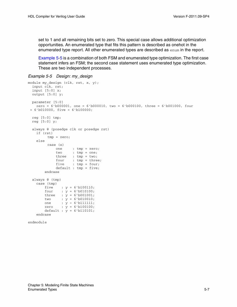
HDL Compiler for Verilog User Guide Version F-2011.09-SP4
set to 1 and all remaining bits set to zero. This special case allows additional optimization opportunities. An enumerated type that fits this pattern is described as onehot in the enumerated type report. All other enumerated types are described as enum in the report.
Example 5-5 is a combination of both FSM and enumerated type optimization. The first case statement infers an FSM; the second case statement uses enumerated type optimization. These are two independent processes.
Example 5-5 Design: my_designmodule my_design (clk, rst, x, y); input clk, rst; input [5:0] x; output [5:0] y;
parameter [5:0] zero = 6'b000001, one = 6'b000010, two = 6'b000100, three = 6'b001000, four = 6'b010000, five = 6'b100000;
reg [5:0] tmp; reg [5:0] y;
always @ (posedge clk or posedge rst) if (rst)
tmp = zero; else
case (x) one : tmp = zero; two : tmp = one; three : tmp = two; four : tmp = three; five : tmp = four; default : tmp = five;
endcase
always @ (tmp) case (tmp) five : y = 6'b100110; four : y = 6'b010100; three : y = 6'b001001; two : y = 6'b010010; one : y = 6'b111111; zero : y = 6'b100100; default : y = 6'b110101; endcase
endmodule
Chapter 5: Modeling Finite State Machines Enumerated Types 5-7Chapter 5: Modeling Finite State Machines Enumerated Types 5-7
HDL Compiler for Verilog User Guide F-2011.09-SP4HDL Compiler for Verilog User Guide Version F-2011.09-SP4
Chapter 5: Modeling Finite State Machines Enumerated Types 5-8
6Modeling Three-State Buffers 6
HDL Compiler infers a three-state driver when you assign the value z (high impedance) to a variable. HDL Compiler infers 1 three-state driver per variable per always block. You can assign high-impedance values to single-bit or bused variables. A three-state driver is represented as a TSGEN cell in the generic netlist. Three-state driver inference and instantiation are described in the following sections:
• Using z Values
• Three-State Driver Inference Report
• Assigning a Single Three-State Driver to a Single Variable
• Assigning Multiple Three-State Drivers to a Single Variable
• Registering Three-State Driver Data
• Instantiating Three-State Drivers
• Errors and Warnings
6-1
HDL Compiler for Verilog User Guide F-2011.09-SP4HDL Compiler for Verilog User Guide Version F-2011.09-SP4
Using z Values
You can use the z value in the following ways:
• Variable assignment
• Function call argument
• Return value
You can use the z value only in a comparison expression, such as in
if (IN_VAL == 1'bz) y=0;
This statement is permissible because IN_VAL == 1'bz is a comparison. However, it always evaluates to false, so it is also a simulation/synthesis mismatch. See “Comparisons to x or z Values” on page 2-25.
This code,
OUT_VAL = (1'bz && IN_VAL);
is not a comparison expression. HDL Compiler generates an error for this expression.
Three-State Driver Inference Report
The hdlin_reporting_level variable determines whether HDL Compiler generates a three-state inference report. If you do not want inference reports, set hdlin_reporting_level to none. The default is basic, meaning that a report will be generated. Example 6-1 shows a three-state inference report:
Example 6-1 Three-State Inference Report
=================================================| Register Name | Type | Width | MB |=================================================| T_tri | Tri-State Buffer | 1 | N |=================================================
The first column of the report indicates the name of the inferred three-state device. The second column indicates the type of inferred device. The third column indicates the width of the inferred device. The fourth column indicates whether the device is multibit. HDL Compiler generates the same report for the default and verbose reports for three-state inference. For more information about the hdlin_reporting_level variable, see “Elaboration Reports” on page 1-7.
Chapter 6: Modeling Three-State Buffers Using z Values 6-2

HDL Compiler for Verilog User Guide Version F-2011.09-SP4
Assigning a Single Three-State Driver to a Single Variable
Example 6-2 infers a single three-state driver and shows the associated inference report.
Example 6-2 Single Three-State Driver
module three_state (ENABLE, IN1, OUT1); input IN1, ENABLE; output OUT1; reg OUT1;always @(ENABLE or IN1) begin if (ENABLE) OUT1 = IN1; else OUT1 = 1'bz; //assigns high-impedance stateendendmodule
Inference Report=================================================| Register Name | Type | Width | MB |=================================================| OUT1_tri | Tri-State Buffer | 1 | N |=================================================
Example 6-3 infers a single three-state driver with MUXed inputs and shows the associated inference report.
Example 6-3 Single Three-State Driver With MUXed Inputs
module three_state (A, B, SELA, SELB, T); input A, B, SELA, SELB; output T; reg T; always @(SELA or SELB or A or B) begin T = 1'bz; if (SELA) T = A; if (SELB) T = B; endendmodule
Inference Report=================================================| Register Name | Type | Width | MB |=================================================| T_tri | Tri-State Buffer | 1 | N |=================================================
Chapter 6: Modeling Three-State Buffers Assigning a Single Three-State Driver to a Single Variable 6-3Chapter 6: Modeling Three-State Buffers Assigning a Single Three-State Driver to a Single Variable 6-3

HDL Compiler for Verilog User Guide F-2011.09-SP4HDL Compiler for Verilog User Guide Version F-2011.09-SP4
Assigning Multiple Three-State Drivers to a Single Variable
When assigning multiple three-state drivers to a single variable, as shown in Figure 6-1, always use assign statements, as shown in Example 6-4.
Figure 6-1 Two Three-State Drivers Assigned to a Single Variable
T
SELB
B
SELA
A
Example 6-4 Correct Method
module three_state (A, B, SELA, SELB, T); input A, B, SELA, SELB; output T; assign T = (SELA) ? A : 1'bz; assign T = (SELB) ? B : 1'bz;endmodule
Do not use multiple always blocks (shown in Example 6-5). Multiple always blocks cause a simulation/synthesis mismatch because the reg data type is not resolved. Note that the tool does not display a warning for this mismatch.
Example 6-5 Incorrect Method
module three_state (A, B, SELA, SELB, T); input A, B, SELA, SELB; output T; reg T; always @(SELA or A) if (SELA) T = A; else T = 1'bz; always @(SELB or B) if (SELB) T = B; else T = 1'bz;endmodule
Chapter 6: Modeling Three-State Buffers Assigning Multiple Three-State Drivers to a Single Variable 6-4

HDL Compiler for Verilog User Guide Version F-2011.09-SP4
Registering Three-State Driver Data
When a variable is registered in the same block in which it is defined as a three-state driver, HDL Compiler also registers the driver’s enable signal, as shown in Example 6-6. Figure 6-2 shows the compiled gates and the associated inference report.
Example 6-6 Three-State Driver With Enable and Data Registeredmodule ff_3state (DATA, CLK, THREE_STATE, OUT1); input DATA, CLK, THREE_STATE; output OUT1; reg OUT1;always @ (posedge CLK) begin if (THREE_STATE) OUT1 = 1'bz; else OUT1 = DATA;endendmodule
Inference reports:
=============================================================================|Register Name | Type | Width | Bus | MB | AR | AS | SR | SS | ST |=============================================================================|OUT1_reg |Flip-flop | 1 | N | N | N | N | N | N | N ||OUT1_tri_enable_reg |Flip-flop | 1 | N | N | N | N | N | N | N |=============================================================================
=================================================| Register Name | Type | Width | MB |=================================================| OUT1_tri | Tri-State Buffer | 1 | N |=================================================
Figure 6-2 Three-State Driver With Enable and Data Registered
Chapter 6: Modeling Three-State Buffers Registering Three-State Driver Data 6-5Chapter 6: Modeling Three-State Buffers Registering Three-State Driver Data 6-5
HDL Compiler for Verilog User Guide F-2011.09-SP4HDL Compiler for Verilog User Guide Version F-2011.09-SP4
Instantiating Three-State Drivers
The following gate types are supported:
• bufif0 (active-low enable line)
• bufif1 (active-high enable line)
• notif0 (active-low enable line, output inverted)
• notif1 (active-high enable line, output inverted)
Connection lists for bufif and notif gates use positional notation. Specify the order of the terminals as follows:
• The first terminal connects to the output of the gate.
• The second terminal connects to the input of the gate.
• The third terminal connects to the control line.
Example 6-7 shows a three-state gate instantiation with an active-high enable and no inverted output.
Example 6-7 Three-State Gate Instantiation
module three_state (in1,out1,cntrl1);input in1,cntrl1;output out1;
bufif1 (out1,in1,cntrl1);endmodule
Errors and Warnings
When you use the coding styles recommended in this chapter, you do not need to declare variables that drive multiply driven nets as tri data objects. But if you don’t use these coding styles, or you don’t declare the variable as a tri data object, HDL Compiler issues an ELAB-366 error message and terminates. To force HDL Compiler to warn for this condition (ELAB-365) but continue to create a netlist, set hdlin_prohibit_nontri_multiple_drivers to false (the default is true). With this variable false, HDL Compiler builds the generic netlist for all legal designs. If a design is illegal, such as when one of the drivers is a constant, HDL Compiler issues an error.
Chapter 6: Modeling Three-State Buffers Instantiating Three-State Drivers 6-6

HDL Compiler for Verilog User Guide Version F-2011.09-SP4
The following code generates an ELAB-366 error message (OUT1 is a reg being driven by two always@ blocks):
module three_state (ENABLE, IN1, RESET, OUT1);
input IN1, ENABLE, RESET; output OUT1; reg OUT1;
always @(IN1 or ENABLE) if (ENABLE) OUT1 = IN1;
always@ (RESET) if (RESET) OUT1 = 1'b0;endmodule
The ELAB-366 error message is
Error: Net '/...v:14: OUT1' or a directly connected net is driven by more than one source, and not all drivers are three-state. (ELAB-366)
Chapter 6: Modeling Three-State Buffers Errors and Warnings 6-7Chapter 6: Modeling Three-State Buffers Errors and Warnings 6-7
HDL Compiler for Verilog User Guide F-2011.09-SP4HDL Compiler for Verilog User Guide Version F-2011.09-SP4
Chapter 6: Modeling Three-State Buffers Errors and Warnings 6-8

7HDL Compiler Synthesis Directives 7
HDL Compiler synthesis directives are special comments that affect the actions of HDL Compiler and Design Compiler. These comments are ignored by other tools. HDL Compiler synthesis directives begin with //synopsys or /*synopsys. The //$s or //$S notation can be used as a shortcut for //synopsys. The simulator ignores these directives. The syntax descriptions in this chapter primarily show the //synopsys notation.
Note: HDL Compiler reports a syntax error if you use //synopsys in a regular comment.
The following sections describe the HDL Compiler synthesis directives:
• async_set_reset
• async_set_reset_local
• async_set_reset_local_all
• dc_tcl_script_begin and dc_tcl_script_end
• enum
• full_case
• infer_multibit and dont_infer_multibit
• infer_mux
• infer_onehot_mux
7-1

HDL Compiler for Verilog User Guide F-2011.09-SP4HDL Compiler for Verilog User Guide Version F-2011.09-SP4
• keep_signal_name
• one_cold
• one_hot
• parallel_case
• preserve_sequential
• sync_set_reset
• sync_set_reset_local
• sync_set_reset_local_all
• template
• translate_off and translate_on (Deprecated)
Chapter 7: HDL Compiler Synthesis Directives 7-2

HDL Compiler for Verilog User Guide Version F-2011.09-SP4
async_set_reset
When you set the async_set_reset directive on a single-bit signal, HDL Compiler searches for a branch that uses the signal as a condition and then checks whether the branch contains an assignment to a constant value. If the branch does, the signal becomes an asynchronous reset or set. Use this directive on single-bit signals.
The syntax is
// synopsys async_set_reset "signal_name_list"
See Example A-20 on page A-31, Example A-22 on page A-31, and Example 4-20 on page 4-15.
async_set_reset_local
When you set the async_set_reset_local directive, HDL Compiler treats listed signals in the specified block as if they have the async_set_reset directive set.
Attach the async_set_reset_local directive to a block label using the following syntax:
// synopsys async_set_reset_local block_label "signal_name_list"
async_set_reset_local_all
When you set the async_set_reset_local_all directive, HDL Compiler treats all listed signals in the specified blocks as if they have the async_set_reset directive set. Attach the async_set_reset_local_all directive to a block label using the following syntax:
// synopsys async_set_reset_local_all "block_label_list"
To enable the async_set_reset_local_all behavior, you must set hdlin_ff_always_async_set_reset to false and use the coding style shown in Example 7-1.
Example 7-1 Coding Style
// To enable the async_set_reset_local_all behavior, you must set// hdlin_ff_always_async_set_reset to false in addition to coding per the below template.
module m1 (input rst,set,d,d1,clk,clk1, output reg q,q1);
// synopsys async_set_reset_local_all "sync_rst" always @(posedge clk or posedge rst or posedge set) begin :sync_rst if (rst) q <= 1'b0;
Chapter 7: HDL Compiler Synthesis Directives async_set_reset 7-3Chapter 7: HDL Compiler Synthesis Directives async_set_reset 7-3
HDL Compiler for Verilog User Guide F-2011.09-SP4HDL Compiler for Verilog User Guide Version F-2011.09-SP4
else if (set) q <= 1'b1; else q <= d;end
always @(posedge clk1 or posedge rst or posedge set) begin : default_rst if (rst) q1 <= 1'b0; else if (set) q1 <= 1'b1; else q1 <= d1;end
endmodule
dc_tcl_script_begin and dc_tcl_script_end
You can embed Tcl commands that set design constraints and attributes within the RTL by using the dc_tcl_script_begin and dc_tcl_script_end directives, as shown in Example 7-2 and Example 7-3.
Example 7-2 Embedding Constraints With // Delimiters
... // synopsys dc_tcl_script_begin// set_max_area 0.0// set_max_delay 0.0 port_z// synopsys dc_tcl_script_end...
Example 7-3 Embedding Constraints With /* and */ Delimiters
/* synopsys dc_tcl_script_begin set_max_area 10.0 set_max_delay 5.0 port_z*/
Design Compiler interprets the statements embedded between the dc_tcl_script_begin and the dc_tcl_script_end directives. If you want to comment out part of your script, use the # comment character.
The following items are not supported in embedded Tcl scripts:
• Hierarchical constraints
• Wildcards
• List commands
Chapter 7: HDL Compiler Synthesis Directives dc_tcl_script_begin and dc_tcl_script_end 7-4
HDL Compiler for Verilog User Guide Version F-2011.09-SP4
• Multiple line commands
Observe the following guidelines when using embedded Tcl scripts:
• Constraints and attributes declared outside a module apply to all subsequent modules declared in the file.
• Constraints and attributes declared inside a module apply only to the enclosing module.
• Any dc_shell scripts embedded in functions apply to the whole module.
• Include only commands that set constraints and attributes. Do not use action commands such as compile, gen, and report. The tool ignores these commands and issues a warning or error message.
• The constraints or attributes set in the embedded script go into effect after the read command is executed. Therefore, variables that affect the read process itself are not in effect before the read.
• Error checking is done after the read command finishes. Syntactic and semantic errors in dc_shell strings are reported at this time.
• You can have more than one dc_tcl_script_begin / dc_tcl_script_end pair per file or module. The compiler does not issue an error or warning when it sees more than one pair. Each pair is evaluated and set on the applicable code.
• An embedded dc_shell script does not produce any information or status messages unless there is an error in the script.
• If you use embedded Tcl scripts while running in dcsh mode, Design Compiler issues the following error message:
Error: Design 'MID' has embedded Tcl commands which are ignored in EQN mode. (UIO-162)
• Usage of built-in Tcl commands is not recommended.
• Usage of output redirection commands is not recommended.
enum
Use the enum directive with the Verilog parameter definition statement to specify state machine encodings.
The syntax of the enum directive is
// synopsys enum enum_name
Example 7-4 shows the declaration of an enumeration of type colors that is 3 bits wide and has the enumeration literals red, green, blue, and cyan with the values shown.
Chapter 7: HDL Compiler Synthesis Directives enum 7-5Chapter 7: HDL Compiler Synthesis Directives enum 7-5

HDL Compiler for Verilog User Guide F-2011.09-SP4HDL Compiler for Verilog User Guide Version F-2011.09-SP4
Example 7-4 Enumeration of Type Colors
parameter [2:0] // synopsys enum colorsred = 3'b000, green = 3'b001, blue = 3'b010, cyan = 3'b011;
The enumeration must include a size (bit-width) specification. Example 7-5 shows an invalid enum declaration.
Example 7-5 Invalid enum Declaration
parameter /* synopsys enum colors */ red = 3'b000, green = 1;// [2:0] required
Example 7-6 shows a register, a wire, and an input port with the declared type of colors. In each of the following declarations, the array bounds must match those of the enumeration declaration. If you use different bounds, synthesis might not agree with simulation behavior.
Example 7-6 enum Type Declarations
reg [2:0] /* synopsys enum colors */ counter;wire [2:0] /* synopsys enum colors */ peri_bus;input [2:0] /* synopsys enum colors */ input_port;
Even though you declare a variable to be of type enum, it can still be assigned a bit value that is not one of the enumeration values in the definition. Example 7-7 relates to Example 7-6 and shows an invalid encoding for colors.
Example 7-7 Invalid Bit Value Encoding for Colors
counter = 3'b111;
Because 111 is not in the definition for colors, it is not a valid encoding. HDL Compiler accepts this encoding, but issues a warning for this assignment.
You can use enumeration literals just like constants, as shown in Example 7-8.
Example 7-8 Enumeration Literals Used as Constants
if (input_port == blue) counter = red;
If you declare a port as a reg and as an enumerated type, you must declare the enumeration when you declare the port. Example 7-9 shows the declaration of the enumeration.
Chapter 7: HDL Compiler Synthesis Directives enum 7-6
HDL Compiler for Verilog User Guide Version F-2011.09-SP4
Example 7-9 Enumerated Type Declaration for a Port
module good_example (a,b);
parameter [1:0] /* synopsys enum colors */green = 2'b00, white = 2'b11;
input a; output [1:0] /* synopsys enum colors */ b; reg [1:0] b;..endmodule
Example 7-10 declares a port as an enumerated type incorrectly because the enumerated type declaration appears with the reg declaration instead of with the output declaration.
Example 7-10 Incorrect Enumerated Type Declaration for a Port
module bad_example (a,b);
parameter [1:0] /* synopsys enum colors */green = 2'b00, white = 2'b11;
input a; output [1:0] b; reg [1:0] /* synopsys enum colors */ b;..endmodule
full_case
This directive prevents HDL Compiler from generating logic to test for any value that is not covered by the case branches and creating an implicit default branch. Set the full_case directive on a case statement when you know that all possible branches of the case statement are listed within the case statement. When a variable is assigned in a case statement that is not full, the variable is conditionally assigned and requires a latch.
Warning: Marking a case statement as full when it actually is not full can cause the simulation to behave differently from the logic HDL Compiler synthesizes because HDL Compiler does not generate a latch to handle the implicit default condition.
The syntax for the full_case directive is
// synopsys full_case
Chapter 7: HDL Compiler Synthesis Directives full_case 7-7Chapter 7: HDL Compiler Synthesis Directives full_case 7-7
HDL Compiler for Verilog User Guide F-2011.09-SP4HDL Compiler for Verilog User Guide Version F-2011.09-SP4
In Example 7-11, full_case is set on the first case statement and parallel_case and full_case directives are set on the second case statement.
Example 7-11 // synopsys full_case Directives
module test (in, out, current_state, next_state); input [1:0] in; output reg [1:0] out; input [3:0] current_state; output reg [3:0] next_state;
parameter state1 = 4'b0001, state2 = 4'b0010,state3 = 4'b0100, state4 = 4'b1000;always @* begincase (in) // synopsys full_case0: out = 2;1: out = 3;2: out = 0;endcasecase (1) // synopsys parallel_case full_casecurrent_state[0] : next_state = state2;current_state[1] : next_state = state3;current_state[2] : next_state = state4;current_state[3] : next_state = state1;endcaseendendmodule
In the first case statement, the condition in == 3 is not covered. However, the designer knows that in == 3 will never occur and therefore sets the full_case directive on the case statement.
In the second case statement, not all 16 possible branch conditions are covered; for example, current_state == 4’b0101 is not covered. However,
• The designer knows that these states will never occur and therefore sets the full_case directive on the case statement.
• The designer also knows that only one branch is true at a time and therefore sets the parallel_case directive on the case statement.
In the following example, at least one branch will be taken because all possible values of sel are covered, that is, 00, 01, 10, and 11:
Chapter 7: HDL Compiler Synthesis Directives full_case 7-8
HDL Compiler for Verilog User Guide Version F-2011.09-SP4
module mux(a, b,c,d,sel,y); input a,b,c,d; input [1:0] sel; output y; reg y; always @ (a or b or c or d or sel) begin case (sel) 2'b00 : y=a; 2'b01 : y=b; 2'b10 : y=c; 2'b11 : y=d; endcase endendmodule
In the following example, the case statement is not full:
module mux(a, b,c,d,sel,y); input a,b,c,d; input [1:0] sel; output y; reg y; always @ (a or b or c or d or sel) begin case (sel) 2'b00 : y=a; 2'b11 : y=d; endcase endendmodule
It is unknown what happens when sel equals 01 and 10. In this case, HDL Compiler generates logic to test for any value that is not covered by the case branches and creates an implicit “default” branch that contains no actions. When a variable is assigned in a case statement that is not full, the variable is conditionally assigned and requires a latch.
infer_multibit and dont_infer_multibit
You can infer registers, multiplexers, and three-state cells that have identical structures as multibit components.
The following sections describe how to use the multibit inference directives:
• Using the infer_multibit Directive
• Using the dont_infer_multibit Directive
• Reporting Multibit Components
Chapter 7: HDL Compiler Synthesis Directives infer_multibit and dont_infer_multibit 7-9Chapter 7: HDL Compiler Synthesis Directives infer_multibit and dont_infer_multibit 7-9
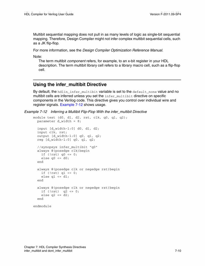
HDL Compiler for Verilog User Guide F-2011.09-SP4HDL Compiler for Verilog User Guide Version F-2011.09-SP4
Multibit sequential mapping does not pull in as many levels of logic as single-bit sequential mapping. Therefore, Design Compiler might not infer complex multibit sequential cells, such as a JK flip-flop.
For more information, see the Design Compiler Optimization Reference Manual.
Note: The term multibit component refers, for example, to an x-bit register in your HDL description. The term multibit library cell refers to a library macro cell, such as a flip-flop cell.
Using the infer_multibit DirectiveBy default, the hdlin_infer_multibit variable is set to the default_none value and no multibit cells are inferred unless you set the infer_multibit directive on specific components in the Verilog code. This directive gives you control over individual wire and register signals. Example 7-12 shows usage.
Example 7-12 Inferring a Multibit Flip-Flop With the infer_multibit Directive
module test (d0, d1, d2, rst, clk, q0, q1, q2); parameter d_width = 8;
input [d_width-1:0] d0, d1, d2; input clk, rst; output [d_width-1:0] q0, q1, q2; reg [d_width-1:0] q0, q1, q2;
//synopsys infer_multibit "q0" always @(posedge clk)begin if (!rst) q0 <= 0; else q0 <= d0; end
always @(posedge clk or negedge rst)begin if (!rst) q1 <= 0; else q1 <= d1; end
always @(posedge clk or negedge rst)begin if (!rst) q2 <= 0; else q2 <= d2; end
endmodule
Chapter 7: HDL Compiler Synthesis Directives infer_multibit and dont_infer_multibit 7-10
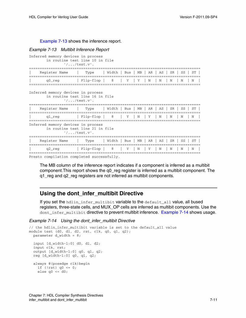
HDL Compiler for Verilog User Guide Version F-2011.09-SP4
Example 7-13 shows the inference report.
Example 7-13 Multibit Inference ReportInferred memory devices in process in routine test line 10 in file '/.../test.v'.===============================================================================| Register Name | Type | Width | Bus | MB | AR | AS | SR | SS | ST |===============================================================================| q0_reg | Flip-flop | 8 | Y | Y | N | N | N | N | N |===============================================================================
Inferred memory devices in process in routine test line 16 in file '/.../test.v'.===============================================================================| Register Name | Type | Width | Bus | MB | AR | AS | SR | SS | ST |===============================================================================| q1_reg | Flip-flop | 8 | Y | N | Y | N | N | N | N |===============================================================================Inferred memory devices in process in routine test line 21 in file '/.../test.v'.===============================================================================| Register Name | Type | Width | Bus | MB | AR | AS | SR | SS | ST |===============================================================================| q2_reg | Flip-flop | 8 | Y | N | Y | N | N | N | N |===============================================================================Presto compilation completed successfully.
The MB column of the inference report indicates if a component is inferred as a multibit component.This report shows the q0_reg register is inferred as a multibit component. The q1_reg and q2_reg registers are not inferred as multibit components.
Using the dont_infer_multibit DirectiveIf you set the hdlin_infer_multibit variable to the default_all value, all bused registers, three-state cells, and MUX_OP cells are inferred as multibit components. Use the dont_infer_multibit directive to prevent multibit inference. Example 7-14 shows usage.
Example 7-14 Using the dont_infer_multibit Directive// the hdlin_infer_multibit variable is set to the default_all valuemodule test (d0, d1, d2, rst, clk, q0, q1, q2); parameter d_width = 8;
input [d_width-1:0] d0, d1, d2; input clk, rst; output [d_width-1:0] q0, q1, q2; reg [d_width-1:0] q0, q1, q2;
always @(posedge clk)begin if (!rst) q0 <= 0; else q0 <= d0;
Chapter 7: HDL Compiler Synthesis Directives infer_multibit and dont_infer_multibit 7-11Chapter 7: HDL Compiler Synthesis Directives infer_multibit and dont_infer_multibit 7-11
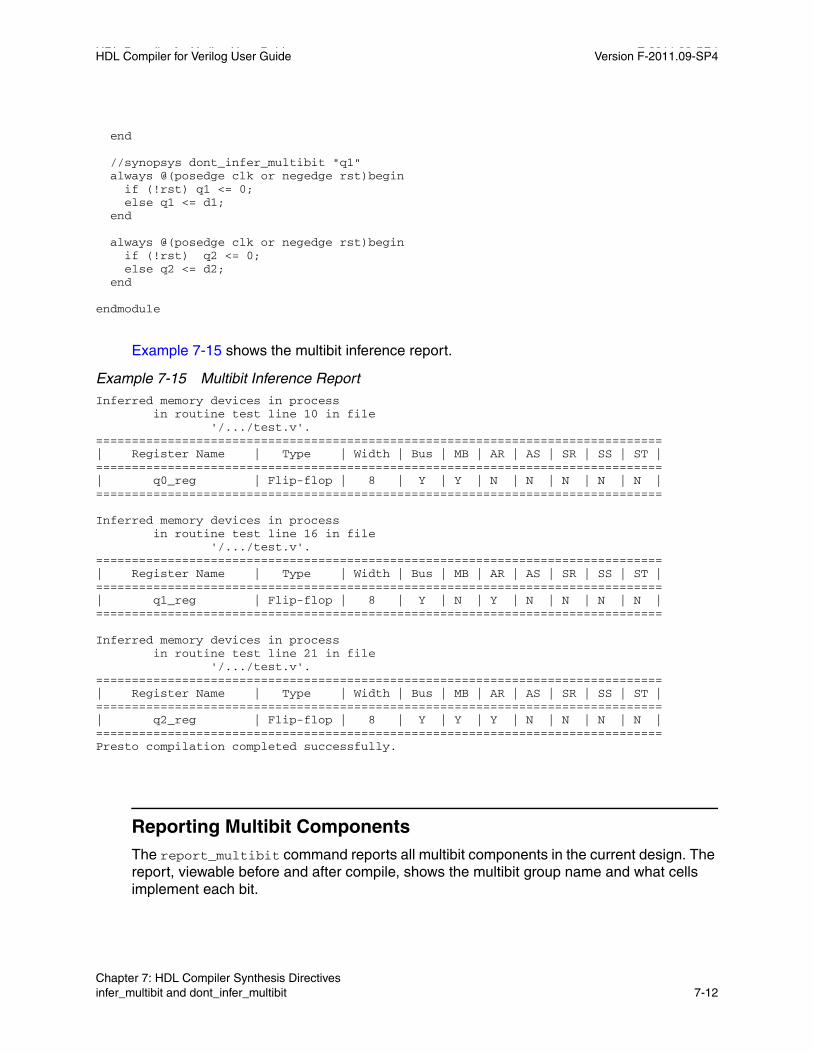
HDL Compiler for Verilog User Guide F-2011.09-SP4HDL Compiler for Verilog User Guide Version F-2011.09-SP4
end
//synopsys dont_infer_multibit "q1" always @(posedge clk or negedge rst)begin if (!rst) q1 <= 0; else q1 <= d1; end
always @(posedge clk or negedge rst)begin if (!rst) q2 <= 0; else q2 <= d2; end
endmodule
Example 7-15 shows the multibit inference report.
Example 7-15 Multibit Inference ReportInferred memory devices in process in routine test line 10 in file '/.../test.v'.===============================================================================| Register Name | Type | Width | Bus | MB | AR | AS | SR | SS | ST |===============================================================================| q0_reg | Flip-flop | 8 | Y | Y | N | N | N | N | N |===============================================================================
Inferred memory devices in process in routine test line 16 in file '/.../test.v'.===============================================================================| Register Name | Type | Width | Bus | MB | AR | AS | SR | SS | ST |===============================================================================| q1_reg | Flip-flop | 8 | Y | N | Y | N | N | N | N |===============================================================================
Inferred memory devices in process in routine test line 21 in file '/.../test.v'.===============================================================================| Register Name | Type | Width | Bus | MB | AR | AS | SR | SS | ST |===============================================================================| q2_reg | Flip-flop | 8 | Y | Y | Y | N | N | N | N |===============================================================================Presto compilation completed successfully.
Reporting Multibit Components The report_multibit command reports all multibit components in the current design. The report, viewable before and after compile, shows the multibit group name and what cells implement each bit.
Chapter 7: HDL Compiler Synthesis Directives infer_multibit and dont_infer_multibit 7-12
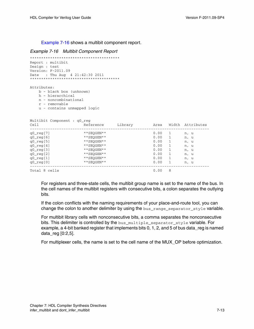
HDL Compiler for Verilog User Guide Version F-2011.09-SP4
Example 7-16 shows a multibit component report.
Example 7-16 Multibit Component Report****************************************Report : multibitDesign : testVersion: F-2011.09Date : Thu Aug 4 21:42:30 2011****************************************
Attributes: b - black box (unknown) h - hierarchical n - noncombinational r - removable u - contains unmapped logic
Multibit Component : q0_regCell Reference Library Area Width Attributes--------------------------------------------------------------------------------q0_reg[7] **SEQGEN** 0.00 1 n, uq0_reg[6] **SEQGEN** 0.00 1 n, uq0_reg[5] **SEQGEN** 0.00 1 n, uq0_reg[4] **SEQGEN** 0.00 1 n, uq0_reg[3] **SEQGEN** 0.00 1 n, uq0_reg[2] **SEQGEN** 0.00 1 n, uq0_reg[1] **SEQGEN** 0.00 1 n, uq0_reg[0] **SEQGEN** 0.00 1 n, u--------------------------------------------------------------------------------Total 8 cells 0.00 8
For registers and three-state cells, the multibit group name is set to the name of the bus. In the cell names of the multibit registers with consecutive bits, a colon separates the outlying bits.
If the colon conflicts with the naming requirements of your place-and-route tool, you can change the colon to another delimiter by using the bus_range_separator_style variable.
For multibit library cells with nonconsecutive bits, a comma separates the nonconsecutive bits. This delimiter is controlled by the bus_multiple_separator_style variable. For example, a 4-bit banked register that implements bits 0, 1, 2, and 5 of bus data_reg is named data_reg [0:2,5].
For multiplexer cells, the name is set to the cell name of the MUX_OP before optimization.
Chapter 7: HDL Compiler Synthesis Directives infer_multibit and dont_infer_multibit 7-13Chapter 7: HDL Compiler Synthesis Directives infer_multibit and dont_infer_multibit 7-13
HDL Compiler for Verilog User Guide F-2011.09-SP4HDL Compiler for Verilog User Guide Version F-2011.09-SP4
infer_mux
The infer_mux directive enables you to infer MUX_OP cells for a specific case or if statement, as shown:
always@(SEL) begincase (SEL) // synopsys infer_mux 2'b00: DOUT <= DIN[0]; 2'b01: DOUT <= DIN[1]; 2'b10: DOUT <= DIN[2]; 2'b11: DOUT <= DIN[3];endcase
You must use a simple variable as the control expression; for example, you can use the input "A" but not the negation of input "A". If statements have special coding considerations. For more information, see “MUX_OP Inference” on page 3-15 and “Considerations When Using If Statements to Code For MUX_OPs” on page 3-22.
infer_onehot_mux
The infer_onehot_mux directive enables you to map combinational logic to one-hot multiplexers in the technology library. For details, see “One-Hot Multiplexer Inference” on page 3-14.
keep_signal_name
Use the keep_signal_name directive to provide HDL Compiler with guidelines for preserving signal names.
The syntax is
// synopsys keep_signal_name "signal_name_list"
Set the keep_signal_name directive on a signal before any reference is made to that signal; for example, one methodology is to put the directive immediately after the declaration of the signal.
For examples, see “Keeping Signal Names” on page 2-19.
Chapter 7: HDL Compiler Synthesis Directives infer_mux 7-14

HDL Compiler for Verilog User Guide Version F-2011.09-SP4
one_cold
A one-cold implementation indicates that all signals in a group are active-low and that only one signal can be active at a given time. Synthesis implements the one_cold directive by omitting a priority circuit in front of the flip-flop. Simulation ignores the directive. The one_cold directive prevents Design Compiler from implementing priority-encoding logic for the set and reset signals. Attach this directive to set or reset signals on sequential devices, using the following syntax:
// synopsys one_cold signal_name_list
See Example 4-22 on page 4-16.
one_hot
A one-hot implementation indicates that all signals in a group are active-high and that only one signal can be active at a given time. Synthesis implements the one_hot directive by omitting a priority circuit in front of a flip-flop. Simulation ignores the directive. The one_hot directive prevents Design Compiler from implementing priority-encoding logic for the set and reset signals. Attach this directive to set or reset signals on sequential devices, using the following syntax:
// synopsys one_hot signal_name_list
See Example 4-30 on page 4-19 and Example A-32 on page A-36.
parallel_case
Set the parallel_case directive on a case statement when you know that only one branch of the case statement will be true at a time. This directive prevents HDL Compiler from building additional logic to ensure the first occurrence of a true branch is executed if more than one branch were true at one time.
Warning: Marking a case statement as parallel when it actually is not parallel can cause the simulation to behave differently from the logic HDL Compiler synthesizes because HDL Compiler does not generate priority encoding logic to make sure that the branch listed first in the case statement takes effect.
The syntax for the parallel_case directive is
// synopsys parallel_case
Use the parallel_case directive immediately after the case expression. In Example 7-17, the states of a state machine are encoded as a one-hot signal; the designer knows that only
Chapter 7: HDL Compiler Synthesis Directives one_cold 7-15Chapter 7: HDL Compiler Synthesis Directives one_cold 7-15
HDL Compiler for Verilog User Guide F-2011.09-SP4HDL Compiler for Verilog User Guide Version F-2011.09-SP4
one branch is true at a time and therefore sets the synopsys parallel_case directive on the case statement.
Example 7-17 parallel_case Directives
reg [3:0] current_state, next_state;parameter state1 = 4’b0001, state2 = 4’b0010,
state3 = 4’b0100, state4 = 4’b1000;case (1)//synopsys parallel_case current_state[0] : next_state = state2; current_state[1] : next_state = state3; current_state[2] : next_state = state4; current_state[3] : next_state = state1;endcase
When a case statement is not parallel (more than one branch evaluates to true), priority encoding is needed to ensure that the branch listed first in the case statement takes effect.
The following table summarizes the types of case statements.
Case statement description Additional logic
Full and parallel No additional logic is generated.
Full but not parallel Priority-encoded logic: HDL Compiler generates logic to ensure that the branch listed first in the case statement takes effect.
Parallel but not full Latches created: HDL Compiler generates logic to test for any value that is not covered by the case branches and creates an implicit “default” branch that requires a latch.
Not parallel and not full Priority-encoded logic: HDL Compiler generates logic to make sure that the branch listed first in the case statement takes effect.
Latches created: HDL Compiler generates logic to test for any value that is not covered by the case branches and creates an implicit “default” branch that requires a latch.
Chapter 7: HDL Compiler Synthesis Directives parallel_case 7-16
HDL Compiler for Verilog User Guide Version F-2011.09-SP4
preserve_sequential
The preserve_sequential directive allows you to preserve specific cells that would otherwise be optimized away by HDL Compiler. See “Keeping Unloaded Registers” on page 4-9.
sync_set_reset
Use the sync_set_reset directive to infer a D flip-flop with a synchronous set/reset. When you compile your design, the SEQGEN inferred by HDL Compiler will be mapped to a flip-flop in the technology library with a synchronous set/reset pin, or Design Compiler will use a regular D flip-flop and build synchronous set/reset logic in front of the D pin. The choice depends on which method provides a better optimization result.
It is important to use the sync_set_reset directive to label the set/reset signal because it tells Design Compiler that the signal should be kept as close to the register as possible during mapping, preventing a simulation/synthesis mismatch which can occur if the set/reset signal is masked by an X during initialization in simulation.
When a single-bit signal has this directive set to true, HDL Compiler checks the signal to determine whether it synchronously sets or resets a register in the design. Attach this directive to single-bit signals. Use the following syntax:
//synopsys sync_set_reset "signal_name_list"
For an example of a D flip-flop with a synchronous set signal that uses the sync_set_reset directive, see Example A-30 on page A-35. For an example of a JK flip-flop with synchronous set and reset signals that uses the sync_set_reset directive, see Example A-32 on page A-36.
For an example of a D flip-flop with a synchronous reset signal that uses the sync_set_reset directive, see Example 4-32 on page 4-20. For an example of multiple flip-flops with asynchronous and synchronous controls, see Example 4-36 on page 4-23.
sync_set_reset_local
The sync_set_reset_local directive instructs HDL Compiler to treat signals listed in a specified block as if they have the sync_set_reset directive set to true.
Attach this directive to a block label, using the following syntax:
//synopsys sync_set_reset_local block_label "signal_name_list"
Chapter 7: HDL Compiler Synthesis Directives preserve_sequential 7-17Chapter 7: HDL Compiler Synthesis Directives preserve_sequential 7-17

HDL Compiler for Verilog User Guide F-2011.09-SP4HDL Compiler for Verilog User Guide Version F-2011.09-SP4
Example 7-18 shows the usage.
Example 7-18 sync_set_reset_local Usage
module m1 (input d1,d2,clk, set1, set2, rst1, rst2, output reg q1,q2);
// synopsys sync_set_reset_local sync_rst "rst1"//always@(posedge clk or negedge rst1) always@(posedge clk ) begin: sync_rst if(~rst1) q1 = 1'b0; else if (set1) q1 = 1'b1; else q1 = d1; end
always@(posedge clk) begin: default_rst if(~rst2) q2 = 1'b0; else if (set2) q2 = 1'b1; else q2 = d2; end
endmodule
sync_set_reset_local_all
The sync_set_reset_local_all directive instructs HDL Compiler to treat all signals listed in the specified blocks as if they have the sync_set_reset directive set to true.
Attach this directive to a block label, using the following syntax:
// synopsys sync_set_reset_local_all "block_label_list"
Chapter 7: HDL Compiler Synthesis Directives sync_set_reset_local_all 7-18

HDL Compiler for Verilog User Guide Version F-2011.09-SP4
Example 7-19 shows usage.
Example 7-19 sync_set_reset_local_all Usage
module m2 (input d1,d2,clk, set1, set2, rst1, rst2, output reg q1,q2);
// synopsys sync_set_reset_local_all sync_rst//always@(posedge clk or negedge rst1) always@(posedge clk ) begin: sync_rst if(~rst1) q1 = 1'b0; else if (set1) q1 = 1'b1; else q1 = d1; end
always@(posedge clk) begin: default_rst if(~rst2) q2 = 1'b0; else if (set2) q2 = 1'b1; else q2 = d2; end
endmodule
template
The template directive saves an analyzed file and does not elaborate it. Without this directive, the analyzed file is saved and elaborated. If you use this directive and your design contains parameters, the design is saved as a template. Example 7-20 shows usage.
Example 7-20 template Directive
module template (a, b, c); input a, b, c; // synopsys template parameter width = 8;...endmodule
For more information, see “Parameterized Designs” on page 1-19.
Chapter 7: HDL Compiler Synthesis Directives template 7-19Chapter 7: HDL Compiler Synthesis Directives template 7-19

HDL Compiler for Verilog User Guide F-2011.09-SP4HDL Compiler for Verilog User Guide Version F-2011.09-SP4
translate_off and translate_on (Deprecated)
The translate_off and translate_on directives are deprecated. To suspend translation of the source code for synthesis, use the SYNTHESIS macro and the appropriate conditional directives (`ifdef, `ifndef, `else, `endif) rather than translate_off and translate_on.
The SYNTHESIS macro replaces the DC macro (DC is still supported for backward compatibility). See “Predefined Macros” on page 1-18.
Chapter 7: HDL Compiler Synthesis Directives translate_off and translate_on (Deprecated) 7-20
8HDL Compiler Variables 8
This chapter describes the Verilog reading and writing variables in the following sections:
• HDL Compiler Reading-Related Variables
• Commands for Writing Out Verilog
• Variables for Writing Out Verilog
8-1

HDL Compiler for Verilog User Guide F-2011.09-SP4HDL Compiler for Verilog User Guide Version F-2011.09-SP4
HDL Compiler Reading-Related Variables
Reading-related variables are described in Table 8-1. For more information about these variables, see the man pages.
Table 8-1 Reading-Related Variables
Name Default Description
bus_inference_style "" Specifies the pattern used to infer individual bits into a port bus.
bus_naming_style {%s[%d]} Controls the naming of elements in an array.
hdlin_auto_save_templates false Controls whether designs containing parameters are read in as templates. See “Reading Verilog Designs” on page 1-3. When set to true, the automatic netlist reader is disabled.
hdlin_check_no_latch false Controls whether a warning message is issued if a latch is inferred from a design. See “Preventing Unwanted Latches: hdlin_check_no_latch” on page 4-12.
hdlin_elab_errors_deep false Allows the elaboration of submodules even if the top-level module elaboration fails, enabling HDL Compiler to report more elaboration, link, and VER-37 errors and warnings in a hierarchical design during the first elaboration run. See “Reporting Elaboration Errors” on page 1-9.
hdlin_ff_always_async_set_ reset
true When this variable is true, HDL Compiler attempts to infer asynchronous set and reset conditions for flip-flops.
hdlin_ff_always_sync_set_ reset
false When this variable is true, HDL Compiler attempts to infer synchronous set and reset conditions for flip-flops.
hdlin_infer_function_local_ latches
false Allows latches to be inferred for function- and task-scope variables. See “Persistence of Values Across Calls to Tasks” on page 2-17.
Chapter 8: HDL Compiler Variables HDL Compiler Reading-Related Variables 8-2

HDL Compiler for Verilog User Guide Version F-2011.09-SP4
hdlin_infer_multibit default _none
Controls multibit inference for signals that have the infer_multibit directive in the Verilog description.
Options:
• default_none (default)—Infers multibit components for signals that have the infer_multibit directive in the Verilog description.
• default_all—Infers multibit components for all bused registers, multiplexers, and three-state cells that are larger than 2 bits. If you want to implement as single-bit components all buses that are more than 4 bits, use set_multibit_options -minimum_width 4. This sets a minimum_multibit_width attribute on the design. (Use the dont_infer_multibit directive to disable multibit mapping for certain signals.)
• never—Does not infer multibit components, regardless of the attributes or directives in the HDL source.
See “Multibit Components” on page 2-19.
hdlin_infer_mux default Controls MUX_OP inference.
To infer a MUX_OP, the case statement must actually be parallel, or an error is reported.
Options:
• default—Infers MUX_OPs for parallel case and if statements that have the infer_mux directive attached.
• none—Does not infer MUX_OPs, regardless of the directives set in the RTL description. HDL Compiler generates a warning if hdlin_infer_mux = none and infer_mux are used in the RTL.
• all—Infers MUX_OPs for every parallel case and if statement in your design. This can negatively affect QoR, because it might be more efficient to implement the MUX_OPs as random logic instead of using a specialized multiplexer structure.
See “MUX_OP Inference” on page 3-15.
Table 8-1 Reading-Related Variables (Continued)
Name Default Description
Chapter 8: HDL Compiler Variables HDL Compiler Reading-Related Variables 8-3Chapter 8: HDL Compiler Variables HDL Compiler Reading-Related Variables 8-3

HDL Compiler for Verilog User Guide F-2011.09-SP4HDL Compiler for Verilog User Guide Version F-2011.09-SP4
hdlin_keep_signal_name all_ driving
Controls the preservation of nets and their respective net name.
Options:
• all—Tries to preserve all signal names.
• user—Tries to preserve a signal name only when you label it with the keep_signal_name directive.
• all_driving (default)—Tries to preserve all signal names that lead to outputs (no dangling nets).
• user_driving—Tries to preserve a signal name only when you label it with the keep_signal_name directive and it leads to an output (no dangling nets).
• none—Does not try to preserve any signal name; overrides and ignores the keep_signal_name directive.
See “Keeping Signal Names” on page 2-19.
hdlin_latch_always_async_ set_reset
false When this variable is true, HDL Compiler attempts to infer asynchronous set and reset conditions for latches. See “D Latch With Asynchronous Set and Reset: Use hdlin_latch_always_async_set_reset” on page 4-15.
hdlin_module_arch_name _splitting
true Splits Verilog module names into entity/architecture portions by two subsequent underscores.
hdlin_mux_oversize_ratio 100 Defined as the ratio of the number of MUX_OP inputs to the unique number of data inputs. When this ratio is exceeded, a MUX_OP will not be inferred and the circuit will be generated with SELECT_OPs. See “MUX_OP Inference” on page 3-15.
Table 8-1 Reading-Related Variables (Continued)
Name Default Description
Chapter 8: HDL Compiler Variables HDL Compiler Reading-Related Variables 8-4

HDL Compiler for Verilog User Guide Version F-2011.09-SP4
hdlin_mux_size_limit 32 Sets the maximum size of a MUX_OP that HDL Compiler can infer. If you set this variable to a value greater than 32, HDL Compiler may take an unusually long elaboration time.
If the number of branches in a case statement exceeds the maximum size specified by this variable, HDL Compiler generates the following message:
Warning: A mux was not inferred because case statement %s has a very large branching factor. (HDL-383)
See “MUX_OP Inference” on page 3-15.
hdlin_mux_size_min 2 Sets the minimum number of data inputs for a MUX_OP inference. See “MUX_OP Inference” on page 3-15.
Table 8-1 Reading-Related Variables (Continued)
Name Default Description
Chapter 8: HDL Compiler Variables HDL Compiler Reading-Related Variables 8-5Chapter 8: HDL Compiler Variables HDL Compiler Reading-Related Variables 8-5

HDL Compiler for Verilog User Guide F-2011.09-SP4HDL Compiler for Verilog User Guide Version F-2011.09-SP4
hdlin_preserve_sequential none Preserves unloaded sequential cells (latches or flip-flops) that would otherwise be removed during optimization by HDL Compiler. The following options are supported:
• none or false—No unloaded sequential cells are preserved. This is the default behavior.
• all or true—All unloaded sequential cells are preserved, excluding unloaded sequential cells that are used solely as loop variables.
• all+loop_variables or true+loop_variables—All unloaded sequential cells are preserved, including unloaded sequential cells that are used solely as loop variables.
• ff—Only flip-flop cells are preserved, excluding unloaded sequential cells that are used solely as loop variables.
• ff+loop_variables—Only flip-flop cells are preserved, including unloaded sequential cells that are used solely as loop variables.
• latch—Only unloaded latch cells are preserved, excluding unloaded sequential cells that are used solely as loop variables.
• latch+loop_variables—Only unloaded latch cells are preserved, including unloaded sequential cells that are used solely as loop variables.
Important: To preserve unloaded cells through compile, you must set compile_delete_unloaded_sequential_cells to false.
See “Keeping Unloaded Registers” on page 4-9.
hdlin_prohibit_nontri_ multiple_drivers
true Issues an error when a non-tri net is driven by more than one processes or continuous assignment.
hdlin_reporting_level false Enables and disables the finite state machine inference report. For details, see “FSM Inference Report” on page 5-5.
hdlin_subprogram_default_ values
false Reads tick-LEFT as default for variables instead of 0s.
Table 8-1 Reading-Related Variables (Continued)
Name Default Description
Chapter 8: HDL Compiler Variables HDL Compiler Reading-Related Variables 8-6
HDL Compiler for Verilog User Guide Version F-2011.09-SP4
Commands for Writing Out Verilog
Any design, regardless of initial format (equation, netlist, and so on), can be written out as a Verilog design using the commands change_names -rules verilog -hier and write -format verilog. The change_names command must be used before the write command.
Variables for Writing Out Verilog
The variables listed in Table 8-2 affect how designs are written out as Verilog files. To override the default settings, set these variables before you write out the design.
To list the current values of the variables that affect writing out Verilog, enter
list -variables hdl
For more information about writing out designs, see the Design Compiler documentation.
hdlin_upcase_names false Converts all Verilog names to uppercase.
hdlin_vrlg_std 2005 Specifies the Verilog standard to enforce: 1995, 2001, or 2005. See also “Controlling the Verilog Version Used for Reading RTL Files” on page 1-7 and “generate Statements” on page B-6.
Table 8-2 Verilogout Variables
Variable Description
verilogout_equation When this is set to true, Verilog assign statements (Boolean equations) are written out for combinational gates instead of for gate instantiations. Flip-flops and three-state cells are left instantiated. The default is false.
verilogout_higher_designs _first
When this is set to true, Verilog modules are ordered so that higher-level designs come before lower-level designs, as defined by the design hierarchy. The default is false.
Table 8-1 Reading-Related Variables (Continued)
Name Default Description
Chapter 8: HDL Compiler Variables Commands for Writing Out Verilog 8-7Chapter 8: HDL Compiler Variables Commands for Writing Out Verilog 8-7
HDL Compiler for Verilog User Guide F-2011.09-SP4HDL Compiler for Verilog User Guide Version F-2011.09-SP4
verilogout_no_tri When this is set to true, three-state nets are declared as Verilog wire instead of tri. This variable eliminates assign primitives and tran gates in your Verilog output, by connecting an output port directly to a component instantiation. The default is false.
verilogout_single_bit When this variable is set to true, vectored ports (or ports that use record types) are bit-blasted; if a port’s bit vector is N bits wide, it is written out to the Verilog file as N separate single-bit ports. When it is set to false, all ports are written out with their original data types. The default is false.
Table 8-2 Verilogout Variables (Continued)
Variable Description
Chapter 8: HDL Compiler Variables Variables for Writing Out Verilog 8-8
AExamples A
This appendix presents examples that demonstrate basic concepts of HDL Compiler. It also describes coding techniques for late-arriving signals and includes examples for SR latches, an asynchronously set D latch, master-slave latches, a D flip-flop with a synchronous set signal, and a JK flip-flop with synchronous set and reset signals. This appendix has the following sections:
• Count Zeros—Combinational Version
• Count Zeros—Sequential Version
• Drink Machine—State Machine Version
• Drink Machine—Count Nickels Version
• Carry-Lookahead Adder
• Coding for Late-Arriving Signals
• Instantiation of Arrays of Instances
• SR Latches
• D Latch With Asynchronous Set: Use async_set_reset
• Inferring Master-Slave Latches
• Inferring Flip-Flops
A-1
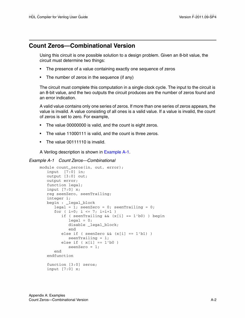
HDL Compiler for Verilog User Guide F-2011.09-SP4HDL Compiler for Verilog User Guide Version F-2011.09-SP4
Count Zeros—Combinational Version
Using this circuit is one possible solution to a design problem. Given an 8-bit value, the circuit must determine two things:
• The presence of a value containing exactly one sequence of zeros
• The number of zeros in the sequence (if any)
The circuit must complete this computation in a single clock cycle. The input to the circuit is an 8-bit value, and the two outputs the circuit produces are the number of zeros found and an error indication.
A valid value contains only one series of zeros. If more than one series of zeros appears, the value is invalid. A value consisting of all ones is a valid value. If a value is invalid, the count of zeros is set to zero. For example,
• The value 00000000 is valid, and the count is eight zeros.
• The value 11000111 is valid, and the count is three zeros.
• The value 00111110 is invalid.
A Verilog description is shown in Example A-1.
Example A-1 Count Zeros—Combinational
module count_zeros(in, out, error); input [7:0] in; output [3:0] out; output error; function legal; input [7:0] x; reg seenZero, seenTrailing; integer i; begin : _legal_block legal = 1; seenZero = 0; seenTrailing = 0; for ( i=0; i <= 7; i=i+1 ) if ( seenTrailing && (x[i] == 1'b0) ) begin legal = 0; disable _legal_block; end else if ( seenZero && (x[i] == 1'b1) ) seenTrailing = 1; else if ( x[i] == 1'b0 ) seenZero = 1; end endfunction
function [3:0] zeros; input [7:0] x;
Appendix A: Examples Count Zeros—Combinational Version A-2

HDL Compiler for Verilog User Guide Version F-2011.09-SP4
reg [3:0] count; integer i;
begin count = 0; for ( i=0; i <= 7; i=i+1 ) if ( x[i] == 1'b0 ) count = count + 1; zeros = count; end endfunction wire is_legal = legal(in); assign error = ! is_legal; assign out = is_legal ? zeros(in) : 1'b0;endmodule
This example shows two Verilog functions: legal and zeros. The function legal determines if the value is valid. It returns a 1-bit value: either 1 for a valid value or 0 for an invalid value. The function zeros cycles through all bits of the value, counts the number of zeros, and returns the appropriate value. The two functions are controlled by continuous assignment statements at the bottom of the module definition. This example shows a combinational (parallel) approach to counting zeros; the next example shows a sequential (serial) approach.
Count Zeros—Sequential Version
Example A-2 shows a sequential (clocked) solution to the “count zeros” design problem. The circuit specification is slightly different from the specification in the combinational solution and needs an initial reset signal to start the operation. The circuit now accepts the 8-bit string serially, 1 bit per clock cycle, using the data and clk inputs. The other two inputs are
• reset, which resets the circuit
• read, which causes the circuit to begin accepting data
The circuit’s three outputs are
• is_legal, which is true if the data is a valid value
• data_ready, which is true at the first invalid bit or when all 8 bits have been processed
• zeros, which is the number of zeros if is_legal is true
Example A-2 Count Zeros—Sequential Version
module count_zeros(data,reset,read,clk,zeros,is_legal, data_ready);
parameter TRUE=1, FALSE=0;
input data, reset, read, clk;
Chapter A: Examples Count Zeros—Sequential Version A-3Appendix A: Examples Count Zeros—Sequential Version A-3
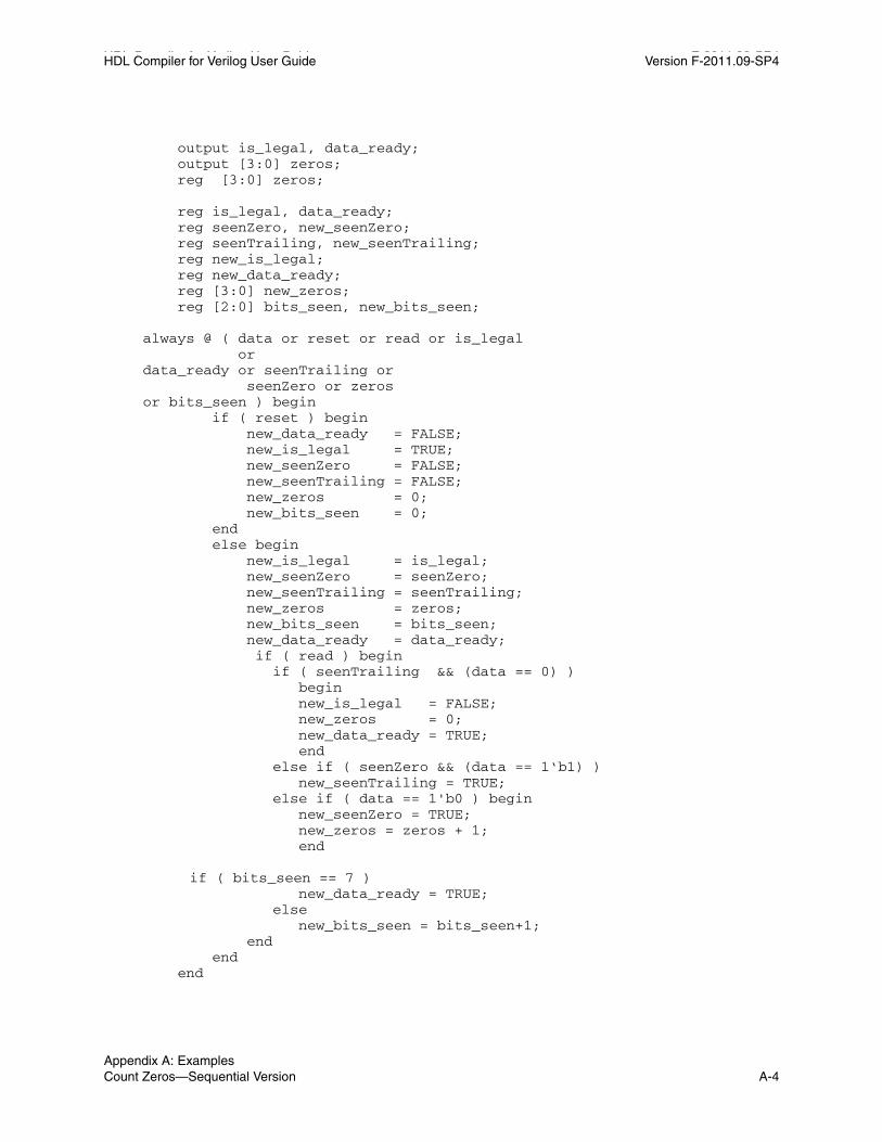
HDL Compiler for Verilog User Guide F-2011.09-SP4HDL Compiler for Verilog User Guide Version F-2011.09-SP4
output is_legal, data_ready; output [3:0] zeros; reg [3:0] zeros;
reg is_legal, data_ready; reg seenZero, new_seenZero; reg seenTrailing, new_seenTrailing; reg new_is_legal; reg new_data_ready; reg [3:0] new_zeros; reg [2:0] bits_seen, new_bits_seen;
always @ ( data or reset or read or is_legal or data_ready or seenTrailing or seenZero or zeros or bits_seen ) begin if ( reset ) begin new_data_ready = FALSE; new_is_legal = TRUE; new_seenZero = FALSE; new_seenTrailing = FALSE; new_zeros = 0; new_bits_seen = 0; end else begin new_is_legal = is_legal; new_seenZero = seenZero; new_seenTrailing = seenTrailing; new_zeros = zeros; new_bits_seen = bits_seen; new_data_ready = data_ready; if ( read ) begin if ( seenTrailing && (data == 0) ) begin new_is_legal = FALSE; new_zeros = 0; new_data_ready = TRUE; end else if ( seenZero && (data == 1‘b1) ) new_seenTrailing = TRUE; else if ( data == 1'b0 ) begin new_seenZero = TRUE; new_zeros = zeros + 1; end
if ( bits_seen == 7 ) new_data_ready = TRUE; else new_bits_seen = bits_seen+1; end end end
Appendix A: Examples Count Zeros—Sequential Version A-4

HDL Compiler for Verilog User Guide Version F-2011.09-SP4
always @ ( posedge clk) begin zeros = new_zeros; bits_seen = new_bits_seen; seenZero = new_seenZero; seenTrailing = new_seenTrailing; is_legal = new_is_legal; data_ready = new_data_ready;endendmodule
Drink Machine—State Machine Version
The next design is a vending control unit for a soft drink vending machine. The circuit reads signals from a coin input unit and sends outputs to a change dispensing unit and a drink dispensing unit.
Input signals from the coin input unit are nickel_in (nickel deposited), dime_in (dime deposited), and quarter_in (quarter deposited).
The price of a drink is 35 cents. The Verilog description for this design, shown in Example A-3, uses a state machine description style.
Chapter A: Examples Drink Machine—State Machine Version A-5Appendix A: Examples Drink Machine—State Machine Version A-5
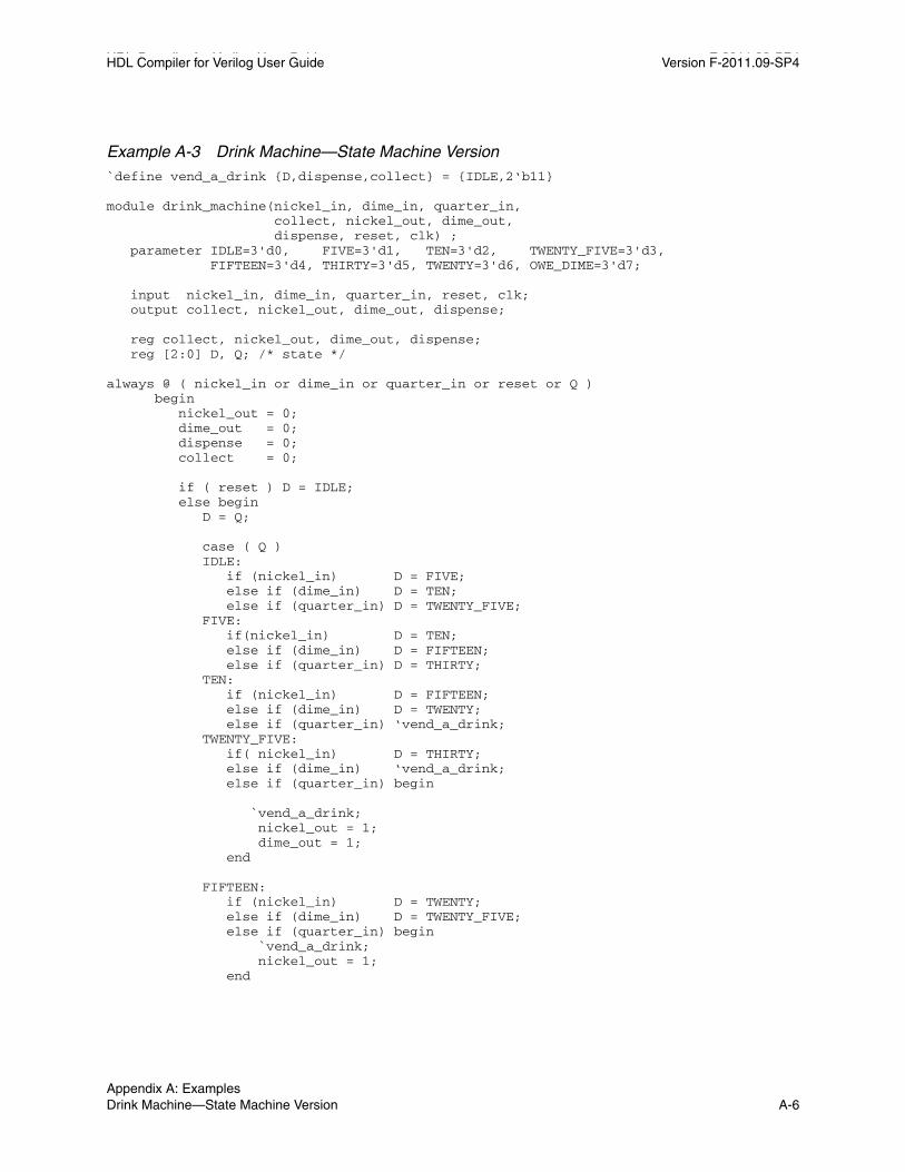
HDL Compiler for Verilog User Guide F-2011.09-SP4HDL Compiler for Verilog User Guide Version F-2011.09-SP4
Example A-3 Drink Machine—State Machine Version`define vend_a_drink {D,dispense,collect} = {IDLE,2‘b11}
module drink_machine(nickel_in, dime_in, quarter_in, collect, nickel_out, dime_out, dispense, reset, clk) ; parameter IDLE=3'd0, FIVE=3'd1, TEN=3'd2, TWENTY_FIVE=3'd3, FIFTEEN=3'd4, THIRTY=3'd5, TWENTY=3'd6, OWE_DIME=3'd7;
input nickel_in, dime_in, quarter_in, reset, clk; output collect, nickel_out, dime_out, dispense;
reg collect, nickel_out, dime_out, dispense; reg [2:0] D, Q; /* state */
always @ ( nickel_in or dime_in or quarter_in or reset or Q ) begin nickel_out = 0; dime_out = 0; dispense = 0; collect = 0;
if ( reset ) D = IDLE; else begin D = Q;
case ( Q ) IDLE: if (nickel_in) D = FIVE; else if (dime_in) D = TEN; else if (quarter_in) D = TWENTY_FIVE; FIVE: if(nickel_in) D = TEN; else if (dime_in) D = FIFTEEN; else if (quarter_in) D = THIRTY; TEN: if (nickel_in) D = FIFTEEN; else if (dime_in) D = TWENTY; else if (quarter_in) ‘vend_a_drink; TWENTY_FIVE: if( nickel_in) D = THIRTY; else if (dime_in) ‘vend_a_drink; else if (quarter_in) begin
`vend_a_drink; nickel_out = 1; dime_out = 1; end
FIFTEEN: if (nickel_in) D = TWENTY; else if (dime_in) D = TWENTY_FIVE; else if (quarter_in) begin `vend_a_drink; nickel_out = 1; end
Appendix A: Examples Drink Machine—State Machine Version A-6

HDL Compiler for Verilog User Guide Version F-2011.09-SP4
THIRTY: if (nickel_in) ‘vend_a_drink; else if (dime_in) begin `vend_a_drink; nickel_out = 1; end else if (quarter_in) begin `vend_a_drink; dime_out = 1; D = OWE_DIME; end
TWENTY: if (nickel_in) D = TWENTY_FIVE; else if (dime_in) D = THIRTY; else if (quarter_in) begin `vend_a_drink; dime_out = 1; end
OWE_DIME: begin dime_out = 1; D = IDLE; end endcase endend
always @ (posedge clk ) begin Q = D;endendmodule
Drink Machine—Count Nickels Version
Example A-4 uses the same design parameters as Example A-3, with the same input and output signals. In this version, a counter counts the number of nickels deposited. This counter is incremented by 1 if the deposit is a nickel, by 2 if it’s a dime, and by 5 if it is a quarter.
Chapter A: Examples Drink Machine—Count Nickels Version A-7Appendix A: Examples Drink Machine—Count Nickels Version A-7
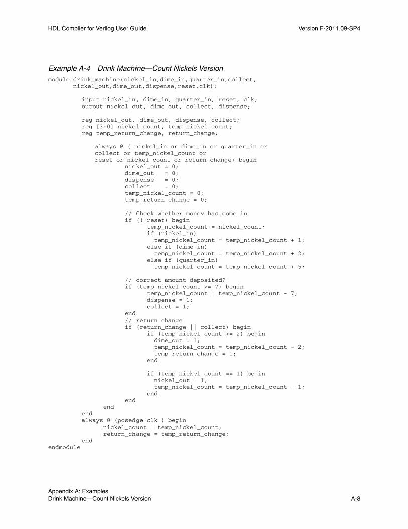
HDL Compiler for Verilog User Guide F-2011.09-SP4HDL Compiler for Verilog User Guide Version F-2011.09-SP4
Example A-4 Drink Machine—Count Nickels Versionmodule drink_machine(nickel_in,dime_in,quarter_in,collect, nickel_out,dime_out,dispense,reset,clk);
input nickel_in, dime_in, quarter_in, reset, clk;output nickel_out, dime_out, collect, dispense;
reg nickel_out, dime_out, dispense, collect;reg [3:0] nickel_count, temp_nickel_count;reg temp_return_change, return_change;
always @ ( nickel_in or dime_in or quarter_in or collect or temp_nickel_count or reset or nickel_count or return_change) begin
nickel_out = 0;dime_out = 0;dispense = 0;collect = 0;temp_nickel_count = 0;temp_return_change = 0;
// Check whether money has come inif (! reset) begin
temp_nickel_count = nickel_count;if (nickel_in) temp_nickel_count = temp_nickel_count + 1;else if (dime_in) temp_nickel_count = temp_nickel_count + 2;else if (quarter_in) temp_nickel_count = temp_nickel_count + 5;
// correct amount deposited?if (temp_nickel_count >= 7) begin
temp_nickel_count = temp_nickel_count - 7;dispense = 1;collect = 1;
end // return changeif (return_change || collect) begin
if (temp_nickel_count >= 2) begin dime_out = 1; temp_nickel_count = temp_nickel_count - 2; temp_return_change = 1;end
if (temp_nickel_count == 1) begin nickel_out = 1; temp_nickel_count = temp_nickel_count - 1;end
endend
endalways @ (posedge clk ) begin
nickel_count = temp_nickel_count;return_change = temp_return_change;
endendmodule
Appendix A: Examples Drink Machine—Count Nickels Version A-8
HDL Compiler for Verilog User Guide Version F-2011.09-SP4
Carry-Lookahead Adder
Figure A-1 on page A-10 and Example A-5 on page A-11 show how to build a 32-bit carry-lookahead adder. The adder is built by partitioning of the 32-bit input into eight slices of 4 bits each. The PG module computes propagate and generate values for each of the eight slices.
Propagate (output P from PG) is 1 for a bit position if that position propagates a carry from the next-lower position to the next-higher position. Generate (output G) is 1 for a bit position if that position generates a carry to the next-higher position, regardless of the carry-in from the next-lower position.
The carry-lookahead logic reads the carry-in, propagate, and generate information computed from the inputs. It computes the carry value for each bit position. This logic makes the addition operation an XOR of the inputs and the carry values.
The following list shows the order in which the carry values are computed by a three-level tree of 4-bit carry-lookahead blocks (illustrated in Figure A-1):
1. The first level of the tree computes the 32 carry values and the 8 group propagate and generate values. Each of the first-level group propagate and generate values tells if that 4-bit slice propagates and generates carry values from the next-lower group to the next-higher. The first-level lookahead blocks read the group carry computed at the second level.
2. At the second level of the tree, the lookahead blocks read the group propagate and generate information from the four first-level blocks and then compute their own group propagate and generate information. They also read group carry information computed at the third level to compute the carries for each of the third-level blocks.
3. At the third level of the tree, the third-level block reads the propagate and generate information of the second level to compute a propagate and generate value for the entire adder. It also reads the external carry to compute each second-level carry. The carry-out for the adder is 1 if the third-level generate is 1 or if the third-level propagate is 1 and the external carry is 1.
The third-level carry-lookahead block can process four second-level blocks. Because there are only two second-level blocks in Figure A-1, the high-order 2 bits of the computed carry are ignored, the high-order 2 bits of the generate input to the third-level are set to 00 (zero), and the propagate high-order bits are set to 11. This causes the unused portion to propagate carries but not to generate them.
Figure A-1 shows the three levels of a block diagram of the 32-bit carry-lookahead adder. Example A-5 shows the code for the adder.
Chapter A: Examples Carry-Lookahead Adder A-9Appendix A: Examples Carry-Lookahead Adder A-9

HDL Compiler for Verilog User Guide F-2011.09-SP4HDL Compiler for Verilog User Guide Version F-2011.09-SP4
Figure A-1 Carry-Lookahead Adder Block Diagram
CIN COUT 27:24
PG
GPGG
CLA
CIN COUT 23:20
PG
GPGG
CLA
CIN COUT 19:16
PG
GPGG
CLA
CIN COUT 31:28
PG
GPGG
CLA
0
A 27:24B 27:24
PG
PG
A 31:28B 31:28
PG
PG
A 23:20B 23:20
PG
PG
A 19:16B 19:16
PG
PG
CIN
PG
COUT
GPGG
CLA
CIN
PG
COUT
GPGG
CLA
77
44
66
55
1
CIN COUT 11:8
PG
GPGG
CLA
CIN COUT 7:4
PG
GPGG
CLA
CIN COUT 3:0
PG
GPGG
CLA
CIN COUT 15:12
PG
GPGG
CLA
A 11:8B 11:8
PG
PG
A 15:12B 15:12
PG
PG
A 7:4B 7:4
PG
PG
A 3:0B 3:0
PG
PG
CIN
PG
COUT
GPGG
CLA
33
00
22
11
0
1
GGGG or (GGGP and CIN)
GC 7:4
GC 3:0GGGP
GGGG
GGC
CINB A
XOR
S
"00"
3:2"11"
3:2
third-level
second-level
first-level
1
0
COUT
GP 7:4
GP 3:0
GG 7:4
GG 3:0
GGP
GGG
7
6
5
4
1
2
3
0
blocks
blocks
block
Appendix A: Examples Carry-Lookahead Adder A-10
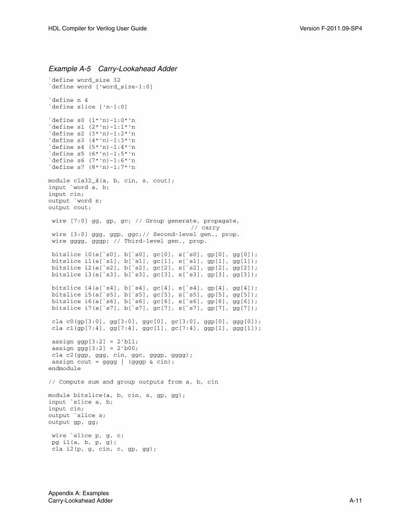
HDL Compiler for Verilog User Guide Version F-2011.09-SP4
Example A-5 Carry-Lookahead Adder`define word_size 32 `define word [‘word_size-1:0]
`define n 4`define slice [‘n-1:0]
`define s0 (1*‘n)-1:0*‘n`define s1 (2*‘n)-1:1*‘n`define s2 (3*‘n)-1:2*‘n`define s3 (4*‘n)-1:3*‘n`define s4 (5*‘n)-1:4*‘n`define s5 (6*‘n)-1:5*‘n`define s6 (7*‘n)-1:6*‘n`define s7 (8*‘n)-1:7*‘n
module cla32_4(a, b, cin, s, cout);input `word a, b;input cin;output `word s;output cout;
wire [7:0] gg, gp, gc; // Group generate, propagate,// carry
wire [3:0] ggg, ggp, ggc;// Second-level gen., prop. wire gggg, gggp; // Third-level gen., prop.
bitslice i0(a[`s0], b[`s0], gc[0], s[`s0], gp[0], gg[0]); bitslice i1(a[`s1], b[`s1], gc[1], s[`s1], gp[1], gg[1]); bitslice i2(a[`s2], b[`s2], gc[2], s[`s2], gp[2], gg[2]); bitslice i3(a[`s3], b[`s3], gc[3], s[`s3], gp[3], gg[3]);
bitslice i4(a[`s4], b[`s4], gc[4], s[`s4], gp[4], gg[4]); bitslice i5(a[`s5], b[`s5], gc[5], s[`s5], gp[5], gg[5]); bitslice i6(a[`s6], b[`s6], gc[6], s[`s6], gp[6], gg[6]); bitslice i7(a[`s7], b[`s7], gc[7], s[`s7], gp[7], gg[7]);
cla c0(gp[3:0], gg[3:0], ggc[0], gc[3:0], ggp[0], ggg[0]); cla c1(gp[7:4], gg[7:4], ggc[1], gc[7:4], ggp[1], ggg[1]);
assign ggp[3:2] = 2'b11; assign ggg[3:2] = 2'b00; cla c2(ggp, ggg, cin, ggc, gggp, gggg); assign cout = gggg | (gggp & cin);endmodule
// Compute sum and group outputs from a, b, cin
module bitslice(a, b, cin, s, gp, gg);input `slice a, b;input cin;output `slice s;output gp, gg;
wire `slice p, g, c; pg i1(a, b, p, g); cla i2(p, g, cin, c, gp, gg);
Chapter A: Examples Carry-Lookahead Adder A-11Appendix A: Examples Carry-Lookahead Adder A-11

HDL Compiler for Verilog User Guide F-2011.09-SP4HDL Compiler for Verilog User Guide Version F-2011.09-SP4
sum i3(a, b, c, s);endmodule
// compute propagate and generate from input bits
module pg(a, b, p, g);input `slice a, b;output `slice p, g;
assign p = a | b; assign g = a & b;endmodule
// compute sum from the input bits and the carries
module sum(a, b, c, s);input `slice a, b, c;output `slice s;
wire `slice t = a ^ b; assign s = t ^ c;endmodule
// n-bit carry-lookahead block
module cla(p, g, cin, c, gp, gg);input `slice p, g;// propagate and generate bitsinput cin; // carry inoutput `slice c; // carry produced for each bitoutput gp, gg; // group generate and group propagate
function [99:0] do_cla; input `slice p, g; input cin;
begin : label integer i; reg gp, gg; reg `slice c; gp = p[0]; gg = g[0]; c[0] = cin; for (i = 1; i < `n; i = i+1) begin gp = gp & p[i]; gg = (gg & p[i]) | g[i]; c[i] = (c[i-1] & p[i-1]) | g[i-1]; end do_cla = {c, gp, gg}; end endfunction
assign {c, gp, gg} = do_cla(p, g, cin);endmodule
Appendix A: Examples Carry-Lookahead Adder A-12
HDL Compiler for Verilog User Guide Version F-2011.09-SP4
Coding for Late-Arriving Signals
The following sections discuss coding techniques for late-arriving signals:
• Datapath Duplication
• Moving Late-Arriving Signals Closer to the Output
Note that these techniques apply to HDL Compiler output. When this output is constrained and optimized by Design Compiler, your structure might be changed, depending on such factors as your design constraints and option settings. See the Design Compiler documentation for details.
Datapath DuplicationThe following examples illustrate how to duplicate logic to improve timing. In Example A-6, CONTROL is a late-arriving input signal that selects between two inputs. The selected input drives a chain of arithmetic operations and ends at the output port COUNT. Note that CONTROL is needed to complete the first operation. In Example A-6, notice that there is a SELECT_OP next to a subtracter. (For more information about SELECT_OP, see “SELECT_OP Inference” on page 3-13.) When you see a SELECT_OP next to an operator, you can usually move it to after the operator by duplicating the logic in the branches of the conditional statement that implied the SELECT_OP. Example A-7 shows this datapath duplication.
When you duplicate the operations that depend on the inputs PTR1 and PTR2, the assignment to COUNT becomes a selection between the two parallel datapaths. The signal CONTROL selects the datapath. The path from CONTROL to the output port COUNT is no longer the critical path, but this change comes at the expense of duplicated logic.
In Example A-7, the entire datapath is duplicated, because CONTROL arrives late. Had CONTROL arrived earlier, you could have duplicated only a portion of the logic, thereby decreasing the area expense. The designer controls how much logic is duplicated.
Chapter A: Examples Coding for Late-Arriving Signals A-13Appendix A: Examples Coding for Late-Arriving Signals A-13
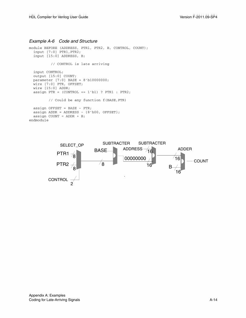
HDL Compiler for Verilog User Guide F-2011.09-SP4HDL Compiler for Verilog User Guide Version F-2011.09-SP4
Example A-6 Code and Structuremodule BEFORE (ADDRESS, PTR1, PTR2, B, CONTROL, COUNT); input [7:0] PTR1,PTR2; input [15:0] ADDRESS, B;
// CONTROL is late arriving
input CONTROL; output [15:0] COUNT; parameter [7:0] BASE = 8'b10000000; wire [7:0] PTR, OFFSET; wire [15:0] ADDR; assign PTR = (CONTROL == 1'b1) ? PTR1 : PTR2;
// Could be any function f(BASE,PTR)
assign OFFSET = BASE - PTR; assign ADDR = ADDRESS - {8'h00, OFFSET}; assign COUNT = ADDR + B;endmodule
SELECT_OP
2
PTR1
PTR2
CONTROL
SUBTRACTER SUBTRACTER
ADDERBASE
800000000
16COUNT
16
B16
8
8
16ADDRESS
Appendix A: Examples Coding for Late-Arriving Signals A-14
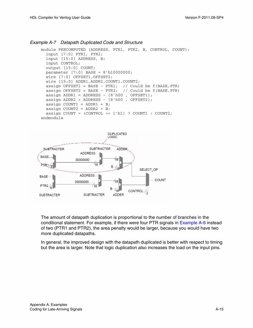
HDL Compiler for Verilog User Guide Version F-2011.09-SP4
Example A-7 Datapath Duplicated Code and Structure
module PRECOMPUTED (ADDRESS, PTR1, PTR2, B, CONTROL, COUNT); input [7:0] PTR1, PTR2; input [15:0] ADDRESS, B; input CONTROL; output [15:0] COUNT; parameter [7:0] BASE = 8'b10000000; wire [7:0] OFFSET1,OFFSET2; wire [15:0] ADDR1,ADDR2,COUNT1,COUNT2; assign OFFSET1 = BASE - PTR1; // Could be f(BASE,PTR) assign OFFSET2 = BASE - PTR2; // Could be f(BASE,PTR) assign ADDR1 = ADDRESS - {8'h00 , OFFSET1}; assign ADDR2 = ADDRESS - {8'h00 , OFFSET2}; assign COUNT1 = ADDR1 + B; assign COUNT2 = ADDR2 + B; assign COUNT = (CONTROL == 1'b1) ? COUNT1 : COUNT2;endmodule
The amount of datapath duplication is proportional to the number of branches in the conditional statement. For example, if there were four PTR signals in Example A-6 instead of two (PTR1 and PTR2), the area penalty would be larger, because you would have two more duplicated datapaths.
In general, the improved design with the datapath duplicated is better with respect to timing but the area is larger. Note that logic duplication also increases the load on the input pins.
Chapter A: Examples Coding for Late-Arriving Signals A-15Appendix A: Examples Coding for Late-Arriving Signals A-15

HDL Compiler for Verilog User Guide F-2011.09-SP4HDL Compiler for Verilog User Guide Version F-2011.09-SP4
Moving Late-Arriving Signals Closer to the OutputDesigners usually know which signals in a design are late-arriving. This knowledge can be used to structure HDL so that the late-arriving signals are close to the output. The following sections give examples of if and case statements for late-arriving signals:
• Overview
• Late-Arriving Data Signal
• Recoding for Late-Arriving Data Signal: Case 1
• Recoding for Late-Arriving Data Signal: Case 2
• Late-Arriving Control Signal
• Recoding for Late-Arriving Control Signal
OverviewSequential if statements allow you to create a priority-encoded implementation that can help in handling late-arriving signals. Assignment priority is from bottom to top, that is, the last if statement in your code translates to the data signal in the last SELECT_OP in the chain of SELECT_OPs as shown in Example A-8.
Example A-8 Sequential if Statements
module mult_if(a, b, c, d, sel, z); input a, b, c, d; input [3:0] sel; output z; reg z; always @(a or b or c or d or sel) begin
z = 0;if (sel[0]) z = a;if (sel[1]) z = b;if (sel[2]) z = c;if (sel[3]) z = d;
endendmodule
Appendix A: Examples Coding for Late-Arriving Signals A-16
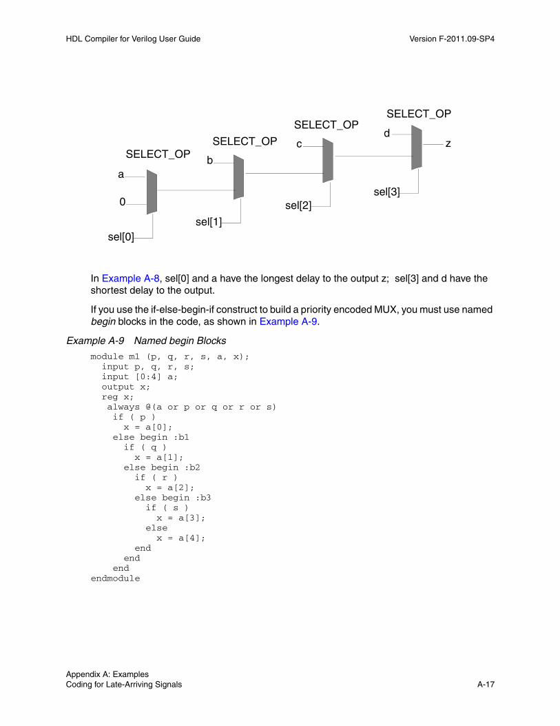
HDL Compiler for Verilog User Guide Version F-2011.09-SP4
SELECT_OPSELECT_OP
SELECT_OPSELECT_OP
zd
sel[3]
c
ba
0 sel[2]
sel[1]sel[0]
In Example A-8, sel[0] and a have the longest delay to the output z; sel[3] and d have the shortest delay to the output.
If you use the if-else-begin-if construct to build a priority encoded MUX, you must use named begin blocks in the code, as shown in Example A-9.
Example A-9 Named begin Blocks
module m1 (p, q, r, s, a, x); input p, q, r, s; input [0:4] a; output x; reg x; always @(a or p or q or r or s) if ( p ) x = a[0]; else begin :b1 if ( q ) x = a[1]; else begin :b2 if ( r ) x = a[2]; else begin :b3 if ( s ) x = a[3]; else x = a[4]; end end endendmodule
Chapter A: Examples Coding for Late-Arriving Signals A-17Appendix A: Examples Coding for Late-Arriving Signals A-17

HDL Compiler for Verilog User Guide F-2011.09-SP4HDL Compiler for Verilog User Guide Version F-2011.09-SP4
SELECT_OP SELECT_OP SELECT_OPSELECT_OP
a[0:4]
s
r
p
q
x
Late-Arriving Data SignalExample A-10 shows code designed to accommodate the late-arriving data signal, b_is_late. This code has b_is_late as close as possible to the output z.
Example A-10 Late-Arriving Data Signal
module mult_if_improved(a, b_is_late, c, d, sel, z); input a, b_is_late, c, d;input [3:0] sel;output z;reg z, z1;
always @(a or b_is_late or c or d or sel)begin
z1 = 0;if (sel[0])z1 = a;if (sel[2])
z1 = c;if (sel[3])
z1 = d;if (sel[1] & ~(sel[2]|sel[3]))
z = b_is_late;else
z = z1;end
endmodule
Appendix A: Examples Coding for Late-Arriving Signals A-18

HDL Compiler for Verilog User Guide Version F-2011.09-SP4
SELECT_OPSELECT_OP
SELECT_OPSELECT_OP
zd
sel[3]
c
b_is_late
a
0 sel[3]2sel[2]
2sel[0]2
sel[2]sel[1]
sel[3]
ControlLogic
2
Recoding for Late-Arriving Data Signal: Case 1Example A-11 shows code that contains operators in the conditional expression of an if statement; Figure A-2 shows the structure implied by the code. The signal A in the conditional expression is a late-arriving signal, so you should move the signal closer to the output.
Example A-11 Input A Is Late-Arrivingmodule cond_oper (A, B, C, D, Z); parameter N = 8;
// A is late arriving
input [N-1:0] A, B, C, D; output [N-1:0] Z; reg [N-1:0] Z; always @(A or B or C or D) begin if (A + B < 24) Z <= C; else Z <= D; endendmodule
Chapter A: Examples Coding for Late-Arriving Signals A-19Appendix A: Examples Coding for Late-Arriving Signals A-19

HDL Compiler for Verilog User Guide F-2011.09-SP4HDL Compiler for Verilog User Guide Version F-2011.09-SP4
Figure A-2 Original Structure
ADDERA
B COMPARATOR
SELECT_OPC
DZ
24
2
Example A-12 restructures the code to do this; Figure A-3 shows the resulting implementation.
Example A-12 Improved Verilog With Operator in Conditional Expression
module cond_oper_improved (A, B, C, D, Z); parameter N = 8;
// A is late arriving
input [N-1:0] A, B, C, D; output [N-1:0] Z; reg [N-1:0] Z; always @(A or B or C or D) begin if ( B < 24 && A < 24 - B) Z <= C; else Z <= D; end
Figure A-3 Recoded Structure
Appendix A: Examples Coding for Late-Arriving Signals A-20

HDL Compiler for Verilog User Guide Version F-2011.09-SP4
Recoding for Late-Arriving Data Signal: Case 2Example A-13 shows a case statement nested in an if statement. The data signal DATA_is_late_arriving is late-arriving.
Example A-13 Original Code
module case_in_if_01(A, DATA_is_late_arriving, C, sel, Z);input [8:1] A;input DATA_is_late_arriving;input [2:0] sel;input [5:1] C;output Z;reg Z;
always @ (sel or C or A or DATA_is_late_arriving)beginif (C[1])
Z = A[5];else if (C[2] == 1'b0)
Z = A[4];else if (C[3])
Z = A[1];else if (C[4])
case (sel)3'b010: Z = A[8];3'b011: Z = DATA_is_late_arriving;3'b101: Z = A[7];3'b110: Z = A[6];default: Z = A[2];
endcaseelse if (C[5] == 1'b0)
Z = A[2];else
Z = A[3];end
endmodule
Figure A-4 shows the structure implied by the code in Example A-13.
Chapter A: Examples Coding for Late-Arriving Signals A-21Appendix A: Examples Coding for Late-Arriving Signals A-21
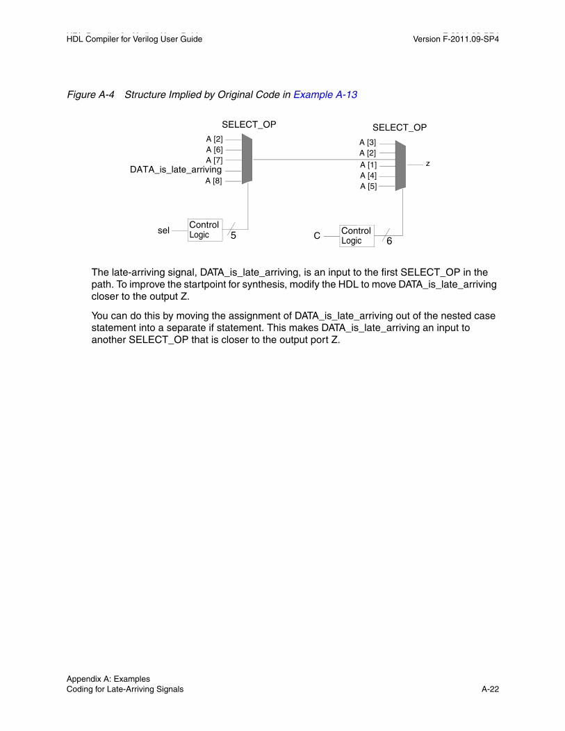
HDL Compiler for Verilog User Guide F-2011.09-SP4HDL Compiler for Verilog User Guide Version F-2011.09-SP4
Figure A-4 Structure Implied by Original Code in Example A-13
A [2]A [6]A [7]
A [8]
SELECT_OP
5
DATA_is_late_arriving
sel
A [3]A [2]
A [1]A [4]A [5]
z
SELECT_OP
6LogicControlCLogic
Control
The late-arriving signal, DATA_is_late_arriving, is an input to the first SELECT_OP in the path. To improve the startpoint for synthesis, modify the HDL to move DATA_is_late_arriving closer to the output Z.
You can do this by moving the assignment of DATA_is_late_arriving out of the nested case statement into a separate if statement. This makes DATA_is_late_arriving an input to another SELECT_OP that is closer to the output port Z.
Appendix A: Examples Coding for Late-Arriving Signals A-22
HDL Compiler for Verilog User Guide Version F-2011.09-SP4
Example A-14 shows the improved version of the code shown in Example A-13.
Example A-14 Improved Code module case_in_if_01_improved(A,DATA_is_late_arriving,C,sel,Z);
input [8:1] A;input DATA_is_late_arriving;input [2:0] sel;input [5:1] C;output Z;reg Z;reg Z1, FIRST_IF;
always @(sel or C or A or DATA_is_late_arriving)beginif (C[1])
Z1 = A[5];else if (C[2] == 1'b0)
Z1= A[4];else if (C[3])
Z1 = A[1];else if (C[4])
case (sel)3'b010: Z1 = A[8];
//3'b011: Z1 = DATA_is_late_arriving;3'b101: Z1 = A[7];3'b110: Z1 = A[6];default: Z1 = A[2];
endcaseelse if (C[5] == 1'b0)
Z1 = A[2];else
Z1 = A[3];
FIRST_IF = (C[1] == 1'b1) || (C[2] == 1'b0) || (C[3] == 1'b1);
if (!FIRST_IF && C[4] && (sel == 3'b011))Z = DATA_is_late_arriving;
elseZ = Z1;
endendmodule
The structure implied by the modified HDL in Example A-14 is given in Figure A-5.
Chapter A: Examples Coding for Late-Arriving Signals A-23Appendix A: Examples Coding for Late-Arriving Signals A-23
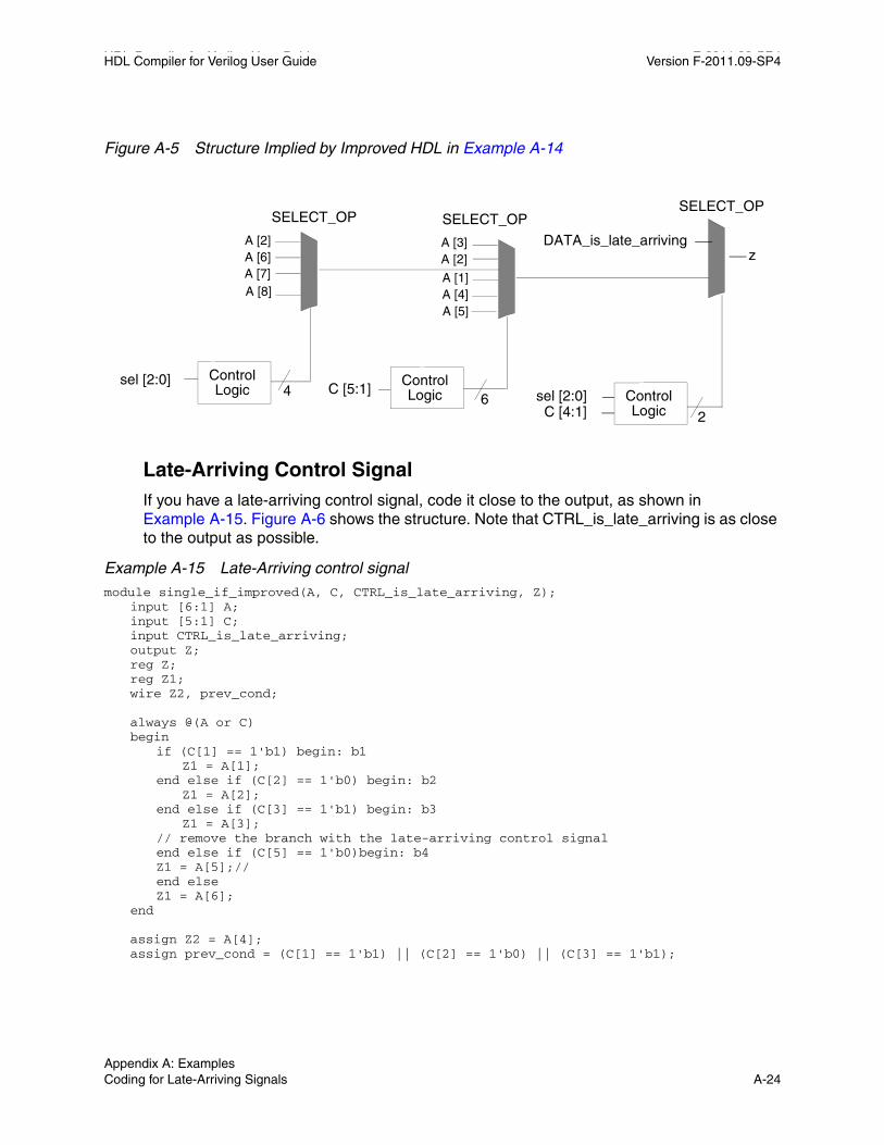
HDL Compiler for Verilog User Guide F-2011.09-SP4HDL Compiler for Verilog User Guide Version F-2011.09-SP4
Figure A-5 Structure Implied by Improved HDL in Example A-14
A [2]A [6]A [7]A [8]
SELECT_OP
4
DATA_is_late_arriving
sel [2:0]
A [3]A [2]
A [1]A [4]A [5]
SELECT_OP
6C [5:1]
z
SELECT_OP
2
sel [2:0]C [4:1] Logic
ControlLogicControl
LogicControl
Late-Arriving Control SignalIf you have a late-arriving control signal, code it close to the output, as shown in Example A-15. Figure A-6 shows the structure. Note that CTRL_is_late_arriving is as close to the output as possible.
Example A-15 Late-Arriving control signalmodule single_if_improved(A, C, CTRL_is_late_arriving, Z);
input [6:1] A;input [5:1] C;input CTRL_is_late_arriving;output Z;reg Z;reg Z1;wire Z2, prev_cond;
always @(A or C)begin
if (C[1] == 1'b1) begin: b1Z1 = A[1];
end else if (C[2] == 1'b0) begin: b2Z1 = A[2];
end else if (C[3] == 1'b1) begin: b3Z1 = A[3];
// remove the branch with the late-arriving control signalend else if (C[5] == 1'b0)begin: b4 Z1 = A[5];//end elseZ1 = A[6];
end
assign Z2 = A[4];assign prev_cond = (C[1] == 1'b1) || (C[2] == 1'b0) || (C[3] == 1'b1);
Appendix A: Examples Coding for Late-Arriving Signals A-24
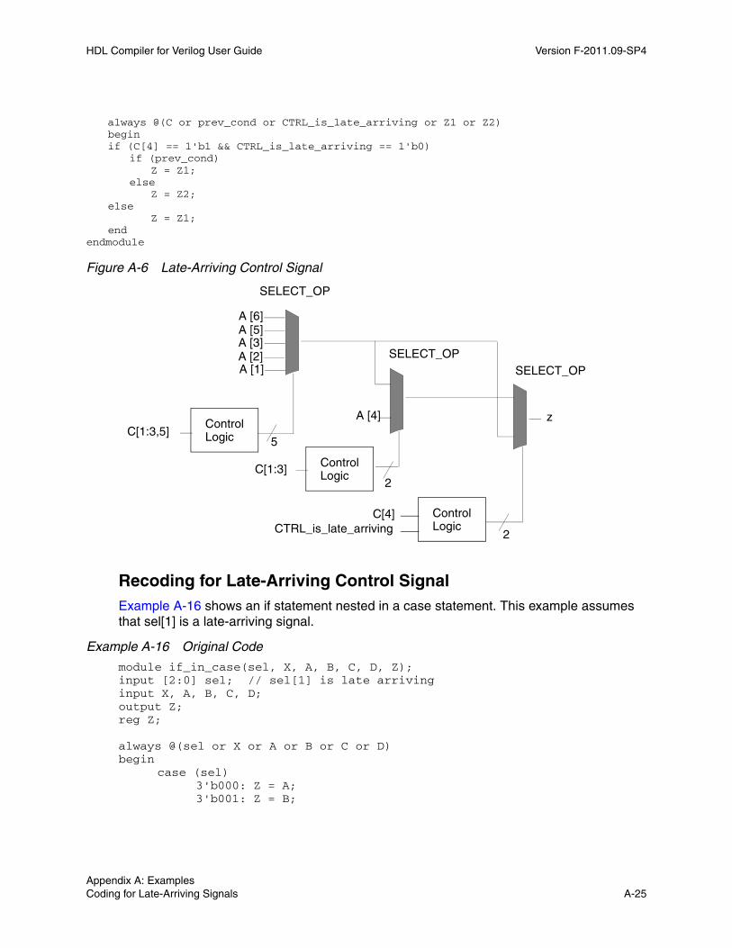
HDL Compiler for Verilog User Guide Version F-2011.09-SP4
always @(C or prev_cond or CTRL_is_late_arriving or Z1 or Z2)beginif (C[4] == 1'b1 && CTRL_is_late_arriving == 1'b0)
if (prev_cond)Z = Z1;
elseZ = Z2;
elseZ = Z1;
endendmodule
Figure A-6 Late-Arriving Control Signal
A [6] A [5]A [3]A [2]A [1]
SELECT_OP
ControlLogic 5
C[1:3,5]
SELECT_OPSELECT_OP
A [4] z
C[1:3]2
C[4]CTRL_is_late_arriving 2
ControlLogic
ControlLogic
Recoding for Late-Arriving Control SignalExample A-16 shows an if statement nested in a case statement. This example assumes that sel[1] is a late-arriving signal.
Example A-16 Original Code
module if_in_case(sel, X, A, B, C, D, Z);input [2:0] sel; // sel[1] is late arrivinginput X, A, B, C, D;output Z;reg Z;
always @(sel or X or A or B or C or D)begin
case (sel)3'b000: Z = A;3'b001: Z = B;
Chapter A: Examples Coding for Late-Arriving Signals A-25Appendix A: Examples Coding for Late-Arriving Signals A-25

HDL Compiler for Verilog User Guide F-2011.09-SP4HDL Compiler for Verilog User Guide Version F-2011.09-SP4
3'b010: if (X == 1'b1)Z = C;
elseZ = D;
3'b100: Z = A ^ B;3'b101: Z = !(A && B);3'b111: Z = !A; default: Z = !B;
endcaseendendmodule
In Example A-16, you know that sel[1] is a late-arriving input. Therefore, you should restructure the code in Example A-16 to get the best startpoint for synthesis.
Example A-17 shows modified code that shifts the dependency on sel[1] closer to the output; that is, it moves sel[1] closer to the output and the nested if statement is removed and placed outside the case statement. This code computes two possible values for z into new variables z1 and z2. These represent what the final value of z will be if sel[1] is 0 and 1, respectively. Then, a final if statement checks the actual value of sel[1] to select between z1 and z2. Because sel[1] is closer to the output, it improves timing if sel[1] is late.
Example A-17 Improved Code
module if_in_case_improved(sel, X, A, B, C, D, Z);input [2:0] sel; // sel[1] is late arrivinginput X, A, B, C, D;output Z;reg Z;reg Z1, Z2;reg [1:0] i_sel;
always @ (sel or X or A or B or C or D)begini_sel = {sel[2],sel[0]};case (i_sel) // for sel[1]=0
2'b00: Z1 = A;2'b01: Z1 = B;2'b10: Z1 = A ^ B;2'b11: Z1 = !(A && B);default: Z1 = !B;
endcase
case (i_sel) // for sel[1]=12'b00:if (X == 1'b1)
Z2 = C;else
Z2 = D;2'b11: Z2 = !A;default: Z2 = !B;
endcaseif (sel[1])
Appendix A: Examples Coding for Late-Arriving Signals A-26
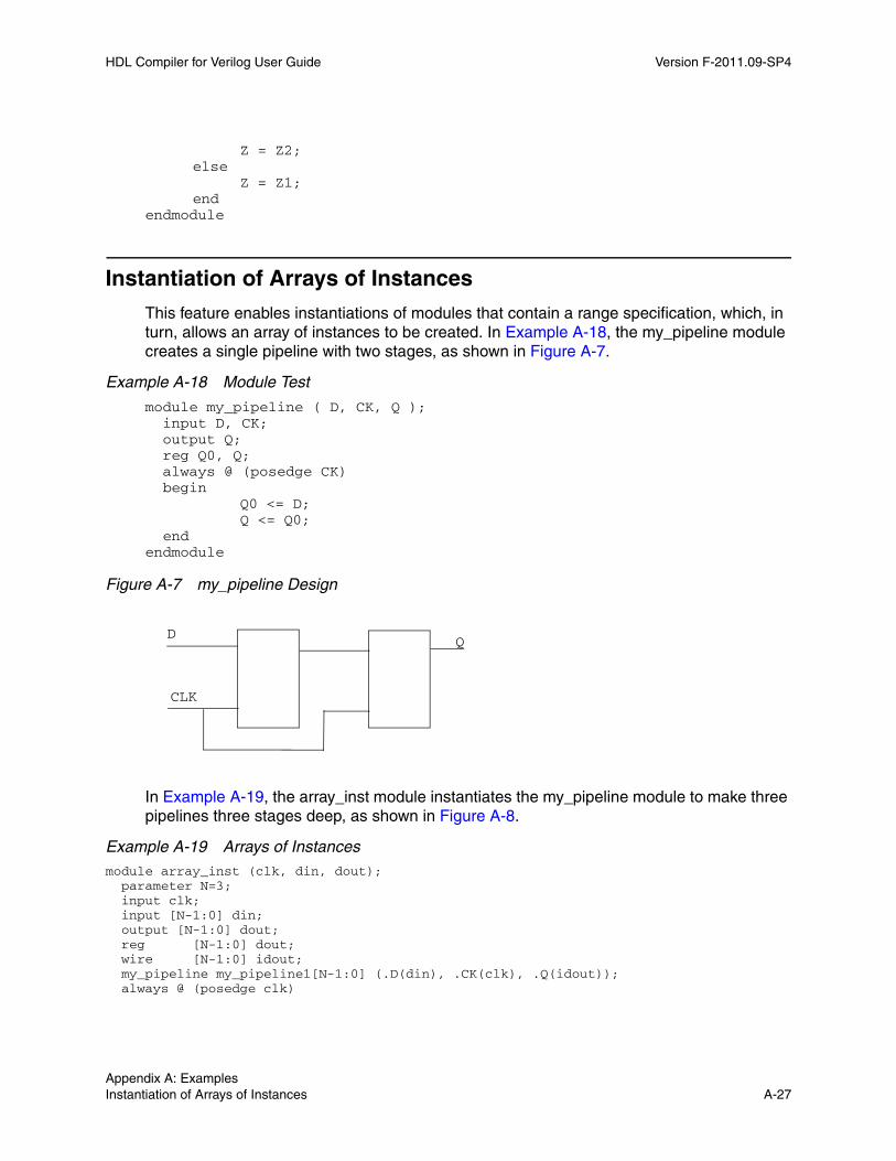
HDL Compiler for Verilog User Guide Version F-2011.09-SP4
Z = Z2;else
Z = Z1;end
endmodule
Instantiation of Arrays of Instances
This feature enables instantiations of modules that contain a range specification, which, in turn, allows an array of instances to be created. In Example A-18, the my_pipeline module creates a single pipeline with two stages, as shown in Figure A-7.
Example A-18 Module Test
module my_pipeline ( D, CK, Q ); input D, CK; output Q; reg Q0, Q; always @ (posedge CK) begin
Q0 <= D;Q <= Q0;
endendmodule
Figure A-7 my_pipeline Design
DQ
CLK
In Example A-19, the array_inst module instantiates the my_pipeline module to make three pipelines three stages deep, as shown in Figure A-8.
Example A-19 Arrays of Instancesmodule array_inst (clk, din, dout); parameter N=3; input clk; input [N-1:0] din; output [N-1:0] dout; reg [N-1:0] dout; wire [N-1:0] idout; my_pipeline my_pipeline1[N-1:0] (.D(din), .CK(clk), .Q(idout)); always @ (posedge clk)
Chapter A: Examples Instantiation of Arrays of Instances A-27Appendix A: Examples Instantiation of Arrays of Instances A-27
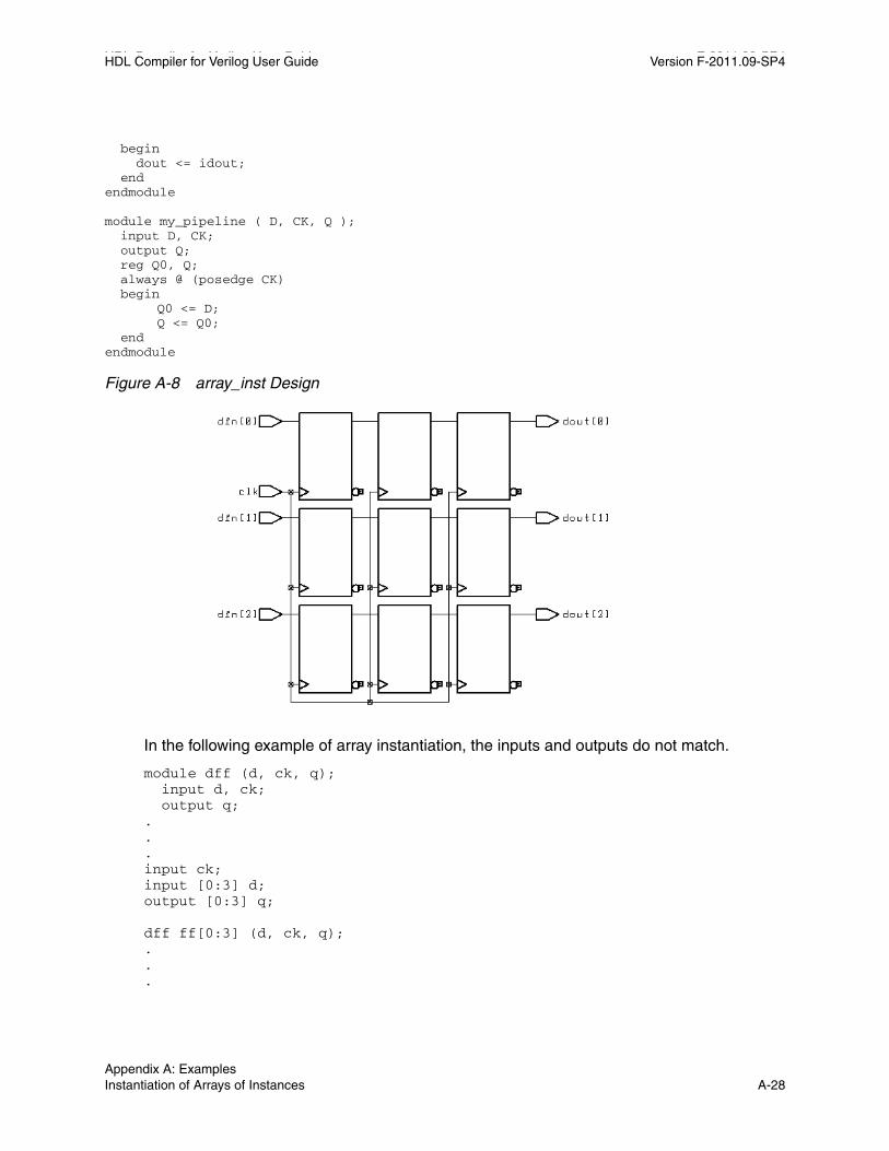
HDL Compiler for Verilog User Guide F-2011.09-SP4HDL Compiler for Verilog User Guide Version F-2011.09-SP4
begin dout <= idout; endendmodule
module my_pipeline ( D, CK, Q ); input D, CK; output Q; reg Q0, Q; always @ (posedge CK) begin
Q0 <= D;Q <= Q0;
endendmodule
Figure A-8 array_inst Design
In the following example of array instantiation, the inputs and outputs do not match.
module dff (d, ck, q); input d, ck; output q;...input ck;input [0:3] d;output [0:3] q;
dff ff[0:3] (d, ck, q);...
Appendix A: Examples Instantiation of Arrays of Instances A-28
HDL Compiler for Verilog User Guide Version F-2011.09-SP4
Here, four copies of the dff module are instantiated. HDL Compiler unrolls the array instantiation as follows:
input ck;input [0:3] d;output [0:3] q;
dff ff_0 (d[0], ck, q[0]);dff ff_1 (d[1], ck, q[1]);dff ff_2 (d[2], ck, q[2]);dff ff_3 (d[3], ck, q[3]);
Note that ck is connected to each instance, whereas d and q have one bit connected to each instance.
In this next example of array instantiation, x exactly matches the width of d on the submodule, so its full width is connected to each instantiated module.
module submod (d, ck, q); input [0:3] d; input ck; output q;...input ck;input [0:3] x;output [0:3] y;
submod ff[0:3] (x, ck, y);
HDL Compiler unrolls the array instantiation as follows:
input ck;input [0:3] d;output [0:3] q;
submod M_0 (x, ck, y[0]);submod M_1 (x, ck, y[1]);submod M_2 (x, ck, y[2]);submod M_3 (x, ck, y[3]);
In this next example of array instantiation, note that the declared ordering of bits [3:0] of y does not affect the instantiation of submod (compare it to the previous example). Bits are connected by position, not by number.
module submod (d, ck, q); input [0:3] d; input ck; output q;...
Chapter A: Examples Instantiation of Arrays of Instances A-29Appendix A: Examples Instantiation of Arrays of Instances A-29
HDL Compiler for Verilog User Guide F-2011.09-SP4HDL Compiler for Verilog User Guide Version F-2011.09-SP4
input ck;input [0:3] x;output [3:0] y;
submod ff[0:3] (x, ck, y);
HDL Compiler unrolls the array instantiation as follows:
input ck;input [0:3] d;output [0:3] q;
submod M_0 (x, ck, y[0]);submod M_1 (x, ck, y[1]);submod M_2 (x, ck, y[2]);submod M_3 (x, ck, y[3]);
SR Latches
Use SR latches with caution because they are difficult to test. If you decide to use SR latches, verify that the inputs are hazard-free (that they do not glitch). During synthesis, Design Compiler does not ensure that the logic driving the inputs is hazard-free.
Example A-20 shows the Verilog code that implements an inferred SR latch whose truth table is described in Table A-1. Example A-21 shows the inference report.
Table A-1 SR Latch Truth Table (NAND Type)
set reset y
0 0 Not stable
0 1 1
1 0 0
1 1 y
Appendix A: Examples SR Latches A-30
HDL Compiler for Verilog User Guide Version F-2011.09-SP4
Example A-20 SR Latch Code
module sr_latch (SET, RESET, Q); input SET, RESET; output Q; reg Q;
//synopsys async_set_reset"SET,RESET" always @(RESET or SET) if (~RESET) Q = 0; else if (~SET) Q = 1;endmodule
Example A-21 SR Latch Inference Report ===========================================================================| Register Name | Type | Width | Bus | MB | AR | AS | SR | SS | ST |===========================================================================| Q_reg | Latch | 1 | N | N | Y | Y | - | - | - |===========================================================================
D Latch With Asynchronous Set: Use async_set_reset
Example A-22 shows the recommended coding style for an asynchronously set latch using the async_set_reset directive.
Example A-22 D Latch With Asynchronous Set: Uses async_set_reset
module d_latch_async_set (GATE, DATA, SET, Q); input GATE, DATA, SET; output Q; reg Q;
//synopsys async_set_reset "SET" always @(GATE or DATA or SET) if (~SET) Q = 1'b1; else if (GATE) Q = DATA;endmodule
HDL Compiler generates the inference report shown in Example A-23.
Example A-23 Inference Report for D Latch With Asynchronous Set===========================================================================| Register Name | Type | Width | Bus | MB | AR | AS | SR | SS | ST |===========================================================================| Q_reg | Latch | 1 | N | N | N | Y | - | - | - |===========================================================================
Chapter A: Examples D Latch With Asynchronous Set: Use async_set_reset A-31Appendix A: Examples D Latch With Asynchronous Set: Use async_set_reset A-31
HDL Compiler for Verilog User Guide F-2011.09-SP4HDL Compiler for Verilog User Guide Version F-2011.09-SP4
Inferring Master-Slave Latches
Master-slave latches are described in the following sections:
• Master-Slave Latch Overview
• Master-Slave Latch With Single Master-Slave Clock Pair
• Master-Slave Latch With Multiple Master-Slave Clock Pairs
• Master-Slave Latch With Discrete Components
Master-Slave Latch OverviewDesign Compiler infers master-slave latches by using the clocked_on_also attribute. This is a special signal-type attribute that must be applied using an embedded dc_script.
In your RTL description, describe the master-slave latch as a flip-flop, using only the slave clock. Specify the master clock as an input port, but do not connect it. In addition, set the clocked_on_also attribute on the master clock port.
This coding style requires that cells in the target technology library contain slave clocks defined with the clocked_on_also attribute. The clocked_on_also attribute defines the slave clocks in the cell’s state declaration. For more information about defining slave clocks in the target technology library, see the Library Compiler User Guide.
Design Compiler does not use D flip-flops to implement the equivalent functionality of the cell.
Note: Although the vendor’s component behaves as a master-slave latch, Library Compiler supports only the description of a master-slave flip-flop.
Master-Slave Latch With Single Master-Slave Clock PairExample A-24 provides the template for a master-slave latch.
See “dc_tcl_script_begin and dc_tcl_script_end” on page 7-4 for more information on the dc_tcl_script_begin and dc_tcl_script_end compiler directives. HDL Compiler generates the verbose inference report shown in Example A-25.
Example A-24 Master-Slave Latch
module mslatch (SCK, MCK, DATA, Q); input SCK, MCK, DATA; output Q; reg Q;
Appendix A: Examples Inferring Master-Slave Latches A-32
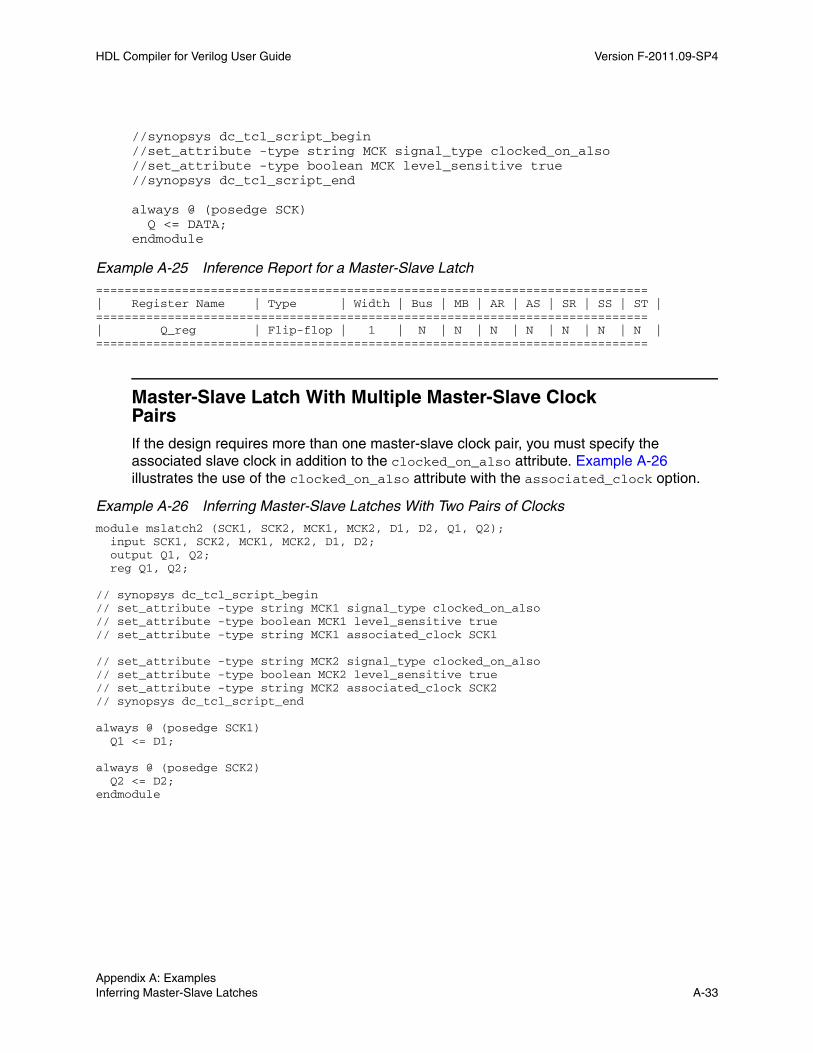
HDL Compiler for Verilog User Guide Version F-2011.09-SP4
//synopsys dc_tcl_script_begin//set_attribute -type string MCK signal_type clocked_on_also//set_attribute -type boolean MCK level_sensitive true//synopsys dc_tcl_script_end
always @ (posedge SCK) Q <= DATA;endmodule
Example A-25 Inference Report for a Master-Slave Latch=============================================================================| Register Name | Type | Width | Bus | MB | AR | AS | SR | SS | ST |=============================================================================| Q_reg | Flip-flop | 1 | N | N | N | N | N | N | N |=============================================================================
Master-Slave Latch With Multiple Master-Slave Clock PairsIf the design requires more than one master-slave clock pair, you must specify the associated slave clock in addition to the clocked_on_also attribute. Example A-26 illustrates the use of the clocked_on_also attribute with the associated_clock option.
Example A-26 Inferring Master-Slave Latches With Two Pairs of Clocksmodule mslatch2 (SCK1, SCK2, MCK1, MCK2, D1, D2, Q1, Q2); input SCK1, SCK2, MCK1, MCK2, D1, D2; output Q1, Q2; reg Q1, Q2;
// synopsys dc_tcl_script_begin// set_attribute -type string MCK1 signal_type clocked_on_also// set_attribute -type boolean MCK1 level_sensitive true// set_attribute -type string MCK1 associated_clock SCK1
// set_attribute -type string MCK2 signal_type clocked_on_also// set_attribute -type boolean MCK2 level_sensitive true// set_attribute -type string MCK2 associated_clock SCK2// synopsys dc_tcl_script_end
always @ (posedge SCK1) Q1 <= D1;
always @ (posedge SCK2) Q2 <= D2;endmodule
Chapter A: Examples Inferring Master-Slave Latches A-33Appendix A: Examples Inferring Master-Slave Latches A-33

HDL Compiler for Verilog User Guide F-2011.09-SP4HDL Compiler for Verilog User Guide Version F-2011.09-SP4
Example A-27 shows the inference reports.
Example A-27 Inference Reports=============================================================================| Register Name | Type | Width | Bus | MB | AR | AS | SR | SS | ST |=============================================================================| Q1_reg | Flip-flop | 1 | N | N | N | N | N | N | N |=============================================================================
=============================================================================| Register Name | Type | Width | Bus | MB | AR | AS | SR | SS | ST |=============================================================================| Q2_reg | Flip-flop | 1 | N | N | N | N | N | N | N |=============================================================================
Master-Slave Latch With Discrete ComponentsIf your target technology library does not contain master-slave latch components, you can infer two-phase systems by using D latches. Example A-28 shows a simple two-phase system with clocks MCK and SCK.
Example A-28 Two-Phase Clocks
module latch_verilog (DATA, MCK, SCK, Q); input DATA, MCK, SCK; output Q; reg Q;
reg TEMP;
always @(DATA or MCK) if (MCK) TEMP <= DATA;
always @(TEMP or SCK) if (SCK) Q <= TEMP;endmodule
Appendix A: Examples Inferring Master-Slave Latches A-34
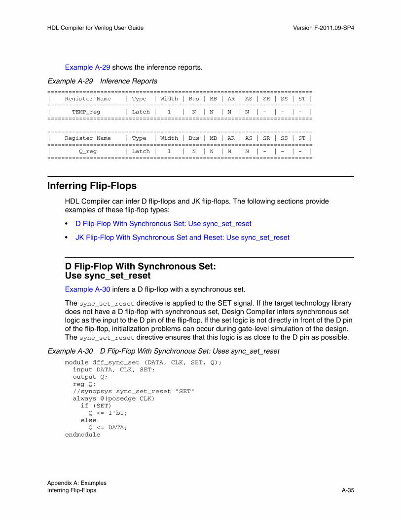
HDL Compiler for Verilog User Guide Version F-2011.09-SP4
Example A-29 shows the inference reports.
Example A-29 Inference Reports===========================================================================| Register Name | Type | Width | Bus | MB | AR | AS | SR | SS | ST |===========================================================================| TEMP_reg | Latch | 1 | N | N | N | N | - | - | - |===========================================================================
===========================================================================| Register Name | Type | Width | Bus | MB | AR | AS | SR | SS | ST |===========================================================================| Q_reg | Latch | 1 | N | N | N | N | - | - | - |===========================================================================
Inferring Flip-Flops
HDL Compiler can infer D flip-flops and JK flip-flops. The following sections provide examples of these flip-flop types:
• D Flip-Flop With Synchronous Set: Use sync_set_reset
• JK Flip-Flop With Synchronous Set and Reset: Use sync_set_reset
D Flip-Flop With Synchronous Set: Use sync_set_reset Example A-30 infers a D flip-flop with a synchronous set.
The sync_set_reset directive is applied to the SET signal. If the target technology library does not have a D flip-flop with synchronous set, Design Compiler infers synchronous set logic as the input to the D pin of the flip-flop. If the set logic is not directly in front of the D pin of the flip-flop, initialization problems can occur during gate-level simulation of the design. The sync_set_reset directive ensures that this logic is as close to the D pin as possible.
Example A-30 D Flip-Flop With Synchronous Set: Uses sync_set_reset
module dff_sync_set (DATA, CLK, SET, Q); input DATA, CLK, SET; output Q; reg Q; //synopsys sync_set_reset "SET" always @(posedge CLK) if (SET) Q <= 1'b1; else Q <= DATA;endmodule
Chapter A: Examples Inferring Flip-Flops A-35Appendix A: Examples Inferring Flip-Flops A-35
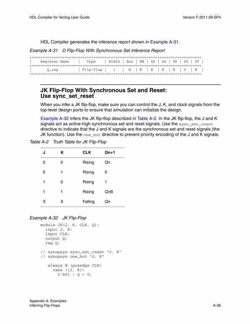
HDL Compiler for Verilog User Guide F-2011.09-SP4HDL Compiler for Verilog User Guide Version F-2011.09-SP4
HDL Compiler generates the inference report shown in Example A-31.
Example A-31 D Flip-Flop With Synchronous Set Inference Report==============================================================================| Register Name | Type | Width | Bus | MB | AR | AS | SR | SS | ST |==============================================================================| Q_reg | Flip-flop | 1 | N | N | N | N | N | Y | N |==============================================================================
JK Flip-Flop With Synchronous Set and Reset: Use sync_set_resetWhen you infer a JK flip-flop, make sure you can control the J, K, and clock signals from the top-level design ports to ensure that simulation can initialize the design.
Example A-32 infers the JK flip-flop described in Table A-2. In the JK flip-flop, the J and K signals act as active-high synchronous set and reset signals. Use the sync_set_reset directive to indicate that the J and K signals are the synchronous set and reset signals (the JK function). Use the one_hot directive to prevent priority encoding of the J and K signals.
Table A-2 Truth Table for JK Flip-Flop
J K CLK Qn+1
0 0 Rising Qn
0 1 Rising 0
1 0 Rising 1
1 1 Rising QnB
X X Falling Qn
Example A-32 JK Flip-Flop
module JK(J, K, CLK, Q); input J, K; input CLK; output Q; reg Q;
// synopsys sync_set_reset "J, K"// synopsys one_hot "J, K"
always @ (posedge CLK) case ({J, K}) 2'b01 : Q = 0;
Appendix A: Examples Inferring Flip-Flops A-36

HDL Compiler for Verilog User Guide Version F-2011.09-SP4
2'b10 : Q = 1; 2'b11 : Q = ~Q; endcaseendmodule
Example A-33 shows the inference report generated by HDL Compiler.
Example A-33 Inference Report==============================================================================| Register Name | Type | Width | Bus | MB | AR | AS | SR | SS | ST |==============================================================================| Q_reg | Flip-flop | 1 | N | N | N | N | Y | Y | N |==============================================================================
Chapter A: Examples Inferring Flip-Flops A-37Appendix A: Examples Inferring Flip-Flops A-37

HDL Compiler for Verilog User Guide F-2011.09-SP4HDL Compiler for Verilog User Guide Version F-2011.09-SP4
Appendix A: Examples Inferring Flip-Flops A-38

BVerilog Language Support B
The following sections describe the Verilog language as supported by HDL Compiler:
• Syntax
• Verilog Keywords
• Unsupported Verilog Language Constructs
• Construct Restrictions and Comments
• Verilog 2001 and 2005 Supported Constructs
• Ignored Constructs
• Verilog 2001 Feature Examples
• Verilog 2005 Feature Example
B-1
HDL Compiler for Verilog User Guide F-2011.09-SP4HDL Compiler for Verilog User Guide Version F-2011.09-SP4
Syntax
Synopsys supports the Verilog syntax as described in the IEEE STD 1364-2001.
The lexical conventions HDL Compiler uses are described in the following sections:
• Comments
• Numbers
CommentsYou can enter comments anywhere in a Verilog description, in two forms:
• Beginning with two slashes //
HDL Compiler ignores all text between these characters and the end of the current line.
• Beginning with the two characters /* and ending with */
HDL Compiler ignores all text between these characters, so you can continue comments over more than one line.
Note: You cannot nest comments.
Numbers You can declare numbers in several different radices and bit-widths. A radix is the base number on which a numbering system is built. For example, the binary numbering system has a radix of 2, octal has a radix of 8, and decimal has a radix of 10.
You can use these three number formats:
• A simple decimal number that is a sequence of digits in the range of 0 to 9. All constants declared this way are assumed to be 32-bit numbers.
• A number that specifies the bit-width as well as the radix. These numbers are the same as those in the previous format, except that they are preceded by a decimal number that specifies the bit-width.
• A number followed by a two-character sequence prefix that specifies the number’s size and radix. The radix determines which symbols you can include in the number. Constants declared this way are assumed to be 32-bit numbers. Any of these numbers can include underscores ( _ ), which improve readability and do not affect the value of the number. Table B-1 summarizes the available radices and valid characters for the number.
Appendix B: Verilog Language Support Syntax B-2
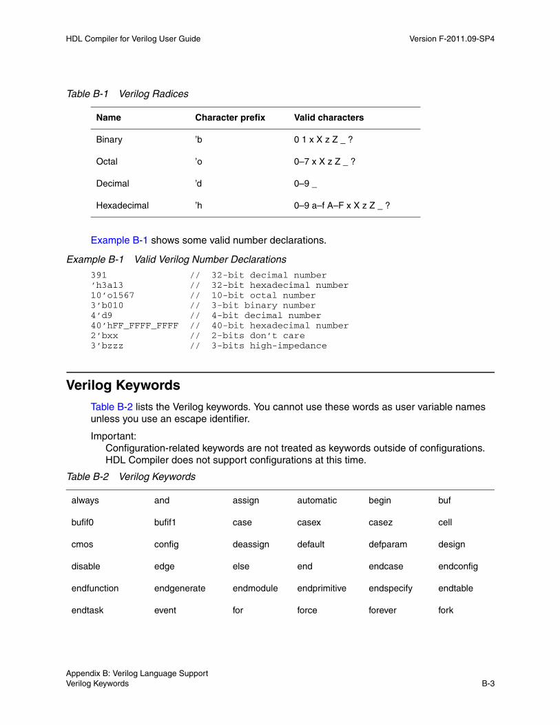
HDL Compiler for Verilog User Guide Version F-2011.09-SP4
Table B-1 Verilog Radices
Name Character prefix Valid characters
Binary ’b 0 1 x X z Z _ ?
Octal ’o 0–7 x X z Z _ ?
Decimal ’d 0–9 _
Hexadecimal ’h 0–9 a–f A–F x X z Z _ ?
Example B-1 shows some valid number declarations.
Example B-1 Valid Verilog Number Declarations
391 // 32-bit decimal number’h3a13 // 32-bit hexadecimal number10’o1567 // 10-bit octal number3’b010 // 3-bit binary number4’d9 // 4-bit decimal number40’hFF_FFFF_FFFF // 40-bit hexadecimal number2’bxx // 2-bits don’t care3’bzzz // 3-bits high-impedance
Verilog Keywords
Table B-2 lists the Verilog keywords. You cannot use these words as user variable names unless you use an escape identifier.
Important: Configuration-related keywords are not treated as keywords outside of configurations. HDL Compiler does not support configurations at this time.
Table B-2 Verilog Keywords
always and assign automatic begin buf
bufif0 bufif1 case casex casez cell
cmos config deassign default defparam design
disable edge else end endcase endconfig
endfunction endgenerate endmodule endprimitive endspecify endtable
endtask event for force forever fork
Chapter B: Verilog Language Support Verilog Keywords B-3Appendix B: Verilog Language Support Verilog Keywords B-3

HDL Compiler for Verilog User Guide F-2011.09-SP4HDL Compiler for Verilog User Guide Version F-2011.09-SP4
Unsupported Verilog Language Constructs
HDL Compiler does not support the following constructs:
• Configurations
• Unsupported definitions and declarations
❍ primitive definition
❍ time declaration
❍ event declaration
function generate genvar highz0 highz1 if
ifnone incdir include initial inout input
instance integer join large liblist library
localparam macromodule medium module nand negedge
nmos nor noshowcancelled
not notif0 notif1
or output parameter pmos posedge primitive
pull0 pull1 pulldown pullup pulsestyle_ onevent
pulsestyle_ondetect
rcmos real realtime reg release repeat
rnmos rpmos rtran rtranif0 rtranif1 scalared
showcancelled signed small specify specparam strong0
strong1 supply0 supply1 table task time
tran tranif0 tranif1 tri tri0 tri1
triand trior trireg unsigned use vectored
wait wand weak0 weak1 while wire
wor xnor xor
Table B-2 Verilog Keywords (Continued)
Appendix B: Verilog Language Support Unsupported Verilog Language Constructs B-4
HDL Compiler for Verilog User Guide Version F-2011.09-SP4
❍ triand, trior, tri1, tri0, and trireg net types
❍ Ranges for integers
• Unsupported statements
❍ initial statement
❍ repeat statement
❍ delay control
❍ event control
❍ forever statement (The forever loop is only supported if it has an associated disable condition, making the exit condition deterministic.)
❍ fork statement
❍ deassign statement
❍ force statement
❍ release statement
• Unsupported operators
❍ Case equality and inequality operators (=== and !==)
• Unsupported gate-level constructs
❍ nmos, pmos, cmos, rnmos, rpmos, rcmos
❍ pullup, pulldown, tranif0, tranif1, rtran, rtrainf0, and rtrainf1 gate types
• Unsupported miscellaneous constructs
❍ hierarchical names within a module
If you use an unsupported construct, HDL Compiler issues a syntax error such as
event is not supported
Construct Restrictions and Comments
Construct restrictions and guidelines are described in the following section:
• always Blocks
• generate Statements
• Conditional Expressions (?:) Resource Sharing
Chapter B: Verilog Language Support Construct Restrictions and Comments B-5Appendix B: Verilog Language Support Construct Restrictions and Comments B-5

HDL Compiler for Verilog User Guide F-2011.09-SP4HDL Compiler for Verilog User Guide Version F-2011.09-SP4
• Case
• defparam
• disable
• Blocking and Nonblocking Assignments
• Macromodule
• inout Port Declaration
• tri Data Type
• HDL Compiler Directives
• reg Types
• Types in Busing
• Combinational while Loops
always BlocksThe tool does not support more than one independent if-block when asynchronous behavior is modeled within an always block. If the always block is purely synchronous, the tool supports multiple independent if-blocks. In addition, the tool does not support more than one ?: operator inside an always block.
generate StatementsSynopsys support of the generate statement is described in the following sections:
• Generate Overview
• Restrictions
Generate OverviewHDL Compiler supports both the 2001 and the 2005 standards for the generate statement. The default is the 2005 standard; to enable the 2001 standard, set the hdlin_vrlg_std variable to 2001. The following subsections describe the naming-style differences between these two standards.
Appendix B: Verilog Language Support Construct Restrictions and Comments B-6
HDL Compiler for Verilog User Guide Version F-2011.09-SP4
Types of generate Blocks
Standalone generate Blocks
Standalone generate blocks are blocks using the begin statement that are not associated with a conditional generate or loop generate block. These are legal under the 2001 standard, but are illegal according to the Verilog 2005 LRM, as illustrated in the following example.
Example B-2 Standalone generate Block
module top ( input in1, output out1 ); generate begin : b1 mod1 U1(in1, out1);endendgenerate endmodule
module mod1( input in1, output out1 );endmodule
When you use the 2001 standard, HDL Compiler creates the name b1.U1 for mod 1:
Cell Reference Library Area Attributes-------------------------------------------------------------------b1.U1 mod1 0.000000 b-------------------------------------------------------------------Total 1 cells 0.000000
When you use the 2005 standard, HDL Compiler issues a VER-946 error message:
Compiling source file RTL/t1.vError: RTL/t1.v:3: Syntax error on an obsolete Verilog 2001 construct standalone generate block 'b1'. (VER-946)*** HDLC compilation terminated with 1 errors. ***
Anonymous generate BlocksAnonymous generate blocks are generate blocks that do not have a user-defined label. They are also referred to as unnamed blocks.
According to the 2001 Verilog LRM, anonymous blocks do not create their own scope, but the 2005 standard has an implicit naming convention that allows scope creation. The Verilog 2005 standard assigns a number to every generate construct in a given scope. The number is 1 for the first construct and is incremented by 1 for each subsequent generate construct in the scope. All unnamed generate blocks are given the name genblkn, where n is the number assigned to the enclosing generate construct. If the name conflicts with an explicitly declared name, leading zeroes are added in front of the number until the conflict is resolved.
The examples that follow illustrate the difference between the two standards.
Chapter B: Verilog Language Support Construct Restrictions and Comments B-7Appendix B: Verilog Language Support Construct Restrictions and Comments B-7
HDL Compiler for Verilog User Guide F-2011.09-SP4HDL Compiler for Verilog User Guide Version F-2011.09-SP4
Example B-3 Anonymous generate Block
module top( input [0:3] in1, output [0:3] out1 );genvar I;generatefor( I = 0; I < 3; I = I+1 ) begin: b1 if( 1 ) begin : b2 if( 1 ) if( 1 ) if( 1 ) mod1 U1(in1[I], out1[I]); endendendgenerateendmodule
module mod1( input in1, output out1 );endmodule
When you use the Verilog 2001 standard, HDL Compiler creates the names b1[0].b2.U1, b1[1].b2.U1, and b1[2].b2.U1 for the instantiated subblocks:
Cell Reference Library Area Attributes-------------------------------------------------------------------------b1[0].b2.U1 mod1 0.000000 bb1[1].b2.U1 mod1 0.000000 bb1[2].b2.U1 mod1 0.000000 b-------------------------------------------------------------------------Total 3 cells 0.000000
When you use the Verilog 2005 standard, HDL Compiler creates the names b1[0].b2.genblk1.U1, b1[1].b2.genblk1.U1, and b1[2].b2.genblk1.U1. Note that there are no multiple genblk1's for the nested anonymous if blocks:
Cell Reference Library Area Attributes-------------------------------------------------------------------------b1[0].b2.genblk1.U1 mod1 0.000000 bb1[1].b2.genblk1.U1 mod1 0.000000 bb1[2].b2.genblk1.U1 mod1 0.000000 b-------------------------------------------------------------------------Total 3 cells 0.000000
Another type of anonymous generate block is created when the block does not have a label, but each block has a begin ...end statement:
Example B-4 Anonymous generate Block with begin...end
module top( input [0:3] in1, output [0:3] out1 );genvar I;generatefor( I = 0; I < 3; I = I+1 ) begin: b1 if( 1 ) begin : b2 if( 1 ) begin if( 1 ) begin
Appendix B: Verilog Language Support Construct Restrictions and Comments B-8
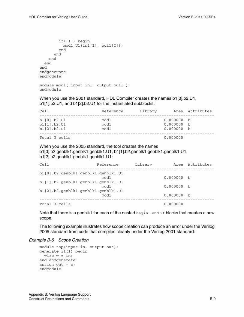
HDL Compiler for Verilog User Guide Version F-2011.09-SP4
if( 1 ) begin mod1 U1(in1[I], out1[I]); end end end endendendgenerateendmodule
module mod1( input in1, output out1 );endmodule
When you use the 2001 standard, HDL Compiler creates the names b1[0].b2.U1, b1[1].b2.U1, and b1[2].b2.U1 for the instantiated subblocks:
Cell Reference Library Area Attributes-------------------------------------------------------------------------b1[0].b2.U1 mod1 0.000000 bb1[1].b2.U1 mod1 0.000000 bb1[2].b2.U1 mod1 0.000000 b-------------------------------------------------------------------------Total 3 cells 0.000000
When you use the 2005 standard, the tool creates the names b1[0].b2.genblk1.genblk1.genblk1.U1, b1[1].b2.genblk1.genblk1.genblk1.U1, b1[2].b2.genblk1.genblk1.genblk1.U1:
Cell Reference Library Area Attributes-------------------------------------------------------------------------b1[0].b2.genblk1.genblk1.genblk1.U1 mod1 0.000000 bb1[1].b2.genblk1.genblk1.genblk1.U1 mod1 0.000000 bb1[2].b2.genblk1.genblk1.genblk1.U1 mod1 0.000000 b-------------------------------------------------------------------------Total 3 cells 0.000000
Note that there is a genblk1 for each of the nested begin...end if blocks that creates a new scope.
The following example illustrates how scope creation can produce an error under the Verilog 2005 standard from code that compiles cleanly under the Verilog 2001 standard:
Example B-5 Scope Creation
module top(input in, output out);generate if(1) begin wire w = in;end endgenerateassign out = w;endmodule
Chapter B: Verilog Language Support Construct Restrictions and Comments B-9Appendix B: Verilog Language Support Construct Restrictions and Comments B-9
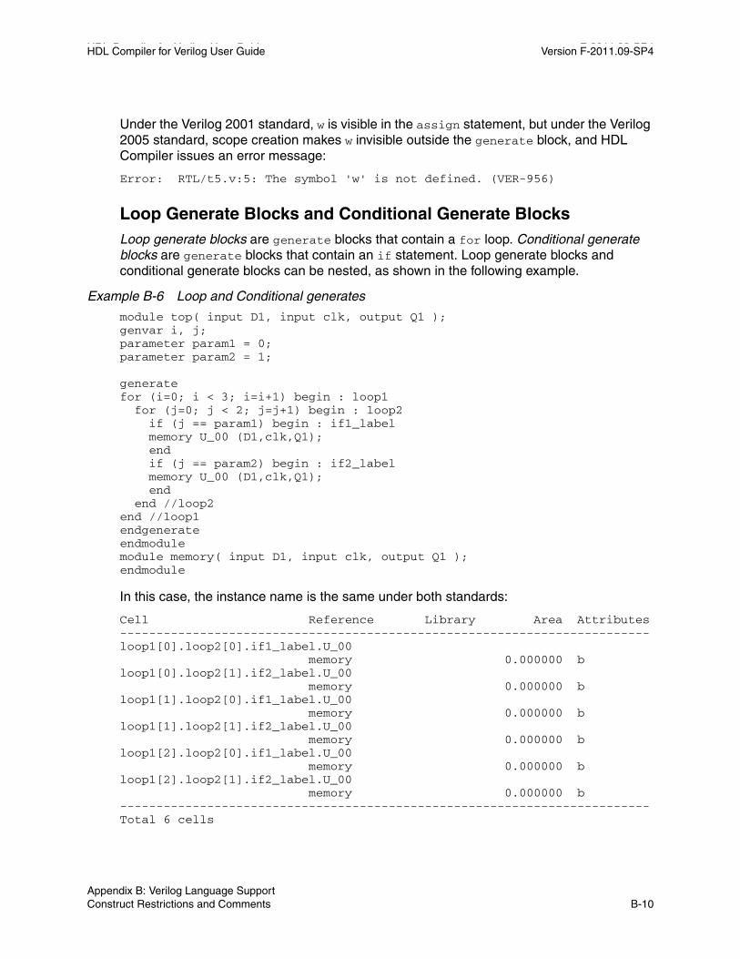
HDL Compiler for Verilog User Guide F-2011.09-SP4HDL Compiler for Verilog User Guide Version F-2011.09-SP4
Under the Verilog 2001 standard, w is visible in the assign statement, but under the Verilog 2005 standard, scope creation makes w invisible outside the generate block, and HDL Compiler issues an error message:
Error: RTL/t5.v:5: The symbol 'w' is not defined. (VER-956)
Loop Generate Blocks and Conditional Generate BlocksLoop generate blocks are generate blocks that contain a for loop. Conditional generate blocks are generate blocks that contain an if statement. Loop generate blocks and conditional generate blocks can be nested, as shown in the following example.
Example B-6 Loop and Conditional generates
module top( input D1, input clk, output Q1 );genvar i, j;parameter param1 = 0;parameter param2 = 1;
generatefor (i=0; i < 3; i=i+1) begin : loop1 for (j=0; j < 2; j=j+1) begin : loop2 if (j == param1) begin : if1_label memory U_00 (D1,clk,Q1); end if (j == param2) begin : if2_label memory U_00 (D1,clk,Q1); end end //loop2end //loop1endgenerateendmodulemodule memory( input D1, input clk, output Q1 );endmodule
In this case, the instance name is the same under both standards:
Cell Reference Library Area Attributes-------------------------------------------------------------------------loop1[0].loop2[0].if1_label.U_00 memory 0.000000 bloop1[0].loop2[1].if2_label.U_00 memory 0.000000 bloop1[1].loop2[0].if1_label.U_00 memory 0.000000 bloop1[1].loop2[1].if2_label.U_00 memory 0.000000 bloop1[2].loop2[0].if1_label.U_00 memory 0.000000 bloop1[2].loop2[1].if2_label.U_00 memory 0.000000 b-------------------------------------------------------------------------Total 6 cells
Appendix B: Verilog Language Support Construct Restrictions and Comments B-10

HDL Compiler for Verilog User Guide Version F-2011.09-SP4
Restrictions• Hierarchical Names (Cross Module Reference)
HDL Compiler supports hierarchical names or cross-module references, if the hierarchical name remains inside the module that contains the name and each item on the hierarchical path is part of the module containing the reference.
In the following code, the item is not part of the module and is not supported.
module top (); wire x; down d (); endmodule
module down (); wire y, z; assign t = top.d.z; // not supported: // hier. ref. starts outside current module endmodule
• Parameter Override (defparam)
The use of defparam is highly discouraged in synthesis because of ambiguity problems. Because of these problems, defparam is not supported inside generate blocks. For details, see the Verilog 1800 LRM.
Conditional Expressions (?:) Resource SharingHDL Compiler supports resource sharing in conditional expressions such as
dout = sel ? (a + b) : (a + c);
In such cases, HDL Compiler marks the adders as sharable; Design Compiler determines the final implementation during timing-drive resource sharing.
The tool does not support more than one ?: operator inside an always block. For more information, see “always Blocks” on page B-6.
Case The case construct is discussed in the following sections:
• casez and casex
• Full Case and Parallel Case
Chapter B: Verilog Language Support Construct Restrictions and Comments B-11Appendix B: Verilog Language Support Construct Restrictions and Comments B-11

HDL Compiler for Verilog User Guide F-2011.09-SP4HDL Compiler for Verilog User Guide Version F-2011.09-SP4
casez and casex HDL Compiler allows ? and z bits in casez items but not in expressions; that is, the z bits are allowed in the branches of the case statement but not in the expression immediately following the casez keyword.
casez (y) // y is referred to as the case expression
2’b1z: //2’b1z is referred to as the item
Example B-7 shows an invalid expression in a casez statement.
Example B-7 Invalid casez Expression
casez (1’bz) //illegal testing of an expression ...endcase
The same holds true for casex statements using x, ?, and z. The code
casex (a)2’b1x : // matches 2’b10 and 2’b11endcase
does not equal the following code:
b = 2’b1x;casex (a)b: // in this case, 2’b1x only matches 2’b10endcase
When x is assigned to a variable and the variable is used in a casex item, the x does not match both 0 and 1 as it would for a literal x listed in the case item.
Full Case and Parallel CaseCase statements can be full or parallel. HDL Compiler can usually determine automatically whether a case statement is full or parallel. Example B-8 shows a case statement that is both full and parallel.
Appendix B: Verilog Language Support Construct Restrictions and Comments B-12
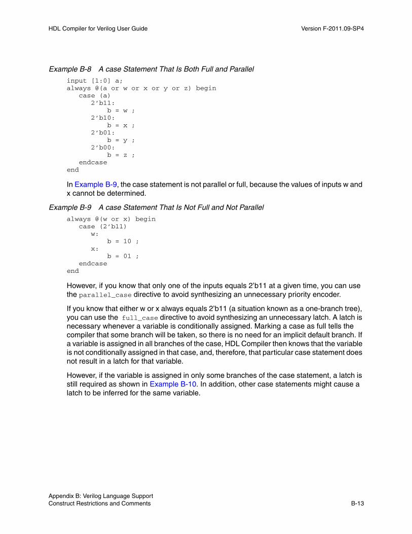
HDL Compiler for Verilog User Guide Version F-2011.09-SP4
Example B-8 A case Statement That Is Both Full and Parallel
input [1:0] a;always @(a or w or x or y or z) begin
case (a)2’b11: b = w ;2’b10: b = x ;2’b01: b = y ;2’b00: b = z ;
endcaseend
In Example B-9, the case statement is not parallel or full, because the values of inputs w and x cannot be determined.
Example B-9 A case Statement That Is Not Full and Not Parallel
always @(w or x) begincase (2’b11)
w: b = 10 ;x: b = 01 ;
endcaseend
However, if you know that only one of the inputs equals 2’b11 at a given time, you can use the parallel_case directive to avoid synthesizing an unnecessary priority encoder.
If you know that either w or x always equals 2’b11 (a situation known as a one-branch tree), you can use the full_case directive to avoid synthesizing an unnecessary latch. A latch is necessary whenever a variable is conditionally assigned. Marking a case as full tells the compiler that some branch will be taken, so there is no need for an implicit default branch. If a variable is assigned in all branches of the case, HDL Compiler then knows that the variable is not conditionally assigned in that case, and, therefore, that particular case statement does not result in a latch for that variable.
However, if the variable is assigned in only some branches of the case statement, a latch is still required as shown in Example B-10. In addition, other case statements might cause a latch to be inferred for the same variable.
Chapter B: Verilog Language Support Construct Restrictions and Comments B-13Appendix B: Verilog Language Support Construct Restrictions and Comments B-13

HDL Compiler for Verilog User Guide F-2011.09-SP4HDL Compiler for Verilog User Guide Version F-2011.09-SP4
Example B-10 Latch Result When Variable Is Not Fully Assigned
reg a, b;reg [1:0] c;case (c) // synopsys full_case 0: begin a = 1; b = 0; end 1: begin a = 0; b = 0; end 2: begin a = 1; b = 1; end 3: b = 1; // a is not assigned hereendcase
For more information, see “parallel_case” on page 7-15 and “full_case” on page 7-7.
defparam Use of defparam is highly discouraged in synthesis because of ambiguity problems. Because of these problems, defparam is not supported inside generate blocks. For details, see the Verilog LRM.
disable HDL Compiler supports the disable statement when you use it in named blocks and when it is used to disable an enclosing block. When a disable statement is executed, it causes the named block to terminate. You cannot disable a block that is not in the same always block or task as the disable statement. A comparator description that uses disable is shown in Example B-11.
Example B-11 Comparator Using disable
begin : compare for (i = 7; i >= 0; i = i - 1) begin
if (a[i] != b[i]) begin greater_than = a[i]; less_than = ~a[i]; equal_to = 0; //comparison is done so stop looping disable compare; end
end
// If you get here a == b // If the disable statement is executed, the next three // lines will not be executed greater_than = 0; less_than = 0; equal_to = 1; end
Appendix B: Verilog Language Support Construct Restrictions and Comments B-14

HDL Compiler for Verilog User Guide Version F-2011.09-SP4
You can also use a disable statement to implement a synchronous reset, as shown in Example B-12.
Example B-12 Synchronous Reset of State Register Using disable in a forever Loop
alwaysbegin: foo
@ (posedge clk)if (Reset)
beginz <= 1’b0;disable foo;
endz <= a;
end
The disable statement in Example B-12 causes the foo block to terminate immediately and return to the beginning of the block.
Blocking and Nonblocking AssignmentsHDL Compiler does not allow both blocking and nonblocking assignments to the same variable within an always block.
The following code applies both blocking and nonblocking assignments to the same variable in one always block.
always @(posedge clk or negedge reset) begin if (~ reset) q = 1’b0; else q <= d;end
HDL Compiler does not permit this and generates an error message.
During simulation, race conditions can result from blocking assignments, as shown in Example B-13. In this example, the value of x is indeterminate, because multiple procedural blocks run concurrently, causing y to be loaded into x at the same time z is loading into y. The value of x after the first @ (posedge clk) is indeterminate. Use of nonblocking assignments solves this race condition, as shown in Example B-14.
In Example B-13 and Example B-14, HDL Compiler creates the gates shown in Figure B-1.
Example B-13 Race Condition Using Blocking Assignments
always @(posedge clk) x = y;always @(posedge clk) y = z;
Chapter B: Verilog Language Support Construct Restrictions and Comments B-15Appendix B: Verilog Language Support Construct Restrictions and Comments B-15

HDL Compiler for Verilog User Guide F-2011.09-SP4HDL Compiler for Verilog User Guide Version F-2011.09-SP4
Example B-14 Race Solved With Nonblocking Assignments
always @(posedge clk) x <= y;always @(posedge clk) y <= x;
Figure B-1 Simulator Race Condition—Synthesis Gates
If you want to switch register values, use nonblocking assignments, because blocking assignments will not accomplish the switch. For example, in Example B-15, the desired outcome is a swap of the x and y register values. However, after the positive clock edge, y does not end up with the value of x; y ends up with the original value of y. This happens because blocking statements are order dependent and each statement within the procedural block is executed before the next statement is evaluated and executed. In Example B-16, the swap is accomplished with nonblocking assignments.
Example B-15 Swap Problem Using Blocking Assignments
always @(posedge clk)begin x = y; y = x;end
Example B-16 Swap Accomplished With Nonblocking Assignments
always @(posedge clk) x <= y; y <= z;
MacromoduleHDL Compiler treats the macromodule construct as a module construct. Whether you use module or macromodule, the synthesis results are the same.
inout Port DeclarationHDL Compiler allows you to connect inout ports only to module or gate instantiations. You must declare an inout before you use it.
Appendix B: Verilog Language Support Construct Restrictions and Comments B-16

HDL Compiler for Verilog User Guide Version F-2011.09-SP4
tri Data TypeThe tri data type allows multiple three-state devices to drive a wire. When inferring three-state devices, you need to ensure that all the drivers are inferred as three-state devices and that all inputs to a device are z, except the one variable driving the three-state device which will have a 1.
HDL Compiler DirectivesHDL compiler directives are discussed in the following sections:
• `define
• `include
• `ifdef, `else, `endif, `ifndef, and `elsif
• `rp_group and `rp_endgroup
• `rp_place
• `rp_fill
• `rp_array_dir
• rp_align
• rp_orient
• rp_ignore and rp_endignore
• `undef
`defineThe `define directive can specify macros that take arguments. For example,
`define BYTE_TO_BITS(arg)((arg) << 3)
The `define directive can do more than simple text substitution. It can also take arguments and substitute their values in its replacement text.
Macro substitution assigns a string of text to a macro variable. The string of text is inserted into the code where the macro is encountered. The definition begins with the back quotation mark (`), followed by the keyword define, followed by the name of the macro variable. All text from the macro variable until the end of the line is assigned to the macro variable.
Chapter B: Verilog Language Support Construct Restrictions and Comments B-17Appendix B: Verilog Language Support Construct Restrictions and Comments B-17

HDL Compiler for Verilog User Guide F-2011.09-SP4HDL Compiler for Verilog User Guide Version F-2011.09-SP4
You can declare and use macro variables anywhere in the description. The definitions can carry across several files that are read into Design Compiler at the same time. To make a macro substitution, type a back quotation mark (`) followed by the macro variable name.
Some sample macro variable declarations are shown in Example B-17.
Example B-17 Macro Variable Declarations
`define highbits 31:29`define bitlist {first, second, third}wire [31:0] bus;`bitlist = bus[‘highbits];
The analyze -define command allows macro definition on the command line. Only one -define per analyze command is allowed but the argument can be a list of macros, as shown in Example B-18.
Note: When using the -define option with multiple analyze commands, you must remove any designs in memory before re-analyzing the design. To remove the designs, use remove_design -all. Because elaborated designs in memory have no timestamps, the tool cannot determine whether the analyzed file has been updated or not. The tool may assume that the previously elaborated design is up-to-date and reuse it.
Curly brackets are not required to enclose one macro, as shown in Example B-19. However, if the argument is a list of macros, curly brackets are required.
Example B-18 analyze Command With List of Defines
analyze -f verilog -define { RIPPLE, SIMPLE } mydesign.v
Example B-19 analyze Command With One Define
analyze -f verilog -define ONLY_ONE mydesign.v
Note: In dctcl mode, the read_verilog command does not accept the -define option.
See also “Predefined Macros” on page 1-18.
`include The ̀ include construct in Verilog is similar to the #include directive in the C language. You can use this construct to include Verilog code, such as type declarations and functions, from one module in another module. Example B-20 shows an application of the `include construct.
Appendix B: Verilog Language Support Construct Restrictions and Comments B-18
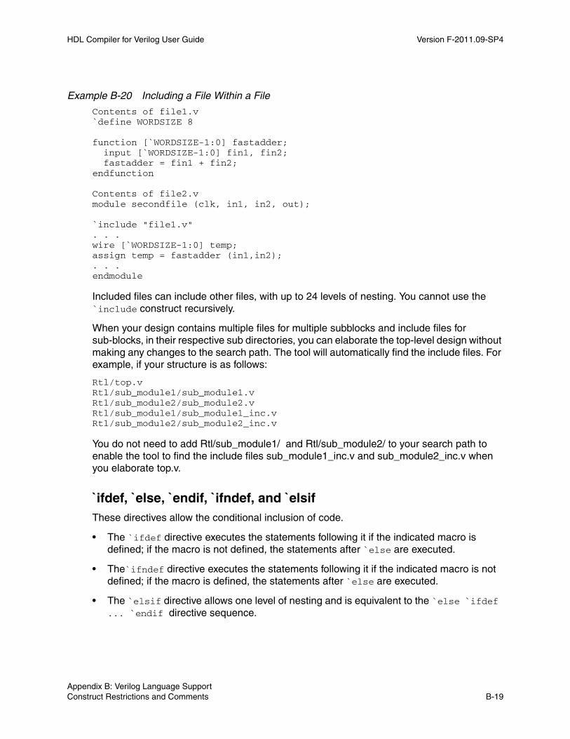
HDL Compiler for Verilog User Guide Version F-2011.09-SP4
Example B-20 Including a File Within a File
Contents of file1.v`define WORDSIZE 8
function [`WORDSIZE-1:0] fastadder; input [`WORDSIZE-1:0] fin1, fin2; fastadder = fin1 + fin2;endfunction
Contents of file2.vmodule secondfile (clk, in1, in2, out);
`include "file1.v". . .wire [`WORDSIZE-1:0] temp;assign temp = fastadder (in1,in2);. . . endmodule
Included files can include other files, with up to 24 levels of nesting. You cannot use the `include construct recursively.
When your design contains multiple files for multiple subblocks and include files for sub-blocks, in their respective sub directories, you can elaborate the top-level design without making any changes to the search path. The tool will automatically find the include files. For example, if your structure is as follows:
Rtl/top.vRtl/sub_module1/sub_module1.vRtl/sub_module2/sub_module2.vRtl/sub_module1/sub_module1_inc.vRtl/sub_module2/sub_module2_inc.v
You do not need to add Rtl/sub_module1/ and Rtl/sub_module2/ to your search path to enable the tool to find the include files sub_module1_inc.v and sub_module2_inc.v when you elaborate top.v.
`ifdef, `else, `endif, `ifndef, and `elsifThese directives allow the conditional inclusion of code.
• The `ifdef directive executes the statements following it if the indicated macro is defined; if the macro is not defined, the statements after `else are executed.
• The`ifndef directive executes the statements following it if the indicated macro is not defined; if the macro is defined, the statements after `else are executed.
• The `elsif directive allows one level of nesting and is equivalent to the `else `ifdef ... `endif directive sequence.
Chapter B: Verilog Language Support Construct Restrictions and Comments B-19Appendix B: Verilog Language Support Construct Restrictions and Comments B-19
HDL Compiler for Verilog User Guide F-2011.09-SP4HDL Compiler for Verilog User Guide Version F-2011.09-SP4
Example B-21 illustrates usage. Use the `define directive to define the macros that are arguments to the `ifdef directive; see “`define” on page B-17.
Example B-21 Design Using `ifdef...`else...`endif Directives
`ifdef SELECT_XOR_DESIGNmodule selective_design(a,b,c); input a, b; output c; assign c = a ^ b;endmodule `else module selective_design(a,b,c); input a, b; output c; assign c = a | b;endmodule`endif
`rp_group and `rp_endgroupThe `rp_group and `rp_endgroup directives allow you to specify a relative placement group. All cell instances declared between the directives are members of the specified group. These directives are available for RTL designs and netlist designs.
The Verilog syntax for RTL designs is as follows:
`rp_group ( group_name {num_cols num_rows} )`rp_endgroup ( {group_name} )
Use the following syntax for netlist designs:
//synopsys rp_group ( group_name {num_cols num_rows} )//synopsys rp_endgroup ( {group_name} )
For more information and an example, see “Creating Groups Using `rp_group and `rp_endgroup” on page 2-4.
`rp_placeThe `rp_place directive allows you to specify a subgroup at a specific hierarchy, a keepout region, or an instance to be placed in the current relative placement group. When you use the `rp_place directive to specify a subgroup at a specific hierarchy, you must instantiate the subgroup’s instances outside of any group declarations in the module. This directive is available for RTL designs and netlist designs.
The Verilog syntax for RTL designs is as follows:
‘rp_place ( hier group_name col row )
Appendix B: Verilog Language Support Construct Restrictions and Comments B-20

HDL Compiler for Verilog User Guide Version F-2011.09-SP4
‘rp_place ( keep keepout_name col row width height )‘rp_place ({leaf} [inst_name] col row )
Use the following syntax for netlist designs:
//synopsys rp_place ( hier group_name col row )//synopsys rp_place ( hier group_name [inst_name] col row )//synopsys rp_place ({leaf} [inst_name] col row )//synopsys rp_place ( keep keepout_name col row width height )
For more information and examples, see “Specifying Subgroups, Keepouts, and Instances Using `rp_place” on page 2-5.
`rp_fillThe `rp_fill directive automatically places the cells at the location specified by a pointer. Each time a new instance is declared that is not explicitly placed, it is inserted into the grid at the location indicated by the current value of the pointer. After the instance is placed, the pointer is updated incrementally and the process is ready to be repeated. This directive is available for RTL designs and netlist designs.
The `rp_fill arguments define how the pointer is updated. The col and row parameters specify the initial coordinates of the pointer. These parameters can represent absolute row or column locations in the group’s grid or locations that are relative to the current pointer value. To represent locations relative to the current pointer, enclose the column and row values in angle brackets (<>). For example, assume the current pointer location is (3,4). In this case, specifying rp_fill <1> 0 initializes the pointer to (4,0) and that is where the next instance is placed. Absolute coordinates must be nonnegative integers; relative coordinates can be any integer.
The Verilog syntax for RTL designs is as follows:
‘rp_fill ( {col row} {pattern pat} )
Use the following syntax for netlist designs:
//synopsys rp_fill ( col row} {pattern pat} )
For more information and an example, see “Placing Cells Automatically Using `rp_fill” on page 2-6.
`rp_array_dirNote:
This directive is available for creating relative placement in RTL designs but not in netlist designs.
Chapter B: Verilog Language Support Construct Restrictions and Comments B-21Appendix B: Verilog Language Support Construct Restrictions and Comments B-21
HDL Compiler for Verilog User Guide F-2011.09-SP4HDL Compiler for Verilog User Guide Version F-2011.09-SP4
The `rp_array_dir directive specifies whether the elements of an array are placed upward, from the least significant bit to the most significant bit, or downward, from the most significant bit to the least significant bit.
The Verilog syntax for RTL designs is as follows:
`rp_array_dir ( up|down )
For more information and an example, see “Specifying Placement for Array Elements Using `rp_array_dir” on page 2-8.
rp_alignThe rp_align directive explicitly specifies the alignment of the placed instance within the grid cell when the instance is smaller than the cell. If you specify the optional inst instance name argument, the alignment applies only to that instance; however, if you do not specify an instance, the new alignment applies to all subsequent instantiations within the group until HDL Compiler encounters another rp_align directive. If the instance straddles cells, the alignment takes place within the straddled region. The alignment value is sw (southwest) by default. The instance is snapped to legal row and routing grid coordinates.
Use the following syntax for netlist designs:
//synopsys rp_align ( n|s|e|w|nw|sw|ne|se|pin=name { inst })
Note: This directive is available for creating relative placement in netlist designs only.
For more information and an example, see “Specifying Cell Alignment Using rp_align” on page 2-8.
rp_orientNote:
This directive is available for creating relative placement in netlist designs only.
The rp_orient directive allows you to control the orientation of library cells placed in the current group. When you specify a list of possible orientations, HDL Compiler chooses the first legal orientation for the cell.
Use the following syntax for netlist designs:
//synopsys rp_orient ( {N|W|S|E|FN|FW|FS|FE}* { inst } )//synopsys rp_orient ( {N|W|S|E|FN|FW|FS|FE}* { group_name inst } ))
For more information and an example, see “Specifying Cell Orientation Using rp_orient” on page 2-9.
Appendix B: Verilog Language Support Construct Restrictions and Comments B-22
HDL Compiler for Verilog User Guide Version F-2011.09-SP4
rp_ignore and rp_endignoreNote:
This directive is available for creating relative placement in netlist designs only.
The rp_ignore and rp_endignore directives allow you to ignore specified lines in the input file. Any lines between the two directives are omitted from relative placement. The include and define directives, variable substitution, and cell mapping are not ignored.
The rp_ignore and rp_endignore directives allow you to include the instantiation of submodules in a relative placement group close to the rp_place hier group(inst) location to place relative placement array.
Use the following syntax for netlist designs:
//synopsys rp_ignore//synopsys rp_endignore
For more information and an example, see “Ignoring Relative Placement Using rp_ignore and rp_endignore” on page 2-10.
`undefThe `undef directive resets the macro immediately following it.
reg TypesThe Verilog language requires that any value assigned inside an always statement must be declared as a reg type. HDL Compiler returns an error if any value assigned inside an always block is not declared as a reg type.
Types in BusingDesign Compiler maintains types throughout a design, including types for buses (vectors). Example B-22 shows a Verilog design read into HDL Compiler containing a bit vector that is NOTed into another bit vector.
Example B-22 Bit Vector in Verilog
module test_busing_1 ( a, b ); input [3:0] a; output [3:0] b;
assign b = ~a;endmodule
Chapter B: Verilog Language Support Construct Restrictions and Comments B-23Appendix B: Verilog Language Support Construct Restrictions and Comments B-23

HDL Compiler for Verilog User Guide F-2011.09-SP4HDL Compiler for Verilog User Guide Version F-2011.09-SP4
Example B-23 shows the same description written out by HDL Compiler. The description contains the original Verilog types of ports. Internal nets do not maintain their original bus types. Also, the NOT operation is instantiated as single bits.
Example B-23 Bit Blasting
module test_busing_2 ( a, b ); input [3:0] a; output [3:0] b; assign b[0] = ~a[0]; assign b[1] = ~a[1]; assign b[2] = ~a[2]; assign b[3] = ~a[3];endmodule
Combinational while Loops To create a combinational while loop, write the code so that an upper bound on the number of loop iterations can be determined. The loop iterative bound must be statically determinable; otherwise an error is reported.
HDL Compiler needs to be able to determine an upper bound on the number of trips through the loop at compile time. In HDL Compiler, there are no syntax restrictions on the loops; while loops that have no events within them, such as in the following example, are supported.
input [9:0] a;// ....i = 0;while ( i < 10 && !a[i] ) begin i = i + 1; // loop bodyend
To support this loop, HDL Compiler interprets it like a simulator. The tool stops when the loop termination condition is known to be false. Because HDL Compiler can’t determine when a loop is infinite, it stops and reports an error after an arbitrary (but user defined) number of iterations (the default is 1024).
To exit the loop, HDL Compiler allows additional conditions in the loop condition that permit more concise descriptions.
for (i = 0; i < 10 && a[i]; i = i+1) begin // loop bodyend
A loop must unconditionally make progress toward termination in each trip through the loop, or it cannot be compiled. The following example makes progress (that is, increments i) only when !done is true and will not terminate.
Appendix B: Verilog Language Support Construct Restrictions and Comments B-24
HDL Compiler for Verilog User Guide Version F-2011.09-SP4
while ( i < 10 ) begin if ( ! done ) done = a[i]; // loop body i = i + 1; endend
The following modified version, which unconditionally increments i, will terminate. This code creates the desired logic.
while ( i < 10 ) begin if ( ! done ) begin done = a[i]; end// loop body i = i + 1;end
In the next example, loop termination depends on reading values stored in x. If the value is unknown (as in the first and third iterations), HDL Compiler assumes it might be true and generates logic to test it.
x[0] = v; // Value unknown: implies “if(v)” x[1] = 1; // Known TRUE: no guard on 2nd tripx[2] = w; // Not known: implies “if(w)”x[3] = 0; // Known FALSE: stop the loop
i = 0;while( x[i] ) begin // loop body i = i + 1;end
This code terminates after three iterations when the loop tests x[3], which contains 0.
In Example B-24, a supported combinational while loop, the code produces gates, and an event control signal is not necessary.
Example B-24 Supported while Loop Code
module modified_s2 (a, b, z);parameter N = 3;input [N:0] a, b;output [N:1] z;reg [N:1] z;integer i;always @(a or b or z) begin i = N; while (i) begin z[i] = b[i] + a[i-1]; i = i - 1;
Chapter B: Verilog Language Support Construct Restrictions and Comments B-25Appendix B: Verilog Language Support Construct Restrictions and Comments B-25

HDL Compiler for Verilog User Guide F-2011.09-SP4HDL Compiler for Verilog User Guide Version F-2011.09-SP4
end endendmodule
In Example B-25, a supported combinational while loop, no matter what x is, the loop will run for 16 iterations at most because HDL Compiler can keep track of which bits of x are constant. Even though it doesn't know the initial value of x, it does know that x >> 1 has a zero in the most significant bit (MSB). The next time x is shifted right, it knows that x has two zeros in the MSB, and so on. HDL Compiler can determine when x becomes all zeros.
Example B-25 Supported Combinational while Loop
module while_loop_comb1(x, count); input [7:0] x; output [2:0] count; reg [7:0] temp; reg [2:0] count; always @ (x) begin temp = x; count = 0; while (temp != 0) begin count = count + 1; temp = temp >> 1;
end endendmodule
In Example B-26, a supported combinational while loop, HDL Compiler knows the initial value of x and can determine x+1 and all subsequent values of x.
Example B-26 Supported Combinational while Loop
module while_loop_comb2(y, count1, z); input [3:0] y, count1;output [3:0] z; reg [3:0] x, z, count; always @ (y, count1) begin x = 2; count = count1; while (x < 15) begin count = count + 1; x = x + 1; end z = count; endendmodule
Appendix B: Verilog Language Support Construct Restrictions and Comments B-26
HDL Compiler for Verilog User Guide Version F-2011.09-SP4
In Example B-27, HDL Compiler cannot detect the initial value of i and so cannot support this while loop. Example B-28 is supported because i is determinable.
Example B-27 Unsupported Combinational while Loopmodule my_loop1 #(parameter N=4) (input [N:0] in, output reg [2*N:0] out); reg [N:0] i; always @* begin i = in; out = 0 ; while (i>0) begin out = out + i; i = i - 1; endendendmodule
Example B-28 Supported Combinational while Loopmodule my_loop2 #(parameter N=4) (input [N:0] in, output reg [2*N:0] out); reg [N:0] i; reg [N+1:0] j; always @* for (j = 0 ; j < (2<<N) ; j = j+1 ) if (j==in) begin i = j; out = 0 ; while (i>0) begin out = out + i; i = i - 1; end endendmodule
Verilog 2001 and 2005 Supported Constructs
Table B-3 lists the Verilog 2001 and 2005 features implemented by HDL Compiler. For additional information on these features, see IEEE Std 1364-2001.
Table B-3 Supported Verilog 2001 and 2005 Constructs
Feature Description
Automatic tasks and functions Fully supported
Constant functions Fully supported
Local parameter Fully supported
generate statement See “generate Statements” on page B-6.
SYNTHESIS macro Fully supported
Chapter B: Verilog Language Support Verilog 2001 and 2005 Supported Constructs B-27Appendix B: Verilog Language Support Verilog 2001 and 2005 Supported Constructs B-27
HDL Compiler for Verilog User Guide F-2011.09-SP4HDL Compiler for Verilog User Guide Version F-2011.09-SP4
Implicit net declarations for continuous assignments
Fully supported
`line directive Fully supported
ANSI-C-style port declarations Fully supported
Casting operators Fully supported
Parameter passing by name (IEEE 12.2.2.2)
Fully supported
Implicit event expression list (IEEE 9.7.5)
Fully supported
ANSI-C-style port declaration (IEEE 12.3.3)
Fully supported
Signed/unsigned parameters (IEEE 3.11)
Fully supported
Signed/unsigned nets and registers (IEEE 3.2, 4.3)
Fully supported
Signed/unsigned sized and based constants (IEEE 3.2)
Fully supported
Multidimensional arrays an arrays of nets (IEEE 3.10)
Fully supported
Part select addressing ([+:] and [-:] operators) (IEEE 4.2.1)
Fully supported
Power operator (**) (IEEE 4.1.5) Fully supported
Arithmetic shift operators (<<< and >>>) (IEEE 4.1.12)
Fully supported
Sized parameters (IEEE 3.11.1) Fully supported
`ifndef, `elsif, `undef (IEEE 19.4,19.3.2) Fully supported
Table B-3 Supported Verilog 2001 and 2005 Constructs (Continued)
Feature Description
Appendix B: Verilog Language Support Verilog 2001 and 2005 Supported Constructs B-28

HDL Compiler for Verilog User Guide Version F-2011.09-SP4
Ignored Constructs
The following sections include directives that HDL Compiler accepts but ignores.
Simulation DirectivesThe following directives are special commands that affect the operation of the Verilog HDL simulator:
'accelerate 'celldefine'default_nettype'endcelldefine 'endprotect'expand_vectornets'noaccelerate 'noexpand_vectornets'noremove_netnames'nounconnected_drive 'protect'remove_netnames'resetall 'timescale'unconnected_drive
You can include these directives in your design description; HDL Compiler accepts but ignores them.
Verilog System FunctionsVerilog system functions are special functions that Verilog HDL simulators implement. Their names start with a dollar sign ($). All of these functions are accepted but ignored by HDL Compiler with the exception of $display, which can be useful during synthesis elaboration. See “Use of $display During RTL Elaboration” on page 1-21.
`ifdef VERILOG_2001 and `ifdef VERILOG_1995
Fully supported
Comma-separated sensitivity lists (IEEE 4.1.15 and 9.7.4)
Fully supported
Table B-3 Supported Verilog 2001 and 2005 Constructs (Continued)
Feature Description
Chapter B: Verilog Language Support Ignored Constructs B-29Appendix B: Verilog Language Support Ignored Constructs B-29
HDL Compiler for Verilog User Guide F-2011.09-SP4HDL Compiler for Verilog User Guide Version F-2011.09-SP4
Verilog 2001 Feature Examples
This section provides examples for Verilog 2001 features in the following sections:
• Multidimensional Arrays and Arrays of Nets
• Signed Quantities
• Comparisons With Signed Types
• Controlling Signs With Casting Operators
• Part-Select Addressing Operators ([+:] and [-:])
• Power Operator (**)
• Arithmetic Shift Operators (<<< and >>>)
Multidimensional Arrays and Arrays of NetsHDL Compiler supports multidimensional arrays of any variable or net data type. This added functionality is shown in examples B-29 through B-32.
Example B-29 Multidimensional Arrays
module m (a, z); input [7:0] a; output z; reg t [0:3][0:7]; integer i, j; integer k; always @(a) begin for (j = 0; j < 8; j = j + 1) begin t[0][j] = a[j]; end for (i = 1; i < 4; i = i + 1) begin k = 1 << (3-i); for (j = 0; j < k; j = j + 1) begin t[i][j] = t[i-1][2*j] ^ t[i-1][2*j+1]; end end end assign z = t[3][0];endmodule
Appendix B: Verilog Language Support Verilog 2001 Feature Examples B-30

HDL Compiler for Verilog User Guide Version F-2011.09-SP4
Example B-30 Arrays of Nets
module m (a, z); input [0:3] a; output z; wire x [0:2] ; assign x[0] = a[0] ^ a[1]; assign x[1] = a[2] ^ a[3]; assign x[2] = x[0] ^ x[1]; assign z = x[2];endmodule
Example B-31 Multidimensional Array Variable Subscripting
reg [7:0] X [0:7][0:7][0:7];
assign out = X[a][b][c][d+:4];
Verilog 2001 allows more than one level of subscripting on a variable, without use of a temporary variable.
Example B-32 Multidimensional Arraymodule test(in, en, out, addr_in, addr_out_reg, addr_out_bit, clk);
input [7:0] in; input en, clk; input [2:0] addr_in, addr_out_reg, addr_out_bit; reg [7:0] MEM [0:7]; output out;
assign out = MEM[addr_out_reg][addr_out_bit];
always @(posedge clk) if (en) MEM[addr_in] = in;endmodule
Signed QuantitiesHDL Compiler supports signed arithmetic extensions. Function returns and reg and net data types can be declared as signed. This added functionality is shown in examples B-33 through B-38.
Example B-33 results in a sign extension, that is, z[0] connects to a[0].
Example B-33 Signed I/O Ports
module m1 (a, z); input signed [0:3] a; output signed [0:4] z; assign z = a;endmodule
Chapter B: Verilog Language Support Verilog 2001 Feature Examples B-31Appendix B: Verilog Language Support Verilog 2001 Feature Examples B-31

HDL Compiler for Verilog User Guide F-2011.09-SP4HDL Compiler for Verilog User Guide Version F-2011.09-SP4
In Example B-34, because 3’sb111 is signed, the tool infers a signed adder. In the generic netlist, the ADD_TC_OP cell denotes a 2’s complement adder and z[0] will not be logic 0.
Example B-34 Signed Constants: Code and GTECH Gates
module m2 (a, z); input signed [0:2] a; output [0:4] z; assign z = a + 3’sb111;endmodule
In Example B-35, because 4’sd5 is signed, a signed comparator (LT_TC_OP) is inferred.
Example B-35 Signed Registers: Code and GTECH Gates
module m3 (a, z); input [0:3] a; output z; reg signed [0:3] x; reg z; always begin x = a; z = x < 4’sd5; endendmodule
In Example B-36, because in1, in2, and out are signed, a signed multiplier (MULT_TC_OP_8_8_8) is inferred.
Example B-36 Signed Types: Code and Gates
module m4 (in1, in2, out); input signed [7:0] in1, in2; output signed [7:0] out; assign out = in1 * in2;endmodule
The code in Example B-37 results in a signed subtracter (SUB_TC_OP).
Example B-37 Signed Nets: Code and Gates
module m5 (a, b, z); input [1:0] a, b; output [2:0] z; wire signed [1:0] x = a; wire signed [1:0] y = b; assign z = x - y;endmodule
Appendix B: Verilog Language Support Verilog 2001 Feature Examples B-32
HDL Compiler for Verilog User Guide Version F-2011.09-SP4
In Example B-38, because 4’sd5 is signed, a signed comparator (LT_TC_OP) is inferred.
Example B-38 Signed Values
module m6 (a, z); input [3:0] a; output z; reg signed [3:0] x; wire z; always @(a) begin x = a; end assign z = x < -4’sd5;endmodule
Verilog 2001 adds the signed keyword in declarations: reg signed [7:0] x;
It also adds support for signed, sized constants. For example, 8'sb11111111 is an 8-bit signed quantity representing -1. If you are assigning it to a variable that is 8 bits or less, 8'sb11111111 is the same as the unsigned 8'b11111111. A behavior difference arises when the variable being assigned to is larger than the constant. This difference occurs because signed quantities are extended with the high-order bit of the constant, whereas unsigned quantities are extended with 0s. When used in expressions, the sign of the constant helps determine whether the operation is performed as signed or unsigned.
HDL Compiler enables signed types by default.
Note: If you use the signed keyword, any signed constant in your code, or explicit type casting between signed and unsigned types, HDL Compiler issues a warning.
Comparisons With Signed TypesVerilog sign rules are tricky. All inputs to an expression must be signed to obtain a signed operator. If one is signed and one unsigned, both are treated as unsigned. Any unsigned quantity in an expression makes the whole expression unsigned; the result doesn’t depend on the sign of the left side. Some expressions always produce an unsigned result; these include bit and part-select and concatenation. See IEEE P1364/P5 Section 4.5.1.
You need to control the sign of the inputs yourself if you want to compare a signed quantity against an unsigned one. The same is true for other kinds of expressions. See Example B-39 and Example B-40.
Chapter B: Verilog Language Support Verilog 2001 Feature Examples B-33Appendix B: Verilog Language Support Verilog 2001 Feature Examples B-33
HDL Compiler for Verilog User Guide F-2011.09-SP4HDL Compiler for Verilog User Guide Version F-2011.09-SP4
Example B-39 Unsigned Comparison Results When Signs Are Mismatched
module m8 (in1, in2, lt);// in1 is signed but in2 is unsigned input signed [7:0] in1; input [7:0] in2; output lt; wire uns_lt, uns_in1_lt_64;/* comparison is unsigned because of the sign mismatch, in1 is signed but in2 is unsigned */ assign uns_lt = in1 < in2;/* Unsigned constant causes unsigned comparison; so negative values of in1 would compare as larger than 8’d64 */ assign uns_in1_lt_64 = in1 < 8'd64; assign lt = uns_lt + uns_in1_lt_64;endmodule
Example B-40 Signed Values
module m7 (in1, in2, lt, in1_lt_64); input signed [7:0] in1, in2; // two signed inputs output lt, in1_lt_64; assign lt = in1 < in2; // comparison is signed // using a signed constant results in a signed comparison assign in1_lt_64 = in1 < 8'sd64; endmodule
Controlling Signs With Casting OperatorsUse the Verilog 2001 casting operators, $signed() and $unsigned(), to convert an unsigned expression to a signed expression. In Example B-41, the casting operator is used to obtain a signed comparator. Note that simply marking an expression as signed might give undesirable results because the unsigned value might be interpreted as a negative number. To avoid this problem, zero-extend unsigned quantities, as shown in Example B-41.
Example B-41 Casting Operators
module m9 (in1, in2, lt); input signed [7:0] in1; input [7:0] in2; output lt; assign lt = in1 < $signed ({1’b0, in2}); //Cast to get signed comparator. //Zero-extend to preserve interpretation of unsigned value as positive number.
Appendix B: Verilog Language Support Verilog 2001 Feature Examples B-34

HDL Compiler for Verilog User Guide Version F-2011.09-SP4
Part-Select Addressing Operators ([+:] and [-:])Verilog 2001 introduced variable part-select operators. These operators allow you to use variables to select a group of bits from a vector. In some designs, coding with part-select operators improves elaboration time and memory usage.
Variable part-select operators are discussed in the following sections:
• Variable Part-Select Overview
• Example—Ascending Array and +:
• Example—Ascending Array and -:
• Example—Descending Array and the -: Operator
• Example—Descending Array and the +: Operator
Variable Part-Select OverviewA Verilog 1995 part-select operator requires that both upper and lower indexes be constant: a[2:3] or a[value1:value2].
The variable part-select operator permits selection of a fixed-width group of bits at a variable base address and takes the following form:
• [base_expr +: width_expr] for a positive offset
• [base_expr -: width_expr] for a negative offset
The syntax specifies a variable base address and a known constant number of bits to be extracted. The base address is always written on the left, regardless of the declared direction of the array. The language allows variable part-select on the left-hand side (LHS) and the right-hand side (RHS) of an expression. All of the following expressions are allowed:
• data_out = array_expn[index_var +: 3] (part select is on the right-hand side)
• data_out = array_expn[index_var -: 3] (part select is on the right-hand side)
• array_expn[index_var +: 3] = data_in (part select is on the left-hand side)
• array_expn[index_var -: 3] = data_in (part select is on the left-hand side)
Chapter B: Verilog Language Support Verilog 2001 Feature Examples B-35Appendix B: Verilog Language Support Verilog 2001 Feature Examples B-35
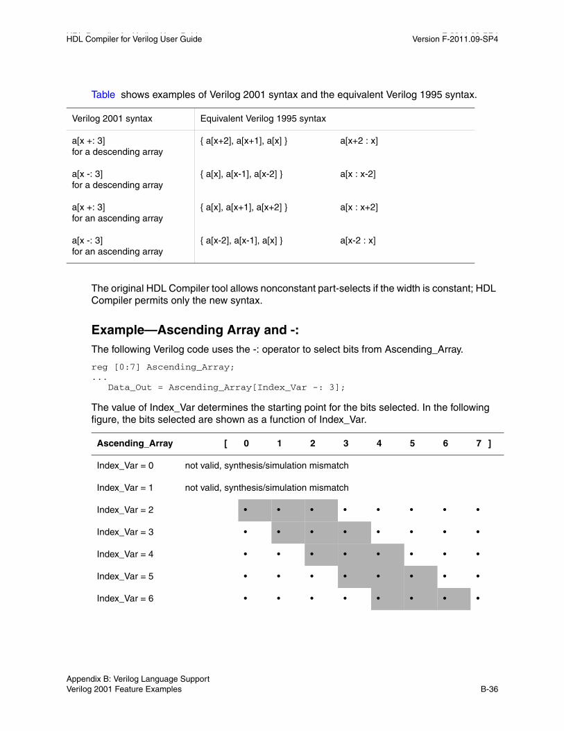
HDL Compiler for Verilog User Guide F-2011.09-SP4HDL Compiler for Verilog User Guide Version F-2011.09-SP4
Table shows examples of Verilog 2001 syntax and the equivalent Verilog 1995 syntax.
Verilog 2001 syntax Equivalent Verilog 1995 syntax
a[x +: 3] for a descending array
{ a[x+2], a[x+1], a[x] } a[x+2 : x]
a[x -: 3] for a descending array
{ a[x], a[x-1], a[x-2] } a[x : x-2]
a[x +: 3] for an ascending array
{ a[x], a[x+1], a[x+2] } a[x : x+2]
a[x -: 3] for an ascending array
{ a[x-2], a[x-1], a[x] } a[x-2 : x]
The original HDL Compiler tool allows nonconstant part-selects if the width is constant; HDL Compiler permits only the new syntax.
Example—Ascending Array and -:The following Verilog code uses the -: operator to select bits from Ascending_Array.
reg [0:7] Ascending_Array;... Data_Out = Ascending_Array[Index_Var -: 3];
The value of Index_Var determines the starting point for the bits selected. In the following figure, the bits selected are shown as a function of Index_Var.
Ascending_Array [ 0 1 2 3 4 5 6 7 ]
Index_Var = 0 not valid, synthesis/simulation mismatch
Index_Var = 1 not valid, synthesis/simulation mismatch
Index_Var = 2 • • • • • • • •
Index_Var = 3 • • • • • • • •
Index_Var = 4 • • • • • • • •
Index_Var = 5 • • • • • • • •
Index_Var = 6 • • • • • • • •
Appendix B: Verilog Language Support Verilog 2001 Feature Examples B-36

HDL Compiler for Verilog User Guide Version F-2011.09-SP4
Ascending_Array[Index_Var -: 3] is functionally equivalent to the following non-computable part-select:
Ascending_Array[Index_Var - 2 : Index_Var]
Example—Ascending Array and +:The following Verilog code uses the +: operator to select bits from Ascending_Array.
reg [0:7] Ascending_Array;... Data_Out = Ascending_Array[Index_Var +: 3];
The value of Index_Var determines the starting point for the bits selected. In the following figure, the bits selected are shown as a function of Index_Var.
Ascending_Array [ 0 1 2 3 4 5 6 7 ]
Index_Var = 0 • • • • • • • •
Index_Var = 1 • • • • • • • •
Index_Var = 2 • • • • • • • •
Index_Var = 3 • • • • • • • •
Index_Var = 4 • • • • • • • •
Index_Var = 5 • • • • • • • •
Index_Var = 6 not valid, synthesis/simulation mismatch; see the following note.
Index_Var = 7 not valid, synthesis/simulation mismatch; see the following note.
Index_Var = 7 • • • • • • • •
Ascending_Array [ 0 1 2 3 4 5 6 7 ]
Chapter B: Verilog Language Support Verilog 2001 Feature Examples B-37Appendix B: Verilog Language Support Verilog 2001 Feature Examples B-37
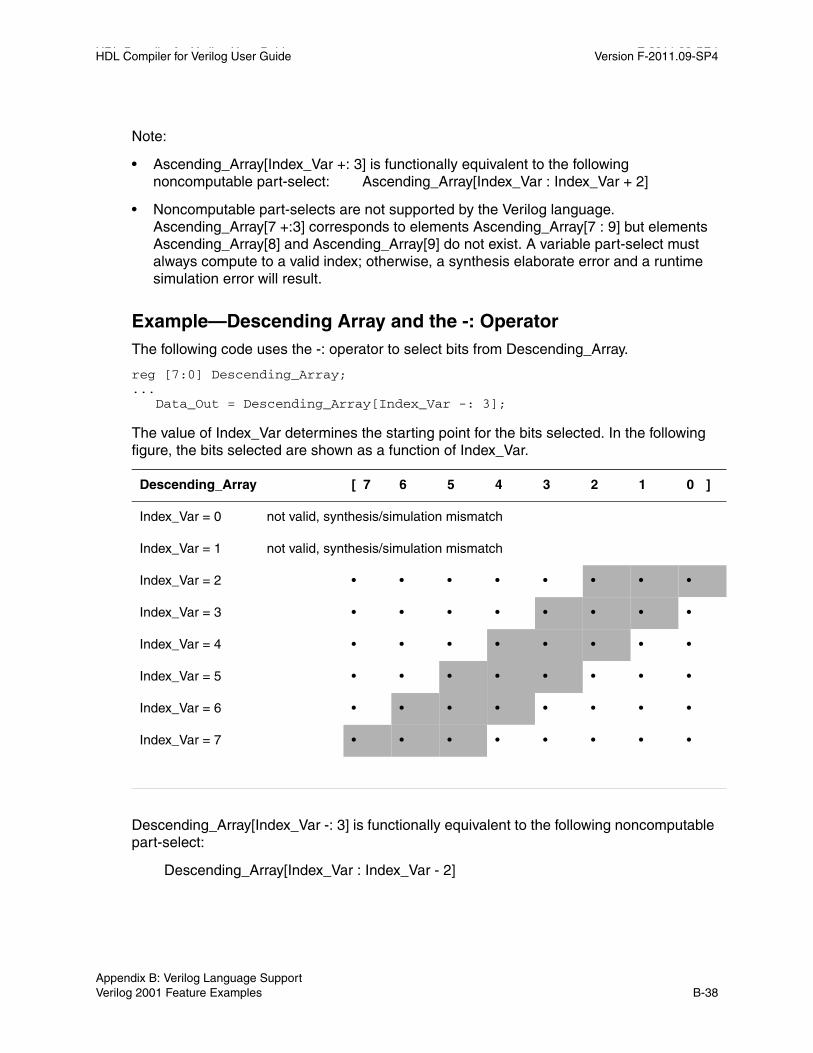
HDL Compiler for Verilog User Guide F-2011.09-SP4HDL Compiler for Verilog User Guide Version F-2011.09-SP4
Note:
• Ascending_Array[Index_Var +: 3] is functionally equivalent to the following noncomputable part-select: Ascending_Array[Index_Var : Index_Var + 2]
• Noncomputable part-selects are not supported by the Verilog language. Ascending_Array[7 +:3] corresponds to elements Ascending_Array[7 : 9] but elements Ascending_Array[8] and Ascending_Array[9] do not exist. A variable part-select must always compute to a valid index; otherwise, a synthesis elaborate error and a runtime simulation error will result.
Example—Descending Array and the -: OperatorThe following code uses the -: operator to select bits from Descending_Array.
reg [7:0] Descending_Array;... Data_Out = Descending_Array[Index_Var -: 3];
The value of Index_Var determines the starting point for the bits selected. In the following figure, the bits selected are shown as a function of Index_Var.
Descending_Array [ 7 6 5 4 3 2 1 0 ]
Index_Var = 0 not valid, synthesis/simulation mismatch
Index_Var = 1 not valid, synthesis/simulation mismatch
Index_Var = 2 • • • • • • • •
Index_Var = 3 • • • • • • • •
Index_Var = 4 • • • • • • • •
Index_Var = 5 • • • • • • • •
Index_Var = 6 • • • • • • • •
Index_Var = 7 • • • • • • • •
Descending_Array[Index_Var -: 3] is functionally equivalent to the following noncomputable part-select:
Descending_Array[Index_Var : Index_Var - 2]
Appendix B: Verilog Language Support Verilog 2001 Feature Examples B-38

HDL Compiler for Verilog User Guide Version F-2011.09-SP4
Example—Descending Array and the +: OperatorThe following Verilog code uses the +: operator to select bits from Descending_Array.
reg [7:0] Descending_Array;... Data_Out = Descending_Array[Index_Var +: 3];
The value of Index_Var determines the starting point for the bits selected. In the following figure, the bits selected are shown as a function of Index_Var.
Descending_Array [ 7 6 5 4 3 2 1 0 ]
Index_Var = 0 • • • • • • • •
Index_Var = 1 • • • • • • • •
Index_Var = 2 • • • • • • • •
Index_Var = 3 • • • • • • • •
Index_Var = 4 • • • • • • • •
Index_Var = 5 • • • • • • • •
Index_Var = 6 not valid, synthesis/simulation mismatch
Index_Var = 7 not valid, synthesis/simulation mismatch
Descending_Array[Index_Var +: 3] is functionally equivalent to the following noncomputable part-select:
Descending_Array[Index_Var + 2 : Index_Var]
Noncomputable part-selects are not supported by the Verilog language. Descending_Array[7 +:3] corresponds to elements Descending_Array[9 : 7] but elements Descending_Array[9] and Descending_Array[8] do not exist. A variable part-select must always compute to a valid index; otherwise, a synthesis elaborate error and a runtime simulation error will result.
Chapter B: Verilog Language Support Verilog 2001 Feature Examples B-39Appendix B: Verilog Language Support Verilog 2001 Feature Examples B-39

HDL Compiler for Verilog User Guide F-2011.09-SP4HDL Compiler for Verilog User Guide Version F-2011.09-SP4
Power Operator (**)
This operator performs yx, as shown in Example B-42.
Example B-42 Power Operators
module m #(parameter b=2, c=4) (a, x, y, z); input [3:0] a; output [7:0] x, y, z;
assign z = 2 ** a; assign x = a ** 2; assign y = b ** c; // where b and c are constants
endmodule
Arithmetic Shift Operators (<<< and >>>)The arithmetic shift operators allow you to shift an expression and still maintain the sign of a value, as shown in Example B-43. When the type of the result is signed, the arithmetic shift operator (>>>) shifts in the sign bit; otherwise it shifts in zeros.
Example B-43 Shift Operator Code and Gates
module s1 (A, S, Q); input signed [3:0] A; input [1:0] S; output [3:0] Q; reg [3:0] Q; always @(A or S) begin
// arithmetic shift right,// shifts in sign-bit from left
Q = A >>> S; endendmodule
Appendix B: Verilog Language Support Verilog 2001 Feature Examples B-40
HDL Compiler for Verilog User Guide Version F-2011.09-SP4
Verilog 2005 Feature Example
Zero ReplicationAccording to the Verilog 2005 LRM, a replication operation with a zero replication constant is considered to have a size of zero and is ignored. Such an operation can appear only within a concatenation in which at least one of the operands of the concatenation has a positive size.
Zero replication can be useful for parameterized designs. In the following example, the valid values for parameter P are 1 to 32.
module top #(parameter P = 32) ( input [32-1:0]a, output [32-1:0] b);assign b = {{32-P{1'b1}}, a[P-1:0]};endmodule
When hdlin_vrlg_std is set to 2005, and you analyze replication operations whose elaboration-time constant is zero or negative, the repeated expressions elaborate once (for their side-effects). But they do not contribute result values to a surrounding concatenation or assignment pattern. The Verilog 2005 standard permits such empty replication results only within an otherwise nonempty concatenation
Note: Nonstandard replication operations that are analyzed when the hdlin_vrlg_std variable is set to 1995 or 2001 return 1'b0. This is compatible with an extension made by Synopsys Verilog products of that era.
Chapter B: Verilog Language Support Verilog 2005 Feature Example B-41Appendix B: Verilog Language Support Verilog 2005 Feature Example B-41

HDL Compiler for Verilog User Guide F-2011.09-SP4HDL Compiler for Verilog User Guide Version F-2011.09-SP4
Appendix B: Verilog Language Support Verilog 2005 Feature Example B-42
Glossary GL
anonymous typeA predefined or underlying type with no name, such as universal integers.
ASIC Application-specific integrated circuit.
behavioral viewThe set of Verilog statements that describe the behavior of a design by using sequential statements. These statements are similar in expressive capability to those found in many other programming languages. See also the data flow view, sequential statement, and structural view definitions.
bit-widthThe width of a variable, signal, or expression in bits. For example, the bit-width of the constant 5 is 3 bits.
character literal Any value of type CHARACTER, in single quotation marks.
computableAny expression whose (constant) value HDL Compiler can determine during translation.
constraintsThe designer’s specification of design performance goals. Design Compiler uses constraints to direct the optimization of a design to meet area and timing goals.
convertTo change one type to another. Only integer types and subtypes are convertible, along with same-size arrays of convertible element types.
GL-1
HDL Compiler for Verilog User Guide F-2011.09-SP4HDL Compiler for Verilog User Guide Version F-2011.09-SP4
data flow viewThe set of Verilog statements that describe the behavior of a design by using concurrent statements. These descriptions are usually at the level of Boolean equations combined with other operators and function calls. See also the behavioral view and structural view.
Design CompilerThe Synopsys tool that synthesizes and optimizes ASIC designs from multiple input sources and formats.
design constraintsSee constraints.
flip-flopAn edge-sensitive memory device.
HDL Hardware Description Language.
HDL CompilerThe Synopsys Verilog synthesis product.
identifierA sequence of letters, underscores, and numbers. An identifier cannot be a Verilog reserved word, such as type or loop. An identifier must begin with a letter or an underscore.
latchA level-sensitive memory device.
netlistA network of connected components that together define a design.
optimizationThe modification of a design in an attempt to improve some performance aspect. Design Compiler optimizes designs and tries to meet specified design constraints for area and speed.
portA signal declared in the interface list of an entity.
reduction operatorAn operator that takes an array of bits and produces a single-bit result, namely the result of the operator applied to each successive pair of array elements.
registerA memory device containing one or more flip-flops or latches used to hold a value.
Glossary GL-2
HDL Compiler for Verilog User Guide Version F-2011.09-SP4
resource sharingThe assignment of a similar Verilog operation (for example, +) to a common netlist cell. Netlist cells are the resources—they are equivalent to built hardware.
RTLRegister transfer level, a set of structural and data flow statements.
sequential statementA set of Verilog statements that execute in sequence.
signalAn electrical quantity that can be used to transmit information. A signal is declared with a type and receives its value from one or more drivers. Signals are created in Verilog through either wire or reg declarations.
signed valueA value that can be positive, zero, or negative.
structural viewThe set of Verilog statements used to instantiate primitive and hierarchical components in a design. A Verilog design at the structural level is also called a netlist. See also behavioral view and data flow view.
subtypeA type declared as a constrained version of another type.
synthesisThe creation of optimized circuits from a high-level description. When Verilog is used, synthesis is a two-step process: translation from Verilog to gates by HDL Compiler and optimization of those gates for a specific ASIC library with Design Compiler.
technology libraryA library of ASIC cells available to Design Compiler during the synthesis process. A technology library can contain area, timing, and functional information on each ASIC cell.
translationThe mapping of high-level language constructs onto a lower-level form. HDL Compiler translates RTL Verilog descriptions to gates.
typeIn Verilog, the mechanism by which objects are restricted in the values they are assigned and the operations that can be applied to them.
unsignedA value that can be only positive or zero.
Chapter GL: GL-3
Glossary GL-3

HDL Compiler for Verilog User Guide F-2011.09-SP4HDL Compiler for Verilog User Guide Version F-2011.09-SP4
Glossary GL-4

Index
Symbols-: (variable part-select operator) B-35‘define B-17‘else B-19‘elsif B-19‘endif B-19‘ifdef VERILOG_1995 B-29‘ifdef VERILOG_2000 B-29‘ifdef, ‘else, ‘endif, ‘ifndef, and ‘elsif B-19‘ifndef B-19‘include B-18‘undefineall 1-18” - ” operator 3-4” + ” operator 3-4”<” operator 3-4”>” operator 3-4** (power operator) B-40+: (variable part-select operator) B-35<<< (arithmetic shift operator) B-40>>> (arithmetic shift operator) B-40$display 1-21
Aadders 2-2
carry bit overflow 3-5
carry-lookahead adder A-9mapped to synthetic library components 3-4
always blockedge expressions 2-27
always construct 1-23, 2-23, 3-30, 6-1, 6-4, B-14, B-15
arithmetic shift operators B-40Arrays of nets B-28assign 8-7assignments
always construct 1-23, 2-23, 3-30, 6-1, 6-4, B-14, B-15
blocking B-15, B-16continuous 8-6, A-3, B-28initial B-4, B-5nonblocking 1-23, B-15, B-16
Asynchronous Designs 2-24asynchronous processes 2-27
Bbinary numbers B-2bit accesses 3-26bit and memory accesses 3-26bit-blasting B-23bit-truncation
explicit 3-28
IN-1 IN-1
HDL Compiler for Verilog User Guide Version F-2011.09-SP4
bit-widthprefix for numbers B-2specifying in numbers B-2
blocking and nonblocking B-15blocking assignments B-15, B-16bus_multiple_separator_style 7-13bus_naming_style variable 1-25bus_range_separator_style 7-13Busing B-23
Ccarry-lookahead adder A-9case statements
casex,casez B-12hdlin_infer_mux 3-17, 8-3hdlin_mux_size_limit 3-17, 8-5in while loops 3-25missing assignment in a case statement
branch 3-26SELECT_OP Inference 3-13used in multiplexing logic 3-12
casex B-12casez B-12casting operators B-34coding for QoR 2-2coding guidelines 2-16coding guidelines for DC Ultra datapath
optimizationbit-truncation
implicit 3-28combinational logic 3-1Comma-separated sensitivity lists B-29compiler directives B-17conditional assignments
if-else A-17conditional inclusion of code
‘ifdef, ‘else, ‘endif, ‘ifndef, and ‘elsif Directives B-19
constant propagation 2-2
continuous assignments 8-6, A-3, B-28hdlin_prohibit_nontri_multiple_drivers 8-6
controlling signs B-34conventions for documentation xvicustomer support xvii
DD flip-flop, see flip-flopData-Path Duplication A-13dc_script_end directive 7-4, 7-5decimal numbers B-2declaration requirements
tri data type B-17deprecated features 7-20Design Compiler 1-16, 1-25, 2-24, 3-5, 5-3,
7-15, A-30directives
‘define B-17‘else B-19‘endif B-19‘include B-18‘undef B-23‘undefineall 1-18dc_script_begin 7-4dc_script_end 7-4dont_infer_multibit 7-11full_case 7-7infer_multibit 7-10, 7-11infer_mux 3-16, 7-14infer_onehot_mux 3-14, 7-14multibit inference 7-9one_cold 4-15, 7-15one_hot 7-15parallel_case 7-15parallel_case used with full_case 7-8rp_align 2-8, B-22rp_array_dir 2-8, B-21rp_endgroup 2-4, B-20rp_endignore 2-10, B-23rp_fill 2-6, B-21
IN-2 Index IN-2

HDL Compiler for Verilog User Guide Version F-2011.09-SP4
rp_group 2-4, B-20rp_ignore 2-10, B-23rp_orient 2-9, B-22rp_place 2-5, B-20see also hdlin_ for variablessimulation B-29
disable B-14don’t care 3-26don’t cares
in case statements 3-26simulation/synthesis mismatch 2-25
EELAB-302 4-14ELAB-366 6-6, 6-7elaboration errors, reporting 1-9elaboration reports 1-7embedded 3-25embedding constraints and attributes
dc_script_begin 7-4dc_script_end 7-4
enum directive 7-5enumerated type inference report 5-6enumerated types 5-6errors 1-21, 3-16, 6-2, 6-7, 7-5, 8-3, 8-6, B-5,
B-23, B-24ELAB-302 4-14ELAB-366 6-6ELAB-900 B-24
Explicit bit-truncation 3-28expression tree
optimized for delay 3-6
Ffile format, automatic detection of 1-7finite state machine 5-3
automatic detection 5-1
fsm_auto_inferring 5-3inference report 5-5
finite state machinesautomatic detection 5-1
flip 4-4flip-flop
asynchronous set and reset conditions for flip-flops 8-2, 8-4
clocked_on_also attribute A-32control register inference
hdlin_ff_always_async_set_reset 8-2hdlin_ff_always_sync_set_reset 8-2
D-flip-flopD flip-flop with a synchronous load and an
asynchronous load 4-20D flip-flop with an asynchronous reset 4-19D flip-flop with an asynchronous set 4-18D flip-flop with synchronous reset 4-20D flip-flop with synchronous set A-35rising-edge-triggered D flip-flop 4-18
hdlin_ff_always_async_set_reset 8-2, 8-4hdlin_ff_always_sync_set_reset 8-2master-slave latches A-32SEQGENs 4-2synchronous set and reset conditions for flip-
flops 8-2used to describe the master-slave latch A-32
flowsinteracting with low-power flows 2-19interacting with other flows 2-18interacting with Synthesis flows 2-18interacting with verification flows 2-22
for loop 3-31FSM inference variables 5-3fsm_auto_inferring 5-3full_case 7-7functional description
function declarations in 1-23functions 1-25, 2-27, 5-2, 6-2, 7-5, B-3, B-18,
B-29, B-31, GL-2
IN-3 Index IN-3
HDL Compiler for Verilog User Guide Version F-2011.09-SP4
Ggate-level constructs 1-23
Hhdlin_check_no_latch 8-2hdlin_elab_errors_deep 1-9hdlin_ff_always_async_set_reset 8-2, 8-4hdlin_ff_always_async_set_reset directive 8-2hdlin_ff_always_sync_set_reset 8-2hdlin_infer_function_local _latches 8-2hdlin_infer_mux 3-17, 8-3hdlin_keep_signal_name variable 2-19hdlin_module_arch_name_split 8-4hdlin_mux_oversize_ratio 3-17, 8-4hdlin_mux_size_limit 3-17, 8-5hdlin_mux_size_min 3-17, 8-5hdlin_mux_size_only variable 3-18hdlin_preserve_sequential variable 4-9, 8-6hdlin_prohibit_nontri_multiple _drivers 8-6hdlin_prohibit_nontri_multiple_drivers 6-6hdlin_reporting_level directive 5-3hdlin_reporting_level variable 1-7, 4-5, 6-2hdlin_subprogram_default_values 8-6hdlin_upcase_names 8-7hdlin_vrlg_std 1-7hexadecimal numbers B-2hierarchical
boundaries 1-25constructs 1-23
IIf 4-4if statements
hdlin_infer_mux 3-17, 8-3in case statements 3-26infer MUX_OP cells 3-16
ifdef VERILOG_1995 B-29
ifdef VERILOG_2001 B-29if-else A-17ignored functions B-29implicit bit-truncation 3-28include B-18incompletely specified case statement 3-26infer_multibit 7-10infer_mux 3-16infer_mux directive 7-14infer_onehot_mux directive 3-14, 7-14inference report
description 6-2inference reports 4-5
enumerated types 5-6finite state machine 5-5multibit components 7-12
inferring flip-flops 4-16initial assignment B-4, B-5inout
connecting to gate B-16connecting to module B-16
instantiations 1-23, 1-25, 6-6, 8-7, 8-8, A-27, A-28, A-29, B-16
Llatches
avoiding unintended latches 3-30clocked_on_also A-32D latch 4-14D latch with an active-low asynchronous set
and reset 4-15generic sequential cells (SEQGENs) 4-2master-slave latches A-32resulting from conditionally assigned
variables 4-14SR latches A-30
late-arriving signals A-13datapath duplication solution A-13
IN-4 Index IN-4

HDL Compiler for Verilog User Guide Version F-2011.09-SP4
moving late-arriving signal close to output solution A-13
lexical conventions B-2license requirements 1-30loops
case statementsin while loops 3-25
Mmacro substitution B-17macromodule B-16macros B-20
global reset‘undefineall 1-18
local reset‘undefineall B-23
macro definition on the command line B-18specifying macros
‘define B-17specifying macros that take arguments B-17SYNTHESIS 1-18VERILOG_1995 1-18VERILOG_2001 1-18
memory accesses 3-26mismatch 6-2
full_case usage 7-7parallel_case usage 7-15simulator/synthesis 6-2three-states 2-23, 6-4z value 6-2z value comparison 6-2
moduleconnecting to inout B-16
multibit componentsbenefits 6-1bus_multiple_separator_style 7-13bus_range_separator_style 7-13described 6-1multibit inference report 7-12report_multibit command 7-12
multibit inference directives 7-9multidimensional arrays B-30multiplexer
cell size 3-21MUX_OP 3-20
multiplexers 3-26multiplexing logic
case statements embedded in if-then-else statements 3-25
case statements in while loops 3-25case statements that contain don’t care
values 3-26case statements that have a missing case
statement branch 3-26Design Compiler implementation 3-14for bit or memory accesses 3-26hdlin_infer_mux variable 3-16hdlin_mux_oversize_ ratio 3-17hdlin_mux_size_limit 3-17, 8-5hdlin_mux_size_min 3-17if-else-begin-if constructs A-17implement conditional operations implied by
if and case statements 3-13incompletely specified case statement 3-26infer MUX_OP cells 3-15infer_mux 3-16MUX_OP cells 3-12MUX_OP Inference Limitations 3-25preferentially map multiplexing logic to
multiplexers 3-12SELECT_OP cells 3-12sequential if statements A-16warning message 3-26with if and case statements 3-12
MUX_OP cells, setting the size_only attribute 3-18
MUX_OP inference 3-15
Nnonblocking assignments 1-23, B-15, B-16number
IN-5 Index IN-5

HDL Compiler for Verilog User Guide Version F-2011.09-SP4
binary B-2decimal B-2formats B-2hexadecimal B-2octal B-2specifying bit-width B-2
Ooctal numbers B-2one 7-15one_cold directive 4-15, 7-15one_hot directive 7-15one-hot multiplexer 3-14operators
casting B-34power B-40shift B-40variable part-select B-35
optimization 5-1fsm_auto_inferring 5-3
Pparallel_case 7-7, 7-15parameterized design 1-19parameters 1-17, 1-19, 1-21, 2-2, 7-5, 7-19,
B-4, B-28Part-Select Addressing B-35ports
inout port requirements B-16Power B-40power operator (**) B-40processes
asynchronous 2-27synchronous 2-27
Rradices B-2
read_file -format command 1-7reading designs
analyze -f verilog { files } elaborate 1-17automatic structure detector 1-16netlists 1-16parameterized designs 1-16read -f verilog -netlist { files } (dcsh) 1-17read_file -f verilog -netlist { files } (tcl) 1-17read_file -f verilog -rtl { files } 1-17read_verilog 1-17read_verilog -netlist { files } (tcl) 1-17read_verilog -rtl { files } (tcl) 1-17RTL 1-16
register inferencevariables that control inference 8-2
register inference examples 4-14relative placement 2-2
compiler directives 2-4, B-17creating groups 2-4, B-20examples 2-10figures 2-12ignoring 2-10, B-23placing cells automatically 2-6, B-21specifying cell alignment 2-8, B-22specifying cell orientation 2-9, B-22specifying placement 2-8, B-21specifying subgroups, keepouts, and
instances 2-5, B-20remove_design 1-17removing designs 1-17report_multibit 7-12report_multibit command 7-12resets
global reset‘undefineall 1-18
local reset‘undef B-23
SSELECT_OP 3-13
IN-6 Index IN-6
HDL Compiler for Verilog User Guide Version F-2011.09-SP4
sensitivity list 2-26Sequential if statements A-16set and reset conditions for flip-flops 8-2, 8-4shift operators B-40Sign Conversion Warnings 3-7sign rules B-33signal names, keeping 2-19signed arithmetic extensions B-31Signed Constants B-32Signed I/O Ports B-31signed keyword B-33Signed Registers B-32Signed Types B-32signs
casting operator B-34controlling signs B-34sign conversion warnings B-34
simulationdirectives B-29
simulator/synthesis mismatchfull_case usage 7-7parallel_case usage 7-15
slow reads 1-16SolvNet
accessing xviidocumentation xiv
standard macrosmacro definition on the command line B-18see also macrosSYNTHESIS 1-18VERILOG_1995 1-18VERILOG_2001 1-18
structural descriptionelements of 1-23
synchronousprocesses 2-27
SYNTHESIS macro B-27synthetic comments.See directivessystem functions, Verilog B-29
Ttasks 1-21, 1-23, 1-25, 2-26, 2-27, 5-2, 8-2,
B-3, B-4, B-14template
directive 7-19See also parameterized designs
three-state bufferhdlin_prohibit_nontri_multiple_drivers 6-6tri data type B-17
tri Data Type declaration requirement B-17two-phase design A-34
Uunloaded registers, keeping 4-9
Vvariable
conditionally assigned 4-14reading 4-14
variable part-select operators B-35variables, (see hdlin_)VER 3-7VER-318 3-7, 3-8, 3-9, 3-11, 3-12Verilog
keywords B-3system function B-29
Verilog 2001 features B-27‘ifndef, ‘elsif, ‘undef B-28ANSI-C-style port declaration B-28arithmetic shift operators B-28casting operators B-28comma-separated sensitivity lists B-29disabling features 1-18hdlin_vrlg_std = 1995 1-18hdlin_vrlg_std = 2001 1-18implicit event expression list B-28multidimensional arrays B-28parameter passing by name B-28power operator (**) B-28
IN-7 Index IN-7

HDL Compiler for Verilog User Guide Version F-2011.09-SP4
signed/unsigned nets and registers B-28signed/unsigned parameters B-28signed/unsigned sized and based constants
B-28sized parameters B-28SYNTHESIS macro B-27
Verilog language version, controlling 1-7verilogout_ variables 8-7verilogout_no_tri variable 8-8vrlg_std 8-7
Wwarnings
asynchronous designs 2-24encodings 7-6hdlin_unsigned_integers B-33sign conversion 3-8VER-318 3-8
while loop B-24, B-25, B-26, B-27
IN-8 Index IN-8
Recommended