Embed Size (px)
Citation preview

(12) United States Patent USOO6289434B1
(10) Patent No.: US 6,289,434 B1 Roy (45) Date of Patent: *Sep. 11, 2001
(54) APPARATUS AND METHOD OF (56) References Cited IMPLEMENTING SYSTEMS ON SLICON U.S. PATENT DOCUMENTS USING DYNAMIC-ADAPTIVE RUN-TIME RECONFIGURABLE CIRCUITS FOR 5,517,436 5/1996 Andreas ............................... 364/736 PROCESSING MULTIPLE, INDEPENDENT 5,652,903 * 7/1997 Weng ..................................... 712/35 DATA AND CONTROL STREAMS OF 55. : 5. I - - - - - - - - 223:
2 a? a upp ..... - - - -
WARYING RATES 5,822,606 * 10/1998 Morton. ... 712/16 5,933,624 * 8/1999 Balmer. ... 709/400
(75) Inventor: Rupan Roy, Fremont, CA (US) 5,956,518 * 9/1999 Detlon ... ... 712/15 6,049,859 4/2000 Gliese .................................... T12/17 (73) Assignee: Cognigine Corporation, Fremont, CA f eSe f
(US) * cited by examiner Primary Examiner Eric Coleman
(*) Notice: This patent issued on a continued pros ecution application filed under 37 CFR (57) ABSTRACT 1.53(d), and is subject to th 'yny An apparatus and method processes data in Series or in patent term provisions o a a- - parallel. Each of the processorS operating may perform 154(a)(2). arithmetic-type functions, logic functions and bit manipula Subiect to anv disclaimer, the term of this tion functions. The processors can operate under control of at is Nended or adiusted under 35 a Stored program, which configures each processor before or S.C. 154(b) by Oda during operation of the apparatus and method to perform a
a -- y yS. Specific function or Set of functions. The configuration of each processor allows each individual processor to optimize
(21) Appl. No.: 09/032,530 itself to perform the function or functions as directed by the (22) Filed: Feb. 27, 1998 Stored program, while providing maximum flexibility of the
apparatus to perform any function according to the needs of Related U.S. Application Data the Stored program or other stored programs. Communica
(60) Provisional application No. 60/039.237, filed on Feb. 28, tion between processors is facilitated for example, via a 1997. memory under control of memory management. Communi
7 cation between the processors and external devices is facili - - - - - - - - - - - - - - - - - - - - - - - - - - - - - - - - - - - 712,32.71 sets tated by the memory management and units capable of
S. Fi la fs - - - - - - - - h - - - - - - - - - - - - - - - - - - - - - s 65,800 f 1. 7. 4 performing Specialized or general interface functions. e O SeaC. ......................... ll s
712/32, 22, 21, 9; 709/221; 713/100 1 Claim, 64 Drawing Sheets
SRAM MEDIA PROCESSING ONr. SGRAM : 96 OCA | DATA RAM H - MEDIA ||
BUFFER ;INSTR. CACHE 9. Processor E. MEDIA PROCESSING UNIT
s DATARAM 495 Media PEP- NSR. CACHE 9.64 PROCESSOR :
! PROCES- | MEDIA PROCESSING UNIT 5. DATA RAM - MEDIA:
h LocAL INTER-NsTR. AcHE 64 PROCESSOR: : as EMPU . INTER- ROU- EMEDIA PROCESSING UNIT 32 Act TER : 9 eEEp. As a P". SEG
A video : cMM : INSTR. CACHEH CAPTURE CA. MEDIA PROCESSING UNIT
w
1s, 'S SS DATARAM 9. MEDA NTSC, TROL- INSTR. CACHE 64, PRocessor
al S." MEDIA PROCESSING UNIT : OUT : DATA RAM - MEDIA: AUDIOl. "NstroAcHE: 64, PROCESSOR: "EE". MEDIA PROCESSING UNIT
16. E. DATARAM 98 - MEDIA : It is INSTR, CACHE 64, PROCESSOR:
l
EVEN ---MEDIA PROCESSING UNIT TIMER DATA RAM - MEDIA: ON-CHP Memori INSTR, CACHE 64, PROCESSOR |

U.S. Patent Sep. 11, 2001 Sheet 1 of 64 US 6,289,434 B1
CLOCK
MEMORY
A/G 7

U.S. Patent Sep. 11, 2001 Sheet 2 of 64 US 6,289,434 B1
CLOCK
COMPUTE COMPUTECOMPUTECOMPUTE CONFIG ELEMENTELEMENTELEMENT URATION
SEOUENCE
1
S4N s2(NSs2Ye Sas Sassee3. ERG a2 esa St.
PIPE STAGEN-2
N V NNM NNM NM NM NM MICRO
is a Eis E. S. A. K. K. SEQUENCE PIPE STAGE N+3 K
A/G 2

U.S. Patent Sep. 11, 2001 Sheet 3 of 64 US 6,289,434 B1
MEDIA PROCESSING UNITTTTT
- DATA RAM 9 64 LINSTR, CACHEH
MEDIA PROCESSING UNIT 96 64. DATA RAM
;INSTR. CACHE MEDIA PROCESSING UNIT,
SDRAM/ SGRAM LOCAL BUFFER INTER FACE
ERAL PROCES- y
SING : : 96
INSTR. CACHE MEDIA PROCESSING UNIT
96 AND 64 DATA RAM 64
(LINSTR. CACHEH i MEDIA PROCESSING UNIT l
DATA RAM 9 N: 64 {INSTR. CACHEH
--------------------------- MEDIA PROCESSING UNIT -
| DATARAM 98 64 64
INSTR. CACHEH I MEDIA PROCESSING UNIT
6 4. DATA RAM 498 i 64
|INSTR. CACHEH ----------------ee-s-s-s-s-runs are---------------------
MEDIA PROCESSING UNIT
DATARAM 96 A/G 3 64
ON-cHIP MEMoRY INSTR. CACHE re- - - - - - - - - - - - - - - - - - - - - - - - -
CAPTURE
FACE INTER

U.S. Patent Sep. 11, 2001 Sheet 4 of 64 US 6,289,434 B1
32 MB OFF-CHIP MEMORY SPACE
Ox38OOOOO
Ox3OOOOOO 0x2FFFFFF 16 MBYTE LOCAL BUFFER
OX18OOOOO Ox17FFFFF MEDIA PROCESSING
Ox16FFFFF MEDIA PROCESSING
Ox15OOOOO UNIT #5 (MPU5) Ox14FFFFF MEDIA PROCESSING OX14OOOOO UNIT #4 (MPU4)
MEDIA PROCESSING OX13OOOOO UNIT #3 (MPU3) 0x12FFFFF MEDIA PROCESSING
Ox11FFFFF MEDIA PROCESSING
OX1 OOOOOO UNIT #0 (MPUO)
0x08OOOOO Ox07FFFFF
0x06OOOOO Ox05FFFFF AUXLIARY SERAL PARALLEL
0x04FFFFF
A/G. 44
16 MB ON-CHP MEMORY SPACE

U.S. Patent Sep. 11, 2001 Sheet S of 64 US 6,289,434 B1
0x03FFFFF OxO3OOOOO LOCAL MEMORY INTERFACE (LMI) 0x02FFFFF PERIPHERAL COMPONENT 16 MB OxO2OOOOO INTERCONNECT (PCI) ON-CHIP
1 MEMORY MANAGEMENT UNIT (MMU) ERY OXO1 OOOOO
OxOOFFFFF GLOBAL REGISTERS OxOOOOOOO
A/G 4A
A/G 4

U.S. Patent Sep. 11, 2001 Sheet 6 of 64 US 6,289,434 B1
31 30 29 28 24 23 O rw acc. b.cnt. 24 BitTransfer Dword Address
rW : read/write, O = read transfer, 1 F write transfer 3CC : access priority, 00F lowest, 11 = highest b. Cnt. : burst count - 1, 00000 = 1 Dword 11111 = 32 Dwords
A/G 4O
REQ-OUT
DATA-OUT 3 (ADDRESS)
ROY-IN
DATA-IN (DATA)
A/G 6

U.S. Patent Sep. 11, 2001 Sheet 7 of 64 US 6,289,434 B1
CLK
It is bó
n- On+2 On 3
REO-OUT
DATA-OUT (ADDRESS)
RDY-IN
DATA-IN 3% (DATA) 2

U.S. Patent Sep. 11, 2001 Sheet 8 of 64 US 6,289,434 B1
REO-OUT
DATA-OUT (ADDRESS2 & DATA) 4
RDY-IN
A/G 7

U.S. Patent Sep. 11, 2001 Sheet 9 of 64 US 6,289,434 B1
RECQ-OUT
DATA-OUT (ADDRESS3 & DATA) 22 ) On 4
A/G 3

U.S. Patent Sep. 11, 2001 Sheet 10 of 64 US 6,289,434 B1
111111111111111100001111 OOOOOO11
ZERO FILL
111111111111100001111 OOOOOO1 1000
A/G 9
11111111111111110000111100000011
ZERO FILL

U.S. Patent Sep. 11, 2001 Sheet 11 of 64 US 6,289,434 B1
I OOOO111100111100 1111 OOOO11 OOOO11
ZERO FILL
OOOOOOOOOOOOOOOOO1111001111 OOOOO
ZERO FILL
OOOOOOOOOOOOO1111000011000011000
A/G 72
OOOO111100111100 1111000011000011
ZERO FILL
OOOOOOOOOOOOO1111000011000011000
A/G 73
0000111100111100 1111 OOOO11 OOOO11
ZERO FILL
OOOOOOOOOOOOOOOOO111100111100000
A/G 74
11110101 11110101 11110101 11110101
ZERO FILL OOOOOOOOOOOOOOOOOOOOO11110101000
A/G 76
U.S. Patent Sep. 11, 2001 Sheet 12 of 64 US 6,289,434 B1
11110101 11110101 11110101 11110101
ZERO FILL
OOOOOOOOOOOOOOOOOOOOO11110101 OOO
ZERO FILL
OOOOOOOOOOOOOOOOOOOOO11110101000
A/G 76
11110101 11110101 11110101 11110101
OOOOOOOOOOOOOOOOOOOOO11110101000
ZERO FILL ZERO FILL
OOOOOOOOOOOOOOOOOOOOO11110101000
A/G 77
1111000011000011 1111 OOOO11 OOOO11
ZERO FILL 1000011000011000 1000011000011000
A/G 73

U.S. Patent Sep. 11, 2001 Sheet 13 of 64 US 6,289,434 B1
------, -------------
1111000011000011 1111000011000011
000001 1:OOOOOOOOO 0000011000000000
H...----.
1111000011000011 1111000011000011
dd0001 ddddddddd | did0001 ddddddddd
11110101 11110101 11110101 11110101
ZERO FILL OOOOO11110101OOO OOOOO11110101000
A/G 27

U.S. Patent Sep. 11, 2001 Sheet 14 of 64 US 6,289,434 B1
11110101 11110101 11110101 11110101
OOOOO111101 01 000 OOOOO11110101000
ZERO FILL ZERO FILL
OOOOO11110101000 OOOOO11110101000
A/G 22
11110101 11110101 11110101 11110101
10101000 10101000 10101000 10101000
ZERO FILL
A/G 23
11110101 11110101 11110101 11110101
000000 0000000 O0100000 00100000 O
A/G 24

U.S. Patent Sep. 11, 2001 Sheet 15 of 64 US 6,289,434 B1
11110101| 11110101 11110101 11110101
doiddddd do1ddddd | doiddddd | doiddddd A/G 26
1111 OOOO11000011 1111000011000011
10101000 10101000 10000110 10000110
A/G 26
OOO1000011000011 1111000011000011
10101000 10101000 10000110
A/G 27
11111111

U.S. Patent Sep. 11, 2001 Sheet 16 of 64 US 6,289,434 B1
111111111111111100001111 OOOOOO11
ZERO FILL
1111111111111 OOOO1111 OOOOOO11 OOO
A/G 23
ZERO FILL
A/G 30

U.S. Patent Sep. 11, 2001 Sheet 17 of 64 US 6,289,434 B1
I OOOO111100111100 1111 OOOO11000011
SIGNEXT.
OOOOOOOOOOOOOOOOO1111 OO11 11 OOOOO
SGN EXT.
11111111111111111 OOOO11 OOOO11000
A/G 37
OOOO111100111100
SIGNEXT.
11111111111111111 OOOO11000011000
A/G 32
1111 OOOO1 1000011
0000111100111100 1111 OOOO1 1000011
OOOOOOOOOOOOOOOOO111 1 001111 OOOOO
SIGNEXT.
A/G 33
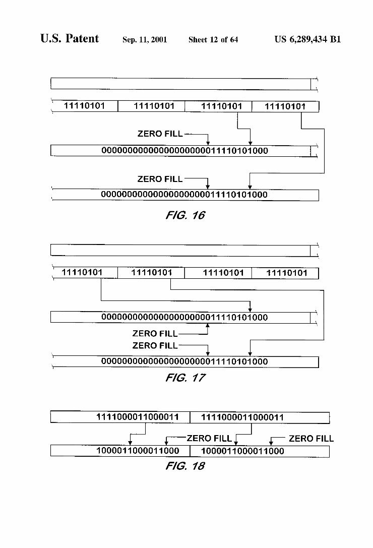
U.S. Patent Sep. 11, 2001 Sheet 18 of 64 US 6,289,434 B1
S1110101 S1110101 S1110101 S1110101
SIGN EXTEND
SSSSSSSSSSSSSSSSSSSSSS11 1 01 01 000
A/G 34
O1110101 11110101 11110101 O1110101
SIGNEXTEND
11111111111111111111111110101000
SIGN EXTEND
OOOOOOOOOOOOOOOOOOOOOO1110101000
A/G. 36
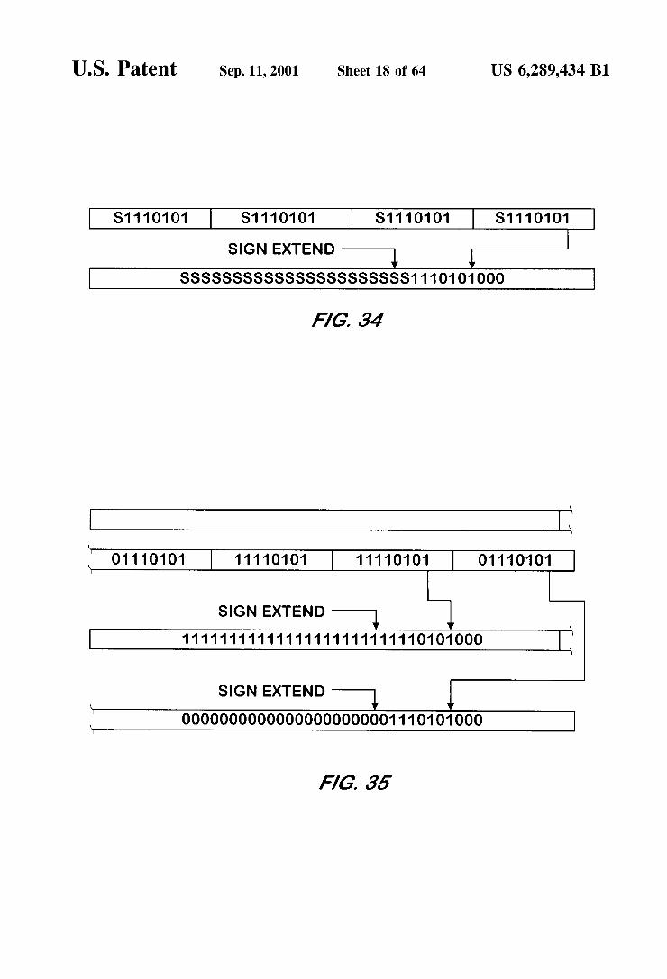
U.S. Patent Sep. 11, 2001 Sheet 19 of 64 US 6,289,434 B1
O1110101 11110101 11110101 O1110101
OOOOOOOOOOOOOOOOOOOOOO1110101 OOO
SIGN EXTEND
11111111111111111111111110101 OOO
SIGNEXTEND
A/G. 36
1111000011000011 1111000011000011
ZERO FILL
1 OOOO1 1000011000 1OOOO11 OOOO11 OOO
ZERO FILL
A/G 37
U.S. Patent Sep. 11, 2001 Sheet 20 of 64 US 6,289,434 B1
S111 OOOO11:OOOO11 S111000011000011
1111000011000011 1111000011000011
- dd00011ddddddddd do)0011ddddddddd
S1110101 S1110101 S1110101 S1110101
SSSSSS1110101 OOO
SIGNEXT.
SSSSSS11 1 01 01000
SIGNEXT.
A/G 40

U.S. Patent Sep. 11, 2001 Sheet 21 of 64 US 6,289,434 B1
O1110101 11110101 11110101 O1110101
SIGNEXT.
OOOOOO1110101000 1111111110101000
1111111110101000 OOOOOO1110101000
A/G 47
11110101 11110101 11110101 11110101
10101000 10101000 10101000 10101000
ZERO FILL
A/G 42
S1110101 S1110101 S1110101 S1110101
S0-100000 SO1:00000 SO100000 SO100000
A/G 43

U.S. Patent Sep. 11, 2001 Sheet 22 of 64 US 6,289,434 B1
11110101 11110101 11110101 11110101
doiddddd dO1ddddd dO1ddddd dO1ddddd
A/G 44
1111111111111111 OOOO1111 OOOOOO11
ZERO FILL OOO1111111111111111 OOOO1111 OOOOO

U.S. Patent Sep. 11, 2001 Sheet 23 of 64 US 6,289,434 B1
OOOO111 1 00111100 1111 OOOO11 OOOO11
OOOOOOOOOOOOOOOOOOOOOOO111100111
ZERO FILL
OOOOOOOOOOOOOOOOOOO1111000011000
ZERO FILL
A/G 49
0000111100111100 111 1 000011 OOOO11
ZERO FILL
OOOOOOOOOOOOOOOOOOO1111 OOOO11 OOO
A/G. 49
0000111100111100 1111 OOOO11 OOOO11
OOOOOOOOOOOOOOOOOOOOOOO111100111
ZERO FILL
A/G 60
U.S. Patent Sep. 11, 2001 Sheet 24 of 64 US 6,289,434 B1
11110101 11110101 11110101 11110101
ZERO FILL
OOOOOOOOOOOOOOOOOOOOOOOOOOO11110
A/G 37
11110101 11110101 11110101 11110101
OOOOOOOOOOOOOOOOOOOOOOOOOOO11110
ZERO FILL
OOOOOOOOOOOOOOOOOOOOOOOOOOO11110
ZERO FILL
A/G 62

U.S. Patent Sep. 11, 2001 Sheet 25 of 64 US 6,289,434 B1
11110101 11110101 11110101 11110101
OOOOOOOOOOOOOOOOOOOOOOOOOOO11110
ZERO FILL
OOOOOOOOOOOOOOOOOOOOOOOOOOO11110
ZERO FILL
A/G 63
1111 OOOO11 OOOO11 1111 OOOO11 OOOO11
OOO1111 OOOO11 OOO 0001111000011000
ZERO FILL ZERO FILL
A/G. 64
11100001:1000011 1111000011000011
00000 1000010000 0000011000010000 ZERO FILL
1
ZERO FILL
A/G 66

U.S. Patent Sep. 11, 2001 Sheet 26 of 64 US 6,289,434 B1
11:11000011000011 1111000011000011
ddddd 100001:dddd ddddd1100001dddd
11110101 11110101 11110101 11110101
OOOOOOOOOOO11110 OOOOOOOOOOO11110
ZERO FILL ZERO FILL
A/G 67
I 11110101 11110101 11110101 11110101
OOOOOOOOOOO11110
ZERO FILL
OOOOOOOOOOO11110
ZERO FILL
OOOOOOOOOOO11110 OOOOOOOOOOO11110
A/G 63

U.S. Patent Sep. 11, 2001 Sheet 27 of 64 US 6,289,434 B1
11110101 11110101 11110101 11110101
ZERO FILL
11110101 11110101 11110101 11110101
00001100 OOOO11:00 OOOO11:00 00001100 ZERO FILL
U.S. Patent Sep. 11, 2001 Sheet 28 of 64 US 6,289,434 B1
11110101 11110101 11110101 11110101
ddd11dd dddd11dd dddd11dd dddd11dd
A/G 67
S111111111111111 OOOO1111 OOOOOO11
SIGN EXTEND
SSS111111111111111100001111 OOOOO
A/G 62

U.S. Patent Sep. 11, 2001 Sheet 29 of 64 US 6,289,434 B1
OOOO111100111100 1111 OOOO11 OOOO11
OOOOOOOOOOOOOOOOOOOOOOO111100111
SIGNEXTEND
11111111111111111111111000011000
SIGN EXTEND
A/G 66
OOOO111 1 001111 OO 1111 OOOO11 OOOO11
11111111111111111111111 OOOO11 OOO
SIGN EXTEND
A/G. 66

U.S. Patent Sep. 11, 2001 Sheet 30 of 64 US 6,289,434 B1
OOOO111100111100 1111 OOOO11 OOOO11
OOOOOOOOOOOOOOOOOOOOOOO111100111
SIGN EXTEND
A/G 67
OOOO111 1 00111100 1111 OOOO11 OOOO11
OOOOOOOOOOOOOOOOOOOO111100111100
SIGN EXTEND
A/G 63
OOOO111 1 00111100 1111 OOOO11 OOOO11
OOOOOOOOOOOOOOOOOOOO111100111100
SIGN EXTEND
A/G 69

U.S. Patent Sep. 11, 2001 Sheet 31 of 64 US 6,289,434 B1
S1110101 S1110101 S1110101 S1110101
SSSSSSSSSSSSSSSSSSSSSSSSSSSS1110
SIGN EXTEND
A/G 70
O1110101 11110101 11110101 O1110101
11111111111111111111111111111110
SIGN EXTEND
OOOOOOOOOOOOOOOOOOOOOOOOOOO11110
SIGN EXTEND
A/G 77
U.S. Patent Sep. 11, 2001 Sheet 32 of 64 US 6,289,434 B1
11110101 11110101 11110101 11110101
OOOOOOOOOOOOOOOOOOOOOOOOOOO11110
SIGN EXTEND
11111111111111111111111111111110
SIGNEXTEND
A/G 72
S11 1000011000011 S11 1 000011 OOOO11
SIGN EXTEND
SSSS111000011000 SSSS111 OOOO11 OOO
A/G 73

U.S. Patent Sep. 11, 2001 Sheet 33 of 64 US 6,289,434 B1
111000011000011 1111000011000011
sssss 100000000 SSSSS11000010000 SIGN EXTEND
1
SIGN EXTEND
A/G 74
11:1100001:1000011 11:1100001:1000011
ddddd11 00001:dddd ddddd1100001:dddd
A/G. 75
S1110101 S1110101 S1110101 S1110101
SSSSSSSSSSS11110 SSSSSSSSSSS11110
SIGN EXTEND SIGNEXTEND
A/G 76
U.S. Patent Sep. 11, 2001 Sheet 34 of 64 US 6,289,434 B1
11110101 01110101 11110101 O1110101
1111111111111110 OOOOOOOOOOO11110
SIGNEXT SIGNEXT.
1111111111111110 OOOOOOOOOOO11110
A/G 77
S1110101 S1110101 S1110101 S1110101
1110101 1110101 1110101 1110101
dddd11dd dadd 1dd diddd 1dd dddd11dd

U.S. Patent Sep. 11, 2001 Sheet 35 of 64 US 6,289,434 B1
O1 OO11111111111100001111 OOOOOO11
O111111111111 OOOO1111 OOOOOO11010
A/G 31
01 01000011000011 O1 01000011000011
1000011000011010 1000011000011010
A/G 32
11010101 11010101 11010101 11010101
E. E. E. E. 10101110 10101110 10101110 10101110
O10011111111111100001111 OOOOOO11
O110100111111111111 OOOO1111 OOOOO
A/G 34

U.S. Patent Sep. 11, 2001 Sheet 36 of 64 US 6,289,434 B1
01 01000011000011 01 01000011000011
O1 1 01 01 OOOO11 OOO O1101 O1 OOOO11 OOO
10111010 10111010 10111010 10111010
A/G 36 64. BITS 64. BITS 64. BITS 64. BITS -HD -HD
DOUBLE DOUBLE DOUBLE DOUBLE QWORDSQWORDSQWORDSQWORDS
TWO INSTRUCTIONS PROGRAM COUNTER
A/G 37

U.S. Patent Sep. 11, 2001 Sheet 37 of 64 US 6,289,434 B1
Quad Port Ram Single Port Ram 64 x 32 bits 256 x 32 bits
Data Address Data-in Data-Out in Out Address
EHEH!" H-H Data
||EEE) put | \ E. | | | | S '', Data
HET ... I
\ N N N |
Quad Port Single Port Cache
A/G 33
33 2 2 221111111111 7 1 10 7 4. 109876543.210
El LLLVIZNCVIZINC C m SSSSaalaammimim P VV BBBB
A/G. 394

U.S. Patent
Bi t S
15
17-16 :
18
19
: EmV
AP
: ICP
: US
Sep. 11, 2001 Sheet 38 of 64 US 6,289,434 B1
- Carry flag of the MAU - Negative flag of the MAU - Zero flag of the MAU - Overflow flag of the MAU - Carry flag of the ALU - Negative flag of the ALU - Zero flag of the ALU - Overflow flag of the ALU - Bit O of the BMU result - Bit 8 of the BMU result - Bit 16 of the BMU result - Bit 24 of the BMU result - Sleep bit.
O = Puts MPU into sleep mode 1 = Puts MPU in normal operation mode (wake)
- Internal move bit. O = No MPU initiated move in progress 1 = MPU initiated move in progress, MPUDMA
busy - External move bit.
O = No externally initiated move to/from MPU in progress
1 = Externally initiated move to/from MPU in progress
- Access Priority for MPU (set by supervisor). 00 = lowest priority 11 = highest priority
- instruction Cache Pre-fetch. O = No prefetch 1 F Pre-fetch the next instuction cache block
- Userl'Supervisor bit. 0 = User, 1 = Supervisor
A/G. 394 A/G. 39A
A/G 39As A/G. 39

U.S. Patent Sep. 11, 2001 Sheet 39 0f 64 US 6,289,434 B1
31 28 27 24 23 20 19 16 15 12 11 8 7 4 3 O
ALU Carry, Negative, Zero and MAU Carry, Negative, Zero and Overflow Overflow
A/G 90
33 222 222 22 22 1 1 1 1 1 1 1 1 1 1 9 8 7 6 5 4 3 2 1 0 10 9 8 7 6 5 4 3 2 1 0 9 8 7 6 5 4 3 2 1 0
TSVVH TSVVHP
Reserved FFFF Reserved EEEEC D D F E E
Interrupt Flags Interrupt Mask and Control
A/G 974

U.S. Patent
1
13-6
14
15
16
17
18
: PCE
: HE
: VE
: WIDE
: SE
: TE
: Reserved
: ES
: EU
: PCF
: HF
: VF
Sep. 11, 2001
- PCI Interrupt Enable (from PC) OF Disable 1 F Enable
1 F Enable - Vsync interrupt Enable (from CDI)
OF Disable 1 F Enable
1 F Enable - Software Interrupt Enable
OF Disable 1F Enable
- Timer Interrupt Enable 0 F Disable 1 F Enable
- Enable Supervisor interrupts O = Disable 1 F Enable
- Enable User Interrupts. OF Disable 1 = Enable
- PCI Interrupt Flag O = No interrupt 1 = Interrupt
- Hsync interrupt Flag O = No interrupt 1 = Interrupt
- Vsync interrupt Flag 0 = No interrupt 1 = Interrupt
A/G 97A
Sheet 40 of 64 US 6,289.434 B1
- Hsync interrupt Enable (from CD) O = Disable
- Video Capture Data Available Enable (from VCI) O = Disable

U.S. Patent Sep. 11, 2001 Sheet 41 of 64 US 6,289,434 B1
19 : WIDF - Video Capture Interrupt Flag 0 = No interrupt 1 = Interrupt
2O : SF - Software Interrupt Flag 0 = No interrupt 1 = Interrupt
21 : TF - Timer Interrupt Flag O = No interrupt 1 = Interrupt
31-22: Reserved
A/G 97C
A/G 974 A/G 97A A/G 97C
A/G 97

U.S. Patent Sep. 11, 2001 Sheet 42 of 64 US 6,289,434 B1
31 2423 1615 O MS Dword Addr. Lower 16 Bits of DWord Address
A/G 92
31 24 23 1615 O MS DWord Addr. Lower 16 Bits of DWord Address
A/G 93
31 2423 1615 O MS DWord Addr. LOWer 16 Bits of DWord Address
A/G 94
31 30 24, 23 16 15 O ER Reserved MS Dword Addr. Lower 16 Bits of Dword Address Bits: 15-0 : LS - Least significant bits of Dword address 23-16: MS- Most Significant 8 bits of Dword Address 39-24: Reserved. For future compatibility, these bits should be setto
ZeO
30 : R - Direct access (offset addressing mode) address range 0 = 31 Dwords range (offset 01 h to 1 Fh). Offset 00h
specifies an indirect pointer access with no post-increment.
1 F 27 Dwords addressable range for memory access at offsets 01h thru 1 Bh. Offset 00h specifies an indirect pointer access with no post-increment while offsets 1 Ch-1 Fh specify an indirect pointer access with post-increment by the specified index.
31 : E - Access target 0 = MPU memory space 1 = external (UMP) memory space
A/G 96.

U.S. Patent Sep. 11, 2001 Sheet 43 of 64 US 6,289,434 B1
31 24 23 16 15 8 7 O
A/G 96.
0x17FF Reserved
0x1240 0x123F
2K One Port SRAM (512 Dwords) DWords
OX1040
Ox1O3F t Four Port SRAM (60 Dwords) 64
DWords
OX1004 0x1003 MAU (31:0) Output Register (mau OX1002 BMU Output Redister (bmu OX1001 ALU Output Redister ?alu OX1000 MAU (63:32) Output Register
r Note. 1000h is the base address for short (128 Dword access) direct addresses in the branch and loop instructions. It is also the upper base address in the immediate data move instruction.
A/G 974

U.S. Patent Sep. 11, 2001 Sheet 44 of 64 US 6,289,434 B1
OxOFFF
... Rare OXOFFC
OxOFF8
0x0FF2 INDX2(3:0) OxOFF1 INDX1 (3:0) OxOFFO INDXO(3:0) OXOFEF
Reserved
OxOFE6 OxOFE5 interrupt Vector Register (IVR) OxOFE4 Interrupt Redister (NT OxOFE3 Extended Processor Status Word (EPSW OxOFE2 Processor Status Word (PSW OxOFE1 Stack Pointer (SP) OxOFEO Program Counter (PC)
32 DWords
A/G 973

U.S. Patent Sep. 11, 2001 Sheet 45 of 64 US 6,289,434 B1
OxOFDF Reserved for Instruction Dictionaries
OXOFDO 0x0FCF
MAUDictionary OXOFCO 64 OxOFBF DWords
BMU Dictionary 0x0FBO OxOFAF
ALU Dictionary OxOFAO 0x0F9F
Reserved for Routing Dictionaries 0x0F98 OXOF97
MAUIBMUIALU Four Port Routing 0x0F94 Dictionary Ox0F93
MAU/BMU/ALUThree Port Routing OxOF90 Dictionary OXOF8F
ALUIMAU Four Port Routing Dictionary OXOF8C 32 OXOF8B
ALU/MAUThree Port Routing Dictionary Dwords OxOF88 OxOF87
ALUIBMU Four Port Routing Dictionary OxOF84. OxOF83
ALUIBMUThree Port Routing Dictionary OXOF80
Note. F80h is the base address for short (128 Dword access) and long (1KDWords) direct addresses in the direct address move instruction. It is also the lower base address of the immediate data move instruction. A/G 976

U.S. Patent Sep. 11, 2001 Sheet 46 of 64 US 6,289,434 B1
OxOF7F
Reserved
OXO840 0x083F
Reserved for Hardware Operation Registers (e.g. cache tags, LRU bits, FFs, etc)
0x0808 OxO807 LADR ABuffer (LAB) 0x0806 P3WR ABuffer (WR3) OxO805 P2WR ABuffer (WR2) OxO804 MV Buffer (MVB 0x08O3 PC Buffer (PCB) 0x0802 Loop Count Register (LCR)
OXO800 Top of Stack Cache Register (TOS) X
Reserved for Cache Extension
2K DWords
instruction Cache (256 Dwords)
A/G 970

U.S. Patent Sep. 11, 2001 Sheet 47 of 64 US 6,289,434 B1
3:13:22:33:39 1-4 10 || 0 10 7 5 4 3 1
Go Ma Al Bs oper. Port(3)/Ptr-Port(2)|Port(1) Port(O) A/G 93
Go MA AB oper. Port(3)/Ptr-Port(2)|Port(1) Port(O) A/G 99
Go MAB or. Port(3)"Ptr-Port(2)|Port(1) Port(O) A/G 7004
U.S. Patent Sep. 11, 2001 Sheet 48 of 64 US 6,289,434 B1
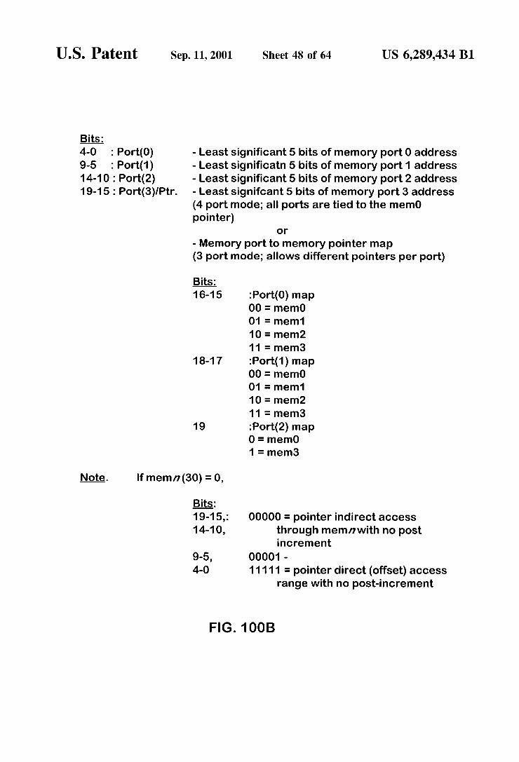
BitS: 4-0 : Port(O) - Least significant 5 bits of memory port 0 address 9-5 : Port(1) - Least significatin 5 bits of memory port 1 address 14-10: Port(2) - Least significant 5 bits of memory port 2 address 19-15: Port(3)/Ptr. - Least signifcant 5 bits of memory port 3 address
(4 port mode; all ports are tied to the mem0 pointer)
Or
- Memory port to memory pointer map (3 port mode; allows different pointers per port)
Bits: 16-15 :Port(O) map
00F memo 01 F mem.1 10 E mem2 11 F mem3
18-17 : Port(1) map OOE mem) 01 = mem1 10 E mem2 11 E mem3
19 : Port(2) map OF memO 1 F mem3
Note. lf memn (30) = 0,
Bits: 19-15,: 00000 = pointer indirect access 14-10, through memn with no post
increment 9-5, OOOO1 - 4-0 11111 = pointer direct (offset) access
range with no post-increment
FIG. 1 OOB

U.S. Patent Sep. 11, 2001
if memn (30) = 1,
Sheet 49 of 64 US 6,289,434 B1
BitS: 19-15,: 00000 = pointer indirect access 14-10, through memn with no post
increment 9-5, OOOO1 - 4-0 11011 = pointer direct (offset)
access range with no post increment
11100 = post increment memn by into 11101 = post increment memn by in1 11110 = post increment memn by int2 11111 = post increment memn by in3
22-20: Opr. - 3 bit Routing dictionary address (8 locations). Defined as follows.
In two and three operation mode: 22-20: Opr - 3 bit routing dictionary address.
In one operation mode: 22-20: Or. - I - Operand definitions.
000 = ports 0,1 and 2 are defined by pointer map in field 3
001 = ports 0 and 2 are defined by pointer map in field 3 and portfield 1 is a 5 bit unsigned immediate value.
010 F reserved
011 = portfields 0 and 1 form a 10 bit unsigned immediate value input, port 2 is the second input and port 3 is the output (all ports are mem0).
A/G 70OO

U.S. Patent Sep. 11, 2001 Sheet 50 of 64 US 6,289,434 B1
11 x = port 3 is a memo input and bits 14 to 0 represent the least significant 15 bits of 16 bit signed immediate data while bit 20 is the most significant bit (16th bit), where the output goes to the execution unit's register, ie, alu, bmu or mau.
28-23: - Operation dictionary addresses. Defined as follows.
In three operation mode: 24-23: BS - 2 bit BMU dictionary address (lower 4 locations) 26-25: A - 2 bit ALU dictionary address (lower 4 locations) 28-27: Ma - 2 bit MAU dictionary address (lower 4 locations)
In two operation mode: 25-23: AB - 3 bit ALU or BMU dictionary address (all 8
locations) 28-26: MA - 3 bit MAU or ALU dictionary address (all 8
locations)
In one operations mode: 28-23: MAB - Defines extended MAU, ALU and BMU dictionary
aCCSS
28-27: Unit - Execution unit 00F reserved 01 FALU 1 O BMU 11 E MAU
26-23: Addr. -Dictionary address of execution unit (16 locations)
A/G 700A

U.S. Patent Sep. 11, 2001 Sheet 51 of 64 US 6,289,434 B1
31-29:GO - Group Opcode. 000 = Non-computational Instruction 001 = 2 operation mode, ALU and BMU (4 ports) 010 = 2 operation mode, ALU and MAU (4 ports) 011 = 3 operation mode, MAU, BMU and ALU (4 ports) 100 = 1 operation mode 101 = 2 operation mode, ALU and BMU (3 mapped
ports) 110 = 2 operation mode, ALU and MAU (3 mapped
ports) 111 = 3 operation mode, MAU, BMU and ALU (3
mapped ports)
A/G 100AF
A/G 1004 A/G 7OOA A/G 100C A/G 1000 A/G 100AF
A/G 700

U.S. Patent Sep. 11, 2001 Sheet 52 of 64 US 6,289,434 B1
31 16 15 8 7 6 5 10 Reserved
BitS: o C - Conditional (use condition code) or Unconditional
Operation O = Unconditional 1 = Conditional
N.B. During a SIMD conditional execution instruction, if the result is to be written to memory, than a write is performed only if all the conditions are true. Eg. In 16 bit SIMD precision both words have to have true conditions for a write to be peformed. On the other hand, the output register is updated on a byte, word or dword basis.
5-1 : CCode - 5 bit Condition Code (check condition code table)
N.B. in 32bit mode, all four byte flags are set the same as the most significant byte. In the 16 bit SIMD mode, flags for bytes 3 and 2 are set the same as that for byte 3 and flags for byte 1 and 0 are set the same as the flag for byte 1.
7-6 : Pre. - Precision of the operation 00 = 32 bit precision 01 = 16 bit SIMD precision 10 = 08 bit SIMD precision 11 E Reserved
15-8: Opcode - Operation Opcode (defined below) Note. All opcodes are based on input operands to the MAU of A and B with an output Z. Eg.
Z = A <opmau> B
FIG. 101A

U.S. Patent
BitS:
Sep. 11, 2001 Sheet 53 of 64 US 6,289,434 B1
15 : Basic/Extended instructions
BitS: 8
10
OF Basic instructions
: input A data format 0 = unsigned 1 F signed : input B data format 0 F unsigned 1 = signed : carry (from previous operation) O = do not include carry 1 F include carry
13 : Multiply switch O = No multiply
BitS: 12-11 : Absolute value
11 Fabsolute Value
00,01,10 = negate input switch
Bits: 11 : input A sign operation
O EA 1 F -A
12 : input B sign operation O EB E-B
1 = multiply
A/G 107A

U.S. Patent Sep. 11, 2001 Sheet 54 of 64 US 6,289,434 B1
BitS: 12-11 : Multiply-Accumulation operation
00F multiply accummulator 01 F multiply - accummulator 10 = accummulator - multiply 11 = multiply only
14 : Output Saturation control O = No output saturation 1 = output saturated
1 F Extended instructions BitS: 10-8 : Reserved
A/G 107C A/G 1074 A/G 107A A/G 101C
A/G 707

U.S. Patent Sep. 11, 2001 Sheet 55 of 64 US 6,289,434 B1
31 16 15 8 7 6 5 10 Pre
Bits: O : C -Conditional (use condition code) or Unconditional
Operation OF Unconditional 1 F Conditional
5-1 : CCode - 5 bit Condition Code (check condition code table) 7-6 : Pre - Precision of the operation
00 = 32 bit precision 01 = 16 bit SIMD precision 10 = 08 bit SIMD precision 11 EReserved
15-8: Opcode - Operation Opcode (see following table) Note. All opcodes are based on input operands to the ALU of A and B with an output Z. Eg.
Z= A Copalud B Bits: 15 : Basic/Extended instructions
OF Basic instructions
Bits: 13 : Logical or Arithmetic Operations on ALU
1 F Logical
Bits: 8 : reserved 9 : OR type
O = OR 1 = XOR
10 : Logical operation O AND 1 = ORIXOR
F.G. 102A

U.S. Patent Sep. 11, 2001 Sheet 56 of 64 US 6,289,434 B1
11 : Complement bit for input A O EA 1E NOT.A
12 : Complement bit for input B O EB 1 E. NOT.B
OF Arithmetic
Bits: 8 : input A data format
0 F unsigned 1F signed
9 : input B data format 0 = unsigned F signed
10 : Carry (from previous operation) 0 = do not include carry 1 F include carry
12-11: NegatelAbsolute value 11 = absolute value of result at output 00,01,10 F negate bits for inputs A and B BitS: 11 : input. A sign operation
O FA 1 F -A
12 : input B sign operation O EB 1 E-B
14 : Output Saturation control O = No output saturation 1 = output saturated A/G. 702A
1 F Extended instructions Bits: A/G 7024 IS A/G 702A
A/G 702

U.S. Patent Sep. 11, 2001 Sheet 57 of 64 US 6,289,434 B1
31 16 15 8 7 6 5 10 Pre
BitS: O : C -Conditional (use condition code) or Unconditional
Operation OF Unconditional 1 = Conditional
5-1 : CCode - 5 bit Condition Code (check condition code table) 7-6 : Pre. - Precision of the operation
00 = 32 bit precision 01 = 16 bit SIMD precision 10 = 08 bit SIMD precision 11 F Reserved
15-8 : Opcode - Operation Opcode (see following table)
Bits:
Note. All opcodes are based on input operands to the BMU of A and B with an output Z. Eg.
ZF A Copbmud B
8 : Left/Right for shifts and rotates O = Left 1 = Right
9 : Shift/Rotate O = Shift 1 F Rotate
10 : Arithmetic/Logical 0 = Logical 1 = Arithmetic (sign extension)
12-11: Input Data Type 00F 32 bit data 01 F 16 bit data 10 = 08 bit data 11 F Reserved
13 : Insert Switch O = Off
1 E On A/G 70.3

U.S. Patent Sep. 11, 2001 Sheet 58 of 64 US 6,289,434 B1
31 29 28 24 23 21 20 16 15 13 12 8 7 5 4 O Width Shift Width shift Width shift Width shift SIMDBVte 3 SIMDBVte 2 SIMDBVte 1 SIMDBVte O
A76, 704
31 24, 23 20 19 16 15 8 7 4 3 O Reserved width shift Reserved width shift
SIMD word 1 SIMD word O 14 : Output Saturation control
O = No output saturation 1 = output saturated
15 : Extended instructions
A/G 706
3 3.22222222221111111111987654.3210 1 O9876543.210987654.3210 | | | | | | | | | 10ES MAU BMU ALU 10ES MAU BMU ALU
entr address entr S.
15-0 : Defines an even address routing dictionary entry.
2-0, : ALU -Input/output port and register route encoding for each unit
6-4, : BMU Encoding A 10-8 : MAU 000 = Inputs: port (O),port (1) output: port'(3)/reg?
001 = Inputs: port (O),alu Output: port'(3)/reg 010 = Inputs: port (0),bmu Output: port'(3)l reg 011 = Inputs: port (0), mau Output: port'(3)/reg 1005= inputs: port (0), port (3) Output: port(2)/regy 101 = Inputs: bmu,alu Output: port'(3)/reg 110 = Inputs: mau,bmu Output: port'(3)/reg 111 = Inputs: alu,mau Output: port'(3)/reg
A/G 70.64

U.S. Patent Sep. 11, 2001 Sheet 59 of 64 US 6,289.434 B1
Encoding B1 000 = Inputs: port (0), port (1) Output: port (2)/regy 001 F inputs: bmu,port (1) Output: port (2)/reg 010 = Inputs: mau, port (1) Output: port (2)/reg 011 = Inputs: alu, port (1) Output: port (2)/reg 100 = Inputs: port (2), port (1) Output: port(3)" reg 101 = Inputs: bnu,alu Output: port (2)/reg 110F Inputs: mau,bmu Output: port (2)/reg 111 = Inputs: alu, mau Output: port (2)/regy
Encoding C1 000 = Inputs: port (0), port (1) Output: port'(3)/reg 001 = Inputs: port (2),alu Output: port(3)/reg 010 = Inputs: port (2),bmu Output: port(3)/reg 011 = Inputs: port (2),mau Output: port(3)/reg 1005= Inputs: port (2),port (3) Output: reg 101 = Inputs: brmu, alu Output: port'(3)/reg 110 = Inputs: mau,bmu Output: port'(3)/reg 111 = Inputs: alu, mau Output: port'(3)/reg
3, : AS - Output selectors for the various execution units 7, : Bs 1 = Output is to the respective execution unit's output
register 11 : Ms 0 = Output is to a port
13-12: Es - Encoding Selector LSBs for ALU-BMU-MAU Two Operation Mode (ALU-BMU)
x0 = ALU - Encoding A, BMU - Encoding B x1 = ALU - Encoding B, BMU - Encoding A
TWO Operation Mode (ALU-MAU) x0= ALU - Encoding A, MAU- Encoding B x1 = ALU - Encoding B, MAU- Encoding A
Three Operation Mode (ALU-BMU-MAU) 00 = ALU - Encoding A, BMU- Encoding B,
MAU- Encoding C 01 = ALU - Encoding B, BMU - Encoding C,
MAU- Encoding A 10 = ALU - Encoding C, BMU - Encoding B,
A/G 70.6A MAU- Encoding A 11 = ALU - Encoding B, BMU- Encoding A,
MAU- Encoding B
U.S. Patent Sep. 11, 2001 Sheet 60 of 64 US 6,289,434 B1
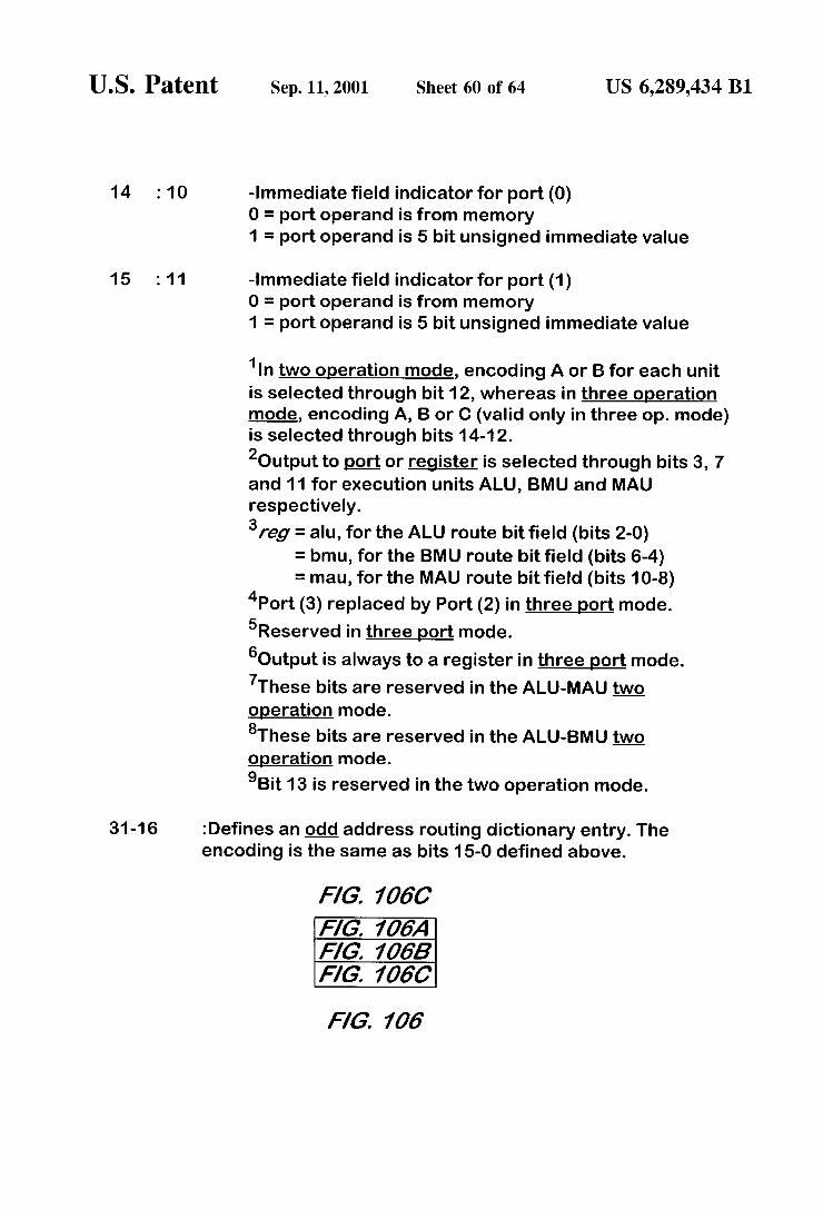
14 : 10 -Immediate field indicator for port (O) 0 = port operand is from memory 1 F port operand is 5 bit unsigned immediate value
15 : 11 -Immediate field indicator for port (1) OF port operand is from memory 1F port operand is 5 bit unsigned immediate value
in two operation mode, encoding A or B for each unit is selected through bit 12, whereas in three operation mode, encoding A, B or C (valid only in three op. mode) is selected through bits 14-12. output to port or register is selected through bits 3, 7 and 11 for execution units ALU, BMU and MAU respectively. reg = alu, for the ALU route bitfield (bits 2-0)
=bmu, for the BMU route bitfield (bits 6-4) = mau, for the MAU route bitfield (bits 10-8)
Port (3) replaced by Port (2) in three port mode. Reserved in three port mode. Output is always to a register in three port mode. These bits are reserved in the ALU-MAU tWO operation mode. These bits are reserved in the ALU-BMU two Operation mode. Bit 13 is reserved in the two operation mode.
31-16 : Defines an odd address routing dictionary entry. The encoding is the same as bits 15-0 defined above.
A/G 106C A/G 7064 A/G 106A A/G 7O6O.
A/G 706

U.S. Patent Sep. 11, 2001 Sheet 61 of 64 US 6,289,434 B1
31 25 0. 26 Bit Source BVte Address
A/G 707
31 25 O 26 Bit Destination Bvte Address
A/G 103
31 24 23 16 15 12 11 O Height (bytes) Res. Width (bytes
A/G 70.9
31 24, 23 1615 12 11 O Reserved Destination Warp (bvtes Res. Source Warp (bvtes
A/G 770
31 8 7 4 3 O Reserved ID | Comm. Byte En.
BitS: 3-0 : Byte Enables 4. : Horizontal address increment direction
O = Left to Right 1 = Right to Left
5 :Vertical address increment direction O = Left to Right 1 = Right to Left
6 : External address space OF Source is External 1 F Destination is External
A/G 7774

U.S. Patent Sep. 11, 2001 Sheet 62 of 64 US 6,289,434 B1
7 : DMA address space O = Source and destination are within UMP space 1 = Either source or destination is outside UMP space
8 : DMA transfer complete (this bit is set by hardware) O = Transfer complete 1 = Transfer in progress
A/G 777A A/G 7774 A/G 777A
A/G 777
0x04 TDMA Command Register (DMAC Source and Destination 2-D Warp Factor Register (WARP)
0x02 Transfer Size Register (TSR) OXO1 Destination ByteAddress Register (DAR) 0x00 Source ByteAddress Register (SAR)
A/G 77.2
a; ; ; ; ; aggaggles? 1 O 9 8 7 6 5 4 3 2 1 O9876543.210 Reserved TTTT TTTTTTTTTTTTTT E"::::::::::B; LLILL SS II CCCCEEEE
Bits: 3-0 : TxE - Timer O/1/2/3 Enable BitS
OF Start timer 1 = Stop timer
7-4 : TXC - Timer Ol11213 Continuous loop Bits O = Single loop 1 = Continuous loop
A/G 7734

U.S. Patent Sep. 11, 2001 Sheet 63 of 64 US 6,289,434 B1
11-8 : Tx - Timer Ol1/2/3 Generate Interrupt Bits O = No interrupt Generated 1 = Generate Interrupt
12 : TOS -Timer O Scale? Timer Switch O = Independent timer 1 F Scaling counter for Timer 1 (32bit mode)
13 : T2S - Timer 2 Scale/Timer Switch 0 = independent timer 1 = Scaling counter for Timer 3 (32bit mode)
15-14 : Reserved 19-16 : Tx. -Timer O/1/2/3 Lock BitS
0 = Timer Unlocked (timer not in use) 1 = Timer Locked (timer in use)
31-20 : Reserved
A/G 773A
A/G 773
U.S. Patent Sep. 11, 2001 Sheet 64 of 64 US 6,289,434 B1
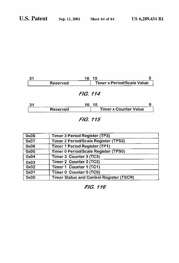
31 16 15 O Timer X Period/Scale Value
A/G 774
31 16 15 O Timer X Counter Value
A/G 776
Timer 3 Period Register (TP3)
0x06 Timer 1 Period Register (TP1) 0x05 Timer O Period/Scale Register (TPSO) 0x04 Timer 3 Counter 3 (TC3) 0x03 Timer 2 Counter 2 (TC2) 0x02 Timer 1 Counter 1 (TC1)
0x00 Timer Status and Control Register (TSCR) A/G 776
US 6,289,434 B1 1
APPARATUS AND METHOD OF IMPLEMENTING SYSTEMS ON SLICON USING DYNAMIC-ADAPTIVE RUN-TIME RECONFIGURABLE CIRCUITS FOR
PROCESSING MULTIPLE, INDEPENDENT DATA AND CONTROL STREAMS OF
WARYING RATES
RELATED APPLICATION
This application claims the benefit of U.S. Provisional Application No. 60/039,237 entitled, “APPARATUS AND METHOD OF IMPLEMENTING SYSTEMS ON SIL CON USING DYNAMIC-ADAPTIVE RUN-TIME RECONFIGURABLE CIRCUITS FOR PROCESSING MULTIPLE, INDEPENDENT DATA AND CONTROL STREAMS OF VARYING RATES” filed on Feb. 28, 1997 by Rupan Roy and is hereby incorporated herein by refer ence in its entirety.
COPYRIGHT AUTHORIZATION
A portion of the disclosure of this patent document contains material which is Subject to copyright protection. The copyright owner has no objection to the facsimile reproduction by anyone of the patent document or the patent disclosure, as it appears in the Patent and Trademark Office patent file or records, but otherwise reserves all copyright rights whatsoever.
FIELD OF THE INVENTION
The present invention pertains to the field of runtime reconfigurable dynamic-adaptive digital circuits which can implement a myriad of digital processing functions related to Systems control, digital Signal processing, communications, image processing, Speech and Voice rec ognition or Synthesis, three-dimensional graphics rendering, Video processing. High definition television, cellular and broadcast radio, neural networks, etc.
BACKGROUND OF THE INVENTION
To date, the most common method of implementing various functions on an integrated circuit is by Specifically designing the function or functions to be performed by placing on Silicon an interconnected group of digital circuits in a non-modifiable manner (hard-wired or fixed function implementation.) These circuits are designed to provide the fastest possible operation of the circuit in the least amount of Silicon area. In general these circuits are made up of an interconnection of various amounts of random-access memory and logic circuits. Complex Systems on Silicon are broken up into Separate blockS and each block is designed Separately to only perform the function that it was intended to do. In Such Systems, each block has to be individually tested and validated, and then the whole System has to be tested to make Sure that the constituent parts work together. This proceSS is becoming increasingly complex as we move into future generations of Single-chip System implementa tions. Systems implemented in this way generally tend to be the highest performing Systems Since each block in the System has been individually tuned to provide the expected level of performance. This method of implementation may be the Smallest (cheapest in terms of Silicon area) method when compared to three other distinct ways of implementing such systems today. Each of these other three have their problems and generally do not tend to be the most cost effective solution. These other methods are explained below.
15
25
35
40
45
50
55
60
65
2 Any System can be functionally implemented in Software
using a microprocessor and associated computing System. Such systems would however, not be able to deliver real time performance in a cost-effective manner for the class of applications that was described above. Today Such Systems are used to model the Subsequent hard-wired/fixed-function System before considerable design effort is put into the System design. The Second method of implementing Such Systems is by
using a digital Signal processor or DSP. This class of computing machines is useful for real-time processing of certain speech, audio, video and image processing problems. They may also be effective in certain control functions but are not cost-effective when it comes to performing certain real time tasks which do not have a high degree of paral lelism in them or tasks that require multiple parallel threads of operation Such as three-dimensional graphics. The third method of implementing such systems is by
using field programmable gate arrays or FPGAS. These devices are made up of a two-dimensional array of fine grained logic and Storage elements which can be connected together in the field by downloading a configuration Stream which essentially routes Signals between these elements. This routing of the data is performed by pass-transistor logic. FPGAs are by far the most flexible of the three methods mentioned. The problem with trying to implement complex real-time systems with FPGAs is that although there is a greater flexibility for optimizing the Silicon usage in Such devices, the designer has to trade it off for increase in cost and decrease in performance. The performance may (in Some cases) be increased considerably at a significant cost, but still would not match the performance of hard wired fixed function devices.
It can be seen that the above mentioned Systems do not reduce the cost or increase the performance over fixed function Silicon Systems. In fact, as far as performance is concerned fixed-function Systems Still out perform the above mentioned Systems for the same cost. The three Systems mentioned can theoretically reduce cost
by removing redundancy from the System. Redundancy is removed by re-using computational blocks and memory. The only problem is that these Systems themselves are increas ingly complex, and therefore, their computational density when compared with fixed-function devices is very high. Most systems on silicon are built up of complex blocks of
functions that have varying data bandwidth and computa tional requirements. AS data and control information moves through the System, the processing bandwidth varies enor mously. Regardless of the fact that the bandwidth varies, fixed-function Systems have logic blocks that exhibit a “temporal redundancy' that can be exploited to drastically reduce the cost of the System. This is true, because in fixed function implementations all possible functional require ments of the necessary data processing has to be imple mented on the Silicon regardless of the final application of the device or the nature of the data to be processed. Therefore, if a fixed function device has to adaptively process data, then it has to commit Silicon resources to process all possible flavors of the data. Furthermore, State variable Storage in all fixed function Systems are imple mented using area inefficient Storage elements Such as latches and flip-flops.
It is the object of the present invention to provide a new method and apparatus for implementing Systems on Silicon or other material which will enable the user a means for achieving the performance of fixed-function implementa
US 6,289,434 B1 3
tions at a lower cost. The lower cost is achieved by removing redundancy from the System. The redundancy is removed by re-using groups of computational and Storage elements in different configurations. The cost is further reduced by employing only Static or dynamic ram as a means for holding the State of the System. This invention provides a means of effectively adapting the configuration of the circuit to varying input data and processing requirements. All of this reconfiguration can take place dynamically in run-time without any degradation of performance over fixed function implementations.
SUMMARY OF THE INVENTION
According to the present invention, apparatus and method are provided for adaptively dynamically reconfiguring groups of computational and Storage elements in run-time to proceSS multiple Separate Streams of data and control at varying rates. The aggregate of the dynamically reconfig urable computational and Storage elements will heretofore be referred to as a “media processing unit'. In one embodi ment a plurality of Said media processing units are inter connected in a matrix using a reconfigurable memory mapped pipelined communication/data transfer protocol.
BRIEF DESCRIPTION OF THE INVENTION
FIG. 1 depicts an integrated circuit comprising a plurality of media processing units. Furthermore, a plurality of Such integrated circuits could be connected together to form a larger System.
All communication and transfer of data within any Such System is based on a memory map. Every Single State variable in Such a System occupies a place on a System memory map. All reconfiguration between multiple media processing units be they on or off chip, is through the memory map. Routing of data and control information proceeds through the System by associating an address with the information.
The media processing units comprise multiple blocks of memory which act as the State variable Storage elements (which can be dynamic ram or static ram) and multiple blocks of various computational units. FIG. 2 depicts the memory blocks and the computational units connected together by a reconfigurable routing matrix. The reconfig urable routing matrix can dynamically, on a per clock basis, be Switched to present a different configuration.
The dynamic routing of the computational units is folded into the pipeline of the machine So that routing delays do not inhibit the speed of operation of the device. The depth of the pipeline can be varied depending on the complexity and performance required out of the device. In cases of deeper pipelines, multi-threaded applications can be run through the Same media processing unit to alleviate problems with pipeline latencies.
The configuration data for the computational blocks con sist of information that determines the operation that a Specific block will perform, its data dependencies on the results from other blocks and the precision of its input and output data. The precision of the input data may be different from the precision of its output data.
The configuration data for the routing consists of infor mation regarding the routing of data between various com putational blocks themselves and also between computa tional blocks and the Storage elements (memory).
All configuration data is placed in normal memory much like data and is accessed on a pipeline basis much the same way as data, i.e., configuration data is treated just like any other data.
15
25
35
40
45
50
55
60
65
4 Within the media processing units there is a hierarchy of
routing referred to as “micro-routing” and "macro-routing”. Micro-routing refers to routing within macro data types Such as 32, 16 or 8 bit data. In micro-routing signals (bits) can be individually routed between various macro data types to emulate fixed-function (hard-wired) designs. Macro-routing routes macro-data width connections between computa tional elements and computational elements and Storage elements.
The adaptive nature of the invention comes from the fact that the configuration information can be changed on the fly by the nature of the data that is being processed. The configuration information can be accessed and modified at any time and is treated just like any other data. A particular application is mapped onto the device by
Studying its computational complexity and performance requirements. The application is broken up into Separate blocks which perform the functions required. The inputs, outputs and bandwidth requirements of each of these Smaller blockS is determined. The various configurations of media processing units, computational and Storage elements is then determined from the specification of the smaller blocks. The cycle or Sequence of both computational unit con
figuration and routing configuration that is required to implement a Specific function is the instruction Sequence of that particular function and is herein referred to as the “Software” that drives the device.
In FIG. 3, an embodiment of the invention, eight (8) media processing units (MPUs) are interconnected through a pipelined communication and data transfer wiring Scheme which essentially consists of four (4) bi-directional 64 bit buSSes. Data transfer to and from media processing units is managed through memory mapped locations.
Each of these units is capable of executing one or a multiple of complex 32 bit media instructions per clock cycle. This instruction Stream forms the configuration Sequence for both the computational, Storage and routing elements of the units. This complex media instruction may configure the media processing unit to execute three con current 32 bit arithmetic or logical operations in parallel while accessing four 32 bit data words from memory and also performing four memory address computations, all this in a Single clock cycle. All the computational units have a 32 bit data path in the current embodiment except for the multiplier-accumulator unit which has a 64-bit accumulator. These data paths can be split into multiple 8 or 16 bit data paths working in a SIMD mode of operation. Each complex media instruction is comparable to multiple simple DSP like instructions.
The present embodiment of the invention has two (2) computational units within each media processing unit. These two units are a 32 bit Multiplier whose output can be accumulated to 64bits (MAU) and a 32 bit Arithmetic Logic Unit (ALU). A 32 bit micro-router (BMU) with 64 bit input and 32 bit output is also present. The two computational units and the micro-router can be configured to implement pipelined 32 bit Single Precision IEEE Floating Point Multiplies, Adds and Divides. This greatly enhances the capability of the device to implement complex modem, audio and 3-D applications.
Since each of the MPUs are virtually identical to each other, writing Software (the configuration sequence) becomes very easy. The RISC-like nature of each of these media processing units also allows for a consistent hardware platform for simple OS and driver development. Any one of the MPU's can take on a Supervisory role and act as a central
US 6,289,434 B1 S
controller if necessary. This can be very useful in Set-top box applications where a Controlling CPU will not be neceSSary.
All communication on chip is memory based, i.e., all the processing units (MPUs, Video interface, etc) lie on a 64MB memory map and communication between these units and the units and local memory is through simple memory reads and writes. Here a processing unit refers to the MPUs as well as all the peripheral controllers. These peripheral con trollers consist of the PCI interface, Video capture interface, Audio Codec and Telecommunications interface and the Video Display interfaces. Therefore, besides there being DMA pathways for all these peripheral interfaces, there also exists “through processor pathways for all input and output media data. This allows for pre and post-processing of all data types going into and coming out of memory, thereby greatly reducing memory bandwidth. This processing can be done “on the fly” because of the very high speed at which each of the MPU's operate.
Operation of the MPU's can be interrupted by the various peripheral interface units. This allows for “object oriented” media types to be implemented. Memory fill/empty level trigger points can be set up for the various peripheral interfaces which interrupt particular MPU's that can then service these interrupts “on the fly'.
BRIEF DESCRIPTION OF THE DRAWINGS
FIG. 1 is a block Schematic diagram of an integrated circuit containing a plurality of media processing units according to one embodiment of the present invention.
FIG. 2 is a block schematic diagram of memory blocks and computational units of the integrated circuit of FIG. 1.
FIG.3 is a block Schematic diagram of a System according to one embodiment of the present invention.
FIG. 4, a concatenation of FIGS. 4A and 4B is a memory map illustrating the arrangement of a memory Space accord ing to one embodiment of the present invention.
FIG. 4C is a memory map illustrating the arrangement of an MPU address/transfer word according to one embodi ment of the present invention.
FIG. 5 is a timing diagram illustrating timing of a non burst read according to one embodiment of the present invention.
FIG. 6 is a timing diagram illustrating timing of a burst read according to one embodiment of the present invention.
FIG. 7 is a timing diagram illustrating timing of a non burst write according to one embodiment of the present invention.
FIG. 8 is a timing diagram illustrating timing of a burst write according to one embodiment of the present invention.
FIG. 9 is a memory map illustrating the effect of a first example shift left bit manipulation performed with 32 bit precision on a Dword data type input by a bit manipulation unit according to one embodiment of the present invention.
FIG. 10 is a memory map illustrating the effect of a Second example logical shift left bit manipulation performed with 32 bit precision on a Dword data type input by a bit manipulation unit according to one embodiment of the present invention.
FIG. 11 is a memory map illustrating the effect of a third example logical shift left bit manipulation performed with 32 bit precision on a Dword data type input by a bit manipulation unit according to one embodiment of the present invention.
1O
15
25
35
40
45
50
55
60
65
6 FIG. 12 is a memory map illustrating the effect of a first
example logical shift left bit manipulation performed with 32 bit precision on a Word data type input by a bit manipu lation unit according to one embodiment of the present invention.
FIG. 13 is a memory map illustrating the effect of a Second example logical shift left bit manipulation performed with 32 bit precision on a Word data type input by a bit manipulation unit according to one embodiment of the present invention.
FIG. 14 is a memory map illustrating the effect of a third example logical shift left bit manipulation performed on a Word data type input by a bit manipulation unit according to one embodiment of the present invention.
FIG. 15 is a memory map illustrating the effect of a first example logical shift left bit manipulation performed with 32 bit precision on a Byte data type input by a bit manipu lation unit according to one embodiment of the present invention.
FIG. 16 is a memory map illustrating the effect of a Second example logical shift left bit manipulation performed with 32 bit precision on a Byte data type input by a bit manipulation unit according to one embodiment of the present invention.
FIG. 17 is a memory map illustrating the effect of a third example logical shift left bit manipulation performed with 32 bit precision on a Byte data type input by a bit manipu lation unit according to one embodiment of the present invention.
FIG. 18 is a memory map illustrating the effect of a first example logical shift left bit manipulation performed with 16 bit precision SIMD on a Word data type input by a bit manipulation unit according to one embodiment of the present invention.
FIG. 19 is a memory map illustrating the effect of a Second example logical shift left bit manipulation performed with 16 bit precision SIMD on a Word data type input by a bit manipulation unit according to one embodiment of the present invention.
FIG. 20 is a memory map illustrating the effect of a third example logical shift left bit manipulation performed with 16 bit precision SIMD on a Word data type input by a bit manipulation unit according to one embodiment of the present invention.
FIG. 21 is a memory map illustrating the effect of a first example logical shift left bit manipulation performed with 16 bit precision SIMD on a Byte data type input by a bit manipulation unit according to one embodiment of the present invention.
FIG. 22 is a memory map illustrating the effect of a Second example logical shift left bit manipulation performed with 16 bit precision SIMD on a Byte data type input by a bit manipulation unit according to one embodiment of the present invention.
FIG. 23 is a memory map illustrating the effect of a first example logical shift left bit manipulation performed with 8 bit precision STMD on a Byte data type input by a bit manipulation unit according to one embodiment of the present invention.
FIG. 24 is a memory map illustrating the effect of a Second example logical shift left bit manipulation performed with 8 bit precision SIMD on a Byte data type input by a bit manipulation unit according to one embodiment of the present invention. FIG.25 is a memory map illustrating the effect of a third
example logical shift left bit manipulation performed with 8

US 6,289,434 B1 7
bit precision SIMD on a Byte data type input by a bit manipulation unit according to one embodiment of the present invention.
FIG. 26 is a memory map illustrating the effect of a first example logical shift left bit manipulation performed with 8 bit precision SIMD on a Word data type input by a bit manipulation unit according to one embodiment of the present invention.
FIG. 27 is a memory map illustrating the effect of a Second example logical shift left bit manipulation performed with 8 bit precision SIMD on a Word data type input by a bit manipulation unit according to one embodiment of the present invention.
FIG. 28 is a memory map illustrating the effect of a first example arithmetic shift left bit manipulation performed with 32 bit precision on a Dword data type input by a bit manipulation unit according to one embodiment of the present invention.
FIG. 29 is a memory map illustrating the effect of a Second example arithmetic shift left bit manipulation per formed with 32 bit precision on a Dword data type input by a bit manipulation unit according to one embodiment of the present invention.
FIG. 30 is a memory map illustrating the effect of a third example arithmetic shift left bit manipulation performed with 32 bit precision on a Dword data type input by a bit manipulation unit according to one embodiment of the present invention.
FIG. 31 is a memory map illustrating the effect of a first example arithmetic shift left bit manipulation performed with 32 bit precision on a Word data type input by a bit manipulation unit according to one embodiment of the present invention.
FIG. 32 is a memory map illustrating the effect of a Second example arithmetic shift left bit manipulation per formed with 32 bit precision on a Word data type input by a bit manipulation unit according to one embodiment of the present invention.
FIG. 33 is a memory map illustrating the effect of a third example arithmetic shift left bit manipulation performed with 32 bit precision on a Word data type input by a bit manipulation unit according to one embodiment of the present invention.
FIG. 34 is a memory map illustrating the effect of a first example arithmetic shift left bit manipulation performed with 32 bit precision on a Byte data type input by a bit manipulation unit according to one embodiment of the present invention.
FIG. 35 is a memory map illustrating the effect of a Second example arithmetic shift left bit manipulation per formed with 32 bit precision on a Byte data type input by a bit manipulation unit according to one embodiment of the present invention.
FIG. 36 is a memory map illustrating the effect of a third example arithmetic shift left bit manipulation performed with 32 bit precision on a Byte data type input by a bit manipulation unit according to one embodiment of the present invention.
FIG. 37 is a memory map illustrating the effect of a first example arithmetic shift left bit manipulation performed with 16 bit precision SIMD on a Word data type input by a bit manipulation unit according to one embodiment of the present invention.
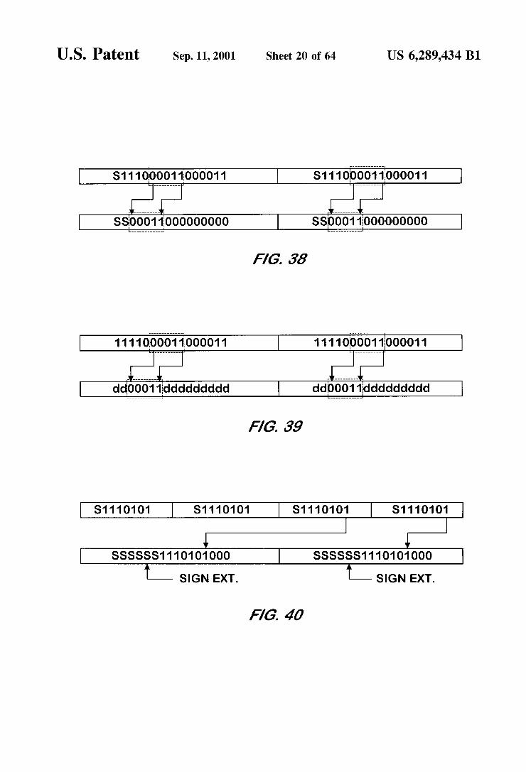
FIG. 38 is a memory map illustrating the effect of a Second example arithmetic shift left bit manipulation per
15
25
35
40
45
50
55
60
65
8 formed with 16 bit precision SIMD on a Word data type input by a bit manipulation unit according to one embodi ment of the present invention.
FIG. 39 is a memory map illustrating the effect of a third example arithmetic shift left bit manipulation performed with 16 bit precision SIMD on a Word data type input by a bit manipulation unit according to one embodiment of the present invention.
FIG. 40 is a memory map illustrating the effect of a first example arithmetic shift left bit manipulation performed with 16 bit precision SIMD on a Byte data type input by a bit manipulation unit according to one embodiment of the present invention.
FIG. 41 is a memory map illustrating the effect of a Second example arithmetic shift left bit manipulation per formed with 16 bit precision SIMD on a Byte data type input by a bit manipulation unit according to one embodiment of the present invention.
FIG. 42 is a memory map illustrating the effect of a first example arithmetic shift left bit manipulation performed with 8 bit precision SIMD on a Byte data type input by a bit manipulation unit according to one embodiment of the present invention.
FIG. 43 is a memory map illustrating the effect of a Second example arithmetic shift left bit manipulation per formed with 8 bit precision SIMD on a Byte data type input by a bit manipulation unit according to one embodiment of the present invention.
FIG. 44 is a memory map illustrating the effect of a third example arithmetic shift left bit manipulation performed with 8 bit precision SIMD on a Byte data type input by a bit manipulation unit according to one embodiment of the present invention.
FIG. 45 is a memory map illustrating the effect of a first example logical shift right bit manipulation performed with 32 bit precision on a Dword data type input by a bit manipulation unit according to one embodiment of the present invention.
FIG. 46 is a memory map illustrating the effect of a Second example logical shift right bit manipulation per formed with 32 bit precision on a Dword data type input by a bit manipulation unit according to one embodiment of the present invention.
FIG. 47 is a memory map illustrating the effect of a third example logical shift right bit manipulation performed with 32 bit precision on a Dword data type input by a bit manipulation unit according to one embodiment of the present invention.
FIG. 48 is a memory map illustrating the effect of a first example logical shift right bit manipulation performed with 32 bit precision on a Word data type input by a bit manipu lation unit according to one embodiment of the present invention.
FIG. 49 is a memory map illustrating the effect of a Second example logical shift right bit manipulation per formed with 32 bit precision on a Word data type input by a bit manipulation unit according to one embodiment of the present invention.
FIG. 50 is a memory map illustrating the effect of a third example logical shift right bit manipulation performed with 32 bit precision on a Word data type input by a bit manipu lation unit according to one embodiment of the present invention.
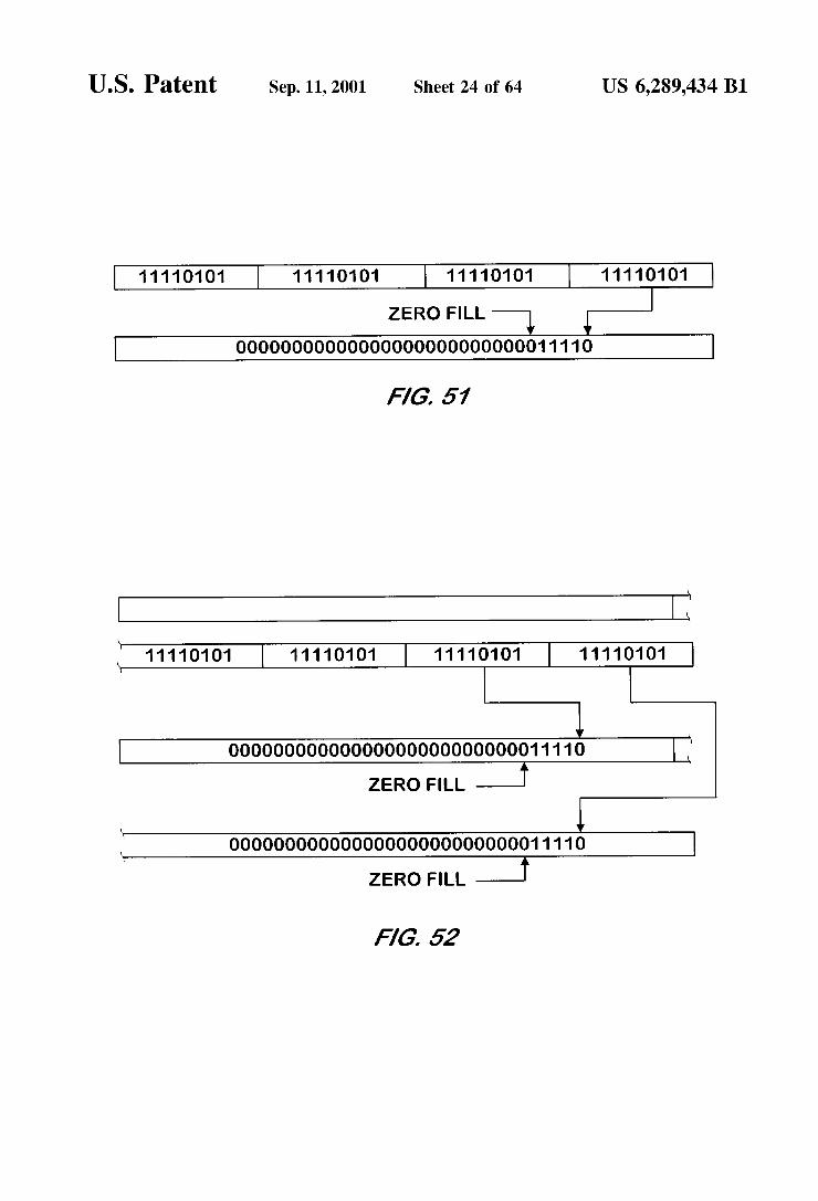
FIG. 51 is a memory map illustrating the effect of a first example logical shift right bit manipulation performed with

US 6,289,434 B1
32 bit precision on a Byte data type input by a bit manipu lation unit according to one embodiment of the present invention.
FIG. 52 is a memory map illustrating the effect of a Second example logical shift right bit manipulation per formed with 32 bit precision on a Byte data type input by a bit manipulation unit according to one embodiment of the present invention.
FIG. 53 is a memory map illustrating the effect of a third example logical shift right bit manipulation performed with 32 bit precision on a Byte data type input by a bit manipu lation unit according to one embodiment of the present invention.
FIG. 54 is a memory map illustrating the effect of a first example logical shift right bit manipulation performed with 16 bit precision SIMD on a Word data type input by a bit manipulation unit according to one embodiment of the present invention.
FIG. 55 is a memory map illustrating the effect of a Second example logical shift right bit manipulation per formed with 16 bit precision SIMD on a Word data type input by a bit manipulation unit according to one embodi ment of the present invention.
FIG. 56 is a memory map illustrating the effect of a third example logical shift right bit manipulation performed with 16 bit precision SIMD on a Word data type input by a bit manipulation unit according to one embodiment of the present invention.
FIG. 57 is a memory map illustrating the effect of a first example logical shift right bit manipulation performed with 16 bit precision SIMD on a Byte data type input by a bit manipulation unit according to one embodiment of the present invention.
FIG. 58 is a memory map illustrating the effect of a Second example logical shift right bit manipulation per formed with 16 bit precision SIMD on a Byte data type input by a bit manipulation unit according to one embodiment of the present invention.
FIG. 59 is a memory map illustrating the effect of a first example logical shift right bit manipulation performed with 8 bit precision SIMD on a Byte data type input by a bit manipulation unit according to one embodiment of the present invention.
FIG. 60 is a memory map illustrating the effect of a Second example logical shift right bit manipulation per formed with 8 bit precision SIMD on a Byte data type input by a bit manipulation unit according to one embodiment of the present invention.
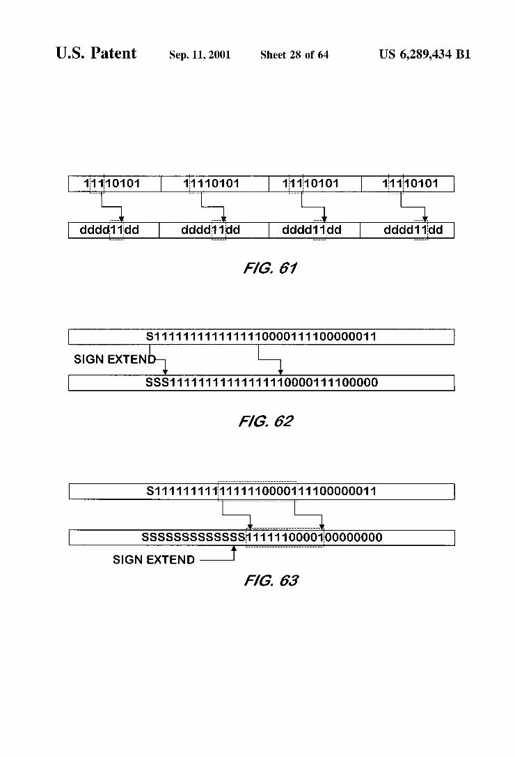
FIG. 61 is a memory map illustrating the effect of a third example logical shift right bit manipulation performed with 8 bit precision SIMD on a Byte data type input by a bit manipulation unit according to one embodiment of the present invention.
FIG. 62 is a memory map illustrating the effect of a first example arithmetic shift right bit manipulation performed with 32 bit precision on a Dword data type input by a bit manipulation unit according to one embodiment of the present invention.
FIG. 63 is a memory map illustrating the effect of a Second example arithmetic shift right bit manipulation per formed with 32 bit precision on a Dword data type input by a bit manipulation unit according to one embodiment of the present invention.
FIG. 64 is a memory map illustrating the effect of a third example arithmetic shift right bit manipulation performed
15
25
35
40
45
50
55
60
65
10 with 32 bit precision on a Dword data type input by a bit manipulation unit according to one embodiment of the present invention.
FIG. 65 is a memory map illustrating the effect of a first example arithmetic shift right bit manipulation performed with 32 bit precision on a Word data type input by a bit manipulation unit according to one embodiment of the present invention.
FIG. 66 is a memory map illustrating the effect of a Second example arithmetic shift right bit manipulation per formed with 32 bit precision on a Word data type input by a bit manipulation unit according to one embodiment of the present invention.
FIG. 67 is a memory map illustrating the effect of a third example arithmetic shift right bit manipulation performed with 32 bit precision on a Word data type input by a bit manipulation unit according to one embodiment of the present invention.
FIG. 68 is a memory map illustrating the effect of a fourth example arithmetic shift right bit manipulation performed with 32 bit precision on a Word data type input by a bit manipulation unit according to one embodiment of the present invention.
FIG. 69 is a memory map illustrating the effect of a fifth example arithmetic shift right bit manipulation performed with 32 bit precision on a Word data type input by a bit manipulation unit according to one embodiment of the present invention.
FIG. 70 is a memory map illustrating the effect of a first example arithmetic shift right bit manipulation performed with 32 bit precision on a Byte data type input by a bit manipulation unit according to one embodiment of the present invention.
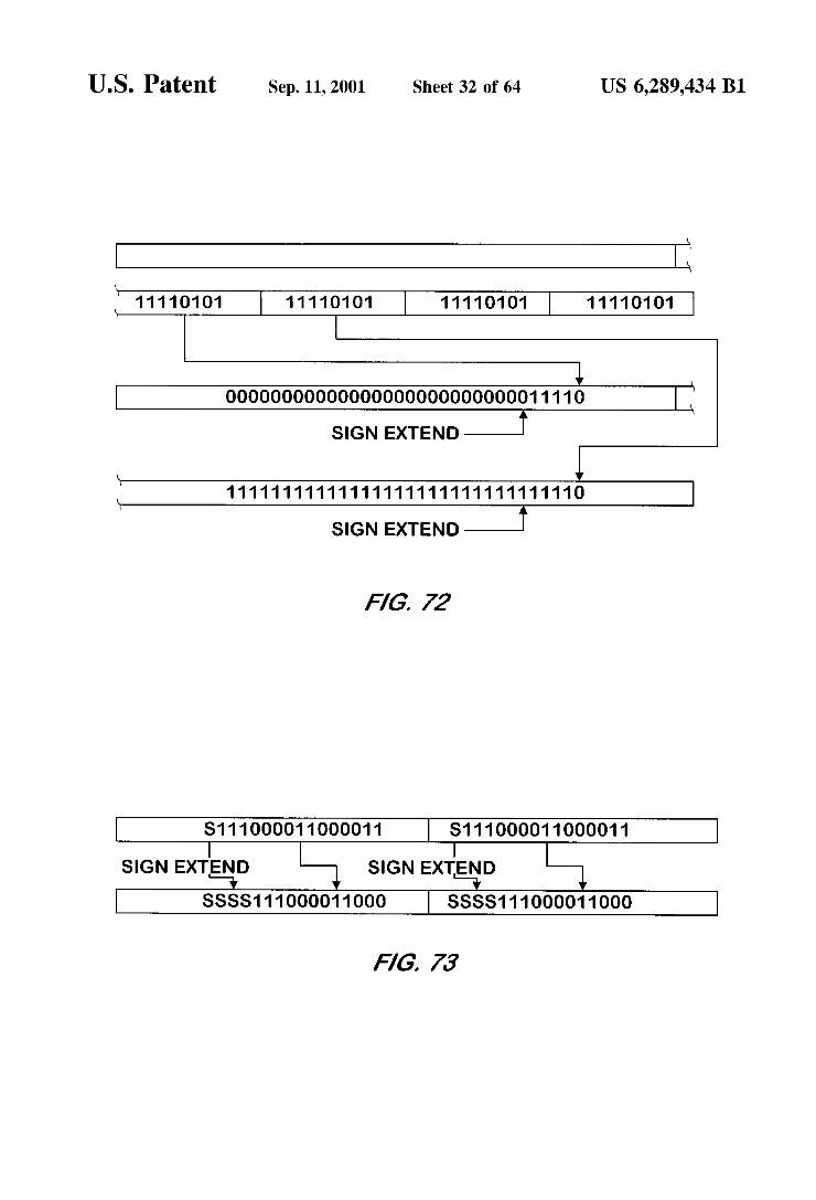
FIG. 71 is a memory map illustrating the effect of a Second example arithmetic shift right bit manipulation per formed with 32 bit precision on a Byte data type input by a bit manipulation unit according to one embodiment of the present invention. FIG.72 is a memory map illustrating the effect of a third
example arithmetic shift right bit manipulation performed with 32 bit precision on a Byte data type input by a bit manipulation unit according to one embodiment of the present invention.
FIG. 73 is a memory map illustrating the effect of a first example arithmetic shift right bit manipulation performed with 16 bit precision SIMD on a Word data type input by a bit manipulation unit according to one embodiment of the present invention.
FIG. 74 is a memory map illustrating the effect of a Second example arithmetic shift right bit manipulation per formed with 16 bit precision SIMD on a Word data type input by a bit manipulation unit according to one embodi ment of the present invention.
FIG. 75 is a memory map illustrating the effect of a third example arithmetic shift right bit manipulation performed with 16 bit precision SIMD on a Word data type input by a bit manipulation unit according to one embodiment of the present invention.
FIG. 76 is a memory map illustrating the effect of a first example arithmetic shift right bit manipulation performed with 16 bit precision SIMD on a Byte data type input by a bit manipulation unit according to one embodiment of the present invention.
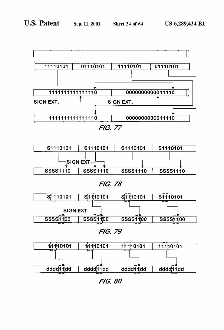
FIG. 77 is a memory map illustrating the effect of a Second example arithmetic shift right bit manipulation per

US 6,289,434 B1 11
formed with 16 bit precision SIMD on a Byte data type input by a bit manipulation unit according to one embodiment of the present invention.
FIG. 78 is a memory map illustrating the effect of a first example arithmetic shift right bit manipulation performed with 8 bit precision SIMD on a Byte data type input by a bit manipulation unit according to one embodiment of the present invention.
FIG. 79 is a memory map illustrating the effect of a Second example arithmetic shift right bit manipulation per formed with 8 bit precision SIMD on a Byte data type input by a bit manipulation unit according to one embodiment of the present invention.
FIG.80 is a memory map illustrating the effect of a third example arithmetic shift right bit manipulation performed with 8 bit precision SIMD on a Byte data type input by a bit manipulation unit according to one embodiment of the present invention.
FIG. 81 is a memory map illustrating the effect of an example arithmetic/logical rotate left bit manipulation per formed with 32 bit precision on a Dword data type input by a bit manipulation unit according to one embodiment of the present invention.
FIG. 82 is a memory map illustrating the effect of an example arithmetic/logical rotate left bit manipulation per formed with 16 bit precision SIMD on a Word data type input by a bit manipulation unit according to one embodi ment of the present invention.
FIG. 83 is a memory map illustrating the effect of an example arithmetic/logical rotate left bit manipulation per formed with 8 bit precision SIWD on a Byte data type input by a bit manipulation unit according to one embodiment of the present invention.
FIG. 84 is a memory map illustrating the effect of an example arithmetic/logical rotate right bit manipulation per formed with 32 bit precision on a Dword data type input by a bit manipulation unit according to one embodiment of the present invention.
FIG. 85 is a memory map illustrating the effect of an example arithmetic/logical rotate right bit manipulation per formed with 16 bit precision SIMD on a Word data type input by a bit manipulation unit according to one embodi ment of the present invention.
FIG. 86 is a memory map illustrating the effect of an example arithmetic/logical rotate right bit manipulation per formed with 8 bit precision SIMD on a Byte data type input by a bit manipulation unit according to one embodiment of the present invention.
FIG. 87 is a block schematic diagram of an instruction cache according to one embodiment of the present inven tion.
FIG. 88 is a block schematic diagram of a data memory according to one embodiment of the present invention.
FIG. 89, made by concatenating FIGS. 89A and 89B is a block diagram of a processor Status word according to one embodiment of the present invention.
FIG. 90 is a block diagram of an extended processor status word according to one embodiment of the present invention.
FIG.91, made by concatenating FIGS. 91A, 91B and 91C is a block Schematic diagram of an interrupt register accord ing to one embodiment of the present invention.
FIG. 92 is a block Schematic diagram of a program counter according to one embodiment of the present inven tion.
1O
15
25
35
40
45
50
55
60
65
12 FIG. 93 is a block schematic diagram of a stack pointer
according to one embodiment of the present invention. FIG. 94 is a block schematic diagram of a link register
according to one embodiment of the present invention. FIG. 95 is a block schematic diagram of a representative
memory pointer, with bits 29-24 reserved, according to one embodiment of the present invention.
FIG. 96 is a block schematic diagram of a representative indeX register according to one embodiment of the present invention.
FIGS. 97A-97D are a block diagram of an MPU memory map according to one embodiment of the present invention.
FIGS. 98–100 (FIG. 100 is made of FIGS. 100A-100E) are block diagrams of computational instructions in three, two and one operation mode according to one embodiment of the present invention.
FIG. 101 (made of FIGS. 101A-101C) is a block diagram of a dictionary encoding for an MAU dictionary according to one embodiment of the present invention.
FIG. 102 (made of FIGS. 102A-102B) is a block diagram of a dictionary encoding for an ALU dictionary according to one embodiment of the present invention.
FIG. 103 is a block diagram of a dictionary encoding for a BMU dictionary according to one embodiment of the present invention.
FIG. 104 is a block diagram of a dictionary encoding for a BMU dictionary for the 8 bit SIMD mode according to one embodiment of the present invention.
FIG. 105 is a block diagram of a dictionary encoding for a BMU dictionary for the 16 bit SIMD mode according to one embodiment of the present invention.
FIG. 106 (made of FIGS. 106A-106C) is a block diagram of a dictionary encoding for a routing dictionary according to one embodiment of the present invention.
FIG. 107 is a block schematic diagram of a DMA source byte address register according to one embodiment of the present invention.
FIG. 108 is a block schematic diagram of a DMA desti nation byte address register according to one embodiment of the present invention.
FIG. 109 is a block schematic diagram of a DMA transfer Size register according to one embodiment of the present invention.
FIG. 110 is a block schematic diagram of a DMA source and destination 2-D warp factor register according to one embodiment of the present invention.
FIG. 111 (made of FIGS. 111A-111B) is a block sche matic diagram of a DMA command register according to one embodiment of the present invention.
FIG. 112 is a block Schematic diagram of a memory map for the registers of FIGS. 107-111 according to one embodi ment of the present invention.
FIG. 113 (made of FIGS. 113A-113B) is a block sche matic diagram of a timer Status and control register accord ing to one embodiment of the present invention.
FIG. 114 is a block schematic diagram of a representative one of four timer period/Scale register according to one embodiment of the present invention.
FIG. 115 is a block schematic diagram of a representative one of four timer counters according to one embodiment of the present invention.
FIG. 116 is a block Schematic diagram of a memory map for the registers and counters of FIGS. 113-115 according to one embodiment of the present invention.

US 6,289,434 B1 13
DETAILED DESCRIPTION
1. Unified Media Processor Architecture 1.1. Overview The heart of the Unified Media Processor architecture
consists of 8 Media Processing Units or MPUs. Each of these units is capable of executing one complex 32 bit media instruction per clock cycle. A complex media instruction may consist of three concurrent 32 bit arithmetic or logical operations in parallel with up to four memory accesses along with two memory address computations. All the Media Processing Units have a 32 bit data path. These data paths can be split into multiple 8 or 16 bit data paths working in a SIMD mode of operation. Each complex media instruction is comparable to multiple simple DSP like instructions.
Each MPU has a 32 bit Multiplier fused with a 32 bit Arithmetic Unit that can accumulate up to 64 bits (the MAU), a 32 bit Arithmetic Logic Unit (the ALU), and a 32 bit Bit Manipulation Unit with a 32 bit Barrel Shifter (the BMU). These three units working together can implement pipelined 32 bit Single Precision IEEE Floating Point Multiplies, Adds and Divides, providing a raw floating point performance for the UMP of 2.0 GFLOPS. This greatly enhances the capability of the UMP for implementing com pleX modem, audio and 3-D applications. This architecture can deliver 800 32 bit pipelined multiply-accumulates per Second with a two clock latency.
The key element behind the architecture of the UMP is one of re-configurability and re-usability. Therefore, each MPU is made up of very high speed core elements that on a pipelined basis can be configured to form a more complex function. This leads to a lower gate count, thereby giving a Smaller die Size and ultimately a lower cost.
Since each of the MPU's are virtually identical to each other, writing Software becomes very easy. The RISC-like nature of each of these Media Processors also allows for a consistent hardware platform for simple OS and driver development. Any one of the MPU's can take on a Super Visory role and act as a central controller if necessary. This can be very useful in Set Top applications where a Con trolling CPU may not be necessary, further reducing System COSt.
All communication on chip is memory based, ie, all the processing units (MPUs, Video interface, etc) lie on a 64MB memory map and communication between these units and the units and local memory is through simple memory reads and writes. Here a processing unit refers to the MPUs as well as all the peripheral controllers. These peripheral con trollers consist of the PCI interface, Video capture interface, Audio Codec and Telecommunications interface and the Video Display interfaces. Therefore, besides there being DMA pathways for all these peripheral interfaces, there also exists “through processor pathways for all input and output media data. This allows for pre and post-processing of all data types going into and coming out of memory, thereby greatly reducing memory bandwidth. This processing can be done “on the fly” because of the very high speed at which each of the MPU's operate.
Operation of the MPU's can be interrupted by the various peripheral interface units. This allows for “object oriented” media types to be implemented. Memory fill/empty level trigger points can be set up for the various peripheral interfaces which interrupt particular MPU's that can then service these interrupts “on the fly'. 1.2 Block Diagram The block diagram of the system is shown in FIG. 3.
1.3 Memory Organization The Unified Media Processor occupies a 64 MByte
memory Space. This memory Space includes memory
15
25
35
40
45
50
55
60
65
14 mapped I/O Space, external local buffer memory, internal (on-chip) memory, internal registers, including user pro grammable and configuration registers, timer ports, interrupt ports, etc. Basically, all accessible data and control ports are memory mapped and directly addressable.
All internal resources can access a 4 GByte address Space. All accesses are made on a Quad-word (4 bytes) boundary. Depending upon the resource these accesses may involve a direct address pointer or a shared Segment pointer. For example, direct branches in the MPU code must be made within a 64 Kword page. Branches to another page must be made by Setting the most significant 14 bits of the program counter. Similarily, data accesses outside a 64 Kword page must be made by first Setting the most Significant 14 bits of the memory pointers. All internal memory, registers, ports, etc. are mapped into a 64 Kword page. MPU and PIU memory areas are mapped into the 64Mbyte UMP memory Space through special Segment pointers that reside in the MMU. These pointers are also memory mapped. In the first implementation of the UMP, these pointers will be hard wired to fixed locations. These locations are specified in the global memory map defined in the next Section. It is how ever advisable, that all Software written for the UMP read these pointers and use the values returned, So as to be compatible with future generations of UMPs which might have a fully programmable implementation. The Segment pointers themselves have hard addresses. 1.3.1 Code and Data Space The UMP architecture has a shared program memory and
data memory Space. It is up to the loader and the resource manager to Set the code and data Segments up appropriately. 1.3.2 Global Memory Map The global memory map defines the location of the
various MPUs, PIUs, configuration registers, etc within the 64 Mbyte UMP memory space. This memory map only Specifies the memory spaces for the various Segments and processing units. The detailed map of each of these units is Specified in the memory map Sections of the description of the units themselves.
See FIG. 4. 1.4 Intra-UMP Communication Intra-UMP communication and data transfer is achieved
over a four lane 64 bit two-way communication highway which is arbitrated by the MMU. Pipelined data transfer takes place at the execution clock rate of the individual processors, with one 64 bit Qword being transferred every clock cycle per lane. Each lane is independent of the other and all four lanes transfer data in parallel, with each lane transferring data between mutually exclusive independent Source and destination locations. Since all resources are memory mapped, be they external or internal, the type of data transfer is decided by the address of the access request. If the address Specifies an internal resource, then any avail able lane is used for the resource. Multiple internal accesses are arbitrated by the MMU using round robin and priority Schemes, just as in external memory accesses. At 133 MHZ operation, the total bandwidth of the internal communication highway is 4.3 Gbytes/sec. Remember that intra-UMP com munication runs concurrently with external local memory data transferS. 1.4.1 Block Communication Specification
Internal data transfer over the afore mentioned highways is geared towards “block burst' transfers. The internal communication protocol Sends both address and data over the same 32 bit lanes. In the case of a write, the address is followed by the data, whereas, in the case of a read, the address goes over the output lane, while the data comes in
US 6,289,434 B1 15
over the input lane. The block that initiates the data transfer (master) sends the address of the burst to the MMU. The MMU then routes this address and subsequent data over to the addressed segment (target) in UMP memory space
16 1.4.1.3 Non-Burst Write See FIG 7.
1.4.1.4 Burst Write See FIG. 8.
(which could be the external local memory, internal registers 5 1.5 Start-Up Sequencing (Bootstrapping) or some MPU memory). This routing by the MMU is done according to the rules of lane availability, priority and acceSS privilege. Once the address is sent to the target, it is the targets responsibility to generate the rest of the addresses in the burst while addressing its own memory Space during the data transfer.
All communication between blockS is at the System clock rate (133 MHz in the first implementation). There are two other signals besides the 64 bit data/address lanes that are used in the communication protocol. Each input or output lane has associated with it these two Signals. Therefore, each block (memory segment) would have associated with it an incoming and an outgoing version of these Signals. These Signals are:
1. REQ-The request signal is used by the master (through assertion) to indicate the start of a transfer cycle and indicates that address and other transfer information is on the lane, ie, the transfer is in the address phase. When it is deasserted following a write transfer, the information on the lane is data. It has to remain deasserted all through a write transfer. ASSertion of the Signal at any time indicates the Start of a new transfer cycle. REQ is deasserted only after the receipt of the RDY signal. If REQ is deasserted before the receipt of RDY than it means that the transfer has been aborted by the master. Once a burst transfer is in progreSS it cannot be aborted and goes to completion. The hardware guarantees completion.
2. RDY-This signal throttles the data transfer on both ends. During a write, the target returns the RDY to indicate whether the data in the current clock has been Successfully written or not. The target can introduce wait States by deasserting this signal. The master must then hold the current data until the RDY is reasserted. During a read, the master can introduce wait States that indicate to the target that the data must be held until the master is ready to receive more data.
Tip. Since Single transfer writes take two clock cycles to complete (only the output lane is used for the transfer), its better to perform a read where possible instead of a write. A read can conceptually (depending on what its trying to read) complete within one clock cycle (both the input and output lanes are used).
The format of an MPU address/transfer word is shown below.
See FIG. 4C. 1.4.1.1. Non-Burst Read
See FIG 5.
Here an address is put out on the 32 bit outgoing data bus on every transfer cycle. A new address or request is indicated by asserting REQ high. Read data is available on the 32 bit input data bus. The master clocks in the input data on the rising edge of CLK and when RDY is high. RDY being low indicates a target that has inserted a wait State. The address is held steady until RDY is reasserted high, at which time the data can be latched in. 1.4.1.2 Burst Read
See FIG. 6. In a burst read, the Starting address is all that is required.
The burst count, and the direction of transfer is included in the address/transfer word.
15
25
35
40
45
50
55
60
65
On reset, only MPUO is awake and makes a program counter access to its internal program cache. It makes an access to location 0x03800000 (location of ROM). All other MPUs are asleep on reset. Bit 13 in the processor status word determines if an MPU is asleep or not. In the sleep state all Sequencing and processor operations are stopped. MPUO is the only MPU whose sleep bit after reset is a 1, all others are O. The instruction caches all come up invalidated after reset.
2. Media Processing Units 2.1 Architecture
Each MPU has a 32 bit Multiplier with a separately accessible 64 bit arithmetic unit (for the carry-propagate addition) that allows accumulation up to 64 bits, a 32 bit ALU and a 32bit Bit Manipulation Unit with a 32 bit Barrel Shifter with 64bit input and 32 bit output. These three units working together can implement pipelined 32 bit Single Precision IEEE Standard 754 Floating Point Multiplies, Adds and Divides. 2.2 Execution Units 2.2.1 Multiplier Accumulator Unit (MAU) The Multiplier Accumulator is essentially a pipelined
Carry-Save 4:2 compressor tree based 32 bit signed/ unsigned multiplier. The Carry-Save components are added by a 64 bit carry-select adder. The Multiplier has slots for adding rounding bits and for adding the lower 64bits of the accumulators during a multiply-accumulate operation. The carry-Save addition takes place in one clock cycle and the 64 bit carry propogate addition (using the carry-Select adder) takes place in the next clock cycle. The least significant 32 bits of the carry-Select adder can also perform a split or fused absolute value operation in one clock cycle. This feature is used in motion-estimation. The carry-Select adder part of the multiplier can be operated Stand-alone for simple arithmetic operations. The multiplier can be configured in the following ways: One 32x32, signed two’s complement or unsigned, inte
ger multiply giving a 64 bit result. Two 16x16, signed two's complement or unsigned,
integer, multiplies giving two 32 bit results. Four 8x8, Signed two’s complement or unsigned, integer,
multiplies giving three 16 bit results. The carry-Select adder part can be configured to perform
arithmetic operations on Signed two's complement and unsigned numbers in the following ways: As a single 32 bit adder/subtractor. As two 16 bit adder/subtractors. AS four 8 bit adder/Subtractors. As a 64 bit accumulator during multiplies or 32 bit adds
and Subtracts.
As two 32 bit adders for multiplies with accumulation up to 32 bits each.
As four 16 bit adders for multiplies with accumulation up to 16 bits each.
2.2.2 Arithmetic Logic Unit (ALU) The Arithmetic Logic Unit or ALU is a 32 bit Carry-Select
adder that can also perform logical operations. Four carry bits out of 8 bit split operations (providing a 36 bit output) are provided So that no precision is lost when accumulating numbers. All operations take place in one clock cycle. The

US 6,289,434 B1 17
ALU can also perform a split or fused Absolute value operation and Saturation in one clock cycle. This is very useful in Video processing applications.
The Arithmetic Logic Unit can be configured to perform arithmetic operations on Signed two's complement and unsigned numbers in the following ways: As a single 32 bit adder/subtractor. As two 16 bit adder/subtractors. AS four 8 bit adder/Subtractors.
2.2.3 Bit Manipulation Unit (BMU) The Bit Manipulation Unit or BMU consists of a 32 bit
Barrel Shifter Array that can be split into four 8 bit sections or two 16 bit sections which can be shifted individually by Specific amounts. By being able to Split the shifter, one can expand compressed bit fields into byte aligned words or bytes. An example would be expanding a compressed 16 bit 5-6-5 RGB format into a 24bit RGB format, all in one clock cycle. The BMU is made up of three blocks. The first block is a mux stage that “merges” the current 32 bit word with the next 32 bit word. This is useful for String traversing a long (greater than 32 bits) word without loosing any clock cycles. Example, in the case of an MPEG bit stream. The second block is the actual barrel shifter array, which consists of 5 binary shift Stages. It is constructed So that it can only shift left and rotate left. Right rotates and shifts are performed by shifting left by 32 minus the shift amount. This reduces the amount of logic required to implement the barrel Shifter and also makes it operate much faster. The third block is the “masking' block which is used for Zero-fills, Sign extensions, bit field extraction, etc.
The Bit Manipulation Unit can perform the following functions:
Rotate left or right by 32 bits. Arithmetic shift left or right by 32 bits. Logical shift left or right by 32 bits. Sign-extend from 8 to 16 bits. Sign-extend form 16 to 32 bits. Shift current word and merge with next word in one cycle. Extract bit field from bit stream continuously. Individual (split) left and right shifts on four bytes. Individual (split) left and right shifts on two words.
2.2.3.1 BMU Operations 2.2.3.1.1 Logical Shift Left 2.2.3.1.1.1 32 Bit Precision-Dword Data Type Input unsigned long mem1*; unsigned long bmu;
bmu=mem10x7<<3; See FIG. 9.
unsigned long mem1*; unsigned long bmu;
bmu=mem10x7 (21:11)<<3; See FIG. 10. unsigned long mem1*; unsigned long bmu;
bmu (24:14)=mem10x7 (21:11)<<3; See FIG. 11.
*d=original bits of the bmu or output 2.2.3.1.1.232 Bit Precision-Word Data Type Input unsigned word mem1*; unsigned long bmu;
1O
15
25
35
40
45
50
55
60
65
18 See FIG. 12. See FIG. 13. See FIG. 14.
2.2.3.1.1.332 Bit Precision-Byte Data Type Input unsigned byte mem1*; unsigned long bmu;
See FIG. 15. See FIG. 16. See FIG. 17.
2.2.3.1.1.416 Bit Precision SIMD-Word Data Type Input unsigned word mem1*; unsigned word bmu;
bmu=mem10x7<<3; See FIG. 18.
unsigned word mem1*; unsigned word bmu;
bmu=mem10x7 (10:6)<<3; See FIG. 19.
unsigned word mem1*; unsigned word bmu;
bmu (13:9)=mem10x7 (10:6)<<3; See FIG. 20.
2.2.3.1.1.5 16 Bit Precision SIMD-Byte Data Type Input unsigned byte mem1*; unsigned word bmu;
See FIG. 21. See FIG. 22.
2.2.3.1.1.6.8 Bit Precision SIMD-Byte Data Type Input unsigned byte mem1*; unsigned byte brmu;
bmu=mem10x7<<3; See FIG. 23.
unsigned byte mem1*; unsigned byte brmu;
bmu=mem10x7 (3:2)<<3; See FIG. 24.
unsigned byte mem1*; unsigned byte brmu;
bmu (6:5)=mem10x7 (3:2)<<3; See FIG. 25.
2.2.3.1.1.78 Bit Precision SIMD-Word Data Type Input unsigned word mem1*;
unsigned byte brmu;
bmu=mem10x7<<3; See FIG. 26.
unsigned word mem1*; Saturated unsigned byte brmu;
See FIG. 27. 2.2.3.1.2 Arithmetic Shift Left 2.2.3.1.2.1 32 Bit Precision-Dword Data Type Input signed long mem1*; signed long bmu;
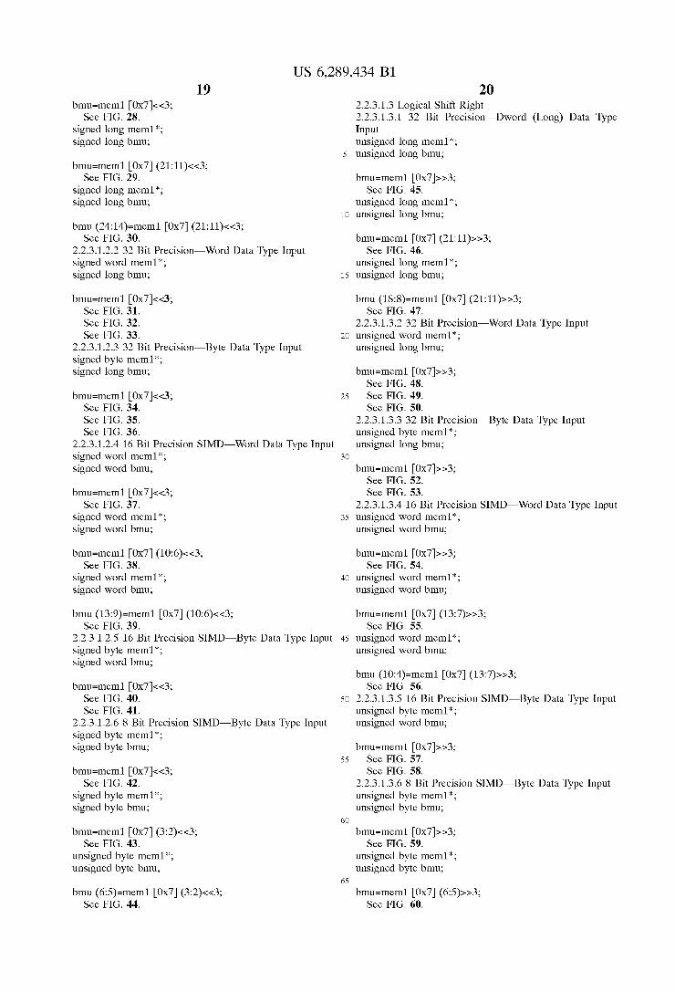
US 6,289,434 B1 19
bmu=mem10x7<<3; See FIG. 28.
signed long mem1*; signed long bmu;
bmu=mem10x7 (21:11)<<3; See FIG. 29.
signed long mem1*; signed long bmu;
bmu (24:14)=mem10x7 (21:11)<<3; See FIG. 30.
2.2.3.1.2.232 Bit Precision—Word Data Type Input signed word mem1*; signed long bmu;
See FIG. 31. See FIG. 32. See FIG. 33.
2.2.3.1.2.332 Bit Precision-Byte Data Type Input signed byte mem1*; signed long bmu;
See FIG. 34. See FIG. 35. See FIG. 36.
2.2.3.1.2.416 Bit Precision SIMD-Word Data Type Input signed word mem1*; signed word bmu;
bmu=mem10x7<<3; See FIG. 37.
signed word mem1*; signed word bmu;
bmu=mem10x7 (10:6)<<3; See FIG. 38.
signed word mem1*; signed word bmu;
bmu (13:9)=mem10x7 (10:6)<<3; See FIG. 39.
2.2.3.1.2.5 16 Bit Precision SIMD-Byte Data Type Input signed byte mem1*; signed word bmu;
See FIG. 40. See FIG. 41.
2.2.3.1.2.68 Bit Precision SIMD-Byte Data Type Input signed byte mem1*; signed byte bnu;
bmu=mem10x7<<3; See FIG. 42.
signed byte mem1*; signed byte bnu;
bmu=mem10x7 (3:2)<<3; See FIG. 43.
unsigned byte mem1*; unsigned byte bmu;
bmu (6:5)=mem10x7 (3:2)<<3; See FIG. 44.
15
25
35
40
45
50
55
60
65
20 2.2.3.1.3 Logical Shift Right 2.2.3.1.3.1 32 Bit Precision-Dword (Long) Data Type Input unsigned long mem1*; unsigned long bmu;
bmu=mem10x7->>3; See FIG. 45.
unsigned long mem1*; unsigned long bmu;
bmu=mem10x7 (21:11)>>3; See FIG. 46.
unsigned long mem1*; unsigned long bmu;
bmu (18:8)=mem10x7 (21:11)>>3; See FIG. 47.
2.2.3.1.3.232 Bit Precision—Word Data Type Input unsigned word mem1*; unsigned long bmu;
See FIG. 48. See FIG. 49. See FIG. 50.
2.2.3.1.3.332 Bit Precision-Byte Data Type Input unsigned byte mem1*; unsigned long bmu;
See FIG. 52. See FIG 53.
2.2.3.1.3.416 Bit Precision SIMD-Word Data Type Input unsigned word mem1*; unsigned word bmu;
bmu=mem10x7->>3; See FIG. 54.
unsigned word mem1*; unsigned word bmu;
bmu=mem10x7 (13:7)>>3; See FIG. 55.
unsigned word mem1*; unsigned word bmu;
bmu (10:4)=mem10x7 (13:7)>>3; See FIG. 56.
2.2.3.1.3.5 16 Bit Precision SIMD-Byte Data Type Input unsigned byte mem1*; unsigned word bmu;
See FIG. 57. See FIG. 58.
2.2.3.1.3.68 Bit Precision SIMD-Byte Data Type Input unsigned byte mem1*; unsigned byte brmu;
bmu=mem10x7->>3; See FIG. 59.
unsigned byte mem1*; unsigned byte brmu;
bmu=mem10x7 (6:5)>>3; See FIG. 60.
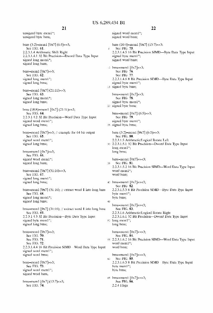
US 6,289,434 B1 21
unsigned byte mem1*; unsigned byte bmu;
bmu (3:2)=mem10x7 (6:5)>>3; See FIG. 61.
2.2.3.1.4 Arithmetic Shift Right 2.2.3.1.4.132 Bit Precision-Dword Data Type Input signed long mem1*; signed long bmu;
bmu=mem10x7->>3; See FIG. 62.
signed long mem1*; signed long bmu;
bmu=mem10x7 (21:11)>>3; See FIG. 63.
signed long mem1*; signed long bmu;
bmu (18:8)=mem10x7 (21:11)>>3; See FIG. 64.
2.2.3.1.4.232 Bit Precision-Word Data Type Input signed word mem1*; signed long bmu;
bmu=mem1 0x7da3; // example for 64 bit output See FIG. 65.
signed word mem1*; signed long bmu;
bmu=mem10x7->>3; See FIG. 66.
signed word mem1*; signed long bmu;
bmu=mem10x7 (31:16)>>3; See FIG. 67.
signed long mem1*; signed long bmu;
bmu=mem10x7 (31:16); // extract word 1 into long bmu See FIG. 68.
signed long mem1*; signed long bmu;
bmu=mem10x7 (31:16); // extract word 1 into long bmu See FIG. 69.
2.2.3.1.4.332 Bit Precision-Byte Data Type Input signed byte mem1*; signed long bmu;
See FIG. 70. See FIG. 71. See FIG. 72.
2.2.3.1.4,416 Bit Precision SIMD-Word Data Type Input signed word mem1*; signed word bmu;
bmu=mem10x7->>3; See FIG. 73.
signed word mem1*; signed word bmu;
bmu=mem10x7 (13:7)>>3; See FIG. 74.
15
25
35
40
45
50
55
60
65
22 signed word mem1*; signed word bmu;
bmu (10:4)=mem10x7 (13:7)>>3; See FIG. 75.
2.2.3.1.4.5 16 Bit Precision SIMD-Byte Data Type Input signed byte mem1*; signed word bmu;
See FIG 76. See FIG. 77.
2.2.3.1.4.68 Bit Precision SIMD-Byte Data Type Input signed byte mem1*; signed byte bnu;
bmu=mem10x7->>3; See FIG. 78.
signed byte mem1*; signed byte bnu;
bmu=mem10x7 (6:5)>>3; See FIG. 79.
signed byte mem1*; signed byte bnu;
bmu (3:2)=mem10x7 (6:5)>>3; See FIG. 80.
2.2.3.1.5 Arithmetic/Logical Rotate Left 2.2.3.1.5.132 Bit Precision-Dword Data Type Input long mem1*; long bmu;
See FIG. 81. 2.2.3.1.5.2 16 Bit Precision SIMD-Word Data Type Input word mem1*; word bmu;
See FIG. 82. 2.2.3.1.5.38 Bit Precision SIMD-Byte Data Type Input byte mem1*; byte bmu;
bmu=mem10x7k<<3; See FIG. 83.
2.2.3.1.6 Arithmetic/Logical Rotate Right 2.2.3.1.6.1 32 Bit Precision-Dword Data Type Input long mem1*; long bmu;
bmu=mem1 0x7d as 3; See FIG. 84.
2.2.3.1.6.216 Bit Precision SIMD-Word Data Type Input word mem1*; word bmu;
See FIG. 85. 2.2.3.1.6.38 Bit Precision SIMD-Byte Data Type Input byte mem1*; byte bmu;
bmu=mem1 0x7d as 3; See FIG. 86.
2.2.4 Flags

US 6,289,434 B1 23
Flags are generated by the MAU and ALU execution units. Various flags are Set depending on the results of the execution. Some flags are logical operations of other flags. This Section details the computation of these flags. Condi tional instructions use these flags to control program flow or execution. The four basic conditional flags are Carry, Negative, Zero and Overflow. All other flags are derived from these four flags. Loading the output registers of the MAU and ALU does not set these flags. These flags are only Set during an execution phase.
For logical operations only the Z flag is affected, the other flags remain unchanged. The Z flag in the PSW reflects the full 32 bits, regardless of the precision of the operation (SIMD mode). The C, N and V flags in the PSW are equivalent to the flags for the most significant word or byte of a SIMD operation. 2.2.4.1 Carry (C)
There are four carry flags for each byte of both the MAU and ALU arithmetic units. These carry flags are Set when ever there is a carry out of bits 31, 23, 15 and 7. During a multiply-accumulate operation the MAU carry flags are Set whenever there is a carry out of bits 63, 47, 31 and 15. The flags can not be individually accessed for a condition in the Software, instead all four are treated as one. In the case of a SIMD operation the individual flag bits are used in the condition, whereas in the case of a full 32 bit operation, only the most significant carry flag is used. 2.2.4.2 Negative (N)
There are four negative flags for each byte of both the MAU and ALU arithmetic units. These negative flags are set equal to bits 31, 23 15 and 7 of the result after all non multiply-accumulate operations. After a multiply accumulate operation the MAU negative flags are Set equal to bits 63, 47, 31 and 15. The accessibility of the negative flag is similar to that of the carry flag, ie, the flags are not Separately accessible for use in conditional instructions in the Software. 2.2.4.3 Zero (Z)
There are four zero flags for each byte of both the MAU and ALU arithmetic units. The Zero flags are Set in the following way. Z(3)=NOR of bits 31 to 0 during a 32 bit operation Z(3)=NOR of bits 31 to 24 during an 8 bit SIMD operation Z(3)=NOR of bits 31 to 16 during a 16 bit SIMD operation Zm(3)=NOR of bits 63 to 0 during a multiply-accumulate
operation (MAU only) Z(2)=NOR of bits 23 to 16 during 32, 16 and 8bit operations Zm(2)=NOR of bits 47 to 31 during a multiply-accumulate
operation (MAU only) Z(1)=NOR of bits 15 to 8 during 8 bit SIMD and 32 bit
operations Z(1)=NOR of bits 15 to 0 during a 16 bit SIMD operation Zm(1)=NOR of bits 31 to 0 during a multiply-accumulate
operation (MAU only) Z(0)=NOR of bits 7 to 0 during 8 and 16 bit SIMD and 32
bit operations Zm(0)=NOR of bits 15 to 0 during a multiply-accumulate
operation (MAU only) 2.2.4.4 Overflow (V)
The way the overflow flag is computed depends on the type of the two input operands, ie, whether the operands are signed, unsigned or a mix of the two. Each of the cases is explained in the following Sections. 2.2.4.4.1 Signed/Signed V=C, XOR. C. Where C=carry out of the most significant bit of the arith
metic computation and
15
25
35
40
45
50
55
60
65
24 C =carry out of the bit before the most significant
bit 2.2.4.4.2 Unsigned/Unsigned V=C, XOR. Subtract flag Where C=carry out of the most significant bit of the arith
metic computation and Subtract flag=indicates a Subtract operation if true
(hardware internal flag) 2.2.4.4.3 Signed/Unsigned V=C, XOR. S., Where C=carry out of the most significant bit of the arith
metic computation and S=most Significant bit of the signed operand or “sign
bit 2.2.45 Less Than (LT) LT-N XOR.V Where N=Negative flag V=Overflow flag
2.2.4.6 Greater Than or Equal (GE) GE=NOT. LT Where LT=Less Than flag
2.2.4.7 Less Than or Equal (LE) LE=LTOR Z. Where LT=Less Than flag, and Z=Zero flag
2.2.48 Greater Than (GT) GT=NOT LE Where LE=LeSS Than or Equal flag
2.3 MPU Data Path The data path of the MPU is configured such that all three
of the execution units described earlier can work concur rently during an execution phase. Instructions that use the execution units are known as computational instructions. This class of instructions will be explained in greater detail in the section dealing with the MPU instruction set. Com putational instructions can specify up to a maximum of four directly (or indirectly) addressable memory operands. These operands can come from anywhere in the memory map. Besides these four memory operands, computational instruc tions can also indirectly (will be explained in detail later) acceSS Various registers in the data path. The maximum number of operands (be they read or write) that can be Specified through a computational instruction is nine. The way these operands are addressed and their connection to the various inputs and outputs of the execution units is specified by an routing dictionary (again, this concept and its imple mentation will be explained in detail in a later Section).
Each execution unit is configured to have two inputs and one output. Each input of an execution unit can be connected to one of two memory ports (to access operands in the memory map, generally from the four port or Single port Sram) out of a total of four. The inputs can also be connected to their own output registers or the output registers of the execution units to the left and right of them. 2.4 Local Memory
Local memory includes the Static ram memory, dictionaries, registers and latches that are associated with each MPU. Local sram memory consists of an Instruction cache and data memory. Total memory bandwidth to local

US 6,289,434 B1 25
memory is 2.8 Gbytes/sec per MPU. All operations, besides inter-processor accesses, are executed out of and into local memory. As mentioned earlier the UMP is a memory mapped
architecture. This means that all Storage locations, be they Sram memory or registers or latches are user accessible through the memory map. Each of the local memory Sub blocks is dealt with in detail in the sections that follow and the accessibility of each of the memory blockS is explained. 2.4.1 Instruction Cache
The Instruction cache is a four-way Set-associative cache with a single index. This greatly simplifies the construction of the cache, while providing reasonably good cache per formance. The instruction cache consist of four 32 double word blocks of Single-ported Static ram, giving a total of 256 words (1.0 Kbyte) of instruction memory. Each of these blockS is Separately addressable, So that an external memory transfer could be taking place in one of the blocks while the MPU accesses instructions from another block. The cache uses a least-recently-used (LRU) replacement policy.
The tags are 11 bits wide, since each block is 32 double words long, and there are 2 LRU bits per block. The size of block fetches from external or global memory can be specified at the MPU, when replacing a block. This means that one could necessarily only fetch enough to fill half a block (32 instructions) per MPU request. There is also provision for automatic instruction pre-fetch.
In automatic instruction pre-fetch, the least recently used block is overwritten, and the LRU bits for the pre-fetched block becomes the most recently used. Pre-fetch of the Succeeding block Starts as Soon as the current block gets a hit. Pre-fetches can also be tuned by providing a trigger address (0 to 31) for the current block. An automatic pre-fetch Starts a Soon as this trigger address is accessed. Any of the instruction cache blockS can be made non
disposable, So that they are not overwritten with new data. This is useful for small terminate-and-stay-resident (TSR) type programs, which could be interrupt Service routines or Supervisory routines. This way interrupt requests and fre quently used Subroutines do not incur any overhead if the program happens to be currently executing in distant memory Space.
See FIG. 87. In the diagram above the VALID bits are not shown.
There is one VALID bit for each bank. A cache miss would occur if the tags do not match or the VALID bit is reset. On cache misses, the MPU is stalled and a DMA memory request is made if the address is to an external (outside MPU memory space) location. If it is to an internal memory location than (usually) the internal single port data ram is accessed. 2.4.1.1 Cache Replacement Algorithm
The LRU bits are modified in the following way: On a MISS, the LRU bits are all decremented by one. The
least recently used block which is “00' wraps around to be “11”; most recently used.
On a HIT, the LRU bits of the block that is hit becomes “11”, and only those blocks whose LRU bits are greater than the previous value of the block that was hit, are decremented.
2.4.2 Data Memory Data memory consists of one independently addressable
512 word Single-port Static ram blocks and one indepen dently addressable 64 word quadruple-port Static ram block, giving a total of 576 words (2.3. Kbytes) of data memory. The memory hierarchy was necessary in order to balance the need for concurrent high performance access with the cost
15
25
35
40
45
50
55
60
65
26 asSociated with multi-ported memories. Each of these blockS is mapped in an identifiable memory Space, So that appli cations can judiciously choose the various memory Spaces, depending on the number of concurrent accesses that are to be made to that locality of memory.
Five Simultaneous Dword memory accesses are allowed in a single cycle. Four of these accesses are to the quad-port memory and the fifth access can be either to an external memory Space or to the internal Single port ram. Since computational instructions can acceSS only four memory locations at a time, the fifth access can occur while manag ing the Stack (if the Stack is stored in the Single port ram) or while performing a concurrent move instruction with a computational instruction.
See FIG. 88. 2.4.3 Dictionaries MPU dictionaries are used to configure the MPU data
paths to provide an extensive instruction Set without the need for long instruction words. The dictionaries and their usage will be presented in detail in the Section on the instruction set. MPU dictionaries are part of the local MPU memory Space. Their exact location can be found in the MPU memory map diagram.
There are four MPU dictionaries and each of them is essentially single port memory. The four MPU dictionaries
C.
1. MAU dictionary 2. ALU dictionary 3. BMU dictionary 4. Routing dictionary These dictionaries are all 8 words deep and dictionary
entries are all 32 bits in length, although Some dictionaries may not have all their bits fully implemented. These dictio naries may be implemented with Srams or with addressable latches, whichever is most cost-effective. The four dictio naries are read concurrently in one clock cycle during the decode/operand-fetch phase of the execution pipeline. For non-execution access, only one read or write operation can be performed in one cycle. Thus, the four MPU dictionaries act as one single port memory during moves. 2.4.4 MPU Registers The MPU registers include both data, address, control and
Status registers. The data registers are essentially pipeline registers in the data path that hold the data through the various Stages of the execution pipeline. The data registers also hold intermediate results before they are used by the next instruction. The address registers consist of the four memory pointers and their associated indeX registers. All MPU registers are 32 bits in length, to better support the 32 bit data paths.
See FIG. 89. 2.4.4.1 Processor Status Word-PSW (R/W) 2.4.4.2 Extended Processor Status Word-EPSW (R/W)
See FIG. 90. This register contains all the basic flag bits generated by
the MAU and the ALU. As mentioned earlier, the secondary flag bits can all be derived from these basic flags.
2.4.4.3 Interrupt Register-INT (R/W) See FIG. 91. Note. The flag bits of the Interrupt register may be set
through Software to cause an interrupt. 2.4.4.4 Program Counter-PC (R/W)
See FIG. 92. Note: During program execution (Subroutine calls, jumps,
etc.), only the lower 16 bits of the PC is modified, the upper 8 bits have to be modified by a direct write to the PC.

US 6,289,434 B1 27
2.4.4.5 Stack Pointer-SP (R/W) See FIG. 93. The Stack pointer can only point to a local memory
location. This would usually be in the Single port Sram associated with the MPU. 2.4.4.6 Link Register-LR (R/W)
See FIG. 94. 2.4.4.7 Memory Pointers-MEMO, MEM1, MEM2, MEM3 (R/W)
See FIG. 95. Note: The MS Dword address bits (23 to 16) of all the
memory pointerS map to the same 8 bit register. Therefore, writes to any one of the memory pointers will always update the upper 8 bits of the address of all four memory pointers with the same value, ie, the upper 8 bits of the last memory pointer that was written. During address calculations using the memory pointers, only the lower 16 bits of the pointers are modified, the upper 8 bits have to be modified by a direct write to the pointer. 2.4.4.8 Index Registers-INDX0, INDX1, INDX2, INDX3 (R/W)
See FIG. 96. There are four 8 bit signed indexes that can be added to
each memory pointer (MEMn). Thus the index values range from +127 to -128. 2.45 MPU Memory Map
All MPU local storage is mapped into MPU memory space. The MPU memory map is shown below.
See FIG. 97A. See FIG. 97B. See FIG. 97C. See FIG. 97D.
2.5 Instruction Set 2.5.1 Introduction
The Instruction Set of the Media Processors encompasses nearly all DSP type instructions, as well as immediate data move instructions that can be used to configure the complex pipeline of the execution units. AS an example, the Multi plier could be configured to behave as four 8 bit multipliers. Each instruction is a complex 32 bit instruction that may be comprised of a number of DSP like operations.
The key characteristic of MPU “computational” instruc tions is the fact that they are interpreted instructions. This means that various instructions are encoded indirectly through a programmable instruction interpreter. This keeps the length of the instruction word to 32 bits and allows multiple instructions to be executed per clock cycle. The interpreter consists of addressable storage (which is part of the memory map) and decoder logic. The programmer must Set up the interpreter by loading up the instruction "dictio nary” with the instructions that will follow. This is what achieves the dynamic run-time reconfigurability This dic tionary may only need to be changed at the beginning of the program Segment or at the beginning of a complex inner loop operation. All other instructions have traditional micro processor or DSP characteristics. Instruction encoding will be dealt with in detail in a Subsequent Section. 2.5.2 Instruction Encoding
In all instructions the most Significant three bits decide the type and mode of the instruction. Bits 28 down to 0, are then interpreted depending on the three most significant “type' bits. 2.5.2.1 Computational Instructions
See FIG. 98. 2.5.2.1.1 Three Operation Mode
See FIG. 99. 2.5.2.1.2. Two Operation Mode
15
25
35
40
45
50
55
60
65
28 See FIG 100.
2.5.2.1.3. One Operation Mode Note. In the four port modes, a value of 00h (when
memn(30)=0) or values of 00h, 1 Ch, 1Dh, 1 Eh or 1Fh (when memn(30)=1) in any port field, indicates indirect pointer addressing for that port field. Here, the memory pointer value n is the same as the port field number. A value other than the ones mentioned above indicates a direct pointer addressing format for that port. A direct pointer address is formed by concatenating the port field value with the memory pointer memn. An offset value of 01 h, 02h and 03h concatenated with the
memory pointer memo always points to execution unit output registerS alu, bmu and mau respectively. 2.5.2.1.4 Dictionary Encoding
See FIG 101. 2.5.2.1.4.1 MAU Dictionary 2.5.2.1.4.2 ALU Dictionary
See FIG. 102. 2.5.2.1.4.3 BMU Dictionary
See FIG. 103. Note: Only 8 and 16 bit data types may be inserted with
5 bit immediate values. Unaligned data may be inserted by Specifying a shift amount and a data width through either a 10 bit immediate (most significant 5 bits specifies the data width while the least significant 5 bits specifies the shift amount) or an indirect variable at input B with the following formats. 8 Bit SIMD Mode:
See FIG 104. 16 Bit SIMD Mode: See FIG. 105. Note: Extracts can be specified through a 5 bit immediate
by setting the BMU to the right shift mode. An arithmetic shift performs a sign extended extract, whereas a logical shift performs a zero-filled extract.
For an 8 bit input data type, an immediate value of 0 extracts Byte 0 8 extracts Byte 1 16 extracts Byte 2 24 extracts Byte 3 For a 16 bit input data type, an immediate value of O extracts Word 0 16 extracts Word 1
2.5.2.1.4.4 Routing Dictionary See FIG. 106.
2.5.2.1.4.4.1 Execution Unit Port Connectivity The ALU input/output-port assignments are as follows: Input A: Port (0), Port (2) Input B: Port (1), Port (3) Output: Port (2), Port (3) The BMU input/output-port assignments are as follows: Input A: Port (0), Port (2) Input B: Port (1), Port (0) Output: Port (2), Port (3) The MAU input/output-port assignments are as follows: Input A: Port (0), Port (2) Input B: Port (1), Port (3) Output: Port (2), Port (3) Note. Input ports can be shared by Specifying the same
inputs for different execution units. Port Sharing is only done if the assembler detects two operands which are equal, ie, either they refer to the same memory pointer through indirect addressing or they have the same offset values and their memory pointers are also the same.

29 US 6,289,434 B1
2.5.2.1.4.4.2 Two Operation - Four Port Assignment Table (No shared ports)
Input A
port(O) port(O) port(2) port(O) port(O) bm/ma?al port(O) port(2) port(O) port(O) bm/ma?al
Input A
Input A
port(O) port(O) port(2) port(O) port(O) bm/ma?al port(O) port(2) port(O) port(O) bm/ma?al
Input A
port (O) port (O) port (O) port (O) bm/ma?al port (O) port (2) port (2) port (O)
port (O) port (O) port (O)
ALU
Input B Output
port(3) alu port(3) alu port(1) alu al/bm/ma port(3) al/bm/ma port(3) port(1) port(2) port(3) port(2) port(1) port(3) port(1) port(3) al?bm?ma alu al/bm/ma port(2)
ALU
Input B Output
port(1) alu port(1) port(2) port(1) alu port(1) port(2) port(1) alu al/bm/ma port(2) port(1) port(3) port(1) port(3)
MAU
Input B Output
port(3) al port(3) al port (1) al al/bm/ma port(3) al/bm/ma port(3) port(1) port(2) port(3) port(2) port(1) port(3) port(1) port(3) al?bm/ma mau al/bm/ma port(2)
Input B Output
ALU
al/bm?ma por port (1) por port (3) alu port (3) por port (1) por port (1) por port (1) alu port (1) por port (1) por
ALU
port (1) por al/bm?ma por port (1) por
(3) (2)
(2) (2) (3)
(3) (3)
(2) (3) (2)
Code Input A
4 port(2) 4 bm.fmafal 4 port(O)
9/a/b port(2) 9fafb bmima?al 9/a/b port(O) c bmima?al c port(O) 8 bmima?al
1/2/3 port(2) d/e/f port(O)
Code Input A
4 port(O) 9/a/b port(O) 4 port(O)
9/a/b port(O) 1/2/3 port(O) d/e/f port(O) c port(O) 8 bmima?al
Code Input A
4 port(2) 4 bm.fmafal 4 port(O)
9/a/b port(2) 9fafb bmima?al 9/a/b port(O) c bmima?al c port(O) 8 bmima?al
1/2/3 port(2) d/e/f port(O)
Code Input A
9/a/b port (O) 8 port (O) 4 port (O) C port (O) 9/a/b port (O) 8 bmfmafal 4 port (O) C port (O) 8 port (O)
8 port (O) 9/a/b port (O) 8 port (O)
BMU
Input B Output
port(1) bmu port(1) port(2) al/bm/ma port(3) port(1) bmu port(1) port(2) al/bm/ma port(3) port(1) bmu al?bm?ma bimu al/bm/ma port(2) port(1) port(3) port(1) port(3)
MAU
Input B Output
port(3) al port(3) al al/bm/ma port(3) al/bm/ma port(3) port(3) port(2) port(1) port(3) al?bm/ma mau al/bm/ma port(2)
BMU
Input B Output
port(1) bmu port(1) port(2) al/bm/ma port(3) port(1) bmu port(1) port(2) al/bm/ma port(3) port(1) bmu al?bm?ma bimu al/bm/ma port(2) port(1) port(3) port(1) port(3)
Input B Output
BMU
port (1) por al/bm?ma por port (1) por port (1) bmu port (1) por port (1) por port (1) por port (1) bmu port (1) por
MAU
port (1) por port (3) al
(2) (3) (2)
(3) (2) (3)
(2)
(3) (2)
ES
Code Code
Code
1/2/3 dfeff
1/2/3 dfeff
45
Code
4
Code
Code
2.5.2.1.4.4.3 Two Operation - Four Port Assignment table (Shared ports
Code
ES
1.
30

Input A
O
O
O
O
O
O
O
O
O
O
O
O
O
O
(O) (O)
(O) (O) (O) (2)
(O) (O) (O) (O)
(O) (2) (2) (O)
Input B Output
alu O
O
O
alu O
O
O
O
O
O
O
O
O
alfb O
O
O
O
O
O
O
O
al O
O
al
O
O
O
al
O
O
s
(3) (2) (3)
(2) (3)
(3) (2)
(2) (2) (3)
(3) (3)
31 US 6,289,434 B1
-continued
2.5.2.1.4.4.3 Two Operation - Four Port Assignment table (Shared ports
Code Input A
8
O
O
O
O
O
O
O
O
O
O
O
O
O
O
(O) bmfmafal
(O) (2) (2) (O) (O)
(O) (O) (O) (O) (O)
bmfmafal (O) (O) (O)
Input B Output
port (3 O
O
O
O
O
O
O
O
O
al
O
O
al
BMU
O
alfb O
O
O
O
O
O
O
O
al O
O
O
O
O
O
(2) (2) (3)
(3) (3)
(2) (3) (2)
(3) (2) (3)
(2)
Code
2.5.2.1.4.4.4. Two Operation - Three Port Assignment Table (No Sharing)
Input A
Input A
Input A
ALU
Input B Output
port(1) alu port (1) alu port(1) port(2) al?bm?ma alu al/bm/ma port(2) al?bm?ma alu port(1) port(2) al?bm?ma alu
ALU
Input B Output
port(1) alu port(1) alu port(1) port(2) al?bm?ma alu al/bm/ma port(2) al?bm?ma alu port(1) port(2) al?bm?ma alu
MAU
Input B Output
port(1) al port(1) al port(1) port(2) al?bm/ma mau al/bm/ma port(2) al?bm/ma mau port(1) port(2) al?bm/ma mau
Code Input A
4 port(O) O brmfmafal
9/a/b port(O) port(2) port(O)
5/6/7 port(O)
bmfmafal bmfmafal
Code Input A
5/6/7 port(O)
port(O) bmfmafal port(O) port(2) port(O) bmfmafal bmfmafal
Code Input A
5/6/7 port(O)
port(O) bmfmafal port(O) port(2) port(O) bmfmafal bmfmafal
BMU
Input B Output
MAU
Input B Output
al?bm/ma mau al/bm/ma port(2) al?bm/ma mau port(1) al port(1) al port(1) port(2) al?bm/ma mau port(1) port(2)
BMU
Input B Output
Note. In three port modes, only one output to a port allowed, viz., port (2)
is
Code
Code
1/2/3 dfeff 1/2/3
Code
1/2/3 dfeff 1/2/3
ES
Code
Code
Code
32

US 6,289,434 B1 33 34
2.5.2.1.4.4.5 Two Operation - Three Port Assignment Table (Shared Ports
Input A Input B Output Code Input A Input B Output Code Code
ALU BMU ES
port (2) port (1) al 4 port (O) port (1) bmu O port (O) port (1) al O port (2) port (1) bmu 4 O port (O) port (1) port (2) 8 port (O) port (1) bmu O port (O) port (1) al O port (O) port (1) port (2) 8 O port (O) al?bm?ma alu 1/2/3 port (O) port (1) port (2) 8 O port (O) port (1) port (2) 8 port (O) alfbm?ma bimu 1/2/3 port (O) al/bm/ma port (2) 9/a/b port (O) port (1) bmu O O port (O) port (1) al O port (O) al/bm/ma port (2) 9/a/b bm/ma?al port (1) port (2) 9/a/b port (O) port (1) bmu O port (O) port (1) al O bm/ma?al port (1) port (2) 9/a/b O bm/ma?al port (1) al 1/2/3 port (O) port (1) port (2) 8 port (O) port (1) port (2) 8 bm/ma?al port (1) bmu 1/2/3
ALU MAU
port (2) port (1) al 4 port (O) port (1) al O port (O) port (1) al O port (2) port (1) al 4 O port (O) port (1) port (2) 8 port (O) port (1) al O port (O) port (1) al O port (O) port (1) port (2) 8 O port (O) al?bm?ma alu 1/2/3 port (O) port (1) port (2) 8 O port (O) port (1) port (2) 8 port (O) al/bm/ma mau 1/2/3 port (O) al/bm/ma port (2) 9/a/b port (O) port (1) al O O port (O) port (1) al O port (O) al/bm/ma port (2) 9/a/b bm/ma?al port (10 port (2) 9/a/b port (O) port (1) al O bm/ma?al port (1) port (2) 9/a/b port (O) port (1) al O port (O) port (1) al O bm/ma?al port (1) port (2) 9/a/b O bm/ma?al port (1) al 1/2/3 port (O) port (1) port (2) 8 port (O) port (1) port (2) 8 bm/ma?al port (1) al 1/2/3 O
MAU BMU
port (2) port (1) al 4 port (O) port (1) O port (O) port (1) al O port (2) port (1) 4 O port (O) port (1) port (2) 8 port (O) port (1) O port (O) port (1) al O port (O) port (1) port (2) 8 O port (O) al?bm/ma mau 1/2/3 port (O) port (1) port (2) 8 O port (O) port (1) port (2) 8 port (O) alfbm?ma bimu 1/2/3 port (O) al/bm/ma port (2) 9/a/b port (O) port (1) O O port (O) port (1) al O port (O) al/bm/ma port (2) 9/a/b bm/ma?al port (1) port (2) 9/a/b port (O) port (1) O port (O) port (1) al O bm/ma?al port (1) port (2) 9/a/b O bm/ma?al port (1) al 1/2/3 port (O) port (1) port (2) 8 port (O) port (1) port (2) 8 bm/ma?al port (1) 1/2/3 O
2.5.2.1.4.4.6 Three Operation-Four Port Assignment Table The three operation 4 port combinations are as follows: (No Sharing)
ALU BMU MAU ES
In A. In B Out Code In A. In B Out Code In A. In B Out Code Code
3-1-0
p (0) p (3) p (2) c regs p (1) bmu 1/2/3 regs regs mau 5/6/7 O p (2) p. (1) p (3) c p (O) regs bmu 1/2/3 regs regs mau 5/6/7 3 p (O) p (1) p (3) 8 regs regs p (2) d/eff regs regs mau 5/6/7 O
3-0-1
p (2) p. (1) p (3) c regs regs bmu 5/6/7 p. (O) regs mau 1/2/3 1 p (O) p (1) p (2) 8 regs regs bmu 5/6/7 regs regs p (3) d/eff 1
O-1-3
regs regs alu 5/6/7 regs p (1) bmu 1/2/3 p (0) p (3) p (2) c 2 regs regs alu 5/6/7 p (O) regs bmu 1/2/3 p (2) p. (1) p (3) c 3 regs regs alu 5/6/7 regs regs p (2) d/eff p (0) p (1) p (3) 8 2
-O-3
regs p (1) alu 1/2/3 regs regs bmu 5/6/7 p. (O) p (3) p (2) c 1. regs regs p (2) d/eff regs regs bmu 5/6/7 p. (O) p (1) p (3) 8 1.

US 6,289,434 B1 37 38
-continued
2.5.2.1.4.4.7 Three Operation - Four Port Assignment Table (Shared Ports
ALU BMU MAU ES
In A. In B Out Code In A. In B Out Code In A. In B Out Code Code
regs p (1) p (2) 9/a/b p (O) p (1) bmu O regs regs p (3) d/eff 1 p (O) p (3) p (2) c p (O) p (1) bmu O regs regs mau 5/6/7 O p (O) p (1) p (2) 8 p (O) regs p (3) 9/a/b regs regs mau 5/6/7 3 p (2) p. (1) p (3) c regs regs bmu 5/6/7 p. (O) p (1) mau O 1. p (O) p (1) p (2) 8 regs regs bmu 5/6/7 p. (O) regs p (3) 9/a/b 1 regs regs alu 5/6/7 p. (O) p (1) bmu O p (O) p (3) p (2) c 2 regs regs alu 5/6/7 p. (O) p (1) bmu O p (2) p. (1) p (3) c 3
15
2.5.2.1.4.4.8 Three Operation- Three Port Assignment The three operation 3 port combinations are as follows: Table
300. 030, 003. 210, 201: 120,021. 012, 102, 111
ALU BMU MAU ES
In A. In B Out Code In A. In B Out Code In A. In B Out Code Code
p (O) p (1) p (2) 8 regs regs bmu 5/6/7 regs regs mau 5/6/7 3 O-3-O
regs regs alu 5/6/7 p (O) p (1) p (2) 8 regs regs mau 5/6/7 0 O-O-3
regs regs alu 5/6/7 regs regs bmu 5/6/7 p. (O) p (1) p (2) 8 3 2-1-0
p (0) p (1) alu O regs regs p (2) d/eff regs regs mau 5/6/7 O p (2) p. (1) alu 4. p (O) regs bmu 1/2/3 regs regs mau 5/6/7 3 regs p (1) p (2) 9/a/b p (O) regs bmu 1/2/3 regs regs mau 5/6/7 3 p (O) regs p (2) 9/a/b regs p (1) bmu 1/2/3 regs regs mau 5/6/7 O
2-0-1
p (0) p (1) alu O regs regs bmu 5/6/7 regs regs p (2) d/eff 3 p (2) p. (1) alu 4 regs regs bmu 5/6/7 p. (O) regs mau 1/2/3 1 regs p (1) p (2) 9/a/b regs regs bmu 5/6/7 p. (O) regs mau 1/2/3 1
-2-0
regs regs p (2) d/eff p (O) p (1) bmu O regs regs mau 5/6/7 3 p (O) regs alu 1/2/3 p (2) p. (1) bmu 4 regs regs mau 5/6/7 0 p (O) regs alu 1/2/3 regs p (1) p (2) 9/a/b regs regs mau 5/6/7 O regs p (1) alu 1/2/3 p (O) regs p (2) 9/a/b regs regs mau 5/6/7 3
0-2-1
regs regs alu 5/6/7 p (O) p (1) bmu O regs regs p (2) di?e/f 2 regs regs alu 5/6/7 p. (2) p. (1) bmu 4 p. (O) regs mau 1/2/3 2. regs regs alu 5/6/7 regs p (1) p (2) 9/a/b p (O) regs mau 1/2/3 2. regs regs alu 5/6/7 p (O) regs p (2) 9/a/b regs p (1) mau 1/2/3 3
0-1-2
regs regs alu 5/6/7 regs regs p (2) d/eff p (0) p (1) mau O O regs regs alu 5/6/7 p (O) regs bmu 1/2/3 p (2) p. (1) mau 4 3 regs regs alu 5/6/7 p (O) regs bmu 1/2/3 regs p (1) p (2) 9/a/b 3 regs regs alu 5/6/7 regs p (1) bmu 1/2/3 p (O) regs p (2) 9/a/b 2
-0-2
regs regs p (2) d/eff regs regs bmu 5/6/7 p. (O) p (1) mau O 2 p (2) regs alu 1/2/3 regs regs bmu 5/6/7 p (O) p (1) mau O 2 regs p (1) alu 1/2/3 regs regs bmu 5/6/7 p. (O) regs p (2) 9/a/b 1 regs p (1) alu 1/2/3 regs regs bmu 5/6/7 p. (O) regs p (2) 9/a/b 1
-1-1
p (O) regs alu 1/2/3 regs p (1) bmu 1/2/3 regs regs p (2) d/eff 0 p (O) regs alu 1/2/3 regs p (1) bmu 1/2/3 p (2) regs mau 1/2/3 0 regs p (1) alu 1/2/3 regs regs p (2) d/eff p (O) regs mau 1/2/3 1 regs p (1) alu 1/2/3 p (2) regs bmu 1/2/3 p (O) regs mau 1/2/3 1

US 6,289,434 B1 39
-continued
3OO O30 OO3, 210, 201 120 021 O12 102 111
40
ALU BMU MAU ES
In A. In B Out Code In A. In B Out Code In A. In B Out Code Code
regs p (1) alu 1/2/3 p (O) regs bmu 1/2/3 regs regs p (2) d/eff 3 p (O) regs alu 1/2/3 regs p (1) bmu 1/2/3 p (2) regs mau 1/2/3 0 regs p (1) alu 1/2/3 regs regs p (2) d/eff p (O) regs mau 1/2/3 1 regs p (1) alu 1/2/3 p (2) regs bmu 1/2/3 p (O) regs mau 1/2/3 1 regs regs p (2) d/eff p (O) regs bmu 1/2/3 regs p (1) mau 1/2/3 3 regs regs p (2) d/eff regs p (1) bmu 1/2/3 p (O) regs mau 1/2/3 2 regs regs p (2) d/eff regs p (1) bmu 1/2/3 p (O) regs mau 1/2/3 2 p (2) regs alu 1/2/3 regs p (1) bmu 1/2/3 p (O) regs mau 1/2/3 2.
2.6 Addressing 2.6.2.1.3 Pointer Indirect Addressing with Post-Modify 2.6.1 Instruction
In this architecture, program and data memory share the Same memory Space. Program memory hierarchy is built on the concept of pages. Pages are 64K Dwords (32 bit word) in size. Each MPU can directly address program memory locations automatically (ie, without any program intervention) through the least significant word (lower 16 bits) of the Program Counter (PC) within a 64KDword (32 bit word) page of memory. To address a program memory location that is off page, program intervention is required, viz, the next most significant 8 bits of the PC must be loaded. Pages are relocatable in the 64 MByte UMP address space. This is the current implementation of the UMP. In Subse quent implementations the addressable range may expand to 4 GB.
The MPU instruction space is also addressed by the Link Register (LR). The Link Register is used for subroutine returns and hardware-loop returns. The operation of these registers is explained in detail in the Section on program execution. 2.6.2. Data
Data memory hierarchy is also built on the concept of 64K Dword pages and the concept of 32 Dword blocks. Sequen tial access to the local memory Spaces is within a 64 word directly addressed block if it is to a four-port memory Space or within a 256 word sequentially addressed block if it is to a Single or multi-port memory Space. Page data memory address's are effectively the concatenation of the least significant 8, 10 or 11 bits of the memory pointers for each access, with the 5 bit direct addresses. Move instructions can Set the memory pointers. Pages are relocatable in a 64 MByte UMP address space. 2.6.2.1 Addressing Modes
All Data addressing in computational instructions is done through four fields in the least significant 20 bits of the instruction word. A maximum of four independent memory accesses are allowed per computational instruction. There may be another memory access if there is a concurrent move instruction also being executed. These may be read or write accesses. The four fields may specify either pointer concat enated direct addresses or indirect addresses, depending on the addressing mode for that field. 2.6.2.1.1 Pointer Direct Addressing
In pointer direct addressing, the address of each memory access is formed by concatenating the most significant bits of a memory pointer with the 5 bit direct address specified in the appropriate instruction field. 2.6.2.1.2 Pointer Indirect Addressing
In pointer indirect addressing, the memory pointer is directly used to address the operands.
25
35
40
45
50
55
60
65
In pointer indirect addressing with post-modify, the oper and is addressed through the memory pointer and the memory pointer is modified after the access by adding the value in the Specified indeX register to it. 2.6.2.1.4 Circular Addressing
In circular addressing, one of the memory accesses can be either a read from or a write to, a circular buffer maintained in local memory. The address pointer wraps around on Sequential reads or writes. 2.6.2.1.5 FIFO Addressing
In FIFO addressing, one of the memory accesses can be either a read from or a write to, a FIFO that is maintained in local memory. FIFO flags can be used as condition codes for program branches. 2.6.2.1.6 Bit Reversed Addressing
Bit reversed addressing is useful for implementing FFTs. 2.7 Program Execution 2.7.1 Pipeline Operation The MPU's implement a classic RISC pipeline for
instruction execution. In its most basic form, its a four phase pipeline. The four phases of the MPU pipeline are:
e IF -Instruction Fetch and Preliminary Decode e OF -Operand Fetch and Primary Decode s EX -Execute e WB -Write Back
Clock m Clock m+1 Clock m+2 Clock m+3
Instr.n IF OF EX WB Instr. n+1 IF OF EX Instr. n+2 IF OF Instr. n+3 IF
The EXECUTE part (EX) of the pipeline can be extended over multiple clocks, depending on the complexity of the operation. For example, a multiply operation would take two clock cycles to execute, whereas, an alu or shift operation would take only one clock cycle to execute. Pipelined consecutive multiply accumulates would produce a result every clock cycle, but the execution latency would be two clock cycles. Three computational operations can be started every clock cycle. The multiplier latency is maintained by the assembler, in that a non-multiply operation using the multiplier may not be started in the instruction following a multiply. On the other hand, Successive multiply-accumulate instructions are allowed.
US 6,289,434 B1 41
2.7.1.1 Description of Phases 2.7.1.1.1 Instruction Fetch Phase (IF) MPUs fetch two instructions in the same clock cycle (for
a Super-Scalar two issue pipeline.) Both instructions are Simultaneously dispatched for execution depending on the type of the instruction and availability of resources. Resources include execution units and memory access cycles. There can only be five local memory accesses in any one clock cycle. Four of these accesses are to the four port memory while the fifth one can be to either the local single port memory or to an external memory location. Most Branch instructions can be executed in parallel with com putational instructions. Instructions that cannot be executed in parallel are held till the next decode phase. There is only a two instruction buffer in each MPU (for two issue Super Scalar operation), i.e., the MPU can only look ahead two instructions. Speculative fetching of branch target instruc tions is also performed, which, as is shown in the Section on branching, greatly improves processor performance. In the IF phase a preliminary decode of the instruction is done, Such as determining the instruction type, ie computational or non-computational, etc. 2.7.1.1.2. Operand Fetch and Decode Phase (OF)
Data integrity over consecutive instruction writes and operand fetches from the same location is maintained by assembler or compiler (Software) pipelining of the write back data. Computational instructions can fetch up to four memory operands in each phase. Since only four memory accesses can be made by a computational instruction in one cycle, writes from previous instructions have priority over reads from the current instruction. When Such a contention is encountered, the MPU is stalled until the the next cycle. Instruction decode is accomplished through direct decode of the opcode and type bits in the instruction word, and indirect decode through the dictionaries. 2.7.1.1.3 Execute Phase (EX)
During the execute phase, the address computations with the indeX registers and the execution unit operations are performed. Results from the current execute phase are available to the next instruction's execute phase through the alu, mau and bmu output registers and to the execute phase after that through the alureg, bmureg and maureg Output registers. 2.7.1.1.4 Writeback Phase(WB)
In the writeback phase, the results of the operations are written to memory. Write memory accesses always have priority over reads. 2.7.1.2 Branch Instructions
In this section we will deal in detail with all the pipelining issueS associated with program flow instructions. Each Step of the pipeline alongwith all that is happening will be explained.
Note: What follows are details for a single issue pipeline only. 2.7.1.2.1 Unconditional Direct Branch goto long direct address,
Phase Operations
IF preliminary decode: PC (15:0) = 16 bits of immediate long address in instruction;
OF null; EX null; WB null;
2.7.1.2.2 Conditional Direct Branch
5
15
25
35
40
45
50
55
60
65
42 if (condition) goto long direct address;
Phase Operations
IF preliminary decode: conditional direct goto flag = TRUE.; if (prediction bit) PC (15:0) = 16 bits of immediate long address in instruction; PC Buffer = PC + 1:
else PC = PC + 1; PC Buffer = 16 bits of immediate long address in instruction;
if (conditional direct goto flag) if (condition .xor-prediction) PC = PC Buffer; IF = NULL.; (nullify current (wrong) instruction fetch)
null: null:
OF
EX WB
2.7.1.2.3 Unconditional In-Direct Branch goto (amemnfive bit address); // any of mem0,mem1, mem2,mem3 allowed
goto (GmemShort address;
Phase Operations
IF preliminary decode; indirect goto flag = TRUE;
OF if (indirect goto flag) fetch operand; PC = operand; IF = NULL.; nullify current (wrong) instruction fetch)
EX null; WB null;
2.7.1.2.4 Conditional In-Direct Branch if (condition) goto (amemnfive bit address); // mem0, mem1,mem2,mem3
if (condition) goto (a memShort address;
Phase Operations
IF preliminary decode: conditional indirect goto flag = TRUE.; PC = PC + 1;
OF if (conditional indirect goto flag) fetch operand; if (condition) then PC = operand; IF = NULL.;
EX null; WB null;
2.7.1.2.5 Unconditional Direct Subroutine Branch call long direct address,
Phase Operations
IF preliminary decode: if (count valid flag) immediately
direct call flag = TRUE.: indirect “for instruction if (for count l= 0) TOS (31) = TRUE.;
else TOS (31) = .FALSE.:
II always valid except when
If following an

US 6,289,434 B1 43
-continued
Phase Operations
if (for loop flag &&. (for end addr = = PC (6:0)) &&. (for count = 0)) TOS (30:0) = LNK:
else TOS (30:0) = PC + 1:
for loop flag = .FALSE.; PC = immediate long address in instruction; SP = SP - 1;
tos valid flag = TRUE. else // previous instruction was an indirect “for”
IF = NULL; // nullify instruction fetch OF if (direct call flag && IF = NULL.)
(SP) = TOS; // TOS is Top Of Stack cache register null: null:
EX WB
2.7.1.2.6 Conditional Direct Subroutine Branch
if (condition) call long direct address;
Phase Operations
IF preliminary decode: if (count valid flag)
conditional direct call flag = TRUE.; if (prediction bit)
prediction flag = TRUE.; if (for loop flag &&. (for end addr = = PC (6:0)))
if (for count = 0) TOS (31) = TRUE.; TOS (30:0) = LNK: PC Buffer (31) = TRUE.: PC Buffer (30:0) = LNK:
else TOS (31) = .FALSE.: TOS (30:0) = PC + 1: PC Buffer (31) = .FALSE.: PC Buffer (30:0) = PC + 1:
// branch likely
else TOS (31) = for loop flag: TOS (30:0) = PC + 1: PC Buffer (31) = for loop flag: PC Buffer (30:0) = PC + 1:
PC = immediate long address in instruction; SP = SP - 1; tos valid flag = TRUE. for loop flag = .FALSE.;
else prediction flag = .FALSE.; if (for loop flag &&. (for end addr = = PC (6:0)))
if (for count = 0) PC (30:0) = LNK:
else PC (30:0) = PC + 1:
// branch unlikely
else PC (30:0) = PC +1;
PC Buffer (31) = .FALSE.: PC Buffer (30:0) = immediate long address in instruction;
else IF = NULL.; OF if (conditional direct call flag && IF = NULL.)
if (prediction flag) (SP) = TOS; if (condition) pop flag = TRUE.; SP = SP + 1; tos valid flag = .FALSE.;
else if (condition) TOS (31) = for loop flag: TOS (30:0) = PC; push flag = TRUE.; SP = SP - 1: tos valid flag = TRUE.;
if (condition .xor-prediction flag) // incorrectly predicted
15
25
35
40
45
50
55
60
65
44
-continued
Phase Operations
PC = PC Buffer; for loop flag = PC Buffer (31); IF = NULL; If nullify current (wrong) instruction fetch
if (pop flag) TOS = (SP); pop flag = .FALSE.; tos valid flag = TRUE.;
if (push flag) (SP) = TOS; push flag = .FALSE.;
null:
EX
2.7.1.2.7 Unconditional In-direct Subroutine Branch
call (amemnfive bit address); // any of mem0,mem1, mem2,mem3 allowed
call (a memShort address;
Phase Operations
IF preliminary decode: if (count valid flag)
in-direct call flag. TRUE.; if (for count = 0) TOS (31) = TRUE.;
else TOS (31) = .FALSE.:
if (for loop flag &&. (for end addr = = PC (6:0)) &&. (for count = 0)) TOS (30:0) = LNK:
else TOS (30:0) = PC +1;
for loop flag = .FALSE.; SP = SP - 1; tos valid flag = TRUE.;
else IF = NULL.;
OF if (indirect call flag && IF = NULL.) fetch operand; (SP) = TOS; PC = operand; If operand has branch address
IF = NULL.; (nullify current (wrong) instruction fetch) null: null:
EX WB
2.7.1.2.8 Conditional In-direct Subroutine Branch
if (condition) call (Gmemnfive bit address); // mem0, mem1,mem2,mem3
if (condition) call (GmemShort address;
Phase Operations
IF preliminary decode: if (count valid flag)
conditional indirect call flag = TRUE.; if (prediction bit)
prediction flag = TRUE.; if (for loop flag & & (for end addr = = PC (6:0)))
if (for count = 0) TOS (31) = TRUE.; TOS (30:0) = LNK: PC Buffer (31) = TRUE.: PC = LNK:
else TOS (31) = .FALSE.: TOS (30:0) = PC + 1: PC Buffer (31) = .FALSE.: PC = PC + 1;
// branch likely

US 6,289,434 B1 45 46
if (condition) return; -continued
Phase Operations else s Phase Operations TOS (31) = for loop flag: IF preliminary decode: TOS (30:0) = PC + 1: conditional return flag = TRUE.; PC Buffer (31) = for loop flag: if (prediction bit) PC = PC + 1; prediction flag = TRUE.;
SP = SP - 1; PC Buffer (31) = for loop flag: tos valid flag = TRUE.; 1O PC Buffer (30:0) = PC (30:0) + 1: for loop flag = .FALSE.; if (tos valid flag)
else // branch unlikely PC = TOS; prediction flag = .FALSE.; for loop flag = TOS (31); if (for loop flag &&. (for end addr = = PC (6:0))) else
if(for count = 0) PC = operand; ff from stack PC (30:0) = LNK: 15 for loop flag = operand (31);
else tos valid flag = .FALSE.; PC (30:0) = PC + 1: SP = SP + 1;
else else PC (30:0) = PC +1; prediction flag = .FALSE.;
PC Buffer (31) = .FALSE.: PC = PC + 1; else 2O if (tos valid flag)
IF = NULL.; PC Buffer = TOS: OF if (conditional indirect call flag && IF = NULL.) else
fetch operand; PC Buffer = operand; ff from stack if (prediction flag) OF if (conditional return flag)
(SP) = TOS; if (condition .xor-prediction) if (condition) PC = PC Buffer; pop flag = TRUE.; 25 for loop flag = PC Buffer (31); SP = SP + 1; IF = NULL.; If nullify current (wrong) instruction tos valid flag = .FALSE.; fetch
else if (prediction flag) if (condition) fetch (SP); TOS (31) = for loop flag: if (condition) TOS (30:0) = PC (30:0); 3O SP = SP-1; push flag = TRUE.; tos valid flag = TRUE.; // always set true, although IF SP = SP - 1: Overrides setting tos valid flag = TRUE.; else
if (condition) TOS = (SP); PC = operand; else
if (condition .xor-prediction flag) 35 if (condition) for loop flag = PC Buffer (31); SP = SP +1; IF = NULL.; If nullify current (wrong) instruction tos valid flag = .FALSE; fetch to fix TOS pop flag = TRUE;
EX if (pop flag) EX if (pop flag) TOS = (SP); TOS = (SP); pop flag = .FALSE.; 40 tos valid flag = TRUE.; tos valid flag = TRUE.; pop flag = .FALSE;
if (push flag) WB null: (SP) = TOS; push flag = .FALSE.;
WB null; 2.7.1.3 Loop Instructions 45 2.7.1.3.1 Direct Loop
2.7.1.2.9 Unconditional Return for (n) // where 0>nk=256 return,
50 Phase Operations Phase Operations IF preliminary decode:
for direct flag = TRUE.; IF preliminary decode: TOS (31) = for loop flag:
return flag = TRUE. TOS (30:24) = for end addr; if (tos valid flag) 55 if(count valid flag) PC = TOS; TOS (23:16) = operand; //loop count from memory, previous for loop flag = TOS (31); loop is indirect
else else PC = operand; ff from stack TOS (23:16) = for count; for loop flag = operand (31); TOS (15:0) = LNK:
tos valid flag = .FALSE.; tos valid flag = TRUE. SP = SP + 1; 60 for end addr = 7 lsbs of immediate end address in instruction
OF if (return flag) word; TOS = (SP); for count = 8 bits of immediate (loop count - 1) in tos valid flag = TRUE.; instruction word;
EX null: for loop flag = TRUE.; WB null: count valid flag = TRUE.;
65 LNK = PC = PC + 1: SP = SP - 1;
2.7.1.2.10 Conditional Return

US 6,289,434 B1 47
-continued
Phase Operations
OF if (for direct flag) (SP) = TOS;
EX null; WB null;
2.7.1.3.2 Indirect Loop for (Gmemnfive bit address); // mem0,mem1, mem2, mem3
for (GmemShort address);
Phase Operations
IF preliminary decode: for indirect flag = TRUE., TOS (31) = for loop flag: TOS (30:24) = for end addr; if (count valid flag) TOS (23:16) = for count operand; // from memory, previous loop is indirect
else TOS (23:16) = for count;
TOS (15:0) = LNK: tos valid flag = TRUE. for end addr = 7 lsbs of immediate end address in instruction word; for loop flag = TRUE.; count valid flag = .FALSE.;
SP = SP - 1; OF if (for indirect flag)
fetch operand; for count = 8 bits of immediate (loop count - 1) in operand; count valid flag = TRUE.; (SP) = TOS;
EX null; WB null;
2.7.1.3.3 Loop operation The following loop pipeline is only a template of loop
operation. Pipeline register assignments Specifically described for various other instructions will always override the assignments shown below. In the case of the SP, assign ments in the other instructions would nullify (if opposing) the ones below.
Phase Operations
IF if (for loop flag) if (for end addr = = PC (6:0))
if (count valid flag) if (for count = 0)
for count = for count - 1: for loop flag = TRUE.;
else if (!tos valid flag)
for loop flag = operand (31); If operand fetched from stack for end addr = operand (30:24); for count = operand (23:16); LNK = operand (15:0);
else for loop flag = TOS (31); for end addr = TOS (30:24); for count = TOS (23:16); LNK = TOS (15:0);
PC = PC + 1;
1O
15
25
35
40
45
50
55
60
65
48
-continued
Phase Operations
OF
SP = SP + 1; pop flag = TRUE. tos valid flag = .FALSE.;
else PC = PC; IF = NULL.; // nullify current instruction fetch and repeat
else PC = PC + 1;
else PC = PC + 1;
if (pop flag) TOS = (SP); pop flag = .FALSE.; tos valid flag = TRUE;
2.7.1.4 Move Instructions
2.7.1.4.1 Immediate Data Move
memnfive bit address. W =Sixteen bit immediate data; // n=0,1,2,3
memShort address. W=Sixteen bit immediate data; w=0,1
Phase Operations
IF
OF
EX
preliminary decode:
if (INSTR (25:24) = 10) wr flag = .FALSE.;
else wr flag = TRUE.;
if (INSTR (25:22) = 00x1) MV Buffer (31:15) = INSTR (23); II sign bit MV Buffer (14:0) = INSTR (14:0);
else if (INSTR (24) = 0) MV Buffer (31:16) = MV Buffer; MV Buffer (15:0) = INSTR (23) (14:0);
else if (INSTR (24) = 1) MV Buffer (31:16) = INSTR (23) (14:0); MV Buffer (15:0) = MV Buffer;
if (pointer direct write) // offset = 00h. P3WR ABuffer (7:0) = memm (7:0); if (post index // memm (30) = 1 mem = mem + im; // offset = 1Ch (miO), 1 Dh (mi1), 1Eh (mi2), 1Fh (mi3)
else if (pointer offset write) P3WR ABuffer (7:5) = memm (7:5); P3WR ABuffer (4:0) = INSTR (19:15); // 5 LSB short address (offset)
else if (short direct write) P3WR ABuffer (6:0) = INSTR (21:15); P3WR ABuffer (7) = “0”;
if (pointer direct write && wr flag) // offset = 00h (mem (29:8) P3WR ABuffer (7:0)) = MV Buffer;
else if pointer offset write && Wr flag) (mem (29:8) P3WR ABuffer (7:0)) = MV Buffer;
else if (short direct write & & Wr flag) (P3WR ABuffer (7:0) + base = MV Buffer;
null:
2.7.1.4.2 Direct Address Move with Immediate Burst Length
memnfive bit address=ten bit direct address; // Single transfer
ten bit direct address=memnfive bit address, 27; // burst 27

US 6,289,434 B1 49
Phase Operations
IF
OF EX WB
2.7.1.4.3 Direct Address Move with Indirect Burst Length memnfive bit address=ten bit immediate address,
preliminary decode: if (dma length = 0 (dma length = 1 && dma indirect flag) dma indirect flag = .FALSE.; dma rd flag = TRUE.; dma length = INSTR (14:10); // immediate burst length from instruction length valid flag = TRUE.; PC = PC + 1;
else IF = NULL;
null: null: null:
memo offset; ten bit immediate address=memnfive bit address, memo offset;
Phase Operations
IF
OF
EX WB
preliminary decode: if (dma length = 0 (dma length = 1 && dma indirect flag)) dma rd flag = TRUE.; length valid flag = .FALSE.; PC = PC + 1;
else IF = NULL.;
fetch operand (burst length); dma indirect flag = TRUE.; dma length = operand (4:0); // burst length - 1 length valid flag = TRUE.; null: null:
2.7.1.4.4 MPU DMA Operation
Phase Operations
OF if (dma rd flag) if (dma indirect flag && (dma length = 0 &&. length valid flag)) dma Wr flag = .FALSE.;
else if (long direct address to short address) If direct or indirect short address MV Buffer = (ten bit long direct address + base);
else MV Buffer = (mem);
if (pointer direct write) // offset = 00h, 1Ch, 1Dh, 1Eh, 1 Fh P3WR ABuffer (7:0) = memm (7:0);
else if (pointer offset write) P3WR ABuffer (7:5) = memm (7:5); P3WR ABuffer (4:0) = INSTR (19:15); // 5 LSB short address (offset)
else if (short direct write) P3WR ABuffer (6:0) = INSTR (21:15); P3WR ABuffer (7) = “0”;
else if (long direct write) if (first transfer) P3WR ABuffer (7:0) = INSTR (7:0);
else P3WR ABuffer (7:0) = LADR ABuffer (7:0);
dma wr flag = TRUE.; if (post index) // memm (30) = 1, offset = 1 Ch (miO), 1Dh (mi1),
ff offset = OOh
15
25
35
40
45
50
55
60
65
SO
-continued
Phase Operations
EX
mem= memn + im; if if (first transfer) then LADR ABuffer (9:0) = ten bit long direct address + 1;
else LADR ABuffer (9:0) = LADR ABuffer (9:0) + 1:
if (dma length = 0 &&. (NOTdma indirect flag)) (dma indirect flag & & dma length = 1)) dma rd flag = .FALSE.;
else dma rd flag = TRUE.;
if (dma length = 0) dma length = dma length - 1; II assignment is overridden by move instr.
1Eh (mi2), 1 Fh (mi3)
if(dma Wr flag) if (pointer direct write) // offset = 00h. (mem (29:8) P3WR ABuffer (7:0)) = MV Buffer;
else if (pointer offset write) (mem (29:8) P3WR ABuffer (7:0)) = MV Buffer;
else if (short direct write) (P3WR ABuffer (7:0) + base) = MV Buffer;
else if (long direct write) (LADR ABuffer (9:8) P3WR ABuffer (7:0) + base) = MV Buffer;
dma wr flag = .FALSE.; // always set false, although OF overrides setting
2.7.1.5 Miscellaneous Instructions 2.7.1.5.1. No-operation
Phase Operations
IF preliminary decode; OF null; EX null; WB null;
2.7.1.6 Computational Instructions 2.7.1.6.1 Non multiply instruction
memD Ox23 = alu & memD mask, bmu = bmu << 16: Phase Operations
IF preliminary decode: PC = PC + 1; fetch operands; if (post index memn & & read from mem. & & limmediate value) mem= memn + im;
read dictionaries; decode dictionary entries; perform computational operations; if (mau operation) MAU = result of operation;
if (alu operation) ALU = result of operation;
if (bmu operation) BMU = result of operation;
if (agu operation) MEMin = MEMn+ im:
if (output = (MAU, ALU or BMU registers) write appropriate output register to memory;
OF
EX

US 6,289,434 B1 S1
-continued
memo Ox23 = alu & memD mask, bmu = bmu << 16: Phase Operations
if (post index memn & & write to mem) mem= mem + im;
2.7.1.6.2 Multiply instruction
mau = alu * memo mask: Phase Operations
IF preliminary decode: PC = PC + 1;
OF fetch operands; read dictionaries; decode dictionary entries;
EX1 perform carry-save addition of multiply operation; mau carry = carry output of carry-save addition; mau save = save output of carry-save addition;
EX2 if (mau operation) MAU = mau carry + mau save; (carry propagate addition)
WB if (output = (MAU, ALU or BMU registers) write appropriate output register to memory;
2.7.1.7 Interrupt Handling 2.7.2 Branching and Looping
Speculative fetching of branch target instructions allows Zero-Overhead unconditional branches and Zero cycle or Single cycle conditional branches (depending on whether the branch is taken or not). Static branch prediction is provided in the instruction word, which if used judiciously can consistently provide Zero-Overhead conditional branching. Static branch prediction is used to Selectively fetch operands So that they are ready for the execution units.
Zero-Overhead loops are implemented using an 8bit Loop Count/Condition Register (LCR) and a 16 bit Link Register (LR). The LCR is used to maintain the current loop count or the loop termination condition code. Loops can have a maximum count of 256. The loop terminates when this count reaches Zero or the termination condition is met. The LR contains the address of the first instruction of the current loop. The loop count can be an immediate value in the loop instruction or a value in a memory location. The last instruction in the loop is specified by its addresses least Significant byte, and is included in the loop instruction word. 2.7.3 Subroutines, Interrupts and Nested Loops
Subroutine calls, interrupts and nested loops all make use of a user definable Stack. This Stack can be defined anywhere in the memory Space, preferably in local memory, and cannot be more than 256 locations deep. The Stack Pointer (SP) points to the top of this stack. When a subroutine call, interrupt or nested loop is encountered in the instruction Stream, the return address is loaded into the Link Register (LR), and the address in the LR along with the value in the LCR is pushed onto the stack. The Stack Pointer is incre mented. On encountering a return instruction, the current value in the LR is used as the target address, the Stack is popped and that new address from the Stack is loaded into the LR. This scheme delivers Zero-overhead branches on unconditional Subroutine calls, nested loops and interrupts. 2.7.4 Power-Up Sequence 2.8 Interrupts On receiving an interrupt request, the MPU disables
interrupts, loads the Link Register with the current value of the Program Counter, completes execution of all the instruc
15
25
35
40
45
50
55
60
65
52 tions in the pipeline and branches to the interrupt target address. The interrupt target address is a fixed decode of the interrupt Specification bits. The interrupt targets are mapped into the MPU memory space. 2.9 Interface
Data transfer into and out of the MPU is through the block communication protocol. The Block communication Speci fication can be found in the chapter on UMP architecture. Block data transfers into and out of the MPU can proceed independent of MPU data path operation. That is, a burst move using a move instruction is basically a DMA transfer and can proceed in parallel with MPU instruction execution. Only one read or write DMA transfer operation can be going on at a time. If another move instruction follows, or the instruction cache makes a request to fill the cache, then the current transfer has to complete before the Second one can proceed. While the second transfer is waiting the MPU will stall. During a DMA transfer, the MPU transfer bit in the PSW is set. There are two bits, one for the MPU as a master and the other for the MPU as a target. Once the transfer has been completed, the appropriate bit is reset.
3. Memory Management Unit 3.1. Overview The Memory Management Unit (MMU) is responsible for
all global data transfer operations. This includes inter processor transfers, transferS to and from external memory, transfers between local memory units, etc. The MMU arbi trates multiple transfer requests and grants accesses to available parallel data transfer resources. For example, the MMU could be reading external memory for one MPU while it was coordinating and executing three other Separate parallel memory data transfers between three MPU pairs. Internal or external memory transferS take place based on the memory address given by the requesting Source. This is also true for direct memory to processor or processor to processor data transferS Since every resource on chip is memory mapped. 3.2 MMU Operation 3.2.1 Arbitration
There are a total of 16 request ports to the MMU. These requests are Serviced based on available communication resources, pre-assigned priorities, time of request and round robin schemes. In the current implementation of the UMP, there are direct data transfer paths to all the peripheral interface blockS. Each of these interfaces has a Supervisor assigned priority level for data transfers. The MPUs also have priority levels assigned for a particular task running on them. Again, these priority levels are assigned by the Super visor. There are a total of eight priority levels. These priority levels range from 000 (lowest priority) to 111 (highest priority). For example, the CDI (CRT display interface) would generally be set to the highest priority level (111) Since memory accesses to the frame buffer in local memory cannot be interrupted for too long without breaking up the display. The MPUs are assigned any of the lower four priority levels, ie, levels 0 to 3. This means that it is implied that the most significant bit of an MPU priority level is always 0. Therefore, only the two least significant bits of the priority are stored and transferred by the MPUs. 3.2.2 Privilege
Privilege levels (Supervisor or user) are also transmitted with the transfer requests. AS it Stands writes to Supervisory memory Segments, words orbits by user transfer requests go through without the data being actually written. There is currently no trap generated on Such acceSS Violations. 3.2.3 Resource Allocation The MMU routes data transfer requests through it. It
decodes the top bits of the transfer address and routes the
US 6,289,434 B1 S3
data to the appropriate memory Segment. If the Segment is currently not in use than its lock bit is Set and the transfer proceeds. If the lock bit is Set, meaning that another transfer to the same memory Segment is taking place, than the MMU does nothing, ie, RDY to the transfer initiator (master) remains deasserted. When the previous transfer completes, than the current transfer is forwarded, and the MMU waits for the RDY from the target, which it then passes back to the master. Communication between the MPUs and the MPUs and peripherals is through a four lane data highway. The lanes of the highway are basically data transfer resources. Lanes are assigned depending on availability. When only one lane is available for multiple transfer requests, than arbitration rules apply. 3.3 DMA Engine
The MMU includes a DMA engine that can be pro grammed to automatically transfer bursts of data between two memory locations. The DMA registers can be pro grammed to perform 2-D data transfers such as in BitBLT operations. Either the Source or destination address can be designated to be outside the UMP address space, but not both. When one of the addresses is outside UMP memory Space, then the DMA proceeds by concatenating the 26 bits of the external address with the 6 extension bits of the PCI External Address Pointer. 3.3.1 DMA Registers 3.3.1.1 Source Byte Address Register-SAR (R/W)
This address provides up to 64 MB addressing capability. Actual implementation may be leSS.
See FIG 107. 3.3.1.2. Destination Byte Address Register-DAR (R/W)
This address provides up to 64 MB addressing capability. Actual implementation may be less.
See FIG. 108. 3.3.1.3 Transfer Size Register-TSR (R/W)
This register Specifies the size of the data transfer in 2-D. See FIG. 109.
3.3.1.4 Source and Destination 2-D Warp Factor Register WARP (R/W)
This register specifies the size of the offset that must be added to the Source and destination addresses to find the Starting address at each new line for linear memory.
See FIG. 110. 3.3.1.5 DMA Command Register-DMAC (R/W)
This is the DMA command register. Writing this register initiates a DMA operation. therefore, it should be written last.
See FIG. 111. 3.4 Memory Map
See FIG. 112.
4. Event Timer Unit 4.1. Overview
The Event Timer Unit has been provided to allow syn chronization between the various media Streams. This unit has two 32 bit (pipelined) timers, each of which can be split into two 16 bit timers providing a total of up to four 16 bit timers that are independently addressable and Settable. The timers are key in maintaining, transporting and processing various media Stream packets So that they keep in lock Step with their time stamps and each other. All MPUs, regardless of the type of media Stream they are processing, be they audio, Video, graphics, etc., refer to the Event Timer Unit (ETU) to control their processing rate, data fetches, data writes, etc. This can be done by directly accessing the memory site of the ETU or through a system of interrupts and interrupt handling routines.
15
25
35
40
45
50
55
60
65
S4 4.1.1 Detailed Description The four timers are specified as timers 0, 1, 2 and 3. All
four timers are essentially 16 bit down counters. When used in 32 bit mode, the least significant 16 bits of the timer (timers 0 or 2 as the case may be) is used as a Scaling counter. The process of Specifying timers 0 or 2 as Scaling counters, will Set the respective timers to operate in 32 bit mode. There are interrupt bits for each of the timers to Specify whether they should generate an interrupt or not when they have counted down to zero. The timers can be programmed to work in Start-Stop mode or continuous-loop mode. In the Start-Stop mode of operation the value from the period register is loaded into the counter and the counter counts down to Zero and Stops. It generates an interrupt if the respective interrupt bit is Set. It then staySat Zero indefinitely or until another start command is given. In the continuous loop mode, the counter re-loads itself from its own period register when the count reaches Zero and Starts all over again. This goes on indefinitely, until the Stop command is given through the control register. 4.1.2 Register Descriptions 4.1.2.1 Timer Status and Control Register TSCR (R/W)
See FIG. 113. 4.1.2.2 Timer Period/Scale Registers-TPS0, TP1, TPS2, TP3 (R/W)
See FIG. 114. 4.1.2.3 Timer Counters TCO, TC1, TC2, TC3 (R/W)
See FIG. 115. 4.1.3 Memory Map
See FIG. 116.
5. Miscellaneous 5.1 Peripheral connectivity The peripheral interface units are the media links of the
Unified Media Processor. They input and output various media types to the UMP for processing. These units have very Specific definitions as to the format and Synchronization of the various media types. The units that have been pro Vided cover most current popular media interfaces. These include the PCI and AGP local bus interfaces for commu nicating with the host CPU in a PC based system. The Video Capture interface is provided for use in Video capture and Video telephony applications, while the Auxiliary Serial/ Parallel interface may be used for capturing and playing back telephone conversations or providing CD quality Sur round Sound for games, movies and music. It can also be used for telecommunications, as in Video and audio telephony, by connecting with an Audio/Modem codec. In this case, the UMP, concurrently with other types of processing, also performs the modem function. Finally, the CRT Display interface provides the sync and video signals for displaying true-color gamma-corrected 24 bit RGB images on a high resolution computer monitor or television Set.
The Unified Media Architecture introduces the concept that media Streams can be dealt with in a homogeneous and consistent manner without the need for Specialized archi tectures. The underlying principle is one of high Speed compute intensive data processing. By dealing with these various simultaneous media Streams in a homogeneous manner, Synchronization and interactivity issues are greatly Simplified, thereby leading to a simple architecture that can operate at a very high Speed. The underlying principle behind the media interfaces is
that the nature of the interface and its peculiarities is hidden from Software running on the MPUs. All communication between the MMU and the Interfaces is at the system clock. The interfaces fifo the data internally and process the data at

US 6,289,434 B1 SS
their own clock Speeds. All communication between the interfaces and the MMU is through memory reads and writes. This is possible Since all peripherals are memory mapped. 5.2 Event Timing
The Event Timer Unit has been provided to allow syn chronization between the various media Streams. This unit has two 32 bit (pipelined) timers, each of which can be split into two 16 bit timers providing a total of up to four 16 bit timers that are independently addressable and Settable. The timers are key in maintaining, transporting and processing various media Stream packets So that they keep in lock Step with their time stamps and each other. All MPUs, regardless of the type of media Stream they are processing, be they audio, Video, graphics, etc., refer to the Event Timer Unit (ETU) to control their processing rate, data fetches, data writes, etc. This can be done by directly accessing the memory site of the ETU or through a system of interrupts and interrupt handling routines.
I claim: 1. An apparatus for processing data, comprising: an addressable memory for Storing the data, and a plu
rality of instructions, and having a plurality of input/ outputs, each Said input/output for providing and receiving at least one Selected from the data and the instructions,
a plurality of media processing units, each media pro cessing unit having an input/output coupled to at least one of the addressable memory input/outputs and com prising: a multiplier having a data input coupled to the media
processing unit input/output, an instruction input coupled to the media processing unit input/output, and a data output coupled to the media processing unit input/output;
1O
15
25
S6 an arithmetic unit having a data input coupled to the media processing unit input/output, an instruction input coupled to the media processing unit input/ output, and a data output coupled to the media processing unit input/output;
an arithmetic logic unit having a data input coupled to the media processing unit input/output, an instruc tion input coupled to the media processing unit input/output, and a data output coupled to the media processing unit input/output, capable of operating concurrently with at least one Selected from the multiplier and arithmetic unit; and
a bit manipulation unit having a data input coupled to the media processing unit input/output, an instruc tion input coupled to the media processing unit input/output, and a data output coupled to the media processing unit input/output, capable of operating concurrently with the arithmetic logic unit and at least one Selected from the multiplier and arithmetic unit,
each of the plurality of media processors for performing at least one operation, Simultaneously with the performance of other operations by other media processing units, each operation comprising:
receiving at the media processor input/output an instruc tion from the memory;
receiving at the media processor input/output data from the memory;
processing the data responsive to the instruction received to produce at least one result, and
providing at least one of the at least one result at the media processor input/output.
k k k k k