Embed Size (px)
Citation preview

Ultralow Noise, 200 mA Linear Regulator
Data Sheet ADM7160
FEATURES PSRR performance of 54 dB at 100 kHz Ultralow noise independent of VOUT
3 µV rms, 0.1 Hz to 10 Hz 9.5 µV rms, 0.1 Hz to 100 kHz 9 µV rms, 10 Hz to 100 kHz 17 µV rms, 10 Hz to 1 MHz
Low dropout voltage: 150 mV at 200 mA load Maximum output current: 200 mA Input voltage range: 2.2 V to 5.5 V Low quiescent and shutdown current Initial accuracy: ±1% Accuracy over line, load, and temperature: −2.5%/+1.5% 5-lead TSOT package and 6-lead LFCSP package
APPLICATIONS ADC/DAC power supplies RF, VCO, and PLL power supplies Post dc-to-dc regulation
APPLICATION CIRCUIT
Figure 1. ADM7160 Powering a 16-Bit/18-Bit ADC
GENERAL DESCRIPTION The ADM7160 is an ultralow noise, low dropout linear regulator that operates from 2.2 V to 5.5 V and provides up to 200 mA of output current. The low 150 mV dropout voltage at 200 mA load improves efficiency and allows operation over a wide input voltage range.
Using an innovative circuit topology, the ADM7160 achieves ultralow noise performance without the need for a bypass capacitor, making the device ideal for noise-sensitive analog front-end and RF applications. The ADM7160 also achieves ultralow noise performance without compromising PSRR or transient line and load performance.
Current-limit and thermal overload protection circuits prevent damage under adverse conditions. The ADM7160 also includes an internal pull-down resistor on the EN input.
The ADM7160 is specifically designed for stable operation with tiny 1 µF, ±30% ceramic input and output capacitors to meet the requirements of high performance, space constrained applications.
The ADM7160 is available in tiny 5-lead TSOT and 6-lead LFCSP packages with 16 fixed output voltage options, ranging from 1.1 V to 3.3 V. The LFCSP offers a very compact solution that provides excellent thermal performance for applications that require up to 200 mA of output current in a small, low profile footprint.
1
2
3
5
4
16-BIT/18-BIT ADC
CIN4.7µF
COUT4.7µF
VOUT = 2.5VVIN = 2.9VVOUT
NC
VIN
GND
ADM7160
ENOFF
ON
1133
4-10
1
NC = NO CONNECT
VDD
VDD
IN+
IN–
VREFDVDD
DIGITALOUTPUT
1.8V TO 5V
2.5V TO 5V
0V TO VREF
Rev. A Document Feedback Information furnished by Analog Devices is believed to be accurate and reliable. However, no responsibility is assumed by Analog Devices for its use, nor for any infringements of patents or other rights of third parties that may result from its use. Specifications subject to change without notice. No license is granted by implication or otherwise under any patent or patent rights of Analog Devices. Trademarks and registered trademarks are the property of their respective owners.
One Technology Way, P.O. Box 9106, Norwood, MA 02062-9106, U.S.A. Tel: 781.329.4700 ©2013–2014 Analog Devices, Inc. All rights reserved. Technical Support www.analog.com

ADM7160 Data Sheet
TABLE OF CONTENTS Features .............................................................................................. 1 Applications ....................................................................................... 1 Application Circuit ........................................................................... 1 General Description ......................................................................... 1 Revision History ............................................................................... 2 Specifications ..................................................................................... 3
Input and Output Capacitors, Recommended Specifications ... 4 Absolute Maximum Ratings ............................................................ 5
Thermal Data ................................................................................ 5 Thermal Resistance ...................................................................... 5 ESD Caution .................................................................................. 5
Pin Configurations and Function Descriptions ........................... 6
Typical Performance Characteristics ..............................................7 Theory of Operation ...................................................................... 13
Enable Feature ............................................................................ 13 Soft Start ...................................................................................... 14 Current-Limit and Thermal Overload Protection ................. 14
Applications Information .............................................................. 15 Capacitor Selection .................................................................... 15 Thermal Considerations ............................................................ 16 PCB Layout Considerations ...................................................... 19
Typical Application Circuits ......................................................... 20 Outline Dimensions ....................................................................... 21
Ordering Guide .......................................................................... 22
REVISION HISTORY 4/14—Rev. 0 to Rev. A Changes to Ordering Guide .......................................................... 22 6/13—Revision 0: Initial Version
Rev. A | Page 2 of 24

Data Sheet ADM7160
SPECIFICATIONS VIN = (VOUT + 0.4 V) or 2.2 V, whichever is greater; EN = VIN, ILOAD = 10 mA, CIN = COUT = 1 µF, TA = 25°C, unless otherwise noted.
Table 1. Parameter Symbol Test Conditions/Comments Min Typ Max Unit INPUT VOLTAGE RANGE VIN TJ = −40°C to +125°C 2.2 5.5 V OPERATING SUPPLY CURRENT IGND ILOAD = 0 µA 10 µA ILOAD = 0 µA, TJ = −40°C to +125°C 20 µA ILOAD = 100 µA 20 µA ILOAD = 100 µA, TJ = −40°C to +125°C 40 µA ILOAD = 10 mA 60 µA ILOAD = 10 mA, TJ = −40°C to +125°C 90 µA ILOAD = 200 mA 265 μA ILOAD = 200 mA, TJ = −40°C to +125°C 350 μA SHUTDOWN CURRENT IGND-SD EN = GND 0.2 µA EN = GND, TJ = −40°C to +125°C 1.0 µA OUTPUT VOLTAGE ACCURACY VOUT ILOAD = 10 mA −1 +1 % 100 µA < ILOAD < 200 mA, VIN = (VOUT +
0.4 V) to 5.5 V, TJ = −40°C to +125°C
VOUT < 1.8 V −3 +2 % VOUT ≥ 1.8 V −2.5 +1.5 % TEMPERATURE COEFFICIENT TEMPCO VOUT = 2.5 V, TJ = 25°C to 85°C 29 ppm/°C LINE REGULATION ∆VOUT/∆VIN VIN = (VOUT + 0.4 V) to 5.5 V,
TJ = −40°C to +125°C −0.05 +0.05 %/V
LOAD REGULATION ∆VOUT/∆ILOAD VOUT < 1.8 V ILOAD = 100 µA to 200 mA 0.006 %/mA
ILOAD = 100 µA to 200 mA, TJ = −40°C to +125°C
0.012 %/mA
VOUT ≥ 1.8 V ILOAD = 100 µA to 200 mA 0.003 %/mA ILOAD = 100 µA to 200 mA,
TJ = −40°C to +125°C 0.008 %/mA
DROPOUT VOLTAGE1 VDROPOUT ILOAD = 10 mA 10 mV ILOAD = 10 mA, TJ = −40°C to +125°C 30 mV ILOAD = 200 mA 150 mV ILOAD = 200 mA, TJ = −40°C to +125°C 230 mV START-UP TIME2 tSTART-UP VOUT = 3.3 V 180 µs CURRENT-LIMIT THRESHOLD3 ILIMIT TJ = 0°C to 125°C 220 300 400 mA UNDERVOLTAGE LOCKOUT UVLO TJ = −40°C to +125°C
Input Voltage Rising UVLORISE 1.96 V Input Voltage Falling UVLOFALL 1.28 V Hysteresis UVLOHYS 120 mV
THERMAL SHUTDOWN Thermal Shutdown Threshold TSSD TJ rising 150 °C Thermal Shutdown Hysteresis TSSD-HYS 15 °C
EN INPUT EN Input Logic High VIH 2.2 V ≤ VIN ≤ 5.5 V 1.2 V EN Input Logic Low VIL 2.2 V ≤ VIN ≤ 5.5 V 0.4 V EN Input Pull-Down Resistance REN VIN = VEN = 5.5 V 2.6 MΩ
OUTPUT NOISE OUTNOISE VIN = 5 V, VOUT = 2.5 V 0.1 Hz to 10 Hz 3 µV rms 0.1 Hz to 100 kHz 9.5 µV rms 10 Hz to 100 kHz 9 µV rms 10 Hz to 1 MHz 17 µV rms
Rev. A | Page 3 of 24

ADM7160 Data Sheet
Parameter Symbol Test Conditions/Comments Min Typ Max Unit POWER SUPPLY REJECTION RATIO PSRR ILOAD = 100 mA
VIN = VOUT + 0.5 V 100 kHz, VIN = 3.8 V, VOUT = 3.3 V 49 dB 500 kHz, VIN = 3.8 V, VOUT = 3.3 V 43 dB 1 MHz, VIN = 3.8 V, VOUT = 3.3 V 43 dB 100 kHz, VIN = 3.0 V, VOUT = 2.5 V 46 dB 500 kHz, VIN = 3.0 V, VOUT = 2.5 V 44 dB 1 MHz, VIN = 3.0 V, VOUT = 2.5 V 44 dB
VIN = VOUT + 1 V 100 kHz, VIN = 4.3 V, VOUT = 3.3 V 54 dB 500 kHz, VIN = 4.3 V, VOUT = 3.3 V 46 dB 1 MHz, VIN = 4.3 V, VOUT = 3.3 V 46 dB 100 kHz, VIN = 3.5 V, VOUT = 2.5 V 49 dB 500 kHz, VIN = 3.5 V, VOUT = 2.5 V 47 dB 1 MHz, VIN = 3.5 V, VOUT = 2.5 V 47 dB
1 Dropout voltage is defined as the input-to-output voltage differential when the input voltage is set to the nominal output voltage. This specification applies only to output voltages greater than 2.2 V.
2 Start-up time is defined as the time from the rising edge of EN to when VOUT is at 90% of its nominal value. 3 Current-limit threshold is defined as the current at which the output voltage falls to 90% of the specified typical value. For example, the current limit for a 3.0 V output
voltage is defined as the current that causes the output voltage to fall to 90% of 3.0 V (that is, 2.7 V).
INPUT AND OUTPUT CAPACITORS, RECOMMENDED SPECIFICATIONS TA = −40°C to +125°C.
Table 2. Parameter Symbol Min Typ Max Unit Minimum Input and Output Capacitance1 CMIN 0.7 µF Capacitor ESR RESR 0.001 0.2 Ω
1 The minimum input and output capacitance should be greater than 0.7 μF over the full range of operating conditions. The full range of operating conditions in the application must be considered during device selection to ensure that the minimum capacitance specification is met. X7R and X5R type capacitors are recommended; Y5V and Z5U capacitors are not recommended for use with any LDO regulator. For more information, see the Input and Output Capacitor Properties section.
Rev. A | Page 4 of 24

Data Sheet ADM7160
ABSOLUTE MAXIMUM RATINGS Table 3. Parameter Rating VIN to GND −0.3 V to +6.5 V VOUT to GND −0.3 V to VIN EN to GND −0.3 V to +6.5 V Storage Temperature Range −65°C to +150°C Operating Junction Temperature Range −40°C to +125°C Operating Ambient Temperature Range −40°C to +125°C Soldering Conditions JEDEC J-STD-020
Stresses above those listed under Absolute Maximum Ratings may cause permanent damage to the device. This is a stress rating only; functional operation of the device at these or any other conditions above those indicated in the operational section of this specification is not implied. Exposure to absolute maximum rating conditions for extended periods may affect device reliability.
THERMAL DATA Absolute maximum ratings apply individually only, not in combination. The ADM7160 can be damaged when the junc-tion temperature limits are exceeded. Monitoring ambient temperature does not guarantee that TJ is within the specified temperature limits.
In applications with high power dissipation and poor PCB thermal resistance, the maximum ambient temperature may need to be derated. In applications with moderate power dissipation and low PCB thermal resistance, the maximum ambient temperature can exceed the maximum limit as long as the junction temperature is within the specification limits.
The junction temperature (TJ) of the device is dependent on the ambient temperature (TA), the power dissipation of the device (PD), and the junction-to-ambient thermal resistance of the package (θJA). TJ is calculated using the following formula:
TJ = TA + (PD × θJA)
The junction-to-ambient thermal resistance (θJA) of the package is based on modeling and calculation using a 4-layer board. θJA is highly dependent on the application and board layout. In appli-cations where high maximum power dissipation exists, close attention to thermal board design is required. The value of θJA may vary, depending on PCB material, layout, and environmental conditions.
The specified values of θJA are based on a 4-layer, 4 inch × 3 inch printed circuit board (PCB). See JEDEC JESD51-7 and JESD51-9 for detailed information about board construction. For more infor-mation about the LFCSP package, see the AN-772 Application Note, A Design and Manufacturing Guide for the Lead Frame Chip Scale Package (LFCSP).
ΨJB is the junction-to-board thermal characterization parameter with units of °C/W. ΨJB of the package is based on modeling and calculation using a 4-layer board.
JEDEC JESD51-12, Guidelines for Reporting and Using Electronic Package Thermal Information, states that thermal characterization parameters are not the same as thermal resistances. ΨJB measures the component power flowing through multiple thermal paths, rather than through a single path as in thermal resistance (θJB). Therefore, ΨJB thermal paths include convection from the top of the package, as well as radiation from the package, factors that make ΨJB more useful in real-world applications.
Maximum junction temperature (TJ) is calculated from the board temperature (TB) and the power dissipation (PD) using the following formula:
TJ = TB + (PD × ΨJB)
See JEDEC JESD51-8 and JESD51-12 for more detailed infor-mation about ΨJB.
THERMAL RESISTANCE θJA and ΨJB are specified for the worst-case conditions, that is, a device soldered in a circuit board for surface-mount packages.
Table 4. Thermal Resistance Package Type θJA ΨJB Unit 5-Lead TSOT 170 43 °C/W 6-Lead LFCSP 63.6 28.3 °C/W
ESD CAUTION
Rev. A | Page 5 of 24

ADM7160 Data Sheet
Rev. A | Page 6 of 24
PIN CONFIGURATIONS AND FUNCTION DESCRIPTIONS
Figure 2. Pin Configuration, 5-Lead TSOT Figure 3. Pin Configuration, 6-Lead LFCSP
Table 5. Pin Function Descriptions Pin No.
Mnemonic Description TSOT LFCSP 1 6 VIN Regulator Input Supply. Bypass VIN to GND with a 1 μF or greater capacitor. 2 3 GND Ground. 3 4 EN Enable Input. Drive EN high to turn on the regulator; drive EN low to turn off the regulator.
For automatic startup, connect EN to VIN. 4 2, 5 NC No Connect. Do not connect to this pin. 5 1 VOUT Regulated Output Voltage. Bypass VOUT to GND with a 1 μF or greater capacitor. N/A 7 EPAD Exposed Pad. The exposed pad must be connected to ground. The exposed pad enhances the
thermal performance of the package.
NOTES1. NC = NO CONNECT. DO NOTCONNECT TO THIS PIN.
ADM7160TOP VIEW
(Not to Scale)
1VIN
2GND
3EN
5 VOUT
4 NC
1133
4-00
3
37
GND
1VOUT
NOTES1. NC = NO CONNECT. DO NOT CONNECT TO THIS PIN.2. THE EXPOSED PAD MUST BE CONNECTED TO GROUND. THE EXPOSED PAD ENHANCES THE THERMAL PERFORMANCE OF THE PACKAGE.
2NC
4 ENEPAD
6 VIN
5 NC
1133
4-00
4
ADM7160TOP VIEW

Data Sheet ADM7160
TYPICAL PERFORMANCE CHARACTERISTICS VIN = 2.9 V, VOUT = 2.5 V, ILOAD = 1 mA, CIN = COUT = 4.7 µF, TA = 25°C, unless otherwise noted.
Figure 4. Noise Spectral Density at Various Output Voltages, ILOAD = 10 mA
Figure 5. Noise Spectral Density at Various Output Voltages, ILOAD = 200 mA
Figure 6. Noise Spectral Density, 0.1 Hz to 1 kHz
Figure 7. RMS Noise vs. Load Current, 10 Hz to 100 kHz
Figure 8. RMS Noise vs. Load Current, 10 Hz to 1 MHz
0.1
1
10
100
1k
10 100 1k 10k 100k 1M
NSD
(nV/
√Hz)
FREQUENCY (Hz) 1133
4-00
5
VOUT = 3.3VVOUT = 2.5VVOUT = 1.8VNOISE FLOOR
0.1
1
10
100
1k
10 100 1k 10k 100k 1M
NSD
(nV/
√Hz)
FREQUENCY (Hz) 1133
4-00
6
VOUT = 3.3VVOUT = 2.5VVOUT = 1.8VNOISE FLOOR
1
10
100
1k
10k
0.1 1 10 100 1k
NSD
(nV/
√Hz)
FREQUENCY (Hz) 1133
4-10
3
1
10
100
0.01 0.1 1 10 100 1000
NOIS
E (µ
V rm
s)
ILOAD (mA)
VOUT = 3.3VVOUT = 2.5VVOUT = 1.8V
1133
4-00
7
1
10
100
0.01 0.1 1 10 100 1000
NOIS
E (µ
V rm
s)
ILOAD (mA)
VOUT = 3.3VVOUT = 2.5VVOUT = 1.8V
1133
4-00
8
Rev. A | Page 7 of 24

ADM7160 Data Sheet
Figure 9. PSRR vs. Frequency and Load Current, 500 mV Headroom,
VOUT = 3.3 V
Figure 10. PSRR vs. Frequency and Load Current, 500 mV Headroom,
VOUT = 2.5 V
Figure 11. PSRR vs. Frequency and Load Current, 500 mV Headroom,
VOUT = 1.8 V
Figure 12. PSRR vs. Frequency and Load Current, 1 V Headroom,
VOUT = 3.3 V
Figure 13. PSRR vs. Frequency and Load Current, 1 V Headroom,
VOUT = 2.5 V
Figure 14. PSRR vs. Frequency and Load Current, 1 V Headroom,
VOUT = 1.8 V
–100
–90
–80
–70
–60
–50
–40
–30
–20
–10
0
10 100 1k 10k 100k 1M 10M
PSRR
(dB)
FREQUENCY (Hz) 1133
4-01
3
ILOAD = 200mAILOAD = 100mAILOAD = 50mAILOAD = 10mAILOAD = 1mA
–100
–90
–80
–70
–60
–50
–40
–30
–20
–10
0
10 100 1k 10k 100k 1M 10M
PSRR
(dB)
FREQUENCY (Hz) 1133
4-01
0
ILOAD = 200mAILOAD = 100mAILOAD = 50mAILOAD = 10mAILOAD = 1mA
–100
–90
–80
–70
–60
–50
–40
–30
–20
–10
0
10 100 1k 10k 100k 1M 10M
PSRR
(dB)
FREQUENCY (Hz) 1133
4-01
6
ILOAD = 200mAILOAD = 100mAILOAD = 50mAILOAD = 10mAILOAD = 1mA
–100
–90
–80
–70
–60
–50
–40
–30
–20
–10
0
10 100 1k 10k 100k 1M 10M
PSRR
(dB)
FREQUENCY (Hz) 1133
4-01
2
ILOAD = 200mAILOAD = 100mAILOAD = 50mAILOAD = 10mAILOAD = 1mA
–100
–90
–80
–70
–60
–50
–40
–30
–20
–10
0
10 100 1k 10k 100k 1M 10M
PSRR
(dB)
FREQUENCY (Hz) 1133
4-00
9
ILOAD = 200mAILOAD = 100mAILOAD = 50mAILOAD = 10mAILOAD = 1mA
–100
–90
–80
–70
–60
–50
–40
–30
–20
–10
0
10 100 1k 10k 100k 1M 10M
PSRR
(dB)
FREQUENCY (Hz) 1133
4-01
5
ILOAD = 200mAILOAD = 100mAILOAD = 50mAILOAD = 10mAILOAD = 1mA
Rev. A | Page 8 of 24

Data Sheet ADM7160
Figure 15. PSRR vs. Frequency and Load Current, 300 mV Headroom,
VOUT = 3.3 V
Figure 16. PSRR vs. Frequency and Load Current, 300 mV Headroom,
VOUT = 2.5 V
Figure 17. PSRR vs. Headroom Voltage at Various Frequencies,
ILOAD = 200 mA
Figure 18. PSRR vs. Headroom Voltage at Various Frequencies,
ILOAD = 100 mA
Figure 19. PSRR vs. Headroom Voltage at Various Frequencies,
ILOAD = 50 mA
Figure 20. PSRR vs. Headroom Voltage at Various Frequencies,
ILOAD = 10 mA
–100
–90
–80
–70
–60
–50
–40
–30
–20
–10
0
10 100 1k 10k 100k 1M 10M
PSRR
(dB)
FREQUENCY (Hz) 1133
4-01
4
ILOAD = 200mAILOAD = 100mAILOAD = 50mAILOAD = 10mAILOAD = 1mA
–100
–90
–80
–70
–60
–50
–40
–30
–20
–10
0
10 100 1k 10k 100k 1M 10M
PSRR
(dB)
FREQUENCY (Hz) 1133
4-01
1
ILOAD = 200mAILOAD = 100mAILOAD = 50mAILOAD = 10mAILOAD = 1mA
–80
–70
–60
–50
–40
–30
–20
–10
0
0.2 0.3 0.4 0.5 0.6 0.7 0.8 0.9 1.0HEADROOM VOLTAGE (V)
PSR
R (d
B)
1kHz10kHz100kHz500kHz1MHz
1133
4-01
7
–80
–70
–60
–50
–40
–30
–20
–10
0
0.2 0.3 0.4 0.5 0.6 0.7 0.8 0.9 1.0HEADROOM VOLTAGE (V)
PSR
R (d
B)
1kHz10kHz100kHz500kHz1MHz
1133
4-01
8
–80
–70
–60
–50
–40
–30
–20
–10
0
0.2 0.3 0.4 0.5 0.6 0.7 0.8 0.9 1.0HEADROOM VOLTAGE (V)
PSR
R (d
B)
1kHz10kHz100kHz500kHz1MHz
1133
4-01
9
–80
–70
–60
–50
–40
–30
–20
–10
0
0.2 0.3 0.4 0.5 0.6 0.7 0.8 0.9 1.0HEADROOM VOLTAGE (V)
PSR
R (d
B)
1kHz10kHz100kHz500kHz1MHz
1133
4-02
0
Rev. A | Page 9 of 24

ADM7160 Data Sheet
Figure 21. PSRR vs. Headroom Voltage at Various Frequencies,
ILOAD = 1 mA
Figure 22. Output Voltage vs. Load Current
Figure 23. Output Voltage vs. Input Voltage
Figure 24. Output Voltage vs. Junction Temperature
Figure 25. Ground Current vs. Load Current
Figure 26. Ground Current vs. Input Voltage
–80
–70
–60
–50
–40
–30
–20
–10
0
0.2 0.3 0.4 0.5 0.6 0.7 0.8 0.9 1.0HEADROOM VOLTAGE (V)
PSR
R (d
B)
1kHz10kHz100kHz500kHz1MHz
1133
4-02
1
2.45
2.47
2.49
2.51
2.53
2.55
0.01 0.1 1 10 100 1k
V OU
T (V
)
ILOAD (mA) 1133
4-02
3
2.45
2.47
2.49
2.51
2.53
2.55
2.8 3.3 3.8 4.3 4.8 5.3
V OU
T (V
)
VIN (V)
ILOAD = 10µA ILOAD = 100µAILOAD = 1mA ILOAD = 10mAILOAD = 100mA ILOAD = 200mA
1133
4-02
4
2.45
2.47
2.49
2.51
2.53
2.55
–50 0 50 100 150
V OU
T (V
)
JUNCTION TEMPERATURE (°C)
ILOAD = 10µA ILOAD = 100µAILOAD = 1mA ILOAD = 10mAILOAD = 100mA ILOAD = 200mA
1133
4-02
2
10
100
1k
0.01 0.1 1 10 100 1k
I GN
D (µ
A)
ILOAD (mA) 1133
4-02
6
10
100
1k
2.8 3.3 3.8 4.3 4.8 5.3
I GN
D (µ
A)
VIN (V) 1133
4-02
7
ILOAD = 10µA ILOAD = 100µAILOAD = 1mA ILOAD = 10mAILOAD = 100mA ILOAD = 200mA
Rev. A | Page 10 of 24

Data Sheet ADM7160
Rev. A | Page 11 of 24
Figure 27. Ground Current vs. Junction Temperature
Figure 28. Dropout Voltage vs. Load Current
Figure 29. Output Voltage vs. Input Voltage (in Dropout)
Figure 30. Ground Current vs. Input Voltage (in Dropout)
Figure 31. Shutdown Current vs. Temperature at Various Input Voltages
Figure 32. Load Transient Response, CIN and COUT = 1 μF, ILOAD = 1 mA to 200 mA
1
10
100
1k
–50 0 50 100 150
I GND
(µA
)
JUNCTION TEMPERATURE (°C)
ILOAD = 10µA ILOAD = 100µAILOAD = 1mA ILOAD = 10mAILOAD = 100mA ILOAD = 200mA
1133
4-02
5
0
20
40
60
80
100
120
140
1 10 100 1000
DR
OPO
UT
VOLT
AG
E (m
V)
ILOAD (mA) 1133
4-02
9
2.15
2.20
2.25
2.30
2.35
2.40
2.45
2.50
2.55
2.30 2.35 2.40 2.45 2.50 2.55 2.60 2.65 2.70 2.75 2.80
V OUT
(V)
VIN (V)
ILOAD = 1mA ILOAD = 5mAILOAD = 10mA ILOAD = 50mAILOAD = 100mA ILOAD = 200mA
1133
4-03
0
0
100
200
300
400
500
600
2.30 2.35 2.40 2.45 2.50 2.55 2.60 2.65 2.70 2.75 2.80
I GND
(µA
)
VIN (V)
ILOAD = 1mA ILOAD = 5mAILOAD = 10mA ILOAD = 50mAILOAD = 100mA ILOAD = 200mA
1133
4-03
1
0
0.05
0.10
0.15
0.20
0.25
0.30
0.35
–50 0 50TEMPERATURE (°C)
100 150
SHU
TDO
WN
CU
RR
ENT
(µA
)
1133
4-02
8
VIN = 2.9VVIN = 3.5VVIN = 4VVIN = 4.5VVIN = 5VVIN = 5.5V
CH1 200mA CH2 50mV M20µs A CH1 64.0mAT 10.00%
1
2
T
VOUT
ILOAD
1133
4-03
2

ADM7160 Data Sheet
Rev. A | Page 12 of 24
Figure 33. Line Transient Response, CIN and COUT = 1 μF, ILOAD = 200 mA Figure 34. Line Transient Response, CIN and COUT = 1 μF, ILOAD = 1 mA
CH1 1V CH2 2mV M10µs A CH1 4.56VT 10.80%
1
2
TVIN
VOUT
1133
4-03
3
CH1 1V CH2 2mV M10µs A CH1 4.56VT 10.80%
1
2
T
VOUT
1133
4-03
4
VIN

Data Sheet ADM7160
Rev. A | Page 13 of 24
THEORY OF OPERATION The ADM7160 is an ultralow noise, low quiescent current, low dropout linear regulator that operates from 2.2 V to 5.5 V and can provide up to 200 mA of output current. The ADM7160 consumes a low 265 μA of quiescent current (typical) at full load. Shutdown current consumption is typically 200 nA.
Using innovative design techniques, the ADM7160 provides superior noise performance for noise-sensitive analog front-end and RF applications without the need for a noise bypass capacitor. The ADM7160 is also optimized for use with small 1 μF ceramic capacitors.
Figure 35. Internal Block Diagram
Internally, the ADM7160 consists of a reference, an error amplifier, a feedback voltage divider, and a PMOS pass transistor. Output current is delivered via the PMOS pass device, which is controlled by the error amplifier. The error amplifier compares the reference voltage with the feedback voltage from the output and amplifies the difference. If the feedback voltage is lower than the reference voltage, the gate of the PMOS device is pulled lower, allowing more current to pass and increasing the output voltage. If the feedback voltage is higher than the reference voltage, the gate of the PMOS device is pulled higher, allowing less current to pass and decreasing the output voltage.
An internal pull-down resistor on the EN input holds the input low when the EN pin is left open.
The ADM7160 is available in 16 output voltage options, ranging from 1.1 V to 3.3 V.
ENABLE FEATURE The ADM7160 uses the EN pin to enable and disable the VOUT pin under normal operating conditions. When EN is high, VOUT turns on; when EN is low, VOUT turns off. For automatic startup, EN can be tied to VIN.
As shown in Figure 36, when a rising voltage on EN crosses the active threshold, VOUT turns on. When a falling voltage on EN crosses the inactive threshold, VOUT turns off. The EN pin has built-in hysteresis. This hysteresis prevents on/off oscillations that can occur due to noise on the EN pin as it passes through the threshold points.
Figure 36. Typical EN Pin Operation
The EN pin active/inactive thresholds are derived from the VIN voltage. Therefore, these thresholds vary with changing input voltage. Figure 37 shows typical EN active/inactive thresholds when the input voltage varies from 2.2 V to 5.5 V.
Figure 37. Typical EN Pin Thresholds vs. Input Voltage
1133
4-03
5REFERENCE
SHORT-CIRCUIT,UVLO, ANDTHERMAL
PROTECTION
SHUTDOWN
R1
R2REN
VOUTVIN
GND
EN
3.0
2.5
2.0
1.5
0.5
1.0
00 0.5 1.0 1.5 2.0 2.5
V OU
T (V
)
ENABLE VOLTAGE (V) 1133
4-03
8
1.2
1.0
0.8
0.6
0.2
0.4
02.0 2.5 3.0 3.5 4.5 5.04.0 5.5
ENA
BLE
TH
RES
HO
LD (V
)
INPUT VOLTAGE (V)
EN ACTIVE
EN INACTIVE
1133
4-03
9
ADM7160 Data Sheet
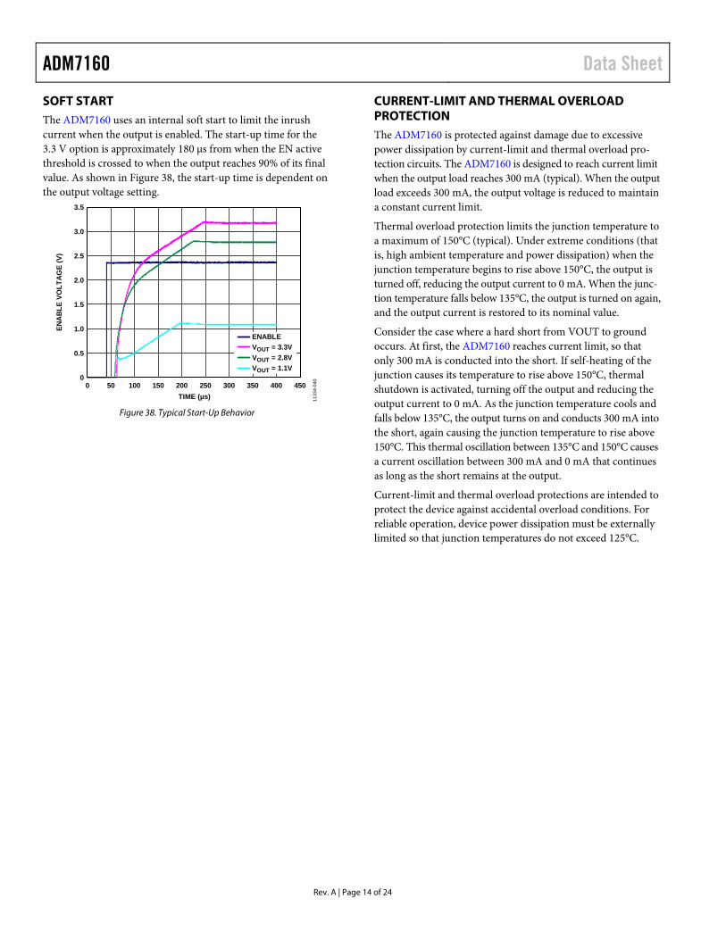
SOFT START The ADM7160 uses an internal soft start to limit the inrush current when the output is enabled. The start-up time for the 3.3 V option is approximately 180 μs from when the EN active threshold is crossed to when the output reaches 90% of its final value. As shown in Figure 38, the start-up time is dependent on the output voltage setting.
Figure 38. Typical Start-Up Behavior
CURRENT-LIMIT AND THERMAL OVERLOAD PROTECTION The ADM7160 is protected against damage due to excessive power dissipation by current-limit and thermal overload pro-tection circuits. The ADM7160 is designed to reach current limit when the output load reaches 300 mA (typical). When the output load exceeds 300 mA, the output voltage is reduced to maintain a constant current limit.
Thermal overload protection limits the junction temperature to a maximum of 150°C (typical). Under extreme conditions (that is, high ambient temperature and power dissipation) when the junction temperature begins to rise above 150°C, the output is turned off, reducing the output current to 0 mA. When the junc-tion temperature falls below 135°C, the output is turned on again, and the output current is restored to its nominal value.
Consider the case where a hard short from VOUT to ground occurs. At first, the ADM7160 reaches current limit, so that only 300 mA is conducted into the short. If self-heating of the junction causes its temperature to rise above 150°C, thermal shutdown is activated, turning off the output and reducing the output current to 0 mA. As the junction temperature cools and falls below 135°C, the output turns on and conducts 300 mA into the short, again causing the junction temperature to rise above 150°C. This thermal oscillation between 135°C and 150°C causes a current oscillation between 300 mA and 0 mA that continues as long as the short remains at the output.
Current-limit and thermal overload protections are intended to protect the device against accidental overload conditions. For reliable operation, device power dissipation must be externally limited so that junction temperatures do not exceed 125°C.
3.5
3.0
2.5
2.0
1.5
1.0
0.5
00 45040035030025020015010050
ENA
BLE
VO
LTA
GE
(V)
TIME (µs)
ENABLEVOUT = 3.3VVOUT = 2.8VVOUT = 1.1V
1133
4-04
0
Rev. A | Page 14 of 24

Data Sheet ADM7160
Rev. A | Page 15 of 24
APPLICATIONS INFORMATION CAPACITOR SELECTION Output Capacitor
The ADM7160 is designed for operation with small, space-saving ceramic capacitors, but it can function with most commonly used capacitors as long as care is taken with regard to the effective series resistance (ESR) value. The ESR of the output capacitor affects the stability of the LDO control loop. A minimum of 1 μF capacitance with an ESR of 1 Ω or less is recommended to ensure the stability of the ADM7160. Transient response to changes in load current is also affected by output capacitance. Using a larger value of output capacitance improves the transient response of the ADM7160 to large changes in load current. Figure 39 shows the transient response for an output capacitance value of 1 μF.
Figure 39. Output Transient Response, COUT = 1 μF
Input Bypass Capacitor
Connecting a 1 μF capacitor from VIN to GND reduces the circuit sensitivity to the PCB layout, especially when long input traces or high source impedance are encountered. If output capacitance greater than 1 μF is required, the input capacitor should be increased to match it.
Input and Output Capacitor Properties
Any good quality ceramic capacitor can be used with the ADM7160, as long as it meets the minimum capacitance and maximum ESR requirements. Ceramic capacitors are manufac-tured with a variety of dielectrics, each with different behavior over temperature and applied voltage. Capacitors must have an adequate dielectric to ensure the minimum capacitance over the required temperature range and dc bias conditions. X5R or X7R dielectrics with a voltage rating of 6.3 V or 10 V are recommended. Y5V and Z5U dielectrics are not recommended, due to their poor temperature and dc bias characteristics.
Figure 40 shows the capacitance vs. voltage bias characteristics of a 0402, 1 μF, 10 V, X5R capacitor. The voltage stability of a capacitor is strongly influenced by the capacitor size and voltage rating. In general, a capacitor in a larger package or with a higher voltage rating exhibits better stability. The temperature variation of the X5R dielectric is approximately ±15% over the −40°C to +85°C temperature range and is not a function of package or voltage rating.
Figure 40. Capacitance vs. Voltage Bias Characteristics
Use Equation 1 to determine the worst-case capacitance, accounting for capacitor variation over temperature, component tolerance, and voltage.
CEFF = CBIAS × (1 − TEMPCO) × (1 − TOL) (1)
where: CBIAS is the effective capacitance at the operating voltage. TEMPCO is the worst-case capacitor temperature coefficient. TOL is the worst-case component tolerance.
In this example, the worst-case temperature coefficient (TEMPCO) over −40°C to +85°C is assumed to be 15% for an X5R dielectric. The tolerance (TOL) of the capacitor is assumed to be 10%, and CBIAS is 0.94 μF at 1.8 V, as shown in Figure 40.
Substituting these values in Equation 1 yields
CEFF = 0.94 μF × (1 − 0.15) × (1 − 0.1) = 0.719 μF
Therefore, the capacitor selected in this example meets the minimum capacitance requirement of the LDO regulator over temperature and tolerance at the selected output voltage.
To guarantee the performance of the ADM7160, it is imperative that the effects of dc bias, temperature, and tolerance on the behavior of the capacitors be evaluated for each application.
CH1 200mA CH2 50mV M20µs A CH1 64mAT 10.00%
1
2
T
VOUT
1133
4-03
6
ILOAD
1.2
1.0
0.8
0.6
0.4
0.2
00 2 4 6 8 10
CA
PAC
ITA
NC
E (µ
F)
VOLTAGE BIAS (V) 1133
4-03
7

ADM7160 Data Sheet Figure 41 and Figure 42 show the connection of 4.7 μF capaci-tors on the VIN and VOUT pins for the 5-lead TSOT and 6-lead LFCSP packages, respectively.
Figure 41. 5-Lead TSOT with 4.7 μF Input and Output Capacitors
Figure 42. 6-Lead LFCSP with 4.7 μF Input and Output Capacitors
THERMAL CONSIDERATIONS In most applications, the ADM7160 does not dissipate much heat due to its high efficiency. However, in applications with high ambient temperature and a high supply voltage-to-output voltage differential, the heat dissipated in the package can cause the junction temperature of the die to exceed the maximum junction temperature of 125°C.
When the junction temperature exceeds 150°C, the ADM7160 enters thermal shutdown. To prevent any permanent damage, the regulator recovers only after the junction temperature decreases below 135°C. Therefore, thermal analysis for the selected applica-tion is very important to guarantee reliable performance over all conditions. The junction temperature of the die is the sum of the ambient temperature of the environment and the temperature rise of the package due to the power dissipation, as shown in Equation 2.
To guarantee reliable operation, the junction temperature of the ADM7160 must not exceed 125°C. To ensure that the junction temperature stays below this maximum value, the user must be aware of the parameters that contribute to junction temperature changes. These parameters include ambient temperature, power dissipation in the power device, and thermal resistance between the junction and ambient air (θJA). The θJA value is dependent on the package assembly compounds used and the amount of copper used to solder the package GND pin and the exposed pad (in the case of the LFCSP) to the PCB.
Table 6 shows typical θJA values for the 5-lead TSOT and 6-lead LFCSP packages for various PCB copper sizes.
Table 6. Typical θJA Values
Copper Size (mm2) θJA (°C/W)
TSOT LFCSP 01 170 231.2 50 152 161.8 100 146 150.1 300 134 111.5 500 131 91.8 1 Device soldered to minimum size pin traces.
Table 7 shows the typical ΨJB values for the 5-lead TSOT and 6-lead LFCSP.
Table 7. Typical ΨJB Values Package ΨJB (°C/W) TSOT 43 LFCSP 28.3
The junction temperature of the ADM7160 can be calculated using the following equation:
TJ = TA + (PD × θJA) (2)
where: TA is the ambient temperature. θJA is the junction-to-ambient thermal resistance of the package. PD is the power dissipation in the die, given by
PD = [(VIN − VOUT) × ILOAD] + (VIN × IGND) (3)
where: VIN and VOUT are the input and output voltages, respectively. ILOAD is the load current. IGND is the ground current.
Power dissipation due to ground current is quite small and can be ignored. Therefore, the junction temperature equation can be simplified as follows:
TJ = TA + {[(VIN − VOUT) × ILOAD] × θJA} (4)
As shown in Equation 4, for a given ambient temperature, input-to-output voltage differential, and continuous load current, a minimum copper size requirement exists for the PCB to ensure that the junction temperature does not exceed 125°C.
Figure 43 through Figure 54 show junction temperature calculations for various ambient temperatures, load currents, input-to-output voltage differentials, and areas of PCB copper.
1
2
3
5
4
CIN4.7µF
COUT4.7µF
VOUT = 2.5VVIN = 2.9VVOUT
NC
VIN
GND
ADM7160
ENOFF
ON
1133
4-00
1
NC = NO CONNECT. DO NOTCONNECT TO THIS PIN.
ADM7160TOP VIEW
(Not to Scale)4
6
5
GND
VOUT
NC
3
1
2
EN
VIN
NC
1133
4-10
2
NC = NO CONNECT. DO NOTCONNECT TO THIS PIN.
ONOFF
CIN4.7µF
COUT4.7µF
VIN = 2.9V VOUT = 2.5V
Rev. A | Page 16 of 24

Data Sheet ADM7160
Figure 43. TSOT, 500 mm2 of PCB Copper, TA = 25°C
Figure 44. TSOT, 100 mm2 of PCB Copper, TA = 25°C
Figure 45. TSOT, 50 mm2 of PCB Copper, TA = 25°C
Figure 46. TSOT, 500 mm2 of PCB Copper, TA = 50°C
Figure 47. TSOT, 100 mm2 of PCB Copper, TA = 50°C
Figure 48. TSOT, 50 mm2 of PCB Copper, TA = 50°C
140
120
100
80
60
40
20
00.3 4.84.33.83.32.82.31.81.30.8
VIN – VOUT (V)
JUN
CTI
ON
TEM
PER
ATU
RE,
TJ
(°C
)
ILOAD = 1mAILOAD = 10mAILOAD = 50mA
ILOAD = 100mAILOAD = 150mAILOAD = 200mA
MAXIMUM JUNCTION TEMPERATURE
1133
4-04
1
140
120
100
80
60
40
20
00.3 4.84.33.83.32.82.31.81.30.8
VIN – VOUT (V)
JUN
CTI
ON
TEM
PER
ATU
RE,
TJ
(°C
)
ILOAD = 1mAILOAD = 10mAILOAD = 50mA
ILOAD = 100mAILOAD = 150mAILOAD = 200mA
MAXIMUM JUNCTION TEMPERATURE
1133
4-04
2
140
120
100
80
60
40
20
00.3 4.84.33.83.32.82.31.81.30.8
VIN – VOUT (V)
JUN
CTI
ON
TEM
PER
ATU
RE,
TJ
(°C
)
ILOAD = 1mAILOAD = 10mAILOAD = 50mA
ILOAD = 100mAILOAD = 150mAILOAD = 200mA
MAXIMUM JUNCTION TEMPERATURE
1133
4-04
3
140
120
100
80
60
40
20
00.3 4.84.33.83.32.82.31.81.30.8
VIN – VOUT (V)
JUN
CTI
ON
TEM
PER
ATU
RE,
TJ
(°C
)
ILOAD = 1mAILOAD = 10mAILOAD = 50mA
ILOAD = 100mAILOAD = 150mAILOAD = 200mA
MAXIMUM JUNCTION TEMPERATURE
1133
4-04
4
140
120
100
80
60
40
20
00.3 4.84.33.83.32.82.31.81.30.8
VIN – VOUT (V)
JUN
CTI
ON
TEM
PER
ATU
RE,
TJ
(°C
)
ILOAD = 1mAILOAD = 10mAILOAD = 50mA
ILOAD = 100mAILOAD = 150mAILOAD = 200mA
MAXIMUM JUNCTION TEMPERATURE
1133
4-04
5
140
120
100
80
60
40
20
00.3 4.84.33.83.32.82.31.81.30.8
VIN – VOUT (V)
JUN
CTI
ON
TEM
PER
ATU
RE,
TJ
(°C
)
ILOAD = 1mAILOAD = 10mAILOAD = 50mA
ILOAD = 100mAILOAD = 150mAILOAD = 200mA
MAXIMUM JUNCTION TEMPERATURE
1133
4-04
6
Rev. A | Page 17 of 24

ADM7160 Data Sheet
Figure 49. LFCSP, 500 mm2 of PCB Copper, TA = 25°C
Figure 50. LFCSP, 100 mm2 of PCB Copper, TA = 25°C
Figure 51. LFCSP, 50 mm2 of PCB Copper, TA = 25°C
Figure 52. LFCSP, 500 mm2 of PCB Copper, TA = 50°C
Figure 53. LFCSP, 100 mm2 of PCB Copper, TA = 50°C
Figure 54. LFCSP, 50 mm2 of PCB Copper, TA = 50°C
140
120
100
80
60
40
20
00.3 4.84.33.83.32.82.31.81.30.8
VIN – VOUT (V)
JUN
CTI
ON
TEM
PER
ATU
RE,
TJ
(°C
)
ILOAD = 1mAILOAD = 10mAILOAD = 50mA
ILOAD = 100mAILOAD = 150mAILOAD = 200mA
MAXIMUM JUNCTION TEMPERATURE
1133
4-04
7
140
120
100
80
60
40
20
00.3 4.84.33.83.32.82.31.81.30.8
VIN – VOUT (V)
JUN
CTI
ON
TEM
PER
ATU
RE,
TJ
(°C
)
ILOAD = 1mAILOAD = 10mAILOAD = 50mA
ILOAD = 100mAILOAD = 150mAILOAD = 200mA
MAXIMUM JUNCTION TEMPERATURE
1133
4-04
8
140
120
100
80
60
40
20
00.3 4.84.33.83.32.82.31.81.30.8
VIN – VOUT (V)
JUN
CTI
ON
TEM
PER
ATU
RE,
TJ
(°C
)
ILOAD = 1mAILOAD = 10mAILOAD = 50mA
ILOAD = 100mAILOAD = 150mAILOAD = 200mA
MAXIMUM JUNCTION TEMPERATURE
1133
4-04
9
140
120
100
80
60
40
20
00.3 4.84.33.83.32.82.31.81.30.8
VIN – VOUT (V)
JUN
CTI
ON
TEM
PER
ATU
RE,
TJ
(°C
)
ILOAD = 1mAILOAD = 10mAILOAD = 50mA
ILOAD = 100mAILOAD = 150mAILOAD = 200mA
MAXIMUM JUNCTION TEMPERATURE
1133
4-05
0
140
120
100
80
60
40
20
00.3 4.84.33.83.32.82.31.81.30.8
VIN – VOUT (V)
JUN
CTI
ON
TEM
PER
ATU
RE,
TJ
(°C
)
ILOAD = 1mAILOAD = 10mAILOAD = 50mA
ILOAD = 100mAILOAD = 150mAILOAD = 200mA
MAXIMUM JUNCTION TEMPERATURE
1133
4-05
1
140
120
100
80
60
40
20
00.3 4.84.33.83.32.82.31.81.30.8
VIN – VOUT (V)
JUN
CTI
ON
TEM
PER
ATU
RE,
TJ
(°C
)
ILOAD = 1mAILOAD = 10mAILOAD = 50mA
ILOAD = 100mAILOAD = 150mAILOAD = 200mA
MAXIMUMJUNCTION
TEMPERATURE11
334-
052
Rev. A | Page 18 of 24

Data Sheet ADM7160 In cases where the board temperature is known, use the ΨJB thermal characterization parameter to estimate the junction temperature rise (see Figure 55 and Figure 56). Maximum junc-tion temperature (TJ) is calculated from the board temperature (TB) and the power dissipation (PD) using the following formula:
TJ = TB + (PD × ΨJB) (5)
The typical value of ΨJB is 43°C/W for the 5-lead TSOT package and 28.3°C/W for the 6-lead LFCSP package.
Figure 55. TSOT, TA = 85°C
Figure 56. LFCSP, TA = 85°C
PCB LAYOUT CONSIDERATIONS Heat dissipation from the package can be improved by increas-ing the amount of copper attached to the pins of the ADM7160. However, as shown in Table 6, a point of diminishing returns is eventually reached, beyond which an increase in the copper size does not yield significant heat dissipation benefits.
Place the input capacitor as close as possible to the VIN and GND pins. Place the output capacitor as close as possible to the VOUT and GND pins. Use of 0402 or 0603 size capacitors achieves the smallest possible footprint solution on boards where area is limited.
Figure 57. Example of PCB Layout, TSOT Package
Figure 58. Example of PCB Layout, LFCSP Package
140
120
100
80
60
40
20
00.3 4.84.33.83.32.82.31.81.30.8
VIN – VOUT (V)
JUN
CTI
ON
TEM
PER
ATU
RE,
TJ
(°C
)
ILOAD = 1mAILOAD = 10mAILOAD = 50mA
ILOAD = 100mAILOAD = 150mAILOAD = 200mA
MAXIMUM JUNCTION TEMPERATURE
1133
4-05
3
140
120
100
80
60
40
20
00.3 5.34.33.32.31.3
VIN – VOUT (V)
JUN
CTI
ON
TEM
PER
ATU
RE,
TJ
(°C
)
ILOAD = 1mAILOAD = 10mAILOAD = 50mA
ILOAD = 100mAILOAD = 150mAILOAD = 200mA
MAXIMUM JUNCTION TEMPERATURE
1133
4-05
4
1133
4-05
511
334-
056
Rev. A | Page 19 of 24

ADM7160 Data Sheet
TYPICAL APPLICATION CIRCUITS
Figure 59. ADM7160 Powering a 16-Bit/18-Bit ADC
Figure 60. ADM7160 Powering a PLL/VCO
1
2
3
5
4
16-BIT/18-BIT ADC
CIN4.7µF
COUT4.7µF
VOUT = 2.5VVIN = 2.9VVOUT
NC
VIN
GND
ADM7160
ENOFF
ON
1133
4-10
1
NC = NO CONNECT
VDD
VDD
IN+
IN–
VREFDVDD
DIGITALOUTPUT
1.8V TO 5V
2.5V TO 5V
0V TO VREF
1
2
3
5
4
CIN4.7µF
COUT4.7µF
VOUT = 3.3V
VCP VVCO
DVDD
VIN = 5VVOUT
INPUT OUTPUTNC
VIN
GND
ADM7160
ENOFF
ON
NC = NO CONNECT
1
2
3
5
4
CIN4.7µF
COUT4.7µF
VOUT = 3.3VVIN = 5VVOUT
NC
VIN
GND
ADM7160
ENOFF
ON
NC = NO CONNECT
N DIVIDER
PHASEDETECTOR
CHARGEPUMP
PLL BLOCK DIAGRAM
LOOPFILTER VCO
VOLTAGE-CONTROLLEDOSCILLATOR
AVDD
1133
4-00
2
Rev. A | Page 20 of 24

Data Sheet ADM7160
OUTLINE DIMENSIONS
Figure 61. 5-Lead Thin Small Outline Transistor Package [TSOT]
(UJ-5) Dimensions shown in millimeters
Figure 62. 6-Lead Lead Frame Chip Scale Package [LFCSP_UD]
2.00 mm × 2.00 mm Body, Ultra Thin, Dual Lead (CP-6-3)
Dimensions shown in millimeters
1007
08-A
*COMPLIANT TO JEDEC STANDARDS MO-193-AB WITHTHE EXCEPTION OF PACKAGE HEIGHT AND THICKNESS.
1.60 BSC 2.80 BSC
1.90BSC
0.95 BSC
0.200.08
0.600.450.30
8°4°0°
0.500.30
0.10 MAX
*1.00 MAX
*0.90 MAX0.70 MIN
2.90 BSC
5 4
1 2 3
SEATINGPLANE
1.701.601.50
0.4250.3500.275
TOP VIEW
6
1
4
3
0.350.300.25
BOTTOM VIEW
PIN 1 INDEXAREA
SEATINGPLANE
0.600.550.50
1.101.000.90
0.20 REF
0.05 MAX0.02 NOM
0.65 BSC
EXPOSEDPAD
PIN 1INDICATOR(R 0.15)
FOR PROPER CONNECTION OFTHE EXPOSED PAD, REFER TOTHE PIN CONFIGURATION ANDFUNCTION DESCRIPTIONSSECTION OF THIS DATA SHEET.
02-0
6-20
13-D
0.15 REF
2.102.00 SQ1.90
0.20 MIN
Rev. A | Page 21 of 24

ADM7160 Data Sheet
ORDERING GUIDE Model1, 2 Temperature Range Output Voltage (V) Package Description Package Option Branding ADM7160AUJZ-1.8-R7 −40°C to +125°C 1.8 5-Lead TSOT UJ-5 LNH ADM7160AUJZ-2.5-R7 −40°C to +125°C 2.5 5-Lead TSOT UJ-5 LNJ ADM7160AUJZ-3.3-R7 −40°C to +125°C 3.3 5-Lead TSOT UJ-5 LNK ADM7160AUJZ-1.8-R2 −40°C to +125°C 1.8 5-Lead TSOT UJ-5 LNH ADM7160AUJZ-2.5-R2 −40°C to +125°C 2.5 5-Lead TSOT UJ-5 LNJ ADM7160AUJZ-3.3-R2 −40°C to +125°C 3.3 5-Lead TSOT UJ-5 LNK ADM7160ACPZN1.8-R7 −40°C to +125°C 1.8 6-Lead LFCSP_UD CP-6-3 LNH ADM7160ACPZN2.5-R7 −40°C to +125°C 2.5 6-Lead LFCSP_UD CP-6-3 LNJ ADM7160ACPZN3.3-R7 −40°C to +125°C 3.3 6-Lead LFCSP_UD CP-6-3 LNK ADM7160ACPZN1.8-R2 −40°C to +125°C 1.8 6-Lead LFCSP_UD CP-6-3 LNH ADM7160ACPZN2.5-R2 −40°C to +125°C 2.5 6-Lead LFCSP_UD CP-6-3 LNJ ADM7160ACPZN3.3-R2 −40°C to +125°C 3.3 6-Lead LFCSP_UD CP-6-3 LNK ADM7160CP-EVALZ Evaluation Board for
LFCSP_UD
ADM7160UJ-EVALZ Evaluation Board for TSOT
1 Z = RoHS Compliant Part. 2 For additional voltage options, contact your local Analog Devices, Inc., sales or distribution representative.
Rev. A | Page 22 of 24

Data Sheet ADM7160
NOTES
Rev. A | Page 23 of 24

ADM7160 Data Sheet
NOTES
©2013–2014 Analog Devices, Inc. All rights reserved. Trademarks and registered trademarks are the property of their respective owners. D11334-0-4/14(A)
Rev. A | Page 24 of 24