Embed Size (px)
Citation preview

TPS799xx
GNDEN NR
IN OUTVIN VOUT
Optional input capacitor.
May improve source
impedance, noise, or PSRR.
Optional bypass capacitor
to reduce output noise
and increase PSRR.
2.2mF
Ceramic
VEN
TPS79901
GNDEN FB
IN OUTVIN VOUT
R1 CFB
R2
Optional input capacitor.
May improve source
impedance, noise, or PSRR.
V =OUT ´ 1.193(R1 2+ R )
R2
VEN
2.2 Fm
Ceramic
Product
Folder
Sample &Buy
Technical
Documents
Tools &
Software
Support &Community
TPS799SBVS056K –JANUARY 2005–REVISED JANUARY 2015
TPS799 200-mA, Low-Quiescent Current, Ultralow Noise, High-PSRR Low-Dropout LinearRegulator
1 Features 3 DescriptionThe TPS799 family of low-dropout (LDO), low-power
1• 200-mA Low-Dropout Regulator With ENlinear regulators offers excellent ac performance with• Multiple Output Voltage Versions Available: very low ground current. High power-supply rejection
– Fixed Outputs of 1.2 V to 4.5 V Using ratio (PSRR), low noise, fast start-up, and excellentInnovative Factory EEPROM Programming line and load transient response are provided while
consuming a very low 40-μA (typical) ground current.– Adjustable Outputs from 1.20 V to 6.5 VThe TPS799 is stable with ceramic capacitors and• Inrush Current Protection with EN Toggleuses an advanced BiCMOS fabrication process to• Low IQ: 40 μAyield a dropout voltage of typically 100 mV at a
• High PSRR: 66 dB at 1 kHz 200-mA output. The TPS799 uses a precision voltage• Stable with a Low-ESR, 2-μF Typical Output reference and feedback loop to achieve an overall
Capacitance accuracy of 2% over all load, line, process, andtemperature variations. The TPS799 features inrush• Excellent Load and Line Transient Responsecurrent protection when the EN toggle is used to start• 2% Overall Accuracy (Load, Line, and the device, immediately clamping the current.
Temperature)All devices are fully specified over the temperature• Very Low Dropout: 100 mV range of TJ = –40°C to 125°C, and offered in a low-
• Package: 5-Bump, Thin, 1-mm × 1.37-mm profile, die-sized ball grid array (DSBGA) package,DSBGA ideal for wireless handsets and WLAN cards.
2 Applications Device Information(1)
PART NUMBER PACKAGE BODY SIZE (NOM)• Cellular PhonesSOT (5) 2.90 mm x 1.60 mm• Wireless LAN, Bluetooth®
TPS799 SON (6) 2.00 x 2.00 mm• VCOs, RFDSBGA (5) 1.57 mm x 1.20 mm• Handheld Organizers, PDAs
(1) For all available packages, see the orderable addendum atthe end of the data sheet.
Typical Application Circuit Typical Application CircuitFixed Voltage Versions Adjustable Voltage Version
1
An IMPORTANT NOTICE at the end of this data sheet addresses availability, warranty, changes, use in safety-critical applications,intellectual property matters and other important disclaimers. PRODUCTION DATA.

TPS799SBVS056K –JANUARY 2005–REVISED JANUARY 2015 www.ti.com
Table of Contents7.4 Device Functional Modes........................................ 131 Features .................................................................. 1
8 Application and Implementation ........................ 142 Applications ........................................................... 18.1 Application Information............................................ 143 Description ............................................................. 18.2 Typical Applications ................................................ 144 Revision History..................................................... 28.3 Do's and Don'ts ...................................................... 165 Pin Configuration and Functions ......................... 3
9 Power Supply Recommendations ...................... 165.1 Fixed Voltage Versions ............................................. 310 Layout................................................................... 165.2 Adjustable Voltage Versions ..................................... 3
10.1 Layout Guidelines ................................................. 166 Specifications......................................................... 510.2 Layout Example .................................................... 176.1 Absolute Maximum Ratings ...................................... 510.3 Thermal Information .............................................. 176.2 ESD Ratings ............................................................ 5
11 Device and Documentation Support ................. 186.3 Recommended Operating Conditions....................... 511.1 Device Support...................................................... 186.4 Thermal Information .................................................. 511.2 Documentation Support ........................................ 186.5 Electrical Characteristics........................................... 611.3 Trademarks ........................................................... 186.6 Typical Characteristics .............................................. 711.4 Electrostatic Discharge Caution............................ 187 Detailed Description ............................................ 1211.5 Glossary ................................................................ 187.1 Overview ................................................................. 12
12 Mechanical, Packaging, and Orderable7.2 Functional Block Diagram ....................................... 12Information ........................................................... 187.3 Feature Description................................................. 13
4 Revision HistoryNOTE: Page numbers for previous revisions may differ from page numbers in the current version.
Changes from Revision J (August 2010) to Revision K Page
• Added ESD Ratings table, Feature Description section, Device Functional Modes, Application and Implementationsection, Power Supply Recommendations section, Layout section, Device and Documentation Support section, andMechanical, Packaging, and Orderable Information section ................................................................................................. 1
• Changed Features list ........................................................................................................................................................... 1• Changed Description section.................................................................................................................................................. 1• Changed figure on front page; replaced device pinouts with application circuits................................................................... 1• Changed Pin Configuration and Functions section; updated table format, renamed pin packages to meet new
standards ............................................................................................................................................................................... 3• Changed "free-air" to "junction" temperature in condition statement for Absolute Maximum Ratings .................................. 5• Changed free-air to junction in Recommended Operating Conditions table conditions......................................................... 5• Added thermal information for additional device packages ................................................................................................... 5
Changes from Revision I (November 2007) to Revision J Page
• Replaced the Dissipation Ratings table with the Thermal Information table .......................................................................... 5
2 Submit Documentation Feedback Copyright © 2005–2015, Texas Instruments Incorporated
Product Folder Links: TPS799
6
5
4
1
2
3
GND
OUT
FB
IN
GND EN
N/C
OUT
FB
IN
GND
EN
C3 C1
B2
A3 A1
1
2
3
5
4
OUT
FB
IN
GND
EN
6
5
4
1
2
3
GND
OUT
NR
IN
GND EN
N/C
OUT
NR
IN
GND
EN
C3 C1
B2
A3 A1
1
2
3
5
4
OUT
NR
IN
GND
EN
TPS799www.ti.com SBVS056K –JANUARY 2005–REVISED JANUARY 2015
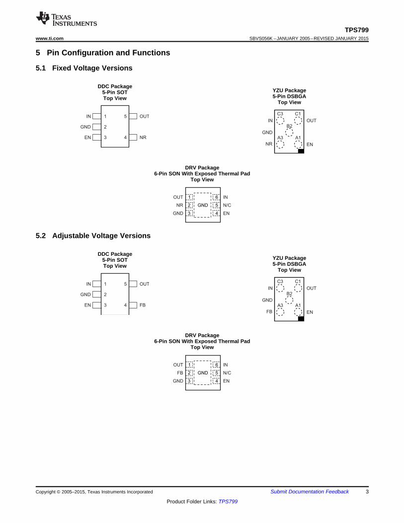
5 Pin Configuration and Functions
5.1 Fixed Voltage Versions
DDC PackageYZU Package5-Pin SOT5-Pin DSBGATop View
Top View
DRV Package6-Pin SON With Exposed Thermal Pad
Top View
5.2 Adjustable Voltage Versions
DDC PackageYZU Package5-Pin SOT5-Pin DSBGATop View
Top View
DRV Package6-Pin SON With Exposed Thermal Pad
Top View
Copyright © 2005–2015, Texas Instruments Incorporated Submit Documentation Feedback 3
Product Folder Links: TPS799

TPS799SBVS056K –JANUARY 2005–REVISED JANUARY 2015 www.ti.com
Pin FunctionsPIN
I/O DESCRIPTIONNAME DDC YZY DRV
IN 1 C3 6 I Input supply.GND 2 B2 3, Pad — Ground. The pad must be tied to GND.
Driving this pin high turns on the regulator. Driving this pin low puts the regulator intoEN 3 A1 4 I shutdown mode. EN can be connected to IN if not used.Fixed voltage versions only. Noise reduction; connecting this pin to an external capacitor
NR 4 A3 2 — bypasses noise generated by the internal band gap. This capacitor allows output noise tobe reduced to very low levels.Adjustable voltage version only. Feedback; this pin is the input to the control loop errorFB 4 A3 2 I amplifier, and sets the output voltage of the device.Output of the regulator. To assure stability, a small ceramic capacitor (total typicalOUT 5 C1 1 O capacitance ≥ 2 μF) is required from this pin to ground.
N/C — — 5 — Not internally connected. This pin must either be left open, or tied to GND.
4 Submit Documentation Feedback Copyright © 2005–2015, Texas Instruments Incorporated
Product Folder Links: TPS799
TPS799www.ti.com SBVS056K –JANUARY 2005–REVISED JANUARY 2015
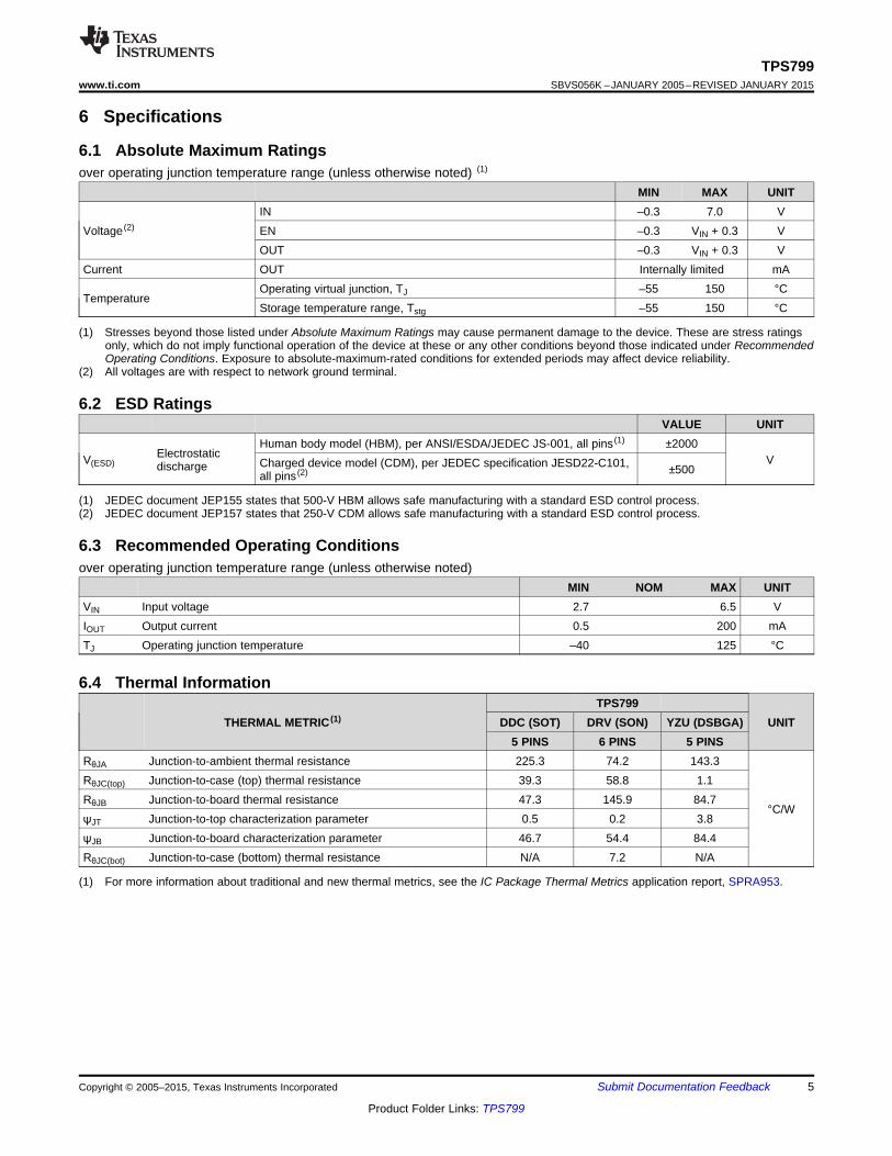
6 Specifications
6.1 Absolute Maximum Ratingsover operating junction temperature range (unless otherwise noted) (1)
MIN MAX UNITIN –0.3 7.0 V
Voltage (2) EN –0.3 VIN + 0.3 VOUT –0.3 VIN + 0.3 V
Current OUT Internally limited mAOperating virtual junction, TJ –55 150 °C
TemperatureStorage temperature range, Tstg –55 150 °C
(1) Stresses beyond those listed under Absolute Maximum Ratings may cause permanent damage to the device. These are stress ratingsonly, which do not imply functional operation of the device at these or any other conditions beyond those indicated under RecommendedOperating Conditions. Exposure to absolute-maximum-rated conditions for extended periods may affect device reliability.
(2) All voltages are with respect to network ground terminal.
6.2 ESD RatingsVALUE UNIT
Human body model (HBM), per ANSI/ESDA/JEDEC JS-001, all pins (1) ±2000ElectrostaticV(ESD) VCharged device model (CDM), per JEDEC specification JESD22-C101,discharge ±500all pins (2)
(1) JEDEC document JEP155 states that 500-V HBM allows safe manufacturing with a standard ESD control process.(2) JEDEC document JEP157 states that 250-V CDM allows safe manufacturing with a standard ESD control process.
6.3 Recommended Operating Conditionsover operating junction temperature range (unless otherwise noted)
MIN NOM MAX UNITVIN Input voltage 2.7 6.5 VIOUT Output current 0.5 200 mATJ Operating junction temperature –40 125 °C
6.4 Thermal InformationTPS799
THERMAL METRIC (1) DDC (SOT) DRV (SON) YZU (DSBGA) UNIT5 PINS 6 PINS 5 PINS
RθJA Junction-to-ambient thermal resistance 225.3 74.2 143.3RθJC(top) Junction-to-case (top) thermal resistance 39.3 58.8 1.1RθJB Junction-to-board thermal resistance 47.3 145.9 84.7
°C/WψJT Junction-to-top characterization parameter 0.5 0.2 3.8ψJB Junction-to-board characterization parameter 46.7 54.4 84.4RθJC(bot) Junction-to-case (bottom) thermal resistance N/A 7.2 N/A
(1) For more information about traditional and new thermal metrics, see the IC Package Thermal Metrics application report, SPRA953.
Copyright © 2005–2015, Texas Instruments Incorporated Submit Documentation Feedback 5
Product Folder Links: TPS799

TPS799SBVS056K –JANUARY 2005–REVISED JANUARY 2015 www.ti.com
6.5 Electrical CharacteristicsOver operating temperature range (TJ = –40°C to 125°C), VIN = VOUT(nom) + 0.3 V or 2.7 V, whichever is greater; IOUT = 1 mA,VEN = VIN, COUT = 2.2 μF, CNR = 0.01 μF, unless otherwise noted. For TPS79901, VOUT = 3.0 V. Typical values are at TJ =25°C.
PARAMETER TEST CONDITIONS MIN TYP MAX UNITVIN Input voltage range (1) 2.7 6.5 VVFB Internal reference (TPS79901) 1.169 1.193 1.217 VVOUT Output voltage range (TPS79901) VFB 6.5 – VDO V
Output accuracy, nominal TJ = 25°C –1% 1%VOUT Output accuracy (1) VOUT + 0.3 V ≤ VIN ≤ 6.5 V –2% ±1% 2%Over VIN, IOUT, temperature 500 μA ≤ IOUT ≤ 200 mAΔVO(ΔVI) Line regulation (1) VOUT(NOM) + 0.3 V ≤ VIN ≤ 6.5 V 0.02 %/VΔVO(ΔIO) Load regulation 500 μA ≤ IOUT ≤ 200 mA 0.002 %/mA
VOUT(nom) ≤ 3.3 V 100 175 mVDropout voltage (2)VDO IOUT = 200 mA(VIN = VOUT(nom) – 0.1 V) VOUT(nom) ≥ 3.3 V 90 160 mVICL Output current limit VOUT = 0.9 × VOUT(nom) 220 400 600 mAIGND Ground pin current 500 μA ≤ IOUT ≤ 200 mA 40 60 μAISHDN Shutdown current (IGND) VEN ≤ 0.4 V, 2.7 V ≤ VIN ≤ 6.5 V 0.15 1 μAIFB Feedback pin current (TPS79901) –0.5 0.5 µA
f = 100 Hz 70 dBVIN = 3.85 V,
f = 1 kHz 66 dBVOUT = 2.85 V,PSRR Power-supply rejection ratio CNR = 0.01 μF, f = 10 kHz 51 dBIOUT = 100 mA
f = 100 kHz 38 dBCNR = 0.01 μF 10.5 × VOUT μVRMSBW = 10 Hz to 100 kHz,Vn Output noise voltage VOUT = 2.85 V CNR = none 94 × VOUT μVRMS
CNR = 0.001 μF 45 μsVOUT = 2.85 V, CNR = 0.047 μF 45 μs
Start-up time RL = 14 Ω,CNR = 0.01 μF 50 μsCOUT = 2.2 μFCNR = none 50 μs
VEN(HI) Enable high (enabled) 1.2 VIN VVEN(LO) Enable low (shutdown) 0 0.4 VIEN(HI) Enable pin current, enabled VEN = VIN = 6.5 V 0.03 1 μA
Shutdown, temperature increasing 165 °CTsd Thermal shutdown temperature
Reset, temperature decreasing 145 °CTJ Operating junction temperature –40 125 °C
Undervoltage lockout VIN rising 1.90 2.20 2.65 VUVLO
Hysteresis VIN falling 70 mV
(1) Minimum VIN = VOUT + VDO or 2.7 V, whichever is greater.(2) VDO is not measured for devices with VOUT(nom) < 2.8 V because minimum VIN = 2.7 V.
6 Submit Documentation Feedback Copyright © 2005–2015, Texas Instruments Incorporated
Product Folder Links: TPS799

TJ (°C)
200
180
160
140
120
100
80
60
40
20
0
VD
O(m
V)
5 35 65 9550 12520 80 110
IOUT = 100mA
IOUT = 200mA
IOUT = 1mA
−40 −25 −15
110
100
90
80
70
60
50
40
30
20
10
0
VD
O(m
V)
2.5 3.0 3.5 4.0 5.0 6.0 7.04.5 5.5 6.5
VIN (V)
IOUT = 200mA
TJ (°C)
2.0
1.5
1.0
0.5
0
−0.5
−1.0
−1.5
−2.0
Cha
nge
inV
OU
T(%
)
IOUT = 100mA
IOUT = 200mA
IOUT = 1mA
−40 −25 5 35 65 9550 125−15 20 80 110
200
180
160
140
120
100
80
60
40
20
0
VD
O(m
V)
0 50 100 150 200
IOUT (mA)
TJ = +85C
TJ = −40C
TJ = +125C
TJ = +25C
0 50 100 150 200
IOUT (mA)
28.50
21.38
14.25
7.13
0
−7.13
−14.25
−21.38
−28.50
Cha
nge
inV
OU
T(m
V)
TJ = +125°C TJ = +85°C
TJ = −40°C
TJ = +25°C
2.5 3.5 4.5 5.5 6.5
VIN (V)
1.0
0.8
0.6
0.4
0.2
0
−0.2
−0.4
−0.6
−0.8
−1.0
Cha
nge
inV
OU
T(%
)
7.5
IOUT = 100mA
TJ = +125°C
TJ = +85°C
TJ = −40°C
TJ = +25°C
TPS799www.ti.com SBVS056K –JANUARY 2005–REVISED JANUARY 2015
6.6 Typical CharacteristicsOver operating temperature range (TJ= –40°C to 125°C), VIN = VOUT(nom) + 0.3 V or 2.7 V, whichever is greater; IOUT = 1 mA,VEN = VIN, COUT = 2.2 μF, and CNR = 0.01 μF, unless otherwise noted. For TPS79901, VOUT = 3.0 V. Typical values are at TJ= 25°C.
Figure 2. Line RegulationFigure 1. Load Regulation
Figure 4. TPS799285 Dropout Voltage vs Output CurrentFigure 3. Output Voltage vs Junction Temperature
Figure 6. TPS79901 Dropout vs Input VoltageFigure 5. TPS799285 Dropout Voltage vs JunctionTemperature
Copyright © 2005–2015, Texas Instruments Incorporated Submit Documentation Feedback 7
Product Folder Links: TPS799

90
80
70
60
50
40
30
20
10
010 100 1k 10k
Frequency (Hz)
PS
RR
(dB
)
100k 1M 10M
IOUT = 100mA IOUT = 1mA
IOUT = 200mACNR = 0.01µFCOUT = 2.2µF
90
80
70
60
50
40
30
20
10
010 100 1k 10k
Frequency (Hz)
PS
RR
(dB
)
100k 1M 10M
IOUT = 1mA
IOUT = 100mA
IOUT = 200mA
CNR = 0.01µFCOUT = 2.2µF
TJ (°C)
600
500
400
300
200
100
0
I GN
D(n
A)
VEN = 0.4V
VIN = 6.5V
VIN = 3.2V
−40 −25 5 35 65 9550 125−15 20 80 110
90
80
70
60
50
40
30
20
10
010 100 1k 10k
Frequency (Hz)
PS
RR
(dB
)
100k 1M 10M
IOUT = 200mA
IOUT = 100mA
IOUT = 1mA
CNR = 0.01µFCOUT = 2.2µF
60
50
40
30
20
10
0
I GN
D(µ
A)
VIN = 5.0V
VIN = 3.2V
VIN = 2.7V(dropout)
VOUT = 2.85VIOUT = 200mA
−40 −25 5 35 65 9550 125−15 20 80 110
TJ (°C)
60
50
40
30
20
10
0
I(
A)
GN
Dm
2.5 3.0 4.5 5.5 6.5
V (V)IN
7.03.5 4.0 5.0 6.0
I = 200mAOUT
V = 2.85VOUT
I = 500 AOUT m
TPS799SBVS056K –JANUARY 2005–REVISED JANUARY 2015 www.ti.com
Typical Characteristics (continued)Over operating temperature range (TJ= –40°C to 125°C), VIN = VOUT(nom) + 0.3 V or 2.7 V, whichever is greater; IOUT = 1 mA,VEN = VIN, COUT = 2.2 μF, and CNR = 0.01 μF, unless otherwise noted. For TPS79901, VOUT = 3.0 V. Typical values are at TJ= 25°C.
Figure 7. Ground Pin Current vs Input Voltage Figure 8. TPS799285 Ground Pin Current vs JunctionTemperature
Figure 10. TPS799285 Power-Supply Ripple Rejection vsFigure 9. Ground Pin Current (Disabled) vs JunctionFrequency (VIN – VOUT = 1.0 V)Temperature
Figure 11. TPS799285 Power-Supply Ripple Rejection vs Figure 12. TPS799285 Power-Supply Ripple Rejection vsFrequency (VIN – VOUT = 0.5 V) Frequency (VIN – VOUT = 0.25 V)
8 Submit Documentation Feedback Copyright © 2005–2015, Texas Instruments Incorporated
Product Folder Links: TPS799

90
80
70
60
50
40
30
20
10
00.0 1.0 1.50.5 2.0 2.5
VIN − VOUT (V)
PS
RR
(dB
)
3.0 3.5 4.0
0.1kHz1kHz
10kHz
100kHz 1MHz
CNR = 0.01µFCOUT = 2.2µF
90
80
70
60
50
40
30
20
10
00.0 1.0 1.50.5 2.0 2.5
VIN − VOUT (V)
PS
RR
(dB
)
3.0 3.5 4.0
0.1kHz
100kHz
1kHz
10kHz
1MHz
CNR = 0.01µFCOUT = 2.2µF
90
80
70
60
50
40
30
20
10
0
PS
RR
(dB
)
0.0 1.0 1.50.5 2.0 2.5
VIN − VOUT (V)
3.0 3.5 4.0
0.1kHz
10kHz
1kHz
100kHz
1MHz
CNR = 0.01µFCOUT = 2.2µF
90
80
70
60
50
40
30
20
10
010 100 1k 10k
Frequency (Hz)
PS
RR
(dB
)
100k 1M 10M
IOUT = 200mACNR = NoneCOUT = 10.0µF
IOUT = 1mA
90
80
70
60
50
40
30
20
10
010 100 1k 10k
Frequency (Hz)
PS
RR
(dB
)
100k 1M 10M
IOUT = 1mA
IOUT = 200mA
CNR = 0.01µFCOUT = 10.0µF
90
80
70
60
50
40
30
20
10
010 100 1k 10k
Frequency (Hz)
PS
RR
(dB
)
100k 1M 10M
IOUT = 1mA
IOUT = 200mA
CNR = 0.01µFCOUT = 10.0µF
TPS799www.ti.com SBVS056K –JANUARY 2005–REVISED JANUARY 2015
Typical Characteristics (continued)Over operating temperature range (TJ= –40°C to 125°C), VIN = VOUT(nom) + 0.3 V or 2.7 V, whichever is greater; IOUT = 1 mA,VEN = VIN, COUT = 2.2 μF, and CNR = 0.01 μF, unless otherwise noted. For TPS79901, VOUT = 3.0 V. Typical values are at TJ= 25°C.
Figure 13. TPS799285 Power-Supply Ripple Rejection vs Figure 14. TPS799285 Power-Supply Ripple Rejection vsFrequency (VIN – VOUT = 1.0 V) Frequency (VIN – VOUT = 0.25 V)
Figure 15. TPS799285 Power-Supply Ripple Rejection vs Figure 16. Power-Supply Ripple Rejection vs VIN – VOUT, IOUTFrequency (VIN – VOUT = 1.0 V) = 1 mA
Figure 17. Power-Supply Ripple Rejection vs VIN – VOUT, IOUT Figure 18. Power-Supply Ripple Rejection vs VIN – VOUT, IOUT= 100 mA = 200 mA
Copyright © 2005–2015, Texas Instruments Incorporated Submit Documentation Feedback 9
Product Folder Links: TPS799

10 s/divm
1V/div
4V/div
VOUT
VIN0V
3.85V
R WLOAD = 19
C = 10 FOUT m
R WLOAD = 19
C = 2.2 FOUT m
10 s/divm
1V/div
5V/div
VOUT
VEN
R WLOAD = 19
C = 2.2 FOUT mR WLOAD = 19
C = 10 FOUT m
V = 3.85VIN
20 s/divm
100mV/div
100mV/div
100mA/div
VOUT
VOUT
IOUT
C = 2.2 FOUT m
C = 10 FOUT m
V = 3.35VIN
150mA
1mA
20µs/div
20mV/div
20mV/div
1V/div
VOUT
VOUT
VIN
IOUT = 150mA
dVIN
dt= 1V/µs
COUT = 10µF
COUT = 2.2µF
3.15V
4.15V
200
180
160
140
120
100
80
60
40
20
00.01 0.1 1
CNR (nF)
10
IOUT = 1mACOUT = 2.2µF
Tota
lNoi
se(µ
Vrm
s)
35
30
25
20
15
10
5
00 5 10 15 20
COUT (µF)
Tota
lNoi
se(µ
Vrm
s)
25
IOUT = 1mACNR = 0.01µF
TPS799SBVS056K –JANUARY 2005–REVISED JANUARY 2015 www.ti.com
Typical Characteristics (continued)Over operating temperature range (TJ= –40°C to 125°C), VIN = VOUT(nom) + 0.3 V or 2.7 V, whichever is greater; IOUT = 1 mA,VEN = VIN, COUT = 2.2 μF, and CNR = 0.01 μF, unless otherwise noted. For TPS79901, VOUT = 3.0 V. Typical values are at TJ= 25°C.
Figure 19. TPS799285 Total Noise vs CNR Figure 20. TPS799285 Total Noise vs COUT
Figure 21. TPS799285 Line Transient Response Figure 22. TPS799285 Load Transient Response
Figure 23. TPS799285 Turn-On Response (VEN = VIN) Figure 24. TPS799285 Enable Response
10 Submit Documentation Feedback Copyright © 2005–2015, Texas Instruments Incorporated
Product Folder Links: TPS799

50ms/div
Vo
lts
7
6
5
4
3
2
1
0
−1
VIN
VOUT
RL = 19Ω
TPS799www.ti.com SBVS056K –JANUARY 2005–REVISED JANUARY 2015
Typical Characteristics (continued)Over operating temperature range (TJ= –40°C to 125°C), VIN = VOUT(nom) + 0.3 V or 2.7 V, whichever is greater; IOUT = 1 mA,VEN = VIN, COUT = 2.2 μF, and CNR = 0.01 μF, unless otherwise noted. For TPS79901, VOUT = 3.0 V. Typical values are at TJ= 25°C.
Figure 25. TPS799285 Power-Up/Power-Down
Copyright © 2005–2015, Texas Instruments Incorporated Submit Documentation Feedback 11
Product Folder Links: TPS799

ThermalShutdown
UVLO
CurrentLimit
2µA
OvershootDetect
500k
Quickstart
1.193VBandgap
IN
EN
NR
OUT
GND
400Ω
TPS799SBVS056K –JANUARY 2005–REVISED JANUARY 2015 www.ti.com
7 Detailed Description
7.1 OverviewThe TPS799 family of low-dropout (LDO) regulators combines the high performance required of many RF andprecision analog applications with ultralow current consumption. High PSRR is provided by a high-gain, high-bandwidth error loop with good supply rejection at very low headroom (VIN – VOUT). A noise-reduction pin isprovided to bypass noise generated by the band-gap reference and to improve PSRR, while a quick-start circuitquickly charges this capacitor at start-up. The combination of high performance and low ground current alsomake these devices an excellent choice for portable applications. All versions have thermal and overcurrentprotection, and are fully specified from –40°C to 125°C.
The TPS799 family also features inrush current protection with an EN toggle start-up, and overshoot detection atthe output. When the EN toggle is used to start the device, current limit protection is immediately activated,restricting the inrush current to the device. If voltage at the output overshoots 5% from the nominal value, apulldown resistor reduces the voltage to normal operating conditions, as shown in the Functional Block Diagram.
7.2 Functional Block Diagram
Figure 26. Fixed-Voltage Versions
12 Submit Documentation Feedback Copyright © 2005–2015, Texas Instruments Incorporated
Product Folder Links: TPS799

ThermalShutdown
UVLO
CurrentLimit
3.3MΩ
OvershootDetect
500k
1.193VBandgap
IN
EN
FB
OUT
GND
400Ω
TPS799www.ti.com SBVS056K –JANUARY 2005–REVISED JANUARY 2015
Functional Block Diagram (continued)
Figure 27. Adjustable-Voltage Versions
7.3 Feature Description
7.3.1 Internal Current LimitThe TPS799 internal current limit helps protect the regulator during fault conditions. In current limit mode, theoutput sources a fixed amount of current that is largely independent of the output voltage. For reliable operation,do not operate the device in a current-limit state for extended periods of time.
The PMOS pass element in the TPS799 has a built-in body diode that conducts current when the voltage at OUTexceeds the voltage at IN. This current is not limited; therefore, if extended reverse voltage operation isanticipated, external limiting may be required.
7.3.2 ShutdownThe enable pin (EN) is active high and is compatible with standard and low-voltage TTL-CMOS levels. Whenshutdown capability is not required, EN can be connected to IN.
7.3.3 Start UpThe TPS799 uses a start-up circuit to quickly charge the noise reduction capacitor, CNR, if present (see theFunctional Block Diagram). This circuit allows for the combination of very low output noise and fast start-uptimes. The NR pin is high impedance so a low leakage CNR capacitor must be used; most ceramic capacitors areappropriate for this configuration.
Note that for fastest start-up, apply VIN first, and then drive the enable pin (EN) high. If EN is tied to IN, start-up issomewhat slower. The start-up switch is closed for approximately 135 μs. To ensure that CNR is fully chargedduring start-up, use a 0.01-μF or smaller capacitor.
7.3.4 Undervoltage Lockout (UVLO)The TPS799 uses an undervoltage lockout circuit to keep the output shut off until internal circuitry is operatingproperly. The UVLO circuit has a deglitch feature so that undershoot transients are typically ignored on the inputif these transients are less than 50 μs in duration.
7.4 Device Functional ModesDriving EN over 1.2 V turns on the regulator. Driving EN below 0.4 V puts the regulator into shutdown mode,thus reducing the operating current to 150 nA, nominal.
Copyright © 2005–2015, Texas Instruments Incorporated Submit Documentation Feedback 13
Product Folder Links: TPS799

TPS79901
GNDEN FB
IN OUTVIN VOUT
R1 CFB
R2
Optional input capacitor.
May improve source
impedance, noise, or PSRR.
V =OUT ´ 1.193(R1 2+ R )
R2
VEN
2.2 Fm
Ceramic
TPS799xx
GNDEN NR
IN OUTVIN VOUT
Optional input capacitor.
May improve source
impedance, noise, or PSRR.
Optional bypass capacitor
to reduce output noise
and increase PSRR.
2.2mF
Ceramic
VEN
TPS799SBVS056K –JANUARY 2005–REVISED JANUARY 2015 www.ti.com
8 Application and Implementation
NOTEInformation in the following applications sections is not part of the TI componentspecification, and TI does not warrant its accuracy or completeness. TI’s customers areresponsible for determining suitability of components for their purposes. Customers shouldvalidate and test their design implementation to confirm system functionality.
8.1 Application InformationThe TPS799 family of LDO regulators provides high PSRR while maintaining ultralow current consumption. Thefamily also features inrush current protection and overshoot detection at the output.
8.2 Typical ApplicationsFigure 28 and Figure 29 show the basic circuit connections.
Figure 28. Typical Application Circuit for Fixed Voltage Versions
Figure 29. Typical Application Circuit for Adjustable Voltage Version
8.2.1 Design RequirementsSelect the desired device based on the output voltage.
Provide an input supply with adequate headroom to account for dropout and output current to account for theGND terminal current, and power the load.
8.2.2 Detailed Design Procedure
8.2.2.1 Input and Output Capacitor RequirementsAlthough an input capacitor is not required for stability, good analog design practice is to connect a 0.1-μF to1-μF low ESR capacitor across the input supply near the regulator. This capacitor counteracts reactive inputsources and improves transient response, noise rejection, and ripple rejection. A higher-value capacitor may benecessary if large, fast rise-time load transients are anticipated, or if the device is located several inches from thepower source. If source impedance is not sufficiently low, a 0.1-μF input capacitor may be necessary to ensurestability.
14 Submit Documentation Feedback Copyright © 2005–2015, Texas Instruments Incorporated
Product Folder Links: TPS799

V = x VN OUT
10.5 VmRMS
V
TPS799www.ti.com SBVS056K –JANUARY 2005–REVISED JANUARY 2015
Typical Applications (continued)The TPS799 is designed to be stable with standard ceramic capacitors with values of 2.2 μF or greater. X5R-and X7R-type capacitors are best because they have minimal variation in value and ESR over temperature.Maximum ESR must be less than 1.0 Ω.
8.2.2.2 Output NoiseIn most LDOs, the band gap is the dominant noise source. If a noise-reduction capacitor (CNR) is used with theTPS799, the band gap does not contribute significantly to noise. Instead, noise is dominated by the outputresistor divider and the error amplifier input. To minimize noise in a given application, use a 0.01-μF noisereduction capacitor. To further optimize noise, equivalent series resistance of the output capacitor can be set toapproximately 0.2 Ω. This configuration maximizes phase margin in the control loop, reducing total output noiseby up to 10%.
Noise can be referred to the feedback point; with CNR = 0.01 μF total noise is approximately given by Equation 1:
(1)
8.2.2.3 Dropout VoltageThe TPS799 uses a PMOS pass transistor to achieve a low dropout voltage. When (VIN – VOUT) is less than thedropout voltage (VDO), the PMOS pass device is in its linear region of operation and rDS(on) of the PMOS passelement is the input-to-output resistance. Because the PMOS device behaves like a resistor in dropout, VDOapproximately scales with the output current.
As with any linear regulator, PSRR degrades as (VIN – VOUT) approaches dropout. This effect is illustrated inFigure 10 through Figure 18 in the Typical Characteristics section.
8.2.2.4 Transient ResponseAs with any regulator, increasing the size of the output capacitor reduces over- and undershoot magnitude, butincreases the duration of the transient response. The transient response of the TPS799 is enhanced by an activepulldown device that engages when the output overshoots by approximately 5% or more when the device isenabled. When enabled, the pulldown device behaves like a 350-Ω resistor to ground.
8.2.2.5 Minimum LoadThe TPS799 is stable with no output load. To meet the specified accuracy, a minimum load of 500 μA isrequired. With loads less than 500 μA at junction temperatures near 125°C, the output can drift up enough tocause the output pulldown device to turn on. The output pulldown device limits voltage drift to 5% typically;however, ground current can increase by approximately 50 μA. In typical applications, the junction cannot reachhigh temperatures at light loads because there is no noticeable dissipated power. The specified ground current isthen valid at no load in most applications.
8.2.2.6 Feedback Capacitor Requirements (TPS79901 Only)The feedback capacitor, CFB, shown in Figure 29 is required for stability. For a parallel combination of R1 and R2equal to 250 kΩ, any value from 3 pF to 1 nF can be used. Fixed voltage versions have an internal 30-pFfeedback capacitor which is quick-charged at start-up. The adjustable version does not have this quick-chargecircuit, so values below 5 pF should be used to ensure fast startup; values above 47 pF can be used toimplement an output voltage soft-start. Larger value capacitors also improve noise slightly. The TPS79901 isstable in unity-gain configuration (OUT tied to FB) without CFB.
Copyright © 2005–2015, Texas Instruments Incorporated Submit Documentation Feedback 15
Product Folder Links: TPS799

0
10
20
30
40
50
60
70
80
90
100
10 100 1k 10k 100k 1M 10MFrequency (Hz)
PS
RR
(dB
)
IOUT = 1 mAIOUT = 100 mAIOUT = 250 mA
COUT = 2.2 µFCNR = 0.01 µF
G001
TPS799SBVS056K –JANUARY 2005–REVISED JANUARY 2015 www.ti.com
Typical Applications (continued)8.2.3 Application Curve
Figure 30. Power-Supply Rejection Ratio vs Frequency
8.3 Do's and Don'tsDo place at least one 2.2-µF ceramic capacitor as close as possible to the OUT pin of the regulator.
Do not place the output capacitor more than 10 mm away from the regulator.
Do connect a 0.1-μF to 1-μF low equivalent series resistance (ESR) capacitor across the IN pin and GND inputof the regulator.
Do not exceed the absolute maximum ratings.
9 Power Supply RecommendationsThese devices are designed to operate from an input voltage supply range between 2.7 V and 6.5 V. The inputvoltage range provides adequate headroom in order for the device to have a regulated output. This input supplyis well-regulated and stable. If the input supply is noisy, additional input capacitors with low ESR can helpimprove the output noise performance.
10 Layout
10.1 Layout Guidelines
10.1.1 Board Layout Recommendations to Improve PSRR and Noise PerformanceTo improve ac performance (such as PSRR, output noise, and transient response), design the board withseparate ground planes for VIN and VOUT, with each ground plane connected only at the GND pin of the device.In addition, connect the bypass capacitor directly to the GND pin of the device.
16 Submit Documentation Feedback Copyright © 2005–2015, Texas Instruments Incorporated
Product Folder Links: TPS799

PD VINVOUT IOUT
CIN COUT
CNRGND
VI VO
TPS799
Represents via used for application specific connections.
EN
TPS799www.ti.com SBVS056K –JANUARY 2005–REVISED JANUARY 2015
10.2 Layout Example
Figure 31. Layout Example
10.3 Thermal Information
10.3.1 Thermal ProtectionThermal protection disables the output when the junction temperature rises to approximately 165°C, allowing thedevice to cool. When the junction temperature cools to approximately 145°C the output circuitry is again enabled.Depending on power dissipation, thermal resistance, and ambient temperature, the thermal protection circuit maycycle on and off. This cycling limits the dissipation of the regulator, protecting it from damage resulting fromoverheating.
Any tendency to activate the thermal protection circuit indicates excessive power dissipation or an inadequateheatsink. For reliable operation, limit junction temperature to 125°C maximum. To estimate the margin of safetyin a complete design (including heatsink), increase the ambient temperature until the thermal protection istriggered; use worst-case loads and signal conditions. For good reliability, thermal protection triggers at least35°C above the maximum expected ambient condition of a particular application. This configuration produces aworst-case junction temperature of 125°C at the highest expected ambient temperature and worst-case load.
The internal protection circuitry of the TPS799 is designed to protect against overload conditions. This circuitry isnot intended to replace proper heatsinking. Continuously running the device into thermal shutdown degradesdevice reliability.
10.3.2 Power DissipationThe ability to remove heat from the die is different for each package type, presenting different considerations inthe PCB layout. The PCB area around the device that is free of other components moves the head from thedevice to the ambient air. Performance data for JEDEC low- and high-K boards are given in the ThermalInformation table near the front of this data sheet. Using heavier copper increases the effectiveness in removingheat from the device. The addition of plated through-holes to heat-dissipating layers also improves heatsinkeffectiveness.
Power dissipation depends on input voltage and load conditions. Power dissipation is equal to the product of theoutput current times the voltage drop across the output pass element, as shown in Equation 2:
(2)
10.3.3 Package MountingSolder pad footprint recommendations for the TPS799 are available from the TI's website at www.ti.com.
Copyright © 2005–2015, Texas Instruments Incorporated Submit Documentation Feedback 17
Product Folder Links: TPS799

TPS799SBVS056K –JANUARY 2005–REVISED JANUARY 2015 www.ti.com
11 Device and Documentation Support
11.1 Device Support
11.1.1 Development Support
11.1.1.1 Evaluation ModulesAn evaluation module (EVM) is available to assist in the initial circuit performance evaluation using the TPS799.This EVM, the TPS799 evaluation module, can be requested at the Texas Instruments web site through theproduct folders or purchased directly from the TI eStore.
11.1.1.2 Spice ModelsComputer simulation of circuit performance using SPICE is often useful when analyzing the performance ofanalog circuits and systems. A SPICE model for the TPS799 is available through the product folders undersimulation models.
11.1.2 Device Nomenclature
Table 1. Device Nomenclature (1)
PRODUCT VOUT
TPS799xx(x) yyy z xx(x) is nominal output voltage (for example, 28 = 2.8 V, 285 = 2.85 V, 01 = Adjustable).yyy is package designator.z is package quantity.
(1) For the most current package and ordering information see the Package Option Addendum at the end of this document, or visit thedevice product folder at www.ti.com.
11.2 Documentation Support
11.2.1 Related DocumentationFor related documentation, see the following:• Application report: Using New Thermal Metrics, SBVA025.• Application report: IC Package Thermal Metrics, SPRA953• TPS799xxEVM-105 User's Guide, SLVU130
11.3 TrademarksBluetooth is a registered trademark of Bluetooth SIG, Inc.All other trademarks are the property of their respective owners.
11.4 Electrostatic Discharge CautionThis integrated circuit can be damaged by ESD. Texas Instruments recommends that all integrated circuits be handled withappropriate precautions. Failure to observe proper handling and installation procedures can cause damage.
ESD damage can range from subtle performance degradation to complete device failure. Precision integrated circuits may be moresusceptible to damage because very small parametric changes could cause the device not to meet its published specifications.
11.5 GlossarySLYZ022 — TI Glossary.
This glossary lists and explains terms, acronyms, and definitions.
12 Mechanical, Packaging, and Orderable InformationThe following pages include mechanical, packaging, and orderable information. This information is the mostcurrent data available for the designated devices. This data is subject to change without notice and revision ofthis document. For browser-based versions of this data sheet, refer to the left-hand navigation.
18 Submit Documentation Feedback Copyright © 2005–2015, Texas Instruments Incorporated
Product Folder Links: TPS799

PACKAGE OPTION ADDENDUM
www.ti.com 10-Dec-2020
Addendum-Page 1
PACKAGING INFORMATION
Orderable Device Status(1)
Package Type PackageDrawing
Pins PackageQty
Eco Plan(2)
Lead finish/Ball material
(6)
MSL Peak Temp(3)
Op Temp (°C) Device Marking(4/5)
Samples
TPS79901DDCR ACTIVE SOT-23-THIN DDC 5 3000 RoHS & Green NIPDAU Level-1-260C-UNLIM -40 to 125 AWT
TPS79901DDCRG4 ACTIVE SOT-23-THIN DDC 5 3000 RoHS & Green NIPDAU Level-1-260C-UNLIM -40 to 125 AWT
TPS79901DDCT ACTIVE SOT-23-THIN DDC 5 250 RoHS & Green NIPDAU Level-1-260C-UNLIM -40 to 125 AWT
TPS79901DDCTG4 ACTIVE SOT-23-THIN DDC 5 250 RoHS & Green NIPDAU Level-1-260C-UNLIM -40 to 125 AWT
TPS79901DRVR ACTIVE WSON DRV 6 3000 RoHS & Green NIPDAU Level-1-260C-UNLIM -40 to 125 AWT
TPS79901DRVRG4 ACTIVE WSON DRV 6 3000 RoHS & Green NIPDAU Level-1-260C-UNLIM -40 to 125 AWT
TPS79901DRVT ACTIVE WSON DRV 6 250 RoHS & Green NIPDAU Level-1-260C-UNLIM -40 to 125 AWT
TPS79901YZUR ACTIVE DSBGA YZU 5 3000 RoHS & Green SNAGCU Level-1-260C-UNLIM -40 to 125 E9
TPS79901YZUT ACTIVE DSBGA YZU 5 250 RoHS & Green SNAGCU Level-1-260C-UNLIM -40 to 125 E9
TPS799125YZUR ACTIVE DSBGA YZU 5 3000 RoHS & Green SNAGCU Level-1-260C-UNLIM -40 to 125 YZ
TPS799125YZUT ACTIVE DSBGA YZU 5 250 RoHS & Green SNAGCU Level-1-260C-UNLIM -40 to 125 YZ
TPS79912DDCR ACTIVE SOT-23-THIN DDC 5 3000 RoHS & Green NIPDAU Level-1-260C-UNLIM -40 to 125 CCF
TPS79912DDCT ACTIVE SOT-23-THIN DDC 5 250 RoHS & Green NIPDAU Level-1-260C-UNLIM -40 to 125 CCF
TPS79912DRVR ACTIVE WSON DRV 6 3000 RoHS & Green NIPDAU Level-1-260C-UNLIM -40 to 125 CCF
TPS79912DRVT ACTIVE WSON DRV 6 250 RoHS & Green NIPDAU Level-1-260C-UNLIM -40 to 125 CCF
TPS79912DRVTG4 ACTIVE WSON DRV 6 250 RoHS & Green NIPDAU Level-1-260C-UNLIM -40 to 125 CCF
TPS79912YZUR ACTIVE DSBGA YZU 5 3000 RoHS & Green SNAGCU Level-1-260C-UNLIM -40 to 125 F8
TPS79912YZUT ACTIVE DSBGA YZU 5 250 RoHS & Green SNAGCU Level-1-260C-UNLIM -40 to 125 F8
TPS79913DDCR ACTIVE SOT-23-THIN DDC 5 3000 RoHS & Green NIPDAU Level-1-260C-UNLIM -40 to 125 BUJ
TPS79913DDCT ACTIVE SOT-23-THIN DDC 5 250 RoHS & Green NIPDAU Level-1-260C-UNLIM -40 to 125 BUJ

PACKAGE OPTION ADDENDUM
www.ti.com 10-Dec-2020
Addendum-Page 2
Orderable Device Status(1)
Package Type PackageDrawing
Pins PackageQty
Eco Plan(2)
Lead finish/Ball material
(6)
MSL Peak Temp(3)
Op Temp (°C) Device Marking(4/5)
Samples
TPS79913DDCTG4 ACTIVE SOT-23-THIN DDC 5 250 RoHS & Green NIPDAU Level-1-260C-UNLIM -40 to 125 BUJ
TPS79913YZUR ACTIVE DSBGA YZU 5 3000 RoHS & Green SNAGCU Level-1-260C-UNLIM -40 to 125 F9
TPS79915DDCR ACTIVE SOT-23-THIN DDC 5 3000 RoHS & Green NIPDAU Level-1-260C-UNLIM -40 to 125 AWU
TPS79915DDCT ACTIVE SOT-23-THIN DDC 5 250 RoHS & Green NIPDAU Level-1-260C-UNLIM -40 to 125 AWU
TPS79915DDCTG4 ACTIVE SOT-23-THIN DDC 5 250 RoHS & Green NIPDAU Level-1-260C-UNLIM -40 to 125 AWU
TPS79915YZUR ACTIVE DSBGA YZU 5 3000 RoHS & Green SNAGCU Level-1-260C-UNLIM -40 to 125 EA
TPS79915YZUT ACTIVE DSBGA YZU 5 250 RoHS & Green SNAGCU Level-1-260C-UNLIM -40 to 125 EA
TPS799185DDCR ACTIVE SOT-23-THIN DDC 5 3000 RoHS & Green NIPDAU Level-1-260C-UNLIM -40 to 125 CGP
TPS799185DDCRG4 ACTIVE SOT-23-THIN DDC 5 3000 RoHS & Green NIPDAU Level-1-260C-UNLIM -40 to 125 CGP
TPS799185DDCT ACTIVE SOT-23-THIN DDC 5 250 RoHS & Green NIPDAU Level-1-260C-UNLIM -40 to 125 CGP
TPS799185YZUR ACTIVE DSBGA YZU 5 3000 RoHS & Green SNAGCU Level-1-260C-UNLIM -40 to 125 ZA
TPS799185YZUT ACTIVE DSBGA YZU 5 250 RoHS & Green SNAGCU Level-1-260C-UNLIM -40 to 125 ZA
TPS79918DDCR ACTIVE SOT-23-THIN DDC 5 3000 RoHS & Green NIPDAU Level-1-260C-UNLIM -40 to 125 AWV
TPS79918DDCRG4 ACTIVE SOT-23-THIN DDC 5 3000 RoHS & Green NIPDAU Level-1-260C-UNLIM -40 to 125 AWV
TPS79918DDCT ACTIVE SOT-23-THIN DDC 5 250 RoHS & Green NIPDAU Level-1-260C-UNLIM -40 to 125 AWV
TPS79918DDCTG4 ACTIVE SOT-23-THIN DDC 5 250 RoHS & Green NIPDAU Level-1-260C-UNLIM -40 to 125 AWV
TPS79918DRVR ACTIVE WSON DRV 6 3000 RoHS & Green NIPDAU Level-1-260C-UNLIM -40 to 125 AWV
TPS79918DRVRG4 ACTIVE WSON DRV 6 3000 RoHS & Green NIPDAU Level-1-260C-UNLIM -40 to 125 AWV
TPS79918DRVT ACTIVE WSON DRV 6 250 RoHS & Green NIPDAU Level-1-260C-UNLIM -40 to 125 AWV
TPS79918YZUR ACTIVE DSBGA YZU 5 3000 RoHS & Green SNAGCU Level-1-260C-UNLIM -40 to 125 EB
TPS79918YZUT ACTIVE DSBGA YZU 5 250 RoHS & Green SNAGCU Level-1-260C-UNLIM -40 to 125 EB

PACKAGE OPTION ADDENDUM
www.ti.com 10-Dec-2020
Addendum-Page 3
Orderable Device Status(1)
Package Type PackageDrawing
Pins PackageQty
Eco Plan(2)
Lead finish/Ball material
(6)
MSL Peak Temp(3)
Op Temp (°C) Device Marking(4/5)
Samples
TPS799195DRVR ACTIVE WSON DRV 6 3000 RoHS & Green NIPDAU Level-1-260C-UNLIM -40 to 125 BTP
TPS799195DRVRG4 ACTIVE WSON DRV 6 3000 RoHS & Green NIPDAU Level-1-260C-UNLIM -40 to 125 BTP
TPS799195DRVT ACTIVE WSON DRV 6 250 RoHS & Green NIPDAU Level-1-260C-UNLIM -40 to 125 BTP
TPS799195YZUR ACTIVE DSBGA YZU 5 3000 RoHS & Green SNAGCU Level-1-260C-UNLIM -40 to 125 AO
TPS799195YZUT ACTIVE DSBGA YZU 5 250 RoHS & Green SNAGCU Level-1-260C-UNLIM -40 to 125 AO
TPS79919YZUT ACTIVE DSBGA YZU 5 250 RoHS & Green SNAGCU Level-1-260C-UNLIM -40 to 125 F6
TPS79920YZUT ACTIVE DSBGA YZU 5 250 RoHS & Green SNAGCU Level-1-260C-UNLIM -40 to 125 GA
TPS79921YZUR ACTIVE DSBGA YZU 5 3000 RoHS & Green SNAGCU Level-1-260C-UNLIM -40 to 125 G7
TPS79925DDCR ACTIVE SOT-23-THIN DDC 5 3000 RoHS & Green NIPDAU Level-1-260C-UNLIM -40 to 125 AWW
TPS79925DDCT ACTIVE SOT-23-THIN DDC 5 250 RoHS & Green NIPDAU Level-1-260C-UNLIM -40 to 125 AWW
TPS79925YZUR ACTIVE DSBGA YZU 5 3000 RoHS & Green SNAGCU Level-1-260C-UNLIM -40 to 125 EC
TPS79925YZUT ACTIVE DSBGA YZU 5 250 RoHS & Green SNAGCU Level-1-260C-UNLIM -40 to 125 EC
TPS79926YZUR ACTIVE DSBGA YZU 5 3000 RoHS & Green SNAGCU Level-1-260C-UNLIM -40 to 125 F3
TPS79926YZUT ACTIVE DSBGA YZU 5 250 RoHS & Green SNAGCU Level-1-260C-UNLIM -40 to 125 F3
TPS79927DDCR ACTIVE SOT-23-THIN DDC 5 3000 RoHS & Green NIPDAU Level-1-260C-UNLIM -40 to 125 BWE
TPS79927DDCT ACTIVE SOT-23-THIN DDC 5 250 RoHS & Green NIPDAU Level-1-260C-UNLIM -40 to 125 BWE
TPS79927DRVR ACTIVE WSON DRV 6 3000 RoHS & Green NIPDAU Level-1-260C-UNLIM -40 to 125 BPM
TPS79927DRVT ACTIVE WSON DRV 6 250 RoHS & Green NIPDAU Level-1-260C-UNLIM -40 to 125 BPM
TPS79927YZUT ACTIVE DSBGA YZU 5 250 RoHS & Green SNAGCU Level-1-260C-UNLIM -40 to 125 F5
TPS799285DDCR ACTIVE SOT-23-THIN DDC 5 3000 RoHS & Green NIPDAU Level-1-260C-UNLIM -40 to 125 AXY
TPS799285DDCRG4 ACTIVE SOT-23-THIN DDC 5 3000 RoHS & Green NIPDAU Level-1-260C-UNLIM -40 to 125 AXY

PACKAGE OPTION ADDENDUM
www.ti.com 10-Dec-2020
Addendum-Page 4
Orderable Device Status(1)
Package Type PackageDrawing
Pins PackageQty
Eco Plan(2)
Lead finish/Ball material
(6)
MSL Peak Temp(3)
Op Temp (°C) Device Marking(4/5)
Samples
TPS799285DDCT ACTIVE SOT-23-THIN DDC 5 250 RoHS & Green NIPDAU Level-1-260C-UNLIM -40 to 125 AXY
TPS799285DDCTG4 ACTIVE SOT-23-THIN DDC 5 250 RoHS & Green NIPDAU Level-1-260C-UNLIM -40 to 125 AXY
TPS799285DRVR ACTIVE WSON DRV 6 3000 RoHS & Green NIPDAU Level-1-260C-UNLIM -40 to 125 BST
TPS799285DRVT ACTIVE WSON DRV 6 250 RoHS & Green NIPDAU Level-1-260C-UNLIM -40 to 125 BST
TPS799285YZUR ACTIVE DSBGA YZU 5 3000 RoHS & Green SNAGCU Level-1-260C-UNLIM -40 to 125 EE
TPS79928DDCR ACTIVE SOT-23-THIN DDC 5 3000 RoHS & Green NIPDAU Level-1-260C-UNLIM -40 to 125 AWX
TPS79928DDCT ACTIVE SOT-23-THIN DDC 5 250 RoHS & Green NIPDAU Level-1-260C-UNLIM -40 to 125 AWX
TPS79928DRVR ACTIVE WSON DRV 6 3000 RoHS & Green NIPDAU Level-1-260C-UNLIM -40 to 125 AWX
TPS79928DRVT ACTIVE WSON DRV 6 250 RoHS & Green NIPDAU Level-1-260C-UNLIM -40 to 125 AWX
TPS79928YZUR ACTIVE DSBGA YZU 5 3000 RoHS & Green SNAGCU Level-1-260C-UNLIM -40 to 125 ED
TPS79928YZUT ACTIVE DSBGA YZU 5 250 RoHS & Green SNAGCU Level-1-260C-UNLIM -40 to 125 ED
TPS79930DDCR ACTIVE SOT-23-THIN DDC 5 3000 RoHS & Green NIPDAU Level-1-260C-UNLIM -40 to 125 AXZ
TPS79930DDCRG4 ACTIVE SOT-23-THIN DDC 5 3000 RoHS & Green NIPDAU Level-1-260C-UNLIM -40 to 125 AXZ
TPS79930DDCT ACTIVE SOT-23-THIN DDC 5 250 RoHS & Green NIPDAU Level-1-260C-UNLIM -40 to 125 AXZ
TPS79930DDCTG4 ACTIVE SOT-23-THIN DDC 5 250 RoHS & Green NIPDAU Level-1-260C-UNLIM -40 to 125 AXZ
TPS79930YZUR ACTIVE DSBGA YZU 5 3000 RoHS & Green SNAGCU Level-1-260C-UNLIM -40 to 125 EF
TPS79930YZUT ACTIVE DSBGA YZU 5 250 RoHS & Green SNAGCU Level-1-260C-UNLIM -40 to 125 EF
TPS799315DDCR ACTIVE SOT-23-THIN DDC 5 3000 RoHS & Green NIPDAU Level-1-260C-UNLIM -40 to 125 CGQ
TPS799315DDCRG4 ACTIVE SOT-23-THIN DDC 5 3000 RoHS & Green NIPDAU Level-1-260C-UNLIM -40 to 125 CGQ
TPS799315DDCT ACTIVE SOT-23-THIN DDC 5 250 RoHS & Green NIPDAU Level-1-260C-UNLIM -40 to 125 CGQ
TPS799315YZUR ACTIVE DSBGA YZU 5 3000 RoHS & Green SNAGCU Level-1-260C-UNLIM -40 to 125 GP

PACKAGE OPTION ADDENDUM
www.ti.com 10-Dec-2020
Addendum-Page 5
Orderable Device Status(1)
Package Type PackageDrawing
Pins PackageQty
Eco Plan(2)
Lead finish/Ball material
(6)
MSL Peak Temp(3)
Op Temp (°C) Device Marking(4/5)
Samples
TPS799315YZUT ACTIVE DSBGA YZU 5 250 RoHS & Green SNAGCU Level-1-260C-UNLIM -40 to 125 GP
TPS79932YZUR ACTIVE DSBGA YZU 5 3000 RoHS & Green SNAGCU Level-1-260C-UNLIM -40 to 125 (F4, FY)
TPS79933DDCR ACTIVE SOT-23-THIN DDC 5 3000 RoHS & Green NIPDAU Level-1-260C-UNLIM -40 to 125 AXX
TPS79933DDCRG4 ACTIVE SOT-23-THIN DDC 5 3000 RoHS & Green NIPDAU Level-1-260C-UNLIM -40 to 125 AXX
TPS79933DDCT ACTIVE SOT-23-THIN DDC 5 250 RoHS & Green NIPDAU Level-1-260C-UNLIM -40 to 125 AXX
TPS79933DDCTG4 ACTIVE SOT-23-THIN DDC 5 250 RoHS & Green NIPDAU Level-1-260C-UNLIM -40 to 125 AXX
TPS79933DRVR ACTIVE WSON DRV 6 3000 RoHS & Green NIPDAU Level-1-260C-UNLIM -40 to 125 AXX
TPS79933DRVRG4 ACTIVE WSON DRV 6 3000 RoHS & Green NIPDAU Level-1-260C-UNLIM -40 to 125 AXX
TPS79933DRVT ACTIVE WSON DRV 6 250 RoHS & Green NIPDAU Level-1-260C-UNLIM -40 to 125 AXX
TPS79933DRVTG4 ACTIVE WSON DRV 6 250 RoHS & Green NIPDAU Level-1-260C-UNLIM -40 to 125 AXX
TPS79933YZUR ACTIVE DSBGA YZU 5 3000 RoHS & Green SNAGCU Level-1-260C-UNLIM -40 to 125 EG
TPS79933YZUT ACTIVE DSBGA YZU 5 250 RoHS & Green SNAGCU Level-1-260C-UNLIM -40 to 125 EG
TPS79942DDCR ACTIVE SOT-23-THIN DDC 5 3000 RoHS & Green NIPDAU Level-1-260C-UNLIM -40 to 125 CJQ
TPS79942DDCRG4 ACTIVE SOT-23-THIN DDC 5 3000 RoHS & Green NIPDAU Level-1-260C-UNLIM -40 to 125 CJQ
TPS79942DDCT ACTIVE SOT-23-THIN DDC 5 250 RoHS & Green NIPDAU Level-1-260C-UNLIM -40 to 125 CJQ
TPS79945YZUR ACTIVE DSBGA YZU 5 3000 RoHS & Green SNAGCU Level-1-260C-UNLIM -40 to 125 FK
TPS79945YZUT ACTIVE DSBGA YZU 5 250 RoHS & Green SNAGCU Level-1-260C-UNLIM -40 to 125 FK
(1) The marketing status values are defined as follows:ACTIVE: Product device recommended for new designs.LIFEBUY: TI has announced that the device will be discontinued, and a lifetime-buy period is in effect.NRND: Not recommended for new designs. Device is in production to support existing customers, but TI does not recommend using this part in a new design.PREVIEW: Device has been announced but is not in production. Samples may or may not be available.OBSOLETE: TI has discontinued the production of the device.

PACKAGE OPTION ADDENDUM
www.ti.com 10-Dec-2020
Addendum-Page 6
(2) RoHS: TI defines "RoHS" to mean semiconductor products that are compliant with the current EU RoHS requirements for all 10 RoHS substances, including the requirement that RoHS substancedo not exceed 0.1% by weight in homogeneous materials. Where designed to be soldered at high temperatures, "RoHS" products are suitable for use in specified lead-free processes. TI mayreference these types of products as "Pb-Free".RoHS Exempt: TI defines "RoHS Exempt" to mean products that contain lead but are compliant with EU RoHS pursuant to a specific EU RoHS exemption.Green: TI defines "Green" to mean the content of Chlorine (Cl) and Bromine (Br) based flame retardants meet JS709B low halogen requirements of <=1000ppm threshold. Antimony trioxide basedflame retardants must also meet the <=1000ppm threshold requirement.
(3) MSL, Peak Temp. - The Moisture Sensitivity Level rating according to the JEDEC industry standard classifications, and peak solder temperature.
(4) There may be additional marking, which relates to the logo, the lot trace code information, or the environmental category on the device.
(5) Multiple Device Markings will be inside parentheses. Only one Device Marking contained in parentheses and separated by a "~" will appear on a device. If a line is indented then it is a continuationof the previous line and the two combined represent the entire Device Marking for that device.
(6) Lead finish/Ball material - Orderable Devices may have multiple material finish options. Finish options are separated by a vertical ruled line. Lead finish/Ball material values may wrap to twolines if the finish value exceeds the maximum column width.
Important Information and Disclaimer:The information provided on this page represents TI's knowledge and belief as of the date that it is provided. TI bases its knowledge and belief on informationprovided by third parties, and makes no representation or warranty as to the accuracy of such information. Efforts are underway to better integrate information from third parties. TI has taken andcontinues to take reasonable steps to provide representative and accurate information but may not have conducted destructive testing or chemical analysis on incoming materials and chemicals.TI and TI suppliers consider certain information to be proprietary, and thus CAS numbers and other limited information may not be available for release.
In no event shall TI's liability arising out of such information exceed the total purchase price of the TI part(s) at issue in this document sold by TI to Customer on an annual basis.
OTHER QUALIFIED VERSIONS OF TPS799 :
• Automotive: TPS799-Q1
NOTE: Qualified Version Definitions:
• Automotive - Q100 devices qualified for high-reliability automotive applications targeting zero defects

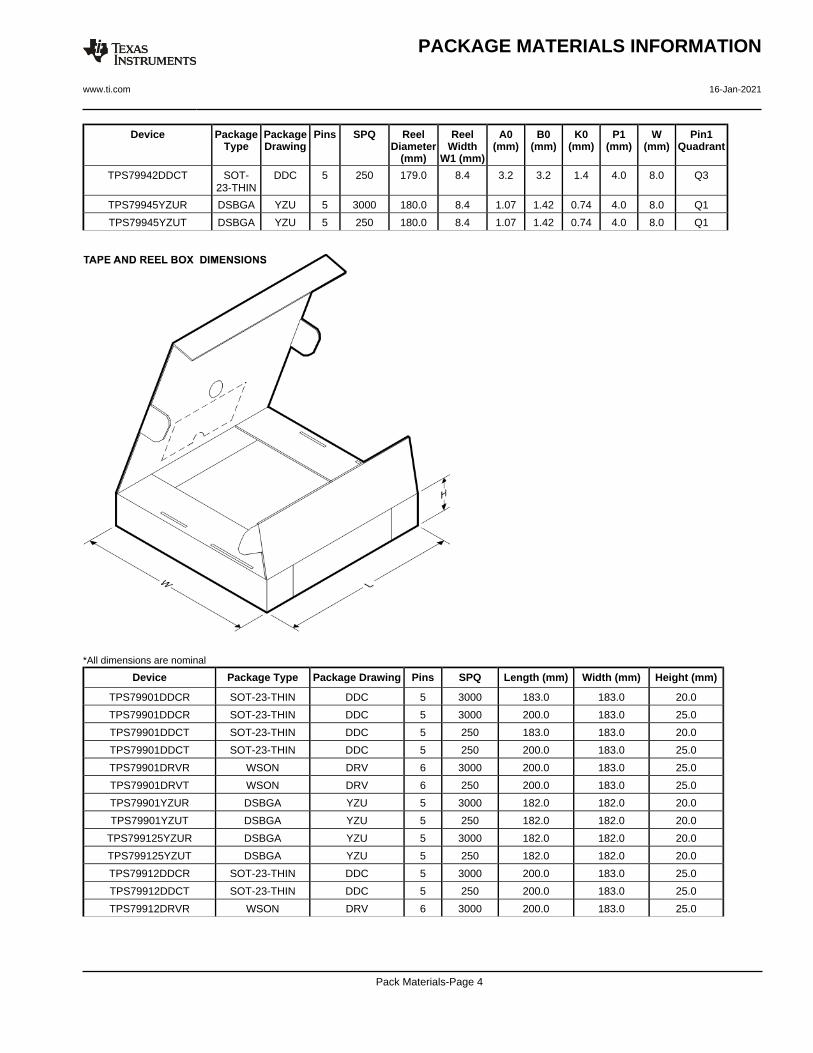
TAPE AND REEL INFORMATION
*All dimensions are nominal
Device PackageType
PackageDrawing
Pins SPQ ReelDiameter
(mm)
ReelWidth
W1 (mm)
A0(mm)
B0(mm)
K0(mm)
P1(mm)
W(mm)
Pin1Quadrant
TPS79901DDCR SOT-23-THIN
DDC 5 3000 180.0 8.4 3.1 3.05 1.1 4.0 8.0 Q3
TPS79901DDCR SOT-23-THIN
DDC 5 3000 179.0 8.4 3.2 3.2 1.4 4.0 8.0 Q3
TPS79901DDCT SOT-23-THIN
DDC 5 250 180.0 8.4 3.1 3.05 1.1 4.0 8.0 Q3
TPS79901DDCT SOT-23-THIN
DDC 5 250 179.0 8.4 3.2 3.2 1.4 4.0 8.0 Q3
TPS79901DRVR WSON DRV 6 3000 179.0 8.4 2.2 2.2 1.2 4.0 8.0 Q2
TPS79901DRVT WSON DRV 6 250 179.0 8.4 2.2 2.2 1.2 4.0 8.0 Q2
TPS79901YZUR DSBGA YZU 5 3000 180.0 8.4 1.07 1.42 0.74 4.0 8.0 Q1
TPS79901YZUT DSBGA YZU 5 250 180.0 8.4 1.07 1.42 0.74 4.0 8.0 Q1
TPS799125YZUR DSBGA YZU 5 3000 180.0 8.4 1.07 1.42 0.74 4.0 8.0 Q1
TPS799125YZUT DSBGA YZU 5 250 180.0 8.4 1.07 1.42 0.74 4.0 8.0 Q1
TPS79912DDCR SOT-23-THIN
DDC 5 3000 179.0 8.4 3.2 3.2 1.4 4.0 8.0 Q3
TPS79912DDCT SOT-23-THIN
DDC 5 250 179.0 8.4 3.2 3.2 1.4 4.0 8.0 Q3
TPS79912DRVR WSON DRV 6 3000 179.0 8.4 2.2 2.2 1.2 4.0 8.0 Q2
TPS79912DRVT WSON DRV 6 250 179.0 8.4 2.2 2.2 1.2 4.0 8.0 Q2
PACKAGE MATERIALS INFORMATION
www.ti.com 16-Jan-2021
Pack Materials-Page 1

Device PackageType
PackageDrawing
Pins SPQ ReelDiameter
(mm)
ReelWidth
W1 (mm)
A0(mm)
B0(mm)
K0(mm)
P1(mm)
W(mm)
Pin1Quadrant
TPS79912YZUR DSBGA YZU 5 3000 180.0 8.4 1.07 1.42 0.74 4.0 8.0 Q1
TPS79912YZUT DSBGA YZU 5 250 180.0 8.4 1.07 1.42 0.74 4.0 8.0 Q1
TPS79913DDCR SOT-23-THIN
DDC 5 3000 179.0 8.4 3.2 3.2 1.4 4.0 8.0 Q3
TPS79913DDCT SOT-23-THIN
DDC 5 250 179.0 8.4 3.2 3.2 1.4 4.0 8.0 Q3
TPS79913YZUR DSBGA YZU 5 3000 180.0 8.4 1.07 1.42 0.74 4.0 8.0 Q1
TPS79915DDCR SOT-23-THIN
DDC 5 3000 179.0 8.4 3.2 3.2 1.4 4.0 8.0 Q3
TPS79915DDCT SOT-23-THIN
DDC 5 250 179.0 8.4 3.2 3.2 1.4 4.0 8.0 Q3
TPS79915YZUR DSBGA YZU 5 3000 180.0 8.4 1.07 1.42 0.74 4.0 8.0 Q1
TPS79915YZUT DSBGA YZU 5 250 180.0 8.4 1.07 1.42 0.74 4.0 8.0 Q1
TPS799185DDCR SOT-23-THIN
DDC 5 3000 179.0 8.4 3.2 3.2 1.4 4.0 8.0 Q3
TPS799185DDCT SOT-23-THIN
DDC 5 250 179.0 8.4 3.2 3.2 1.4 4.0 8.0 Q3
TPS799185YZUR DSBGA YZU 5 3000 180.0 8.4 1.07 1.42 0.74 4.0 8.0 Q1
TPS799185YZUT DSBGA YZU 5 250 180.0 8.4 1.07 1.42 0.74 4.0 8.0 Q1
TPS79918DDCR SOT-23-THIN
DDC 5 3000 179.0 8.4 3.2 3.2 1.4 4.0 8.0 Q3
TPS79918DDCT SOT-23-THIN
DDC 5 250 179.0 8.4 3.2 3.2 1.4 4.0 8.0 Q3
TPS79918DRVR WSON DRV 6 3000 179.0 8.4 2.2 2.2 1.2 4.0 8.0 Q2
TPS79918DRVT WSON DRV 6 250 179.0 8.4 2.2 2.2 1.2 4.0 8.0 Q2
TPS79918YZUR DSBGA YZU 5 3000 180.0 8.4 1.07 1.42 0.74 4.0 8.0 Q1
TPS79918YZUT DSBGA YZU 5 250 180.0 8.4 1.07 1.42 0.74 4.0 8.0 Q1
TPS799195DRVR WSON DRV 6 3000 179.0 8.4 2.2 2.2 1.2 4.0 8.0 Q2
TPS799195DRVT WSON DRV 6 250 179.0 8.4 2.2 2.2 1.2 4.0 8.0 Q2
TPS799195YZUR DSBGA YZU 5 3000 180.0 8.4 1.07 1.42 0.74 4.0 8.0 Q1
TPS799195YZUT DSBGA YZU 5 250 180.0 8.4 1.07 1.42 0.74 4.0 8.0 Q1
TPS79919YZUT DSBGA YZU 5 250 180.0 8.4 1.07 1.42 0.74 4.0 8.0 Q1
TPS79920YZUT DSBGA YZU 5 250 180.0 8.4 1.07 1.42 0.74 4.0 8.0 Q1
TPS79921YZUR DSBGA YZU 5 3000 180.0 8.4 1.07 1.42 0.74 4.0 8.0 Q1
TPS79925DDCR SOT-23-THIN
DDC 5 3000 179.0 8.4 3.2 3.2 1.4 4.0 8.0 Q3
TPS79925DDCT SOT-23-THIN
DDC 5 250 179.0 8.4 3.2 3.2 1.4 4.0 8.0 Q3
TPS79925YZUR DSBGA YZU 5 3000 180.0 8.4 1.07 1.42 0.74 4.0 8.0 Q1
TPS79925YZUT DSBGA YZU 5 250 180.0 8.4 1.07 1.42 0.74 4.0 8.0 Q1
TPS79926YZUR DSBGA YZU 5 3000 180.0 8.4 1.07 1.42 0.74 4.0 8.0 Q1
TPS79926YZUT DSBGA YZU 5 250 180.0 8.4 1.07 1.42 0.74 4.0 8.0 Q1
TPS79927DDCR SOT-23-THIN
DDC 5 3000 179.0 8.4 3.2 3.2 1.4 4.0 8.0 Q3
TPS79927DDCT SOT-23-THIN
DDC 5 250 179.0 8.4 3.2 3.2 1.4 4.0 8.0 Q3
PACKAGE MATERIALS INFORMATION
www.ti.com 16-Jan-2021
Pack Materials-Page 2

Device PackageType
PackageDrawing
Pins SPQ ReelDiameter
(mm)
ReelWidth
W1 (mm)
A0(mm)
B0(mm)
K0(mm)
P1(mm)
W(mm)
Pin1Quadrant
TPS79927DRVR WSON DRV 6 3000 179.0 8.4 2.2 2.2 1.2 4.0 8.0 Q2
TPS79927DRVT WSON DRV 6 250 179.0 8.4 2.2 2.2 1.2 4.0 8.0 Q2
TPS79927YZUT DSBGA YZU 5 250 180.0 8.4 1.07 1.42 0.74 4.0 8.0 Q1
TPS799285DDCR SOT-23-THIN
DDC 5 3000 179.0 8.4 3.2 3.2 1.4 4.0 8.0 Q3
TPS799285DDCT SOT-23-THIN
DDC 5 250 179.0 8.4 3.2 3.2 1.4 4.0 8.0 Q3
TPS799285DRVR WSON DRV 6 3000 179.0 8.4 2.2 2.2 1.2 4.0 8.0 Q2
TPS799285DRVT WSON DRV 6 250 179.0 8.4 2.2 2.2 1.2 4.0 8.0 Q2
TPS799285YZUR DSBGA YZU 5 3000 180.0 8.4 1.07 1.42 0.74 4.0 8.0 Q1
TPS79928DDCR SOT-23-THIN
DDC 5 3000 179.0 8.4 3.2 3.2 1.4 4.0 8.0 Q3
TPS79928DDCT SOT-23-THIN
DDC 5 250 179.0 8.4 3.2 3.2 1.4 4.0 8.0 Q3
TPS79928DRVR WSON DRV 6 3000 179.0 8.4 2.2 2.2 1.2 4.0 8.0 Q2
TPS79928DRVT WSON DRV 6 250 179.0 8.4 2.2 2.2 1.2 4.0 8.0 Q2
TPS79928YZUR DSBGA YZU 5 3000 180.0 8.4 1.07 1.42 0.74 4.0 8.0 Q1
TPS79928YZUT DSBGA YZU 5 250 180.0 8.4 1.07 1.42 0.74 4.0 8.0 Q1
TPS79930DDCR SOT-23-THIN
DDC 5 3000 179.0 8.4 3.2 3.2 1.4 4.0 8.0 Q3
TPS79930DDCR SOT-23-THIN
DDC 5 3000 180.0 8.4 3.1 3.05 1.1 4.0 8.0 Q3
TPS79930DDCT SOT-23-THIN
DDC 5 250 179.0 8.4 3.2 3.2 1.4 4.0 8.0 Q3
TPS79930YZUR DSBGA YZU 5 3000 180.0 8.4 1.07 1.42 0.74 4.0 8.0 Q1
TPS79930YZUT DSBGA YZU 5 250 180.0 8.4 1.07 1.42 0.74 4.0 8.0 Q1
TPS799315DDCR SOT-23-THIN
DDC 5 3000 179.0 8.4 3.2 3.2 1.4 4.0 8.0 Q3
TPS799315DDCT SOT-23-THIN
DDC 5 250 179.0 8.4 3.2 3.2 1.4 4.0 8.0 Q3
TPS799315YZUR DSBGA YZU 5 3000 180.0 8.4 1.07 1.42 0.74 4.0 8.0 Q1
TPS799315YZUT DSBGA YZU 5 250 180.0 8.4 1.07 1.42 0.74 4.0 8.0 Q1
TPS79932YZUR DSBGA YZU 5 3000 180.0 8.4 1.07 1.42 0.74 4.0 8.0 Q1
TPS79933DDCR SOT-23-THIN
DDC 5 3000 179.0 8.4 3.2 3.2 1.4 4.0 8.0 Q3
TPS79933DDCR SOT-23-THIN
DDC 5 3000 180.0 8.4 3.1 3.05 1.1 4.0 8.0 Q3
TPS79933DDCT SOT-23-THIN
DDC 5 250 179.0 8.4 3.2 3.2 1.4 4.0 8.0 Q3
TPS79933DDCT SOT-23-THIN
DDC 5 250 180.0 8.4 3.1 3.05 1.1 4.0 8.0 Q3
TPS79933DRVR WSON DRV 6 3000 179.0 8.4 2.2 2.2 1.2 4.0 8.0 Q2
TPS79933DRVT WSON DRV 6 250 179.0 8.4 2.2 2.2 1.2 4.0 8.0 Q2
TPS79933YZUR DSBGA YZU 5 3000 180.0 8.4 1.07 1.42 0.74 4.0 8.0 Q1
TPS79933YZUT DSBGA YZU 5 250 180.0 8.4 1.07 1.42 0.74 4.0 8.0 Q1
TPS79942DDCR SOT-23-THIN
DDC 5 3000 179.0 8.4 3.2 3.2 1.4 4.0 8.0 Q3
PACKAGE MATERIALS INFORMATION
www.ti.com 16-Jan-2021
Pack Materials-Page 3
Device PackageType
PackageDrawing
Pins SPQ ReelDiameter
(mm)
ReelWidth
W1 (mm)
A0(mm)
B0(mm)
K0(mm)
P1(mm)
W(mm)
Pin1Quadrant
TPS79942DDCT SOT-23-THIN
DDC 5 250 179.0 8.4 3.2 3.2 1.4 4.0 8.0 Q3
TPS79945YZUR DSBGA YZU 5 3000 180.0 8.4 1.07 1.42 0.74 4.0 8.0 Q1
TPS79945YZUT DSBGA YZU 5 250 180.0 8.4 1.07 1.42 0.74 4.0 8.0 Q1
*All dimensions are nominal
Device Package Type Package Drawing Pins SPQ Length (mm) Width (mm) Height (mm)
TPS79901DDCR SOT-23-THIN DDC 5 3000 183.0 183.0 20.0
TPS79901DDCR SOT-23-THIN DDC 5 3000 200.0 183.0 25.0
TPS79901DDCT SOT-23-THIN DDC 5 250 183.0 183.0 20.0
TPS79901DDCT SOT-23-THIN DDC 5 250 200.0 183.0 25.0
TPS79901DRVR WSON DRV 6 3000 200.0 183.0 25.0
TPS79901DRVT WSON DRV 6 250 200.0 183.0 25.0
TPS79901YZUR DSBGA YZU 5 3000 182.0 182.0 20.0
TPS79901YZUT DSBGA YZU 5 250 182.0 182.0 20.0
TPS799125YZUR DSBGA YZU 5 3000 182.0 182.0 20.0
TPS799125YZUT DSBGA YZU 5 250 182.0 182.0 20.0
TPS79912DDCR SOT-23-THIN DDC 5 3000 200.0 183.0 25.0
TPS79912DDCT SOT-23-THIN DDC 5 250 200.0 183.0 25.0
TPS79912DRVR WSON DRV 6 3000 200.0 183.0 25.0
PACKAGE MATERIALS INFORMATION
www.ti.com 16-Jan-2021
Pack Materials-Page 4

Device Package Type Package Drawing Pins SPQ Length (mm) Width (mm) Height (mm)
TPS79912DRVT WSON DRV 6 250 200.0 183.0 25.0
TPS79912YZUR DSBGA YZU 5 3000 182.0 182.0 20.0
TPS79912YZUT DSBGA YZU 5 250 182.0 182.0 20.0
TPS79913DDCR SOT-23-THIN DDC 5 3000 200.0 183.0 25.0
TPS79913DDCT SOT-23-THIN DDC 5 250 200.0 183.0 25.0
TPS79913YZUR DSBGA YZU 5 3000 182.0 182.0 20.0
TPS79915DDCR SOT-23-THIN DDC 5 3000 200.0 183.0 25.0
TPS79915DDCT SOT-23-THIN DDC 5 250 200.0 183.0 25.0
TPS79915YZUR DSBGA YZU 5 3000 182.0 182.0 20.0
TPS79915YZUT DSBGA YZU 5 250 182.0 182.0 20.0
TPS799185DDCR SOT-23-THIN DDC 5 3000 200.0 183.0 25.0
TPS799185DDCT SOT-23-THIN DDC 5 250 200.0 183.0 25.0
TPS799185YZUR DSBGA YZU 5 3000 182.0 182.0 20.0
TPS799185YZUT DSBGA YZU 5 250 182.0 182.0 20.0
TPS79918DDCR SOT-23-THIN DDC 5 3000 200.0 183.0 25.0
TPS79918DDCT SOT-23-THIN DDC 5 250 200.0 183.0 25.0
TPS79918DRVR WSON DRV 6 3000 200.0 183.0 25.0
TPS79918DRVT WSON DRV 6 250 200.0 183.0 25.0
TPS79918YZUR DSBGA YZU 5 3000 182.0 182.0 20.0
TPS79918YZUT DSBGA YZU 5 250 182.0 182.0 20.0
TPS799195DRVR WSON DRV 6 3000 203.0 203.0 35.0
TPS799195DRVT WSON DRV 6 250 203.0 203.0 35.0
TPS799195YZUR DSBGA YZU 5 3000 182.0 182.0 20.0
TPS799195YZUT DSBGA YZU 5 250 182.0 182.0 20.0
TPS79919YZUT DSBGA YZU 5 250 182.0 182.0 20.0
TPS79920YZUT DSBGA YZU 5 250 182.0 182.0 20.0
TPS79921YZUR DSBGA YZU 5 3000 210.0 185.0 35.0
TPS79925DDCR SOT-23-THIN DDC 5 3000 200.0 183.0 25.0
TPS79925DDCT SOT-23-THIN DDC 5 250 200.0 183.0 25.0
TPS79925YZUR DSBGA YZU 5 3000 182.0 182.0 20.0
TPS79925YZUT DSBGA YZU 5 250 182.0 182.0 20.0
TPS79926YZUR DSBGA YZU 5 3000 182.0 182.0 20.0
TPS79926YZUT DSBGA YZU 5 250 182.0 182.0 20.0
TPS79927DDCR SOT-23-THIN DDC 5 3000 200.0 183.0 25.0
TPS79927DDCT SOT-23-THIN DDC 5 250 200.0 183.0 25.0
TPS79927DRVR WSON DRV 6 3000 200.0 183.0 25.0
TPS79927DRVT WSON DRV 6 250 203.0 203.0 35.0
TPS79927YZUT DSBGA YZU 5 250 182.0 182.0 20.0
TPS799285DDCR SOT-23-THIN DDC 5 3000 200.0 183.0 25.0
TPS799285DDCT SOT-23-THIN DDC 5 250 200.0 183.0 25.0
TPS799285DRVR WSON DRV 6 3000 200.0 183.0 25.0
TPS799285DRVT WSON DRV 6 250 200.0 183.0 25.0
TPS799285YZUR DSBGA YZU 5 3000 182.0 182.0 20.0
TPS79928DDCR SOT-23-THIN DDC 5 3000 200.0 183.0 25.0
PACKAGE MATERIALS INFORMATION
www.ti.com 16-Jan-2021
Pack Materials-Page 5

Device Package Type Package Drawing Pins SPQ Length (mm) Width (mm) Height (mm)
TPS79928DDCT SOT-23-THIN DDC 5 250 200.0 183.0 25.0
TPS79928DRVR WSON DRV 6 3000 200.0 183.0 25.0
TPS79928DRVT WSON DRV 6 250 200.0 183.0 25.0
TPS79928YZUR DSBGA YZU 5 3000 182.0 182.0 20.0
TPS79928YZUT DSBGA YZU 5 250 182.0 182.0 20.0
TPS79930DDCR SOT-23-THIN DDC 5 3000 200.0 183.0 25.0
TPS79930DDCR SOT-23-THIN DDC 5 3000 183.0 183.0 20.0
TPS79930DDCT SOT-23-THIN DDC 5 250 200.0 183.0 25.0
TPS79930YZUR DSBGA YZU 5 3000 182.0 182.0 20.0
TPS79930YZUT DSBGA YZU 5 250 182.0 182.0 20.0
TPS799315DDCR SOT-23-THIN DDC 5 3000 200.0 183.0 25.0
TPS799315DDCT SOT-23-THIN DDC 5 250 200.0 183.0 25.0
TPS799315YZUR DSBGA YZU 5 3000 182.0 182.0 20.0
TPS799315YZUT DSBGA YZU 5 250 182.0 182.0 20.0
TPS79932YZUR DSBGA YZU 5 3000 182.0 182.0 20.0
TPS79933DDCR SOT-23-THIN DDC 5 3000 200.0 183.0 25.0
TPS79933DDCR SOT-23-THIN DDC 5 3000 183.0 183.0 20.0
TPS79933DDCT SOT-23-THIN DDC 5 250 200.0 183.0 25.0
TPS79933DDCT SOT-23-THIN DDC 5 250 183.0 183.0 20.0
TPS79933DRVR WSON DRV 6 3000 200.0 183.0 25.0
TPS79933DRVT WSON DRV 6 250 200.0 183.0 25.0
TPS79933YZUR DSBGA YZU 5 3000 182.0 182.0 20.0
TPS79933YZUT DSBGA YZU 5 250 182.0 182.0 20.0
TPS79942DDCR SOT-23-THIN DDC 5 3000 200.0 183.0 25.0
TPS79942DDCT SOT-23-THIN DDC 5 250 200.0 183.0 25.0
TPS79945YZUR DSBGA YZU 5 3000 182.0 182.0 20.0
TPS79945YZUT DSBGA YZU 5 250 182.0 182.0 20.0
PACKAGE MATERIALS INFORMATION
www.ti.com 16-Jan-2021
Pack Materials-Page 6

GENERIC PACKAGE VIEW
Images above are just a representation of the package family, actual package may vary.Refer to the product data sheet for package details.
DRV 6 WSON - 0.8 mm max heightPLASTIC SMALL OUTLINE - NO LEAD
4206925/F

www.ti.com
PACKAGE OUTLINE
C
6X 0.350.25
1.6 0.1
6X 0.30.2
2X1.3
1 0.1
4X 0.65
0.80.7
0.050.00
B 2.11.9
A
2.11.9
(0.2) TYP
WSON - 0.8 mm max heightDRV0006APLASTIC SMALL OUTLINE - NO LEAD
4222173/B 04/2018
PIN 1 INDEX AREA
SEATING PLANE
0.08 C
1
34
6
(OPTIONAL)PIN 1 ID
0.1 C A B0.05 C
THERMAL PADEXPOSED
7
NOTES: 1. All linear dimensions are in millimeters. Any dimensions in parenthesis are for reference only. Dimensioning and tolerancing per ASME Y14.5M. 2. This drawing is subject to change without notice. 3. The package thermal pad must be soldered to the printed circuit board for thermal and mechanical performance.
SCALE 5.500

www.ti.com
EXAMPLE BOARD LAYOUT
0.07 MINALL AROUND
0.07 MAXALL AROUND
(1)
4X (0.65)
(1.95)
6X (0.3)
6X (0.45)
(1.6)
(R0.05) TYP
( 0.2) VIATYP
(1.1)
WSON - 0.8 mm max heightDRV0006APLASTIC SMALL OUTLINE - NO LEAD
4222173/B 04/2018
SYMM
1
34
6
SYMM
LAND PATTERN EXAMPLESCALE:25X
7
NOTES: (continued) 4. This package is designed to be soldered to a thermal pad on the board. For more information, see Texas Instruments literature number SLUA271 (www.ti.com/lit/slua271).5. Vias are optional depending on application, refer to device data sheet. If some or all are implemented, recommended via locations are shown.
SOLDER MASKOPENINGSOLDER MASK
METAL UNDER
SOLDER MASKDEFINED
METALSOLDER MASKOPENING
SOLDER MASK DETAILS
NON SOLDER MASKDEFINED
(PREFERRED)

www.ti.com
EXAMPLE STENCIL DESIGN
6X (0.3)
6X (0.45)
4X (0.65)
(0.7)
(1)
(1.95)
(R0.05) TYP
(0.45)
WSON - 0.8 mm max heightDRV0006APLASTIC SMALL OUTLINE - NO LEAD
4222173/B 04/2018
NOTES: (continued) 6. Laser cutting apertures with trapezoidal walls and rounded corners may offer better paste release. IPC-7525 may have alternate design recommendations.
SOLDER PASTE EXAMPLEBASED ON 0.125 mm THICK STENCIL
EXPOSED PAD #7
88% PRINTED SOLDER COVERAGE BY AREA UNDER PACKAGESCALE:30X
SYMM
1
3 4
6
SYMM
METAL7

www.ti.com
PACKAGE OUTLINE
C
6X 0.350.25
1.6 0.1
6X 0.30.2
2X1.3
1 0.1
4X 0.65
0.80.7
0.050.00
B 2.11.9
A
2.11.9
(0.2) TYP
WSON - 0.8 mm max heightDRV0006DPLASTIC SMALL OUTLINE - NO LEAD
4225563/A 12/2019
PIN 1 INDEX AREA
SEATING PLANE
0.08 C
1
34
6
(OPTIONAL)PIN 1 ID
0.1 C A B0.05 C
THERMAL PADEXPOSED
7
NOTES: 1. All linear dimensions are in millimeters. Any dimensions in parenthesis are for reference only. Dimensioning and tolerancing per ASME Y14.5M. 2. This drawing is subject to change without notice. 3. The package thermal pad must be soldered to the printed circuit board for thermal and mechanical performance.
SCALE 5.500

www.ti.com
EXAMPLE BOARD LAYOUT
0.07 MINALL AROUND
0.07 MAXALL AROUND
(1)
4X (0.65)
(1.95)
6X (0.3)
6X (0.45)
(1.6)
(R0.05) TYP
( 0.2) VIATYP
(1.1)
WSON - 0.8 mm max heightDRV0006DPLASTIC SMALL OUTLINE - NO LEAD
4225563/A 12/2019
SYMM
1
34
6
SYMM
LAND PATTERN EXAMPLEEXPOSED METAL SHOWN
SCALE:25X
7
NOTES: (continued) 4. This package is designed to be soldered to a thermal pad on the board. For more information, see Texas Instruments literature number SLUA271 (www.ti.com/lit/slua271).5. Vias are optional depending on application, refer to device data sheet. If some or all are implemented, recommended via locations are shown.
SOLDER MASKOPENINGSOLDER MASK
METAL UNDER
SOLDER MASKDEFINED
EXPOSEDMETAL
METALSOLDER MASKOPENING
SOLDER MASK DETAILS
NON SOLDER MASKDEFINED
(PREFERRED)
EXPOSEDMETAL

www.ti.com
EXAMPLE STENCIL DESIGN
6X (0.3)
6X (0.45)
4X (0.65)
(0.7)
(1)
(1.95)
(R0.05) TYP
(0.45)
WSON - 0.8 mm max heightDRV0006DPLASTIC SMALL OUTLINE - NO LEAD
4225563/A 12/2019
NOTES: (continued) 6. Laser cutting apertures with trapezoidal walls and rounded corners may offer better paste release. IPC-7525 may have alternate design recommendations.
SOLDER PASTE EXAMPLEBASED ON 0.125 mm THICK STENCIL
EXPOSED PAD #7
88% PRINTED SOLDER COVERAGE BY AREA UNDER PACKAGESCALE:30X
SYMM
1
3 4
6
SYMM
METAL7


www.ti.com
PACKAGE OUTLINE
C0.625 MAX
0.30.2
0.5 TYP
5X 0.350.25
0.5 TYP
0.433
B E A
D
4222196/A 11/2015
DSBGA - 0.625 mm max heightYZU0005DIE SIZE BALL GRID ARRAY
NOTES: 1. All linear dimensions are in millimeters. Any dimensions in parenthesis are for reference only. Dimensioning and tolerancing per ASME Y14.5M.2. This drawing is subject to change without notice.
3
SYMM
SYMM
BALL A1CORNER
SEATING PLANE
BALL TYP 0.05 C
C
B
A
1 2
0.015 C A B
SCALE 10.000
D: Max =
E: Max =
1.367 mm, Min =
1.001 mm, Min =
1.307 mm
0.94 mm

www.ti.com
EXAMPLE BOARD LAYOUT
5X ( )0.25
(0.5) TYP
(0.433) TYP
( )METAL
0.25 0.05 MAX
SOLDER MASKOPENING
METAL UNDERSOLDER MASK
( )SOLDER MASKOPENING
0.25
0.05 MIN
4222196/A 11/2015
DSBGA - 0.625 mm max heightYZU0005DIE SIZE BALL GRID ARRAY
NOTES: (continued) 3. Final dimensions may vary due to manufacturing tolerance considerations and also routing constraints. Refer to Texas Instruments Literature No. SNVA009 (www.ti.com/lit/snva009).
SOLDER MASK DETAILSNOT TO SCALE
1 3
SYMM
SYMM
LAND PATTERN EXAMPLESCALE:50X
C
2
A
B
NON-SOLDER MASKDEFINED
(PREFERRED)SOLDER MASK
DEFINED

www.ti.com
EXAMPLE STENCIL DESIGN
(0.433) TYP
(0.5) TYP
5X ( 0.25)(R ) TYP0.05
METALTYP
4222196/A 11/2015
DSBGA - 0.625 mm max heightYZU0005DIE SIZE BALL GRID ARRAY
NOTES: (continued) 4. Laser cutting apertures with trapezoidal walls and rounded corners may offer better paste release.
C
1 2
A
B
3
SYMM
SYMM
SOLDER PASTE EXAMPLEBASED ON 0.1 mm THICK STENCIL
SCALE:50X

IMPORTANT NOTICE AND DISCLAIMERTI PROVIDES TECHNICAL AND RELIABILITY DATA (INCLUDING DATASHEETS), DESIGN RESOURCES (INCLUDING REFERENCEDESIGNS), APPLICATION OR OTHER DESIGN ADVICE, WEB TOOLS, SAFETY INFORMATION, AND OTHER RESOURCES “AS IS”AND WITH ALL FAULTS, AND DISCLAIMS ALL WARRANTIES, EXPRESS AND IMPLIED, INCLUDING WITHOUT LIMITATION ANYIMPLIED WARRANTIES OF MERCHANTABILITY, FITNESS FOR A PARTICULAR PURPOSE OR NON-INFRINGEMENT OF THIRDPARTY INTELLECTUAL PROPERTY RIGHTS.These resources are intended for skilled developers designing with TI products. You are solely responsible for (1) selecting the appropriateTI products for your application, (2) designing, validating and testing your application, and (3) ensuring your application meets applicablestandards, and any other safety, security, or other requirements. These resources are subject to change without notice. TI grants youpermission to use these resources only for development of an application that uses the TI products described in the resource. Otherreproduction and display of these resources is prohibited. No license is granted to any other TI intellectual property right or to any third partyintellectual property right. TI disclaims responsibility for, and you will fully indemnify TI and its representatives against, any claims, damages,costs, losses, and liabilities arising out of your use of these resources.TI’s products are provided subject to TI’s Terms of Sale (https:www.ti.com/legal/termsofsale.html) or other applicable terms available eitheron ti.com or provided in conjunction with such TI products. TI’s provision of these resources does not expand or otherwise alter TI’sapplicable warranties or warranty disclaimers for TI products.IMPORTANT NOTICE
Mailing Address: Texas Instruments, Post Office Box 655303, Dallas, Texas 75265Copyright © 2021, Texas Instruments Incorporated