Embed Size (px)
Citation preview

LT3045
13045f
For more information www.linear.com/LT3045
Typical applicaTion
FeaTures DescripTion
20V, 500mA, Ultralow Noise, Ultrahigh PSRR Linear Regulator
The LT®3045 is a high performance low dropout linear regulator featuring LTC’s ultralow noise and ultrahigh PSRR architecture for powering noise sensitive applica-tions. Designed as a precision current reference followed by a high performance voltage buffer, the LT3045 can be easily paralleled to further reduce noise, increase output current and spread heat on the PCB.
The device supplies 500mA at a typical 260mV dropout voltage. Operating quiescent current is nominally 2.2mA and drops to <<1µA in shutdown. The LT3045’s wide output voltage range (0V to 15V) while maintaining unity-gain operation provides virtually constant output noise, PSRR, bandwidth and load regulation, independent of the programmed output voltage. Additionally, the regulator features programmable current limit, fast start-up capa-bility and programmable power good to indicate output voltage regulation.
The LT3045 is stable with a minimum 10µF ceramic output capacitor. Built-in protection includes reverse battery protection, reverse current protection, internal current limit with foldback and thermal limit with hysteresis. The LT3045 is available in thermally enhanced 12-Lead MSOP and 10-Lead 3mm × 3mm DFN packages.
Power Supply Ripple Rejection
applicaTions
n Ultralow RMS Noise: 0.8µVRMS (10Hz to 100kHz) n Ultralow Spot Noise: 2nV/√Hz at 10kHz n Ultrahigh PSRR: 76dB at 1MHz n Output Current: 500mA n Wide Input Voltage Range: 1.8V to 20V n Single Capacitor Improves Noise and PSRR n 100µA SET Pin Current: ±1% Initial Accuracy n Single Resistor Programs Output Voltage n High Bandwidth: 1MHz n Programmable Current Limit n Low Dropout Voltage: 260mV n Output Voltage Range: 0V to 15V n Programmable Power Good n Fast Start-Up Capability n Precision Enable/UVLO n Parallelable for Lower Noise and Higher Current n Internal Current Limit with Foldback n Minimum Output Capacitor: 10µF Ceramic n Reverse Battery and Reverse Current Protection n 12-Lead MSOP and 10-Lead 3mm × 3mm DFN Packages
n RF Power Supplies: PLLs, VCOs, Mixers, LNAs, PAs n Very Low Noise Instrumentation n High Speed/High Precision Data Converters n Medical Applications: Imaging, Diagnostics n Precision Power Supplies n Post-Regulator for Switching Supplies
L, LT, LTC, LTM, Linear Technology and the Linear logo are registered trademarks of Linear Technology Corporation. Patents pending. All other trademarks are the property of their respective owners.
VIN = 5VRSET = 30.1kCSET = 4.7µFCOUT = 10µFIL = 500mA
FREQUENCY (Hz)10 100 1k 10k 100k 1M 10M
20
30
40
50
60
70
80
90
100
110
120
PSRR
(dB)
3045 TA01b
+–
100µA
IN
EN/UV
PG
GND
OUT
LT3045
ILIM PGFB402k
10µF
4.7µF*
*OPTIONAL, SEE APPLICATIONS INFORMATION
VIN5V ±5%
200k
4.7µF
VOUT3VIOUT(MAX)500mA
49.9k
3045 TA01a
249Ω30.1k
SET
OUTS

LT3045
23045f
For more information www.linear.com/LT3045
pin conFiguraTion
absoluTe MaxiMuM raTingsIN Pin Voltage .........................................................±22VEN/UV Pin Voltage ..................................................±22VIN-to-EN/UV Differential..........................................±22VPG Pin Voltage (Note 10) ...............................–0.3V, 22VILIM Pin Voltage (Note 10) ...............................–0.3V, 1VPGFB Pin Voltage (Note 10) ...........................–0.3V, 22VSET Pin Voltage (Note 10) ..............................–0.3V, 16VSET Pin Current (Note 7) .................................... ±20mAOUTS Pin Voltage (Note 10) ...........................–0.3V, 16VOUTS Pin Current (Note 7) ................................. ±20mA
(Note 1)
TOP VIEW
11GND
DD PACKAGE10-LEAD (3mm × 3mm) PLASTIC DFN
10
9
6
7
8
4
5
3
2
1 OUT
OUTS
GND
SET
PGFB
IN
IN
EN/UV
PG
ILIM
TJMAX = 150°C, θJA = 34°C/W, θJC = 5.5°C/W
EXPOSED PAD (PIN 11) IS GND, MUST BE SOLDERED TO PCB
123456
INININ
EN/UVPG
ILIM
121110987
OUTOUTOUTSGNDSETPGFB
TOP VIEW
MSE PACKAGE12-LEAD PLASTIC MSOP
13GND
TJMAX = 150°C, θJA = 33°C/W, θJC = 8°C/W
EXPOSED PAD (PIN 13) IS GND, MUST BE SOLDERED TO PCB
orDer inForMaTionLEAD FREE FINISH TAPE AND REEL PART MARKING* PACKAGE DESCRIPTION TEMPERATURE RANGE
LT3045EDD#PBF LT3045EDD#TRPBF LGYP 10-Lead (3mm × 3mm) Plastic DFN –40°C to 125°C
LT3045IDD#PBF LT3045IDD#TRPBF LGYP 10-Lead (3mm × 3mm) Plastic DFN –40°C to 125°C
LT3045EMSE#PBF LT3045EMSE#TRPBF 3045 12-Lead Plastic MSOP –40°C to 125°C
LT3045IMSE#PBF LT3045IMSE#TRPBF 3045 12-Lead Plastic MSOP –40°C to 125°C
Consult LTC Marketing for parts specified with wider operating temperature ranges. *The temperature grade is identified by a label on the shipping container.For more information on lead free part marking, go to: http://www.linear.com/leadfree/ For more information on tape and reel specifications, go to: http://www.linear.com/tapeandreel/. Some packages are available in 500 unit reels through designated sales channels with #TRMPBF suffix.
OUT Pin Voltage (Note 10) .............................–0.3V, 16VOUT-to-OUTS Differential (Note 14) ....................... ±1.2VIN-to-OUT Differential .............................................±22VIN-to-OUTS Differential ...........................................±22VOutput Short-Circuit Duration .......................... IndefiniteOperating Junction Temperature Range (Note 9)
E-Grade, I-Grade ............................... –40°C to 125°C Storage Temperature Range .............. –65°C to 150°C
Lead Temperature (Soldering, 10 Sec) MSE Package ................................................... 300°C
http://www.linear.com/product/LT3045#orderinfo

LT3045
33045f
For more information www.linear.com/LT3045
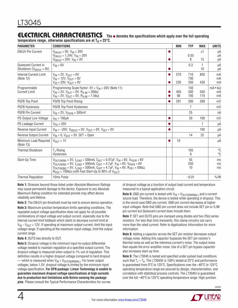
elecTrical characTerisTics The l denotes the specifications which apply over the full operating temperature range, otherwise specifications are at TA = 25°C.PARAMETER CONDITIONS MIN TYP MAX UNITSInput Voltage Range l 2 20 V
Minimum IN Pin Voltage (Note 2)
ILOAD = 500mA, VIN UVLO Rising VIN UVLO Hysteresis
l 1.78 75
2 V mV
Output Voltage Range VIN > VOUT l 0 15 V
SET Pin Current (ISET) VIN = 2V, ILOAD = 1mA, VOUT = 1.3V 2V < VIN < 20V, 0V < VOUT < 15V, 1mA < ILOAD < 500mA (Note 3)
l
99 98
100 100
101 102
µA µA
Fast Start-Up Set Pin Current
VPGFB = 289mV, VIN = 2.8V, VSET = 1.3V 2 mA
Output Offset Voltage VOS (VOUT – VSET) (Note 4)
VIN = 2V, ILOAD = 1mA, VOUT = 1.3V 2V < VIN < 20V, 0V < VOUT < 15V, 1mA < ILOAD < 500mA (Note 3)
l
–1 –2
1 2
mV mV
Line Regulation: ∆ISET Line Regulation: ∆VOS
VIN = 2V to 20V, ILOAD = 1mA, VOUT = 1.3V VIN = 2V to 20V, ILOAD = 1mA, VOUT = 1.3V (Note 4)
l
l
0.5 0.5
±2 ±3
nA/V µV/V
Load Regulation: ∆ISET Load Regulation: ∆VOS
ILOAD = 1mA to 500mA, VIN = 2V, VOUT = 1.3V ILOAD = 1mA to 500mA, VIN = 2V, VOUT = 1.3V (Note 4)
l
3 0.1
0.5
nA mV
Change in ISET with VSET Change in VOS with VSET Change in ISET with VSET Change in VOS with VSET
VSET = 1.3V to 15V, VIN = 20V, ILOAD = 1mA VSET = 1.3V to 15V, VIN = 20V, ILOAD = 1mA (Note 4) VSET = 0V to 1.3V, VIN = 20V, ILOAD = 1mA VSET = 0V to 1.3V, VIN = 20V, ILOAD = 1mA (Note 4)
l
l
l
l
30 0.03 150 0.3
400 0.6 600
2
nA mV nA
mV
Dropout Voltage ILOAD = 1mA, 50mA
l
220 275 330
mV mV
ILOAD = 300mA (Note 5)
l
220 280 350
mV mV
ILOAD = 500mA (Note 5)
l
260 350 450
mV mV
GND Pin Current VIN = VOUT(NOMINAL) (Note 6)
ILOAD = 10µA ILOAD = 1mA ILOAD = 50mA ILOAD = 100mA ILOAD = 500mA
l
l
l
l
2.2 2.4 3.5 4.3 15
4
5.5 7
25
mA mA mA mA mA
Output Noise Spectral Density (Notes 4, 8)
ILOAD = 500mA, Frequency = 10Hz, COUT = 10µF, CSET = 0.47µF, VOUT = 3.3V ILOAD = 500mA, Frequency = 10Hz, COUT = 10µF, CSET = 4.7µF, 1.3V ≤ VOUT ≤ 15V ILOAD = 500mA, Frequency = 10kHz, COUT = 10µF, CSET = 0.47µF, 1.3V ≤ VOUT ≤ 15V ILOAD = 500mA, Frequency = 10kHz, COUT = 10µF, CSET = 0.47µF, 0V ≤ VOUT < 1.3V
500 70 2 5
nV/√Hz nV/√Hz nV/√Hz nV/√Hz
Output RMS Noise (Notes 4, 8)
ILOAD = 500mA, BW = 10Hz to 100kHz, COUT = 10µF, CSET = 0.47µF, VOUT = 3.3V ILOAD = 500mA, BW = 10Hz to 100kHz, COUT = 10µF, CSET = 4.7µF, 1.3V ≤ VOUT ≤ 15V ILOAD = 500mA, BW = 10Hz to 100kHz, COUT = 10µF, CSET = 4.7µF, 0V ≤ VOUT < 1.3V
2.5 0.8 1.8
µVRMS µVRMS µVRMS
Reference Current RMS Output Noise (Notes 4, 8)
BW = 10Hz to 100kHz 6 nARMS
Ripple Rejection 1.3V ≤ VOUT ≤ 15V VIN – VOUT = 2V (Avg) (Notes 4, 8)
VRIPPLE = 500mVP-P, fRIPPLE = 120Hz, ILOAD = 500mA, COUT = 10µF, CSET = 4.7µF VRIPPLE = 150mVP-P, fRIPPLE = 10kHz, ILOAD = 500mA, COUT = 10µF, CSET = 0.47µF VRIPPLE = 150mVP-P, fRIPPLE = 100kHz, ILOAD = 500mA, COUT = 10µF, CSET = 0.47µF VRIPPLE = 150mVP-P, fRIPPLE = 1MHz, ILOAD = 500mA, COUT = 10µF, CSET = 0.47µF VRIPPLE = 80mVP-P, fRIPPLE = 10MHz, ILOAD = 500mA, COUT = 10µF, CSET = 0.47µF
117 90 77 76 53
dB dB dB dB dB
Ripple Rejection 0V ≤ VOUT < 1.3V VIN – VOUT = 2V (Avg) (Notes 4, 8)
VRIPPLE = 500mVP-P, fRIPPLE = 120Hz, ILOAD = 500mA, COUT = 10µF, CSET = 0.47µF VRIPPLE = 50mVP-P, fRIPPLE = 10kHz, ILOAD = 500mA, COUT = 10µF, CSET = 0.47µF VRIPPLE = 50mVP-P, fRIPPLE = 100kHz, ILOAD = 500mA, COUT = 10µF, CSET = 0.47µF VRIPPLE = 50mVP-P, fRIPPLE = 1MHz, ILOAD = 500mA, COUT = 10µF, CSET = 0.47µF VRIPPLE = 50mVP-P, fRIPPLE = 10MHz, ILOAD = 500mA, COUT = 10µF, CSET = 0.47µF
104 85 72 64 54
dB dB dB dB dB
EN/UV Pin Threshold EN/UV Trip Point Rising (Turn-On), VIN = 2V l 1.18 1.24 1.32 V
EN/UV Pin Hysteresis EN/UV Trip Point Hysteresis, VIN = 2V 130 mV
LT3045
43045f
For more information www.linear.com/LT3045
elecTrical characTerisTics The l denotes the specifications which apply over the full operating temperature range, otherwise specifications are at TA = 25°C.PARAMETER CONDITIONS MIN TYP MAX UNITSEN/UV Pin Current VEN/UV = 0V, VIN = 20V
VEN/UV = 1.24V, VIN = 20V VEN/UV = 20V, VIN = 0V
l
l
0.03
8
±1
15
µA µA µA
Quiescent Current in Shutdown (VEN/UV = 0V)
VIN = 6V
l
0.3 1 10
µA µA
Internal Current Limit (Note 12)
VIN = 2V, VOUT = 0V VIN = 12V, VOUT = 0V VIN = 20V, VOUT = 0V
l
l
570
230
710 700 330
850
430
mA mA mA
Programmable Current Limit
Programming Scale Factor: 2V < VIN < 20V (Note 11) VIN = 2V, VOUT = 0V, RILIM = 300Ω VIN = 2V, VOUT = 0V, RILIM = 1.5kΩ
l
l
450 90
150 500 100
550 110
mA • kΩ mA mA
PGFB Trip Point PGFB Trip Point Rising l 291 300 309 mV
PGFB Hysteresis PGFB Trip Point Hysteresis 7 mV
PGFB Pin Current VIN = 2V, VPGFB = 300mV 25 nA
PG Output Low Voltage IPG = 100µA l 30 100 mV
PG Leakage Current VPG = 20V l 1 µA
Reverse Input Current VIN = –20V, VEN/UV = 0V, VOUT = 0V, VSET = 0V l 100 µA
Reverse Output Current VIN = 0, VOUT = 5V, SET = Open 14 25 µA
Minimum Load Required (Note 13)
VOUT < 1V l 10 µA
Thermal Shutdown TJ Rising Hysteresis
165 8
°C °C
Start-Up Time VOUT(NOM) = 5V, ILOAD = 500mA, CSET = 0.47µF, VIN = 6V, VPGFB = 6V VOUT(NOM) = 5V, ILOAD = 500mA, CSET = 4.7µF, VIN = 6V, VPGFB = 6V VOUT(NOM) = 5V, ILOAD = 500mA, CSET = 4.7µF, VIN = 6V, RPG1 = 50kΩ, RPG2 = 700kΩ (with Fast Start-Up to 90% of VOUT)
55 550 10
ms ms ms
Thermal Regulation 10ms Pulse –0.01 %/W
Note 1: Stresses beyond those listed under Absolute Maximum Ratings may cause permanent damage to the device. Exposure to any Absolute Maximum Rating condition for extended periods may affect device reliability and lifetime.Note 2: The EN/UV pin threshold must be met to ensure device operation.Note 3: Maximum junction temperature limits operating conditions. The regulated output voltage specification does not apply for all possible combinations of input voltage and output current, especially due to the internal current limit foldback which starts to decrease current limit at VIN – VOUT > 12V. If operating at maximum output current, limit the input voltage range. If operating at the maximum input voltage, limit the output current range.Note 4: OUTS ties directly to OUT.Note 5: Dropout voltage is the minimum input-to-output differential voltage needed to maintain regulation at a specified output current. The dropout voltage is measured when output is 1% out of regulation. This definition results in a higher dropout voltage compared to hard dropout — which is measured when VIN = VOUT(NOMINAL). For lower output voltages, below 1.5V, dropout voltage is limited by the minimum input voltage specification. For DFN package: Linear Technology is unable to guarantee maximum dropout voltage specifications at high currents due to production test limitations with Kelvin-sensing the package pins. Please consult the Typical Performance Characteristics for curves
of dropout voltage as a function of output load current and temperature measured in a typical application circuit.Note 6: GND pin current is tested with VIN = VOUT(NOMINAL) and a current source load. Therefore, the device is tested while operating in dropout. This is the worst-case GND pin current. GND pin current decreases at higher input voltages. Note that GND pin current does not include SET pin or ILIM pin current but Quiescent current does include them.Note 7: SET and OUTS pins are clamped using diodes and two 25Ω series resistors. For less than 5ms transients, this clamp circuitry can carry more than the rated current. Refer to Applications Information for more information.Note 8: Adding a capacitor across the SET pin resistor decreases output voltage noise. Adding this capacitor bypasses the SET pin resistor’s thermal noise as well as the reference current’s noise. The output noise then equals the error amplifier noise. Use of a SET pin bypass capacitor also increases start-up time.Note 9: The LT3045 is tested and specified under pulsed load conditions such that TJ ≈ TA. The LT3045E is 100% tested at 25°C and performance is guaranteed from 0°C to 125°C. Specifications over the –40°C to 125°C operating temperature range are assured by design, characterization, and correlation with statistical process controls. The LT3045I is guaranteed over the full –40°C to 125°C operating temperature range. High junction

LT3045
53045f
For more information www.linear.com/LT3045
Typical perForMance characTerisTics
Offset Voltage SET Pin Current Offset Voltage (VOUT – VSET)
SET Pin Current SET Pin Current Offset Voltage (VOUT – VSET)
TJ = 25°C, unless otherwise noted.
elecTrical characTerisTicstemperatures degrade operating lifetimes. Operating lifetime is derated at junction temperatures greater than 125°C.Note 10: Parasitic diodes exist internally between the ILIM, PG, PGFB, SET, OUTS, and OUT pins and the GND pin. Do not drive these pins more than 0.3V below the GND pin during a fault condition. These pins must remain at a voltage more positive than GND during normal operation.Note 11: The current limit programming scale factor is specified while the internal backup current limit is not active. Note that the internal current limit has foldback protection for VIN – VOUT differentials greater than 12V.
Note 12: The internal back-up current limit circuitry incorporates foldback protection that decreases current limit for VIN – VOUT > 12V. Some level of output current is provided at all VIN – VOUT differential voltages. Consult the Typical Performance Characteristics graph for current limit vs VIN – VOUT.Note 13: For output voltages less than 1V, the LT3045 requires a 10µA minimum load current for stability.Note 14: Maximum OUT-to-OUTS differential is guaranteed by design.
VIN = 2VIL = 1mAVOUT = 1.3V
TEMPERATURE (°C)–75 –50 –25 0 25 50 75 100 125 150
99.0
99.2
99.4
99.6
99.8
100.0
100.2
100.4
100.6
100.8
101.0
SET
PIN
CURR
ENT
(µA)
3045 G01
N = 3250
ISET DISTRIBUTION (µA)98 99 100 101 102
3045 G02
VIN = 2VIL = 1mAVOUT = 1.3V
TEMPERATURE (°C)–75 –50 –25 0 25 50 75 100 125 150
–2.0
–1.5
–1.0
–0.5
0
0.5
1.0
1.5
2.0
OFFS
ET V
OLTA
GE (m
V)
3045 G03
N = 3250
VOS DISTRIBUTION (mV)–2 –1 0 1 2
3045 G04
IL = 1mAVOUT = 1.3V
150°C125°C25°C–55°C
INPUT VOLTAGE (V)0 2 4 6 8 10 12 14 16 18 20
99.0
99.2
99.4
99.6
99.8
100.0
100.2
100.4
100.6
100.8
101.0
SET
PIN
CURR
ENT
(µA)
3045 G05
IL = 1mAVOUT = 1.3V
150°C125°C25°C–55°C
INPUT VOLTAGE (V)0 2 4 6 8 10 12 14 16 18 20
–2.0
–1.5
–1.0
–0.5
0
0.5
1.0
1.5
2.0
OFFS
ET V
OLTA
GE (m
V)
3045 G06

LT3045
63045f
For more information www.linear.com/LT3045
Typical perForMance characTerisTics
Quiescent Current Typical Dropout Voltage Dropout Voltage
Quiescent Current Quiescent Current Quiescent Current
TJ = 25°C, unless otherwise noted.
SET Pin Current Offset Voltage (VOUT – VSET) Load Regulation
IL = 1mAVIN = 20V
150°C125°C25°C–55°C
OUTPUT VOLTAGE (V)0 1.5 3 4.5 6 7.5 9 10.5 12 13.5 15
99.0
99.2
99.4
99.6
99.8
100.0
100.2
100.4
100.6
100.8
101.0
SET
PIN
CURR
ENT
(µA)
3045 G07
IL = 1mAVIN = 20V
150°C125°C25°C–55°C
OUTPUT VOLTAGE (V)0 1.5 3 4.5 6 7.5 9 10.5 12 13.5 15
–2.0
–1.5
–1.0
–0.5
0
0.5
1.0
1.5
2.0
OFFS
ET V
OLTA
GE (m
V)
3045 G08
VIN = 2.5V∆IL= 1mA to 500mAVOUT = 1.3V
VOS
ISET
TEMPERATURE (°C)–75 –50 –25 0 25 50 75 100 125 150
0
2
4
6
8
10
12
14
16
18
20
0
0.02
0.04
0.06
0.08
0.10
0.12
0.14
0.16
0.18
0.20
∆ISE
T (n
A)
∆ VOS (mV)
3045 G09
VIN = 2VVEN/UV = VINIL = 10µARSET = 13k
TEMPERATURE (°C)–75 –50 –25 0 25 50 75 100 125 150
0
0.5
1.0
1.5
2.0
2.5
3.0
3.5
4.0
QUIE
SCEN
T CU
RREN
T (m
A)
3045 G10
VEN/UV = 0V
VIN = 20V
VIN = 2V
TEMPERATURE (°C)–75 –50 –25 0 25 50 75 100 125 150
0
5
10
15
20
25
30
35
40
45
50
QUIE
SCEN
T CU
RREN
T (µ
A)
3045 G11
VEN/UV = VINIL = 10µARSET = 33.2k
INPUT VOLTAGE (V)0 2 4 6 8 10 12 14 16 18 20
0
0.5
1.0
1.5
2.0
2.5
3.0
QUIE
SCEN
T CU
RREN
T (m
A)
3045 G12
VIN = 20VVEN/UV = VINIL = 10µA
150°C125°C25°C–55°C
OUTPUT VOLTAGE (V)0 2 4 6 8 10 12 14 16
0
0.5
1.0
1.5
2.0
2.5
3.0
3.5
4.0
QUIE
SCEN
T CU
RREN
T (m
A)
3045 G13
RSET = 33.2k
150°C125°C25°C–55°C
OUTPUT CURRENT (mA)0 50 100 150 200 250 300 350 400 450 500
0
50
100
150
200
250
300
350
400
450
500
DROP
OUT
VOLT
AGE
(mV)
3045 G14
RSET = 33.2k
IL = 500mA
IL = 400mA
IL = 1mA
TEMPERATURE (°C)–75 –50 –25 0 25 50 75 100 125 150
0
50
100
150
200
250
300
350
400
450
500
DROP
OUT
VOLT
AGE
(mV)
3045 G15

LT3045
73045f
For more information www.linear.com/LT3045
Typical perForMance characTerisTics
EN/UV Pin Current EN/UV Pin Current Negative Enable Pin Current
GND Pin Current GND Pin Current GND Pin Current
Minimum Input Voltage EN/UV Turn-On Threshold EN/UV Pin Hysteresis
TJ = 25°C, unless otherwise noted.
VIN = 5VRSET = 33.2k
IL = 500mA
IL = 300mA
IL = 100mA
IL = 1mA
TEMPERATURE (°C)–75 –50 –25 0 25 50 75 100 125 150
0
2
4
6
8
10
12
14
16
18
20
GND
PIN
CURR
ENT
(mA)
3045 G16
VIN = 4.3VRSET = 33.2k
150°C125°C25°C–55°C
OUTPUT CURRENT (mA)0 50 100 150 200 250 300 350 400 450 500
0
2
4
6
8
10
12
14
16
18
20
22
GND
PIN
CURR
ENT
(mA)
3045 G17
RSET = 33.2k
RL = 6.6Ω
RL = 11Ω
RL = 33Ω
RL = 330Ω
RL = 3.3kΩ
INPUT VOLTAGE (V)0 1 2 3 4 5 6 7 8 9 10
0
2
4
6
8
10
12
14
16
18
GND
PIN
CURR
ENT
(mA)
3045 G18
RISING UVLOFALLING UVLO
TEMPERATURE (°C)–75 –50 –25 0 25 50 75 100 125 150
0
0.25
0.50
0.75
1.00
1.25
1.50
1.75
2.00
INPU
T UV
LO T
HRES
HOLD
(V)
3045 G19
VIN = 2V
VIN = 10V
TEMPERATURE (°C)–75 –50 –25 0 25 50 75 100 125 150
1.18
1.20
1.22
1.24
1.26
1.28
1.30
1.32
TURN
-ON
THRE
SHOL
D (V
)
3045 G20
VIN = 2V
VIN = 10V
TEMPERATURE (°C)–75 –50 –25 0 25 50 75 100 125 150
50
65
80
95
110
125
140
155
170
185
200
EN/U
V PI
N HY
STER
ESIS
(mV)
3045 G21
VIN = 20V
150°C125°C25°C–55°C
ENABLE PIN VOLTAGE (V)0 2 4 6 8 10 12 14 16 18 20
0
0.5
1.0
1.5
2.0
2.5
3.0
3.5
4.0
4.5
5.0
5.5
EN/U
V PI
N CU
RREN
T (µ
A)
3045 G22
VIN = 20V
VIN = 2V
ENABLE PIN VOLTAGE (V)0 2 4 6 8 10 12 14 16 18 20
0
1
2
3
4
5
6
7
8
9
10
EN/U
V PI
N CU
RREN
T (µ
A)
3045 G23
VIN = 2V
150°C125°C25°C–55°C
ENABLE PIN VOLTAGE (V)–20 –18 –16 –14 –12 –10 –8 –6 –4 –2 0
–100
–90
–80
–70
–60
–50
–40
–30
–20
–10
0
EN/U
V PI
N CU
RREN
T (µ
A)
3045 G24

LT3045
83045f
For more information www.linear.com/LT3045
Typical perForMance characTerisTics
ILIM Pin Current PGFB Rising Threshold PGFB Hysteresis
Internal Current Limit Programmable Current Limit Programmable Current Limit
TJ = 25°C, unless otherwise noted.
Input Pin Current Internal Current Limit Internal Current Limit
VIN = 2V 150°C125°C25°C–55°C
ENABLE PIN VOLTAGE (V)–20 –18 –16 –14 –12 –10 –8 –6 –4 –2 0
0
0.1
0.2
0.3
INPU
T CU
RREN
T (µ
A)
3045 G25
RILIM = 0ΩVOUT = 0V
VIN = 2.5VVIN = 12V
TEMPERATURE (°C)–75 –50 –25 0 25 50 75 100 125 150
0
100
200
300
400
500
600
700
800
900
1000
CURR
ENT
LIM
IT (m
A)
3045 G26
VIN = 20VRILIM = 0ΩVOUT = 0V
TEMPERATURE (°C)–75 –50 –25 0 25 50 75 100 125 150
0
100
200
300
400
500
600
CURR
ENT
LIM
IT (m
A)
3045 G27
RILIM = 0Ω
150°C125°C25°C–55°C
INPUT-TO-OUTPUT DIFFERENTIAL (V)0 2 4 6 8 10 12 14 16 18 20
0
100
200
300
400
500
600
700
800
900
1000
CURR
ENT
LIM
IT (m
A)
3045 G28
RILIM = 300ΩVOUT = 0V
VIN = 2.5VVIN = 12V
TEMPERATURE (°C)–75 –50 –25 0 25 50 75 100 125 150
0
100
200
300
400
500
600
700
800
900
1000
CURR
ENT
LIM
IT (m
A)
3045 G29
RILIM = 1.5kVOUT = 0V
VIN = 2.5V
VIN = 12V
TEMPERATURE (°C)–75 –50 –25 0 25 50 75 100 125 150
0
20
40
60
80
100
120
140
160
180
200
CURR
ENT
LIM
IT (m
A)
3045 G30
VILIM = 0VRSET = 13k
2.5VIN5VIN10VIN
OUTPUT CURRENT (mA)0 50 100 150 200 250 300 350 400 450 500
0
100
200
300
400
500
600
700
800
900
1000
ILIM
PIN
CUR
RENT
(uA)
3045 G31
VIN = 2V
TEMPERATURE (°C)–75 –50 –25 0 25 50 75 100 125 150
290
292
294
296
298
300
302
304
306
308
310
PGFB
RIS
ING
THRE
SHOL
D (m
V)
3045 G32
VIN = 2V
TEMPERATURE (°C)–75 –50 –25 0 25 50 75 100 125 150
0
1
2
3
4
5
6
7
8
PGFB
HYS
TERE
SIS
(mV)
3045 G33

LT3045
93045f
For more information www.linear.com/LT3045
Typical perForMance characTerisTics
VOUT Forced Above VOUT(NOMINAL) Power Supply Ripple Rejection Power Supply Ripple Rejection
PG Output Low Voltage PG Pin Leakage CurrentISET During Start-Up with Fast Start-Up Enabled
ISET During Start-Up with Fast Start-Up Enabled
Output Overshoot Recovery Current Sink
Output Overshoot Recovery Current Sink
TJ = 25°C, unless otherwise noted.
VIN = 2VVPGFB = 290mVIPG = 100µA
TEMPERATURE (°C)–75 –50 –25 0 25 50 75 100 125 150
0
5
10
15
20
25
30
35
40
45
50
V PG
(mV)
3045 G34
VPG = 2VVPGFB = 310mV
TEMPERATURE (°C)–75 –50 –25 0 25 50 75 100 125 150
0
10
20
30
40
50
60
70
80
90
100
I PG
(nA)
3045 G35
VIN = 2.5VVPGFB = 290mVVSET = 1.3V
TEMPERATURE (°C)–75 –50 –25 0 25 50 75 100 125 150
0
0.5
1.0
1.5
2.0
2.5
3.0
I SET
(mA)
3045 G36
VPGFB = 290mVVSET = 1.3V
VIN-TO-VSET DIFFERENTIAL (V)0 2 4 6 8 10 12 14 16 18 20
0
0.5
1.0
1.5
2.0
2.5
3.0
3.5
I SET
(mA)
3045 G37
VIN = 5VRSET = 33.2k
150°C125°C25°C–55°C
VOUT – VSET (mV)0 5 10 15 20
0
2
4
6
8
10
12
OUTP
UT S
INK
CURR
ENT
(mA)
3045 G38
VIN = 5VRSET = 33.2kVOUT – VSET > 5mV
TEMPERATURE (°C)–75 –50 –25 0 25 50 75 100 125 150
0
1
2
3
4
5
6
7
OUTP
UT S
INK
CURR
ENT
(mA)
3045 G39
VIN = 5VRSET = 33.2k
IIN when VEN = 0VIOUT when VEN = 0VIIN when VEN = VINIOUT when VEN = VIN
OUTPUT VOLTAGE (V)4 5 6 7 8 9 10 11 12 13 14 15
0
2
4
6
8
CURR
ENT
(mA)
3045 G40
VIN = 5VRSET = 30.1kCOUT = 10µFIL = 500mA
CSET = 4.7µFCSET = 0.47µF
FREQUENCY (Hz)10 100 1k 10k 100k 1M 10M
20
30
40
50
60
70
80
90
100
110
120
PSRR
(dB)
3045 G41
VIN = 5VRSET = 30.1kCSET = 0.47µFIL = 500mA
COUT = 10µFCOUT = 22µF
FREQUENCY (Hz)10 100 1k 10k 100k 1M 10M
20
30
40
50
60
70
80
90
100
110
120
PSRR
(dB)
3045 G42

LT3045
103045f
For more information www.linear.com/LT3045
Typical perForMance characTerisTics
Integrated RMS Output Noise (10Hz to 100kHz)
Noise Spectral Density
Integrated RMS Output Noise (10Hz to 100kHz)
Noise Spectral Density
Integrated RMS Output Noise (10Hz to 100kHz)
Noise Spectral Density
TJ = 25°C, unless otherwise noted.
Power Supply Ripple Rejection
Power Supply Ripple Rejection as a Function of Error Amplifier Input Pair Power Supply Ripple Rejection
VIN = 5VRSET = 30.1kCOUT = 10µFCSET = 0.47µF
IL = 500mAIL = 300mAIL = 100mAIL = 50mAIL = 1mA
FREQUENCY (Hz)10 100 1k 10k 100k 1M 10M
20
40
60
80
100
120
140
PSRR
(dB)
3045 G43
VIN = VOUT + 2VIL = 500mACOUT = 10µFCSET = 0.47µF
VOUT ≥ 1.3V0.6V < VOUT < 1.3VVOUT ≤ 0.6V
FREQUENCY (Hz)10 100 1k 10k 100k 1M 10M
20
30
40
50
60
70
80
90
100
110
120
PSRR
(dB)
3045 G44
IL = 500mARSET = 30.1kCOUT = 10µFCSET = 0.47µF
100kHz500kHz1MHz2MHz
INPUT–TO–OUTPUT DIFFERENTIAL (V)0 1 2 3 4 5
0
10
20
30
40
50
60
70
80
90
100
PSRR
(dB)
3045 G45
VIN = 5VRSET = 33.2kCOUT = 10µFCSET = 4.7µF
LOAD CURRENT (mA)0 50 100 150 200 250 300 350 400 450 500
0
0.2
0.4
0.6
0.8
1.0
1.2
1.4
1.6
1.8
2.0
RMS
OUTP
UT N
OISE
(µV R
MS)
3045 G46
VIN = 5VCOUT = 10µFRSET = 33.2kILOAD = 500mA
SET PIN CAPACITANCE (µF)0.01 0.1 1 10 1000
1
2
3
4
5
6
7
8
9
RMS
OUTP
UT N
OISE
(µV R
MS)
3045 G47
VIN = VOUT + 2VCOUT = 10µFCSET = 4.7µFILOAD = 500mA
OUTPUT VOLTAGE (V)0 1.5 3 4.5 6 7.5 9 10.5 12 13.5 15
0
0.2
0.4
0.6
0.8
1.0
1.2
1.4
1.6
1.8
2.0
RMS
OUTP
UT N
OISE
(µV R
MS)
3045 G48
VIN = 5VRSET = 33.2kCOUT = 10µFILOAD = 500mA
CSET = 0.047µFCSET = 0.47µFCSET = 1µFCSET = 4.7µFCSET = 22µF
FREQUENCY (Hz)10 100 1k 10k 100k 1M 10M
0.1
1
10
100
1000
OUTP
UT N
OISE
(nV/
√Hz)
3045 G49
VIN = 5VRSET = 33.2kCSET = 4.7µFILOAD = 500mA
COUT = 10µF
COUT = 22µF
FREQUENCY (Hz)10 100 1k 10k 100k 1M 10M
0.1
1
10
100
1000
OUTP
UT N
OISE
(nV/
√Hz)
3045 G50
VIN = 5VRSET = 33.2kCSET = 4.7µFCOUT = 10µF
IL = 500mAIL = 300mAIL = 100mAIL = 10mAIL = 1mA
FREQUENCY (Hz)10 100 1k 10k 100k 1M 10M
0.1
1
10
100
1000
OUTP
UT N
OISE
(nV/
√Hz)
3045 G51

LT3045
113045f
For more information www.linear.com/LT3045
Noise Spectral Density as a Function of Error Amplifier Input Pair
Typical perForMance characTerisTics
Start-Up Time with and without Fast Start-Up Circuitry for Large CSET
Input Supply Ramp-Up and Ramp-Down
Output Noise: 10Hz to 100kHz Load Transient Response
Line Transient Response
TJ = 25°C, unless otherwise noted.
VIN = VOUT + 2VIL = 500mACOUT = 10µFCSET = 4.7µF
VOUT ≥ 1.3V0.6V < VOUT < 1.3VVOUT ≤ 0.6V
FREQUENCY (Hz)10 100 1k 10k 100k 1M 10M
0.1
1
10
100
1000
OUTP
UT N
OISE
(nV/
√Hz)
3045 G52
VIN = 5VRSET = 33.2kCOUT = 10µFCSET = 4.7µFIL = 500mA
1ms/DIV
5µV/DIV
3042 G53
VIN = 5VRSET = 33.2kCOUT = 10µFCSET = 0.47µFLOAD STEP = 10mA TO 500mA
20µs/DIV
OUTPUTCURRENT
500mA/DIV
OUTPUTVOLTAGE
20mV/DIV
3042 G54
VIN = 4.5V TO 5VRSET = 33.2kCOUT = 10µFCSET = 0.47µFIL = 500mA
5µs/DIV
INPUTVOLTAGE
500mV/DIV
OUTPUTVOLTAGE1mV/DIV
3042 G55
VIN = 5VRSET = 33.2kCOUT = 10µFCSET = 4.7µFRL = 6.6Ω
500mV/DIV
2V/DIV
OUTPUT WITH FAST START–UP(SET AT 90%)
OUTPUT WITHOUT FAST START–UP
PULSE EN/UV
100ms/DIV3042 G56
INPUT VOLTAGE
OUTPUT VOLTAGE
VIN = 0V TO 5VVEN/UV = VINRSET = 33.2kCOUT = 10µFCSET = 0.47µFRL = 6.6Ω
50ms/DIV
2V/DIV
3042 G57

LT3045
123045f
For more information www.linear.com/LT3045
pin FuncTionsIN (Pins 1, 2/Pins 1, 2, 3): Input. These pins supply power to the regulator. The LT3045 requires a bypass capacitor at the IN pin. In general, a battery’s output impedance rises with frequency, so include a bypass capacitor in battery-powered applications. While a 4.7µF input bypass capacitor generally suffices, applications with large load transients may require higher input capacitance to prevent input supply droop. Consult the Applications Information section on the proper use of an input capacitor and its effect on circuit performance, in particular PSRR. The LT3045 withstands reverse voltages on IN with respect to GND, OUTS and OUT. In the case of a reversed input, which oc-curs if a battery is plugged-in backwards, the LT3045 acts as if a diode is in series with its input. Hence, no reverse current flows into the LT3045 and no negative voltage appears at the load. The device protects itself and the load.
EN/UV (Pin 3/Pin 4): Enable/UVLO. Pulling the LT3045’s EN/UV pin low places the part in shutdown. Quiescent current in shutdown drops to less than 1µA and the out-put voltage turns off. Alternatively, the EN/UV pin can set an input supply undervoltage lockout (UVLO) threshold using a resistor divider between IN, EN/UV and GND. The LT3045 typically turns on when the EN/UV voltage exceeds 1.24V on its rising edge, with a 130mV hysteresis on its falling edge. The EN/UV pin can be driven above the input voltage and maintain proper functionality. If unused, tie EN/UV to IN. Do not float the EN/UV pin.
PG (Pin 4/Pin 5): Power Good. PG is an open-collector flag that indicates output voltage regulation. PG pulls low if PGFB is below 300mV. If the power good functional-ity is not needed, float the PG pin. A parasitic substrate diode exists between PG and GND pins of the LT3045; do not drive PG more than 0.3V below GND during normal operation or during a fault condition.
ILIM (Pin 5/Pin 6): Current Limit Programming Pin. Connecting a resistor between ILIM and GND programs the current limit. For best accuracy, Kelvin connect this resistor directly to the LT3045’s GND pin. The program-ming scale factor is nominally 150mA•kΩ. The ILIM pin sources current proportional (1:500) to output current;
therefore, it also serves as a current monitoring pin with a 0V to 300mV range. If the programmable current limit functionality is not needed, tie ILIM to GND. A parasitic substrate diode exists between ILIM and GND pins of the LT3045; do not drive ILIM more than 0.3V below GND during normal operation or during a fault condition.
PGFB (Pin 6/Pin 7): Power Good Feedback. The PG pin pulls high if PGFB increases beyond 300mV on its rising edge, with 7mV hysteresis on its falling edge. Connect-ing an external resistor divider between OUT, PGFB and GND sets the programmable power good threshold with the following transfer function: 0.3V • (1 + RPG2/RPG1). As discussed in the Applications Information section, PGFB also activates the fast start-up circuitry. Tie PGFB to IN if power good and fast start-up functionalities are not needed, and if reverse input protection is additionally required, tie the anode of a 1NH148 diode to IN and its cathode to PGFB. See the Typical Applications section for details. A parasitic substrate diode exists between PGFB and GND pins of the LT3045; do not drive PGFB more than 0.3V below GND during normal operation or during a fault condition.
SET (Pin 7/Pin 8): SET. This pin is the inverting input of the error amplifier and the regulation set-point for the LT3045. SET sources a precision 100µA current that flows through an external resistor connected between SET and GND. The LT3045’s output voltage is determined by VSET = ISET • RSET. Output voltage range is from zero to 15V. Adding a capacitor from SET to GND improves noise, PSRR and transient response at the expense of increased start-up time. For optimum load regulation, Kelvin connect the ground side of the SET pin resistor directly to the load. A parasitic substrate diode exists between SET and GND pins of the LT3045; do not drive SET more than 0.3V below GND during normal operation or during a fault condition.
GND (Pin 8, Exposed Pad Pin 11/Pin 9, Exposed Pad Pin 13): Ground. The exposed backside is an electrical connection to GND. To ensure proper electrical and ther-mal performance, solder the exposed backside to the PCB ground and tie it directly to the GND pin.
(DFN/MSOP)

LT3045
133045f
For more information www.linear.com/LT3045
pin FuncTions
block DiagraM
V+
–
OUTPUT OVERSHOOTRECOVERY
ERRORAMPLIFIER
INTERNAL CURRENTLIMIT
PROGRAMMABLE CURRENT LIMIT
QC QP
OUT
COUT
CIN
VIN
RL
VOUT
1.5V
100µA2mA
V+
–300mV
215Ω
QPWR+–
DRIVER
+–
–+
V+
–300mV
ILIM
RILIM
–+
IN
THERMALSHDN
CURRENTREFERENCE
FAST START-UP
INPUTUVLO
SET-TO-OUTSPROTECTION
CLAMP
INPUT UVLOCURRENT LIMITTHERMAL SHDNDROPOUT
RSETRPGRPG2
RPG1
CSET
+–
FAST START-UPDISABLE LOGIC
OUTS
3045 BD
SETPGPGFB
EN/UV
GND
V+
–300mV
V+
–1.24V
PROGRAMMABLEPOWER GOOD
+–
ENABLECOMPARATOR
BIAS
OUTS (Pin 9/Pin 10): Output Sense. This pin is the non-inverting input to the error amplifier. For optimal transient performance and load regulation, Kelvin connect OUTS directly to the output capacitor and the load. Also, tie the GND connections of the output capacitor and the SET pin capacitor directly together. A parasitic substrate diode ex-ists between OUTS and GND pins of the LT3045; do not drive OUTS more than 0.3V below GND during normal operation or during a fault condition.
OUT (Pin 10/Pins 11, 12): Output. This pin supplies power to the load. For stability, use a minimum 10µF output capacitor with an ESR below 20mΩ and an ESL below 2nH. Large load transients require larger output capacitance to limit peak voltage transients. Refer to the Applications Information section for more information on output capacitance. A parasitic substrate diode exists between OUT and GND pins of the LT3045; do not drive OUT more than 0.3V below GND during normal operation or during a fault condition.
LT3045
143045f
For more information www.linear.com/LT3045
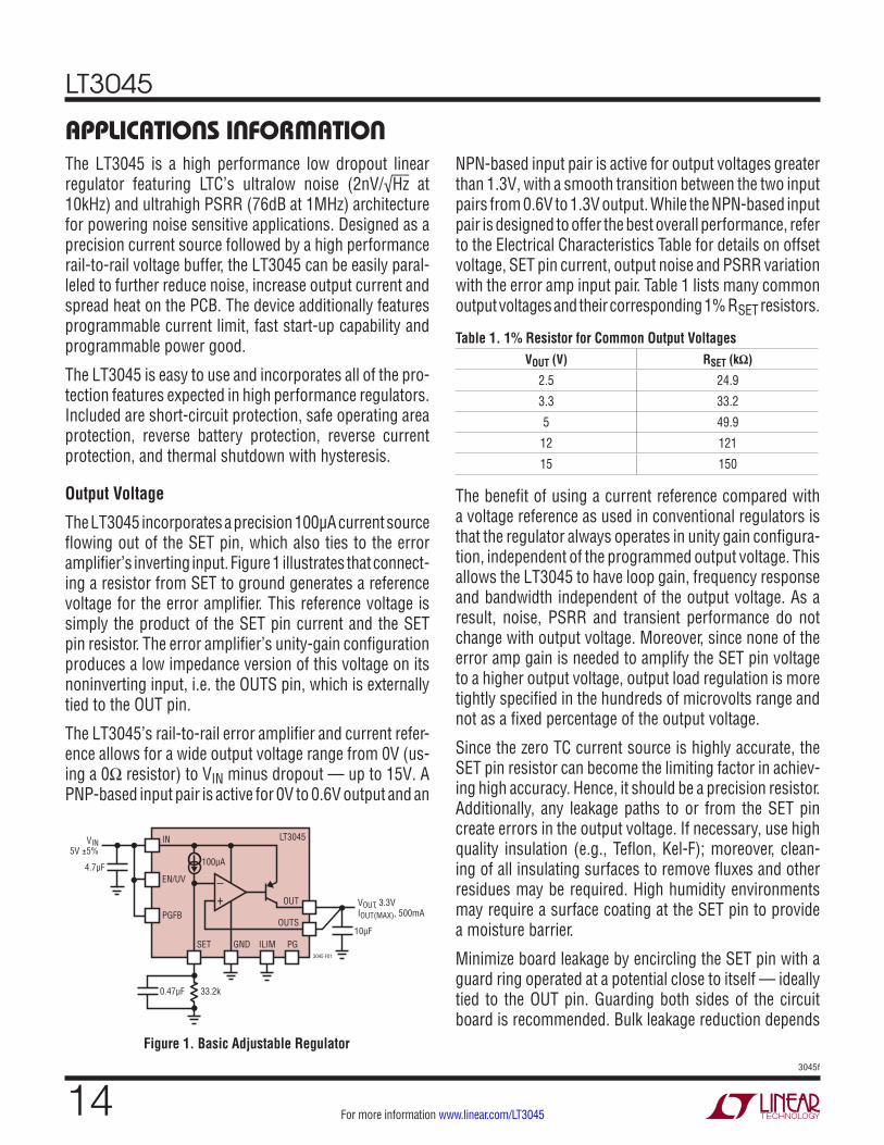
applicaTions inForMaTionThe LT3045 is a high performance low dropout linear regulator featuring LTC’s ultralow noise (2nV/√Hz at 10kHz) and ultrahigh PSRR (76dB at 1MHz) architecture for powering noise sensitive applications. Designed as a precision current source followed by a high performance rail-to-rail voltage buffer, the LT3045 can be easily paral-leled to further reduce noise, increase output current and spread heat on the PCB. The device additionally features programmable current limit, fast start-up capability and programmable power good.
The LT3045 is easy to use and incorporates all of the pro-tection features expected in high performance regulators. Included are short-circuit protection, safe operating area protection, reverse battery protection, reverse current protection, and thermal shutdown with hysteresis.
Output Voltage
The LT3045 incorporates a precision 100µA current source flowing out of the SET pin, which also ties to the error amplifier’s inverting input. Figure 1 illustrates that connect-ing a resistor from SET to ground generates a reference voltage for the error amplifier. This reference voltage is simply the product of the SET pin current and the SET pin resistor. The error amplifier’s unity-gain configuration produces a low impedance version of this voltage on its noninverting input, i.e. the OUTS pin, which is externally tied to the OUT pin.
The LT3045’s rail-to-rail error amplifier and current refer-ence allows for a wide output voltage range from 0V (us-ing a 0Ω resistor) to VIN minus dropout — up to 15V. A PNP-based input pair is active for 0V to 0.6V output and an
NPN-based input pair is active for output voltages greater than 1.3V, with a smooth transition between the two input pairs from 0.6V to 1.3V output. While the NPN-based input pair is designed to offer the best overall performance, refer to the Electrical Characteristics Table for details on offset voltage, SET pin current, output noise and PSRR variation with the error amp input pair. Table 1 lists many common output voltages and their corresponding 1% RSET resistors.
Table 1. 1% Resistor for Common Output VoltagesVOUT (V) RSET (kΩ)
2.5 24.9
3.3 33.2
5 49.9
12 121
15 150
The benefit of using a current reference compared with a voltage reference as used in conventional regulators is that the regulator always operates in unity gain configura-tion, independent of the programmed output voltage. This allows the LT3045 to have loop gain, frequency response and bandwidth independent of the output voltage. As a result, noise, PSRR and transient performance do not change with output voltage. Moreover, since none of the error amp gain is needed to amplify the SET pin voltage to a higher output voltage, output load regulation is more tightly specified in the hundreds of microvolts range and not as a fixed percentage of the output voltage.
Since the zero TC current source is highly accurate, the SET pin resistor can become the limiting factor in achiev-ing high accuracy. Hence, it should be a precision resistor. Additionally, any leakage paths to or from the SET pin create errors in the output voltage. If necessary, use high quality insulation (e.g., Teflon, Kel-F); moreover, clean-ing of all insulating surfaces to remove fluxes and other residues may be required. High humidity environments may require a surface coating at the SET pin to provide a moisture barrier.
Minimize board leakage by encircling the SET pin with a guard ring operated at a potential close to itself — ideally tied to the OUT pin. Guarding both sides of the circuit board is recommended. Bulk leakage reduction depends
+–
100µA
IN
EN/UV
PGFB
GND
OUT
LT3045
ILIM PG10µF
4.7µF
VIN5V ±5%
0.47µF
VOUT, 3.3VIOUT(MAX), 500mA
3045 F01
33.2k
SET
OUTS
Figure 1. Basic Adjustable Regulator
LT3045
153045f
For more information www.linear.com/LT3045
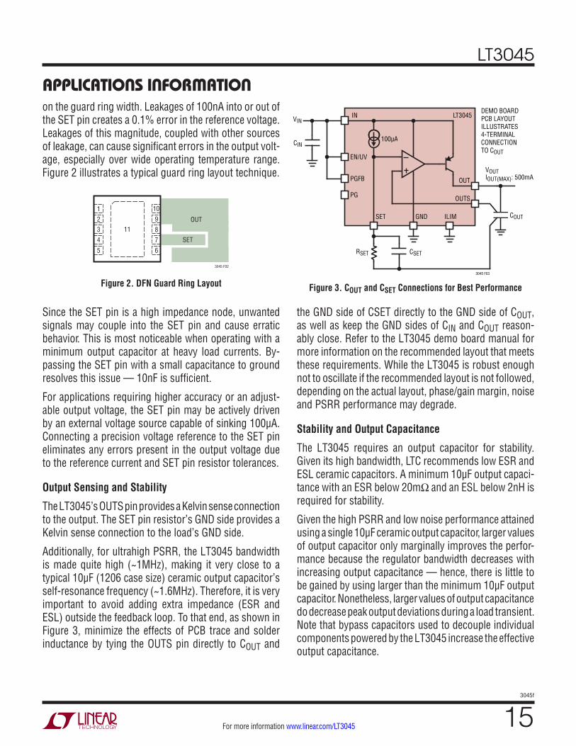
applicaTions inForMaTionon the guard ring width. Leakages of 100nA into or out of the SET pin creates a 0.1% error in the reference voltage. Leakages of this magnitude, coupled with other sources of leakage, can cause significant errors in the output volt-age, especially over wide operating temperature range. Figure 2 illustrates a typical guard ring layout technique.
the GND side of CSET directly to the GND side of COUT, as well as keep the GND sides of CIN and COUT reason-ably close. Refer to the LT3045 demo board manual for more information on the recommended layout that meets these requirements. While the LT3045 is robust enough not to oscillate if the recommended layout is not followed, depending on the actual layout, phase/gain margin, noise and PSRR performance may degrade.
Stability and Output Capacitance
The LT3045 requires an output capacitor for stability. Given its high bandwidth, LTC recommends low ESR and ESL ceramic capacitors. A minimum 10µF output capaci-tance with an ESR below 20mΩ and an ESL below 2nH is required for stability.
Given the high PSRR and low noise performance attained using a single 10µF ceramic output capacitor, larger values of output capacitor only marginally improves the perfor-mance because the regulator bandwidth decreases with increasing output capacitance — hence, there is little to be gained by using larger than the minimum 10µF output capacitor. Nonetheless, larger values of output capacitance do decrease peak output deviations during a load transient. Note that bypass capacitors used to decouple individual components powered by the LT3045 increase the effective output capacitance.
3045 F02
11OUT
SET
10
9
6
7
8
4
5
3
2
1
Figure 2. DFN Guard Ring Layout Figure 3. COUT and CSET Connections for Best Performance
Since the SET pin is a high impedance node, unwanted signals may couple into the SET pin and cause erratic behavior. This is most noticeable when operating with a minimum output capacitor at heavy load currents. By-passing the SET pin with a small capacitance to ground resolves this issue — 10nF is sufficient.
For applications requiring higher accuracy or an adjust-able output voltage, the SET pin may be actively driven by an external voltage source capable of sinking 100µA. Connecting a precision voltage reference to the SET pin eliminates any errors present in the output voltage due to the reference current and SET pin resistor tolerances.
Output Sensing and Stability
The LT3045’s OUTS pin provides a Kelvin sense connection to the output. The SET pin resistor’s GND side provides a Kelvin sense connection to the load’s GND side.
Additionally, for ultrahigh PSRR, the LT3045 bandwidth is made quite high (~1MHz), making it very close to a typical 10µF (1206 case size) ceramic output capacitor’s self-resonance frequency (~1.6MHz). Therefore, it is very important to avoid adding extra impedance (ESR and ESL) outside the feedback loop. To that end, as shown in Figure 3, minimize the effects of PCB trace and solder inductance by tying the OUTS pin directly to COUT and
COUT
RSET CSET
CIN
OUT
IN
SET
LT3045DEMO BOARD PCB LAYOUT ILLUSTRATES 4-TERMINALCONNECTION TO COUT
100µA
OUTSPG
ILIM
3045 F03
GND
PGFB
EN/UV
VOUTIOUT(MAX): 500mA
VIN

LT3045
163045f
For more information www.linear.com/LT3045
applicaTions inForMaTionGive extra consideration to the type of ceramic capacitors used. They are manufactured with a variety of dielectrics, each with different behavior across temperature and applied voltage. The most common dielectrics used are specified with EIA temperature characteristic codes of Z5U, Y5V, X5R and X7R. The Z5U and Y5V dielectrics are good for providing high capacitance in the small packages, but they tend to have stronger voltage and temperature coefficients as shown in Figure 4 and Figure 5. When used with a 5V regulator, a 16V 10µF Y5V capacitor can exhibit an effective value as low as 1µF to 2µF for the DC bias voltage applied over the operating temperature range.
X5R and X7R dielectrics result in more stable character-istics and are thus more suitable for LT3045. The X7R dielectric has better stability across temperature, while the X5R is less expensive and is available in higher values. Nonetheless, care must still be exercised when using X5R and X7R capacitors. The X5R and X7R codes only specify operating temperature range and the maximum capacitance change over temperature. While capacitance change due to DC bias for X5R and X7R is better than Y5V and Z5U dielectrics, it can still be significant enough to drop capacitance below sufficient levels. As shown in Figure 6, capacitor DC bias characteristics tend to improve as component case size increases, but verification of expected capacitance at the operating voltage is highly recommended. Due to its good voltage coefficient in small case sizes, LTC recommends using Murata’s GJ8 series ceramic capacitors.
High Vibration Environments
Voltage and temperature coefficients are not the only sources of problems. Some ceramic capacitors have a piezoelectric response. A piezoelectric device generates voltage across its terminals due to mechanical stress upon it, similar to how a piezoelectric microphone works. For a ceramic capacitor, this stress can be induced by mechanical vibrations within the system or due to thermal transients.
LT3045 applications in high vibration environments have three distinct piezoelectric noise generators: ceramic output, input, and SET pin capacitors. However, due to LT3045’s very low output impedance over a wide fre-quency range, negligible output noise is generated using
Figure 4. Ceramic Capacitor DC Bias Characteristics
Figure 5. Ceramic Capacitor Temperature Characteristics
Figure 6. Capacitor Voltage Coefficient for Different Case Sizes
DC BIAS VOLTAGE (V)
BOTH CAPACITORS ARE 16V,1210 CASE SIZE, 10µF
0–100
CHAN
GE IN
VAL
UE (%
)
–80
642 8 10 12
3045 F04
14
0
20
–60
–40
X5R
Y5V
–20
16
TEMPERATURE (°C)–50
–100
CHAN
GE IN
VAL
UE (%
)
–80
250–25 50 75 100
3045 F05
0
20
40
–60
–40 Y5V
–20
125
BOTH CAPACITORS ARE 16V,1210 CASE SIZE, 10µF
X5R
DC BIAS (V)1
–100
CHAN
GE IN
VAL
UE (%
)
–80
–60
–40
–20
0
20
5 10 15 20
3045 F06
25
GRM SERIES, 0805, 1.45mm THICKGRM SERIES, 1206, 1.8mm THICKGRM SERIES, 1210, 2.2mm THICKGJ8 SERIES, 1206, 1.9mm THICK
MURATA: 25V,10%, X7R/X5R, 10µF CERAMIC

LT3045
173045f
For more information www.linear.com/LT3045
applicaTions inForMaTiona ceramic output capacitor. Similarly, due to LT3045’s ultrahigh PSRR, negligible output noise is generated using a ceramic input capacitor. Nonetheless, given the high SET pin impedance, any piezoelectric response from a ceramic SET pin capacitor generates significant output noise – peak-to-peak excursions of hundreds of µVs. However, due to the SET pin capacitor’s high ESR and ESL tolerance, any non-piezoelectrically responsive (tantalum, electrolytic, or film) capacitor can be used at the SET pin – although electrolytic capacitors tend to have high 1/f noise. In any case, use of surface mount capacitor is highly recommended.
Stability and Input Capacitance
The LT3045 is stable with a minimum 4.7µF IN pin capacitor. LTC recommends using low ESR ceramic capacitors. In cases where long wires connect the power supply to the LT3045’s input and ground terminals, the use of low value input capacitors combined with a large load current can result in instability. The resonant LC tank circuit formed by the wire inductance and the input capacitor is the cause and not because of LT3045’s instability.
The self-inductance, or isolated inductance, of a wire is directly proportional to its length. The wire diameter, however, has less influence on its self-inductance. For example, the self-inductance of a 2-AWG isolated wire with a diameter of 0.26" is about half the inductance of a 30-AWG wire with a diameter of 0.01". One foot of 30-AWG wire has 465nH of self-inductance.
Several methods exist to reduce a wire’s self-inductance. One method divides the current flowing towards the LT3045 between two parallel conductors. In this case, placing the wires further apart reduces the inductance; up to a 50% reduction when placed only a few inches apart. Splitting the wires connect two equal inductors in parallel. However, when placed in close proximity to each other, their mu-tual inductance adds to the overall self inductance of the wires — therefore a 50% reduction is not possible in such cases. The second and more effective technique to reduce the overall inductance is to place the forward and return current conductors (the input and ground wires) in close proximity. Two 30-AWG wires separated by 0.02" reduce the overall inductance to about one-fifth of a single wire.
If a battery mounted in close proximity powers the LT3045, a 4.7µF input capacitor suffices for stability. However, if a distantly located supply powers the LT3045, use a larger value input capacitor. Use a rough guideline of 1µF (in addition to the 4.7µF minimum) per 6" of wire length. The minimum input capacitance needed to stabilize the application also varies with the output capacitance as well as the load current. Placing additional capacitance on the LT3045’s output helps. However, this requires significantly more capacitance compared to additional input bypassing. Series resistance between the supply and the LT3045 input also helps stabilize the application; as little as 0.1Ω to 0.5Ω suffices. This impedance dampens the LC tank circuit at the expense of dropout voltage. A better alternative is to use a higher ESR tantalum or electrolytic capacitor at the LT3045 input in parallel with a 4.7µF ceramic capacitor.
PSRR and Input Capacitance
For applications utilizing the LT3045 for post-regulating switching converters, placing a capacitor directly at the LT3045 input results in ac current (at the switching frequency) to flow near the LT3045. This relatively high-frequency switching current generates a magnetic field that couples to the LT3045 output, thereby degrading its effective PSRR. While highly dependent on the PCB, the switching pre-regulator, the input capacitance, amongst other factors, the PSRR degradation can be easily over 30dB at 1MHz. This degradation is present even if the LT3045 is de-soldered from the board, because it ef-fectively degrades the PSRR of the PC board itself. While negligible for conventional low PSRR LDOs, LT3045’s ultrahigh PSRR requires careful attention to higher order parasitics in order to extract the full performance offered by the regulator.
To mitigate the flow of high-frequency switching current near the LT3045, the LT3045 input capacitor can be entirely removed -- as long as the switching converter’s output capacitor is located more than an inch away from the LT3045. Magnetic coupling rapidly decreases with increas-ing distance. Nonetheless, if the switching pre-regulator is placed too far away (conservatively more than a couple inches) from the LT3045, with no input capacitor present, as with any regulator, the LT3045 input will oscillate at the

LT3045
183045f
For more information www.linear.com/LT3045
applicaTions inForMaTionparasitic LC resonance frequency. Besides, it is generally a very common (and a preferred) practice to bypass regula-tor input with some capacitance. So this option is fairly limited in its scope and not the most palatable solution.
To that end, LTC recommends using the LT3045 demo board layout for achieving the best possible PSRR perfor-mance. The LT3045 demo board layout utilizes magnetic field cancellation techniques to prevent PSRR degradation caused by this high-frequency current flow—while utilizing the input capacitor.
Filtering High Frequency Spikes
For applications where the LT3045 is used to post-regulate a switching converter, its high PSRR effectively sup-presses any “noise” present at the switcher’s switching frequency — typically 100kHz to 4MHz. However, the very high frequency (hundreds of MHz) “spikes” — beyond the LT3045’s bandwidth — associated with the switcher’s power switch transition times will almost directly pass through the LT3045. While the output capacitor is partly intended to absorb these spikes, its ESL will limit its ability at these frequencies. A ferrite bead or even the inductance associated with a short (e.g. 0.5”) PCB trace between the switcher’s output and the LT3045’s input can serve as an LC-filter to suppress these very high frequency spikes.
Output Noise
The LT3045 offers many advantages with respect to noise performance. Traditional linear regulators have several sources of noise. The most critical noise sources for a traditional regulator are its voltage reference, error amplifier, noise from the resistor divider network used for setting output voltage and the noise gain created by this resistor divider. Many low noise regulators pin out their voltage reference to allow for noise reduction by bypassing the reference voltage.
Unlike most linear regulators, the LT3045 does not use a voltage reference; instead, it uses a 100µA current refer-ence. The current reference operates with typical noise current level of 20pA/√Hz (6nARMS over a 10Hz to 100kHz bandwidth). The resultant voltage noise equals the current noise multiplied by the resistor value, which in turn is RMS summed with the error amplifier’s noise and the resistor’s
own noise of √4kTR — whereby k = Boltzmann’s constant 1.38 • 10–23J/K and T is the absolute temperature.
One problem that conventional linear regulators face is that the resistor divider setting the output voltage gains up the reference noise. In contrast, the LT3045’s unity-gain follower architecture presents no gain from the SET pin to the output. Therefore, if a capacitor bypasses the SET pin resistor, then the output noise is independent of the programmed output voltage. The resultant output noise is then set just by the error amplifier’s noise — typically 2nV/√Hz from 10kHz to 1MHz and 0.8µVRMS in a 10Hz to 100kHz bandwidth using a 4.7µF SET pin capacitor. Paral-leling multiple LT3045s further reduces noise by √N, for N parallel regulators.
Refer to the Typical Performance Characteristics section for noise spectral density and RMS integrated noise over various load currents and SET pin capacitances.
Set Pin (Bypass) Capacitance: Noise, PSRR, Transient Response and Soft-Start
In addition to reducing output noise, using a SET pin bypass capacitor also improves PSRR and transient performance. Note that any bypass capacitor leakage deteriorates the LT3045’s DC regulation. Capacitor leakage of even 100nA is a 0.1% DC error. Therefore, LTC recommends the use of a good quality low leakage ceramic capacitor.
Using a SET pin bypass capacitor also soft-starts the output and limits inrush current. The RC time constant, formed by the SET pin resistor and capacitor, controls soft-start time. Ramp-up rate from 0 to 90% of nominal VOUT is:
tSS ≈ 2.3 • RSET • CSET (Fast Start-Up Disabled)
Fast Start-Up
For ultralow noise applications that require low 1/f noise (i.e. at frequencies below 100Hz), a larger value SET pin capacitor is required, up to 22µF. While this would normally significantly increase the regulator’s start-up time, the LT3045 incorporates fast start-up circuitry that increases the SET pin current to about 2mA during start-up.
As shown in the Block Diagram, the 2mA current source remains engaged while PGFB is below 300mV, unless the

LT3045
193045f
For more information www.linear.com/LT3045
applicaTions inForMaTionregulator is in current limit, dropout, thermal shutdown or input voltage is below minimum VIN.
If fast start-up capability is not used, tie PGFB to IN or to OUT for output voltages above 300mV. Note that doing so also disables power good functionality.
ENABLE/UVLO
The EN/UV pin is used to put the regulator into a mi-cropower shutdown state. The LT3045 has an accurate 1.24V turn-on threshold on the EN/UV pin with 130mV of hysteresis. This threshold can be used in conjunction with a resistor divider from the input supply to define an accurate undervoltage lockout (UVLO) threshold for the regulator. The EN/UV pin current (IEN) at the threshold from the Electrical Characteristics table needs to be considered when calculating the resistor divider network:
VIN(UVLO) =1.24V • 1+
REN2REN1
⎛
⎝⎜
⎞
⎠⎟+IEN •REN2
The EN/UV pin current (IEN) can be ignored if REN1 is less than 100k. If unused, tie EN/UV pin to IN.
Programmable Power Good
As illustrated in the Block Diagram, power good thresh-old is user programmable using the ratio of two external resistors, RPG2 and RPG1:
VOUT(PG _ THRESHOLD) =0.3V • 1+
RPG2RPG1
⎛
⎝⎜
⎞
⎠⎟+IPGFB •RPG2
If the PGFB pin increases above 300mV, the open-collector PG pin de-asserts and becomes high impedance. The power good comparator has 7mV hysteresis and 5µs of deglitching. The PGFB pin current (IPGFB) from the Electrical Characteristics table must be considered when determining the resistor divider network. The PGFB pin current (IPGFB) can be ignored if RPG1 is less than 30k. If power good functionality is not used, float the PG pin. Please note that programmable power good and fast start-up capabilities are disabled for output voltages below 300mV.
Externally Programmable Current Limit
The ILIM pin’s current limit threshold is 300mV. Connecting a resistor from ILIM to GND sets the maximum current flowing out of the ILIM pin, which in turn programs the LT3045’s current limit. With a 150mA • kΩ programming scale factor, the current limit can be calculated as follows:
Current Limit =
150mA •kΩRILIM
For example, a 1kΩ resistor programs the current limit to 150mA and a 2kΩ resistor programs the current limit to 75mA. For good accuracy, Kelvin connect this resistor to the LT3045’s GND pin.
In cases where IN-to-OUT differential is greater than 12V, the LT3045’s foldback circuitry decreases the internal current limit. As a result, internal current limit may over-ride the externally programmed current limit level to keep the LT3045 within its safe-operating-area (SOA). See the Internal Current Limit vs Input-to-Output Differential graph in the Typical Performance Characteristics section.
As shown in the Block Diagram, the ILIM pin sources current proportional (1:500) to output current; therefore, it also serves as a current monitoring pin with a 0V to 300mV range. If external current limit or current monitoring is not used, tie ILIM to GND.
Output Overshoot Recovery
During a load step from full load to no load (or light load), the output voltage overshoots before the regulator responds to turn the power transistor OFF. Given that there is no load (or very light load) present at the output, it takes a long time to discharge the output capacitor.
As illustrated in the Block Diagram, the LT3045 incorporates an overshoot recovery circuitry that turns on a current sink to discharge the output capacitor in the event OUTS is higher than SET. This current is typically about 4mA. No load recovery is disabled for input voltages less than 2.5V or output voltages less than 1.5V.
LT3045
203045f
For more information www.linear.com/LT3045
applicaTions inForMaTionIf OUTS is externally held above SET, the current sink turns ON in an attempt to restore OUTS to its programmed voltage. The current sink remains ON until the external circuitry releases OUTS.
Direct Paralleling for Higher Current
Higher output current is obtained by paralleling multiple LT3045s. Tie all SET pins together and all IN pins together. Connect the OUT pins together using small pieces of PCB trace (used as a ballast resistor) to equalize currents in the LT3045s. PCB trace resistance in milliohms/inch is shown in Table 2.
Table 2. PC Board Trace Resistance WEIGHT (oz) 10mil WIDTH 20mil WIDTH
1 54.3 27.1
2 27.1 13.6
Trace resistance is measured in mΩ/in.
The small worst-case offset of 2mV for each paralleled LT3045 minimizes the required ballast resistor value. Figure 7 illustrates that two LT3045s, each using a 20mΩ PCB trace ballast resistor, provide better than 20% accurate output current sharing at full load. The two 20mΩ external resistors only add 10mV of output regulation drop with a 1A maximum current. With a 3.3V output, this only adds 0.3% to the regulation accuracy. As has been discussed previously, tie the OUTS pin directly to the output capacitor.
More than two LT3045s can also be paralleled for even higher output current and lower output noise. Paralleling multiple LT3045s is also useful for distributing heat on the PCB. For applications with high input-to-output voltage differential, an input series resistor or resistor in parallel with the LT3045 can also be used to spread heat.
PCB Layout Considerations
Given the LT3045’s high bandwidth and ultrahigh PSRR, careful PCB layout must be employed to achieve full device performance. Figure 8 shows a recommended layout that delivers full performance of the regulator. Refer to the LT3045’s DC2491A demo board manual for further details.
Figure 8. Recommended DFN Layout
+–
100µA
IN
EN/UV
PGFB
GND
OUT
LT3045
ILIM PG 10µF
20mΩ
VOUT3.3VIOUT(MAX)1A
3045 F07
16.5k
SET
OUTS
+–
100µA
IN
EN/UV
PGFB
GND
OUT
LT3045
ILIM PG 10µF
20mΩ
10µF
VIN5V ±5%
SET
OUTS
0.47µF
Figure 7. Parallel Devices

LT3045
213045f
For more information www.linear.com/LT3045
Thermal Considerations
The LT3045 has internal power and thermal limiting cir-cuits that protect the device under overload conditions. The thermal shutdown temperature is nominally 165°C with about 8°C of hysteresis. For continuous normal load conditions, do not exceed the maximum junction temperature (125°C for E- and I-grades). It is important to consider all sources of thermal resistance from junction to ambient. This includes junction-to-case, case-to-heat sink interface, heat sink resistance or circuit board-to-ambient as the application dictates. Additionally, consider all heat sources in close proximity to the LT3045.
The undersides of the DFN and MSOP packages have exposed metal from the lead frame to the die attachment. Both packages allow heat to directly transfer from the die junction to the PCB metal to limit maximum operating junction temperature. The dual-in-line pin arrangement allows metal to extend beyond the ends of the package on the topside (component side) of the PCB.
For surface mount devices, heat sinking is accomplished by using the heat spreading capabilities of the PCB and its copper traces. Copper board stiffeners and plated through-holes can also be used to spread the heat generated by the regulator.
Tables 3 and 4 list thermal resistance as a function of copper area on a fixed board size. All measurements were taken in still air on a 4 layer FR-4 board with 1oz solid internal planes and 2oz top/bottom planes with a total board thick-ness of 1.6mm. The four layers were electrically isolated with no thermal vias present. PCB layers, copper weight, board layout and thermal vias affect the resultant thermal resistance. For more information on thermal resistance and high thermal conductivity test boards, refer to JEDEC standard JESD51, notably JESD51-7 and JESD51-12. Achieving low thermal resistance necessitates attention to detail and careful PCB layout.
Table 3. Measured Thermal Resistance for DFN PackageCOPPER AREA
BOARD AREATHERMAL
RESISTANCETOP SIDE* BOTTOM SIDE
2500mm2 2500mm2 2500mm2 34°C/W
1000mm2 2500mm2 2500mm2 34°C/W
225mm2 2500mm2 2500mm2 35°C/W
100mm2 2500mm2 2500mm2 36°C/W
*Device is mounted on topside
Table 4. Measured Thermal Resistance for MSOP PackageCOPPER AREA
BOARD AREATHERMAL
RESISTANCETOP SIDE* BOTTOM SIDE
2500mm2 2500mm2 2500mm2 33°C/W
1000mm2 2500mm2 2500mm2 33°C/W
225mm2 2500mm2 2500mm2 34°C/W
100mm2 2500mm2 2500mm2 35°C/W
*Device is mounted on topside
Calculating Junction Temperature
Example: Given an output voltage of 3.3V and input voltage of 5V ± 5%, output current range from 1mA to 500mA, and a maximum ambient temperature of 85°C, what is the maximum junction temperature?
The LT3045’s power dissipation is:
IOUT(MAX) • (VIN(MAX) – VOUT) + IGND • VIN(MAX)
where:
IOUT(MAX) = 500mA
VIN(MAX) = 5.25V
IGND (at IOUT = 500mA and VIN = 5.25V) = 12.5mA
thus:
PDISS = 0.5A • (5.25V – 3.3V) + 12.5mA • 5.25V = 1W
Using a DFN package, the thermal resistance is in the range of 34°C/W to 36°C/W depending on the copper area. Therefore, the junction temperature rise above ambient approximately equals:
1W • 35°C/W = 35°C
The maximum junction temperature equals the maxi-mum ambient temperature plus the maximum junction temperature rise above ambient:
TJMAX = 85°C + 35°C = 120°C
applicaTions inForMaTion

LT3045
223045f
For more information www.linear.com/LT3045
Typical applicaTionsOverload Recovery
Like many IC power regulators, the LT3045 incorporates safe-operating-area (SOA) protection. The SOA protection activates at input-to-output differential voltages greater than 12V. The SOA protection decreases the current limit as the input-to-output differential increases and keeps the power transistor inside a safe operating region for all values of input-to-output voltages up to the LT3045’s absolute maximum ratings. The LT3045 provides some level of output current for all values of input-to-output dif-ferentials. Refer to the Current Limit curves in the Typical Performance Characteristics section. When power is first applied and input voltage rises, the output follows the input and keeps the input-to-output differential low to allow the regulator to supply large output current and start-up into high current loads.
Due to current limit foldback, however, at high input volt-ages a problem can occur if the output voltage is low and the load current is high. Such situations occur after the removal of a short-circuit or if the EN/UV pin is pulled high after the input voltage has already turned ON. The load line in such cases intersects the output current profile at two points. The regulator now has two stable operating points. With this double intersection, the input power supply may need to be cycled down to zero and brought back up again to make the output recover. Other linear regulators with foldback current limit protection (such as the LT1965 and LT1963A) also exhibit this phenomenon, so it is not unique to the LT3045.
Protection Features
The LT3045 incorporates several protection features for battery-powered applications. Precision current limit and thermal overload protection protect the LT3045 against overload and fault conditions at the device’s output. For normal operation, do not allow the junction temperature to exceed 125°C (E-grade, I-grade).
To protect the LT3045’s low noise error amplifier, the SET-to-OUTS protection clamp limits the maximum voltage between SET and OUTS with a maximum DC current of 20mA through the clamp. So for applications where SET is actively driven by a voltage source, the voltage source must be current limited to 20mA or less. Moreover, to limit the transient current flowing through these clamps during a transient fault condition, limit the maximum value of the SET pin capacitor (CSET) to 22µF.
The LT3045 also incorporates reverse input protection whereby the IN pin withstands reverse voltages of up to –20V without causing any input current flow and without developing negative voltages at the OUT pin. The regulator protects both itself and the load against batteries that are plugged-in backwards.
In circuits where a backup battery is required, several different input/output conditions can occur. The output voltage may be held up while the input is either pulled to GND, pulled to some intermediate voltage, or left open-circuit. In all of these cases, the reverse current protection circuitry prevents current flow from output to the input. Nonetheless, due to the OUTS-to-SET clamp, unless the SET pin is floating, current can flow to GND through the SET pin resistor as well as up to 15mA to GND through the output overshoot recovery circuitry. This current flow through the output overshoot recovery circuitry can be significantly reduced by placing a Schottky diode between OUTS and SET pins, with its anode at the OUTS pin.

LT3045
233045f
For more information www.linear.com/LT3045
Typical applicaTions
12VIN to 3.3VOUT with 0.8µVRMS Integrated Noise
100µA
IN
EN/UV
PG
GND
OUT
LT3045
ILIM PGFB453k
10µF
4.7µF
VIN12V ±5%
200k
4.7µF
VOUT3.3VIOUT200mA
49.9k
3045 TA02
33.2k
SET
OUTS
+–
750Ω
Low Noise CC/CV Lab Power Supply Ultralow Noise Current Source for RF Biasing Applications
10µF
3045 TA04
4.7µF
OUTPUT CURRENT NOISE = 0.8µVRMS/ROUTINCREASE R1 (AND RSET) TO REDUCE CURRENT NOISE
4.7µF
RSET2k
RLOAD
VIN1.8V to 20V
OUT
IN
SET
LT3045
VOUT(MAX): 15VIOUT: 200mA
100µA
OUTSPGILIMGND
PGFB
EN/UV
ROUT = R1 + RLOAD
R11Ω
10µF
0.47µF
4.7µF
RSETRIOUT
VIN
OUT
IN
SET
LT3045
VOUT
100µA
OUTS
PGFB
ILIMGND
PG
EN/UV
3045 TA03
+–
VOUT(MAX) = 100μA • RSET
IOUT(MAX) = 150mA • kΩRIOUT

LT3045
243045f
For more information www.linear.com/LT3045
Typical applicaTions
Programming Undervoltage Lockout
10µF
33.2k0.47µF
REN2110k
REN149.9k
4.7µF
VIN4V Turn-ON
3.4V Turn-OFF
OUT
IN
SET
LT3045
VOUT3.3VIOUT(MAX)500mA
100µA
OUTSEN/UV
ILIMGND
PG
PGFB
3045 TA05
+–
VIN(UVLO)RISING =1.24V • 1+ 110k
49.9k⎛
⎝⎜
⎞
⎠⎟
Ratiometric Tracking
10µF
0.1µF
10µF
33.2k
10µF
0.1µF 16.9k
VIN5.5V TO 20V
OUT
IN
SET
LT3045
VOUT3.3VMIN LOAD 200µA
100µA
OUTS
PGFB
ILIMGND
PG
EN/UV
OUT
IN
SET
LT3045
VOUT5V
100µA
OUTS
PGFB
ILIMGND
PG
EN/UV
3045 TA06
+–

LT3045
253045f
For more information www.linear.com/LT3045
Typical applicaTions
Paralleling Multiple Devices Using ILIM (Current Monitor) to Cancel Ballast Resistor Drop
Ultralow 1/f Noise Reference Buffer
10µF
4.7µF
4.7µF
OUT
IN
SET
LT3045
VOUT = 5VIOUT(MAX)500mA
100µA
OUTS
PGFB
ILIMGND
PG
EN/UV
LTC6655-5
3045 TA07
+–
1,2
3,4,5
6,7
10µF 49.9k
1k
VIN6V ±5%
10µF
N = NUMBER OF DEVICES IN PARALLELRCDC = CABLE (BALLAST RESISTOR) DROP CANCELLATION RESISTORRILIM = CURRENT LIMIT PROGRAMMING RESISTORRBALLAST = BALLAST RESISTORILIM = OUTPUT CURRENT LIMIT
10µF
20mΩ
1µF
10µF
OUT
IN
SET
LT3045
100µA 100µA
OUTS
PGFB
ILIMGND
PG
EN/UV
IN
PGFB
PG
EN/UV+–
16.5k
RILIM287Ω
RCDC5Ω
RILIM = 150mA • kΩ/ILIM – RCDC • N = 287Ω (FOR 500mA ILIM PER REGULATOR)
RCDC = RBALLAST • 500/N = 5Ω
VOUT = 3.3VIOUT(MAX) = 1A
287Ω
20mΩ
+–
3045 TA08
OUT
LT3045
OUTS
SETILIM GND
VIN5V ±5%

LT3045
263045f
For more information www.linear.com/LT3045
Typical applicaTions
Paralleling Multiple LT3045s for 2A Output Current
10µF 10µF
20mΩ
4.7µF
OUT
IN
SET
LT3045
100µA 100µA
OUTS
PGFB
ILIMGND
PG
EN/UV
IN
PGFB
PG
EN/UV+–
8.25k
20mΩ
+–
3045 TA09
OUT
LT3045
OUTS
SETILIM GND
10µF 10µF
20mΩ
22µF
OUT
IN
SET
LT3045
100µA 100µA
OUTS
PGFBGND
PG
EN/UV
IN
PGFB
PG
EN/UV+–
453k
200k
49.9k VOUT = 3.3VIOUT(MAX) = 2ADROPOUT = 300mV
20mΩ
+–
OUT
LT3045
OUTS
SETILIMILIM GND
OUTPUT NOISE = 0.8µVRMS
4= 0.4µVRMS
VIN5V ±5%

LT3045
273045f
For more information www.linear.com/LT3045
Typical applicaTions
Low Noise Wheatstone Bridge Power Supply
10µF
33.2k4.7µF
200k
453k
49.9k
4.7µF
R2
R1 R3
+ –
R4
VIN5V ±5%
OUT
IN
SET
LT3045
3045 TA10
VOUT: 3.3V AND IOUT(MAX): 500mA
100µA
OUTS
PGFBILIMGND
PG
EN/UV
RESISTORTOLERANCE BRIDGE PSRR NOISE AT VBRIDGE
USING LT1763
1%
5%
40dB
26dB
8nVRMS
42.5nVRMS
PERFECTMATCHING INFINITE –
NOISE AT VBRIDGEUSING LT3045
200nVRMS
1000nVRMS
–
LT1763 NOISE: 20µVRMS (10Hz TO 100kHz)LT3045 NOISE: 0.8µVRMS (10Hz TO 100kHz)
VBRIDGE
+–
PGFB Disabled without Reverse Input Protection PGFB Disabled with Reverse Input Protection
RSET
10µF
0.47µF
4.7µF
VIN
OUT
IN
SET
LT3045
VOUT
100µA
OUTS
PGFB
ILIMGND
PG
EN/UV+–
3045 TA11
0.47µF
10µF
1N4148
4.7µF
RSET
VIN
OUT
IN
SET
LT3045
VOUT
100µA
OUTSPGFB
ILIMGNDPG
EN/UV
3045 TA12
+–

LT3045
283045f
For more information www.linear.com/LT3045
package DescripTionPlease refer to http://www.linear.com/product/LT3045#packaging for the most recent package drawings.
3.00 ±0.10(4 SIDES)
NOTE:1. DRAWING TO BE MADE A JEDEC PACKAGE OUTLINE M0-229 VARIATION OF (WEED-2). CHECK THE LTC WEBSITE DATA SHEET FOR CURRENT STATUS OF VARIATION ASSIGNMENT2. DRAWING NOT TO SCALE3. ALL DIMENSIONS ARE IN MILLIMETERS4. DIMENSIONS OF EXPOSED PAD ON BOTTOM OF PACKAGE DO NOT INCLUDE MOLD FLASH. MOLD FLASH, IF PRESENT, SHALL NOT EXCEED 0.15mm ON ANY SIDE5. EXPOSED PAD SHALL BE SOLDER PLATED6. SHADED AREA IS ONLY A REFERENCE FOR PIN 1 LOCATION ON THE TOP AND BOTTOM OF PACKAGE
0.40 ±0.10
BOTTOM VIEW—EXPOSED PAD
1.65 ±0.10(2 SIDES)
0.75 ±0.05
R = 0.125TYP
2.38 ±0.10(2 SIDES)
15
106
PIN 1TOP MARK
(SEE NOTE 6)
0.200 REF
0.00 – 0.05
(DD) DFN REV C 0310
0.25 ±0.05
2.38 ±0.05(2 SIDES)
RECOMMENDED SOLDER PAD PITCH AND DIMENSIONS
1.65 ±0.05(2 SIDES)2.15 ±0.05
0.50BSC
0.70 ±0.05
3.55 ±0.05
PACKAGEOUTLINE
0.25 ±0.050.50 BSC
DD Package10-Lead Plastic DFN (3mm × 3mm)
(Reference LTC DWG # 05-08-1699 Rev C)
PIN 1 NOTCHR = 0.20 OR0.35 × 45°CHAMFER

LT3045
293045f
For more information www.linear.com/LT3045
Information furnished by Linear Technology Corporation is believed to be accurate and reliable. However, no responsibility is assumed for its use. Linear Technology Corporation makes no representa-tion that the interconnection of its circuits as described herein will not infringe on existing patent rights.
package DescripTionPlease refer to http://www.linear.com/product/LT3045#packaging for the most recent package drawings.
MSOP (MSE12) 0213 REV G
0.53 ±0.152(.021 ±.006)
SEATINGPLANE
0.18(.007)
1.10(.043)MAX
0.22 – 0.38(.009 – .015)
TYP
0.86(.034)REF
0.650(.0256)
BSC
12
12 11 10 9 8 7
7
DETAIL “B”
1 6
NOTE:1. DIMENSIONS IN MILLIMETER/(INCH)2. DRAWING NOT TO SCALE3. DIMENSION DOES NOT INCLUDE MOLD FLASH, PROTRUSIONS OR GATE BURRS. MOLD FLASH, PROTRUSIONS OR GATE BURRS SHALL NOT EXCEED 0.152mm (.006") PER SIDE4. DIMENSION DOES NOT INCLUDE INTERLEAD FLASH OR PROTRUSIONS. INTERLEAD FLASH OR PROTRUSIONS SHALL NOT EXCEED 0.152mm (.006") PER SIDE5. LEAD COPLANARITY (BOTTOM OF LEADS AFTER FORMING) SHALL BE 0.102mm (.004") MAX6. EXPOSED PAD DIMENSION DOES INCLUDE MOLD FLASH. MOLD FLASH ON E-PAD SHALL NOT EXCEED 0.254mm (.010") PER SIDE.
0.254(.010) 0° – 6° TYP
DETAIL “A”
DETAIL “A”
GAUGE PLANE
RECOMMENDED SOLDER PAD LAYOUT
BOTTOM VIEW OFEXPOSED PAD OPTION
2.845 ±0.102(.112 ±.004)2.845 ±0.102
(.112 ±.004)
4.039 ±0.102(.159 ±.004)
(NOTE 3)
1.651 ±0.102(.065 ±.004)
1.651 ±0.102(.065 ±.004)
0.1016 ±0.0508(.004 ±.002)
1 2 3 4 5 6
3.00 ±0.102(.118 ±.004)
(NOTE 4)
0.406 ±0.076(.016 ±.003)
REF
4.90 ±0.152(.193 ±.006)
DETAIL “B”CORNER TAIL IS PART OF
THE LEADFRAME FEATURE.FOR REFERENCE ONLY
NO MEASUREMENT PURPOSE
0.12 REF
0.35REF
5.10(.201)MIN
3.20 – 3.45(.126 – .136)
0.889 ±0.127(.035 ±.005)
0.42 ±0.038(.0165 ±.0015)
TYP
0.65(.0256)
BSC
MSE Package12-Lead Plastic MSOP, Exposed Die Pad
(Reference LTC DWG # 05-08-1666 Rev G)

LT3045
303045f
For more information www.linear.com/LT3045 LINEAR TECHNOLOGY CORPORATION 2016
LT 0916 • PRINTED IN USALinear Technology Corporation1630 McCarthy Blvd., Milpitas, CA 95035-7417(408) 432-1900 FAX: (408) 434-0507 www.linear.com/LT3045
relaTeD parTs
Typical applicaTion
+–
100µA
IN
EN/UV
PGFB
GND
OUT
LT3045
ILIM PG 10µF
20mΩ
VOUT3.3VIOUT(MAX)1A
3045 TA13
16.5k
SET
OUTS
+–
100µA
IN
EN/UV
PGFB
GND
OUT
LT3045
ILIM PG 10µF
20mΩ
10µF
VIN5V ±5%
SET
OUTS
0.47µF
Parallel Devices
PART NUMBER DESCRIPTION COMMENTS
LT1761 100mA, Low Noise LDO 300mV Dropout Voltage, Low Noise: 20µVRMS, VIN = 1.8V to 20V, TSOT-23 Package
LT1763 500mA, Low Noise LDO 300mV Dropout Voltage, Low Noise: 20μVRMS, VIN = 1.8V to 20V, 4mm × 3mm DFN and SO-8 Packages
LT3042 200mA, Ultralow Noise and Ultrahigh PSRR LDO 0.8μVRMS Noise and 79dB PSRR at 1MHz, VIN = 1.8V to 20V, 350mV Dropout Voltage, Programmable Current Limit and Power Good, 3mm × 3mm DFN and MSOP Packages
LT3055 500mA LDO with Diagnostics and Precision Current Limit 340mV Dropout Voltage, Low Noise: 25μVRMS, VIN = 1.8V to 45V, 4mm × 3mm DFN and MSOP Packages
LT3065 500mA Low Noise LDO with Soft-Start 300mV Dropout Voltage, Low Noise: 25μVRMS, VIN = 1.8V to 45V, 3mm × 3mm DFN and MSOP Packages
LT3080 1.1A, Parallelable, Low Noise, Low Dropout Linear Regulator 300mV Dropout Voltage (2-Supply Operation), Low Noise: 40μVRMS, VIN: 1.2V to 36V, VOUT: 0V to 35.7V, Current-Based Reference with 1-Resistor VOUT Set; Directly Parallelable (No Op Amp Required), Stable with Ceramic Capacitors; TO-220, DD-Pak, SOT-223, MSOP and 3mm × 3mm DFN-8 Packages; LT3080-1 Version Has Integrated Internal Ballast Resistor
LT3085 500mA, Parallelable, Low Noise, Low Dropout Linear Regulator
275mV Dropout (2-Supply Operation), Low Noise: 40μVRMS, VIN: 1.2V to 36V, VOUT: 0V to 35.7V, Current-Based Reference with 1-Resistor VOUT Set, Directly Parallelable (No Op Amp Required), Stable with Ceramic Capacitors; MS8E and 2mm × 3mm DFN-6 Packages