Embed Size (px)
Citation preview

Università Degli Studi Di
Padova
Facoltà di Ingegneria
Corso di Laurea: Ingegneria Elettronica
Investigation, Analysis and Design
of a Sub-Bandgap Voltage Reference
for Ultra-Low Voltage Applications
RELATORE
Prof. Bevilacqua Andrea
I CORRELATORE
Ing. Piselli Marco
II CORRELATORE TESI DI LAUREA DI
Ing. Flaibani Marco Zampieri StefanoMatr. N. 586274
Anno Accademico [2011/2012]


To my parents, for all the immense love they have always been giving to me.


Contents
1 Introduction 1
1.1 Voltage Reference Purpose . . . . . . . . . . . . . . . . . . . . 1
1.2 Historical Overview . . . . . . . . . . . . . . . . . . . . . . . . 3
1.3 Temperature Dependence . . . . . . . . . . . . . . . . . . . . . 6
1.3.1 VBE(T ) Derivation . . . . . . . . . . . . . . . . . . . . 6
1.3.2 Discussion on Approximations and Secondary Eects . 12
1.4 Compensation Orders . . . . . . . . . . . . . . . . . . . . . . . 14
1.5 Functional Blocks: Current References . . . . . . . . . . . . . 16
1.5.1 PTAT Current Generator . . . . . . . . . . . . . . . . 16
1.5.2 PTAT 2 Current Reference, Bipolar Implementation . . 18
1.5.3 The Output Stage . . . . . . . . . . . . . . . . . . . . 20
1.6 Impact On a Voltage Regulator Performance . . . . . . . . . . 23
2 Design 29
2.1 The Second Order Curvature-Corrected
Sub-Bandgap . . . . . . . . . . . . . . . . . . . . . . . . . . . 29
2.1.1 Design Overview . . . . . . . . . . . . . . . . . . . . . 32
2.1.2 Performance Overview . . . . . . . . . . . . . . . . . . 35
2.1.3 Performance Evaluation . . . . . . . . . . . . . . . . . 38
2.2 Choosing the Topology . . . . . . . . . . . . . . . . . . . . . . 39
2.3 Preliminary PTAT Stage Analysis . . . . . . . . . . . . . . . . 43
2.4 Errors Compensation Detailed Analysis . . . . . . . . . . . . . 45
2.4.1 Collector Current Mismatch . . . . . . . . . . . . . . . 45
2.4.2 Loop Analysis . . . . . . . . . . . . . . . . . . . . . . . 46
iii

2.4.3 Base Currents . . . . . . . . . . . . . . . . . . . . . . . 47
2.4.4 Mirror Channel Length Modulation and NPN Early
Voltage . . . . . . . . . . . . . . . . . . . . . . . . . . 49
2.4.5 Leakage . . . . . . . . . . . . . . . . . . . . . . . . . . 52
2.5 Diode Loop Topology Design . . . . . . . . . . . . . . . . . . . 58
2.5.1 The PTAT Stage . . . . . . . . . . . . . . . . . . . . . 58
2.5.2 The CTAT and the Non-Linear Stage . . . . . . . . . . 66
2.5.3 The Output Stage . . . . . . . . . . . . . . . . . . . . 71
2.5.4 The Start-up . . . . . . . . . . . . . . . . . . . . . . . 72
2.5.5 PSRR . . . . . . . . . . . . . . . . . . . . . . . . . . . 74
2.5.6 Pseudo-Supply Design . . . . . . . . . . . . . . . . . . 77
2.5.7 AC Stability . . . . . . . . . . . . . . . . . . . . . . . . 79
2.5.8 Monte Carlo . . . . . . . . . . . . . . . . . . . . . . . 96
2.5.9 Extracted Simulation . . . . . . . . . . . . . . . . . . . 102
2.5.10 Performance . . . . . . . . . . . . . . . . . . . . . . . . 104
2.6 Proposed Topology Improvements . . . . . . . . . . . . . . . . 105
3 Measurements Vs Simulations 107
3.1 Analyzed Topologies and Procedures . . . . . . . . . . . . . . 107
3.2 Measurements VS Simulation . . . . . . . . . . . . . . . . . . 111
3.2.1 Voltage Reference and Current Consumption . . . . . . 111
3.2.2 Line Regulation . . . . . . . . . . . . . . . . . . . . . . 113
3.2.3 Leakage . . . . . . . . . . . . . . . . . . . . . . . . . . 113
4 Discussion And Comparison With Other Topologies 117
4.1 Main Objectives . . . . . . . . . . . . . . . . . . . . . . . . . . 117
4.2 Final Comparison and Evaluation . . . . . . . . . . . . . . . . 118
4.2.1 PSRR and Transient Response . . . . . . . . . . . . . . 120
4.2.2 Line Regulation and Start-Up . . . . . . . . . . . . . . 120
4.2.3 Nominal Precision and Statistical Analysis . . . . . . . 121
5 Conclusions 125

A Appendix 127
A.1 Base Emitter Voltage Calculation . . . . . . . . . . . . . . . . 127
A.1.1 General VBE(T ) expression . . . . . . . . . . . . . . . . 127
A.1.2 Precise VBE(T ) calculation . . . . . . . . . . . . . . . . 128
A.2 Linear Regualtor Analysis . . . . . . . . . . . . . . . . . . . . 129
A.2.1 Block Diagram of LDO Linear Regulator . . . . . . . . 129
A.2.2 PTAT W transfer function calculation . . . . . . . . 129
A.3 AC Stability . . . . . . . . . . . . . . . . . . . . . . . . . . . . 130
A.4 Monte Carlo . . . . . . . . . . . . . . . . . . . . . . . . . . . . 132
A.4.1 Resistors Mismatch . . . . . . . . . . . . . . . . . . . . 132
Ringraziamenti 135


List of Figures
1.1 Hilbiber's rst voltage reference: the ancestor. . . . . . . . . . 3
1.2 Widlar's rst bandgap reference. . . . . . . . . . . . . . . . . . 4
1.3 Brokaw's bandgap voltage reference. . . . . . . . . . . . . . . . 5
1.4 Bandgap voltage versus absolute temperature and its rst de-
gree approximation (not to scale). . . . . . . . . . . . . . . . . 9
1.5 N-channel MOSFET, Id over Vgs, temperature as parameter. . 14
1.6 PTAT current generator. . . . . . . . . . . . . . . . . . . . . . 17
1.7 Bipolar PTAT 2 current generator. . . . . . . . . . . . . . . . 19
1.8 PTAT 2 current generator with horizontal NPN placement. . . 19
1.9 Output Stages. . . . . . . . . . . . . . . . . . . . . . . . . . . 21
1.10 Mixed-mode output topology. . . . . . . . . . . . . . . . . . . 23
1.11 LDO linear regulator. . . . . . . . . . . . . . . . . . . . . . . . 24
1.12 Linear voltage regulator block diagram. . . . . . . . . . . . . . 25
1.13 (a)PSRRsystem in function of PSRRBG. (b)PSRRBG. . . . . 28
2.1 Leakage trimmable compensation and PTAT stages. . . . . . 30
2.2 Spt5 sub-Bandgap: CTAT , PTAT 2 and output stages. . . . . 31
2.3 Output stage. . . . . . . . . . . . . . . . . . . . . . . . . . . . 32
2.4 Curvature correction scheme. . . . . . . . . . . . . . . . . . . 33
2.5 Sub-bandgap reference performance. . . . . . . . . . . . . . . 36
2.6 Monte Carlo Vref (T ) spread for three typical temperatures. . . 37
2.7 TC 100% yield for V ref . . . . . . . . . . . . . . . . . . . . . . 38
2.8 Diode Loop topology. . . . . . . . . . . . . . . . . . . . . . . 40
2.9 Diode Loop Bandgap Core V2 (full version). . . . . . . . . . . 42
2.10 The PTAT Stage. . . . . . . . . . . . . . . . . . . . . . . . . 43
vii

2.11 IC over VBE characteristic. . . . . . . . . . . . . . . . . . . . . 45
2.12 PTAT Loop block diagram. . . . . . . . . . . . . . . . . . . . 46
2.13 Early voltage and saturation region approaching eects. . . . . 50
2.14 Early voltage test topology. . . . . . . . . . . . . . . . . . . . 51
2.15 Collector-currents ratio. . . . . . . . . . . . . . . . . . . . . . 51
2.16 Leakage parasitic devices and model. . . . . . . . . . . . . . . 52
2.17 The PTAT Stage. . . . . . . . . . . . . . . . . . . . . . . . . 59
2.18 IB compensation results. . . . . . . . . . . . . . . . . . . . . . 60
2.19 Leakage compensation NPN. . . . . . . . . . . . . . . . . . . . 61
2.20 V PTAT error caused by leakage currents. . . . . . . . . . . . . 63
2.21 PTAT stage, version 3. . . . . . . . . . . . . . . . . . . . . . . 65
2.22 CTAT stage. . . . . . . . . . . . . . . . . . . . . . . . . . . . . 67
2.23 Tuned VS default mirror ratio. . . . . . . . . . . . . . . . . . . 69
2.24 RNL ± 30% span. Balance over Tr eect. . . . . . . . . . . . . 70
2.25 Output Stage, Version 2. . . . . . . . . . . . . . . . . . . . . . 71
2.26 Start-up stage. . . . . . . . . . . . . . . . . . . . . . . . . . . 73
2.27 Pre-regulated pseudo-supply. . . . . . . . . . . . . . . . . . . . 75
2.28 Pre-regulator circuit. . . . . . . . . . . . . . . . . . . . . . . . 77
2.29 Cold current boost. . . . . . . . . . . . . . . . . . . . . . . . 79
2.30 The pseudo-supply PTAT stage, complete representation. . . . 80
2.31 Pseudo-supply AC-loop block diagram. . . . . . . . . . . . . . 82
2.32 No compensation STB analysis. . . . . . . . . . . . . . . . . . 83
2.33 MATLAB verication of poles and zeros placement in the
pseudo-supply: simulator data are dotted. . . . . . . . . . . . 85
2.34 The Bandgap core PTAT stage, complete representation. . . . 86
2.35 MATLAB verication of poles and zeros placement in the
PTAT stage: simulator data are dotted. . . . . . . . . . . . . . 91
2.36 The Bandgap core CTAT stage, complete representation. . . . 92
2.37 MATLAB verication of poles and zeros placement in the
CTAT stage: simulation data are dotted. . . . . . . . . . . . . 95
2.38 Diode loop topology, explicits circuit. . . . . . . . . . . . . . . 96
2.39 Corners on resistors mismatch error. . . . . . . . . . . . . . . 97
2.40 PTAT stage, mirror mismatch. . . . . . . . . . . . . . . . . . . 98

2.41 Current mirror mismatch, PTAT stage contribute. . . . . . . . 99
2.42 Current mirror mismatch, CTAT stage contribute. . . . . . . . 100
2.43 NPN mismatch, PTAT stage contribute. . . . . . . . . . . . . 101
2.44 NPN mismatch, CTAT stage contribute. . . . . . . . . . . . . 101
2.45 Improving steps in layout debug. . . . . . . . . . . . . . . . . 103
3.1 Leakage compensation structure. . . . . . . . . . . . . . . . . 108
3.2 Connections setup for Set 1. . . . . . . . . . . . . . . . . . . 108
3.3 Connections setup for Set 2. . . . . . . . . . . . . . . . . . . 109
3.4 Connections setup for Set 2, inside view. . . . . . . . . . . . 110
3.5 FIB cut: microscope picture. . . . . . . . . . . . . . . . . . . . 110
3.6 VBG measurements VS VBG corner values. . . . . . . . . . . . 111
3.7 Iin measurements VS Iin corner values. . . . . . . . . . . . . . 112
3.8 Output resistance measurement Vs nominal value. . . . . . . . 113
3.9 FIB measurements. . . . . . . . . . . . . . . . . . . . . . . . . 115
3.10 Leakage current: measurements VS simulation. . . . . . . . . . 116
4.1 Performances comparison. . . . . . . . . . . . . . . . . . . . . 119
4.2 Nominal output voltage. . . . . . . . . . . . . . . . . . . . . . 122
4.3 Mixed-mode output stage of Bg3. . . . . . . . . . . . . . . . . 123
A.1 NPN mirror eect, small signal schematic. . . . . . . . . . . . 129
A.2 Small signal circuit for cascoded PTAT stage AC analysis. . . 131


List of Tables
1.1 Blocks table. . . . . . . . . . . . . . . . . . . . . . . . . . . . . 24
2.1 Specications table. . . . . . . . . . . . . . . . . . . . . . . . . 36
2.2 Leakage explanation to Vref variation discussed in 2.4.4. . . . . 57
2.3 Leakage values for VA = −800m. . . . . . . . . . . . . . . . . . 62
2.4 Specications table: Diode-Loop Sub-Bandgap. . . . . . . . . 104
2.5 Improvements table: mixed mode VS diode loop. . . . . . . . 104
2.6 Improvements table: rst VS second design. . . . . . . . . . . 105
3.1 Line regulation estimation. . . . . . . . . . . . . . . . . . . . . 113
3.2 VBG variation between no compensation and FIB2 modication.116
4.1 Analyzed structures. . . . . . . . . . . . . . . . . . . . . . . . 118
4.2 Precision, area and current consumption performance. . . . . . 122
xi

Abstract
The purpose of this thesis is to study and fully comprehend how to realize
a very high performance sub-bandgap (low-voltage) structure. In order to
achieve this result, it was necessary to begin from (and often come back to)
the physics of semiconductor devices before moving to an analog approach
in order to design the voltage reference itself. New formulas, as practical
as accurate, will be derived in order to be able to successfully handle the
many problems one can face during the design of the proposed topology.
Parallel to this design activity, it was possible to study an already developed
sub-bandgap structure, comparing measurements to simulation results and
extracting important evaluations, useful to further improve both the designs.
Layout and extracted simulations have also been taken into account, in order
to assure the best reliability and performance matching.
xiii


Sommario
Lo scopo di questa tesi è quello di studiare e di comprendere appieno come
realizzare un riferimento di tensione sub-bandgap ad alte prestazioni. Per
ottenere questo risultato, è stato necessario partire dalla sica dei disposi-
tivi (e spesso ritornarci su) prima di passare all'ambito della progettazione
analogica del circuito stesso. Saranno introdotte nuove formule di partico-
lare utilità pratica, pur restando con un ottimo grado di accuratezza, così
da poter gestire con successo i diversi problemi che ci si trova ad arontare
durante la fase di design. Parallelamente a quest'attività, è stato possibile
studiare una struttura sub-bandgap già sviluppata facendo confronti tra le
misure fatte e le simulazioni, cosa che ha portato ad interessanti deduzioni,
utili per un ulteriore sviluppo di entrambi i design. Sono stati analizzati
anche il layout e le simulazioni con estrazione di parassiti così da assicurare
la miglior adabilità del circuito ed il miglior matching con il design svolto.
xv


Chapter 1
Introduction
1.1 Voltage Reference Purpose
Today, as much in the past, many functional blocks in an integrated circuit
need a reference in order to work properly, be it voltage, current or time.
A reference establishes what is that value that will be scaled, compared,
followed and generally determines the value that will set a stable point that
all other sub-circuits will use in order to work properly and to generate a
predictable result. The most common examples of circuits that need a stable
reference are analog-to-digital and digital-to-analog converters, operational
ampliers, sense comparators, reset circuitries, line regulators and so on.
Being the reference for the circuit, a drift of the reference voltage will, in
most situation, strongly impact over the performance of the whole IC itself. A
change in the reference voltage can cause a reset circuit to move its threshold,
or an analog-to-digital converter to have bit errors. A noisy reference can
inject noise in a operational amplier and in a linear regulator. The need
for a very stable, low noise and precise reference clearly plays a pivotal role
in modern integrated circuit. The design of such a reference has to be done
considering the system in which it will work and a lot of other specications
in order to fulll every requirement successfully and grant a high accuracy.
In order to get high accuracy, there are two very important aspect to take
care of:
1

2 CHAPTER 1. INTRODUCTION
One of the most important factor to consider is temperature: a tem-
perature compensation can be done exploiting the temperature-dependent
behavior of the components in order to reduce the sensitivity of the overall
voltage reference to the temperature itself. Usually a voltage that is propor-
tional to absolute temperature (from now on PTAT) is summed with some
complementary to absolute temperature voltage (from now on CTAT) in a
way that the output voltage of the reference will have low-voltage variations
over the operating temperature range. These voltage references are named
Bandgap reference, because the output voltage produced is related to the
bandgap of silicon, as will be shown in subsec. 1.3.1. The wider the tem-
perature range to compensate, the more challenging it will be to grant a
low-voltage variation. In fact, it is usually dened a temperature coecient
(TC) so to quantify this concept.
TCref =1
Reference· 4Reference
4Temperature(1.1)
and it is usually expressed in parts-per-million per degree Celsius (ppm/°C).
The other critical factor is the line regulation and the PSRR. These func-
tions describe the impact of the input voltage variations on the output, that
in this case is the reference voltage. The bandgap voltage reference must
have a very high rejection to power supply variation (high PSR) in order
to have the lowest sensitivity to voltage variations of the battery and noise.
Usually this is quantied by the PSRR (power supply rejection ratio) transfer
function.
PSRRAC =vref (f)
vin(f)(1.2)
This transfer function usually is intended to express the rejection ratio over
frequency so we marked it as PSRRAC ; even though for
limf→0
PSRR(f) ≈ PSRRDC

1.2. HISTORICAL OVERVIEW 3
This value is calculated for a single bias point, so I nd useful to dene
PSRRDC(VIN) =∂VOUT (VIN)
∂VIN
(1.3)
that describes the line regulation. This way, both the frequency and DC
domain (that describes the line regulation) are taken into account. These
and many other aspects will be discussed in detail, but before venturing into
the many details that have to be disclosed, considering the important role
that a voltage reference holds in IC electronic, an historical overview is given
to elucidate the evolution of the bandgap reference over the years.
1.2 Historical Overview
In 1964, Hilbiber published the rst bandgap reference [11]. He proposed to
compensate for the temperature behavior of a base-emitter voltage
Figure 1.1: Hilbiber's rst voltage ref-
erence: the ancestor.
by adding and subtracting several
base-emitter voltages with dier-
ent rst-order temperature behav-
iors. Zener diodes were still very
poor and he was looking for some-
thing that drifted less over time. It
was already known that transistors
with base and collector connected
together made almost ideal diodes.
Hilbiber took two of the Fairchild's
discrete transistors with greatly dif-
ferent forward voltages (which he at-
tributed to dierent diusion pro-
les) and made two strings with dif-
ferent numbers of transistors. As his
method used several stacked base-emitter voltages, as shown in Fig. 1.1,
so the required power supply was relatively large compared with the refer-
ence voltage. He found a current level at which, over a narrow temperature

4 CHAPTER 1. INTRODUCTION
range (±2°C), the voltage dierence between the two strings change little
and amounted to 1.2567V. He attempted to nd a relationship between this
voltage and the bandgap potential of silicon at zero Kelvin, but found that
it was primarily a function of the semiconductor material used in the two
dierent transistors. He got what he was after, a much better long-term
stability, and he stopped at that.
Nothing happened for six years, when in 1971, Widlar put in the miss-
ing pieces proposing a new basic scheme of a bandgap reference requir-
ing a lower supply voltage and this subsequently became commonly used.
Figure 1.2: Widlar's rst bandgap ref-
erence.
He recognized that the dierence
in diusion proles was only a sec-
ondary eect and the idea would
work better if the two transistors
where made by identical process.
Plotting the VBE, you will notice
that it points at the bandgap poten-
tial at absolute zero. The bandgap
voltage at zero K is strictly a the-
oretical concept: at that tempera-
ture the material is not a semicon-
ductor anymore, being all the elec-
trons absolutely still. His method
was based on the compensation of
the rst-order temperature behavior
of the base-emitter voltage with a voltage which is proportional to the abso-
lute temperature. He had found this PTAT voltage in 1965 by using dier-
ence of two junction voltages. His idea was to create an opposite temperature
coecient that can be created by running transistors at dierent current den-
sities:
∆VBE =kT
qln
(Ae1I2
Ae2I1
)(1.4)
The problem was that this PTAT voltage raises slow over temperature, too
slow to compensate the VBE behavior. Widlar's solution was simple: multi-

1.2. HISTORICAL OVERVIEW 5
ply the PTAT voltage for a resistor ratio. This circuit, shown in Fig. 1.2,
can be briey analyzed in the following way: R1 creates a current in Q1.
Q2 has ten times the emitter area of Q1, so there is a ∆VBE over the resis-
tor between the two transistors of about 60mV at room temperature. This
∆VBE shows up across R2. Neglecting the error due to base-current, emit-
ter and collector currents of Q2 are equal. Thus the voltage drop across
R3 is ∆VBE · R3R2. Adding to this voltage the VBE of Q3, we get VREF .
The three transistors use a feedback loop, holding VREF at a constant level.
Where Hilbiber rst made two appropriate stacks of base-emitter voltages,
with a dierent st-order temperature-compensated reference voltage, Wid-
lar made a relatively small voltage with a linear temperature behavior, where-
upon this voltage was amplied to cancel the rst-order term of the base-
emitter voltage. Widlar implemented the amplication of the voltages closer
to the output of the reference. In 1973, Kuiji made an integrated bandgap
reference using Hilbiber's idea. He used, however, an additional scaling factor
in his reference such that output voltages dierent from the bandgap voltage
could be realized.
Figure 1.3: Brokaw's bandgap voltage
reference.
Four years after the Widlar,
Paul Brokaw published a paper en-
titled A Simple Three-Terminal IC
Bandgap Reference. This new two-
transistor circuit uses a collector cur-
rent sensing to eliminate errors due
to base currents. He presented his
voltage reference as a simpler and
more exible structure, especially
for three-terminal applications. This
cell oers separate control over out-
put voltage and temperature coe-
cient in a circuit using only a single
control loop. It also has low voltage
capability, supplying a stable 2.5V output with operating supply bias down
to 4V.
6 CHAPTER 1. INTRODUCTION
1.3 Temperature Dependence
As mentioned in sec. 1.1, the components in the technology show dier-
ent temperature dependence behaviors. However, the fundamental brick ex-
ploited for most temperature compensation is the forward-biased pn junction,
being this in a diode or in a bipolar transistor. The well known equation
Ic(T ) = Is(T ) exp
(qVBE(T )
kT
)(1.5)
for the bipolar, where k is the Boltzmann constant and q is the electron
charge, can be reversed to get one of the expressions for VBE(T ). The
IC to VBE characteristic needs to be carefully handled because many approx-
imations in its derivation are commonly used that can bring to an excessive
inaccuracy. It is very useful to remember also that
kT
q= VT (1.6)
For a certain reference temperature, we will also have
kTr
q= VTr (1.7)
1.3.1 VBE(T ) Derivation
Solving (1.5) for VBE(T ) , we get
VBE(T ) =kT
qln
(IC(T )
IS(T )
)(1.8)
where IC is the collector current, T is the absolute temperature, q the electron
charge and k the Boltzmann constant. What about IS(T ) then? As Barrie
Gilbert said:
If VBE(T ) is the hearth of a bipolar transistor, then IS(T ) must
surely be its soul![1]

1.3. TEMPERATURE DEPENDENCE 7
IS(T ) is given by
IS(T ) =qAEn2
i (T )D(T )
NB
(1.9)
where AE is the base-emitter junction area, ni(T ) is the intrinsic carrier
concentration, D(T ) is the eective minority carrier diusion constant in
the base and NB is the Gummel number (total number of impurities per unit
area in the base).
The intrinsic carrier concentration
One of the pivotal point in this discussion is to correctly evaluate n2i (T ): as
we know from the mass-action law
n2i (T ) = n(T )p(T ) (1.10)
and
n(T ) = NC exp
(−EC − EF
kT
)(1.11)
where NC is the eective density of states in the conduction band and is
given by
NC = 2
(2πmdekT
h2
)3/2
MC (1.12)
where MC is the number of equivalent minima in the conduction band and
mde is the density-of-state eective mass for electrons and is given by
mde = (m∗1m
∗2m
∗3)
1/3 (1.13)
where m∗i are the eective masses along the principal axes of the ellipsoidal
energy surface. Similarly, we can obtain
p(T ) = NV exp
(−EF − EV
kT
)(1.14)
where NV is the eective density of states in the valence band and is given

8 CHAPTER 1. INTRODUCTION
by
NV = 2
(2πmdhkT
h2
)3/2
(1.15)
where mdh is the density-of-state eective mass of the valence band
mde =(m∗3/2lh m
∗3/2hv
)2/3
(1.16)
where mlh and mhv refer to light and heavy hole masses1. Substituting (1.11)
and (1.14) in (1.10) gives, for the intrinsic carrier density:
np = n2i = NCNV exp
(−Eg
kT
)(1.17)
n2i = NCNV exp
(−Eg
kT
)=
(4.9 · 1015
(mdemdh
m20
))2
McT3 exp
(−Eg
kT
)(1.18)
where Eg = (EC−EV ) is the energy gap between the valence and conduction
band. This equation leads to
n2i (T ) = BT 3 exp
(−qVG
kT
)(1.19)
where VG = Eg/q and B encloses all the non-temperature-dependence vari-
ables.
The Bandgap Voltage
The bandgap voltage VG (and then the energy gap too of course) is in fact
function of temperature and should be written as
n2i (T ) = ET 3 exp
(−qVG(T )
kT
)(1.20)
A plot of VG(T ) is show in g.1.4. A rst approximation, denoted by VG(T )
1Please refer to [2] for more detailed physical explanation.

1.3. TEMPERATURE DEPENDENCE 9
Figure 1.4: Bandgap voltage versus absolute temperature and its rst degreeapproximation (not to scale).
is shown in g.1.4. The straight line must be taken tangent to the exact
curve for the certain TR where we desire to have maximum accuracy. This
will lead to
VG(T ) = VG0r + εrT (1.21)
where
εr =
(dVg
dT
)T=Tr
(1.22)
The quantity VG0r is then
VG0r = VG(Tr)− εrTr (1.23)
It is important to keep in mind that what is commonly denoted as the
bandgap voltage or the bandgap voltage at 0K is an extrapolated quantity
and depends on the temperature Tr where the extrapolated line is chosen
to be tangent to. From experimental data discussed in [3], the lower the
temperature, the more severe the non-linearity in its temperature dependence
gets as is shown in g.1.4.
According to [4], an expression for VG(T ) is
VG(T ) = VG(0)− αT 2
T + β(1.24)
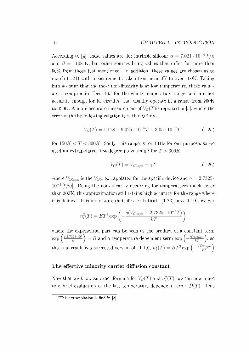
10 CHAPTER 1. INTRODUCTION
According to [4], these values are, for intrinsic silicon: α = 7.021 · 10−4 V/K
and β = 1108 K, but other sources bring values that dier for more than
50% from those just mentioned. In addition, these values are chosen as to
match (1.24) with measurements taken from near 0K to over 400K. Taking
into account that the most non-linearity is at low temperature, these values
are a compromise best t for the whole temperature range, and are not
accurate enough for IC circuits, that usually operate in a range from 200K
to 450K. A more accurate measurement of VG(T )is reported in [5], where the
error with the following relation is within 0.2mV.
VG(T ) = 1.178− 9.025 · 10−5T − 3.05 · 10−7T 2 (1.25)
for 150K < T < 300K. Sadly, this range is too little for our purpose, so we
used an extrapolated rst degree polynomial2 for T > 300K:
VG(T ) = VG0npn − γT (1.26)
where VG0npn is the VG0r extrapolated for the specic device and γ = 2.7325 ·10−4 [V/°C]. Being the non-linearity occurring for temperatures much lower
than 300K, this approximation still retains high accuracy for the range where
it is dened. It is interesting that, if we substitute (1.26) into (1.19), we get
n2i (T ) = ET 3 exp
(−q(VG0npn − 2.7325 · 10−4T )
kT
)where the exponential part can be seen as the product of a constant term
exp(
q·2.7325·104
k
)= B and a temperature dependent term exp
(− qVG0npn
kT
), so
the nal result is a corrected version of (1.19), n2i (T ) = BT 3 exp
(− qVG0npn
kT
)
The eective minority carrier diusion constant
Now that we know an exact formula for VG(T ) and n2i (T ), we can now move
to a brief evaluation of the last temperature dependent term: D(T ). This
2This extrapolation is nd in [3].

1.3. TEMPERATURE DEPENDENCE 11
term is given by
D(T ) = VT µn(T ) (1.27)
where µn is the average mobility for minority carrier in the base
µn(T ) = CT−n (1.28)
Accurate evaluation of Base-Emitter voltage temperature depen-
dence
Now that all the temperature dependent parameters of our IS(T ) have been
explicitly related to temperature, we can express VBE(T ) in its most general
and accurate form. Let us consider two temperatures: an arbitrary tem-
perature T and a reference temperature TR. Applying (1.8) for these two
temperature, we get VBE(T ) = kTq
ln(
IC(T )IS(T )
)VBE(Tr) = kTr
qln(
IC(Tr)IS(rrr)
) (1.29)
multiplying the rst equation for Tr and the second one for T and subtracting
them, we derive the following expression:
VBE(T ) =
(T
Tr
)VBE(TR) +
(kTr
q
)ln
[IS(Tr)
IS(T )· IC(T )
IC(Tr)
](1.30)
Let us now use (1.9) in (1.30), with n2i (T ) given by (1.20) and D(T ) given
by (1.27). This brings to the following relation3:
VBE(T ) = VG(T )−(
T
Tr
)VG(Tr)+
(T
Tr
)VBE(Tr)+
kT
qln
[(T
Tr
)4µ(Tr)
µ(T )
IC(T )
IC(Tr)
](1.31)
3Calculation in appendix (A.1)

12 CHAPTER 1. INTRODUCTION
and using (1.28) in(1.31) we get:
VBE(T ) = VG(T )−(
T
Tr
)[VG(Tr)− VBE(Tr)]− η
(kT
q
)ln
(T
Tr
)+
+
(kT
q
)ln
[IC(T )
IC(Tr)
](1.32)
where η ≡ 4 − n. A particular case for (1.32) happens when the collector
current is proportional to some power of T:
IC(T ) = FT x (1.33)
Using (1.33) in (1.32), we obtain a simplied expression for VBE(T ):
VBE(T ) = VG(T )−(
T
Tr
)[VG(Tr)− VBE(Tr)]− (η − x)
(kT
q
)ln
(T
Tr
)(1.34)
and using (1.26), our expression for VG(T ) related to our NPN transistor, we
get
VBE(T ) = VG0npn−(
T
Tr
)[VG0npn − VBE(Tr)− γTr]− (η−x)
(kT
q
)ln
(T
Tr
)(1.35)
1.3.2 Discussion on Approximations and Secondary Ef-
fects
The equations in subsec. 1.3.1 on page 6 have dierent degrees of precision,
from quasi-exact to high precision. One of the most widely used expression
for VBE(T ) is (1.34) (very often used with VG(T ) = ˆVG0). However, this case
does not occur so easily: temperature dependence of resistors used to set
IC(T ) can lead to a current that does not vary as described in(1.33). In this
case, (1.32) must be used and in order for this equation to be considered
valid, the following comments are needed:
1. µ is an eective mobility of the minority carrier in the base, but all
the existing data on mobility is for majority carrier instead. So we
1.3. TEMPERATURE DEPENDENCE 13
are assuming that the temperature dependence of the minority carrier
mobility is the same as the mobility of majority carriers in a material
of the opposite polarity and same doping concentration.
2. The constant in equation (1.28) depends on the impurity concentration.
For a standard PNP device it is reasonable to consider this constant
throughout the base. For a standard NPN device, the impurity con-
centration varies with depth, and therefore so do the constants in the
mobility expression. µ(T ) is a single eective mobility, so it takes into
account the global eect of all individual mobility. It follows, then,
that what is true for a specic impurity concentration is true for the
eective mobility.
3. Relation (1.28) is given at around room temperature and could not
be accurate in the whole temperature range of interest.
For these reasons, from case to case, we have to wisely consider which equa-
tion to use in relation to what kind of data and accuracy we want to obtain.
Let us now consider the intrinsic carrier concentration described in (1.20):
the quantity E is proportional to the average density-of-states eective mass
and this varies with temperature, but more complex expression for ni(T ) does
not lead to a signicant improvement[6]. Fabrication process must also be
considered, because they lead to a deviation of the parameter η in (1.35) and
from the basic relation described in (1.5). This relation become
IC(T ) = IS(T ) exp
(VBE(T )
αkT
)(1.36)
where α is slightly grater then 1, and is current and temperature dependent
and can change form device to device in the same wafer. Parasitic resistance
can also impact on the IC over VBE characteristic. Let us consider RC , a
collector series parasitic resistance. The intrinsic VCE will be
V′
CE = VCE −RCIC (1.37)

14 CHAPTER 1. INTRODUCTION
and this can become a problem, especially for low VCE, especially for a PTAT
IC where, for higher temperature, the VBE needed to support a given IC may
become higher than what would normally be required.
1.4 Compensation Orders
When designing a bandgap voltage reference, one of the main goals is to
achieve a temperature independent output voltage. To reach this purpose
in ICs domain, it is common to use devices or structures that have dierent
temperature dependence in order to sum their contribute, or even trying
to neglect every contribute exploiting some particular characteristic of the
device itself. Just as an example, refer to g.1.5 . This gure shows that if
Figure 1.5: N-channel MOSFET, Id over Vgs, temperature as parameter.
this n-channel MOSFET is biased with a precise current, its VGS shows very
little temperature dependence. If the source of this n-channel MOSFET is
grounded, its gate can be taken as a stable voltage reference. Needless to
say, we would need a current that should be constant over temperature, so the
problem just lays somewhere else. The bipolar transistor opens the possibility
of exploiting its VBE(T ) in order to get a temperature compensation with very
high precision. In sec. (1.3), we have derived dierent descriptions of the

1.4. COMPENSATION ORDERS 15
base-emitter voltage, from quasi-exact to very high precision approximation.
Let us recall (1.35)
VBE(T ) = VG0npn−(
T
Tr
)[VG0npn − VBE(Tr)− γTr]− (η−x)
(kT
q
)ln
(T
Tr
)(1.38)
and let us take a look at its temperature dependence: theVBE relationship
can be rewritten as
VBE(T ) = A + BT + Cf(T ) (1.39)
where f(T ) represents all terms whose order is greater than 1. Ok, so our
dream is to have Vref = A, or at least A + σ(T ) in the temperature range of
interest, but how can we get this result? One way is to use the Taylor series
expansion of VBE(T ) and try to compensate every order until the required
precision has been reached. Another way can be exploiting the (η−x) term,
forcing a collector current proportional to T η so that C=0 in (1.39) and easily
compensate the B term. It is also possible to try to compensate B and Cf(T )
directly. All these solutions need to be implemented with a circuital topology
that must also fulll many other specications other than extremely low
temperature sensitivity and not all the parameters that are visible on the
equation can be easily manipulated. The rst and second order compensation
of the Taylor series expansion of VBE(T ) is a very eective technique and
widely used for bandgap compensation, so it will be evaluated. The only
term to expand in (1.35) is (η − x)(
kTq
)ln(
TTr
), being the other terms of
zero or rst degree.
(η − x)
(kT
q
)ln
(T
Tr
)= (η − x)
VTr
Tr
[T ln
(T
Tr
)](1.40)
= K
[T ln
(T
Tr
)]= K
∞∑n=0
[an(T − Tr)
n
n!
](1.41)

16 CHAPTER 1. INTRODUCTION
with
ak =∂k[T ln
(TTr
)]∂kT
∣∣∣∣∣∣T=Tr
(1.42)
With calculation, we get
VBE(T ) = [VG0npn + (η − x)VTr ]
−(
T
Tr
)[VG0npn − VBE(Tr) + γTr + (η − x)VTr ]
+σ(T ) (1.43)
for the rst order expansion, and
VBE(T ) =
[VG0npn +
(η − x)VTr
2
]−(
T
Tr
)[VG0npn − VBE(Tr) + γTr]
−T 2
T 2r
VTr
[(η − x)
2
]+ σ(T 2) (1.44)
for the second order.We need to implement some circuits that can generate a
PTAT and a PTAT 2 signal. This blocks are essential not only for the straight
order to order compensation, but also for most complex bandgap structures
and pseudo-supply structures.
1.5 Functional Blocks: Current References
1.5.1 PTAT Current Generator
PTAT current reference can be implemented both with CMOS and bipolar
transistors. For our purpose, we will exploit the NPN bipolar properties.
Fig. 1.6 shows one possible implementation4.
4For more BJT and CMOS implementations, see [7].

1.5. FUNCTIONAL BLOCKS: CURRENT REFERENCES 17
Figure 1.6: PTAT current generator.
This circuit exploit the VBE(T ) logarithmic relation of eq. (1.8). Applying
KVL to the loop with Q1, Q2 and RPTAT , we get:
VBE1 − VBE2 −RPTAT IR = 0 (1.45)
Solving (1.45) for IR we get
IR(T ) =VT ln
(IC1(T )
Ae1JS(T )
)− VT ln
(IC2(T )
Ae2JS(T )
)RPTAT
(1.46)
=VT ln
(IC1(T )
Ae1JS(T )· Ae2JS(T )
IC2(T )
)RPTAT
(1.47)
Because of the current mirror and neglecting the base-currents5, we can write,
for (1.47):
IR(T ) =VT ln (K)
RPTAT
= T · k ln(K)
q(1.48)
where K = IC1
IC2. If RPTAT had zero order temperature dependence, this
current would be PTAT. We will see later in chapter 2 how this non-ideality
will impact on the overall errors and performances. The drawback of this
implementation is that it has a zero-current state, so it needs a start-up
5Errors will be discussed in subsec. 2.4.

18 CHAPTER 1. INTRODUCTION
in order to prevent the circuit from approaching this state. These PTAT
generators can be implemented also with lateral PNP structure, but these
topologies are less robust than the NPN counterpart because of two factors:
a low collector-current eciency (especially if a highly doped buried layer is
not available) and a lightly doped base region. The rst factor is due to the
existence of a parasitic vertical PNP transistor whose collector is connected
to substrate. As a result, some of the emitter current ows to substrate,
thereby reducing the collector-current eciency of lateral PNP device. The
second drawback is due to the decrease of the current gain (forward-β) with
increasing the collector-current because of high-level injection. This phe-
nomenon occurs when minority carrier density in the base region becomes
comparable with the majority carrier density. This happens because neutral-
ity must be maintained. Higher majority carrier density shorten the minority
carrier life (there are more majority carriers to recombine with) and increases
the eective doping density of the base. For proper operation, the minority
carriers should be well below the majority carrier level. This eect is still
present but less eective on NPN because of the highly doping density of the
base.
1.5.2 PTAT 2 Current Reference, Bipolar Implementa-
tion
A PTAT 2 current generator is also necessary in order to implement a precise,
second order compensated, voltage reference. The common circuital imple-
mentation is shown in Fig. 1.7. Considering KVL composed by transistor
Q1, Q2, Q3 and Q4 and using for each base-emitter voltage eq. (1.8), it yields
VT ln
[IPTAT 2
(IPTAT
A+ ICTAT
)IPTAT · IPTAT
]= 0 (1.49)
so
IPTAT 2 =I2PTAT(
IPTAT
A+ ICTAT
) ≈I2PTAT
K(1.50)

1.5. FUNCTIONAL BLOCKS: CURRENT REFERENCES 19
where
Figure 1.7: Bipolar PTAT 2 current generator.
IPTAT
A+ ICTAT ≈ constant (1.51)
This circuit however stacks two NPN transistor and so it is not suitable
for very-low voltage environment. Another way to get a PTAT 2 current
generator without vertical NPN stacking is shown in Fig. 1.8.
Figure 1.8: PTAT 2 current generator with horizontal NPN placement.

20 CHAPTER 1. INTRODUCTION
KVL for this circuit yields
VT ln
[Iout
(IPTAT +ICTAT
2
)IPTAT · IPTAT
]= 0 (1.52)
so again
Iout = IPTAT 2 =I2PTAT(
IPTAT +ICTAT
2
) ≈I2PTAT
K(1.53)
but this circuit needs less headroom then the one shown in Fig. 1.7. Both
the circuits suer of inherent errors and approximations that can invalidate
their precision. The most remarkable is due to the temperature coecient
of resistors used for generating the PTAT current that are CTAT in nature.
Their behavior is not linear with temperature but with quadratic law so its
eect will happen for high temperature, just where the second order compen-
sation should kick in. When this eect begins, the PTAT 2 current begins
to get linear, and the precision decreases. This interferes with (1.51) too
because, the higher the temperature, the more the ICTAT gets parabolic and
the more IPTAT gets at, thereby leading to a CTAT current.
1.5.3 The Output Stage
The output stage of the voltage reference must be designed according to the
load and the headroom limits for the given application. The main forms
for an output stage are three: voltage-mode, current-mode and mixed-mode.
Mixed-mode refers to circuits employing both voltage-mode and current-
mode techniques. Voltage-mode easily implements low-impedance output
stage but lacks the ability to choose the output level. On the other hand,
current-mode is not suitable for implementing low-impedance output, but
the output level can be easily regulated. If, for instance, the load is a large
capacitor, there may not be the need for a low-impedance output.
Voltage-Mode
The voltage-mode output is the most common technique and has been used
for long time because of its simplicity: in case of bandgap references, the
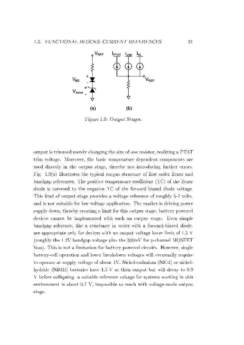
1.5. FUNCTIONAL BLOCKS: CURRENT REFERENCES 21
Figure 1.9: Output Stages.
output is trimmed merely changing the size of one resistor, realizing a PTAT
trim voltage. Moreover, the basic temperature dependent components are
used directly in the output stage, thereby not introducing further errors.
Fig. 1.9(a) illustrates the typical output structure of rst order Zener and
bandgap references. The positive temperature coecient (TC) of the Zener
diode is summed to the negative TC of the forward-biased diode voltage.
This kind of output stage provides a voltage reference of roughly 5-7 volts,
and is not suitable for low voltage application. The market is driving power
supply down, thereby creating a limit for this output stage: battery powered
devices cannot be implemented with such an output stage. Even simple
bandgap reference, like a resistance in series with a forward-biased diode,
are appropriate only for devices with an output voltage lower limit of 1.5 V
(roughly the 1.2V bandgap voltage plus the 300mV for p-channel MOSFET
bias). This is not a limitation for battery powered circuits. However, single
battery-cell operation and lower breakdown voltages will eventually require
to operate at supply voltage of about 1V. Nickel-cadmium (NiCd) or nickel-
hydride (NiMH) batteries have 1.5 V at their output but will decay to 0.9
V before collapsing: a suitable reference voltage for systems working in this
environment is about 0.7 V, impossible to reach with voltage-mode output
stage.
22 CHAPTER 1. INTRODUCTION
Current-Mode
A current-mode output stage is obtained summing temperature-dependent
currents into a resistor, as show in Fig. 1.9(b). This way, only the value of
the currents and of the resistor determine the value of the output voltage.
This conguration oers a wide spectrum of choices for the output voltage,
accommodating a range from millivolts to several volts. For most curvature-
corrected bandgap references, the currents involved are PTAT, CTAT and
non-linear. This makes possible to trim the output voltage simply by trim-
ming one of the components, usually the PTAT current. Moreover, even
though current-mode outputs suer the fact that, in most cases, PTAT and
CTAT current must be generated from a certain voltage over a resistance,
then mirrored, and then summed into a load, they still retain a low sensitiv-
ity to resistors TC. This happens because the transfer function between the
voltage that generates that current and its eect on the output voltage is a
resistor ratio, like:
Vout = VinRload
Rin
(1.54)
so the TCs of the resistors are deleted. However, the eectiveness and sim-
plicity of the voltage-mode is almost lost in the many errors occurring in
transferring the voltage input reference (PTAT, CTAT, etc..) to the output
load. This aspects will be further discussed in subsec. 2.4 of chapter 2.
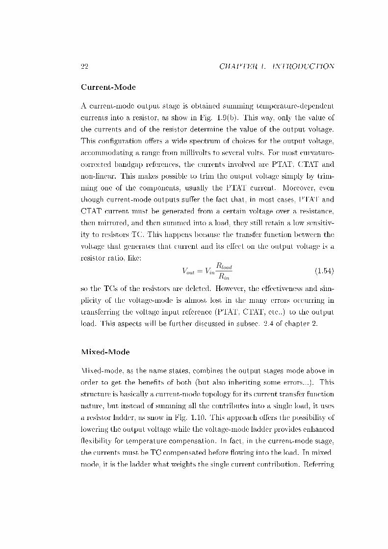
Mixed-Mode
Mixed-mode, as the name states, combines the output stages mode above in
order to get the benets of both (but also inheriting some errors...). This
structure is basically a current-mode topology for its current transfer function
nature, but instead of summing all the contributes into a single load, it uses
a resistor ladder, as snow in Fig. 1.10. This approach oers the possibility of
lowering the output voltage while the voltage-mode ladder provides enhanced
exibility for temperature compensation. In fact, in the current-mode stage,
the currents must be TC compensated before owing into the load. In mixed-
mode, it is the ladder what weights the single current contribution. Referring
1.6. IMPACT ON A VOLTAGE REGULATOR PERFORMANCE 23
Figure 1.10: Mixed-mode output topology.
to Fig. 1.10:
Vref = IVBE(R1 + R2 + R3) + IPTAT (R2 + R3) + INLR3 (1.55)
where IVBE, IPTAT and INL correspond to the base-emitter, the PTAT and
the nonlinear temperature-dependent currents respectively.
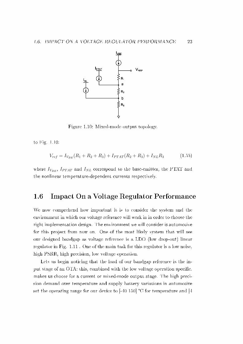
1.6 Impact On a Voltage Regulator Performance
We now comprehend how important it is to consider the system and the
environment in which our voltage reference will work in in order to choose the
right implementation design. The environment we will consider is automotive
for this project from now on. One of the most likely system that will see
our designed bandgap as voltage reference is a LDO (low drop-out) linear
regulator in Fig. 1.11 . One of the main task for this regulator is a low noise,
high PSRR, high precision, low voltage operation.
Lets us begin noticing that the load of our bandgap reference is the in-
put stage of an OTA: this, combined with the low voltage operation specic,
makes us choose for a current or mixed-mode output stage. The high preci-
sion demand over temperature and supply battery variations in automotive
set the operating range for our device to [-40 150] °C for temperature and [4

24 CHAPTER 1. INTRODUCTION
Figure 1.11: LDO linear regulator.
45] V for battery supply. Moreover, we want to guarantee a stable behavior
also in the [150 180] °C range, where leakage eects dominate and can make
over-temperature safe circuitry fail. The frequency range is set to be 10MHz
so to cover also DC-DC converter environment.
PSRR
In order to study the PSRR impact over the linear regulator system, it is
useful to describe it as a block diagram and, for doing so, we must also
explicit all the transfer functions that are going to describe it. Let us start
identifying the blocks.
Block Name Block Function Block Description
A VOT A(V+−V−)
The open loop gain of the OTA
BV0OT AVBIAS
The open loop transfer function from VBIAS to V0OT A
CV0OT A
VCCThe open loop transfer function from VCC to V0OT A
H 1 The feedback gain
LVref
VCCThe bandgap PSRR to Vref with no feedback from VBIAS
M VBIASVCC
The bandgap PSRR to VBIAS with no feedback from Vref
P VREFVG
Common source gain of the power stage
Q VREFVS
Common gate gain of the power stage
Table 1.1: Blocks table.
Now, suppose we have our signal Vin = VCC and VO = VREF , then we can
write the block diagram of Fig. 1.12. We can now write the equation that

1.6. IMPACT ON A VOLTAGE REGULATOR PERFORMANCE 25
Figure 1.12: Linear voltage regulator block diagram.
describe this system6:
[(VOH − LVin) A + VinMB + VinC] (−P ) + VinQ = VO (1.56)
VO
Vin
=P (LA−MB − C) + Q
1 + HPA(1.57)
We can write this equation in a more intuitive way: doing so and substituting
the diagram block letters with their meaning, we get
VO
Vin
=AOTAL−MB − C + ACG
ACS
1ACS
+ AOTA
(1.58)
Being 1ACS
AOTA, with AOTA ≈ 370 and 1ACS
≈ 0.2, we can write
VO
Vin
≈AOTAL−MB − C + ACG
ACS
AOTA
= L +
ACG
ACS− C −MB
AOTA
(1.59)
so we can write
PSRR = 20 log
(L +
ACG
ACS− C −MB
AOTA
)(1.60)
The OTA have C ≈ 1, value that is conrmed by the simulator in the whole
bandwidth of interest. The common-gate common-source ratio can be easily
6For full calculations see appendix A.2.1

26 CHAPTER 1. INTRODUCTION
calculated7 and it follows that
ACG
ACS
≈ 1 (1.61)
and, like for the C term, this can considered a constant for the frequency
range we are considering. A qualitative overview of eq. (1.60) tell us that the
PSRR is dominated by the worst (higher) term between L andACGACS
−C−MB
AOTA=
PSRRideal8. Practically, we can consider dominant the term that is about 5
times greater than the other term. This way, we get a shift of
20 · [log(5x)− log(5x + x)] = 20 · log(
5
6
)= 1.58dB (1.62)
It can come in handy to express the error shift in function of L and
ACG
ACS− C −MB
AOTA
= Γ
writing
εshift = −20 · log
(1 +
L
Γ
)(1.63)
From simulations of this LDO regulator, we get that the PSRRideal =
−103dB so our target will be to design a bandgap reference with about
a 15factor from linear PSRRideal, that in dB is 20log
(15
)= −14dB, and
what we expect is too get a PSRRsystem ≈ −100dB. All these calculations
are conrmed by simulation as it is shown in Fig. 1.13. Looking at Fig.
1.13 (a), there is a ∆PSRRsystem = 2.1dB for PSRRBG of -115dB (12dB
less than PSRRideal that is a x4 linear factor) where PSRRBG = 20 log(L).
Equation (1.63) gives εshift = −1.93dB, with good accuracy. Fig. 1.13 shows
that, if the bandgap reference has PSRR PSRRideal, then PSRRsystem =
PSRRBG. We now have a target for our PSRR, that, in order not to impact
on the performance of the regulator, must achieve a PSRRBG . −110dB.
Although all this dissertation regarded the DC part of the PSRR, AC speci-
7See [8], sec. 3.3.8Note that the MB term depends on how we choose to bias the OTA and must be
handled accordingly to the whole system.

1.6. IMPACT ON A VOLTAGE REGULATOR PERFORMANCE 27
cation will be treated in chapter 2.
Precision
Precision is one of the main matter with a voltage reference. Both design,
layout and production (components tolerance, packaging stress, etc..) are
involved. What we can do in order to achieve a good precision is to take into
account all the errors, random and systematic, that may (and will) occur,
both in the design and layout stage. Our goal for this voltage reference is to
reach high precision, ±1.5% for 3(
ση
), being σ the standard deviation and
η the average of the process.

28 CHAPTER 1. INTRODUCTION
Figure 1.13: (a)PSRRsystem in function of PSRRBG. (b)PSRRBG.

Chapter 2
Design
In chapter 1 we saw which specication we have to fulll. Our starting point
in this thesis was however the analysis of an already develop sub-Bandgap
structure. This analysis brought the main problems to light and showed
what are the structural and physical limits for a voltage reference. Trying to
overcome them will be our challenge.
2.1 The Second Order Curvature-Corrected
Sub-Bandgap
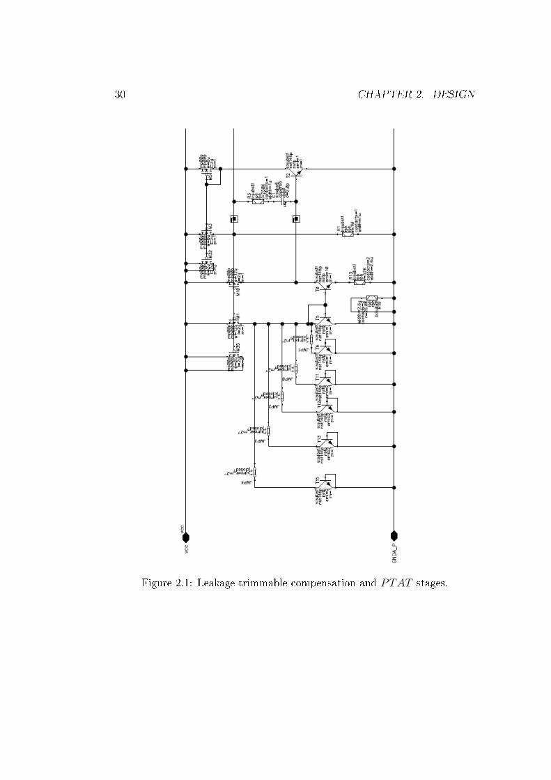
The proposed sub-bandgap voltage reference is a second order curvature cor-
rected, with mixed-mode output stage. Its schematic is in Fig. 2.1 and 2.2. It
presents the PTAT and low-voltage PTAT 2 stages seen in sec. 1.5 and uses
a NPN transistor with a constant IC(T ) to generate the VBE(T ) reference.
The mirrors are p-channel low-voltage MOSFETs mp00p with minimum
channel length and all the circuit but the PTAT 2 stage use nst146p NPN
standard transistor; PTAT 2 stage uses high-frequency oriented nhf112p. In
Fig. 2.1 we see also a leakage-compensation trimmable stage, whose imple-
mentation is done such to simplify a FIB (Focused Ion Beam) modication
to cut one the desired net that connects one ore more of the NPN transistors
connected to the drain of M1.
29
30 CHAPTER 2. DESIGN
Figure 2.1: Leakage trimmable compensation and PTAT stages.

2.1. THE SECONDORDER CURVATURE-CORRECTEDSUB-BANDGAP 31
Figure 2.2: Spt5 sub-Bandgap: CTAT , PTAT 2 and output stages.

32 CHAPTER 2. DESIGN
2.1.1 Design Overview
The mixed-mode resistor-ladder has been chosen as in Fig. 2.3, where IINDP
is the sum of a PTAT and CTAT current so that, once owing into a load,
the voltage they generate is constant in temperature. What really happens
is that IINDP = IPTAT + ICTAT so it gives a rst order compensated voltage
over the load. It is very important to take into account that, having all resis-
tors a certain TC (negative and quadratic for rph-poly resistors), a constant
current does not generate a constant voltage over the load. So IINDP will be
PTAT in nature, but with the TC that will compensate the resistors TC of
the load. This is why the resistors involved in translating a voltage signal
into current and those who will be the load for those currents must be of the
same type.
Figure 2.3: Output stage.
The output stage is congured in order to get the curvature compensation
in Fig. 2.4: the classic rst-order concave-down curvature is summed to a
concave-up curvature so to yield a at, second order compensated output.
As shown in Fig. 2.4(a), the concave-up curvature is obtained by the sum of
the PTAT 2 and the CTAT voltage.

2.1. THE SECONDORDER CURVATURE-CORRECTEDSUB-BANDGAP 33
Figure 2.4: Curvature correction scheme.
The equation used for VBE(T ) for this circuit is the Taylor series expansion
stopped at rst order of eq. (1.34), where VG(T ) has been considered constant
and equals to 1.2V. The VBE(T ) formula used in this design is then
VBEfirst(T ) = [VG0 + (η − x)VTr ]−
(T
Tr
)[VG0 − VBE(Tr) + (η − x)VTr ]
(2.1)
The x term has been considered 0 since ICT1≈ constant. Recalling eq.
(1.48), we have
IPTAT (T ) =Vt ln(10)
RPTAT
(2.2)
RPTAT is dimensioned to set the magnitude of the IPTAT (T ); this will set the
whole circuit current consumption because all the other stage will be supplied
by this current or have to compensate it, so they are strictly related to it.
Being VTr ln(10) ≈ 58mV , choosing RPTAT = 52kΩ sets the current to 1.1µA
at ambient temperature and the span will be [890nA− 1.73µA] considering
a [-40°C +180°C] temperature range. The rst order compensation will give
∂ICTATfirst(T ) + IPTAT (T )
∂T
∣∣∣∣T=Tr
= 0 (2.3)

34 CHAPTER 2. DESIGN
so it follows that
VTr ln(10)
TrRPTAT
=VG0 − VBE(Tr) + ηVTr
TrRCTAT
(2.4)
This gives straight forward a value for RCTAT
RCTAT = RPTAT ·VG0 − VBE(Tr) + ηVTr
VTr ln(10)(2.5)
Using the simulated value for VBE(Tr) and η = 4, RCTAT = 598kΩ ≈ 600kΩ.
IINDP is also set and it becomes
IINDP (T ) =A1T
RPTAT
+
[B1
RCTAT
− C1T
RCTAT
]
with A1 =VTr ln(10)
Tr, B1 = VG0 + ηVTr and C1 =
VG0−VBE(Tr)+ηVTr
Tr. Writing
the total output voltage, we can determine how to set load resistors seen in
Fig. 2.2 on page 31
Vref = ICONST ·(R15+R16+R17)+ICTAT ·(R16+R17)+IPTAT 2 ·R16 (2.6)
VBE(T ) must be written with its Taylor series expansion for the second order
so to calculate its second order coecient, the PTAT 2 compensation and
sizing R16 and R17. Doing so for eq. (1.34), again with the same approxi-
mations of eq. (2.1), we get
VBE(T ) =
[VG0 +
(η − x)VTr
2
]−(
T
Tr
)[VG(Tr)− VBE(Tr)]−
T 2
T 2r
[VTr
(η − x)
2
](2.7)
The PTAT 2 current has a not known coecient due to the its nature: it
is not the transduction of a voltage through a resistor, but the function
of another current, so the TC of the resistor generating the source current
(IPTAT in this case) does not cancel itself. What is possible to do, is to
estimate via simulation the law for R16 · IPTAT 2 and design R17 accordingly.
R16 is so chosen just as to maintain the eect of R16 · IPTAT 2 in the right
scale. Altering the circuit in order to evaluate VPTAT 2 = IPTAT 2 · (R16), we

2.1. THE SECONDORDER CURVATURE-CORRECTEDSUB-BANDGAP 35
are able to t its curvature with
VPTAT 2 = 0.3µT 2 − 75µT + 10.7m (2.8)
where the known term is just for tting purpose, giving precision to the high
range of temperature. Now we need that[∂VPTAT 2 + VBE
RCTAT(R16 + R17)
](T )
∂T
∣∣∣∣∣∣T=Tr
= 0 (2.9)
that yields
0.3µTr−75µ− VG(Tr)− VBE(Tr)
TrRCTAT
· (R16+R17)− VTrη
TrRCTAT
· (R16+R17) = 0
(2.10)
Easily inverting eq. (2.10), we get R16 + R17 ≈ 30kΩ, so R16 = 24kΩ.
2.1.2 Performance Overview
A second order curvature-compensated bandgap reference should achieve a
temperature drift performance from 1 to 20 ppm/°C [7], and we saw from
sec. 1.6 that we need a PSRRDC < −100dB in order not to invalidate
an hypothetical use in a voltage regulator. Another specication for more
demanding voltage regulators is a PSRR|f=10kHz < −70dB. We will however
evaluate the PSRR as function of VCC . Moreover, we are going to evaluate
the current consumption at nominal VCC = 3V in the temperature range of
interest and the minimum supply to turn on the bandgap reference and the
transient response to a10µs start-up with all node discharged and 10µs shut
down. Finally we will do a Monte Carlo analysis in order to see how process
and mismatch will aect the precision of the bandgap reference output. In
table 2.1, a quick view for this specications.

36 CHAPTER 2. DESIGN
Specication Value Passed
Precision 1 to 20 ppm/°C 17ppm/°C V
PSRRDC -100dB -45.7dB X
PSRR10kHz -70dB -23.62dB X
Low V oltage (≤ 1.4V ) Von < 1.4V 1.05V V
Monte Carlo ±1.5% for (3σ/media) ±13.1% for (3σ/media) X
Current Consumption @VCC = 3V lowest [16, 25, 40]µA for T [-40, 50, 180]°C ≈
Table 2.1: Specications table.
Fig. 2.5 shows the simulation results for this schematic. Using eq. 1.1,
we get
TCref =3m
795m/220°C= 17ppm/°C (2.11)
so the TC performance are in specication.
Figure 2.5: Sub-bandgap reference performance.

2.1. THE SECONDORDER CURVATURE-CORRECTEDSUB-BANDGAP 37
A statistical analysis has also been done for this bandgap. Even if the
accuracy required sets a range of values the reference must respect in order
to satisfy the specication (a normalized 3σ percentage for three dierent
temperatures is considered), we nd also important to keep track of the
bandgap TC. A bandgap reference that statistically suers of some oset
but has stable temperature behavior is dierent from a bandgap reference
with good bias at some reference temperature but with high TC. This way
we can evaluate how much imprecision is due to an oset eect and how much
to an error in TC. For this bandgap, we can see its process plus mismatch
statistical analysis in Fig. 2.6.
Figure 2.6: Monte Carlo Vref (T ) spread for three typical temperatures.

38 CHAPTER 2. DESIGN
Figure 2.7: TC 100% yield for V ref .
We can see in Fig. 2.6, we can see we have a 3σ spread , normalized over
the average, of
ε% = ±3 · 33.4m
763m· 100 = ±13.1%
These values have to be combined with those of Fig. 2.7: this gure shows
the percentage of samples that reaches a certain∆Vref
Vrefcalculated in the whole
220°C of temperature range. As stated in [7], a second-order compensated
circuit should have less than 50ppm/°C when realized. This means that we
should have a 100% yield for a value, in the x-axis graph of Fig. 2.7, of
xref = 50ppm/°C · T = 0.011
For that value, only the 22.3% of our samples are compliant.
2.1.3 Performance Evaluation
As we see from the previous subsec., nominal values for Vref and current con-
sumption are in specication, but Monte Carlo analysis reveals a weakness
to process and mismatch (most is due to mismatch, see subsec. 2.5.8). More-
over, the second-order compensation requires a lot of current to be drained

2.2. CHOOSING THE TOPOLOGY 39
from supply compared to the PTAT and CTAT stages because of the many
branches involved in the PTAT 2 current generation. The PSRR specica-
tion is just too high for a simple voltage reference1. We will have to nd
another solution for accomplish this task. We than see a strange behavior of
Vref for temperatures above 150°C. This is due to pn junction leakage cur-
rents. This phenomenon is very hard to compensate because it involves all the
transistors in the circuit and all contributions have dierent weights depend-
ing on each transistor area and bias. This circuit has a leakage-compensation
trimmable stage that tries to compensate this eect, but measurements will
show that this strategy is eective only for a precise supply voltage. Leakage
is also not precisely modeled in the simulator, so its compensation will require
careful evaluations. Last but not least at all, the transient response shows a
nervous behavior of the reference voltage when the supply is turned on and
o; this shows an overshoot tendency that may not be acceptable, and must
be taken into account while designing the loops frequency compensation.
Even though it is possible to redesign this circuit to better match all the
performance required (and this will be done in sec. 2.6), some stages and
design choices prevent further improvements. In order to create a state of
the art voltage reference, we will now start a new design, beginning from
the evaluation of the best-suited topology for our purpose and designing
every stage aiming to prevent or reduce the errors before they occur and
improving the synergy within the functional blocks of the circuit by avoiding
errors propagation.
2.2 Choosing the Topology
In [7] we can nd lots of ideas for voltage reference topology, but few envisage
doing low-voltage low-current high precision voltage reference. Among the
few, the one that best seems to suit our needs is the Diode Loop topology.
The circuit in Fig. 2.8 describes the idea over which this topology is based.
The trick consists in generating a non-linear voltage that tries to match ex-
1See subsec. 2.5.5
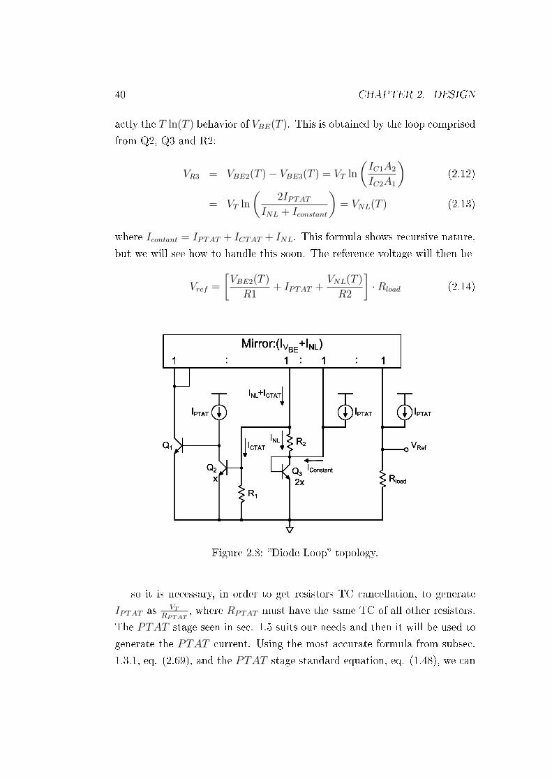
40 CHAPTER 2. DESIGN
actly the T ln(T ) behavior of VBE(T ). This is obtained by the loop comprised
from Q2, Q3 and R2:
VR3 = VBE2(T )− VBE3(T ) = VT ln
(IC1A2
IC2A1
)(2.12)
= VT ln
(2IPTAT
INL + Iconstant
)= VNL(T ) (2.13)
where Icontant = IPTAT + ICTAT + INL. This formula shows recursive nature,
but we will see how to handle this soon. The reference voltage will then be
Vref =
[VBE2(T )
R1+ IPTAT +
VNL(T )
R2
]·Rload (2.14)
Figure 2.8: Diode Loop topology.
so it is necessary, in order to get resistors TC cancellation, to generate
IPTAT as VT
RPTAT, where RPTAT must have the same TC of all other resistors.
The PTAT stage seen in sec. 1.5 suits our needs and then it will be used to
generate the PTAT current. Using the most accurate formula from subsec.
1.3.1, eq. (2.69), and the PTAT stage standard equation, eq. (1.48), we can

2.2. CHOOSING THE TOPOLOGY 41
write Vref as
Vref =
VG0npn −
(T
Tr
)ΘTr − (η − x)
(kT
q
)ln
(T
Tr
)· Rload
R1
+VT ln (K)
RPTAT
·Rload +VT
R2ln
(2IPTAT
INL + Iconstant
)·Rload (2.15)
with ΘTr = VG0npn − VBE(Tr) − γTr is constant. It is immediately visible
that we should be able to get a perfect cancellation of both the linear and
the T ln(
TTr
)to get Vref ≈ VG0npn. The headroom limitation is ultimately
dened by a diode-connected transistor, a drain-source voltage and a rela-
tively small resistive voltage drop, which results in a voltage headroom limit
of about 1V. We will now go through the implementation of this topology. In
Fig. 2.9 we can see the nal circuit in one of its three versions, divided into
functional blocks. The main block is for sure the PTAT stage, which sets
the main variables for the whole circuit, so it will be the start of the design
process. It is also the main source of errors. The CTAT and non-linear stage
will be sized after the PTAT stage. The output stage is fully current-mode
approach, to suite the low voltage requirement and because it is possible to
sum currents that do not need a resistor ladder. The chosen PTAT stage
has a zero-current steady state, so it needs a start-up circuitry in order to
work in the right state. This version includes a full leakage compensation
and many output pins for testing purpose.

42 CHAPTER 2. DESIGN
Figure 2.9: Diode Loop Bandgap Core V2 (full version).

2.3. PRELIMINARY PTAT STAGE ANALYSIS 43
2.3 Preliminary PTAT Stage Analysis
Tr is the reference temperature, and it is where the bandgap is more precisely
compensated. The more is the distance from Tr, the more the errors are
amplied. We decided to set Tr = 333K, so that Vref is compensated at its
mean value: setting Tr = 300K would have left a very larger temperature
range on the hotter side than it would on the colder side: this way, the error
is distributed equally over the temperature range.
Figure 2.10: The PTAT Stage.

44 CHAPTER 2. DESIGN
It will now be shown how the PTAT stage of Fig. 2.10 has been designed.
The rst component that we are going to determine is the area ratio between
T1 and T0. Area ratio for NPN device is well modeled and precise: using the
maximum ratio will grant higher accuracy over the generated current, much
higher than a resistor ratio. So the maximum value for Ae0 has been chosen:
Ae0
Ae1
= 10 (2.16)
We can now choose the value of R55. This is set so to have a quiescent
current of about 1µA at T = Tr. Using eq. (1.48)
VTr ln (K)
R55= 1µA (2.17)
R55 ≈ 60kΩ (2.18)
For values above 50kΩ, rph poly silicon resistors are used. These resistors
have a CTAT temperature coecient and this must be taken into account
when using them to transduce a voltage into a current. In order for eq. (1.48)
to be valid, let us write eq. (1.47) for this specic case:
IE0 =VT ln
(IC1(T )
Ae1· Ae0
IC0(T )
)RPTAT
(2.19)
Eq. (2.19) shows that IC1
IC0(T ) must be constant over temperature. This task
is performed by a loop that senses the dierence Iε(T ) = [IC0 − IC1] (T )
and regulates the mirror in order to minimize this error. This is necessary
because of the dierent VBE over IC characteristics of T0 and T1. T0 is of an
emitter-degenerated transistor while T1 is not, so they will behave as shown
in Fig. 2.11: T0 has a greater IC for low VBE because of the low IC itself that
cause little voltage drop on the degenerating resistor and it has bigger area,
but for higher VBE, the IC suer the degeneration due to R55, the PTAT
resistor; T1 has lower area, so for low VBE, the IC is smaller, but for higher
VBE and IC , it is free from degeneration, so the current can rise higher than
the collector-current of T0.

2.4. ERRORS COMPENSATION DETAILED ANALYSIS 45
Figure 2.11: IC over VBE characteristic.
In order to fully comprehend and successfully design the PTAT stage,
now that we placed all the components, it is necessary to study the many
errors aecting this stage before beginning the sizing of the components.
This is necessary because of the high precision required. In fact, if we want
to achieve a precision of few ppm over the [-40 150]°C range, we have to stay
under about 150µV of ∆Vref . We are biasing a load of about 400kΩ, so it
takes only 0.5nA on the output bias current to have a error of 200µV !
2.4 Errors Compensation Detailed Analysis
There are many sources of errors in thePTAT stage. We are now going to
evaluate them one by one in order to comprehend how they impact on the
output voltage, in relation to temperature.
2.4.1 Collector Current Mismatch
We can see in VPTAT (T ) = VT ln(
IC1(T )Ae1
· Ae0
IC0(T )
)that if IC1(T )
IC0(T )6= 1, VPTAT (T )
is not linear with temperature anymore but it will become function of the
collector-current ratio. There are two main sources of currents that can
impact on the collector-current ratio: the base currents and the leakage cur-
rents. Moreover, we must not forget that we are inside a loop, so not only
these currents will aect the VPTAT generation, but will also be mirrored on
the load and, beware, both these processes depend on the loop. This loop
consists of two nested loops and must be studied before more considerations
could be made.
46 CHAPTER 2. DESIGN
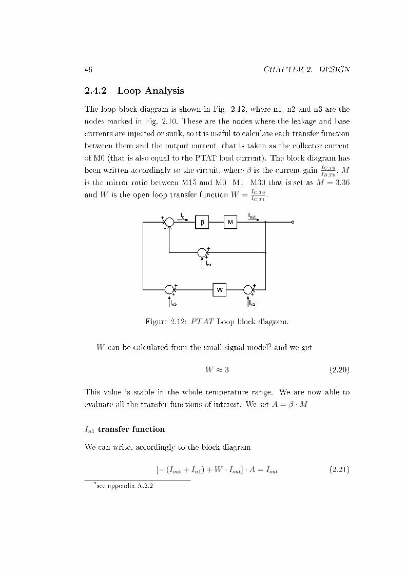
2.4.2 Loop Analysis
The loop block diagram is shown in Fig. 2.12, where n1, n2 and n3 are the
nodes marked in Fig. 2.10. These are the nodes where the leakage and base
currents are injected or sunk, so it is useful to calculate each transfer function
between them and the output current, that is taken as the collector current
of M0 (that is also equal to the PTAT load current). The block diagram has
been written accordingly to the circuit, where β is the current gainIC,T8
IB,T8, M
is the mirror ratio between M15 and M0=M1=M30 that is set as M = 3.36
and W is the open loop transfer function W =IC,T0
IC,T1.
Figure 2.12: PTAT Loop block diagram.
W can be calculated from the small signal model2 and we get
W ≈ 3 (2.20)
This value is stable in the whole temperature range. We are now able to
evaluate all the transfer functions of interest. We set A = β ·M
In1 transfer function
We can write, accordingly to the block diagram
[− (Iout + In1) + W · Iout] · A = Iout (2.21)
2see appendix A.2.2

2.4. ERRORS COMPENSATION DETAILED ANALYSIS 47
from which we getIout
In1
= 0.497 ≈ 0.5 (2.22)
In2 transfer function
For this current, we have that
[(Iout + In2) ·W − Iout] · A = Iout (2.23)
from which we getIout
In1
= 1.497 ≈ 1.5 (2.24)
In3 transfer function
For the conventions used for this loop analysis, the current In3 has the op-
posite sign of the verse indicated by the arrow in Fig. 2.12. So we get
[−Iout + In3 + W · Iout] · A = Iout (2.25)
Iout
In3
=1
1−W≈ −0.5 (2.26)
where K = AA−1
≈ 1. This result was predictable due to the fact that, in the
circuit, this current is the same as In1 even though in the block diagram it is
taken from another branch. This is due to the fact that in the circuit these
two currents are being taken from the same metal, so are practically the same,
while in the block diagram they are placed under or above the node where
the error current is generated, hence the dierent sign convention. Now that
we know how the loop reacts, we can go move further for more specic error
analysis.
2.4.3 Base Currents
We aimed to prevent the error due to the base-currents of T0, T1 and T52.
We choose an NPN transistor over a n-channel MOSFET so to sink a base-
current from the branch where it is connected. We dimensioned its area and

48 CHAPTER 2. DESIGN
collector-current so that it would sink the same current sunk from the bases
of T0, T1 and T52. This way, in rst approximation, being T0, T1 and T52
driving all the same IC and having very similar bias, they have the same
base-current, so we can writeIM0 = IC0 + 3IB (a)
IM1 = IC1 + 3IB (b)(2.27)
Subtracting (2.27)(b) to (2.27)(a) we get
IC0 − IC1 = Iε = IM0 − IM1 (2.28)
This way, we can reduce the error in the VPTAT generation that would be
caused by a dierence in the two collector currents IC0 and IC1. The draw-
back is that the output current carries also those 3IB to the output, requiring
an additional correction for their compensation
Vref (T ) = V′
ref + IB,tot(T )Rload(T ) (2.29)
where IB,tot is the total amount of current that the PTAT and NL stage cause
to ow on the output load. This compensation involves also the resistor TC
of the load, so we will model the
Vref,B = IB,tot(T )Rload(T ) (2.30)
term for a correct compensation. Exporting the data for (2.30), and tting
it with a rst and a second order polynomial, we get two expression
Vref,B(a) = −30µT + 0, 0318 (2.31)
Vref,B(b) = 80nT 2 − 800µT + 0, 0319 (2.32)
The rst order expansion has been calculated so to minimize the error on the
whole temperature range instead of having a precise tting for Tr and will
be our rst try into the compensation process.

2.4. ERRORS COMPENSATION DETAILED ANALYSIS 49
2.4.4 Mirror Channel Length Modulation and NPN Early
Voltage
The current mirrored from M0 and M1 can suer of a slight channel length
modulation. They share the same overdrive, but VDS,M1 = VCC − VCE,T1
while VDS,M0 = VCC−VBE,T0−VPTAT . This dierence is less than 6mV and,
for the transistor length chosen of 25µm and the bias, the error current is
negligible (magnitude of pico-ampere).
NPN Early voltage has more severe consequences on the PTAT stage.
The dierent VCE for T0 and T1 can cause an error on the PTAT voltage
over R55. We can write eq. (1.8) taking into account the Early voltage; we
get
VBE(T ) = VT ln
IC
AeJs
(1 + VCE
VA
) (2.33)
where VA is the Early voltage. We can now write the IPTAT relation using
(2.33) and it yields
IPTAT =VT
RPTAT
ln
K ·IC1
(1 + VCE0
VA
)IC0
(1 + VCE1
VA
) (2.34)
where K is the area ratio. It is easy to write IPTAT as a nominal current plus
an error current using the product property of logarithmic:
IPTAT =VT
RPTAT
ln
(K · IC1
IC0
)+
VT
RPTAT
ln
(1 + VCE0
VA
)(1 + VCE1
VA
) (2.35)
= I′
PTAT + IPTAT,error (2.36)
Using the Early voltage for our technology we get a total error on Vref
Vref−error = IPTAT,error ·Rload (2.37)
=Rload
RPTAT
· kT
q· ln(0.9998) (2.38)

50 CHAPTER 2. DESIGN
This error is about −140nV°C, so we would have a total error over the whole
temperature range of just −30µV and normally does not need any compensa-
tion. However, simulation results in Fig. 2.13 show an unexpected behavior
for VBG, the output voltage of our circuit, when hot temperatures, above
100°C, are reached. This gure shows also the error on the VPTAT voltage.
Fig. 2.14 shows the three topologies which realize the three simulation results
of Fig. 2.13.
Figure 2.13: Early voltage and saturation region approaching eects.
The ideal compensation consists in adding a VDC voltage generator which
supplies the dierence of the two collector-emitter voltages. The resistor
compensation consists in placing a resistor which causes a voltage drop to
reduce the collector-emitter voltage dierence. These, beyond the fact that
only one is physically feasible, dier because the rst one rises the voltage
collector of T0, the other one lowers the voltage collector of T1. We can
see that the error from a non-compensated situation, for temperature below
100°C, is negligible both with the resistor and ideal compensation. Above
100°C, we can see the eect shown in Fig. 2.13. In order to make proper
evaluations, we also keep track of the ratio IC1
IC0shown in Fig. 2.15, the
other source of error in the PTAT voltage generation. Let us examine the
case no compensation VS ideal compensation: we have a shift over all

2.4. ERRORS COMPENSATION DETAILED ANALYSIS 51
the temperature range, but we see no changing until 100°C. Moreover, with
the ideal compensation, IC0 becomes greater than IC1 for T ≈ 145°C and
should cause the error VPTAT,error to became negative; the non compensated
topology has a much more linear error behavior. However, the error on
VBG has the opposite behavior, but why? The resistor compensation case
shows more coherency between the VPTAT,error and VBG. The explanation
is that there is the superposition of two eects: the VPTAT,error and the
leakage-currents error. The operative point hypothesis does not give a full
Figure 2.14: Early voltage test topology.
Figure 2.15: Collector-currents ratio.

52 CHAPTER 2. DESIGN
explanation to these phenomena and it is not explainable through precise
formulas. We will see that the other source of error is the leakage current of
the parasitic PNP transistor and the parasitic diode. A deep insight in the
leakage current phenomenon is then required. Then, in Sec. 2.4.5, a solution
is formulated.
2.4.5 Leakage
With leakage current we mean the current in a reverse-biased pn junction.
This current is usually negligible for our bias range and for temperature under
100°C, but for T > 100°C, it increases exponentially from less than 1pA to
tens of nano-Ampere. This current is usually taken not as function of the
reverse bias, and even though it has little sensitivity to reverse bias changes,
measurements on the proposed sub-bandgap circuit showed that the leakage
compensation performed worked ne for just one precise voltage3. Fig. 2.16a
shows the main parasitic junction that cause current leakage. The D terminal
is connected to a substrate ring that is connected to ground.
(a) Parasitic PNP transistor and diode. (b) Leakage modelization.
Figure 2.16: Leakage parasitic devices and model.
Those junctions, once leaking, drain more current from the real collector
of the device, altering the total amount of current available for the main
3see chapter 3.

2.4. ERRORS COMPENSATION DETAILED ANALYSIS 53
device. In the PTAT stage, leakage currents not only cause an exponential
oset current (with temperature) that will be mirrored at the output load
with a transfer function determined by where they are injected in, but they
also cause an error in the IC − VBE characteristic, as can be seen in eq.
(2.35) when the IC ratio becomes temperature dependent. Let us examine
the physics behind this reverse current.
Leakage Physics4
In a pn junction, if a eld is present, we will have both diusion and drift
current. Electron current density will be
Jnx = qnµnEx + qDn∂n
∂x(2.39)
where Dn = kTq
µn (as in eq. (1.9), but here the electrons mobility µn has not
been taken as average) and n are the free carrier (electrons). These relation
is valid also for the hole diusion current
Jpx = qpµpEx − qDp∂p
∂x(2.40)
where the negative sign arises because of the positive charge of a hole. At
thermal equilibrium, the total current (so also the current density) for both
electrons and holes is zero, so we can write
qnµnEx + qDn∂n
∂x= 0 (2.41)
qpµpEx − qDp∂p
∂x= 0 (2.42)
from which we get (for the electrons)
n(x)∂V (x)
∂x=
Dn
µn
∂n(x)
∂x(2.43)
4For a complete physical analysis, please refer to [9]

54 CHAPTER 2. DESIGN
this equation yield to the integer relation∫ V 2
V 1
∂V (x) =
∫ n2
n1
1
n(x)∂n(x) (2.44)
so we can nally write that
V 2− V 1 = VT lnn2
n1
(2.45)
and, dually for holes
V 2− V 1 = VT lnp1
p2
(2.46)
These relation remain valid also for biased pn junction if the low-injection
hypothesis is respected. In this case, noticing that
holes concentration are equal to NA in the p-doped region and p2 =
pn (xn) in the n-doped region
electrons concentration are equal to ND in the n-doped region and
n1 = np (−xp) in the p-doped region
and supposing to have a reverse bias VA < 0 we can write (i.e for holes) that
V0 − VA = VT ln
(NA
p2
)(2.47)
from which we can nd the holes concentration as
p2 = pn (xn) = NAe
“VA−V0
VT
”= pn0e
“VAVT
”(2.48)
where pn0 = NAe−V0VT , that is when no bias is applied to the junction. For
electrons, we get
n1 = np (−xp) = NDe
“VA−V0
VT
”= np0e
“VAVT
”(2.49)
Dening
p′
n(x) = pn(x)− pn0 (2.50)

2.4. ERRORS COMPENSATION DETAILED ANALYSIS 55
For x > xn, p′n(x) can be obtained from continuity equation and we get
p′
n(x) = pn0
(e
VAVT − 1
)e−x−xn
LP (2.51)
where LP =√
DP τP is the diusion length and τp is the hole-lifetime. In our
case, our NPN transistor has a highly doped collector diusion, and can be
demonstrated that in a reverse bias situation, if ND NA, the drift current
is mainly given by electrons minority carriers, so we get that
Jr,drift = q
√Dn
τn
np0
(1− e
VAVT
)= q
√Dn
τn
n2i
NA
(1− e
VAVT
)(2.52)
This current density is given by the minority carriers who are injected from a
quasi-neutral region into the depletion region, but we must take into account
also the current due to electron-hole pair generation in the depletion region.
This current is given by
Jr,gen =qniW
τe
(2.53)
where τe is the eective life time of the carriers a W is the depletion-layer
width. τe varies slowly with temperature and will be considered constant in
the nal evaluation. W is function of the applied eld and it varies as
W (Va) = Wd0 ·√
1− VA
V0
(2.54)
where Wd0 is the depletion width when no eld is applied and V0 is the built-it
potential∣∣∣φi
q
∣∣∣. We can now write a proper formula for Jr:
Jr = q
√Dn
τn
n2i
NA
(1− e
VAVT
)+
qni
τe
Wd0 ·√
1− VA
V0
(2.55)
This formula shows that the reverse current
Ir = Aeff · Jr (2.56)

56 CHAPTER 2. DESIGN
is function both of the temperature and voltage. Despite it has not been
possible to evaluate Jr,drift and Jr,gen contribution for our technology, some
important observation can still be done. Supposing a typical value for V0 of
0.7V, if the drift and generation contribution are of the same magnitude we
can see that:
Dening VR = |VA|, if Vr > 3VT , Jr,drift does not change signicantly
with VA: in our case we have at least about 300mV at T=180°C for the
lower biased NPN transistor, so Vreverse ≈ 10VT . The change in this
bias range is about 50ppm from 150 to 180°C. This error is negligible.
Generation current shows that the reverse bias can aect the total
leakage current, especially if the applied voltage become severe. This
will explain also some behavior that will be shown and analyzed in
chapter 3. Considering qni
τeWd0 as not being function of the reverse
voltage applied, the term√
1− VA
V0shows great inuence by the applied
bias.
This last consideration impacts over two dierent situations:
On the NPN transistors: with the decreasing of collector voltage from
150 to 180°C from about 360mV to 300mV for all the NPN transistor
in the PTAT stage (neglecting the feedback transistor), Jr,gen decrease.
However, the changes can be easily calculated using eq. (2.54) and the
total change is about -4%. This error is negligible, and is also reduce by
the leakage compensation design. However, the leakage compensation
done at the output5 will suer this eects, because the output voltage
that is reverse-biasing the leakage compensation stage is xed at about
800mV while the leaking junctions are biased from 360mV to 300mV,
causing a Jr,gen overcompensation of about 15%.
On the p-channel MOSFETs: increasing the supply voltage in its range
of operation (i.e. 1.5V to 5V), using eq.(2.54) we get a Jr,gen leakage
increase of 70% for the p-channel MOSFETs in the PTAT stage and
5Explained in sec. 2.5

2.4. ERRORS COMPENSATION DETAILED ANALYSIS 57
90% increase for the p-channel MOSFETs in the output stage! This
error could be symmetrical in the PTAT stage and so arises negligible
errors, but it adds a voltage dependent current oset at the output. If
the bandgap reference is designed to work with dierent supply volt-
age, then a compensation must be designed. However, if the bandgap
reference is supplied by a pre-regulator or pseudo-supply, the need for a
leakage-mirror correction is not necessary: leakage currents injected by
p-channel MOSFETs to the load can be taken into account when choos-
ing what counter-measures to take for the whole leakage phenomenon.
In Sec. 2.5 we will analyze some techniques in order to compensate these
eects. Anyway, it is now possible to give an exhaustive explanation to the
nal issue nd in Sub-sec. 2.4.4 on page 49. Using the loop transfer functions
and applying them to the leakage currents, we get (for T=180°C)
Compensation In1 = |−In3| In2 Iout = 1.5In2 − 0.5In1
None 23nA 22.5nA 22.25nAIdeal (-60mV) 23nA 23.3nA 23.45nA
Resistor 21.5nA 22.5nA 23nA
Table 2.2: Leakage explanation to Vref variation discussed in 2.4.4.
Table 2.2 shows that we have a variation on the leakage that is transferred
to the output load. This eect must be added to the VPTAT,error of each
single case, shown in Fig. 2.13 on page 50. For 180°C, the error VPTAT,error,
calculated as dierential from the non compensation version, is:kTq
Rload
RPTAT·∆VPTAT,res
∣∣∣T=(273+180)K
≈ 600µV for res. compensation
kTq
Rload
RPTAT·∆VPTAT,ideal
∣∣∣T=(273+180)K
≈ −180µV for ideal compensation
(2.57)

58 CHAPTER 2. DESIGN
So the total error on the output stage, calculated as dierential from the non
compensated case, is600µV + (23− 22.25)n · Rload|T=180°C = 850µV for res. compensation
−180µV + (23.45− 22.25)n · Rload|T=180°C = 400µV for ideal compensation
(2.58)
These values does still not match with those reported in Fig. 2.13 on page 50.
This is because the other stages of the circuit depend on the PTAT reference
generated in this early stage, and they generate other errors correlated to the
errors of PTAT stage. However, it is already intuitive that if VPTAT
RPTATwill be
used for biasing other components (like the NPN who generates the CTAT
voltage reference), the error on the total output current of the PTAT stage
will cause an error of the same sign on the VBE(T ) generated and this will add
its contribute to the total error seen on VBG, hence supplying the dierence
between what we calculated and the simulation.
2.5 Diode Loop Topology Design
Now that we are aware of all the snares hidden in this topology, we can begin
sizing the components and implementing solutions for the main problems seen
in Sec. 2.4. Three version of this topology have been developed. Version 1 is
the default version, version 2 has a more accurate leakage compensation and
dierent test structures and version 3 is leaned towards area optimization.
2.5.1 The PTAT Stage
In Sec. 2.3 we began to build our PTAT stage. We sized the PTAT resistor,
R55 = 60kΩ and the area ration between T0 and T1 so to be Ae0
Ae1= 10. We
recopy again the PTAT stage for convenience in Fig. 2.17 on the next page.
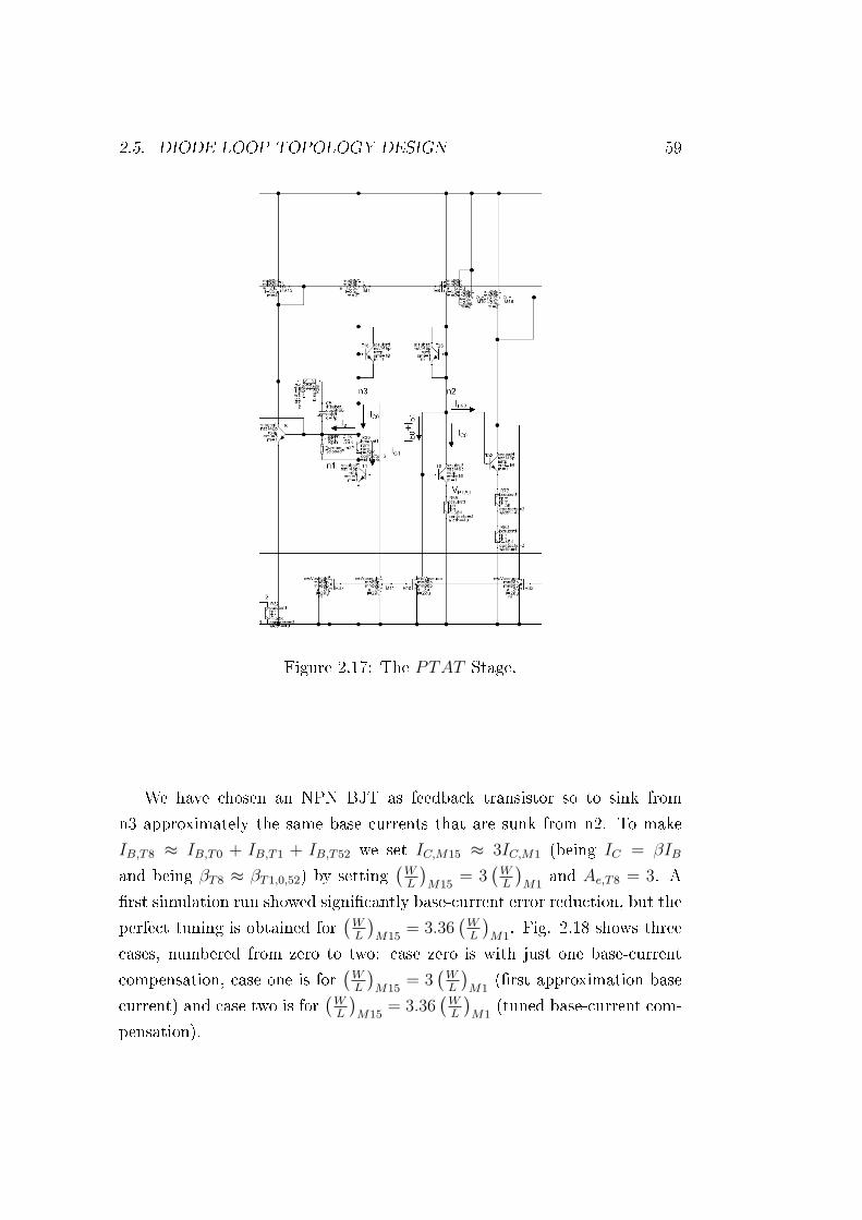
2.5. DIODE LOOP TOPOLOGY DESIGN 59
Figure 2.17: The PTAT Stage.
We have chosen an NPN BJT as feedback transistor so to sink from
n3 approximately the same base currents that are sunk from n2. To make
IB,T8 ≈ IB,T0 + IB,T1 + IB,T52 we set IC,M15 ≈ 3IC,M1 (being IC = βIB
and being βT8 ≈ βT1,0,52) by setting(
WL
)M15
= 3(
WL
)M1
and Ae,T8 = 3. A
rst simulation run showed signicantly base-current error reduction, but the
perfect tuning is obtained for(
WL
)M15
= 3.36(
WL
)M1
. Fig. 2.18 shows three
cases, numbered from zero to two: case zero is with just one base-current
compensation, case one is for(
WL
)M15
= 3(
WL
)M1
(rst approximation base
current) and case two is for(
WL
)M15
= 3.36(
WL
)M1
(tuned base-current com-
pensation).

60 CHAPTER 2. DESIGN
Figure 2.18: IB compensation results.
For each case, we can see how the error propagates on the VPTAT genera-
tion, changing the collector-current ratio of eq. (2.35), and nally aicts the

2.5. DIODE LOOP TOPOLOGY DESIGN 61
output voltage. As we see from Fig. 2.18, this error would aict the output
voltage very hard if not compensated.
The collector current ratio is sensitive also to the leakage current mis-
match of T0 and T1. As we have seen in eq. (2.56), leakage current is
proportional to the eective area where Jr ows. T0 and T1 have very dif-
ferent area ratio so their leakage currents are dierent. This causes an error
on the collector-current ratio in eq. (2.35). As we saw in subsec. 2.4.5, Fig.
2.16b, the eective collector current available for the transistor is reduced
by the leakage current, so the bigger the transistor is, the more its collector
current will drop. If we look at eq. (2.35), IC0 is at denominator, so, suer-
ing more leaking, it will cause a positive VPTAT error. This error will sum to
the error due to leakage currents being mirrored to the output so it will not
compensate itself, having both eects leaning towards the same direction.
This error can be compensated in many ways, more or less accurate, but all
of them will take advantages of the structure shown in Fig. 2.19
Figure 2.19: Leakage compensation NPN.
We will refer to this structure as anti-leakage conguration. Short-
circuiting all three terminals as shown in Fig. 2.19(a), we get a turned
o transistor which has only the parasitic diode and the pn junction of the
parasitic PNP enabled as can be seen in Fig. 2.19(b). We have got a structure
that only produce leakage current and is turned-o for T<120°C. We can use
this structure to sink leakage current from the net of interest. It is necessary
to make an important observations before proceeding: the eective area for
(2.56) is not strictly proportional to the emitter area used for the transistor:

62 CHAPTER 2. DESIGN
table 2.3 will summarize the value obtained from the simulator for a reverse
voltage VA = −800mV normalized for the leakage of an NPN with Ae = 1,
which value is about 8.5µA. This is due to the fact that the eective leaking
Ae 1 2 3 4 5 6 7 8 9 10
Ileak(1)Ileak(Ae)
1 1.088 1.177 1.266 1.354 1.443 1.429 1.5 1.572 1.644
Table 2.3: Leakage values for VA = −800m.
area depends also on the side area of the NPN. Multiplying the area does
not increase the perimeter area as placing two space transistor having the
same amount of area because, if these two transistor are put into contact,
the leakage from the touching sides is deleted. We have developed three
solutions.
1. The rst and more precise solution is the one used in this version of the
Diode Loop Sub-Bandgap6. It consists in adding two short-circuited
NPN (T16 and T25 of Fig. 2.17) for each branch of the PTAT circuits
that has the area of the transistor in the other branch. This way,
each collector current sees the same leakage and the error is precisely
compensated, as it come thatIC0 = IM0 − Ileak,1 − Ileak,10
IC1 = IM1 − Ileak,1 − Ileak,10
(2.59)
where Ileak,x is the leakage area for a single NPN transistor with Ae = x
and IM0 = IM1. The downturn is that we add more leakage current
that must then be sunk by the same structure at the output. The
amount of leakage current can be calculated by exploiting the block
diagram used for the loop study in Sub-sec. 2.4.2. We have that the
total leakage current mirrored to the output from the PTAT stage is
Ileak,OUT = (IL,T0 + IL,T25) 1.5− (IL,T1 + IL,T16) 0.5 (2.60)
= Ileak10 + Ileak1 (2.61)
6Version #2

2.5. DIODE LOOP TOPOLOGY DESIGN 63
Again, notice that Ileak10 + Ileak1 6= Ileak11. This leakage current will
than be sunk by exactly two NPN of Ae equals to 1 and 10, in anti-
leakage conguration connected to the output net as shown in Fig. 2.25
on page 71. This way, the only error that occurs is due to the dierent
reverse voltage biasing the leaking pn junction. This error is however
very dicult to estimate and measurements will be necessary to see if
result is acceptable or needs further corrections. These will apply to
all the compensation that involves the anti-leakage NPN connected to
the load.
2. The second solution is to place no compensation on the PTAT stage
and just compensate the eect for T=180°C by the anti-leakage tran-
sistor at the load. This way, if the temperature is compensated for
T=120°C, where leakage does not occur, and at T=180°C, where leak-
age is maximum, being VBG(T ) continuous and leakage monotonic over
temperature, we expect to see a quasi at behavior from leakage contri-
bution if this compensation should succeed. The VPTAT error is shown
in Fig. 2.20.
Figure 2.20: V PTAT error caused by leakage currents.

64 CHAPTER 2. DESIGN
For T=180°C, this error will cause an error ∆VBG
∆VBG =k
q(180 + 273.15) · ε180°C ·
Rload
RPTAT
≈ 750µV (2.62)
Being Rload = 320kΩ for T=180°C, we need a ∆Ileak = 750µ/320k ≈2.35nA. The contribution by leakage mirroring to output is
Ilead,M = 1.5IL,T0 − 0.5IL,T1 (2.63)
= 1.5Lleak,10 − 0.5Ileak,1 (2.64)
Using the values of table 2.3, we get
Ilead,M ≈ 2Ileak,1 (2.65)
The nal conguration features two NPN in anti-leakage conguration
with Ae = 1 and Ae = 4; the latter corresponds to the emitter area
needed to obtain also the current contribution for the VPTAT compensa-
tion7. The conceptual error behind this compensation is that we com-
pensate also the VPTAT error by sinking more leakage current. There is
no connection between the error source and the compensation; this un-
correlation can bring to over or under-compensation if the model is not
correct and if variations process occur. However, it saves a lot of area
and with some trial on silicon, it may be tuned for a good performance.
3. The last version exploits the loop to reduce the leakage current mirrored
to the output load without sacricing the precision over the VPTAT
voltage. An anti-leakage NPN with Ae = 1 has been used only in the
T1 branch, as shown in Fig. 2.21.
7It is the area that corresponds to a current ratio of 8.5+2.358.5 .

2.5. DIODE LOOP TOPOLOGY DESIGN 65
Figure 2.21: PTAT stage, version 3.
Using this conguration, we getIC0 = IM0 − Ileak,10
IC1 = IM1 − Ileak,1 − Ileak,1 = IM1− 1.2Ileak,10
(2.66)
where leakage table 2.3 on page 62 has been used. This preserves a
good precision for the VPTAT generation, avoiding the need for a NPN
transistor with Ae = 10 on T0 branch. The leakage current mirrored

66 CHAPTER 2. DESIGN
at the output now becomes
Ileak,M = 1.5 (IL,T0)− 0.5 (IL,T25 + IL,T1) (2.67)
= 1.5Ileak,10 − Ileak,1 ≈ Ileak,6 (2.68)
We decided to place an output anti-leakage NPN with Ae = 3 instead
of 6, because we have tried to take into account also the dierence
in reverse bias. From measurement data, we estimated a correction
factor for a reverse voltage ∆VA = 500m of about 0.8. So we decided
to apply this factor to Ileak,6 = 1.44 · 0.8 · Ileak,1 = 1.152Ileak,1. This
value correspond to an emitter area of 3. We have applied this leakage
compensation on version 3 because this version is made to obtain a
better compromise between area and precision, so it is better suited.
The PTAT stage for version 1 and 2 presents also a second VPTAT source,
whose load is a series of two resistors with dierent TC. This is made by
transistor T52 and R77 and R83. This transistor shares the same ∆VBE
conguration of the main PTAT stage to generate a VPTAT reference, but
being the load a mixed TC resistor series, the collector current will not follow
the one imposed by the loop. This will cause two eects: the generation of a
dierent IPTAT and that, being (β+1β
)IC , an error on the VPTAT itself. This
behavior has been exploited to generate a current with the desired ∂i(T )∂T
with
whom we feed the transistor responsible for the CTAT and non-linear voltage
generation.
2.5.2 The CTAT and the Non-Linear Stage
If we were Asian-philosophy enthusiasts, we would say that PTAT and CTAT
stages are the yin and the yang of this circuit. They are going to compensate
themselves, being opposite in nature. So, once designed the stage that gen-
erates the simple, linear-behavior VT reference, even with some tricky error
compensation, now we are going to design the evil, non-linear part of the
sub-bandgap reference, but that luckily has little need for error compensa-
tion. Leaving Asian philosophy for some more concrete math, let us examine

2.5. DIODE LOOP TOPOLOGY DESIGN 67
the CTAT stage in Fig. 2.22.
Figure 2.22: CTAT stage.
The rst brick to design is the resistor translating the VBE(T ) into current,
R39. This resistor sets the slope for ICTAT (T ). Let us recall eq. (2.69), that

68 CHAPTER 2. DESIGN
we calculated at the end of Sec. 1.3.1:
VBE(T ) = VG0npn−(
T
Tr
)[VG0npn − VBE(Tr)− γTr]− (η−x)
(kT
q
)ln
(T
Tr
)(2.69)
As we saw in subsec. 2.4.3 on page 47, there are also the base-currents from
the PTAT stage that need to be compensated, and the same applies to the
base current of T21. Supposing the base-currents linear in rst approxima-
tion, we can write that the linear part of the output voltage is
Vout,lin =k
q
Rload
RPTAT
T − T
Tr
Rload
RCTAT
[VG0npn − VBE(Tr)− γTr]− αT (2.70)
where α is the slope for ∂Vout
∂Tdue to base currents only (taken from eq.
(2.31)), γ = 2.7325 · 10−4 [V/°C] (from (1.26)) and VG0npn = 1.205V. In order
to have rst order cancellation, we must have
RCTAT =
(kq
ln(10)RPTAT
− αRload
)Tr (VG0npn − VBE(Tr)− γTr)
(2.71)
Using all these values, it yields that RCTAT = 545kΩ. However, once the
design was ultimated, it resulted in a slightly overcompensated bandgap ref-
erence on the non-linear component. This meant that this value of RCTAT
was too small, causing a positive error on the linear CTAT slope8 , that has
been compensated by the non linear stage. A tuning process brought a +3%
adjustment on the resistor value, that has been set to RCTAT = 565kΩ. The
non-linear stage, while it may seems hard to design because of the unknown
(η−x) term and the recursive nature of INL, can be handled easily by a little
trick. Let us recall eq. (2.13):
VNL(T ) = VT ln
(2IPTAT
INL + I∗constant
)(2.72)
8Here it is meant in absolute value, that is, it was more negative.

2.5. DIODE LOOP TOPOLOGY DESIGN 69
In order to obtain a perfect cancellation we need that
(η − x)
RCTAT
(kT
q
)ln
(T
Tr
)=
VT
RNL
ln
(2IPTAT
INL + I∗PTAT + I∗CTAT
)(2.73)
so all we need is to make the arguments of the two logarithms the same and
than exploit the property of logarithm ln(1) = 0 to check if the compen-
sation has been done correctly. The rst step then is to design the current
ratio in eq. (2.72). Being a straight line with no intercept, they are equal if
their derivative is the same, so we get
∂(
2IPTAT
INL+I∗PTAT +I∗CTAT
)∂T
=1
Tr
= 0.3m/°C (2.74)
In order to get a perfect at slope, some simulation tuning on the mirrors
supplying Iconstant was necessary. We wrote I∗PTAT and I∗CTAT to denote this
tuning. In g. 2.23 we can see the error that would be caused by keeping
the default mirror ratio.
Figure 2.23: Tuned VS default mirror ratio.

70 CHAPTER 2. DESIGN
The other problem is that not only the current ratio derivative must be
constant, but also the ratio must be 1 for T = Tr. This can be checked
simply monitoring the voltage across RNL! In fact, when 2IPTAT = INL +
I∗PTAT + I∗CTAT , VNL = 0. Precisely tuning this conguration is a recursive
task, because changing one of the currents also changes the total slope of the
ratio. Once the ratio is designed, we can calculate RNL
RNL =RCTAT
(η − x)= 226kΩ (2.75)
where we used η = 3.5 and x = 1. Being η and x uncertain, we can do a RNL
sweep in a ±30% range. This is used not only to nd the correct value for the
resistor, but also to check if the current ratio brings the right 1Tr
factor. In
fact, we will see a rotation over the reference temperature set by the current
ratio 2IPTAT
INL+I∗PTAT +I∗CTAT. Fig. 2.24 shows what has just been described.
Figure 2.24: RNL ± 30% span. Balance over Tr eect.
It is easy to spot that we are centering the output voltage around Tr =
65°C, as we wanted, and the correct value for RNL. The result shows no over
compensations leaning towards rst order or second order and the bandgap
voltage has just an error of about a dozen of micro volt!
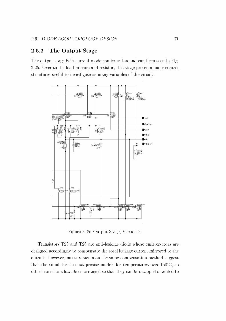
2.5. DIODE LOOP TOPOLOGY DESIGN 71
2.5.3 The Output Stage
The output stage is in current mode conguration and can been seen in Fig.
2.25. Over to the load mirrors and resistor, this stage presents many control
structures useful to investigate as many variables of the circuit.
Figure 2.25: Output Stage, Version 2.
Transistors T23 and T28 are anti-leakage diode whose emitter-areas are
designed accordingly to compensate the total leakage current mirrored to the
output. However, measurements on the same compensation method suggest
that the simulator has not precise models for temperatures over 150°C, so
other transistors have been arranged so that they can be swapped or added to

72 CHAPTER 2. DESIGN
those already present, for proper analysis and tuning. P-channel MOSFETs
M49 and M58 have been sized to supply a constant output current. This is an
optional part that as been added due to the simplicity of adding just another
mirror structure; the result however is function of the trans-conductance
over temperature characteristic, so it will be as precise as the model is. We
also added a structure that aims at compensating the p-channel MOSFETs
leakage. This structure consists in M24, with its VSG = 0, so that the only
current owing to the drain of M17 is its leakage current. This current,
that should be the same for all p-channel MOSFETs (there is the error due
to the slightly dierent reverse bias of each node) is then sunk from all
the vulnerable nodes of the circuit, or just from the output itself if jumper
JMP3 is open (and JMP4 is closed to avoid oating gates). The problems
of mirroring a leakage current are that the mirror structures will introduce
other leakage and that the current involved is very small. If we recall the
formula for a mos drain current, we have
ID =1
2µCox
W
L(VGS − Vth)
2 (2.76)
If ID is very small, VGS is very close to the threshold voltage, that is to say
we have a very small overdrive. This makes the mirror very sensitive to the
Vth mismatch. In order to reduce this sensitivity, we make a WL
= 2µ20µ
to
considerably raise the overdrive. However, the risk that this structure fails is
considered and JMP0 and JMP3 can completely separate this structure from
the output stage. A copy of this current is sunk by resistor R0, so that we
can read the voltage drop it causes and evaluate its magnitude and variation
with reverse bias and temperature. The same thing is done with the NPN
leakage current by T2 and R1. There are also two control structures for the
two PTAT current generated in the PTAT stage.
2.5.4 The Start-up
The PTAT stage, as it has been designed, has also a zero-current operating
point that must be avoided. A start-up circuit that will ensure the correct

2.5. DIODE LOOP TOPOLOGY DESIGN 73
bias point is then required. The start-up implementation is shown in Fig.
2.26. The idea is that the reference voltage VBG is sensed: if it is low or zero,
the bandgap reference is not working, if it is 800mV, it is on and fully working.
Figure 2.26: Start-up stage.
The device performing the voltage-sense must be a mos, because any current
sunk from the output will cause an error. Moreover, the output voltage is set
to be 800mV, that is close to Vth ≈ 0.7V of a standard low voltage n-channel
MOSFET. We than choose to use a digital n-channel MOSFET, who diers
from the low-voltage version also for a lower Vth ≈ 0.5V . Opposite to the
choice taken for the n-channel MOSFET used for the p-channel-MOSFET-
leakage-current compensation, we want this transistor to need little overdrive
to turn it on, so we dimensioned it for high gm with a WL
= 20µ2µ
ratio.
It follows that, when the circuit is o, N2 is sinking no current , there is
then no drop across R70 so VBE,T46 = vcc − vx, (where vx is an unknown
74 CHAPTER 2. DESIGN
value for VBE,T8, although a transient simulation shows VBE,T8 ≈ 250mV ),
so T46 is turned on, injecting current in the error sense node of the loop,
that reacts to compensate the error by lowering VG,mirror so to increase M1
drain-current. This process starts up the circuit. Once the circuit is turned
on, VBG ≈ 800mV causes N2 to sink current from R70. This will turn o
T46 reducing its base voltage while its emitter has risen to the proper bias
point. We aim to have the lower possible VB,T46 voltage (milli-volts) so that
T46 has a negative VBE and is securely turned o. This means that N2
is working in deep triode region. Calculating the pull-up resistor to have
IC,N2 < 1µA, we set R70=4M. We have duplicated this start-up signal also
for the pseudo-supply we have designed to meet the PSRR specication; this
topic will be developed in subsec.s 2.5.5 and 2.5.6.
2.5.5 PSRR
The overall objective of designing a precision reference is to achieve high
accuracy over all working conditions. The term line regulation indicates the
deviation of the reference voltage caused by a variation of the supply. To be
more precise, it indicates the steady state voltage changes in the reference
resulting from DC changes in the supply voltage. The supply voltage can
be also source of transient noise, depending on the environment where the
circuit lies. This noise can be time variant, or can have precise frequency
range where the interference is more severe. This is what is really meant by
PSRR. However, line regulation and PSRR are connected because we can
say that
limf→0
PSRR(f)VDC=K = line regulation|VDC=K (2.77)
This formula means that PSRR tends to the line regulation value for f → 0,
but it also highlights that this is valid only for the DC bias that we are con-
sidering. The pivoting point for improving the PSRR and line regulation is
to decrease the sensibility of sensitive nodes (the reference voltage in par-
ticular) to the input power supply voltage. This concept may be described
assuming a voltage divider from the power supply to the reference voltage
node. Let us take the current-mode output stage of Fig. 2.25. This stage

2.5. DIODE LOOP TOPOLOGY DESIGN 75
can be schematized by the reference part of Fig. 2.27.
Figure 2.27: Pre-regulated pseudo-supply.
The transfer function between Vref and Vpseudo is just the voltage divider
PSRR =∆Vref
∆Vin
=ZGND
ZGND + ZIN
(2.78)
In order to get a high9 PSRR, we need to design little ZGND and high ZIN .
In the current mode output stage, ZGND is the load and is set to be 385kΩ
in our case. ZIN is r0,P , the parallel of the output resistances for all the p-
channel MOSFETs whose drains are connected to the load. This resistance
is
r0 =ηL
ID
(2.79)
where η is a technological parameter. So, being the current imposed to get
the at behavior of the reference voltage over temperature, the only variable
we can play with is the p-channel MOSFET length. This is the limit to the
9PSRR is usually expressed in dB and, being an attenuation is negative: With highPSRR, we are considering the absolute value.

76 CHAPTER 2. DESIGN
PSRR for a current mode bandgap reference. In our case, with L = 25µm,
we have r0 = 225MΩ and we have the parallel of two p-channel MOSFETs,
so ro,P ≈ 140MΩ and Rload = 385kΩ. For these values, we get
PSRRDC = 20 log
(385k
(140M + 385k)
)= −51dB (2.80)
This is a limit that cannot be overtaken without a pre-regulator as shown
in Fig. 2.27. The noisy and variable supply voltage is pre-regulated and
essentially isolated from the reference. Using a pre-regulator, we can write
PSRR =ZPSEUDO−GND
ZPSEUDO−GND + ZPSEUDO−IN
· ZGND
ZGND + ZIN
(2.81)
This way, we can get another −50dB10 from the real supply to VPSEUDO. A
particular attention must however be reserved for the bandgap drive. Lec-
tures as [7] or articles like [10] suggest using diode connected transistor due
to their low impedance in this conguration. This arise two problems:
1. Even supposing IX of Fig. 2.27 being PTAT, the voltage generated
from two diodes supposing their collector current being less than 5µA
will be less than 1V for T ≈ 80°C and it will fall down to 300mV for
T = 180°C, so even stacking three diodes we will leave not enough
headroom for T > 120°C. Diodes and diode-connected BJT are not
suited for our automotive environment11.
2. If using diodes or diode-connected BJT to create the voltage power
supply for the bandgap, the total VPSEUDO variation can go above 1V.
A voltage reference with a normal PSRR of -40dB (100 times attenu-
ation) will show 10mV of total temperature curvature due only to de-
pendence of VPSEUDO from temperature. A temperature compensated
pre-regulator would be better than just a normal one.
10Speaking of DC analysis11Temperature range for automotive products is [-40, 150]°C.

2.5. DIODE LOOP TOPOLOGY DESIGN 77
2.5.6 Pseudo-Supply Design
The basic ideas behind this pre-regulator are
Driving the sub-bandgap reference core circuit by current, supplying
the current needed and reserving a surplus for biasing the ZPSEUDO−GND
impedance and for spare: components mismatch can lower the total
current that the pre-regulator could supply and rise the sub-bandgap
core circuit current consumption.
Exploit the interesting property seen in chapter 1, on Fig. 1.5 on
page 14. This gure shows the existence of VGS for a precise IC that
has low sensitivity to temperature.
We can see the designed circuit in Fig.2.28.
Figure 2.28: Pre-regulator circuit.

78 CHAPTER 2. DESIGN
Being the current needed from the sub-bandgap reference core PTAT in
nature, the rst brick to realize this pre-regulator is the PTAT stage already
seen in this chapter. The RPTAT consists in the series of rph and rpm resis-
tor: their temperature coecient is slightly PTAT for the rpm and CTAT
for the rph. This way, we can modulate the slope of the generated cur-
rent so that, once multiplied for the mirror ratio, it had the same slope of
the current required by the sub-bandgap reference core. However, Monte
Carlo simulation showed that, for low temperatures, a signicant percentage
of samples suered of low supplied current from the pre-regulator. As sus-
pected, components mismatch was moving the bias and, at cold, the current
generated is much less then at hot, so it takes only little mismatch quanti-
ties to reduce the pre-regulator current to the point that the sub-bandgap
core circuit bias is compromised, creating unacceptable behavior. This issue
would be solved increasing the PTAT current generated, but this would have
brought a lot of current to be wasted during from-ambient-to-hot operating
situation. We then thought to implement a circuit that generates a current
boost only at low temperature. This was made by connecting the gate of a
digital n-channel MOSFET to the bases of T3 and T4: this way, the current
sunk by the n-channel MOSFET drain is driven by the base-emitter voltage,
that is (as we know very well at this point) CTAT in nature and decreases
of about -2mV/°C. Vth for the digital n-channel MOSFET is about 500mV,
so when VBE(Tx) ≈ 500mV , the n-channel MOSFET will sink no more cur-
rent, granting no current waste. Last little pearl, being IC proportional to
V 2OV ≈ V 2
BE(T )12, IC is kind of CTAT 2. This and the resistor degenera-
tion give even more precise boost where needed and make it wear o fast
for T > 30°C. This behavior is shown in Fig. 2.29. The start-up for this
stage has been realized exploiting the one already present in the PTAT stage
on the sub-bandgap reference core. If the voltage reference is low, the same
error current injected in the error-sensing node of the PTAT loop is injected
in the pre-regulator loop, starting up the system.
The load of this pre-regulator are two diode-connected n-channel MOS-
FETs. We set the total output current to mach the sub-bandgap reference
12When in saturation region.

2.5. DIODE LOOP TOPOLOGY DESIGN 79
Figure 2.29: Cold current boost.
core current consumption plus about 5µA to bias the two diode-connected
n-channel MOSFETs so that their VGS(T ) matched the point of Fig. 1.5 on
page 14. This way, not only we realized low impedance path to ground, for
improved PSRR, but we also granted a temperature-stabilized voltage for
the sub-bandgap reference core circuit!
2.5.7 AC Stability
Both in PTAT and CTAT stages, collector currents are controlled by loops,
so an AC analysis is required to grant stability and smooth transient re-
sponse. However, the loop bandwidth impact on the ability to reject noise
from supply, hence the PSRR. An overcompensation that will aect the loops
bandwidth will result in a poor PSRRac performance, while low phase mar-
gins compromise in favor of greater bandwidth will cause oscillating transient
response to fast stimuli. The pseudo-supply and the bandgap core shares the
same PTAT stage; however, the compensation for these two stages are dif-
ferent. Let us take a look at the more precise sketch of the PTAT stage for
the pseudo-supply in Fig. 2.30.
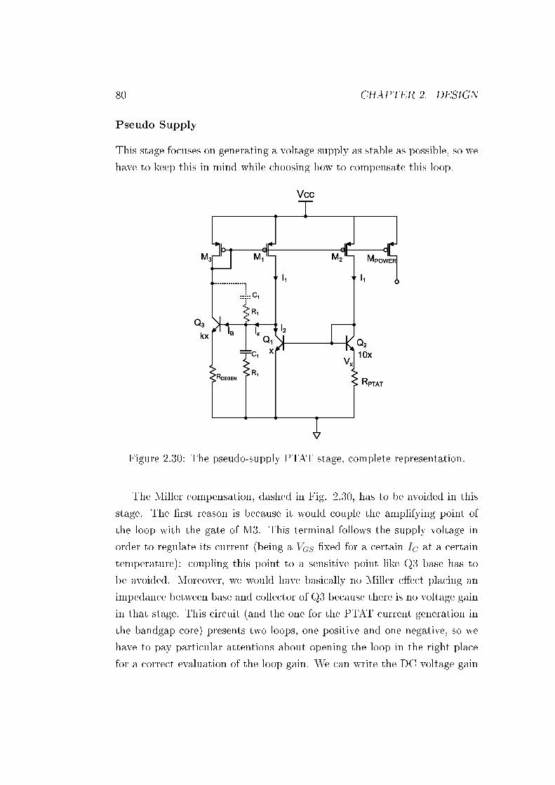
80 CHAPTER 2. DESIGN
Pseudo Supply
This stage focuses on generating a voltage supply as stable as possible, so we
have to keep this in mind while choosing how to compensate this loop.
Figure 2.30: The pseudo-supply PTAT stage, complete representation.
The Miller compensation, dashed in Fig. 2.30, has to be avoided in this
stage. The rst reason is because it would couple the amplifying point of
the loop with the gate of M3. This terminal follows the supply voltage in
order to regulate its current (being a VGS xed for a certain IC at a certain
temperature): coupling this point to a sensitive point like Q3 base has to
be avoided. Moreover, we would have basically no Miller eect placing an
impedance between base and collector of Q3 because there is no voltage gain
in that stage. This circuit (and the one for the PTAT current generation in
the bandgap core) presents two loops, one positive and one negative, so we
have to pay particular attentions about opening the loop in the right place
for a correct evaluation of the loop gain. We can write the DC voltage gain

2.5. DIODE LOOP TOPOLOGY DESIGN 81
for an emitter-degenerated NPN
AV,npn =βRload
rπ + (β + 1)RDEGEN
(2.82)
Being the load a diode connected p-channel MOSFET, Rload = 1gm,M3
. Even
with no degeneration (RDEGEN = 0), AV,npn < 5, so we will have very little
gain for Miller compensation. Note that Miller's eect is function of fre-
quency, because AV (f) is. So it must be carefully applied. Let us write the
block diagram for this loop. We can see it in Fig. 2.31 where
W1(s) =Zcomp
Zcomp + Rin,NPN
(2.83)
is the current divider between the compensation impedance and the input
impedance of Q3 (without loss of generality even if the compensation is not
present, because in that case Zcomp = 1sCP
). We have
Zcomp(s) =sC1R1 + 1
sC1
\\1
sCP
=1
s (CP + C1)· sC1R1 + 1
1 + s(
C1CP
C1+CP
)R1
(2.84)
where CP = Cπ +Av,Q3(f)Cmu and Av,Q3(f) is the voltage gain from the base
to the collector of Q3. Be careful to correctly evaluate CP according to the
frequency.
Rin,NPN = rπ + (β + 1)RDEGEN (2.85)
where again, if no degeneration is applied, RDEGEN can be set equal to zero,
without loss of generality.
W2(s) =r0,M3
1 + gm,M3r0,M3
· 1
1 + sCTOT
(r0,M3
1+gm,M3r0,M3
) (2.86)
W2(s) is the impedance seen from the collector of Q3, that will set the VGS for
the mirrors. CTOT is the total capacitance seen from Q3 collector to ground.
M1 and M2 are identical and share the same bias, so they have the same gm.
However, as already calculated in subsec. 2.4.2 on page 46, there is also the

82 CHAPTER 2. DESIGN
two NPN transistors that work like a current-mirror so we have H1 = 1 and
H2(s) ≈ 3.15 11+sτ
.
Figure 2.31: Pseudo-supply AC-loop block diagram.
We can write the loop gain
T (s) = β ·W1 ·W2 · gm,M1(−3 + 1) (2.87)
= β · 1 + sC1R1
1 + sX + s2 (CP C1R1Rin,NPN)·
· r0,M3
1 + gm,M3r0,M3
· 1
1 + sCTOT
(r0,M3
1+gm,M3r0,M3
) ··gm ·
(−2 ·
1− s τ2
1 + sτ
)(2.88)
where
X = C1R1 + (CP + Cmu) Rin,NPN + C1Rin,NPN (2.89)
If no compensation is applied (both degeneration and C1−R1 series), we get
a DC gain of
|T (0)| ≈ 20 log
(β · 1
gm,M3
· gm · 2)
= 46.4dB (2.90)
and the rst pole is at
fp1 =
[2π · CTOT
(r0,M3
1 + gm,M3r0,M3
)]−1
= 27.5kHz (2.91)
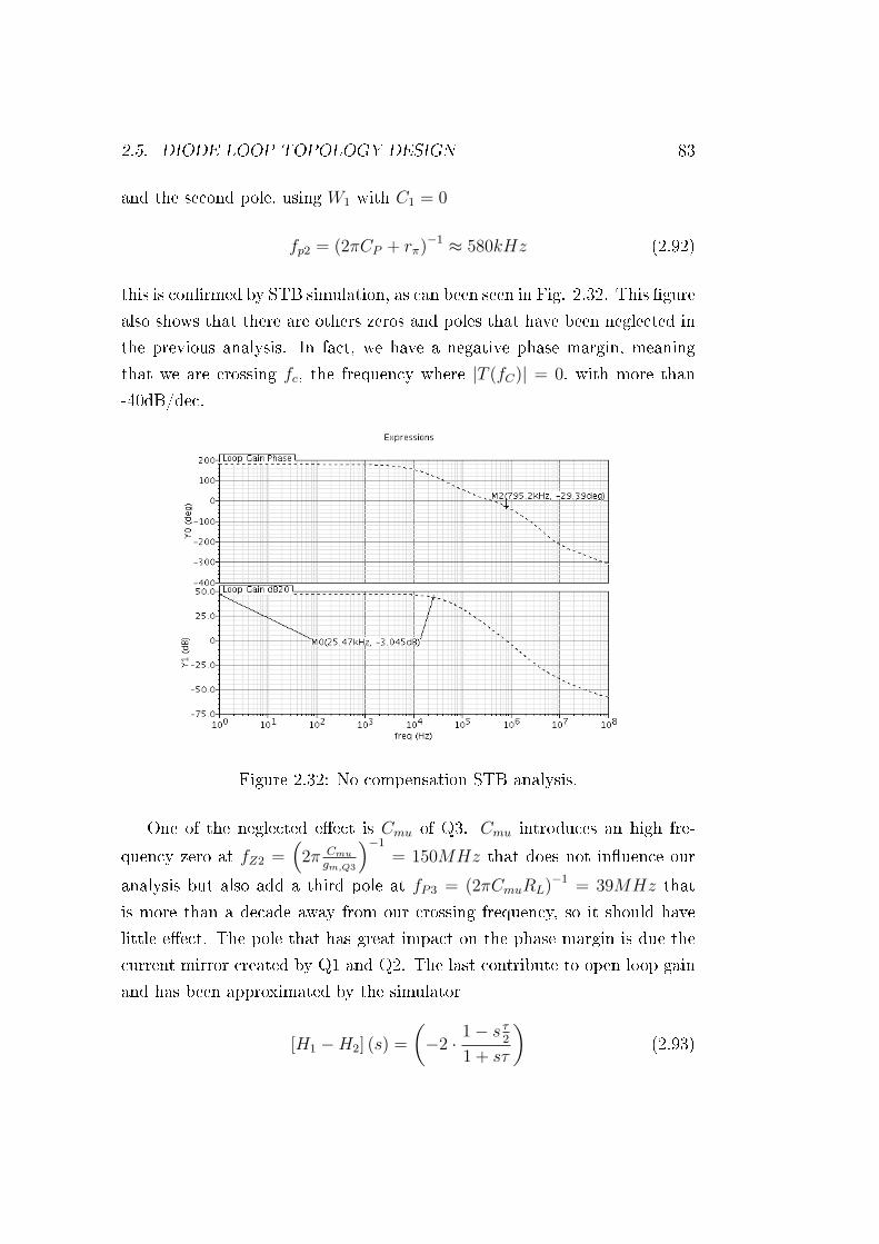
2.5. DIODE LOOP TOPOLOGY DESIGN 83
and the second pole, using W1 with C1 = 0
fp2 = (2πCP + rπ)−1 ≈ 580kHz (2.92)
this is conrmed by STB simulation, as can been seen in Fig. 2.32. This gure
also shows that there are others zeros and poles that have been neglected in
the previous analysis. In fact, we have a negative phase margin, meaning
that we are crossing fc, the frequency where |T (fC)| = 0, with more than
-40dB/dec.
Figure 2.32: No compensation STB analysis.
One of the neglected eect is Cmu of Q3. Cmu introduces an high fre-
quency zero at fZ2 =(2π Cmu
gm,Q3
)−1
= 150MHz that does not inuence our
analysis but also add a third pole at fP3 = (2πCmuRL)−1 = 39MHz that
is more than a decade away from our crossing frequency, so it should have
little eect. The pole that has great impact on the phase margin is due the
current mirror created by Q1 and Q2. The last contribute to open loop gain
and has been approximated by the simulator
[H1 −H2] (s) =
(−2 ·
1− s τ2
1 + sτ
)(2.93)

84 CHAPTER 2. DESIGN
with fPH = 12πτ
≈ 5MHz and so fZH = 10MHz with real part greater then
zero.
Compensation
We will now proceed with the compensation.
Av,Q3 =β
rπ
·W2(s) (2.94)
Av,Q3 has a DC value of 14dB and drops at -20dB/dec rate from about 25kHz,
being W2(s) the input impedance of the load seen by Q3: it follows that one
decade after, at 250kHz, we have no gain, but on the contrary we are already
attenuating, hence no Miller eect. In order to compensate this stage, let
us summarize what poles and zero we have or we can get using degeneration
resistor and C1 −R1 series. In this case we will have
W1(s) = K1·1 + sC1R1
1 + s (C1R1 + CP Rin,NPN + C1Rin,NPN) + s2 (CP C1R1Rin,NPN)(2.95)
W2(s) = K2 ·1
1 + sCTOT
(r0,M3
1+gm,M3r0,M3
) (2.96)
W3(s) = K3 ·1− s τ
2
1 + sτ(2.97)
There are many ways to exploit RDEGEN , C1 and R1 to obtain a compensa-
tion. We aimed for a stable 45° phase margin compensation. With stable we
mean that, if possible, we tried to keep a certain gain margin over a constant
phase. Process and mismatch will cause variations over circuits parameters,
so a phase that is not at at ω = ωc will be more sensitive over circuits
variations. On the contrary, a phase that remains constant over a certain
range of frequency, will be less sensitive to circuit variations. In Fig. 2.33,
gain and phase for this compensation are visible. We used RDEGEN = 100kΩ
and C1 = 5pF to get a dominant pole at fPD = 2, 4kHz and the rst -90°
phase rotation that ends a decade after. At fP1 = 27.5kHz, the second pole
introduced by W2 brings another -20dB/dec and another -90° rotation. This

2.5. DIODE LOOP TOPOLOGY DESIGN 85
way we would approach fc ≈ 150kHz at -40dB/dec, hence PM=0°. We have
still less than one decade before the third pole at fPH = 800kHz and the
rst zero at fZH = 1.6MHz, so these will slightly aect the Bode diagram
at fc and this will be evaluated by simulation. We then decide to play our
negative real part zero just over fc. Being C1 already set to 5pF , we need
R1 =1
2πCfc
= 212kΩ (2.98)
R1has been rounded up to 200kΩ for layout purpose. We veried that our
modeling were congruent with the circuit superimposing the data from ca-
dence to the Bode diagram traced with MATLAB, as shown in Fig. 2.33.
Figure 2.33: MATLAB verication of poles and zeros placement in thepseudo-supply: simulator data are dotted.
This choice for fC gives a phase boost so to cross that frequency with
exactly 45° of phase margin.

86 CHAPTER 2. DESIGN
Bandgap Core, PTAT Stage
The compensation of this part is similar. However, as can be seen in Fig.
2.34, this stage results cascoded by MC and the low impedance DC path
consists in two diode connected n-channel MOSFETs, N1 and N2, in series.
The peculiarity of this stage is that all the AC current sunk from all the p-
channel MOSFETs in the circuit does not come from virtual ground (like in
the pseudo-supply stage, where it was sunk from supply) but from N1 and N2
series, so the low impedance given by those two diode-connected n-channel
MOSFETs works like a source-degeneration. Let us see what we mean.
Figure 2.34: The Bandgap core PTAT stage, complete representation.
Using the notations of Fig. 2.34, we can write that the open loop Av gain
for Q3 is
Av =VC + VB
VA
(2.99)

2.5. DIODE LOOP TOPOLOGY DESIGN 87
We can write VB and VC :
VB =VA
rπ
β
gm,M3
(2.100)
VC = IN ·(
1
gm,N1
+1
gm,N2
)(2.101)
but now IN is
IN = IC,M3 + IC,M1 + IC,M2 + IM,n (2.102)
that is, all the current mirrored by the all the p-channel MOSFETs have to
come from N1 and N2 series. This complicates things a lot since it would be
necessary to evaluate the transfer functionsIM,n
VB. We will do a theoretical
analysis considering the PTAT stage only and we will use some simplica-
tions and the simulator to extend this analysis to the whole circuit; this is
equivalent to say that we are going to analyze IM,n contribution in a second
time. With calculation made from the small signal circuit13 we calculated
the input impedance drawn in Fig. 2.34. It results:
Zin(s) =(1 + kgm,M1RL) + RLgm,M3 + RL
r0
gm,M3
·
·1 + sCT
[r0
r0RL
(1+kgm,M1RL)+gm,M3RL+1
]1 + sCT
[r0
1+gm,M3r0
] (2.103)
where k is a multiplying factor that takes into account the number of p-
channel MOSFETs connected so to share the same VGS of M1 and CT is the
sum of all the CGS connected to the gate of M3. Looking at its DC value,
we get
Zin,DC ≈ RL +(1 + kgm,M1RL)
gm,M3
(2.104)
Using the values of the circuit, we get Zin,DC ≈ 170kΩ, fp ≈ 590kHz and
fz = 1.2MHz . These value are very close to simulation results, but the zero
is at higher frequency. However we only need the bandwidth where Miller
eect can be applied, that is roughly 500kHz. We are now able to evaluate
13See Appendix A.3 on page 130

88 CHAPTER 2. DESIGN
the voltage gain for transistor Q3, assuming that we can use the DC value
for Zin for f < 500kHz.
Av =β
rπ
Zin,DC (2.105)
Substituting the values β and rπ, we get Av = 21.95, that ts with the
Av = 20.7 given by the simulator. Correcting the k factor so to include all
the other p-channel MOSFETs we get Av = 32+AX where AX is the gain due
to the p-channel MOSFET in the CTAT stage. Using the simulator to get
this result by manual verication of Zin(f), we get Av = 34.5. We will exploit
this gain for implementing a Miller compensation. What will follow however
is the compensation of the PTAT stage excluding all the contributes from
other stages of the Bandgap. So our calculation will be done for AV = 20.7.
The open loop gain is given by
T (s) = [W1 ·W2 ·W3] (s) (2.106)
W1(s) = β · 1
1 + s [(Av + 1) Cmu + Cπ] rπ
(2.107)
that is the transfer function Ic
IB(f) for Q3. Then the AC voltage VB (see
Fig. 2.34) pilots the gates of M1 and M2, that transduces this voltage to
collector current by their transconductance gm. So the transfer function
W2 =ID,M1
IC=
ID,M2
ICis given by
W2(s) =gm,M1r0,M3
1 + gm,M3r0,M3
· 1
1 + sCT r0,M3
1+gm,M3r0,M3
(2.108)
which introduces a pole at fp3 = 580kHz and then, like the pseudo-supply,
we have a transfer function due to the mirror made by transistors Q1 and
Q2.
W3(s) = −2 ·1− s τ
2
1 + sτ(2.109)
that introduces a pole at fP,W3 = 5MHz and a zero with real part greater
than zero at fZ,W3 = 2 · fP,W3 = 10MHz.

2.5. DIODE LOOP TOPOLOGY DESIGN 89
Compensation
The compensation is made by introducing an impedance made by resistor-
capacitor in series R1 and C1, so that ZC = 1+sC1R1
sC1R1, as shown in 2.34.
This changes the transfer function W1 because now in the current is di-
vided between the total impedance between base and collector of Q3 and the
impedance between Q3 base and ground. The rst impedance is ZC//Cmu
referred to ground and divided for Av, for f < 500kHz. The impedance seen
from Q3 base is rπ//Cπ. W1C describes the current that ows through rπ
only and so that will be amplied by β.
W1C = β1 + sC1R1
1 + s [C1R1 + A(C1 + Cmu)rπ] + s2[A (C1 + Cmu) rπ
(C1Cmu
C1+Cmu
)R1
](2.110)
with A = (Av + 1) so, writinga = (Av + 1) (C1 + Cmu) rπ
(C1Cmu
C1+Cmu
)R1
b = C1R1 + (Av + 1)(C1 + Cmu)rπ
(2.111)
we can place a dominant pole with R1 = 85kΩ and C1 = 1pF at
fp1 =
[− 1
2π· −b +
√b2 − 4ac
2a
]−1
= 7.8kHz (2.112)
a second pole at
fp2 =
[− 1
2π· −b−
√b2 − 4ac
2a
]−1
≈ 2MHz (2.113)
and the zero at
fz1 = 1.9MHz (2.114)
that almost cancels the second pole. We can say that while the pole at fp1
is correct, the pole at fp2 probably is placed at higher frequency because
the Miller's hypothesis on Av are not valid in that frequency range. The

90 CHAPTER 2. DESIGN
zero,instead, is not inuenced by Miller's eect and so fz1 is reliable. Now
we have to evaluate the transfer functionIC,Q3
IZin. The impedance between
base and collector of Q3 should also be placed between collector and ground
multiplied by Av
1+Av. For f < 500kHz there is no eect on this impedance,
but for f < 500kHz, it tends to zero. For f < 500kHz, we can write:
W2C(s) =1
1 + Zin
Zout,Q3
(2.115)
=
(1 + s CT
gm,M3
)· (1 + sC1R1)
1 + sX1 + s2X2
where X1 = C1R1 + CT
gm,M3+ C1Zin,DC
X2 = CT
gm,M3C1R1 + CT RZC1Zin,DC
(2.116)
and
RZ =r0
r0
RL(1 + kgm,M1RL) + gm,M3RL + 1
(2.117)
This gives two poles at fp3 = 546kHz and fp4 = 678kHz and two zeroes
at fz2 = 587kHz and fz3 = 1.87MHz. While the zero located at fz2 is not
sensitive on Miller's eect, the other two poles and the zero are in a frequency
range where 5 < Av < 20, so 0.83 · Zout,Q3 < Zout,Q3 < 0.95 · Zout,Q3, and
so a slight inaccuracy may aict them. W3C = W2, that remains unaltered
and has a single pole at fp5 = 586kHz and nally we have W4C = W3 with
a pole at fP,W3 = 5MHz and a zero with real part greater than zero at
fZ,W3 = 2 · fP,W3 = 10MHz. The DC gain is then
20Log (|T (0)|) = 20Log
(2β
gm1
gm3
)= 35.6dB (2.118)
The results from simulator have been superimposed to the Bode diagram
drawn with MATLAB and can be seen in Fig. 2.35.

2.5. DIODE LOOP TOPOLOGY DESIGN 91
Figure 2.35: MATLAB verication of poles and zeros placement in the PTATstage: simulator data are dotted.
We have a calculated phase margin of 63° against a simulated value of
77°. However, this analysis excluded part of the circuit. We veried with a
stability analysis that the global circuit does not compromise the stability,
and it results a phase margin of 60°.
Bandgap Core, CTAT Stage
The same approach and similar calculation have been used for the compen-
sation of the CTAT stage, shown in Fig. 2.36.

92 CHAPTER 2. DESIGN
Figure 2.36: The Bandgap core CTAT stage, complete representation.
Let us consider the circuit without the compensation impedance. Consid-
ering a current insertion where marked in Fig.2.36 we can follow the signal
and evaluate its return ratio. The rst transfer function we nd is due to the
current divider at Q1 base node. We have
Zin,Q1(s) =rπ
1 + s [(Av + 1) Cmu + Cπ] rπ
(2.119)
so the current owing on rπwill be
W1,in(s) =RCTAT
rπ + RCTAT
· 1
1 + s [(Av + 1) Cmu + Cπ] RCTAT ·rπ
RCTAT +rπ
(2.120)
that yields a pole at fp1 = 3.5kHz and a Bode gain of 0.2. In order to
calculate this transfer function with had to evaluate the Av gain by the
simulator. This current is then transferred to the output with the transfer

2.5. DIODE LOOP TOPOLOGY DESIGN 93
function
W1,out(s) = β ·[1 + sCmu
(rπ + βRL
β
)](2.121)
introducing a zero at fz1 = 25kHz. This current now ow through Zin,
shown in Fig. 2.36. This impedance yields the transfer function
Zin(s) = 125MΩ · 1
1 + sCgs,M1 (ro,M2 + RL)(2.122)
that transduces the collector current of Q1 to a voltage that drives the gate of
M1, so that its drain current will sink a current proportional to its transcon-
ductance gm,M1. We can write
W2 = Zin · gm,M1 (2.123)
A pole at fp2 = 6kHz is then introduced. This current will be mirrored to
M3 drain with the transfer function
W3(s) =gm,M3r0
1 + gm,M2r0
· 1
1 + sCTr0
1+gm,M2r0
≈ gm,M3
gm,M2
· 1
1 + s CT
gm,M2
(2.124)
where CT is the total capacitance seen from the gate of M2. W3 introduces
a pole at fp3 = 205kHz. The current owing through the drain of M3 will
now see another impedance divider that can be approximated as
W4 =RNL
RNL + RCTAT
≈ 0.3 (2.125)
The total DC gain is the product of all the bode constant of the transfer
function:
Kbode =RCTAT
RCTAT + rπ
· β · 125M · gm,M1 ·gm,M3
gm,M2
· 0.3 (2.126)

94 CHAPTER 2. DESIGN
that expressed in dB, gives
20Log (|Kbode|) = 74dB (2.127)
We can notice that we will cross fc with at less than -40dB/dec, hence no
phase margin. Moreover, we neglected many high frequency poles so the
phase margin will result negative.
Compensation
Let us introduce the compensation impedance consisting in the series of
R1and C1. The transfer function W1,in become
W1,in,C(s) =RCTAT
rπ + RCTAT
· (2.128)
· 1 + sC1R1
1 + s [C1R1 + Av (C1 + Cmu) RP ] + s2 [AvC1CmuRP R1]
Being Av ≈ 60dB, Av heavily boost the compensation impedance (and we
simplied Av +1 ≈ Av), giving a pole at fp1 = 230Hz and a pole-zero cancel-
lation at fp2 ≈ fz1 = 790kHz. We note by the simulator, that even though
Zin,C (Zin compensated) has the expected shape given by a new transfer
function can be calculate as the parallel of Zin the R1−C1 series, the trans-
fer function gm,M1 · Zin is at, with probably some zero-pole cancellations.
W3 remains unaltered with a pole at fp3 = 205kHz and nally the impedance
divider changes in
W4(s) ≈RNL
RNL + RCTAT
· 1 + sAvC1R1
1 + sC1
(AR1RNL
RCTAT +RNL
) (2.129)
which has a zero in fz2 = 530kHz and a pole at fp4 = 2MHz. This zero-pole
placement grants a quasi-constant slope of -20dB/dec from 74dB beginning
at fp1 = 280Hz. That yields, in rst approximation, an fc < fp4, so the
phase margin should be greater than 45°. We calculated with MATLAB
what exact phase margin our zero pole placement yields and veried it with
the simulator. The result is shown in Fig. 2.37.

2.5. DIODE LOOP TOPOLOGY DESIGN 95
Figure 2.37: MATLAB verication of poles and zeros placement in the CTATstage: simulation data are dotted.
The simulator yields a phase margin of 43° versus the 55° of the calculated
value. This imprecision is due also to the high frequency range where fc has
been placed, where simplication hypothesis begins to have a big inuence
on the Bode diagram.
These compensations impact also on transient response and PSRR. An
high phase margin would require a compensation that reduces gain or band-
width greatly, but this would make the loop weaker in rejecting the noise
from the supply, even if guaranteeing a smoother transient response. On the
other hand, a low phase margin would mean higher bandwidth and better
PSRR but overshoot in the output-voltage transient response. This is why
these compensations aim at a compromise between bandwidth and phase
margin of 45°, that should grant a smooth transient response, but still fast
enough to grant a good PSRR.

96 CHAPTER 2. DESIGN
2.5.8 Monte Carlo
The production of wafers involves two typical kind of errors: process and
mismatch. Process errors are related to a phenomenon that aicts all the
same devices in the same way: a shift of resistors nominal values is an ex-
ample. However, the ratio between the process-aicted parameter of the
devices remains constant. Mismatch errors aict the ratio between device
parameters and can cause more severe consequences in this topology. We
will now analyze the main eects that can aict the reference precision. Let
us refer to Fig. 2.38 for the analysis of this subsec..
Figure 2.38: Diode loop topology, explicits circuit.
Resistor mismatch refers to relative dierences in value among resistors
that should nominally have a xed proportion. We can refer the mismatch
of RNL, RCTAT , and RPTAT to Rload for simplicity (Rload constant and all
the other resistors varies all with dierent coecients). We can write new
ratios for these mismatching resistor where α, β and γ are the mismatching
coecient of each resistor (they are all dierent, otherwise we would fall into
a process-kind case). With calculations shown in A.4.1, we determine that
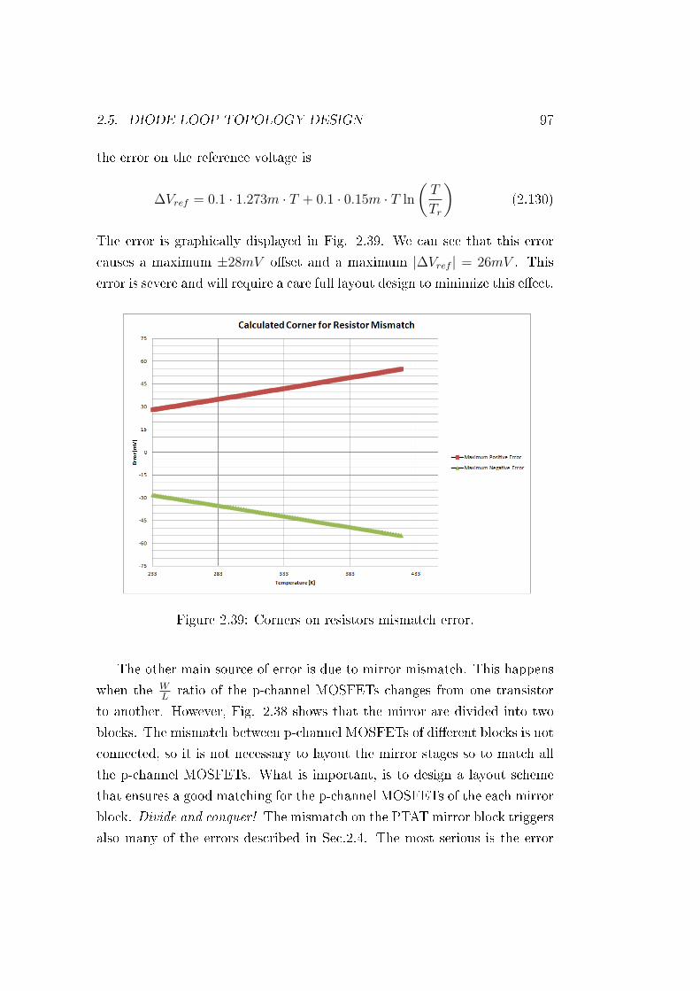
2.5. DIODE LOOP TOPOLOGY DESIGN 97
the error on the reference voltage is
∆Vref = 0.1 · 1.273m · T + 0.1 · 0.15m · T ln
(T
Tr
)(2.130)
The error is graphically displayed in Fig. 2.39. We can see that this error
causes a maximum ±28mV oset and a maximum |∆Vref | = 26mV . This
error is severe and will require a care full layout design to minimize this eect.
Figure 2.39: Corners on resistors mismatch error.
The other main source of error is due to mirror mismatch. This happens
when the WL
ratio of the p-channel MOSFETs changes from one transistor
to another. However, Fig. 2.38 shows that the mirror are divided into two
blocks. The mismatch between p-channel MOSFETs of dierent blocks is not
connected, so it is not necessary to layout the mirror stages so to match all
the p-channel MOSFETs. What is important, is to design a layout scheme
that ensures a good matching for the p-channel MOSFETs of the each mirror
block. Divide and conquer! The mismatch on the PTAT mirror block triggers
also many of the errors described in Sec.2.4. The most serious is the error

98 CHAPTER 2. DESIGN
introduced on the collector-current ratio. Referring to Fig. 2.40, we can
analyze this error using eq. (1.47).
Figure 2.40: PTAT stage, mirror mismatch.
We can rewrite this equation to see the error eect by
IPTAT =VT ln
(αIC1(T )
Ae1JS(T )· Ae2JS(T )
βIC2(T )
)RPTAT
(2.131)
=VT ln (C) + VT ln
(αβ
)RPTAT
(2.132)
so the error introduced is
∆IPTAT =VT
RPTAT
ln
(α
β
)(2.133)
This eect must be superimposed to the eective mirror error. The error is
just the consequence of the modied mirror ratio, so it yields
IPTAT,out =IPTAT
α(2.134)
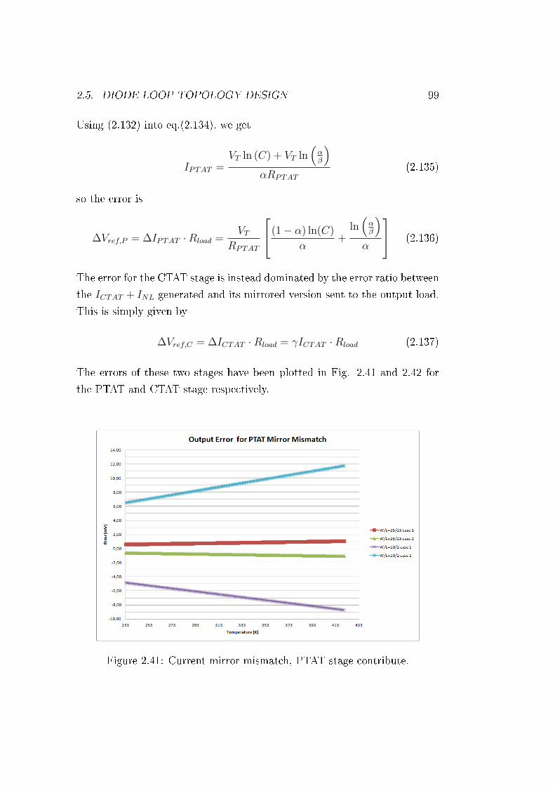
2.5. DIODE LOOP TOPOLOGY DESIGN 99
Using (2.132) into eq.(2.134), we get
IPTAT =VT ln (C) + VT ln
(αβ
)αRPTAT
(2.135)
so the error is
∆Vref,P = ∆IPTAT ·Rload =VT
RPTAT
(1− α) ln(C)
α+
ln(
αβ
)α
(2.136)
The error for the CTAT stage is instead dominated by the error ratio between
the ICTAT + INL generated and its mirrored version sent to the output load.
This is simply given by
∆Vref,C = ∆ICTAT ·Rload = γICTAT ·Rload (2.137)
The errors of these two stages have been plotted in Fig. 2.41 and 2.42 for
the PTAT and CTAT stage respectively.
Figure 2.41: Current mirror mismatch, PTAT stage contribute.

100 CHAPTER 2. DESIGN
Figure 2.42: Current mirror mismatch, CTAT stage contribute.
The PTAT stage presents the interesting characteristic of cancellation
if β > α, this reduces the sensitivity to this stage to mirror mismatching.
Figures 2.41 and 2.42 show also the worst case for two WLratio. These cases
give an idea on how big the p-channel MOSFETs should be sized in order
to obtain certain statistical-precision result and how the error is inuenced
by the area of the transistor.
NPN transistor area can also mismatch, arising an error in the PTAT
generation. This error is however caused by a phenomenon with low variance
and usually lays around δNPN = ±2%. This error cause a ∆Vref,NPN
∆Vref,NPN = VTRload
RPTAT
· ln(1− δNPN) (2.138)
The same calculation can be done for the CTAT stage, where the area ratio
is used to control the non-linear voltage. So, in our case, these errors eect
on Vref in a worst case scenario are shown in Fig. 2.43 and 2.44 respectively.

2.5. DIODE LOOP TOPOLOGY DESIGN 101
Figure 2.43: NPN mismatch, PTAT stage contribute.
Figure 2.44: NPN mismatch, CTAT stage contribute.

102 CHAPTER 2. DESIGN
2.5.9 Extracted Simulation
Once the circuit design has been done and the schematic has been settled,
it is time to perform it layout. Once the layout view is ready, it is possi-
ble to simulate the circuit behavior taking into account parasitic resistances
and capacitors. Thanks to these simulation, we have spotted an anomaly
in the PSRR behavior of version 2. At a glance, the layouts of the three
versions were very similar, but the PSRR at 10kHz for the extracted view
for version 2 was 20dB lower14 than the ideal circuit. This loss was not being
encountered in the other bandgap, so the problem was associated to that
particular layout. This behavior interested only the medium frequency range
and not the DC region, so we simulated the extracted view with only some
well dened range of parasitic capacitors together with all the parasitic resis-
tors. This way, we approximately associated to every parasitic capacitors set
their contribution to the PSRR decrease. Once identied the main source of
degradation, we identied every parasitic capacitors of that set and tried to
see which could contribute to the eect. Following this method, we identi-
ed the main problems: namely the capacitance coupling between sensitive
metal traces and PAD placing. Rerouting some metal paths and changing
the PAD placement (supply and pseudo-supply PAD placed far apart and far
from the output PAD and if possible with the GND PAD between them is a
good solution) brought a big improvement over the PSRR for both medium
and high frequency, of approximately -20dB for 300Hz < f < 10kHz and
-15dB for f > 2MHz, as shown in Fig. 2.45.
14In absolute value.

2.5. DIODE LOOP TOPOLOGY DESIGN 103
Figure 2.45: Improving steps in layout debug.
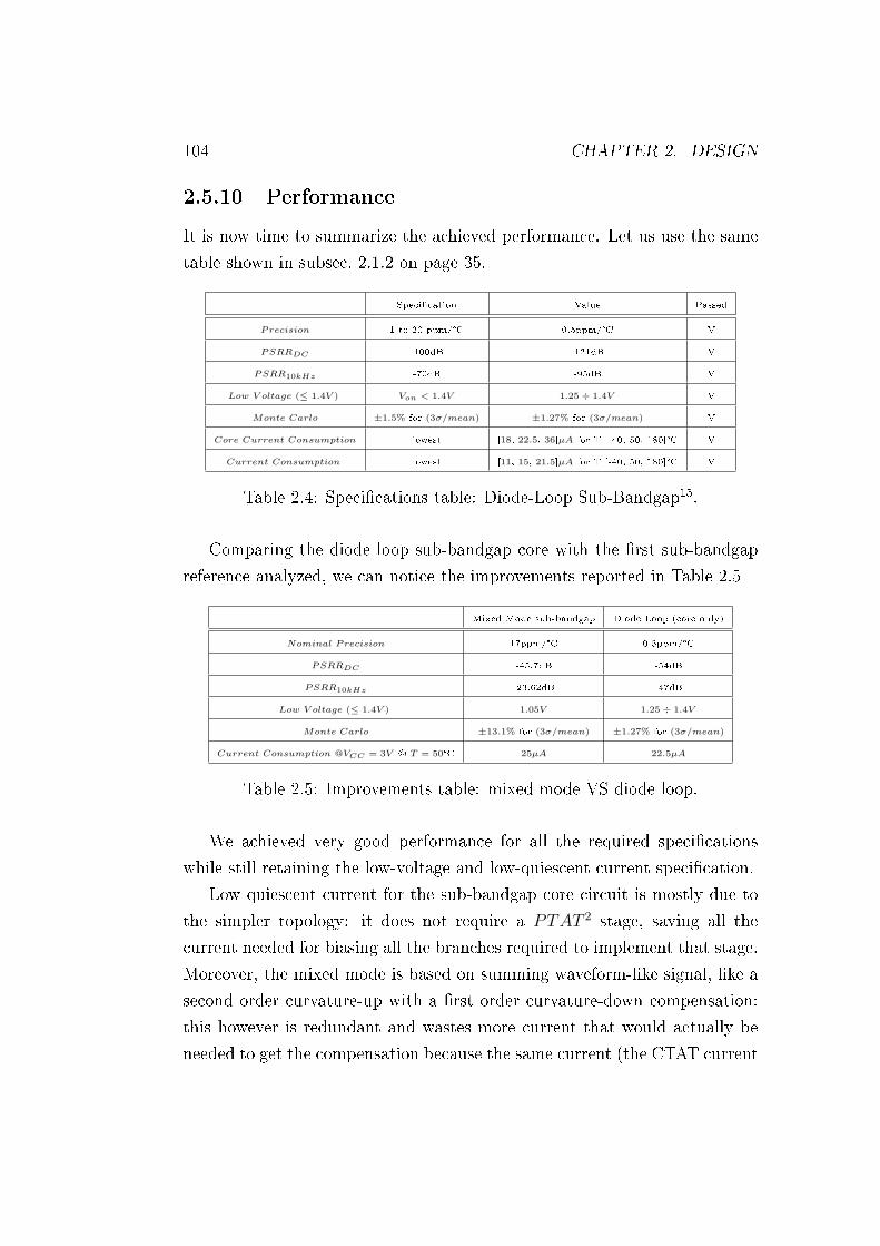
104 CHAPTER 2. DESIGN
2.5.10 Performance
It is now time to summarize the achieved performance. Let us use the same
table shown in subsec. 2.1.2 on page 35.
Specication Value Passed
Precision 1 to 20 ppm/°C 0.5ppm/°C V
PSRRDC -100dB -121dB V
PSRR10kHz -70dB -95dB V
Low V oltage (≤ 1.4V ) Von < 1.4V 1.25÷ 1.4V V
Monte Carlo ±1.5% for (3σ/mean) ±1.27% for (3σ/mean) V
Core Current Consumption lowest [18, 22.5, 36]µA for T [-40, 50, 180]°C V
Current Consumption lowest [11, 15, 21.5]µA for T [-40, 50, 180]°C V
Table 2.4: Specications table: Diode-Loop Sub-Bandgap15.
Comparing the diode loop sub-bandgap core with the rst sub-bandgap
reference analyzed, we can notice the improvements reported in Table 2.5
Mixed Mode sub-bandgap Diode Loop (core only)
Nominal Precision 17ppm/°C 0.5ppm/°C
PSRRDC -45.7dB -54dB
PSRR10kHz -23.62dB -47dB
Low V oltage (≤ 1.4V ) 1.05V 1.25÷ 1.4V
Monte Carlo ±13.1% for (3σ/mean) ±1.27% for (3σ/mean)
Current Consumption @VCC = 3V @ T = 50°C 25µA 22.5µA
Table 2.5: Improvements table: mixed mode VS diode loop.
We achieved very good performance for all the required specications
while still retaining the low-voltage and low-quiescent current specication.
Low quiescent current for the sub-bandgap core circuit is mostly due to
the simpler topology: it does not require a PTAT 2 stage, saving all the
current needed for biasing all the branches required to implement that stage.
Moreover, the mixed mode is based on summing waveform-like signal, like a
second order curvature-up with a rst order curvature-down compensation:
this however is redundant and wastes more current that would actually be
needed to get the compensation because the same current (the CTAT current

2.6. PROPOSED TOPOLOGY IMPROVEMENTS 105
in our second order compensated bandgap) is used twice over dierent loads
to generate the desired curvature compensations. Current mode, on the
contrary, is already compensated before the currents get to the load, and
the load just transduces the current into voltage, so there is no need for
redundant current superposition on dierent loads to get the compensation.
2.6 Proposed Topology Improvements
After the design of the Diode Loop topology, we moved to the re-design of
the proposed second-order compensated sub-bandgap reference. The main
focus of the redesign was to improve the yield of the Monte Carlo statistical
analysis. It is useless to design a second order compensation if the mismatch
errors invalidate the precision that the circuit is capable of. As we saw in
Sec. 2.5.8, resistors and mirrors mismatch are our worst enemy. Resistor
mismatch can be counteracted by layout solutions, that are more eective
if the resistors value are easy to recreate with series or parallel of the same
resistor-module. This allows an inter-digitation layout of resistors and their
placement in the same area of the circuit, improving matching. Big p-channel
MOSFET mirrors also improve matching, and reduce Early eect at the same
time. The AC compensation must now be tuned on the new capacitance
introduced by the bigger p-channel MOSFETs and the whole circuit must be
tuned to compensate the changes in errors like dierent base currents and
Early eects. The result of this redesign is shown in Table 2.6.
First Design sub-bandgap Second design sub-bandgap
Nominal Precision 17ppm/°C 4ppm/°C
PSRRDC -45.7dB -45.7dB
PSRR10kHz -23.62dB -23.6dB
Low V oltage (≤ 1.4V ) 1.05V 1.05V
Monte Carlo ±13.1% for (3σ/media) ±1.7% for (3σ/media)
Current Consumption @VCC = 3V @ T = 50°C 25µA 20µA
Table 2.6: Improvements table: rst VS second design.
The most important improvement can be seen in the statistical analysis,

106 CHAPTER 2. DESIGN
where the error signicantly reduced from 13.1% to 1.7%. The error correc-
tion brought also a signicant improvements over the nominal precision of
the temperature coecient of the reference voltage and a -20% current con-
sumption at ambient. The drawback is a larger area for the whole bandgap
reference circuit, that increased of 35%.

Chapter 3
Measurements Vs Simulations
This chapter will discuss the measurements we collected for three test-chip
samples, each one holding two of the second-order curvature-corrected bandgap
reference, pre-redesign version seen in chapter 2. These measurements will
then be compared to the nominal and statistical values expected in order to
investigate if the statistical model predictions are respected and to check if
the implementation of the solution to the leakage problem worked correctly.
3.1 Analyzed Topologies and Procedures
The two circuits tested in these three test-chip samples are substantially the
same circuit showed in 2.1 on page 29. What makes them dierent is the
presence (LGK version) or less (SBG) of a leakage compensation in the
PTAT stage, highlighted in Fig. 3.1. The measurement sets and procedures
are the following:
Set 1
This set of measurements aims at evaluating the precision of the voltage
reference, the current consumption and indirectly the line regulation. It
consists in two measurements:
Connecting the circuit as shown in Fig. 3.2.
107

108 CHAPTER 3. MEASUREMENTS VS SIMULATIONS
Figure 3.1: Leakage compensation structure.
Output voltage (that we will call VBG) at four dierent input voltages
[1.5, 2, 3, 4]V from -40°C to 180°C, with steps of 10°C.
Input current (that we will call Iin) at four dierent input voltages:
[1.5, 2, 3, 4]V from -40°C to 180°C, with steps of 10°C.
Figure 3.2: Connections setup for Set 1.

3.1. ANALYZED TOPOLOGIES AND PROCEDURES 109
Set 2
This set exploits the availability of the output pin and the low impedance
output stage to measure the value of the resistor ladder (that is the series of
the three resistors used for the mixed mode output) of this stage. This will
bring a direct comparison between measured resistances and their nominal
value. The measure consists in:
Connecting the circuit as shown in Fig. 3.3
Measurement of VBG while sinking Itest = 100µA from VBG pin as
shown in Fig. 3.4 to avoid turning on the anti-parallel diodes of the
p-channel MOSFET mirrors.
Measurement of VBG while sinking Itest = 300µA from VBG pin to check
that this measurement is not bias-depending.
Figure 3.3: Connections setup for Set 2.
Set 1 will be used for measurements of the output voltage also after two FIB1
modication. The modications will be called FIB1 and FIB2.
FIB1
FIB1 is a cut FIB that disengage the whole compensation stage from the rest
of the circuit. Fig. 3.5 shows a picture taken from the microscope.
1Focused Ion Beam.

110 CHAPTER 3. MEASUREMENTS VS SIMULATIONS
Figure 3.4: Connections setup for Set 2, inside view.
Figure 3.5: FIB cut: microscope picture.
FIB2
FIB2 is a FIB that reconnects 2 NPN transistor of Ae = 2 in anti-leakage
conguration to the output net of the circuit. The idea, as explained in

3.2. MEASUREMENTS VS SIMULATION 111
chapter 2, is to sink the excess of current mirrored to the load due to leakage
errors all over the circuits before it reaches the load itself. This solution is not
precise, because there is no connection between the error current and this
sunk current, other than they are consequences of the same phenomenon.
However, for a certain input voltage and transistor in anti-leakage congura-
tion connected to the load, we can have a good reduction of the VBG error.
We will now compare the measurements taken and see if they are inside the
statistical range foreseen by the simulator.
3.2 Measurements VS Simulation
3.2.1 Voltage Reference and Current Consumption
Because we are eager to know if our sub-bandgap reference is precise or not,
we will evaluate the results that comes from Set 1. Results are shown in
Fig. 3.6, where SBG and LGK version are compared to the same corner,
being practically the same circuit. We can see that one of the six voltages
Figure 3.6: VBG measurements VS VBG corner values.
measured is border-line with the lower corner and one is even out of the cor-

112 CHAPTER 3. MEASUREMENTS VS SIMULATIONS
ner range. Also the input current sees a little shift towards the upper region
of the region of the statistical foreseen values. This is shown in Fig. 3.7. This
Figure 3.7: Iin measurements VS Iin corner values.
can nd an explanation by measurements done with Set 2, that has shown a
very severe process variation on the output resistance. Fig. 3.8 shows a -20%
process variation for this resistance (series). These measurements moves ac-
cordingly to the analysis shown in Sec. 2.5.8 on page 96: short channel length
and resistor mismatches actually have a big impact on the precision of this
voltage reference to the point that the eorts for developing a second order
compensation are wasted. So we have a bad compromise between area and
precision and power consumption and precision. For instance, a rst order
sub-bandgap reference with longer channel length and less components would
probably have had better performance, needing less area and less power. It
is important to remember that a 25µmx25µm p-channel MOSFET is still
2.5 times smaller than a NPN with Ae = 1 in this technology, so saving a
total of 5 Ae (that is the total area occupied only by the NPN necessary for
implementing the PTAT 2 stage) we would be able to use just about half of
that area for all the 25µmx25µm p-channel MOSFETs needed to implement
a rst order current mode sub-bandgap reference, that would show higher
precision.

3.2. MEASUREMENTS VS SIMULATION 113
Figure 3.8: Output resistance measurement Vs nominal value.
3.2.2 Line Regulation
It is also possible to evaluate an approximate estimation for the line regula-
tion: adapting eq. (1.3) for a discrete case, we have
PSRRDC(VIN) =∆VOUT (VIN)
∆VIN
(3.1)
Applying this formula to the measurements taken we get the values reported
in Tab. 3.1: These values are in line with those reported by the simulator.
@VCC Sample 1 Sample 2 Sample 3
1.75V -45.5dB -46dB -44.5dB2.5V -43.1dB -44.4dB -43.1dB3.5V -43dB -44.4dB -43.1dB
Table 3.1: Line regulation estimation.
3.2.3 Leakage
Some very interesting observation can be extrapolated from the FIB mea-
surement about the leakage currents. Fig. 3.9 resumes all the measurements
done and will come in handy to get the analysis easier. FIB1 is indicated as

114 CHAPTER 3. MEASUREMENTS VS SIMULATIONS
Post FIB and FIB2 as Post Connection FIB. At rst glance, the FIB2
shows the most eective compensation, and is the less sensitive to sup-
ply variations, with a ∆VBG,FIB2 = 0.74 − 0.7 − DCshift ≈ 32mV versus
∆VBG,FIB2 = 0.780 − 0.715 − DCshift ≈ 58mV , where DCshift considers
the eect of line regulation. The leakage compensation shown in 3.1 is in-
eective for VCC > 2V . Despite the fact that the current ILC sunk by the
compensation stage generate a negative ∆VPTAT
∆VPTAT = ln
(1− ILC
IC2
)(3.2)
and, due to the loop in the PTAT stage, a proportional current is also sub-
tracted to the total output load, this strategy does not work. There is no
circuital reason for this eect to take place because, even if this tempera-
ture range could make transistor work in a week operative point (such as
low VCE). One of our guess is that a PAD lying very close to one of the
NPN anti-leakage transistor, being connected to an high voltage net, turns
on a parasitic structure. Acting like a gate for a parasitic MOSFET, it could
slightly turn on this parasitic device in a weak-inversion operating mode.
This would explain the current injected that counteracts the compensation.
FIB2 directly sinks current from the total output current, re-absorbing part
of the current introducing by leaking junctions. From this measurement, we
could do an interesting evaluation. Let us consider the dierence between
the value of VBG for FIB2 and for VBG with no compensation applied and let
us call it ∆VBG,F : considering VBG constant when biasing the anti-leakage
NPN in FIB2, they will sink always the same current IL,FIB2, no matter at
what voltage the power supply is. What we expect is that, for a xed tem-
perature, the contribute ∆VBG,F remains constant, but this is not what it is
happening. In fact, we can see a variation over ∆VBG,F . Let us take a look
at Tab. 3.2. Knowing the output resistance and its temperature dependence,
we can plot the current ILC for each supply voltage, and comparing it with
the current calculated by the simulator. The results are shown in Fig. 3.10.
We can see a big discrepancy between the simulated model and the measured
one, and this will cause the eects of leaking current all over the circuit to be

3.2. MEASUREMENTS VS SIMULATION 115
Figure 3.9: FIB measurements.

116 CHAPTER 3. MEASUREMENTS VS SIMULATIONS
Temp [°C] ∆VBG,F @ VCC = 4V [mV ] ∆VBG,F @ VCC = 3V [mV ] ∆VBG,F @ VCC = 2V [mV ]
180 17,37 18.34 18.96
170 8,42 8.92 9.28
160 3,99 4.12 4.23
150 1,91 1.87 1.796
140 0,90 0.82 0.72
130 0,59 0.51 0.451
120 0,07 0.05 0
Table 3.2: VBG variation between no compensation and FIB2 modication.
Figure 3.10: Leakage current: measurements VS simulation.
dicult to predict. The small changes between the dierent values for ILC at
dierent supply voltages can be due to the slightly dierent bias that both
the NPN in anti-leakage conguration and the p-channel MOSFETs of the
mirror are subjected to. Down to this values, Early voltage and instrument
limits bring non-negligible errors.

Chapter 4
Discussion And Comparison With
Other Topologies
In this chapter, we will summarize the results we achieved with this design,
and we will compare them with other topologies developed at Inneon Tech-
nologies.
4.1 Main Objectives
Our purpose was to study the implementation of a sub-bandgap voltage ref-
erence that fullls very strict specications. The rst important choice is
of course the topology, that must be chosen to be the one that suits the
specication best. Before starting any implementation (or re-design) activ-
ity, silicon physic has been evaluated and all the main sources of errors in
the sub-circuits that will constitute the whole project have been analyzed.
This pre-evaluation allowed to be aware of the causes of certain eects and
to prevent or mitigate them eectively. The result seems very promising,
with an astonishing nominal precision, a very robust behavior to process and
mismatch deviations, ultra-low voltage and excellent PSRR and Line Regu-
lation performances. However, an electronic designer knows that all comes
at a price, and if no trade o are accepted, some parameters will then take
on their shoulders all the weight of our choices, most of the time area and
117

118CHAPTER 4. DISCUSSION AND COMPARISONWITHOTHER TOPOLOGIES
Compensation Output Stage Pre-regulated Supply Sub-bandgap
Bg1 Exact Current-Mode Yes Yes
Bg2 First Order Voltage-Mode Yes No
Bg3 Second Order Mixed-Mode No Yes
Bg4 First Order Current-Mode No Yes
Table 4.1: Analyzed structures.
current consumption. So, assumed that excellent design has been performed,
some topologies will just perform better in some elds than others. This
is why we think it is useful to compare dierent bandgap and sub-bandgap
structures, so to understand what their capabilities are.
4.2 Final Comparison and Evaluation
We have compared our developed projects to other voltage references. The
analyzed topologies are reported in Tab. 4.1. These topologies have been
chosen because they represent the widest combination of dierent possibilities
available.
Bg1 refers to the pre-regulated current mode sub-bandgap voltage ref-
erence designed in this thesis.
Bg2 is a pre-regulated voltage-mode bandgap reference already devel-
oped by Inneon DC ATV STD VREG team.
Bg3 is the proposed mixed-mode circuit before the re-design process.
Bg4 is another sub-bandgap we designed using the same concept used
for Bg1, with the dierence that is it is rst-order compensated and
that it is designed for very low quiescent current.
Fig. 4.1 shows where each one performs best and is commented in subsec.
4.2.1 and 4.2.2.

4.2. FINAL COMPARISON AND EVALUATION 119
Figure 4.1: Performances comparison.

120CHAPTER 4. DISCUSSION AND COMPARISONWITHOTHER TOPOLOGIES
4.2.1 PSRR and Transient Response
Transient response shows the turn on of the circuits with a 10µs slope from
0V to 3V of the supply voltage. PSRR1 values have been taken for a supply
voltage of 3V, so all the circuits are in their optimal working bias condition.
In this condition, the pre-regulated voltage references have a -75dB boost in
the quasi-DC frequency range and then the frequency behavior is dependent
on how the compensation is done and what structures implements the voltage
reference. We can see that Bg1 is scoring about -27dB against the other
pre-regulated circuit at f = 10kHz, while the non pre-regulated bandgap
references dier because of dierent compensation choices: Bg3 has a more
aggressive AC compensation, meaning more phase margin and less bandwidth
where Bg4 has less phase margin but more bandwidth. This reects on the
transient response, that shows much more overshoot for Bg4 and a slower but
smoother response for Bg3. Pre-regulated supply shows slower response to
power-supply turn on, due mostly to the turn on of the power stage (because
of the big gate capacitance associated). Bg2 has a similar structure as Bg1,
with smaller power stage, so the reference voltage raise faster and in two
dierent times, but the total amount of time taken is still little greater then
Bg1.
4.2.2 Line Regulation and Start-Up
Line regulation shows three distinct zones where each voltage reference works
best. The pre-regulated references have better line regulation when also
the power supply is turned completely on. If the cascoding stages or the
p-channel MOSFETs constituting the mirrors of the bandgap core circuit
are not in saturation region, their output resistance drops abruptly and,
as shown in subsec. 2.5.5 on page 74, the PSRR drops too. For a supply
voltage lower than 1.5V, non pre-regulated references have better PSRR and
line regulation, and this threshold must but moved about 300mV higher if
considering operation at cold (-40°C), because of the higher VBE(T ) oset.
1The measurements where performed with 1pF of external capacitance connected be-tween VBG and ground.

4.2. FINAL COMPARISON AND EVALUATION 121
After that threshold, pre-regulated voltage regulator have up to -90dB better
performance, depending on the pseudo-supply and the bandgap core circuit
implementation. Bg1, having a current-mode low-voltage output stage, even
if pre-regulated, has minimum voltage of about 1.4V against the 2.3V of Bg2,
which features a voltage-mode output stage. Bg1 has practically a minimum
voltage that is one overdrive higher than that required for a current-mode or
mixed-mode reference.
4.2.3 Nominal Precision and Statistical Analysis
One of the most important tasks for a voltage reference is precision. This is
why we struggle for second order compensation, fancy curvature compensa-
tion and exact compensation, and every compensation has its impact in terms
of area and power consumption. The physical implementation of the chip has
the most crucial impact over the performance of the circuit and could impair
all the benet of the most complex compensation. This is also why bandgap
references are usually trimmable, but this operation can be risky and will
add additional costs. We will analyze dierent implementation methods to
see what are their benets and their drawback. Fig. 4.2 shows the nominal
output voltages for the four examined voltage references. The temperature
range stops at 120°C to avoid dragging leakage eects into this evaluation.
Bg1 is designed to hit the best compensation possible: in fact, the topol-
ogy that has been chosen exploits an exact compensation method and an
extensive errors prevention and correction has been applied. However, in the
layout phase, not all resistors where proportional and easy to be layouted
with combinations of resistor modules; however, the modularity has been
reached, but at the cost of more area usage. Bg2 has been designed to accept
the compromise of a slightly sloped output, but retains easy matching for re-
sistors, that have been layouted easily; moreover, the pre-regulator and the
bandgap core circuit have been designed to optimize the area, without the
need (like for Bg1), of a real power stage. Bg2 is implemented in voltage
mode, and its precision is strongly depending on resistor matching, while
current and mixed-mode needs also an accurate mirror matching. Bg3 is

122CHAPTER 4. DISCUSSION AND COMPARISONWITHOTHER TOPOLOGIES
Figure 4.2: Nominal output voltage.
also set for high accuracy, but has been designed for low area usage (minimal
length p-channel MOSFETs!). Bg4 is set for maximum precision (for a rst
order bandgap reference) and minimum current consumption; due to the low
area required for its implementation and to mitigate the errors introduced
by such a low current usage (Icc@3V < 6µA, T=25°C), mirrors are sized
for high matching precision. We will now cross in Tab. 4.22 the simulated
results for nominal output voltage, current consumption, area and statistical
analysis to make some interesting considerations...
TCref [ppm] Statistical Precisionh
3σµ
%i
Areaˆmm2
˜Current @ VCC = 3V
Bg1 0.55 ±1.5% 0.14 (a) - 0.24 (b) 13 (a) - 20.5 (b)
Bg2 19 ±1.73% 0.13 12
Bg3 10.4 ±10% 0.07 21.5
Bg4 12 ±1.72% 0.06 5.5
Table 4.2: Precision, area and current consumption performance.
2(a) and (b) refers respectively to pseudo-supply disengaged or engaged. Current con-sumption is evaluated at T=25°C
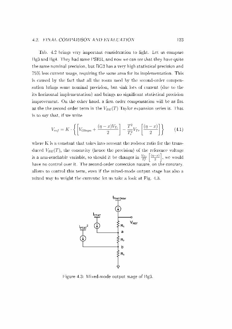
4.2. FINAL COMPARISON AND EVALUATION 123
Tab. 4.2 brings very important consideration to light. Let us compare
Bg3 and Bg4. They had same PSRR, and now we can see that they have quite
the same nominal precision, but BG3 has a very high statistical precision and
75% less current usage, requiring the same area for its implementation. This
is caused by the fact that all the room used by the second-order compen-
sation brings some nominal precision, but sink lots of current (due to the
its horizontal implementation) and brings no signicant statistical precision
improvement. On the other hand, a rst order compensation will be as at
as the the second order term in the VBE(T ) Taylor expansion series is. That
is to say that, if we write
Vref = K ·[
VG0npn +(η − x)VTr
2
]− T 2
T 2r
VTr
[(η − x)
2
](4.1)
where K is a constant that takes into account the resistor ratio for the trans-
duced VBE(T ), the concavity (hence the precision) of the reference voltage
is a non-reachable variable, so should it be changes in VTr
T 2r
[(η−x)
2
], we would
have no control over it. The second-order correction nature, on the contrary,
allows to control this term, even if the mixed-mode output stage has also a
mixed way to weight the currents: let us take a look at Fig. 4.3.
Figure 4.3: Mixed-mode output stage of Bg3.

124CHAPTER 4. DISCUSSION AND COMPARISONWITHOTHER TOPOLOGIES
We can see that changing R3 (that is usually much smaller than R1 and
R2) we will alter Vb, but also slightly3 modify Va and of course Vref , un-
balancing how the three currents are translated into voltages and how this
voltages are summed, not just the Vb component.
3Slightly because R3R2
< 1 and R3R1 1 so, being the total impedance where Ifirst order
and ICTAT ow is respectively (R1 + R2 + R3) and (R2 + R3), R3 changes have dierentimpacts on the other two voltage components depending on the weight of R3 on the totalimpedance.

Chapter 5
Conclusions
This work focused on studying the dierent implementations of sub-bandgap
structures and all the related source of errors, both systematic and random.
Our investigation began from silicon physical properties, went through the
solution of many analog problems and analyzed how to reduce the impact
of statistical events (like components mismatch) over the specication of
reliability and precision we aimed to achieve. With all these knowledge, it was
possible to design a new structure that aims at representing a state-of-the-art
device between the ultra-low voltage references. However, no structure will
be denitive: as we showed in chapter 4, every structure has its strength
and weakness, and it should be chosen accordingly to the system into which
it will work. Our hope however is that this work could have shown how to
deal with the many problematics related to the implementation of a high
performance ultra-low voltage sub-bandgap circuit and be itself a reference
and an instrument for any engineer who needs to design one.
125

126 CHAPTER 5. CONCLUSIONS

Appendix A
Appendix
A.1 Base Emitter Voltage Calculation
A.1.1 General VBE(T ) expression
VBE(T ) = kTq
ln(
Ic(T )IS(T )
)(1)
VBE(Tr) = kTr
qln(
Ic(Tr)IS(Tr)
)(2)
(A.1)
Tr · VBE(T ) = kTq
ln(
Ic(T )IS(T )
)· Tr (1)
T · VBE(Tr) = kTr
qln(
Ic(Tr)IS(Tr)
)· T (2)
(A.2)
Now, subtracting eq(1) and eq(2) leads to
VBE(T ) =T
Tr
VBE(Tr) +kTTr
qTr
ln
(Ic(T )
IS(T )
)− kTTr
qTr
ln
(Ic(Tr)
IS(Tr)
)(A.3)
=
(T
Tr
)VBE(Tr) +
kTr
q
[ln
(IS(Tr)
IS(T )
IC(T )
IC(Tr)
)](A.4)
127

128 APPENDIX A. APPENDIX
A.1.2 Precise VBE(T ) calculation
Expliciting all temperature-related parameters in 1.9 on page 7 lead to
IS(Tr)
IS(T )=
BT 3r exp
(−qVG(Tr)
kTr
)· D(Tr)
BT 3 exp(−qVG(T )
kT
)· D(T )
=T 3
r exp(−qVG(Tr)
kTr
)· VTr · CT−n
r
T 3 exp(−qVG(T )
kT
)· VT · CT−n
=T
(4−n)r exp
(−qVG(Tr)
kTr
)T (4−n) exp
(−qVG(T )
kT
) (A.5)
then, for η = 4− n
ln
(IS(Tr)
IS(T )
)= ln
[(T
Tr
)η]+ ln
exp(−qVG0(Tr)
kTr
)exp
(−qVG0(T )
kT
)
= η ln
(Tr
T
)+ ln
[exp
(VG0(T )
VT
− VG0(Tr)
VTr
)]= −η ln
(T
Tr
)+
VG0(T )
VT
− VG0(Tr)
VTr
(A.6)
Using (A.6) in (A.4) we get
VBE(T ) =T
Tr
· VBE(Tr) +T
Tr
VTr
(−η ln
(T
Tr
)+
VG(T )
VT
− VG(Tr)
VTr
)+
T
Tr
VTr ln
(IC(T )
IC(Tr)
)=
T
Tr
· VBE(Tr)− VT η ln
(T
Tr
)+ VG(T )− T
Tr
VG(Tr)
+VT ln
(IC(T )
IC(Tr)
)(A.7)

A.2. LINEAR REGUALTOR ANALYSIS 129
A.2 Linear Regualtor Analysis
A.2.1 Block Diagram of LDO Linear Regulator
This is the explicit calculation for the Block diagram seen in Fig. 1.12 on
page 25:
[(VOH − LVin) A + VinMB + VinC] (−P ) + VinQ = VO
−VOHPA + LPAVin − VinMBP − VinCP + VinQ = VO (A.8)
Vin [LPA−MBP − CP + Q] = VO(1 + HPA) (A.9)
so we getVO
Vin
=P (LA−MB − C) + Q
1 + HPA(A.10)
A.2.2 PTAT W transfer function calculation
In Fig. A.1 is reported the small signal equivalent model for the NPN couple
of the PTAT stage.
Figure A.1: NPN mirror eect, small signal schematic.
We can write
IT = β1IB1 + IB1 + IB2 = (β1 + 1)IB1 + IB2 (A.11)
IPTAT = (β1 + 1)IB1 (A.12)
IB2 =((β1 + 1)IB1RPTAT + IB1rb,1)
rb,2
(A.13)

130 APPENDIX A. APPENDIX
Using (A.13) in (A.12), we get
IB2 = (IT − IB) · RPTAT
rb,2
+(IT − IB)
(β1 + 1)· rb,1
rb,2
(A.14)
IB2
(1 +
RPTAT
rb,2
+rb,1
rb,2(β1 + 1)
)= IT
(RPTAT
rb,2
+rb,1
rb,2(β1 + 1)
)(A.15)
Substituing the values from spectre operative point, we get
β2IB2
IT
≈ Iout
IT
= 3.15 (A.16)
A.3 AC Stability
The use of a pseudo-supply introduces some complications in the AC analysis
of the bandgap core stages. We are then going to do an explicit evaluation of
the impedance seen from Q3 collector of Fig. 2.34 on page 86 as an example
of how to handle the analysis when a pre-regulator like our pseudo-supply is
used. In fact, not all the transfer functions will be explictly evaluated, as this
is not the purpose of this thesis. However, we think that it should be usefull
to see just this calculation, being slightly dierent from what we usually run
into.
This analysis will consider only the p-channel MOSFETs responsible for
the PTAT-current generation-loop, and is extandable to any structure with
other pmos that share the same VGS. In this case, the small signal model-
lization for the circuit is shown in Fig. A.2. The k indicates an eventual
multiplier equivalent to the number of identical pmos added for mirroring
purpouse. If they are not identical, gm,TOT will just be the sum of the dif-
ferent gm. The same for the output resistor: if they are dierent, manual
calculation for the total impdence must be done.

A.3. AC STABILITY 131
Figure A.2: Small signal circuit for cascoded PTAT stage AC analysis.
Using the notations of Fig. A.2, we can write the following couple of
equations VA = [IT + (VT − VA) kgm,M1] RL (a)
(VT − VA)(
1Z0
+ 1gm,M3
)= IT (b)
(A.17)
where Z0 =r0,M3
1+sCT r0,M3. Solving eq. (A.17)(a) for VA, we get
VA =IT RL + VT · kgm,M1RL
(1 + kgm,M1RL)(A.18)
Now we can solve eq. (A.17)(b). After some calculation, we get
VT
IT
= Zin(f) =Z0 (1 + kgm,M1RL)
1 + gm,M3Z0
+ RL (A.19)
We can immediatly see its DC impendance, being Z0 = r0, we get
Zin,DC = RL +(1 + kgm,M1RL)
gm,M3
(A.20)
Explicitng Z0 we get
Zin(f) =(1 + kgm,M1RL) + RLgm,M3 + RL
r0
gm,M3
·1 + sCT
[r0
r0RL
(1+kgm,M1RL)+gm,M3r0+1
]1 + sCT
[r0
1+gm,M3r0
](A.21)

132 APPENDIX A. APPENDIX
A.4 Monte Carlo
A.4.1 Resistors Mismatch
Refering the mismatch of RNL, RCTAT , and RPTAT to Rload, we can write
new ratios for these mismatchig resistorsαRload
RPTAT
βRload
RCTAT
γRload
RNL
(A.22)
where α, β and γ are the mismatching coecients of each resistor (they are
all dierent, otherwise we would fall into a process-kind case). The resistors
are dimensioned so that
V ref = VGO,npn +
(Rload
RPTAT
k1 −Rload
RCTAT
k2
)T + (A.23)
+
(Rload
RNL
k3 −Rload
RCTAT
k4
)T ln
(T
Tr
)(A.24)
≈ VGO,npn (A.25)
where kx are process and temperature indipendent constant. This means
that Rload
RPTATk1 = Rload
RCTATk2 = x
Rload
RNLk3 = Rload
RCTATk4 = y
(A.26)
Combining eq. (A.22) and (A.26) in (A.23), we get
V ref = VGO,npn + x (α− β) T + y (γ − β) T ln
(T
Tr
)(A.27)
No mismatch would imply α = β = γ. Mismatching variations percent are
usually beetwen 0.1 and 5%. Assuming the worst case where this percentage
we would get and error of
∆Vref = ±0.1x± 0.1yVT ln
(T
Tr
)(A.28)

A.4. MONTE CARLO 133
Evaluating x and y for our circuit, their values arex = kqln(10) Rload
RPTAT= 1.273mV
°C
y = kq
Rload
RNL= 0.15mV
°C
(A.29)
Using eq. (A.29) in (A.28) we get
∆Vref = 0.1 · 1.273m · T + 0.1 · 0.15m · T ln
(T
Tr
)(A.30)

134 APPENDIX A. APPENDIX

Ringraziamenti
I would like to thanks, with all my heart:
Prof. Andrea Bevilacqua and Inneon Technologies, especially Pietro
Piersimoni, for letting me live this wonderful experience.
Marco Piselli, for being such an example to follow, as person and as
engineer, and a brilliant man to learn from.
Marco Flaibani, for his constant presence and for the many things he
taught me with so much patience and kindness.
Inneon STD team, and in particular Giovanni Bisson, Letizia Fragomeni,
Fabio Gini, Giovanni Vadalà and Fabio Ballarin for the precious help
and happy moments they gave me during these wonderful months.
My parents Giuseppe and Rosetta, who encouraged, supported and
helped me greatly, so that I could focus totally in this work.
135


Bibliography
[1] Advanced Engineering Course On Practical Aspects in Mixed-Signal
ICs, EPFL Premises, Lousanne, Switzerland, August 22-26 2011
[2] S.M.Sze, Physics of Semiconductor Devices, 2nd Edition
[3] Yannis P. Tsividis, Accurate Analysis of Temperature Eects in IC −VBE Characterstics with Application to Bandgap Reference Sources,
IEEE journal of solid state circuits, Vol SC-15, No. 6, December 1980.
[4] Y. P. Varshni, Temperature Dependance of The Energy Gap in Semi-
conductors, Physica, vol.34, 1967.
[5] W. Bludau, A. Onton, W. Heinke, Temperature Dependance of Banda
Gap in Silicon, J. Appl. Phys., vol. 45, no.4, 1974
[6] C. D. Thurmond, The Standard Thermodynamic Functions for the for-
mation of electrons and holes in Ge, Si, GaAs, and GaP, J. Electrochem.
Soc.: Solid State Sci. and Technol., vol.122, no. 8, 1975
[7] Gabriel A. Rincòn-Mora, Voltage References,Wiley-Interscience, 2000.
[8] Gray Mayer, Et., Al., Analysis And Design Of Analog Integrated Cir-
cuits, 4Th Ed, 2001
[9] R. Muller, T. Kamins, Device Electronics for Integrated Circuits, Third
Edition, 2003.
[10] P. Rajarshi, A. Patra, S. Baranwal, K. Dash, Design of Second-Order
Bandgap mixed-mode Voltage reference Circuit for Low Voltage Appli-
cations, 2005.
137

[11] D. F. Hilbiber. A New Semiconductor Voltage Standard. In ISSCC
Digest Technical Papers, Vol. 7, 1967.