Embed Size (px)
Citation preview
© 2015 Freescale Semiconductor, Inc. All rights reserved.
TWR-K80F150M User's Guide
1 Introduction
The K80F150M Tower MCU Module
(TWR-K80F150M) is a low-cost evaluation,
demonstration, and development board, which features
the Kinetis 150 MHz K80 low-power MCU. The
TWR-K80F150M microcontroller module can operate in
stand-alone mode or as part of the Freescale Tower
System, a modular development platform that enables
rapid prototyping and tool re-use through reconfigurable
hardware. Take your design to the next level and begin
constructing your Tower System today by visiting
freescale.com/tower for additional Tower System
microcontroller modules and compatible peripherals.
Freescale Semiconductor, Inc. Document Number: TWRK80F150MUG
User's Guide Rev. 0 , 11/2015
Contents
1 Introduction 1
1.1 Features ........................................................................ 21.2 Getting started ...................................................... 4
2 Contents 43 Hardware description 4
3.1. K80F150M microcontroller ................................... 53.2. Clocking ............................................................... 63.3. System power ....................................................... 63.4. Real-Time Clock supply ........................................ 7
3.5. Serial and Debug Adapter version 2 (OpenSDAv2.1) ................................................................. 73.6. Cortex Debug connector ........................................ 83.7. QuadSPI Memory ................................................. 83.8. External Bus Interface – FlexBus ........................... 93.9. SDRAM ............................................................... 93.10. Sensors ................................................................. 93.11. Potentiometer, pushbuttons, LEDs ......................... 9
3.12. Touch interface ................................................... 103.13. USB interface ..................................................... 103.14. Secure digital card slot ........................................ 11
4 Jumper table 115 Input/output connectors and pin usage table 136 Elevator connections 167 References 18
8 Revision history 18
TWR-K80F150M User's Guide, Rev. 0, 11/2015
2 Freescale Semiconductor, Inc.
1.1 Features
The following list summarizes the features of the K80F150M Tower MCU boards:
MK80FN256VDC15 MCU
• 150 MHz Cortex-M4 core, 256KB Flash, 256 KB SRAM, 121 XFBGA, with QuadSPI
controller, ROM Bootloader, SDRAM controller and USB
Tower compatible processor board
Onboard debug circuit: K20DX128VFM5 OpenSDA with virtual serial port
2 x 32 Mbit (4 MB) Dual On-board QuadSPI memory @ 1.8 V
64 Mbit (8 MB) SDRAM Memory
Five user-controlled status LEDs
Two capacitive touch pads
Two mechanical push buttons
Standalone full-speed USB host and device function
Potentiometer
MicroSD Card Slot
EMVSIM Card Interface
Ten axis sensor system
o FXOS8700CQ 3D Accelerometer + 3D Magnetometer
o MPL3115A2 Digital Pressure Sensor
o FXAS21002C 3-axis gyroscope
Socket for Touch Keypad plug-in (TWRPI-TOUCH-STR)
Board power select with 3.3 V or 1.8 V MCU operation
Independent, battery-operated power supply for real-time clock (RTC) module
Battery holder for 20 mm lithium battery (e.g. 2032, 2025)
TWR-K80F150M User's Guide, Rev. 0, 11/2015
Freescale Semiconductor, Inc. 3
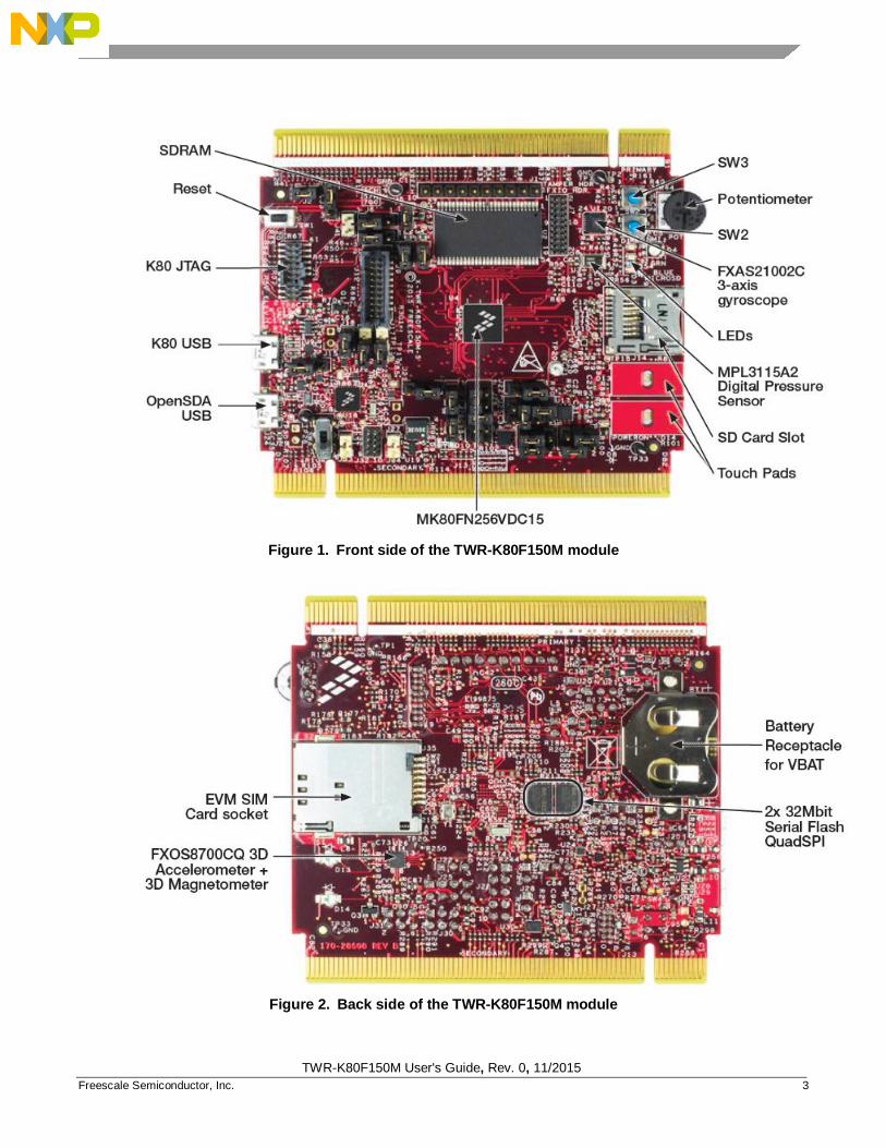
Figure 1. Front side of the TWR-K80F150M module
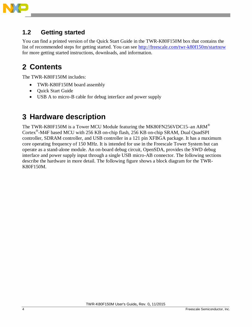
Figure 2. Back side of the TWR-K80F150M module
TWR-K80F150M User's Guide, Rev. 0, 11/2015
4 Freescale Semiconductor, Inc.
1.2 Getting started
You can find a printed version of the Quick Start Guide in the TWR-K80F150M box that contains the
list of recommended steps for getting started. You can see http://freescale.com/twr-k80f150m/startnow
for more getting started instructions, downloads, and information.
2 Contents
The TWR-K80F150M includes:
TWR-K80F150M board assembly
Quick Start Guide
USB A to micro-B cable for debug interface and power supply
3 Hardware description
The TWR-K80F150M is a Tower MCU Module featuring the MK80FN256VDC15–an ARM®
Cortex®-M4F based MCU with 256 KB on-chip flash, 256 KB on-chip SRAM, Dual QuadSPI
controller, SDRAM controller, and USB controller in a 121 pin XFBGA package. It has a maximum
core operating frequency of 150 MHz. It is intended for use in the Freescale Tower System but can
operate as a stand-alone module. An on-board debug circuit, OpenSDA, provides the SWD debug
interface and power supply input through a single USB micro-AB connector. The following sections
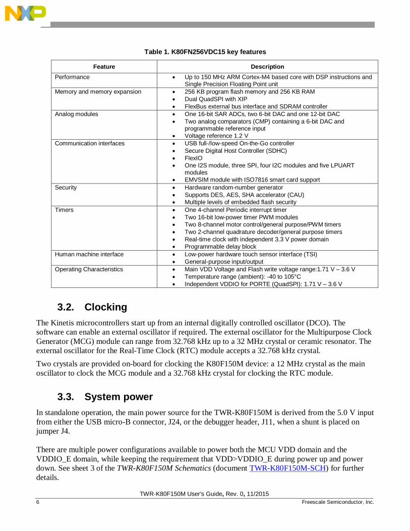
describe the hardware in more detail. The following figure shows a block diagram for the TWR-
K80F150M.
TWR-K80F150M User's Guide, Rev. 0, 11/2015
Freescale Semiconductor, Inc. 5
Figure 3. TWR-K80F150M Block Diagram
3.1. K80F150M microcontroller
The TWR-K80F150M module features the MK80FN256VDC15. The K80 microcontroller family is part
of the Kinetis portfolio of devices built around an ARM Cortex-M4F core. Refer to the K80 Family
Reference Manual (document K80P121M150SF5RM) for comprehensive information on the
K80FN256VDC15 device. The key features of K80FN256VDC15 are as follows:
TWR-K80F150M User's Guide, Rev. 0, 11/2015
6 Freescale Semiconductor, Inc.
Table 1. K80FN256VDC15 key features
Feature Description
Performance Up to 150 MHz ARM Cortex-M4 based core with DSP instructions and Single Precision Floating Point unit
Memory and memory expansion 256 KB program flash memory and 256 KB RAM
Dual QuadSPI with XIP
FlexBus external bus interface and SDRAM controller
Analog modules One 16-bit SAR ADCs, two 6-bit DAC and one 12-bit DAC
Two analog comparators (CMP) containing a 6-bit DAC and programmable reference input
Voltage reference 1.2 V
Communication interfaces USB full-/low-speed On-the-Go controller
Secure Digital Host Controller (SDHC)
FlexIO
One I2S module, three SPI, four I2C modules and five LPUART modules
EMVSIM module with ISO7816 smart card support
Security Hardware random-number generator
Supports DES, AES, SHA accelerator (CAU)
Multiple levels of embedded flash security
Timers One 4-channel Periodic interrupt timer
Two 16-bit low-power timer PWM modules
Two 8-channel motor control/general purpose/PWM timers
Two 2-channel quadrature decoder/general purpose timers
Real-time clock with independent 3.3 V power domain
Programmable delay block
Human machine interface Low-power hardware touch sensor interface (TSI)
General-purpose input/output
Operating Characteristics Main VDD Voltage and Flash write voltage range:1.71 V – 3.6 V
Temperature range (ambient): -40 to 105°C
Independent VDDIO for PORTE (QuadSPI): 1.71 V – 3.6 V
3.2. Clocking
The Kinetis microcontrollers start up from an internal digitally controlled oscillator (DCO). The
software can enable an external oscillator if required. The external oscillator for the Multipurpose Clock
Generator (MCG) module can range from 32.768 kHz up to a 32 MHz crystal or ceramic resonator. The
external oscillator for the Real-Time Clock (RTC) module accepts a 32.768 kHz crystal.
Two crystals are provided on-board for clocking the K80F150M device: a 12 MHz crystal as the main
oscillator to clock the MCG module and a 32.768 kHz crystal for clocking the RTC module.
3.3. System power
In standalone operation, the main power source for the TWR-K80F150M is derived from the 5.0 V input
from either the USB micro-B connector, J24, or the debugger header, J11, when a shunt is placed on
jumper J4.
There are multiple power configurations available to power both the MCU VDD domain and the
VDDIO_E domain, while keeping the requirement that VDD>VDDIO_E during power up and power
down. See sheet 3 of the TWR-K80F150M Schematics (document TWR-K80F150M-SCH) for further
details.
TWR-K80F150M User's Guide, Rev. 0, 11/2015
Freescale Semiconductor, Inc. 7
When installed into a Tower System, the TWR-K80F150M can be powered from either an on-board
power source or from another power source in the assembled Tower System.
The 3.3 V or 1.8 V power supplied to the MCU is routed through a jumper, J9. The jumper shunt can be
removed to allow the following:
1) Alternate MCU supply voltages to be injected.
2) Measurement of power consumed by the MCU.
3.4. Real-Time Clock supply
The Real-Time Clock (RTC) module on the K80FN256VDC15 has two modes of operation: system
power up and system power down. During system power down, the RTC can be powered from the
backup power supply (VBAT) and electrically isolated from the rest of the MCU. The TWR-K80F150M
provides a battery receptacle for a coin cell battery that can be used as the VBAT supply. The receptacle
uses standard 20 mm diameter 3 V lithium coin cell batteries.
By default the VBAT supply comes from the MCU_PWR domain. This is selected via J3.
3.5. Serial and Debug Adapter version 2 (OpenSDAv2.1)
OpenSDAv2.1 is a serial and debug adapter circuit which includes an open-source hardware design, an
open-source bootloader, and debug interface software. It bridges serial and debug communications
between a USB host and an embedded target processor as shown in figure 4. The hardware circuit is
based on a Freescale Kinetis K20 family MCU with 128 KB of embedded flash and an integrated USB
controller. OpenSDAv2 comes preloaded with the CMSIS-DAP bootloader—an open-source mass
storage device (MSD) bootloader—and the CMSIS-DAP interface firmware (also known as the mbed
interface), which provides an MSD flash programming interface, a virtual serial port interface, and a
CMSIS-DAP debug protocol interface. For more information on the OpenSDAv2 software, see
http://freescale.com/opensda
OpenSDAv2
OpenSDA MCU
K20DX128Vxx5
MSD Bootloader
OpenSDAv2
Application
UART TX/RX
GPIO
Serial Terminal
File System
SWD/JTAG
LEDPWM
USB Host
IDE GPIO/ADC
SPI, GPIO
USB
Target
Processor
nRESET
UART RX/TX
Figure 4. OpenSDAv2 high-level block diagram
TWR-K80F150M User's Guide, Rev. 0, 11/2015
8 Freescale Semiconductor, Inc.
OpenSDAv2 is managed by a Kinetis K20 MCU built on the ARM Cortex-M4 core. The OpenSDAv2
circuit includes a green status LED (D5) and a pushbutton (SW1). The pushbutton asserts the Reset
signal to the K80 target MCU. It can also be used to place the OpenSDAv2 circuit into bootloader mode.
SPI and GPIO signals provide an interface to either the SWD debug port or the K20. Additionally,
signal connections are available to implement a UART serial channel. The OpenSDAv2 circuit receives
power when the USB connector J24 is plugged into a USB host.
3.6. Cortex Debug connector
The Cortex Debug connector is a 20-pin (0.05 inch) connector providing access to the SWD and JTAG
available on the K80 device. If using the Cortex Debug connector, it is recommended to isolate the
OpenSDA circuit from the debug signals by removing the jumpers J16 and J17.
The K80 pin connections to the debug connector (J11) are shown in this table.
Table 2. Cortex Debug connector pinout
Pin Function TWR-K80F150M connection
1 VTref 3.3 V MCU supply (MCU_PWR)
2 TMS/SWDIO PTA3/JTAG_TMS/SWD_DIO
3 GND GND
4 TCK/SWCLK PTA0/JTAG_TCLK/SWD_CLK
5 GND GND
6 TDO/SWO PTA2/JTAG_TDO/TRACE_SWO
7 Key —
8 TDI PTA1/JTAG_TDI
9 GNDDETECT No Connect
10 nReset RESET_b
11 Target Power 5 V supply (via J4)
12 TRACECLK PTA12/TRACE_CLKOUT
13 Target Power 5 V supply (via J4)
14 TRACEDATA[0] PTA16/TRACE_D0
15 GND GND
16 TRACEDATA[1] PTA15TRACE_D1
17 GND GND
18 TRACEDATA[2] PTA14/TRACE_D2
19 GND GND
20 TRACEDATA[3] PTA13/TRACE_D3
3.7. QuadSPI Memory
The FRDM-K82F also includes dual QuadSPI memory with execute in place (XiP) and On The Fly AES
Decryption (OTFAD) capability. The on-board QuadSPI used is Macronix MX25U3235FZNI, which
are each 32 Mb (4MB) in size. The QuadSPI interface offers up to 100 MHz performance for Single
Data Rate (SDR). The QuadSPI is also supported by the internal Kinetis BootROM.
TWR-K80F150M User's Guide, Rev. 0, 11/2015
Freescale Semiconductor, Inc. 9
3.8. External Bus Interface – FlexBus
The K80 device features a multi-function external bus interface called the FlexBus interface controller.
This is capable of interfacing with slave-only devices. The FlexBus interface is not used directly on the
TWR-K80F150M. Instead, a subset of the FlexBus is connected to the Primary Connector so that the
external bus can access devices on Tower peripheral modules. Refer to Table 6 below and sheet 10 of
the TWR-K80F150M Schematics (document TWR-K80F150M-SCH) for more details. Note that the
Flexbus is muxed with the SDRAM signals.
3.9. SDRAM
The TWR-K80F150M board contains 64 Mb SDRAM (32-bit width) which is connected to the K80
SDRAM controller. The SDRAM signals are multiplexed with Flexbus signals. See the K80 Family
Reference Manual (document K80P121M150SF5RM) “Flexbus signal multiplexing” section and
“SDRAM SDR signal multiplexing” section on how to use the Flexbus and SDRAM in multiplexed
mode.
To use the SDRAM, jumpers J6 and J8 should be removed. This is due to the UART TX/RX lines used
on the TWR-K80F150M are muxed with the SDRAM signals. This does mean serial communication
over OpenSDA is not possible while using the SDRAM.
3.10. Sensors
There are three Freescale sensors on the board, all connected via I2C0 via PTD8 (I2C0_SCL) and PTD9
(I2C0_SDA):
FXOS8700CQ: Digital accelerometer and magnetometer
MPL3115A2: Digital pressure sensor
FXAS21002C: 3-axis gyroscope.
Each sensor also has two interrupt signals with the option to connect to the K80 device on PTA17 and
PTA29. By default they are disconnected via DNP resistors.
Table 3. Sensor types and slave addresses
Sensor I2C Slave Address
FXOS8700CQ 3D accelerometer and 3D magnetometer
0x1D
MPL3115A2 Digital pressure sensor
0x60
FXAS21002C 3-axis gyroscope 0x20
3.11. Potentiometer, pushbuttons, LEDs
The TWR-K80F150M features:
• A potentiometer connected to an ADC input signal (ADC0_DM3)
• Two pushbutton switches (SW2 and SW3 connected to PTA4 and PTA21)

TWR-K80F150M User's Guide, Rev. 0, 11/2015
10 Freescale Semiconductor, Inc.
• User controllable LEDs connected to GPIO signals
— Red LED D1 connected to PTD11
— Green LED D2 connected to PTD12
— Blue LED D3 connected to PTD13
— Green Touch LED D13 connected to PTD14
— Blue Touch LED D14 connected to PTD15
— RGB LED D5 connected via DNP resistor to PTD11, PTD12, and PTD13
3.12. Touch interface
The touch-sensing input (TSI) module of the Kinetis microcontrollers provides capacitive touch-sensing
detection with high sensitivity and enhanced robustness. Each TSI pin implements the capacitive
measurement of an electrode. There are two individual electrodes on-board the TWR-K80F150M that
simulate pushbuttons. TSI0_CH9 (PTB16) and TSI0_CH10 (PTB17) are connected to the capacitive
pads.
Figure 5. Touch pad circuitry
There is also a Touch TWRPI (Tower Plugin) header for a touch sensitive keypad to be attached on J12.
For details on the connection see Table 5.
3.13. USB interface
The K80FN256VDC15 features a full-, low-speed USB controller with on-chip USB transceiver. The
TWR-K80F150M board enables the USB to be host or device mode.
TWR-K80F150M User's Guide, Rev. 0, 11/2015
Freescale Semiconductor, Inc. 11
Jumper J20 is used to select whether the USB signals are connected to the on-board micro-B connector
J19 (default), or sent down the elevator to be used in connection with a TWR-SER1 board or other
peripheral board in a complete tower kit.
A MIC2005 device is used for over-current detection. PTC19 (connected via J28) is used to enable a 5 V
VBUS signal, and PTC18 (connected via J18) is used as an over-current signal.
3.14. Secure digital card slot
A Micro SD card slot is available on the TWR-K80F150M connected to the SD host controller (SDHC)
signals of the MCU. This slot will accept standard format SD memory cards. See Table 5 for connection
details.
The SDHC signals are muxed with the QuadSPI signals, and therefore the microSD card slot is not
connected to the K80 by default. To use the microSD card, populate the R198, R200, R208, R58, R196,
R218, and R244 resistors on the board with 0 ohm resistors. Then remove the R231 and R227 resistors
that power the QuadSPI. Finally because the microSD card slot needs to run at 3.3 V, on J31 the jumpers
should be set to 1-3 and 2-4 to make both VDD and VDDIO_E at 3.3 V.
4 Jumper table
There are several jumpers provided for isolation, configuration, and feature selection. See the following
table for details.
Table 4. TWR-K80F150M jumper table (continued)
Jumper Option Setting Description Default
setting
J2 MCU reset connection on JTAG connector
ON Connect MCU reset on pin10 of JTAG connector J11
ON OFF Disconnect MCU reset on pin10 of JTAG connector J11
J3 VBAT Power Selection
1-2 Connect VBAT to on board MCU supply from MCU_PWR
1-2 2-3 Connect VBAT to the higher voltage between on board MCU_PWR supply or coin cell supply
J4 JTAG Power Connection
ON Connect on-board 5V supply to JTAG port (supports powering board from external JTAG probe) OFF
OFF Disconnect on-board 5V supply from JTAG port
J5 QuadSPI Power Enable
ON Connect VDDIO_E domain to power QuadSPI flash. Should only be connected when VDDIO_E is at 1.8V ON
OFF Disconnect VDDIO_E domain from QuadSPI flash.
J6 UART RX Connection
1-2 Connect UART1_RX to elevator 2-3
2-3 Connect UART1_RX to OpenSDA UART RX
J8 UART TX Connection
1-2 Connect UART1_TX to elevator 2-3
2-3 Connect UART1_TX to OpenSDA UART TX
J9 MCU power connection
ON Connect V_BRD and MCU_PWR to MCU_VDD ON
OFF Disconnect V_BRD and MCU_PWR from MCU_VDD
J10 VDD and VDDA connection
ON Connect VDD and VDDA ON
OFF Disconnect VDD and VDDA
J15 USB ID connection ON Connect PTD7 to USB ID pin on micro-USB connector J19
OFF OFF Disconnect PTD7 from USB ID pin on micro-USB connector J19
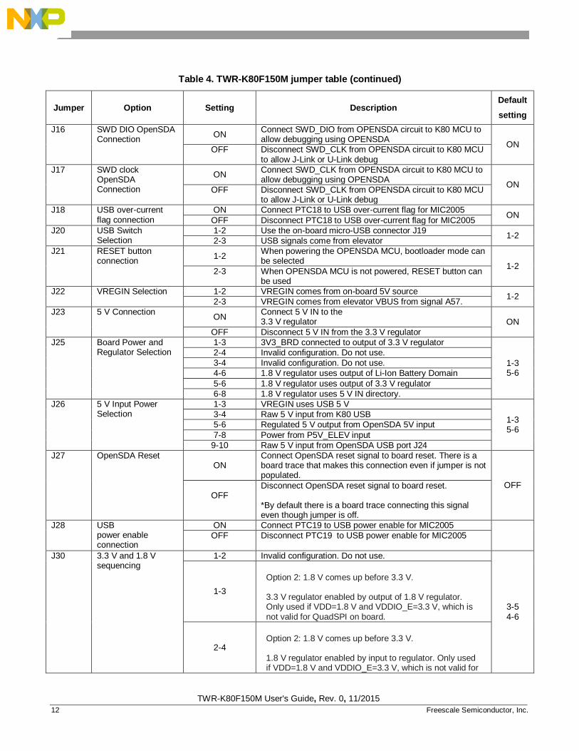
TWR-K80F150M User's Guide, Rev. 0, 11/2015
12 Freescale Semiconductor, Inc.
Table 4. TWR-K80F150M jumper table (continued)
Jumper Option Setting Description Default
setting
J16 SWD DIO OpenSDA Connection
ON Connect SWD_DIO from OPENSDA circuit to K80 MCU to allow debugging using OPENSDA
ON OFF Disconnect SWD_CLK from OPENSDA circuit to K80 MCU
to allow J-Link or U-Link debug
J17 SWD clock OpenSDA Connection
ON Connect SWD_CLK from OPENSDA circuit to K80 MCU to allow debugging using OPENSDA
ON OFF Disconnect SWD_CLK from OPENSDA circuit to K80 MCU
to allow J-Link or U-Link debug
J18 USB over-current flag connection
ON Connect PTC18 to USB over-current flag for MIC2005 ON
OFF Disconnect PTC18 to USB over-current flag for MIC2005
J20 USB Switch Selection
1-2 Use the on-board micro-USB connector J19 1-2
2-3 USB signals come from elevator
J21 RESET button connection
1-2 When powering the OPENSDA MCU, bootloader mode can be selected
1-2 2-3 When OPENSDA MCU is not powered, RESET button can
be used
J22 VREGIN Selection 1-2 VREGIN comes from on-board 5V source 1-2
2-3 VREGIN comes from elevator VBUS from signal A57.
J23 5 V Connection ON
Connect 5 V IN to the 3.3 V regulator ON
OFF Disconnect 5 V IN from the 3.3 V regulator
J25 Board Power and Regulator Selection
1-3 3V3_BRD connected to output of 3.3 V regulator
1-3 5-6
2-4 Invalid configuration. Do not use.
3-4 Invalid configuration. Do not use.
4-6 1.8 V regulator uses output of Li-Ion Battery Domain
5-6 1.8 V regulator uses output of 3.3 V regulator
6-8 1.8 V regulator uses 5 V IN directory.
J26 5 V Input Power Selection
1-3 VREGIN uses USB 5 V
1-3 5-6
3-4 Raw 5 V input from K80 USB
5-6 Regulated 5 V output from OpenSDA 5V input
7-8 Power from P5V_ELEV input
9-10 Raw 5 V input from OpenSDA USB port J24
J27 OpenSDA Reset ON
Connect OpenSDA reset signal to board reset. There is a board trace that makes this connection even if jumper is not populated.
OFF
OFF Disconnect OpenSDA reset signal to board reset.
*By default there is a board trace connecting this signaleven though jumper is off.
J28 USB power enable connection
ON Connect PTC19 to USB power enable for MIC2005
OFF Disconnect PTC19 to USB power enable for MIC2005
J30 3.3 V and 1.8 V sequencing
1-2 Invalid configuration. Do not use.
3-5 4-6
1-3
Option 2: 1.8 V comes up before 3.3 V.
3.3 V regulator enabled by output of 1.8 V regulator. Only used if VDD=1.8 V and VDDIO_E=3.3 V, which is not valid for QuadSPI on board.
2-4 Option 2: 1.8 V comes up before 3.3 V.
1.8 V regulator enabled by input to regulator. Only used if VDD=1.8 V and VDDIO_E=3.3 V, which is not valid for
TWR-K80F150M User's Guide, Rev. 0, 11/2015
Freescale Semiconductor, Inc. 13
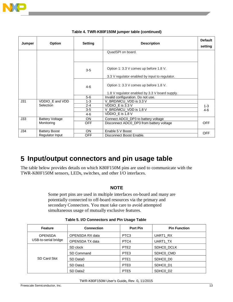
Table 4. TWR-K80F150M jumper table (continued)
Jumper Option Setting Description Default
setting
QuadSPI on board.
3-5 Option 1: 3.3 V comes up before 1.8 V.
3.3 V regulator enabled by input to regulator.
4-6 Option 1: 3.3 V comes up before 1.8 V.
1.8 V regulator enabled by 3.3 V board supply.
5-6 Invalid configuration. Do not use.
J31 VDDIO_E and VDD Selection
1-3 V_BRD/MCU_VDD is 3.3 V
1-3 4-6
2-4 VDDIO_E is 3.3 V
3-5 V_BRD/MCU_VDD is 1.8 V
4-6 VDDIO_E is 1.8 V
J33 Battery Voltage Monitoring
ON Connect ADC0_DP3 to battery voltage OFF OFF Disconnect ADC0_DP3 from battery voltage
J34 Battery Boost Regulator Input
ON Enable 5 V Boost OFF
OFF Disconnect Boost Enable.
5 Input/output connectors and pin usage table
The table below provides details on which K80F150M pins are used to communicate with the
TWR-K80F150M sensors, LEDs, switches, and other I/O interfaces.
NOTE
Some port pins are used in multiple interfaces on-board and many are
potentially connected to off-board resources via the primary and
secondary Connectors. You must take care to avoid attempted
simultaneous usage of mutually exclusive features.
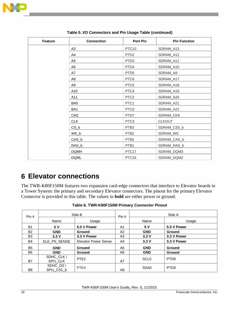
Table 5. I/O Connectors and Pin Usage Table (continued)
Feature Connection Port Pin Pin Function
OPENSDA
USB-to-serial bridge
OPENSDA RX data PTC3 UART1_RX
OPENSDA TX data PTC4 UART1_TX
SD Card Slot
SD clock PTE2 SDHC0_DCLK
SD Command PTE3 SDHC0_CMD
SD Data0 PTE1 SDHC0_D0
SD Data1 PTE0 SDHC0_D1
SD Data2 PTE5 SDHC0_D2
TWR-K80F150M User's Guide, Rev. 0, 11/2015
14 Freescale Semiconductor, Inc.
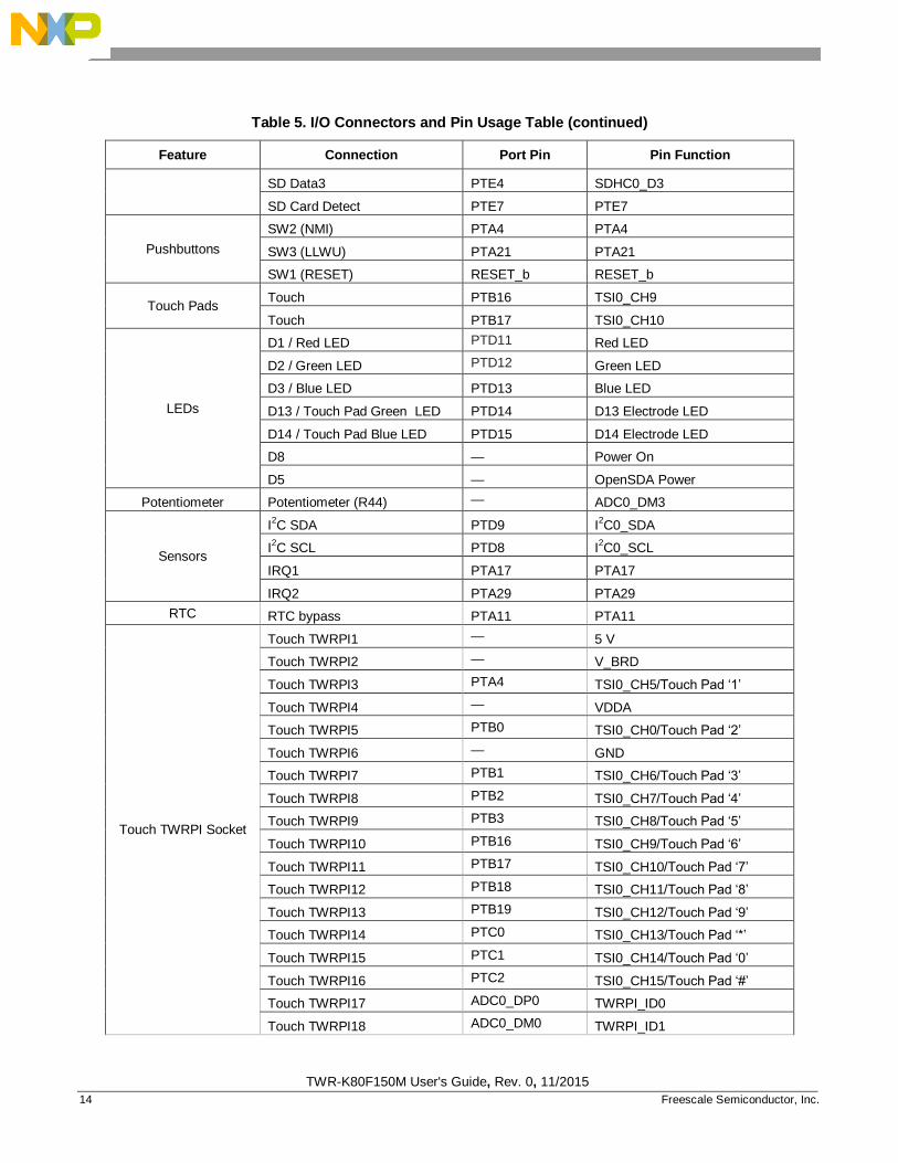
Table 5. I/O Connectors and Pin Usage Table (continued)
Feature Connection Port Pin Pin Function
SD Data3 PTE4 SDHC0_D3
SD Card Detect PTE7 PTE7
Pushbuttons
SW2 (NMI) PTA4 PTA4
SW3 (LLWU) PTA21 PTA21
SW1 (RESET) RESET_b RESET_b
Touch Pads Touch PTB16 TSI0_CH9
Touch PTB17 TSI0_CH10
LEDs
D1 / Red LED PTD11 Red LED
D2 / Green LED PTD12 Green LED
D3 / Blue LED PTD13 Blue LED
D13 / Touch Pad Green LED PTD14 D13 Electrode LED
D14 / Touch Pad Blue LED PTD15 D14 Electrode LED
D8 — Power On
D5 — OpenSDA Power
Potentiometer Potentiometer (R44) — ADC0_DM3
Sensors
I2C SDA PTD9 I
2C0_SDA
I2C SCL PTD8 I
2C0_SCL
IRQ1 PTA17 PTA17
IRQ2 PTA29 PTA29
RTC RTC bypass PTA11 PTA11
Touch TWRPI Socket
Touch TWRPI1 — 5 V
Touch TWRPI2 — V_BRD
Touch TWRPI3 PTA4 TSI0_CH5/Touch Pad ‘1’
Touch TWRPI4 — VDDA
Touch TWRPI5 PTB0 TSI0_CH0/Touch Pad ‘2’
Touch TWRPI6 — GND
Touch TWRPI7 PTB1 TSI0_CH6/Touch Pad ‘3’
Touch TWRPI8 PTB2 TSI0_CH7/Touch Pad ‘4’
Touch TWRPI9 PTB3 TSI0_CH8/Touch Pad ‘5’
Touch TWRPI10 PTB16 TSI0_CH9/Touch Pad ‘6’
Touch TWRPI11 PTB17 TSI0_CH10/Touch Pad ‘7’
Touch TWRPI12 PTB18 TSI0_CH11/Touch Pad ‘8’
Touch TWRPI13 PTB19 TSI0_CH12/Touch Pad ‘9’
Touch TWRPI14 PTC0 TSI0_CH13/Touch Pad ‘*’
Touch TWRPI15 PTC1 TSI0_CH14/Touch Pad ‘0’
Touch TWRPI16 PTC2 TSI0_CH15/Touch Pad ‘#’
Touch TWRPI17 ADC0_DP0 TWRPI_ID0
Touch TWRPI18 ADC0_DM0 TWRPI_ID1
TWR-K80F150M User's Guide, Rev. 0, 11/2015
Freescale Semiconductor, Inc. 15
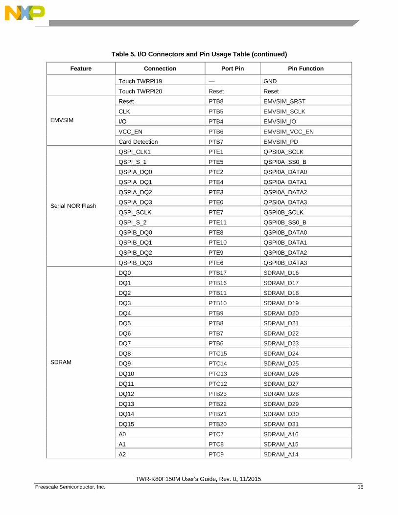
Table 5. I/O Connectors and Pin Usage Table (continued)
Feature Connection Port Pin Pin Function
Touch TWRPI19 — GND
Touch TWRPI20 Reset Reset
EMVSIM
Reset PTB8 EMVSIM_SRST
CLK PTB5 EMVSIM_SCLK
I/O PTB4 EMVSIM_IO
VCC_EN PTB6 EMVSIM_VCC_EN
Card Detection PTB7 EMVSIM_PD
Serial NOR Flash
QSPI_CLK1 PTE1 QPSI0A_SCLK
QSPI_S_1 PTE5 QSPI0A_SS0_B
QSPIA_DQ0 PTE2 QSPI0A_DATA0
QSPIA_DQ1 PTE4 QSPI0A_DATA1
QSPIA_DQ2 PTE3 QSPI0A_DATA2
QSPIA_DQ3 PTE0 QPSI0A_DATA3
QSPI_SCLK PTE7 QSPI0B_SCLK
QSPI_S_2 PTE11 QSPI0B_SS0_B
QSPIB_DQ0 PTE8 QSPI0B_DATA0
QSPIB_DQ1 PTE10 QSPI0B_DATA1
QSPIB_DQ2 PTE9 QSPI0B_DATA2
QSPIB_DQ3 PTE6 QSPI0B_DATA3
SDRAM
DQ0 PTB17 SDRAM_D16
DQ1 PTB16 SDRAM_D17
DQ2 PTB11 SDRAM_D18
DQ3 PTB10 SDRAM_D19
DQ4 PTB9 SDRAM_D20
DQ5 PTB8 SDRAM_D21
DQ6 PTB7 SDRAM_D22
DQ7 PTB6 SDRAM_D23
DQ8 PTC15 SDRAM_D24
DQ9 PTC14 SDRAM_D25
DQ10 PTC13 SDRAM_D26
DQ11 PTC12 SDRAM_D27
DQ12 PTB23 SDRAM_D28
DQ13 PTB22 SDRAM_D29
DQ14 PTB21 SDRAM_D30
DQ15 PTB20 SDRAM_D31
A0 PTC7 SDRAM_A16
A1 PTC8 SDRAM_A15
A2 PTC9 SDRAM_A14
TWR-K80F150M User's Guide, Rev. 0, 11/2015
16 Freescale Semiconductor, Inc.
Table 5. I/O Connectors and Pin Usage Table (continued)
Feature Connection Port Pin Pin Function
A3 PTC10 SDRAM_A13
A4 PTD2 SDRAM_A12
A5 PTD3 SDRAM_A11
A6 PTD4 SDRAM_A10
A7 PTD5 SDRAM_A9
A8 PTC6 SDRAM_A17
A9 PTC5 SDRAM_A18
A10 PTC4 SDRAM_A19
A11 PTC2 SDRAM_A20
BA0 PTC1 SDRAM_A21
BA1 PTC0 SDRAM_A22
CKE PTD7 SDRAM_CKE
CLK PTC3 CLKOUT
CS_b PTB3 SDRAM_CS0_b
WE_b PTB2 SDRAM_WE
CAS_b PTB0 SDRAM_CAS_b
RAS_b PTB1 SDRAM_RAS_b
DQMH PTC17 SDRAM_DQM3
DQML PTC16 SDRAM_DQM2
6 Elevator connections
The TWR-K80F150M features two expansion card-edge connectors that interface to Elevator boards in
a Tower System: the primary and secondary Elevator connectors. The pinout for the primary Elevator
Connector is provided in this table. The values in bold are either power or ground.
Table 6. TWR-K80F150M Primary Connector Pinout
Pin # Side B
Pin # Side A
Name Usage Name Usage
B1 5 V 5.0 V Power A1 5 V 5.0 V Power
B2 GND Ground A2 GND Ground
B3 3.3 V 3.3 V Power A3 3.3 V 3.3 V Power
B4 ELE_PS_SENSE Elevator Power Sense A4 3.3 V 3.3 V Power
B5 GND Ground A5 GND Ground
B6 GND Ground A6 GND Ground
B7
SDHC_CLK /
SPI1_CLK PTE2
A7 SCL0 PTD8
B8
SDHC_D3 /
SPI1_CS1_b PTE4
A8 SDA0 PTD9
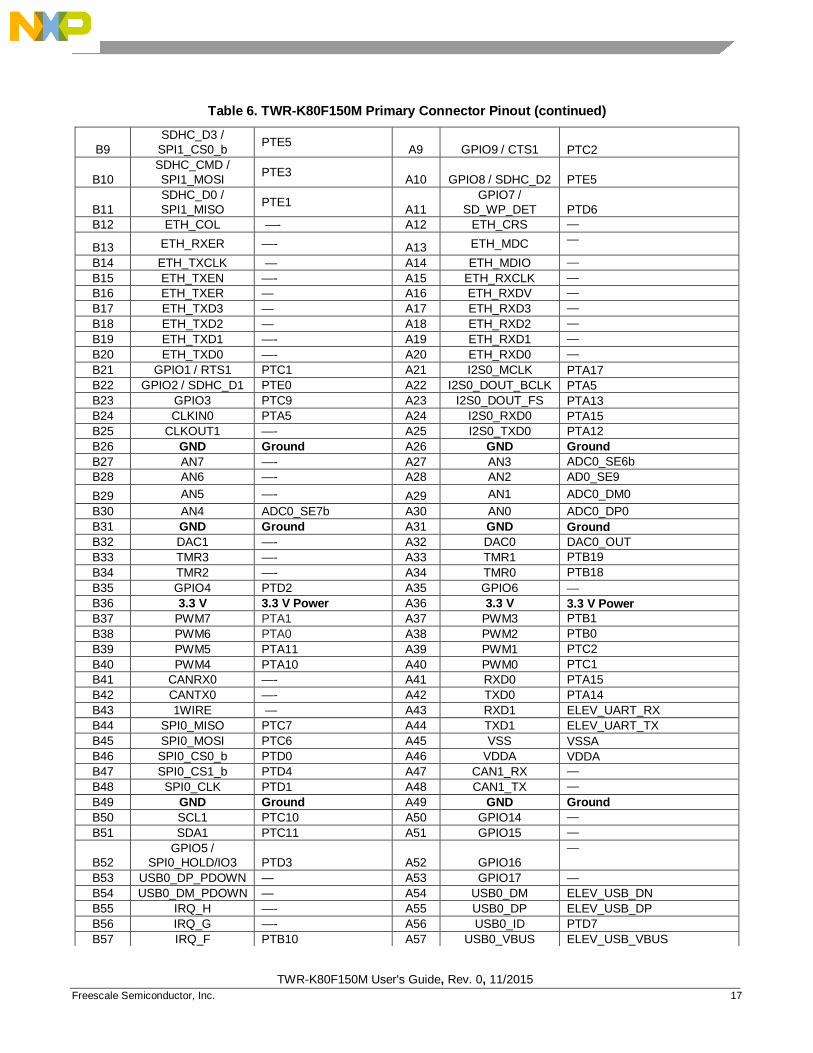
TWR-K80F150M User's Guide, Rev. 0, 11/2015
Freescale Semiconductor, Inc. 17
Table 6. TWR-K80F150M Primary Connector Pinout (continued)
B9
SDHC_D3 /
SPI1_CS0_b PTE5
A9 GPIO9 / CTS1 PTC2
B10
SDHC_CMD /
SPI1_MOSI PTE3
A10 GPIO8 / SDHC_D2 PTE5
B11
SDHC_D0 /
SPI1_MISO PTE1
A11
GPIO7 /
SD_WP_DET PTD6
B12 ETH_COL —- A12 ETH_CRS —
B13 ETH_RXER —- A13 ETH_MDC —
B14 ETH_TXCLK — A14 ETH_MDIO —
B15 ETH_TXEN —- A15 ETH_RXCLK —
B16 ETH_TXER — A16 ETH_RXDV —
B17 ETH_TXD3 — A17 ETH_RXD3 —
B18 ETH_TXD2 — A18 ETH_RXD2 —
B19 ETH_TXD1 —- A19 ETH_RXD1 —
B20 ETH_TXD0 —- A20 ETH_RXD0 —
B21 GPIO1 / RTS1 PTC1 A21 I2S0_MCLK PTA17
B22 GPIO2 / SDHC_D1 PTE0 A22 I2S0_DOUT_BCLK PTA5
B23 GPIO3 PTC9 A23 I2S0_DOUT_FS PTA13
B24 CLKIN0 PTA5 A24 I2S0_RXD0 PTA15
B25 CLKOUT1 —- A25 I2S0_TXD0 PTA12
B26 GND Ground A26 GND Ground
B27 AN7 —- A27 AN3 ADC0_SE6b
B28 AN6 —- A28 AN2 AD0_SE9
B29 AN5 —- A29 AN1 ADC0_DM0
B30 AN4 ADC0_SE7b A30 AN0 ADC0_DP0
B31 GND Ground A31 GND Ground
B32 DAC1 —- A32 DAC0 DAC0_OUT
B33 TMR3 —- A33 TMR1 PTB19
B34 TMR2 —- A34 TMR0 PTB18
B35 GPIO4 PTD2 A35 GPIO6 —
B36 3.3 V 3.3 V Power A36 3.3 V 3.3 V Power
B37 PWM7 PTA1 A37 PWM3 PTB1
B38 PWM6 PTA0 A38 PWM2 PTB0
B39 PWM5 PTA11 A39 PWM1 PTC2
B40 PWM4 PTA10 A40 PWM0 PTC1
B41 CANRX0 —- A41 RXD0 PTA15
B42 CANTX0 —- A42 TXD0 PTA14
B43 1WIRE — A43 RXD1 ELEV_UART_RX
B44 SPI0_MISO PTC7 A44 TXD1 ELEV_UART_TX
B45 SPI0_MOSI PTC6 A45 VSS VSSA
B46 SPI0_CS0_b PTD0 A46 VDDA VDDA
B47 SPI0_CS1_b PTD4 A47 CAN1_RX —
B48 SPI0_CLK PTD1 A48 CAN1_TX —
B49 GND Ground A49 GND Ground
B50 SCL1 PTC10 A50 GPIO14 —
B51 SDA1 PTC11 A51 GPIO15 —
B52
GPIO5 /
SPI0_HOLD/IO3 PTD3 A52 GPIO16
—
B53 USB0_DP_PDOWN — A53 GPIO17 —
B54 USB0_DM_PDOWN — A54 USB0_DM ELEV_USB_DN
B55 IRQ_H —- A55 USB0_DP ELEV_USB_DP
B56 IRQ_G —- A56 USB0_ID PTD7
B57 IRQ_F PTB10 A57 USB0_VBUS ELEV_USB_VBUS
TWR-K80F150M User's Guide, Rev. 0, 11/2015
18 Freescale Semiconductor, Inc.
7 References
The list below provides references for more information on the Kinetis family, Tower System and the
MCU modules. These can be found in the documentation section of freescale.com/TWR-K80F150M or
freescale.com/kinetis.
• TWR-K80F150M Quick Start Guide (document TWR-K80F150M-QSG)
• TWR-K80F150M Schematics (document TWR-K80F150M-SCH)
• K80 Family Data Sheet (document K80P121M150SF5)
• K80 Family Reference Manual (document K80P121M150SF5RM)
• Kinetis Quick Reference User Guide (document KQRUG)
• Kinetis Software Development Kit (http://freescale.com/ksdk)
• Kinetis Bootloader (http://freescale.com/kboot)
8 Revision history Table 7. Revision history
Revision Number Date Substantive changes
0 11/2015 Initial release
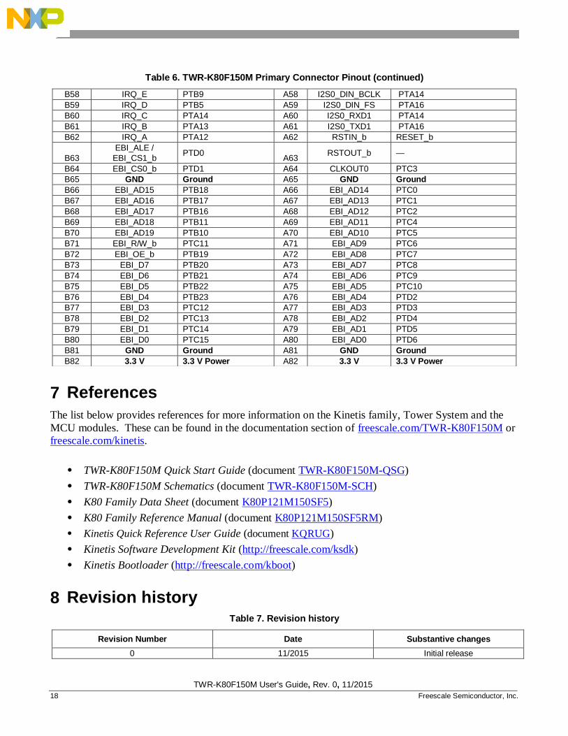
Table 6. TWR-K80F150M Primary Connector Pinout (continued)
B58 IRQ_E PTB9 A58 I2S0_DIN_BCLK PTA14
B59 IRQ_D PTB5 A59 I2S0_DIN_FS PTA16
B60 IRQ_C PTA14 A60 I2S0_RXD1 PTA14
B61 IRQ_B PTA13 A61 I2S0_TXD1 PTA16
B62 IRQ_A PTA12 A62 RSTIN_b RESET_b
B63
EBI_ALE /
EBI_CS1_b PTD0
A63 RSTOUT_b —
B64 EBI_CS0_b PTD1 A64 CLKOUT0 PTC3
B65 GND Ground A65 GND Ground
B66 EBI_AD15 PTB18 A66 EBI_AD14 PTC0
B67 EBI_AD16 PTB17 A67 EBI_AD13 PTC1
B68 EBI_AD17 PTB16 A68 EBI_AD12 PTC2
B69 EBI_AD18 PTB11 A69 EBI_AD11 PTC4
B70 EBI_AD19 PTB10 A70 EBI_AD10 PTC5
B71 EBI_R/W_b PTC11 A71 EBI_AD9 PTC6
B72 EBI_OE_b PTB19 A72 EBI_AD8 PTC7
B73 EBI_D7 PTB20 A73 EBI_AD7 PTC8
B74 EBI_D6 PTB21 A74 EBI_AD6 PTC9
B75 EBI_D5 PTB22 A75 EBI_AD5 PTC10
B76 EBI_D4 PTB23 A76 EBI_AD4 PTD2
B77 EBI_D3 PTC12 A77 EBI_AD3 PTD3
B78 EBI_D2 PTC13 A78 EBI_AD2 PTD4
B79 EBI_D1 PTC14 A79 EBI_AD1 PTD5
B80 EBI_D0 PTC15 A80 EBI_AD0 PTD6
B81 GND Ground A81 GND Ground
B82 3.3 V 3.3 V Power A82 3.3 V 3.3 V Power
Document Number: TWRK80F150MUG Rev. 0
11/2015
How to Reach Us:
Home Page:
freescale.com
Web Support:
freescale.com/support
Information in this document is provided solely to enable system and software
implementers to use Freescale products. There are no express or implied copyright
licenses granted hereunder to design or fabricate any integrated circuits based on the
information in this document.
Freescale reserves the right to make changes without further notice to any products
herein. Freescale makes no warranty, representation, or guarantee regarding the
suitability of its products for any particular purpose, nor does Freescale assume any
liability arising out of the application or use of any product or circuit, and specifically
disclaims any and all liability, including without limitation consequential or incidental
damages. “Typical” parameters that may be provided in Freescale data sheets and/or
specifications can and do vary in different applications, and actual performance may
vary over time. All operating parameters, including “typicals,” must be validated for each
customer application by customer's technical experts. Freescale does not convey any
license under its patent rights nor the rights of others. Freescale sells products pursuant
to standard terms and conditions of sale, which can be found at the following address:
freescale.com/SalesTermsandConditions.
Freescale, the Freescale logo and Kinetis are trademarks of Freescale Semiconductor,
Inc., Reg. U.S. Pat. & Tm. Off. All other product or service names are the property of
their respective owners. ARM, ARM Powered, the ARM logo, mbed, and Cortex are
registered trademarks of ARM Limited (or its subsidiaries) in the EU and/or elsewhere.
© 2015 Freescale Semiconductor, Inc. . All rights reserved.