Embed Size (px)
Citation preview

Freescale Semiconductor Inc.
TWR-SER2 User’s Manual
Rev. 1.2

TWR-SER2 User’s Manual Page 2 of 17
Contents 1 Overview ...................................................................................................................................................... 3
2 Reference Documents .............................................................................................................................. 5
3 Hardware Features ................................................................................................................................... 5 3.1 Power Supply ....................................................................................................................................................................... 6 3.2 Dual Ethernet PHYs ........................................................................................................................................................... 6 3.3 Hi-Speed Dual Role USB ................................................................................................................................................... 6 3.4 Low/Full-Speed Host USB............................................................................................................................................... 7 3.5 Serial Communications Interface ................................................................................................................................ 7
3.5.1 RS-232/485 Interface ....................................................................................................................................................................... 7 3.5.2 Serial-to-USB ........................................................................................................................................................................................ 8 3.5.3 Additonal RS232 Interfaces ........................................................................................................................................................... 8
3.6 CAN Bus .................................................................................................................................................................................. 9 3.7 Elevator Connections ..................................................................................................................................................... 10
4 Configuration Settings .......................................................................................................................... 15 4.1 Switch Settings ................................................................................................................................................................. 15 4.2 Jumper Settings ................................................................................................................................................................ 16
5 Mechanical Form Factor ...................................................................................................................... 17

TWR-SER2 User’s Manual Page 3 of 17
1 Overview
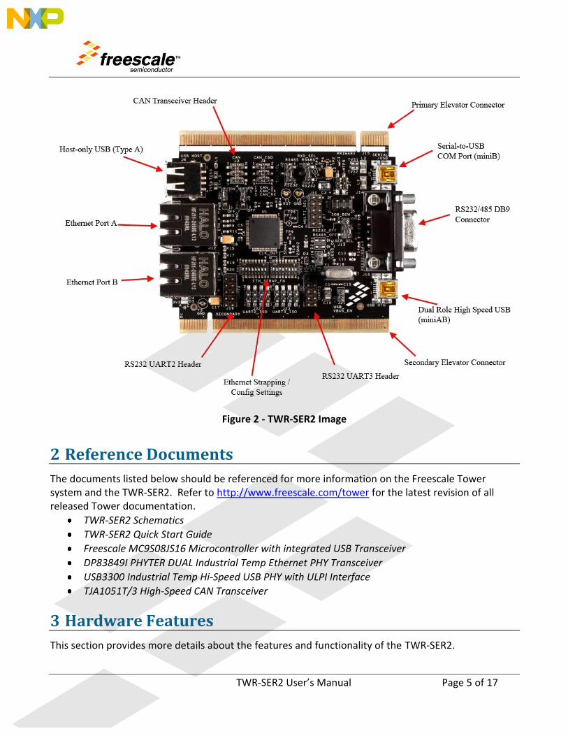
The Serial2 Tower Board (TWR-SER2) is a peripheral Tower System Module designed to be used with a compatible MCU/MPU Tower Card. The TWR-SER2 provides additional interfaces that are common to feature rich MPU’s. The TWR-SER2 features the following:
Industrial-grade Dual Ethernet PHY Transceiver w/ dual RJ-45 Ethernet Jacks, with integrated magnetics and LED’s
Industrial-grade High Speed Dual Role USB PHY (utilizes MPU’s ULPI interface)
Full Speed / Low Speed Host only USB (utilizes USB Host controller interface)
Four Serial Ports o Serial-to-USB (MC9S08JS16) w/ USB mini-B connector o RS-232 / RS-485 Transceivers on shared DB9 connector o 2x RS-232 Transceivers with option for full flow control on 2x5 Headers
A block diagram for the TWR-SER2 is shown in the figure below.

TWR-SER2 User’s Manual Page 4 of 17
DP/DN
ULPI
CAN RX/TX
RMII1MII / RMII0
RX/TX
DP/DN
UART0
SMSC
USB3300
US
B m
ini-
B
(OT
G)
US
B A
(HO
ST
)
Se
co
nd
ary
Ele
va
tor
Co
nn
ectio
n
RJ-4
5 J
ack
RJ-4
5 J
ack
National Semi
DP83849I
Strap Option Jumpers
MII/RMII Signal Select
Pri
ma
ry E
leva
tor
Co
nn
ectio
n
NXP
TJA1050
2x5 Header
CAN Bus Pin Out
CAN Isolation
Jumpers
DB9
Freescale
MC9S08JS16U
SB
min
i-B
(Se
ria
l C
OM
)
Intersil
ICL3225
(RS-232)
Intersil
ISL3176
(RS-485)
Selection / Isolation Jumpers
RS-232 / RS-485
Intersil
ICL3225
(RS-232)
Intersil
ICL3225
(RS-232)
2x5 Header
2x5 Header
Isolation
Jumpers
Isolation
Jumpers
Isolation
Jumpers
Serial-to-USB Dual Ethernet
CAN
RS-232 (w/ optional flow control) – 2x5 Header Interface
RS-232 or RS-485
DB9 Interface
USB OTG /
USB Host
CANH/
CANL
RX/
TX
UART2
UART3
RXD/TXD
CTS/RTS
RS-232
RXs/TXs
UART1
RXD/TXD
CTS/RTS
RXD/TXD
RS-232
RX/TX
RS-495
RX/TX
RS-232
RXs/TXs
USB DP/DM
TPTD/TPRD
LEDs
Figure 1 - TWR-SER2 Block Diagram
TWR-SER2 User’s Manual Page 5 of 17
Figure 2 - TWR-SER2 Image
2 Reference Documents
The documents listed below should be referenced for more information on the Freescale Tower system and the TWR-SER2. Refer to http://www.freescale.com/tower for the latest revision of all released Tower documentation.
TWR-SER2 Schematics
TWR-SER2 Quick Start Guide
Freescale MC9S08JS16 Microcontroller with integrated USB Transceiver
DP83849I PHYTER DUAL Industrial Temp Ethernet PHY Transceiver
USB3300 Industrial Temp Hi-Speed USB PHY with ULPI Interface
TJA1051T/3 High-Speed CAN Transceiver
3 Hardware Features
This section provides more details about the features and functionality of the TWR-SER2.

TWR-SER2 User’s Manual Page 6 of 17
3.1 Power Supply It is intended that the TWR-SER2 be powered from a source in an assembled Tower System via the 5.0V and 3.3V supplies on the TWR-ELEV. This includes the functional Tower Elevator USB power connector, a capable MCU/MPU controller module, or other Tower System module capable of providing power to the entire Tower System. The TWR-SER2 is can also provide power to the Tower System when configured and used as a USB device through the Hi-Speed USB connection (Jumper J24).
3.2 Dual Ethernet PHYs The TWR-SER2 module utilizes an industrial applicable National Semiconductor Dual Ethernet PHY Transceiver (DP83849I). The DP83849I features two fully independent 10/100 ports for multi-port applications. The TWR-SER2 is capable of supporting a single MII interface, a single RMII interface, or dual RMII interfaces. The Ethernet PHY is configurable via two sets of micro dip switches (SW1 and SW2). Refer to these settings for typical Ethernet setting. For specific setting details refer to the TWR-SER2 Jumper Options section.
10/100 Dual RMII o J8 and J9 should be un-shunted o Configure SW1 (1-8) as 11000000 o Configure SW2 (1-8) as 10100000
10/100 Signal Port RMII o J9 should be un-shunted o Configure SW1 (1-8) as 11000000 o Configure SW2 (1-8) as 10100000
10/100 Signal Port MII o J9 should be un-shunted o Configure SW1 (1-8) as 00110000 o Configure SW2 (1-8) as 00010000
3.3 Hi-Speed Dual Role USB The TWR-SER2 features Hi-Speed Dual Role USB. This feature is implemented using the SMSC USB3300 USB Transceiver with ULPI interface. The ULPI interface is connected to the TWR-SER2 PCI edge connector connect to a Tower MCU module.
Refer to these settings to configure the High Speed USB ULPI Transceiver.
Host Mode – TWR-SER2 will be connected to a device, such as a USB Memory Stick using the
appropriate mini USB adaptor.
o J24 should be un-shunted
TWR-SER2 User’s Manual Page 7 of 17
Device Mode – TWR-SER2 will be connected to a host, such as a host PC.
o J24 should be shunted, if it is desired that the entire Tower system be powered via this
connection.
3.4 Low/Full-Speed Host USB The TWR-SER2 features a Host Type-A USB receptacle. The USB differential signals are connected directly to the Tower Elevator USB Signals and will be connected to a compatible Tower System MCU/MPU module’s USB Host controller. In addition to the differential data pair, the MCU should provide the VBUS_EN signal and respond to the VBUS_OC signals. J16 and J21 should be shunted to connect VBUS enable/over-current control to the MCU signals.
3.5 Serial Communications Interface The TWR-SER2 is capable of providing up to four additional SCI’s. The number of accessible SCI’s on the TWR-SER2 will depend on the capabilities and Tower Elevator signals connections of the MCU/MPU Module.
3.5.1 RS-232/485 Interface
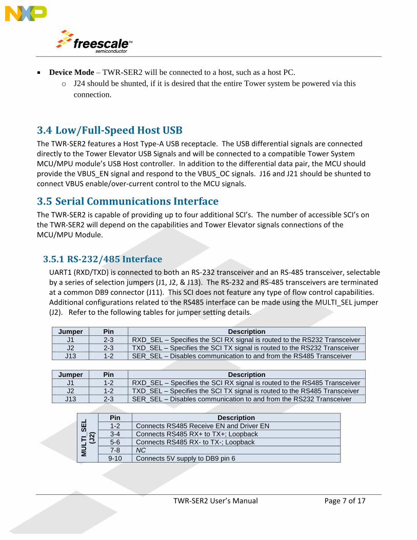
UART1 (RXD/TXD) is connected to both an RS-232 transceiver and an RS-485 transceiver, selectable by a series of selection jumpers (J1, J2, & J13). The RS-232 and RS-485 transceivers are terminated at a common DB9 connector (J11). This SCI does not feature any type of flow control capabilities. Additional configurations related to the RS485 interface can be made using the MULTI_SEL jumper (J2). Refer to the following tables for jumper setting details.
Jumper Pin Description
J1 2-3 RXD_SEL – Specifies the SCI RX signal is routed to the RS232 Transceiver
J2 2-3 TXD_SEL – Specifies the SCI TX signal is routed to the RS232 Transceiver
J13 1-2 SER_SEL – Disables communication to and from the RS485 Transceiver
Jumper Pin Description
J1 1-2 RXD_SEL – Specifies the SCI RX signal is routed to the RS485 Transceiver
J2 1-2 TXD_SEL – Specifies the SCI TX signal is routed to the RS485 Transceiver
J13 2-3 SER_SEL – Disables communication to and from the RS232 Transceiver
MU
LT
I_S
EL
(J2)
Pin Description
1-2 Connects RS485 Receive EN and Driver EN
3-4 Connects RS485 RX+ to TX+; Loopback
5-6 Connects RS485 RX- to TX-; Loopback
7-8 NC
9-10 Connects 5V supply to DB9 pin 6

TWR-SER2 User’s Manual Page 8 of 17
3.5.2 Serial-to-USB
UART0 (RXD/TXD) is connected to a Freescale MC9S08JS16. The MC9S08JS16 provides a Serial-to-USB conversion that will transmit/receive external data via its USB transceiver connected to an USB mini-B connector. When this USB receptacle is connected to a host PC it will enumerate as a USB CDC. The driver required for the CDC device is located on the included CD and is also available on the TWR-SER2 webpage found at www.freescale.com/tower.
If needed the UART0 transceiver signals can be isolated from the Tower Elevator using J7.
Pins Description
1-2 Remove to Isolate UART0_TX
3-4 Remove to Isolate UART0_RX
3.5.3 Additonal RS232 Interfaces
UART2 and UART3 (RXD/TXD/RTS/CTS) are connected to additional RS-232 transceivers. The RS-232 transceivers are terminated to 2x5 headers (refer to table for pinout). These interfaces are capable of utilizing the optional RTS/CTS signals for flow control.
J19 & J20
Pin # Signal Name
1 NC
2 NC
3 RXD
4 RTS
5 TXD
6 CTS
7 NC
8 NC
9 GND
10 NC

TWR-SER2 User’s Manual Page 9 of 17
The 2x5 header is intended to be used with a DB-9 Male to 10 PIN IDC socket adaptor cable. The cable should conform to the following pin assignments.
10 Pin IDC 0.1” 2x5 DB-9 Male Function
1 1 DCD
2 6 DSR
3 2 RX
4 7 RTS
5 3 TX
6 8 CTS
7 4 DTR
8 9 RI
9 5 GND
10 NC NC
By default the UART2 and UART3 transceiver signals are isolated from the Tower Elevator. The signals can be connected to the Tower Elevator connector using J22 and J23 respectively.
Pins Description
1-2 Remove to Isolate UARTx_TX
3-4 Remove to Isolate UARTx_RX
5-6 Remove to Isolate UARTx_RTS
7-8 Remove to Isolate UARTx_CTS
3.6 CAN Bus The TWR-SER2 features a Controller Area Network interface using an NXP TJA1051T/3 CAN transceiver. The signals from the transceiver are connected to a 6-pin (2x3) header using the following CAN Bus Pin Out.
Pin # Signal Names Signal Description
1 Not Used
2 CAN_V+ Power
3 CAN_GND Ground
4 CAN_L Dominant Low
5 CAN_H Dominant High
6 Not Used
Table 1 – 2x3 Header CAN Bus Pin Out

TWR-SER2 User’s Manual Page 10 of 17
If needed the CAN transceiver signals can be isolated from the Tower Elevator using J4.
Pins Description
1-2 Remove to Isolate CAN_S
3-4 Remove to Isolate CAN_TX
5-6 Remove to Isolate CAN_RX
3.7 Elevator Connections The TWR-SER2 features two expansion card-edge connectors that interface to Elevator boards in a Tower System: the Primary and Secondary Elevator connectors. Table 2 provides the pinout for the Primary and Secondary Elevator Connector. An “X” in the “Used” column indicated that there is a connection from the TWR-MEM to that pin on the Elevator connector. An “X” in the “Jmp” column indicates that a jumper is available that can configure or isolate the connection from the Elevator connector.
Table 2 - TWR-SER2 Primary Elevator Connector Pinout
TWR-SER2 Primary Connector
Pin Name Usage Used Jmp Pin Name Usage Used Jmp
B1 5V 5.0V Power X A1 5V 5.0V Power X
B2 GND Ground X A2 GND Ground X
B3 3.3V 3.3V Power X A3 3.3V 3.3V Power X
B4 ELE_PS_SENSE Elevator Power Sense X A4 3.3V 3.3V Power X
B5 GND Ground X A5 GND Ground X
B6 GND Ground X A6 GND Ground X
B7 SDHC_CLK / SPI1_CLK A7 I2C0_SCL
B8 SDHC_D3 / SPI1_CS1_b A8 I2C0_SDA
B9 SDHC_D3 / SPI1_CS0_b A9 GPIO9 / UART1_CTS
B10 SDHC_CMD / SPI1_MOSI A10 GPIO8 / SDHC_D2
B11 SDHC_D0 / SPI1_MISO A11 GPIO7 / SD_WP_DET
B12 ETH_COL MII_COL X A12 ETH_CRS MII_CRS X
B13 ETH_RXER MII_RXER / RMII0_RXER
X
A13 ETH_MDC
MII_MDC / RMII0_MDC
X
B14 ETH_TXCLK MII_TXCLK
X
A14 ETH_MDIO
MII_MDIO / RMII0_MDIO
X
B15 ETH_TXEN MII_TXEN / RMII0_TXEN X A15 ETH_RXCLK MII_RXCLK X
B16 ETH_TXER
A16 ETH_RXDV
MII_RXDV / RMII0_CRS_DV
X
B17 ETH_TXD3 MII_TXD3 X A17 ETH_RXD3 MII_RXD3 X
B18 ETH_TXD2 MII_TXD2 X A18 ETH_RXD2 MII_RXD2 X
B19 ETH_TXD1 MII_TXD1 / RMII0_TXD1
X
A19 ETH_RXD1
MII_RXD1 / RMII0_RXD1
X
B20 ETH_TXD0 MII_TXD0 / RMII0_TXD0
X
A20 ETH_RXD0
MII_RXD0 / RMII0_RXD0
X
B21 GPIO1 /UART1_RTS X A21 I2S0_MCLK

TWR-SER2 User’s Manual Page 11 of 17
TWR-SER2 Primary Connector
Pin Name Usage Used Jmp Pin Name Usage Used Jmp
B22 GPIO2 / SDHC_D1 X A22 I2S0_DOUT_SCK
B23 GPIO3 A23 I2S0_DOUT_WS
B24 CLKIN0 RMII_REF_CLK X X A24 I2S0_DIN0
B25 CLKOUT1 A25 I2S0_DOUT0
B26 GND Ground X A26 GND Ground X
B27 AN7 A27 AN3
B28 AN6 A28 AN2
B29 AN5 A29 AN1
B30 AN4 A30 AN0
B31 GND Ground X A31 GND Ground X
B32 DAC1 A32 DAC0
B33 TMR3 A33 TMR1
B34 TMR2 A34 TMR0
B35 GPIO4 USB_VBUS_EN X X A35 GPIO6 USB_VBUS_OC X X
B36 3.3V 3.3V Power X A36 3.3V 3.3V Power X
B37 PWM7 A37 PWM3 X
B38 PWM6 A38 PWM2 X
B39 PWM5 X A39 PWM1 X
B40 PWM4 X A40 PWM0 X
B41 CAN0_RX CAN_RX X X A41 UART0_RX UART0_RX X X
B42 CAN0_TX CAN_TX X X A42 UART0_TX UART0_TX X X
B43 1WIRE CAN_S X X A43 UART1_RX UART1_RX X X
B44 SPI0_MISO (IO1) X A44 UART1_TX UART1_TX X X
B45 SPI0_MOSI (IO0) X A45 VSSA
B46 SPI0_CS0_b X A46 VDDA
B47 SPI0_CS1_b X A47 CAN1_RX
B48 SPI0_CLK X A48 CAN1_TX
B49 GND Ground X A49 GND Ground X
B50 I2C1_SCL A50 GPIO14
B51 I2C1_SDA A51 GPIO15
B52 GPIO5 / SPI0_HOLD (IO3) X A52 GPIO16 / SPI0_WP (IO2)
B53 USB D+ Pulldown Control X A53 GPIO17
B54 USB D- Pulldown Control X A54 USB0_DM USB D- X
B55 IRQ_H A55 USB0_DP USB D+ X
B56 IRQ_G A56 USB0_ID
B57 IRQ_F A57 USB0_VBUS USB VBUS HST X
B58 IRQ_E A58 I2S0_DIN_SCK
B59 IRQ_D A59 I2S0_DIN_WS
B60 IRQ_C A60 I2S0_DIN1
B61 IRQ_B A61 I2S0_DOUT1
B62 IRQ_A A62 RSTIN_b
B63 EBI_ALE / EBI_CS1_b
A63 RSTOUT_b
Reset to Ethernet PHY / SPI X
B64 EBI_CS0_b A64 CLKOUT0 CLOCKOUT0 X
B65 GND Ground X A65 GND Ground X

TWR-SER2 User’s Manual Page 12 of 17
TWR-SER2 Primary Connector
Pin Name Usage Used Jmp Pin Name Usage Used Jmp
B66 EBI_AD15 A66 EBI_AD14
B67 EBI_AD16 A67 EBI_AD13
B68 EBI_AD17 A68 EBI_AD12
B69 EBI_AD18 A69 EBI_AD11
B70 EBI_AD19 A70 EBI_AD10
B71 EBI_R/W_b A71 EBI_AD9
B72 EBI_OE_b A72 EBI_AD8
B73 EBI_D7 A73 EBI_AD7
B74 EBI_D6 A74 EBI_AD6
B75 EBI_D5 A75 EBI_AD5
B76 EBI_D4 A76 EBI_AD4
B77 EBI_D3 A77 EBI_AD3
B78 EBI_D2 A78 EBI_AD2
B79 EBI_D1 A79 EBI_AD1
B80 EBI_D0 A80 EBI_AD0
B81 GND Ground X A81 GND Ground X
B82 3.3V 3.3V Power X A82 3.3V 3.3V Power X

TWR-SER2 User’s Manual Page 13 of 17
Table 3 - TWR-SER2 Secondary Elevator Connector Pinout
TWR-SER2 Secondary Connector
Pin Name Usage Used Jmp Pin Name Usage Used Jmp
D1 5V 5.0V Power X C1 5V 5.0V Power X
D2 GND Ground X C2 GND Ground X
D3 3.3V 3.3V Power X C3 3.3V 3.3V Power X
D4 ELE_PS_SENSE Elevator Power Sense C4 3.3V 3.3V Power X
D5 GND Ground X C5 GND Ground X
D6 GND Ground X C6 GND Ground X
D7 SPI2_CLK C7 I2C2_SCL
D8 SPI2_CS1_b C8 I2C2_SDA
D9 SPI2_CS0_b C9 GPIO25
D10 SPI2_MOSI C10 ULPI_STOP ULPI_STP X
D11 SPI2_MISO C11 ULPI_CLK ULPI_USB_CLK X
D12 ETH_COL C12 GPIO26
D13 ETH_RXER RMII1_RXER X C13 ETH_MDC
D14 ETH_TXCLK C14 ETH_MDIO
D15 ETH_TXEN RMII1_TXEN X C15 ETH_RXCLK
D16 GPIO18 C16 ETH_RXDV RMII1_CRS_DV X
D17 GPIO19 / SDHC_D4 C17 GPIO27 / SDHC_D6
D18 GPIO20 / SDHC_D5 C18 GPIO28 / SDHC_D7
D19 ETH_TXD1 RMII1_TXD1 X C19 ETH_RXD1 RMII1_RXD1 X
D20 ETH_TXD0 RMII1_TXD0 X C20 ETH_RXD0 RMII1_RXD0 X
D21 ULPI_NEXT / USB_HS_DM ULPI_NXT X C21 ULPI_DATA0 / I2S1_MCLK ULPI_DATA0 X
D22 ULPI_DIR / USB_HS_DP ULPI_DIR X C22 ULPI_DATA 1 / I2S1_DOUT_SCK ULPI_DATA1 X
D23 UPLI_DATA5 / USB_HS_VBUS ULPI_DATA5 X C23 ULPI_DATA2 / I2S1_DOUT_WS ULPI_DATA2 X
D24 ULPI_DATA6 / USB_HS_ID ULPI_DATA6 X C24 ULPI_DATA3 / I2S1_DIN0 ULPI_DATA3 X
D25 ULPI_DATA7 ULPI_DATA7 X C25 ULPI_DATA4 / I2S1_DOUT0 ULPI_DATA4 X
D26 GND Ground X C26 GND Ground X
D27 LCD_HSYNC / LCD_P24 C27 AN11
D28 LCD_VSYNC / LCD_P25 C28 AN10
D29 AN13 C29 AN9
D30 AN12 C30 AN8
D31 GND Ground X C31 GND Ground X
D32 LCD_CLK / LCD_P26 C32 GPIO29 / UART2_DCD
D33 TMR11 C33 TMR9
D34 TMR10 C34 TMR8
D35 GPIO21 C35 GPIO30 / UART3_DCD
D36 3.3V 3.3V Power C36 3.3V 3.3V Power X
D37 PWM15 C37 PWM11
D38 PWM14 C38 PWM10
D39 PWM13 C39 PWM9
D40 PWM12 C40 PWM8
D41 CAN2_RX C41 UART2_RXD / TSI0 UART2_RX X X
D42 CAN2_TX C42 UART2_TXD / TSI1 UART2_TX X X

TWR-SER2 User’s Manual Page 14 of 17
TWR-SER2 Secondary Connector
Pin Name Usage Used Jmp Pin Name Usage Used Jmp
D43 LCD_CONTRAST C43 UART2_RTS / TSI2 UART2_RTS X X
D44 LCD_OE / LCD_P27 C44 UART2_CTS / TSI3 UART2_CTS X X
D45 LCD_D0 / LCD_P0 C45 UART3_RXD / TSI4 UART3_RX X X
D46 LCD_D1 / LCD_P1 C46 UART3_TXD / TSI5 UART3_TX X X
D47 LCD_D2 / LCD_P2 C47 UART3_RTS / CAN3_RX UART3_RTS X X
D48 LCD_D3 / LCD_P3 C48 UART3_CTS / CAN3_TX UART3_CTS X X
D49 GND Ground X C49 GND Ground X
D50 GPIO23 C50 LCD_D4 / LCD_P4
D51 GPIO24 C51 LCD_D5 / LCD_P5
D52 LCD_D12 / LCD_P12 C52 LCD_D6 / LCD_P6
D53 LCD_D13 / LCD_P13 C53 LCD_D7 / LCD_P7
D54 LCD_D14 / LCD_P14 C54 LCD_D8 / LCD_P8
D55 IRQ_P / SPI2_CS2_b C55 LCD_D9 / LCD_P9
D56 IRQ_O / SPI2_CS3_b C56 LCD_D10 / LCD_P10
D57 IRQ_N C57 LCD_D11 / LCD_P11
D58 IRQ_M C58 I2S1_DIN_SCK
D59 IRQ_L C59 I2S1_DIN_WS
D60 IRQ_K C60 I2S1_DIN1
D61 IRQ_J C61 I2S1_DOUT1
D62 IRQ_I C62 LCD_D15 / LCD_P15
D63 LCD_D18 / LCD_P18 / SD_RX_0 C63 LCD_D16 / LCD_P16 / SD_GND
D64 LCD_D19 / LCD_P19 / SD_RXb_0 C64 LCD_D17 / LCD_P17 / SD_GND
D65 GND Ground X C65 GND Ground X
D66 EBI_AD20 / LCD_P42 / SD_GND C66 EBI_BE_32_24_b / LCD_P28 / SD_TX_0
D67 EBI_AD21 / LCD_P43 / SD_GND
C67 EBI_BE_23_16_b / LCD_P29 /
SD_TXb_0
D68 EBI_AD22 / LCD_P44 / SD_RX_1 C68 EBI_BE_15_8_b / LCD_P30 / SD_GND
D69 EBI_AD23 / LCD_P45 / SD_RXb_1 C69 EBI_BE_7_0_b / LCD_P31 / SD_GND
D70 EBI_AD24 / LCD_P46 / SD_GND C70 EBI_TSIZE0 / LCD_P32 / SD_TX_1
D71 EBI_AD25 / LCD_P47 / SD_GND C71 EBI_TSIZE1 / LCD_P33 / SD_TXb_1
D72 EBI_AD26 / LCD_P48 / SD_RX_2 C72 EBI_TS_b / LCD_P34 / SD_GND
D73 EBI_AD27 / LCD_P49 / SD_RXb_2 C73 EBI_TBST_b / LCD_P35 / SD_GND
D74 EBI_AD28 / LCD_P50 / SD_GND C74 EBI_TA_b / LCD_P36 / SD_TX_2
D75 EBI_AD29 / LCD_P51 / SD_GND C75 EBI_CS4_b / LCD_P37 / SD_TXb_2
D76 EBI_AD30 / LCD_P52 / SD_RX_3 C76 EBI_CS3_b / LCD_P38 / SD_GND
D77 EBI_AD31 / LCD_P53 / SD_RXb_3 C77 EBI_CS2_b / LCD_P39 / SD_GND
D78 LCD_D20 / LCD_P20 / SD_GND C78 EBI_CS1_b / LCD_P40 / SD_TX_3
D79 LCD_D21 / LCD_P21 / SD_REFCLK C79 GPIO31 / LCD_P41 / SD_TXb_3
D80 LCD_D22 / LCD_P22 /
SD_REFCLKb
C80 LCD_D23 / LCD_P23 / SD_GND
D81 GND Ground X C81 GND Ground X
D82 3.3V 3.3V Power X C82 3.3V 3.3V Power X
TWR-SER2 User’s Manual Page 15 of 17
4 Configuration Settings
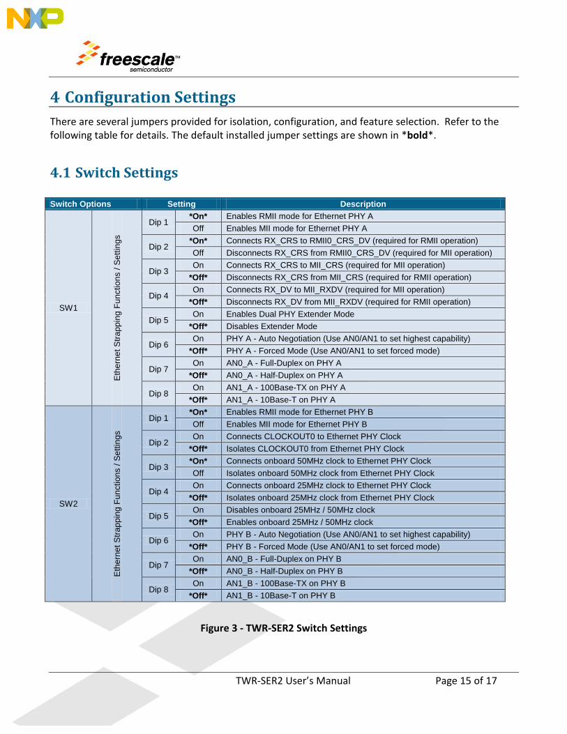
There are several jumpers provided for isolation, configuration, and feature selection. Refer to the following table for details. The default installed jumper settings are shown in *bold*.
4.1 Switch Settings Switch Options Setting Description
SW1
Eth
ern
et
Str
ap
pin
g F
un
ctio
ns /
Se
ttin
gs
Dip 1 *On* Enables RMII mode for Ethernet PHY A
Off Enables MII mode for Ethernet PHY A
Dip 2 *On* Connects RX_CRS to RMII0_CRS_DV (required for RMII operation)
Off Disconnects RX_CRS from RMII0_CRS_DV (required for MII operation)
Dip 3 On Connects RX_CRS to MII_CRS (required for MII operation)
*Off* Disconnects RX_CRS from MII_CRS (required for RMII operation)
Dip 4 On Connects RX_DV to MII_RXDV (required for MII operation)
*Off* Disconnects RX_DV from MII_RXDV (required for RMII operation)
Dip 5 On Enables Dual PHY Extender Mode
*Off* Disables Extender Mode
Dip 6 On PHY A - Auto Negotiation (Use AN0/AN1 to set highest capability)
*Off* PHY A - Forced Mode (Use AN0/AN1 to set forced mode)
Dip 7 On AN0_A - Full-Duplex on PHY A
*Off* AN0_A - Half-Duplex on PHY A
Dip 8 On AN1_A - 100Base-TX on PHY A
*Off* AN1_A - 10Base-T on PHY A
SW2
Eth
ern
et
Str
ap
pin
g F
un
ctio
ns /
Se
ttin
gs
Dip 1 *On* Enables RMII mode for Ethernet PHY B
Off Enables MII mode for Ethernet PHY B
Dip 2 On Connects CLOCKOUT0 to Ethernet PHY Clock
*Off* Isolates CLOCKOUT0 from Ethernet PHY Clock
Dip 3 *On* Connects onboard 50MHz clock to Ethernet PHY Clock
Off Isolates onboard 50MHz clock from Ethernet PHY Clock
Dip 4 On Connects onboard 25MHz clock to Ethernet PHY Clock
*Off* Isolates onboard 25MHz clock from Ethernet PHY Clock
Dip 5 On Disables onboard 25MHz / 50MHz clock
*Off* Enables onboard 25MHz / 50MHz clock
Dip 6 On PHY B - Auto Negotiation (Use AN0/AN1 to set highest capability)
*Off* PHY B - Forced Mode (Use AN0/AN1 to set forced mode)
Dip 7 On AN0_B - Full-Duplex on PHY B
*Off* AN0_B - Half-Duplex on PHY B
Dip 8 On AN1_B - 100Base-TX on PHY B
*Off* AN1_B - 10Base-T on PHY B
Figure 3 - TWR-SER2 Switch Settings

TWR-SER2 User’s Manual Page 16 of 17
4.2 Jumper Settings Jumper Options Setting Description
J1 RS232/485 RX Select (UART 1) 1-2 RS485 Mode (connects RX to RO)
*2-3* RS232 Mode (connects RX to R1OUT)
J2 RS232/485 TX Select (UART 1) 1-2 RS485 Mode (connects TX to DI)
*2-3* RS232 Mode (connects TX to T1IN)
J4 CAN Isolation
1-2 Connects CAN_S to S
3-4 Connects CAN_TX to TXD
5-6 Connects CAN_RX to RXD
J7 JS16 RS232 Isolation (UART 0) *1-2* Connects RX to S08JS16 RXD
*3-4* Connects TX to S08JS16 TXD
J8 Power Down Port B 1-2 Disables Ethernet PHY B
J9 Power Down Port A 1-2 Disables Ethernet PHY A
J11 RS485 Config (UART 1)
1-2 Loopback Mode (connects RE to DE)
3-4 Loopback Mode (connects TX0_P to RX0_P)
5-6 Loopback Mode (connects TX0_N to RX0_N)
7-8 NC
9-10 5V Supply to DB9
J13 RS232/485 Disable (UART 1) *1-2* Disables RS485
2-3 Disables RS232
J16 VBUS OC Isolation 1-2 Connects USB VBUS OC to Elevator
J21 VBUS EN Isolation 1-2 Connects USB VBUS EN to Elevator
J22 RS232 (UART2) Isolation
1-2 Connects TX to T1IN
3-4 Connects RX to R1OUT
5-6 Connects RTS to T2IN
7-8 Connect CTS to R2OUT
J23 RS232 (UART3) Isolation
1-2 Connects TX to T1IN
3-4 Connects RX to R1OUT
5-6 Connects RTS to T2IN
7-8 Connects CTS to R2OUT
J24 USB Device Mode 1-2 Device Mode (capable of powering Tower System)
Figure 4 - TWR-SER2 Jumper Settings

TWR-SER2 User’s Manual Page 17 of 17
5 Mechanical Form Factor
The TWR-SER2 is designed for the Freescale Tower System as a side mounting peripheral and complies with the electrical and mechanical specification as described in Freescale Tower Electromechanical Specification.
Freescale™ and the Freescale logo are trademarks of
Freescale Semiconductor, Inc. All other product or service names
are the property of their respective owners.
© Freescale Semiconductor, Inc. 2009. All rights reserved.