Embed Size (px)
Citation preview

Microelectronics Reliability 78 (2017) 243–248
Contents lists available at ScienceDirect
Microelectronics Reliability
j ourna l homepage: www.e lsev ie r .com/ locate /microre l
Transition voltage of AlGaN/GaN heterostructure MSM varactor withtwo-dimensional electron gas
J. Osvald a,⁎, G. Vanko a, L. Chow b, N.C. Chen c, L.B. Chang d,e,f
a Institute of Electrical Engineering, Slovak Academy of Sciences, Dúbravská cesta 9, 841 04 Bratislava, Slovakiab Department of Physics, University of Central Florida, Orlando, FL 32816-2385, USAc Graduate Institute of Electro-Optical Engineering, Chang Gung University, Tao-Yuan 333, Taiwand Institute of Electro-Optical Engineering, Green Technology Research Center, Chang Gung University, Tao-Yuan 333, Taiwane Ming Chi University of Technology, New Taipei City 243, Taiwanf Department of Otolaryngology Head and Neck Surgery, Chang Gung Memorial Hospital, Taoyuan 333, Taiwan
⁎ Corresponding author.E-mail address: [email protected] (J. Osvald).
http://dx.doi.org/10.1016/j.microrel.2017.09.0040026-2714/© 2017 Elsevier Ltd. All rights reserved.
a b s t r a c t
a r t i c l e i n f oArticle history:Received 9 May 2017Received in revised form 4 September 2017Accepted 4 September 2017Available online xxxx
It is not in principle clear which of the capacitors forming a varactor is responsible for the capacitance change atthe transition voltage. We analyzed a theoretical case of transition voltage of the varactor formed by idealSchottky diodes. Since real devices often do not behave strictly according to thermionic theory we also analyzedthe transition voltage of experimental metal-semiconductor-metal (MSM) varactor with a two-dimensionalelectron gas and an MSM varactor with a dielectric layer. We found that the transition voltage of the MSMvaractor was determined by the reverse-biased diode of the varactor. A voltage drop on the forward-biaseddiode was too low to spill over electrons in the AlGaN layer and to reduce the capacitance of the structure. Thetransition voltage of the MSM varactor was therefore very close to – the threshold voltage of the single diode.The situation was different with the MSM varactor with higher leakage current or in MSM varactor with the di-electric layer. The voltage drop on the forward-biased diode is no more negligible and both parts of the varactorwere polarized by voltage drops on them that were caused by direct current flow. In this case, the transition volt-age of the varactor was enhanced by the voltage drop on the forward-biased diode. Since the transition voltagedetermines the voltage region inwhich the varactor protect circuit devices connected in series to the varactor thepresented results may help to tune this voltage region.
© 2017 Elsevier Ltd. All rights reserved.
Keywords:MSM varactorTransition voltage of MSM varactorVoltage surge
1. Introduction
The varactor as a voltage dependent capacitor is widely applied inoscillators, filters and frequency multipliers [1,2]. Its undisputable ad-vantage is the ability to be directly integrated with other active semi-conductor devices. The same is true for AlGaN/GaN-based varactorswith a two-dimensional electron gas (2DEG), which is a very conve-nient structure for RF devices [3]. Varactors are, for example, used toprotect another device in a circuit against voltage surge [4,5]. The degreeof protection is related to the capacitance swing that is an important pa-rameter of the varactor and is defined as the ratio between the high andthe low capacitance of the varactor. A metal-semiconductor-metal(MSM) varactor consists of two Schottky diodes that are connectedback to back. Application of III–V heterostructures with a 2DEG invaractors allows for deviceswith awider capacitance swing. The voltageswing of the varactor, which defines the voltage range over which a de-vice connected in series with the varactor is protected against voltage
surges, is an interesting parameter [6]. However, experimental resultsshow that technological treatment [7] changes the properties and thevoltage width of the varactor only slightly.
Similarly, as in a metal-insulator-semiconductor heterojunctionfield-effect transistor (MISHFET), a thin dielectric layer inserted be-tween themetal gate and the AlGaN barrier layer should reduce leakagecurrentflowing through the device [8–10]. However, as it will be shownfurther, the dielectric layer also reduces the forward current [11], whichhas a final impact on the transition voltage of the varactor. In this paper,we analyze factors that influence the transition voltage of an MSMvaractor and anMSM varactor with an insulating layer – a metal insula-tor semiconductor heterojunction (MISH) varactor.
Under increasing external bias, the varactor capacitance drops froma plateau value when one of the capacitances connected in series dropsdown. The transition voltage from the high to the low capacitance of areverse-biased diode of the varactor depends on the Schottky barrierheight, doping concentration of the AlGaN layer, AlGaN layer thicknessand on Al mole fraction which is connected with the value of the polar-ization charge [12]. The transition voltage of the forward bias region de-pends principally on the same parameters. The bias voltage for the

244 J. Osvald et al. / Microelectronics Reliability 78 (2017) 243–248
varactor capacitance drop was studied in [13]. Marso et al. [14] foundthat the transition voltage is divided between the two diodes with a~4.1 V voltage drop on the reverse-biased diode and 0.9–1 V on the for-ward-biased one. It means theoretically that the reason for the capaci-tance transition of the varactor may be either the capacitancetransition of the reverse-biased diode or that of the forward-biaseddiode. We study factors influencing the transition voltage of MSM andMISHFET varactors. While there are several experimental and theoreti-cal investigations of different types of varactor, it appears that no circuitsimulation of the transition voltage of varactors has yet been developed.This paper reports on a simulation study and experimental results eluci-dating factors that influence the transition voltage ofMSMandMISHFETvaractors.
2. Theory and experiment
Two Schottky diodes connected back to back which form thevaractor divide external voltage to voltage drops on the forward-biaseddiode and the reverse-biased diode. Because of a higher resistance of thereverse-biased diode, the voltage drop is higher on this diode. It is clearthat the capacitance of the diodes connected back to back may, in prin-ciple, decrease either if the voltage drop on the reverse-biased diodereaches the value at which its capacitance decreases or the voltagedrop on the forward-biased diode reaches a much lower value wherethe forward bias diode capacitance vanishes because of the spill-overof electrons into the AlGaN layer.
For ametal semiconductor diode, the thermionic current density as afunction of voltage is
J ¼ J0 expqVnkT
� �−1
� �; ð1Þ
where n is an ideality factor of the diodes and
J0 ¼ A��T2 exp −qϕkT
� �ð2Þ
Fig. 1.View and the cross-section of the two Schottky gate capacitors forming the varactor. G is
is the saturation current density and φ is the barrier height. The voltagedrops on single diodes are [15]
V1 ¼ nkTq
lnJJ0
þ 1� �
; ð3Þ
for the forward-biased diode and
V2 ¼ −nkTq
ln −JJ0
þ 1� �
; ð4Þ
for the reverse-biased diode. The whole applied voltage is the
V ¼ V1 þ V2 ¼ nkTq
lnJJ0
þ 1� �
− ln −JJ0
þ 1� �� �
: ð5Þ
We studied experimentally an MSM varactor prepared on anAl0.25Ga0.75N/GaN heterostructure grown on 350 μm thick silicon sub-strate. In contrary to previous studies, we used device topology whichenabled us to measure separately electrical properties of the single di-odes of the varactor. A schematic view of the experimental structure isshown in Fig. 1. A circular topology of HEMT (C-HEMT) was used. Thesource/drain Ohmic contacts were formed using a Nb/Ti/Al/Ni/Au me-tallic system, alloyed at 850 °C for 35 s. Sequential electron beam evap-oration of an Ir/Al gatemultilayer (7 periods of Ir/Al) followed by a top Irlayer and lift-off were carried out subsequently to form 120 nm thickring gate contacts of variable area. The Schottky contact of ourmeasureddiode is formed by the electrode G (gate) and the Ohmic contact by theelectrode D (drain) of the transistor structure. The varactor characteris-tics are measured between G electrodes of the diodes. The distance be-tween the diodes forming the varactor was typically 2 mm.
Wemeasured I-V and C-V curves at a frequency of 1MHz of HFET ca-pacitors between the gate and the drain of the transistor structure andthe source was left floating. Varactor structures were measured be-tween two neighbouring Schottky gates. We also studied an MSMvaractor with the dielectric layer under the metal gate – analogous toa MISHFET. Therefore, we prepared metal-insulator-semiconductor
the Schottky gate and D is theOhmic contact. Varactor is formed between the G electrodes.
245J. Osvald et al. / Microelectronics Reliability 78 (2017) 243–248
(MISH) capacitors, too. The topology of the structures was the same asthat of the HFET MSM varactor. The heterostructure was prepared byMO CVD technique. The thickness of the AlGaN layer with an Al molefraction of 25% was 25 nm and that of Al2O3 was 20 nm, and the layerwas deposited by atomic layer deposition (ALD). The gate was formedusing Ni/Au metallization, and the used gate area of the MSM varactorand MSM varactors with the dielectric layer was 9.42 × 10⁻⁴ and1.32 × 10−3 cm2. Concentration of the 2DEG was 6 × 1012 cm−2
and electron mobility 2300 cm2 V−1 s−1. The doping concentrationof AlGaN and GaN layers were estimated from a simulation to be1 × 1015 and 1 × 1016 cm−3, respectively.
3. Results and discussion
3.1. MSM varactor
The above-mentioned equations enable us to construct I-V charac-teristics of the single diodes and also the I-V characteristics of thewhole varactor. Fig. 2 shows simulated I-V curves of varactors withSchottky barrier heights of 1.4 and 1.26 V. These barrier height werechosen since experimental diodes have such barriers as is shown later.In the case of the 1.4 V barrier height, two different diode ideality factors
Fig. 2. I-V curve of a varactor with two back-to-back connected diodes and voltage dropson forward VF and reverse VR biased diodes for a) Schottky barrier height φ = 1.4 V andideality factor n = 1 and b) φ = 1.4 V and ideality factor n = 3 and c) φ = 1.26 V andideality factor n = 3.4.
were considered. Besides the I-V curve of thewhole structure, simulatedvoltage drops on the forward- and reverse-biased diodes are alsoshown. It is shown that for both barrier heights the voltage drop onthe forward-polarized diode in the varactor is negligible comparedwith that of the reverse-polarized diode. For the forward-polarizeddiode, the voltage reaches ~0.02 V, and it does not increase furthersince the current is limited by the saturation current. This valuewas cal-culated for the Schottky diode with a unity ideality factor. For non-idealthermionic transportwith a higher ideality factor (n=3or n=3.4), thevoltage drop on the forward-biased diode may be higher but still below0.05 V.
This calculated value of the voltage drop on the forward-biaseddiode is lower than the value of ~1 V assessed in Ref. [14], which isthe voltage at which the capacitance of the forward-biased AlGa/GaNheterostructure vanishes. Our results show that the transition voltageof the Schottky diode varactor should be practically the same as thethreshold voltage of the corresponding HEMT transistor. Merely this istrue for Schottky diode contact with no or negligible leakage currentof the diode. Unlike the transistor with one Schottky contact and oneOhmic contact, the Schottky diode varactor had only two identicalSchottky contacts and no Ohmic contact.
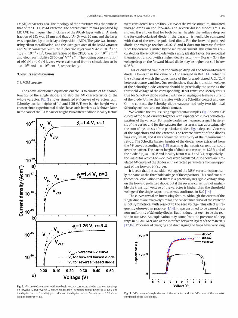
We verified the results using experimental samples. Fig. 3 shows C-Vcurves of theMSMvaractor togetherwith capacitance curves of both ca-pacitors of the varactor. For single diodes wemeasured a small hystere-sis of the curves and for the varactor the hysteresis was approximatelythe sum of hysteresis of the particular diodes. Fig. 4 depicts I-V curvesof the capacitors and the varactor. The reverse current of the diodeswas very small, and it was below the sensitivity of the measurementset-up. The Schottky barrier heights of the diodes were extracted fromthe I-V curves according to [16] assuming thermionic current transportover the barrier. The barrier height of diode onewas φ1 = 1.26 V and ofthe diode 2 φ2 = 1.40 V and ideality factor n=3 and 3.4, respectively -the values forwhich the I-V curveswere calculated. Also shown are sim-ulated I-V curves of the diodeswith extracted parameters fromanupperpart of the forward I-V curves.
It is seen that the transition voltage of theMSM varactor is practical-ly the same as the threshold voltage of the capacitors. This confirms ourtheoretical calculation that there is a practically negligible voltage dropon the forward polarized diode. But if the reverse current is not negligi-ble the transition voltage of the varactor is higher than the thresholdvoltage of the single capacitors, as was confirmed in Ref. [14].
The curves reveal an interesting feature. Although the curves of thesingle diodes are relatively similar, the capacitance curve of the varactoris not symmetrical with respect to the zero voltage. This effect is fre-quently observed in practice [1,14]. It was assumed to be caused by anon-uniformity of Schottky diodes. But this does not seem to be the rea-son in our case. An explanation may come from the presence of deeptraps in AlGaN, GaN, and at the interface between layers of thematerials[17,18]. Processes of charging and discharging the traps have very long
Fig. 3. C-V curves of single diodes of the varactor and the C-V curve of the varactorcomposed of the two diodes.
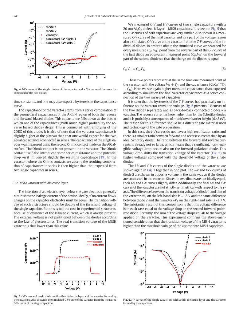
Fig. 4. I-V curves of the single diodes of the varactor and a C-V curve of the varactorcomposed of the two diodes.
246 J. Osvald et al. / Microelectronics Reliability 78 (2017) 243–248
time constants, and onemay also expect a hysteresis in the capacitancecurve.
The capacitance of the varactor stems from a series combination ofthe geometrical capacitances of the AlGaN region of both the reverseand forward biased diodes. This capacitance falls down at the bias atwhich one of the capacitances (with much higher probability the re-verse biased diode) drops. This is connected with emptying of the2DEG of this diode. It is also of note that the varactor capacitance isslightly higher at the plateau than that one would expect for the twoequal capacitances connected in series. The capacitance of the single di-odeswasmeasured using the secondOhmic contactmade on the AlGaNsurface. The Ohmic contact is not present in the varactor. The Ohmiccontact itself also introduced some series resistance and the potentialdrop on it influenced slightly the resulting capacitance [19]. In thevaractor, where the Ohmic contacts are absent, the resulting combina-tion of capacitances in series is then higher than that expected fromtwo single capacitors in series.
3.2. MSM varactor with dielectric layer
The insertion of a dielectric layer below the gate electrode generallydiminishes the leakage current of the device. Ideally, if no current flows,charges on the capacitor electrodes must be equal. The transition volt-age of such a structure should be double of the threshold voltage ofthe single capacitor. But this is not the case in experimental structures,because of existence of the leakage current, which is always present.The external voltage is not partitioned between the diodes accordingto the law of electrostatics. The real transition voltage of the MISHvaractor is thus lower than this value.
Fig. 5. C-V curves of single diodes with a thin dielectric layer and the varactor formed bythe capacitors. Also shown is the simulated C-V curve of the varactor from the measuredC-V curves of the single capacitors.
We measured C-V and I-V curves of two single capacitors with a20 nm Al2O3 dielectric layer – MISH capacitors. It is seen in Fig. 5 thatthe C-V curves of both capacitors are very similar. Also shown is a mea-sured C-V curve of the final varactor and in a part of the voltage regionalso a simulated C-V curve of the varactor from the C-V curves of the in-dividual diodes. In order to obtain the simulated curve we searched forevery measured (Ci1,Vi1) point from the reverse part of the C-V curve ofthe first diode an equivalent measured point (Cj2,Vj2) on the forwardpart of the second diode so, that the charge on the diodes is equal
Ci1Vi1 ¼ C j2V j2: ð6Þ
These two points represent at the same time onemeasured point ofthe varactor with the voltage Vi1 + Vj2 and the capacitance (Ci1Cj2)/(Ci1+ Cj2). Here we see again higher measured capacitance than expectedaccording to simulation the final varactor capacitance as a series con-nection of the two measured capacitors.
It is seen that the hysteresis of the C-V curves had practically no in-fluence on the varactor transition voltage. Fig. 6 presents I-V curves ofthe two diodes separately and as back-to-back connected diodes – avaractor. The reverse current is here higher than for the Schottky diodesand it is probably a consequence ofmuch lower barrier height (0.48 eV).The reason for this difference should be a different gate material usedand technology of the gate preparation.
In this case, the I-V curves do not have a high rectification ratio, andthere is a smaller ratio between forward and reverse currents thanby anideal Schottky diode. The ratio between the forward and reverse cur-rents is already not so large, which means that a significant, non-negli-gible, voltage drop occurs also on the forward-polarized diode. Thisvoltage drop shifts the transition voltage of the varactor (Fig. 5) tohigher voltages compared with the threshold voltage of the singlediodes.
The I-V and C-V curves of the single diodes and the varactor areshown again in Fig. 7 together in one plot. The I-V and C-V curves ofdiode 2 are shown in opposite voltage in the same way as if the diodesare connected in the varactor. Since the two diodes are not ideally equal,their I-V and C-V curves slightly differ. Additionally, the final I-V and C-Vcurves of the varactor are not strictly symmetrical with respect to the y-axis. The difference between the transition voltage of diode 1 and that ofthe varactor δV1 on the left-hand side is ~1.5 V and the same differencebetween diode 2 and the varactor δV2 on the right-hand side is ~1.7 V.The substantial result of this comparison is that this voltage differenceis in each case equal to the voltage drop on the second forward-polar-ized diode. Certainly, the sum of the voltage drops equals to the voltageapplied on the varactor. This experiment confirms the above-men-tioned consideration that the transition voltage of the MISH varactor ishigher than the threshold voltage of the appropriate MISH capacitors.
Fig. 6. I-V curves of the single capacitors with a thin dielectric layer and the varactorformed by the capacitors.
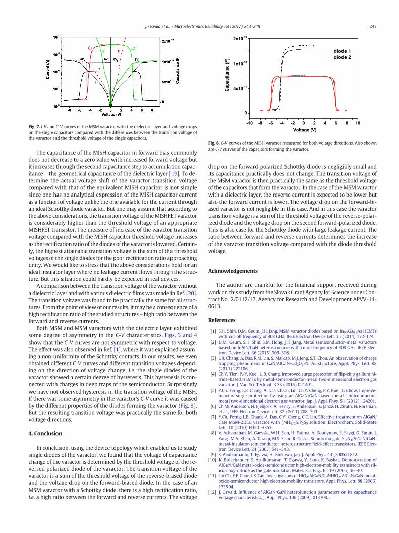
Fig. 7. I-V and C-V curves of the MSM varactor with the dielectric layer and voltage dropson the single capacitors compared with the differences between the transition voltage ofthe varactor and the threshold voltage of the single capacitors.
Fig. 8. C-V curves of the MISH varactor measured for both voltage directions. Also shownare C-V curves of the capacitors forming the varactor.
247J. Osvald et al. / Microelectronics Reliability 78 (2017) 243–248
The capacitance of the MISH capacitor in forward bias commonlydoes not decrease to a zero value with increased forward voltage butit increases through the second capacitance step to accumulation capac-itance – the geometrical capacitance of the dielectric layer [19]. To de-termine the actual voltage shift of the varactor transition voltagecompared with that of the equivalent MISH capacitor is not simplesince one has no analytical expression of the MISH capacitor currentas a function of voltage unlike the one available for the current throughan ideal Schottky diode varactor. But onemay assume that according tothe above considerations, the transition voltage of theMISHFET varactoris considerably higher than the threshold voltage of an appropriateMISHFET transistor. The measure of increase of the varactor transitionvoltage compared with the MISH capacitor threshold voltage increasesas the rectification ratio of the diodes of the varactor is lowered. Certain-ly, the highest attainable transition voltage is the sum of the thresholdvoltages of the single diodes for the poor rectification ratio approachingunity. Wewould like to stress that the above considerations hold for anideal insulator layer where no leakage current flows through the struc-ture. But this situation could hardly be expected in real devices.
A comparison between the transition voltage of the varactorwithouta dielectric layer andwith various dielectric filmswasmade in Ref. [20].The transition voltage was found to be practically the same for all struc-tures. From the point of view of our results, it may be a consequence of ahigh rectification ratio of the studied structures – high ratio between theforward and reverse currents.
Both MSM and MSM varactors with the dielectric layer exhibitedsome degree of asymmetry in the C-V characteristics. Figs. 3 and 4show that the C-V curves are not symmetric with respect to voltage.The effect was also observed in Ref. [1], where it was explained assum-ing a non-uniformity of the Schottky contacts. In our results, we evenobtained different C-V curves and different transition voltages depend-ing on the direction of voltage change, i.e. the single diodes of thevaractor showed a certain degree of hysteresis. This hysteresis is con-nected with charges in deep traps of the semiconductor. Surprisinglywe have not observed hysteresis in the transition voltage of the MISH.If there was some asymmetry in the varactor's C-V curve it was causedby the different properties of the diodes forming the varactor (Fig. 8).But the resulting transition voltage was practically the same for bothvoltage directions.
4. Conclusion
In conclusion, using the device topology which enabled us to studysingle diodes of the varactor, we found that the voltage of capacitancechange of the varactor is determined by the threshold voltage of the re-versed polarized diode of the varactor. The transition voltage of thevaractor is a sum of the threshold voltage of the reverse-biased diodeand the voltage drop on the forward-biased diode. In the case of anMSM varactor with a Schottky diode, there is a high rectification ratio,i.e. a high ratio between the forward and reverse currents. The voltage
drop on the forward-polarized Schottky diode is negligibly small andits capacitance practically does not change. The transition voltage ofthe MSM varactor is then practically the same as the threshold voltageof the capacitors that form the varactor. In the case of theMSM varactorwith a dielectric layer, the reverse current is expected to be lower butalso the forward current is lower. The voltage drop on the forward-bi-ased varactor is not negligible in this case. And in this case the varactortransition voltage is a sumof the threshold voltage of the reverse-polar-ized diode and the voltage drop on the second forward-polarized diode.This is also case for the Schottky diode with large leakage current. Theratio between forward and reverse currents determines the increaseof the varactor transition voltage compared with the diode thresholdvoltage.
Acknowledgements
The author are thankful for the financial support received duringwork on this study from the SlovakGrant Agency for Science under Con-tract No. 2/0112/17, Agency for Research and Development APVV-14-0613.
References
[1] S.H. Shin, D.M. Geum, J.H. Jang, MSM varactor diodes based on In0.7Ga0.3As HEMTswith cut-off frequency of 908 GHz, IEEE Electron Device Lett. 35 (2014) 172–174.
[2] D.M. Geum, S.H. Shin, S.M. Hong, J.H. Jang, Metal semiconductor-metal varactorsbased on InAlN/GaN heterostructure with cutoff frequency of 308 GHz, IEEE Elec-tron Device Lett. 36 (2015) 306–308.
[3] L.B. Chang, A. Das, R.M. Lin, S. Maikap, M.J. Jeng, S.T. Chou, An observation of chargetrapping phenomena in GaN/AlGaN/Gd2O3/Ni-Au structure, Appl. Phys. Lett. 98(2011) 222106.
[4] Ch.Y. Tien, P.-Y. Kuei, L,.B. Chang, Improved surge protection of flip-chip gallium ni-tride-based HEMTs by metal-semiconductor-metal two-dimensional electron gasvaractor, J. Vac. Sci. Technol. B 33 (2015) 021401.
[5] Y.Ch. Ferng, L.B. Chang, A. Das, Ch.Ch. Lin, Ch.Y. Cheng, P.Y. Kuei, L. Chow, Improve-ment of surge protection by using an AlGaN/GaN-based metal-semiconductor-metal two-dimensional electron gas varactor, Jap. J. Appl. Phys. 51 (2012) 124201.
[6] Ch.M. Anderson, N. Ejebjörk, A. Henry, S. Andersson, E. Janzé, H. Zirath, N. Rorsman,et al., IEEE Electron Device Lett. 32 (2011) 788–790.
[7] Y.Ch. Ferng, L.B. Chang, A. Das, C.Y. Cheng, C.C. Lin, Effective treatment on AlGaN/GaN MSM-2DEG varactor with (NH4)2S/P2S5 solution, Electrochem. Solid-StateLett. 10 (2010) H350–H353.
[8] V. Adivarahan, M. Gaevski, W.H. Sun, H. Fatima, A. Koudymov, S. Saygi, G. Simin, J.Yang, M.A. Khan, A. Tarakji, M.S. Shur, R. Gaska, Submicron gate Si3N4/AlGaN/GaN-metal-insulator-semiconductor heterostructure field-effect transistors, IEEE Elec-tron Device Lett. 24 (2003) 541–543.
[9] S. Arulkumaran, T. Egawa, H. Ishikawa, Jap. J. Appl. Phys. 44 (2005) L812.[10] K. Balachander, S. Arulkumaran, T. Egawa, Y. Sano, K. Baskar, Demonstration of
AlGaN/GaN metal-oxide-semiconductor high-electron-mobility transistors with sil-icon oxy-nitride as the gate insulator, Mater. Sci. Eng., B 119 (2005) 36–40.
[11] Liu Ch, E.F. Chor, L.S. Tan, Investigations of HfO2/AlGaN/GaNHfO2/AlGaN/GaNmetal-oxide-semiconductor high electron mobility transistors, Appl. Phys. Lett. 88 (2006)173504.
[12] J. Osvald, Influence of AlGaN/GaN heterojunction parameters on its capacitancevoltage characteristics, J. Appl. Phys. 106 (2009), 013708. .

248 J. Osvald et al. / Microelectronics Reliability 78 (2017) 243–248
[13] M. Marso, M. Wolter, P. Javorka, A. Fox, P. Kordoš, AlGaN/GaN varactor diode for in-tegration in HEMT circuits, Electron. Lett. 37 (2001) 1476–1478.
[14] M. Marso, A. Fox, G. Heidelberger, P. Kordoš, H. Lüth, Comparison of AlGaN/GaNMSM varactor diodes based on HFET and MOSHFET layer structures, IEEE ElectronDevice Lett. 27 (2006) 945–947.
[15] J. Osvald, Back-to-back connected asymmetric Schottky diodes with series resis-tance as a single diode, Phys. Status Solidi A 212 (2015) 2754–2758.
[16] J. Osvald, E. Dobročka, Generalized approach to the parameter extraction from I–Vcharacteristics of Schottky diodes, Semicond. Sci. Technol. 11 (1996) 1198–1202.
[17] P. Dianat, R.W. Prusak, E. Gallo, A. Cola, A. Persano, F. Quarant, B. Nabel, A highly tun-able heterostructure metal-semiconductor-metal capacitor utilizing embedded 2-dimensional charge, Appl. Phys. Lett. 100 (2012) 153505.
[18] J. Osvald, Simulation of the influence of interface states on capacitance characteris-tics of insulator/AlGaN/GaN heterojunctions, Phys. Status Solidi A 210 (2013)1340–1344.
[19] P. Chattopadhyay, B. Ray Chaudhuri, Frequency dependence of forward capacitance-voltage characteristics of Schottky barrier diodes, Solid State Electron. 36 (1993)605–610.
[20] Ch.Y. Tien, P.Y. Kuei, L.B. Chang, Ch.P. Hsu, Capacitance swing and capacitance ratioof GaN-based metal-semiconductor-metal two-dimensional electron gas varactorwith different dielectric films, J. Electr. Eng. Technol. 10 (2015) 1720–1724.