Embed Size (px)
Citation preview

University of South CarolinaScholar Commons
Theses and Dissertations
2016
Simulation Of GaN Based MIS VaractorBojidha BabuUniversity of South Carolina
Follow this and additional works at: http://scholarcommons.sc.edu/etd
Part of the Electrical and Electronics Commons
This Open Access Thesis is brought to you for free and open access by Scholar Commons. It has been accepted for inclusion in Theses and Dissertationsby an authorized administrator of Scholar Commons. For more information, please contact [email protected].
Recommended CitationBabu, B.(2016). Simulation Of GaN Based MIS Varactor. (Master's thesis). Retrieved from http://scholarcommons.sc.edu/etd/3863

SIMULATION OF GAN BASED MIS VARACTOR
by
Bojidha Babu
Bachelor of Engineering
Anna University, 2013
Submitted in Partial Fulfillment of the Requirements
For the Degree of Master of Science in
Electrical Engineering
College of Engineering and Computing
University of South Carolina
2016
Accepted by:
Grigory Simin, Director of Thesis
Guoan Wang, Reader
Paul Allen Miller, Vice Provost and Interim Dean of Graduate Studies

ii
© Copyright by Bojidha Babu, 2016
All Rights Reserved.
iii
DEDICATION
This work is dedicated to my parents who have been my soul support.

iv
ACKNOWLEDGEMENTS
First and foremost my deepest gratitude is to my advisor, Professor Grigory S.
Simin who accepted me as a Masters student in his group. I always felt fortunate to have
him as my research advisor. Under his guidance I have learnt a lot as an individual,
carrying not only a small portion of his vast knowledge and experiences, but also his
optimism and methodology in getting through obstacles, both in research and in life. I do
not have words to thank him for all his support, help and guidance during my time in
University of South Carolina. I would also like to thank chair of Electrical Engineering
department, Professor Roger Dougal for providing me the opportunity to work for my
graduate studies. I am grateful to my Master’s thesis committee member Dr. Guoan Wang
for his support.
Above all, I would like to thank my parents for showering me with their immense support
and love throughout my life.
Finally, I would like to express my gratitude towards my friends for their endless support
and encouragement and for making my stay in Columbia, SC a memorable one.

v
ABSTRACT
This work deals with novel microwave switches based on III-Nitride varactors.
RF switches, power limiters and other control devices are important components of
various RF systems, such as wireless modules of laptops, tablets, cell phones etc.,
satellites communication systems, radars, multi-band wireless and aerospace
communications, phased array antennas and so worth. Traditional RF switches are
fabricated using pin diodes or MEMS, Si MOSFETs or GaAs HEMTs. These devices have
a number of fundamental limitations. Si or GaAs based devices suffer from a low
breakdown voltage and cannot handle high RF power. Pin-diodes require large forward
currents and do not allow for fast turn-on. III-Nitride heterostructures open tremendous
opportunities for RF control devices due to the record high sheet electron density in the
2D channel, extremely low channel resistance, high breakdown field and excellent
temperature stability. Recently, RF switches based on III-Nitride High Electron Mobility
Transistors (HEMTs) have been developed and became commercially available. In this
work, we studied a novel type of RF switch based on III-Nitride varactor. Unlike HEMTs,
varactor uses capacitance modulation to control the flow of RF signal and offers a number
of advantages over HEMTs: they allow for shorter channel, do not have gates or ohmic
contacts and hence the fabrication is alignment- and anneal - free, they do not consume
DC current and provide the DC block. Unlike regular varactor diodes, in this work, we
analyze three-terminal varactor having independent control electrode which further
enhances the switch performance. The varactor and varactor based RF switch analysis in

vi
this work is done by modeling and simulation using Synopsys Sentaurus tools as well as
MATLAB. Modeling approach allows obtaining device characteristics and material
dependencies that are hardly achievable in experiments, such as effect of donor and
acceptor traps or achievable switching time. The obtained results are compared with
available experimental data.

vii
TABLE OF CONTENTS
DEDICATION ................................................................................................................... iii
ACKNOWLEDGEMENTS .................................................................................................... iv
ABSTRACT ....................................................................................................................... v
LIST OF FIGURES ........................................................................................................... viii
CHAPTER 1: INTRODUCTION.............................................................................................. 1
CHAPTER 2: INTRODUCTION TO THREE TERMINAL MIS VARACTOR ................................. 11
CHAPTER 3: MIS VARACTOR AS A RF SWITCH AND ITS C-V CHARACTERISTICS .............. 23
CHAPTER 4: TRANSIENT RESPONSE OF MIS VARACTOR................................................... 40
CHAPTER 5: CONCLUSION ............................................................................................... 52
REFERENCES .................................................................................................................. 54

viii
LIST OF FIGURES
Figure 1.1 RF applications – satellite, radar systems,digital satellite system architecture . 2
Figure 1.2 RF switch-PIN diode, MEMS, solid state switches ......................................... 4
Figure 1.3 GaN HEMT structure, band diagram and working principle representation ..... 8
Figure 2.1 C3 varactor switch ........................................................................................ 13
Figure 2.2 Structure of MIS varactor ............................................................................. 15
Figure 2.3 2D layout of device from Sentaurus .............................................................. 19
Figure 3.1 Representation of MIS varactor structure ...................................................... 25
Figure 3.2 (a) snapshot of eDensity profile at zero bias (b) snapshot of eDensity profile
when negative bias applied between the MIS electrodes and 2DEG channel depleted .... 26
Figure 3.3 a), b) represents the electrostatic profile and c), d) represents space charge
profile at different biasing conditions ............................................................................ 28
Figure 3.4 AC Analysis using Sentaurus ........................................................................ 29
Figure 3.5 CV plot simulated using Sentaurus with varying bias condition .................... 30
Figure 3.6 (a), (b) &(c) CV dependencies of MIS varactor with and without traps ......... 34
Figure 3.7 eDensity profile of MIS Varactor (with & without traps) .............................. 35
Figure 3.8 Insertion loss and isolation of MIS varactor switch compared with experimental
and simulated C3 switch ................................................................................................ 37
Figure 3.9 Isolation and Insertion loss variation with increasing device width ............... 38
Figure 3.10 Isolation and Insertion loss with varying bias conditions ............................. 39
Figure 3.11 Insertion loss with variation in different type of traps .................................. 39
Figure 3.12 Isolation with variation in different type of traps ......................................... 26

ix
Figure 4.1 2D MIS varactor structure ............................................................................ 43
Figure 4.1 Zoomed in figure of the device structure showing the length of metal contact
and electrode spacing .................................................................................................... 44
Figure 4.3 Circuit layout of MIS varactor switch ........................................................... 45
Figure 4.4 Simulated transient response of the MIS varactor switch............................... 47
Figure 4.5 Simulated transient response (with and without traps) ................................... 50
Figure 4.6 eDensity profile of MIS Varactor (with &without traps) during transient
response with varying bias conditions ............................................................................ 51
Figure 4.7 switching time of Schottky C3 varactor Switch; yellow line-applied pulsed
control voltage; blue line-Turn ON (fall time) and Turn OFF (rise time) times .............. 52

1
CHAPTER 1
INTRODUCTION
1.1 Microwave switches
Microwave switches and control devices are key components which can be controlled
electrically to pass, block and redirect electrical signals oscillating at RF frequencies
(electromagnetic spectrum of 300MHz to 30GHz) [3]. They are used in wide range of
applications like radar Tx/Rx modules, software defined radio systems, modern wireless
communication and RF systems. Its importance continuously increases with increase in
their complexity and functionality. Nowadays depending upon the different requirements
of applications various device technologies of microwave switches are available for
commercial use.
Microwave switching and control elements are widely used as a phase shifter in
phased array technology, satellite communications, antennas, radar system, aerospace
communication systems, wireless modules like laptops, tablets, phones etc. Depending on
the type of application frequency range varies from few GHz to 100GHz. Switches with
performance requirements are needed in various application spectrum. These
requirements are dictated by the application systems they are part of, while the concept of
switching remains a common factor. In this microwave switches signal routing is the
main operation which includes selection of single or multiple signals to one output,
selection of signal to one input, transfer switching to add or remove a device from signal
path, matrix switching of inputs and outputs. Such applications require small device area,

1
low insertion loss (less than 1dB), high isolation (greater than 30dB), good linearity, high
operating temperature and low/high power handling capability [1].
Figure 1.1 RF applications – satellite, radar systems,digital satellite system
architecture
1.2 Microwave switch characteristics
Microwave switches achieve high performance in switching and control operation if
they satisfy few basic conditions. First aspect is how well the switch can transfer power
and it is determined by insertion loss. Second aspect is how well the switch can block
power, it is measured by isolation. Insertion loss and isolation evaluate the switch
performance in ON/OFF state. The amount of power lost in the ON state while
transmitting a signal from input port to output port is measured as insertion loss [4]. It is
expressed in dB. It is the ratio of output power delivered to the load at switch’s output
port and input power generated by the signal source.
IL (dB) = - (P out (dBm) – Pin (dBm))
It has an effect by parasitic capacitance, resistance, inductance and conductance present
in the switch. Insertion loss can be expressed via the switch S-parameters:
IL = -20 x log |S21 (ON)|

2
During the matched condition, s-parameter between input and output port of switch
(S21) in ON state is switch’s insertion loss. Isolation is a measure of how output port is
isolated from input port in OFF state. Typically good isolation should be more than 25dB
and should avoid signal from leaking into the desired signal path [4]. It can be defined as
IS = -20 x log |S21 (OFF)|
Third aspect is the maximum power the switch can transfer in ON state and it can
block in OFF state, which is typically defined as point of input power where insertion
loss increases by 1 dB because of the degradation of the switch at extremely high power.
This is called 1 dB power compression point [3]. There are other aspects like return loss,
noise and linearity. While the switch is in ON state the amount of the signal returned or
reflected to source is called return loss (S11). It should be zero (negative infinite in dB
scale) which indicates a perfectly matched condition. Microwave switches have other
important figures of merit like high power handling, fast switching speed, harsh
environment operation and high temperature. Switch isolation degrades over the
frequency range if a single series element acts as a control element. This can be
eliminated by adding a shunt element [3]. During the ON state, shunt element turns OFF
whereas series element remains ON. During the OFF state it is vice versa where shunt
element turns ON and series element turns OFF [4].
1.3 Microwave switch types
Microwave switches can be divided into
Micro Electro Mechanical System (MEMS) switches
Solid state switches

3
MEMS switches use electrostatic induction for the physical movement of highly
conducting thin membrane to turn the switch ON/OFF. It operates at broader bandwidth
(DC to 40 GHz or higher) with high isolation and low insertion loss [5]. However MEMS
switches do not exhibit high signal linearity and high power handling capabilities.
Solid state switches are made up of semiconductor materials in which electronic flow
in the channel turns the switch ON/OFF. Such switching process can be controlled by
applying positive or negative bias. These switches can be either unipolar or bipolar [5]. In
bipolar device (PIN diode) both electrons and holes flow to control switching operation
whereas in unipolar device either holes or electron participate in it. Few examples of
unipolar device switches are CMOS (Complementary Metal Oxide Semiconductor),
GaAs MESFET (Metal Semiconductor Field Effect Transistor), AlGaAs/GaAs HEMT
(High Electron Mobility Transistor) and III-Nitride HEMTs. They are chosen for
applications which require fast switching speed, smaller size, weight and reliability [5].
Figure 1.2 RF switch-PIN diode, MEMS, solid state switches
Due to device design and inadequacies in fundamental material properties these
device have performance limitations like high control voltage, self-actuation, distortions,
reliability issues and low RF power. Expensive MEMS switches have limited operating
life, slow switching time. On the other hand many solid state switches handles only

4
narrow bandwidth with limited operating power and linearity. PIN diodes which acts as a
variable resistor at RF frequencies hold a key role in high power, high frequency
applications but they have disadvantages like large size, longer switch settling time for
higher power operation, require large bias current and their bipolar nature limits the
device switching speed [1]. MEMS (Micro-Electro Mechanical System) operate at 0.1 to
100GHz frequencies. It offers superior performance like low insertion loss (-0.1db up to
40GHz), high isolation, low power consumption, smaller size and weight because it
possess advantages of both electromechanical and semiconductor switches. But it
requires improvements in high power switching, switching speed (2-40us), power
handling, electrostatic discharge tolerance and reliability [1]. For low power applications,
cost effectiveness and advancements in CMOS and silicon on sapphire overruns decades
old GaAs MMIC. Major disadvantages of GaAs technology are low breakdown voltage,
low operating temperature and cannot achieve the required linearity levels due to nature
of the material.
Switching and control applications have demanding performance parameters which
led to newer designs and newer materials like III-Nitrides. GaN MMICs were found to be
promising candidate to replace PIN diodes and MEMS because of their low insertion
loss, high isolation, fast switching speeds, high ESD tolerance and reliability.
1.4 III Nitride RF switches
AlGaN/GaN HFET based RF switch design facilitates as a new exemplar in
microwave switching and control applications. There are numerous advantages of III-
Nitride material over the other materials. GaN semiconductor material has a wide
bandgap of 3.4eV. Unlike other wide bandgap material like SiC they form heterojunction

5
which is an added advantage. Past efforts in III-Nitride devices were mainly power
amplifiers but many improvements in the technology resulted in elimination of surface
breakdown, lower channel and contact resistance, etc.
HFET device forms 2DEG (two dimension electron gas) at the interface of the
heterojunction which has very high record of sheet carrier density and electron mobility
forming a metal like conducting plate [3]. This can be easily controlled to turn on or off
by applying voltage to gate. They have distinctive combination of features like high
breakdown voltage, higher operating temperature, robustness, chemical inertness, very
high RF power, extremely low channel resistance, low off state capacitance, low insertion
loss, high isolation, reliability, fast switching speed and its ability to operate as a planar
structure is excellent for microwave switching and control devices [2]. In comparison
with other material systems, they have high saturation current and thermal conductivity
[2]. This is an ideal material for high power and high frequency applications because of
its higher number in Johnson’s figure of merit. Further developments in device design
like insulated gate HFET (MOSHFET) enables reliability, robust RF switch with ultra-
low control power and high linearity. Such RF switches can work with 10 – 100 times
higher power RF signal than compared to RF MEMS or GaAs HEMT. They are reliable
and thermally stable even at cryogenic temperatures up to 300°C or higher due to their
low intrinsic carrier concentration [2]. Lower power consumption and switching speed
are prominent by two-three orders of magnitude when compared to PIN diodes. Thus
such materials are preferred in RF systems for higher efficiency.
These III-Nitride materials exhibit strong polarization. Polarization in AlGaN/GaN
heterojunction is of two types, i.e. spontaneous and piezoelectric polarization. In GaN

6
there is a difference in electronegativity between the Gallium and Nitrogen in the atomic
layer which results in spontaneous polarization pointing from Ga-face to N-face. Due to
difference in the lattice constants between the AlGaN and GaN layers in the
heterojunction piezoelectric polarization occurs [3]. There is a mechanical strain when
the AlGaN layer stretches over GaN due to which atoms are forced to shift from their
electrically neutral positions giving rise to piezoelectric polarizations. Both the
piezoelectric and spontaneous polarization can be oriented in the same direction by
controlling the growth parameters, Al concentration and layer thickness. This enhances
the total effective polarization charge which attracts the numerous free electrons at the
heterojunction creating 2EG in the channel [3]. 2DEG forms a thin sheet where the
concentration of electrons is really high ~ 2 x 10¹³
cm-2
. It is coupled with trapped
positive charges in the AlGaN layer.
Similar to FET (Field effect transistor), AlGaN/GaN HFET is also a three terminal
voltage control device. Source and drain forms ohmic contacts to 2DEG and gate
terminal is a schottky contact. Current flows in the channel from source to drain contact
and it is controlled by bias voltage applied to the gate terminal. DC and/or RF path is
formed between input and output when a signal is applied to at the input [4]. These
AlGaN/GaN HFETs generally are ON devices, even at zero gate bias the transistor is in
ON state. When a negative bias is applied to the gate the net negative charge on the gate
electrode starts depleting the channel under it. Typical threshold values of HFETs are -4V
[4]. If the applied negative gate voltage is less than the device threshold voltage (Vg<Vth)
then the channel under the gate electrode is completely depleted. This depletion indicates
that the signal path is completely cut off which means the device is said to be in OFF

7
state and it starts behaving like a capacitor. For power applications gate should be placed
close to the source and for microwave switching more than one gate can be used yet
geometry should be symmetrical. Conventionally the gate electrodes are schottky
contacts in HFET but in order to reduce the gate leakage current the design of the device
was slightly modified [4]. This led to the development of insulated gate technologies in
the HFETs called metal oxide semiconductor heterojunction field effect transistor
(MOSHFET) and metal insulator semiconductor heterojunction field effect transistor
(MISHFET). Typical threshold values of MOSHFETs are -8V [6].
Figure 1.3 GaN HEMT structure, its band diagram and working principle
representation

8
When HFETs are used as microwave switches, during ON state the channel resistance
and the two contact resistance of the device are used to calculate the insertion loss
whereas during OFF state the isolation is determined by the capacitance. In order to
achieve efficient switch performance the product of RON*COFF should be minimum [4].
ON resistance (RON) can be reduced only by improving growth quality and device
fabrication process. Improvements in the design layout can reduce OFF capacitance
(COFF). Research and studies demonstrate that COFF decreases with increase in number of
gates. Multigate device design has proven to be having maximum switching power and
increased isolation.
1.5 Limitations of III Nitride RF HFET switches
AlGaN/GaN based HFET have two major limitations in material properties and
device design which is a hindrance to further developments.
First limitation is due to material properties and it deals with ohmic contacts on the
device. In AlGaN/GaN HFET source and drain (input and output) electrodes are ohmic
contacts. Unlike heavy doping in Si, ohmic contact on AlGaN is formed by quickly
annealing a stack of specific metal layers at very high temperature, usually at 800°C to
900°C for less than a minute [4]. AlGaN has a very wide band gap and tough chemical
nature so doping is not an easy task. Rapid thermal Annealing (RTA) is a process to form
ohmic contact on AlGaN. Ti layer in the metal stack plays a key role in this RTA process.
At high temperature Ti anneals and react with AlGaN to form TiN clusters. This leads to
the creation of N vacancies in the AlGaN layer which behave like n-type dopant to
increase conductivity in the affected region. This penetration goes up to several tens of

9
nanometers and it almost reaches the heterojunction interface where the 2DEG channel is
available [3]. Low temperature or short annealing is not enough for effective penetration
similarly very high temperature or short annealing will destroy the 2DEG. High
temperature annealing process possess limits to fabrication steps and device design. It
degrades the device’s morphological quality like surface roughening and area expanding
which results in the increased RF resistivity and decreased critical breakdown voltage [4].
So the annealing condition is controlled carefully to achieve optimum conductivity.
Ohmic contact can only be added in the beginning of the fabrication due to its high
temperature requirement and also requires a separate mask [4].
Second one is due to device design and related to the gate electrode of the device.
Low loss FET microwave switch needs large device periphery with multi finger structure.
There exists technological challenges for the structure with long and zigzagging gate
alignment. In order to maintain the device yield the gate-drain and gate-source spacing is
kept above certain distance to tolerate the alignment error issue which ultimately leads to
additional channel length [4]. The presence of gate leads to additional source-gate and
gate-drain parasitic capacitive coupling. This occurs between RF input and output
through the metal gate which limits the isolation. To avoid premature breakdown in high
power switches the source-gate and gate-drain spacing is sufficiently high. This means
additional channel length is included which leads to higher ON resistance and higher
insertion loss. Studies have proved that existence of the gate is related to 24% of the total
loss [4].

10
In the next chapter a new device design called Capacitively Coupled Contacts (C3)
varactor which was introduced in order to overcome the issues with III-Nitride
technology will be discussed.

11
CHAPTER 2
INTRODUCTION TO THREE TERMINAL MIS VARACTOR
2.1 C3 Varactor
Varactor is a voltage controlled capacitor which has variable capacitance which is a
function of voltage applied across the terminals. Depending on the thickness of the
depletion layer which varies with applied bias voltage the capacitance can be varied.
Thickness of the depletion region is proportional to the square root of the applied voltage
and the capacitance is inversely proportional to the depletion region thickness. So the
capacitance is inversely proportional to the square root of the applied bias voltage.
Among the various devices using GaN technology, the varactor (voltage controlled
capacitor) using 2DEG possess numerous advantages and they play a prominent role in
the microwave switches and control devices. III-Nitride varactors have demonstrated
high performance with significant advantages like high on/off ratio, robustness and
simple gate-alignment-free technology. Our research group collectively combined the
concepts of voltage controlled capacitor (varactor) in GaN based HFET switches and
introduced the GaN based capacitively coupled contact (C3) varactors. Capacitively
coupled contact device design possess higher microwave power handling capability and
low contact resistance when compared to regular HFET devices with annealed ohmic
contact. This concept removes the gate from the device and reduces the overall
impedance which provides higher flexibility to tune the source/drain spacing. Unlike the
transistor switches where the gate is typically designed to accept only the negative bias

12
these varactor switches’ device design is symmetrical so it can be designed to accept
either positive or negative bias to control the device. It does not require DC current flow
through the device instead it generates capacitive coupling effect between metal electrode
and 2DEG to pass the microwave signal. Fig. 2.1 represents the structure of C3 switch.
Figure 2.1 C3 varactor switch
Varactors are preferred over the field-effect transistors for the switching and RF
control applications because of the few main advantages like (i) absence of the gate so
the device forms short channel length as well as gate-alignment free fabrication process
(ii) absence of the ohmic contacts so it eliminates annealing process and structural
damage during fabrication which decreases the edge roughness and increases the
breakdown voltage [4].
Performance limitations
C3 Varactors have certain disadvantages built into the device design which affected
the switch performance. When DC bias is applied between the two RF electrodes of the

13
C3, one of the contacts turns into depletion mode and the other one into accumulation
mode. This limits the OFF-capacitance and hence the achievable isolation. Regular
varactors lack a separate control port, which complicates the biasing circuit and requires
external circuit elements to isolate DC control from the RF path. This two terminal MIS
C3 varactor has a disadvantage where the 2DEG is floating in heterostructure which is
very sensitive to any parasitic crosstalk [3]. This makes it nearly impossible for
fabricating the multi element switch because the potential from the other switches affect
the 2DEG and makes it unstable.
2.2 Three-Terminal MIS Varactor with Capacitively Coupled Contacts
In order to overcome the above varactor limitations, a new device structure is
proposed in this work taking advantage of the C3’s bias dependent impedance. Varactor
design is modified by adding a third electrode. Earlier a three terminal structure called D-
MOSH was proposed but it had and additional ohmic contact as the control electrode [3].
This again involves annealing process and produces structural damage during fabrication
process which decreases the edge roughness and increases the breakdown voltage.
GaN C3 varactors have highly significant leakage current when very high positive or
negative bias is applied as they are conventionally designed with schottky electrodes.
This leakage current limits the performance parameters. Most of the RF control devices
are switches and power limiters where they are large periphery devices. In such a device
or multi element IC the leakage current reaches high value at high temperature while
using the varactors with schottky electrodes. In order to overcome this disadvantage
Metal-Insulator-Heterostructure design was developed. This device design can be used to
reduce the varactor leakage current dramatically but the earlier published works reported

14
that they have hysteresis and trapping effects. These effects compromised the
performance parameters which affected the fast switching factor. Fig. 2.2 represents the
structure of MIS varactor.
Figure 2.2 Structure of MIS varactor
The new design includes a pair of MIS contacts and one Schottky electrode (shown in
the figure). This design is advantageous compared to regular varactor as explained below
Unlike the RF power amplifiers and many other RF systems, RF switches do not require
DC current flowing between the input and output ports. This enables more flexibility in
the switch design. The C3 varactor utilizes the concept of capacitive coupling (a built in
DC block) between the MIS electrodes and the channel beneath to inject RF signal into
the active region. In this device, metal electrodes are deposited on top of a thin dielectric
layer (5nm-10nm) which is placed on the GaN surface which forms the MIS contacts.
This passivation layer reduces potential leakage current when MIS contact is under heavy
bias voltage. Schottky contact is placed on the GaN surface directly. This device does not
need annealing process to deposit the ohmic metal contacts resulting in much lower edge
roughness which further increases the breakdown voltage. The 2DEG channel is
15
modulated with bias and through the movement of free electrons in the channel, the RF
signal is passed from one contact to other. Bias can be applied to either the schottky
contact or the MIS contacts. In order to deplete the channel under the MIS contacts either
positive bias is applied to schottky contact or negative bias is applied to the MIS contacts.
Applying bias creates a negative potential difference between MIS contacts and 2DEG
channel and when the applied bias goes beyond the threshold voltage it results in
depleting the channel. In this way the region under both the MIS contacts are depleted
unlike C3
structure. A RF signal path (active region) is set between the two MIS contacts
and the schottky control electrode is placed outside this RF path so that it does not affect
the insertion loss or isolation which acts similar to a gate contact in the conventional
HFET. Even when a large bias is applied, the active region potential under the MIS
contact remains constant. This reduces the risk of device breakdown under OFF-state and
when there is high signal drop across the switch. The distance between the schottky
control electrode and the MIS contacts (switch’s active region) does not affect the device
performance, so the schottky contact need not be necessarily placed near the MIS
contacts and therefore the device does not require accurate alignment. Absence of gate
has a greater impact on the channel length. The total channel length is more than two
times smaller than in the HFET designed for the same breakdown voltage. This small
channel length makes the resistive part of the MIS impedance is so low (1ohm x mm)
than a typical HFET device whereas the capacitive part is compensated by matching the
circuit. Thus MIS Varactor is a simple, robust, anneal-free, alignment-free fabrication
technology and offers high yield which is compatible with power amplifiers and MMICs
[4].

16
2.3 Three- terminal varactor modeling using Synopsys
In order to predict and estimate device performance, numerical simulation turns out to
be a good method to understand the device physics and behavior of various parameters
like voltages, doping and trap level concentrations. In this thesis a commercial simulator
named Sentaurus which is provided by the company Synopsys is used. Sentaurus is a
Technology Computer Aided Design (TCAD) software which aids in the process of
developing and optimizing the semiconductor processing technologies and devices. It
solves fundamental, physical and partial differential equations to model the structural
properties and electrical behavior of a device structure. The structure is divided into
series of discrete points called mesh. Simulator resolves Poisson equation, continuity
equation of electrons and holes at each point of the mesh. Visualization tools are used to
observe the device structure of 2D models from which various information like carrier
densities, electric field, potential, energy level band gaps, geometrical structure, material
type, doping concentration, electrode properties, temperature, etc. inside the device at
various point of time during simulation can be studied [7].
In this MIS varactor simulation following tools were used: Sentaurus Workbench (a
flexible framework environment with advanced visualization and programmability),
Sentaurus Structure Editor (2D device editor), Sentaurus device (2D device simulator),
and Inspect (visualizing the simulation results like one dimensional functions).
Structure of the device is defined in the following order. Initially the variables are
defined in the files which are later used for the mathematical operations. Further
rectangles or polygons are used to define the regions of the different materials in the

17
device structure. Electrodes are defined and placed at the edges of the device. Finally
mesh is defined by creating windows in the shape of lines, rectangles or polygons.
MIS Varactor consists of one schottky electrode and two MIS electrodes. Barrier
height of the schottky electrode used for this device is 0.7 eV. These electrodes are
placed on top of the GaN cap layer. Si3N4 (Silicon Nitride) passivation layer of 50 nm
thickness is placed on top of the GaN cap layer (except the electrodes region) to reduce
the surface defects (trapping effects). For MIS contacts, Si3N4 passivation layer of 2 nm
thickness is placed in between the metal and the semiconductor (GaN cap) layer. Surface
pinning traps (Donor traps of 5e13 cm-3
at an energy level of 0.4eV from the mid band
gap) are defined between the passivation layer and the GaN cap layer. Electrode length
and the spacing between them is assigned as 1um. Width of the device is defined as 1mm.
Thickness of the top most layer GaN cap is 3 nm and its doping is 5e16 cm-3
. Below
which the AlGaN spacer (2nm) and barrier layer (20nm) with a doping of 2e18 cm-3
is
placed. Polarization at the interface is larger due to which higher electron density is
formed at the interface. A density gradient method is used to include the quantization of
energy level in the quantum well which is formed by the band structure near the interface.
This calculates a better 2DEG of 3-4nm thickness with high carrier density (1e19 cm-3)
in
the GaN channel.

18
Figure 2.3 2D layout of device from Sentaurus
Al mole fraction used in the AlGaN layer is 25%. Increase in this mole fraction leads
to higher polarization induced electric field which results in the rise in conduction band at
the junction leading to increased electron confinement. Followed by the AlGaN layer,
GaN channel and GaN buffer are defined with thickness of 0.05um and 1.95 um
respectively. They have a doping of 1e14 cm-3
. At the bottom of the device an Oxide
layer of 10 nm is placed.
There are several sections governing the different aspects of the simulation which are
defined in the command file. Electrode section defines the type electrode, voltage bias
applied and the parameters depending upon them like work function and the contact
resistance. Physics section defines the models to be used in the device. There are
numerous physical models which are provided by the software to define the device
physics as closely as possible to the real device [7]. Various physical models like
polarization, recombination, tunneling, drift - diffusion, charge distribution and density
gradient were used in the simulation to emulate the MIS varactor device design. They can
be defined for a specific region, material, an interface or an electrode. Traps are also

19
defined in this section. Solve sections are used to solve the numerical equations and Plot
section for plotting the specifics of the quantities calculated during the simulation. Math
section solves the equations in an iterative manner to converge on a solution with
acceptably small error. Parameters of the materials like relative permittivity, mobility,
electron and hole effective mass, electron affinity, etc. must be included in the Parameter
file [7].
Simulations like transient and AC analysis were conducted in which the effect of each
calibration parameter helped in understanding the various concepts in device physics.
Calibration of the device is carried out to compare the performance parameters with the
measured data which further concentrates to improve and optimize the performance of
the device by varying the device structure.
2.4 Operating mechanism
MIS varactor device design is different from traditional HFET in terms of layout and
operating mechanism. It has the ability to achieve high performance at high frequencies.
Its simplified processing has higher yield and enhanced reliability. This novel switch
based on the varactor is completely compatible with III-Nitride technology which can be
integrated easily into the robust high power MMICs [3]. The key idea behind the MIS
varactor is similar to C3 design where the RF control devices do not require DC current
flowing through them so there is no necessity for annealed ohmic contacts for the
operation. Strong capacitive coupling between the metal electrodes and highly
conducting 2DEG channel is used to inject the RF signal into active region of the device
[4].

20
Under small-signal assumption, sheet resistance of 2DEG channel of the MIS
varactor remains constant since the signal carried by it is too small to modulate the
channel. Therefore, small signal model of MIS varactor can be imagined as a periodic
ladder of shunt capacitors and series resistors which represents the coupling effect and
the channel resistance occurring in the MIS varactor [3]. Impedance of such model can be
further explained as open-ended transmission line and it is expressed as a lossy
transmission line model operating at particular RF frequency ω. At zero bias, when
device is ON both the MIS electrodes have the same impedance. Series connection of the
two MIS electrodes and the channel between the contacts forms the impedance of the
device MIS varactor. It forms an RC transmission line between the MIS contacts and the
2DEG channel [4]. Characteristic impedance of the RC line is given by Z0, propagation
constant by γ and impedance by ZMIS [4].
Where f is the operating frequency, RSH is the sheet resistance of the channel, CON is
the ON-state capacitance per unit area, LMIS is the length of the MIS contact and W is the
width of the device.
Total varactor impedance at zero bias is given by
ZV = 2ZMIS + Rd

21
Rd= RSH x d/ W, where d is the electrode spacing
The main components of the loss in the varactor are resistive part of the contact
impedance and the gap resistance. Capacitive component of the impedance is
compensated by the external network circuit. So for achieving low loss condition the
electrode spacing and the length must be small. In OFF state, when the bias applied to the
MIS electrode exceeds the pinch off voltage the channel under the gate depletes and the
channel resistance of the device becomes so small compared to the impedance so it
appears to be purely capacitive.
ZMIS_OFF =
Insertion loss and isolation are calculated by the following formula
IL = -20 x log |S21 (ON)|
IS = -20 x log | S21 (OFF)|
The key parameters affecting the RF switch performance are RON (resistance in the
ON state) and COFF (capacitance in the OFF state). HFET technology provides low sheet
resistance of the 2DEG channel at the interface of the junctions. This leads to low RON
value with which low insertion loss is achieved. Relation between the OFF state
capacitance of a MIS varactor and the |S21| is given by the following equations:
For a given COFF, with increase in frequency of operation there is an increase in |S21|
parameter and thus it degrades the isolation.

22
Frequency dependence of the |S21| parameter is due to off capacitance COFF since the
degradation of |S21| in off state is purely a capacitive effect.
To summarize the third electrode on the MIS varactor (i) opens up an opportunity to
use positive bias by applying it to additional Schottky electrode and DC grounding the
MIS electrodes, (ii) reduces the off-capacitance nearly two times by making both MIS
electrodes depleted and (iii)it eliminates the floating potential of 2DEG. Thus three
terminal MIS varactor overcomes the disadvantages of two terminal varactor. Next
chapter further deals with the CV dependencies, study of trap’s behavior and its effects
on MIS Varactor.

23
CHAPTER 3
MIS VARACTOR AS A RF SWITCH AND ITS C-V
CHARACTERISTICS
3.1. Ideal C3 varactor over AlGaN/GaN heterostructure
Capacitance-Voltage dependencies are important characteristics of semiconductor
materials as well as of many semiconductor devices. It is an easy, quick, accurate and
nondestructive characterization method. In many cases the C-V plots can be directly
associated with the impurity profile of the semiconductor device because the width of the
depleted space charge region depends upon the applied bias and on the impurity
concentration in it.
In varactors, the C-V dependence is the main device operating characteristic. The
capacitance change with the applied voltage can be used either for changing the circuit
resonance frequency to build electronically tuned filters and other frequency selective
circuits or to change the RF impedance to make RF switches. Varactor diode can be made
as a Metal-Insulator-Semiconductor diode over 2DEG channel; this allows obtaining
varactor diodes fully compatible with HEMT technology and hence fabricating various
multi-functional ICs.
As explained in the previous chapters, the MIS varactor studied in this work, consists
of two MIS contacts and a Schottky control electrode all deposited over a planar

24
AlGaN/GaN heterostructure which possess 2DEG channel at the hetero interface.
Representation of MIS varactor is shown in Fig. 3.1.
Figure 3.1 Representation of MIS varactor structure
At zero bias between the MIS electrodes, the varactor capacitance consists of two
relatively large capacitances between metal electrode and the 2DEG channel connected in
series. In each of these capacitances, the insulator consists of a layer dielectric material
(e.g. Si3N4) deposited over AlGaN layer. Negative bias applied between the metal and the
2DEG channel depletes the 2DEG. At very large negative bias voltage, the 2DEG is fully
depleted and the capacitance drops to a very low value within a small voltage range
where the depletion region penetrates deeply into the device. The voltage required for the
transition of higher to lower capacitance completely depends upon the carrier density of
2DEG and is therefore close to the threshold voltage of the MIS-HEMT transistor. In the
three-terminal varactor studied in this work, instead of applying negative voltage to the
MIS electrode we apply positive voltage to an additional Schottky contact. Because
positive voltage forward biases the Schottky contact, the voltage drop across the Schottky
barrier is relatively small and hence the 2DEG acquires hence most of applied potential.

25
Therefore, if the MIS electrodes are not biased (DC-grounded), positive voltage applied
to the Schottky control electrode creates a reverse bias between the MIS electrode and the
2DEG channel.
a) V=0V
b) V= -15V
Figure 3.2 (a) snapshot of eDensity profile at zero bias (b) snapshot of eDensity profile
when negative bias applied between the MIS electrodes and 2DEG channel is depleted.
As seen from the varactor structure (fig. 3.1) and the above qualitative description of
its C-V dependence, in the on-state (at zero bias) the varactor capacitance can be
approximated by ½ of the parallel plate capacitance formed between the metal electrode
and the 2DEG. It forms an RC transmission line between the MIS contacts and the 2DEG
channel. Characteristic impedance of the RC line is given by Z0, propagation constant by
γ and impedance by ZMIS [4].
26
Total varactor impedance at zero bias is given by
ZV = 2ZMIS + RON
Where f is the operating frequency, RSH is the sheet resistance of the channel, CON is
the ON-state capacitance per unit area, LES is the electrode spacing, LMIS is the length of
the MIS contact and W is the width of the device.
However with the applied bias, when the 2DEG is partially or fully depleted, the
charge distribution between the varactor MIS-electrodes becomes complicated and
cannot be accurately approximated by any analytical expression. Therefore, in this work
we have taken a simulation approach to obtain the C-V dependencies of the three-
terminal varactor for RF switches. The simulations have been carried out using Synopsys
Sentaurus device simulator.
CV simulation in Sentaurus uses the simulation of field, space charge and
concentration profiles in semiconductor device coupled with small signal AC analysis.
Fig 3.3 signifies the space charge and electrostatic potential profiles during the ON {a) &
c)} and OFF state {b) & d)}.
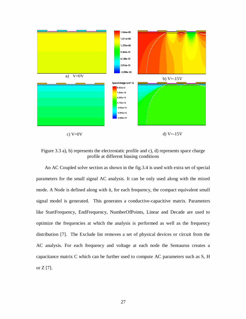
27
a) V=0V
b) V=-15V
c) V=0V
d) V=-15V
Figure 3.3 a), b) represents the electrostatic profile and c), d) represents space charge
profile at different biasing conditions
An AC Coupled solve section as shown in the fig.3.4 is used with extra set of special
parameters for the small signal AC analysis. It can be only used along with the mixed
mode. A Node is defined along with it, for each frequency, the compact equivalent small
signal model is generated. This generates a conductive-capacitive matrix. Parameters
like StartFrequency, EndFrequency, NumberOfPoints, Linear and Decade are used to
optimize the frequencies at which the analysis is performed as well as the frequency
distribution [7]. The Exclude list removes a set of physical devices or circuit from the
AC analysis. For each frequency and voltage at each node the Sentaurus creates a
capacitance matrix C which can be further used to compute AC parameters such as S, H
or Z [7].

28
Figure 3.4 AC Analysis using Sentaurus
ON capacitance is calculated using the formulae as shown below,
= 2.7561e-12 F
Where Cb and Cd are the barrier and dielectric capacitance which are calculated using
permittivity of the free space (ε0) and the dielectric permittivity of the barrier and
dielectric. OFF capacitance was measured to be as
COFF1 = 0.15e-12 F
These results of analytical formulas were compared with simulated CV dependencies.
Fig3.5 represents the Sentaurus simulated CV plots during varying biasing conditions.

29
Figure 3.5 CV plot simulated using Sentaurus with varying bias condition
Sentaurus creates the capacitance matrix C from which the capacitance under the MIS
electrode were considered for comparison with analytical values. The device ON and
OFF capacitances of three terminal MIS varactor are determined from the simulated CV
plot as follows.
CON = 2.2e-12 F and COFF = 1.16e-13 F
From earlier research works, capacitance estimated for two terminal C3 varactor by
using analytical formulas is
CON = 2.7561e-12 F and COFF = 0.15e-12 F

30
The simulated results of three terminal MIS varactor are compared with the
analytical results of the two terminal C3 varactor. The expected result of this comparison
is that the ON-capacitance is close to the approximation described above (series
connection of two capacitors) but the OFF capacitance is not exactly equal to simplified
analytical expressions. Sentaurus simulated three terminal MIS varactor OFF capacitance
is much lower than the experimentally measured two terminal OFF capacitance. This
increases the Isolation. This low OFF capacitance is possible in three terminal MIS
varactor because both the MIS electrodes are depleted simultaneously in the OFF state
which leads to very low capacitance whereas in two terminal C3 varactor out of the two
electrodes only turns OFF and the other remains ON (only one electrode is depleted and
the other is accumulated). Hence the series capacitance of the two electrodes remains
high which leads to higher OFF capacitance values when compared to three MIS
varactor.
3.2. Effect of defects in AlGaN/GaN heterostructure on varactor C-V characteristics
AlGaN/GaN heterostructures typically have very high defect concentration in the
GaN buffer layer. Typical measured acceptor trap concentration is approximately 1e16
cm^-3 and its energy level varies from 0.3eV to 0.5eV from conduction band [8]. This is
due to the fact that these heterostructures are grown over SiC or sapphire or Si substrates,
which have the lattice constant different from that of GaN. Therefore, the defect
generation during the material growth and device processing is nearly inevitable. In GaN
HEMTs carrier trapping by the defects is a major issue which severely limits the
performance of high-speed amplifiers and power switches [8]. Current collapse is a trap
related phenomenon limiting the output power which affects the device switching

31
response (a critical parameter for satellite communication). This current collapse occurs
when the hot carriers are injected and trapped outside the conduction band in the GaN
buffer layer. Current flowing through the transistor channel is directly affected by the
traps, which in turn affects the switching range, insertion loss, isolation loss and
switching time [9].
MIS varactor device uses CV dependence to achieve switching as opposed to I-Vs
used in HEMT device for the same purpose. The C-V dependence is expected to be
affected by traps much weaker than the I-V. Indeed, when certain amount of electrons in
the 2DEG channel is trapped by the defects, the HEMT current decreases proportionally,
which directly affects the gain, transconductance, insertion loss and other characteristics
of the HEMT based circuits. However, the same amount of trapped carriers will not have
significant effect on the C-V characteristics as long as the 2DEG still exists. We therefore
expect the varactor performance to be much less vulnerable to the defects than that of
HEMT.
In the presence of defects, analytically obtaining accurate electric field, electron
density, space charge and other profiles in the MIS varactor is nearly impossible. We
therefore have carried out the simulation of these profiles along with C-Vs of varactor in
presence of defects using Synopsys Sentaurus simulations.
In the considered modeling experiments, acceptor bulk traps are used which are
distributed uniformly across the GaN buffer layer. In Sentaurus, the traps are modeled
with Shockley-Read-Hall recombination in the continuity equation. Acceptor trap in GaN
buffer layer with different energy level from 0.3 eV to 0.5eV below the conduction band

32
were used for experiments. Varying concentration from 1e16 cm-3
to 1e18 cm-3
were used
for each energy level to study about the behavior of traps and its effects. Cross section of
1e-15 cm2 were used for the electron and hole capture cross sections which is consistent
with other reported numerical simulation. In Fig. 3.6 the CV plots depicts effect of traps
on the capacitance.
Figure 3.6 (a) CV dependencies of MIS varactor without traps (same as in Figure 3.5 -
shown here for comparison)

33
(b) CV dependencies with acceptor trap concentration 1016
cm-3
.
(c) CV dependencies with acceptor trap concentration 1018
cm-3
; this plot corresponds to
a very high defect concentration, normally not present in a decent quality
heterostructures.

34
Peak capacitance or the ON capacitance values are nearly not affected by traps
whereas the OFF capacitance is marginally affected by the traps. Actual effect of the
traps is prominent in the eDensity profile of the device with increase in the negative bias
applied to the electrodes.
For further study of traps different types of traps with various concentrations were
used in simulation. Fig. 3.7 depicts effect of traps on the eDensity profile {a) & b)} MIS
varactor (without traps): bias applied from 0V to -15V on the MIS electrode. {c) & d)}
with acceptor traps with same biasing conditions as without traps. {e) & f)} with donor
traps with same biasing conditions as without traps.
a) V=0V
b) V=15V
c) V= 0V
d) V= -15V
e) V= 0V
f) V= -15V
Figure 3.7{a) & b)} eDensity profile of MIS Varactor (without traps): bias applied from
0V to -15V {c) & d)} acceptor traps with same biasing conditions {e) & f)} with donor
traps

35
Electrons in 2DEG channel are trapped by acceptor traps in GaN buffer layer and it is
clearly observable in the eDensity profile with the varying applied bias. In transistors,
changes in charge profile of 2DEG due to traps have a direct effect on the current
parameter which in turn affects the switching response. MIS varactor acts as a capacitor
and the capacitance value is not drastically affected when there are changes in electron
density of 2DEG which is the bottom plate of the capacitor. Capacitance values have
drastic changes only when the 2DEG disappears completely. To deplete the entire 2DEG
at zero bias a huge concentration of traps are required which is typically not possible. So
the capacitance profiles are less sensitive to the GaN buffer traps and hence switching
response in MIS varactor is better than regular transistors.
2.5 Comparison between the Three-terminal and two-terminal varactor RF switch
performance
RF performance characteristics of MIS varactor are simulated using MATLAB.
Device parameters such as sheet resistance, electrode spacing and length, width, ON state
and OFF state capacitance values are extracted from the Sentaurus simulation to use in
the MATLAB code.
In order to provide a matched simulation results a comparison of performance
parameters between the proposed three-terminal MIS varactor and studied and published
earlier two-terminal C3 device is presented. A MIS varactor device was simulated in the
Sentaurus software with device parameters exactly same as a C3 switch. Electrode length
and the spacing between them is 2um. An additional schottky electrode with 1 um length
is placed 1 um away from the MIS contacts. WSER and WSHT dimension set is chosen as
0.4mm/0.4 mm and sheet resistance as 310 ohm/sq. Negative bias voltage is applied to

36
MIS contacts to deplete the channel under them. Using Sentaurus CON was obtained as
2.2 pF/mm and COFF as 1.16e-13 F/mm. From the above design parameters we were able
to get isolation of 30dB at 18 GHz for the MIS varactor without any additional
compensating inductance added in the circuit whereas C3 was able to achieve only 25dB
at 18 GHz.
Figure 3.8 Insertion loss and isolation of the new three-terminal MIS varactor switch
compared with experimental and simulated of two-terminal varactor switch.
Device parameters of a regular MIS varactor device (simulated using Sentaurus) as
discussed earlier are used in MATLAB software to plot insertion loss and isolation.
Different sets of series and shunt device dimensions were used to find the best dimension
at fixed frequency 10 GHz.

37
Figure 3.9 Isolation and Insertion loss variation with increasing device width
Insertion loss and isolation is plotted for different voltage bias applied to the MIS
contacts. The turn off voltage is typically 6-9 V for MIS varactor [6]. Depending on the
voltage applied to MIS contacts the depletion region under them varies, this also alters
the electrode spacing length considered for capacitance calculation. In accordance with
the Sentaurus simulation, various COFF capacitance values at various voltages were used
in MATLAB simulation.
Figure 3.10 Isolation and Insertion loss with varying bias conditions

38
Trapping is the most damaging effect which limit the device performance and
reliability in GaN HEMTs. Various researches take place to study its behavior and lessen
its effect on devices. For comparative study, insertion and isolation loss are calculated
and plotted for various conditions such as MIS varactor device without any traps (ideal
case) and with different types of trap at different concentration.
Fig. 3.11 Insertion loss with variation in different type of traps
Fig. 3.12 Isolation with variation in different type of traps

39
To summarize, this chapter clearly explained CV and RF performance characteristics
of the new three terminal MIS varactor. Its results were compared with the experimental
results of the existing two terminal C3 varactor, where the Insertion loss is almost the
same but the Isolation of three terminal MIS varactor is lot better. This is clearly due to
the fact that the three terminal MIS varactor OFF capacitance is much lower than that of
the two terminal C3 varactor.

40
CHAPTER 4
TRANSIENT RESPONSE OF MIS VARACTOR
4.1 Transient response of C3 MIS varactor
Microwave switches are used in wide range of modern electronic systems including
communications systems, civilian and military radars, and electronic-warfare (EW)
systems. Microwave switches can be compared in terms of many different performance
parameters, although one of the clearest differentiators is switching speed. It is especially
important in applications that require the stacking of multiple switches in series. For the
communication between airplanes and satellites as well as for electrically steerable
antennas for radar systems, highly integrated RF-front-ends with good switching speed
are vital. This initiates the necessity to study the speed of response of microwave
switches.
A voltage-controlled capacitor (varactor) formed over 2DEG has been shown to have
high capacitance on/off ratio up to microwave frequencies, it was also suggested to be a
promising switching device [4]. Therefore it is important to study the expected speed of
response for MIS varactor switch to the applied bias.

41
In general transient response curves from which switching speed is depicted can be
defined as follows:
Switching speed is defined as the time needed to change the state of a switch port
from ON to OFF or from OFF to ON. Switching speed is often characterized in
two ways: Rise/Fall time, and ON/OFF time.
Rise time is the time it takes for the detected RF output to raise from 10% to 90%
of the final value, when a switch arm is changed from an OFF state to an ON
state.
Fall time is the time it takes for the detected RF output to drop from 90% to 10%
of the initial value, when a switch arm is changed from an ON state to an OFF
state.
Rise and fall times do not include the switch delay time.
ON time is the time period from 50% of the transition of the control signal to 90%
of the detected RF output when the switch arm is changed from an OFF state
(isolation) to an ON state (insertion loss).
OFF time is the time period from 50% of the transition of the control signal to
10% of the detected RF output when the switch arm is changed from an ON state
(insertion loss) to an OFF state (isolation).
The ON and OFF times include the switch propagation delay. Switching time of
an RF switch can be measured using an RF signal generator, a square law RF
detector (e.g. Schottky diode), a fast Rising/Falling edge (~10nsec) square wave
function (pulse) generator for switch control, and an oscilloscope

42
For a MIS Varactor which consists of two MIS contacts and a Schottky control
electrode all deposited over a planar AlGaN/GaN heterostructure which possess 2DEG
channel at the hetero interface. This varactor is said to be in ON state when there is zero
bias between the MIS electrodes, the varactor capacitance consists of two relatively large
capacitances between metal electrode and the 2DEG channel connected in series. At very
large negative bias voltage, the 2DEG is fully depleted and depletion region penetrates
deeply into the device where the capacitance drops to a very low value. This state is
termed as OFF state. Switching response of this varactor is studied using Sentaurus.
Representation of the MIS varactor structure is shown in the Fig 4.1.
Figure 4.1 2D MIS varactor structure
There are several factors that influence the response time of a varactor. The most
important is RC time constant. The ON-capacitance (CON) and the resistance (RON) of the

43
load form the RC time constant. The RC time constant is given by τRC = RON CON. When
the MIS varactor switch is turned ON or OFF, both the capacitance and resistance
changes. To estimate the upper limit of the RC time constant, maximum values are used
which corresponds to ohm state. While simulating MIS varactor, the measured ON-
capacitance (CON) is 2.26e-12 F which is the highest capacitance of the switch when
applied bias is equal to zero. Whereas the resistance (RON) is calculated with the other
parameters obtained from the simulation as shown below.
Length = (0.3 × LSCH) + (LGAP1) + (LMIS2) + (LGAP2) + (0.3 × LMIS2) = 3.6 μm; Width =
1mm
Length involved in calculating resistance during the ON state of the MIS varactor is
depicted in the Fig. 4.2.
Figure 4.2 Zoomed in figure of the device structure showing the length of metal contact
and electrode spacing

44
Resistance (RON) = 1.116 Ω where RON is the impedance of the transmission line
where the switch is connected or the load, RSH is sheet resistance is estimated as 310
Ω/sq, L is Length, W is Width.
τRC = RON × CON = 2.522-12
s
This τRC calculated using RON and CON is an intrinsic time constant value which is
theoretically achievable with this MIS varactor. In reality the MIS varactor electrodes are
connected to 50 Ohm transmission line as shown in the Fig. 4.3.
Figure 4.3 Circuit layout of MIS varactor switch
The time constant for this circuit which includes the transmission line with the MIS
varactor can be estimated as follows,
τRC = (RON + RTL ) × CON = (1.116 + 50) × 2.26e-12 = 115.522e-12 s
The capacitance of the varactor must be kept small to prevent the RC time constant
from limiting the response time. Trade-offs between fast transit times and low
45
capacitance are necessary for high-speed response. In the OFF state, the conduction
channel is depleted (pinched-off), which causes the MIS varactor to exhibit very high
resistance (RON), mechanism which provides good isolation at low frequencies. In reality
the actual switching speed might vary from ideal value because every switch has some
parasitic capacitance, inductance, resistance, and conductance. These parasitic
components combine to degrade the speed of response of the switch. To verify the
estimated RC time constant value of the MIS varactor, transient simulations were carried
out using the Sentaurus software.
For the Sentaurus simulations, study of transient response measured the internal time
constant of the device without any involvement of the external circuit. This enabled the
actual semiconductor device to be simulated instead of mixed mode. Sentaurus Device
computes the transient response of the MIS varactor to a voltage signal. Duration of the
input pulse is specified according to which the physical device equations are solved
consistently. A transient simulation is performed for the time duration specified in the
“Transient” command. In that command, the start time, final time, and step size
constraints (initial, maximum, minimum) are in seconds. Actual step sizes are determined
internally, based on the rate of convergence of the solution at the previous step.
“Increment” command determines the maximum step size increase [7]. Simulation results
are plotted automatically using the Inspect and it consists of transient response of the
output voltage, total current under MIS electrode through the n-channel with overlaying
the input pulse. “Time” command is used in the simulation to print the time in the
transient response plot [7]. For the MIS varactor time dependent boundary conditions are
46
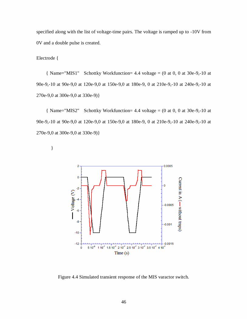
specified along with the list of voltage-time pairs. The voltage is ramped up to -10V from
0V and a double pulse is created.
Electrode {
{ Name="MIS1" Schottky Workfunction= 4.4 voltage = (0 at 0, 0 at 30e-9,-10 at
90e-9,-10 at 90e-9,0 at 120e-9,0 at 150e-9,0 at 180e-9, 0 at 210e-9,-10 at 240e-9,-10 at
270e-9,0 at 300e-9,0 at 330e-9)}
{ Name="MIS2" Schottky Workfunction= 4.4 voltage = (0 at 0, 0 at 30e-9,-10 at
90e-9,-10 at 90e-9,0 at 120e-9,0 at 150e-9,0 at 180e-9, 0 at 210e-9,-10 at 240e-9,-10 at
270e-9,0 at 300e-9,0 at 330e-9)}
}
Figure 4.4 Simulated transient response of the MIS varactor switch.

47
Simulation of transient response in Sentaurus had issues in charactering the speed of
switching because varactor does not have any current flowing through the channel. One
of the approach is to monitoring capacitance as a function of time during transient.
However this complicates the simulation because it requires AC signal and the pulse
signal to be applied at the same time which results in convergence issues. As an
alternative approach, current flowing through the gate is traced. In steady state this
current is zero and whenever this current is not zero there exists a transient. Transient plot
of MIS varactor is exactly like biased RC circuit. The current is zero before the ramp
starts and also zero after the ramping is over. DC current does not flow through the
capacitor. During the ramping, there is a current through capacitor according to i =
C*dV/dt. So the square wave response is observed. The total current curve does not
resemble the exact shape of the square waveform because in real device, on top of this
theoretical response there is a component related to internal charging-discharging of
varactor components.
4.2. Transient response in presence of defects
In hetero-structures, a junction formed with two different materials of different lattice
constant suffers inherent stress which leads to the formation of point defects and
threading dislocations which appear as traps. In the semiconductors, traps act like
“trapping center” for mobile charges in the region of defects. Effect of traps and self-
heating on the current transient response and the contribution of each factor is crucial for
the optimization of the performance of AlGaN/GaN HEMTs [8]. Studies that include
both effects in the current transient response simulation are still lacking. Generally in
HEMTs, the switching speed is strongly influenced by the traps that are present in the

48
bulk and the surface trapping mechanisms. A donor type trap is positively charged
(ionized) when empty and neutral when filled with an electron. An acceptor type trap is
neutral when empty and negatively charged (ionized) when filled with an electron. In
general the GaN bulk is filled with acceptor traps [8]. Electrons in the channel tunnel into
neighboring interface or they are injected into the buffer and get trapped in it by deep
level traps very quickly. Trapping of electrons lowers its energy. There is a preferable
path for electron going from higher energy to lower energy. Retrieving these trapped
electrons to conduction band is in slower process because the probability of escaping
from deep traps levels is relatively low. Depending upon the type of trap, level and
concentration of traps the escaping time varies from millisecond to seconds. This is the
main reason to simulate the transient response plots in the presence of deep traps in the
GaN buffer layer. For the study of trap behavior, different type of traps along with
various concentrations and positions of traps were simulated. Fig. 4.5 shows the
measured transient response of the MIS varactor switch with and without traps. For this
plot, acceptor traps are used in GaN buffer layer. Its concentration is 1e16 cm^-3 and its
position is 0.3eV form the Conduction Band.

49
Figure 4.5 Simulated transient response (with and without traps)
The response in the transient plots for the MIS varactor with the presence of the traps
is nearly the same as in ideal device without any defects. The reason for that is that, the
defects in GaN materials have very high activation energy and therefore it takes
significant time for those defects to charge - discharge. This time is typically in ms -
second range and is therefore much longer than the typical turn on - turn off times.
Therefore, during the transient, the charge state of defects does not change and their
effect on transient is minimal. This makes the varactor a really fast device.
Actual effect of the traps is prominent in the eDensity profile of the device with
increase in the negative bias applied to the electrodes. The snapshots of the eDensity
profile at various time during the entire transient simulation is shown in the Fig. 4.6.

50
a) V=0V
e) V=0V
b) V= -3V
f) V= -3V
c) V= -7V
g) V= -7V
d) V= -10V
h) V= -10V
Figure 4.6 eDensity profile of MIS Varactor (with &without traps) during transient
response with varying bias conditions
In the above Fig. 4.6, images (a) to (d) represent the snapshots of eDensity profile of
MIS varactor without any traps added to it with increasing negative bias (from 0V to -
10V) applied to the control electrode. Whereas images from (e) to (h) represent the
eDensity profile with acceptor traps added to the GaN buffer layer at similar biasing
conditions as that of without traps. This clearly depicts the depletion of 2DEG with
increasing negative bias.
The experimentally measured switching characteristic of the varactor switch is shown
in Fig.4.7. The measurements were done on wafer using the probe station. The pulsed

51
control voltage was generated using HP 8011A pulse generator and switching response
was observed using a Tektronix TDS 2022C oscilloscope [6]. The signal from the pulse
generator biased the varactors via the coaxial cable connected to the probes. The RF
signal was applied at 2 GHz frequency and the signal amplitude was 0 dBm. The pulsed
voltage amplitude was applied in the range from 10-15V. The limitations imposed by the
cable capacitances limited the achievable rise/fall time to around 0.8 – 0.9 μs [6]. As seen
from Fig 4.7, the varactors do not add any delay to the input pulses
Figure 4.7 Switching time of Schottky C3 varactor Switch; yellow line-applied pulsed
control voltage; blue line-Turn ON (fall time) and Turn OFF (rise time) times
The estimates show that varactor based switch response time is well below 0.1 μs [6].
The on-wafer measurements would not allow to resolve the nanosecond or sub
nanosecond rise/fall time due to parasitic parameters of probes and connecting cables. In
the future work it would be interesting and important to characterize the switching time
of varactor using RF packages with minimized parasitic parameters.

52
CHAPTER 5
CONCLUSION
In this work, we studied a novel type of RF switch based on III-Nitride varactor.
Unlike HEMTs, varactor uses capacitance modulation to control the flow of RF signal
and offers a number of advantages over HEMTs: they allow for shorter channel, do not
have gates or ohmic contacts and hence the fabrication is alignment- and anneal - free,
they do not consume DC current and provide the DC block. Unlike regular varactor
diodes, in this work, we analyze three-terminal varactor having independent control
electrode which further enhances the switch performance.
RF switch analysis of the MIS varactor is done by modeling and simulation using
Synopsys Sentaurus tools and MATLAB. CV characterizations were performed and the
obtained results are compared with available experimental data of two terminal C3
varactor. We were able to get isolation of 30dB at 18 GHz for the MIS varactor whereas
C3 was able to achieve only 25dB at 18 GHz. This is possible because the Sentaurus
simulated three terminal MIS varactor OFF capacitance is much lower than the
experimentally measured two terminal OFF capacitance. This low OFF capacitance is
possible in three terminal MIS varactor because both the MIS electrodes are depleted
simultaneously in the OFF state which leads to very low capacitance whereas in two
terminal C3 varactor out of the two electrodes only turns OFF and the other remains ON
(only one electrode is depleted and the other is accumulated). Hence the series

53
capacitance of the two electrodes remains high which leads to higher OFF capacitance
values when compared to three MIS varactor.
Modeling approach allows obtaining device characteristics and material dependencies
that are hardly achievable in experiments, such as effect of donor and acceptor traps.
Acceptor traps were simulated in the GaN buffer layer and its effect on the switch
performance characteristics were studied. Peak capacitance or the ON capacitance values
are nearly not affected by traps whereas the OFF capacitance is marginally affected by
the traps. MIS varactor device uses CV dependence to achieve switching as opposed to I-
Vs used in HEMT device for the same purpose. The C-V dependence is expected to be
affected by traps much weaker than the I-V. Therefore the varactor performance is less
vulnerable to the defects than that of HEMT.
Transient response is demonstrated with nanosecond response where results were in
agreement with the theoretical prediction. The response in the transient plots for the MIS
varactor demonstrated good stability with the presence of the traps. The reason for that is
that, the defects in GaN materials have very high activation energy and therefore it takes
significant time for those defects to charge - discharge. This time is typically in ms -
second range and is therefore much longer than the typical turn on - turn off times. This
makes the varactor a really fast device. In overall the proposed three terminal MIS
varactor promises significant performance improvements over the existing two terminal
C3 device. In the future work it would be interesting and important to fabricate and
characterize the varactor device using RF packages with minimized parasitic parameters.

54
REFERENCES
[1] Khan, Muhammad Bilal. Third order nonlinearity in III-nitride microwave switches.
Diss. UNIVERSITY OF SOUTH CAROLINA, 2011.
[2] Simin, G., et al. "Novel approaches to microwave switching devices using nitride
technology." International Journal of High Speed Electronics and Systems 20.01 (2011):
219-227.
[3] Wang, Jingbo. High-performance gateless III-nitride microwave switches. Diss.
University of South Carolina, 2010.
[4] Jahan, Faisal. "High Performance RF Control Devices Using Capacitively Coupled
Contacts (C3) Over III-N Heterostructures." (2013).
[5] YANG, YI-HSUAN. "Electromagnetic Modeling of GaN Varactor Microwave
Switches." (2013).
[6] Gaevski, Mikhail, et al. "GaN microwave varactors with insulated
electrodes." physica status solidi (c) 11.3‐4 (2014): 853-856.
[7] Guide, Sentaurus Device User. "Version H-2013.03." Synopsys, Mountain View, CA,
USA (2013).
[8] Miccoli, Cristina, et al. "Trapping and thermal effects analysis for AlGaN/GaN
HEMTs by means of TCAD simulations." IEEE Electron Device Letters 34.9 (2013):
1121-1123.
[9] Charbonniaud, C., et al. "Electrothermal and trapping effects characterisation of
AlGaN/GaN HEMTs." (2003).