Embed Size (px)
Citation preview

Design of Hybrid SiC Varactor Driver Circuit
using SiC MESFET
Master of Science Thesis in Master Degree Program Wireless and
Photonics Engineering
IMRAN KHAN Microwave Electronics Laboratory Department of Microtechnology and Nanoscience - MC2 CHALMERS UNIVERSITY OF TECHNOLOGY Gothenburg, Sweden, 2012

i
Master Thesis
Design of Hybrid SiC Varactor Driver Circuit using SiC MESFET
IMRAN KHAN
Examiner Hans Hjelmgren
Microwave Electronics Laboratory Department of Microtechnology and Nanoscience CHALMERS UNIVERSITY OF TECHNOLOGY
Göteborg, Sweden, 2012
ii
Design of Hybrid SiC Varactor Driver Circuit using SiC MESFET
Imran Khan
© Imran Khan, 2012.
Technical Report No. Microwave Electronics Laboratory Department of Microtechnology and Nanoscience - MC2 Chalmers University of Technology SE-412 96 Göteborg Sweden Phone: +46 (0) 31 772 1000

iii
Design of Hybrid SiC varactor Driver Circuit using SiC MESFET Imran Khan Deparment of microtechnology and nanoscience MC2 Chalmers University of Technology Abstract The main challenge for mobile service providers is the exponential growth of the wireless data traffic and the increasing number of users. This challenge increases the complexity of radio base stations and power amplifiers. A lot of effort is done to increase the power amplifier efficiency, and dynamic load modulation is one of the successful techniques. A tunable matching network is used at the output to provide the optimum load for a specific output power. A varactor, voltage controlled capacitor, is used for the fast tuning of the matching network. In this thesis work a hybrid varactor driver circuit is designed and implemented to drive anti-series high power SiC Schottky varactors. These high power SiC varactors can provide a very high tuning ratio of 6:1 at a voltage swing of 60 V. Two types of varactor driver circuit configurations are simulated, implemented and compared in terms of important figure of merits like driver DC power consumption, driver bandwidth, anti-series varactor RF impedance, and driver linear static transfer function. In one configuration a high resistor is used for biasing the switching transistor and in the other configuration a gate to source connected MESFET is used for biasing the switching transistor. The designed driver circuit has average DC power consumption less than 1 W, isolation of driver and anti-series varactors less than -18 dB, driver speed above 3 MHz and driver output voltage from 2 to 50 V. The driver circuit configuration with two SiC MESFETs is faster (≥ 10 MHz), but it has a steeper static transfer function as compared to the configuration with one SiC MESFET and a high resistor.
Keywords: Hybrid Varactor driver circuit, SiC MESFET, SiC Varactor, Transient analysis, Advanced Design System (ADS) simulation, MMIC.

iv
Table of Contents Introduction ...................................................................................................................................... 1
1.1 SiC MESFET ..................................................................................................................... 2
1.2 SiC Varactor ......................................................................................................................... 3
Devices characterization .................................................................................................................. 5
2.1 SiC MESFET ........................................................................................................................ 5
2.1.1 IV Measurement ............................................................................................................. 5
2.1.2 S-Parameter measurement ............................................................................................. 7
2.1.3 Advanced Design System Model ................................................................................... 9
2.2 SiC Varactor ....................................................................................................................... 10
2.2.1 CV measurements ........................................................................................................ 10
2.2.2 Advanced Design System Model ................................................................................. 10
Varactor Driver Circuit Pre-Analysis ............................................................................................. 12
3.1 Varactor Driver Circuit Topology 1 ................................................................................... 12
3.1.1 Biasing Resistor (Rin) ..................................................................................................... 13
3.1.2 SiC MESFET Q2 .......................................................................................................... 14
3.1.3 Feed Network ................................................................................................................. 14
3.1.4 Anti-series Varactors...................................................................................................... 15
3.2 Varactor Driver Circuit Topology 2 ................................................................................... 15
3.2 Transient Analysis in MATLAB and ADS .......................................................................... 15
Hybrid Varactor Driver Circuit Design .......................................................................................... 18
4.1 Feed Network Design ......................................................................................................... 18
4.2 Varactor Driver Circuit Simulation .................................................................................... 24
4.3 Varactor Driver Circuit Results .......................................................................................... 26
4.3.1 Driver Results of Topology 1 ........................................................................................ 27
4.3.2 Driver Results of Topology 2 ........................................................................................ 30
4.4 Varactor Driver Layout ...................................................................................................... 34
4.5 Realistic Control Signal Measurement ............................................................................... 36
Conclusions and future work .......................................................................................................... 42
Acknowledgements ........................................................................................................................ 43
References ...................................................................................................................................... 44

v
Notations
Abbreviation
3G 3rd Generation mobile communication ADS Advanced Design System C-V Capacitance versus Voltage DC Direct Current DLM Dynamic Load Modulation LTE Long Term Evolution MESFET Metal Semiconductor Field Effect Transistor MMIC Monolithic Microwave Integrated Circuits PA Power Amplifiers RF Radio Frequency SiC Silicon Carbide
Designations
Vds Drain to source voltage V Vgs Gate to source voltage V Ids Drain current A gds Output conductance mS gm_max maximum transconductance mS Vpinch Pinch off voltage V Isat Saturated drain current A Rds Output resistance Ω Cv Varactor capacitance pF Cmax Varactor maximum capacitance pF Cmin Varactor minimum capacitance pF Lf Feed network inductor nH Cf Feed network capacitor pF Rf Feed network resistor Ω PDC Driver DC power consumption W Vdd Driver circuit bias voltage V Vd Driver output or varactor bias voltage V C Bias supply decoupling capacitor pF IQ1 Current through transistor Q1 A IQ2 Current through transistor Q2 A PDC_Q1 DC power consumption through transistor Q1 W PDC_Q2 DC power consumption through transistor Q2 W PDC_ave Average DC power consumption of varactor driver
circuit W

1
Chapter 1
Introduction In modern communication signals (3G, LTE and beyond) the power amplifier operates in back off state most of the time. For efficiency enhancement Dynamic Load Modulation (DLM) is used. It changes dynamically the output matching network of a Power Amplifier (PA) according to the incoming communication signal. The varactors based DLM is a fast technique that uses the varactors to dynamically change the load matching network of the PA. The varactor capacitance is controlled by a bias voltage. Figure 1 describes this principle of DLM.
Figure 1 DLM Transmitter Architecture [1]
Developing tunable matching network is important for DLM efficiency enhancement of PAs. The advantage of using varactor based tunable matching network is that it can tune very fast. An early work has been done to design the varactor based tunable matching network for DLM application [3]. The Micrometrics varactors that have a high tuning range with more than 80 V breakdown voltage were used in this work, but for biasing the varactors up to 80 V they used an external variable high voltage DC supply. In order to facilitate the biasing we need some DC to DC up convertor that can provide 60 V or even 80 V.
In this thesis work a DC to DC convertor or more specifically a driver circuit for varactors is developed. It takes a small voltage swing at the input and provides a high voltage swing of 60 V at the output for biasing the varactors. This high voltage swing will utilize the full tuning range of the varactors (Cmax to Cmin) to tune the load matching network instantaneously for optimum impedance. A hybrid driver circuit for varactors is designed, fabricated and measured by using SiC varactor, SiC MESFETs and some passive elements. This will be used as a base for a future

2
integrated (SiC varactor and SiC MESFET) driver circuit implementation in an advanced SiC MMIC process. By using the same material (SiC) for both devices (SiC varactor and SiC MESFET), they can be integrated on the same MMIC chip. Two types of driver circuit configurations are presented in this work. In one configuration a high-value resistor is used for biasing the SiC MESFET switching transistor, and in the other a gate to source connected SiC MESFET (current source) is used for biasing the switching transistor. Both configurations will be explained in detail in the driver topology sections.
This thesis work is divided into five chapters. In chapter 1 an introduction to the varactor driver circuit, SiC MESFET, SiC varactor and some previous work in this field is discussed. In chapter 2 device characterizations of SiC MESFET and SiC varactor devices together with their models are explained. Chapter 3 explains the varactor driver circuit topology 1 and 2 together with some transient analysis to select the transistors size. Chapter 4 focuses on the hybrid varactor driver circuit design; feed network design, varactor driver circuit simulation and results for topology 1 and 2, varactor driver layout, and realistic control signal measurements. Finally, the comparison of varactor driver circuit topology 1 and 2, conclusion and future work will be explained in chapter 5.
1.1 SiC MESFET
The SiC MESFETs [4] are high frequency power transistors fabricated in Chalmers clean room. The SiC material has high band gap, high electron saturation velocity and good thermal conductivity, which make these transistors suitable for high power and high frequency applications. This transistor is used in the driver circuit at a very low frequency (≤ 3 MHz), but it can sustain a very high voltage across drain to source (more than 100 volts) which makes it possible to get a high output voltage from the driver to the anti-series varactors.
Figure 2 shows the cross section of a standard SiC MESFET. It consists of a semi-insulating 4H-SiC substrate, a p buffer layer, an n channel layer, a high n doped cap layer, Ni ohmic contacts for source and drain, Ti/Pt/Au stack for Schottky gate, buried gate type structure and thermal oxide layer. The detail description about this type of device can be found in [4].

3
Figure 2 Schematic of standard SiC MESFET structure [4].
1.2 SiC Varactor The SiC varactor [5] is a Schottky diode that operates in the reverse bias condition and
behaves as a voltage controlled variable capacitor. The Schottky diode is a metal to semiconductor diode that has only one type of carriers (electrons), which makes it faster than the p-n junction diode. These SiC varactors are fabricated in Chalmers and developed for DLM applications. The typical specification of one of the available sizes of SiC varactors is given in Table 1 and figure 3 shows its C-V characteristics.
In order to get the full tuning range of these varactors from Cmin to Cmax (2.5 to 16 pF) a high voltage range (0 to 60 V) is required as shown in figure 3. The varactor driver circuit designed in this thesis work will provide this high voltage range to the varactors (at driver output) by using a small voltage range at the input of the varactor driver circuit.

4
Figure 3 CV plot of SiC Varactor [5].
Table 1 SiC varactor size and specification.
Parameters Values
Frequency 2 GHz
Size 7 Fingers Length 400 µm
Width 5 µm Width of Ohmic contacts 5-7 µm
Minimum capacitance Cmin 3 pF Maximum capacitance Cmax 16-18 pF
Vbias 0-60V
-60 -50 -40 -30 -20 -10 02
4
6
8
10
12
14
16
Bias voltage Vd [V]
Cap
acita
nce
Cv
[pF]

5
Chapter 2
Devices characterization
2.1 SiC MESFET Based on measurements on different SiC MESFET sizes, batch 4 devices were selected due to their low gate to source pinch-off voltage (typically 12 V). The measured results and developed Advanced Design System (ADS) models of two different sizes of transistors, 0.4×400 µm2 and 0.4×1000 µm2, will be provided in the following section. For the sake of simplicity the SiC MESFET of size 0.4 × 400 µm2 is denoted by symbol Q1 and 0.4 × 1000 µm2 by symbol Q2.
2.1.1 IV Measurement IV measurement values are extracted from the S-parameter measurement. Figure 4 and figure 5 show measured and simulated (ADS model) drain current (Ids) versus drain voltage (Vds) and drain current (Ids) versus gate voltage (Vgs) of a batch 4 device with the size of 0.4×1000 µm2
(Q2), respectively. The simulation results will be explained in the ADS model section below. This transistor has a maximum saturation current (Isat) of 280 mA at Vgs=0 V and a pinch of voltage (Vpinch) of -12 V as shown in figure 4 and figure 5, respectively. The breakdown is more than 100 V.
Figure 4 Drain current (Ids) vs. drain voltage (Vds) for different gate voltages (Vgs= -14 to 0 V) of a batch 4 device of size 0.4×1000 µm2. The plot indicates both the measured (red dots)
and simulation (blue lines) results.
0 5 10 15 20 25 30 35 40 45-50
0
50
100
150
200
250
300
Drain Voltage Vds [V]
Dra
in C
urre
nt I
ds [
mA
]
measuredsimulation
Vgs= -14V
Vgs= 0V

6
Figure 5 Drain current (Ids) vs. gate voltage (Vgs) for different drain voltages (Vds = 0 to 40 V) of a batch 4 device of size 0.4×1000 µm2. The plot indicates both the measured (red dots)
and simulation (blue lines) results.
Figure 6 and figure 7 show the IV measured and simulation (ADS model) results for a batch 4 device of size 0.2×400 µm2 (Q1). This device has the maximum saturation current of 115 mA and a pinch off voltage of -12 V with a breakdown voltage of more than 100V.
Figure 6 Drain current (Ids) vs. drain voltage (Vds) for different gate voltages (Vgs= -14 to 0 V) of a batch 4 device of size 0.4×400 µm2. The plot indicates both the measured (red dots) and
simulation (blue lines) results.
-20 -15 -10 -5 0 5-50
0
50
100
150
200
250
300
Gate Voltage Vgs [V]
Dra
in C
urre
nt I
ds [
mA]
measuredsimulation
Vds= -14V
Vds= 0V
0 5 10 15 20 25 30 35 40 45-20
0
20
40
60
80
100
120
Drain Voltage Vds [V]
Dra
in C
urre
nt I
ds [
mA
]
measuredsimulation
Vgs= 0V
Vgs= -14V

7
Figure 7 Drain current (Ids) vs. gate voltage (Vgs) for different drain voltages (Vds = 0 to 40 V) of batch 4 device of size 0.4×400 µm2. The plot indicates both the measured (red dots) and
simulation (blue lines) results.
2.1.2 S-Parameter measurement S-parameter measurement is carried out using Agilent network analyzer. Figure 8 and figure 9 show measured and simulation (ADS model) plots for gds vs. Vds for different Vgs values, for both device sizes. The most important device parameters extracted from measured S-parameters on both device sizes (0.4×1000 µm2 and 0.4×400 µm2) are listed in table 2.
Figure 8 Output conductance (gds) vs. drain voltage (Vds) for different gate voltages (Vgs= -14 to 0 V) of a batch 4 device of size 0.4×1000 µm2. The plot indicates both the measured (red
lines) and simulation (blue lines) results.
-30 -25 -20 -15 -10 -5 0 5-20
0
20
40
60
80
100
120
Gate Voltage Vgs [V]
Drai
n Cu
rrent
Ids
[mA]
measuredsimulation
Vgs=-14V
Vgs=0V
0 5 10 15 20 25 30 35 40-10
0
10
20
30
40
50
60
Vds [V]
gds [
mS]
Vgs=0V
Vgs= -14V
Measured = Red lines
Simulation = Blue lines

8
Figure 9 Output conductance (gds) vs. drain voltage (Vds) for different gate voltages (Vgs= -14 to 0 V) of a batch 4 device of size 0.4×400 µm2. The plot indicates both the measured
(red lines) and simulation (blue lines) results.
Table 2 List of important parameters of SiC MESFET for device sizes of 0.4×1000 µm2 and 0.4×400 µm2.
Parameters Q2 (0.4×1000 µm2) Q1 (0.4×400 µm2)
Maximum transconductance (gm_max) 35.34 mS 13.6 mS
Drain current at Vgs = 0V (Ids_sat) 273 mA (at Vds = 20 V)
100 mA (at Vds = 20 V)
Drain current at Vgs ≤ Vpinch (Ids_off) 10 mA (at Vds = 40 V)
9 mA (at Vds = 40 V)
Output conductance at Vgs = 0V (gds_on) 19 mS 51 mS
Output conductance at Vgs ≤ Vpinch (gds_off) 0.9 µS 0.27 µS
Drain to source capacitance (Cds) 0.27 pF 0.06 pF
Pinch off voltage (Vpinch) -12 V -12 V
0 5 10 15 20 25 30 35 400
2
4
6
8
10
12
14
16
18
20
Vds [V]
gds
[mS
]
Vgs = 0V
Vgs = -14 V
Measured = Red lines
Simulation = Blue lines

9
2.1.3 Advanced Design System Model In order to carry out the transient analysis and simulation of the driver circuit in ADS, transistor models are developed for both Q1 and Q2. These devices are modelled using symbolically defined devices two ports (SDD2P) featured in ADS. Figure 10 shows the schematic of the transistor model. Different variables are used for Q1 and Q2. In order to compare the accuracy of the transistor models the measured and simulation results (IV and gds plot) of the models are plot together in the same figure. Figure 4, 5, and 8 above show Ids vs. Vds, Ids vs. Vgs and gds vs. Vgs for Q2, while figure 6, 7, and 9 show the same characteristics for Q1.
Figure 10 Schematic of SiC MESFET model. Different variables are used for Q1 and Q2.
It can be seen by comparing the measured and simulation plots (IV and gds) in figures 4-9 that these models are just basic DC models that are developed specially for this project. Still though these DC models match the measured results fairly well and are good enough for the driver circuit transient simulation.

10
2.2 SiC Varactor The high power SiC varactor [5] fabricated in-house (Chalmers University) is used in this project work. A varactor with 7 fingers is used in measurement, ADS modelling, and transient simulation of the driver circuit.
2.2.1 CV measurements CV measurement of 7 finger size of SiC varactor is carried out. Figure 11 shows the capacitance vs. bias voltage for both measured and model simulation results of a SiC varactor with 7 fingers. This varactor has a tuning ratio of 1: 5.3, and an anti-series varactors is used basically to increase the power handling.
Figure 11 Measured and simulated capacitance (Cv) vs. bias voltage (Vd) of SiC varactor with 7 fingers.
2.2.2 Advanced Design System Model An advanced ADS nonlinear model of a SiC varactor that is already available in house Chalmers is used in this work. Figure 12 shows the ADS schematic of this nonlinear model. Details about this nonlinear model can be found in [6]. The model accuracy can be seen in figure 11 above that shows that the measured and simulation results are perfect inline for a varactor size of 7 fingers.
-60 -50 -40 -30 -20 -10 01
2
3
4
5
6
7
8
9
Bias voltage Vd [V]
Cap
acita
nce
Cv
[pF]
simulationmeasured

11
Figure 12 Schematic of SiC varactor nonlinear model [5].

12
Chapter 3
Varactor Driver Circuit Pre-Analysis
In this section two types of varactor driver circuit topologies, topology 1 and topology 2, are discussed and a transient analysis is carried out in order to select the suitable device size among many available sizes. The important figures of merit related to the varactor driver circuit are DC power consumption, driver bandwidth, anti-series varactors RF impedance, and driver linear static transfer function. These figures of merit will be explained in the relevant sections. Table 3 lists the requirements of the varactor driver circuit and DLM specific application values.
Table 3 Varactor driver and DLM specific application parameter values.
Parameters Values
RF Frequency 2 [GHz]
PA output peak power 100-120 [W]
Driver DC power consumption ≤ 1 [W]
Driver and anti-series varactors isolation ≤ -20 [dB]
Driver bandwidth (speed) DC – 10 [MHz]
Anti-series varactors RF impedance change Minimum
Varactor bias voltage 2-60 [V]
Driver static transfer function Linear
3.1 Varactor Driver Circuit Topology 1
The Varactor driver circuit topology 1 is shown in figure 13. It consists of four main parts, (1) Rin, (2) SiC MESFET, (3) Feed network, and (4) anti-series varactors. The circuit is described in a generalized form with given range of values depending on the application together with the specific component values that is used in this project work.

13
Q2
Rfeed(50Ω to 400Ω)
Lfeed(1nH to 30 nH)
RFin (1 to 3 GHz)
RFout (1 to 3 GHz)
Control signal at Vgs
(DC to 10 MHz)
Vdd (40 to 70 V)
Anti S
eries varactors
Cfeed (1pF to 20pF)
Rin (1kΩ to 3kΩ)
Vc (1 to 70 V
)
Feed network
Figure 13 Varactor driver circuit topology using high resistor (Rin)
3.1.1 Biasing Resistor (Rin)
A large resistor (1 kΩ to 3 kΩ) is used to bias the transistor and varactors via a feed network. Depending on the value of applied bias voltage (Vdd) the resistor Rin will define the drain current (Ids) flowing through the transistor Q2 and that in turns give the DC power consumption of the driver circuit. The Rin value together with the feed network component values will define the time constant or speed of the driver circuit. The speed of the driver means how fast the driver can fully charge and discharge the anti-series varactor. The driver speed and DC power consumption are inversely proportional. In this project work Rin = 1.8 kΩ is used which will give us PDC= 1 W and a maximum driver speed of 3 MHz. The results are shown in the driver simulation and measurement sections. ´

14
3.1.2 SiC MESFET Q2
The SiC MESFET (0.4×1000 µm2) is used as a control device (non-linear) that will control the bias voltage of the anti-series varactors (Vc) at the output according to the input control signal provided at the gate as shown in figure 13 above. By sweeping the control signal from Vgs ≤ Vpinch to Vgs = 0 V a sweep of Vc from Vcmin to Vdd can be achieved. The Vcmin (typ 1 to 4 V) is obtained from the voltage division of Rin and Rds (of Q2). Vc and Vgs are inversely proportional, and a DC sweep of Vc vs. Vgs will give us the driver static transfer function, which is required to be as linear as possible. These plots are provided in the driver simulation and measurement section. Figure 14 shows the IV plot of a SiC MESFET (0.4×1000 µm2) together with a typical load line. Due to the high value of Rin the load line is flatter, which will give us a very high voltage gain at the output (drain to source) due to the small input voltage at the gate with small drain current (Ids).
Figure 14 Drain current (Ids) vs. drain voltage (Vds) and load line.
3.1.3 Feed Network The feed network consists of inductor Lf and capacitor Cf together with a resistor Rf as shown in figure 13 above. Its function is to isolate the anti-series varactors from the driving transistors. This network will allow the DC or low frequency signal to pass from the transistor to the varactors and will block the RF signal leaking into the transistor. The passive component values of the feed network will modify the anti-series varactors RF impedance and also the speed of the driver circuit. The sweeps of Lf, Cf and Rf are performed and explained in the driver circuit simulation section and optimum values of 21 nH, 1 pF and 200 Ω are selected, respectively.
0 5 10 15 20 25 30 35 400
50
100
150
200
250
300
Drain Voltage Vds [V]
Dra
in C
urre
nt I
ds [
mA]
Vgs= 0V
Load Line
15
3.1.4 Anti-series Varactors To get the high power handling anti-series varactors are used. The RF signal flows through the anti-series varactors and the hybrid driver circuit will provide the high bias voltage (Vc) at the junction as shown in figure 13 above.
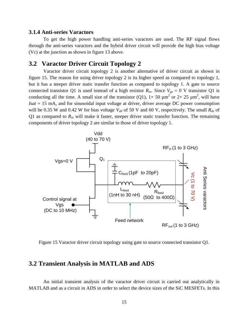
3.2 Varactor Driver Circuit Topology 2 Varactor driver circuit topology 2 is another alternative of driver circuit as shown in
figure 15. The reason for using driver topology 2 is its higher speed as compared to topology 1, but it has a steeper driver static transfer function as compared to topology 1. A gate to source connected transistor Q1 is used instead of a high resistor Rin. Since Vgs = 0 V transistor Q1 is conducting all the time. A small size of the transistor (Q1), 1× 50 µm2 or 2× 25 µm2, will have Isat = 15 mA, and for sinusoidal input voltage at driver, driver average DC power consumption will be 0.35 W and 0.42 W for bias voltage Vdd of 50 V and 60 V, respectively. The small Rds of Q1 as compared to Rin will make it faster, steeper driver static transfer function. The remaining components of driver topology 2 are similar to those of driver topology 1.
Q1Vgs=0 V
Rfeed(50Ω to 400Ω)
Lfeed(1nH to 30 nH)
RFin (1 to 3 GHz)
RFout (1 to 3 GHz)
Control signal at Vgs
(DC to 10 MHz)
Vdd (40 to 70 V)
Anti Series varactors
Cfeed (1pF to 20pF) Vc (1 to 70 V)
Feed network
Figure 15 Varactor driver circuit topology using gate to source connected transistor Q1.
3.2 Transient Analysis in MATLAB and ADS
An initial transient analysis of the varactor driver circuit is carried out analytically in MATLAB and as a circuit in ADS in order to select the device sizes of the SiC MESFETs. In this
16
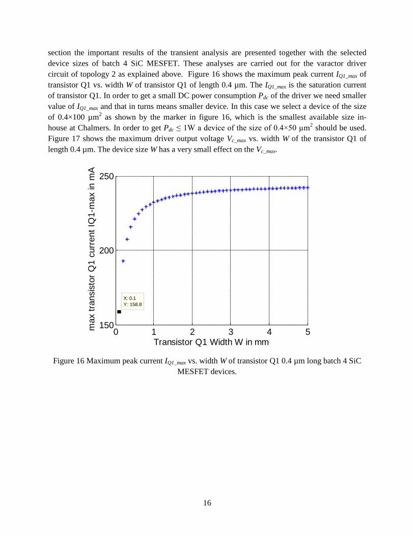
section the important results of the transient analysis are presented together with the selected device sizes of batch 4 SiC MESFET. These analyses are carried out for the varactor driver circuit of topology 2 as explained above. Figure 16 shows the maximum peak current IQ1_max of transistor Q1 vs. width W of transistor Q1 of length 0.4 µm. The IQ1_max is the saturation current of transistor Q1. In order to get a small DC power consumption Pdc of the driver we need smaller value of IQ1_max and that in turns means smaller device. In this case we select a device of the size of 0.4×100 µm2 as shown by the marker in figure 16, which is the smallest available size in-house at Chalmers. In order to get Pdc ≤ 1W a device of the size of 0.4×50 µm2 should be used. Figure 17 shows the maximum driver output voltage Vc_max vs. width W of the transistor Q1 of length 0.4 µm. The device size W has a very small effect on the Vc_max.
Figure 16 Maximum peak current IQ1_max vs. width W of transistor Q1 0.4 µm long batch 4 SiC MESFET devices.
0 1 2 3 4 5150
200
250
X: 0.1Y: 158.8
Transistor Q1 Width W in mm
max
tran
sist
or Q
1 cu
rren
t IQ
1-m
ax in
mA

17
Figure 17 Maximum driver output voltage Vc_max vs. width W of transistor Q1 0.4 µm long batch 4 SiC MESFET devices.
Figure 18 shows the minimum driver output voltage vs. width W of transistor Q2 of 0.4 µm long device. In order to achieve the lowest value of Vc_min we need as large device size as possible. The device of the size 0.4×1000 µm2 is selected as shown by the marker in figure 18.
Figure 18 Minimum driver output voltage Vc_min vs. width W of transistor Q2 0.4 µm long batch 4 SiC MESFET devices.
0 1 2 3 4 559.2
59.3
59.4
59.5
59.6
59.7
59.8
59.9
60
X: 0.1Y: 59.29
Transistor Q1 Width W in mm
max
driv
er o
utpu
t vol
tage
Vc-
max
in V
0 1 2 3 4 50
5
10
15
20
X: 1Y: 4.52
Width W in mm
Min
driv
er o
utpu
t vol
tage
Vc-
min
in V
18
Chapter 4
Hybrid Varactor Driver Circuit Design In this section the hybrid driver circuit design is explained. Transient simulation of driver circuit is carried out in ADS using the SiC MESFET and varactor models together with the passive components of the feed network. Both types of driver circuit topologies, topology 1 and 2 explained in section 3.1 and 3.2 above, are simulated and their results are compared in terms of important figure of merits. The varactor driver circuit implementation in MMIC will have some limitation, which is also explained together with varactor driver layout.
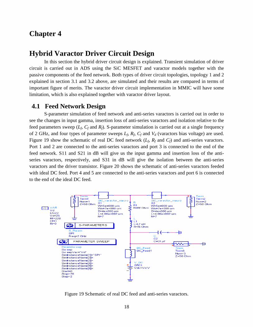
4.1 Feed Network Design S-parameter simulation of feed network and anti-series varactors is carried out in order to see the changes in input gamma, insertion loss of anti-series varactors and isolation relative to the feed parameters sweep (Lf, Cf and Rf). S-parameter simulation is carried out at a single frequency of 2 GHz, and four types of parameter sweeps Lf, Rf, Cf and Vd (varactors bias voltage) are used. Figure 19 show the schematic of real DC feed network (Lf, Rf and Cf) and anti-series varactors. Port 1 and 2 are connected to the anti-series varactors and port 3 is connected to the end of the feed network. S11 and S21 in dB will give us the input gamma and insertion loss of the anti-series varactors, respectively, and S31 in dB will give the isolation between the anti-series varactors and the driver transistor. Figure 20 shows the schematic of anti-series varactors feeded with ideal DC feed. Port 4 and 5 are connected to the anti-series varactors and port 6 is connected to the end of the ideal DC feed.
Figure 19 Schematic of real DC feed and anti-series varactors.

19
Figure 20 Schematic of ideal DC feed and anti-series varactors.
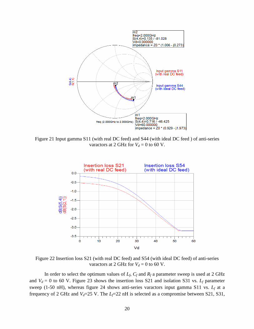
In order to see the changes in input gamma and insertion loss of anti-series varactors due to feed network, the input gamma S44 (with ideal DC feed), S11 (with real DC feed) and insertion loss S54 (with ideal DC feed), S21 (with real DC feed) are shown in figure 21 and figure 22, respectively. Optimum values of feed network parameters (Lf=22 nH, Cf=1 pF and Rf=220 Ω) are used. It can be noticed from the figures that S11 and S44 have a very small difference and the same applies for S21 and S54.
20
Figure 21 Input gamma S11 (with real DC feed) and S44 (with ideal DC feed ) of anti-series varactors at 2 GHz for Vd = 0 to 60 V.
Figure 22 Insertion loss S21 (with real DC feed) and S54 (with ideal DC feed) of anti-series varactors at 2 GHz for Vd = 0 to 60 V.
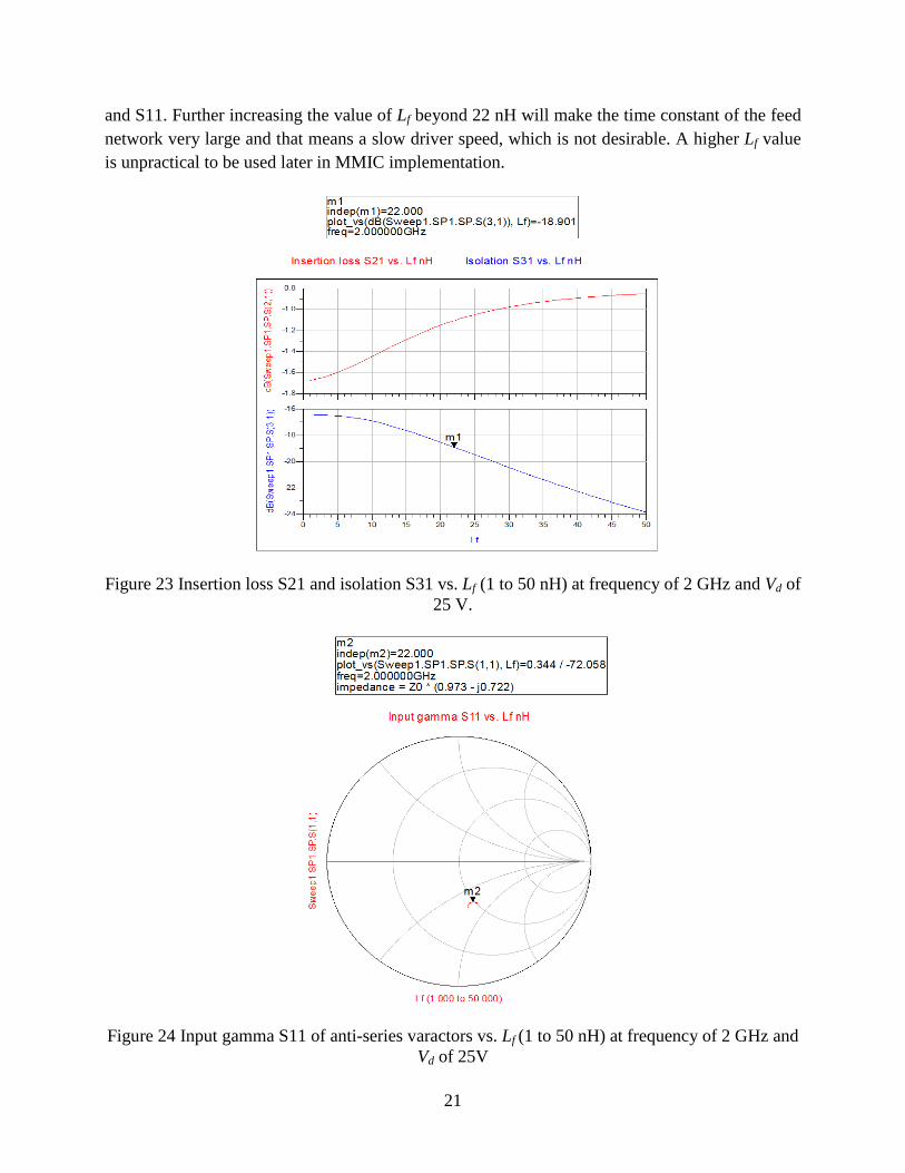
In order to select the optimum values of Lf, Cf and Rf a parameter sweep is used at 2 GHz and Vd = 0 to 60 V. Figure 23 shows the insertion loss S21 and isolation S31 vs. Lf parameter sweep (1-50 nH), whereas figure 24 shows anti-series varactors input gamma S11 vs. Lf at a frequency of 2 GHz and Vd=25 V. The Lf=22 nH is selected as a compromise between S21, S31,
21
and S11. Further increasing the value of Lf beyond 22 nH will make the time constant of the feed network very large and that means a slow driver speed, which is not desirable. A higher Lf value is unpractical to be used later in MMIC implementation.
Figure 23 Insertion loss S21 and isolation S31 vs. Lf (1 to 50 nH) at frequency of 2 GHz and Vd of 25 V.
Figure 24 Input gamma S11 of anti-series varactors vs. Lf (1 to 50 nH) at frequency of 2 GHz and Vd of 25V

22
Figure 25 shows the insertion loss S21 and isolation S31 vs. Cf parameter sweep (1-30 pF), and figure 26 shows anti-series varactors input gamma S11 vs. Cf at frequency of 2 GHz and Vd = 25 V. It can be noticed from the figures that Cf has a small effect on S21 and S11, but more effect on S31. The Cf= 1 pF values is selected because S31= -18.9 dB is enough for isolation and by increasing its value more than 1 pF will make the time constant of the feed network very large and that means a slow driver speed.
Figure 25 Insertion loss S21 and isolation S31 vs. Cf (1 to 30 pF) at frequency of 2 GHz and Vd of 25 V.

23
Figure 26 Input gamma S11of anti-series varactors vs. Cf (1 to 30 pF) at frequency of 2 GHz and Vd of 25 V
Finally, figure 27 shows the S21 and S31 vs. Rf parameter sweep (5-500 Ω), and figure 28 shows S11 vs. Rf at a frequency of 2 GHz and Vd = 25 V. Optimum value of Rf= 220 Ω is selected as a compromise between S21, S31and S11.
Figure 27 Insertion loss S21 and isolation S31 vs. Rf (5 to 500 Ω) at frequency of 2 GHz and Vd of 25 V.

24
Figure 28 Input gamma S11 of anti-series varactors vs. Rf (5 to 500 Ω) at a frequency of 2 GHz and Vd of 25V.
4.2 Varactor Driver Circuit Simulation Transient simulation of both driver circuit topology 1 and topology 2 are carried out in ADS. Figure 29 shows the ADS schematic of varactor driver circuit topology 1. A high value resistor Rin of 1.8 kΩ is used for biasing the transistor Q2 (ADS model). The Lf, Rf and, Cf together make the feed network. The driver output voltage Vc feeds two anti-series varactor (ADS models) and their opposite ends are terminated with two 50 Ω terminations to provide the ground for the opposite end of the varactors. Due to a maximum available DC supply of 50 V during measurement, a bias voltage Vdd= 50 V is used instead of 60 V to match the simulation and measured results.. A DC bias voltage Vdd = 50 V is applied to the drain of the transistor via Rin and a decoupling capacitor C=100 nF is used near DC supply voltage. A sinusoidal input voltage of DC level -8 V and amplitude of 7.3 V is applied at the input gate of the transistor. Transient simulation is carried out of the circuit and initial conditions are used for the reactive components.

25
Figure 29 Schematic of varactor driver circuit topology 1.
Figure 30 shows the schematic of the varactor driver circuit of topology 2. In this schematic Rin is replaced by a gate to source connected SiC MESFET Q1 that is used for biasing the circuit. Q1 will act like a current source that will provide the current to the circuit and due to its nonlinear Rds the overall driver static transfer function will be more nonlinear than topology 1. The remaining components of driver circuit topology 2 are connected in the same way as in driver circuit topology 1.

26
Figure 30 Schematic of varactor driver circuit topology 2.
4.3 Varactor Driver Circuit Results In this section the results of driver output voltage Vc vs. driver input voltage Vin for different frequencies, driver static transfer function, instantaneous current IQ1 (through Rin or Q1), IQ2 (through Q2), DC power consumption PDC, and average DC power consumptions PDC_ave are explained. In order to check the driver speed different frequency signals are applied at the input of the driver and driver output voltage Vc is observed. The driver output voltage Vc needs to reach the full swing between Vcmin (1 to 4 V) and Vdd in order to drive the varactor full tuning range.

27
4.3.1 Driver Results of Topology 1 Figures 31-33 show measured and simulated output voltage Vc together with driver input voltage Vin for frequencies of 50 kHz, 100 kHz and 1MHz, respectively. The difference between measured and simulated Vc is due to the transistor model. Simulated and measured gds of transistor Q2 do not perfectly match as explained in section 2.1.2. It can be observed from figure 33 that the driver output voltage Vc can reach maximum value of 46.7 V at a frequency of 1 MHz and this is the maximum speed of the varactor driver circuit.
Figure 31 Measured and simulated driver output voltage Vc together with driver input voltage Vin at a frequency of 50 kHz of driver circuit topology 1.
-15 -10 -5 0 5 10 150
10
20
30
40
50
Time t [usec]
Driv
er o
utpu
t vol
tage
Vc
[V]
X: -4.842Y: 47.65
-15 -10 -5 0 5 10 15-20
-15
-10
-5
0
Driv
er in
put v
olta
ge V
in [
V]
Vc-simVc-measVin-meas
28
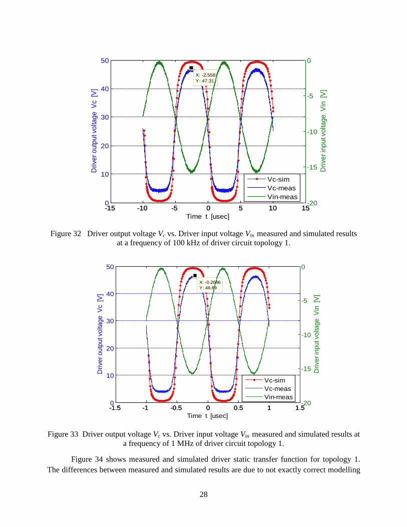
Figure 32 Driver output voltage Vc vs. Driver input voltage Vin measured and simulated results at a frequency of 100 kHz of driver circuit topology 1.
Figure 33 Driver output voltage Vc vs. Driver input voltage Vin measured and simulated results at a frequency of 1 MHz of driver circuit topology 1.
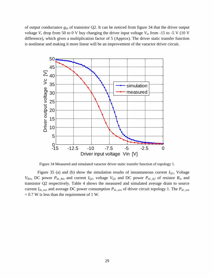
Figure 34 shows measured and simulated driver static transfer function for topology 1. The differences between measured and simulated results are due to not exactly correct modelling
-15 -10 -5 0 5 10 150
10
20
30
40
50
X: -2.558Y: 47.31
Time t [usec]
Driv
er o
utpu
t vol
tage
Vc
[V]
-15 -10 -5 0 5 10 15-20
-15
-10
-5
0
Driv
er in
put v
olta
ge V
in [
V]
Vc-simVc-measVin-meas
-1.5 -1 -0.5 0 0.5 1 1.50
10
20
30
40
50
Time t [usec]
Driv
er o
utpu
t vol
tage
Vc
[V]
X: -0.2046Y: 46.69
-1.5 -1 -0.5 0 0.5 1 1.5-20
-15
-10
-5
0
Driv
er in
put v
olta
ge V
in [
V]
Vc-simVc-measVin-meas
29
of output conductance gds of transistor Q2. It can be noticed from figure 34 that the driver output voltage Vc drop from 50 to 0 V buy changing the driver input voltage Vin from -15 to -5 V (10 V difference), which gives a multiplication factor of 5 (Approx). The driver static transfer function is nonlinear and making it more linear will be an improvement of the varactor driver circuit.
Figure 34 Measured and simulated varactor driver static transfer function of topology 1.
Figure 35 (a) and (b) show the simulation results of instantaneous current IQ1, Voltage VRin, DC power Pdc_Rin and current IQ2, voltage VQ2 and DC power Pdc_Q2 of resistor Rin and transistor Q2 respectively. Table 4 shows the measured and simulated average drain to source current Ids_ave and average DC power consumption Pdc_ave of driver circuit topology 1. The Pdc_ave = 0.7 W is less than the requirement of 1 W.
-15 -12.5 -10 -7.5 -5 -2.5 00
5
10
15
20
25
30
35
40
45
50
Driver input voltage Vin [V]
Driv
er o
utpu
t vol
tage
Vc
[V]
simulationmeasured

30
Figure 35 (a) Instantaneous current IQ1, voltage VRin and DC power Pdc_Rin of resistor Rin (b) Instantaneous Current IQ2, Voltage VQ2 and DC power Pdc_Q2 of transistor Q2. The frequency
of the input signal is 1 MHz.
Table 4 Simulation and measured average drain to source current Ids_ave and DC power consumption Pdc_ave at bias voltage Vd = 50 V of topology 1.
Parameters Simulation Results Measured results
Bias voltage Vd
50 V 50 V
Average drain to source current Ids_ave
13.5 mA 14 mA
Average DC power consumption Pdc_ave
0.67 W 0.7 W
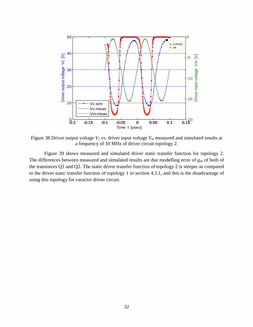
4.3.2 Driver Results of Topology 2 Figure 36-38 show the measured and simulated results of driver output voltage Vc vs. driver input voltage Vin at frequency of 1, 5, and 10 MHz, respectively. The differences between measured and simulated results are due to not exactly correct modeling of output conductance gds of both of the transistors Q1 and Q2. Figure 38 shows Vc and Vin at 10 MHz.Vc can reach 48 V at maximum and 8 V at minimum. The Vcmin= 8 V can be compensated by an offset at the varactors’ opposite ends instead of grounding. The driver results of topology 2 shows that it is faster and can reach a maximum driver speed of 10 MHz as compare to the driver results of topology 1 in section 4.3.1.

31
Figure 36 Measured and simulated driver output voltage Vc together with driver input voltage Vin at a frequency of 1 MHz of driver circuit topology 2.
Figure 37 Driver output voltage Vc vs. driver input voltage Vin measured and simulated results at a frequency of 5 MHz of driver circuit topology 2.
-1.5 -1 -0.5 0 0.5 1 1.50
10
20
30
40
50
Time t [usec]
Driv
er o
utpu
t vol
tage
Vc
[V]
X: -0.2409Y: 49.04
-1.5 -1 -0.5 0 0.5 1 1.5-20
-15
-10
-5
0
Driv
er in
put v
olta
ge V
in [
V]
Vc-simVc-measVin-meas
-0.2 -0.1 0 0.1 0.20
10
20
30
40
50
Time t [usec]
Driv
er o
utpu
t vol
tage
Vc
[V]
X: -0.0336Y: 49.58
-0.2 -0.1 0 0.1 0.2-20
-15
-10
-5
0
Driv
er in
put v
olta
ge V
in [
V]
Vc-simVc-measVin-meas
32
Figure 38 Driver output voltage Vc vs. driver input voltage Vin measured and simulated results at a frequency of 10 MHz of driver circuit topology 2.
Figure 39 shows measured and simulated driver static transfer function for topology 2. The differences between measured and simulated results are due modelling error of gds of both of the transistors Q1 and Q2. The static driver transfer function of topology 2 is steeper as compared to the driver static transfer function of topology 1 in section 4.3.1, and this is the disadvantage of using this topology for varactor driver circuit.
-0.2 -0.15 -0.1 -0.05 0 0.05 0.1 0.150
10
20
30
40
50
X: 0.09181Y: 48
Time t [usec]
Driv
er o
utpu
t vol
tage
Vc
[V]
-0.2 -0.15 -0.1 -0.05 0 0.05 0.1 0.15-20
-15
-10
-5
0
Driv
er in
put v
olta
ge V
in [
V]
Vc-simVc-measVin-meas

33
Figure 39 Measured and simulated varactor driver static transfer function of topology 2.
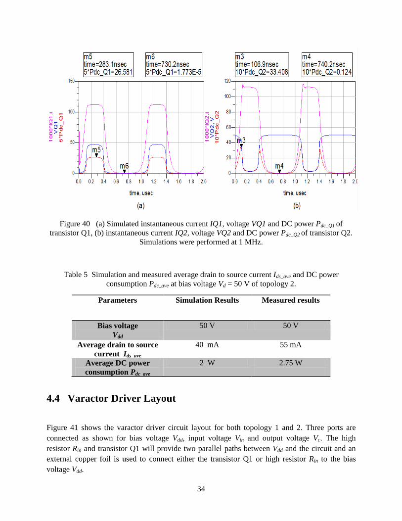
Figure 40 (a) shows the simulation results of instantaneous current IQ1, Voltage VQ1, DC power Pdc_Q1, current IQ2, voltage VQ2, and DC power Pdc_Q2 of transistor Q1, whereas figure 40 (b) shows the same characteristics for transistor Q2. Table 5 shows the measured and simulated average drain to source current Ids_ave and average DC power consumption Pdc_ave of driver circuit topology 2. The Pdc_ave = 2 W is more than the requirement of 1 W. This higher DC power consumption problem can be solved by using the transistor Q1 of the size of 1× 50µm2 or 2×25 µm2 in driver circuit topology 2. In that case we will achieve the average drain to source current Ids_ave = 15 mA and average DC power consumption Pdc_ave = 0.75 W less than the requirement of 1 W. Currently we used in this project work the transistor Q1 of the size 1× 200 µm2 due to minimum available size of batch 4 devices.
-15 -12.5 -10 -7.5 -5 -2.5 00
5
10
15
20
25
30
35
40
45
50
Driver input voltage Vin [V]
Driv
er o
utpu
t vol
tage
Vc
[V]
simulationmeasured
34
Figure 40 (a) Simulated instantaneous current IQ1, voltage VQ1 and DC power Pdc_Q1 of transistor Q1, (b) instantaneous current IQ2, voltage VQ2 and DC power Pdc_Q2 of transistor Q2.
Simulations were performed at 1 MHz.
Table 5 Simulation and measured average drain to source current Ids_ave and DC power consumption Pdc_ave at bias voltage Vd = 50 V of topology 2.
Parameters Simulation Results Measured results
Bias voltage Vdd
50 V 50 V
Average drain to source current Ids_ave
40 mA 55 mA
Average DC power consumption Pdc ave
2 W 2.75 W
4.4 Varactor Driver Layout
Figure 41 shows the varactor driver circuit layout for both topology 1 and 2. Three ports are connected as shown for bias voltage Vdd, input voltage Vin and output voltage Vc. The high resistor Rin and transistor Q1 will provide two parallel paths between Vdd and the circuit and an external copper foil is used to connect either the transistor Q1 or high resistor Rin to the bias voltage Vdd.

35
Figure 41 Layout of varactor driver circuit for both topology 1 and 2.
The varactor driver circuit is implemented in hybrid circuit using FR4 substrate of 1.5 mm thickness as shown in figure 42 below. Diced SiC MESFET are mounted on the fixture and wire bonded to the transmission line as shown in the zoom pictures of figure 42. The driver circuit size is 27×33 mm2.

36
4.5 Realistic Control Signal Measurement
Realistic control signal measurement is carried out for the driver circuit of topology 1 using oscilloscope and DC power supply. Driver circuit is loaded with a real DLM circuit as shown in figure 43 below and a real control signal that is already programed for high efficiency power amplifier in DLM application [7] is applied to the driver input and driver output voltage is observed through oscilloscope.
Vin Vdd=50V
Vc
Figure 42 Hybrid varactor driver circuit with diced SiC MESFET wire bonded to the transmission line.

37
Realistic control signal of 0.384 MHz and 4 MHz at a sampling frequency of 100 Msamples/s is used for the measurements. Figure 44 and 45 shows the driver input and output voltage at different samples for realistic control signal of 0.384 MHz bandwidth respectively. Figure 46 shows the expected and measured output voltage. It can be noticed that for 0.384 MHz bandwidth control signal the measured output voltage follow the expected output voltage correctly.
Vin Vdd=50V
Vc To Osc
Figure 43 Varactor driver circuit topology 1 is loaded with a real DLM circuit.

38
0 2000 4000 6000 8000 10000
-12
-10
-8
no. of samples [n]
Drive
r inpu
t volt
age
Vin
[V]
input voltage
0 2000 4000 6000 8000 1000020
25
30
35
40
no. of samples [n]
Drive
r out
put v
olta
ge V
c [V
]
measured output voltage
Figure 44 Varactor driver topology 1 input voltage vs. number of samples for realistic control signal of 0.384 MHz bandwidth.
Figure 45 Varactor driver topology 1 driver output voltage vs. number of samples for realistic control signal of 0.384 MHz bandwidth

39
Figure 46 Expected and measured driver output voltage at 0.384 MHz bandwidth control signal.
Figure 47 and 48 shows the varactor driver topology 1 input and output voltage for realistic control signal of 4 MHz bandwidth respectively. Figure 49 shows the varactor driver topology 1 expected and measured output voltage for 4 MHz bandwidth control signal. It can be noticed that the measured output voltage did not follow the expected output voltage because of the driver speed (bandwidth) limitation. The maximum speed of the varactor driver topology 1 is 1 MHz. However the varactor driver topology 2 can achieve speed of 10 MHz.
6000 6500 7000 7500 800024
26
28
30
32
34
36
expected output voltagemeasured output voltage

40
0 200 400 600 800 1000
-12
-10
-8
no. of samples [n]
Drive
r inpu
t volt
age
Vin
[V]
input voltage
0 200 400 600 800 100020
25
no. of samples [n]
Drive
r outp
ut vo
ltage
Vc
[V]
measured output voltage
Figure 47 Varactor driver topology 1 input voltage vs. number of samples for realistic control signal of 4 MHz bandwidth.
Figure 48 Varactor driver topology 1 driver output voltage vs. number of samples for realistic control signal of 4 MHz bandwidth.

41
Figure 49 Expected and measured varactor driver topology 1 output voltage at 4 MHz bandwidth control signal.
550 600 650 700 750 800
22
24
26
28
30
expected output voltagemeasured output voltage

42
Chapter 5
Conclusions and future work
In this thesis work a varactor driver circuit is designed and implemented with two types of topologies. The varactor driver maximum bandwidth (speed) of 1 MHz can be achieved with topology 1 and 10 MHz with topology 2. Varactor driver topology 1 is slower as compare to topology 2 because of a high resistor value Rin (1.8 kΩ) . The varactor driver circuit topology 2 has a steeper static transfer function as compare to topology 1, which means that a high range of driver output voltage can be changed by small change in driver input voltage. It is concluded that the varactor driver circuit topology 2 is better than topology 1 in terms of speed and static transfer function. However, topology 2 has a DC power consumption around 2 W whereas topology 1 only consumes 0.7 W which is less than the project requirement of 1 W. However, with a smaller size on the SiC MESFET Q1 (0.4×50 µm2) in varactor driver circuit topology 2 a DC power consumption of less than 1 W can be achieved, but with a bit slower driver speed.
As future work on this project more advance SiC MESFET models can be used to reduce the error between simulated and measured results of the varactor driver circuit. The maximum inductance of a MMIC inductor is 10 nH, which is a limitation in a MMIC implementation. A smaller inductor (10 nH) can be used by sacrificing the isolation between the anti-series varactors and the driver transistors (SiC MESFET). Finally a co-integrated version of a varactor driver circuit can be implemented in an advanced SiC MMIC process in the future.

43
Acknowledgements
I would like to express my gratitude to the people below for the completion of this project work.
First I would like to thank my examiner Associate professor Hans Hjelmgren and my supervisors Christer Andersson and Nicklas Ejebjörk for providing me the opportunity to work on this project. I am grateful for their valuable guidance, continuous support and excellent supervisions.
I have special thanks to Mustafa Özen for helping me with the measurements and layout of the printed circuit board. I would like to thank Olle Axelsson and Mattias Thorsell for their help in the project work whenever I needed. I appreciate their voluntary support.
My heartiest thanks to MEL staff for providing me social, friendly and educational environment throughout the project work.
I am thankful to my parents and friends for their encouragement and guidance throughout my educational life.
Finally, I am thankful to ALLAH for giving me the strength and ability to complete this project work.

44
References
[1] F. Raab, ‘‘High efficiency linear amplification by dynamic load modulation,’’ IEEE MTT-S int. Microw. Symp. Dig., jan.2003, pp.1717-1720
[2] F. Lepine, R. Jos, and H.Zirath, ‘‘A load modulated high efficiency power Amplifier,’’ Proc. 36th Eur. Microw. Conf., Sep. 2006, pp.411-414.
[3] H. M. Nemati, C. Fager, U. Gustavsson, H. Zirath, ‘‘Design of varactor-based tunable matching networks for dynamic load modulation of high power amplifiers,’’ IEEE Trans. Microwave Theory and Techniques, vol. 57, no. 5, May 2009.
[4] H. Hjelmgren, et. al., “Electro-thermal simulations of a microwave 4H-SiC MESFET on high purity semi-insulating substrate”, Solid-State Electronics, vol. 51 (2007) pp. 1144-1152
[5] C.M. Andersson, N. Ejebjörk, A. Henry, S. Andersson, E. Janzen, H. Zirath, and N. Rosman, “A SiC varactor with large effective tuning range for microwave power applications”, IEEE Electron Device Letters, vol. 32 no. 6 (2011) pp. 788-790
[6] C.M. Andersson, M. Thorsell and N. Rosman, “Nonlinear Characterization of Varactors for Tunable Networks by Active Source-Pull and Load-Pull”, IEEE Electron Device Letters, vol. 59 no. 7 (2011) pp. 1753-1760
[7] M. Özen, C. M. Andersson, Thomas Eriksson, M. Acar, R. Jos, and C. Fager, “High Efficiency RF Pulsewidth Modulation of Class-E Power Amplifiers,” IEEE Transactions on Microwave Theory and Techniques, vol.59, no.11, pp.2931-2942, Nov. 2011
[8] Steve C. Cripps, Advanced techniques in RF power amplifier design, Artec House, 2002 [9] Guillermo Gonzalez, Microwave Transistor Amplifier Analysis and Design, Prentic Hall,
1997

CHALMERS UNIVERSITY OF TECHNOLOGY SE-412 96 Göteborg, Sweden Phone: +46 (0) 31 772 10 00 Web: www.chalmers.se