Embed Size (px)
Citation preview
Page 1 of 28
DIODES, MICROWAVE, SILICON,
MULTIPLIER VARACTOR
BASED ON TYPES DH252, DH256, DH267, DH292
AND DH294
ESCC Detail Specification No. 5512/016
Issue 5 November 2014
Document Custodian: European Space Agency – see https://escies.org
ESCC Detail Specification No. 5512/016
PAGE 2
ISSUE 5
LEGAL DISCLAIMER AND COPYRIGHT
European Space Agency, Copyright © 2013. All rights reserved.
The European Space Agency disclaims any liability or responsibility, to any person or entity, with respect to any loss or damage caused, or alleged to be caused, directly or indirectly by the use and application of this ESCC publication.
This publication, without prior permission of the European Space Agency and provided it is not used for a commercial purpose, may be:
− copied in whole, in any medium, without alteration or modification. − copied in part, in any medium, provided that the ESCC document identification, comprising
the ESCC symbol, document number and document issue, is removed.

ESCC Detail Specification No. 5512/016
PAGE 3
ISSUE 5
DOCUMENTATION CHANGE NOTICE
(Refer to https://escies.org for ESCC DCR content)
DCR No. CHANGE DESCRIPTION
863 Specification upissued to incorporate editorial changes per DCR.

ESCC Detail Specification No. 5512/016
PAGE 4
ISSUE 5
TABLE OF CONTENTS
1 GENERAL 6
1.1 SCOPE 6
1.2 TYPE VARIANTS 6
1.3 MAXIMUM RATINGS 6
1.4 PARAMETER DERATING INFORMATION 6
1.5 PHYSICAL DIMENSIONS 6
1.6 FUNCTIONAL DIAGRAM 6
1.7 HANDLING PRECAUTIONS 6
2 APPLICABLE DOCUMENTS 6
3 TERMS, DEFINITIONS, ABBREVIATIONS, SYMBOLS AND UNITS 7
4 REQUIREMENTS 18
4.1 GENERAL 18
4.2 DEVIATIONS FROM GENERIC SPECIFICATION 18
4.2.1 Deviations from Production Control 18
4.2.2 Deviations from Final Production Tests (Chart II(b)) 18
4.2.3 Deviations from Burn-in and Electrical Measurements (Chart III(a)) 18
4.2.4 Deviations from Qualification Tests (Chart IV) 18
4.2.5 Deviations from Lot Acceptance Tests (Chart V) 19
4.3 MECHANICAL AND ENVIRONMENTAL REQUIREMENTS 19
4.3.1 Dimension Check 19
4.3.2 Weight 19
4.3.3 Terminal Strength 19
4.3.4 Bond Strength 19
4.3.5 Die Shear 19
4.3.6 High Temperature Stabilisation Bake 19
4.4 MATERIALS AND FINISHES 19
4.4.1 Case 20
4.4.2 Lead Materials and Finish 20
4.5 MARKING 20
4.5.1 General 20
4.5.2 Cathode Identification 20
4.5.3 The ESCC Component Number 20
4.5.4 Traceability Information 20
4.6 ELECTRICAL MEASUREMENTS 21
4.6.1 Electrical Measurements at Room Temperature 21

ESCC Detail Specification No. 5512/016
PAGE 5
ISSUE 5
4.6.2 Electrical Measurements at High and Low Temperatures 21
4.6.3 Circuits for Electrical Measurements 21
4.7 BURN-IN TESTS 21
4.7.1 Parameter Drift Values 21
4.7.2 Conditions for High Temperature Reverse Bias Burn-in 21
4.7.3 Conditions for Power Burn-in 21
4.7.4 Electrical Circuits for High Temperature Reverse Bias and Power Burn-in 21
4.8 ENVIRONMENTAL AND ENDURANCE TESTS (CHARTS IV AND V OF ESCC GENERIC SPECIFICATION NO. 5010) 27
4.8.1 Electrical Measurements on Completion of Environmental Tests 27
4.8.2 Electrical Measurements at Intermediate Points and on Completion of Endurance Tests 27
4.8.3 Conditions for Operating Life Tests (Part of Endurance Testing) 27
4.8.4 Electrical Circuits for Operating Life Tests 27
4.9 TOTAL DOSE IRRADIATION TESTING 27
4.10 SPECIAL TESTING 27
APPENDIX 'A' 28

ESCC Detail Specification No. 5512/016
PAGE 6
ISSUE 5
1 GENERAL
1.1 SCOPE This specification details the ratings, physical and electrical characteristics, test and inspection data for a Diode, Microwave, Silicon, Multiplier Varactor, based on Types DH252, DH256, DH267, DH292 and DH294. It shall be read in conjunction with ESCC Generic Specification No. 5010, the requirements of which are supplemented herein.
1.2 TYPE VARIANTS Variants of the basic diodes specified herein, which are also covered by this specification are given in Table 1(a).
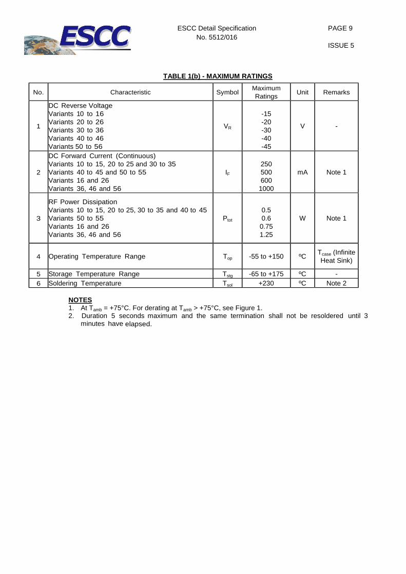
1.3 MAXIMUM RATINGS The maximum ratings, which shall not be exceeded at any time during use or storage, applicable to the diodes specified herein, are as scheduled in Table 1(b).
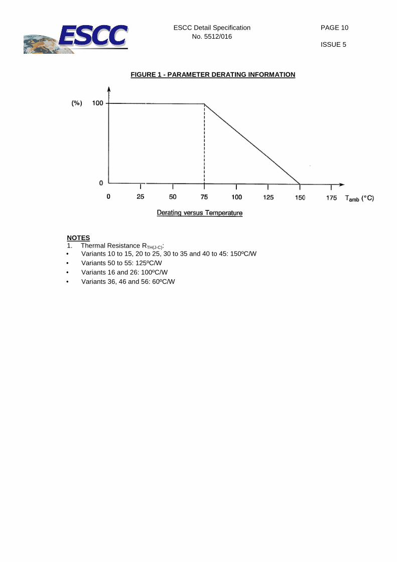
1.4 PARAMETER DERATING INFORMATION The derating information applicable to the diodes specified herein is shown in Figure 1.
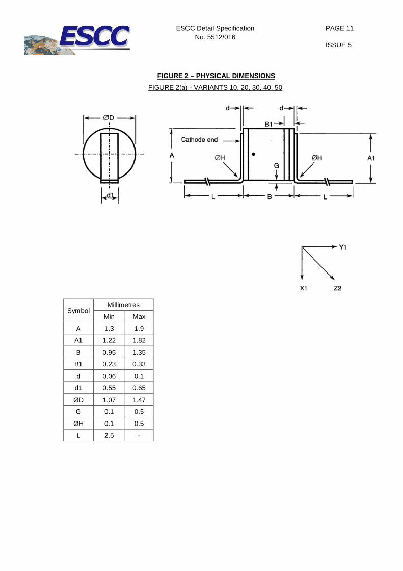
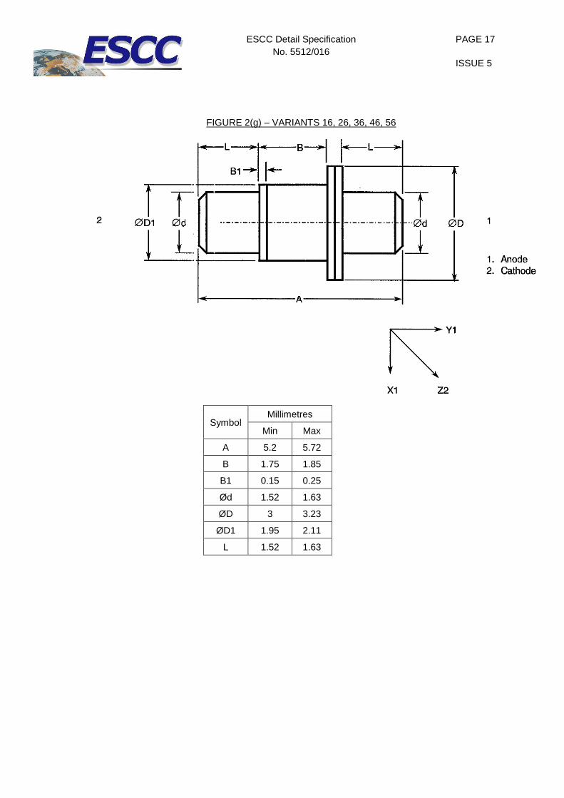
1.5 PHYSICAL DIMENSIONS The physical dimensions of the diodes specified herein are shown in Figure 2.
1.6 FUNCTIONAL DIAGRAM The functional diagram, showing lead identification, of the diodes specified herein, is shown in Figure 3.
1.7 HANDLING PRECAUTIONS These devices are susceptible to damage by electrostatic discharge. Therefore, suitable precautions shall be employed for protection during all phases of manufacture, testing, packaging, shipment and any handling.
These components are Categorised as Class 2 with a Minimum Critical Path Failure Voltage of 1550V.
2 APPLICABLE DOCUMENTS The following documents form part of this specification and shall be read in conjunction with it:
(a) ESCC Generic Specification No. 5010 for Discrete Microwave Semiconductor Components. (b) MIL-STD-750, Test Methods for Semiconductor Devices.

ESCC Detail Specification No. 5512/016
PAGE 7
ISSUE 5
3 TERMS, DEFINITIONS, ABBREVIATIONS, SYMBOLS AND UN ITS
For the purpose of this specification, the terms, definitions, abbreviations, symbols and units specified in ESCC Basic Specification No. 21300 shall apply. In addition the following symbols are used:
− CT = Total Capacitance
− τL = Minority Carrier Lifetime − tSO = Snap off Time
TABLE 1(a) – TYPE VARIANTS
(1) Variant
(2) Based On
Type
(3) Figure
(4) Total Capacitance
CT (pF) (Note 1)
(5) Output Power
Pout (W)
(6) Output
Frequency f0 (GHz)
(7) Body-Lid And Lead Material
And Finish
Min Max
10
DH267
2(a)
0.3 0.4 0.2 10-25
D7-E2
11 2(b) D7
12 2(c)
D7-E2 13 2(d)
14 2(e)
15 2(f)
16 2(g) 0.4 0.5 A7-D7
20
DH292
2(a)
0.3 0.6 0.6 8-16
D7-E2
21 2(b) D7
22 2(c)
D7-E2 23 2(d)
24 2(e)
25 2(f)
26 2(g) 0.4 0.7 A7-D7
30
DH256
2(a)
0.6 1.2 2.0 5-12
D7-E2
31 2(b) D7
32 2(c)
D7-E2 33 2(d)
34 2(e)
35 2(f)
36 2(g) 0.7 1.3 A7-D7

ESCC Detail Specification No. 5512/016
PAGE 8
ISSUE 5
(1)
Variant (2)
Based On Type
(3) Figure
(4) Total Capacitance
CT (pF) (Note 1)
(5) Output Power
Pout (W)
(6) Output
Frequency f0 (GHz)
(7) Body-Lid And Lead Material
And Finish
Min Max
40
DH252
2(a)
1 2.1 3.0 2-8
D7-E2
41 2(b) D7
42 2(c)
D7-E2 43 2(d)
44 2(e)
45 2(f)
46 2(g) 1.1 2.2 A7-D7
50
DH294
2(a)
4.1 7.1 0.5
0.2-2
D7-E2
51 2(b) D7
52 2(c)
D7-E2 53 2(d)
54 2(e)
55 2(f)
56 2(g) 4.2 7.2 A7-D7
NOTES 1. VR = -6.0V, f = 1.0MHz.
ESCC Detail Specification No. 5512/016
PAGE 9
ISSUE 5
TABLE 1(b) - MAXIMUM RATINGS
No. Characteristic Symbol Maximum Ratings
Unit Remarks
1
DC Reverse Voltage Variants 10 to 16 Variants 20 to 26 Variants 30 to 36 Variants 40 to 46 Variants 50 to 56
VR
-15 -20 -30 -40 -45
V -
2
DC Forward Current (Continuous) Variants 10 to 15, 20 to 25 and 30 to 35 Variants 40 to 45 and 50 to 55 Variants 16 and 26 Variants 36, 46 and 56
IF
250 500 600 1000
mA Note 1
3
RF Power Dissipation Variants 10 to 15, 20 to 25, 30 to 35 and 40 to 45 Variants 50 to 55 Variants 16 and 26 Variants 36, 46 and 56
Ptot
0.5 0.6 0.75 1.25
W Note 1
4 Operating Temperature Range Top -55 to +150 ºC Tcase (Infinite Heat Sink)
5 Storage Temperature Range Tstg -65 to +175 ºC - 6 Soldering Temperature Tsol +230 ºC Note 2
NOTES 1. At Tamb = +75°C. For derating at Tamb > +75°C, see Figure 1. 2. Duration 5 seconds maximum and the same termination shall not be resoldered until 3
minutes have elapsed.
ESCC Detail Specification No. 5512/016
PAGE 10
ISSUE 5
FIGURE 1 - PARAMETER DERATING INFORMATION
NOTES 1. Thermal Resistance RTH(J-C): • Variants 10 to 15, 20 to 25, 30 to 35 and 40 to 45: 150ºC/W • Variants 50 to 55: 125ºC/W • Variants 16 and 26: 100ºC/W • Variants 36, 46 and 56: 60ºC/W
ESCC Detail Specification No. 5512/016
PAGE 11
ISSUE 5
FIGURE 2 – PHYSICAL DIMENSIONS
FIGURE 2(a) - VARIANTS 10, 20, 30, 40, 50
Symbol Millimetres
Min Max
A 1.3 1.9
A1 1.22 1.82
B 0.95 1.35
B1 0.23 0.33
d 0.06 0.1
d1 0.55 0.65
ØD 1.07 1.47
G 0.1 0.5
ØH 0.1 0.5
L 2.5 -

ESCC Detail Specification No. 5512/016
PAGE 12
ISSUE 5
FIGURE 2(b) - VARIANTS 11, 21, 31, 41, 51
Symbol Millimetres
Min Max
B 0.95 1.35
B1 0.23 0.33
ØD 1.07 1.47

ESCC Detail Specification No. 5512/016
PAGE 13
ISSUE 5
FIGURE 2(c) – VARIANTS 12, 22, 32, 42, 52
Symbol Millimetres
Min Max
A1 0.99 1.39
B 0.95 1.35
B1 0.23 0.33
d 0.06 0.1
d1 0.55 0.65
ØD 1.07 1.47
L 5 -

ESCC Detail Specification No. 5512/016
PAGE 14
ISSUE 5
FIGURE 2(d) – VARIANTS 13, 23, 33, 43, 53
Symbol Millimetres
Min Max
A1 0.99 1.39
B 0.95 1.35
B1 0.23 0.33
d 0.06 0.1
d1 0.55 0.65
ØD 1.07 1.47
L 5 -

ESCC Detail Specification No. 5512/016
PAGE 15
ISSUE 5
FIGURE 2(e) – VARIANTS 14, 24, 34, 44, 54
Symbol Millimetres
Min Max
A1 0.99 1.39
B 0.95 1.35
B1 0.23 0.33
d 0.06 0.1
d1 0.55 0.65
ØD 1.07 1.47
L 5 -

ESCC Detail Specification No. 5512/016
PAGE 16
ISSUE 5
FIGURE 2(f) – VARIANTS 15, 25, 35, 45, 55
Symbol Millimetres
Min Max
B 0.95 1.35
B1 0.23 0.33
C 10 10.4
d 0.06 0.1
d1 0.55 0.65
ØD 1.07 1.47
L 5 -
ESCC Detail Specification No. 5512/016
PAGE 17
ISSUE 5
FIGURE 2(g) – VARIANTS 16, 26, 36, 46, 56
Symbol Millimetres
Min Max
A 5.2 5.72
B 1.75 1.85
B1 0.15 0.25
Ød 1.52 1.63
ØD 3 3.23
ØD1 1.95 2.11
L 1.52 1.63

ESCC Detail Specification No. 5512/016
PAGE 18
ISSUE 5
FIGURE 3 – FUNCTIONAL DIAGRAM
NOTES 1. The cathode end shall be marked with a black dot. The marking will not be on the cathode
connection but adjacent to it except for the case in Figure 2(g).
4 REQUIREMENTS
4.1 GENERAL The complete requirements for procurement of the diodes specified herein are stated in this specification and ESCC Generic Specification No. 5010 for discrete Microwave Semiconductor Components. Deviations from the Generic Specification, applicable to this specification only, are listed in Para. 4.2.
Deviations from the applicable Generic Specification and this Detail Specification, formally agreed with specific Manufacturers on the basis that the alternative requirements are equivalent to the ESCC requirements and do not affect the components' reliability, are listed in the appendices attached to this specification.
4.2 DEVIATIONS FROM GENERIC SPECIFICATION
4.2.1 Deviations from Production Control
(a) Para. 5.3, Wafer Lot Acceptance: Minority Carrier Lifetime (τL) and Snap Off Time (tSO) shall
be performed on wafer acceptance best parts. 27 die on wafer for τL and 20 packaged diodes for tSO.
4.2.2 Deviations from Final Production Tests (Chart II(b)) None.
4.2.3 Deviations from Burn-in and Electrical Measurements (Chart III(a)) None.
4.2.4 Deviations from Qualification Tests (Chart IV) (a) Para. 9.13, Shock Test: Shall not be performed. (b) Para. 9.14, Vibration: Shall not be performed. (c) Para. 9.15, Constant Acceleration: Shall not be performed. (d) Para. 9.19, Terminal Strength: Shall not be performed for Variants 11, 16, 21, 26, 31, 36, 41,
46, 51 and 56. (e) Para. 9.23, Special Testing: Shall not be performed.
ESCC Detail Specification No. 5512/016
PAGE 19
ISSUE 5
4.2.5 Deviations from Lot Acceptance Tests (Chart V)
(a) Para. 9.13, Shock Test: Shall not be performed. (b) Para. 9.14, Vibration: Shall not be performed. (c) Para. 9.15, Constant Acceleration: Shall not be performed. (d) Para. 9.19, Terminal Strength: Shall not be performed for Variants 11, 16, 21, 26, 31, 36, 41,
46, 51 and 56. (e) Para. 9.23, Special Testing: Shall not be performed.
4.3 MECHANICAL AND ENVIRONMENTAL REQUIREMENTS
4.3.1 Dimension Check The dimensions of the diodes specified herein shall be checked. They shall conform to those shown in Figure 2.
4.3.2 Weight The maximum weight of the diodes specified herein shall be as follows:
− Variants 10 to 15, 20 to 25, 30 to 35, 40 to 45 and 50 to 55: 0.02g. − Variants 16, 26, 36, 46 and 56: 0.15g.
4.3.3 Terminal Strength The requirements for terminal strength testing are specified in Section 9 of ESCC Generic Specification No. 5010. The test conditions shall be as follows:
(a) Condition: 'A' (Tension) Variants 10, 12 to 15, 20, 22 to 25, 30, 32 to 35, 40, 42 to 45, 50 and 52 to 55:
− Force: 1.25N − Duration: 10 seconds.
4.3.4 Bond Strength The requirements for bond strength are specified in Section 9 of ESCC Generic Specification No. 5010. The test conditions shall be as follows:
(a) Condition: 'A' (tension). (b) Separating Force: 0.03N minimum.
4.3.5 Die Shear The requirements for die shear are specified in Section 9 of ESCC Generic Specification No. 5010. The test conditions shall be as follows:-
(a) Semiconductor material remaining: 50% minimum.
4.3.6 High Temperature Stabilisation Bake The requirements for high temperature stabilisation bake are specified in Section 9 of ESCC Generic Specification No. 5010. The temperature to be applied shall be +175 (+0 -3)ºC.
4.4 MATERIALS AND FINISHES The materials and finishes shall be as specified herein. Where a definite material is not specified, a material which will enable the diodes specified herein to meet the performance requirements of this specification shall be used. Acceptance or approval of any constituent material shall not guarantee acceptance of the finished product.
ESCC Detail Specification No. 5512/016
PAGE 20
ISSUE 5
4.4.1 Case
The case shall be hermetically sealed and have a ceramic body. The lid shall be welded or preform soldered.
4.4.2 Lead Materials and Finish (a) For Variants 10 to 15, 20 to 25, 30 to 35, 40 to 45 and 50 to 55, the body material shall be
Type 'D' with Type '7' finish and the lid material shall be Type 'E' with Type '2' finish, in accordance with the requirements of ESCC Basic Specification No. 23500.
(b) For Variants 16, 26, 36, 46 and 56, the body material shall be Type 'A' with Type '7' finish and the lid material shall be Type 'D' with Type '7' finish, in accordance with the requirements of ESCC Basic specification No. 23500.
4.5 MARKING
4.5.1 General The marking of components delivered to this specification shall be in accordance with the requirements of ESCC Basic Specification No. 21700 and the following paragraphs. When the component is too small to accommodate all of the marking specified, as much as space permits shall be marked and the marking information, in full, shall accompany the component in its primary package.
The information to be marked and the order of precedence, shall be as follows:-
(a) Cathode Identification. (b) The ESCC Component Number. (c) Traceability Information.
4.5.2 Cathode Identification Cathode identification shall be as shown in Figures 2 and 3 of this specification.
4.5.3 The ESCC Component Number Each component shall bear the ESCC Component Number which shall be constituted and marked as follows:
Example: 551201610BF
• Detail Specification Number: 5512016 • Type Variant (see Table 1(a)): 10 • Testing Level (B or C, as applicable): B • Total Dose Irradiation Level (if applicable): F
The Total Dose Irradiation Level designation shall be added for those devices for which a sample has been successfully tested to the level in question. For these devices, a code letter shall be added in accordance with the requirements of ESCC Basic Specification No. 22900.
4.5.4 Traceability Information Each component shall be marked in respect of traceability information as defined in ESCC Basic Specification No. 21700.

ESCC Detail Specification No. 5512/016
PAGE 21
ISSUE 5
4.6 ELECTRICAL MEASUREMENTS
4.6.1 Electrical Measurements at Room Temperature The parameters to be measured at room temperature are scheduled in Table 2. Unless otherwise specified, the measurements shall be performed at Tamb = +22 ±3°C.
4.6.2 Electrical Measurements at High and Low Temperatures The parameters to be measured at high and low temperatures are scheduled in Table 3. Unless otherwise specified, the measurements shall be performed at Tamb = +150 (+0 -3)ºC.
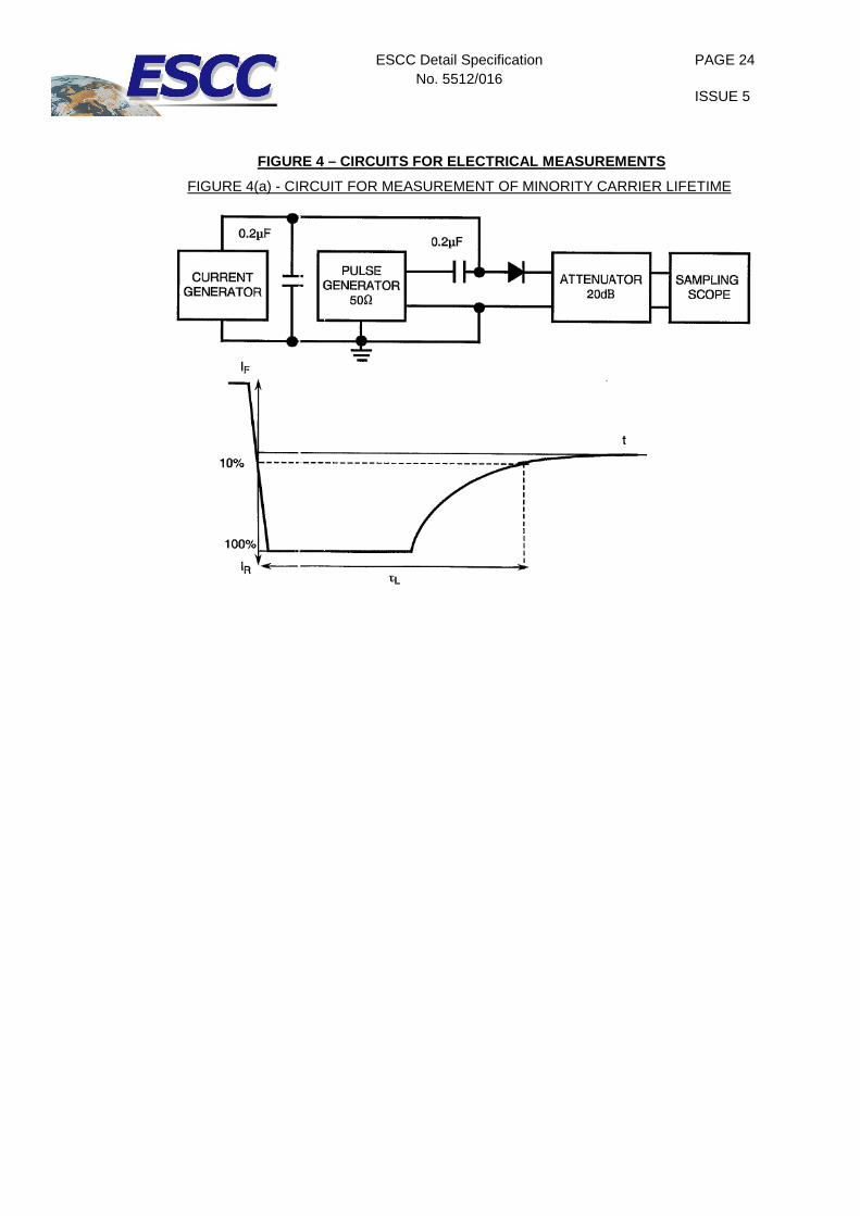
4.6.3 Circuits for Electrical Measurements Circuits for use in performing electrical measurements listed in Table 2 of this specification are shown in Figure 4.
4.7 BURN-IN TESTS Burn-in shall be Category 2 of Chart III(a) of ESCC Generic Specification No. 5010.
4.7.1 Parameter Drift Values The parameter drift values applicable to burn-in are specified in Table 4 of this specification. Unless otherwise stated, the measurements shall be performed at Tamb = +22 ±3ºC. The parameter drift values (∆) applicable to the scheduled parameters shall not be exceeded. In addition to these drift value requirements for a given parameter, the appropriate limit value specified in Table 2 shall not be exceeded.
4.7.2 Conditions for High Temperature Reverse Bias Burn-in The requirements for the high temperature reverse bias burn-in are specified in Section 9 of ESCC Generic Specification No. 5010. The conditions for high temperature reverse bias burn-in shall be as specified in Table 5(a) of this specification.
4.7.3 Conditions for Power Burn-in The requirements for power burn-in are specified in Section 9 of ESCC Generic Specification No. 5010. The conditions for power burn-in shall be as specified in Table 5(b) of this specification.
4.7.4 Electrical Circuits for High Temperature Reverse Bias and Power Burn-in Circuits for use in performing the H.T.R.B and power burn-in tests are shown in Figures 5(a) and 5(b) of this specification.

ESCC Detail Specification No. 5512/016
PAGE 22
ISSUE 5
TABLE 2 – ELECTRICAL MEASUREMENTS AT ROOM TEMPERATU RE – DC PARAMETERS
No. Characteristics Symbol MIL-STD-750 Test Method
Test Conditions Limits Unit
Min. Max.
1 Breakdown Voltage VBR 4021 IR = 10µA
V
Variants 10 to 16 -15 -
Variants 20 to 26 -20 -
Variants 30 to 36 -30 -
Variants 40 to 46 -40 -
Variants 50 to 56 -45 -70
2 Reverse Current IR 4016 VR = -10V - 20 nA
3 Forward Voltage VF 4011 IF = 10mA - 1.1 V
TABLE 2 – ELECTRICAL MEASUREMENTS AT ROOM TEMPERATU RE – AC PARAMETERS
No. Characteristics
Symbol
MIL-STD-750 Test Method
Test Fig. Test Conditions
Limits
Unit Min. Max.
4 Total Capacitance CT 4001 - VR = -6.0V f = 1.0MHz
Note 1 pF
5 Minority Carrier Lifetime Note 2
τL - 4(a) IF = 10mA
IR = 6mA Variants 10 to 16 Variants 20 to 26 Variants 30 to 36 Variants 40 to 46 Variants 50 to 56
6 10 20 35 125
- - - - -
ns
6 Snap Off Time Note 2
tSO - 4(b) IF = 10mA VR = 10V
Variants 10 to 16 Variants 20 to 26 Variants 30 to 36 Variants 40 to 46 Variants 50 to 56
- - - - -
60 75 120 200 400
ps
NOTES 1. See Column 4 of Table 1(a). 2. Only on wafer acceptance test parts.

ESCC Detail Specification No. 5512/016
PAGE 23
ISSUE 5
TABLE 3 - ELECTRICAL MEASUREMENTS AT HIGH AND LOW T EMPERATURES
No. Characteristics Symbol MIL-STD-750 Test
Method Test Conditions
Limits Unit
Min. Max.
2 Reverse Current 2 IR 4016 VR = -10V - 1 µA
TABLE 4 - PARAMETER DRIFT VALUES
No. Characteristics Symbol Spec. And/Or Test
Method Test Conditions
Change Limits (∆)
Unit
2 Reverse Current IR As per Table 2 As per Table 2 ±5 (1) or (2)
±100 (1)
nA
%
3 Forward Voltage VF As per Table 2 As per Table 2 ±5 (1) %
4 Total Capacitance CT As per Table 2 As per Table 2 ±5 (1) (3) %
NOTES 1. ∆1 = ∆2. 2. Whichever is the greater, referred to the initial measurement. 3. Rounded upwards to nearest 0.01pF value. If CT ≤ 0.50pF then ∆=±10%.
ESCC Detail Specification No. 5512/016
PAGE 24
ISSUE 5
FIGURE 4 – CIRCUITS FOR ELECTRICAL MEASUREMENTS
FIGURE 4(a) - CIRCUIT FOR MEASUREMENT OF MINORITY CARRIER LIFETIME
ESCC Detail Specification No. 5512/016
PAGE 25
ISSUE 5
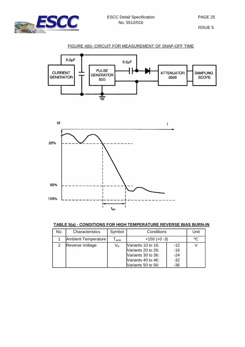
FIGURE 4(b)- CIRCUIT FOR MEASUREMENT OF SNAP-OFF TIME
TABLE 5(a) - CONDITIONS FOR HIGH TEMPERATURE REVERS E BIAS BURN-IN
No. Characteristics Symbol Conditions Unit
1 Ambient Temperature Tamb +150 (+0 -3) ºC
2 Reverse Voltage VR Variants 10 to 16: Variants 20 to 26: Variants 30 to 36: Variants 40 to 46: Variants 50 to 56:
-12 -16 -24 -32 -36
V

ESCC Detail Specification No. 5512/016
PAGE 26
ISSUE 5
TABLE 5(b) - CONDITIONS FOR POWER BURN-IN AND OPERA TING LIFE TEST
No. Characteristics Symbol Conditions Unit
1 Ambient Temperature Tamb +125 (+0 -3) ºC
2 Forward Current IF Variants 10 to 16, 20 to 26, 30 to 35: Variants 40 to 45, 50 to 55: Variants 36 and 46: Variant 56:
50 50 120 130
mA
FIGURE 5(a)- ELECTRICAL CIRCUIT FOR HIGH TEMPERATUR E REVERSE BIAS BURN-IN
NOTES 1. At the end of the HTRB, Tamb shall be decreased to room temperature and the reverse bias
shall remain applied until Tamb < +35ºC.
FIGURE 5(b) - ELECTRICAL CIRCUIT FOR POWER BURN-IN AND OPERATING LIFE TESTS
ESCC Detail Specification No. 5512/016
PAGE 27
ISSUE 5
4.8 ENVIRONMENTAL AND ENDURANCE TESTS (CHARTS IV AND V OF ESCC GENERIC
SPECIFICATION No. 5010)
4.8.1 Electrical Measurements on Completion of Environmental Tests The parameters to be measured on completion of environmental tests are scheduled in Table 2. Unless otherwise stated, the measurements shall be performed at Tamb = +22 ±3ºC.
4.8.2 Electrical Measurements at Intermediate Points and on Completion of Endurance Tests The parameters to be measured at intermediate points and on completion of endurance tests are scheduled in Table 6. Unless otherwise stated, the measurements shall be performed at Tamb = +22 ±3°C.
4.8.3 Conditions for Operating Life Tests (Part of Endurance Testing) The requirements for operating life testing are specified in Section 9 of ESCC Generic Specification No. 5010. The conditions for operating life testing are specified in Table 5(b) of this specification.
4.8.4 Electrical Circuits for Operating Life Tests The circuit to be used for performance of the operating life test shall be the same as shown in Figure 5(b) for Power Burn-in.
4.9 TOTAL DOSE IRRADIATION TESTING Not applicable.
4.10 SPECIAL TESTING Not applicable.
TABLE 6 – MEASUREMENTS AT INTERMEDIATE POINTS AND O N COMPLETION OF ENDURANCE TESTING
No. Characteristics Symbol Spec. And/Or Test
Method Test Conditions
Limits Unit
Min. Max.
1 Breakdown Voltage VBR As per Table 2 As per Table 2 As per Table 2 V
2 Reverse Current IR As per Table 2 As per Table 2 As per Table 2 nA
3 Forward Voltage VF As per Table 2 As per Table 2 As per Table 2 V
4 Total Capacitance CT As per Table 2 As per Table 2 As per Table 2 pF

ESCC Detail Specification No. 5512/016
PAGE 28
ISSUE 5
APPENDIX A
AGREED DEVIATIONS FOR COBHAM MICROWAVE (F)
ITEMS AFFECTED DESCRIPTION OF DEVIATIONS
Para. 4.2.1 Para. 5.2, Wafer Lot Acceptance: Scanning Electron Microscope (SEM) Inspection shall be performed on one wafer per metallisation run. Three dice shall be selected at random after dicing.
Para. 4.2.2 Para. 9.12, Radiographic Inspection of Chart IIl(a): May be performed after Para. 9.7, PIND test.
Para. 4.2.3 Para. 9.1.2, Radiographic Inspection: May be performed after Para. 9.7, PIND test of Chart II(b).


![· Varactor (also called varicap, VVC [voltage-variable capacitance], or tuning) diodes are semiconductor, voltage-dependent, variable capacitors. Their mode of operation depends](https://img.dokumen.tips/doc/110x75/5e86c547b953eb1d5317e2e3/varactor-also-called-varicap-vvc-voltage-variable-capacitance-or-tuning-diodes.jpg)


![· Varactor (also called varicap, WC [voltage-variable capacitance], or tuning) diodes are semiconductor, voltage-dependent, variable capacitors. Their mode of operation depends](https://img.dokumen.tips/doc/110x75/5e86c5ba62ce4471a605cd80/varactor-also-called-varicap-wc-voltage-variable-capacitance-or-tuning-diodes.jpg)