Embed Size (px)
Citation preview
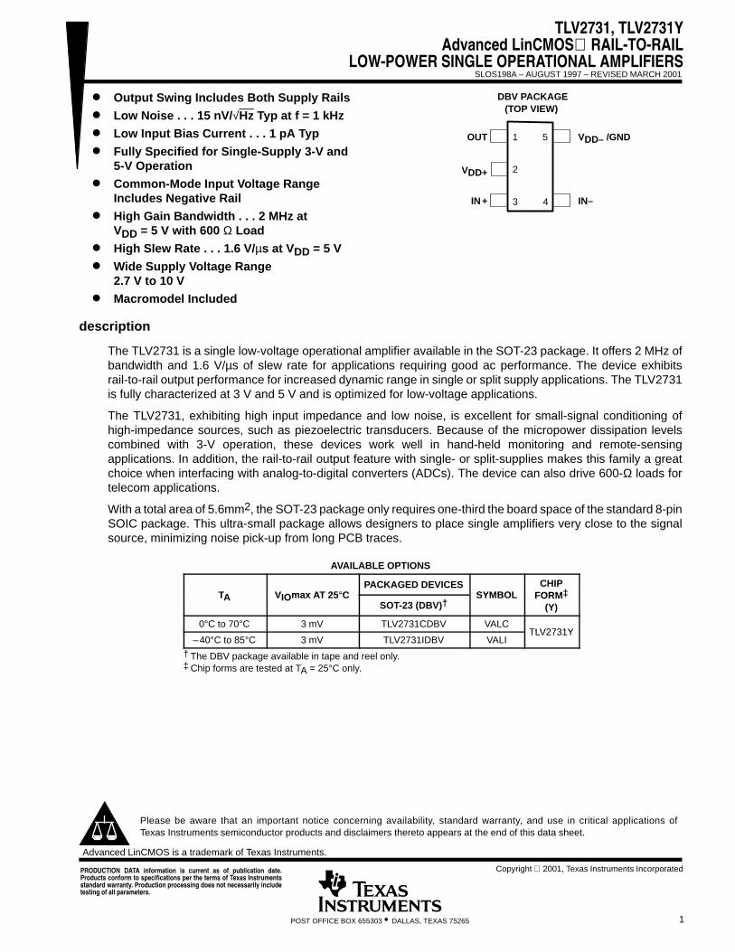
TLV2731, TLV2731YAdvanced LinCMOS RAIL-TO-RAIL
LOW-POWER SINGLE OPERATIONAL AMPLIFIERS
SLOS198A – AUGUST 1997 – REVISED MARCH 2001
1POST OFFICE BOX 655303 • DALLAS, TEXAS 75265
Output Swing Includes Both Supply Rails
Low Noise . . . 15 nV/√Hz Typ at f = 1 kHz
Low Input Bias Current . . . 1 pA Typ
Fully Specified for Single-Supply 3-V and5-V Operation
Common-Mode Input Voltage RangeIncludes Negative Rail
High Gain Bandwidth . . . 2 MHz at VDD = 5 V with 600 Ω Load
High Slew Rate . . . 1.6 V/µs at VDD = 5 V
Wide Supply Voltage Range2.7 V to 10 V
Macromodel Included
description
The TLV2731 is a single low-voltage operational amplifier available in the SOT-23 package. It offers 2 MHz ofbandwidth and 1.6 V/µs of slew rate for applications requiring good ac performance. The device exhibitsrail-to-rail output performance for increased dynamic range in single or split supply applications. The TLV2731is fully characterized at 3 V and 5 V and is optimized for low-voltage applications.
The TLV2731, exhibiting high input impedance and low noise, is excellent for small-signal conditioning ofhigh-impedance sources, such as piezoelectric transducers. Because of the micropower dissipation levelscombined with 3-V operation, these devices work well in hand-held monitoring and remote-sensingapplications. In addition, the rail-to-rail output feature with single- or split-supplies makes this family a greatchoice when interfacing with analog-to-digital converters (ADCs). The device can also drive 600-Ω loads fortelecom applications.
With a total area of 5.6mm2, the SOT-23 package only requires one-third the board space of the standard 8-pinSOIC package. This ultra-small package allows designers to place single amplifiers very close to the signalsource, minimizing noise pick-up from long PCB traces.
AVAILABLE OPTIONS
TA VIOmax AT 25°CPACKAGED DEVICES
SYMBOLCHIP
FORM‡TA VIOmax AT 25°CSOT-23 (DBV)†
SYMBOL FORM‡
(Y)
0°C to 70°C 3 mV TLV2731CDBV VALCTLV2731Y
–40°C to 85°C 3 mV TLV2731IDBV VALITLV2731Y
† The DBV package available in tape and reel only.‡ Chip forms are tested at TA = 25°C only.
Please be aware that an important notice concerning availability, standard warranty, and use in critical applications ofTexas Instruments semiconductor products and disclaimers thereto appears at the end of this data sheet.
DBV PACKAGE(TOP VIEW)
5
43
1
2
IN+
VDD+
OUT VDD– /GND
IN–
PRODUCTION DATA information is current as of publication date.Products conform to specifications per the terms of Texas Instrumentsstandard warranty. Production processing does not necessarily includetesting of all parameters.
Copyright 2001, Texas Instruments Incorporated
Advanced LinCMOS is a trademark of Texas Instruments.
TLV2731, TLV2731YAdvanced LinCMOS RAIL-TO-RAILLOW-POWER SINGLE OPERATIONAL AMPLIFIERS
SLOS198A – AUGUST 1997 – REVISED MARCH 2001
2 POST OFFICE BOX 655303 • DALLAS, TEXAS 75265
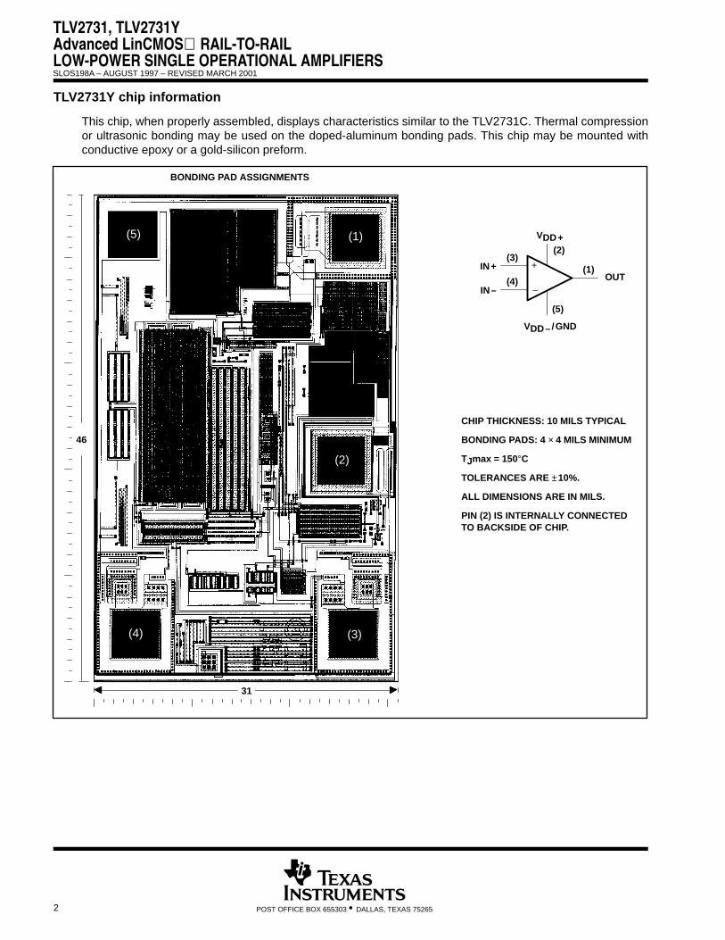
TLV2731Y chip information
This chip, when properly assembled, displays characteristics similar to the TLV2731C. Thermal compressionor ultrasonic bonding may be used on the doped-aluminum bonding pads. This chip may be mounted withconductive epoxy or a gold-silicon preform.
BONDING PAD ASSIGNMENTS
CHIP THICKNESS: 10 MILS TYPICAL
BONDING PADS: 4 × 4 MILS MINIMUM
TJmax = 150°C
TOLERANCES ARE ±10%.
ALL DIMENSIONS ARE IN MILS.
PIN (2) IS INTERNALLY CONNECTEDTO BACKSIDE OF CHIP.
+
–OUT
IN+
IN–
VDD+(2)
(3)
(4)(1)
(5)
VDD– /GND
46
(3)
(2)
(1)(5)
(4)
31
TLV2731, TLV2731YAdvanced LinCMOS RAIL-TO-RAIL
LOW-POWER SINGLE OPERATIONAL AMPLIFIERS
SLOS198A – AUGUST 1997 – REVISED MARCH 2001
3POST OFFICE BOX 655303 • DALLAS, TEXAS 75265
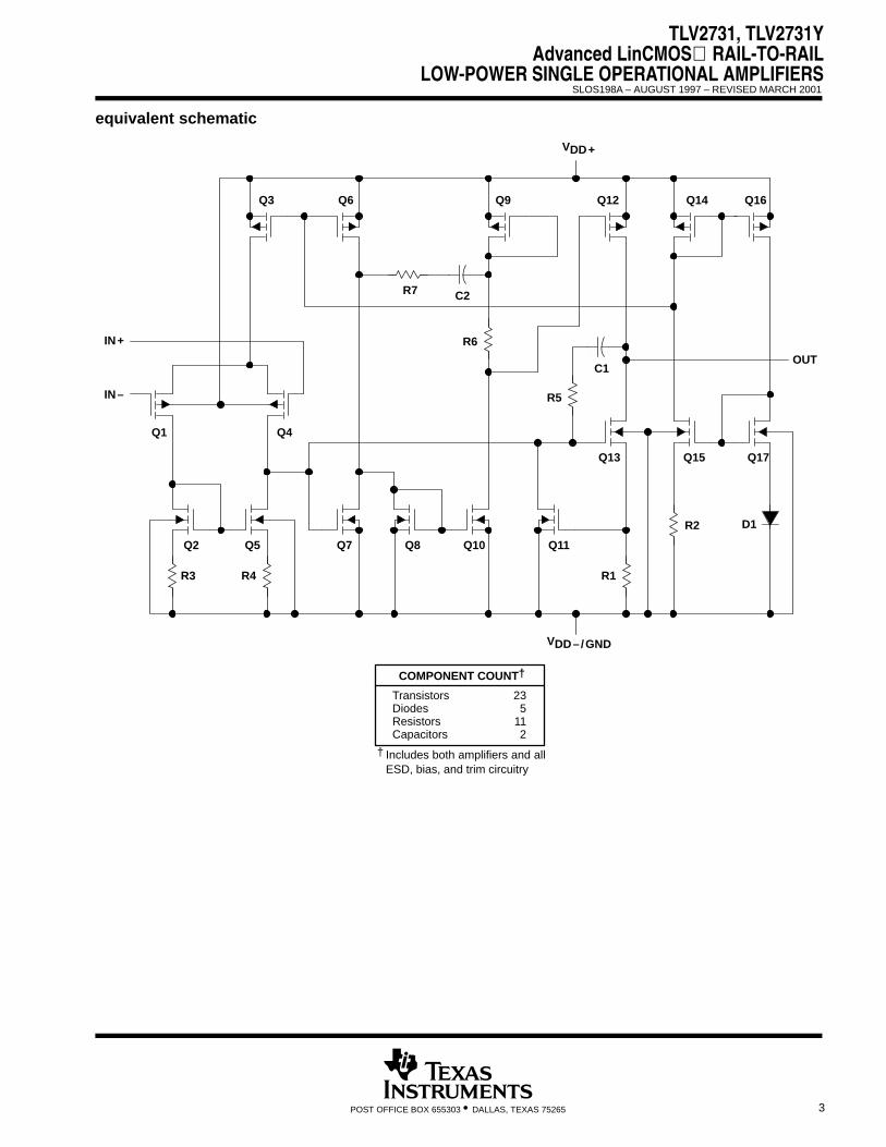
equivalent schematic
Q3 Q6 Q9 Q12 Q14 Q16
Q2 Q5 Q7 Q8 Q10 Q11
D1
Q17Q15Q13
Q4Q1
R5
C1
VDD+
IN+
IN–
R3
R7
R1
R2
OUT
VDD– /GND
COMPONENT COUNT†
TransistorsDiodesResistorsCapacitors
23 511 2
† Includes both amplifiers and allESD, bias, and trim circuitry
R6
C2
R4
TLV2731, TLV2731YAdvanced LinCMOS RAIL-TO-RAILLOW-POWER SINGLE OPERATIONAL AMPLIFIERS
SLOS198A – AUGUST 1997 – REVISED MARCH 2001
4 POST OFFICE BOX 655303 • DALLAS, TEXAS 75265
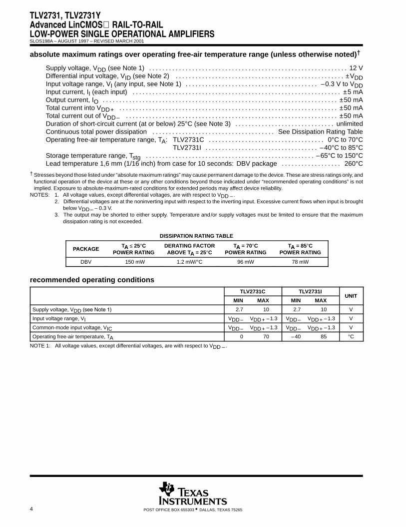
absolute maximum ratings over operating free-air temperature range (unless otherwise noted)†
Supply voltage, VDD (see Note 1) 12 V. . . . . . . . . . . . . . . . . . . . . . . . . . . . . . . . . . . . . . . . . . . . . . . . . . . . . . . . . . . . Differential input voltage, VID (see Note 2) ±VDD. . . . . . . . . . . . . . . . . . . . . . . . . . . . . . . . . . . . . . . . . . . . . . . . . . . Input voltage range, VI (any input, see Note 1) –0.3 V to VDD. . . . . . . . . . . . . . . . . . . . . . . . . . . . . . . . . . . . . . . . Input current, II (each input) ±5 mA. . . . . . . . . . . . . . . . . . . . . . . . . . . . . . . . . . . . . . . . . . . . . . . . . . . . . . . . . . . . . . . Output current, IO ±50 mA. . . . . . . . . . . . . . . . . . . . . . . . . . . . . . . . . . . . . . . . . . . . . . . . . . . . . . . . . . . . . . . . . . . . . . . Total current into VDD+ ±50 mA. . . . . . . . . . . . . . . . . . . . . . . . . . . . . . . . . . . . . . . . . . . . . . . . . . . . . . . . . . . . . . . . . . Total current out of VDD– ±50 mA. . . . . . . . . . . . . . . . . . . . . . . . . . . . . . . . . . . . . . . . . . . . . . . . . . . . . . . . . . . . . . . . Duration of short-circuit current (at or below) 25°C (see Note 3) unlimited. . . . . . . . . . . . . . . . . . . . . . . . . . . . . . Continuous total power dissipation See Dissipation Rating Table. . . . . . . . . . . . . . . . . . . . . . . . . . . . . . . . . . . . . Operating free-air temperature range, TA: TLV2731C 0°C to 70°C. . . . . . . . . . . . . . . . . . . . . . . . . . . . . . . . . . .
TLV2731I –40°C to 85°C. . . . . . . . . . . . . . . . . . . . . . . . . . . . . . . . . . Storage temperature range, Tstg –65°C to 150°C. . . . . . . . . . . . . . . . . . . . . . . . . . . . . . . . . . . . . . . . . . . . . . . . . . . Lead temperature 1,6 mm (1/16 inch) from case for 10 seconds: DBV package 260°C. . . . . . . . . . . . . . . . . .
† Stresses beyond those listed under “absolute maximum ratings” may cause permanent damage to the device. These are stress ratings only, andfunctional operation of the device at these or any other conditions beyond those indicated under “recommended operating conditions” is notimplied. Exposure to absolute-maximum-rated conditions for extended periods may affect device reliability.
NOTES: 1. All voltage values, except differential voltages, are with respect to VDD – .2. Differential voltages are at the noninverting input with respect to the inverting input. Excessive current flows when input is brought
below VDD– – 0.3 V.3. The output may be shorted to either supply. Temperature and /or supply voltages must be limited to ensure that the maximum
dissipation rating is not exceeded.
DISSIPATION RATING TABLE
PACKAGETA ≤ 25°C DERATING FACTOR TA = 70°C TA = 85°C
PACKAGE APOWER RATING ABOVE TA = 25°C
APOWER RATING
APOWER RATING
DBV 150 mW 1.2 mW/°C 96 mW 78 mW
recommended operating conditions
TLV2731C TLV2731IUNIT
MIN MAX MIN MAXUNIT
Supply voltage, VDD 2.7 10 2.7 10 V
Input voltage range, VI VDD– VDD+ –1.3 VDD– VDD+ –1.3 V
Common-mode input voltage, VIC VDD– VDD+ –1.3 VDD– VDD+ –1.3 V
Operating free-air temperature, TA 0 70 –40 85 °C
NOTE 1: All voltage values, except differential voltages, are with respect to VDD – .

TLV2731, TLV2731YAdvanced LinCMOS RAIL-TO-RAIL
LOW-POWER SINGLE OPERATIONAL AMPLIFIERS
SLOS198A – AUGUST 1997 – REVISED MARCH 2001
5POST OFFICE BOX 655303 • DALLAS, TEXAS 75265
electrical characteristics at specified free-air temperature, VDD = 3 V (unless otherwise noted)
PARAMETER TEST CONDITIONS TA†TLV2731C TLV2731I
UNITPARAMETER TEST CONDITIONS TA†MIN TYP MAX MIN TYP MAX
UNIT
VIO Input offset voltage
V V V
0.7 3 0.7 3 mV
αVIO
Temperaturecoefficient of input
V V V
Full range0 5 0 5 µV/°CαVIO coefficient of input
offset voltage
V V V
0.5 0.5 µV/°C
Input offset voltagelong-term drift(see Note 4)
VDD± = ±1.5 V,VO = 0,
VIC = 0,RS = 50 Ω
25°C 0.003 0.003 µV/mo
IIO Input offset current25°C 0.5 60 0.5 60
pAIIO Input offset currentFull range 150 150
pA
IIB Input bias current25°C 1 60 1 60
pAIIB Input bias currentFull range 150 150
pA
–0 3 –0 325°C 0 to 2
–0.3to 2 2 0 to 2
–0.3to 2 2
VICRCommon-mode input
RS = 50 Ω |VIO| ≤5 mV
25 C 0 to 2 to 2.2 0 to 2 to 2.2VVICR voltage range
RS = 50 Ω, |VIO| ≤5 mV0 to 0 to
Vvoltage range
Full range0 to1 7
0 to1 7Full range 1.7 1.7
Hi h l l t tIOH = –1 mA 25°C 2.87 2.87
VOHHigh-level outputvoltage IOH = 2 mA
25°C 2.74 2.74 Vvoltage IOH = –2 mA
Full range 2.3 2.3
L l l t tVIC = 1.5 V, IOL = 50 µA 25°C 10 10
VOLLow-level outputvoltage VIC = 1 5 V IOL = 500 µA
25°C 100 100 mVvoltage VIC = 1.5 V, IOL = 500 µA
Full range 300 300
Large-signalV 1 5 V R 600 Ω‡
25°C 1 1.6 1 1.6
AVD
Large signaldifferential voltage
VIC = 1.5 V,VO = 1 V to 2 V
RL = 600 Ω‡Full range 0.3 0.3 V/mVVD
amplificationVO = 1 V to 2 V
RL = 1 MΩ‡ 25°C 250 250
ridDifferential inputresistance
25°C 1012 1012 Ω
ricCommon-mode inputresistance
25°C 1012 1012 Ω
cicCommon-mode inputcapacitance
f = 10 kHz 25°C 6 6 pF
zoClosed-loop outputimpedance
f = 1 MHz, AV = 1 25°C 156 156 Ω
CMRRCommon-mode VIC = 0 to 1.7 V, 25°C 60 70 60 70
dBCMRRrejection ratio
IC ,VO = 1.5 V, RS = 50 Ω Full range 55 55
dB
kSVR
Supply voltage rejection ratio
VDD = 2.7 V to 8 V, 25°C 70 96 70 96dBkSVR rejection ratio
(∆VDD /∆VIO)
DD ,VIC = VDD/2, No load Full range 70 70
dB
IDD Supply current VO = 1 5 V No load25°C 750 1200 750 1200
µAIDD Supply current VO = 1.5 V, No loadFull range 1500 1500
µA
† Full range for the TLV2731C is 0°C to 70°C. Full range for the TLV2731I is – 40°C to 85°C.‡ Referenced to 1.5 VNOTE 4: Typical values are based on the input offset voltage shift observed through 500 hours of operating life test at TA = 150°C extrapolated
to TA = 25°C using the Arrhenius equation and assuming an activation energy of 0.96 eV.
TLV2731, TLV2731YAdvanced LinCMOS RAIL-TO-RAILLOW-POWER SINGLE OPERATIONAL AMPLIFIERS
SLOS198A – AUGUST 1997 – REVISED MARCH 2001
6 POST OFFICE BOX 655303 • DALLAS, TEXAS 75265
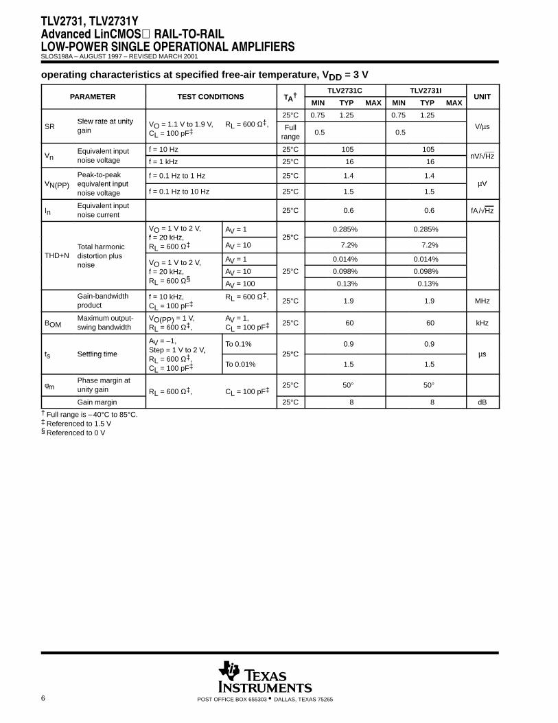
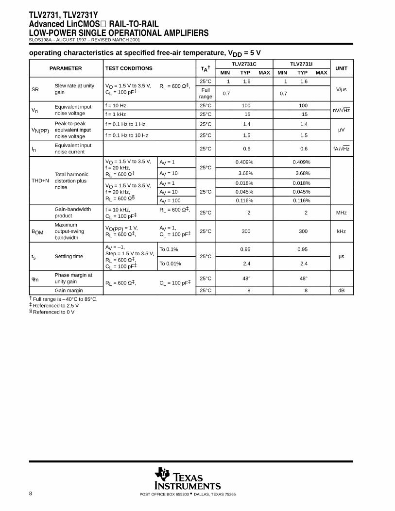
operating characteristics at specified free-air temperature, VDD = 3 V
PARAMETER TEST CONDITIONS TA†TLV2731C TLV2731I
UNITPARAMETER TEST CONDITIONS TA†MIN TYP MAX MIN TYP MAX
UNIT
Slew rate at unity ‡25°C 0.75 1.25 0.75 1.25
SRSlew rate at unitygain
VO = 1.1 V to 1.9 V,CL = 100 pF‡
RL = 600 Ω‡, Fullrange
0.5 0.5V/µs
VEquivalent input f = 10 Hz 25°C 105 105
nV/√HzVnq
noise voltage f = 1 kHz 25°C 16 16nV/√Hz
VN(PP)
Peak-to-peakequivalent input
f = 0.1 Hz to 1 Hz 25°C 1.4 1.4µVVN(PP) equivalent input
noise voltage f = 0.1 Hz to 10 Hz 25°C 1.5 1.5µV
InEquivalent inputnoise current
25°C 0.6 0.6 fA /√Hz
VO = 1 V to 2 V,f 20 kHz
AV = 125°C
0.285% 0.285%
Total harmonic f = 20 kHz,RL = 600 Ω‡ AV = 10
25°C7.2% 7.2%
THD+N distortion plusnoise VO = 1 V to 2 V, AV = 1 0.014% 0.014%noise VO = 1 V to 2 V,
f = 20 kHz,§
AV = 10 25°C 0.098% 0.098%RL = 600 Ω§
AV = 100 0.13% 0.13%
Gain-bandwidthproduct
f = 10 kHz, CL = 100 pF‡
RL = 600 Ω‡, 25°C 1.9 1.9 MHz
BOMMaximum output-swing bandwidth
VO(PP) = 1 V, RL = 600 Ω‡,
AV = 1,CL = 100 pF‡ 25°C 60 60 kHz
t Settling time
AV = –1,Step = 1 V to 2 V,
To 0.1%25°C
0.9 0.9µsts Settling time ,
RL = 600 Ω‡,CL = 100 pF‡ To 0.01%
25°C1.5 1.5
µs
φmPhase margin atunity gain RL = 600 Ω‡, CL = 100 pF‡
25°C 50° 50°
Gain marginL , L
25°C 8 8 dB† Full range is –40°C to 85°C.‡ Referenced to 1.5 V§ Referenced to 0 V
TLV2731, TLV2731YAdvanced LinCMOS RAIL-TO-RAIL
LOW-POWER SINGLE OPERATIONAL AMPLIFIERS
SLOS198A – AUGUST 1997 – REVISED MARCH 2001
7POST OFFICE BOX 655303 • DALLAS, TEXAS 75265
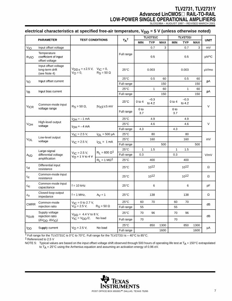
electrical characteristics at specified free-air temperature, VDD = 5 V (unless otherwise noted)
PARAMETER TEST CONDITIONS TA†TLV2731C TLV2731I
UNITPARAMETER TEST CONDITIONS TA†MIN TYP MAX MIN TYP MAX
UNIT
VIO Input offset voltage
V V V
0.7 3 0.7 3 mV
αVIO
Temperaturecoefficient of input
V V V
Full range0 5 0 5 µV/°CαVIO coefficient of input
offset voltage
V V V
0.5 0.5 µV/°C
Input offset voltagelong-term drift(see Note 4)
VDD± = ±2.5 V,VO = 0,
VIC = 0,RS = 50 Ω
25°C 0.003 0.003 µV/mo
IIO Input offset current25°C 0.5 60 0.5 60
pAIIO Input offset currentFull range 150 150
pA
IIB Input bias current25°C 1 60 1 60
pAIIB Input bias currentFull range 150 150
pA
–0 3 –0 325°C 0 to 4
–0.3to 4 2 0 to 4
–0.3to 4 2
VICRCommon-mode input
RS = 50 Ω |VIO| ≤5 mV
25 C 0 to 4 to 4.2 0 to 4 to 4.2VVICR voltage range
RS = 50 Ω, |VIO| ≤5 mV0 to 0 to
Vvoltage range
Full range0 to3 7
0 to3 7Full range 3.7 3.7
Hi h l l t tIOH = –1 mA 25°C 4.9 4.9
VOHHigh-level outputvoltage IOH = 4 mA
25°C 4.6 4.6 Vvoltage IOH = –4 mA
Full range 4.3 4.3
L l l t tVIC = 2.5 V, IOL = 500 µA 25°C 80 80
VOLLow-level outputvoltage VIC = 2 5 V IOL = 1 mA
25°C 160 160 mVvoltage VIC = 2.5 V, IOL = 1 mA
Full range 500 500
Large-signalV 2 5 V R 600 Ω‡
25°C 1 1.5 1 1.5
AVD
Large signaldifferential voltage
VIC = 2.5 V,VO = 1 V to 4 V
RL = 600 Ω‡Full range 0.3 0.3 V/mVVD
amplificationVO = 1 V to 4 V
RL = 1 MΩ‡ 25°C 400 400
ridDifferential inputresistance
25°C 1012 1012 Ω
ricCommon-mode inputresistance
25°C 1012 1012 Ω
cicCommon-mode inputcapacitance
f = 10 kHz 25°C 6 6 pF
zoClosed-loop outputimpedance
f = 1 MHz, AV = 1 25°C 138 138 Ω
CMRRCommon-mode VIC = 0 to 2.7 V, 25°C 60 70 60 70
dBCMRRrejection ratio
IC ,VO = 2.5 V, RS = 50 Ω Full range 55 55
dB
kSVR
Supply voltage rejection ratio
VDD = 4.4 V to 8 V, 25°C 70 96 70 96dBkSVR rejection ratio
(∆VDD /∆VIO)
DD ,VIC = VDD/2, No load Full range 70 70
dB
IDD Supply current VO = 2 5 V No load25°C 850 1300 850 1300
µAIDD Supply current VO = 2.5 V, No loadFull range 1600 1600
µA
† Full range for the TLV2731C is 0°C to 70°C. Full range for the TLV2731I is – 40°C to 85°C.‡ Referenced to 2.5 VNOTE 5: Typical values are based on the input offset voltage shift observed through 500 hours of operating life test at TA = 150°C extrapolated
to TA = 25°C using the Arrhenius equation and assuming an activation energy of 0.96 eV.
TLV2731, TLV2731YAdvanced LinCMOS RAIL-TO-RAILLOW-POWER SINGLE OPERATIONAL AMPLIFIERS
SLOS198A – AUGUST 1997 – REVISED MARCH 2001
8 POST OFFICE BOX 655303 • DALLAS, TEXAS 75265
operating characteristics at specified free-air temperature, VDD = 5 V
PARAMETER TEST CONDITIONS TA†TLV2731C TLV2731I
UNITPARAMETER TEST CONDITIONS TA†MIN TYP MAX MIN TYP MAX
UNIT
Slew rate at unity VO = 1 5 V to 3 5 V R 600 Ω‡25°C 1 1.6 1 1.6
SRSlew rate at unitygain
VO = 1.5 V to 3.5 V,CL = 100 pF‡
RL = 600 Ω‡,Full
range0.7 0.7
V/µs
VEquivalent input f = 10 Hz 25°C 100 100
nV/√HzVnq
noise voltage f = 1 kHz 25°C 15 15nV/√Hz
VN(PP)
Peak-to-peakequivalent input
f = 0.1 Hz to 1 Hz 25°C 1.4 1.4µVVN(PP) equivalent input
noise voltage f = 0.1 Hz to 10 Hz 25°C 1.5 1.5µV
InEquivalent inputnoise current
25°C 0.6 0.6 fA /√Hz
VO = 1.5 V to 3.5 V,f 20 kHz
AV = 125°C
0.409% 0.409%
Total harmonic f = 20 kHz,RL = 600 Ω‡ AV = 10
25°C3.68% 3.68%
THD+N distortion plusnoise VO = 1.5 V to 3.5 V, AV = 1 0.018% 0.018%noise VO = 1.5 V to 3.5 V,
f = 20 kHz,§
AV = 10 25°C 0.045% 0.045%RL = 600 Ω§
AV = 100 0.116% 0.116%
Gain-bandwidthproduct
f = 10 kHz, CL = 100 pF‡
RL = 600 Ω‡, 25°C 2 2 MHz
BOM
Maximumoutput-swingbandwidth
VO(PP) = 1 V, RL = 600 Ω‡,
AV = 1,CL = 100 pF‡ 25°C 300 300 kHz
t Settling time
AV = –1,Step = 1.5 V to 3.5 V,
To 0.1%25°C
0.95 0.95µsts Settling time ,
RL = 600 Ω‡,CL = 100 pF‡ To 0.01%
25°C2.4 2.4
µs
φmPhase margin atunity gain RL = 600 Ω‡, CL = 100 pF‡
25°C 48° 48°
Gain marginL , L
25°C 8 8 dB† Full range is –40°C to 85°C.‡ Referenced to 2.5 V§ Referenced to 0 V
TLV2731, TLV2731YAdvanced LinCMOS RAIL-TO-RAIL
LOW-POWER SINGLE OPERATIONAL AMPLIFIERS
SLOS198A – AUGUST 1997 – REVISED MARCH 2001
9POST OFFICE BOX 655303 • DALLAS, TEXAS 75265
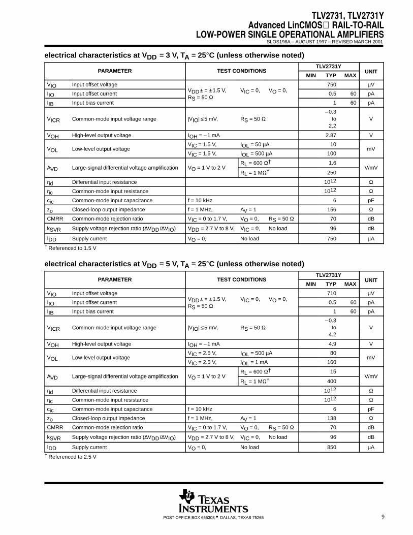
electrical characteristics at VDD = 3 V, TA = 25°C (unless otherwise noted)
PARAMETER TEST CONDITIONSTLV2731Y
UNITPARAMETER TEST CONDITIONSMIN TYP MAX
UNIT
VIO Input offset voltageV ± ±1 5 V V 0 V 0
750 µV
IIO Input offset currentVDD± = ±1.5 V,RS = 50 Ω
VIC = 0, VO = 0,0.5 60 pA
IIB Input bias currentRS = 50 Ω
1 60 pA
–0.3VICR Common-mode input voltage range |VIO| ≤5 mV, RS = 50 Ω to VICR g g IO S
2.2
VOH High-level output voltage IOH = –1 mA 2.87 V
VOL Low level output voltageVIC = 1.5 V, IOL = 50 µA 10
mVVOL Low-level output voltageVIC = 1.5 V, IOL = 500 µA 100
mV
AVD Large signal differential voltage amplification VO = 1 V to 2 VRL = 600 Ω† 1.6
V/mVAVD Large-signal differential voltage amplification VO = 1 V to 2 VRL = 1 Mن 250
V/mV
rid Differential input resistance 1012 Ω
ric Common-mode input resistance 1012 Ω
cic Common-mode input capacitance f = 10 kHz 6 pF
zo Closed-loop output impedance f = 1 MHz, AV = 1 156 Ω
CMRR Common-mode rejection ratio VIC = 0 to 1.7 V, VO = 0, RS = 50 Ω 70 dB
kSVR Supply voltage rejection ratio (∆VDD/∆VIO) VDD 2 7 V to 8 V VIC 0 No load 96 dBkSVR Supply voltage rejection ratio (∆VDD/∆VIO) VDD = 2.7 V to 8 V, VIC = 0, No load 96 dB
IDD Supply current VO = 0, No load 750 µA
† Referenced to 1.5 V
electrical characteristics at VDD = 5 V, TA = 25°C (unless otherwise noted)
PARAMETER TEST CONDITIONSTLV2731Y
UNITPARAMETER TEST CONDITIONSMIN TYP MAX
UNIT
VIO Input offset voltageV ± ±1 5 V V 0 V 0
710 µV
IIO Input offset currentVDD± = ±1.5 V,RS = 50 Ω
VIC = 0, VO = 0,0.5 60 pA
IIB Input bias currentRS = 50 Ω
1 60 pA
–0.3VICR Common-mode input voltage range |VIO| ≤5 mV, RS = 50 Ω to VICR g g IO S
4.2
VOH High-level output voltage IOH = –1 mA 4.9 V
VOL Low level output voltageVIC = 2.5 V, IOL = 500 µA 80
mVVOL Low-level output voltageVIC = 2.5 V, IOL = 1 mA 160
mV
AVD Large signal differential voltage amplification VO = 1 V to 2 VRL = 600 Ω† 15
V/mVAVD Large-signal differential voltage amplification VO = 1 V to 2 VRL = 1 Mن 400
V/mV
rid Differential input resistance 1012 Ω
ric Common-mode input resistance 1012 Ω
cic Common-mode input capacitance f = 10 kHz 6 pF
zo Closed-loop output impedance f = 1 MHz, AV = 1 138 Ω
CMRR Common-mode rejection ratio VIC = 0 to 1.7 V, VO = 0, RS = 50 Ω 70 dB
kSVR Supply voltage rejection ratio (∆VDD/∆VIO) VDD 2 7 V to 8 V VIC 0 No load 96 dBkSVR Supply voltage rejection ratio (∆VDD/∆VIO) VDD = 2.7 V to 8 V, VIC = 0, No load 96 dB
IDD Supply current VO = 0, No load 850 µA
† Referenced to 2.5 V
TLV2731, TLV2731YAdvanced LinCMOS RAIL-TO-RAILLOW-POWER SINGLE OPERATIONAL AMPLIFIERS
SLOS198A – AUGUST 1997 – REVISED MARCH 2001
10 POST OFFICE BOX 655303 • DALLAS, TEXAS 75265
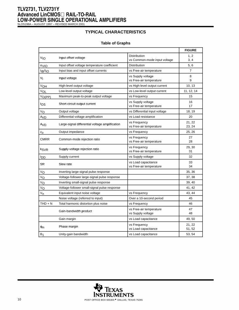
TYPICAL CHARACTERISTICS
Table of Graphs
FIGURE
VIO Input offset voltageDistribution 1, 2
VIO Input offset voltagevs Common-mode input voltage
,3, 4
αVIO Input offset voltage temperature coefficient Distribution 5, 6
IIB/IIO Input bias and input offset currents vs Free-air temperature 7
VI Input voltagevs Supply voltage 8
VI Input voltagey g
vs Free-air temperature 9
VOH High-level output voltage vs High-level output current 10, 13
VOL Low-level output voltage vs Low-level output current 11, 12, 14
VO(PP) Maximum peak-to-peak output voltage vs Frequency 15
IOS Short circuit output currentvs Supply voltage 16
IOS Short-circuit output currenty g
vs Free-air temperature 17
VO Output voltage vs Differential input voltage 18, 19
AVD Differential voltage amplification vs Load resistance 20
AVD Large signal differential voltage amplificationvs Frequency 21, 22
AVD Large-signal differential voltage amplificationq y
vs Free-air temperature,
23, 24
zo Output impedance vs Frequency 25, 26
CMRR Common mode rejection ratiovs Frequency 27
CMRR Common-mode rejection ratioq y
vs Free-air temperature 28
kSVR Supply voltage rejection ratiovs Frequency 29, 30
kSVR Supply-voltage rejection ratioq y
vs Free-air temperature,
31
IDD Supply current vs Supply voltage 32
SR Slew ratevs Load capacitance 33
SR Slew ratevs Free-air temperature 34
VO Inverting large-signal pulse response 35, 36
VO Voltage-follower large-signal pulse response 37, 38
VO Inverting small-signal pulse response 39, 40
VO Voltage-follower small-signal pulse response 41, 42
Vn Equivalent input noise voltage vs Frequency 43, 44
Noise voltage (referred to input) Over a 10-second period 45
THD + N Total harmonic distortion plus noise vs Frequency 46
Gain bandwidth productvs Free-air temperature 47
Gain-bandwidth productvs Supply voltage 48
Gain margin vs Load capacitance 49, 50
φ Phase marginvs Frequency 21, 22φm Phase margin
q yvs Load capacitance
,51, 52
B1 Unity-gain bandwidth vs Load capacitance 53, 54
TLV2731, TLV2731YAdvanced LinCMOS RAIL-TO-RAIL
LOW-POWER SINGLE OPERATIONAL AMPLIFIERS
SLOS198A – AUGUST 1997 – REVISED MARCH 2001
11POST OFFICE BOX 655303 • DALLAS, TEXAS 75265
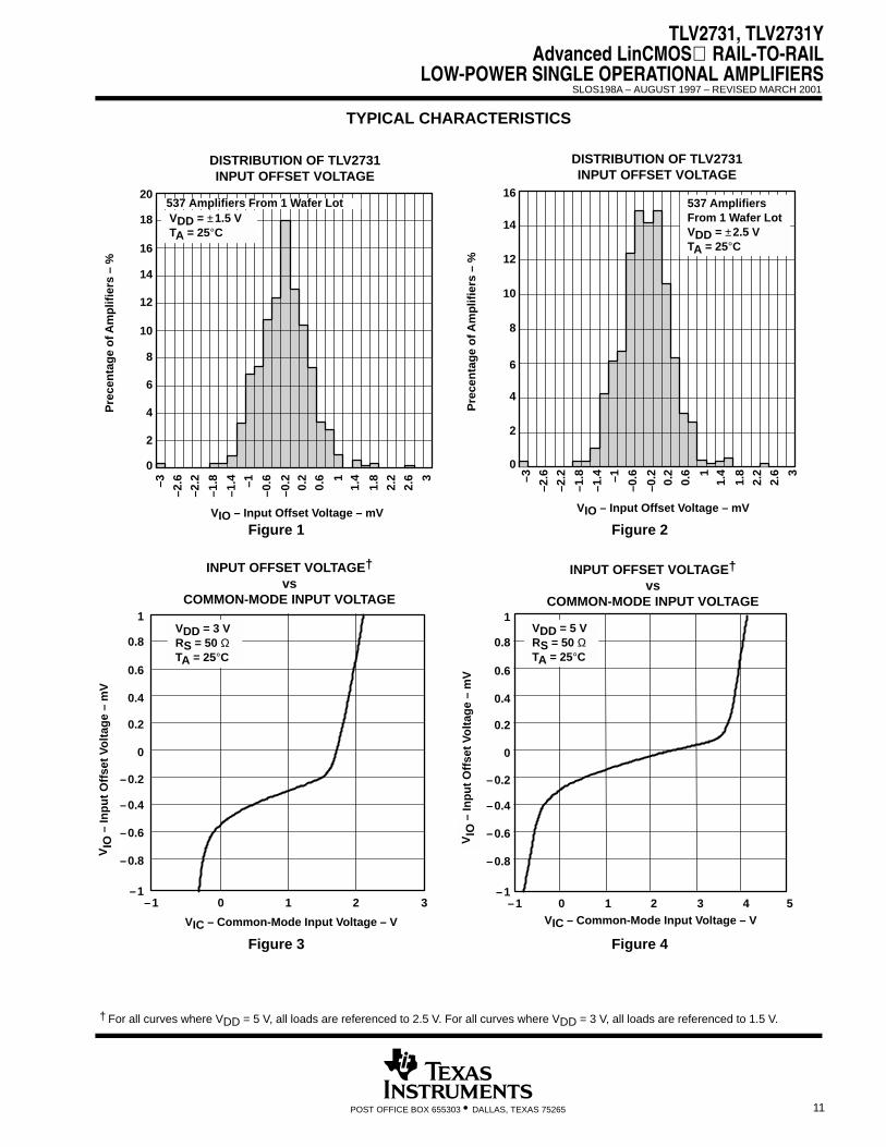
TYPICAL CHARACTERISTICS
Figure 1
10
8
4
0
14
18
20
16
12
6
2
–3
–2.6
–2.2
–1.8
–1.4 –1
–0.6
–0.2 0.2
0.6 1
1.4
1.8
2.2
2.6 3
Pre
cen
tag
e o
f Am
plif
iers
– %
DISTRIBUTION OF TLV2731INPUT OFFSET VOLTAGE
VIO – Input Offset Voltage – mV
VDD = ±1.5 VTA = 25°C
537 Amplifiers From 1 Wafer Lot
Figure 2
8
6
4
0
12
14
16
–3
–2.6
–2.2
–1.8
–1.4 –1
–0.6
–0.2 0.2
0.6 1
1.4
1.8
2.2
2.6 3
VIO – Input Offset Voltage – mV
10
2
Pre
cen
tag
e o
f Am
plif
iers
– %
DISTRIBUTION OF TLV2731INPUT OFFSET VOLTAGE
537 AmplifiersFrom 1 Wafer LotVDD = ±2.5 VTA = 25°C
Figure 3
– In
pu
t O
ffse
t V
olt
age
– m
V
INPUT OFFSET VOLTAGE†
vsCOMMON-MODE INPUT VOLTAGE
ÁÁÁÁ
VIO
VIC – Common-Mode Input Voltage – V
1
0.8
0.6
0.4
0.2
0
–0.2
–0.4
–0.6
–0.8
–1–1 0 1 2
VDD = 3 VRS = 50 ΩTA = 25°C
3
Figure 4
– In
pu
t O
ffse
t V
olt
age
– m
V
INPUT OFFSET VOLTAGE†
vsCOMMON-MODE INPUT VOLTAGE
ÁÁÁÁÁÁ
VIO
VIC – Common-Mode Input Voltage – V
1
0.8
0.6
0.4
0.2
0
–0.2
–0.4
–0.6
–0.8
–1–1 0 1 2 3 4 5
VDD = 5 VRS = 50 ΩTA = 25°C
† For all curves where VDD = 5 V, all loads are referenced to 2.5 V. For all curves where VDD = 3 V, all loads are referenced to 1.5 V.
TLV2731, TLV2731YAdvanced LinCMOS RAIL-TO-RAILLOW-POWER SINGLE OPERATIONAL AMPLIFIERS
SLOS198A – AUGUST 1997 – REVISED MARCH 2001
12 POST OFFICE BOX 655303 • DALLAS, TEXAS 75265
TYPICAL CHARACTERISTICS
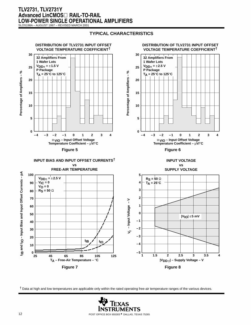
Figure 5
DISTRIBUTION OF TLV2731 INPUT OFFSETVOLTAGE TEMPERATURE COEFFICIENT†
Per
cen
tag
e o
f Am
plif
iers
– %
α VIO – Input Offset VoltageTemperature Coefficient – µV/°C
15
10
5
0
20
25
30
–4 –3 –2 –1 0 1 2 3 4
32 Amplifiers From1 Wafer LotsVDD± = ±1.5 VP PackageTA = 25°C to 125°C
Figure 6
DISTRIBUTION OF TLV2731 INPUT OFFSETVOLTAGE TEMPERATURE COEFFICIENT†
Per
cen
tag
e o
f Am
plif
iers
– %
α VIO – Input Offset VoltageTemperature Coefficient – µV/°C
15
10
5
0
20
25
30
–4 –3 –2 –1 0 1 2 3 4
32 Amplifiers From1 Wafer LotsVDD± = ±2.5 VP PackageTA = 25°C to 125°C
Figure 7
IIB a
nd
IIO
– In
pu
t B
ias
and
Inp
ut
Off
set
Cu
rren
ts –
pA
INPUT BIAS AND INPUT OFFSET CURRENTS†
vsFREE-AIR TEMPERATURE
I IB
I IO
TA – Free-Air Temperature – °C
100
90
80
70
60
50
40
30
20
10
025 45 65 85 105 125
VDD± = ±2.5 VVIC = 0VO = 0RS = 50 Ω
IIB IIO
Figure 8
0
4
1 1.5 2 2.5
– In
pu
t V
olt
age
– V
2
1
3
INPUT VOLTAGEvs
SUPPLY VOLTAGE5
3 3.5 4
–1
–2
–3
–4
–5
RS = 50 ΩTA = 25°C
|VIO| ≤5 mV
ÁÁÁÁ
VI
|VDD±| – Supply Voltage – V
† Data at high and low temperatures are applicable only within the rated operating free-air temperature ranges of the various devices.
TLV2731, TLV2731YAdvanced LinCMOS RAIL-TO-RAIL
LOW-POWER SINGLE OPERATIONAL AMPLIFIERS
SLOS198A – AUGUST 1997 – REVISED MARCH 2001
13POST OFFICE BOX 655303 • DALLAS, TEXAS 75265
TYPICAL CHARACTERISTICS
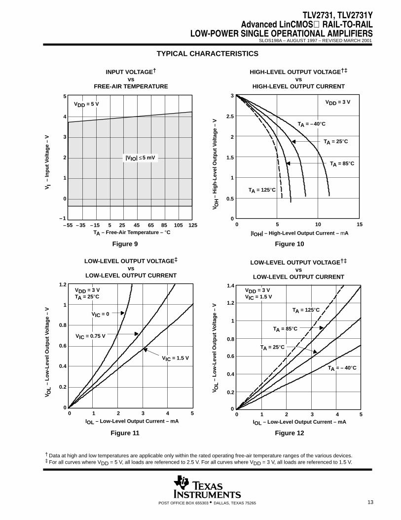
Figure 9
– In
pu
t V
olt
age
– V
INPUT VOLTAGE†
vsFREE-AIR TEMPERATURE
ÁÁVI
TA – Free-Air Temperature – °C
2
1
0
3
4
5
–1–55 –35 –15 5 25 45 65 85
|VIO| ≤5 mV
VDD = 5 V
105 125
Figure 10
– H
igh
-Lev
el O
utp
ut
Vo
ltag
e –
V
HIGH-LEVEL OUTPUT VOLTAGE†‡
vsHIGH-LEVEL OUTPUT CURRENT
ÁÁÁÁV O
H
|IOH| – High-Level Output Current – mA
2
1.5
1
00
2.5
3VDD = 3 V
TA = –40°C
TA = 25°C
TA = 85°C
0.5
TA = 125°C
5 10 15
Figure 11
0.6
0.4
0.2
00 1 2 3
– L
ow
-Lev
el O
utp
ut
Vo
ltag
e –
V
0.8
1
LOW-LEVEL OUTPUT VOLTAGE‡
vsLOW-LEVEL OUTPUT CURRENT
1.2
4 5
ÁÁÁÁ
V OL
IOL – Low-Level Output Current – mA
VDD = 3 VTA = 25°C
VIC = 0
VIC = 0.75 V
VIC = 1.5 V
Figure 12
– L
ow
-Lev
el O
utp
ut
Vo
ltag
e –
V
LOW-LEVEL OUTPUT VOLTAGE†‡
vsLOW-LEVEL OUTPUT CURRENT
ÁÁÁÁÁÁ
V OL
IOL – Low-Level Output Current – mA
0.4
0.2
1.2
00 1 2 3
0.8
0.6
1
1.4
4 5
TA = 85°C
TA = 25°C
TA = 125°C
VDD = 3 VVIC = 1.5 V
TA = – 40°C
† Data at high and low temperatures are applicable only within the rated operating free-air temperature ranges of the various devices.‡ For all curves where VDD = 5 V, all loads are referenced to 2.5 V. For all curves where VDD = 3 V, all loads are referenced to 1.5 V.
TLV2731, TLV2731YAdvanced LinCMOS RAIL-TO-RAILLOW-POWER SINGLE OPERATIONAL AMPLIFIERS
SLOS198A – AUGUST 1997 – REVISED MARCH 2001
14 POST OFFICE BOX 655303 • DALLAS, TEXAS 75265
TYPICAL CHARACTERISTICS
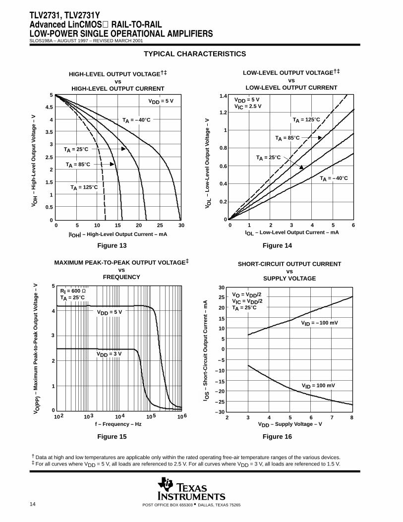
Figure 13
– H
igh
-Lev
el O
utp
ut
Vo
ltag
e –
V
HIGH-LEVEL OUTPUT VOLTAGE†‡
vsHIGH-LEVEL OUTPUT CURRENT
ÁÁÁÁ
V OH
|IOH| – High-Level Output Current – mA
0
VDD = 5 V
TA = –40°C
TA = 25°C
TA = 85°C
TA = 125°C
5
4.5
4
3.5
3
2.5
2
1.5
1
0.5
05 10 15 20 25 30
Figure 14
– L
ow
-Lev
el O
utp
ut
Vo
ltag
e –
V
LOW-LEVEL OUTPUT VOLTAGE†‡
vsLOW-LEVEL OUTPUT CURRENT
ÁÁÁÁV
OL
IOL – Low-Level Output Current – mA
0.6
0.4
0.2
00 1 2 3
1
1.2
1.4
4 5 6
0.8
VDD = 5 VVIC = 2.5 V
TA = –40°C
TA = 85°C
TA = 25°C
TA = 125°C
Figure 15
– M
axim
um
Pea
k-to
-Pea
k O
utp
ut
Vo
ltag
e –
V
f – Frequency – Hz
MAXIMUM PEAK-TO-PEAK OUTPUT VOLTAGE‡
vsFREQUENCY
ÁÁÁÁÁÁ
VO
(PP
)
4
2
1
5
3
0102 103 104 106105
RI = 600 ΩTA = 25°C
VDD = 5 V
VDD = 3 V
Figure 16
– S
ho
rt-C
ircu
it O
utp
ut
Cu
rren
t –
mA
SHORT-CIRCUIT OUTPUT CURRENTvs
SUPPLY VOLTAGE
I OS
VDD – Supply Voltage – V
30
25
20
15
10
5
0
–5
–10
–15
–20
–25
–302 3 4 5 6 7 8
VID = –100 mV
VID = 100 mV
VO = VDD/2VIC = VDD/2TA = 25°C
† Data at high and low temperatures are applicable only within the rated operating free-air temperature ranges of the various devices.‡ For all curves where VDD = 5 V, all loads are referenced to 2.5 V. For all curves where VDD = 3 V, all loads are referenced to 1.5 V.
TLV2731, TLV2731YAdvanced LinCMOS RAIL-TO-RAIL
LOW-POWER SINGLE OPERATIONAL AMPLIFIERS
SLOS198A – AUGUST 1997 – REVISED MARCH 2001
15POST OFFICE BOX 655303 • DALLAS, TEXAS 75265
TYPICAL CHARACTERISTICS
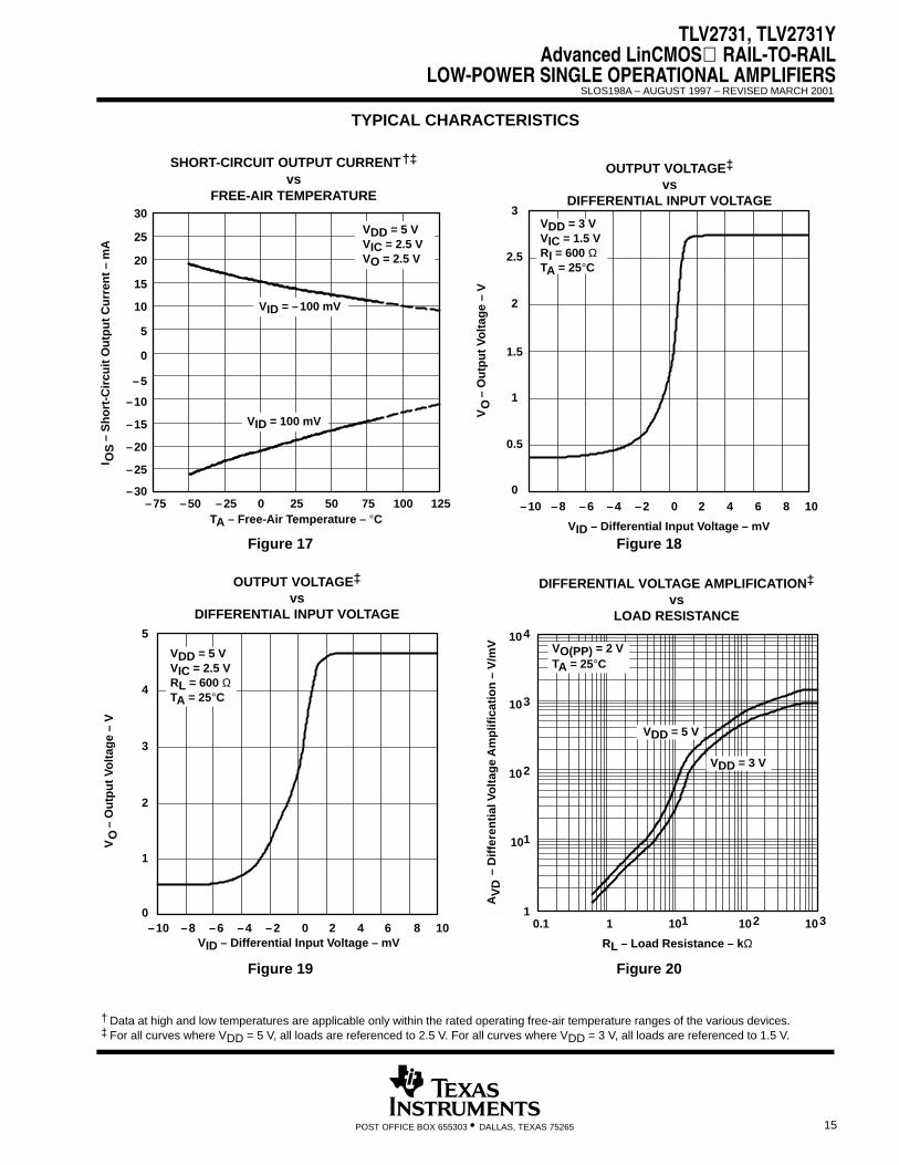
Figure 17
– S
ho
rt-C
ircu
it O
utp
ut
Cu
rren
t –
mA
SHORT-CIRCUIT OUTPUT CURRENT†‡
vsFREE-AIR TEMPERATURE
I OS
TA – Free-Air Temperature – °C–75
30VDD = 5 VVIC = 2.5 VVO = 2.5 V
VID = –100 mV
VID = 100 mV
25
20
15
5
0
–5
–10
–15
–20
–25
10
–30–50 –25 0 25 50 75 100 125
Figure 18
OUTPUT VOLTAGE‡
vsDIFFERENTIAL INPUT VOLTAGE
VID – Differential Input Voltage – mV
010
VDD = 3 VVIC = 1.5 VRI = 600 ΩTA = 25°C
86420–2–4–6–8–10
0.5
1
1.5
2
2.5
3
– O
utp
ut
Vo
ltag
e –
VV
O
Figure 19
OUTPUT VOLTAGE‡
vsDIFFERENTIAL INPUT VOLTAGE
VID – Differential Input Voltage – mV
– O
utp
ut
Vo
ltag
e –
VV
O
01086420–2–4–6–8–10
1
2
3
4
5
VDD = 5 VVIC = 2.5 VRL = 600 ΩTA = 25°C
Figure 20
DIFFERENTIAL VOLTAGE AMPLIFICATION‡
vsLOAD RESISTANCE
RL – Load Resistance – kΩ
– D
iffe
ren
tial
Vo
ltag
e A
mp
lific
atio
n –
V/m
V
ÁÁÁÁÁÁ
AV
D
VO(PP) = 2 VTA = 25°C
VDD = 5 V
VDD = 3 V
0.1 101 102 103
102
101
1
103
104
1
† Data at high and low temperatures are applicable only within the rated operating free-air temperature ranges of the various devices.‡ For all curves where VDD = 5 V, all loads are referenced to 2.5 V. For all curves where VDD = 3 V, all loads are referenced to 1.5 V.
TLV2731, TLV2731YAdvanced LinCMOS RAIL-TO-RAILLOW-POWER SINGLE OPERATIONAL AMPLIFIERS
SLOS198A – AUGUST 1997 – REVISED MARCH 2001
16 POST OFFICE BOX 655303 • DALLAS, TEXAS 75265
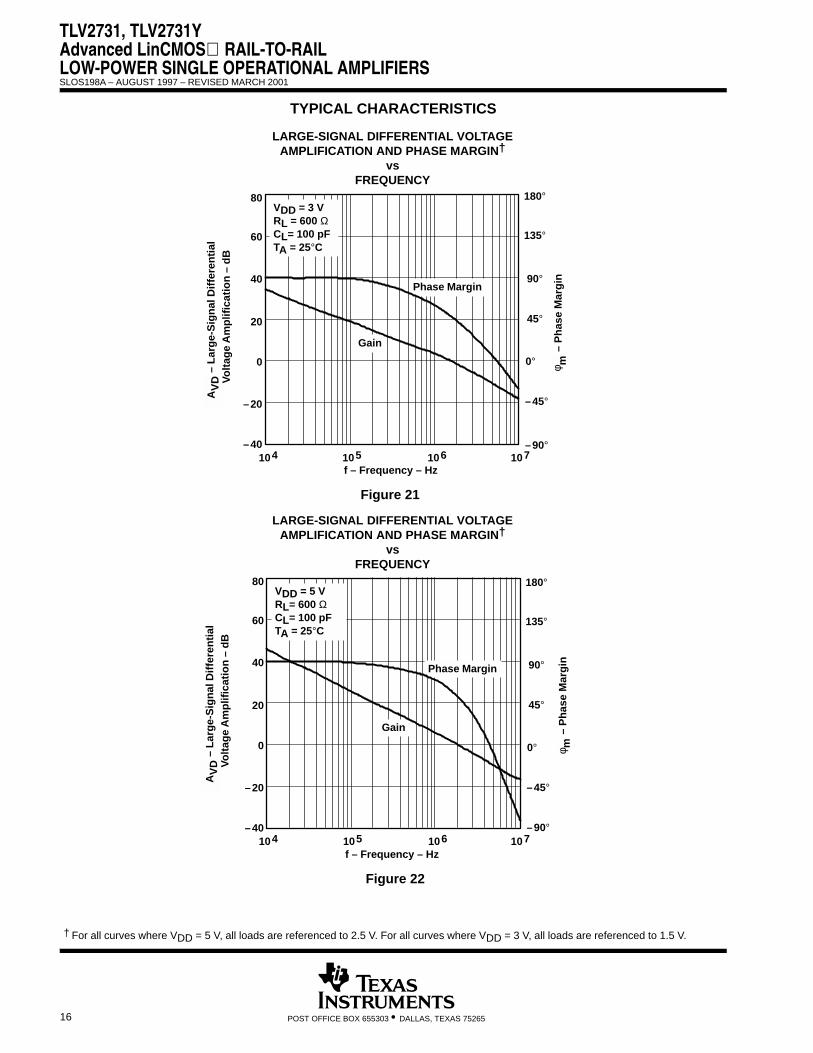
TYPICAL CHARACTERISTICS
om
– P
has
e M
arg
in
φ m
f – Frequency – Hz
LARGE-SIGNAL DIFFERENTIAL VOLTAGEAMPLIFICATION AND PHASE MARGIN†
vsFREQUENCY
AV
D –
Lar
ge-
Sig
nal
Dif
fere
nti
al
ÁÁÁÁA
VD V
olt
age
Am
plif
icat
ion
– d
B
20
80
60
40
0
–20
–40104 105 106 107
180°
135°
90°
45°
0°
–45°
–90°
Gain
VDD = 3 VRL = 600 ΩCL= 100 pFTA = 25°C
Phase Margin
Figure 21
om
– P
has
e M
arg
in
φ m
f – Frequency – Hz
LARGE-SIGNAL DIFFERENTIAL VOLTAGEAMPLIFICATION AND PHASE MARGIN†
vsFREQUENCY
AV
D –
Lar
ge-
Sig
nal
Dif
fere
nti
al
ÁÁÁÁ
AV
D Vo
ltag
e A
mp
lific
atio
n –
dB
20
80
60
40
0
–20
–40104 105 106 107
180°
135°
90°
45°
0°
–45°
–90°
VDD = 5 VRL= 600 ΩCL= 100 pFTA = 25°C
Phase Margin
Gain
Figure 22
† For all curves where VDD = 5 V, all loads are referenced to 2.5 V. For all curves where VDD = 3 V, all loads are referenced to 1.5 V.
TLV2731, TLV2731YAdvanced LinCMOS RAIL-TO-RAIL
LOW-POWER SINGLE OPERATIONAL AMPLIFIERS
SLOS198A – AUGUST 1997 – REVISED MARCH 2001
17POST OFFICE BOX 655303 • DALLAS, TEXAS 75265
TYPICAL CHARACTERISTICS
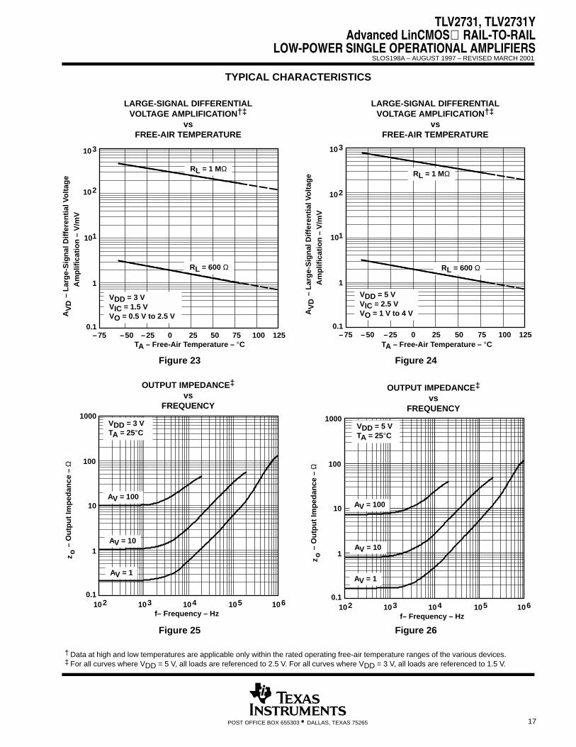
Figure 23
LARGE-SIGNAL DIFFERENTIALVOLTAGE AMPLIFICATION†‡
vsFREE-AIR TEMPERATURE
TA – Free-Air Temperature – °C
– L
arg
e-S
ign
al D
iffe
ren
tial
Vo
ltag
e A
VD
Am
plif
icat
ion
– V
/mV
–50 –25 0 25 50 75 100
RL = 600 Ω
103
102
0.1
VDD = 3 VVIC = 1.5 VVO = 0.5 V to 2.5 V
–75 125
101
1
RL = 1 MΩ
Figure 24
LARGE-SIGNAL DIFFERENTIALVOLTAGE AMPLIFICATION†‡
vsFREE-AIR TEMPERATURE
TA – Free-Air Temperature – °C
– L
arg
e-S
ign
al D
iffe
ren
tial
Vo
ltag
e A
VD
Am
plif
icat
ion
– V
/mV
–50 –25 0 25 50 75 100 125
103
102
0.1–75
VDD = 5 VVIC = 2.5 VVO = 1 V to 4 V
RL = 1 MΩ
RL = 600 Ω
101
1
Figure 25
– O
utp
ut
Imp
edan
ce –
f– Frequency – Hz
OUTPUT IMPEDANCE‡
vsFREQUENCY
Ωz
o
10
1
0.1
1000
100
102 103 104 105 106
AV = 100
AV = 10
AV = 1
VDD = 3 VTA = 25°C
Figure 26
– O
utp
ut
Imp
edan
ce –
f– Frequency – Hz
OUTPUT IMPEDANCE‡
vsFREQUENCY
Ωz
o
10
1
0.1
1000
100
102 103 104 105 106
AV = 100
AV = 10
AV = 1
VDD = 5 VTA = 25°C
† Data at high and low temperatures are applicable only within the rated operating free-air temperature ranges of the various devices.‡ For all curves where VDD = 5 V, all loads are referenced to 2.5 V. For all curves where VDD = 3 V, all loads are referenced to 1.5 V.
TLV2731, TLV2731YAdvanced LinCMOS RAIL-TO-RAILLOW-POWER SINGLE OPERATIONAL AMPLIFIERS
SLOS198A – AUGUST 1997 – REVISED MARCH 2001
18 POST OFFICE BOX 655303 • DALLAS, TEXAS 75265
TYPICAL CHARACTERISTICS
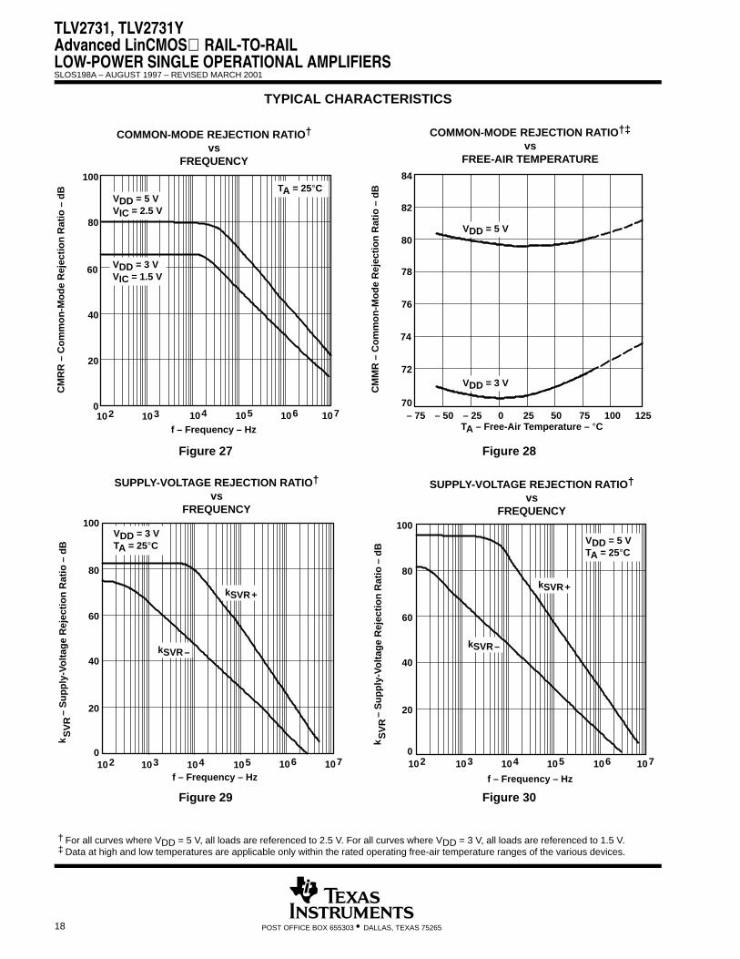
Figure 27
CM
RR
– C
om
mo
n-M
od
e R
ejec
tio
n R
atio
– d
B
f – Frequency – Hz
COMMON-MODE REJECTION RATIO†
vsFREQUENCY
80
40
20
0
100
60
102 103 104 105 106
VDD = 3 VVIC = 1.5 V
107
VDD = 5 VVIC = 2.5 V
TA = 25°C
Figure 28
CM
MR
– C
om
mo
n-M
od
e R
ejec
tio
n R
atio
– d
B
COMMON-MODE REJECTION RATIO†‡
vsFREE-AIR TEMPERATURE
TA – Free-Air Temperature – °C
76
72
70
82
74
80
78
84
– 50 – 25 0 25 50 75 100– 75 125
VDD = 5 V
VDD = 3 V
Figure 29
– S
up
ply
-Vo
ltag
e R
ejec
tio
n R
atio
– d
B
f – Frequency – Hz
SUPPLY-VOLTAGE REJECTION RATIO†
vsFREQUENCY
ÁÁÁ
kS
VR
60
40
20
100
80
0102 103 104 105 106 107
VDD = 3 VTA = 25°C
kSVR+
kSVR–
Figure 30
– S
up
ply
-Vo
ltag
e R
ejec
tio
n R
atio
– d
B
f – Frequency – Hz
SUPPLY-VOLTAGE REJECTION RATIO†
vsFREQUENCY
ÁÁÁÁÁÁ
kS
VR
100
80
60
40
20
0102 103 104 105 106
kSVR–
107
VDD = 5 VTA = 25°C
kSVR+
‡ Data at high and low temperatures are applicable only within the rated operating free-air temperature ranges of the various devices.
† For all curves where VDD = 5 V, all loads are referenced to 2.5 V. For all curves where VDD = 3 V, all loads are referenced to 1.5 V.
TLV2731, TLV2731YAdvanced LinCMOS RAIL-TO-RAIL
LOW-POWER SINGLE OPERATIONAL AMPLIFIERS
SLOS198A – AUGUST 1997 – REVISED MARCH 2001
19POST OFFICE BOX 655303 • DALLAS, TEXAS 75265
TYPICAL CHARACTERISTICS
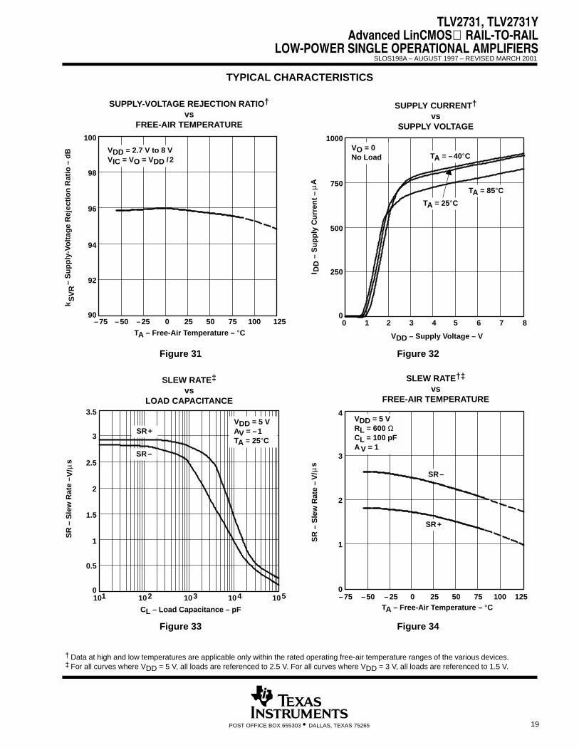
Figure 31
– S
up
ply
-Vo
ltag
e R
ejec
tio
n R
atio
– d
B
SUPPLY-VOLTAGE REJECTION RATIO†
vsFREE-AIR TEMPERATURE
ÁÁÁÁÁÁ
kS
VR
TA – Free-Air Temperature – °C
100
98
96
94
92
90–50 –25 0 25 50 75 100 125–75
VDD = 2.7 V to 8 VVIC = VO = VDD /2
Figure 32
– S
up
ply
Cu
rren
t –
Aµ
ÁÁÁÁÁÁ
I DD
VDD – Supply Voltage – V
SUPPLY CURRENT†
vsSUPPLY VOLTAGE
TA = 25°C
TA = 85°C
VO = 0 No Load
1000
750
500
250
00 1 2 3 4 5 6 7 8
TA = –40°C
Figure 33
SR
– S
lew
Rat
e –
SLEW RATE‡
vsLOAD CAPACITANCE
CL – Load Capacitance – pF
sµ
V/
101 102 103 104 105
VDD = 5 VAV = –1TA = 25°C
SR–
SR+
3.5
3
2.5
2
1.5
1
0.5
0
Figure 34
SR
– S
lew
Rat
e –
SLEW RATE†‡
vsFREE-AIR TEMPERATURE
sµ
V/
TA – Free-Air Temperature – °C–50 –25 0 25 50 75 100–75 125
4
3
2
1
0
SR–
SR+
VDD = 5 VRL = 600 ΩCL = 100 pFAV = 1
† Data at high and low temperatures are applicable only within the rated operating free-air temperature ranges of the various devices.‡ For all curves where VDD = 5 V, all loads are referenced to 2.5 V. For all curves where VDD = 3 V, all loads are referenced to 1.5 V.
TLV2731, TLV2731YAdvanced LinCMOS RAIL-TO-RAILLOW-POWER SINGLE OPERATIONAL AMPLIFIERS
SLOS198A – AUGUST 1997 – REVISED MARCH 2001
20 POST OFFICE BOX 655303 • DALLAS, TEXAS 75265
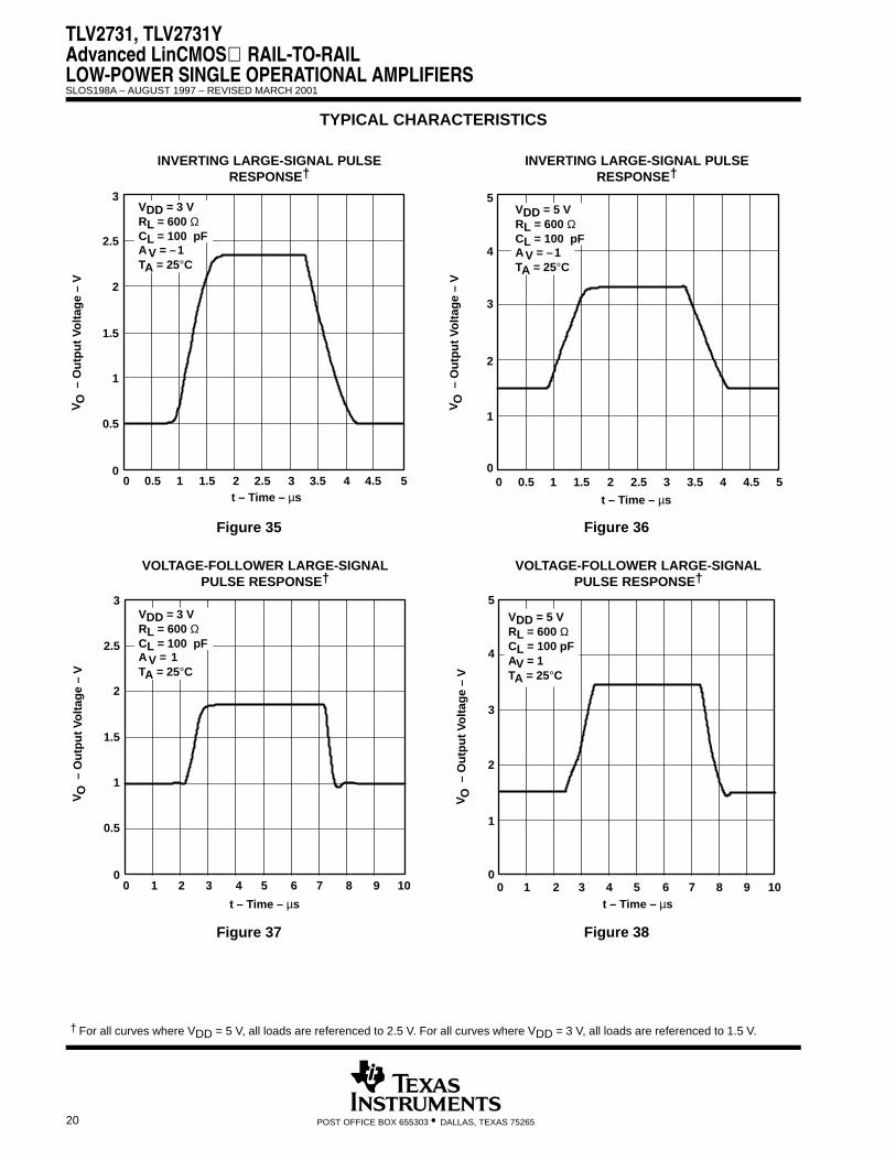
TYPICAL CHARACTERISTICS
Figure 35
– O
utp
ut
Vo
ltag
e –
V
INVERTING LARGE-SIGNAL PULSERESPONSE†
VO
t – Time – µs
1.5
1
0.5
00
2
2.5
3
0.5 1 1.5 2 2.5 3 3.5 4 4.5 5
AV = –1TA = 25°C
VDD = 3 VRL = 600 ΩCL = 100 pF
Figure 36
INVERTING LARGE-SIGNAL PULSERESPONSE†
t – Time – µs
– O
utp
ut
Vo
ltag
e –
VV
O
5
0
4
3
2
1
00.5 1 1.5 2 2.5 3 3.5 4 4.5 5
AV = –1TA = 25°C
VDD = 5 VRL = 600 ΩCL = 100 pF
Figure 37
VOLTAGE-FOLLOWER LARGE-SIGNALPULSE RESPONSE†
– O
utp
ut
Vo
ltag
e –
VV
O
t – Time – µs
1.5
1
0.5
00 1 2 3 4 5 6
2
2.5
3
7 8 9 10
AV = 1TA = 25°C
VDD = 3 VRL = 600 ΩCL = 100 pF
Figure 38
VOLTAGE-FOLLOWER LARGE-SIGNALPULSE RESPONSE†
– O
utp
ut
Vo
ltag
e –
VV
O
t – Time – µs
2
1
00 1 2 3 4 5 6
3
4
5
7 8 9 10
VDD = 5 VRL = 600 ΩCL = 100 pFAV = 1TA = 25°C
† For all curves where VDD = 5 V, all loads are referenced to 2.5 V. For all curves where VDD = 3 V, all loads are referenced to 1.5 V.
TLV2731, TLV2731YAdvanced LinCMOS RAIL-TO-RAIL
LOW-POWER SINGLE OPERATIONAL AMPLIFIERS
SLOS198A – AUGUST 1997 – REVISED MARCH 2001
21POST OFFICE BOX 655303 • DALLAS, TEXAS 75265
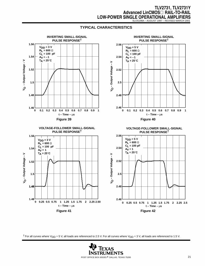
TYPICAL CHARACTERISTICS
Figure 39
INVERTING SMALL-SIGNALPULSE RESPONSE†
– O
utp
ut
Vo
ltag
e –
VV
O
t – Time – µs
0
1.56
1.54
1.52
1.5
1.48
1.460.1 0.2 0.3 0.4 0.5 0.6 0.7 0.8 0.9 1
VDD = 3 VRL = 600 ΩCL = 100 pFAV = –1TA = 25°C
Figure 40
VO
– O
utp
ut
Vo
ltag
e –
V
INVERTING SMALL-SIGNALPULSE RESPONSE†
VO
t – Time – µs
2.5
2.48
2.460
2.52
2.54
2.56
0.1 0.2 0.3 0.4 0.5 0.6 0.7 0.8 0.9 1
VDD = 5 VRL = 600 ΩCL = 100 pFAV = –1TA = 25°C
Figure 41
VOLTAGE-FOLLOWER SMALL-SIGNALPULSE RESPONSE†
VO
– O
utp
ut
Vo
ltag
e –
VV
O
t – Time – µs0
1.56
1.54
1.52
1.5
1.481.48
1.480.25 0.5 0.75 1 1.25 1.5 1.75 2 2.25 2.50
VDD = 3 VRL = 600 ΩCL = 100 pFAV = 1TA = 25°C
Figure 42
VOLTAGE-FOLLOWER SMALL-SIGNALPULSE RESPONSE†
VO
– O
utp
ut
Vo
ltag
e –
VV
O
t – Time – µs0
2.56
2.54
2.52
2.5
2.48
2.460.25 0.5 0.75 1 1.25 1.5 1.75 2 2.25 2.5
VDD = 5 VRL = 600 ΩCL = 100 pFAV = 1TA = 25°C
† For all curves where VDD = 5 V, all loads are referenced to 2.5 V. For all curves where VDD = 3 V, all loads are referenced to 1.5 V.
TLV2731, TLV2731YAdvanced LinCMOS RAIL-TO-RAILLOW-POWER SINGLE OPERATIONAL AMPLIFIERS
SLOS198A – AUGUST 1997 – REVISED MARCH 2001
22 POST OFFICE BOX 655303 • DALLAS, TEXAS 75265
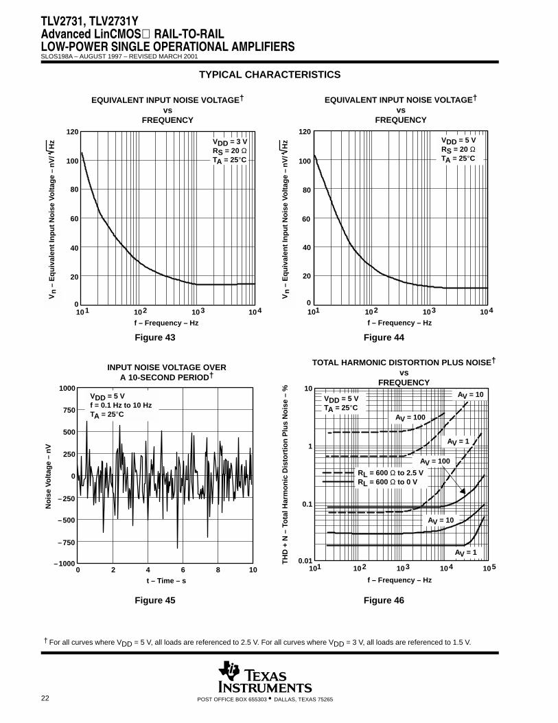
TYPICAL CHARACTERISTICS
Figure 43
– E
qu
ival
ent
Inp
ut
No
ise
Vo
ltag
e –
f – Frequency – Hz
EQUIVALENT INPUT NOISE VOLTAGE†
vsFREQUENCY
Vn
nV
/H
z
80
60
40
0
120
100
20
101 102 103 104
VDD = 3 VRS = 20 ΩTA = 25°C
Figure 44
– E
qu
ival
ent
Inp
ut
No
ise
Vo
ltag
e –
f – Frequency – Hz
EQUIVALENT INPUT NOISE VOLTAGE†
vsFREQUENCY
Vn
nV
/H
z
80
40
20
0
120
60
100
101 102 103 104
VDD = 5 VRS = 20 ΩTA = 25°C
Figure 45
No
ise
Vo
ltag
e –
nV
t – Time – s
INPUT NOISE VOLTAGE OVERA 10-SECOND PERIOD†
0 2 4 6
0
750
1000
8 10
500
–250
–500
–750
–1000
250
VDD = 5 Vf = 0.1 Hz to 10 HzTA = 25°C
Figure 46
TH
D +
N –
To
tal H
arm
on
ic D
isto
rtio
n P
lus
No
ise
– %
f – Frequency – Hz
TOTAL HARMONIC DISTORTION PLUS NOISE†
vsFREQUENCY
0.1
10
0.01101 102 103 104 105
1
AV = 100
AV = 10
AV = 1
AV = 100
AV = 10
AV = 1
VDD = 5 VTA = 25°C
RL = 600 Ω to 2.5 VRL = 600 Ω to 0 V
† For all curves where VDD = 5 V, all loads are referenced to 2.5 V. For all curves where VDD = 3 V, all loads are referenced to 1.5 V.
TLV2731, TLV2731YAdvanced LinCMOS RAIL-TO-RAIL
LOW-POWER SINGLE OPERATIONAL AMPLIFIERS
SLOS198A – AUGUST 1997 – REVISED MARCH 2001
23POST OFFICE BOX 655303 • DALLAS, TEXAS 75265
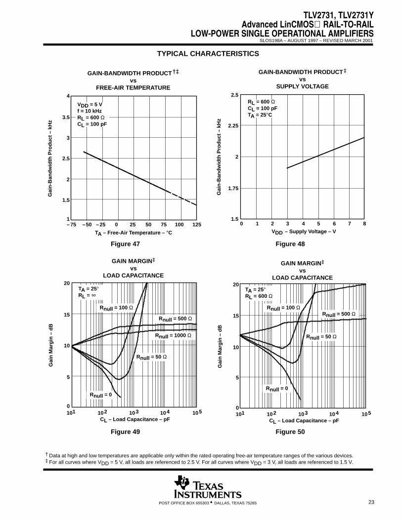
TYPICAL CHARACTERISTICS
Figure 47
Gai
n-B
and
wid
th P
rod
uct
– k
Hz
GAIN-BANDWIDTH PRODUCT†‡
vsFREE-AIR TEMPERATURE
TA – Free-Air Temperature – °C
4
–50 –25 0 25 50 10075 125–75
3.5
3
2.5
2
1.5
1
VDD = 5 Vf = 10 kHzRL = 600 ΩCL = 100 pF
Figure 48
Gai
n-B
and
wid
th P
rod
uct
– k
Hz
GAIN-BANDWIDTH PRODUCT‡
vsSUPPLY VOLTAGE
VDD – Supply Voltage – V
0 2 3 5
2.5
7 81 4 6
2.25
2
1.75
1.5
RL = 600 ΩCL = 100 pFTA = 25°C
Figure 49
Gai
n M
arg
in –
dB
GAIN MARGIN‡
vsLOAD CAPACITANCE
CL – Load Capacitance – pF
20
10
5
0
15
101 102 103 105104
Rnull = 0
Rnull = 50 Ω
Rnull = 100 Ω
Rnull = 500 Ω
Rnull = 1000 Ω
TA = 25°RL = ∞
Figure 50
Gai
n M
arg
in –
dB
GAIN MARGIN‡
vsLOAD CAPACITANCE
CL – Load Capacitance – pF
20
101 102 103 105104
Rnull = 50 Ω
Rnull = 100 Ω
TA = 25°RL = 600 Ω
Rnull = 0
Rnull = 500 Ω15
10
5
0
† Data at high and low temperatures are applicable only within the rated operating free-air temperature ranges of the various devices.‡ For all curves where VDD = 5 V, all loads are referenced to 2.5 V. For all curves where VDD = 3 V, all loads are referenced to 1.5 V.
TLV2731, TLV2731YAdvanced LinCMOS RAIL-TO-RAILLOW-POWER SINGLE OPERATIONAL AMPLIFIERS
SLOS198A – AUGUST 1997 – REVISED MARCH 2001
24 POST OFFICE BOX 655303 • DALLAS, TEXAS 75265
TYPICAL CHARACTERISTICS
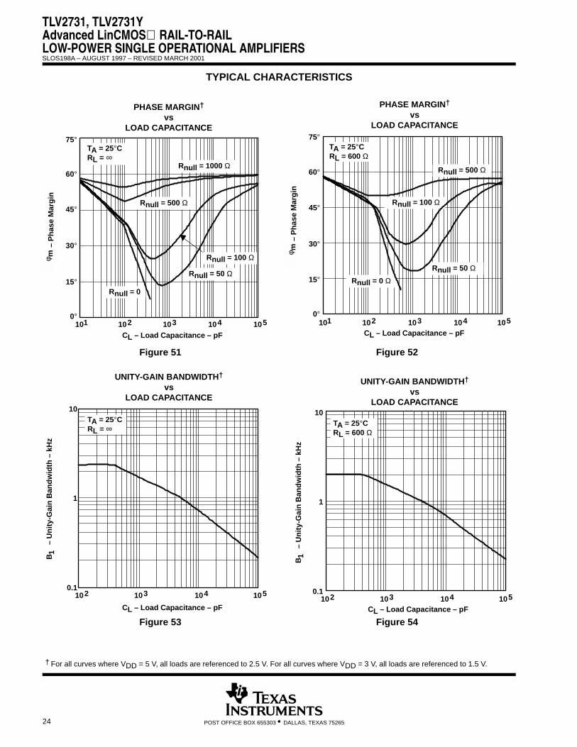
Figure 51
om
– P
has
e M
arg
in
PHASE MARGIN†
vsLOAD CAPACITANCE
CL – Load Capacitance – pF
mφ
101 102 103 105
75°
60°
45°
30°
15°
0°
Rnull = 50 Ω
Rnull = 100 Ω
Rnull = 500 Ω
Rnull = 1000 Ω
TA = 25°CRL = ∞
104
Rnull = 0
Figure 52
Rnull = 50 Ω
Rnull = 100 Ω
Rnull = 0 Ω
Rnull = 500 Ω
TA = 25°CRL = 600 Ω
PHASE MARGIN†
vsLOAD CAPACITANCE
CL – Load Capacitance – pF101 102 103 104 105
75°
60°
45°
30°
15°
0°
om
– P
has
e M
arg
inmφ
Figure 53
TA = 25°CRL = ∞
– U
nit
y-G
ain
Ban
dw
idth
– k
Hz
UNITY-GAIN BANDWIDTH†
vsLOAD CAPACITANCE
ÁÁÁÁB
1
10
105103 104
CL – Load Capacitance – pF
1
0.1102
Figure 54
TA = 25°CRL = 600 Ω
– U
nit
y-G
ain
Ban
dw
idth
– k
Hz
UNITY-GAIN BANDWIDTH†
vsLOAD CAPACITANCE
ÁÁÁÁ
B1
10
105103 104
CL – Load Capacitance – pF
1
0.1102
† For all curves where VDD = 5 V, all loads are referenced to 2.5 V. For all curves where VDD = 3 V, all loads are referenced to 1.5 V.
TLV2731, TLV2731YAdvanced LinCMOS RAIL-TO-RAIL
LOW-POWER SINGLE OPERATIONAL AMPLIFIERS
SLOS198A – AUGUST 1997 – REVISED MARCH 2001
25POST OFFICE BOX 655303 • DALLAS, TEXAS 75265
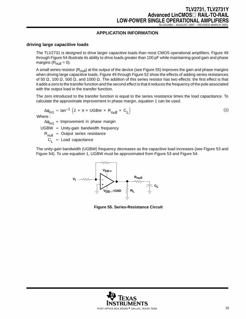
APPLICATION INFORMATION
driving large capacitive loads
The TLV2731 is designed to drive larger capacitive loads than most CMOS operational amplifiers. Figure 49through Figure 54 illustrate its ability to drive loads greater than 100 pF while maintaining good gain and phasemargins (Rnull = 0).
A small series resistor (Rnull) at the output of the device (see Figure 55) improves the gain and phase marginswhen driving large capacitive loads. Figure 49 through Figure 52 show the effects of adding series resistancesof 50 Ω , 100 Ω , 500 Ω , and 1000 Ω . The addition of this series resistor has two effects: the first effect is thatit adds a zero to the transfer function and the second effect is that it reduces the frequency of the pole associatedwith the output load in the transfer function.
The zero introduced to the transfer function is equal to the series resistance times the load capacitance. Tocalculate the approximate improvement in phase margin, equation 1 can be used.
∆φm1 tan–1 2 × π × UGBW × Rnull × CL
∆φm1 Improvement in phase margin
UGBW Unity-gain bandwidth frequencyRnull Output series resistance
CL Load capacitance
(1)
Where :
The unity-gain bandwidth (UGBW) frequency decreases as the capacitive load increases (see Figure 53 andFigure 54). To use equation 1, UGBW must be approximated from Figure 53 and Figure 54.
VDD– /GND
VDD+
Rnull
CL
VI
+
–
RL
Figure 55. Series-Resistance Circuit
TLV2731, TLV2731YAdvanced LinCMOS RAIL-TO-RAILLOW-POWER SINGLE OPERATIONAL AMPLIFIERS
SLOS198A – AUGUST 1997 – REVISED MARCH 2001
26 POST OFFICE BOX 655303 • DALLAS, TEXAS 75265
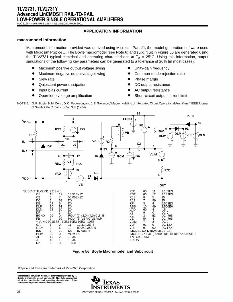
APPLICATION INFORMATION
macromodel information
Macromodel information provided was derived using Microsim Parts , the model generation software usedwith Microsim PSpice . The Boyle macromodel (see Note 6) and subcircuit in Figure 56 are generated usingthe TLV2731 typical electrical and operating characteristics at TA = 25°C. Using this information, outputsimulations of the following key parameters can be generated to a tolerance of 20% (in most cases):
Maximum positive output voltage swing Maximum negative output voltage swing Slew rate Quiescent power dissipation Input bias current Open-loop voltage amplification
Unity-gain frequency Common-mode rejection ratio Phase margin DC output resistance AC output resistance Short-circuit output current limit
NOTE 6: G. R. Boyle, B. M. Cohn, D. O. Pederson, and J. E. Solomon, “Macromodeling of Integrated Circuit Operational Amplifiers,” IEEE Journalof Solid-State Circuits, SC-9, 353 (1974).
OUT
+
–
+
–
+
–
+
–
+–
+
–
+
– +
–
+–
.SUBCKT TLV2731 1 2 3 4 5C1 11 12 13.51E–12C2 6 7 50.00E–12DC 5 53 DXDE 54 5 DXDLP 90 91 DXDLN 92 90 DXDP 4 3 DXEGND 99 0 POLY (2) (3,0) (4,0) 0 .5 .5FB 7 99 POLY (5) VB VC VE VLP+ VLN 0 90.83E3 –10E3 10E3 10E3 –10E3GA 6 0 11 12 314.2E–6GCM 0 6 10 99 242.35E–9ISS 3 10 DC 87.00E–6HLIM 90 0 VLIM 1KJ1 11 2 10 JXJ2 12 1 10 JXR2 6 9 100.0E3
RD1 60 11 3.183E3RD2 60 12 3.183E3R01 8 5 25R02 7 99 25RP 3 4 6.553E3RSS 10 99 2.500E6VAD 60 4 –.5VB 9 0 DC 0VC 3 53 DC .795VE 54 4 DC .795VLIM 7 8 DC 0VLP 91 0 DC 12.4VLN 0 92 DC 17.4.MODEL DX D (IS=800.0E–18).MODEL JX PJF (IS=500.0E–15 BETA=2.939E–3+ VTO=–.065).ENDS
VDD+
RP
IN –2
IN+1
VDD–
VAD
RD1
11
J1 J2
10
RSS ISS
3
12
RD2
60
VE
54DE
DP
VC
DC
4
C1
53
R2
6
9
EGND
VB
FB
C2
GCM GA VLIM
8
5
RO1
RO2
HLIM
90
DLP
91
DLN
92
VLNVLP
99
7
Figure 56. Boyle Macromodel and Subcircuit
PSpice and Parts are trademark of MicroSim Corporation.
Macromodels, simulation models, or other models provided by TI,directly or indirectly, are not warranted by TI as fully representingall of the specification and operating characteristics of thesemiconductor product to which the model relates.
TLV2731, TLV2731YAdvanced LinCMOS RAIL-TO-RAIL
LOW-POWER SINGLE OPERATIONAL AMPLIFIERS
SLOS198A – AUGUST 1997 – REVISED MARCH 2001
27POST OFFICE BOX 655303 • DALLAS, TEXAS 75265
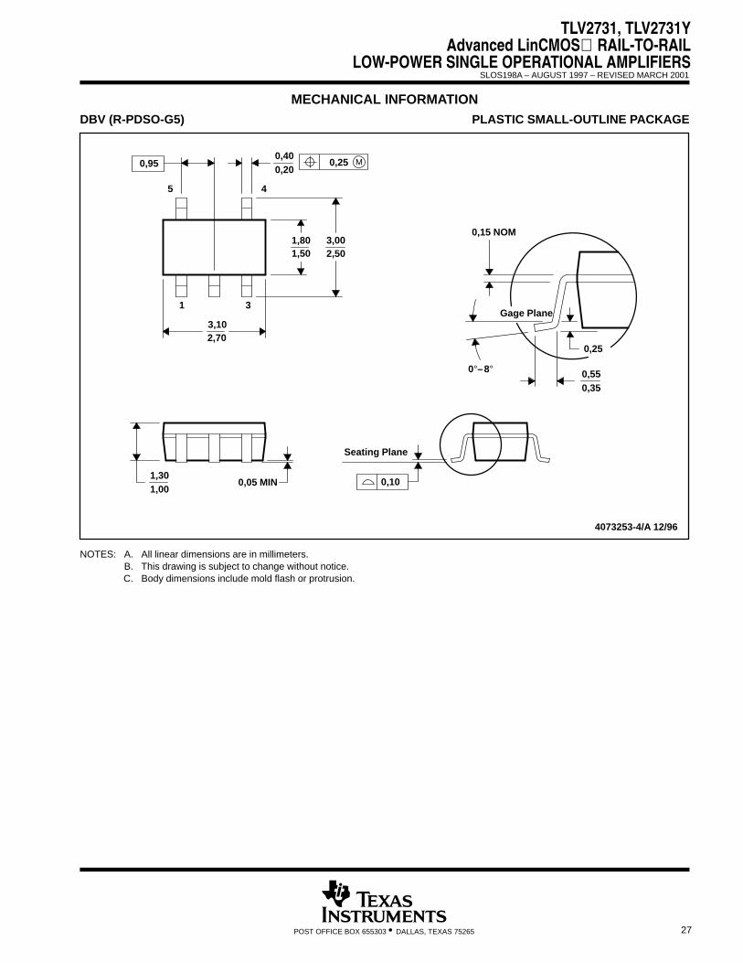
MECHANICAL INFORMATIONDBV (R-PDSO-G5) PLASTIC SMALL-OUTLINE PACKAGE
0,25
0,350,55
Gage Plane
0,15 NOM
4073253-4/A 12/96
2,503,00
0,400,20
1,501,80
45
3
3,10
1
2,70
1,001,30
0,05 MIN
Seating Plane
0,10
0,95 M0,25
0°–8°
NOTES: A. All linear dimensions are in millimeters.B. This drawing is subject to change without notice.C. Body dimensions include mold flash or protrusion.
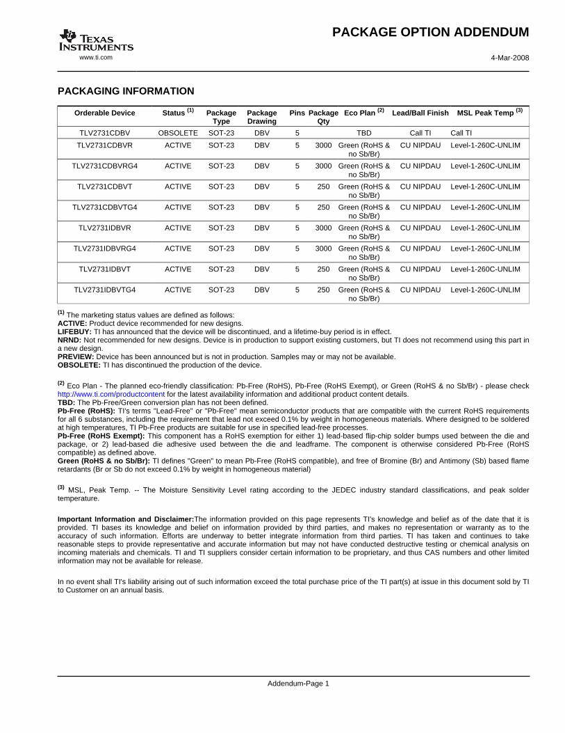
PACKAGING INFORMATION
Orderable Device Status (1) PackageType
PackageDrawing
Pins PackageQty
Eco Plan (2) Lead/Ball Finish MSL Peak Temp (3)
TLV2731CDBV OBSOLETE SOT-23 DBV 5 TBD Call TI Call TI
TLV2731CDBVR ACTIVE SOT-23 DBV 5 3000 Green (RoHS &no Sb/Br)
CU NIPDAU Level-1-260C-UNLIM
TLV2731CDBVRG4 ACTIVE SOT-23 DBV 5 3000 Green (RoHS &no Sb/Br)
CU NIPDAU Level-1-260C-UNLIM
TLV2731CDBVT ACTIVE SOT-23 DBV 5 250 Green (RoHS &no Sb/Br)
CU NIPDAU Level-1-260C-UNLIM
TLV2731CDBVTG4 ACTIVE SOT-23 DBV 5 250 Green (RoHS &no Sb/Br)
CU NIPDAU Level-1-260C-UNLIM
TLV2731IDBVR ACTIVE SOT-23 DBV 5 3000 Green (RoHS &no Sb/Br)
CU NIPDAU Level-1-260C-UNLIM
TLV2731IDBVRG4 ACTIVE SOT-23 DBV 5 3000 Green (RoHS &no Sb/Br)
CU NIPDAU Level-1-260C-UNLIM
TLV2731IDBVT ACTIVE SOT-23 DBV 5 250 Green (RoHS &no Sb/Br)
CU NIPDAU Level-1-260C-UNLIM
TLV2731IDBVTG4 ACTIVE SOT-23 DBV 5 250 Green (RoHS &no Sb/Br)
CU NIPDAU Level-1-260C-UNLIM
(1) The marketing status values are defined as follows:ACTIVE: Product device recommended for new designs.LIFEBUY: TI has announced that the device will be discontinued, and a lifetime-buy period is in effect.NRND: Not recommended for new designs. Device is in production to support existing customers, but TI does not recommend using this part ina new design.PREVIEW: Device has been announced but is not in production. Samples may or may not be available.OBSOLETE: TI has discontinued the production of the device.
(2) Eco Plan - The planned eco-friendly classification: Pb-Free (RoHS), Pb-Free (RoHS Exempt), or Green (RoHS & no Sb/Br) - please checkhttp://www.ti.com/productcontent for the latest availability information and additional product content details.TBD: The Pb-Free/Green conversion plan has not been defined.Pb-Free (RoHS): TI's terms "Lead-Free" or "Pb-Free" mean semiconductor products that are compatible with the current RoHS requirementsfor all 6 substances, including the requirement that lead not exceed 0.1% by weight in homogeneous materials. Where designed to be solderedat high temperatures, TI Pb-Free products are suitable for use in specified lead-free processes.Pb-Free (RoHS Exempt): This component has a RoHS exemption for either 1) lead-based flip-chip solder bumps used between the die andpackage, or 2) lead-based die adhesive used between the die and leadframe. The component is otherwise considered Pb-Free (RoHScompatible) as defined above.Green (RoHS & no Sb/Br): TI defines "Green" to mean Pb-Free (RoHS compatible), and free of Bromine (Br) and Antimony (Sb) based flameretardants (Br or Sb do not exceed 0.1% by weight in homogeneous material)
(3) MSL, Peak Temp. -- The Moisture Sensitivity Level rating according to the JEDEC industry standard classifications, and peak soldertemperature.
Important Information and Disclaimer:The information provided on this page represents TI's knowledge and belief as of the date that it isprovided. TI bases its knowledge and belief on information provided by third parties, and makes no representation or warranty as to theaccuracy of such information. Efforts are underway to better integrate information from third parties. TI has taken and continues to takereasonable steps to provide representative and accurate information but may not have conducted destructive testing or chemical analysis onincoming materials and chemicals. TI and TI suppliers consider certain information to be proprietary, and thus CAS numbers and other limitedinformation may not be available for release.
In no event shall TI's liability arising out of such information exceed the total purchase price of the TI part(s) at issue in this document sold by TIto Customer on an annual basis.
PACKAGE OPTION ADDENDUM
www.ti.com 4-Mar-2008
Addendum-Page 1
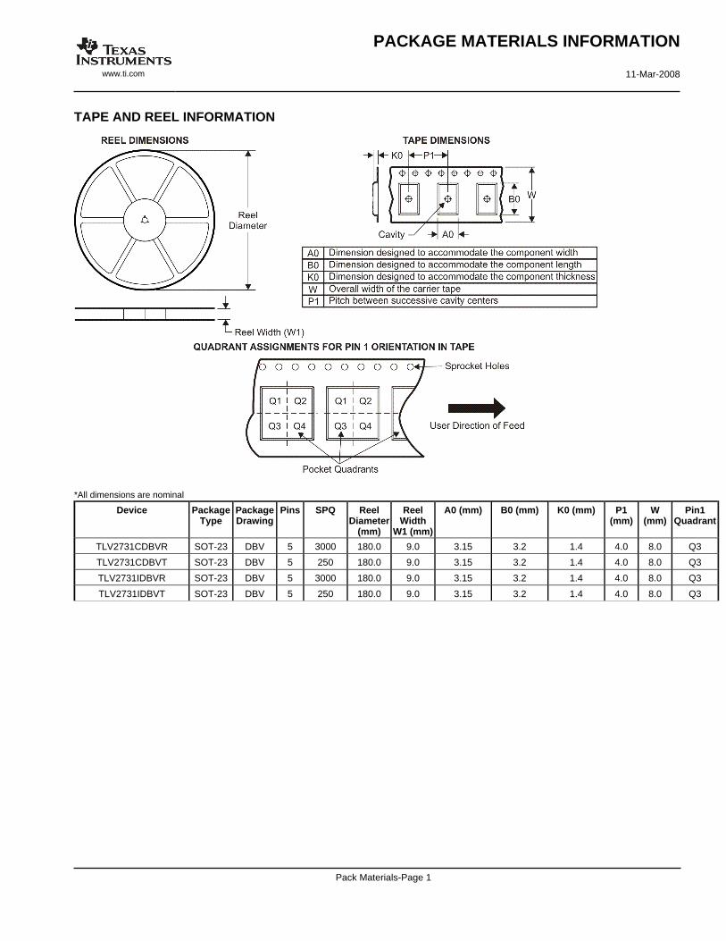
TAPE AND REEL INFORMATION
*All dimensions are nominal
Device PackageType
PackageDrawing
Pins SPQ ReelDiameter
(mm)
ReelWidth
W1 (mm)
A0 (mm) B0 (mm) K0 (mm) P1(mm)
W(mm)
Pin1Quadrant
TLV2731CDBVR SOT-23 DBV 5 3000 180.0 9.0 3.15 3.2 1.4 4.0 8.0 Q3
TLV2731CDBVT SOT-23 DBV 5 250 180.0 9.0 3.15 3.2 1.4 4.0 8.0 Q3
TLV2731IDBVR SOT-23 DBV 5 3000 180.0 9.0 3.15 3.2 1.4 4.0 8.0 Q3
TLV2731IDBVT SOT-23 DBV 5 250 180.0 9.0 3.15 3.2 1.4 4.0 8.0 Q3
PACKAGE MATERIALS INFORMATION
www.ti.com 11-Mar-2008
Pack Materials-Page 1
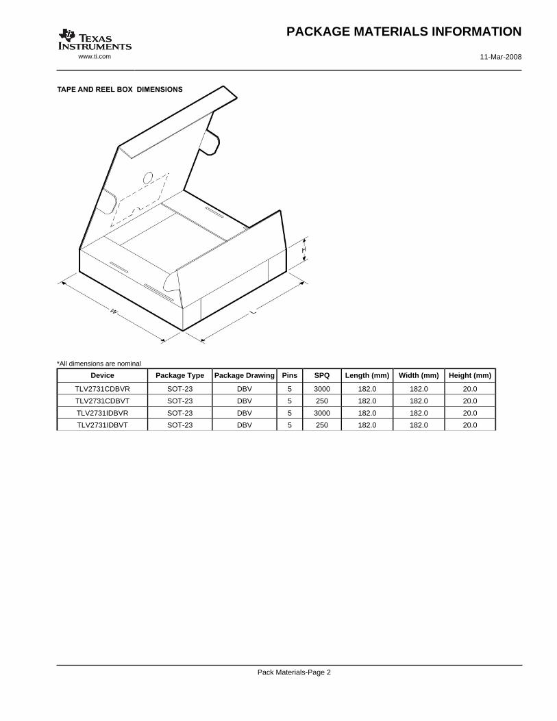
*All dimensions are nominal
Device Package Type Package Drawing Pins SPQ Length (mm) Width (mm) Height (mm)
TLV2731CDBVR SOT-23 DBV 5 3000 182.0 182.0 20.0
TLV2731CDBVT SOT-23 DBV 5 250 182.0 182.0 20.0
TLV2731IDBVR SOT-23 DBV 5 3000 182.0 182.0 20.0
TLV2731IDBVT SOT-23 DBV 5 250 182.0 182.0 20.0
PACKAGE MATERIALS INFORMATION
www.ti.com 11-Mar-2008
Pack Materials-Page 2
IMPORTANT NOTICETexas Instruments Incorporated and its subsidiaries (TI) reserve the right to make corrections, modifications, enhancements, improvements,and other changes to its products and services at any time and to discontinue any product or service without notice. Customers shouldobtain the latest relevant information before placing orders and should verify that such information is current and complete. All products aresold subject to TI’s terms and conditions of sale supplied at the time of order acknowledgment.TI warrants performance of its hardware products to the specifications applicable at the time of sale in accordance with TI’s standardwarranty. Testing and other quality control techniques are used to the extent TI deems necessary to support this warranty. Except wheremandated by government requirements, testing of all parameters of each product is not necessarily performed.TI assumes no liability for applications assistance or customer product design. Customers are responsible for their products andapplications using TI components. To minimize the risks associated with customer products and applications, customers should provideadequate design and operating safeguards.TI does not warrant or represent that any license, either express or implied, is granted under any TI patent right, copyright, mask work right,or other TI intellectual property right relating to any combination, machine, or process in which TI products or services are used. Informationpublished by TI regarding third-party products or services does not constitute a license from TI to use such products or services or awarranty or endorsement thereof. Use of such information may require a license from a third party under the patents or other intellectualproperty of the third party, or a license from TI under the patents or other intellectual property of TI.Reproduction of TI information in TI data books or data sheets is permissible only if reproduction is without alteration and is accompaniedby all associated warranties, conditions, limitations, and notices. Reproduction of this information with alteration is an unfair and deceptivebusiness practice. TI is not responsible or liable for such altered documentation. Information of third parties may be subject to additionalrestrictions.Resale of TI products or services with statements different from or beyond the parameters stated by TI for that product or service voids allexpress and any implied warranties for the associated TI product or service and is an unfair and deceptive business practice. TI is notresponsible or liable for any such statements.TI products are not authorized for use in safety-critical applications (such as life support) where a failure of the TI product would reasonablybe expected to cause severe personal injury or death, unless officers of the parties have executed an agreement specifically governingsuch use. Buyers represent that they have all necessary expertise in the safety and regulatory ramifications of their applications, andacknowledge and agree that they are solely responsible for all legal, regulatory and safety-related requirements concerning their productsand any use of TI products in such safety-critical applications, notwithstanding any applications-related information or support that may beprovided by TI. Further, Buyers must fully indemnify TI and its representatives against any damages arising out of the use of TI products insuch safety-critical applications.TI products are neither designed nor intended for use in military/aerospace applications or environments unless the TI products arespecifically designated by TI as military-grade or "enhanced plastic." Only products designated by TI as military-grade meet militaryspecifications. Buyers acknowledge and agree that any such use of TI products which TI has not designated as military-grade is solely atthe Buyer's risk, and that they are solely responsible for compliance with all legal and regulatory requirements in connection with such use.TI products are neither designed nor intended for use in automotive applications or environments unless the specific TI products aredesignated by TI as compliant with ISO/TS 16949 requirements. Buyers acknowledge and agree that, if they use any non-designatedproducts in automotive applications, TI will not be responsible for any failure to meet such requirements.Following are URLs where you can obtain information on other Texas Instruments products and application solutions:Products ApplicationsAmplifiers amplifier.ti.com Audio www.ti.com/audioData Converters dataconverter.ti.com Automotive www.ti.com/automotiveDSP dsp.ti.com Broadband www.ti.com/broadbandClocks and Timers www.ti.com/clocks Digital Control www.ti.com/digitalcontrolInterface interface.ti.com Medical www.ti.com/medicalLogic logic.ti.com Military www.ti.com/militaryPower Mgmt power.ti.com Optical Networking www.ti.com/opticalnetworkMicrocontrollers microcontroller.ti.com Security www.ti.com/securityRFID www.ti-rfid.com Telephony www.ti.com/telephonyRF/IF and ZigBee® Solutions www.ti.com/lprf Video & Imaging www.ti.com/video
Wireless www.ti.com/wireless
Mailing Address: Texas Instruments, Post Office Box 655303, Dallas, Texas 75265Copyright © 2008, Texas Instruments Incorporated


![LinCMOS Programmable Low-Power Operational ......Title LinCMOS Programmable Low-Power Operational Amplifiers (Rev. D) Author Texas Instruments, Incorporated [SLOS090,D ]](https://img.dokumen.tips/doc/110x75/60c520663ed5937ead0851c0/lincmos-programmable-low-power-operational-title-lincmos-programmable-low-power.jpg)