Embed Size (px)
Citation preview
|VDD ±| − Supply Voltage (V)
10
8
6
4
12
14
16
TA = 25°C
IO = ±50 µA
IO = ±500 µA
V(O
PP
)−
Ma
xim
um
Pe
ak-t
o-P
ea
k O
utp
ut
Vo
lta
ge
(V
)V
O(P
P)
4 6 8 10 12 14 16
Product
Folder
Sample &Buy
Technical
Documents
Tools &
Software
Support &Community
TLC2274-HTSGLS416 –JANUARY 2015
TLC2274-HT Advanced LinCMOS™ Rail-to-Rail Operational Amplifier1 Features 3 Description
The TLC2274 is a quadruple operational amplifier1• Qualified for Automotive Applications
from Texas Instruments. The device exhibits rail-to-• Qualified in Accordance With AEC-Q100 rail output performance for increased dynamic range• Output Swing Includes Both Supply Rails in single- or split-supply applications. The TLC2274
offers 2 MHz of bandwidth and 3 V/μs of slew rate for• Low Noise: 9 nV/√Hz Typ at ƒ = 1 kHzhigher speed applications. These device offers• Low Input Bias Current: 1 pA Typical comparable ac performance while having better
• Fully Specified for Both Single-Supply and Split- noise, input offset voltage, and power dissipation thanSupply Operation existing CMOS operational amplifiers. The TLC2274
has a noise voltage of 9nV/√Hz, two times lower than• Common-Mode Input Voltage Range Includescompetitive solutions.Negative Rail
• High-Gain Bandwidth: 2.2 MHz Typical The TLC2274, exhibiting high input impedance andlow noise, is excellent for small-signal conditioning for• High Slew Rate: 3.6 V/μs Typicalhigh-impedance sources, such as piezoelectric• Low Input Offset Voltage 2500-μV Max at TA = transducers. Because of the micropower dissipation
25°C levels, this device works well in hand-held monitoring• Macromodel Included and remote-sensing applications. In addition, the rail-
to-rail output feature, with single- or split-supplies,makes this device a great choice when interfacing2 Applicationswith analog-to-digital converters (ADCs). This family• Supports Extreme Temperature Applications: is fully characterized at 5 V and ±5 V.
– Controlled BaselineIt offers increased output dynamic range, lower noise
– One Assembly and Test Site voltage, and lower input offset voltage. This– One Fabrication Site enhanced feature set allows the device to be used in
a wider range of applications.– Available in Extreme (–40°C to 150°C)Temperature Range (1)
Device Information(1)– Extended Product Life Cycle
PART NUMBER PACKAGE BODY SIZE (NOM)– Extended Product-Change Notification TLC2274-HT TSSOP (14) 6.60 mm × 5.10 mm– Product Traceability
(1) For all available packages, see the orderable addendum at– Texas Instruments' high temperature products the end of the data sheet.
use highly-optimized silicon (die) solutions withMaximum Peak-to-Peak Output Voltagedesign and process enhancements to
vs Supply Voltagemaximize performance over extendedtemperatures. All devices are characterizedand qualified for 1000 hours continuousoperating life at maximum rated temperature.
(1) Custom temperature ranges available
1
An IMPORTANT NOTICE at the end of this data sheet addresses availability, warranty, changes, use in safety-critical applications,intellectual property matters and other important disclaimers. PRODUCTION DATA.
TLC2274-HTSGLS416 –JANUARY 2015 www.ti.com
Table of Contents7.1 Overview ................................................................. 171 Features .................................................................. 17.2 Functional Block Diagram ....................................... 172 Applications ........................................................... 17.3 Feature Description................................................. 173 Description ............................................................. 1
8 Application and Implementation ........................ 184 Revision History..................................................... 28.1 Application Information............................................ 185 Pin Configuration and Functions ......................... 38.2 Typical Application ................................................. 196 Specifications......................................................... 4
9 Power Supply Recommendations ...................... 226.1 Absolute Maximum Ratings ...................................... 410 Layout................................................................... 226.2 ESD Ratings.............................................................. 4
10.1 Layout Guidelines ................................................. 226.3 Recommended Operating Conditions....................... 410.2 Layout Example .................................................... 226.4 Thermal Information .................................................. 4
11 Device and Documentation Support ................. 236.5 Electrical Characteristics, VDD = 5 V......................... 511.1 Trademarks ........................................................... 236.6 Operating Characteristics, VDD = 5 V ....................... 611.2 Electrostatic Discharge Caution............................ 236.7 Electrical Characteristics, VDD± = ±5 V ..................... 711.3 Glossary ................................................................ 236.8 Operating Characteristics, VDD± = ±5 V .................... 8
12 Mechanical, Packaging, and Orderable6.9 Typical Characteristics ............................................ 10Information ........................................................... 237 Detailed Description ............................................ 17
4 Revision History
DATE REVISION NOTESJanuary 2015 * Initial release.
2 Submit Documentation Feedback Copyright © 2015, Texas Instruments Incorporated
Product Folder Links: TLC2274-HT
Q3 Q6 Q9 Q12 Q14 Q16
Q2 Q5 Q7 Q8 Q10 Q11
D1
Q17Q15Q13
Q4Q1
R5
C1
VDD+
IN+
IN−
R3 R4 R1 R2
OUT
VDD−
TLC2274-HTwww.ti.com SGLS416 –JANUARY 2015
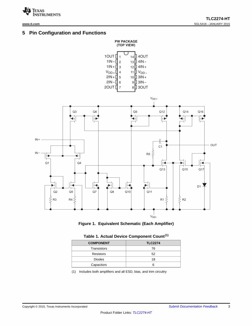
5 Pin Configuration and Functions
Figure 1. Equivalent Schematic (Each Amplifier)
Table 1. Actual Device Component Count (1)
COMPONENT TLC2274Transistors 76Resistors 52Diodes 18
Capacitors 6
(1) Includes both amplifiers and all ESD, bias, and trim circuitry
Copyright © 2015, Texas Instruments Incorporated Submit Documentation Feedback 3
Product Folder Links: TLC2274-HT
TLC2274-HTSGLS416 –JANUARY 2015 www.ti.com
6 Specifications
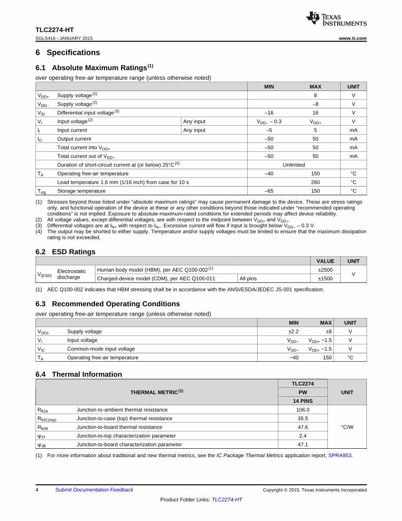
6.1 Absolute Maximum Ratings (1)
over operating free-air temperature range (unless otherwise noted)MIN MAX UNIT
VDD+ Supply voltage (2) 8 VVDD– Supply voltage (2) –8 VVID Differential input voltage (3) –16 16 VVI Input voltage (2) Any input VDD– – 0.3 VDD+ VII Input current Any input –5 5 mAIO Output current –50 50 mA
Total current into VDD+ –50 50 mATotal current out of VDD− –50 50 mADuration of short-circuit current at (or below) 25°C (4) Unlimited
TA Operating free-air temperature –40 150 °CLead temperature 1.6 mm (1/16 inch) from case for 10 s 260 °C
Tstg Storage temperature –65 150 °C
(1) Stresses beyond those listed under “absolute maximum ratings” may cause permanent damage to the device. These are stress ratingsonly, and functional operation of the device at these or any other conditions beyond those indicated under “recommended operatingconditions” is not implied. Exposure to absolute-maximum-rated conditions for extended periods may affect device reliability.
(2) All voltage values, except differential voltages, are with respect to the midpoint between VDD+ and VDD–.(3) Differential voltages are at IN+ with respect to IN–. Excessive current will flow if input is brought below VDD– – 0.3 V.(4) The output may be shorted to either supply. Temperature and/or supply voltages must be limited to ensure that the maximum dissipation
rating is not exceeded.
6.2 ESD RatingsVALUE UNIT
Human-body model (HBM), per AEC Q100-002 (1) ±2500ElectrostaticV(ESD) Vdischarge Charged-device model (CDM), per AEC Q100-011 All pins ±1500
(1) AEC Q100-002 indicates that HBM stressing shall be in accordance with the ANSI/ESDA/JEDEC JS-001 specification.
6.3 Recommended Operating Conditionsover operating free-air temperature range (unless otherwise noted)
MIN MAX UNITVDD± Supply voltage ±2.2 ±8 VVI Input voltage VDD− VDD+ −1.5 VVIC Common-mode input voltage VDD− VDD+ −1.5 VTA Operating free-air temperature −40 150 °C
6.4 Thermal InformationTLC2274
THERMAL METRIC (1) PW UNIT14 PINS
RθJA Junction-to-ambient thermal resistance 106.0RθJC(top) Junction-to-case (top) thermal resistance 35.5RθJB Junction-to-board thermal resistance 47.6 °C/WψJT Junction-to-top characterization parameter 2.4ψJB Junction-to-board characterization parameter 47.1
(1) For more information about traditional and new thermal metrics, see the IC Package Thermal Metrics application report, SPRA953.
4 Submit Documentation Feedback Copyright © 2015, Texas Instruments Incorporated
Product Folder Links: TLC2274-HT
TLC2274-HTwww.ti.com SGLS416 –JANUARY 2015
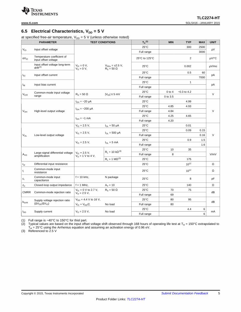
6.5 Electrical Characteristics, VDD = 5 Vat specified free-air temperature, VDD = 5 V (unless otherwise noted)
PARAMETER TEST CONDITIONS TA(1) MIN TYP MAX UNIT
25°C 300 2500VIO Input offset voltage μV
Full range 3000
Temperature coefficient ofαVIO 25°C to 125°C 2 μV/°Cinput offset voltage
Input offset voltage long-term VIC = 0 V, VDD± = ±2.5 V, 25°C 0.002 μV/modrift (2)VO = 0 V, RS = 50 Ω
25°C 0.5 60IIO Input offset current pA
Full range 7000
25°C 1IIB Input bias current pA
Full range
25°C 0 to 4 −0.3 to 4.2Common-mode input voltageVICR RS = 50 Ω |VIO| ≤ 5 mV Vrange Full range 0 to 3.5
IOH = −20 μA 25°C 4.99
25°C 4.85 4.93IOH = −200 μA
VOH High-level output voltage Full range 4.84 V
25°C 4.25 4.65IOH = −1 mA
Full range 4.20
VIC = 2.5 V, IOL = 50 μA 25°C 0.01
25°C 0.09 0.15VIC = 2.5 V, IOL = 500 μA
VOL Low-level output voltage Full range 0.16 V
25°C 0.9 1.5VIC = 2.5 V, IOL = 5 mA
Full range 1.6
25°C 10 35RL = 10 kΩ (3)
Large-signal differential voltage VIC = 2.5 V,AVD Full range 8 V/mVamplification VO = 1 V to 4 V,RL = 1 MΩ (3) 25°C 175
Differential input resistancerid 25°C Ω1012
Common-mode inputri 25°C Ω1012resistance
Common-mode input f = 10 kHz, N packageci 25°C 8 pFcapacitance
zo Closed-loop output impedance f = 1 MHz, AV = 10 25°C 140 Ω
VIC = 0 V to 2.7 V, RS = 50 Ω 25°C 70 75CMRR Common-mode rejection ratio dBVO = 2.5 V, Full range 69
VDD = 4.4 V to 16 V, 25°C 80 95Supply voltage rejection ratiokSVR dB(ΔVDD/ΔVIO) VIC = VDD/2, No load Full range 80
25°C 4.4 6IDD Supply current VO = 2.5 V, No load mA
Full range 6
(1) Full range is −40°C to 150°C for thisl part.(2) Typical values are based on the input offset voltage shift observed through 168 hours of operating life test at TA = 150°C extrapolated to
TA = 25°C using the Arrhenius equation and assuming an activation energy of 0.96 eV.(3) Referenced to 2.5 V
Copyright © 2015, Texas Instruments Incorporated Submit Documentation Feedback 5
Product Folder Links: TLC2274-HT
TLC2274-HTSGLS416 –JANUARY 2015 www.ti.com
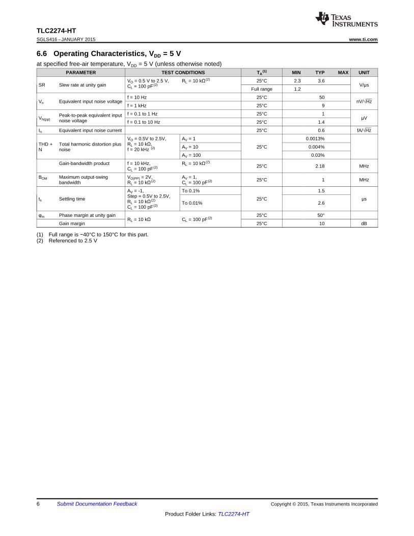
6.6 Operating Characteristics, VDD = 5 Vat specified free-air temperature, VDD = 5 V (unless otherwise noted)
PARAMETER TEST CONDITIONS TA(1) MIN TYP MAX UNIT
VO = 0.5 V to 2.5 V, RL = 10 kΩ (2) 25°C 2.3 3.6SR Slew rate at unity gain V/μsCL = 100 pF (2)
Full range 1.2
f = 10 Hz 25°C 50Vn Equivalent input noise voltage nV/√Hz
f = 1 kHz 25°C 9
f = 0.1 to 1 Hz 25°C 1Peak-to-peak equivalent inputVN(pp) μVnoise voltage f = 0.1 to 10 Hz 25°C 1.4
In Equivalent input noise current 25°C 0.6 fA/√Hz
VO = 0.5V to 2.5V, AV = 1 0.0013%RL = 10 kΩ,THD + Total harmonic distortion plus AV = 10 25°C 0.004%f = 20 kHz (2)N noise
AV = 100 0.03%
Gain-bandwidth product f = 10 kHz, RL = 10 kΩ (2)25°C 2.18 MHzCL = 100 pF(2)
BOM Maximum output-swing VO(PP) = 2V, AV = 1, 25°C 1 MHzbandwidth RL = 10 kΩ (2) CL = 100 pF(2)
AV = -1, To 0.1% 1.5Step = 0.5V to 2.5V,ts Settling time 25°C μsRL = 10 kΩ (2)
To 0.01% 2.6CL = 100 pF(2)
φm Phase margin at unity gain 25°C 50°RL = 10 kΩ CL = 100 pF(2)
Gain margin 25°C 10 dB
(1) Full range is −40°C to 150°C for this part.(2) Referenced to 2.5 V
6 Submit Documentation Feedback Copyright © 2015, Texas Instruments Incorporated
Product Folder Links: TLC2274-HT
TLC2274-HTwww.ti.com SGLS416 –JANUARY 2015
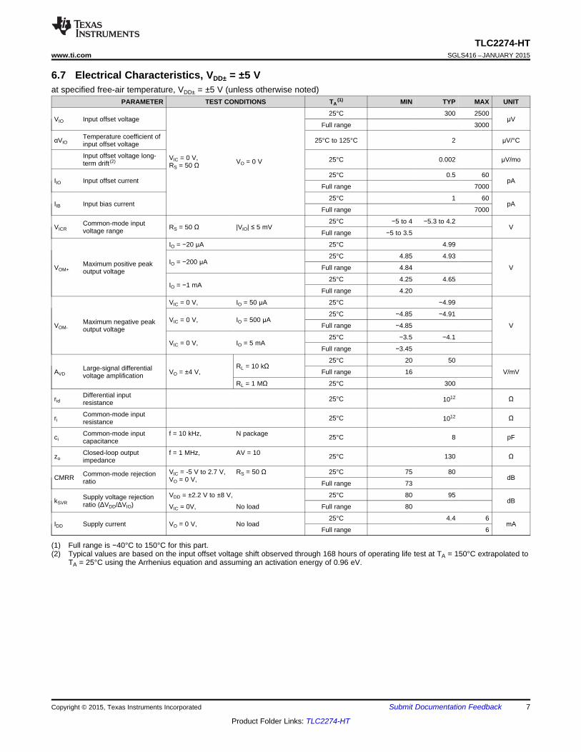
6.7 Electrical Characteristics, VDD± = ±5 Vat specified free-air temperature, VDD± = ±5 V (unless otherwise noted)
PARAMETER TEST CONDITIONS TA(1) MIN TYP MAX UNIT
25°C 300 2500VIO Input offset voltage μV
Full range 3000
Temperature coefficient ofαVIO 25°C to 125°C 2 μV/°Cinput offset voltage
Input offset voltage long- VIC = 0 V, 25°C 0.002 μV/moVO = 0 Vterm drift (2)RS = 50 Ω
25°C 0.5 60IIO Input offset current pA
Full range 7000
25°C 1 60IIB Input bias current pA
Full range 7000
25°C −5 to 4 −5.3 to 4.2Common-mode inputVICR RS = 50 Ω |VIO| ≤ 5 mV Vvoltage range Full range −5 to 3.5
IO = −20 μA 25°C 4.99
25°C 4.85 4.93IO = −200 μAMaximum positive peakVOM+ Full range 4.84 Voutput voltage
25°C 4.25 4.65IO = −1 mA
Full range 4.20
VIC = 0 V, IO = 50 μA 25°C −4.99
25°C −4.85 −4.91VIC = 0 V, IO = 500 μAMaximum negative peakVOM- Full range −4.85 Voutput voltage
25°C −3.5 −4.1VIC = 0 V, IO = 5 mA
Full range −3.45
25°C 20 50RL = 10 kΩLarge-signal differentialAVD VO = ±4 V, Full range 16 V/mVvoltage amplificationRL = 1 MΩ 25°C 300
Differential inputrid 25°C Ω1012resistance
Common-mode inputri 25°C Ω1012resistance
Common-mode input f = 10 kHz, N packageci 25°C 8 pFcapacitance
Closed-loop output f = 1 MHz, AV = 10zo 25°C 130 Ωimpedance
VIC = -5 V to 2.7 V, RS = 50 Ω 25°C 75 80Common-mode rejectionCMRR dBVO = 0 V,ratio Full range 73
VDD = ±2.2 V to ±8 V, 25°C 80 95Supply voltage rejectionkSVR dBratio (ΔVDD/ΔVIO) VIC = 0V, No load Full range 80
25°C 4.4 6IDD Supply current VO = 0 V, No load mA
Full range 6
(1) Full range is −40°C to 150°C for this part.(2) Typical values are based on the input offset voltage shift observed through 168 hours of operating life test at TA = 150°C extrapolated to
TA = 25°C using the Arrhenius equation and assuming an activation energy of 0.96 eV.
Copyright © 2015, Texas Instruments Incorporated Submit Documentation Feedback 7
Product Folder Links: TLC2274-HT
Continuous TJ (°C)
Es
tim
ate
dL
ife
(ye
ars
)
110 120 130 140 150 160 170 180
1
2
3
5
10
20
30
50
100
200
300
500
1000
D006
Electromigration Fail Mode
TLC2274-HTSGLS416 –JANUARY 2015 www.ti.com
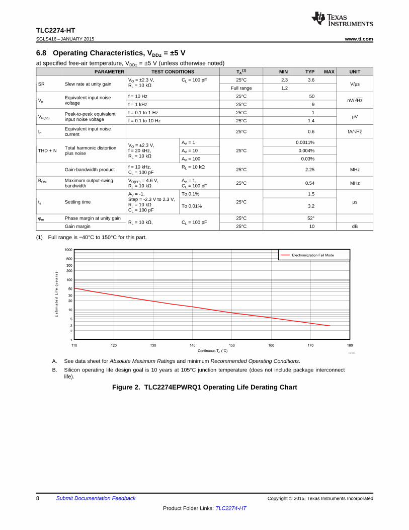
6.8 Operating Characteristics, VDD± = ±5 Vat specified free-air temperature, VDD± = ±5 V (unless otherwise noted)
PARAMETER TEST CONDITIONS TA(1) MIN TYP MAX UNIT
VO = ±2.3 V, CL = 100 pF 25°C 2.3 3.6SR Slew rate at unity gain V/μsRL = 10 kΩ Full range 1.2
f = 10 Hz 25°C 50Equivalent input noiseVn nV/√Hzvoltage f = 1 kHz 25°C 9
f = 0.1 to 1 Hz 25°C 1Peak-to-peak equivalentVN(pp) μVinput noise voltage f = 0.1 to 10 Hz 25°C 1.4
Equivalent input noiseIn 25°C 0.6 fA/√Hzcurrent
AV = 1 0.0011%VO = ±2.3 V,Total harmonic distortionTHD + N f = 20 kHz, AV = 10 25°C 0.004%plus noise RL = 10 kΩ AV = 100 0.03%
f = 10 kHz, RL = 10 kΩGain-bandwidth product 25°C 2.25 MHzCL = 100 pF
BOM Maximum output-swing VO(PP) = 4.6 V, AV = 1, 25°C 0.54 MHzbandwidth RL = 10 kΩ CL = 100 pF
AV = -1, To 0.1% 1.5Step = -2.3 V to 2.3 V,ts Settling time 25°C μsRL = 10 kΩ To 0.01% 3.2CL = 100 pF
φm Phase margin at unity gain 25°C 52°RL = 10 kΩ, CL = 100 pF
Gain margin 25°C 10 dB
(1) Full range is −40°C to 150°C for this part.
A. See data sheet for Absolute Maximum Ratings and minimum Recommended Operating Conditions.B. Silicon operating life design goal is 10 years at 105°C junction temperature (does not include package interconnect
life).
Figure 2. TLC2274EPWRQ1 Operating Life Derating Chart
8 Submit Documentation Feedback Copyright © 2015, Texas Instruments Incorporated
Product Folder Links: TLC2274-HT
Tim
e to
Fai
l (ho
urs)
Continuous TJ (°C)
R2 = 0.831049146721252
TLC2274-HTwww.ti.com SGLS416 –JANUARY 2015
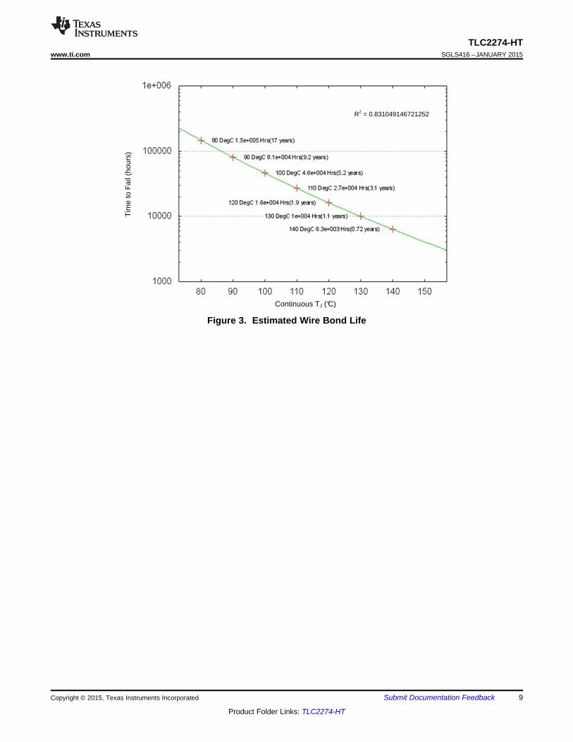
Figure 3. Estimated Wire Bond Life
Copyright © 2015, Texas Instruments Incorporated Submit Documentation Feedback 9
Product Folder Links: TLC2274-HT
−75 − 25 0 25 50 75 100 125
2
1
0
−1
3
4
5
−In
pu
t V
olta
ge
−V
VI
TA − Free-Air Temperature − °C
|VIO| ≤ 5mV
VDD = 5 V
− 50
V0H
−H
igh-L
evel O
utp
ut V
oltage
−V
VO
H
IOH − High-Level Output Current − mA
4
2
1
0
6
3
0 1 2 3 4
5
VDD = 5 V
0
− 2
− 6
− 8
− 10
8
− 4
2 3 4 5 6 7 8
−In
put V
oltage
−V 4
2
6
10
|VDD±| − Supply Voltage − V
VI
TA = 25°C
RS = 50 Ω
|VIO| ≤ 5mV
12
0.5
0
−1−1 0 1
VIO
−In
pu
t O
ffse
t V
olta
ge
−m
V
1
2 3 4 5
VIC − Common-Mode Voltage − V
VIO
−0.5
VDD = ±5 V
TA = 25°C
RS = 50 Ω
−6 −5 −4 −3 −2
VIO − Input Offset V oltage − mV
Perc
enta
ge o
fA
mplif
iers
−%
10
5
0
20
15
0 0.4 0.8 1.2 1.6
992 Amplifiers From
−1.6 −1.2 −0.8 −0.4
2 Wafer Lots
VDD = ±2.5 V
0.5
0
−1−1 0 1
VIO
−In
pu
t O
ffse
t V
olta
ge
−m
V
1
2 3 4 5
VIO
VIC − Common-Mode Voltage − V
VDD = 5 V
TA = 25°C
RS = 50 Ω
−0.5
TLC2274-HTSGLS416 –JANUARY 2015 www.ti.com
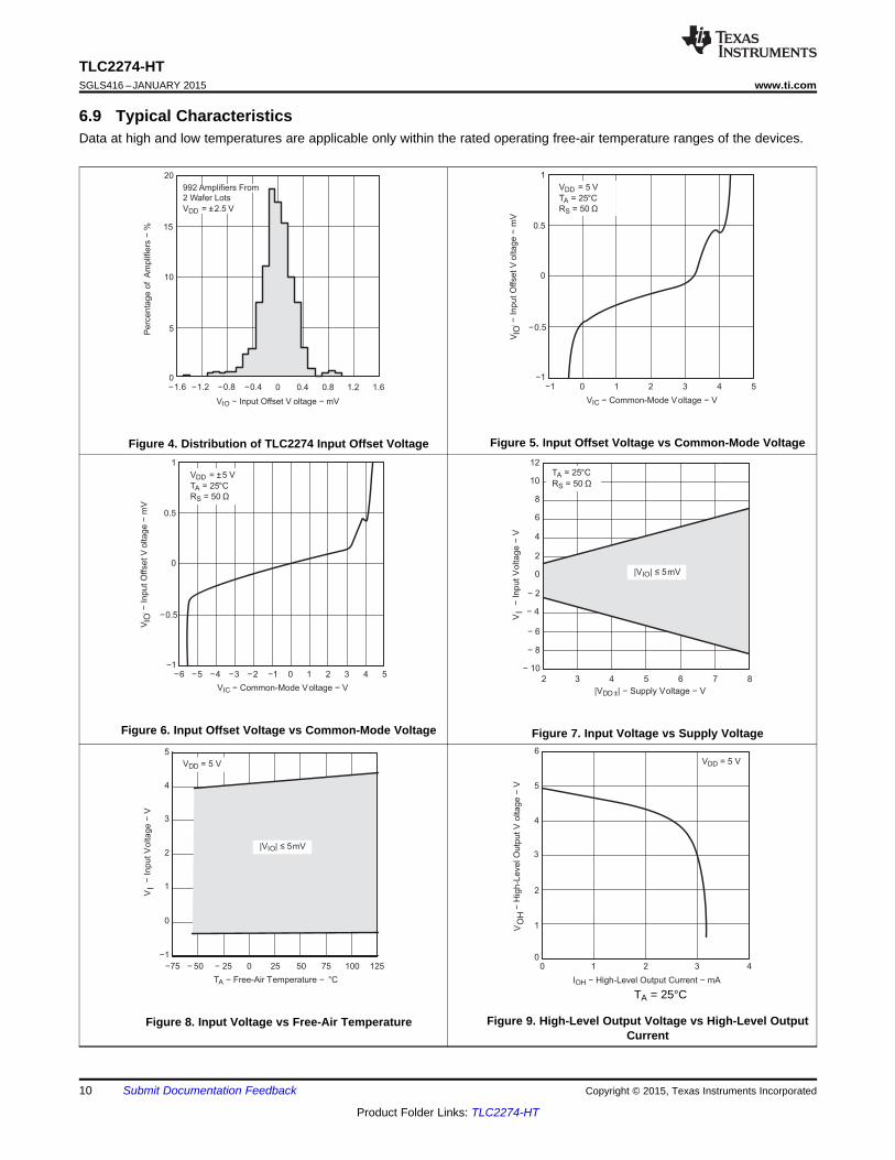
6.9 Typical CharacteristicsData at high and low temperatures are applicable only within the rated operating free-air temperature ranges of the devices.
Figure 5. Input Offset Voltage vs Common-Mode VoltageFigure 4. Distribution of TLC2274 Input Offset Voltage
Figure 6. Input Offset Voltage vs Common-Mode Voltage Figure 7. Input Voltage vs Supply Voltage
TA = 25°C
Figure 9. High-Level Output Voltage vs High-Level OutputFigure 8. Input Voltage vs Free-Air TemperatureCurrent
10 Submit Documentation Feedback Copyright © 2015, Texas Instruments Incorporated
Product Folder Links: TLC2274-HT
2
1
0
10 k 100 k 1 M
3
f − Frequency − Hz
4
10 M
6
5
7
8
9
10
V(O
PP
)−
Maxim
um
Peak-t
o-P
eak O
utp
ut V
oltage
−V
VO
(PP
)
VDD = 5 V
VDD = ±5 V
RL = 10 kΩ
TA = 25°C
4
0
2 3 4
8
12
16
5 6 7 8
IOS
−S
hort
-Circuit O
utp
ut C
urr
ent
−m
AO
SI
|VDD±| − Supply Voltage − V
VID = 100 mV
VO = 0 V
TA = 25°C
−8
VID = −100 mV
−4
3
2
10 1 2 3 4 5
−M
axim
um
Po
sitiv
e P
ea
k O
utp
ut
Vo
lta
ge
−V
4
5
|IO| − Output Current − mA
VDD± = ±5 V
VO
M +
0 1 2 3 4 5 6
IO − Output Current − mA
VDD = ±5 V
VIC = 0 V
−3.8
−4
−4.2
−4.4
−4.6
−4.8
−5
−M
axim
um
Ne
ga
tive
Pe
ak O
utp
ut
Vo
lta
ge
−V
VO
M−
VO
L−
Low
-Level O
utp
ut V
oltage
−V
0.6
0.4
0.2
00 1 2 3
0.8
4 5
VDD = 5 V
TA = 25°C
IOL − Low-Level Output Current − mA
VO
L
VIC = 1.25 V
1
1.2
VIC = 2.5 V
VIC = 0 V
VO
L−
Lo
w-L
eve
l O
utp
ut
Vo
lta
ge
−V
IOL − Low-Level Output Current − mA
VO
L
0.6
0.4
0.2
00 1 2 3
0.8
4
1
1.2
5 6
1.4VDD = 5 V
VIC = 2.5 V
TLC2274-HTwww.ti.com SGLS416 –JANUARY 2015
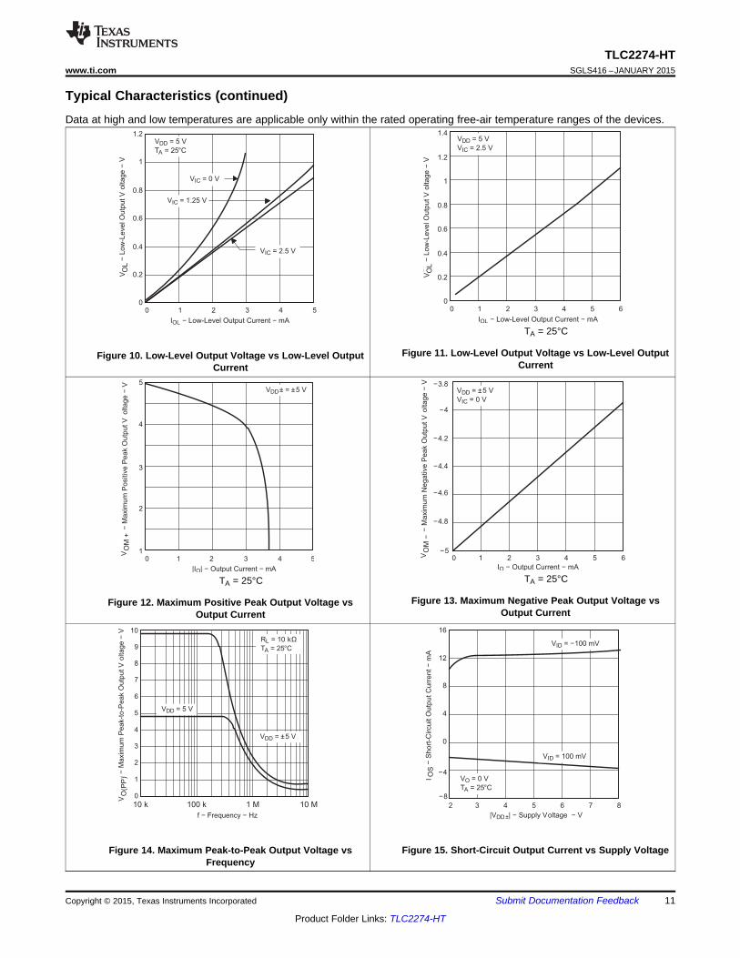
Typical Characteristics (continued)Data at high and low temperatures are applicable only within the rated operating free-air temperature ranges of the devices.
TA = 25°C
Figure 11. Low-Level Output Voltage vs Low-Level OutputFigure 10. Low-Level Output Voltage vs Low-Level OutputCurrentCurrent
TA = 25°CTA = 25°C
Figure 13. Maximum Negative Peak Output Voltage vsFigure 12. Maximum Positive Peak Output Voltage vsOutput CurrentOutput Current
Figure 15. Short-Circuit Output Current vs Supply VoltageFigure 14. Maximum Peak-to-Peak Output Voltage vsFrequency
Copyright © 2015, Texas Instruments Incorporated Submit Documentation Feedback 11
Product Folder Links: TLC2274-HT
0
20
1 k 10 k 100 k 1 M
40
60
80
f − Frequency − Hz
10 M
VDD = ±5 V
RL = 10 kΩ
CL = 100 pF
TA = 25°C
om
−P
ha
se
Ma
rgin
φm
−20
−40 −90°
−45°
0°
45°
90°
135°
180°
AV
D−
La
rge
-Sig
na
l D
iffe
ren
tia
lA
VD Vo
lta
ge
Am
plif
ica
tio
n−
dB
Free-Air Temperature, TA (°C)
AV
VD
D, L
arge
-Sig
nal D
iffer
entia
l V
olta
ge A
mpl
ifica
tion
(V/m
V)
-50 -25 0 25 50 75 100 125 150 175 2001
2
3
57
10
20
30
5070
100
D003
0
20
1 k 10 k 100 k 1 M
40
60
80
f − Frequency − Hz
10 M
om
−P
ha
se
Ma
rgin
φm
VDD = 5 V
RL = 10 kΩ
CL = 100 pF
TA = 25°C
−20
−40 −90°
−45°
0°
45°
90°
135°
180°
AV
D−
La
rge
-Sig
na
l D
iffe
ren
tia
lA
VD Vo
lta
ge
Am
plif
ica
tio
n−
dB
0.1
1
0.1 1 10 100
10
100
1000
RL − Load Resistance − k Ω
VO = ±1 V
TA = 25°C
VDD = ±5 V
VDD = 5 V
AV
D−
Larg
e-S
ignal D
iffe
rential
AV
D Voltage
Am
plif
ication
−dB
3
2
1
0800
4
5
1200
VID − Differential Input V oltage − µV
−O
utp
ut V
oltage
−V
VO
−800 −400 4000
VDD = 5 V
TA = 25°C
RL = 10 kΩ
VIC = 2.5 V
1
−1
−3
−50 250
3
5
500 750 1000
VID − Differential Input V oltage − µV
−O
utp
ut
Vo
lta
ge
−V
VO
−1000 −750 −250−500
VDD = ±5 V
TA = 25°C
RL = 10 kΩ
VIC = 0 V
TLC2274-HTSGLS416 –JANUARY 2015 www.ti.com
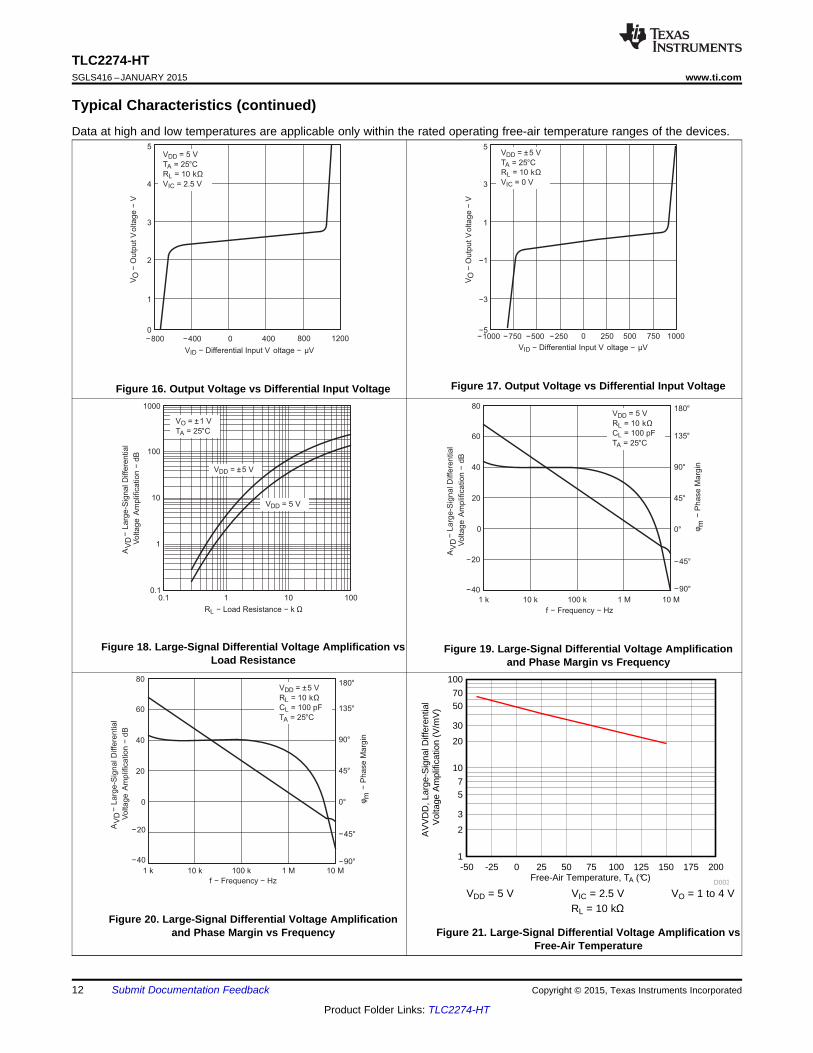
Typical Characteristics (continued)Data at high and low temperatures are applicable only within the rated operating free-air temperature ranges of the devices.
Figure 17. Output Voltage vs Differential Input VoltageFigure 16. Output Voltage vs Differential Input Voltage
Figure 18. Large-Signal Differential Voltage Amplification vs Figure 19. Large-Signal Differential Voltage AmplificationLoad Resistance and Phase Margin vs Frequency
VDD = 5 V VIC = 2.5 V VO = 1 to 4 VRL = 10 kΩ
Figure 20. Large-Signal Differential Voltage AmplificationFigure 21. Large-Signal Differential Voltage Amplification vsand Phase Margin vs Frequency
Free-Air Temperature
12 Submit Documentation Feedback Copyright © 2015, Texas Instruments Incorporated
Product Folder Links: TLC2274-HT

40
20
0
10 100 1 k
kS
VR
−S
up
ply
-Vo
lta
ge
Re
jectio
n R
atio
−d
B
60
80
f − Frequency − Hz
100
10 k 100 k 1 M 10 M
kS
VR
VDD = 5 V
TA = 25°C
kSVR+
kSVR−
−20
Free-Air Temperature, TA (°C)
Com
mon
-Mod
e R
ejec
tion
Rat
io, C
MR
R (
dB)
-50 0 50 100 150 20086
88
90
92
94
96
98
100
102
D005
VDD = 5 VVDD = ±5 V
10
1
0.1
1000
100
100 1 k 10 k 100 k 1 M
zo
−O
utp
ut Im
pedance
−W
f − Frequency − Hz
VDD = ±5 V
TA = 25°C
AV = 100
AV = 10
AV = 1
60
40
20
010 100 1 k 10 k
CM
RR
−C
om
mon-M
ode R
eje
ction R
atio
−dB
80
100
100 k 1 M
f − Frequency − Hz
VDD = ±5 V
VDD = 5 V
10 M
TA = 25°C
10
1
0.1
1000
100
100 1 k 10 k 100 k 1 M
zo
−O
utp
ut
Imp
ed
an
ce
−W
f − Frequency − Hz
VDD = 5 V
TA = 25°C
AV = 100
AV = 10
AV = 1
Free-Air Temperature, TA (°C)
AV
VD
D, L
arge
-Sig
nal D
iffer
entia
l V
olta
ge A
mpl
ifica
tion
(V/m
V)
-50 -25 0 25 50 75 100 125 150 175 2001
2
3
57
10
20
30
5070
100
D004
TLC2274-HTwww.ti.com SGLS416 –JANUARY 2015
Typical Characteristics (continued)Data at high and low temperatures are applicable only within the rated operating free-air temperature ranges of the devices.
VDD = ±5 V VIC = 2.5 V VO = ±4 VRL = 10 kΩ
Figure 23. Output Impedance vs FrequencyFigure 22. Large-Signal Differential Voltage Amplification vs
Free-Air Temperature
Figure 25. Common-Mode Rejection Ratio vs FrequencyFigure 24. Output Impedance vs Frequency
Figure 26. Common-Mode Rejection Ratio vs Free-Air Figure 27. Supply-Voltage Rejection Ratio vs FrequencyTemperature
Copyright © 2015, Texas Instruments Incorporated Submit Documentation Feedback 13
Product Folder Links: TLC2274-HT
0
− 1
− 3
− 4
− 5
4
− 2
1 2 3 4 5
2
1
3
5
6 7 8 9
VO
−O
utp
ut V
oltage
−V
VO
t − Time − µs
VDD = ±5 V
RL = 10 kΩ
CL = 100 pF
TA = 25°C
AV = −1
0
2
1
01 2 3 4 5
3
4
5
6 7 8 9
VO
−O
utp
ut
Vo
lta
ge
−m
VV
O
t − Time − µs
VDD = 5 V
RL = 10 kΩ
CL = 100 pF
TA = 25°C
AV = −1
0
Free-Air Temperature, TA (°C)
Sle
w R
ate,
SR
(V
/µs)
-50 0 50 100 150 2000
1
2
3
4
5
D001
65±
SR+
µs
SR
−S
lew
Ra
te−
V/
0
1
2
3
CL − Load Capacitance − pF
10 k1 k10010
SR +
SR −
4
5VDD = 5 V
AV = −1
TA = 25°C
40
20
0
10 100 1 k
kS
VR
−S
up
ply
-Vo
lta
ge
Re
jectio
n R
atio
−d
B
60
80
f − Frequency − Hz
100
10 k 100 k 1 M 10 M
kS
VR
VDD = ±5 V
TA = 25°C
kSVR+
kSVR−
−20
Free-Air Temperature, TA (°C)
kksS
SV
VR
R, S
uppl
y V
olta
ge
Rej
ectio
n R
atio
(dB
)
-50 0 50 100 150 20090
95
100
105
110
D002
TLC2274-HTSGLS416 –JANUARY 2015 www.ti.com
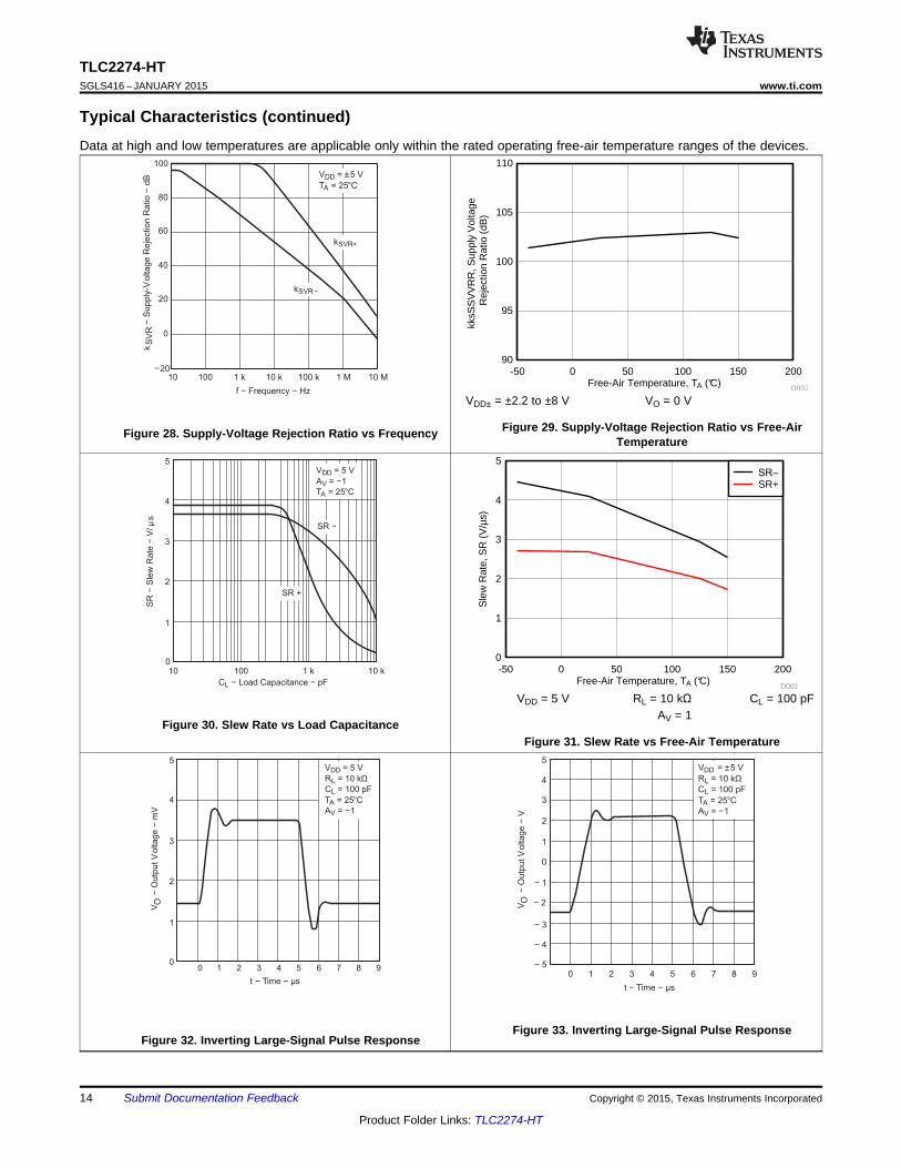
Typical Characteristics (continued)Data at high and low temperatures are applicable only within the rated operating free-air temperature ranges of the devices.
VDD± = ±2.2 to ±8 V VO = 0 V
Figure 29. Supply-Voltage Rejection Ratio vs Free-AirFigure 28. Supply-Voltage Rejection Ratio vs FrequencyTemperature
VDD = 5 V RL = 10 kΩ CL = 100 pFAV = 1
Figure 30. Slew Rate vs Load CapacitanceFigure 31. Slew Rate vs Free-Air Temperature
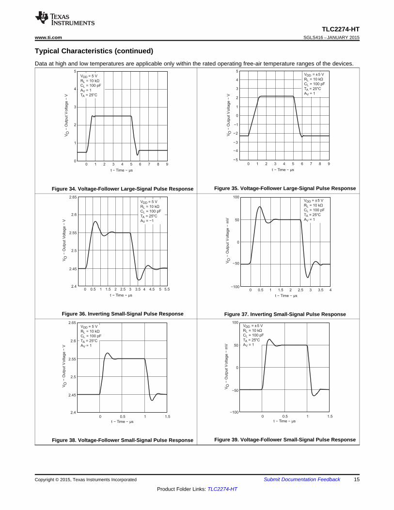
Figure 33. Inverting Large-Signal Pulse ResponseFigure 32. Inverting Large-Signal Pulse Response
14 Submit Documentation Feedback Copyright © 2015, Texas Instruments Incorporated
Product Folder Links: TLC2274-HT
2.5
2.45
2.4
2.55
2.6
0 0.5 1 1.5
VO
−O
utp
ut
Vo
lta
ge
−V
VO
t − Time − µs
2.65VDD = 5 V
RL = 10 kΩ
CL = 100 pF
TA = 25°C
AV = 1
0
−50
−100
50
100
0 0.5 1 1.5
VO
−O
utp
ut V
oltage
−m
VV
O
t − Time − µs
VDD = ±5 V
RL = 10 kΩ
CL = 100 pF
TA = 25°C
AV = 1
0
−1000 0.5 1 1.5 2
50
100
2.5 3 3.5 4
VO
−O
utp
ut V
oltage
−m
VV
O
t − Time − µs
VDD = ±5 V
RL = 10 kΩ
CL = 100 pF
TA = 25°C
AV = 1
−50
2.5
2.45
2.40.5 1 1.5 2 2.5
2.55
2.6
2.65
3.5 4.5 5 5.5
−O
utp
ut V
oltage
−V
VO
t − Time − µs
VDD = 5 V
RL = 10 kΩ
CL = 100 pF
TA = 25°C
AV = −1
0 3 4
3
2
1
01 2 3 4 5
4
5
6 7 8 9
VO
−O
utp
ut
Vo
lta
ge
−V
VO
t − Time − µs
VDD = 5 V
RL = 10 kΩ
CL = 100 pF
AV = 1
TA = 25°C
0
0
−1
4
1 2 3 4 5
2
1
3
5
6 7 8 9
VO
−O
utp
ut V
oltage
−V
VO
t − Time − µs
VDD = ±5 V
RL = 10 kΩ
CL = 100 pF
TA = 25°C
AV = 1
0
−2
−3
−5
−4
TLC2274-HTwww.ti.com SGLS416 –JANUARY 2015
Typical Characteristics (continued)Data at high and low temperatures are applicable only within the rated operating free-air temperature ranges of the devices.
Figure 35. Voltage-Follower Large-Signal Pulse ResponseFigure 34. Voltage-Follower Large-Signal Pulse Response
Figure 36. Inverting Small-Signal Pulse Response Figure 37. Inverting Small-Signal Pulse Response
Figure 39. Voltage-Follower Small-Signal Pulse ResponseFigure 38. Voltage-Follower Small-Signal Pulse Response
Copyright © 2015, Texas Instruments Incorporated Submit Documentation Feedback 15
Product Folder Links: TLC2274-HT
0.0001
0.001
100 1 k 10 k 100 k
TH
D +
N−
Tota
l H
arm
onic
Dis
tort
ion P
lus N
ois
e−
%
f − Frequency − Hz
0.01
0.1
1
VDD = 5 V
TA = 25°C
RL = 10 kΩ
AV = 100
AV = 10
AV = 1
Gain
-Bandw
idth
Pro
duct
−M
Hz
2.1
20 1 2 3 4 5
2.2
2.3
6 7 8
|VDD±| − Supply Voltage − V
2.4
2.5
f = 10 kHz
RL = 10 kΩ
CL = 100 pF
TA = 25°C
Inte
gra
ted N
ois
e V
oltage
−uV
RM
S
1
0.1
100
1 10 100 1 k
f − Frequency − Hz
10 k 100 k
VR
MS
µ
Calculated UsingIdeal Pass-Band FilterLower Frequency = 1 HzTA= 25°C
10
−750
−10002 4 6
0
250
8 10
Nois
e V
oltage
−nV
t − Time − s
0
VDD = 5 V
f = 0.1 Hz to 10 Hz
TA = 25°C
500
750
1000
−250
−500
20
10
010 100 1 k
Vn
−E
qu
iva
len
t In
pu
t N
ois
e V
olta
ge
−n
V H
z
30
f − Frequency − Hz
40
10 k
50
60
Vn
nV
/H
z VDD = 5 V
TA = 25°C
RS = 20 Ω
20
10
010 100 1 k
Vn
−E
quiv
ale
nt In
put N
ois
e V
oltage
−nV
Hz
30
f − Frequency − Hz
40
10 k
50
60
Vn
nV
/H
z
VDD = ±5 V
TA = 25°C
RS = 20 Ω
TLC2274-HTSGLS416 –JANUARY 2015 www.ti.com
Typical Characteristics (continued)Data at high and low temperatures are applicable only within the rated operating free-air temperature ranges of the devices.
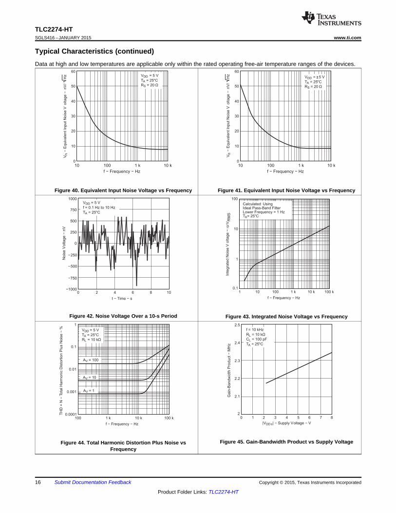
Figure 40. Equivalent Input Noise Voltage vs Frequency Figure 41. Equivalent Input Noise Voltage vs Frequency
Figure 42. Noise Voltage Over a 10-s Period Figure 43. Integrated Noise Voltage vs Frequency
Figure 45. Gain-Bandwidth Product vs Supply VoltageFigure 44. Total Harmonic Distortion Plus Noise vsFrequency
16 Submit Documentation Feedback Copyright © 2015, Texas Instruments Incorporated
Product Folder Links: TLC2274-HT
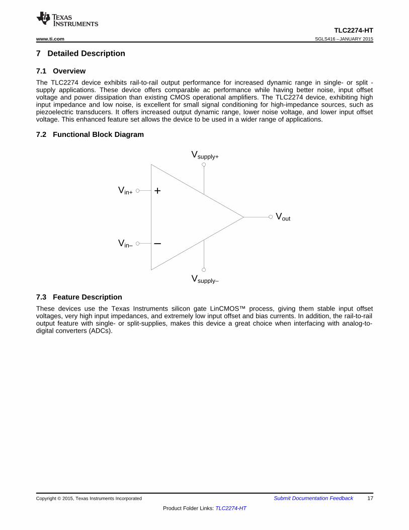
Vin+
Vin±
Vsupply+
Vsupply±
Vout
+
±
TLC2274-HTwww.ti.com SGLS416 –JANUARY 2015
7 Detailed Description
7.1 OverviewThe TLC2274 device exhibits rail-to-rail output performance for increased dynamic range in single- or split -supply applications. These device offers comparable ac performance while having better noise, input offsetvoltage and power dissipation than existing CMOS operational amplifiers. The TLC2274 device, exhibiting highinput impedance and low noise, is excellent for small signal conditioning for high-impedance sources, such aspiezoelectric transducers. It offers increased output dynamic range, lower noise voltage, and lower input offsetvoltage. This enhanced feature set allows the device to be used in a wider range of applications.
7.2 Functional Block Diagram
7.3 Feature DescriptionThese devices use the Texas Instruments silicon gate LinCMOS™ process, giving them stable input offsetvoltages, very high input impedances, and extremely low input offset and bias currents. In addition, the rail-to-railoutput feature with single- or split-supplies, makes this device a great choice when interfacing with analog-to-digital converters (ADCs).
Copyright © 2015, Texas Instruments Incorporated Submit Documentation Feedback 17
Product Folder Links: TLC2274-HT

TLC2274-HTSGLS416 –JANUARY 2015 www.ti.com
8 Application and Implementation
NOTEInformation in the following applications sections is not part of the TI componentspecification, and TI does not warrant its accuracy or completeness. TI’s customers areresponsible for determining suitability of components for their purposes. Customers shouldvalidate and test their design implementation to confirm system functionality.
8.1 Application Information
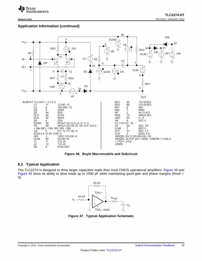
8.1.1 Macromodel InformationMacromodel information provided was derived using Microsim Parts, the model generation software used withMicrosim PSpice. The Boyle macromodel (1) and subcircuit in Figure 46 are generated using the TLC227x typicalelectrical and operating characteristics at TA = 25°C. Using this information, output simulations of the followingkey parameters can be generated to a tolerance of 20% (in most cases):• Maximum positive output voltage swing• Maximum negative output voltage swing• Slew rate• Quiescent power dissipation• Input bias current• Open-loop voltage amplification• Unity-gain frequency• Common-mode rejection ratio• Phase margin• DC output resistance• AC output resistance• Short-circuit output current limit
(1) G. R. Boyle, B. M. Cohn, D. O. Pederson, and J. E. Solomon, “Macromodeling of Integrated Circuit Operational Amplifiers”, IEEEJournal of Solid-State Circuits, SC-9, 353 (1974).
18 Submit Documentation Feedback Copyright © 2015, Texas Instruments Incorporated
Product Folder Links: TLC2274-HT
50 kΩ
50 kΩ
VDD−/GND
VDD+
Rnull
CL
VI
+
−
OUT
+
−
+
−
+
−
+
−
+
−
+
−
+
− +
−
+−
.SUBCKT TLC227x 1 2 3 4 5C1 11 1214E−12C2 6 760.00E−12DC 5 53DXDE 54 5DXDLP 90 91DXDLN 92 90DXDP 4 3DXEGND 99 0POLY (2) (3,0) (4,) 0 .5 .5FB 99 0POLY (5) VB VC VE VLP VLN 0+ 984.9E3 −1E6 1E6 1E6 −1E6GA 6 011 12 377.0E−6GCM 0 6 10 99 134E−9ISS 3 10DC 216.OE−6HLIM 90 0VLIM 1KJ1 11 210 JXJ2 12 110 JXR2 6 9100.OE3
RD1 60 112.653E3RD2 60 122.653E3R01 8 550R02 7 9950RP 3 44.310E3RSS 10 99925.9E3VAD 60 4−.5VB 9 0DC 0VC 3 53 DC .78VE 54 4DC .78VLIM 7 8DC 0VLP 91 0DC 1.9VLN 0 92DC 9.4.MODEL DX D (IS=800.0E−18).MODEL JX PJF (IS=1.500E−12BETA=1.316E-3+ VTO=−.270).ENDS
VCC+
RP
IN −2
IN+
1
VCC−
VAD
RD1
11
J1 J2
10
RSS ISS
3
12
RD2
60
VE
54DE
DP
VC
DC
4
C1
53
R2
6
9
EGND
VB
FB
C2
GCM GAVLIM
8
5
RO1
RO2
HLIM
90
DIP
91
DIN
92
VINVIP
99
7
TLC2274-HTwww.ti.com SGLS416 –JANUARY 2015
Application Information (continued)
Figure 46. Boyle Macromodels and Subcircuit
8.2 Typical ApplicationThe TLC2274 is designed to drive larger capacitive loads than most CMOS operational amplifiers. Figure 48 andFigure 49 show its ability to drive loads up to 1000 pF while maintaining good gain and phase margins (Rnull =0).
Figure 47. Typical Application Schematic
Copyright © 2015, Texas Instruments Incorporated Submit Documentation Feedback 19
Product Folder Links: TLC2274-HT

10
om
−P
hase M
arg
in
10000
CL − Load Capacitance − pF
φm
1000100
VDD = ±5 V
TA = 25°C
Rnull = 20 Ω
Rnull = 10 Ω
Rnull = 0
75°
60°
45°
30°
15°
0°
10 kΩ
10 kΩ
VDD −
VDD +Rnull
CL
VI
Rnull = 100 Ω
Rnull = 50 Ω
3
010
Gain
Marg
in−
dB
6
9
10000CL − Load Capacitance − pF
12
15
1000100
VDD = 5 V
AV = 1
RL = 10 kΩ
TA = 25°C
TLC2274-HTSGLS416 –JANUARY 2015 www.ti.com
Typical Application (continued)8.2.1 Design RequirementsAs per Equation 1:
Table 2. Design ParametersImprovement in Phase Margin UGBW (kHz) R null (Ω) CL (pF)
0 1000 0 10007.15 1000 20 100017.43 1000 50 100032.12 1000 100 1000
8.2.2 Detailed Design ProcedureA smaller series resistor (Rnull) at the output of the device (see Figure 47) improves the gain and phase marginswhen driving large capacitive loads. Figure 48 and Figure 49 show the effects of adding series resistances of 10Ω, 50 Ω, 100 Ω, 200 Ω, and 500 Ω. The addition of this series resistor has two effects: the first is that it adds azero to the transfer function and the second is that it reduces the frequency of the pole associated with theoutput load in the transfer function.
The zero introduced to the transfer function is equal to the series resistance times the load capacitance. Tocalculate the improvement in phase margin, Equation 1 can be used.
Δφm1 = tan–1 (2 × π × UGBW × Rnull × CL)
where• Δφm1 = Improvement in phase margin• UGBW = Unity-gain bandwidth frequency• Rnull = Output series resistance• CL = Load capacitance (1)
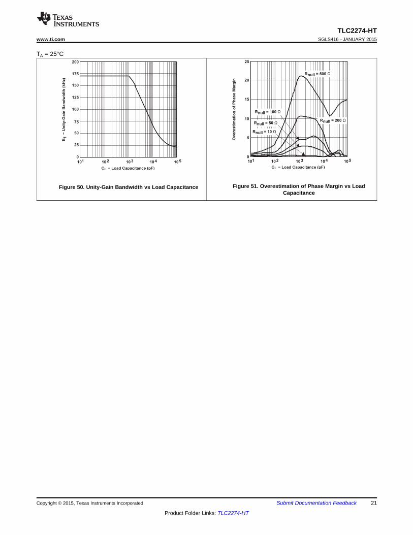
The unity-gain bandwidth (UGBW) frequency decreases as the capacitive load increases (see Figure 47). To useequation 1, UGBW must be approximated from Figure 47. Using Equation 1 alone overestimates theimprovement in phase margin, as illustrated in Figure 51. The overestimation is caused by the decrease in thefrequency of the pole associated with the load, thus providing additional phase shift and reducing the overallimprovement in phase margin. Using Figure 47, with Equation 1 enables the designer to choose the appropriateoutput series resistance to optimize the design of circuits driving large capacitance loads.
8.2.3 Application CurvesTA = 25°C
Figure 49. Gain Margin vs Load CapacitanceFigure 48. Phase Margin vs Load Capacitance
20 Submit Documentation Feedback Copyright © 2015, Texas Instruments Incorporated
Product Folder Links: TLC2274-HT
−U
nit
y-G
ain
Ban
dw
idth
(kH
z)
CL − Load Capacitance (pF)
B1
150
25
100
0
200
125
175
50
75
101 102 103 104 105
Overe
sti
mati
on
of
Ph
ase
Marg
in
CL − Load Capacitance (pF)
15
10
5
0
20
25
101 102 103 104 105
Rnull = 100 Ω
Rnull = 50 Ω
Rnull = 10 Ω
Rnull = 500 Ω
Rnull = 200 Ω
TLC2274-HTwww.ti.com SGLS416 –JANUARY 2015
TA = 25°C
Figure 51. Overestimation of Phase Margin vs LoadFigure 50. Unity-Gain Bandwidth vs Load CapacitanceCapacitance
Copyright © 2015, Texas Instruments Incorporated Submit Documentation Feedback 21
Product Folder Links: TLC2274-HT
TLC2274-HTSGLS416 –JANUARY 2015 www.ti.com
9 Power Supply RecommendationsTLC2274 operates from ±2.2- to ±8-V. In addition, key parameters are assured over the specified temperaturerange, –55°C to 125°C. Parameters which vary significantly with operating voltage or temperature are shown inthe Typical Characteristics.
10 Layout
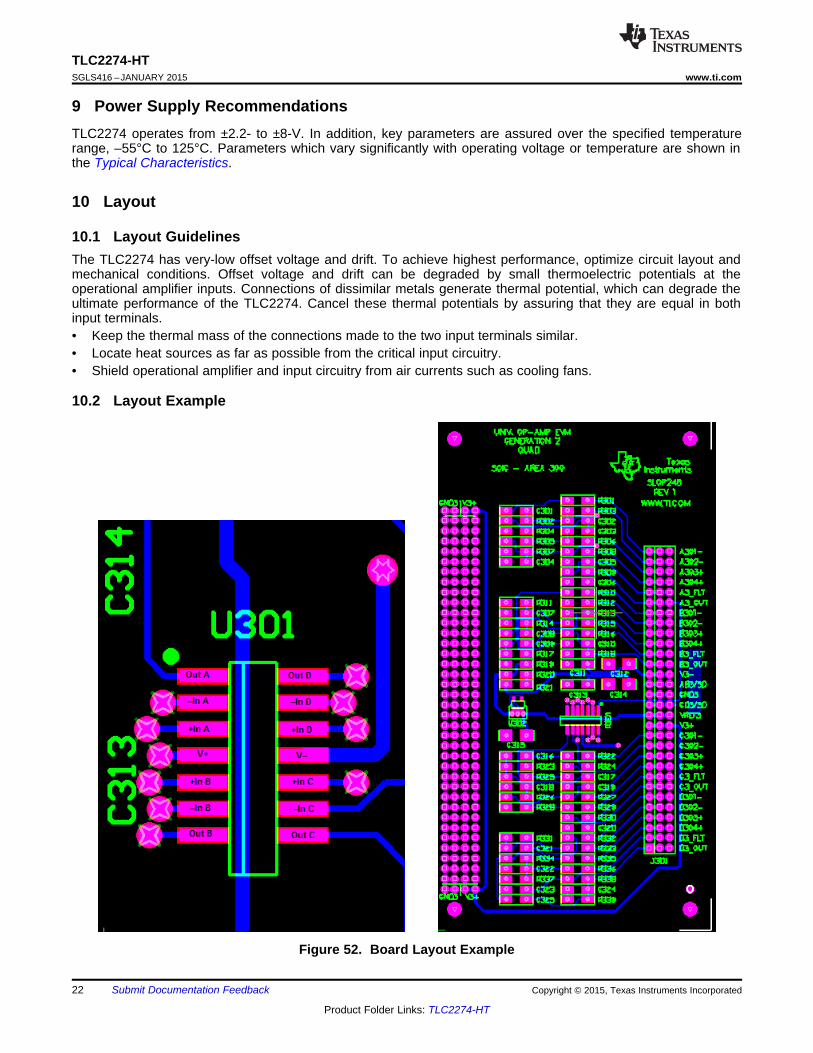
10.1 Layout GuidelinesThe TLC2274 has very-low offset voltage and drift. To achieve highest performance, optimize circuit layout andmechanical conditions. Offset voltage and drift can be degraded by small thermoelectric potentials at theoperational amplifier inputs. Connections of dissimilar metals generate thermal potential, which can degrade theultimate performance of the TLC2274. Cancel these thermal potentials by assuring that they are equal in bothinput terminals.• Keep the thermal mass of the connections made to the two input terminals similar.• Locate heat sources as far as possible from the critical input circuitry.• Shield operational amplifier and input circuitry from air currents such as cooling fans.
10.2 Layout Example
Figure 52. Board Layout Example
22 Submit Documentation Feedback Copyright © 2015, Texas Instruments Incorporated
Product Folder Links: TLC2274-HT

TLC2274-HTwww.ti.com SGLS416 –JANUARY 2015
11 Device and Documentation Support
11.1 TrademarksLinCMOS is a trademark of Texas Instruments.All other trademarks are the property of their respective owners.
11.2 Electrostatic Discharge CautionThese devices have limited built-in ESD protection. The leads should be shorted together or the device placed in conductive foamduring storage or handling to prevent electrostatic damage to the MOS gates.
11.3 GlossarySLYZ022 — TI Glossary.
This glossary lists and explains terms, acronyms, and definitions.
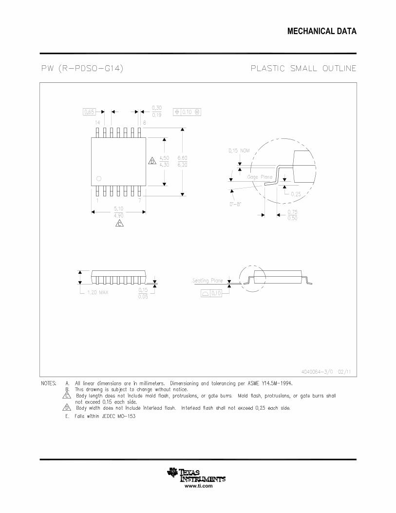
12 Mechanical, Packaging, and Orderable InformationThe following pages include mechanical, packaging, and orderable information. This information is the mostcurrent data available for the designated devices. This data is subject to change without notice and revision ofthis document. For browser-based versions of this data sheet, refer to the left-hand navigation.
Copyright © 2015, Texas Instruments Incorporated Submit Documentation Feedback 23
Product Folder Links: TLC2274-HT
PACKAGE OPTION ADDENDUM
www.ti.com 16-Jun-2015
Addendum-Page 1
PACKAGING INFORMATION
Orderable Device Status(1)
Package Type PackageDrawing
Pins PackageQty
Eco Plan(2)
Lead/Ball Finish(6)
MSL Peak Temp(3)
Op Temp (°C) Device Marking(4/5)
Samples
TLC2274EPWRQ1 ACTIVE TSSOP PW 14 2000 Green (RoHS& no Sb/Br)
CU NIPDAU Level-2-260C-1 YEAR -40 to 150 2274EQ1
(1) The marketing status values are defined as follows:ACTIVE: Product device recommended for new designs.LIFEBUY: TI has announced that the device will be discontinued, and a lifetime-buy period is in effect.NRND: Not recommended for new designs. Device is in production to support existing customers, but TI does not recommend using this part in a new design.PREVIEW: Device has been announced but is not in production. Samples may or may not be available.OBSOLETE: TI has discontinued the production of the device.
(2) Eco Plan - The planned eco-friendly classification: Pb-Free (RoHS), Pb-Free (RoHS Exempt), or Green (RoHS & no Sb/Br) - please check http://www.ti.com/productcontent for the latest availabilityinformation and additional product content details.TBD: The Pb-Free/Green conversion plan has not been defined.Pb-Free (RoHS): TI's terms "Lead-Free" or "Pb-Free" mean semiconductor products that are compatible with the current RoHS requirements for all 6 substances, including the requirement thatlead not exceed 0.1% by weight in homogeneous materials. Where designed to be soldered at high temperatures, TI Pb-Free products are suitable for use in specified lead-free processes.Pb-Free (RoHS Exempt): This component has a RoHS exemption for either 1) lead-based flip-chip solder bumps used between the die and package, or 2) lead-based die adhesive used betweenthe die and leadframe. The component is otherwise considered Pb-Free (RoHS compatible) as defined above.Green (RoHS & no Sb/Br): TI defines "Green" to mean Pb-Free (RoHS compatible), and free of Bromine (Br) and Antimony (Sb) based flame retardants (Br or Sb do not exceed 0.1% by weightin homogeneous material)
(3) MSL, Peak Temp. - The Moisture Sensitivity Level rating according to the JEDEC industry standard classifications, and peak solder temperature.
(4) There may be additional marking, which relates to the logo, the lot trace code information, or the environmental category on the device.
(5) Multiple Device Markings will be inside parentheses. Only one Device Marking contained in parentheses and separated by a "~" will appear on a device. If a line is indented then it is a continuationof the previous line and the two combined represent the entire Device Marking for that device.
(6) Lead/Ball Finish - Orderable Devices may have multiple material finish options. Finish options are separated by a vertical ruled line. Lead/Ball Finish values may wrap to two lines if the finishvalue exceeds the maximum column width.
Important Information and Disclaimer:The information provided on this page represents TI's knowledge and belief as of the date that it is provided. TI bases its knowledge and belief on informationprovided by third parties, and makes no representation or warranty as to the accuracy of such information. Efforts are underway to better integrate information from third parties. TI has taken andcontinues to take reasonable steps to provide representative and accurate information but may not have conducted destructive testing or chemical analysis on incoming materials and chemicals.TI and TI suppliers consider certain information to be proprietary, and thus CAS numbers and other limited information may not be available for release.
In no event shall TI's liability arising out of such information exceed the total purchase price of the TI part(s) at issue in this document sold by TI to Customer on an annual basis.
PACKAGE OPTION ADDENDUM
www.ti.com 16-Jun-2015
Addendum-Page 2
OTHER QUALIFIED VERSIONS OF TLC2274-HT :
• Catalog: TLC2274
• Automotive: TLC2274-Q1
• Enhanced Product: TLC2274-EP
• Military: TLC2274M
NOTE: Qualified Version Definitions:
• Catalog - TI's standard catalog product
• Automotive - Q100 devices qualified for high-reliability automotive applications targeting zero defects
• Enhanced Product - Supports Defense, Aerospace and Medical Applications
• Military - QML certified for Military and Defense Applications
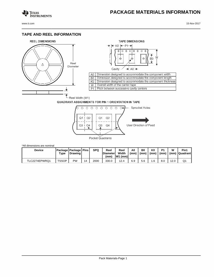
TAPE AND REEL INFORMATION
*All dimensions are nominal
Device PackageType
PackageDrawing
Pins SPQ ReelDiameter
(mm)
ReelWidth
W1 (mm)
A0(mm)
B0(mm)
K0(mm)
P1(mm)
W(mm)
Pin1Quadrant
TLC2274EPWRQ1 TSSOP PW 14 2000 330.0 12.4 6.9 5.6 1.6 8.0 12.0 Q1
PACKAGE MATERIALS INFORMATION
www.ti.com 15-Nov-2017
Pack Materials-Page 1
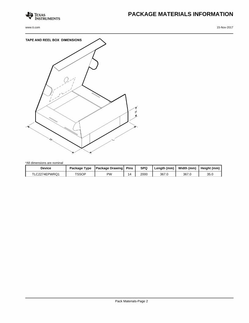
*All dimensions are nominal
Device Package Type Package Drawing Pins SPQ Length (mm) Width (mm) Height (mm)
TLC2274EPWRQ1 TSSOP PW 14 2000 367.0 367.0 35.0
PACKAGE MATERIALS INFORMATION
www.ti.com 15-Nov-2017
Pack Materials-Page 2
IMPORTANT NOTICE
Texas Instruments Incorporated (TI) reserves the right to make corrections, enhancements, improvements and other changes to itssemiconductor products and services per JESD46, latest issue, and to discontinue any product or service per JESD48, latest issue. Buyersshould obtain the latest relevant information before placing orders and should verify that such information is current and complete.TI’s published terms of sale for semiconductor products (http://www.ti.com/sc/docs/stdterms.htm) apply to the sale of packaged integratedcircuit products that TI has qualified and released to market. Additional terms may apply to the use or sale of other types of TI products andservices.Reproduction of significant portions of TI information in TI data sheets is permissible only if reproduction is without alteration and isaccompanied by all associated warranties, conditions, limitations, and notices. TI is not responsible or liable for such reproduceddocumentation. Information of third parties may be subject to additional restrictions. Resale of TI products or services with statementsdifferent from or beyond the parameters stated by TI for that product or service voids all express and any implied warranties for theassociated TI product or service and is an unfair and deceptive business practice. TI is not responsible or liable for any such statements.Buyers and others who are developing systems that incorporate TI products (collectively, “Designers”) understand and agree that Designersremain responsible for using their independent analysis, evaluation and judgment in designing their applications and that Designers havefull and exclusive responsibility to assure the safety of Designers' applications and compliance of their applications (and of all TI productsused in or for Designers’ applications) with all applicable regulations, laws and other applicable requirements. Designer represents that, withrespect to their applications, Designer has all the necessary expertise to create and implement safeguards that (1) anticipate dangerousconsequences of failures, (2) monitor failures and their consequences, and (3) lessen the likelihood of failures that might cause harm andtake appropriate actions. Designer agrees that prior to using or distributing any applications that include TI products, Designer willthoroughly test such applications and the functionality of such TI products as used in such applications.TI’s provision of technical, application or other design advice, quality characterization, reliability data or other services or information,including, but not limited to, reference designs and materials relating to evaluation modules, (collectively, “TI Resources”) are intended toassist designers who are developing applications that incorporate TI products; by downloading, accessing or using TI Resources in anyway, Designer (individually or, if Designer is acting on behalf of a company, Designer’s company) agrees to use any particular TI Resourcesolely for this purpose and subject to the terms of this Notice.TI’s provision of TI Resources does not expand or otherwise alter TI’s applicable published warranties or warranty disclaimers for TIproducts, and no additional obligations or liabilities arise from TI providing such TI Resources. TI reserves the right to make corrections,enhancements, improvements and other changes to its TI Resources. TI has not conducted any testing other than that specificallydescribed in the published documentation for a particular TI Resource.Designer is authorized to use, copy and modify any individual TI Resource only in connection with the development of applications thatinclude the TI product(s) identified in such TI Resource. NO OTHER LICENSE, EXPRESS OR IMPLIED, BY ESTOPPEL OR OTHERWISETO ANY OTHER TI INTELLECTUAL PROPERTY RIGHT, AND NO LICENSE TO ANY TECHNOLOGY OR INTELLECTUAL PROPERTYRIGHT OF TI OR ANY THIRD PARTY IS GRANTED HEREIN, including but not limited to any patent right, copyright, mask work right, orother intellectual property right relating to any combination, machine, or process in which TI products or services are used. Informationregarding or referencing third-party products or services does not constitute a license to use such products or services, or a warranty orendorsement thereof. Use of TI Resources may require a license from a third party under the patents or other intellectual property of thethird party, or a license from TI under the patents or other intellectual property of TI.TI RESOURCES ARE PROVIDED “AS IS” AND WITH ALL FAULTS. TI DISCLAIMS ALL OTHER WARRANTIES ORREPRESENTATIONS, EXPRESS OR IMPLIED, REGARDING RESOURCES OR USE THEREOF, INCLUDING BUT NOT LIMITED TOACCURACY OR COMPLETENESS, TITLE, ANY EPIDEMIC FAILURE WARRANTY AND ANY IMPLIED WARRANTIES OFMERCHANTABILITY, FITNESS FOR A PARTICULAR PURPOSE, AND NON-INFRINGEMENT OF ANY THIRD PARTY INTELLECTUALPROPERTY RIGHTS. TI SHALL NOT BE LIABLE FOR AND SHALL NOT DEFEND OR INDEMNIFY DESIGNER AGAINST ANY CLAIM,INCLUDING BUT NOT LIMITED TO ANY INFRINGEMENT CLAIM THAT RELATES TO OR IS BASED ON ANY COMBINATION OFPRODUCTS EVEN IF DESCRIBED IN TI RESOURCES OR OTHERWISE. IN NO EVENT SHALL TI BE LIABLE FOR ANY ACTUAL,DIRECT, SPECIAL, COLLATERAL, INDIRECT, PUNITIVE, INCIDENTAL, CONSEQUENTIAL OR EXEMPLARY DAMAGES INCONNECTION WITH OR ARISING OUT OF TI RESOURCES OR USE THEREOF, AND REGARDLESS OF WHETHER TI HAS BEENADVISED OF THE POSSIBILITY OF SUCH DAMAGES.Unless TI has explicitly designated an individual product as meeting the requirements of a particular industry standard (e.g., ISO/TS 16949and ISO 26262), TI is not responsible for any failure to meet such industry standard requirements.Where TI specifically promotes products as facilitating functional safety or as compliant with industry functional safety standards, suchproducts are intended to help enable customers to design and create their own applications that meet applicable functional safety standardsand requirements. Using products in an application does not by itself establish any safety features in the application. Designers mustensure compliance with safety-related requirements and standards applicable to their applications. Designer may not use any TI products inlife-critical medical equipment unless authorized officers of the parties have executed a special contract specifically governing such use.Life-critical medical equipment is medical equipment where failure of such equipment would cause serious bodily injury or death (e.g., lifesupport, pacemakers, defibrillators, heart pumps, neurostimulators, and implantables). Such equipment includes, without limitation, allmedical devices identified by the U.S. Food and Drug Administration as Class III devices and equivalent classifications outside the U.S.TI may expressly designate certain products as completing a particular qualification (e.g., Q100, Military Grade, or Enhanced Product).Designers agree that it has the necessary expertise to select the product with the appropriate qualification designation for their applicationsand that proper product selection is at Designers’ own risk. Designers are solely responsible for compliance with all legal and regulatoryrequirements in connection with such selection.Designer will fully indemnify TI and its representatives against any damages, costs, losses, and/or liabilities arising out of Designer’s non-compliance with the terms and provisions of this Notice.
Mailing Address: Texas Instruments, Post Office Box 655303, Dallas, Texas 75265Copyright © 2017, Texas Instruments Incorporated


![LinCMOS Programmable Low-Power Operational ......Title LinCMOS Programmable Low-Power Operational Amplifiers (Rev. D) Author Texas Instruments, Incorporated [SLOS090,D ]](https://img.dokumen.tips/doc/110x75/60c520663ed5937ead0851c0/lincmos-programmable-low-power-operational-title-lincmos-programmable-low-power.jpg)