Embed Size (px)
Citation preview

www.ti.com
FEATURES
1
2
3
4
8
7
6
5
1OUT
1IN-
1IN+
GND
VCC
2OUT
2IN-
2IN+
D PACKAGE
(TOP VIEW)
OUT
IN+
SYMBOL (each comparator)
IN -
DESCRIPTION/ORDERING INFORMATION
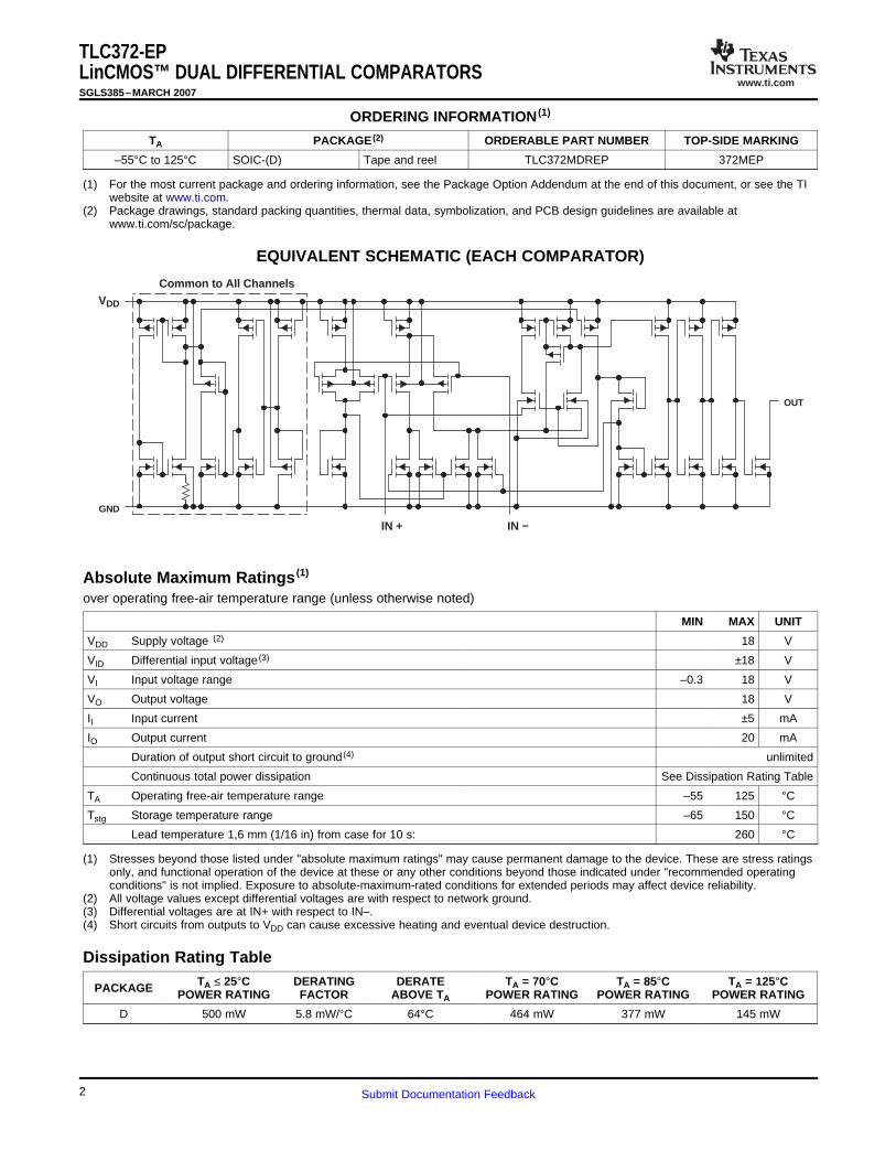
TLC372-EPLinCMOS™ DUAL DIFFERENTIAL COMPARATORS
SGLS385–MARCH 2007
• Controlled Baseline • Common-Mode Input Voltage Range IncludesGround– One Assembly/Test Site, One Fabrication
Site • Output Compatible With TTL, MOS, and CMOS• Extended Temperature Performance of –55°C • Pin-Compatible With LM393
to 125°C• Enhanced Diminishing Manufacturing Sources
(DMS) Support• Enhanced Product Change Notification• Qualification Pedigree (1)
• ESD Protection Exceeds 2000 V PerMIL-STD-883, Method 3015; Exceeds 100 VUsing Machine Model (C = 200 pF, R = 0)
• Single or Dual-Supply Operation• Wide Range of Supply Voltages . . .4 V to 18 V• Very Low Supply Current Drain . . .150 µA Typ
at 5 V• Fast Response Time . . . 200 ns Typ for
TTL-Level Input Step• Built-in ESD Protection• High Input Impedance . . . 1012Ω Typ• Extremely Low Input Bias Current. . .5 pA Typ• Ultrastable Low Input Offset Voltage• Input Offset Voltage Change at Worst-Case
Input Conditions Typically 0.23 µV/Month,Including the First 30 Days
(1) Component qualification in accordance with JEDEC andindustry standards to ensure reliable operation over anextended temperature range. This includes, but is not limitedto, Highly Accelerated Stress Test (HAST) or biased 85/85,temperature cycle, autoclave or unbiased HAST,electromigration, bond intermetallic life, and mold compoundlife. Such qualification testing should not be viewed asjustifying use of this component beyond specifiedperformance and environmental limits.
This device is fabricated using LinCMOS™ technology and consists of two independent voltage comparators,each designed to operate from a single power supply. Operation from dual supplies is also possible if thedifference between the two supplies is 4 V to 18 V. Each device features extremely high input impedance(typically greater than 1012Ω), allowing direct interfacing with high-impedance sources. The outputs aren-channel open-drain configurations and can be connected to achieve positive-logic wired-AND relationships.
The TLC372 has internal electrostatic discharge (ESD) protection circuits and has been classified with a 2000-VESD rating using human-body-model (HBM) testing. However, care should be exercised in handling this deviceas exposure to ESD may result in a degradation of the device parametric performance.
The TLC372 is characterized for operation from –55°C to 125°C.
Please be aware that an important notice concerning availability, standard warranty, and use in critical applications of TexasInstruments semiconductor products and disclaimers thereto appears at the end of this data sheet.
LinCMOS is a trademark of Texas Instruments.
PRODUCTION DATA information is current as of publication date. Copyright © 2007, Texas Instruments IncorporatedProducts conform to specifications per the terms of the TexasInstruments standard warranty. Production processing does notnecessarily include testing of all parameters.
www.ti.com
EQUIVALENT SCHEMATIC (EACH COMPARATOR)
Common to All ChannelsVDD
GND
OUT
IN + IN −
Absolute Maximum Ratings (1)
Dissipation Rating Table
TLC372-EPLinCMOS™ DUAL DIFFERENTIAL COMPARATORSSGLS385–MARCH 2007
ORDERING INFORMATION (1)
TA PACKAGE (2) ORDERABLE PART NUMBER TOP-SIDE MARKING
–55°C to 125°C SOIC-(D) Tape and reel TLC372MDREP 372MEP
(1) For the most current package and ordering information, see the Package Option Addendum at the end of this document, or see the TIwebsite at www.ti.com.
(2) Package drawings, standard packing quantities, thermal data, symbolization, and PCB design guidelines are available atwww.ti.com/sc/package.
over operating free-air temperature range (unless otherwise noted)
MIN MAX UNIT
VDD Supply voltage (2) 18 V
VID Differential input voltage (3) ±18 V
VI Input voltage range –0.3 18 V
VO Output voltage 18 V
II Input current ±5 mA
IO Output current 20 mA
Duration of output short circuit to ground (4) unlimited
Continuous total power dissipation See Dissipation Rating Table
TA Operating free-air temperature range –55 125 °C
Tstg Storage temperature range –65 150 °C
Lead temperature 1,6 mm (1/16 in) from case for 10 s: 260 °C
(1) Stresses beyond those listed under "absolute maximum ratings" may cause permanent damage to the device. These are stress ratingsonly, and functional operation of the device at these or any other conditions beyond those indicated under "recommended operatingconditions" is not implied. Exposure to absolute-maximum-rated conditions for extended periods may affect device reliability.
(2) All voltage values except differential voltages are with respect to network ground.(3) Differential voltages are at IN+ with respect to IN–.(4) Short circuits from outputs to VDD can cause excessive heating and eventual device destruction.
TA ≤ 25°C DERATING DERATE TA = 70°C TA = 85°C TA = 125°CPACKAGE POWER RATING FACTOR ABOVE TA POWER RATING POWER RATING POWER RATING
D 500 mW 5.8 mW/°C 64°C 464 mW 377 mW 145 mW
2 Submit Documentation Feedback
www.ti.com
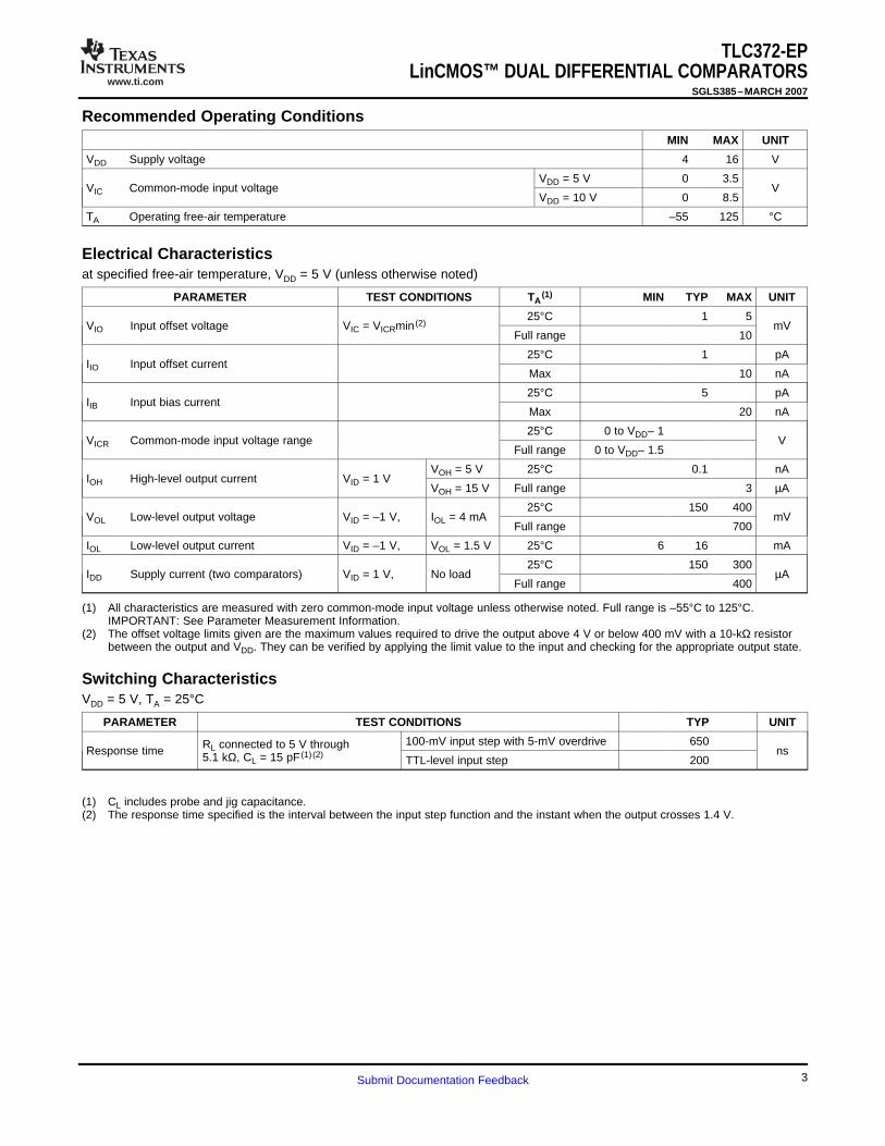
Recommended Operating Conditions
Electrical Characteristics
Switching Characteristics
TLC372-EPLinCMOS™ DUAL DIFFERENTIAL COMPARATORS
SGLS385–MARCH 2007
MIN MAX UNIT
VDD Supply voltage 4 16 V
VDD = 5 V 0 3.5VIC Common-mode input voltage V
VDD = 10 V 0 8.5
TA Operating free-air temperature –55 125 °C
at specified free-air temperature, VDD = 5 V (unless otherwise noted)
PARAMETER TEST CONDITIONS TA(1) MIN TYP MAX UNIT
25°C 1 5VIO Input offset voltage VIC = VICRmin (2) mV
Full range 10
25°C 1 pAIIO Input offset current
Max 10 nA
25°C 5 pAIIB Input bias current
Max 20 nA
25°C 0 to VDD– 1VICR Common-mode input voltage range V
Full range 0 to VDD– 1.5
VOH = 5 V 25°C 0.1 nAIOH High-level output current VID = 1 V
VOH = 15 V Full range 3 µA
25°C 150 400VOL Low-level output voltage VID = –1 V, IOL = 4 mA mV
Full range 700
IOL Low-level output current VID = –1 V, VOL = 1.5 V 25°C 6 16 mA
25°C 150 300IDD Supply current (two comparators) VID = 1 V, No load µA
Full range 400
(1) All characteristics are measured with zero common-mode input voltage unless otherwise noted. Full range is –55°C to 125°C.IMPORTANT: See Parameter Measurement Information.
(2) The offset voltage limits given are the maximum values required to drive the output above 4 V or below 400 mV with a 10-kΩ resistorbetween the output and VDD. They can be verified by applying the limit value to the input and checking for the appropriate output state.
VDD = 5 V, TA = 25°C
PARAMETER TEST CONDITIONS TYP UNIT
100-mV input step with 5-mV overdrive 650RL connected to 5 V throughResponse time ns5.1 kΩ, CL = 15 pF (1) (2) TTL-level input step 200
(1) CL includes probe and jig capacitance.(2) The response time specified is the interval between the input step function and the instant when the output crosses 1.4 V.
3Submit Documentation Feedback

www.ti.com
PARAMETER MEASUREMENT INFORMATION
5 V
5.1 kΩ
VO
Applied V IOLimit
VO
5.1 kΩ
1 V
−4 V
−
+
−
+
(a) VIO WITH VIC = 0 (b) VIO WITH VIC = 4 V
Applied V IOLimit
TLC372-EPLinCMOS™ DUAL DIFFERENTIAL COMPARATORSSGLS385–MARCH 2007
The digital output stage of the TLC372 can be damaged if it is held in the linear region of the transfer curve.Conventional operational amplifier/comparator testing incorporates the use of a servo loop that is designed toforce the device output to a level within this linear region. Since the servo-loop method of testing cannot beused, the following alternatives for measuring parameters such as input offset voltage, common-mode rejection,etc., are offered.
To verify that the input offset voltage falls within the limits specified, the limit value is applied to the input asshown in Figure 1(a). With the noninverting input positive with respect to the inverting input, the output should behigh. With the input polarity reversed, the output should be low.
A similar test can be made to verify the input offset voltage at the common-mode extremes. The supply voltagescan be slewed as shown in Figure 1(b) for the VICR test, rather than changing the input voltages, to providegreater accuracy.
Figure 1. Method for Verifying That Input Offset Voltage is Within Specified Limits
A close approximation of the input offset voltage can be obtained by using a binary search method to vary thedifferential input voltage while monitoring the output state. When the applied input voltage differential is equal,but opposite in polarity, to the input offset voltage, the output changes states.
4 Submit Documentation Feedback
www.ti.com
R65.1 kΩBuffer
U1b1/4 TLC274C
R1240 kΩ
C21 µF
R447 kΩ
U1a1/4 TLC274CN
U1c1/4 TLC274CN
R210 kΩR3
100 kΩ
C10.1 µF
R10100 kΩ, 1%
R910 kΩ, 1%
R71 MΩ
R81.8 kΩ, 1%
R51.8 kΩ, 1%
VDD
DUT
Integrator
VIO(X100)
C30.68 µF
C40.1 µF
TriangleGenerator
−
+
−
+
−
+
TLC372-EPLinCMOS™ DUAL DIFFERENTIAL COMPARATORS
SGLS385–MARCH 2007
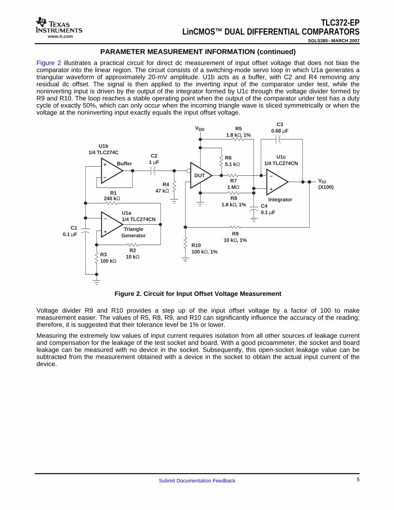
PARAMETER MEASUREMENT INFORMATION (continued)
Figure 2 illustrates a practical circuit for direct dc measurement of input offset voltage that does not bias thecomparator into the linear region. The circuit consists of a switching-mode servo loop in which U1a generates atriangular waveform of approximately 20-mV amplitude. U1b acts as a buffer, with C2 and R4 removing anyresidual dc offset. The signal is then applied to the inverting input of the comparator under test, while thenoninverting input is driven by the output of the integrator formed by U1c through the voltage divider formed byR9 and R10. The loop reaches a stable operating point when the output of the comparator under test has a dutycycle of exactly 50%, which can only occur when the incoming triangle wave is sliced symmetrically or when thevoltage at the noninverting input exactly equals the input offset voltage.
Figure 2. Circuit for Input Offset Voltage Measurement
Voltage divider R9 and R10 provides a step up of the input offset voltage by a factor of 100 to makemeasurement easier. The values of R5, R8, R9, and R10 can significantly influence the accuracy of the reading;therefore, it is suggested that their tolerance level be 1% or lower.
Measuring the extremely low values of input current requires isolation from all other sources of leakage currentand compensation for the leakage of the test socket and board. With a good picoammeter, the socket and boardleakage can be measured with no device in the socket. Subsequently, this open-socket leakage value can besubtracted from the measurement obtained with a device in the socket to obtain the actual input current of thedevice.
5Submit Documentation Feedback
www.ti.com
Low-to-High-
Level Output
DUT
5.1 kΩ 1 µF
0.1 µF
1 kΩ
50 Ω
CL(see Note A)
VDD
Pulse
Generator
Input Offset Voltage
Compensation Adjustment10 Ω
10 Turn
1 V
- 1 V
Overdrive
Input
100 mV
Overdrive
Input
tf
tPHL
10%
50%
90%90%
50%
tr
tPLH
High-to-Low-
Level Output
TEST CIRCUIT
VOLTAGE WAVEFORMS
10%
100 mV
NOTE: A. C includes probe and jig capacitanceL
TLC372-EPLinCMOS™ DUAL DIFFERENTIAL COMPARATORSSGLS385–MARCH 2007
PARAMETER MEASUREMENT INFORMATION (continued)
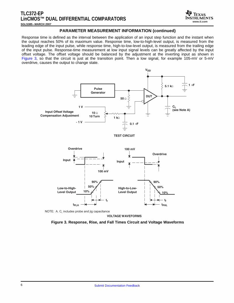
Response time is defined as the interval between the application of an input step function and the instant whenthe output reaches 50% of its maximum value. Response time, low-to-high-level output, is measured from theleading edge of the input pulse, while response time, high-to-low-level output, is measured from the trailing edgeof the input pulse. Response-time measurement at low input signal levels can be greatly affected by the inputoffset voltage. The offset voltage should be balanced by the adjustment at the inverting input as shown inFigure 3, so that the circuit is just at the transition point. Then a low signal, for example 105-mV or 5-mVoverdrive, causes the output to change state.
Figure 3. Response, Rise, and Fall Times Circuit and Voltage Waveforms
6 Submit Documentation Feedback

www.ti.com
PRINCIPLES OF OPERATION
LinCMOS™ Process
Electrostatic Discharge (ESD)
D3
R2
Q2
To Protected Circuit
VDD
D2D1
Q1
R1Input
VSS
Input Protection Circuit Operation
TLC372-EPLinCMOS™ DUAL DIFFERENTIAL COMPARATORS
SGLS385–MARCH 2007
The LinCMOS process is a linear polysilicon-gate complementary-MOS process. Primarily designed forsingle-supply applications, LinCMOS products facilitate the design of a wide range of high-performance analogfunctions, from operational amplifiers to complex mixed-mode converters.
This short guide is intended to answer the most frequently asked questions related to the quality and reliability ofLinCMOS products. Further questions should be directed to the nearest TI field sales office.
CMOS circuits are prone to gate oxide breakdown when exposed to high voltages even if the exposure is onlyfor very short periods of time. ESD is one of the most common causes of damage to CMOS devices. It canoccur when a device is handled without proper consideration for environmental electrostatic charges, e.g. duringboard assembly. If a circuit in which one amplifier from a dual operational amplifier is being used and the unusedpins are left open, high voltages tends to develop. If there is no provision for ESD protection, these voltages mayeventually punch through the gate oxide and cause the device to fail. To prevent voltage buildup, each pin isprotected by internal circuitry.
Standard ESD-protection circuits safely shunt the ESD current by providing a mechanism whereby one or moretransistors break down at voltages higher than the normal operating voltages but lower than the breakdownvoltage of the input gate. This type of protection scheme is limited by leakage currents which flow through theshunting transistors during normal operation after an ESD voltage has occurred. Although these currents aresmall, on the order of tens of nanoamps, CMOS amplifiers are often specified to draw input currents as low astens of picoamps.
To overcome this limitation, TI design engineers developed the patented ESD-protection circuit shown inFigure 4. This circuit can withstand several successive 1-kV ESD pulses, while reducing or eliminating leakagecurrents that may be drawn through the input pins. A more detailed discussion of the operation of TI's ESD-protection circuit is presented in Circuit Design Consideration.
Figure 4. LinCMOS™ ESD-Protection Schematic
Texas Instruments patented protection circuitry allows for both positive-and negative-going ESD transients.These transients are characterized by extremely fast rise times and usually low energies, and can occur bothwhen the device has all pins open and when it is installed in a circuit.
7Submit Documentation Feedback

www.ti.com
Positive ESD Transients
Negative ESD Transients
Circuit-Design Considerations
TLC372-EPLinCMOS™ DUAL DIFFERENTIAL COMPARATORSSGLS385–MARCH 2007
PRINCIPLES OF OPERATION (continued)
Initial positive charged energy is shunted through Q1 to VSS. Q1 turns on when the voltage at the input risesabove the voltage on the VDD pin by a value equal to the VEB of Q1. The base current increases through R2 withinput current as Q1 saturates. The base current through R2 forces the voltage at the drain and gate of Q2 toexceed its threshold level (VT ~ 22 V to 26 V) and turn Q2 on. The shunted input current through Q1 to VSS isnow shunted through the n-channel enhancement-type MOSFET Q2 to VSS. If the voltage on the input pincontinues to rise, the breakdown voltage of the zener diode D3 is exceeded, and all remaining energy isdissipated in R1 and D3. The breakdown voltage of D3 is designed to be 24 V to 27 V, which is well below thegate oxide voltage of the circuit to be protected.
The negative charged ESD transients are shunted directly through D1. Additional energy is dissipated in R1 andD2 as D2 becomes forward biased. The voltage seen by the protected circuit is –0.3 V to –1 V (the forwardvoltage of D1 and D2).
LinCMOS products are being used in actual circuit environments that have input voltages that exceed therecommended common-mode input voltage range and activate the input protection circuit. Even under normaloperation, these conditions occur during circuit power up or power down, and in many cases, when the device isbeing used for a signal conditioning function. The input voltages can exceed VICR and not damage the deviceonly if the inputs are current limited. The recommended current limit shown on most product data sheets is ± 5mA. Figure 5 and Figure 6 show typical characteristics for input voltage versus input current.
Normal operation and correct output state can be expected even when the input voltage exceeds the positivesupply voltage. Again, the input current should be externally limited even though internal positive current limitingis achieved in the input protection circuit by the action of Q1. When Q1 is on, it saturates and limits the currentto approximately 5-mA collector current by design. When saturated, Q1 base current increases with inputcurrent. This base current is forced into the VDD pin and into the device IDD or the VDD supply through R2producing the current limiting effects shown in Figure 5. This internal limiting lasts only as long as the inputvoltage is below the VT of Q2.
When the input voltage exceeds the negative supply voltage, normal operation is affected and output voltagestates may not be correct. Also, the isolation between channels of multiple devices (duals and quads) can beseverely affected. External current limiting must be used since this current is directly shunted by D1 and D2 andno internal limiting is achieved. If normal output voltage states are required, an external input voltage clamp isrequired (see Figure 7).
8 Submit Documentation Feedback

www.ti.com
VDD0
Inpu
t Cur
rent
− m
A
Input V oltage − V
8
1
2
3
4
5
6
7
VDD + 4 VDD + 8 VDD + 12
TA = 25°C
INPUT CURRENTvs
INPUT VOLTAGE
TA = 25°C
VDD − 0.9VDD − 0.7VDD − 0.5
Input V oltage − V
Inpu
t Cur
rent
− m
A
0VDD − 0.3
1
2
3
4
5
6
7
8
9
10
INPUT CURRENTvs
INPUT VOLTAGE
TLC372-EPLinCMOS™ DUAL DIFFERENTIAL COMPARATORS
SGLS385–MARCH 2007
PRINCIPLES OF OPERATION (continued)
Figure 5.
Figure 6.
9Submit Documentation Feedback

www.ti.com
−
+
Vref
TLC372
RL
VDD
RI
See Note A
VI
Positive V oltage Input Current LImit:
Negative V oltage Input Current LImit:
RI =+VI − VDD − 0.3 V
5 mA
RI =−VI − VDD − (−0.3 V)
5 mA
TLC372-EPLinCMOS™ DUAL DIFFERENTIAL COMPARATORSSGLS385–MARCH 2007
PRINCIPLES OF OPERATION (continued)
A. If the correct output state is required when the negative input exceeds VSS, a Schottky clamp is required.
Figure 7. Typical Input Current-Limiting Configuration for a LinCMOS™ Comparator
10 Submit Documentation Feedback

PACKAGE OPTION ADDENDUM
www.ti.com 31-May-2014
Addendum-Page 1
PACKAGING INFORMATION
Orderable Device Status(1)
Package Type PackageDrawing
Pins PackageQty
Eco Plan(2)
Lead/Ball Finish(6)
MSL Peak Temp(3)
Op Temp (°C) Device Marking(4/5)
Samples
TLC372MDREP ACTIVE SOIC D 8 2500 Green (RoHS& no Sb/Br)
CU NIPDAU Level-1-260C-UNLIM -55 to 125 372MEP
V62/06675-01XE ACTIVE SOIC D 8 2500 Green (RoHS& no Sb/Br)
CU NIPDAU Level-1-260C-UNLIM -55 to 125 372MEP
(1) The marketing status values are defined as follows:ACTIVE: Product device recommended for new designs.LIFEBUY: TI has announced that the device will be discontinued, and a lifetime-buy period is in effect.NRND: Not recommended for new designs. Device is in production to support existing customers, but TI does not recommend using this part in a new design.PREVIEW: Device has been announced but is not in production. Samples may or may not be available.OBSOLETE: TI has discontinued the production of the device.
(2) Eco Plan - The planned eco-friendly classification: Pb-Free (RoHS), Pb-Free (RoHS Exempt), or Green (RoHS & no Sb/Br) - please check http://www.ti.com/productcontent for the latest availabilityinformation and additional product content details.TBD: The Pb-Free/Green conversion plan has not been defined.Pb-Free (RoHS): TI's terms "Lead-Free" or "Pb-Free" mean semiconductor products that are compatible with the current RoHS requirements for all 6 substances, including the requirement thatlead not exceed 0.1% by weight in homogeneous materials. Where designed to be soldered at high temperatures, TI Pb-Free products are suitable for use in specified lead-free processes.Pb-Free (RoHS Exempt): This component has a RoHS exemption for either 1) lead-based flip-chip solder bumps used between the die and package, or 2) lead-based die adhesive used betweenthe die and leadframe. The component is otherwise considered Pb-Free (RoHS compatible) as defined above.Green (RoHS & no Sb/Br): TI defines "Green" to mean Pb-Free (RoHS compatible), and free of Bromine (Br) and Antimony (Sb) based flame retardants (Br or Sb do not exceed 0.1% by weightin homogeneous material)
(3) MSL, Peak Temp. - The Moisture Sensitivity Level rating according to the JEDEC industry standard classifications, and peak solder temperature.
(4) There may be additional marking, which relates to the logo, the lot trace code information, or the environmental category on the device.
(5) Multiple Device Markings will be inside parentheses. Only one Device Marking contained in parentheses and separated by a "~" will appear on a device. If a line is indented then it is a continuationof the previous line and the two combined represent the entire Device Marking for that device.
(6) Lead/Ball Finish - Orderable Devices may have multiple material finish options. Finish options are separated by a vertical ruled line. Lead/Ball Finish values may wrap to two lines if the finishvalue exceeds the maximum column width.
Important Information and Disclaimer:The information provided on this page represents TI's knowledge and belief as of the date that it is provided. TI bases its knowledge and belief on informationprovided by third parties, and makes no representation or warranty as to the accuracy of such information. Efforts are underway to better integrate information from third parties. TI has taken andcontinues to take reasonable steps to provide representative and accurate information but may not have conducted destructive testing or chemical analysis on incoming materials and chemicals.TI and TI suppliers consider certain information to be proprietary, and thus CAS numbers and other limited information may not be available for release.

PACKAGE OPTION ADDENDUM
www.ti.com 31-May-2014
Addendum-Page 2
In no event shall TI's liability arising out of such information exceed the total purchase price of the TI part(s) at issue in this document sold by TI to Customer on an annual basis.
OTHER QUALIFIED VERSIONS OF TLC372-EP :
• Catalog: TLC372
• Military: TLC372M
NOTE: Qualified Version Definitions:
• Catalog - TI's standard catalog product
• Military - QML certified for Military and Defense Applications

TAPE AND REEL INFORMATION
*All dimensions are nominal
Device PackageType
PackageDrawing
Pins SPQ ReelDiameter
(mm)
ReelWidth
W1 (mm)
A0(mm)
B0(mm)
K0(mm)
P1(mm)
W(mm)
Pin1Quadrant
TLC372MDREP SOIC D 8 2500 330.0 12.4 6.4 5.2 2.1 8.0 12.0 Q1
PACKAGE MATERIALS INFORMATION
www.ti.com 26-Jan-2013
Pack Materials-Page 1

*All dimensions are nominal
Device Package Type Package Drawing Pins SPQ Length (mm) Width (mm) Height (mm)
TLC372MDREP SOIC D 8 2500 367.0 367.0 35.0
PACKAGE MATERIALS INFORMATION
www.ti.com 26-Jan-2013
Pack Materials-Page 2


IMPORTANT NOTICETexas Instruments Incorporated and its subsidiaries (TI) reserve the right to make corrections, enhancements, improvements and otherchanges to its semiconductor products and services per JESD46, latest issue, and to discontinue any product or service per JESD48, latestissue. Buyers should obtain the latest relevant information before placing orders and should verify that such information is current andcomplete. All semiconductor products (also referred to herein as “components”) are sold subject to TI’s terms and conditions of salesupplied at the time of order acknowledgment.TI warrants performance of its components to the specifications applicable at the time of sale, in accordance with the warranty in TI’s termsand conditions of sale of semiconductor products. Testing and other quality control techniques are used to the extent TI deems necessaryto support this warranty. Except where mandated by applicable law, testing of all parameters of each component is not necessarilyperformed.TI assumes no liability for applications assistance or the design of Buyers’ products. Buyers are responsible for their products andapplications using TI components. To minimize the risks associated with Buyers’ products and applications, Buyers should provideadequate design and operating safeguards.TI does not warrant or represent that any license, either express or implied, is granted under any patent right, copyright, mask work right, orother intellectual property right relating to any combination, machine, or process in which TI components or services are used. Informationpublished by TI regarding third-party products or services does not constitute a license to use such products or services or a warranty orendorsement thereof. Use of such information may require a license from a third party under the patents or other intellectual property of thethird party, or a license from TI under the patents or other intellectual property of TI.Reproduction of significant portions of TI information in TI data books or data sheets is permissible only if reproduction is without alterationand is accompanied by all associated warranties, conditions, limitations, and notices. TI is not responsible or liable for such altereddocumentation. Information of third parties may be subject to additional restrictions.Resale of TI components or services with statements different from or beyond the parameters stated by TI for that component or servicevoids all express and any implied warranties for the associated TI component or service and is an unfair and deceptive business practice.TI is not responsible or liable for any such statements.Buyer acknowledges and agrees that it is solely responsible for compliance with all legal, regulatory and safety-related requirementsconcerning its products, and any use of TI components in its applications, notwithstanding any applications-related information or supportthat may be provided by TI. Buyer represents and agrees that it has all the necessary expertise to create and implement safeguards whichanticipate dangerous consequences of failures, monitor failures and their consequences, lessen the likelihood of failures that might causeharm and take appropriate remedial actions. Buyer will fully indemnify TI and its representatives against any damages arising out of the useof any TI components in safety-critical applications.In some cases, TI components may be promoted specifically to facilitate safety-related applications. With such components, TI’s goal is tohelp enable customers to design and create their own end-product solutions that meet applicable functional safety standards andrequirements. Nonetheless, such components are subject to these terms.No TI components are authorized for use in FDA Class III (or similar life-critical medical equipment) unless authorized officers of the partieshave executed a special agreement specifically governing such use.Only those TI components which TI has specifically designated as military grade or “enhanced plastic” are designed and intended for use inmilitary/aerospace applications or environments. Buyer acknowledges and agrees that any military or aerospace use of TI componentswhich have not been so designated is solely at the Buyer's risk, and that Buyer is solely responsible for compliance with all legal andregulatory requirements in connection with such use.TI has specifically designated certain components as meeting ISO/TS16949 requirements, mainly for automotive use. In any case of use ofnon-designated products, TI will not be responsible for any failure to meet ISO/TS16949.Products ApplicationsAudio www.ti.com/audio Automotive and Transportation www.ti.com/automotiveAmplifiers amplifier.ti.com Communications and Telecom www.ti.com/communicationsData Converters dataconverter.ti.com Computers and Peripherals www.ti.com/computersDLP® Products www.dlp.com Consumer Electronics www.ti.com/consumer-appsDSP dsp.ti.com Energy and Lighting www.ti.com/energyClocks and Timers www.ti.com/clocks Industrial www.ti.com/industrialInterface interface.ti.com Medical www.ti.com/medicalLogic logic.ti.com Security www.ti.com/securityPower Mgmt power.ti.com Space, Avionics and Defense www.ti.com/space-avionics-defenseMicrocontrollers microcontroller.ti.com Video and Imaging www.ti.com/videoRFID www.ti-rfid.comOMAP Applications Processors www.ti.com/omap TI E2E Community e2e.ti.comWireless Connectivity www.ti.com/wirelessconnectivity
Mailing Address: Texas Instruments, Post Office Box 655303, Dallas, Texas 75265Copyright © 2014, Texas Instruments Incorporated


![· 0Jeuow ep Josedsa ep sop ep uqse]dwoo ep odoo sonoqoz uoo sopouêllô] OZIOOW OllYPOl ep sau0410A9J uoo 'DJepow ep sopn6!A ep …](https://img.dokumen.tips/doc/110x75/5b97016309d3f27e758c2ada/-0jeuow-ep-josedsa-ep-sop-ep-uqsedwoo-ep-odoo-sonoqoz-uoo-sopouello-ozioow.jpg)