Embed Size (px)
Citation preview

S p e c i a l S u b j e c t B o o k J a n u a r y 2 0 0 0
S M D P a c k a g e s
N e v e r s t o p t h i n k i n g
T h e r m a l R e s i s t a n c eT h e o r y a n d P r a c t i c e
h t t p : / / w w w . i n f i n e o n . c o m

EEddiittiioonn JJaannuuaarryy 22000000
PPuubblliisshheedd bbyyIInnffiinneeoonn TTeecchhnnoollooggiieess AAGG,,SStt..--MMaarrttiinn--SSttrraassssee 5533,,DD--8811554411 MMüünncchheenn©© IInnffiinneeoonn TTeecchhnnoollooggiieess AAGG 11999999AAllll RRiigghhttss RReesseerrvveedd..
AAtttteennttiioonn pplleeaassee!!
The information herein is given to describecertain components and shall not beconsidered as warranted characteristics.
Terms of delivery and rights to technicalchange reserved.
We hereby disclaim any and all warranties,including but not limited to warranties ofnon-infringement, regarding circuits, descriptions and charts stated herein.
Infineon Technologies is an approved CECCmanufacturer.
IInnffoorrmmaattiioonn
For further information on technology,delivery terms and conditions and pricesplease contact your nearest InfineonTechnologies Office in Germany or ourInfineon Technologies Representativesworldwide (see address list).
WWaarrnniinnggss
Due to technical requirements componentsmay contain dangerous substances. For information on the types in questionplease contact your nearest Infineon Technologies Office.
Infineon Technologies Components mayonly be used in life-support devices orsystems with the express written approvalof Infineon Technologies, if a failure of suchcomponents can reasonably be expected tocause the failure of that life-support deviceor system, or to affect the safety oreffectiveness of that device or system. Life support devices or systems areintended to be implanted in the humanbody, or to support and/or maintain andsustain and/or protect human life. If theyfail, it is reasonable to assume that thehealth of the user or other persons may beendangered.

3
Introduction . . . . . . . . . . . . . . . . . . . . . . . . . . . . . . . . . . . . . . . . . . . . . . . . . . . . . . . . . . . . . . . . . . . . 4
SMD-Package Properties for Power Applications . . . . . . . . . . . . . . . . . . . . . . . . . . . . . . . . . . . . 5
Using a Printed Circuit Board as a Heat Sink . . . . . . . . . . . . . . . . . . . . . . . . . . . . . . . . . . . . . . . . 6
Static Properties . . . . . . . . . . . . . . . . . . . . . . . . . . . . . . . . . . . . . . . . . . . . . . . . . . . . . . . . . . . . . . . . 6
Dynamic Properties . . . . . . . . . . . . . . . . . . . . . . . . . . . . . . . . . . . . . . . . . . . . . . . . . . . . . . . . . . . . . . 9
Finite Element Method (FEM) . . . . . . . . . . . . . . . . . . . . . . . . . . . . . . . . . . . . . . . . . . . . . . . . . . . . . 13
Determining the Static Heat Resistance . . . . . . . . . . . . . . . . . . . . . . . . . . . . . . . . . . . . . . . . . . . . 16
Measuring the Rthj-a in the Real Application . . . . . . . . . . . . . . . . . . . . . . . . . . . . . . . . . . . . . . . . 17
Determining the Dynamic Heat Resistance . . . . . . . . . . . . . . . . . . . . . . . . . . . . . . . . . . . . . . . . . 19
Summary . . . . . . . . . . . . . . . . . . . . . . . . . . . . . . . . . . . . . . . . . . . . . . . . . . . . . . . . . . . . . . . . . . . . . 20
Package and Thermal Information . . . . . . . . . . . . . . . . . . . . . . . . . . . . . . . . . . . . . . . . . . . . . . . . 21
Thermal Resistance - Theory and Practice
Contents
Infineon Technologies AG
Michael LenzGünther StriedlUlrich Fröhler

Infineon Technologies AG4
Thermal Resistance - Theory and Practice
Power-SMD applications orwhat’s the size of the heat sink ?
More and more frequently,modern SMD-component users(Surface Mounted Devices) askthe question, “What’s the size ofthe heat sink ?”The reason: The trend fromthrough-hole packages to low-cost SMD-applications ismarked by the improvement ofchip technologies.„Silicon instead of heat sink“ istherefore possible in many cases.The printed circuit board (PCB)itself becomes the heat sink. Asmany applications today usePCBs assembled with SMD-technology, the emphasis is onPower-ICs in SMD packagesmounted on single-sided PCBslaminated on one side.Pricing pressure demands simpleprocesses and lowest-costsolutions. This report describes asolution.
Introduction

Infineon Technologies AG 5
1.27
1.45
-0.2
1 78.75 -0.2
14 8
1.75
max
.
0.2
6 ±0.2
0.35 x 45˚
-0.24
0.1
-0.1
0.4 +0.8
Index Marking
P-DSO-14-4P-TO252-3-1
1)
+0.150.35 2)0.2 14x
1)
0.19
+0.0
6
8 m
ax.
L
Package
Footprint / Dimensions
Dimensions in mm
e
1.27P-DSO-14-4A
5.69L
1.31B
0.65
B
A
e
5.4 ±0.1
-0.106.5
All metal surfaces thin plated,except area of cut.
+0.15
A
±0.5
9.9 6.22
-0.2
1±0.
1
±0.1
50.
8
0.15±0.1
maxper side 0.75
2.28
4.57
+0.08-0.040.9
2.3 -0.10+0.05
B
min
0.51
±0.11
+0.08-0.040.5
0...0.15
BA0.25 M 0.1
3x
(4.17
)
5.8
6.4
2.2
10.6
5.76
1.2
Figure 1 Heat Sink - vs. Thermal Enhanced Package Types
SMD-Package Properties forPower Applications
There are two basic groups ofpackages:Heat Sink packages are the firstgroup.The heat sink (chip carrier -lead frame) is soldered directly tothe PCB. The thermal resistanceof this packages between chipand heat sink is called Rthj-c
(junction-case) and has lowvalues.Thermal Enhanced Leadframes
constitute the second group of
packages. Metal bridges areconnected between the chipcarrier (lead frame) and the pins.From the outside, this packagelooks identical to standardcomponents because the plasticmolding compound concealsthese details. Figure 1 showsboth types of packages with theexamples P-TO252-3-1 (D-Pack)and P-DSO-14-4 (3 center pinseach per side of the cooling path).The internal structure is describedin more detail in this report andcan be seen in Figure 11.

Infineon Technologies AG6
Thermal Resistance - Theory and Practice
Using a printed circuit boardas a heat sink ?How do I calculate that ?How big does my heat sinkneed to be ? Which size do we need ?
In earlier fabrications, a solid heatsink was either screwed orclamped to the power package. Itwas easy to calculate the thermalresistance from the geometry ofthe heat sink.In SMD-technology, thiscalculation is much more difficultbecause the heat path must beevaluated: chip (junction) - leadframe - case or pin - footprint -PCB materials (basic material,thickness of the laminate) - PCBvolume - surroundings.As the layout of the PCB is a maincontributor to the result, a newtechnique must be applied. TheAppendix proivdes thermal data forall packages listed in Table 1.
Let us start with some
theoretical considerations:
Static Properties
To facilitate discussion of thestatic properties of a Power IC(PIC), the internal structure of aPIC and its method of mountingon a PCB or heat sink isillustrated in Figure 2. The PICconsists of a chip mounted on achip carrier or lead frame, andheld by solder or bondingadhesive. The lead frame consistsof a high-conductivity materialsuch as copper, and can have a
Table 1 The Most Important
SMD-Packages
Package Heat Sink / Pin
P-DSO-8-1 –
P-DSO-14-4 Pin 3-5; 10-12
P-DSO-16-1 –
P-DSO-20-1 –
P-DSO-20-6 Pin 4-7; 14-17
P-DSO-24-3 Pin 5-8; 17-20
P-DSO-28-6 Pin 6-9; 20-23
P-DSO-20-10 Tab
P-DSO-36-10 Tab
P-TO252-3-1 (D-Pack)
SCT-595-5-1 Pin 2; 5
SOT-223-4-2 Tab or Pin 4
P-TO263-5-1 Tab
Tab

Infineon Technologies AG 7
thickness of several millimeters. The associated static equivalentcircuit is shown in Figure 3. Thefollowing analogies with electricalquantities have been used:
C The power dissipation PV
occurring close to the chipsurface is symbolized by acurrent source.
C The thermal resistances arerepresented by ohmicresistors. The “resistance”network is essentially a serialconnection to the ambienttemperature. As a firstapproximation, the parallel-connected thermal resistanceof the molding (broken lines)can be neglected in powerpackages.
C The ambient temperature isrepresented by a voltagesource.
In accordance with the analogy,the thermal current PV = Q/t cannow be calculated from the“thermic Ohm’s law” V = I • R as Tj - Ta = PV • Rthj-a.
For the purpose of discussing theapplication as a whole, thefunction PV = ƒ(Ta) is of practicalinterest. One obtains:PV = - Ta / Rthj-a + Tj / Rthj-a.This is a descending straight lineof gradient -1 / Rthj-a with its zeroat Tj.
Figure 2 Internal Structure of
a PIC and Method of
Mounting on
a Heat Sink
Chip (Die)
Molding compound(Molding)
Heat sink or PCB(Heat sink)
Chip adhesive / Lot(Die bond)
Chip carrier(Leadframe)
Solder
=PV Tj TaTc
Diebond
Die Lead-frame
Solder Heatsink
RthMolding
Rth Rth
Rthj-c
Rthj-a
RthApplication
Rth Rth Rth
Figure 3 Static Equivalent
Circuit for the
Structure
shown in Figure 2

Infineon Technologies AG8
Thermal Resistance - Theory and Practice
In Figure 4, this function isshown for the P-DSO-14-4 Pack-age (Thermal Enhanced PowerPackage) mounted on thestandard application board. Fromthis function, the user can derivethe permissible power dissipationdirectly for any ambienttemperature. At Ta = 85 °C, forexample, the permissibledissipation is approxi-mately0.7 W. The exact value can becalculated from the equation PV = (Tj - Tamax) / Rthj-a = 65 K / 92 K/W = 0.7 W.It should be noted that in the datasheets of the PICs the powerdissipation is given as a functionof the package (case) tempera-ture TC, because the application-specific thermal resistances arenot known to the manufacturer.This function, like the previousone, is a descending straight line.The slope now has the value 1 / Rthj-c. The zero remains at Tj.As an example, this function ispresented in Figure 5 for the P-TO252-3-1 Package. The new P-TO252-3-1 packagehas a thermal resistance of max. 4 K/W and is unique in the smallsize of its base area when com-pared with packages of equivalentperformance (PCB board area). Atapproximately 30 °C, the permis-sible power dissipation is 30 W.Higher power dissipation isprevented by intervention of thechip-internal current limiters. Forthis reason, the value for powerdissipation at lower temperaturesremains constant. Figure 5 Permissible Power Dissipation of
the P-TO252-3-1 as a Function of
the Package (Case) Temperature
Figure 4 Permissible Power Dissipation of the
P-DSO-14-4 Package Mounted on a
PCB with 300 mm² Cooling Area, as
a Function of Ambient Temperature
0 TC
PV
W
˚C150100500
10
Rthj-c = 4 K/W20
30
Ta
Tj
PV
W
W ≈ 1.63 W
150 ˚C100500
0.54
0
1.08
1.63
∆PV = 1 W
∆T = 92 ˚C
Parameter: Tjmax = 150 ˚CRthj-a = 92 K/WTamax = 85 ˚C
Tj
Tamax
Rthj-aPVO = 150
92=

Infineon Technologies AG 9
Dynamic Properties
As mentioned earlier, the thermalbehavior of PICs changes whendynamic phenomena areconsidered (pulse poweroperation). This behavior can bedescribed in terms of thermalcapacity Cth, which is directlyproportional to the relevantvolume V (in cm³), to the densityρ (in g/cm³) of the material and toa proportionality factor of thespecific heat c in Ws/g • K.The applicable equation is: Cth = c • ρ • V = m • c
This means: The thermal capacityof a body of mass m = ρ • V
corresponds to the quantity of heat
needed to heat the body by 1 °C.To calculate the temperaturechange ∆T it is necessary to usethe quantity-of-charge equationfor a capacitance C. The equation is:V • C = I • t = QBy analogy, the quantity-of-heatequation is:∆T • Cth = P • t = QThis means: Just as the current I = Q/t represents a transport ofcharge per unit of time, thepower dissipation P representsthe transport of thermal energyper unit of time. Consequently:
∆T =
The equivalent circuit of the P-TO263-7-3 power package, withthe thermal capacities added, isshown in Figure 6. The thermalcapacities calculated from thematerial and the volume areshown in parallel with the thermalresistances.When calculating the componentsof a network it is necessary toknow the thickness d, the cross-sectional area A and the thermalconductivity L in W/m • K, in orderto obtain the appropriate thermalresistance Rth. The formula is:
Rth = ]KW[d
L • AP • tCth
Figure 6 Thermal Equivalent
Circuit of the
P-TO263-7-3 Package
(Simplified)
3 mWs/K 300 mWs/K
0.24 K/W0.48 K/W
Heat sink
RthD RthHS
τHS = 70 msτD = 1.5 ms
CthDPVTcase
Die
CthHS=

Infineon Technologies AG10
Thermal Resistance - Theory and Practice
A
8˚ max.BA0.25 M
0.1 Typical
9.8 ±0.15
±0.210
8.5 1)
81)
(15)
±0.2
9.25
±0.3
1
0...0.157x0.6 ±0.1
±0.11.27
4.4 Footprint
B
0.5 ±0.1
±0.3
2.7
4.7±
0.5
0.05
1)
0.1
All metal surfaces tin plated, except area of cut.
±0.3
1.3
2.4
6x1.27
8.42
10.8
9.4
16.15
4.6
0.47
0.8
To calculate the thermal capacityCth, it is necessary to know thevolume V = d • A, the specificweight ρ in g/cm3 and the speci-fic thermal capacity c in Ws/g • K.
The thermal capacity Cth iscalculated from: Cth = m • c (Ws/T).The package dimensions areshown in Figure 7.
Table 2 lists all the importantparametric data of the P-TO263-7-3 package.
Figure 7 Outline Drawing of the P-TO263-7-3 Power Package
Table 2 Parametric Data of the P-TO263-7-3
AHSArea (effective area of 64 mm²)dHSThicknessLCuThermal conductivity of cooperRthHSThermal resistance of heat slugρCuSpecific weight of coopermHSMass of heat slugcCuSpec, thermal capacity of CuCthHSThermal capacity of heat slugτHSThermal time constant of heat slug
Symbol141.273840.248.930.80.38531070
Valuemm²mmW/m • KK/Wg/cm³gWs/g • KmWs/Kms
DimensionParameters for the Heat Slug
ADAreadDThicknessLSiThermal conductivity of siliconRthDThermal resistance of chipρSiSpecific weight of siliconmDMass of chipcSiSpec, thermal capacity of SiCthDThermal capacity of chip
τDThermal time constant of chip
Symbol53601500.482.334.2approx. 0.7approx. 3approx. 1.5
Valuemm²µmW/m • KK/Wg/cm³mgWs/g • KmWs/Kms
DimensionParameters for the Chip

Infineon Technologies AG 11
The die bond and moldingcomponents have been omittedfrom this discussion because theydo not significantly influence thecalculation of Rthj-c. For reference, these data arelisted here:
C RthDB = 0.01 to 0.1 K/W;
C CthDB = 0.1 to 0.5 mWs/K;
C τDB = 1 to 50 ms;
C RthM = 100 K/W;
C CthM = 0.64 Ws/K and
C τM = 64 s.
(Die Bond = index: DB; molding = index: M)
The time constance of the diebond is smaller than that of thechip by two orders of magnitudeand can, thus, be neglected.The thermal resistance RthM ofthe molding is even three ordersof magnitude bigger than that ofthe chip and that of the heat slug,and, being in parallel, can beneglected also.Pulse operation and the associat-ed chip temperature responsesalso deserve examination.In accordance with the analogy toelectrical systems, the chip tem-perature response can be viewedlike a voltage increase across an
RC section which is being fed bya current pulse generator. The following relationship applies:V(t) = R • I • (1 - et/R • C)and for the increase in tempera-ture:T(t) = Rth • P • (1 - et/Rth • Cth)
This heating-up and cooling-downprocess is presented qualitativelyin Figure 8 (valid for tp >> 2 msonly).The chip temperature goes upand down between Tmin and Tmax.The variation depends on themagnitude of the power pulseand its duty cycle.
Figure 8 Chip Temperature Tj
vs. Time, for Periodic
Pulse Operation
t
PV
Tj
t
Tmax
Tmin
Tavg
T
tp

Infineon Technologies AG12
Thermal Resistance - Theory and Practice
This junction temperaturetransients can be represented inthe form of a function if thedynamic thermal impedance Zth = (Tmax - Tmin) / PV
is shown versus pulse width tp fordifferent duty cycles (duty cycle =DC = tp/T) (Figure 9).A special case of this representa-tion is the dynamic thermalimpedance in single-pulseoperation (DC = 0). Figure 10
shows the thermal impedance insingle-pulse operation for the
medium-power package P-DSO-14-4 for three differentcooling areas on the PCB.This function clearly shows theregions of dominance of thevarious time constants of thechip, the lead frame, and thePCB.The chip time constant tD lies inthe millisecond range, whereasthe lead frame dominates in therange of several 100 ms and thePCB in the 100-second range.
single pulse
0.50D =
0.200.100.050.020.01
10 -4-710
Zthj-c
10 -6 10 -5 10 -4 10 -3 10 -2 10 -1 s 10 0
-310
-210
-110
010
K/W
tp
Figure 9 Dynamic Thermal
Impedance Zthj-c of a
P-TO263-7-3 Package
10-30
20
40
60
80
100
120
10-2 10-1 100 101 102 103
600 mm2
300 mm2
FootprintZthj-a
K/W
tp
s
Figure 10 Thermal Impedance of the
P-DSO-14-4 Package for
Single-Pulse Operation

Infineon Technologies AG 13
Finite Element Method (FEM)
The steps of the Finite ElementMethod (FEM) are explainedbelow and one example isprovided per group.
The geometric data of thepackage is entered into the FEMmodel to calculate the thermalresistance. This avoids time-consuming measurements.Figure 11 shows an implementedmodel.
Figure 11
P-TO252-3-1 P-DSO-14-4
FEM Model of Heat Sink and
Thermal Enhanced Package

Infineon Technologies AG14
Thermal Resistance - Theory and Practice
Figure 12
The temperatures of theindividual components (chip, die-pad, molding compound, andleadframe) can be viewedindividually or in combination(Figure 12).
Chip with two active areas (dice only) Mold compound without coolingtab,chip and lead frame
P-TO252-3-1 without mold compoundwith PV = 3 W for determining the Rthj-c
Chip and lead frame of the SOT223-4-2 package on a PCB with heat sink
Lead frame of the SCT595-5-1 on aPCB with heat sink
SOT223-4-2 on a PCB with 6 cm²heat sink; Rthj-a ~ 70 K/W is calculatedat PV = 0.5 W
FEM Analysis Possibilities

Infineon Technologies AG 15
Three different PCBs have beencreated for each package model.They differ in the size of thecopper laminated area A (heatsink) which is linked to the heatdissipating parts of the case (die-pad in the P-TO252-3-1 or centerpins in the P-DSO-14) (Figure 13).
1 1
P-DSO-14-4
1
1 2 36 cm² 3 cm² Footprint only
P-DSO-14-4P-DSO-14-4
Application-Board for Rth Measurement Rth-P-DSO-14-4 LP 1.0
Application-Board for Rth Measurement Rth-P-TO252-3-1 LP 1.1
-16-1
a
a/20.375
a
a/20.375
0.67
P-TO252-3-1
1I Q
1
P-TO252-3-1
I Q
P-TO252-3-1
1I Q
1 2 3Footprint only6 cm² 3 cm²
a
a/2
a
a/2
Figure 13 PCB-Layout for FEM-Simulation
P-DSO-14-4 and P-TO252-3-1

Infineon Technologies AG16
Thermal Resistance - Theory and Practice
Determining the Static HeatResistance
The FEM simulation calculatesthe thermal static resistance Rthj-a
(junction-ambient) and the Rthj-c
(junction-case) for packages withenhanced die-pad or Rthj-pin
(junction to a defined pin) forthermal enhanced P-DSOpackages without die-pad. This
value depends only slightly on theactive chip area. It is sufficient tosimulate just one medium-sizedchip (>2 mm²).If the static thermal resistanceRthj-a is applied versus the PCBheat sink area, a very importantfunction is obtained for theapplication of the component. Byestimating the heat sink area in areal application, the user can
easily determine the expectedRthj-a, especially as the simulatedvalues are calculated in still air.Therefore, they represent the“worst case“. In real applicationsthe values for the heat resistanceare much lower. At an air streamof 500 lin ft/min (linear feet perminute) the Rthj-a of the P-DSO-14-4 for example is up to15 % lower (Figure 15).
Rthj-pin = 31.7 K/W
040
A
Rthj-a
50
60
70
80
90
100
K/W120
100 200 300 400 500 600mm2 0 100 200 300 400 500 mm2 600
A
40
Rthj-a
60
80
100
120
K/W160
Rthj-c = 1.8 K/W
P-DSO-14-4 P-TO252-3-1
112
92
78
143.9
78
54.7
Figure 14 Thermal Resistance Junction to Ambient Rthj-a vs.
PCB Heat Sink Area A at zero airflow
0
Airspeed Airspeed
Rthj-a
60
70
80
90
100
110K/W120
100 200 300 400 600m/min m/min0 50 100 150 20040
60
80
100
120
140
160
Rthj-aK/W
P-DSO-14-4 P-TO252-3-1
Footprint onlyA = 300 mm2
A = 600 mm2
Footprint onlyA = 300 mm2
A = 600 mm2
Figure 15 Thermal Resistance Junction to Ambient Rthj-a vs.
Airspeed for the P-DSO-14-4 and P-TO252-3-1 Packages

Infineon Technologies AG 17
Measuring the Rthj-a in aReal Application:
Using the measurement describedbelow the real thermal resistancecan be determined.To determine the actual Rthj-a thetemperature difference betweenchip temperature Tj and ambienttemperature Ta is required. The
equation Rthj-a = applies.
The power loss PV and the ambienttemperature Ta can be determinedeasily in a temperature chamber orcalculated.
To measure the chip temperature(Tj) requires a little trick:A temperature sensor is requiredon the chip which can also be readduring operation. In many productsa substrate diode can be used atan output (Status, Reset, etc.) tomeasure the chip temperature. To do this, the forward voltage VF
of the diode is measured at loadindependent current as acalibration curve. Due to thecharacteristic temperature behaviorof the forward voltage - it has anegative temperature coefficient ofapprox. -2 mV/K - the relevant chiptemperature can be determined.
The calibration curve is measuredin the temperature chamber withairflow. The power loss should bekept as low as possible to ensurethe chip temperature remainsequal to the ambient temperature.For the voltage regulator TLE 4269 GM (P-DSO-14-4 Package)a calibration curve (measured atthe diode at the reset output, pin 7).RO is illustrated in Figure 16. Figure 17 shows thecorresponding measuring circuit.
Tj - Ta
PV
Figure 16 Calibration Curve TLE 4269 GM for IRO = -500 µA
(current drawn from Pin 7; RO)
00
100
200
300
400
500
600
700
T
VF
50 100 150
mV
˚C

Infineon Technologies AG18
Thermal Resistance - Theory and Practice
The Rthj-a of any application can bedetermined by measuring theforward voltage of an output withsubstrate diode during operation(Figure 17).When the switch S1 is closed andthe output voltage VQ = 5 V, the
output current is A.
The power loss PV = (VI - VQ) • IQ
in the chip of the voltage
regulator is now 1 W. Now,
change the ambient temperature
Ta and measure the respective
forward voltage VF of the diode.
The appropriate Tj for every VF
value can be read from the
calibration curve VF = ƒ(Tj).
The exact heat resistance of thereal application is calculated withthis values in the formula
Rthj-a =
Parameters such as air flow canbe changed without affecting themeasuring accuracy.
Tj - Ta
PV
535
Figure 17 Measuring Circuit
with TLE 4269GM
RF100 kΩ
TRO
Substratdiodeof TRO
TLE 4269 GM
TPower
P-DSO-14-4
VI = 12 V CI10 µF
I
VF ~ 0.7 V
IF ~ 500 µA
+
–
RL35 Ω
S1
CQ22 µF
Q913
7
3-5; 10-12
RO
VB50 V
RPU20 kΩ
1. Measurement of function VF = f (Ta):S1 open; we get IQ = 0 mAand PV = VI * II ~ 0 mW Ta ~ Tj
2. Measurement of thermal resistance junction to ambient Rthj-a:S1 closed; we get IQ = VQ / RQand PV = (VI - VQ) * IQ ~ 1 WTj then can be found by measuring VF at given Ta from function VF vs. Tathen we get Rthj-a = (Ta - Tj) / 1 W
PVTaTj
= Power losses= Ambient temperature= Junction temperature

Infineon Technologies AG 19
Determining the DynamicHeat Resistance
The FEM analysis is used also fordynamic processes.As described above, the dynamicthermal impedance is defined asthe ratio of the temperaturedifference ∆T = Tj - Ta (chip tem-perature - start temperature) afterthe time tp to the power loss.If a transient FEM simulation is
performed, it is easy to obtain thegraph Zthj-a = ƒ(tp) (dynamicthermal impedance as a functionof the pulse width tp).For the P-TO252-3-1 (D-Pack) andthe P-DSO-14-4 the thermalimpedances for the above-mentioned PCB configurations arespecified (Figure 18).The peak temperatures can becalculated easily from thesecurves:
– P-TO252-3-1 (D-Pack)– 3 cm² heat sink– Power loss PV = 10 W– Pulse width tp = 200 ms– Ambient temperature
Ta = 85 °C.From the middle curve (Figure 18),the Zthj-a of approximately 3.5 K/Wat tp = 200 ms gives a tempera-ture rise ∆T = PV x Zthj-a of 35 Kand finally a peak temperatureTjmax of 85 °C+35 °C = 120 °C.
Figure 18 Thermal Impedance
Junction to Ambient
Zthj-a vs. Single
Pulse Time tp
0
Zthj-a
10-3 10-2 10-1 100 101 102 103
120K/W
60
40
80
20
100
tp
s
Footprint300 mm2
600 mm2
P-DSO-14-4 P-TO252-3-1
Zthj-a
600 mm2300 mm2
160K/W
120
100
80
60
40
20
0
Footprint
tp10-3 10-2 10-1 100 101 102 103s

Infineon Technologies AG20
Thermal Resistance - Theory and Practice
For each case listed in Table 1,
a „Package and Thermal
Information“ data sheet isprovided in the appendix.Eachdata sheet shows the footprintand case dimensions. The variousversions of the PCBs used for thesimulation are shown. It showsthe heat distribution diagrams andthe result diagrams of the FEMsimulation. The left side showsthe diagram of the static thermalresistance Rthj-a depending on thePCB heat sink area A. It includesthe related thermal resistance Rthj-c (junction-case) or Rthj-pin.
On the right side is the diagramfor the dynamic heat resistanceZthj-a, with three graphs for thevarious PCB heat sinks dependingon the single pulse duration tp.This information is a valuable aidfor SMD Power applications. It isintentionally limited to PCBslaminated on one side because itrepresents the cost optimum. Fordouble sided PCBs or multilayersa simple attempt withconductance cross sections canbe made to determine the changein the PCB thermal resistance(compare thermal data sheet of
P-DSO-20-10 with P-DSO-36-10 inthe appendix).The PCBs are usually installed inclosed plastic cases. The mostfavorable heat path then usuallyforms at plug contacts to thecables because a supply wirewith an adequate cross section isideal as a heat conductor.The future of chip placementrequires mechatronic solutionswhere the PCB can be replacedby chip-connector-supply wireconfigurations.
Summary

Infineon Technologies AG 21
P-DSO-8-1 22
P-DSO-14-4 23
P-DSO-16-1 24
P-DSO-20-1 25
P-DSO-20-6 26
P-DSO-24-3 27
P-DSO-28-6 28
P-DSO-20-10 29
P-DSO-36-10 30
SCT595-5-1 31
SOT223-4-2 32
P-TO252-3-1 33
P-TO263-5-1 34
Package and Thermal Information
Appendix

Infineon Technologies AG22
1 1 1
1 2 3
P-DSO-8-1
6 cm² 3 cm² Footprint only
P-DSO-8-1 P-DSO-8-1
a/2
a
0.37
5
0.67
0.67
0.37
5
a
a/2
FR4; 80 x 80 x 1.5 mm; 35 µ Cu, 5 µ SnA = 600 mm²; a = 17.32 mm
FR4; 80 x 80 x 1.5 mm; 35 µ Cu, 5 µ SnA = 300 mm²; a = 12.247 mm
FR4; 80 x 80 x 1.5 mm; 35 µ Cu, 5 µ SnFootprint only
1.27
0.2
1.75
max
.
-0.1
1 45 -0.2
8 5
4 -0.2
6 ±0.2
0.19
+0.0
6
0.10.4 +0.8
0.35 x 45˚
Index Marking
1)
+0.150.35 2)0.2 8x
1)-0.2
1.45
8 m
ax.
L
Package
Reflow soldering
e
1.27P-DSO-8-1A
5.69L
1.31B
0.65
B
A
e
Dimensions in mm
0100
A
Rthj-a
100 200 300 400 500 600mm2
tp
0
Zthj-a
10-3 10-2 10-1 100 101 102 103s
K/WK/W
110
120
130
140
150
160
170
190
20406080
100120140160
200
600 mm2300 mm2Footprint
164
185
142
Rthj-pin2 = 71.8 K/W
Footprint/Dimensions
PC-Board
Finite Element Method
Diagrams
P-DSO-8-1
Infineon Technologies AG22
A = 600 mm²; Ta = 298 K; Tmax = 369 K
FEM Simulation (chip area ≥ 2 mm²; Pv = 0.5 W; zero airflow)
Application-Boards for Rth - Measurement
Thermal Resistance Junction to Ambient Rthj-a vs. PCB Heat Sink Area A (zero airflow)
Thermal Impedance Junction to Ambient Zthj-a vs. Single Pulse Time tp (zero airflow)
A = 300 mm²; Ta = 298 K; Tmax = 380 K Footprint only; Ta = 298 K; Tmax = 390 K

Infineon Technologies AG 23
1 1
P-DSO-14-4
1
1 2 36 cm² 3 cm² Footprint only
P-DSO-14-4P-DSO-14-4
FR4; 80 x 80 x 1.5 mm; 35 µ Cu, 5 µ SnA = 600 mm²; a = 17.32 mm
FR4; 80 x 80 x 1.5 mm; 35 µ Cu, 5 µ SnA = 300 mm²; a = 12.247 mm
FR4; 80 x 80 x 1.5 mm; 35 µ Cu, 5 µ SnFootprint only
-16-1
a
a/20.375
a
a/20.375
0.67
1.27
1.45
-0.2
1 78.75 -0.2
14 8
1.75
max
.
0.2
6 ±0.2
0.35 x 45˚
-0.24
0.1
-0.1
0.4GND GND
+0.8
Index Marking
1)
+0.150.35 2)0.2 14x
1)
0.19
+0.0
6
8 m
ax.
L
Package e
1.27P-DSO-14-4A
5.69L
1.31B
0.65
B
A
e
Reflow soldering
Dimensions in mm
0
Zthj-a
120K/W
60
40
80
20
100Footprint300 mm2
600 mm2
Rthj-pin4 = 31.7 K/W112
92
78
40
Rthj-a
50
60
70
80
90
100
K/W120
0A
100 200 300 400 500 600mm2
tp10-3 10-2 10-1 100 101 102 103s
Package and Thermal Information
Footprint/DimensionsP-DSO-14-4
PC-Board
Finite Element Method
Diagrams
Infineon Technologies AG 23
A = 600 mm²; Ta = 298.1 K; Tmax = 377.7 K
FEM Simulation (chip area ≥ 2 mm²; Pv = 1 W; zero airflow)
Application-Boards for Rth - Measurement
Thermal Resistance Junction to Ambient Rthj-a vs. PCB Heat Sink Area A (zero airflow)
Thermal Impedance Junction to Ambient Zthj-a vs. Single Pulse Time tp (zero airflow)
Footprint only; Ta = 298 K; Tmax = 410.1 KA = 300 mm²; Ta = 298 K; Tmax = 389.8 K

Infineon Technologies AG24
P-DSO-14-4
1
3Footprint only
FR4; 80 x 80 x 1.5 mm; 35 µ Cu, 5 µ SnFootprint only
-16-1
L
Package
Reflow soldering
e
1.27P-DSO-16-1A
5.69L
1.31B
0.65
B
A
e
1.27
1.45
-0.2
1 810 -0.2
16 9
1.75
max
.
0.2
6 ±0.2
0.35 x 45˚
-0.24
0.1
-0.1
0.4 +0.8
Index Marking
1)
+0.150.35 2)0.2 16x
1)
0.19
+0.0
6
8 m
ax.
Dimensions in mm
Rthj-pin4 = 48.2 K/W
40
Rthj-a
0
Zthj-a Footprint
50
60
70
80
90
100
110
K/W
130121
20
40
60
80
100
K/W140
0A
100 200 300 400 500 600mm2
tp10-3 10-2 10-1 100 101 102 103s
Infineon Technologies AG24
Footprint/Dimensions
PC-Board
Finite Element Method
Diagrams
P-DSO-16-1
Footprint only; Ta = 298 K; Tmax = 419.1 K
FEM Simulation (chip area ≥ 2 mm²; Pv = 1 W; zero airflow)
Application-Board for Rth - Measurement
Thermal Resistance Junction to Ambient Rthj-a vs. PCB Heat Sink Area A (zero airflow)
Thermal Impedance Junction to Ambient Zthj-a vs. Single Pulse Time tp (zero airflow)

Infineon Technologies AG 25
FR4; 80 x 80 x 1.5 mm; 35 µ Cu, 5 µ SnFootprint only
1
3Footprint only
P-DSO-20-1
-24-3-28-6
-20-6
L
Package e
1.27P-DSO-20-1A
9.73L
1.67B
0.65
B
A
e
Reflow soldering1 10
1120
Index Marking
2.65
max
.
0.1
0.2
-0.1
2.45
-0.2
+0.150.35
1.272)
0.2 20x
-0.27.6 1)
0.35 x 45˚
0.23
+0.8
10.3
0.4
12.8 -0.21)
+0.0
9
±0.3
8˚m
ax.
Dimensions in mm
Rthj-pin5 = 43.6 K/W
40
Rthj-a
50
60
70
80
90
100
K/W120
0
Zthj-a
20
40
60
80
K/W120
Footprint
109
0A
100 200 300 400 500 600mm2
tp10-3 10-2 10-1 100 101 102 103s
Package and Thermal Information
Infineon Technologies AG 25
Footprint/DimensionsP-DSO-20-1
PC-Board
Finite Element Method
Diagrams
Footprint only; Ta = 298 K; Tmax = 407 K
FEM Simulation (chip area ≥ 2 mm²; Pv = 1 W; zero airflow)
Application-Board for Rth - Measurement
Thermal Resistance Junction to Ambient Rthj-a vs. PCB Heat Sink Area A (zero airflow)
Thermal Impedance Junction to Ambient Zthj-a vs. Single Pulse Time tp (zero airflow)

FR4; 80 x 80 x 1.5 mm; 35 µ Cu, 5 µ SnA = 600 mm²; a = 17.32 mm
FR4; 80 x 80 x 1.5 mm; 35 µ Cu, 5 µ SnA = 300 mm²; a = 12.247 mm
FR4; 80 x 80 x 1.5 mm; 35 µ Cu, 5 µ SnFootprint only
1 1 1
1 3
a/2
a
6 cm² Footprint only
P-DSO-20-6-24-3-28-6
23 cm²
P-DSO-20-1
-24-3-28-6
-20-6-28-6-24-3
P-DSO-20-6
a/2
0.3
a0.375 0.375
0.3
GND GND
L
Package e
1.27P-DSO-20-6A
9.73L
1.67B
0.65
B
A
e
Reflow soldering1 10
1120
Index Marking
2.65
max
.
0.1
0.2
-0.1
2.45
-0.2
+0.150.35
1.272)
0.2 20x
-0.27.6 1)
0.35 x 45˚
0.23
+0.8
10.3
0.4
12.8 -0.21)
+0.0
9
±0.3
8˚m
ax.
Dimensions in mm
Rthj-pin5 = 22.9 K/W
40
Rthj-a
0
Zthj-a
20
40
60
80
K/W120
50
60
70
80
90
K/W
110100
74
81600 mm2300 mm2Footprint
0A
100 200 300 400 500 600mm2
tp10-3 10-2 10-1 100 101 102 103s
Infineon Technologies AG26
Footprint/Dimensions
PC-Board
Finite Element Method
Diagrams
P-DSO-20-6
A = 600 mm²; Ta = 298 K; Tmax = 372 K
FEM Simulation (chip area ≥ 2 mm²; Pv = 1 W; zero airflow)
Application-Boards for Rth - Measurement
Thermal Resistance Junction to Ambient Rthj-a vs. PCB Heat Sink Area A (zero airflow)
Thermal Impedance Junction to Ambient Zthj-a vs. Single Pulse Time tp (zero airflow)
A = 300 mm²; Ta = 298 K; Tmax = 379 K Footprint only; Ta = 298 K; Tmax = 397 K

FR4; 80 x 80 x 1.5 mm; 35 µ Cu, 5 µ SnA = 600 mm²; a = 17.32 mm
FR4; 80 x 80 x 1.5 mm; 35 µ Cu, 5 µ SnA = 300 mm²; a = 12.247 mm
FR4; 80 x 80 x 1.5 mm; 35 µ Cu, 5 µ SnFootprint only
1 1 1
1 3
a/2
a
6 cm² Footprint only
P-DSO-20-6-24-3-28-6
23 cm²
P-DSO-20-1
-24-3-28-6
-20-6-28-6-24-3
P-DSO-20-6
a/2
0.3
a0.375 0.375
0.3
L
Package
Reflow soldering
e
1.27P-DSO-24-3A
9.73L
1.67B
0.65
B
A
e
15.6 -0.4
24 13
1 12
Index Marking
1)
0.35 +0.150.2 24x
-0.2
2.65
max
.
0.1
0.2
-0.1
2.45
1)-0.27.6
0.35 x 45˚
0.23
+0.0
9
10.3
GND GND
0.4 +0.81.272) ±0.3
8˚m
ax.
Dimensions in mm
40
Rthj-a
0
Zthj-a
K/W76.4
67.4
60.5
K/W
10
20
30
40
50
60
70
90
Rthj-pin6 = 20.5 K/W
600 mm2300 mm2Footprint
45
50
55
60
65
70
75
80
0A
100 200 300 400 500 600mm2
tp10-3 10-2 10-1 100 101 102 103s
Infineon Technologies AG 27
A = 600 mm²; Ta = 298 K; Tmax = 358 K
FEM Simulation (chip area ≥ 2 mm²; Pv = 1 W; zero airflow)
Application-Boards for Rth - Measurement
Package and Thermal Information
Footprint/DimensionsP-DSO-24-3
PC-Board
Finite Element Method
DiagramsThermal Resistance Junction to Ambient Rthj-a vs. PCB Heat Sink Area A (zero airflow)
Thermal Impedance Junction to Ambient Zthj-a vs. Single Pulse Time tp (zero airflow)
A = 300 mm²; Ta = 298 K; Tmax = 365 K Footprint only; Ta = 298 K; Tmax = 374 K

FR4; 80 x 80 x 1.5 mm; 35 µ Cu, 5 µ SnA = 600 mm²; a = 17.32 mm
FR4; 80 x 80 x 1.5 mm; 35 µ Cu, 5 µ SnA = 300 mm²; a = 12.247 mm
FR4; 80 x 80 x 1.5 mm; 35 µ Cu, 5 µ SnFootprint only
1 1 1
1 3
a/2
a
6 cm² Footprint only
P-DSO-20-6-24-3-28-6
23 cm²
P-DSO-20-1
-24-3-28-6
-20-6-28-6-24-3
P-DSO-20-6
a/2
0.3
a0.375 0.375
0.3
L
Package e
1.27P-DSO-28-6A
9.73L
1.67B
0.65
B
A
e
Reflow soldering1 14
1528
18.1-0.4
Index Marking
1)
2.45
-0.1
0.2
2.65
max
.-0
.2
0.10.2 28x
8˚m
ax.
+0.0
90.
23
7.6 1)-0.2
0.35 x 45˚
10.3
+0.8
±0.3
0.41.27+0.150.35 2)
GND GND
Dimensions in mm
Rthj-pin7 = 20.1 K/W
40
Rthj-a
0
Zthj-a
10
20
30
40
50
K/W
70
45
50
55
60
65K/W
600 mm2300 mm2Footprint
61.4
56
51
0A
100 200 300 400 500 600mm2
tp10-3 10-2 10-1 100 101 102 103s
Infineon Technologies AG28
Footprint/Dimensions
PC-Board
Finite Element Method
Diagrams
P-DSO-28-6
A = 600 mm²; Ta = 298 K; Tmax = 349 K
FEM Simulation (chip area ≥ 2 mm²; Pv = 1 W; zero airflow)
Application-Boards for Rth - Measurement
Thermal Resistance Junction to Ambient Rthj-a vs. PCB Heat Sink Area A (zero airflow)
Thermal Impedance Junction to Ambient Zthj-a vs. Single Pulse Time tp (zero airflow)
Footprint only; Ta = 298 K; Tmax = 359 KA = 300 mm²; Ta = 298 K; Tmax = 354 K

Infineon Technologies AG 29
1 1 1
1 36 cm² Footprint only
23 cm²
P-DSO-20-10P-DSO-20-10P-DSO-20-10
a0.375
a/2
0.3
a
a/2
0.37
5
0.3
FR4; 80 x 80 x 1.5 mm; 35 µ Cu, 5 µ SnA = 600 mm²; a = 17.32 mm
FR4; 80 x 80 x 1.5 mm; 35 µ Cu, 5 µ SnA = 300 mm²; a = 12.247 mm
FR4; 80 x 80 x 1.5 mm; 35 µ Cu, 5 µ SnFootprint only
L
Package e
1.27P-DSO-20-10A
13.48L
1.83B
0.68
B
A
e
Reflow soldering
+0.0
7-0
.02-0.31.2 2.8
1.3 0.
25
20x0.25 M
1)
Heatsink0.95
14.2
+0.1
5
IndexMarking
15.9
101
0.1
+0.130.4
1.27
3.5
max
.
0
6.3
11
3.25
20 11
±0.15
±0.1
±0.15
1 x 45˚
±0.3
5˚±3
˚
±0.15
15.74 ±0.1
A
A
1)B
0.25 M B
(Heatsink)
GND
Dimensions in mm
Rthj-c = 2.4 K/W
30
Rthj-a
0
Zthj-a
10
20
30
40
50
60
600 mm2300mm2Footprint
35
40
45
50
55
60K/WK/W 55
41
36
0A
100 200 300 400 500 600mm2
tp10-3 10-2 10-1 100 101 102 103s
A = 600 mm²; Ta = 298 K; Tmax = 406 K
FEM Simulation (chip area ≥ 2 mm²; Pv = 3 W; zero airflow)
Application-Boards for Rth - Measurement
Package and Thermal Information
Footprint/DimensionsP-DSO-20-10
PC-Board
Finite Element Method
DiagramsThermal Resistance Junction to Ambient Rthj-a vs. PCB Heat Sink Area A (zero airflow)
Thermal Impedance Junction to Ambient Zthj-a vs. Single Pulse Time tp (zero airflow)
Footprint only; Ta = 298 K; Tmax = 463 KA = 300 mm²; Ta = 298 K; Tmax = 421 K

Infineon Technologies AG30
P-DSO-36-10 P-DSO-36-10
FR4; 47 x 50 x 1.5 mm; 70 µ CuA = 600 mm²; 24.5 x 24.5 mm
FR4; 47 x 50 x 1.5 mm; 70 µ CuA = 300 mm²; 16 x 19 mm
L
Package
Reflow soldering
e
0.65P-DSO-36-10A
13.48L
1.83B
0.45
B
A
e
+0.0
7-0
.02±0.11.1 2.8
1.3 0.
25
36x0.25 M
1)
Heatsink0.95
14.2
+0.1
IndexMarking
15.9
181
0.1+0.130.25
0.65
3.5
max
.
0
6.3
11
3.25
36 19
±0.15
±0.1
±0.15
1 x 45˚
±0.3
5˚±3
˚
±0.15
15.74 ±0.1
A
A
1)B
0.25 B
(Heatsink)
GND
Dimensions in mm
Rthj-c = 2 K/W
20
Rthj-a
25
30
35
40
45
50
K/W60
36.8
28.6
Zthj-a
0A
100 200 300 400 500 600mm2
tp10-3 10-2 10-1 100 101 102 103s
K/W
0
10
20
30
40
50
60
600 mm2300 mm2
Infineon Technologies AG30
Footprint/Dimensions
PC-Board
Finite Element Method
Diagrams
P-DSO-36-10
A = 600 mm²; Ta = 298 K; Tmax = 398 K A = 300 mm²; Ta = 298 K; Tmax = 427 K
FEM Simulation (chip area ≥ 2 mm²; Pv = 3.5 W; zero airflow)
Application-Boards for Rth - Measurement
Thermal Resistance Junction to Ambient Rthj-a vs. PCB Heat Sink Area A (zero airflow)
Thermal Impedance Junction to Ambient Zthj-a vs. Single Pulse Time tp (zero airflow)

Infineon Technologies AG 31
1 1 1
1 36 cm² Footprint only
23 cm²
SCT595
INH QIQI
INH
INH I Q
GN
D
GN
D
GN
D
SCT595 SCT595
a0.375
0.3
a/2
0.375
0.3
a/2
a
FR4; 80 x 80 x 1.5 mm; 35 µ Cu, 5 µ SnA = 600 mm²; a = 17.32 mm
FR4; 80 x 80 x 1.5 mm; 35 µ Cu, 5 µ SnA = 300 mm²; a = 12.247 mm
FR4; 80 x 80 x 1.5 mm; 35 µ Cu, 5 µ SnFootprint only
Reflow soldering
acc. to+0.2
1.9
0.6-0.05+0.1
+0.1-0.050.3
B
A
0.25 M B
1.1 max
2.6
max
10˚m
ax
0.1 max
AM0.20
2.9±0.2
1.6±
0.1
DIN 6784
(2.2)
(0.3)
1.2-0.05+0.1
4
321
5
0.95
-0.06+0.10.15
10˚m
ax
0.95
1.9
0.5
2.9
1.4
0.8
GND
GND
Dimensions in mm
Rthj-pin5 = 25.9 K/W
80
Rthj-a Zthj-a
600 mm2300 mm2
0
100
120
140
160
K/W200
Footprint
20406080
100120140160K/W200
178.7
98.587
0A
100 200 300 400 500 600mm2
tp10-3 10-2 10-1 100 101 102 103s
Package and Thermal Information
Infineon Technologies AG 31
Footprint/DimensionsSCT595-5-1
PC-Board
Finite Element Method
Diagrams
A = 600 mm²; Ta = 298 K; Tmax = 315 K
FEM Simulation (chip area ≥ 2 mm²; Pv = 0.2 W; zero airflow)
Application-Boards for Rth - Measurement
Thermal Resistance Junction to Ambient Rthj-a vs. PCB Heat Sink Area A (zero airflow)
Thermal Impedance Junction to Ambient Zthj-a vs. Single Pulse Time tp (zero airflow)
A = 300 mm²; Ta = 298 K; Tmax = 318 K Footprint only; Ta = 298 K; Tmax = 334 K

Infineon Technologies AG32
1 1 1
1 36 cm² Footprint only
23 cm²
SOT223SOT223SOT223
III Q GND Q GND Q GND
a/2
a
0.3
a
a/2
0.3
FR4; 80 x 80 x 1.5 mm; 35 µ Cu, 5 µ SnA = 600 mm²; a = 24.49 mm
FR4; 80 x 80 x 1.5 mm; 35 µ Cu, 5 µ SnA = 300 mm²; a = 17.32 mm
FR4; 80 x 80 x 1.5 mm; 35 µ Cu, 5 µ SnFootprint only
GND
Reflow soldering
±0.1
±0.2
±0.10.7
4
321
6.5
3
acc. to+0.2
DIN 6784
1.6±0.1
15˚m
ax
±0.040.28
7±0.
3
±0.2
3.5
0.5
0.1 max
min
BM0.25
B
B
2.3
4.6
AM0.25
3.5
1.4
1.1
1.2
1.4
4.8
Dimensions in mm
60
Rthj-a Zthj-a
0
80
100
120
140
K/W180
20
40
60
80
100
120
140
K/W180
Rthj-pin4 = 16.5 K/W
600 mm2300 mm2Footprint
164.3
81.268
0A
100 200 300 400 500 600mm2
tp10-3 10-2 10-1 100 101 102 103s
Infineon Technologies AG32
Footprint/Dimensions
PC-Board
Finite Element Method
Diagrams
SOT223-4-2
A = 600 mm²; Ta = 298 K; Tmax = 332 K
FEM Simulation (chip area ≥ 2 mm²; Pv = 0.5 W; zero airflow)
Application-Boards for Rth - Measurement
Thermal Resistance Junction to Ambient Rthj-a vs. PCB Heat Sink Area A (zero airflow)
Thermal Impedance Junction to Ambient Zthj-a vs. Single Pulse Time tp (zero airflow)
A = 300 mm²; Ta = 298 K; Tmax = 339 K Footprint only; Ta = 298 K; Tmax = 380 K
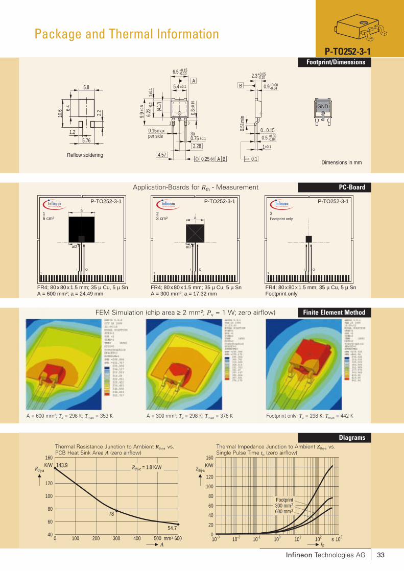
Infineon Technologies AG 33
P-TO252-3-1
1I Q
1
P-TO252-3-1
I Q
P-TO252-3-1
1I Q
1 2 3Footprint only6 cm² 3 cm²
a
a/2
a
a/2
FR4; 80 x 80 x 1.5 mm; 35 µ Cu, 5 µ SnA = 600 mm²; a = 24.49 mm
FR4; 80 x 80 x 1.5 mm; 35 µ Cu, 5 µ SnA = 300 mm²; a = 17.32 mm
FR4; 80 x 80 x 1.5 mm; 35 µ Cu, 5 µ SnFootprint only
5.4 ±0.1
1 3
-0.106.5 +0.15
A
±0.5
9.9 6.22
-0.2
1±0.
1
±0.1
50.
8
0.15±0.1
maxper side 0.75
2.28
4.57
+0.08-0.040.9
2.3 -0.10+0.05
B
min
0.51
±0.11
+0.08-0.040.5
0...0.15
BA0.25 M 0.1
3x
(4.17
)Reflow soldering
5.8
6.4
2.2
10.6
5.76
1.2
GND
Dimensions in mm
Rthj-c = 1.8 K/W
40
Rthj-a Zthj-a
600 mm2300 mm2
160K/W
120
100
80
60
40
20
0
60
80
100
120
K/W160
Footprint
143.9
78
54.7
0A
100 200 300 400 500 600mm2
tp10-3 10-2 10-1 100 101 102 103s
Package and Thermal Information
Infineon Technologies AG 33
Footprint/DimensionsP-TO252-3-1
PC-Board
Finite Element Method
Diagrams
A = 600 mm²; Ta = 298 K; Tmax = 353 K
FEM Simulation (chip area ≥ 2 mm²; Pv = 1 W; zero airflow)
Application-Boards for Rth - Measurement
Thermal Resistance Junction to Ambient Rthj-a vs. PCB Heat Sink Area A (zero airflow)
Thermal Impedance Junction to Ambient Zthj-a vs. Single Pulse Time tp (zero airflow)
Footprint only; Ta = 298 K; Tmax = 442 KA = 300 mm²; Ta = 298 K; Tmax = 376 K

Infineon Technologies AG34
P-TO263-5-1
1 1 1
1 2 3Footprint only6 cm² 3 cm²
P-TO263-5-1 P-TO263-5-1a/2
a
a/2
a
FR4; 80 x 80 x 1.5 mm; 35 µ Cu, 5 µ SnA = 600 mm²; a = 24.49 mm
FR4; 80 x 80 x 1.5 mm; 35 µ Cu, 5 µ SnA = 300 mm²; a = 17.32 mm
FR4; 80 x 80 x 1.5 mm; 35 µ Cu, 5 µ SnFootprint only
Reflow soldering
A
8˚max.BA0.25 M 0.1
±0.210
8.51)
81)
(15)
±0.2
9.25
±0.3
1
5x0.8±0.1
1 5
±0.11.27B
0.5 ±0.1
±0.3
2.7
4.7±
0.5
0.05GND
4x1.7
±0.14.4
±0.10.1
2.4 ±0.1
B
7.91.10.6
10.8
9.4
16.15
4.6
Dimensions in mm
Rthj-c = 1.3 K/WRthj-a
0
Zthj-a
600 mm2300 mm2Footprint
K/W
4045505560657075
85 90K/W
20
10
70
40
30
60
50
35
78.4
52.4
39
0A
100 200 300 400 500 600mm2
tp10-3 10-2 10-1 100 101 102 103s
Infineon Technologies AG34
Footprint/Dimensions
PC-Board
Finite Element Method
Diagrams
P-TO263-5-1
A = 600 mm²; Ta = 298 K; Tmax = 417 K
FEM Simulation (chip area ≥ 2 mm²; Pv = 3 W; zero airflow)
Application-Boards for Rth - Measurement
Thermal Resistance Junction to Ambient Rthj-a vs. PCB Heat Sink Area A (zero airflow)
Thermal Impedance Junction to Ambient Zthj-a vs. Single Pulse Time tp (zero airflow)
A = 300 mm²; Ta = 298 K; Tmax = 455 K Footprint only; Ta = 298 K; Tmax = 533 K

Infineon Technologies AG’s sales offices worldwide –partly represented by Siemens AG
OA
Siemens AG ÖsterreichErdberger Lände 26A-1031 WienT (+43) 1-17 07-3 56 11Fax (+43) 1-17 07-5 59 73
OAUS
Siemens Ltd.885 Mountain HighwayBayswater, Victoria 3153T (+61) 3-97 21 21 11Fax (+61) 3-97 21 72 75
OB
Siemens Electronic ComponentsBeneluxCharleroisesteenweg 116/Chaussée de Charleroi 116B-1060 Brussel/BruxellesT (+32) 2-5 36 69 05Fax (+32) 2-5 36 28 57Email: [email protected]
OBR
Siemens Ltda.SemiconductoresAvenida Mutinga, 3800-Pirituba05110-901 São Paulo-SPT (+55) 11-39 08 25 64Fax (+55) 11-39 08 27 28
OCDN
Infineon Technologies Corporation320 March Road, Suite 604Canada, Ontario K2K 2E2T (+1) 6 13-5 91 63 86Fax (+1) 6 13-5 91 63 89
OCH
Siemens Schweiz AGBauelementeFreilagerstrasse 40CH-8047 ZürichT (+41) 1-4 95 30 65Fax (+41) 1-4 95 50 50
OD
Infineon Technologies AGVölklinger Str. 2D-40219 DüsseldorfT (+49) 2 11-3 99 29 30Fax (+49) 2 11-3 99 14 81
Infineon Technologies AGWerner-von-Siemens-Platz 1D-30880 Laatzen (Hannover)T (+49) 5 11-8 77 22 22Fax (+49) 5 11-8 77 15 20
Infineon Technologies AGVon-der-Tann-Straße 30D-90439 NürnbergT (+49) 9 11-6 54 76 99Fax (+49) 9 11-6 54 76 24
Infineon Technologies AGWeissacher Straße 11D-70499 StuttgartT (+49) 7 11-137 33 14Fax (+49) 7 11-137 24 48
OD
Infineon Technologies AGHalbleiter DistributionRichard-Strauss-Straße 76D-81679 MünchenT (+49) 89-92 21 40 86Fax (+49) 89-92 21 20 71
ODK
Siemens A/SBorupvang 3DK-2750 BallerupT (+45) 44 77-44 77Fax (+45) 44 77-40 17
OE
Siemens S.A.Dpto. ComponentesRonda de Europa, 5E-28760 Tres Cantos-MadridT (+34) 91-5 14 71 51Fax (+34) 91-5 14 70 13
OF
Infineon Technologies France,39/47, Bd. OrnanoF-93527 Saint-Denis CEDEX 2T (+33) 1-49 22 31 00Fax (+33) 1-49 22 28 01
OFIN
Siemens ComponentsScandinaviaP.O.Box 60FIN-02601 Espoo (Helsinki)T (+3 58) 10-5 11 51 51Fax (+3 58) 10-5 11 24 95Email: [email protected]
OGB
Infineon TechnologiesSiemens HouseOldburyGB-Bracknell, BerkshireRG 12 8FZT (+44) 13 44-39 66 18Fax (+44) 13 44-39 66 32
OH
Simacomp Kft.Lajos u. 103H-1036 BudapestT (+36) 1-4 57 16 90Fax (+36) 1-4 57 16 92
OHK
Infineon TechnologiesHong Kong Ltd.Suite 302, Level 3, Festival Walk,80 Tat Chee Avenue,Yam Yat Tsuen,Kowloon TongHong KongT (+8 52) 28 32 05 00Fax (+8 52) 28 27 97 62
OI
Siemens S.p.A.Semiconductor SalesVia Piero e Alberto Pirelli, 10I-20126 MilanoT (+39) 02-66 76 -1Fax (+39) 02-66 76 43 95
OIND
Siemens Ltd.Components DivisionNo. 84 Keonics Electronic CityHosur RoadBangalore 561 229T (+91) 80-8 52 11 22Fax (+91) 80-8 52 11 80
Siemens Ltd.CMP Div, 5th Floor4A Ring Road, IP EstateNew Delhi 110 002T (+91) 11-3 31 99 12Fax (+91) 11-3 31 96 04
Siemens Ltd.CMP Div, 4th Floor130, Pandurang Budhkar Marg,WorliMumbai 400 018T (+91) 22-4 96 21 99Fax (+91) 22-4 96 22 01
OIRL
Siemens Ltd.Electronic Components Division8, Raglan RoadIRL-Dublin 4T (+3 53) 1-2 16 23 42Fax (+3 53) 1-2 16 23 49
OIL
Nisko Ltd.2A,Habarzel St.P.O. Box 5815161580 Tel Aviv – IsrealT (+9 72) 3-7 65 73 00Fax (+9 72) 3-7 65 73 33
OJ
Siemens Components K.K.Talanawa Park Tower 12F & 17F3-20-14, Higashi-Gotanda,Shinagawa-kuTokyo T (+81) 3-54 49 64 11Fax (+81) 3-54 49 64 01
OMAL
Infineon Technologies AGSdn BhdBayan Lepas Free Industrial Zone 111900 PenangT (+60) 4-6 44 99 75Fax (+60) 4-6 41 48 72
ON
Siemens ComponentsScandinaviaØstre Aker vei 24Postboks 10, VeitvetN-0518 OsloT (+47) 22-63 30 00Fax (+47) 22-68 49 13Email: [email protected]
ONL
Siemens Electronic ComponentsBeneluxPostbus 16068NL-2500 BB Den HaagT (+31) 70-3 33 20 65Fax (+31) 70-3 33 28 15Email: [email protected]
ONZ
Siemens Auckland300 Great South RoadGreenlandAucklandT (+64) 9-5 20 30 33Fax (+64) 9-5 20 15 56
OP
Siemens S.A.an Componentes ElectronicosR. Irmaos Siemens, 1AlfragideP-2720-093 AmadoraT (+351) 1-4 17 85 90Fax (+351) 1-4 17 80 83
OPK
Siemens Pakistan EngineeringCo.Ltd.PO Box 1129, Islamabad 4400023 West Jinnah AveIslamabadT (+92) 51-21 22 00Fax (+92) 51-21 16 10
OPL
Siemens SP. z.o.o.ul. Zupnicza 11PL-03-821 WarszawaT (+48) 22-8 70 91 50Fax (+48) 22-8 70 91 59
OROK
Siemens Ltd.Asia Tower, 10th Floor726 Yeoksam-dong, Kang-nam KuCPO Box 3001Seoul 135-080T (+82) 2-5 27 77 00Fax (+82) 2-5 27 77 79
ORUS
INTECH electronicsul. Smolnaya, 24/1203RUS-125 445 MoskvaT (+7) 0 95-4 51 97 37Fax (+7) 0 95-4 51 86 08
OS
Siemens Components ScandinaviaÖsterögatan 1, Box 46S-16493 KistaT (+46) 8-7 03 35 00Fax (+46) 8-7 03 35 01Email:[email protected]
ORC
Infineon TechnologiesAsia Pacific Pte. Ltd.Taiwan Branch10F, No. 136 Nan King East RoadSection 23, TaipeiT (+8 86) 2-27 73 66 06Fax (+8 86) 2-27 71 20 76
OSGP
Infineon Technologies AsiaPacific, Pte. Ltd.168 Kallang WaySingapore 349 253T (+65) 8 40 06 10Fax (+65) 7 42 62 39
OUSA
Infineon TechnologiesCorporation1730 North First StreetSan Jose, CA 95112T (+1) 4 08-5 01 60 00Fax (+1) 4 08-5 01 24 24
Siemens Components, Inc.Optoelectronics Division19000 Homestead RoadCupertino, CA 95014T (+1) 4 08-2 57 79 10Fax (+1) 4 08-7 25 34 39
Siemens Components, Inc.Special Products Division186 Wood Avenue SouthIselin, NJ 08830-2770T (+1) 7 32-9 06 43 00Fax (+1) 7 32-6 32 28 30
OVRC
Infineon TechnologiesHong Kong Ltd.Beijing OfficeRoom 2106, Building AVantone New World PlazaNo. 2 Fu Cheng Men Wai Da Jie100037 BeijingT (+86) 10-68 57 90 -06, -07Fax (+86) 10-68 57 90 08
Infineon TechnologiesHong Kong Ltd.Chengdu OfficeRoom 14J1, Jinyang Mansion58 Tidu StreetChengdu,Sichuan Province 610 016T (+86) 28-6 61 54 46 / 79 51Fax (+86) 28-6 61 01 59
Infineon TechnologiesHong Kong Ltd.Shanghai OfficeRoom 1101, Lucky Target SquareNo. 500 Chengdu Road NorthShanghai 200003T (+86) 21-63 61 26 18/19Fax (+86) 21-63 61 11 67
Infineon TechnologiesHong Kong Ltd.Shenzhen OfficeRoom 1502, Block ATian An International BuildingRenim South RoadShenzhen 518 005T (+86) 7 55-2 28 91 04Fax (+86) 7 55-2 28 02 17
OZA
Siemens Ltd.Components DivisionP.O.B. 3438Halfway House 1685T (+27) 11-6 52 -27 02Fax (+27) 11-6 52 20 42
06.10.99Internet-address: http://www.infineon.com

Qualität hat für uns eineumfassende Bedeutung.Wir wollen allen IhrenAnsprüchen in derbestmöglichen Weisegerecht werden. Es gehtuns also nicht nur um dieProduktqualität – unsereAnstrengungen gelten gleichermaßen derLieferqualität und Logistik,dem Service und Supportsowie allen sonstigen Beratungs- und Betreuungs-leistungen.
Dazu gehört eine bestimmte Geisteshaltung unserer Mitarbeiter. Total Qualityim Denken und Handelngegenüber Kollegen,Lieferanten und Ihnen,unserem Kunden. UnsereLeitlinie ist, jede Aufgabemit „Null Fehlern“ zu lösen – in offenerSichtweise auch über deneigenen Arbeitsplatzhinaus – und uns ständigzu verbessern.Unternehmensweitorientieren wir uns dabeiauch an „top“ (TimeOptimized Processes), umIhnen durch größereSchnelligkeit den entscheidenden Wettbewerbsvorsprung zu verschaffen.Geben Sie uns die Chance, hohe Leistung durchumfassende Qualität zubeweisen.
Wir werden Sie überzeugen.
Quality takes on an all-encompassing significanceat Semiconductor Group.For us it means living upto each and every one ofyour demands in the bestpossible way. So we arenot only concerned withproduct quality. We directour efforts equally atquality of supply andlogistics, service andsupport, as well as all theother ways in which we advise and attend to you.Part of this is the veryspecial attitude of ourstaff. Total Quality inthought and deed,towards co-workers, suppliers and you, ourcustomer. Our guideline is“do everything with zerodefects”, in an openmanner that isdemonstrated beyond your immediate workplace, and to constantly improve.Throughout the corporation we also thinkin terms ofTime Optimized Processes(top), greater speed on our part to give you thatdecisive competitive edge.Give us the chance toprove the best ofperformance through thebest of quality – you willbe convinced.
T o t a l Q u a l i t y M a n a g e m e n t
Published by Infineon Technologies AG
Ordering No. B112-H7482-G1-X-7600Printed in GermanyTB 01005. NB