Embed Size (px)
Citation preview
The Roles of FPGA’s in ReprogrammableSystems
SCOTT HAUCK, MEMBER, IEEE
Reprogrammable systems based on field programmable gatearrays are revolutionizing some forms of computation anddigital logic. As a logic emulation system, they provide ordersof magnitude faster computation than software simulation. As acustom-computing machine, they achieve the highest performanceimplementation for many types of applications. As a multimodesystem, they yield significant hardware savings and provide trulygeneric hardware.
In this paper, we discuss the promise and problems ofreprogrammable systems. This includes an overview of the chipand system architectures of reprogrammable systems as well asthe applications of these systems. We also discuss the challengesand opportunities of future reprogrammable systems.
Keywords—Adaptive computing, custom computing, FPGA,logic emulation, multi-FPGA systems, reconfigurable computing.
I. INTRODUCTION
In the mid-1980’s, a new technology for implementingdigital logic was introduced: the field programmable gatearray (FPGA). These devices could be viewed as eithersmall, slow gate arrays (MPGA’s) or large, expensiveprogrammable logic devices (PLD’s). FPGA’s were capableof implementing significantly more logic than PLD’s, espe-cially because they could implement multilevel logic, whilemost PLD’s were optimized for two-level logic. Althoughthey did not have the capacity of MPGA’s, they also didnot have to be custom fabricated, greatly lowering the costsfor low-volume parts and avoiding long fabrication delays.While many of the FPGA’s were configured by staticrandom access memory (SRAM) cells in the array, this wasgenerally viewed as a liability by potential customers whoworried over the chip’s volatility. Antifuse-based FPGA’salso were developed and for many applications were muchmore attractive, both because they tended to be smaller andfaster due to less programming overhead and because therewas no volatility to the configuration.
Manuscript received May 5, 1997; revised January 20, 1998. This workwas supported in part by the Defense Advanced Research Project Agencyunder Contract DABT63-97-C-0035 and in part by the National ScienceFoundation under Grants CDA-9703228 and MIP-9616572.
The author is with the Department of Electrical and Computer Engi-neering, Northwestern University, Evanston, IL 60208-3118 USA.
Publisher Item Identifier S 0018-9219(98)02669-3.
In the late 1980’s and early 1990’s, there was a growingrealization that the volatility of SRAM-based FPGA’s wasnot a liability but was in fact the key to many new typesof applications. Since the programming of such an FPGAcould be changed by a completely electrical process, muchas a standard processor can be configured to run manyprograms, SRAM-based FPGA’s have become the work-horse of many new reprogrammable applications. Someuses of reprogrammability are simple extensions of thestandard logic implementation tasks for which the FPGA’swere originally designed. An FPGA plus several differentconfigurations stored in read-only memory (ROM) couldbe used for multimode hardware, with the functions onthe chip changed in reaction to the current demands. Also,boards constructed purely from FPGA’s, microcontrollers,and other reprogrammable parts could be truly generichardware, allowing a single board to be reprogrammed toserve many different applications.
Some of the most exciting new uses of FPGA’s movebeyond the implementation of digital logic and insteadharness large numbers of FPGA’s as a general-purposecomputation medium. The circuit mapped onto the FPGA’sneed not be standard hardware equations but can evenbe operations from algorithms and general computations.While these FPGA-based custom-computing machines maynot challenge the performance of microprocessors for allapplications, for computations of the right form, an FPGA-based machine can offer extremely high performance, sur-passing any other programmable solution. Although a cus-tom hardware implementation will be able to beat the powerof any generic programmable system, and thus there mustalways be a faster solution than a multi-FPGA system, thefact is that few applications will ever merit the expenseof creating application-specific solutions. An FPGA-basedcomputing machine, which can be reprogrammed like astandard workstation, offers the highest realizable perfor-mance for many different applications. In a sense, it isa hardware supercomputer, surpassing traditional machinearchitectures for certain applications. This potential hasbeen realized by many different research machines. TheSplash system [50] has provided performance on geneticstring matching that is almost 200 times greater than all
0018–9219/98$10.00 1998 IEEE
PROCEEDINGS OF THE IEEE, VOL. 86, NO. 4, APRIL 1998 615
(a) (b)
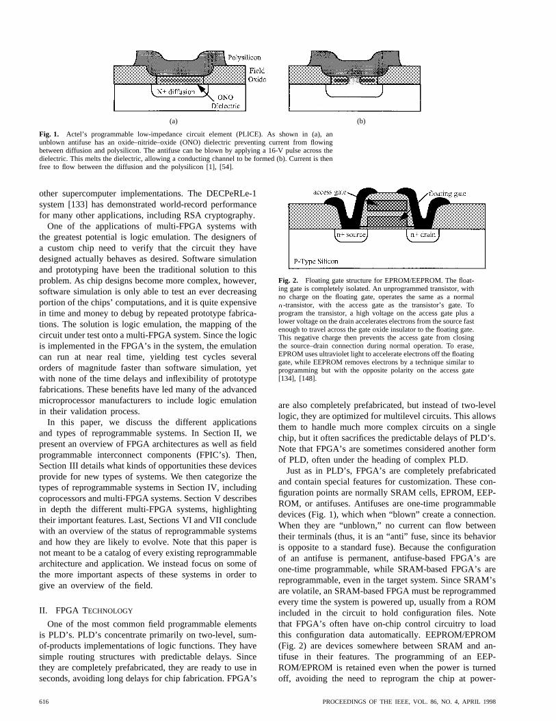
Fig. 1. Actel’s programmable low-impedance circuit element (PLICE). As shown in (a), anunblown antifuse has an oxide–nitride–oxide (ONO) dielectric preventing current from flowingbetween diffusion and polysilicon. The antifuse can be blown by applying a 16-V pulse across thedielectric. This melts the dielectric, allowing a conducting channel to be formed (b). Current is thenfree to flow between the diffusion and the polysilicon [1], [54].
other supercomputer implementations. The DECPeRLe-1system [133] has demonstrated world-record performancefor many other applications, including RSA cryptography.
One of the applications of multi-FPGA systems withthe greatest potential is logic emulation. The designers ofa custom chip need to verify that the circuit they havedesigned actually behaves as desired. Software simulationand prototyping have been the traditional solution to thisproblem. As chip designs become more complex, however,software simulation is only able to test an ever decreasingportion of the chips’ computations, and it is quite expensivein time and money to debug by repeated prototype fabrica-tions. The solution is logic emulation, the mapping of thecircuit under test onto a multi-FPGA system. Since the logicis implemented in the FPGA’s in the system, the emulationcan run at near real time, yielding test cycles severalorders of magnitude faster than software simulation, yetwith none of the time delays and inflexibility of prototypefabrications. These benefits have led many of the advancedmicroprocessor manufacturers to include logic emulationin their validation process.
In this paper, we discuss the different applicationsand types of reprogrammable systems. In Section II, wepresent an overview of FPGA architectures as well as fieldprogrammable interconnect components (FPIC’s). Then,Section III details what kinds of opportunities these devicesprovide for new types of systems. We then categorize thetypes of reprogrammable systems in Section IV, includingcoprocessors and multi-FPGA systems. Section V describesin depth the different multi-FPGA systems, highlightingtheir important features. Last, Sections VI and VII concludewith an overview of the status of reprogrammable systemsand how they are likely to evolve. Note that this paper isnot meant to be a catalog of every existing reprogrammablearchitecture and application. We instead focus on some ofthe more important aspects of these systems in order togive an overview of the field.
II. FPGA TECHNOLOGY
One of the most common field programmable elementsis PLD’s. PLD’s concentrate primarily on two-level, sum-of-products implementations of logic functions. They havesimple routing structures with predictable delays. Sincethey are completely prefabricated, they are ready to use inseconds, avoiding long delays for chip fabrication. FPGA’s
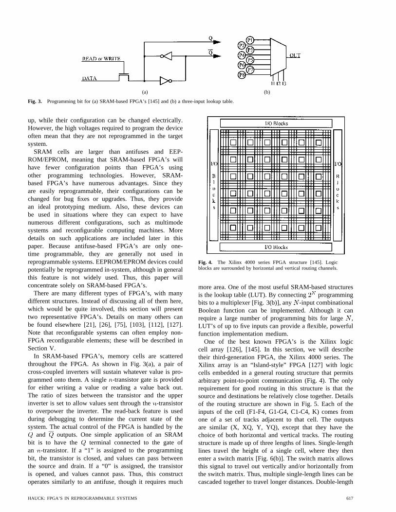
Fig. 2. Floating gate structure for EPROM/EEPROM. The float-ing gate is completely isolated. An unprogrammed transistor, withno charge on the floating gate, operates the same as a normaln-transistor, with the access gate as the transistor’s gate. Toprogram the transistor, a high voltage on the access gate plus alower voltage on the drain accelerates electrons from the source fastenough to travel across the gate oxide insulator to the floating gate.This negative charge then prevents the access gate from closingthe source–drain connection during normal operation. To erase,EPROM uses ultraviolet light to accelerate electrons off the floatinggate, while EEPROM removes electrons by a technique similar toprogramming but with the opposite polarity on the access gate[134], [148].
are also completely prefabricated, but instead of two-levellogic, they are optimized for multilevel circuits. This allowsthem to handle much more complex circuits on a singlechip, but it often sacrifices the predictable delays of PLD’s.Note that FPGA’s are sometimes considered another formof PLD, often under the heading of complex PLD.
Just as in PLD’s, FPGA’s are completely prefabricatedand contain special features for customization. These con-figuration points are normally SRAM cells, EPROM, EEP-ROM, or antifuses. Antifuses are one-time programmabledevices (Fig. 1), which when “blown” create a connection.When they are “unblown,” no current can flow betweentheir terminals (thus, it is an “anti” fuse, since its behavioris opposite to a standard fuse). Because the configurationof an antifuse is permanent, antifuse-based FPGA’s areone-time programmable, while SRAM-based FPGA’s arereprogrammable, even in the target system. Since SRAM’sare volatile, an SRAM-based FPGA must be reprogrammedevery time the system is powered up, usually from a ROMincluded in the circuit to hold configuration files. Notethat FPGA’s often have on-chip control circuitry to loadthis configuration data automatically. EEPROM/EPROM(Fig. 2) are devices somewhere between SRAM and an-tifuse in their features. The programming of an EEP-ROM/EPROM is retained even when the power is turnedoff, avoiding the need to reprogram the chip at power-
616 PROCEEDINGS OF THE IEEE, VOL. 86, NO. 4, APRIL 1998
(a) (b)
Fig. 3. Programming bit for (a) SRAM-based FPGA’s [145] and (b) a three-input lookup table.
up, while their configuration can be changed electrically.However, the high voltages required to program the deviceoften mean that they are not reprogrammed in the targetsystem.
SRAM cells are larger than antifuses and EEP-ROM/EPROM, meaning that SRAM-based FPGA’s willhave fewer configuration points than FPGA’s usingother programming technologies. However, SRAM-based FPGA’s have numerous advantages. Since theyare easily reprogrammable, their configurations can bechanged for bug fixes or upgrades. Thus, they providean ideal prototyping medium. Also, these devices canbe used in situations where they can expect to havenumerous different configurations, such as multimodesystems and reconfigurable computing machines. Moredetails on such applications are included later in thispaper. Because antifuse-based FPGA’s are only one-time programmable, they are generally not used inreprogrammable systems. EEPROM/EPROM devices couldpotentially be reprogrammed in-system, although in generalthis feature is not widely used. Thus, this paper willconcentrate solely on SRAM-based FPGA’s.
There are many different types of FPGA’s, with manydifferent structures. Instead of discussing all of them here,which would be quite involved, this section will presenttwo representative FPGA’s. Details on many others canbe found elsewhere [21], [26], [75], [103], [112], [127].Note that reconfigurable systems can often employ non-FPGA reconfigurable elements; these will be described inSection V.
In SRAM-based FPGA’s, memory cells are scatteredthroughout the FPGA. As shown in Fig. 3(a), a pair ofcross-coupled inverters will sustain whatever value is pro-grammed onto them. A single-transistor gate is providedfor either writing a value or reading a value back out.The ratio of sizes between the transistor and the upperinverter is set to allow values sent through the-transistorto overpower the inverter. The read-back feature is usedduring debugging to determine the current state of thesystem. The actual control of the FPGA is handled by the
and outputs. One simple application of an SRAMbit is to have the terminal connected to the gate ofan -transistor. If a “1” is assigned to the programmingbit, the transistor is closed, and values can pass betweenthe source and drain. If a “0” is assigned, the transistoris opened, and values cannot pass. Thus, this constructoperates similarly to an antifuse, though it requires much
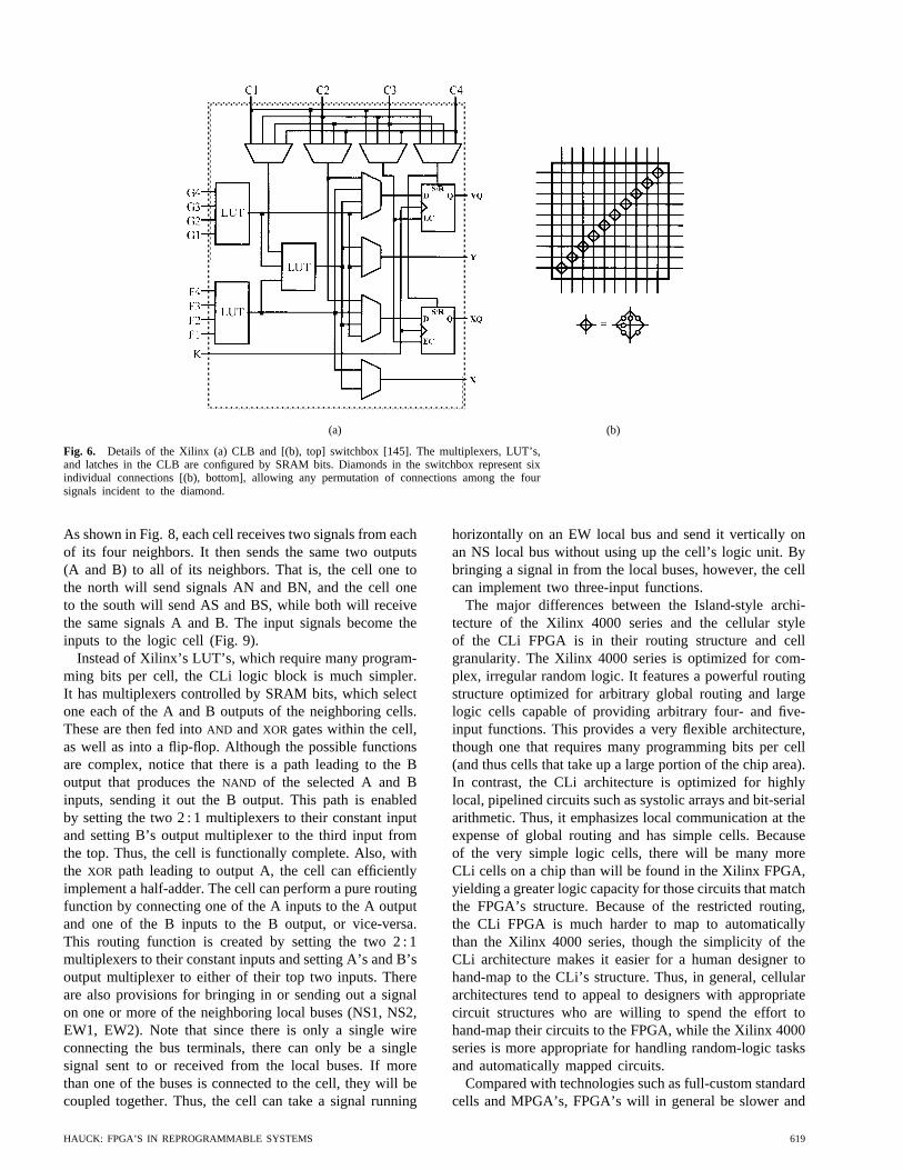
Fig. 4. The Xilinx 4000 series FPGA structure [145]. Logicblocks are surrounded by horizontal and vertical routing channels.
more area. One of the most useful SRAM-based structuresis the lookup table (LUT). By connecting programmingbits to a multiplexer [Fig. 3(b)], any -input combinationalBoolean function can be implemented. Although it canrequire a large number of programming bits for large,LUT’s of up to five inputs can provide a flexible, powerfulfunction implementation medium.
One of the best known FPGA’s is the Xilinx logiccell array [126], [145]. In this section, we will describetheir third-generation FPGA, the Xilinx 4000 series. TheXilinx array is an “Island-style” FPGA [127] with logiccells embedded in a general routing structure that permitsarbitrary point-to-point communication (Fig. 4). The onlyrequirement for good routing in this structure is that thesource and destinations be relatively close together. Detailsof the routing structure are shown in Fig. 5. Each of theinputs of the cell (F1-F4, G1-G4, C1-C4, K) comes fromone of a set of tracks adjacent to that cell. The outputsare similar (X, XQ, Y, YQ), except that they have thechoice of both horizontal and vertical tracks. The routingstructure is made up of three lengths of lines. Single-lengthlines travel the height of a single cell, where they thenenter a switch matrix [Fig. 6(b)]. The switch matrix allowsthis signal to travel out vertically and/or horizontally fromthe switch matrix. Thus, multiple single-length lines can becascaded together to travel longer distances. Double-length
HAUCK: FPGA’S IN REPROGRAMMABLE SYSTEMS 617
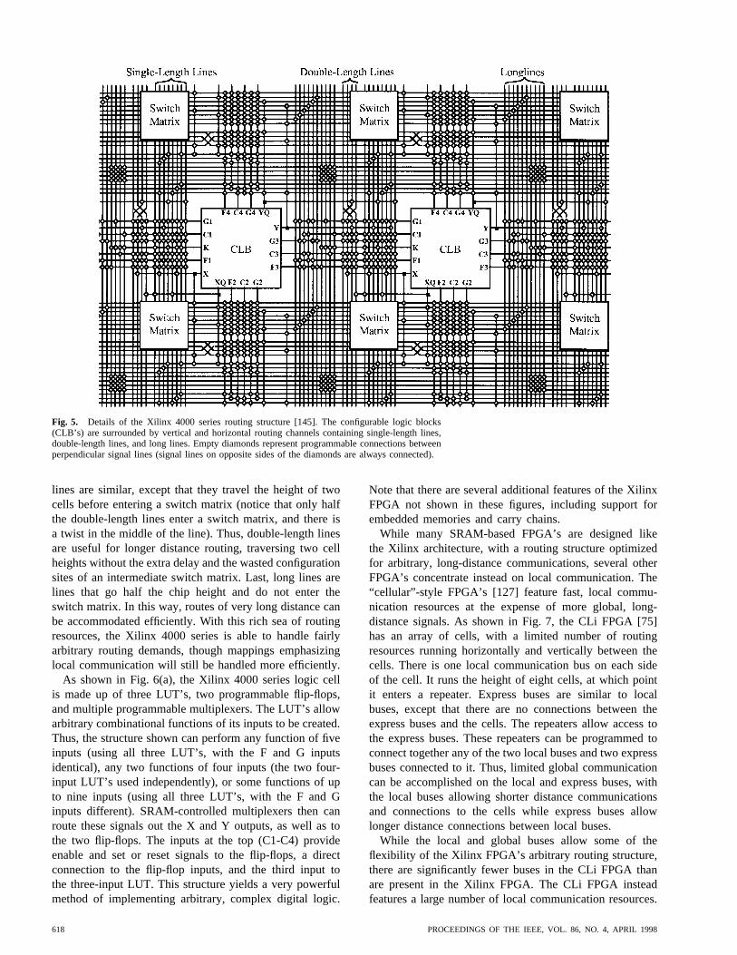
Fig. 5. Details of the Xilinx 4000 series routing structure [145]. The configurable logic blocks(CLB’s) are surrounded by vertical and horizontal routing channels containing single-length lines,double-length lines, and long lines. Empty diamonds represent programmable connections betweenperpendicular signal lines (signal lines on opposite sides of the diamonds are always connected).
lines are similar, except that they travel the height of twocells before entering a switch matrix (notice that only halfthe double-length lines enter a switch matrix, and there isa twist in the middle of the line). Thus, double-length linesare useful for longer distance routing, traversing two cellheights without the extra delay and the wasted configurationsites of an intermediate switch matrix. Last, long lines arelines that go half the chip height and do not enter theswitch matrix. In this way, routes of very long distance canbe accommodated efficiently. With this rich sea of routingresources, the Xilinx 4000 series is able to handle fairlyarbitrary routing demands, though mappings emphasizinglocal communication will still be handled more efficiently.
As shown in Fig. 6(a), the Xilinx 4000 series logic cellis made up of three LUT’s, two programmable flip-flops,and multiple programmable multiplexers. The LUT’s allowarbitrary combinational functions of its inputs to be created.Thus, the structure shown can perform any function of fiveinputs (using all three LUT’s, with the F and G inputsidentical), any two functions of four inputs (the two four-input LUT’s used independently), or some functions of upto nine inputs (using all three LUT’s, with the F and Ginputs different). SRAM-controlled multiplexers then canroute these signals out the X and Y outputs, as well as tothe two flip-flops. The inputs at the top (C1-C4) provideenable and set or reset signals to the flip-flops, a directconnection to the flip-flop inputs, and the third input tothe three-input LUT. This structure yields a very powerfulmethod of implementing arbitrary, complex digital logic.
Note that there are several additional features of the XilinxFPGA not shown in these figures, including support forembedded memories and carry chains.
While many SRAM-based FPGA’s are designed likethe Xilinx architecture, with a routing structure optimizedfor arbitrary, long-distance communications, several otherFPGA’s concentrate instead on local communication. The“cellular”-style FPGA’s [127] feature fast, local commu-nication resources at the expense of more global, long-distance signals. As shown in Fig. 7, the CLi FPGA [75]has an array of cells, with a limited number of routingresources running horizontally and vertically between thecells. There is one local communication bus on each sideof the cell. It runs the height of eight cells, at which pointit enters a repeater. Express buses are similar to localbuses, except that there are no connections between theexpress buses and the cells. The repeaters allow access tothe express buses. These repeaters can be programmed toconnect together any of the two local buses and two expressbuses connected to it. Thus, limited global communicationcan be accomplished on the local and express buses, withthe local buses allowing shorter distance communicationsand connections to the cells while express buses allowlonger distance connections between local buses.
While the local and global buses allow some of theflexibility of the Xilinx FPGA’s arbitrary routing structure,there are significantly fewer buses in the CLi FPGA thanare present in the Xilinx FPGA. The CLi FPGA insteadfeatures a large number of local communication resources.
618 PROCEEDINGS OF THE IEEE, VOL. 86, NO. 4, APRIL 1998
(a) (b)
Fig. 6. Details of the Xilinx (a) CLB and [(b), top] switchbox [145]. The multiplexers, LUT’s,and latches in the CLB are configured by SRAM bits. Diamonds in the switchbox represent sixindividual connections [(b), bottom], allowing any permutation of connections among the foursignals incident to the diamond.
As shown in Fig. 8, each cell receives two signals from eachof its four neighbors. It then sends the same two outputs(A and B) to all of its neighbors. That is, the cell one tothe north will send signals AN and BN, and the cell oneto the south will send AS and BS, while both will receivethe same signals A and B. The input signals become theinputs to the logic cell (Fig. 9).
Instead of Xilinx’s LUT’s, which require many program-ming bits per cell, the CLi logic block is much simpler.It has multiplexers controlled by SRAM bits, which selectone each of the A and B outputs of the neighboring cells.These are then fed intoAND andXOR gates within the cell,as well as into a flip-flop. Although the possible functionsare complex, notice that there is a path leading to the Boutput that produces theNAND of the selected A and Binputs, sending it out the B output. This path is enabledby setting the two 2 : 1 multiplexers to their constant inputand setting B’s output multiplexer to the third input fromthe top. Thus, the cell is functionally complete. Also, withthe XOR path leading to output A, the cell can efficientlyimplement a half-adder. The cell can perform a pure routingfunction by connecting one of the A inputs to the A outputand one of the B inputs to the B output, or vice-versa.This routing function is created by setting the two 2 : 1multiplexers to their constant inputs and setting A’s and B’soutput multiplexer to either of their top two inputs. Thereare also provisions for bringing in or sending out a signalon one or more of the neighboring local buses (NS1, NS2,EW1, EW2). Note that since there is only a single wireconnecting the bus terminals, there can only be a singlesignal sent to or received from the local buses. If morethan one of the buses is connected to the cell, they will becoupled together. Thus, the cell can take a signal running
horizontally on an EW local bus and send it vertically onan NS local bus without using up the cell’s logic unit. Bybringing a signal in from the local buses, however, the cellcan implement two three-input functions.
The major differences between the Island-style archi-tecture of the Xilinx 4000 series and the cellular styleof the CLi FPGA is in their routing structure and cellgranularity. The Xilinx 4000 series is optimized for com-plex, irregular random logic. It features a powerful routingstructure optimized for arbitrary global routing and largelogic cells capable of providing arbitrary four- and five-input functions. This provides a very flexible architecture,though one that requires many programming bits per cell(and thus cells that take up a large portion of the chip area).In contrast, the CLi architecture is optimized for highlylocal, pipelined circuits such as systolic arrays and bit-serialarithmetic. Thus, it emphasizes local communication at theexpense of global routing and has simple cells. Becauseof the very simple logic cells, there will be many moreCLi cells on a chip than will be found in the Xilinx FPGA,yielding a greater logic capacity for those circuits that matchthe FPGA’s structure. Because of the restricted routing,the CLi FPGA is much harder to map to automaticallythan the Xilinx 4000 series, though the simplicity of theCLi architecture makes it easier for a human designer tohand-map to the CLi’s structure. Thus, in general, cellulararchitectures tend to appeal to designers with appropriatecircuit structures who are willing to spend the effort tohand-map their circuits to the FPGA, while the Xilinx 4000series is more appropriate for handling random-logic tasksand automatically mapped circuits.
Compared with technologies such as full-custom standardcells and MPGA’s, FPGA’s will in general be slower and
HAUCK: FPGA’S IN REPROGRAMMABLE SYSTEMS 619
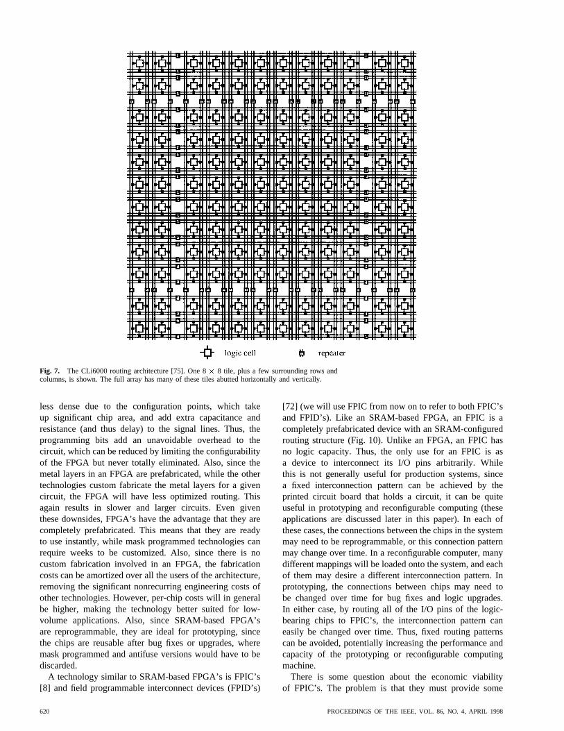
Fig. 7. The CLi6000 routing architecture [75]. One 8� 8 tile, plus a few surrounding rows andcolumns, is shown. The full array has many of these tiles abutted horizontally and vertically.
less dense due to the configuration points, which takeup significant chip area, and add extra capacitance andresistance (and thus delay) to the signal lines. Thus, theprogramming bits add an unavoidable overhead to thecircuit, which can be reduced by limiting the configurabilityof the FPGA but never totally eliminated. Also, since themetal layers in an FPGA are prefabricated, while the othertechnologies custom fabricate the metal layers for a givencircuit, the FPGA will have less optimized routing. Thisagain results in slower and larger circuits. Even giventhese downsides, FPGA’s have the advantage that they arecompletely prefabricated. This means that they are readyto use instantly, while mask programmed technologies canrequire weeks to be customized. Also, since there is nocustom fabrication involved in an FPGA, the fabricationcosts can be amortized over all the users of the architecture,removing the significant nonrecurring engineering costs ofother technologies. However, per-chip costs will in generalbe higher, making the technology better suited for low-volume applications. Also, since SRAM-based FPGA’sare reprogrammable, they are ideal for prototyping, sincethe chips are reusable after bug fixes or upgrades, wheremask programmed and antifuse versions would have to bediscarded.
A technology similar to SRAM-based FPGA’s is FPIC’s[8] and field programmable interconnect devices (FPID’s)
[72] (we will use FPIC from now on to refer to both FPIC’sand FPID’s). Like an SRAM-based FPGA, an FPIC is acompletely prefabricated device with an SRAM-configuredrouting structure (Fig. 10). Unlike an FPGA, an FPIC hasno logic capacity. Thus, the only use for an FPIC is asa device to interconnect its I/O pins arbitrarily. Whilethis is not generally useful for production systems, sincea fixed interconnection pattern can be achieved by theprinted circuit board that holds a circuit, it can be quiteuseful in prototyping and reconfigurable computing (theseapplications are discussed later in this paper). In each ofthese cases, the connections between the chips in the systemmay need to be reprogrammable, or this connection patternmay change over time. In a reconfigurable computer, manydifferent mappings will be loaded onto the system, and eachof them may desire a different interconnection pattern. Inprototyping, the connections between chips may need tobe changed over time for bug fixes and logic upgrades.In either case, by routing all of the I/O pins of the logic-bearing chips to FPIC’s, the interconnection pattern caneasily be changed over time. Thus, fixed routing patternscan be avoided, potentially increasing the performance andcapacity of the prototyping or reconfigurable computingmachine.
There is some question about the economic viabilityof FPIC’s. The problem is that they must provide some
620 PROCEEDINGS OF THE IEEE, VOL. 86, NO. 4, APRIL 1998
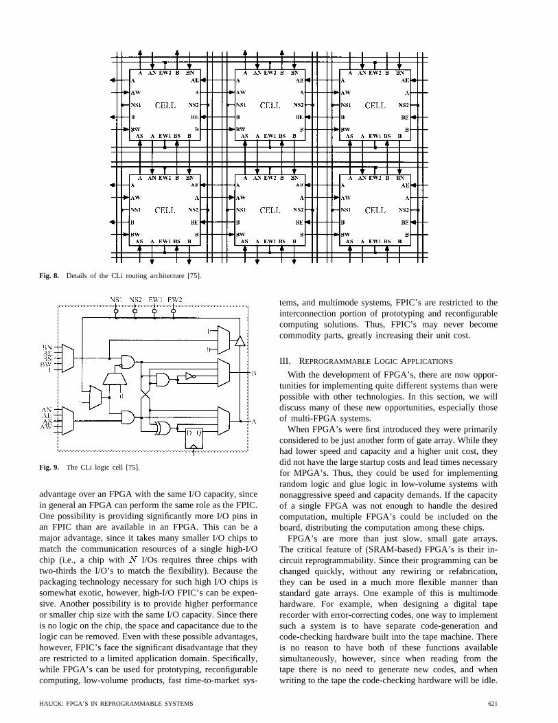
Fig. 8. Details of the CLi routing architecture [75].
Fig. 9. The CLi logic cell [75].
advantage over an FPGA with the same I/O capacity, sincein general an FPGA can perform the same role as the FPIC.One possibility is providing significantly more I/O pins inan FPIC than are available in an FPGA. This can be amajor advantage, since it takes many smaller I/O chips tomatch the communication resources of a single high-I/Ochip (i.e., a chip with I/Os requires three chips withtwo-thirds the I/O’s to match the flexibility). Because thepackaging technology necessary for such high I/O chips issomewhat exotic, however, high-I/O FPIC’s can be expen-sive. Another possibility is to provide higher performanceor smaller chip size with the same I/O capacity. Since thereis no logic on the chip, the space and capacitance due to thelogic can be removed. Even with these possible advantages,however, FPIC’s face the significant disadvantage that theyare restricted to a limited application domain. Specifically,while FPGA’s can be used for prototyping, reconfigurablecomputing, low-volume products, fast time-to-market sys-
tems, and multimode systems, FPIC’s are restricted to theinterconnection portion of prototyping and reconfigurablecomputing solutions. Thus, FPIC’s may never becomecommodity parts, greatly increasing their unit cost.
III. REPROGRAMMABLE LOGIC APPLICATIONS
With the development of FPGA’s, there are now oppor-tunities for implementing quite different systems than werepossible with other technologies. In this section, we willdiscuss many of these new opportunities, especially thoseof multi-FPGA systems.
When FPGA’s were first introduced they were primarilyconsidered to be just another form of gate array. While theyhad lower speed and capacity and a higher unit cost, theydid not have the large startup costs and lead times necessaryfor MPGA’s. Thus, they could be used for implementingrandom logic and glue logic in low-volume systems withnonaggressive speed and capacity demands. If the capacityof a single FPGA was not enough to handle the desiredcomputation, multiple FPGA’s could be included on theboard, distributing the computation among these chips.
FPGA’s are more than just slow, small gate arrays.The critical feature of (SRAM-based) FPGA’s is their in-circuit reprogrammability. Since their programming can bechanged quickly, without any rewiring or refabrication,they can be used in a much more flexible manner thanstandard gate arrays. One example of this is multimodehardware. For example, when designing a digital taperecorder with error-correcting codes, one way to implementsuch a system is to have separate code-generation andcode-checking hardware built into the tape machine. Thereis no reason to have both of these functions availablesimultaneously, however, since when reading from thetape there is no need to generate new codes, and whenwriting to the tape the code-checking hardware will be idle.
HAUCK: FPGA’S IN REPROGRAMMABLE SYSTEMS 621
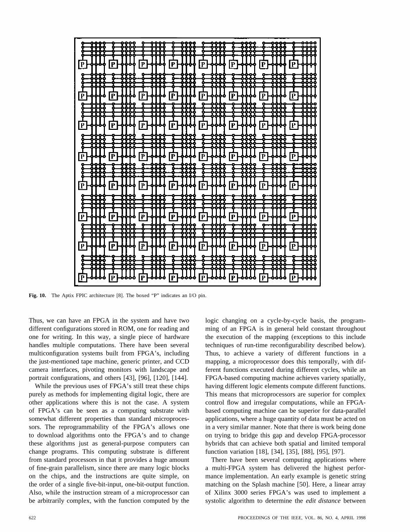
Fig. 10. The Aptix FPIC architecture [8]. The boxed “P” indicates an I/O pin.
Thus, we can have an FPGA in the system and have twodifferent configurations stored in ROM, one for reading andone for writing. In this way, a single piece of hardwarehandles multiple computations. There have been severalmulticonfiguration systems built from FPGA’s, includingthe just-mentioned tape machine, generic printer, and CCDcamera interfaces, pivoting monitors with landscape andportrait configurations, and others [43], [96], [120], [144].
While the previous uses of FPGA’s still treat these chipspurely as methods for implementing digital logic, there areother applications where this is not the case. A systemof FPGA’s can be seen as a computing substrate withsomewhat different properties than standard microproces-sors. The reprogrammability of the FPGA’s allows oneto download algorithms onto the FPGA’s and to changethese algorithms just as general-purpose computers canchange programs. This computing substrate is differentfrom standard processors in that it provides a huge amountof fine-grain parallelism, since there are many logic blockson the chips, and the instructions are quite simple, onthe order of a single five-bit-input, one-bit-output function.Also, while the instruction stream of a microprocessor canbe arbitrarily complex, with the function computed by the
logic changing on a cycle-by-cycle basis, the program-ming of an FPGA is in general held constant throughoutthe execution of the mapping (exceptions to this includetechniques of run-time reconfigurability described below).Thus, to achieve a variety of different functions in amapping, a microprocessor does this temporally, with dif-ferent functions executed during different cycles, while anFPGA-based computing machine achieves variety spatially,having different logic elements compute different functions.This means that microprocessors are superior for complexcontrol flow and irregular computations, while an FPGA-based computing machine can be superior for data-parallelapplications, where a huge quantity of data must be acted onin a very similar manner. Note that there is work being doneon trying to bridge this gap and develop FPGA-processorhybrids that can achieve both spatial and limited temporalfunction variation [18], [34], [35], [88], [95], [97].
There have been several computing applications wherea multi-FPGA system has delivered the highest perfor-mance implementation. An early example is genetic stringmatching on the Splash machine [50]. Here, a linear arrayof Xilinx 3000 series FPGA’s was used to implement asystolic algorithm to determine theedit distancebetween
622 PROCEEDINGS OF THE IEEE, VOL. 86, NO. 4, APRIL 1998
two strings. The edit distance is the minimum number of in-sertions and deletions necessary to transform one string intoanother, so the strings “flea” and “fleet” would have an editdistance of three (delete “a” and insert “et” to go from “flea”to “fleet”). As shown in [89], a dynamic-programmingsolution to this problem can be implemented in the Splashsystem as a linear systolic circuit, with the strings to becompared flowing in opposite directions through the lineararray. Processing can occur throughout the linear arraysimultaneously, with only local communication necessary,producing a huge amount of fine-grain parallelism. This isexactly the type of computation that maps well onto a multi-FPGA system. The Splash implementation was able to offeran extremely high-performance solution for this application,achieving performance approximately 200 times faster thansupercomputer implementations. There have been manyother applications where a multi-FPGA system has offeredthe highest performance solution, including mathematicsapplications such as long multiplication [15], [133], mod-ular multiplication [32], and RSA cryptography [133];physics applications such as real-time pattern recognition inhigh-energy physics [67], Monte Carlo algorithms for sta-tistical physics [30], [99], second-level triggers for particlecolliders [98], and Heat and Laplace equation solvers [133];general algorithms such as the Traveling Salesman Problem[52], Monte Carlo yield modeling [69], genetic optimizationalgorithms [53], [118], region detection and labeling [108],stereo matching for stereo vision [133], hidden Markovmodeling for speech recognition [116], and genetic database searches [66], [85], [89].
One of the most successful uses for FPGA-based com-putation is in application-specific integrated circuit (ASIC)logic emulation. The idea is that the designers of a customASIC need to make sure that the circuit they designedcorrectly implements the desired computation. Softwaresimulation can perform these checks but does so quiteslowly. In logic emulation, the circuit to be tested is insteadmapped onto a multi-FPGA system, yielding a solutionseveral orders of magnitude faster than software simulation.
Logic emulation shares many of the advantages (anddisadvantages) of both prototyping and software simulation.Like a prototype, the circuit to be evaluated is implementedin hardware so that it can achieve high-performance testcycles. Like software simulation, however, the emulationcan easily be observed and altered to help isolate bugs.Logic emulation takes a gate-level description of a logiccircuit and maps it onto a multi-FPGA system. This multi-FPGA system is a prefabricated, reprogrammable computeengine that can be configured to implement the desiredcircuitry in a matter of seconds. However, to transformthe circuit description into a mapping suitable for thismulti-FPGA system can take many hours to complete. Thismapping process is usually completely automated by theemulator’s system software. Once the circuit is mapped tothe multi-FPGA system, the emulator provides a complete,functional implementation of the circuit that can evaluatemillions of circuit cycles per second. This is orders ofmagnitude faster than even simulation accelerators, since
the multi-FPGA system can implement the complete circuitin parallel, while accelerators simply provide one or moresequential logic evaluation processors.
Emulators provide a middle ground between softwaresimulation and prototyping. Compared to software simula-tion, an emulation executes much faster than a simulation.It can take a long time to map a circuit onto the emulator,however, and it is more difficult to observe and modify thebehavior of the circuit. Thus, software simulation is a betterchoice for testing small subcircuits or small numbers ofcomplete circuit cycles, where the software’s flexibility andease of use outweighs the performance penalties. Comparedto a prototype, an emulation is much easier and faster tocreate, and it has much greater observability, controllability,and modifiability than a prototype. However, the emulationcannot run at the same speed as the target system. Thus,the emulator is a much better choice for providing a hugenumber of test cycles than a prototype when one expects tofind bugs in the system, but it is no replacement for finalcheckout of the system via a prototype. For circuits thatwill execute software programs, an emulator can be usedto debug this software much earlier in the design processthan a physical prototype. This is because an emulation canbe created from a high-level specification of the circuit,while prototyping must wait until the complete circuit hasbeen designed. Simulation in general cannot be used forsoftware development, since it is much too slow to executeenough cycles of the software. Also, just like a prototype, anemulation can be given to the end user so that the circuit canbe evaluated before the design is completed. In this way, theuser can get a much better feeling for whether the designwill fulfill the user’s needs, something that is difficult withjust a written specification. The emulation can be insertedinto the target environment (as long as some method for re-ducing the performance demands on the system can be pro-vided [59], [60], [107]), and the system can be evaluated ina more realistic setting. This helps both to debug the circuitand to test the circuit interfaces and environment. For ex-ample, often a custom ASIC and the circuit board that willcontain it will be developed simultaneously. An emulationof the ASIC can be inserted into this circuit-board proto-type, testing both the ASIC functions and the board design.
One limitation of emulation is that it retains only thefunctional behavior of the circuit, which means that vali-dation of the performance and timing features of a circuitcannot be performed on a logic emulator. Once a prototypeis constructed, both logic emulation and software simulationare still valuable tools [48]. When an error is found in aphysical prototype, it can be difficult to isolate the exactcause in the circuit. An emulator can be used to reproducethe failure, since it can execute nearly as many cyclesas the prototype, and the emulator’s observability can beused to isolate the failure. Then, detailed testing can beperformed by software simulation. Thus, logic emulationplays a complementary role to both software simulationand prototyping in logic validation.
An emerging application of FPGA-based computing isthe training and execution of neural networks. A neural
HAUCK: FPGA’S IN REPROGRAMMABLE SYSTEMS 623
network is a powerful computational model based on thestructure of neurons in the brain. These systems haveproven effective for tasks such as pattern recognition andclassification. One important aspect of these nets is thateach of the basic elements in the network must be config-ured for a given problem. This configuration (or “learning”)process revolves around exposing the network to situationswhere the correct answer is known and adjusting thenetwork’s configuration so that it returns the correct answer.The execution of a neural network can be time consum-ing on a standard processor, especially for the repeatedexecution runs required during the training process. Thus,there is great interest in implementing neural networks inreprogrammable systems, both because of the speed benefitsand because the reprogrammability of the FPGA’s cansupport the reconfiguration necessary to program a neuralnetwork.
Systems like the just-mentioned neural-network imple-mentations, as well as multimode systems, take advantageof an FPGA’s reprogrammability by changing the chip’sprogramming over time, much as a standard processorcontext-switches to a new program. However, it is possibleto make more aggressive use of this ability to developnew types of applications. The FPGA can be viewed asa demand-paged hardware resource, yielding “virtual hard-ware” similar to virtual memory in today’s computers. Insuch systems (usually grouped under the termdynamicallyreconfigurableor run-time reconfiguration), an applicationwill require many different types of computations, andeach of these computations has a separate mapping to thereprogrammable logic. For example, an image processingapplication for object thinning may require separate pre-filtering and thresholding steps before running the thinningoperation, each of which could be implemented in a sepa-rate FPGA mapping [140]. Although these mappings couldbe spread across multiple FPGA’s, these steps must takeplace sequentially, and in a multi-FPGA system, only onemapping would be actively computing at a time. Run-time reconfiguration saves hardware by reusing the sameresource. It also relaxes the upper limit on the number ofconfigurations allowed, since in a multi-FPGA system, thenumber of FPGA’s available is usually fixed (either bythe architecture or by the current hardware instantiation),while a run-time reconfigured system can have as manyconfigurations as there is storage space to hold them.Because of these advantages, there has been a lot ofwork on run-time reconfigurable systems, applications, andsupport tools [35], [40], [46], [51], [56], [76], [80], [90],[91], [93], [111], [113], [117], [131], [141]. Note thatthis approach can be taken even further to local run-timereconfiguration [20], [29], [71], [92], [94], [122], [139],[140]. In a locally run-time reconfigurable system, differentphases of an algorithm can have mappings to just a portionof the FPGA. Multiple configurations can be loaded intothe system, with each configuration occupying differentportions of the FPGA. In this way, the FPGA becomesa hardware cache, with the set of loaded mappings varyingover time based on the requirements of the algorithm. When
a configuration is needed that is currently not in the FPGA,it is loaded into the FPGA, replacing other mappings thatare no longer required. In this way, multiple small mappingscan coexist in the FPGA, potentially eliminating most of thetime overhead of complete FPGA reprogramming for eachsmall mapping.
Reprogrammable systems have a great deal of poten-tial for providing higher performance solutions to manydifferent applications. However, just as it is importantto carefully select the type of application mapped to amulti-FPGA system, it is also crucial to carefully constructthe reprogrammable system to support these applications.In Section IV, we discuss the types of reprogrammablesystems.
IV. REPROGRAMMABLE SYSTEMS
There is a wide variety of different roles for repro-grammable logic, and these roles can require very differ-ent types of reprogrammable systems. Some are isolated,small-capacity systems used for the replacement of smalldigital logic systems. Others have hundreds or thousands ofFPGA’s, with capacities into the millions of gates, whichrival supercomputers for certain types of applications.
One of the most common types of reprogrammablesystems is a one-FPGA or two-FPGA system used forinterfacing and other standard logic tasks. With the additionof memory resources and the appropriate interface circuitry,these systems provide a much greater flexibility than tradi-tional implementations. These systems can be prefabricatedand used for multiple applications, reducing both designtime and inventory risk. When a new application must bedeveloped, the designer need only specify the logic requiredto handle the new functions. This logic can then be automat-ically mapped to the FPGA’s, and the prefabricated systemcan be used immediately. This contrasts with traditionalapproaches, which have the extra time and complexity costsof custom board design and fabrication.
Reprogrammable systems need not be prefabricated. Infact, there is a great deal of interest in automatic creation ofcustom application-specific reprogrammable systems [27],[70], [82], [83], [143]. In such an approach, the logic isagain specified by the designer, and automatic tools mapthis circuitry into FPGA logic. Instead of being constrainedto a predefined topology, however, the mapping tools areinstead allowed to develop a custom multichip solution.Because the chips are interconnected in response to theneeds of a specific application, a much more highly opti-mized solution can be developed. This can be a significantsavings, since premade systems often present the designeror the mapping tools with a very constrained system, greatlycomplicating the mapping process. However, there are twodownsides to this approach. First, if a reprogrammablesystem is custom designed in response to a specific ap-plication, then obviously this system cannot be premade.Thus, the user must wait for the new board to be fabricated.Also, there is little chance of reusing this system forother applications. This increases the hardware costs since
624 PROCEEDINGS OF THE IEEE, VOL. 86, NO. 4, APRIL 1998
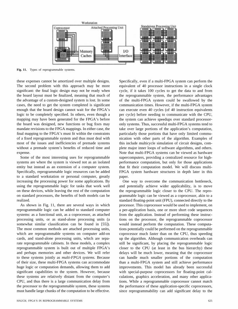
Fig. 11. Types of reprogrammable systems.
these expenses cannot be amortized over multiple designs.The second problem with this approach may be moresignificant: the final logic design may not be ready whenthe board layout must be finalized, meaning that much ofthe advantage of a custom-designed system is lost. In somecases, the need to get the system completed is significantenough that the board design cannot wait for the FPGA’slogic to be completely specified. In others, even though amapping may have been generated for the FPGA’s beforethe board was designed, new functions or bug fixes maymandate revisions to the FPGA mappings. In either case, thefinal mapping to the FPGA’s must fit within the constraintsof a fixed reprogrammable system and thus must deal withmost of the issues and inefficiencies of premade systemswithout a premade system’s benefits of reduced time andexpense.
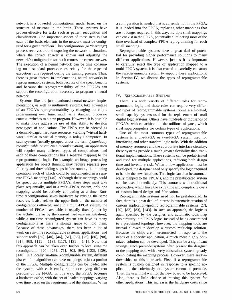
Some of the most interesting uses for reprogrammablesystems are where the system is viewed not as an isolatedentity but instead as an extension of a computer system.Specifically, reprogrammable logic resources can be addedto a standard workstation or personal computer, greatlyincreasing the processing power for some applications. Byusing the reprogrammable logic for tasks that work wellon these devices, while leaving the rest of the computationon standard processors, the benefits of both models can berealized.
As shown in Fig. 11, there are several ways in whichreprogrammable logic can be added to standard computersystems: as a functional unit, as a coprocessor, as attachedprocessing units, or as stand-alone processing units (asomewhat similar classification can be found in [55]).The most common methods are attached processing units,which are reprogrammable systems on computer add-oncards, and stand-alone processing units, which are sepa-rate reprogrammable cabinets. In these models, a complexreprogrammable system is built out of multiple FPGA’sand perhaps memories and other devices. We will referto these systems jointly asmulti-FPGA systems.Becauseof their size, these multi-FPGA systems can accommodatehuge logic or computation demands, allowing them to addsignificant capabilities to the system. However, becausethese systems are relatively distant from the computer’sCPU, and thus there is a large communication delay fromthe processor to the reprogrammable system, these systemsmust handle large chunks of the computation to be effective.
Specifically, even if a multi-FPGA system can perform theequivalent of 40 processor instructions in a single clockcycle, if it takes 100 cycles to get the data to and fromthe reprogrammable system, the performance advantagesof the multi-FPGA system could be swallowed by thecommunication times. However, if the multi-FPGA systemcan execute even 40 cycles (of 40 instruction equivalentsper cycle) before needing to communicate with the CPU,the system can achieve speedups over standard processor-only systems. Thus, successful multi-FPGA systems tend totake over large portions of the application’s computation,particularly those portions that have only limited commu-nication with other parts of the algorithm. Examples ofthis include multicycle simulation of circuit designs, com-plete major inner loops of software algorithms, and others.Note that multi-FPGA systems can be viewed as hardwaresupercomputers, providing a centralized resource for high-performance computation, but only for those applicationsthat fit their computation model. We will discuss multi-FPGA system hardware structures in depth later in thispaper.
One way to overcome the communication bottleneck,and potentially achieve wider applicability, is to movethe reprogrammable logic closer to the CPU. The repro-grammable logic can be viewed as a coprocessor, akin to astandard floating-point unit (FPU), connected directly to theprocessor. This coprocessor would be used to implement, ona per-application basis, one or more short code sequencesfrom the application. Instead of performing these instruc-tions on the processor, the reprogrammable coprocessorwould instead perform the computation. These computa-tions potentially could be performed on the reprogrammablecoprocessor much faster than on the CPU, thus speedingup the algorithm. Although communication overheads canstill be significant, by placing the reprogrammable logiccloser to the CPU (at least in the bus hierarchy) thesedelays will be much lower, meaning that the coprocessorcan handle much smaller portions of the computationthan a multi-FPGA system and still achieve performanceimprovements. This model has already been successfulwith special-purpose coprocessors for floating-point cal-culations, graphics acceleration, and many other applica-tions. While a reprogrammable coprocessor cannot matchthe performance of these application-specific coprocessors,since reprogrammability can add significant delay to the
HAUCK: FPGA’S IN REPROGRAMMABLE SYSTEMS 625
system, the advantage of a reprogrammable coprocessor isthat it can act as a “generic” coprocessor, handling thedemands of many different application domains. Specifi-cally, although an FPU can improve the performance forsome scientific computations, other applications may neveruse floating-point numbers. Thus, the FPU is wasted forthese applications. A reprogrammable, generic coprocessorcan have a different configuration for each application,providing functions designed to accelerate each algorithm.Thus, while an application-specific coprocessor can achievesignificant performance improvement for some or most ap-plications, a reprogrammable coprocessor can achieve someperformance gain for a wider range of applications. Thisincludes accelerating infrequently used or niche algorithms,algorithms for which it will never be cost effective toinclude custom acceleration hardware in a general-purposecomputer. There has already been work on such genericcoprocessors [3], [11], [28], [29], [32], [45], [84], [135],[140], which have shown some promising results. Note thata coprocessor need not use only a single FPGA, and thatmany coprocessors are multi-FPGA systems.
A final alternative is to integrate the reprogrammablelogic into the processor itself. This reprogrammable logiccan be viewed as another functional unit, providing newfunctions to the processor. Like a reprogrammable co-processor, a reprogrammable functional unit can be con-figured on a per-algorithm basis, providing one or morespecial-purpose instructions tailored to the needs of agiven application. If chosen well, these special-purposeinstructions can perform in one or two cycles operationsthat would take much longer in the processor’s standardinstruction set. Thus, the addition of these new instructionsyields an application-specific instruction set on application-independent hardware, yielding a much faster implementa-tion of many different applications. However, this benefitdoes not come without a cost. Processor real estate isstill a precious commodity, and the inclusion of repro-grammable logic into a processor means that there is lessroom for caches or other architectural features. Thus, areprogrammable functional unit need not only yield someperformance improvement but also must yield a largerbenefit than that of the other features that could have beenplaced into the processor in the space taken up by the repro-grammable functional unit. This can be especially difficultbecause the reprogrammable logic must synchronize withthe cycle period of the custom processor hardware, meaningthat the overhead of reprogrammable logic forces the unitto perform less complex functions than a custom functionalunit could achieve. Also, a reprogrammable functional unitmakes context switches more complex and increases theexternal bandwidth requirements, since the configurationsof the reprogrammable functional units must somehow bechanged for different algorithms. While there has beensome work done on reprogrammable functional units [4],[5], [34], [46], [110], [111], [141], there is still much leftto do.
By far the majority of reprogrammable systems have beenmulti-FPGA systems. In Section V, we discuss many of
(a) (b)
Fig. 12. (a) Mesh and (b) crossbar topologies. In the crossbar,chips A–D are routing only, while W–Z hold all the logic in thesystem.
the different multi-FPGA system architectures, highlightingtheir important features.
V. MULTI-FPGA SYSTEMS
In previous sections, we discussed the applications ofmulti-FPGA systems. In this section, we will explore someof the existing multi-FPGA systems themselves. A largenumber of systems have been constructed, for many differ-ent purposes, using a wide range of structures. Note that thissection is intended to illustrate only the types of systemspossible and is not meant to be an in-depth discussion ofall the details of existing systems. Thus, some details of thetopologies, as well as the number of wires in each link inthe systems, have been omitted.
The most important distinguishing characteristic amongmulti-FPGA systems is in the topology chosen to intercon-nect the chips. The most common topologies are mesh andcrossbar (or bipartite graph) topologies. In a mesh, the chipsin the system are connected in a nearest neighbor pattern[Fig. 12(a)]. These topologies have the advantage of sim-plicity because of the purely local interconnection pattern,as well as easy expandability, since meshes can be grownby adding resources to the edge of the array. Numeroustwo-dimensional (2-D) mesh-based systems have been built[14], [17], [58], [78], [121], [124], [146], as well as three-dimensional meshes [106], [115]. Linear arrays, which areessentially one-dimensional meshes, have also been made[45], [50], [100], [109]. Note that the design of a meshtopology can involve several subtle tradeoffs, with someconstructs yielding significantly improved topologies [57].
Crossbar topologies separate the elements in the systeminto logic-bearing and routing-only chips [Fig. 12(b)]. Thelogic-bearing FPGA’s contain all the logic in the system,while the routing-only chips are used purely for inter-FPGA routing. Routing-only chips are connected onlyto logic-bearing FPGA’s and (usually) have exactly thesame number of connections to all logic-bearing FPGA’s.Logic-bearing FPGA’s are connected only to routing-onlyFPGA’s. The idea behind this topology is that to routebetween any set of FPGA’s requires routing through exactlyone extra chip, and that chip is one of the routing-onlychips. Because of the symmetry of the system, all routing-only chips can handle this role equally well. This givesmuch more predictable performance, since regardless ofthe locations of the source and destinations, the delayis the same. In a topology like a mesh, where it might
626 PROCEEDINGS OF THE IEEE, VOL. 86, NO. 4, APRIL 1998
Fig. 13. A hierarchy of crossbars. FPGA’s M–T hold all the logicin the system. Chips E–H and I–J form two first-level crossbars,and chips A–D form a second-level crossbar.
be necessary to route through several intermediate chips,there is a high variance in the delay of inter-FPGA routes.There are two negative features of the crossbar topology.First, crossbar topologies are not expandable, since allrouting-only chips need to connect to all logic-bearingFPGA’s, and thus the system is constrained to a specificsize once the connections to any specific routing-only chipare determined. Second, the topology potentially wastesresources, since the routing-only chips are used purely forrouting, while a mesh can use all of its chips for logicand routing. Since the bottleneck in multi-FPGA systemsis the interchip routing, however, this waste of resourcesmay be more than made up for by greater logic utilizationin the logic-bearing chips. Also, some of the cost of thewasted resources can be avoided by using less expensivedevices for the routing-only chips. Possibilities includeFPIC’s, crossbars, or cheaper FPGA’s (because of eitherolder technology or lower logic capacity). Several purecrossbar topologies have been constructed [25], [44], [77],[87], [136].
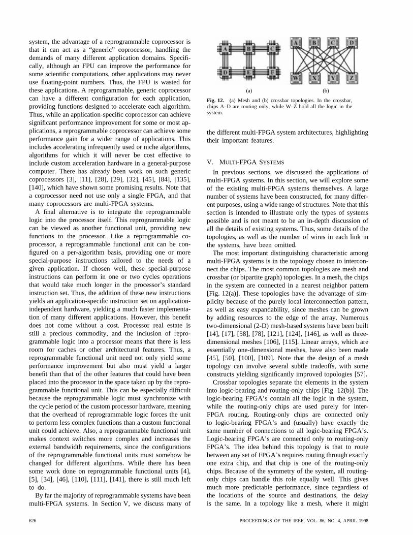
Another topology, which combines the expandability ofmeshes and the simpler routing of crossbars, is hierarchicalcrossbars [130]. As shown in Fig. 13, crossbars can bestacked together hierarchically, building up multiple levelsof routing chips. There are two simple crossbars in thesystem, one consisting of routing-only chips E–H andlogic-bearing FPGA’s M–P and a second one consistingof routing-only chips I–L and logic-bearing FPGA’s Q–T.Routing chips E–L will be called the first-level crossbars,since they connect directly to the logic-bearing FPGA’s. Tobuild the hierarchy of crossbars, the simple crossbars in thesystem can be thought of as logic-bearing chips in an evenlarger crossbar. That is, a new crossbar is built with routing-only chips and logic-bearing elements, but in this crossbar,the logic-bearing elements are complete, simple crossbars.Note that the connections within this higher level crossbargo to the routing-only chips in the simple crossbars, sofirst- and second-level routing-only chips are connectedtogether. This hierarchy can be continued, building up othercrossbars with third-level and higher routing-only chips. Inan -level hierarchical crossbar, the chips are arranged asabove, with routing-only chips at theth level connected to
chips at the th and th level, where the zerothlevel is the logic-bearing chips. Note that in contrast tothe simple crossbar topology, in a hierarchical crossbar, thelogic-bearing FPGA’s are not connected to all the routing-only chips (even those at the first level). Full connectivityoccurs at the top ( th) level, where all th-level routingchips are connected to all th level routing chips.
Routing between two logic-bearing FPGA’s in the systemsimply requires determining the level at which the sourceand destination share an ancestor, and then routing fromthe source up to one of these shared ancestors and down tothe destination. The routing from the source to the sharedancestor requires routing through exactly one routing-onlychip in each of the intervening levels, as does the routingfrom the ancestor to the destination. Because of the sym-metry of the topology, any of the ancestors of the source(for the route up) or destination (for the route down) at agiven level can be used to handle the routing, regardless ofwhat other chips are part of the route.
As mentioned earlier, the advantage of a hierarchicalcrossbar topology is that it has much of the expandabilityof a mesh, yet has much of the simplified routing ofa crossbar. Since levels of hierarchy can be added to ahierarchical crossbar, it can easily grow larger to handlebigger circuits. Levels of the hierarchy tend to map ontocomponents of the system, such as having a complete first-level crossbar on a single board, a complete second-levelcrossbar contained in a cabinet, and a complete third-level crossbar formed by interconnecting cabinets [22].The routing simplicity, as shown above, demonstrates alarge degree of flexibility in the routing paths, as well assignificant symmetry in the system. How easy it is to routebetween logic-bearing FPGA’s is simple to determine, sinceif two logic-bearing chips are within the same first-levelcrossbar, then they are as easy to route between as any otherpair of logic-bearing chips within that crossbar. Thus, whenmapping onto the topology, the system tries to keep mostof the communication between chips in the same first-levelcrossbar, most of the rest of the communication betweenchips in the same second-level crossbar, and so on.
There are two downsides to this topology. First, signalsmay have to go through many more routing-only chipsthan in a simple crossbar, since they could potentially haveto go all the way up to the top level of the hierarchy tomake a connection. The maximum routing distance is lessthan in a mesh, however, since the length in chips routedthrough of the maximum route in a mesh grows by(where is the number of logic-bearing FPGA’s in thesystem), while the length in a hierarchical crossbar growsby . The other problem is that the hierarchicalcrossbar topology requires a large number of resources toimplement the routing-only chips in the system. If one couldinstead use the routing-only chips as logic-bearing chips,the capacity of the system might be greatly increased. If thisextra logic capacity cannot efficiently be used, however, itwill be of little value.
Some systems use a two-level topology, which is some-what similar to the crossbar and hierarchical crossbar
HAUCK: FPGA’S IN REPROGRAMMABLE SYSTEMS 627
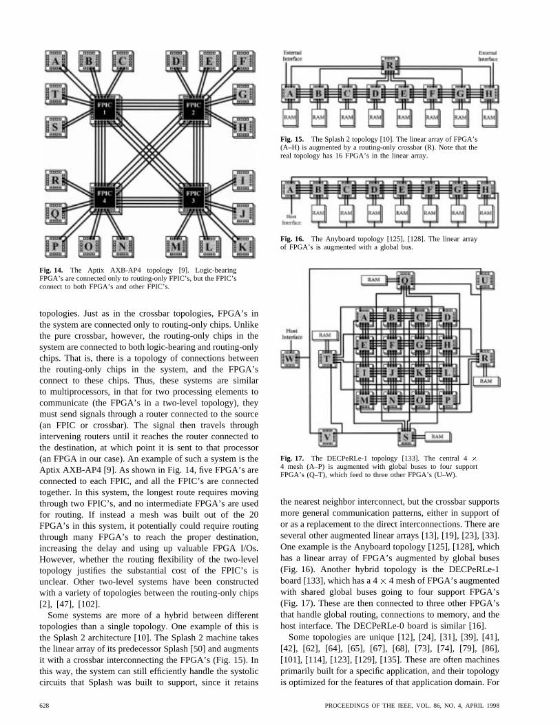
Fig. 14. The Aptix AXB-AP4 topology [9]. Logic-bearingFPGA’s are connected only to routing-only FPIC’s, but the FPIC’sconnect to both FPGA’s and other FPIC’s.
topologies. Just as in the crossbar topologies, FPGA’s inthe system are connected only to routing-only chips. Unlikethe pure crossbar, however, the routing-only chips in thesystem are connected to both logic-bearing and routing-onlychips. That is, there is a topology of connections betweenthe routing-only chips in the system, and the FPGA’sconnect to these chips. Thus, these systems are similarto multiprocessors, in that for two processing elements tocommunicate (the FPGA’s in a two-level topology), theymust send signals through a router connected to the source(an FPIC or crossbar). The signal then travels throughintervening routers until it reaches the router connected tothe destination, at which point it is sent to that processor(an FPGA in our case). An example of such a system is theAptix AXB-AP4 [9]. As shown in Fig. 14, five FPGA’s areconnected to each FPIC, and all the FPIC’s are connectedtogether. In this system, the longest route requires movingthrough two FPIC’s, and no intermediate FPGA’s are usedfor routing. If instead a mesh was built out of the 20FPGA’s in this system, it potentially could require routingthrough many FPGA’s to reach the proper destination,increasing the delay and using up valuable FPGA I/Os.However, whether the routing flexibility of the two-leveltopology justifies the substantial cost of the FPIC’s isunclear. Other two-level systems have been constructedwith a variety of topologies between the routing-only chips[2], [47], [102].
Some systems are more of a hybrid between differenttopologies than a single topology. One example of this isthe Splash 2 architecture [10]. The Splash 2 machine takesthe linear array of its predecessor Splash [50] and augmentsit with a crossbar interconnecting the FPGA’s (Fig. 15). Inthis way, the system can still efficiently handle the systoliccircuits that Splash was built to support, since it retains
Fig. 15. The Splash 2 topology [10]. The linear array of FPGA’s(A–H) is augmented by a routing-only crossbar (R). Note that thereal topology has 16 FPGA’s in the linear array.
Fig. 16. The Anyboard topology [125], [128]. The linear arrayof FPGA’s is augmented with a global bus.
Fig. 17. The DECPeRLe-1 topology [133]. The central 4�4 mesh (A–P) is augmented with global buses to four supportFPGA’s (Q–T), which feed to three other FPGA’s (U–W).
the nearest neighbor interconnect, but the crossbar supportsmore general communication patterns, either in support ofor as a replacement to the direct interconnections. There areseveral other augmented linear arrays [13], [19], [23], [33].One example is the Anyboard topology [125], [128], whichhas a linear array of FPGA’s augmented by global buses(Fig. 16). Another hybrid topology is the DECPeRLe-1board [133], which has a 4 4 mesh of FPGA’s augmentedwith shared global buses going to four support FPGA’s(Fig. 17). These are then connected to three other FPGA’sthat handle global routing, connections to memory, and thehost interface. The DECPeRLe-0 board is similar [16].
Some topologies are unique [12], [24], [31], [39], [41],[42], [62], [64], [65], [67], [68], [73], [74], [79], [86],[101], [114], [123], [129], [135]. These are often machinesprimarily built for a specific application, and their topologyis optimized for the features of that application domain. For
628 PROCEEDINGS OF THE IEEE, VOL. 86, NO. 4, APRIL 1998
Fig. 18. The Marc-1 topology [86]. The complete topology con-sists of two copies of the left subsystem (A–I, Memory, and FPU)and one copy of the right (1–5). Numbers by themselves indicateconnections to the FPGA’s at right.
example, the Marc-1 (Fig. 18) [86] is a pair of 33 meshesof FPGA’s (A–I), where most of the mesh connections linkup to a set of FPGA’s intended to be used as crossbars(1–5). While the vertical links are nearest neighbor, the hor-izontal links are actually buses. There is a complex memorysystem attached to some of the FPGA’s in the system, aswell as a floating-point unit. This machine architecture wasconstructed for a specific application—circuit simulation(and other algorithms) where the program to be executedcan be optimized on a per-run basis for values constantwithin that run, but which may vary from data set to dataset. For example, during circuit simulation, the structureof the gates in the circuit is fixed once the program beginsexecuting but can be different for each run of the simulator.Thus, if the simulator can be custom compiled on a per-runbasis for the structure of the circuit being simulated, thereis the potential for significant speedups. Because of therestricted domain of compiled-code execution, the topologywas built to contain a special-purpose processor, with theinstruction unit in FPGA’s A–C, and the data path in theFPGA’s D–I.
Another example of a system optimized for a specifictask is the RM-nc system [42]. As shown in Fig. 19, thesystem has a controller chip A, and two linear arrays ofFPGA’s B–E and F–I. Each FPGA has a local memory forbuffering data. The system contains three major buses, withthe outside buses going to only one linear array each, whilethe center bus is shared by all FPGA’s in the system. Thissystem is optimized for neural-network simulation, withthe controller chip handling global control and sequencing,while the FPGA’s in the linear array handle the individualneuron computations. A similar system for neural-networksimulation, with buses going to all FPGA’s in the systemand with no direct connections between neighbors, has alsobeen built [40].
One of the most common domains for the developmentof a custom multi-FPGA system is the prototyping ofcomputers. A good example of this is the Mushroomsystem [137], which is a system of FPGA’s, memories,
Fig. 19. The RM-nc system [42]. The linear arrays can be grownlarger than the system shown.
Fig. 20. System similar to the Mushroom processor prototypingsystem [137].
and computation chips meant to be used for processorprototyping (the exact interconnection pattern is unavail-able, but an approximate version is shown in Fig. 20).Seven FPGA’s are included in the system, and each ofthese has a specific role. FPGA A is a cache controller,B and C serve as a VMEbus interface, D handles registeraccesses, E is for processor control, F performs instructionfetches, and G is for tag manipulation and checking. Mem-ories are included for caches and the register file, whilearithmetic logical unit (ALU) and FPU chips are presentfor arithmetic operations. The advantage of this systemis that the FPGA’s can be reprogrammed to implementdifferent functions, allowing different processor structuresto be explored. The arithmetic functions and memory,features that are inefficient to implement in FPGA’s andare standard across most processors, are implemented effi-ciently in chips designed specifically for these applications.Other systems have adopted a similar approach, includinganother system intended for developing application-specificprocessors [142], a workstation design with FPGA’s forI/O functions and coprocessor development [63], and amultiprocessor system with FPGA-based cache controllersfor exploring different multiprocessor systems and cachingpolicies [104]. A somewhat related system is the CM-2X[32], a standard CM-2 supercomputer with the floating-point unit replaced with a Xilinx FPGA. This systemallows custom coprocessors to be built on a per-algorithmbasis, yielding significant performance increases for somenonfloating-point intensive programs.
There are important features of multi-FPGA systemsbeyond just the interconnect topology. One of these is
HAUCK: FPGA’S IN REPROGRAMMABLE SYSTEMS 629
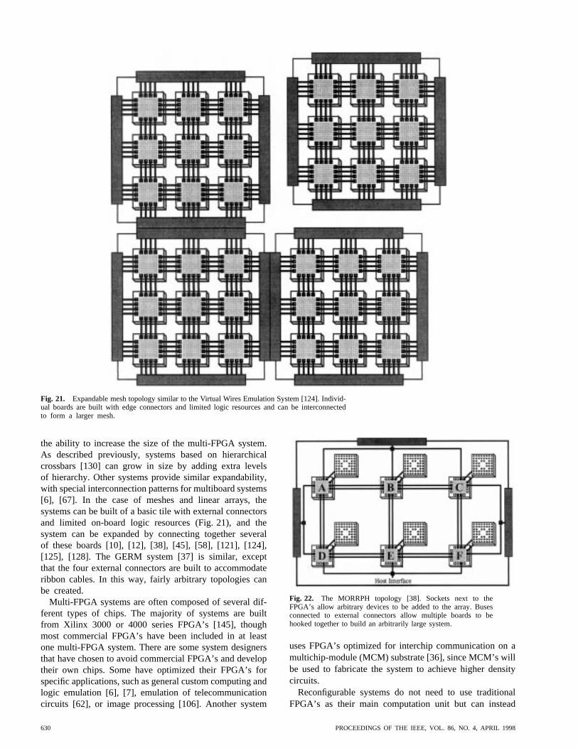
Fig. 21. Expandable mesh topology similar to the Virtual Wires Emulation System [124]. Individ-ual boards are built with edge connectors and limited logic resources and can be interconnectedto form a larger mesh.
the ability to increase the size of the multi-FPGA system.As described previously, systems based on hierarchicalcrossbars [130] can grow in size by adding extra levelsof hierarchy. Other systems provide similar expandability,with special interconnection patterns for multiboard systems[6], [67]. In the case of meshes and linear arrays, thesystems can be built of a basic tile with external connectorsand limited on-board logic resources (Fig. 21), and thesystem can be expanded by connecting together severalof these boards [10], [12], [38], [45], [58], [121], [124],[125], [128]. The GERM system [37] is similar, exceptthat the four external connectors are built to accommodateribbon cables. In this way, fairly arbitrary topologies canbe created.
Multi-FPGA systems are often composed of several dif-ferent types of chips. The majority of systems are builtfrom Xilinx 3000 or 4000 series FPGA’s [145], thoughmost commercial FPGA’s have been included in at leastone multi-FPGA system. There are some system designersthat have chosen to avoid commercial FPGA’s and developtheir own chips. Some have optimized their FPGA’s forspecific applications, such as general custom computing andlogic emulation [6], [7], emulation of telecommunicationcircuits [62], or image processing [106]. Another system
Fig. 22. The MORRPH topology [38]. Sockets next to theFPGA’s allow arbitrary devices to be added to the array. Busesconnected to external connectors allow multiple boards to behooked together to build an arbitrarily large system.
uses FPGA’s optimized for interchip communication on amultichip-module (MCM) substrate [36], since MCM’s willbe used to fabricate the system to achieve higher densitycircuits.
Reconfigurable systems do not need to use traditionalFPGA’s as their main computation unit but can instead
630 PROCEEDINGS OF THE IEEE, VOL. 86, NO. 4, APRIL 1998
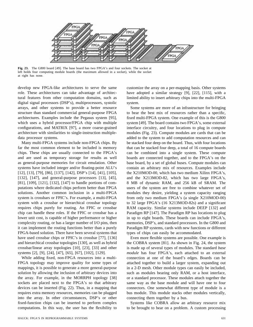
Fig. 23. The G800 board [49]. The base board has two FPGA’s and four sockets. The socket atleft holds four computing module boards (the maximum allowed in a socket), while the socketat right has none.
develop new FPGA-like architectures to serve the samerole. These architectures can take advantage of architec-tural features from other computation domains, such asdigital signal processors (DSP’s), multiprocessors, systolicarrays, and other systems to provide a better resourcestructure than standard commercial general-purpose FPGAarchitectures. Examples include the Pegasus system [95],which uses a hybrid processor/FPGA chip with multipleconfigurations, and MATRIX [97], a more coarse-grainedarchitecture with similarities to single-instruction multiple-data processor systems.
Many multi-FPGA systems include non-FPGA chips. Byfar the most common element to be included is memorychips. These chips are usually connected to the FPGA’sand are used as temporary storage for results as wellas general-purpose memories for circuit emulation. Othersystems have included integer and/or floating-point ALU’s[12], [13], [79], [86], [137], [142], DSP’s [14], [41], [105],[132], [147], and general-purpose processors [13], [45],[81], [109], [121], [132], [147] to handle portions of com-putations where dedicated chips perform better than FPGAsolutions. Another common inclusion in a multi-FPGAsystem is crossbars or FPIC’s. For example, a multi-FPGAsystem with a crossbar or hierarchical crossbar topologyrequires chips purely for routing. An FPIC or crossbarchip can handle these roles. If the FPIC or crossbar has alower unit cost, is capable of higher performance or highercomplexity routing, or has a larger number of I/O pins, thenit can implement the routing functions better than a purelyFPGA-based solution. There have been several systems thathave used crossbar chips or FPIC’s in crossbar [77], [136]and hierarchical crossbar topologies [130], as well as hybridcrossbar/linear array topologies [10], [23], [33] and othersystems [2], [9], [24], [47], [65], [67], [102], [129].
While adding fixed, non-FPGA resources into a multi-FPGA topology may improve quality for some types ofmappings, it is possible to generate a more general-purposesolution by allowing the inclusion of arbitrary devices intothe array. For example, in the MORRPH topology [38]sockets are placed next to the FPGA’s so that arbitrarydevices can be inserted (Fig. 22). Thus, in a mapping thatrequires extra memory resources, memories can be pluggedinto the array. In other circumstances, DSP’s or otherfixed-function chips can be inserted to perform complexcomputations. In this way, the user has the flexibility to
customize the array on a per-mapping basis. Other systemshave adopted a similar strategy [9], [22], [115], with alimited ability to insert arbitrary chips into the multi-FPGAsystem.
Some systems are more of an infrastructure for bringingto bear the best mix of resources rather than a specific,fixed multi-FPGA system. One example of this is the G800system [49]. The board contains two FPGA’s, some externalinterface circuitry, and four locations to plug in computemodules (Fig. 23). Compute modules are cards that can beadded to the system to add computation resources and canbe stacked four deep on the board. Thus, with four locationsthat can be stacked four deep, a total of 16 compute boardscan be combined into a single system. These computeboards are connected together, and to the FPGA’s on thebase board, by a set of global buses. Compute modules cancontain an arbitrary mix of resources. Examples includethe X210MOD-00, which has two medium Xilinx FPGA’s,and the X213MOD-82, which has two large FPGA’s,8 MB of dynamic RAM, and 256 kB of SRAM. Theusers of the system are free to combine whatever set ofmodules they desire, yielding a system capacity rangingfrom only two medium FPGA’s (a single X210MOD-00)to 32 large FPGA’s (16 X213MOD-82s) and a significantRAM capacity. Similar systems include DEEP [132] andParadigm RP [147]. The Paradigm RP has locations to plugin up to eight boards. These boards can include FPGA’s,memories, DSP’s, and standard processors. In the G800 andParadigm RP systems, cards with new functions or differenttypes of chips can easily be accommodated.
Even more flexible systems are possible. One example isthe COBRA system [81]. As shown in Fig. 24, the systemis made up of several types of modules. The standardbasemodule has four FPGA’s, each attached to an externalconnection at one of the board’s edges. Boards can beattached together to build a larger system, expanding outin a 2-D mesh. Other module types can easily be included,such as modules bearing only RAM, or a host interface,or a standard processor. These modules attach together thesame way as the base module and will have one to fourconnectors. One somewhat different type of module is abus module. This module stacks other modules vertically,connecting them together by a bus.
Systems like COBRA allow an arbitrary resource mixto be brought to bear on a problem. A custom processing
HAUCK: FPGA’S IN REPROGRAMMABLE SYSTEMS 631
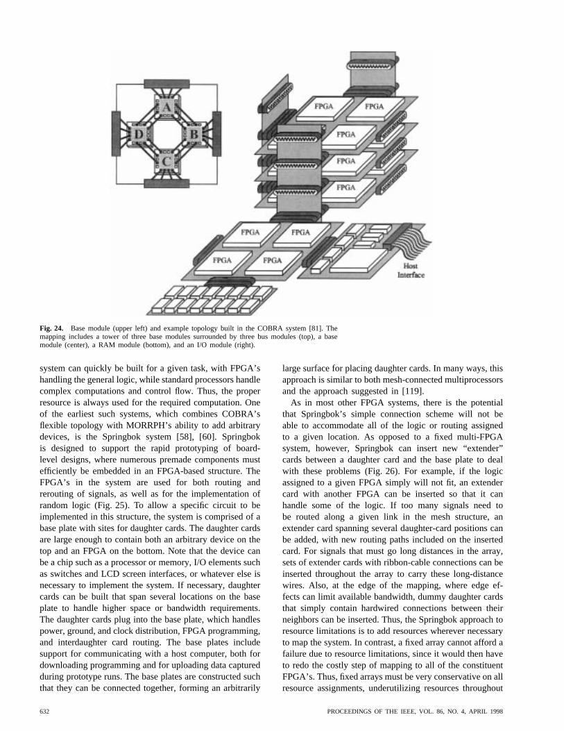
Fig. 24. Base module (upper left) and example topology built in the COBRA system [81]. Themapping includes a tower of three base modules surrounded by three bus modules (top), a basemodule (center), a RAM module (bottom), and an I/O module (right).
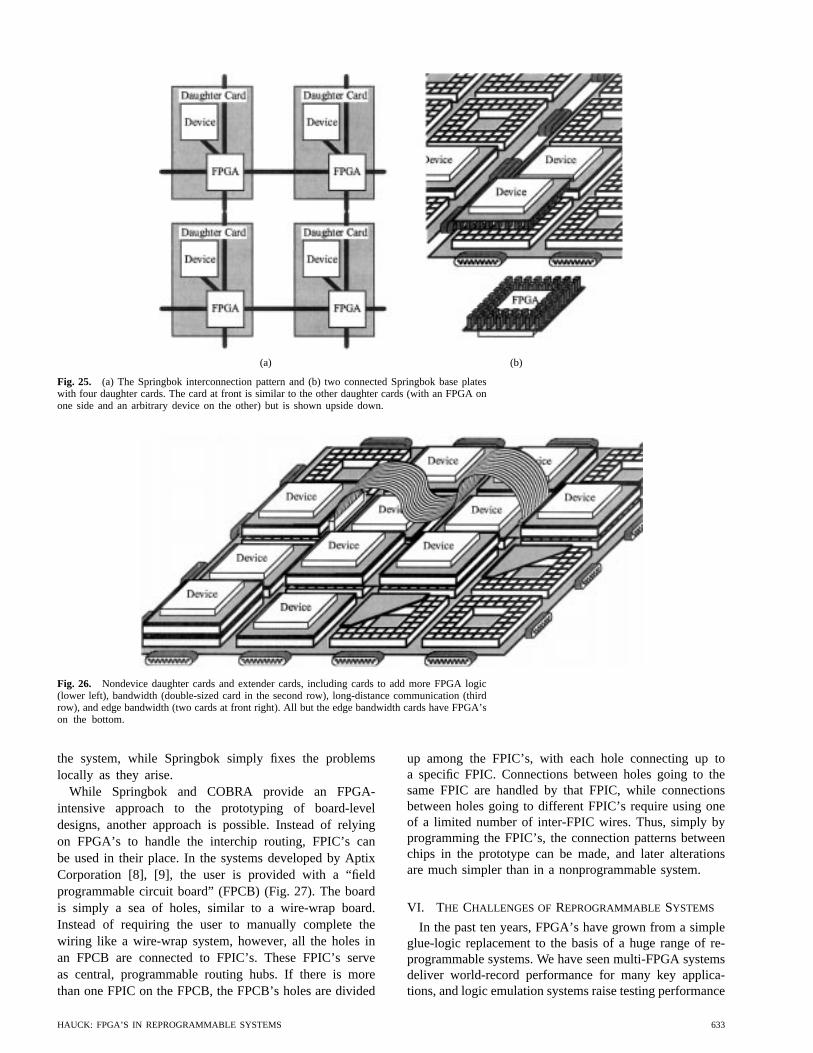
system can quickly be built for a given task, with FPGA’shandling the general logic, while standard processors handlecomplex computations and control flow. Thus, the properresource is always used for the required computation. Oneof the earliest such systems, which combines COBRA’sflexible topology with MORRPH’s ability to add arbitrarydevices, is the Springbok system [58], [60]. Springbokis designed to support the rapid prototyping of board-level designs, where numerous premade components mustefficiently be embedded in an FPGA-based structure. TheFPGA’s in the system are used for both routing andrerouting of signals, as well as for the implementation ofrandom logic (Fig. 25). To allow a specific circuit to beimplemented in this structure, the system is comprised of abase plate with sites for daughter cards. The daughter cardsare large enough to contain both an arbitrary device on thetop and an FPGA on the bottom. Note that the device canbe a chip such as a processor or memory, I/O elements suchas switches and LCD screen interfaces, or whatever else isnecessary to implement the system. If necessary, daughtercards can be built that span several locations on the baseplate to handle higher space or bandwidth requirements.The daughter cards plug into the base plate, which handlespower, ground, and clock distribution, FPGA programming,and interdaughter card routing. The base plates includesupport for communicating with a host computer, both fordownloading programming and for uploading data capturedduring prototype runs. The base plates are constructed suchthat they can be connected together, forming an arbitrarily
large surface for placing daughter cards. In many ways, thisapproach is similar to both mesh-connected multiprocessorsand the approach suggested in [119].
As in most other FPGA systems, there is the potentialthat Springbok’s simple connection scheme will not beable to accommodate all of the logic or routing assignedto a given location. As opposed to a fixed multi-FPGAsystem, however, Springbok can insert new “extender”cards between a daughter card and the base plate to dealwith these problems (Fig. 26). For example, if the logicassigned to a given FPGA simply will not fit, an extendercard with another FPGA can be inserted so that it canhandle some of the logic. If too many signals need tobe routed along a given link in the mesh structure, anextender card spanning several daughter-card positions canbe added, with new routing paths included on the insertedcard. For signals that must go long distances in the array,sets of extender cards with ribbon-cable connections can beinserted throughout the array to carry these long-distancewires. Also, at the edge of the mapping, where edge ef-fects can limit available bandwidth, dummy daughter cardsthat simply contain hardwired connections between theirneighbors can be inserted. Thus, the Springbok approach toresource limitations is to add resources wherever necessaryto map the system. In contrast, a fixed array cannot afford afailure due to resource limitations, since it would then haveto redo the costly step of mapping to all of the constituentFPGA’s. Thus, fixed arrays must be very conservative on allresource assignments, underutilizing resources throughout
632 PROCEEDINGS OF THE IEEE, VOL. 86, NO. 4, APRIL 1998
(a) (b)
Fig. 25. (a) The Springbok interconnection pattern and (b) two connected Springbok base plateswith four daughter cards. The card at front is similar to the other daughter cards (with an FPGA onone side and an arbitrary device on the other) but is shown upside down.
Fig. 26. Nondevice daughter cards and extender cards, including cards to add more FPGA logic(lower left), bandwidth (double-sized card in the second row), long-distance communication (thirdrow), and edge bandwidth (two cards at front right). All but the edge bandwidth cards have FPGA’son the bottom.
the system, while Springbok simply fixes the problemslocally as they arise.
While Springbok and COBRA provide an FPGA-intensive approach to the prototyping of board-leveldesigns, another approach is possible. Instead of relyingon FPGA’s to handle the interchip routing, FPIC’s canbe used in their place. In the systems developed by AptixCorporation [8], [9], the user is provided with a “fieldprogrammable circuit board” (FPCB) (Fig. 27). The boardis simply a sea of holes, similar to a wire-wrap board.Instead of requiring the user to manually complete thewiring like a wire-wrap system, however, all the holes inan FPCB are connected to FPIC’s. These FPIC’s serveas central, programmable routing hubs. If there is morethan one FPIC on the FPCB, the FPCB’s holes are divided
up among the FPIC’s, with each hole connecting up toa specific FPIC. Connections between holes going to thesame FPIC are handled by that FPIC, while connectionsbetween holes going to different FPIC’s require using oneof a limited number of inter-FPIC wires. Thus, simply byprogramming the FPIC’s, the connection patterns betweenchips in the prototype can be made, and later alterationsare much simpler than in a nonprogrammable system.
VI. THE CHALLENGES OF REPROGRAMMABLE SYSTEMS
In the past ten years, FPGA’s have grown from a simpleglue-logic replacement to the basis of a huge range of re-programmable systems. We have seen multi-FPGA systemsdeliver world-record performance for many key applica-tions, and logic emulation systems raise testing performance
HAUCK: FPGA’S IN REPROGRAMMABLE SYSTEMS 633
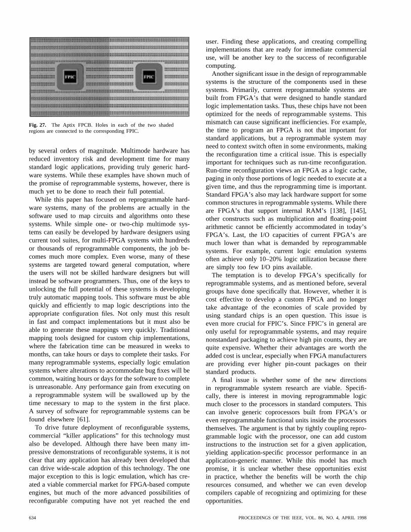
Fig. 27. The Aptix FPCB. Holes in each of the two shadedregions are connected to the corresponding FPIC.
by several orders of magnitude. Multimode hardware hasreduced inventory risk and development time for manystandard logic applications, providing truly generic hard-ware systems. While these examples have shown much ofthe promise of reprogrammable systems, however, there ismuch yet to be done to reach their full potential.
While this paper has focused on reprogrammable hard-ware systems, many of the problems are actually in thesoftware used to map circuits and algorithms onto thesesystems. While simple one- or two-chip multimode sys-tems can easily be developed by hardware designers usingcurrent tool suites, for multi-FPGA systems with hundredsor thousands of reprogrammable components, the job be-comes much more complex. Even worse, many of thesesystems are targeted toward general computation, wherethe users will not be skilled hardware designers but willinstead be software programmers. Thus, one of the keys tounlocking the full potential of these systems is developingtruly automatic mapping tools. This software must be ablequickly and efficiently to map logic descriptions into theappropriate configuration files. Not only must this resultin fast and compact implementations but it must also beable to generate these mappings very quickly. Traditionalmapping tools designed for custom chip implementations,where the fabrication time can be measured in weeks tomonths, can take hours or days to complete their tasks. Formany reprogrammable systems, especially logic emulationsystems where alterations to accommodate bug fixes will becommon, waiting hours or days for the software to completeis unreasonable. Any performance gain from executing ona reprogrammable system will be swallowed up by thetime necessary to map to the system in the first place.A survey of software for reprogrammable systems can befound elsewhere [61].
To drive future deployment of reconfigurable systems,commercial “killer applications” for this technology mustalso be developed. Although there have been many im-pressive demonstrations of reconfigurable systems, it is notclear that any application has already been developed thatcan drive wide-scale adoption of this technology. The onemajor exception to this is logic emulation, which has cre-ated a viable commercial market for FPGA-based computeengines, but much of the more advanced possibilities ofreconfigurable computing have not yet reached the end
user. Finding these applications, and creating compellingimplementations that are ready for immediate commercialuse, will be another key to the success of reconfigurablecomputing.
Another significant issue in the design of reprogrammablesystems is the structure of the components used in thesesystems. Primarily, current reprogrammable systems arebuilt from FPGA’s that were designed to handle standardlogic implementation tasks. Thus, these chips have not beenoptimized for the needs of reprogrammable systems. Thismismatch can cause significant inefficiencies. For example,the time to program an FPGA is not that important forstandard applications, but a reprogrammable system mayneed to context switch often in some environments, makingthe reconfiguration time a critical issue. This is especiallyimportant for techniques such as run-time reconfiguration.Run-time reconfiguration views an FPGA as a logic cache,paging in only those portions of logic needed to execute at agiven time, and thus the reprogramming time is important.Standard FPGA’s also may lack hardware support for somecommon structures in reprogrammable systems. While thereare FPGA’s that support internal RAM’s [138], [145],other constructs such as multiplication and floating-pointarithmetic cannot be efficiently accommodated in today’sFPGA’s. Last, the I/O capacities of current FPGA’s aremuch lower than what is demanded by reprogrammablesystems. For example, current logic emulation systemsoften achieve only 10–20% logic utilization because thereare simply too few I/O pins available.
The temptation is to develop FPGA’s specifically forreprogrammable systems, and as mentioned before, severalgroups have done specifically that. However, whether it iscost effective to develop a custom FPGA and no longertake advantage of the economies of scale provided byusing standard chips is an open question. This issue iseven more crucial for FPIC’s. Since FPIC’s in general areonly useful for reprogrammable systems, and may requirenonstandard packaging to achieve high pin counts, they arequite expensive. Whether their advantages are worth theadded cost is unclear, especially when FPGA manufacturersare providing ever higher pin-count packages on theirstandard products.
A final issue is whether some of the new directionsin reprogrammable system research are viable. Specifi-cally, there is interest in moving reprogrammable logicmuch closer to the processors in standard computers. Thiscan involve generic coprocessors built from FPGA’s oreven reprogrammable functional units inside the processorsthemselves. The argument is that by tightly coupling repro-grammable logic with the processor, one can add custominstructions to the instruction set for a given application,yielding application-specific processor performance in anapplication-generic manner. While this model has muchpromise, it is unclear whether these opportunities existin practice, whether the benefits will be worth the chipresources consumed, and whether we can even developcompilers capable of recognizing and optimizing for theseopportunities.
634 PROCEEDINGS OF THE IEEE, VOL. 86, NO. 4, APRIL 1998

VII. CONCLUSIONS
Reprogrammable systems have provided significant per-formance improvements for many types of applications.Logic emulation systems are providing orders of magnitudebetter performance than software simulation, providing“virtual prototypes” without the delays of creating true pro-totype designs. FPGA-based custom-computing machineshave achieved world-record performance for many applica-tions, providing near application-specific performance in anapplication-generic system. Last, multimode systems reducethe complexity and inventory risk for logic implementation,providing truly generic hardware systems
The hardware structures used to achieve these resultsare quite varied. Built from general-purpose FPGA’s, orperhaps even custom reprogrammable devices, they differgreatly in structure and complexity. Some are one- ortwo-chip systems providing small logic capacities. Othersare capable of expanding up to a system of hundredsor thousands of FPGA’s, providing a huge capacity forhigh-performance logic implementation. There is also greatvariation in the types of resources employed, with somesystems including memories, DSP’s, or CPU’s and otherseven allowing the user to include arbitrary devices into thesystem.
While these systems provide high-performance imple-mentations, there are several problems with today’s sys-tems. Mapping software is critical to widespread deploy-ment of these systems, yet current software is much slowerand provides lower quality than is often required. Also,current systems primarily use off-the-shelf FPGA’s, which,while providing some economies of scale, also present thesystem designer with significant inefficiencies.
There is much left to be done with reprogrammablesystems, with much promise yet to be fulfilled. Repro-grammable functional units in standard processors mayyield application-specific processors in an application-generic manner. Reprogrammable coprocessors couldbecome generic coprocessors, yielding custom acceleratorsfor arbitrary applications, including niche needs for whichcustom hardware will never be cost effective. In theseways, FPGA’s may become the cornerstone of many futurecomputation systems.
REFERENCES
[1] FPGA Data Book and Design Guide.Sunnyvale, CA: ActelCorp., 1994.
[2] J. K. Adams, H. Schmitt, and D. E. Thomas, “A model andmethodology for hardware-software codesign,” inProc. Int.Workshop Hardware-Software Codesign,1993.
[3] L. Agarwal, M. Wazlowski, and S. Ghosh, “An asynchronousapproach to efficient execution of programs on adaptive archi-tectures utilizing FPGA’s,” inProc. IEEE Workshop FPGA’sfor Custom Computing Machines,1994, pp. 101–110.
[4] O. T. Albaharna, P. Y. K. Cheung, and T. J. Clarke, “Area &time limitations of FPGA-based virtual hardware,” inProc. Int.Conf. Computer Design,1994, pp. 184–189.
[5] , “On the viability of FPGA-based integrated coproces-sors,” in Proc. IEEE Symp. FPGA’s for Custom ComputingMachines,1996, pp. 206–215.
[6] R. Amerson, R. J. Carter, W. B. Culbertson, P. Kuekes, and G.Snider, “Teramac—Configurable custom computing,” inProc.
IEEE Symp. FPGA’s for Custom Computing Machines,1995,pp. 32–38.
[7] , “Plasma: An FPGA for million gate systems,” inProc.ACM/SIGDA Int. Symp. Field Programmable Gate Arrays,1996, pp. 10–16.
[8] Data Book. San Jose, CA: Aptix Corp., 1993.[9] Data Book Supplement. San Jose, CA: Aptix Corp., 1993.
[10] J. M. Arnold, D. A. Buell, and E. G. Davis, “Splash 2,” inProc.4th Ann. ACM Symp. Parallel Algorithms and Architectures,1992, pp. 316–322.
[11] P. M. Athanas and H. F. Silverman, “Processor reconfigurationthrough instruction-set metamorphosis,”IEEE Comput. Mag.,vol. 26, no. 3, pp. 11–18, Mar. 1993
[12] P. J. Bakkes, J. J. du Plessis, and B. L. Hutchings, “Mixingfixed and reconfigurable logic for array processing,” inProc.IEEE Symp. FPGA’s for Custom Computing Machines,1996,pp. 118–125.
[13] T. Benner, R. Ernst, I. Konenkamp, U. Holtmann, P.Schuler, H.-C. Schaub, and N. Serafimov, “FPGA basedprototyping for verification and evaluation in hardware-software cosynthesis,” inLecture Notes in Computer Science849—Field-Programmable Logic: Architectures, Synthesis andApplications, R. W. Hartenstein and M. Z. Servıt, Eds. Berlin,Germany: Springer-Verlag, 1994, pp. 251–258.
[14] N. W. Bergmann and J. C. Mudge, “Comparing the performanceof FPGA-based custom computers with general-purpose com-puters for DSP applications,” inProc. IEEE Workshop FPGA’sfor Custom Computing Machines,1994, pp. 164–171.
[15] P. Bertin, D. Roncin, and J. Vuillemin, “Introduction to pro-grammable active memories,” inSystolic Array Processors,J. McCanny, J. McWhirter, and E. Swartzlander, Jr., Eds.Englewood Cliffs, NJ: Prentice-Hall, 1989, pp. 300–309.
[16] P. Bertin, “Memoires actives programmables: Conception,realization et programmation,” Ph.D. dissertation, UniversiteParis 7 Ufr d’Informatique, 1993.
[17] T. Blickle, J. Konig, and L. Thiele, “A prototyping array forparallel architectures,” inMore FPGA’s, W. R. Moore andW. Luk, Eds. Oxford, England: Abingdon EE&CS, 1994, pp.388–397.
[18] M. Bolotski, A. DeHon, and T. F. Knight, Jr., “UnifyingFPGA’s and SIMD arrays,” inProc. 2nd Int. ACM/SIGDAWorkshop Field-Programmable Gate Arrays,1994.
[19] B. Box, “Field programmable gate array based reconfigurablepreprocessor,” inProc. IEEE Workshop FPGA’s for CustomComputing Machines,1994, pp. 40–48.
[20] G. Brebner and J. Gray, “Use of reconfigurability in variable-length code detection at video rates,” inLecture Notes inComputer Science 975—Field-Programmable Logic and Appli-cations, W. Moore and W. Luk, Eds. London, U.K.: Springer,1995, pp. 429–438.
[21] S. D. Brown, R. J. Francis, J. Rose, and Z. G. Vranesic,Field-Programmable Gate Arrays.Boston, MA: Kluwer, 1992.
[22] M. Butts and J. Batcheller, “Method of using electronicallyreconfigurable logic circuits,” U.S. Patent 5 036 473, July 30,1991.
[23] J. M. Carrera, E. J. Martınez, S. A. Fernandez, and J. M. Chaus,“Architecture of a FPGA-based coprocessor: The PAR-1,” inProc. IEEE Symp. FPGA’s for Custom Computing Machines,1995, pp. 20–29.
[24] S. Casselman, “Virtual computing and the virtual computer,”in Proc. IEEE Workshop FPGA’s for Custom Computing Ma-chines,1993, pp. 43–48.
[25] P. K. Chan, M. Schlag, and M. Martin, “BORG: A reconfig-urable prototyping board using field-programmable gate arrays,”in Proc. 1st Int. ACM/SIGDA Workshop Field-ProgrammableGate Arrays,1992, pp. 47–51.
[26] P. K. Chan and S. Mourad,Digital Design Using Field Pro-grammable Gate Arrays. Englewood Cliffs, NJ: Prentice-Hall,1994.
[27] P. K. Chan, M. D. F. Schlag, and J. Y. Zien, “Spectral-basedmulti-way FPGA partitioning,” inProc. ACM/SIGDA Int. Symp.Field Programmable Gate Arrays,1995, pp. 133–139.
[28] S. Churcher, T. Kean, and B. Wilkie, “The XC6200 FastMapprocessor interface,” inLecture Notes in Computer Science975—Field-Programmable Logic and Applications, W. Mooreand W. Luk, Eds. London, U.K.: Springer, 1995, pp. 36–43.
[29] D. A. Clark and B. L. Hutchings, “Supporting FPGA micro-processors through retargetable software tools,” inProc. IEEE
HAUCK: FPGA’S IN REPROGRAMMABLE SYSTEMS 635
Symp. FPGA’s for Custom Computing Machines,1996, pp.195–203.
[30] C. P. Cowen and S. Monaghan, “A reconfigurable Monte-Carlo clustering processor (MCCP),” inProc. IEEE WorkshopFPGA’s for Custom Computing Machines,1994, pp. 59–65.
[31] C. E. Cox and W. E. Blanz, “GANGLION—A fast field-programmable gate array implementation of a connectionistclassifier,” IEEE J. Solid-State Circuits,vol. 27, pp. 288–299,Mar. 1992.
[32] S. A. Cuccaro and C. F. Reese, “The CM-2X: A hybridCM-2/Xilinx prototype,” in Proc. IEEE Workshop FPGA’s forCustom Computing Machines,1993, pp. 121–130.
[33] J. Darnauer, P. Garay, T. Isshiki, J. Ramirez, and W. W.-M.Dai, “A field programmable multi-chip module (FPMCM),”in Proc. IEEE Workshop FPGA’s for Custom Computing Ma-chines,1994, pp. 1–10.
[34] A. DeHon, “DPGA-coupled microprocessors: Commodity IC’sfor the early 21st century,” inProc. IEEE Workshop FPGA’sfor Custom Computing Machines,1994, pp. 31–39.
[35] , “DPGA utilization and application,” in Proc.ACM/SIGDA Int. Symp. Field-Programmable Gate Arrays,1996, pp. 115–121.
[36] I. Dobbelaere, A. El Gamal, D. How, and B. Kleveland, “Fieldprogrammable MCM systems—Design of an interconnectionframe,” in Proc. 1st Int. ACM/SIGDA Workshop Field Pro-grammable Gate Arrays,1992, pp. 52–56.
[37] A. Dollas, B. Ward, and J. D. S. Babcock, “FPGA basedlow cost generic reusable module for the rapid prototypingof subsystems,” in Lecture Notes in Computer Science849—Field-Programmable Logic: Architectures, Synthesis andApplications, R. W. Hartenstein and M. Z. Servıt, Eds. Berlin,Germany: Springer-Verlag, 1994, pp. 259–270.
[38] T. H. Drayer, W. E. King IV, J. G. Tront, and R. W. Con-ners, “MORRPH: A modular and reprogrammable real-timeprocessing hardware,” inProc. IEEE Symp. FPGA’s for CustomComputing Machines,1995, pp. 11–19.
[39] P. Dunn, “A configurable logic processor for machinevision,” in Lecture Notes in Computer Science 975—Field-Programmable Logic and Applications, W. Moore and W. Luk,Eds. London, U.K.: Springer, 1995, pp. 68–77.
[40] J. G. Eldredge and B. L. Hutchings, “Density enhancementof a neural network using FPGA’s and run-time reconfigura-tion,” in Proc. IEEE Workshop FPGA’s for Custom ComputingMachines,pp. 180–188, 1994.
[41] M. Engels, R. Lauwereins, and J. A. Peperstraete, “Rapidprototyping for DSP systems with microprocessors,”IEEEDesign Test Computers Mag.,pp. 52–62, June 1991.
[42] S. S. Erdogan and A. Wahab, “Design of RM-nc: A re-configurable neurocomputer for massively parallel-pipelinedcomputations,” inProc. Int. Joint Conf. Neural Networks,vol.2, 1992, pp. 33–38.
[43] B. Fawcett, “Applications of reconfigurable logic,” inMoreFPGAsj, W. R. Moore and W. Luk, Eds. Oxford, England:Abingdon EE&CS, 1994, pp. 57–69.
[44] A. Ferrucci, M. Martın, T. Geocaris, M. Schlag, and P. K. Chan,“ACME: A field-programmable gate array implementation ofa self-adapting and scalable connectionist network (extendedabstract),” in Proc. 2nd Int. ACM/SIGDA Workshop Field-Programmable Gate Arrays,1994.
[45] J. M. Filloque, C. Beaumont, and B. Pottier, “Distributedsynchronization on a parallel machine with a logic layer,” inProc. Euromicro Workshop Parallel and Distributed Computing,1993, pp. 53–58.
[46] P. C. French and R. W. Taylor, “A self-reconfiguring proces-sor,” in Proc. IEEE Workshop FPGA’s for Custom ComputingMachines,1993, pp. 50–59.
[47] D. Galloway, D. Karchmer, P. Chow, D. Lewis, and J.Rose, “The transmogrifier: The University of Toronto field-programmable system,” inProc. 2nd Canadian WorkshopField-Programmable Devices,1994.
[48] J. Gateley, “Logic emulation aids design process,”ASIC &EDA, July 1994.
[49] “G800 RIC,” Giga Operations Corp., Berkeley, CA, 1995.[50] M. Gokhale, B. Holmes, A. Kopser, D. Kunze, D. Lopresti,
S. Lucas, R. Minnich, and P. Olsen, “Splash: A reconfigurablelinear logic array,” Int. Conf. Parallel Processing,1990, pp.526–532.
[51] M. Gokhale and A. Marks, “Automatic synthesis of parallel pro-
grams targeted to dynamically reconfigurable logic arrays,” inLecture Notes in Computer Science 975—Field-ProgrammableLogic and Applications, W. Moore and W. Luk, Eds. London,U.K.: Springer, 1995, pp. 399–408.
[52] P. Graham and B. Nelson, “A hardware genetic algorithmfor the traveling salesman problem on Splash 2,” inLectureNotes in Computer Science 975—Field-Programmable Logicand Applications, W. Moore and W. Luk, Eds. London, U.K.:Springer, 1995, pp. 352–361.
[53] , “Genetic algorithms in software and in hardware—Aperformance analysis of workstation and custom computingmachine implementations,” inProc. IEEE Symp. FPGA’s forCustom Computing Machines,1996, pp. 216–225.
[54] J. Greene, E. Hamdy, and S. Beal, “Antifuse field programmablegate arrays,”Proc. IEEE,vol. 81, pp. 1042–1056, July 1993.
[55] S. A. Guccione and M. J. Gonzalez, “Classification and per-formance of reconfigurable architectures,” inLecture Notes inComputer Science 975—Field-Programmable Logic and Ap-plications, W. Moore and W. Luk, Eds. London, England:Springer, 1995, pp. 439–448.
[56] J. D. Hadley and B. L. Hutchings, “Design methodologies forpartially reconfigured systems,” inProc. IEEE Symp. FPGA’sfor Custom Computing Machines,1995, pp. 78–84.
[57] S. Hauck, G. Borriello, and C. Ebeling, “Mesh routing topolo-gies for multi-FPGA systems,” inProc. Int. Conf. ComputerDesign,Oct. 1994, pp. 170–177.
[58] , “Springbok: A rapid-prototyping system for board-level designs,” in Proc. ACM/SIGDA 2nd Int. WorkshopField-Programmable Gate Arrays,Feb. 1994.
[59] , “Achieving high-latency, low-bandwidth communication:Logic emulation interfaces,” Dept. of Computer Science andEngineering, University of Washington, Seattle, Tech. Rep.#95-04-04, Jan. 1995.
[60] S. Hauck, “Multi-FPGA systems,” Ph.D. dissertation, Dept. ofComputer Science and Engineering, University of Washington,Seattle, 1995.
[61] S. Hauck and A. Agarwal, submitted for publication.[62] K. Hayashi, T. Miyazaki, K. Shirakawa, K. Yamada, and N.
Ohta, “Reconfigurable real-time signal transport system usingcustom FPGA’s,” inProc. IEEE Symp. FPGA’s for CustomComputing Machines,1995, pp. 68–75.
[63] B. Heeb and C. Pfister, “Chameleon: A workstation ofa different color,” in Lecture Notes in Computer Science705—Field-Programmable Gate Arrays: Architectures andTools for Rapid Prototyping, H. Grunbacher and R. W.Hartenstein, Eds. Berlin, Germany: Springer-Verlag, 1993,pp. 152–161.
[64] H.-J. Herpel, N. Wehn, M. Gasteier, and M. Glesner, “Areconfigurable computer for embedded control applications,”in Proc. IEEE Workshop FPGA’s for Custom Computing Ma-chines,1993, pp. 111–120.
[65] H.-J. Herpel, U. Ober, and M. Glesner, “Prototype generation ofapplication specific embedded controllers for microsystems,” inLecture Notes in Computer Science 975—Field-ProgrammableLogic and Applications, W. Moore and W. Luk, Eds. London,England: Springer, 1995, pp. 341–351.
[66] D. T. Hoang, “Searching genetic databases on Splash 2,” inProc. IEEE Workshop FPGA’s for Custom Computing Ma-chines,1993, pp. 185–191.
[67] H. Hogl, A. Kugel, J. Ludvig, R. M¨anner, K. H. Noffz, andR. Zoz, “Enable : A second generation FPGA processor,”in Proc. IEEE Symp. FPGA’s for Custom Computing Machines,1995, pp. 45–53.
[68] N. Howard, “Defect-tolerant field-programmable gate arrays,”Ph.D. dissertation, Department of Electronics, University ofYork, U.K., 1994.
[69] N. Howard, A. Tyrrell, and N. Allinson, “FPGA accelerationof electronic design automation tasks,” inMore FPGA’s, W. R.Moore and W. Luk, Eds. Oxford, England: Abingdon EE&CS,1994, pp. 337–344.
[70] D. J.-H. Huang, and A. B. Kahng, “Multi-way system parti-tioning into a single type or multiple types of FPGA’s,” inProc. ACM/SIGDA Int. Symp. Field Programmable Gate Arrays,1995, pp. 140–145.
[71] B. L. Hutchings and M. J. Wirthlin, “Implementationapproaches for reconfigurable logic applications,” inLectureNotes in Computer Science 975—Field-Programmable Logicand Applications, W. Moore, W. Luk, Eds. London, England:
636 PROCEEDINGS OF THE IEEE, VOL. 86, NO. 4, APRIL 1998
Springer, 1995, pp. 419–428.[72] “The FPID family data sheet,” I-Cube, Inc., Santa Clara, CA,
Feb. 1994.[73] C. Iseli and E. Sanchez, “Spyder: A reconfigurable VLIW
processor using FPGA’s,” inProc. IEEE Workshop FPGA’s forCustom Computing Machines,1993, pp. 17–24.
[74] A. Jantsch, P. Ellervee, J.Oberg, and A. Hemani, “A case studyon hardware/software partitioning,” inProc. IEEE WorkshopFPGA’s for Custom Computing Machines,1994, pp. 111–118.
[75] J. H. Jenkins,Designing with FPGA’s and CPLD’s. Engle-wood Cliffs, NJ: Prentice-Hall, 1994.
[76] C. Jones, J. Oswald, B. Schoner, and J. Villasenor, “Issues inwireless video coding using run-time-reconfigurable FPGA’s,”in Proc. IEEE Symp. FPGA’s for Custom Computing Machines,1995, pp. 85–89.
[77] M. Slimane-Kadi, D. Brasen, and G. Saucier, “A fast-FPGAprototyping system that uses inexpensive high-performanceFPIC,” in Proc. ACM/SIGDA Workshop Field-ProgrammableGate Arrays,1994.
[78] T. Kean and I. Buchanan, “The use of FPGA’s in a novelcomputing subsystem,” inProc. 1st Int. ACM/SIGDA WorkshopField-Programmable Gate Arrays,1992, pp. 60–66.
[79] G. Knittel, “A PCI-compatible FPGA-coprocessor for 2D/3Dimage processing,” inProc. IEEE Symp. FPGA’s for CustomComputing Machines,1996, pp. 136–145.
[80] A. Koch and U. Golze, “A universal co-processor for work-stations,” in More FPGA’s, W. R. Moore and W. Luk, Eds.Oxford, England: Abingdon EE&CS, 1994, pp. 317–328.
[81] G. Koch, U. Kebschull, and W. Rosenstiel, “A prototypingenvironment for hardware/software codesign in the COBRAproject,” in Proc. 3rd Int. Workshop Hardware/Software Code-sign, Sept. 1994.
[82] R. Kuznar, F. Brglez, and K. Kozminski, “Cost minimizationof partitions into multiple devices,” inProc. Design AutomationConf., 1993, pp. 315–320.
[83] R. Kuznar, F. Brglez, and B. Zajc, “Multi-way netlist partition-ing into heterogeneous FPGA’s and minimization of total devicecost and interconnect,” inProc. Design Automation Conf., 1994,pp. 238–243.
[84] A. Lawrence, A. Kay, W. Luk, T. Nomura, and I. Page,“Using reconfigurable hardware to speed up product develop-ment and performance,” inLecture Notes in Computer Science975—Field-Programmable Logic and Applications. W. Mooreand W. Luk, Eds. London, England: Springer, 1995, pp.111–118.
[85] E. Lemoine and D. Merceron, “Run time reconfiguration ofFPGA for scanning genomic databases,” inProc. IEEE Symp.FPGA’s for Custom Computing Machines,1995, pp. 90–98.
[86] D. M. Lewis, M. H. van Ierssel, and D. H. Wong, “A fieldprogrammable accelerator for compiled-code applications,” inProc. ICCD ’93, 1993, pp. 491–496.
[87] J. Li and C.-K. Cheng, “Routability improvement using dy-namic interconnect architecture,” inProc. IEEE Symp. FPGA’sfor Custom Computing Machines,1995, pp. 61–67.
[88] X.-P. Ling and H. Amano, “WASMII: A data driven computeron a virtual hardware,” inProc. IEEE Workshop FPGA’s forCustom Computing Machines,1993, pp. 33–42.
[89] D. P. Lopresti, “Rapid implementation of a genetic sequencecomparator using field-programmable logic arrays,” inProc.Advanced Research in VLSI 1991: Santa Cruz,pp. 139–152.
[90] W. Luk, N. Shirazi, and P. Y. K. Cheung, “Modeling andoptimising run-time reconfigurable systems,” inProc. IEEESymp. FPGA’s for Custom Computing Machines,1996, pp.167–176.
[91] P. Lysaght, “Dynamically reconfigurable logic in undergraduateprojects,” inFPGA’s, W. Moore and W. Luk, Eds. Abingdon,England: Abingdon EE&CS, 1991, pp. 424–436.
[92] P. Lysaght and J. Dunlop, “Dynamic reconfiguration ofFPGA’s,” in More FPGA’s, W. R. Moore and W. Luk, Eds.Oxford, England: Abingdon EE&CS, 1994, pp. 82–94.
[93] P. Lysaght, J. Stockwood, J. Law, and D. Girma, “Artificialneural network implementation on a fine-grained FPGA,” inLecture Notes in Computer Science 849—Field-ProgrammableLogic: Architectures, Synthesis and Applications, R. W. Harten-stein and M. Z. Servıt, Eds. Berlin, Germany: Springer-Verlag,1994, pp. 421–431.
[94] P. Lysaght, H. Dick, G. McGregor, D. McConnell, andJ. Stockwood, “Prototyping environment for dynamically
reconfigurable logic,” inLecture Notes in Computer Science975—Field-Programmable Logic and Applications, W. Mooreand W. Luk, Eds. London, England: Springer, 1995, pp.409–418.
[95] L. Maliniak, “Hardware emulation draws speed from innovative3D parallel processing based on custom IC’s,”Electron. Design,May 30, 1994.
[96] J. Mayrhofer and J. Strachwitz, “A control circuit for electricaldrives based on transputers and FPGA’s,” inMore FPGA’s, W.R. Moore, W. Luk, Eds. Oxford, England: Abingdon EE&CS,1994, pp. 420–427.
[97] E. Mirsky and A. DeHon, “MATRIX: A reconfigurable comput-ing architecture with configurable instruction distribution anddeployable resources,” inProc. IEEE Symp. FPGA’s for CustomComputing Machines,1996, pp. 157–166.
[98] L. Moll, J. Vuillemin, and P. Boucard, “High-energy physicson DECPeRLe-1 programmable active memory,” inProc.ACM/SIGDA Int. Symp. Field-Programmable Gate Arrays,1995, pp. 47–52.
[99] S. Monaghan and C. P. Cowen, “Reconfigurable multi-bit pro-cessor for DSP applications in statistical physics,” inProc. IEEEWorkshop FPGA’s for Custom Computing Machines,1993, pp.103–110.
[100] S. Monaghan and J. E. Istiyanto, “High-level hardware synthesisfor large scale computational physics targeted at FPGA’s,”in More FPGA’s, W. R. Moore and W. Luk, Eds. Oxford,England: Abingdon EE&CS, 1994, pp. 238–248.
[101] R. Nguyen and P. Nguyen, “FPGA based reconfigurable ar-chitecture for a compact vision system,” inLecture Notes inComputer Science 849—Field-Programmable Logic: Architec-tures, Synthesis and Applications, R. W. Hartenstein and M.Z. Servıt, Eds., Berlin, Germany: Springer-Verlag, 1994, pp.141–143.
[102] T. Njølstad, J. Pihl, and J. Hofstad, “ZAREPTA: A zero lead-time, all reconfigurable system for emulation, prototyping andtesting of ASIC’s,” in Lecture Notes in Computer Science849—Field-Programmable Logic: Architectures, Synthesis andApplications, R. W. Hartenstein and M. Z. Servıt, Eds. Berlin,Germany: Springer-Verlag, 1994, pp. 230–239.
[103] J. V. Oldfield and R. C. Dorf, Eds.,Field ProgrammableGate Arrays: Reconfigurable Logic for Rapid Prototyping andImplementation of Digital Systems.New York: Wiley, 1995.
[104] K. Oner, L. A. Barroso, S. Iman, J. Jeong, K. Ramamurthy,and M. Dubois, “The design of RPM: An FPGA-based mul-tiprocessor emulator,” inProc. ACM/SIGDA Int. Symp. Field-Programmable Gate Arrays,1995, pp. 60–66.
[105] H. Pottinger, W. Eatherton, J. Kelly, T, Schiefelbein, L.R. Mullin, and R. Ziegler, “Hardware assists for highperformance computing using a mathematics of arrays,” inProc.ACM/SIGDA Int. Symp. Field-Programmable Gate Arrays,1995, pp. 39–45.
[106] G. M. Quenot, I. C. Kraljic, J. Serot, and B. Zavidovique, “Areconfigurable compute engine for real-time vision automataprototyping,” in Proc. IEEE Workshop FPGA’s for CustomComputing Machines,1994, pp. 91–100.
[107] “Picasso graphics emulator adapter,” Quickturn Design Sys-tems, Inc., Mountain View, CA, 1993.
[108] R. V. Rachakonda, “High-speed region detection and label-ing using an FPGA-based custom computing platform,” inLecture Notes in Computer Science 975—Field-ProgrammableLogic and Applications, W. Moore and W. Luk, Eds. London,England: Springer, 1995, pp. 86–93.
[109] F. Raimbault, D. Lavenier, S. Rubini, and B. Pottier, “Fine grainparallelism on a MIMD machine using FPGA’s,” inProc. IEEEWorkshop FPGA’s for Custom Computing Machines,1993, pp.2–8.
[110] S. Rajamani and P. Viswanath, “A quantitative analysis of pro-cessor—Programmable logic interface,” inProc. IEEE Symp.FPGA’s for Custom Computing Machines,1996, pp. 226–234.
[111] R. Razdan and M. D. Smith, “A high-performance microarchi-tecture with hardware-programmable functional units,” inProc.Int. Symp. Microarchitecture,1994, pp. 172–180.
[112] J. Rose, A. El Gamal, and A. Sangiovanni-Vincentelli, “Ar-chitecture of field-programmable gate arrays,”Proc. IEEE,vol.81, pp. 1013–1029, July 1993.
[113] D. Ross, O. Vellacotta, and M. Turner, “An FPGA-basedhardware accelerator for image processing,” inMore FPGA’s,W. R. Moore and W. Luk, Eds. Oxford, England: Abingdon
HAUCK: FPGA’S IN REPROGRAMMABLE SYSTEMS 637
EE&CS, 1994, pp. 299–306.[114] T. Saluvere, D. Kerek, and H. Tenhunen, “Direct se-
quence spread spectrum digital radio DSP prototyping usingXilinx FPGA’s,” in Lecture Notes in Computer Science849—Field-Programmable Logic: Architectures, Synthesis andApplications, R. W. Hartenstein and M. Z. Servıt, Eds. Berlin,Germany: Springer-Verlag, 1994, pp. 138–140.
[115] S. P. Sample, M. R. D’Amour, and T. S. Payne, “Apparatusfor emulation of electronic hardware system,” U.S. Patent5 109 353, Apr. 28, 1992.
[116] H. Schmit and D. Thomas, “Hidden Markov modeling andfuzzy controllers in FPGA’s,” inProc. IEEE Symp. FPGA’sfor Custom Computing Machines,1995, pp. 214–221.
[117] B. Schoner, C. Jones, and J. Villasenor, “Issues in wirelessvideo coding using run-time-reconfigurable FPGA’s,” inProc.IEEE Symp. FPGA’s for Custom Computing Machines,1995,pp. 85–89.
[118] S. D. Scott, A. Samal, and S. Seth, “HGA: A hardware-basedgenetic algorithm,” inProc. ACM/SIGDA Int. Symp. Field-Programmable Gate Arrays,pp. 53–59, 1995.
[119] C. L. Seitz, “Let’s route packets instead of wires,” inAdvancedResearch in VLSI: Proc. 6th MIT Conf.,1990, pp. 133–138.
[120] M. Shand, “Flexible image acquisition using reconfigurablehardware,” inProc. IEEE Symp. FPGA’s for Custom ComputingMachines,1995, pp. 125–134.
[121] P. Shaw and G. Milne, “A highly parallel FPGA-based machineand its formal verification,” inLecture Notes in Computer Sci-ence 705—Field-Programmable Gate Arrays: Architectures andTools for Rapid Prototyping,H. Grunbacher, R. W. Hartenstein,Eds. Berlin, Germany: Springer-Verlag, 1993, pp. 162–173.
[122] S. Singh and P. Bellec, “Virtual hardware for graphics appli-cations using FPGA’s,” inProc. IEEE Workshop FPGA’s forCustom Computing Machines,1994, pp. 49–58.
[123] N. Suganuma, Y. Murata, S. Nakata, S. Nagata, M. Tomita,and K. Hirano, “Reconfigurable machine and its application tologic diagnosis,” inProc. Int. Conf. Computer-Aided Design,1992, pp. 373–376.
[124] R. Tessier, J. Babb, M. Dahl, S. Hanono, and A. Agarwal, “Thevirtual wires emulation system: A gate-efficient ASIC proto-typing environment,” inProc. 2nd Int. ACM/SIGDA WorkshopField-Programmable Gate Arrays,1994.
[125] D. A. Thomae, T. A. Petersen, and D. E. Van den Bout, “TheAnyboard rapid prototyping environment,” inProc. AdvancedResearch in VLSI 1991: Santa Cruz,1991, pp. 356–370.
[126] S. Trimberger, “A reprogrammable gate array and applications,”Proc. IEEE,vol. 81, pp. 1030–1041, July 1993.
[127] , Field-Programmable Gate Array Technology.Boston,MA: Kluwer, 1994.
[128] D. E. Van den Bout, J. N. Morris, D. Thomae, S. Labrozzi,S. Wingo, and D. Hallman, “Anyboard: An FPGA-based, re-configurable system,”IEEE Design Test Computers Mag.,Sept.1992, pp. 21–30.
[129] D. E. Van den Bout, “The XESS RIPP board,” inField-Programmable Gate Arrays: Reconfigurable Logic for RapidPrototyping and Implementation of Digital Systems,J. V. Old-field and R. C. Dorf, Eds. New York: Wiley, 1995, pp.309–312.
[130] J. Varghese, M. Butts, and J. Batcheller, “An efficient logicemulation system,”IEEE Trans. VLSI Syst.,vol. 1, pp. 171–174,June 1993.
[131] J. Villasenor, B. Schoner, K.-N. Chia, and C. Zapata, “Config-urable computing solutions for automatic target recognition,”in Proc. IEEE Symp. FPGA’s for Custom Computing Machines,1996, pp. 70–79.
[132] G. vom Bogel, P. Nauber, and J. Winkler, “A design envi-ronment with emulation of prototypes for hardware/softwaresystems using XILINX FPGA,” inLecture Notes in ComputerScience 849—Field-Programmable Logic: Architectures, Syn-
thesis and Applications, R. W. Hartenstein and M. Z. Serv´ıt,Eds. Berlin, Germany: Springer-Verlag, 1994, pp. 315–317.
[133] J. Vuillemin, P. Bertin, D. Roncin, M. Shand, H. Touati, andP. Boucard, “Programmable active memories: Reconfigurablesystems come of age,”IEEE Trans. VLSI Syst.,vol. 4, pp.56–69, Mar. 1996.
[134] J. F. Wakerly,Digital Design: Principles and Practices.En-glewood Cliffs, NJ: Prentice-Hall, 1994.
[135] M. Wazlowski, L. Agarwal, T. Lee, A. Smith, E. Lam, P.Athanas, H. Silverman, and S. Ghosh, “PRISM-II compilerand architecture,” inProc. IEEE Workshop FPGA’s for CustomComputing Machines,1993, pp. 9–16.
[136] R. Weiss, “MCM 4 FPGA’s 50,000 gates, 4048 flip-flops,”EDN Mag.,p. 116, Apr. 28, 1994.
[137] I. Williams, “Using FPGA’s to prototype new computer archi-tectures,” inFPGA’s, W. Moore, W. Luk, Eds. Abingdon,England: Abingdon EE&CS, 1991, pp. 373–382.
[138] S. J. E. Wilton, J. Rose, and Z. G. Vranesic, “Architecture ofcentralized field-configurable memory,” inProc. ACM/SIGDAInt. Symp. Field-Programmable Gate Arrays,1995, pp. 97–103.
[139] M. J. Wirthlin and B. L. Hutchings, “A dynamic instruction setcomputer,” inProc. IEEE Symp. FPGA’s for Custom ComputingMachines,1995, pp. 99–107.
[140] , “Sequencing run-time reconfigured hardware with soft-ware,” in Proc. ACM/SIGDA Int. Symp. Field-ProgrammableGate Arrays,1996, pp. 122–128.
[141] R. Wittig and P. Chow, “OneChip: An FPGA processor withreconfigurable logic,” inProc. IEEE Symp. FPGA’s for CustomComputing Machines,1996, pp. 126–135.
[142] A. Wolfe and J. P. Shen, “Flexible processors: A promis-ing application-specific processor design approach,” inProc.21st Ann. Workshop Microprogramming and Microarchitecture,1988, pp. 30–39.
[143] N.-S. Woo and J. Kim, “An efficient method of partitioningcircuits for multiple-FPGA implementations,” inProc. DesignAutomation Conf.,1993, pp. 202–207.
[144] The Programmable Gate Array Data Book.San Jose, CA:Xilinx, 1992.
[145] The Programmable Logic Data Book.San Jose, CA: Xilinx,1994.
[146] K. Yamada, H. Nakada, A. Tsutsui, and N. Ohta, “High-speed emulation of communication circuits on a multiple-FPGA system,” inProc. 2nd Int. ACM/SIGDA Workshop Field-Programmable Gate Arrays,1994.
[147] Paradigm RP. Fremont, CA: Zycad Corp., 1994.[148] Data Book. San Jose, CA: Altera Corp., 1993.
Scott Hauck (Member, IEEE) received the B.S.degree in computer science from the Universityof California at Berkeley in 1990 and the M.S.and Ph.D. degrees in computer science from theUniversity of Washington, Seattle, in 1992 and1995, respectively.
He is an Assistant Professor in the Depart-ment of Electrical and Computer Engineering,Northwestern University, Evanston, IL. His re-search interests are in reconfigurable computing,including multifield programmable gate array
(FPGA) systems, hybrid FPGA/processor systems, and FPGA architecturesand computer-aided design tools.
Dr. Hauck is active in the program committees of several conferenceson FPGA’s, including the ACM/SIGDA International Symposium on FieldProgrammable Gate Arrays and the IEEE Symposium on FPGA’s forCustom Computing Machines. He is a member of the IEEE Circuits andSystems Society.
638 PROCEEDINGS OF THE IEEE, VOL. 86, NO. 4, APRIL 1998