Embed Size (px)
Citation preview

December 2005 i© 2005 Actel Corporation *See Actel’s website for the latest version of the datasheet.
Axcelerator Family FPGAs
Leading-Edge Performance• 350+ MHz System Performance• 500+ MHz Internal Performance• High-Performance Embedded FIFOs• 700 Mb/s LVDS Capable I/Os
Specifications• Up to 2 Million Equivalent System Gates• Up to 684 I/Os• Up to 10,752 Dedicated Flip-Flops• Up to 295 kbits Embedded SRAM/FIFO• Manufactured on Advanced 0.15 µm CMOS Antifuse
Process Technology, 7 Layers of Metal
Features• Single-Chip, Nonvolatile Solution • Up to 100% Resource Utilization with 100% Pin Locking• 1.5V Core Voltage for Low Power• Footprint Compatible Packaging• Flexible, Multi-Standard I/Os:
– 1.5V, 1.8V, 2.5V, 3.3V Mixed Voltage Operation– Bank-Selectable I/Os – 8 Banks per Chip– Single-Ended I/O Standards: LVTTL, LVCMOS, 3.3V
PCI, and 3.3V PCI-X– Differential I/O Standards: LVPECL and LVDS
– Voltage-Referenced I/O Standards: GTL+, HSTLClass 1, SSTL2 Class 1 and 2, SSTL3 Class 1 and 2
– Registered I/Os– Hot-Swap Compliant I/Os (except PCI)– Programmable Slew Rate and Drive Strength on
Outputs– Programmable Delay and Weak Pull-Up/Pull-Down
Circuits on Inputs• Embedded Memory:
– Variable-Aspect 4,608-bit RAM Blocks (x1, x2, x4,x9, x18, x36 Organizations Available)
– Independent, Width-Configurable Read and Write Ports– Programmable Embedded FIFO Control Logic
• Segmentable Clock Resources• Embedded Phase-Locked Loop:
– 14-200 MHz Input Range– Frequency Synthesis Capabilities up to 1 GHz
• Deterministic, User-Controllable Timing• Unique In-System Diagnostic and Debug Capability
with Actel Silicon Explorer II• Boundary-Scan Testing Compliant with IEEE Standard
1149.1 (JTAG)• FuseLockTM Secure Programming Technology
Prevents Reverse Engineering and Design Theft
™
eu
Table 1-1 • Axcelerator Family Product ProfileDevice AX125 AX250 AX500 AX1000 AX2000Capacity (in Equivalent System Gates) 125,000 250,000 500,000 1,000,000 2,000,000
Typical Gates 82,000 154,000 286,000 612,000 1,060,000Modules
Register (R-cells) 672 1,408 2,688 6,048 10,752Combinatorial (C-cells) 1,344 2,816 5,376 12,096 21,504Maximum Flip-Flops 1,344 2,816 5,376 12,096 21,504
Embedded RAM/FIFONumber of Core RAM Blocks 4 12 16 36 64Total Bits of Core RAM 18,432 55,296 73,728 165,888 294,912
Clocks (Segmentable)Hardwired 4 4 4 4 4Routed 4 4 4 4 4
PLLs 8 8 8 8 8I/Os
I/O Banks 8 8 8 8 8Maximum User I/Os 168 248 336 516 684Maximum LVDS Channels 84 124 168 258 342Total I/O Registers 504 744 1,008 1,548 2,052
PackageCSPPQFPBGAFBGACQFPCCGA
180
256, 324
208
256, 484208, 352
208
484, 676208, 352
729484, 676, 896
352624
896, 1152352624
v2.6

Axcelerator Family FPGAs
ii v2.6
Ordering Information
Device Resources
AX1000 1 FG_
Blank = Standard Speed= Approximately 15% Faster than Standard1= Approximately 25% Faster than Standard2
Package Type= Ball Grid Array (1.27mm pitch) = Fine Ball Grid Array (1.0mm pitch) = Chip Scale Package (0.8mm pitch)
PQ = Plastic Quad Flat Pack (0.5mm pitch)CQ = Ceramic Quad Flat Pack (0.5mm pitch)
896 I
Package Lead Count
Application Blank =Commercial (0 to +70˚ C)
I = Industrial (-40 to +85˚ C)PP =Pre-Production
125,000 Equivalent System GatesAX125 =AX250 250,000 Equivalent System Gates=AX500 500,000 Equivalent System Gates=AX1000 1,000,000 Equivalent System Gates=AX2000 2,000,000 Equivalent System Gates=
Part Number
Speed Grade
BGFGCS
CG = Ceramic Column Grid Array
M =Military (-55 to +125˚ C)B =MIL-STD-883 Class B
User I/Os (Including Clock Buffers)
Package AX125 AX250 AX500 AX1000 AX2000
CS180 98 – – – –
PQ208 – 115 115 – –
CQ208 – 115 115 – –
FG256 138 138 – – –
FG324 168 – – – –
CQ352 – 198 198 198 198
FG484 – 248 317 317 –
CG624 – – – 418 418
FG676 – – 336 418 –
BG729 – – – 516 –
FG896 – – – 516 586
FG1152 – – – – 684
Note: The FG256, FG324, and FG484 are footprint compatible with one another. The FG676, FG896, and FG1152 are also footprintcompatible with one another.

Axcelerator Family FPGAs
v2.6 iii
Temperature Grade Offerings
Speed Grade and Temperature Grade Matrix
Packaging DataRefer to the following documents located on the Actel website for additional packaging information.
Package Mechanical Drawings
Package Thermal Characteristics and Weights
Hermatic Package Mechanical Information
Contact your local Actel representative for device availability.
Package AX125 AX250 AX500 AX1000 AX2000
CS180 C, I – – – –
PQ208 – C, I, M C, I, M – –
CQ208 – M, B M, B – –
FG256 C, I C, I, M – – –
FG324 C, I – – – –
CQ352 – M, B M, B M, B M, B
FG484 – C, I, M C, I, M C, I, M –
CG624 – – – M, B M, B
FG676 – – C, I, M C, I, M –
BG729 – – – C, I, M –
FG896 – – – C, I, M C, I, M
FG1152 – – – – C, I, M
Notes:
1. C = Commercial2. I = Industrial3. M = Military4. B = MIL-STD-883 Class B
Std –1 –2
C
I
M –
B –
Notes:
5. C = Commercial6. I = Industrial7. M = Military8. B = MIL-STD-883 Class B

iv v2.6
Table of Contents
Axcelerator Family FPGAs
General DescriptionDevice Architecture . . . . . . . . . . . . . . . . . . . . . . . . . . . . . . . . . . . . . . . . . . . . . . . . . . 1-1
Programmable Interconnect Element . . . . . . . . . . . . . . . . . . . . . . . . . . . . . . . . . . . . 1-1
Logic Modules . . . . . . . . . . . . . . . . . . . . . . . . . . . . . . . . . . . . . . . . . . . . . . . . . . . . . . . 1-2
Embedded Memory . . . . . . . . . . . . . . . . . . . . . . . . . . . . . . . . . . . . . . . . . . . . . . . . . . 1-4
I/O Logic . . . . . . . . . . . . . . . . . . . . . . . . . . . . . . . . . . . . . . . . . . . . . . . . . . . . . . . . . . . 1-4
Routing . . . . . . . . . . . . . . . . . . . . . . . . . . . . . . . . . . . . . . . . . . . . . . . . . . . . . . . . . . . . 1-5
Global Resources . . . . . . . . . . . . . . . . . . . . . . . . . . . . . . . . . . . . . . . . . . . . . . . . . . . . . 1-5
Low Power (LP) Mode . . . . . . . . . . . . . . . . . . . . . . . . . . . . . . . . . . . . . . . . . . . . . . . . 1-6
Design Environment . . . . . . . . . . . . . . . . . . . . . . . . . . . . . . . . . . . . . . . . . . . . . . . . . . 1-6
Programming . . . . . . . . . . . . . . . . . . . . . . . . . . . . . . . . . . . . . . . . . . . . . . . . . . . . . . . 1-7
In-System Diagnostic and Debug Capabilities . . . . . . . . . . . . . . . . . . . . . . . . . . . . . 1-7
Summary . . . . . . . . . . . . . . . . . . . . . . . . . . . . . . . . . . . . . . . . . . . . . . . . . . . . . . . . . . . 1-7
Related Documents . . . . . . . . . . . . . . . . . . . . . . . . . . . . . . . . . . . . . . . . . . . . . . . . . . 1-8
Detailed SpecificationsOperating Conditions . . . . . . . . . . . . . . . . . . . . . . . . . . . . . . . . . . . . . . . . . . . . . . . . . 2-1
Thermal Characteristics . . . . . . . . . . . . . . . . . . . . . . . . . . . . . . . . . . . . . . . . . . . . . . . 2-6
I/O Specifications . . . . . . . . . . . . . . . . . . . . . . . . . . . . . . . . . . . . . . . . . . . . . . . . . . . . 2-9
Voltage-Referenced I/O Standards . . . . . . . . . . . . . . . . . . . . . . . . . . . . . . . . . . . . . 2-32
Differential Standards . . . . . . . . . . . . . . . . . . . . . . . . . . . . . . . . . . . . . . . . . . . . . . . 2-39
Module Specifications . . . . . . . . . . . . . . . . . . . . . . . . . . . . . . . . . . . . . . . . . . . . . . . 2-43
Routing Specifications . . . . . . . . . . . . . . . . . . . . . . . . . . . . . . . . . . . . . . . . . . . . . . . 2-50
Global Resources . . . . . . . . . . . . . . . . . . . . . . . . . . . . . . . . . . . . . . . . . . . . . . . . . . . . 2-55
Axcelerator Clock Management System . . . . . . . . . . . . . . . . . . . . . . . . . . . . . . . . . 2-63
Embedded Memory . . . . . . . . . . . . . . . . . . . . . . . . . . . . . . . . . . . . . . . . . . . . . . . . . 2-72
Other Architectural Features . . . . . . . . . . . . . . . . . . . . . . . . . . . . . . . . . . . . . . . . . . 2-89
Programming . . . . . . . . . . . . . . . . . . . . . . . . . . . . . . . . . . . . . . . . . . . . . . . . . . . . . . 2-91
Package Pin Assignments180-Pin CSP . . . . . . . . . . . . . . . . . . . . . . . . . . . . . . . . . . . . . . . . . . . . . . . . . . . . . . . . . 3-1
729-Pin PBGA . . . . . . . . . . . . . . . . . . . . . . . . . . . . . . . . . . . . . . . . . . . . . . . . . . . . . . . 3-4
256-Pin FBGA . . . . . . . . . . . . . . . . . . . . . . . . . . . . . . . . . . . . . . . . . . . . . . . . . . . . . . 3-12
324-Pin FBGA . . . . . . . . . . . . . . . . . . . . . . . . . . . . . . . . . . . . . . . . . . . . . . . . . . . . . . 3-18
484-Pin FBGA . . . . . . . . . . . . . . . . . . . . . . . . . . . . . . . . . . . . . . . . . . . . . . . . . . . . . . 3-22
676-Pin FBGA . . . . . . . . . . . . . . . . . . . . . . . . . . . . . . . . . . . . . . . . . . . . . . . . . . . . . . 3-36
896-Pin FBGA . . . . . . . . . . . . . . . . . . . . . . . . . . . . . . . . . . . . . . . . . . . . . . . . . . . . . . 3-49

v2.6 v
Table of Contents
Axcelerator Family FPGAs
1152-Pin FBGA . . . . . . . . . . . . . . . . . . . . . . . . . . . . . . . . . . . . . . . . . . . . . . . . . . . . . 3-67
208-Pin PQFP . . . . . . . . . . . . . . . . . . . . . . . . . . . . . . . . . . . . . . . . . . . . . . . . . . . . . . . 3-78
208-Pin CQFP . . . . . . . . . . . . . . . . . . . . . . . . . . . . . . . . . . . . . . . . . . . . . . . . . . . . . . . 3-83
352-Pin CQFP . . . . . . . . . . . . . . . . . . . . . . . . . . . . . . . . . . . . . . . . . . . . . . . . . . . . . . . 3-88
624-Pin CCGA . . . . . . . . . . . . . . . . . . . . . . . . . . . . . . . . . . . . . . . . . . . . . . . . . . . . . 3-102
Datasheet InformationList of Changes . . . . . . . . . . . . . . . . . . . . . . . . . . . . . . . . . . . . . . . . . . . . . . . . . . . . . . 4-1
Datasheet Categories . . . . . . . . . . . . . . . . . . . . . . . . . . . . . . . . . . . . . . . . . . . . . . . . . 4-5
Export Administration Regulations (EAR) . . . . . . . . . . . . . . . . . . . . . . . . . . . . . . . . . 4-5

Axcelerator Family FPGAs
v2.6 1-1
General Description
Axcelerator offers high performance at densities of up totwo million equivalent system gates. Based upon theActel AX architecture, Axcelerator has several system-level features such as embedded SRAM (with completeFIFO control logic), PLLs, segmentable clocks, chip-widehighway routing, and carry logic.
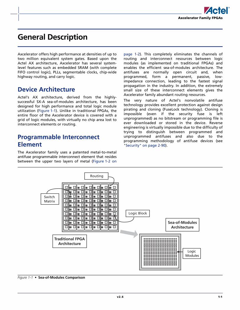
Device ArchitectureActel's AX architecture, derived from the highly-successful SX-A sea-of-modules architecture, has beendesigned for high performance and total logic moduleutilization (Figure 1-1). Unlike in traditional FPGAs, theentire floor of the Axcelerator device is covered with agrid of logic modules, with virtually no chip area lost tointerconnect elements or routing.
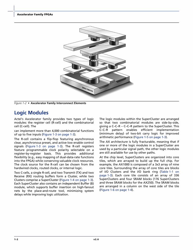
Programmable Interconnect ElementThe Axcelerator family uses a patented metal-to-metalantifuse programmable interconnect element that residesbetween the upper two layers of metal (Figure 1-2 on
page 1-2). This completely eliminates the channels ofrouting and interconnect resources between logicmodules (as implemented on traditional FPGAs) andenables the efficient sea-of-modules architecture. Theantifuses are normally open circuit and, whenprogrammed, form a permanent, passive, low-impedance connection, leading to the fastest signalpropagation in the industry. In addition, the extremelysmall size of these interconnect elements gives theAxcelerator family abundant routing resources.
The very nature of Actel's nonvolatile antifusetechnology provides excellent protection against designpirating and cloning (FuseLock technology). Cloning isimpossible (even if the security fuse is leftunprogrammed) as no bitstream or programming file isever downloaded or stored in the device. Reverseengineering is virtually impossible due to the difficulty oftrying to distinguish between programmed andunprogrammed antifuses and also due to theprogramming methodology of antifuse devices (see"Security" on page 2-90).
Figure 1-1 • Sea-of-Modules Comparison
Switch Matrix
Routing
Logic Block
Logic Modules
Sea-of-ModulesArchitecture
Traditional FPGAArchitecture
Axcelerator Family FPGAs
1-2 v2.6
Logic ModulesActel's Axcelerator family provides two types of logicmodules: the register cell (R-cell) and the combinatorialcell (C-cell). The
can implement more than 4,000 combinatorial functionsof up to five inputs (Figure 1-3 on page 1-3).
The R-cell contains a flip-flop featuring asynchronousclear, asynchronous preset, and active-low enable controlsignals (Figure 1-3 on page 1-3). The R-cell registersfeature programmable clock polarity selectable on aregister-by-register basis. This provides additionalflexibility (e.g., easy mapping of dual-data-rate functionsinto the FPGA) while conserving valuable clock resources.The clock source for the R-cell can be chosen from thehardwired clocks, routed clocks, or internal logic.
Two C-cells, a single R-cell, and two Transmit (TX) and twoReceive (RX) routing buffers form a Cluster, while twoClusters comprise a SuperCluster (Figure 1-4 on page 1-3).Each SuperCluster also contains an independent Buffer (B)module, which supports buffer insertion on high-fanoutnets by the place-and-route tool, minimizing systemdelays while improving logic utilization.
The logic modules within the SuperCluster are arrangedso that two combinatorial modules are side-by-side,giving a C–C–R – C–C–R pattern to the SuperCluster. ThisC–C–R pattern enables efficient implementation(minimum delay) of two-bit carry logic for improvedarithmetic performance (Figure 1-5 on page 1-3).
The AX architecture is fully fracturable, meaning that ifone or more of the logic modules in a SuperCluster areused by a particular signal path, the other logic modulesare still available for use by other paths.
At the chip level, SuperClusters are organized into coretiles, which are arrayed to build up the full chip. Forexample, the AX1000 is composed of a 3x3 array of ninecore tiles. Surrounding the array of core tiles are blocksof I/O Clusters and the I/O bank ring (Table 1-1 onpage 1-3). Each core tile consists of an array of 336SuperClusters and four SRAM blocks (176 SuperClustersand three SRAM blocks for the AX250). The SRAM blocksare arranged in a column on the west side of the tile(Figure 1-6 on page 1-4).
Figure 1-2 • Axcelerator Family Interconnect Elements

Axcelerator Family FPGAs
v2.6 1-3
Figure 1-3 • AX C-Cell and R-Cell
Figure 1-4 • AX SuperCluster
Figure 1-5 • AX 2-bit Carry Logic
Table 1-1 • Number of Core Tiles per Device
Device Number of Core Tiles
AX125 1 regular tile
AX250 4 smaller tiles
AX500 4 regular tiles
AX1000 9 regular tiles
AX2000 16 regular tiles
C-cell
A[1:0]B[1:0]
D[3:0]DB
CFN
FCO
FCI
Y
PSET
CLR
DE
CLK
Q
(Positive Edge Triggered)
C-Cell R-Cell
RX
TX
BC R CC C R
RX RX RX
TX TXTX
DCOUT
YY
C-Cell C-Cell
Carry Logic
FCI
FCO

Axcelerator Family FPGAs
1-4 v2.6
Embedded MemoryAs mentioned earlier, each core tile has either three (in asmaller tile) or four (in the regular tile) embedded SRAMblocks along the west side, and each variable-aspect-ratio SRAM block is 4,608 bits in size. Available memoryconfigurations are: 128x36, 256x18, 512x9, 1kx4, 2kx2 or4kx1 bits. The individual blocks have separate read andwrite ports that can be configured with different bitwidths on each port. For example, data can be written inby eight and read out by one.
In addition, every SRAM block has an embedded FIFOcontrol unit. The control unit allows the SRAM block tobe configured as a synchronous FIFO without using corelogic modules. The FIFO width and depth areprogrammable. The FIFO also features programmableALMOST-EMPTY (AEMPTY) and ALMOST-FULL (AFULL)flags in addition to the normal EMPTY and FULL flags. Inaddition to the flag logic, the embedded FIFO controlunit also contains the counters necessary for thegeneration of the read and write address pointers as well
as control circuitry to prevent metastability anderroneous operation. The embedded SRAM/FIFO blockscan be cascaded to create larger configurations.
I/O LogicThe Axcelerator family of FPGAs features a flexible I/Ostructure, supporting a range of mixed voltages with itsbank-selectable I/Os: 1.5V, 1.8V, 2.5V, and 3.3V. In all,Axcelerator FPGAs support at least 14 different I/Ostandards (single-ended, differential, voltage-referenced).The I/Os are organized into banks, with eight banks perdevice (two per side). The configuration of these banksdetermines the I/O standards supported (see "User I/Os"on page 2-10 for more information). All I/O standards areavailable in each bank.
Each I/O module has an input register (InReg), an outputregister (OutReg), and an enable register (EnReg)(Figure 1-7 on page 1-5). An I/O Cluster includes two I/Omodules, four RX modules, two TX modules, and a buffer(B) module.
Figure 1-6 • AX Device Architecture (AX1000 shown)
Chip Layout
SuperCluster
I/O Structure
See Figure 7
RAMC
RAMC
RAMC
RAMC
RAMC
RAMC
RAMC
RAMC
RAMC
RAMC
RAMC
RAMC
RAMC
RAMC
RAMC
RAMC
RAMC
RAMC
RAMC
RAMC
RAMC
RAMC
RAMC
RAMC
RAMC
RAMC
RAMC
RAMC
HD
SC
SC
SC
SC
SC
SC
SC
SC
SC
SC
SC
SC
SC
SC
SC
SC
SC
SC
SC
SC
SC
SC
SC
SC
HD
SC
SC
SC
SC
SC
SC
SC
SC
SC
SC
SC
SC
SC
SC
SC
SC
SC
SC
SC
SC
SC
SC
SC
SC
SC
SC
SC
SC
HD
SC
SC
SC
SC
SC
SC
SC
SC
SC
SC
SC
SC
SC
SC
SC
SC
SC
SC
SC
SC
SC
SC
SCSC
SC
SC
SC
SC
SC
HD
SC
SC
SC
SC
SC
SC
SC
SC
SC
SC
SC
SC
SC
SC
SC
SC
SC
SC
SC
SC
SC
SC
SC
SC
SC
SC
SC
SC
HD
SC
SC
SC
SC
SC
SC
SC
SC
SC
SC
SC
SC
SC
SC
SC
SC
SC
SC
SC
SC
SC
SC
SC
SC
SC
SC
SC
SC
HD
SC
SC
SC
SC
SC
SC
SC
SC
SC
SC
SC
SC
SC
SC
SC
SC
SC
SC
SC
SC
SC
SC
SC
SC
SC
SC
SC
SC
HD
SC
SC
SC
SC
RD
RD
RD
RD
RD
RD
RD
RD
RD
RD
RD
RD
RD
RD
RD
RD
RD
RD
RD
RD
RD
RD
RD
RD
RD
RD
RD
RD
SC
SC
SC
SC
SC
SC
SC
SC
SC
SC
SC
SC
SC
SC
SC
SC
SC
SC
SC
SC
SC
SC
SC
SC
HD
SC
SC
SC
SC
SC
SC
SC
SC
SC
SC
SC
SC
SC
SC
SC
SC
SC
SC
SC
SC
SC
SC
SC
SC
SC
SC
SC
SC
HD
SC
SC
SC
SC
SC
SC
SC
SC
SC
SC
SC
SC
SC
SC
SC
SC
SC
SC
SC
SC
SC
SC
SC
SC
SC
SC
SC
SC
HD
SC
SC
SC
SC
SC
SC
SC
SC
SC
SC
SC
SC
SC
SC
SC
SC
SC
SC
SC
SC
SC
SC
SC
SC
SC
SC
SC
SC
HD
SC
SC
SC
SC
SC
SC
SC
SC
SC
SC
SC
SC
SC
SC
SC
SC
SC
SC
SC
SC
SC
SC
SC
SC
SC
SC
SC
SC
HD
SC
SC
SC
SC
SC
SC
SC
SC
SC
SC
SC
SC
SC
SC
SC
SC
SC
SC
SC
SC
SC
SC
SC
SC
SC
SC
SC
SC
HD
SC
SC
SC
SC
Core Tile
4k RAM/ FIFO
4k RAM/ FIFO
4k RAM/ FIFO
4k RAM/ FIFO
RX
TX
BC R CC C R
RX RX RX
TX TXTX

Axcelerator Family FPGAs
v2.6 1-5
RoutingThe AX hierarchical routing structure ties the logicmodules, the embedded memory blocks, and the I/Omodules together (Figure 1-8 on page 1-6). At the lowestlevel, in and between SuperClusters, there are three localrouting structures: FastConnect, DirectConnect, andCarryConnect routing. DirectConnects provide the highestperformance routing inside the SuperClusters byconnecting a C-cell to the adjacent R-cell. DirectConnectsdo not require an antifuse to make the connection andachieve a signal propagation time of less than 0.1 ns.
FastConnects provide high-performance, horizontalrouting inside the SuperCluster and vertical routing tothe SuperCluster immediately below it. Only oneprogrammable connection is used in a FastConnect path,delivering a maximum routing delay of 0.4 ns.
CarryConnects are used for routing carry logic betweenadjacent SuperClusters. They connect the FCO output ofone two-bit, C-cell carry logic to the FCI input of the two-bit, C-cell carry logic of the SuperCluster below it.CarryConnects do not require an antifuse to make theconnection and achieve a signal propagation time of lessthan 0.1 ns.
The next level contains the core tile routing. Over theSuperClusters within a core tile, both vertical andhorizontal tracks run across rows or columns,respectively. At the chip level, vertical and horizontaltracks extend across the full length of the device, bothnorth-to-south and east-to-west. These tracks arecomposed of highway routing that extend the entirelength of the device (segmented at core tile boundaries)as well as segmented routing of varying lengths.
Global ResourcesEach family member has three types of global signalsavailable to the designer: HCLK, CLK, and GCLR/GPSET.There are four hardwired clocks (HCLK) per device thatcan directly drive the clock input of each R-cell. Each ofthe four routed clocks (CLK) can drive the clock, clear,preset, or enable pin of an R-cell or any input of a C-cell(Figure 1-3 on page 1-3).
Global clear (GCLR) and global preset (GPSET) drive theclear and preset inputs of each R-cell as well as each I/ORegister on a chip-wide basis at power-up.
Each HCLK and CLK has an associated analog PLL (a totalof eight per chip). Each embedded PLL can be used forclock delay minimization, clock delay adjustment, orclock frequency synthesis. The PLL is capable of
Figure 1-7 • I/O Cluster Arrangement
I/O Cluster
I/O Module
CoreTile
4kRAM/FIFO
4kRAM/FIFO
4kRAM/FIFO
4kRAM/FIFO
OutReg EnRegInReg
I/O Module
I/O Module
RX RX RX RX
TX TX
BN
I
O
BA
K

Axcelerator Family FPGAs
1-6 v2.6
operating with input frequencies ranging from 14 MHzto 200 MHz and can generate output frequenciesbetween 20 MHz and 1 GHz. The clock can be eitherdivided or multiplied by factors ranging from 1 to 64.Additionally, multiply and divide settings can be used inany combination as long as the resulting clock frequencyis between 20 MHz and 1 GHz. Adjacent PLLs can becascaded to create complex frequency combinations.
The PLL can be used to introduce either a positive or anegative clock delay of up to 3.75 ns in 250 psincrements. The reference clock required to drive the PLLcan be derived from three sources: external input pad(either single-ended or differential), internal logic, or theoutput of an adjacent PLL.
Low Power (LP) ModeThe AX architecture was created for high-performancedesigns but also includes a low power mode (activated viathe LP pin). When the low power mode is activated, I/Obanks can be disabled (inputs disabled, outputs tristated),and PLLs can be placed in a power-down mode. Allinternal register states are maintained in this mode.Furthermore, individual I/O banks can be configured toopt out of the LP mode, thereby giving the designer accessto critical signals while the rest of the chip is in low powermode.
The power can be further reduced by providing anexternal voltage source (VPUMP) to the device to bypassthe internal charge pump (See "Low Power Mode" onpage 2-89 for more information).
Design EnvironmentThe Axcelerator family of FPGAs is fully supported by bothActel's Libero™ Integrated Design Environment andDesigner FPGA Development software. Actel Libero IDE isan integrated design manager that seamlessly integratesdesign tools while guiding the user through the designflow, managing all design and log files, and passingnecessary design data among tools. Additionally, LiberoIDE allows users to integrate both schematic and HDLsynthesis into a single flow and verify the entire design ina single environment (see the Libero IDE Flow diagramlocated on Actel’s website). Libero IDE includes Synplify®
Actel Edition (AE) from Synplicity®, ViewDraw® AE fromMentor Graphics®, ModelSim® HDL Simulator fromMentor Graphics, WaveFormer Lite™ AE fromSynaptiCAD®, and Designer software from Actel.
Actel's Designer software is a place-and-route tool andprovides a comprehensive suite of backend support toolsfor FPGA development. The Designer software includesthe following:
• Timer – a world-class integrated static timing analyzerand constraints editor which support timing-drivenplace-and-route
• NetlistViewer – a design netlist schematic viewer• ChipPlanner – a graphical floorplanner viewer and editor• SmartPower – allows the designer to quickly estimate
the power consumption of a design• PinEditor – a graphical application for editing pin
assignments and I/O attributes• I/O Attribute Editor – displays all assigned and
unassigned I/O macros and their attributes in aspreadsheet format
Figure 1-8 • AX Routing Structures

Axcelerator Family FPGAs
v2.6 1-7
With the Designer software, a user can lock the designpins before layout while minimally impacting the resultsof place-and-route. Additionally, Actel’s back-annotationflow is compatible with all the major simulators and thesimulation results can be cross-probed with SiliconExplorer II, Actel’s integrated verification and logicanalysis tool. Another tool included in the Designersoftware is the ACTgen macro builder, which easilycreates popular and commonly used logic functions forimplementation into your schematic or HDL design.
Actel's Designer software is compatible with the mostpopular FPGA design entry and verification tools fromEDA vendors, such as Mentor Graphics, Synplicity,Synopsys, and Cadence Design Systems. The Designersoftware is available for both the Windows and UNIXoperating systems.
ProgrammingProgramming support is provided through Actel's SiliconSculptor II, a single-site programmer driven via a PC-based GUI. In addition, BP Microsystems offers multi-siteprogrammers that provide qualified support for Acteldevices. Factory programming is available for high-volume production needs.
In-System Diagnostic and Debug CapabilitiesThe Axcelerator family of FPGAs includes internal probecircuitry, allowing the designer to dynamically observeand analyze any signal inside the FPGA without disturbingnormal device operation. Up to four individual signals canbe brought out to dedicated probe pins (PRA/B/C/D) onthe device. The probe circuitry is accessed and controlledvia Silicon Explorer II (Figure 1-9), Actel's integratedverification and logic analysis tool that attaches to theserial port of a PC and communicates with the FPGA viathe JTAG port (See "Silicon Explorer II Probe Interface"on page 2-91).
SummaryActel’s Axcelerator family of FPGAs extends thesuccessful SX-A architecture, adding embedded RAM/FIFOs, PLLs, and high-speed I/Os. With the support of asuite of robust software tools, design engineers canincorporate high gate counts and fixed pins into anAxcelerator design yet still achieve high performanceand efficient device utilization.
Figure 1-9 • Probe Setup
SerialConnection
Additional 14 Channels(Logic Analyzer)
Axcelerator FPGAs
Silicon Explorer II
TDI
TCK
TMS
16 PinConnection
22 PinConnection
PRA
PRB
TDO
CH3/PRCCH4/PRD

Axcelerator Family FPGAs
1-8 v2.6
Related Documents
Application NotesSimultaneous Switching Noise and Signal Integrity
http://www.actel.com/documents/SSN_AN.pdf
Axcelerator Family PLL and Clock Management
http://www.actel.com/documents/AX_PLL_AN.pdf
Implementing DDR Transmit in Axcelerator
http://www.actel.com/documents/AX_DDR_AN.pdf
Implementation of Security in Actel Antifuse FPGAs
http://www.actel.com/documents/Antifuse_Security_AN.pdf
User’s Guides and ManualsAntifuse Macro Library Guide
http://www.actel.com/documents/libguide_UG.pdf
ACTgen Macros User’s Guide
http://www.actel.com/documents/genguide_UG.pdf
Silicon Sculptor II User’s Guide
http://www.actel.com/techdocs/manuals/default.asp
White PaperDesign Security in Nonvolatile Flash and Antifuse FPGAs
http://www.actel.com/documents/DesignSecurity_WP.pdf
Understanding Actel Antifuse Device Security
http://www.actel.com/documents/AntifuseSecurity_WP.pdf
MiscellaneousLibero IDE flow diagram
http://www.actel.com/products/tools/libero/flow.html

Axcelerator Family FPGAs
v2.6 2-1
Detailed Specifications
Operating ConditionsTable 2-1 lists the absolute maximum ratings of Axcelerator devices. Stresses beyond the ratings may cause permanentdamage to the device. Exposure to Absolute Maximum rated conditions for extended periods may affect devicereliability. Devices should not be operated outside the recommendations in Table 2-2.
Power-Up/Down SequenceAll Axcelerator I/Os are tristated during power-up until normal device operating conditions are reached, when I/Osenter user mode. VCCDA should be powered up before (or coincidentally with) VCCA and VCCI to ensure the behavior ofuser I/Os at system start-up. Conversely, VCCDA should be powered down after (or coincidentally with) VCCA and VCCI.Note that VCCI and VCCA can be powered up in any sequence with respect to each other, provided the requirementwith respect to VCCDA is satisfied.
Table 2-1 • Absolute Maximum Ratings
Symbol Parameter Limits Units
VCCA DC Core Supply Voltage –0.3 to 1.6 V
VCCI DC I/O Supply Voltage –0.3 to 3.75 V
VREF DC I/O Reference Voltage –0.3 to 3.75 V
VI Input Voltage –0.5 to 3.75 V
VO Output Voltage –0.5 to 3.75 V
TSTG Storage Temperature –60 to +150 °C
VCCDA* Supply Voltage for Differential I/Os –0.3 to 3.75 V
Note: * Should be the maximum of all VCCI.
Table 2-2 • Recommended Operating Conditions
Parameter Range Commercial Industrial Military Units
Ambient Temperature (TA)1 0 to +70 –40 to +85 –55 to +125 °C
1.5V Core Supply Voltage 1.425 to 1.575 1.425 to 1.575 1.425 to 1.575 V
1.5V I/O Supply Voltage 1.425 to 1.575 1.425 to 1.575 1.425 to 1.575 V
1.8V I/O Supply Voltage 1.71 to 1.89 1.71 to 1.89 1.71 to 1.89 V
2.5V I/O Supply Voltage 2.375 to 2.625 2.375 to 2.625 2.375 to 2.625 V
3.3V I/O Supply Voltage 3.0 to 3.6 3.0 to 3.6 3.0 to 3.6 V
VCCDA Supply Voltage 3.0 to 3.6 3.0 to 3.6 3.0 to 3.6 V
VPUMP Supply Voltage 3.0 to 3.6 3.0 to 3.6 3.0 to 3.6 V
Notes:
1. Ambient temperature (TA) is used for commercial and industrial grades; case temperature (TC) is used for military grades.2. TJ max = 125°C
Axcelerator Family FPGAs
2-2 v2.6
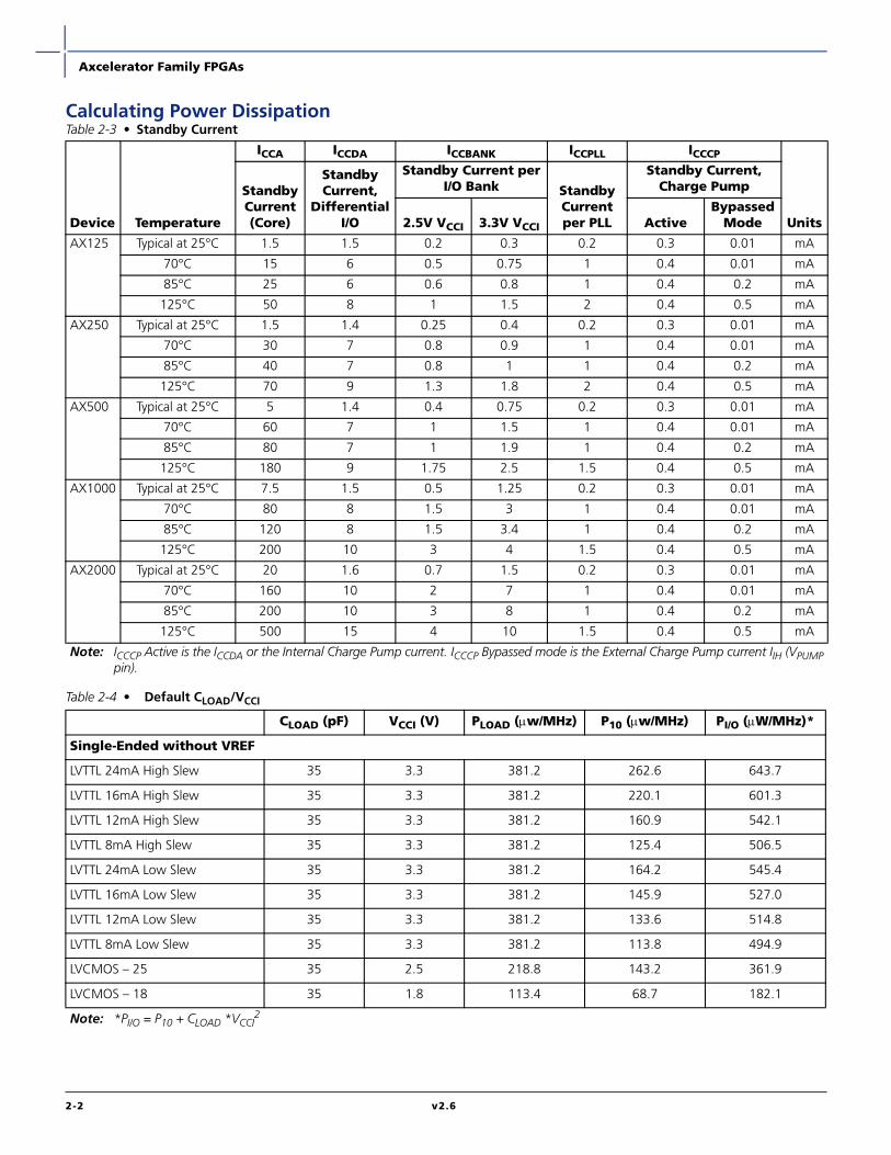
Calculating Power Dissipation Table 2-3 • Standby Current
Device Temperature
ICCA ICCDA ICCBANK ICCPLL ICCCP
Units
Standby Current (Core)
Standby Current,
Differential I/O
Standby Current perI/O Bank Standby
Current per PLL
Standby Current,Charge Pump
2.5V VCCI 3.3V VCCI ActiveBypassed
Mode
AX125 Typical at 25°C 1.5 1.5 0.2 0.3 0.2 0.3 0.01 mA
70°C 15 6 0.5 0.75 1 0.4 0.01 mA
85°C 25 6 0.6 0.8 1 0.4 0.2 mA
125°C 50 8 1 1.5 2 0.4 0.5 mA
AX250 Typical at 25°C 1.5 1.4 0.25 0.4 0.2 0.3 0.01 mA
70°C 30 7 0.8 0.9 1 0.4 0.01 mA
85°C 40 7 0.8 1 1 0.4 0.2 mA
125°C 70 9 1.3 1.8 2 0.4 0.5 mA
AX500 Typical at 25°C 5 1.4 0.4 0.75 0.2 0.3 0.01 mA
70°C 60 7 1 1.5 1 0.4 0.01 mA
85°C 80 7 1 1.9 1 0.4 0.2 mA
125°C 180 9 1.75 2.5 1.5 0.4 0.5 mA
AX1000 Typical at 25°C 7.5 1.5 0.5 1.25 0.2 0.3 0.01 mA
70°C 80 8 1.5 3 1 0.4 0.01 mA
85°C 120 8 1.5 3.4 1 0.4 0.2 mA
125°C 200 10 3 4 1.5 0.4 0.5 mA
AX2000 Typical at 25°C 20 1.6 0.7 1.5 0.2 0.3 0.01 mA
70°C 160 10 2 7 1 0.4 0.01 mA
85°C 200 10 3 8 1 0.4 0.2 mA
125°C 500 15 4 10 1.5 0.4 0.5 mA
Note: ICCCP Active is the ICCDA or the Internal Charge Pump current. ICCCP Bypassed mode is the External Charge Pump current IIH (VPUMPpin).
Table 2-4 • Default CLOAD/VCCI
CLOAD (pF) VCCI (V) PLOAD (µw/MHz) P10 (µw/MHz) PI/O (µW/MHz)*
Single-Ended without VREF
LVTTL 24mA High Slew 35 3.3 381.2 262.6 643.7
LVTTL 16mA High Slew 35 3.3 381.2 220.1 601.3
LVTTL 12mA High Slew 35 3.3 381.2 160.9 542.1
LVTTL 8mA High Slew 35 3.3 381.2 125.4 506.5
LVTTL 24mA Low Slew 35 3.3 381.2 164.2 545.4
LVTTL 16mA Low Slew 35 3.3 381.2 145.9 527.0
LVTTL 12mA Low Slew 35 3.3 381.2 133.6 514.8
LVTTL 8mA Low Slew 35 3.3 381.2 113.8 494.9
LVCMOS – 25 35 2.5 218.8 143.2 361.9
LVCMOS – 18 35 1.8 113.4 68.7 182.1
Note: *PI/O = P10 + CLOAD *VCCI2

Axcelerator Family FPGAs
v2.6 2-3
LVCMOS - 15 (JESD8-11) 35 1.5 78.8 44.9 123.6
PCI 10 3.3 108.9 213.5 322.4
PCI-X 10 3.3 108.9 158.0 266.9
Single-Ended with VREF
HSTL-I 20 1.5 - 36.8 36.8
SSTL2-I 30 2.5 - 166.9 166.9
SSTL2-II 30 2.5 - 143.5 143.5
SSTL3-I 30 3.3 - 322.8 322.8
SSTL3-II 30 3.3 - 284.0 284.0
GTLP - 25 10 2.5 - TBD TBD
GTLP - 33 10 3.3 - TBD TBD
Differential
LVPECL - 33 N/A 3.3 - 255.1 255.1
LVDS - 25 N/A 2.5 - 140.4 140.4
Table 2-5 • Different Components Contributing to the Total Power Consumption in Axcelerator Devices
Component Definition
Device Specific Value (in µW/MHz)
AX125 AX250 AX500 AX1000 AX2000
P1 Core tile HCLK power component 33 49 71 130 216
P2 R-cell power component 0.2 0.2 0.2 0.2 0.2
P3 HCLK signal power dissipation 4.5 4.5 9 13.5 18
P4 Core tile RCLK power component 33 49 71 130 216
P5 R-cell power component 0.3 0.3 0.3 0.3 0.3
P6 RCLK signal power dissipation 6.5 6.5 13 19.5 26
P7 Power dissipation due to the switching activity on the R-cell 1.6 1.6 1.6 1.6 1.6
P8 Power dissipation due to the switching activity on the C-cell 1.4 1.4 1.4 1.4 1.4
P9 Power component associated with the input voltage 10 10 10 10 10
P10 Power component associated with the output voltage See table Per pin contribution
P11 Power component associated with the read operation in the RAMblock
25 25 25 25 25
P12 Power component associated with the write operation in the RAMblock
30 30 30 30 30
P13 Core PLL power component 1.5 1.5 1.5 1.5 1.5
Table 2-4 • Default CLOAD/VCCI (Continued)
CLOAD (pF) VCCI (V) PLOAD (µw/MHz) P10 (µw/MHz) PI/O (µW/MHz)*
Note: *PI/O = P10 + CLOAD *VCCI2
Axcelerator Family FPGAs
2-4 v2.6
Ptotal = Pdc + Pac
PHCLK = (P1 + P2 * s + P3 * sqrt[s]) * Fs
PCLK = (P4 + P5 * s + P6 * sqrt[s]) * Fs
PR-cells = P7 * ms * Fs
PC-cells = P8 * mc * Fs
Pinputs = P9 * pi * Fpi
Poutputs = PI/O * po * Fpo
Pmemory = P11 * Nblock * FRCLK + P12 * Nblock * FWCLK
PPLL = P13 * FCLK
Pdc = ICCA * VCCA
Pac = PHCLK + PCLK + PR-cells + PC-cells + Pinputs + Poutputs + Pmemory + PPLL
s = the number of R-cells clocked by this clock
Fs = the clock frequency
s = the number of R-cells clocked by this clock
Fs = the clock frequency
ms = the number of R-cells switching at each Fs cycle
Fs = the clock frequency
mc = the number of C-cells switching at each Fs cycle
Fs = the clock frequency
pi = the number of inputs
Fpi = the average input frequency
Cload = the output load (technology dependent)
VCCI = the output voltage (technology dependent)
po = the number of outputs
Fpo = the average output frequency
Nblock = the number of RAM/FIFO blocks (1 block = 4k)
FRCLK = the read-clock frequency of the memory
FWCLK = the write-clock frequency of the memory
FRefCLK = the clock frequency of the clock input of the PLL
FCLK = the clock frequency of the first clock output of the PLL
Axcelerator Family FPGAs
v2.6 2-5
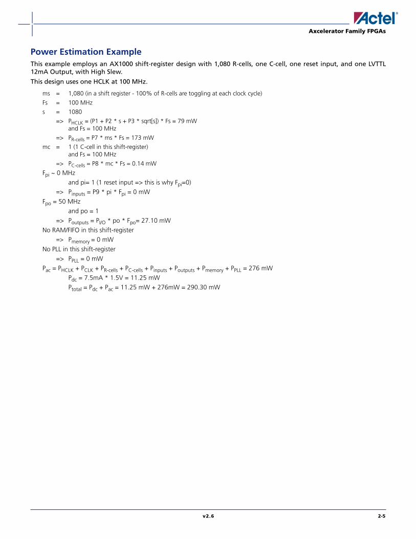
Power Estimation Example This example employs an AX1000 shift-register design with 1,080 R-cells, one C-cell, one reset input, and one LVTTL12mA Output, with High Slew.
This design uses one HCLK at 100 MHz.
ms = 1,080 (in a shift register - 100% of R-cells are toggling at each clock cycle)
Fs = 100 MHz
s = 1080
=> PHCLK = (P1 + P2 * s + P3 * sqrt[s]) * Fs = 79 mWand Fs = 100 MHz
=> PR-cells = P7 * ms * Fs = 173 mW
mc = 1 (1 C-cell in this shift-register)and Fs = 100 MHz
=> PC-cells = P8 * mc * Fs = 0.14 mW
Fpi ~ 0 MHz
and pi= 1 (1 reset input => this is why Fpi=0)=> Pinputs = P9 * pi * Fpi = 0 mW
Fpo = 50 MHz
and po = 1
=> Poutputs = PI/O * po * Fpo= 27.10 mW
No RAM/FIFO in this shift-register=> Pmemory = 0 mW
No PLL in this shift-register
=> PPLL = 0 mW
Pac = PHCLK + PCLK + PR-cells + PC-cells + Pinputs + Poutputs + Pmemory + PPLL = 276 mW
Pdc = 7.5mA * 1.5V = 11.25 mW
Ptotal = Pdc + Pac = 11.25 mW + 276mW = 290.30 mW
Axcelerator Family FPGAs
2-6 v2.6
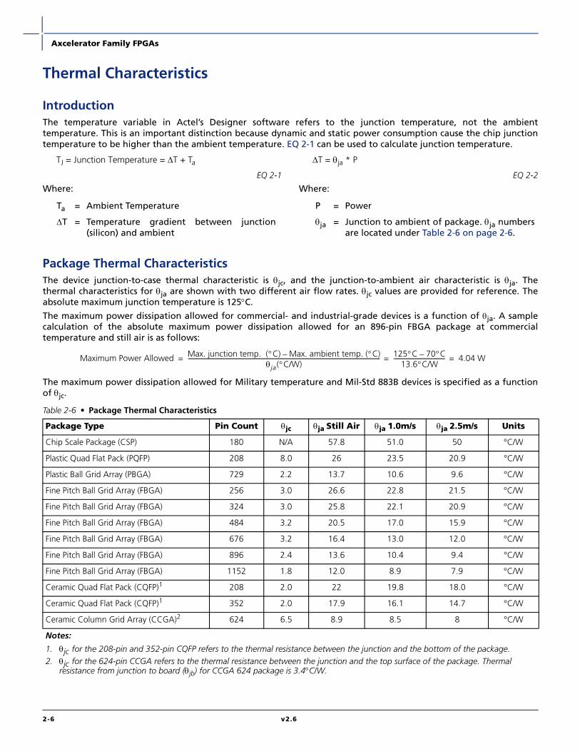
Thermal Characteristics
IntroductionThe temperature variable in Actel’s Designer software refers to the junction temperature, not the ambienttemperature. This is an important distinction because dynamic and static power consumption cause the chip junctiontemperature to be higher than the ambient temperature. EQ 2-1 can be used to calculate junction temperature.
TJ = Junction Temperature = ∆T + Ta
EQ 2-1
Where:
∆T = θja * P
EQ 2-2
Where:
Package Thermal CharacteristicsThe device junction-to-case thermal characteristic is θjc, and the junction-to-ambient air characteristic is θja. Thethermal characteristics for θja are shown with two different air flow rates. θjc values are provided for reference. Theabsolute maximum junction temperature is 125°C.
The maximum power dissipation allowed for commercial- and industrial-grade devices is a function of θja. A samplecalculation of the absolute maximum power dissipation allowed for an 896-pin FBGA package at commercialtemperature and still air is as follows:
The maximum power dissipation allowed for Military temperature and Mil-Std 883B devices is specified as a functionof θjc.
Ta = Ambient Temperature
∆T = Temperature gradient between junction(silicon) and ambient
P = Power
θja = Junction to ambient of package. θja numbersare located under Table 2-6 on page 2-6.
Table 2-6 • Package Thermal Characteristics
Package Type Pin Count θjc θja Still Air θja 1.0m/s θja 2.5m/s Units
Chip Scale Package (CSP) 180 N/A 57.8 51.0 50 °C/W
Plastic Quad Flat Pack (PQFP) 208 8.0 26 23.5 20.9 °C/W
Plastic Ball Grid Array (PBGA) 729 2.2 13.7 10.6 9.6 °C/W
Fine Pitch Ball Grid Array (FBGA) 256 3.0 26.6 22.8 21.5 °C/W
Fine Pitch Ball Grid Array (FBGA) 324 3.0 25.8 22.1 20.9 °C/W
Fine Pitch Ball Grid Array (FBGA) 484 3.2 20.5 17.0 15.9 °C/W
Fine Pitch Ball Grid Array (FBGA) 676 3.2 16.4 13.0 12.0 °C/W
Fine Pitch Ball Grid Array (FBGA) 896 2.4 13.6 10.4 9.4 °C/W
Fine Pitch Ball Grid Array (FBGA) 1152 1.8 12.0 8.9 7.9 °C/W
Ceramic Quad Flat Pack (CQFP)1 208 2.0 22 19.8 18.0 °C/W
Ceramic Quad Flat Pack (CQFP)1 352 2.0 17.9 16.1 14.7 °C/W
Ceramic Column Grid Array (CCGA)2 624 6.5 8.9 8.5 8 °C/W
Notes:
1. θjc for the 208-pin and 352-pin CQFP refers to the thermal resistance between the junction and the bottom of the package.2. θjc for the 624-pin CCGA refers to the thermal resistance between the junction and the top surface of the package. Thermal
resistance from junction to board (θjb) for CCGA 624 package is 3.4°C/W.
Maximum Power Allowed Max. junction temp. (°C) Max. ambient temp. (°C)–θja(°C/W)
--------------------------------------------------------------------------------------------------------------------------------------- 125°C 70°C–13.6°C/W
------------------------------------ 4.04 W===
Axcelerator Family FPGAs
v2.6 2-7
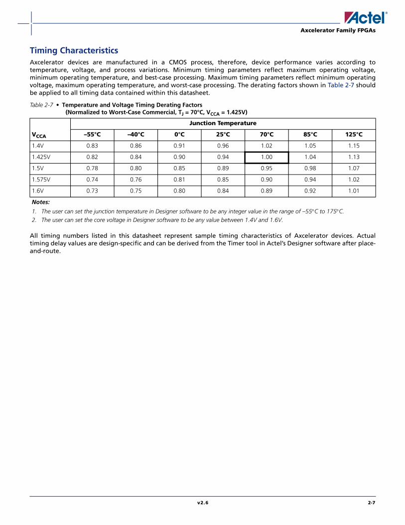
Timing CharacteristicsAxcelerator devices are manufactured in a CMOS process, therefore, device performance varies according totemperature, voltage, and process variations. Minimum timing parameters reflect maximum operating voltage,minimum operating temperature, and best-case processing. Maximum timing parameters reflect minimum operatingvoltage, maximum operating temperature, and worst-case processing. The derating factors shown in Table 2-7 shouldbe applied to all timing data contained within this datasheet.
All timing numbers listed in this datasheet represent sample timing characteristics of Axcelerator devices. Actualtiming delay values are design-specific and can be derived from the Timer tool in Actel’s Designer software after place-and-route.
Table 2-7 • Temperature and Voltage Timing Derating Factors(Normalized to Worst-Case Commercial, TJ = 70°C, VCCA = 1.425V)
VCCA
Junction Temperature
–55°C –40°C 0°C 25°C 70°C 85°C 125°C
1.4V 0.83 0.86 0.91 0.96 1.02 1.05 1.15
1.425V 0.82 0.84 0.90 0.94 1.00 1.04 1.13
1.5V 0.78 0.80 0.85 0.89 0.95 0.98 1.07
1.575V 0.74 0.76 0.81 0.85 0.90 0.94 1.02
1.6V 0.73 0.75 0.80 0.84 0.89 0.92 1.01
Notes:
1. The user can set the junction temperature in Designer software to be any integer value in the range of –55°C to 175°C.2. The user can set the core voltage in Designer software to be any value between 1.4V and 1.6V.

Axcelerator Family FPGAs
2-8 v2.6
Timing Model
Hardwired Clock – Using LVTTL 24mA High Slew Clock I/O
Routed Clock – Using LVTTL 24mA High Slew Clock I/O
Note: Worst case timing data for the AX1000, –2 speed gradeFigure 2-1 • Worst Case Timing Data
CombinatorialCell
CombinatorialCell
CombinatorialCell
CombinatorialCell
D Q D Q D Q
Y
FCO
+
+
Routed Clock
Register Cell
LVPECL
LVPECL
LVDS
Register Cell
Hardwired orRouted Clock
Hardwired Clock
I/O Module
I/O Module (Registered) I/O Module
(Nonregistered)
I/O Module (Non- registered)
I/O Module (Nonregistered)
Y
Buffer Module
Buffer Module
Buffer Module
Carry Chain
I/O
I/O
LVTTL Output DriveStrength = 4 (24mA) High Slew Rate
tHCKH = 3.03 nsFMAX (external) = 350 MHz
FMAX (internal) = 870 MHz
tSUD = 0.23 nstICKLQ = 0.67 ns
tDP = 1.70 nstRD2 = 0.53 ns
tDP = 1.84 ns
tHCKL = 3.02 ns
tRCKL = 3.08 ns
tRCO = 0.67 nstSUD = 0.23 ns
tRD1 = 0.45 ns
tPD = 0.74 ns
tRCKL = 3.08 nsFMAX (external) = 350 MHzFMAX (internal) = 870 MHz
tRCO = 0.67 nstSUD = 0.23 ns
tBPFD = 0.12 ns
tPY = 1.01 nsGTL + 3.3V
tOCLKY = 0.67 ns tSUD = 0.23 ns
tBFPD = 0.12 ns tPD = 0.74 ns tBFPD = 0.12 ns
tPDC = 0.57 ns tCCY = 0.61 ns
tPY = 3.03 ns
tPY = 2.28 ns
tRD1 = 0.45 nstRD2 = 0.53 ns tRD3 = 0.56 ns
External Setup
= (tDP + tRD2 + tSUD) – tHCKL
= (1.72 + 0.53 + 0.23) – 3.02 = –0.54 ns
Clock-to-Out (Pad-to-Pad)
= tHCKL + tRCO + tRD1 + tPYs
= 3.02 + 0.67 + 0.45 + 3.03 = 7.17 ns
External Setup
= (tDP + tRD2 + tSUD) – tRCKH
= (1.72 + 0.53 + 0.23) – 3.13 = –0.65 ns
Clock-to-Out (Pad-to-Pad)
= tRCKH + tRCO + tRD1 + tPY
= 3.13 + 0.67 + 0.45 + 3.03 = 7.28 ns
Axcelerator Family FPGAs
v2.6 2-9
I/O Specifications
Pin Descriptions
Supply PinsGND Ground
Low supply voltage.
VCCA Supply Voltage
Supply voltage for array (1.5V). See "OperatingConditions" on page 2-1 for more information.
VCCIBx Supply Voltage
Supply voltage for I/Os. Bx is the I/O Bank ID – 0 to 7. See"Operating Conditions" on page 2-1 for moreinformation.
VCCDA Supply Voltage
Supply voltage for the I/O differential amplifier and JTAGand probe interfaces. See "Operating Conditions" onpage 2-1 for more information. VCCDA should be tied to3.3V.
VCCPLA/B/C/D/E/F/G/H Supply Voltage
PLL analog power supply (1.5V) for internal PLL. Thereare eight in each device. VCCPLA supports the PLLassociated with global resource HCLKA, VCCPLB supportsthe PLL associated with global resource HCLKB, etc. ThePLL analog power supply pins should be connected to1.5V whether PLL is used or not.
VCOMPLA/B/C/D/E/F/G/HSupply Voltage
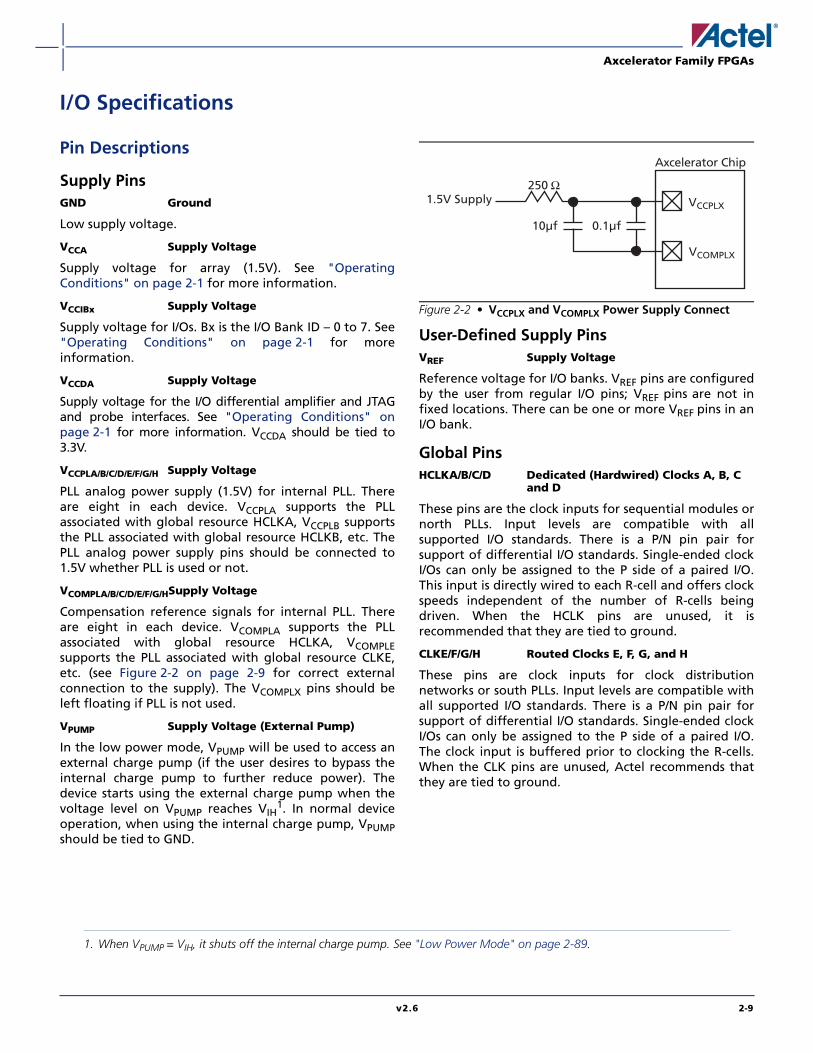
Compensation reference signals for internal PLL. Thereare eight in each device. VCOMPLA supports the PLLassociated with global resource HCLKA, VCOMPLEsupports the PLL associated with global resource CLKE,etc. (see Figure 2-2 on page 2-9 for correct externalconnection to the supply). The VCOMPLX pins should beleft floating if PLL is not used.
VPUMP Supply Voltage (External Pump)
In the low power mode, VPUMP will be used to access anexternal charge pump (if the user desires to bypass theinternal charge pump to further reduce power). Thedevice starts using the external charge pump when thevoltage level on VPUMP reaches VIH
1. In normal deviceoperation, when using the internal charge pump, VPUMPshould be tied to GND.
User-Defined Supply PinsVREF Supply Voltage
Reference voltage for I/O banks. VREF pins are configuredby the user from regular I/O pins; VREF pins are not infixed locations. There can be one or more VREF pins in anI/O bank.
Global PinsHCLKA/B/C/D Dedicated (Hardwired) Clocks A, B, C
and D
These pins are the clock inputs for sequential modules ornorth PLLs. Input levels are compatible with allsupported I/O standards. There is a P/N pin pair forsupport of differential I/O standards. Single-ended clockI/Os can only be assigned to the P side of a paired I/O.This input is directly wired to each R-cell and offers clockspeeds independent of the number of R-cells beingdriven. When the HCLK pins are unused, it isrecommended that they are tied to ground.
CLKE/F/G/H Routed Clocks E, F, G, and H
These pins are clock inputs for clock distributionnetworks or south PLLs. Input levels are compatible withall supported I/O standards. There is a P/N pin pair forsupport of differential I/O standards. Single-ended clockI/Os can only be assigned to the P side of a paired I/O.The clock input is buffered prior to clocking the R-cells.When the CLK pins are unused, Actel recommends thatthey are tied to ground.
1. When VPUMP = VIH, it shuts off the internal charge pump. See "Low Power Mode" on page 2-89.
Figure 2-2 • VCCPLX and VCOMPLX Power Supply Connect
1.5V Supply
Axcelerator Chip
0.1µf10µf
250 ΩVCCPLX
VCOMPLX
Axcelerator Family FPGAs
2-10 v2.6
JTAG/Probe PinsPRA/B/C/D Probe A/B/C/D
The Probe pins are used to output data from any user-defined design node within the device (controlled withSilicon Explorer II). These independent diagnostic pinscan be used to allow real-time diagnostic output of anysignal path within the device. The pins’ probecapabilities can be permanently disabled to protectprogrammed design confidentiality. The probe pins areof LVTTL output levels.
TCK Test Clock
Test clock input for JTAG boundary-scan testing anddiagnostic probe (Silicon Explorer II).
TDI Test Data Input
Serial input for JTAG boundary-scan testing anddiagnostic probe. TDI is equipped with an internal 10 kΩpull-up resistor.
TDO Test Data Output
Serial output for JTAG boundary-scan testing.
TMS Test Mode Select
The TMS pin controls the use of the IEEE 1149.1boundary-scan pins (TCK, TDI, TDO, TRST). TMS isequipped with an internal 10 kΩ pull-up resistor.
TRST Boundary Scan Reset Pin
The TRST pin functions as an active-low input toasynchronously initialize or reset the boundary scan circuit.The TRST pin is equipped with a 10 kΩ pull-up resistor.
Special FunctionsLP Low Power Pin
The LP pin controls the low power mode of Axceleratordevices. The device is placed in the low power mode byconnecting the LP pin to logic high. To exit the lowpower mode, the LP pin must be set Low. Additionally,the LP pin must be set Low during chip powering-up orchip powering-down operations. See "Low PowerMode" on page 2-89 for more details.
NC No Connection
This pin is not connected to circuitry within the device.These pins can be driven to any voltage or can be leftfloating with no effect on the operation of the device.
User I/Os2
IntroductionThe Axcelerator family features a flexible I/O structure,supporting a range of mixed voltages (1.5V, 1.8V, 2.5V,and 3.3V) with its bank-selectable I/Os. Table 2-8 onpage 2-11 contains the I/O standards supported by theAxcelerator family, and Table 2-10 on page 2-11compares the features of the different I/O standards.Each I/O provides programmable slew rates, drivestrengths, and weak pull-up and weak pull-down circuits.I/O standards, except 3.3V PCI and 3.3V PCI-X, arecapable of hot insertion. 3.3V PCI and 3.3V PCI-X are 5Vtolerant with the aid of an external resistor. The input buffer has an optional user-configurable delayelement. The element can reduce or eliminate the holdtime requirement for input signals registered within theI/O cell. The value for the delay is set on a bank-widebasis. Note that the delay WILL be a function of processvariations as well as temperature and voltage changes.Each I/O includes three registers: an input (InReg), anoutput (OutReg), and an enable register (EnReg). I/Os areorganized into banks, and there are eight banks perdevice — two per side (Figure 2-6 on page 2-15). Each I/Obank has a common VCCI, the supply voltage for its I/Os. For voltage-referenced I/Os, each bank also has acommon reference-voltage bus, VREF. While VREF musthave a common voltage for an entire I/O bank, itslocation is user-selectable. In other words, any user I/O inthe bank can be selected to be a VREF. The location of the VREF pin should be selected accordingto the following rules:
• Any pin that is assigned as a VREF can control amaximum of eight user I/O pad locations in eachdirection (16 total maximum) within the same I/Obank.
• I/O pad locations listed as no connects are countedas part of the 16 maximum. In many cases, thisleads to fewer than eight user I/O package pins ineach direction being controlled by a VREF pin.
• Dedicated I/O pins (GND, VCCI...) are counted aspart of the 16.
• The two user I/O pads immediately adjacent on eachside of the VREF pin (four in total) may only be usedas an input. The exception is when there is a VCCI/GND pair separating the VREF pin and the user I/Opad location.
2. Do not use an external resister to pull the I/O above VCCI for a higher logic “1” voltage level. The desired higher logic “1”voltage level will be degraded due to a small I/O current, which exists when the I/O is pulled up above VCCI.

Axcelerator Family FPGAs
v2.6 2-11
The differential amplifier supply voltage VCCDA should beconnected to 3.3V. A user can gain access to the various I/O standards inthree ways:
• Instantiate specific library macros that representthe desired specific standard
• Use generic I/O macros and then use ActelDesigner’s PinEditor to specify the desired I/Ostandards (please note that this is not applicableto differential standards)
• A combination of the first two methods.Please refer to the I/O Features in Axcelerator FamilyDevices application note and the Antifuse Macro LibraryGuide for more details.
Table 2-8 • I/O Standards Supported by the Axcelerator Family
I/O StandardInput/Output Supply
Voltage (VCCI)Input Reference Voltage
(VREF)Board Termination Voltage
(VTT)
LVTTL 3.3 N/A N/A
LVCMOS 2.5V 2.5 N/A N/A
LVCMOS 1.8V 1.8 N/A N/A
LVCMOS 1.5V (JDEC8-11) 1.5 N/A N/A
3.3V PCI/PCI-X 3.3 N/A N/A
GTL+ 3.3V 3.3 1.0 1.2
GTL+ 2.5V* 2.5 1.0 1.2
HSTL Class 1 1.5 0.75 0.75
SSTL3 Class 1 and II 3.3 1.5 1.5
SSTL2 Class1 and II 2.5 1.25 1.25
LVDS 2.5 N/A N/A
LVPECL 3.3 N/A N/A
Note: *2.5V GTL+ is not supported across the full military temperature range.
Table 2-9 • Supply Voltages
VCCA VCCI Input Tolerance Output Drive Level
1.5V 1.5V 3.3V 1.5V
1.5V 1.8V 3.3V 1.8V
1.5V 2.5V 3.3V 2.5V
1.5V 3.3V 3.3V 3.3V
Table 2-10 • I/O Features Comparison
I/O Assignment Clamp Diode Hot Insertion 5V Tolerance Input Buffer Output Buffer
LVTTL No Yes Yes1 Enabled/Disabled
3.3V PCI, 3.3V PCI-X Yes No Yes1, 2 Enabled/Disabled
LVCMOS2.5V No Yes No Enabled/Disabled
LVCMOS1.8V No Yes No Enabled/Disabled
LVCMOS1.5V (JESD8-11) No Yes No Enabled/Disabled
Voltage-Referenced Input Buffer No Yes No Enabled/Disabled
Differential, LVDS/LVPECL, Input No Yes No Enabled Disabled3
Differential, LVDS/LVPECL, Output No Yes No Disabled Enabled4
Notes:
1. Can be implemented with an IDT bus switch.2. Can be implemented with an external resistor.3. The OE input of the output buffer must be deasserted permanently (handled by software).4. The OE input of the output buffer must be asserted permanently (handled by software).

Axcelerator Family FPGAs
2-12 v2.6
5V ToleranceThere are two schemes to achieve 5V tolerance:
1. 3.3V PCI and 3.3V PCI-X are the only I/O standardsthat directly allow 5V tolerance. To implement this,an internal clamp diode between the input pad andthe VCCI pad is enabled so that the voltage at theinput pin is clamped as shown in EQ 2-3:
Vinput = VCCI + Vdiode = 3.3V + 0.8V = 4.1V
EQ 2-3
An external series resister (~100Ω) is required betweenthe input pin and the 5V signal source to limit thecurrent (Figure 2-3).
2. 5V tolerance can also be achieved with 3.3V I/Ostandards (3.3V PCI, 3.3V PCI-X, and LVTTL) using abus-switch product (e.g. IDTQS32X2384). This willconvert the 5V signal to a 3.3V signal with minimumdelay (Figure 2-4).
Simultaneous Switching Outputs (SSO) When multiple output drivers switch simultaneously,they induce a voltage drop in the chip/package powerdistribution. This simultaneous switching momentarilyraises the ground voltage within the device relative tothe system ground. This apparent shift in the groundpotential to a non-zero value is known as simultaneousswitching noise (SSN) or more commonly, groundbounce.
SSN becomes more of an issue in high pin countpackages and when using high performance devices suchas the Axcelerator family. Based upon testing, Actel
recommends that users not exceed eight simultaneousswitching outputs (SSO) per each VCCI/GND pair. To easethis potential burden on designers, Actel has designed allof the Axcelerator BGAs3 to not exceed this limit withthe exception of the CS180, which has an I/O to VCCI/GNDpair ratio of nine to one.
Please refer to the Simultaneous Switching Noise andSignal Integrity application note for more information.
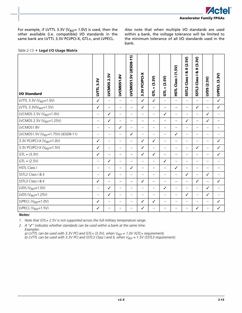
I/O Banks and CompatibilitySince each I/O bank has its own user-assigned inputreference voltage (VREF) and an input/output supplyvoltage (VCCI), only I/Os with compatible standards canbe assigned to the same bank.
Table 2-11 shows the compatible I/O standards for acommon VREF (for voltage-referenced standards).Similarly, Table 2-12 shows compatible standards for acommon VCCI.
Table 2-13 on page 2-13 summarizes the differentcombinations of voltages and I/O standards that can beused together in the same I/O bank. Note that two I/Ostandards are compatible if:
• Their VCCI values are identical.
• Their VREF standards are identical (if applicable).
Figure 2-3 • Use of an External Resistor for 5V Tolerance
Figure 2-4 • Bus Switch IDTQS32X2384
Non-Actel Part Actel FPGA5V 3.3V 3.3V
PCIclamp diode
Rext
5V 3.3V
3.3V
20X
5V
3. The user should note that in Bank 8 of both AX1000-FG484 and AX500-FG484, there are local violations of this 8:1 ratio.
Table 2-11 • Compatible I/O Standards for Different VREF Values
VREF Compatible Standards
1.5V SSTL 3 (Class I and II)
1.25V SSTL 2 (Class I and II)
1.0V GTL+ (2.5V and 3.3V Outputs)
0.75V HSTL (Class I)
Table 2-12 • Compatible I/O Standards for Different VCCI Values
VCCI1 Compatible Standards VREF
3.3V LVTTL, PCI, PCI-X, LVPECL, GTL+ 3.3V 1.0
3.3V SSTL 3 (Class I and II), LVTTL, PCI, LVPECL 1.5
2.5V LVCMOS 2.5V, GTL+ 2.5V, LVDS2 1.0
2.5V LVCMOS 2.5V, SSTL 2 (Classes I and II), LVDS2 1.25
1.8V LVCMOS 1.8V N/A
1.5V LVCMOS 1.5V, HSTL Class I 0.75
Notes:
1. VCCI is used for both inputs and outputs2. VCCI tolerance is ±5%
Axcelerator Family FPGAs
v2.6 2-13
For example, if LVTTL 3.3V (VREF= 1.0V) is used, then theother available (i.e. compatible) I/O standards in thesame bank are LVTTL 3.3V PCI/PCI-X, GTL+, and LVPECL.
Also note that when multiple I/O standards are usedwithin a bank, the voltage tolerance will be limited tothe minimum tolerance of all I/O standards used in thebank.
Table 2-13 • Legal I/O Usage Matrix
I/O Standard LVTT
L 3.
3V
LVC
MO
S 2.
5V
LVC
MO
S1.8
V
LVC
MO
S1.5
V (
JESD
8-11
)
3.3V
PC
I/PC
I-X
GTL
+ (
3.3V
)
GTL
+ (
2.5V
)
HST
L C
lass
I (1
.5V
)
SSTL
2 C
lass
I &
II (
2.5V
)
SSTL
3 C
lass
I &
II (
3.3V
)
LVD
S (2
.5V
)
LVPE
CL
(3.3
V)
LVTTL 3.3V (VREF=1.0V) – – – – – – – –
LVTTL 3.3V(VREF=1.5V) – – – – – – – –
LVCMOS 2.5V (VREF=1.0V) – – – – – – – – –
LVCMOS 2.5V (VREF=1.25V) – – – – – – – – –
LVCMOS1.8V – – – – – – – – – – –
LVCMOS1.5V (VREF=1.75V) (JESD8-11) – – – – – – – – – –
3.3V PCI/PCI-X (VREF=1.0V) – – – – – – – –
3.3V PCI/PCI-X (VREF=1.5V) – – – – – – – –
GTL + (3.3V) – – – – – – – –
GTL + (2.5V) – – – – – – – – – –
HSTL Class I – – – – – – – – – –
SSTL2 Class I & II – – – – – – – – –
SSTL3 Class I & II – – – – – – – –
LVDS (VREF=1.0V) – – – – – – – – –
LVDS (VREF=1.25V) – – – – – – – – –
LVPECL (VREF=1.0V) – – – – – – – –
LVPECL (VREF=1.5V) – – – – – – – –
Notes:
1. Note that GTL+ 2.5V is not supported across the full military temperature range.2. A "" indicates whether standards can be used within a bank at the same time.
Examples:a) LVTTL can be used with 3.3V PCI and GTL+ (3.3V), when VREF = 1.0V (GTL+ requirement).b) LVTTL can be used with 3.3V PCI and SSTL3 Class I and II, when VREF = 1.5V (SSTL3 requirement).
Axcelerator Family FPGAs
2-14 v2.6
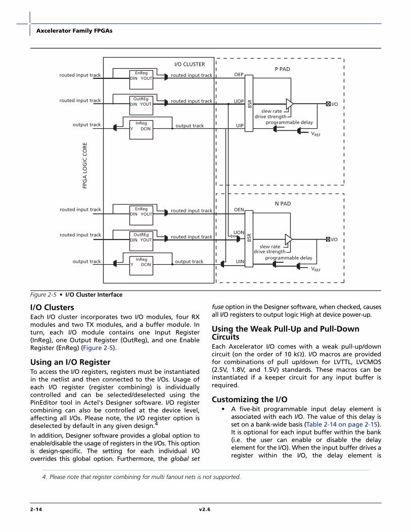
I/O ClustersEach I/O cluster incorporates two I/O modules, four RXmodules and two TX modules, and a buffer module. Inturn, each I/O module contains one Input Register(InReg), one Output Register (OutReg), and one EnableRegister (EnReg) (Figure 2-5).
Using an I/O RegisterTo access the I/O registers, registers must be instantiatedin the netlist and then connected to the I/Os. Usage ofeach I/O register (register combining) is individuallycontrolled and can be selected/deselected using thePinEditor tool in Actel's Designer software. I/O registercombining can also be controlled at the device level,affecting all I/Os. Please note, the I/O register option isdeselected by default in any given design.4
In addition, Designer software provides a global option toenable/disable the usage of registers in the I/Os. This optionis design-specific. The setting for each individual I/Ooverrides this global option. Furthermore, the global set
fuse option in the Designer software, when checked, causesall I/O registers to output logic High at device power-up.
Using the Weak Pull-Up and Pull-Down CircuitsEach Axcelerator I/O comes with a weak pull-up/downcircuit (on the order of 10 kΩ). I/O macros are providedfor combinations of pull up/down for LVTTL, LVCMOS(2.5V, 1.8V, and 1.5V) standards. These macros can beinstantiated if a keeper circuit for any input buffer isrequired.
Customizing the I/O• A five-bit programmable input delay element is
associated with each I/O. The value of this delay isset on a bank-wide basis (Table 2-14 on page 2-15).It is optional for each input buffer within the bank(i.e. the user can enable or disable the delayelement for the I/O). When the input buffer drives aregister within the I/O, the delay element is
Figure 2-5 • I/O Cluster Interface
EnRegDIN YOUT
Y DCIN
OutREgDIN YOUT
InReg
I/O CLUSTER
FPG
A L
OG
IC C
OR
E
OEP
UOP
UIPprogrammable delay
slew rateI/O
OEN
UON
UIN
drive strength
P PAD
N PADrouted input track
routed input track
output track
routed input track
routed input track
output track
routed input track
routed input track
output track
EnRegDIN YOUT
Y DCIN
OutREgDIN YOUT
InReg
routed input track
routed input track
output trackprogrammable delay
slew rateI/O
drive strength
VREF
VREF
BSR
BSR
4. Please note that register combining for multi fanout nets is not supported.
Axcelerator Family FPGAs
v2.6 2-15
activated by default to ensure a zero hold-time.The default setting for this property can be set inDesigner. When the input buffer does not drive aregister, the delay element is deactivated toprovide higher performance. Again, this can beoverridden by changing the default setting for thisproperty in Designer.
• The slew-rate value for the LVTTL output buffercan be programmed and can be set to either slowor fast.
• The drive strength value for LVTTL output bufferscan be programmed as well. There are fourdifferent drive strength values – 8mA, 12mA,16mA, or 24mA – that can be specified inDesigner.5
Using the Differential I/O StandardsDifferential I/O macros should be instantiated in thenetlist. The settings for these I/O standards cannot bechanged inside Designer. Please note that there are notristated or bidirectional I/O buffers for differentialstandards.
Using the Voltage-Referenced I/O StandardsUsing these I/O standards is similar to that of single-ended I/O standards. Their settings can be changed inDesigner.
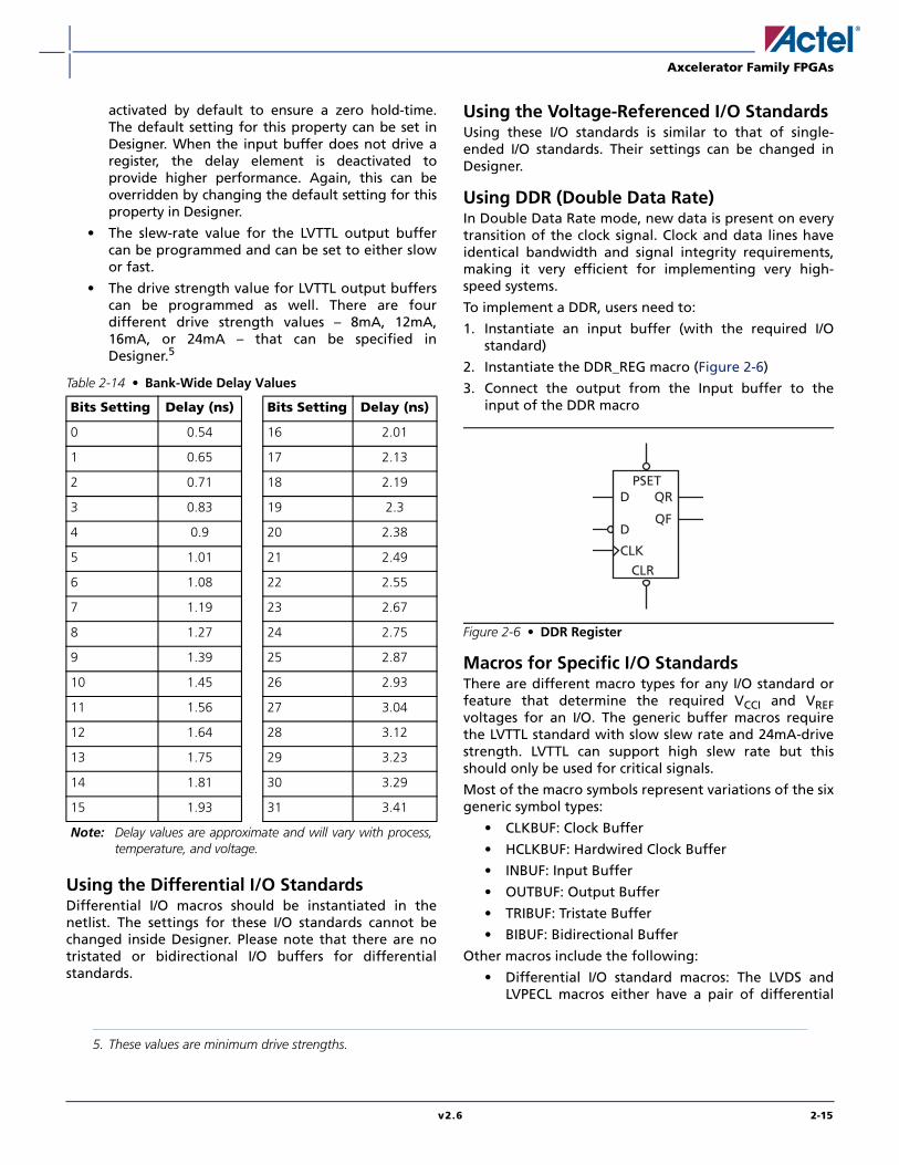
Using DDR (Double Data Rate)In Double Data Rate mode, new data is present on everytransition of the clock signal. Clock and data lines haveidentical bandwidth and signal integrity requirements,making it very efficient for implementing very high-speed systems.
To implement a DDR, users need to:
1. Instantiate an input buffer (with the required I/Ostandard)
2. Instantiate the DDR_REG macro (Figure 2-6)
3. Connect the output from the Input buffer to theinput of the DDR macro
Macros for Specific I/O StandardsThere are different macro types for any I/O standard orfeature that determine the required VCCI and VREFvoltages for an I/O. The generic buffer macros requirethe LVTTL standard with slow slew rate and 24mA-drivestrength. LVTTL can support high slew rate but thisshould only be used for critical signals.
Most of the macro symbols represent variations of the sixgeneric symbol types:
• CLKBUF: Clock Buffer
• HCLKBUF: Hardwired Clock Buffer
• INBUF: Input Buffer
• OUTBUF: Output Buffer
• TRIBUF: Tristate Buffer
• BIBUF: Bidirectional Buffer
Other macros include the following:
• Differential I/O standard macros: The LVDS andLVPECL macros either have a pair of differential
Table 2-14 • Bank-Wide Delay Values
Bits Setting Delay (ns) Bits Setting Delay (ns)
0 0.54 16 2.01
1 0.65 17 2.13
2 0.71 18 2.19
3 0.83 19 2.3
4 0.9 20 2.38
5 1.01 21 2.49
6 1.08 22 2.55
7 1.19 23 2.67
8 1.27 24 2.75
9 1.39 25 2.87
10 1.45 26 2.93
11 1.56 27 3.04
12 1.64 28 3.12
13 1.75 29 3.23
14 1.81 30 3.29
15 1.93 31 3.41
Note: Delay values are approximate and will vary with process,temperature, and voltage.
5. These values are minimum drive strengths.
Figure 2-6 • DDR Register
D QR
QFD
CLR
PSET
CLK
Axcelerator Family FPGAs
2-16 v2.6
inputs (e.g. INBUF_LVDS) or a pair of differentialoutputs (e.g. OUTBUF_LVPECL).
• Pull-up and pull-down variations of the INBUF,BIBUF, and TRIBUF macros. These are availableonly with TTL and LVCMOS thresholds. They canbe used to model the behavior of the pull-up andpull-down resistors available in the architecture.Whenever an input pin is left unconnected, theoutput pin will either go high or low rather thanunknown. This allows users to leave inputs
unconnected without having the negative effecton simulation of propagating unknowns.
• DDR_REG macro. It can be connected to any I/Ostandard input buffers (i.e. INBUF) to implement adouble data rate register. Designer software willmap it to the I/O module in the same way it mapsthe other registers to the I/O module.
Table 2-15, Table 2-16 on page 2-17, and Table 2-17 onpage 2-17 list all the available macro namesdifferentiated by I/O standard, type, slew rate, and drivestrength.
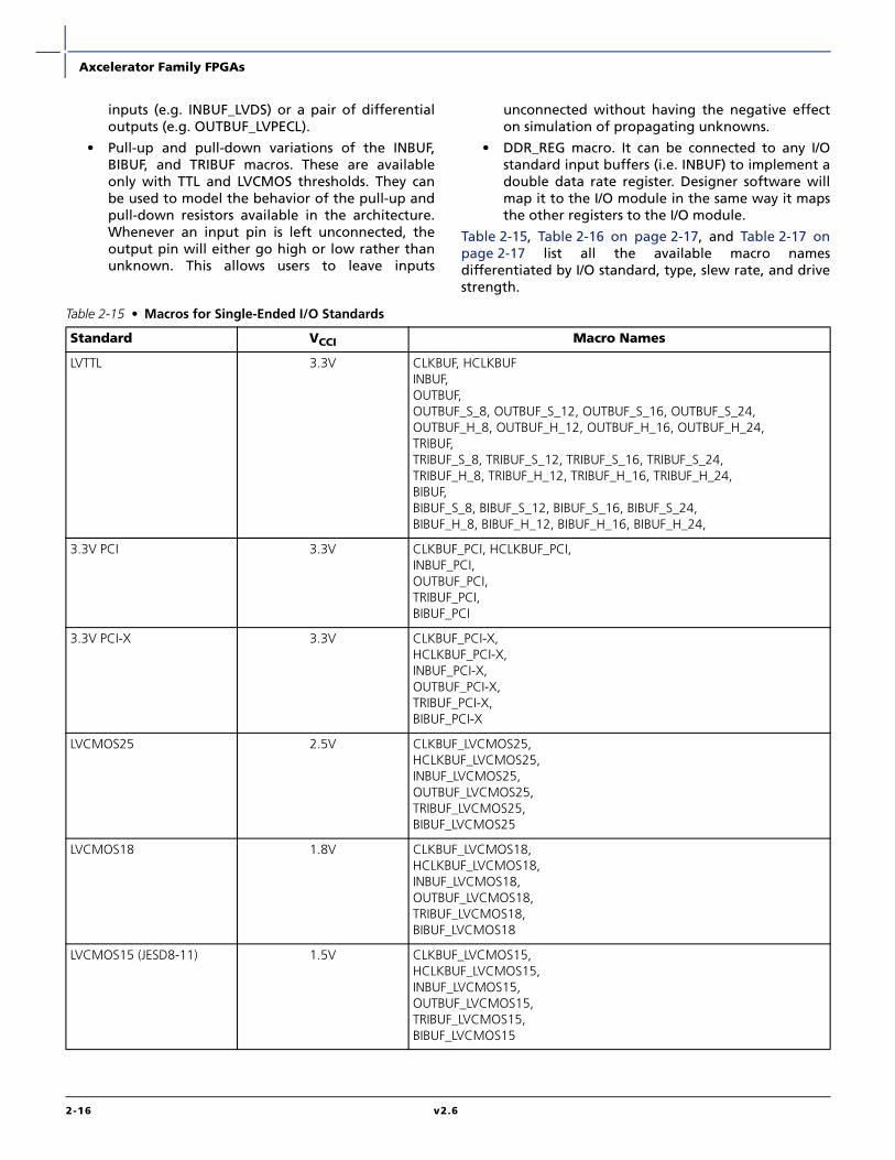
Table 2-15 • Macros for Single-Ended I/O Standards
Standard VCCI Macro Names
LVTTL 3.3V CLKBUF, HCLKBUFINBUF,OUTBUF,OUTBUF_S_8, OUTBUF_S_12, OUTBUF_S_16, OUTBUF_S_24,OUTBUF_H_8, OUTBUF_H_12, OUTBUF_H_16, OUTBUF_H_24,TRIBUF,TRIBUF_S_8, TRIBUF_S_12, TRIBUF_S_16, TRIBUF_S_24,TRIBUF_H_8, TRIBUF_H_12, TRIBUF_H_16, TRIBUF_H_24,BIBUF,BIBUF_S_8, BIBUF_S_12, BIBUF_S_16, BIBUF_S_24,BIBUF_H_8, BIBUF_H_12, BIBUF_H_16, BIBUF_H_24,
3.3V PCI 3.3V CLKBUF_PCI, HCLKBUF_PCI,INBUF_PCI,OUTBUF_PCI,TRIBUF_PCI,BIBUF_PCI
3.3V PCI-X 3.3V CLKBUF_PCI-X, HCLKBUF_PCI-X,INBUF_PCI-X,OUTBUF_PCI-X,TRIBUF_PCI-X,BIBUF_PCI-X
LVCMOS25 2.5V CLKBUF_LVCMOS25, HCLKBUF_LVCMOS25,INBUF_LVCMOS25,OUTBUF_LVCMOS25,TRIBUF_LVCMOS25,BIBUF_LVCMOS25
LVCMOS18 1.8V CLKBUF_LVCMOS18, HCLKBUF_LVCMOS18,INBUF_LVCMOS18,OUTBUF_LVCMOS18,TRIBUF_LVCMOS18,BIBUF_LVCMOS18
LVCMOS15 (JESD8-11) 1.5V CLKBUF_LVCMOS15, HCLKBUF_LVCMOS15,INBUF_LVCMOS15,OUTBUF_LVCMOS15,TRIBUF_LVCMOS15,BIBUF_LVCMOS15

Axcelerator Family FPGAs
v2.6 2-17
Table 2-16 • I/O Macros for Differential I/O Standards
Standard VCCI Macro Names
LVPECL 3.3V CLKBUF_LVPECL, HCLKBUF_LVPECL,INBUF_LVPECL, OUTBUF_LVPECL,
LVDS 2.5V CLKBUF_LVDS, HCLKBUF_LVDS,INBUF_LVDS, OUTBUF_LVDS,
Table 2-17 • I/O Macros for Voltage-Referenced I/O Standards
Standard VCCI VREF Macro Names
GTL+ 3.3V 1.0V CLKBUF_GTP33, HCLKBUF_GTP33, INBUF_GTP33, OUTBUF_GTP33, TRIBUF_GTP33,BIBUF_GTP33
GTL+ 2.5V 1.0V CLKBUF_GTP25, HCLKBUF_GTP25, INBUF_GTP25, OUTBUF_GTP25, TRIBUF_GTP25,BIBUF_GTP25
SSTL2 Class I 2.5V 1.25V CLKBUF_SSTL2_I, HCLKBUF_SSTL2_I, INBUF_SSTL2_I, OUTBUF_SSTL2_I,TRIBUF_SSTL2_I, BIBUF_SSTL2_I
SSTL2 Class II 2.5V 1.25V CLKBUF_SSTL2_II, HCLKBUF_SSTL2_II, INBUF_SSTL2_II, OUTBUF_SSTL2_II,TRIBUF_SSTL2_II, BIBUF_SSTL2_II
SSTL3 Class I 3.3V 1.5V CLKBUF_SSTL3_I, HCLKBUF_SSTL3_I, INBUF_SSTL3_I, OUTBUF_SSTL3_I,TRIBUF_SSTL3_I, BIBUF_SSTL3_I
SSTL3 Class II 3.3V 1.5V CLKBUF_SSTL3_II, HCLKBUF_SSTL3_II, INBUF_SSTL3_II, OUTBUF_SSTL3_II,TRIBUF_SSTL3_II, BIBUF_SSTL3_II
HSTL Class I 1.5V 0.75V CLKBUF_HSTL_I, HCLKBUF_HSTL_I, INBUF_HSTL_I, OUTBUF_HSTL_I, TRIBUF_HSTL_I,BIBUF_HSTL_I

Axcelerator Family FPGAs
2-18 v2.6
User I/O Naming ConventionsDue to the complex and flexible nature of the Axcelerator family’s user I/Os, a naming scheme is used to show thedetails of the I/O. The naming scheme explains to which bank an I/O belongs, as well as the pairing and pin polarity fordifferential I/Os (Figure 2-7).
Figure 2-7 • I/O Bank and Dedicated Pin Layout
Figure 2-8 • General Naming Schemes
PRC
PRD
PRB
PRA
TDO
TDI
TCK
TMS
TRSTLP
Corner4 Corner3
Corner1
I/O B
AN
K 3
I/O B
AN
K 2
I/O BANK 0
I/O BANK 5
I/O BANK 1
I/O BANK 4I/O
BA
NK
7I/O
BA
NK
6
Corner2
AX125 GNDVCCDA
GN
DV
CC
DA
VPU
MP
GNDVCCDA
GN
DV
CC
DA
VC
OM
PLG
VC
OM
PLH
VC
CPLG
VC
CPLH
VC
OM
PLB
VC
OM
PLA
VC
CPLB
VC
CPLA
VC
OM
PLE
VC
OM
PLF
VC
CPLE
VC
CPLF
VC
OM
PLD
VC
OM
PLC
VC
CPLD
VC
CPLC
GN
DV
CC
DA
GNDVCCDA
GNDVCCDA
GNDVCCDA
GNDVCCA
GNDVCCA
GN
DV
CC
A
GN
DV
CC
A
GNDVCCAGND
VCCA
GNDVCCI 2
GN
DV
CC
I 1
GN
DG
ND
VC
CI 5
GN
DV
CC
I 4
GNDVCCDA
GN
DV
CC
DA
GN
DV
CC
DA
GN
DV
CC
A
GN
DV
CC
A
GNDVCCI6
GNDVCCI7
GNDVCCI3
VC
CI 0
IOxxXBxFx
Fx refers to anunimplemented feature
and can be ignored.
Bank I/D 0 through 7,clockwise from IOB NW
P - Positive Pin/ N- Negative Pin
Pair number in thebank, starting at 00,
clockwise from IOB NW
IO12PB1F1 is the positive pin of the thirteenth pair of the first I/O bank (IOB NE). IO12PB1 combined with IO12NB1 form a differential pair. For those I/Os that can be employed either as a user I/O or as a special function, the following nomenclature is used:IOxxXBxFx/special_function_nameIOxxPB1Fx/xCLKx this pin can be configured as a clock input or as a user I/O.
Examples:

Axcelerator Family FPGAs
v2.6 2-19
I/O Standard Electrical Specifications
Table 2-18 • Input Capacitance
Symbol Parameter Conditions Min. Max. Units
CIN Input Capacitance VIN=0, f=1.0 MHz 10 pF
CINCLK Input Capacitance on Clock Pin VIN=0, f=1.0 MHz 10 pF
Figure 2-9 • Input Buffer Delays
Figure 2-10 • Output Buffer Delays
YININBUFPAD
ln
Y
GND
Input High
0V
VCCA
t DPt DP
VtripVtrip
50% 50%
(Rising) (Falling)
ln
ln
Out
GND50% 50%
TRIBUF
En
En
Out
GND50%
10%
50%En
Out
GND50% 50%
90%
To AC test loads (shown below)OUT Pad
VTTtENHZtENHZ
VOH
Vtrip
GND/VTT
VTT
VOL
tENLZ tENLZ
VCCI/VTT
VtripVtrip Vtrip
VOH
tPY tPY
(tDLH) (tDHL)
VCCA VCCAVCCA
VOL

Axcelerator Family FPGAs
2-20 v2.6
I/O Module Timing Characteristics
Figure 2-11 • Timing Model
Figure 2-12 • Input Register Timing Characteristics
OE
Out
IND
Q
CLK
OutReg
EnReg
InReg
D Q
Q
Q
D
D
CLK (Routed or Hardwired)
E
D
Q
CLR
PRESET
CLK
tSUE tHE
tSUD tHD
tICLKQ
tWASYN
tHASYN
tCLR
tREASYN
tCPWHL tCPWLH
tPRESET
tWASYN
tHASYN tREASYN
Axcelerator Family FPGAs
v2.6 2-21
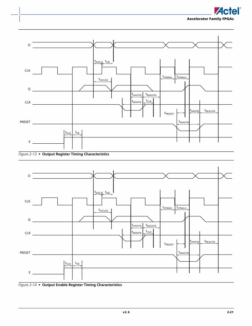
Figure 2-13 • Output Register Timing Characteristics
Figure 2-14 • Output Enable Register Timing Characteristics
E
D
Q
CLR
PRESET
CLK
tSUE tHE
tSUD tHD
tOCLKQ
tWASYN
tHASYN
tCLR
tREASYN
tCPWHL tCPWLH
tPRESET
tWASYN
tHASYN tREASYN
E
D
Q
CLR
PRESET
CLK
tSUE tHE
tSUD tHD
tOCLKQ
tWASYN
tHASYN
tCLR
tREASYN
tCPWHL tCPWLH
tPRESET
tWASYN
tHASYN tREASYN

Axcelerator Family FPGAs
2-22 v2.6
3.3V LVTTLLow-Voltage Transistor-Transistor Logic is a general purpose standard (EIA/JESD) for 3.3V applications. It uses an LVTTLinput buffer and push-pull output buffer.
AC Loadings
Timing Characteristics
Table 2-19 • DC Input and Output Levels
VIL VIH VOL VOH IOL IOH
Min,V Max,V Min,V Max,V Max,V Min,V mA mA
-0.3 0.8 2.0 3.6 0.4 2.4 24 –24
Figure 2-15 • AC Test Loads
Table 2-20 • AC Waveforms, Measuring Points, and Capacitive Load
Input Low (V) Input High (V) Measuring Point* (V) VREF (typ) (V) Cload (pF)
0 3.0 1.40 N/A 35
* Measuring Point = Vtrip
R to VCCI for tplz/tpzlR to GND for tphz/tpzh
35 pF for tpzh/tpzl
5 pF for tphz/tplz
Test Point Test Point
35 pFfor tristate
R=1k
for tpd
Table 2-21 • 3.3V LVTTL I/O ModuleWorst-Case Commercial Conditions VCCA = 1.425V, VCCI = 3.0V, TJ = 70°C
'–2' Speed '–1' Speed 'Std' Speed
Parameter Description Min. Max. Min. Max. Min. Max. Units
LVTTL Output Drive Strength = 1 (8mA) / Low Slew Rate
tDP Input Buffer 1.72 1.96 2.31 ns
tPY Output Buffer 14.32 16.31 19.19 ns
tICLKQ Clock-to-Q for the I/O input register 0.67 0.77 0.90 ns
tOCLKQ Clock-to-Q for the IO output register and the I/O enableregister
0.67 0.77 0.90 ns
tSUD Data Input Set-Up 0.23 0.27 0.31 ns
tSUE Enable Input Set-Up 0.26 0.30 0.35 ns
tHD Data Input Hold 0.00 0.00 0.00 ns
tHE Enable Input Hold 0.00 0.00 0.00 ns
tCPWHL Clock Pulse Width High to Low 0.43 0.48 0.57 ns
tCPWLH Clock Pulse Width Low to High 0.45 0.51 0.60 ns
tWASYN Asynchronous Pulse Width 0.43 0.48 0.57 ns
tREASYN Asynchronous Recovery Time 0.10 0.10 0.10 ns
tHASYN Asynchronous Removal Time 0.00 0.00 0.00 ns
tCLR Asynchronous Clear-to-Q 0.23 0.27 0.31 ns
tPRESET Asynchronous Preset-to-Q 0.23 0.27 0.31 ns

Axcelerator Family FPGAs
v2.6 2-23
LVTTL Output Drive Strength = 2 (12mA) / Low Slew Rate
tDP Input Buffer 1.72 1.96 2.31 ns
tPY Output Buffer 12.18 13.87 16.31 ns
tICLKQ Clock-to-Q for the I/O input register 0.67 0.77 0.90 ns
tOCLKQ Clock-to-Q for the IO output register and the I/O enableregister
0.67 0.77 0.90 ns
tSUD Data Input Set-Up 0.23 0.27 0.31 ns
tSUE Enable Input Set-Up 0.26 0.30 0.35 ns
tHD Data Input Hold 0.00 0.00 0.00 ns
tHE Enable Input Hold 0.00 0.00 0.00 ns
tCPWHL Clock Pulse Width High to Low 0.43 0.48 0.57 ns
tCPWLH Clock Pulse Width Low to High 0.45 0.51 0.60 ns
tWASYN Asynchronous Pulse Width 0.43 0.48 0.57 ns
tREASYN Asynchronous Recovery Time 0.10 0.10 0.10 ns
tHASYN Asynchronous Removal Time 0.00 0.00 0.00 ns
tCLR Asynchronous Clear-to-Q 0.23 0.27 0.31 ns
tPRESET Asynchronous Preset-to-Q 0.23 0.27 0.31 ns
LVTTL Output Drive Strength =3 (16mA) / Low Slew Rate
tDP Input Buffer 1.72 1.96 2.31 ns
tPY Output Buffer 11.07 12.61 14.83 ns
tICLKQ Clock-to-Q for the I/O input register 0.67 0.77 0.90 ns
tOCLKQ Clock-to-Q for the IO output register and the I/O enableregister
0.67 0.77 0.90 ns
tSUD Data Input Set-Up 0.23 0.27 0.31 ns
tSUE Enable Input Set-Up 0.26 0.30 0.35 ns
tHD Data Input Hold 0.00 0.00 0.00 ns
tHE Enable Input Hold 0.00 0.00 0.00 ns
tCPWHL Clock Pulse Width High to Low 0.43 0.48 0.57 ns
tCPWLH Clock Pulse Width Low to High 0.45 0.51 0.60 ns
tWASYN Asynchronous Pulse Width 0.43 0.48 0.57 ns
tREASYN Asynchronous Recovery Time 0.10 0.10 0.10 ns
tHASYN Asynchronous Removal Time 0.00 0.00 0.00 ns
tCLR Asynchronous Clear-to-Q 0.23 0.27 0.31 ns
tPRESET Asynchronous Preset-to-Q 0.23 0.27 0.31 ns
Table 2-21 • 3.3V LVTTL I/O ModuleWorst-Case Commercial Conditions VCCA = 1.425V, VCCI = 3.0V, TJ = 70°C (Continued)
'–2' Speed '–1' Speed 'Std' Speed
Parameter Description Min. Max. Min. Max. Min. Max. Units
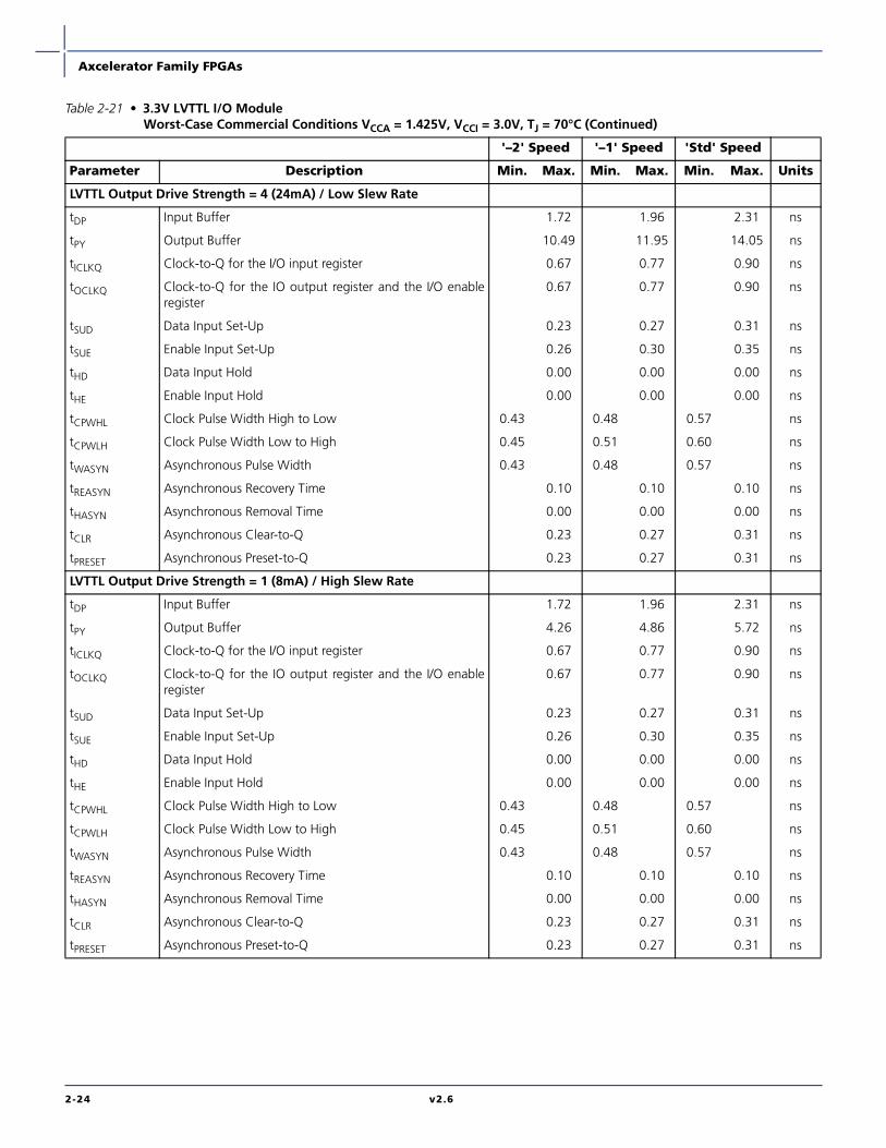
Axcelerator Family FPGAs
2-24 v2.6
LVTTL Output Drive Strength = 4 (24mA) / Low Slew Rate
tDP Input Buffer 1.72 1.96 2.31 ns
tPY Output Buffer 10.49 11.95 14.05 ns
tICLKQ Clock-to-Q for the I/O input register 0.67 0.77 0.90 ns
tOCLKQ Clock-to-Q for the IO output register and the I/O enableregister
0.67 0.77 0.90 ns
tSUD Data Input Set-Up 0.23 0.27 0.31 ns
tSUE Enable Input Set-Up 0.26 0.30 0.35 ns
tHD Data Input Hold 0.00 0.00 0.00 ns
tHE Enable Input Hold 0.00 0.00 0.00 ns
tCPWHL Clock Pulse Width High to Low 0.43 0.48 0.57 ns
tCPWLH Clock Pulse Width Low to High 0.45 0.51 0.60 ns
tWASYN Asynchronous Pulse Width 0.43 0.48 0.57 ns
tREASYN Asynchronous Recovery Time 0.10 0.10 0.10 ns
tHASYN Asynchronous Removal Time 0.00 0.00 0.00 ns
tCLR Asynchronous Clear-to-Q 0.23 0.27 0.31 ns
tPRESET Asynchronous Preset-to-Q 0.23 0.27 0.31 ns
LVTTL Output Drive Strength = 1 (8mA) / High Slew Rate
tDP Input Buffer 1.72 1.96 2.31 ns
tPY Output Buffer 4.26 4.86 5.72 ns
tICLKQ Clock-to-Q for the I/O input register 0.67 0.77 0.90 ns
tOCLKQ Clock-to-Q for the IO output register and the I/O enableregister
0.67 0.77 0.90 ns
tSUD Data Input Set-Up 0.23 0.27 0.31 ns
tSUE Enable Input Set-Up 0.26 0.30 0.35 ns
tHD Data Input Hold 0.00 0.00 0.00 ns
tHE Enable Input Hold 0.00 0.00 0.00 ns
tCPWHL Clock Pulse Width High to Low 0.43 0.48 0.57 ns
tCPWLH Clock Pulse Width Low to High 0.45 0.51 0.60 ns
tWASYN Asynchronous Pulse Width 0.43 0.48 0.57 ns
tREASYN Asynchronous Recovery Time 0.10 0.10 0.10 ns
tHASYN Asynchronous Removal Time 0.00 0.00 0.00 ns
tCLR Asynchronous Clear-to-Q 0.23 0.27 0.31 ns
tPRESET Asynchronous Preset-to-Q 0.23 0.27 0.31 ns
Table 2-21 • 3.3V LVTTL I/O ModuleWorst-Case Commercial Conditions VCCA = 1.425V, VCCI = 3.0V, TJ = 70°C (Continued)
'–2' Speed '–1' Speed 'Std' Speed
Parameter Description Min. Max. Min. Max. Min. Max. Units

Axcelerator Family FPGAs
v2.6 2-25
LVTTL Output Drive Strength = 2 (12mA) / High Slew Rate
tDP Input Buffer 1.72 1.96 2.31 ns
tPY Output Buffer 3.34 3.80 4.47 ns
tICLKQ Clock-to-Q for the I/O input register 0.67 0.77 0.90 ns
tOCLKQ Clock-to-Q for the IO output register and the I/O enableregister
0.67 0.77 0.90 ns
tSUD Data Input Set-Up 0.23 0.27 0.31 ns
tSUE Enable Input Set-Up 0.26 0.30 0.35 ns
tHD Data Input Hold 0.00 0.00 0.00 ns
tHE Enable Input Hold 0.00 0.00 0.00 ns
tCPWHL Clock Pulse Width High to Low 0.43 0.48 0.57 ns
tCPWLH Clock Pulse Width Low to High 0.45 0.51 0.60 ns
tWASYN Asynchronous Pulse Width 0.43 0.48 0.57 ns
tREASYN Asynchronous Recovery Time 0.10 0.10 0.10 ns
tHASYN Asynchronous Removal Time 0.00 0.00 0.00 ns
tCLR Asynchronous Clear-to-Q 0.23 0.27 0.31 ns
tPRESET Asynchronous Preset-to-Q 0.23 0.27 0.31 ns
LVTTL Output Drive Strength =3 (16mA) / High Slew Rate
tDP Input Buffer 1.72 1.96 2.31 ns
tPY Output Buffer 3.16 3.60 4.24 ns
tICLKQ Clock-to-Q for the I/O input register 0.67 0.77 0.90 ns
tOCLKQ Clock-to-Q for the IO output register and the I/O enableregister
0.67 0.77 0.90 ns
tSUD Data Input Set-Up 0.23 0.27 0.31 ns
tSUE Enable Input Set-Up 0.26 0.30 0.35 ns
tHD Data Input Hold 0.00 0.00 0.00 ns
tHE Enable Input Hold 0.00 0.00 0.00 ns
tCPWHL Clock Pulse Width High to Low 0.43 0.48 0.57 ns
tCPWLH Clock Pulse Width Low to High 0.45 0.51 0.60 ns
tWASYN Asynchronous Pulse Width 0.43 0.48 0.57 ns
tREASYN Asynchronous Recovery Time 0.10 0.10 0.10 ns
tHASYN Asynchronous Removal Time 0.00 0.00 0.00 ns
tCLR Asynchronous Clear-to-Q 0.23 0.27 0.31 ns
tPRESET Asynchronous Preset-to-Q 0.23 0.27 0.31 ns
Table 2-21 • 3.3V LVTTL I/O ModuleWorst-Case Commercial Conditions VCCA = 1.425V, VCCI = 3.0V, TJ = 70°C (Continued)
'–2' Speed '–1' Speed 'Std' Speed
Parameter Description Min. Max. Min. Max. Min. Max. Units

Axcelerator Family FPGAs
2-26 v2.6
LVTTL Output Drive Strength = 4 (24mA) / High Slew Rate
tDP Input Buffer 1.72 1.96 2.31 ns
tPY Output Buffer 3.03 3.45 4.06 ns
tICLKQ Clock-to-Q for the I/O input register 0.67 0.77 0.90 ns
tOCLKQ Clock-to-Q for the IO output register and the I/O enableregister
0.67 0.77 0.90 ns
tSUD Data Input Set-Up 0.23 0.27 0.31 ns
tSUE Enable Input Set-Up 0.26 0.30 0.35 ns
tHD Data Input Hold 0.00 0.00 0.00 ns
tHE Enable Input Hold 0.00 0.00 0.00 ns
tCPWHL Clock Pulse Width High to Low 0.43 0.48 0.57 ns
tCPWLH Clock Pulse Width Low to High 0.45 0.51 0.60 ns
tWASYN Asynchronous Pulse Width 0.43 0.48 0.57 ns
tREASYN Asynchronous Recovery Time 0.10 0.10 0.10 ns
tHASYN Asynchronous Removal Time 0.00 0.00 0.00 ns
tCLR Asynchronous Clear-to-Q 0.23 0.27 0.31 ns
tPRESET Asynchronous Preset-to-Q 0.23 0.27 0.31 ns
Table 2-21 • 3.3V LVTTL I/O ModuleWorst-Case Commercial Conditions VCCA = 1.425V, VCCI = 3.0V, TJ = 70°C (Continued)
'–2' Speed '–1' Speed 'Std' Speed
Parameter Description Min. Max. Min. Max. Min. Max. Units

Axcelerator Family FPGAs
v2.6 2-27
2.5V LVCMOS Low-Voltage Complementary Metal-Oxide Semiconductor for 2.5V is an extension of the LVCMOS standard (JESD8-5)used for general-purpose 2.5V applications. It uses a 3.3V tolerant CMOS input buffer and a push-pull output buffer.
AC Loadings
Timing Characteristics
Table 2-22 • DC Input and Output Levels
VIL VIH VOL VOH IOL IOH
Min,V Max,V Min,V Max,V Max,V Min,V mA mA
-0.3 0.7 1.7 3.6 0.4 2.0 12 -12
Figure 2-16 • AC Test Loads
Table 2-23 • AC Waveforms, Measuring Points, and Capacitive Loads
Input Low (V) Input High (V) Measuring Point* (V) VREF (typ) (V) Cload (pF)
0 2.5 1.25 N/A 35
* Measuring Point = Vtrip
R to VCCI for tplz/tpzlR to GND for tphz/tpzh
35 pF for tpzh/tpzl
5 pF for tphz/tplz
Test Point Test Point
35 pFfor tristate
R=1k
for tpd
Table 2-24 • 2.5V LVCMOS I/O ModuleWorst-Case Commercial Conditions VCCA = 1.425V, VCCI = 2.3V, TJ = 70°C
'–2' Speed '–1' Speed 'Std' Speed
Parameter Description Min. Max. Min. Max. Min. Max. Units
LVCMOS25 I/O Module Timing
tDP Input Buffer 1.99 2.26 2.66 ns
tPY Output Buffer 3.24 3.69 4.34 ns
tICLKQ Clock-to-Q for the I/O input register 0.67 0.77 0.90 ns
tOCLKQ Clock-to-Q for the IO output register and the I/Oenable register
0.67 0.77 0.90 ns
tSUD Data Input Set-Up 0.23 0.27 0.31 ns
tSUE Enable Input Set-Up 0.26 0.30 0.35 ns
tHD Data Input Hold 0.00 0.00 0.00 ns
tHE Enable Input Hold 0.00 0.00 0.00 ns
tCPWHL Clock Pulse Width High to Low 0.43 0.48 0.57 ns
tCPWLH Clock Pulse Width Low to High 0.45 0.51 0.60 ns
tWASYN Asynchronous Pulse Width 0.43 0.48 0.57 ns
tREASYN Asynchronous Recovery Time 0.10 0.10 0.10 ns
tHASYN Asynchronous Removal Time 0.00 0.00 0.00 ns
tCLR Asynchronous Clear-to-Q 0.23 0.27 0.31 ns
tPRESET Asynchronous Preset-to-Q 0.23 0.27 0.31 ns

Axcelerator Family FPGAs
2-28 v2.6
1.8V LVCMOSLow-Voltage Complementary Metal-Oxide Semiconductor for 1.8V is an extension of the LVCMOS standard (JESD8-5)used for general-purpose 1.8V applications. It uses a 3.3V tolerant CMOS input buffer and a push-pull output buffer.
AC Loadings
Timing Characteristics
Table 2-25 • DC Input and Output Levels
VIL VIH VOL VOH IOL IOH
Min,V Max,V Min,V Max,V Max,V Min,V mA mA
-0.3 0.2VCCI 0.7VCCI 3.6 0.2 VCCI-0.2 8mA -8mA
Figure 2-17 • AC Test Loads
Table 2-26 • AC Waveforms, Measuring Points, and Capacitive Loads
Input Low (V) Input High (V) Measuring Point* (V) VREF (typ) (V) Cload (pF)
0 1.8 0.5VCCI N/A 35
* Measuring Point = Vtrip
R to VCCI for tplz/tpzlR to GND for tphz/tpzh
35 pF for tpzh/tpzl
5 pF for tphz/tplz
Test Point Test Point
35 pFfor tristate
R=1k
for tpd
Table 2-27 • 1.8V LVCMOS I/O ModuleWorst-Case Commercial Conditions VCCA = 1.425V, VCCI = 1.7V, TJ = 70°C
'–2' Speed '–1' Speed 'Std' Speed
Parameter Description Min. Max. Min. Max. Min. Max. Units
LVCMOS18 Output Module Timing
tDP Input Buffer 3.30 3.76 4.42 ns
tPY Output Buffer 4.54 5.17 6.08 ns
tICLKQ Clock-to-Q for the I/O input register 0.67 0.77 0.90 ns
tOCLKQ Clock-to-Q for the IO output register and the I/Oenable register
0.67 0.77 0.90 ns
tSUD Data Input Set-Up 0.23 0.27 0.31 ns
tSUE Enable Input Set-Up 0.26 0.30 0.35 ns
tHD Data Input Hold 0.00 0.00 0.00 ns
tHE Enable Input Hold 0.00 0.00 0.00 ns
tCPWHL Clock Pulse Width High to Low 0.43 0.48 0.57 ns
tCPWLH Clock Pulse Width Low to High 0.45 0.51 0.60 ns
tWASYN Asynchronous Pulse Width 0.43 0.48 0.57 ns
tREASYN Asynchronous Recovery Time 0.10 0.10 0.10 ns
tHASYN Asynchronous Removal Time 0.00 0.00 0.00 ns
tCLR Asynchronous Clear-to-Q 0.23 0.27 0.31 ns
tPRESET Asynchronous Preset-to-Q 0.23 0.27 0.31 ns

Axcelerator Family FPGAs
v2.6 2-29
1.5V LVCMOS (JESD8-11)Low-Voltage Complementary Metal-Oxide Semiconductor for 1.5V is an extension of the LVCMOS standard (JESD8-5)used for general-purpose 1.5V applications. It uses a 3.3V tolerant CMOS input buffer and a push-pull output buffer.
AC Loadings
Timing Characteristics
Table 2-28 • DC Input and Output Levels
VIL VIH VOL VOH IOL IOH
Min,V Max,V Min,V Max,V Max,V Min,V mA mA
-0.5 0.35VCCI 0.65VCCI 3.6 0.4 VCCI-0.4 8mA -8mA
Table 2-29 • AC Test Loads
Table 2-30 • AC Waveforms, Measuring Points, and Capacitive Loads
Input Low (V) Input High (V) Measuring Point* (V) VREF (typ) (V) Cload (pF)
0 1.5 0.5VCCI N/A 35
* Measuring Point = Vtrip
R to VCCI for tplz/tpzlR to GND for tphz/tpzh
35 pF for tpzh/tpzl
5 pF for tphz/tplz
Test Point Test Point
35 pFfor tristate
R=1k
for tpd
Table 2-31 • 1.5V LVCMOS I/O ModuleWorst-Case Commercial Conditions VCCA = 1.425V, VCCI = 1.4V, TJ = 70°C
'–2' Speed '–1' Speed 'Std' Speed
Parameter Description Min. Max. Min. Max. Min. Max. Units
LVCMOS15 (JESD8-11) I/O Module Timing
tDP Input Buffer 3.63 4.14 4.87 ns
tPY Output Buffer 6.02 6.86 8.07 ns
tICLKQ Clock-to-Q for the I/O input register 0.67 0.77 0.90 ns
tOCLKQ Clock-to-Q for the IO output register and the I/Oenable register
0.67 0.77 0.90 ns
tSUD Data Input Set-Up 0.23 0.27 0.31 ns
tSUE Enable Input Set-Up 0.26 0.30 0.35 ns
tHD Data Input Hold 0.00 0.00 0.00 ns
tHE Enable Input Hold 0.00 0.00 0.00 ns
tCPWHL Clock Pulse Width High to Low 0.43 0.48 0.57 ns
tCPWLH Clock Pulse Width Low to High 0.45 0.51 0.60 ns
tWASYN Asynchronous Pulse Width 0.43 0.48 0.57 ns
tREASYN Asynchronous Recovery Time 0.10 0.10 0.10 ns
tHASYN Asynchronous Removal Time 0.00 0.00 0.00 ns
tCLR Asynchronous Clear-to-Q 0.23 0.27 0.31 ns
tPRESET Asynchronous Preset-to-Q 0.23 0.27 0.31 ns

Axcelerator Family FPGAs
2-30 v2.6
3.3V PCI, 3.3V PCI-XPeripheral Component Interface for 3.3V standard specifies support for both 33 MHz and 66 MHz PCI bus applications.It uses an LVTTL input buffer and a push-pull output buffer. The input and output buffers are 5V tolerant with the aidof external components. Axcelerator 3.3V PCI and 3.3V PCI-X buffers are compliant with the PCI Local Bus SpecificationRev. 2.1.
The PCI Compliance Specification requires the clamp diodes to be able to withstand for 11 ns, -3.5V in undershoot, and7.1V in overshoot.
AC Loadings
Table 2-32 • DC Input and Output Levels
VIL VIH VOL VOH IOL IOH
Min,V Max,V Min,V Max,V Max,V Min,V mA mA
PCI -0.5 0.3VCCI 0.5VCCI VCCI+0.5 (per PCI specification)
PCI-X -0.5 0.35VCCI 0.5VCCI VCCI+0.5 (per PCI specification)
Figure 2-18 • AC Test Loads
Table 2-33 • AC Waveforms, Measuring Points, and Capacitive Loads
Input Low (V) Input High (V) Measuring Point* (V) VREF (typ) (V) Cload (pF)
(Per PCI Spec and PCI-X Spec) N/A 10* Measuring Point = Vtrip
R to V for tpl R to GND for tph
CCI
10pF
GND
Test point for data
R=25
35 pF for tpzl/tpzh 5 pF for tphz/tplz
R to VCCI for tplz/tpzlR to GND for tphz/tpzh
Test Point for tristate
R=1k
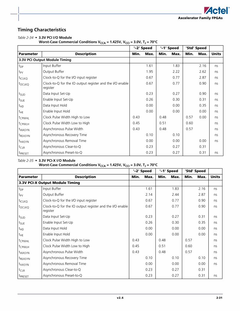
Axcelerator Family FPGAs
v2.6 2-31
Timing Characteristics
Table 2-34 • 3.3V PCI I/O ModuleWorst-Case Commercial Conditions VCCA = 1.425V, VCCI = 3.0V, TJ = 70°C
'–2' Speed '–1' Speed 'Std' Speed
Parameter Description Min. Max. Min. Max. Min. Max. Units
3.3V PCI Output Module Timing
tDP Input Buffer 1.61 1.83 2.16 ns
tPY Output Buffer 1.95 2.22 2.62 ns
tICLKQ Clock-to-Q for the I/O input register 0.67 0.77 2.87 ns
tOCLKQ Clock-to-Q for the IO output register and the I/O enableregister
0.67 0.77 0.90 ns
tSUD Data Input Set-Up 0.23 0.27 0.90 ns
tSUE Enable Input Set-Up 0.26 0.30 0.31 ns
tHD Data Input Hold 0.00 0.00 0.35 ns
tHE Enable Input Hold 0.00 0.00 0.00 ns
tCPWHL Clock Pulse Width High to Low 0.43 0.48 0.57 0.00 ns
tCPWLH Clock Pulse Width Low to High 0.45 0.51 0.60 ns
tWASYN Asynchronous Pulse Width 0.43 0.48 0.57 ns
tREASYN Asynchronous Recovery Time 0.10 0.10 ns
tHASYN Asynchronous Removal Time 0.00 0.00 0.00 ns
tCLR Asynchronous Clear-to-Q 0.23 0.27 0.31
tPRESET Asynchronous Preset-to-Q 0.23 0.27 0.31 ns
Table 2-35 • 3.3V PCI-X I/O ModuleWorst-Case Commercial Conditions VCCA = 1.425V, VCCI = 3.0V, TJ = 70°C
'–2' Speed '–1' Speed 'Std' Speed
Parameter Description Min. Max. Min. Max. Min. Max. Units
3.3V PCI-X Output Module Timing
tDP Input Buffer 1.61 1.83 2.16 ns
tPY Output Buffer 2.14 2.44 2.87 ns
tICLKQ Clock-to-Q for the I/O input register 0.67 0.77 0.90 ns
tOCLKQ Clock-to-Q for the IO output register and the I/O enableregister
0.67 0.77 0.90 ns
tSUD Data Input Set-Up 0.23 0.27 0.31 ns
tSUE Enable Input Set-Up 0.26 0.30 0.35 ns
tHD Data Input Hold 0.00 0.00 0.00 ns
tHE Enable Input Hold 0.00 0.00 0.00 ns
tCPWHL Clock Pulse Width High to Low 0.43 0.48 0.57 ns
tCPWLH Clock Pulse Width Low to High 0.45 0.51 0.60 ns
tWASYN Asynchronous Pulse Width 0.43 0.48 0.57 ns
tREASYN Asynchronous Recovery Time 0.10 0.10 0.10 ns
tHASYN Asynchronous Removal Time 0.00 0.00 0.00 ns
tCLR Asynchronous Clear-to-Q 0.23 0.27 0.31
tPRESET Asynchronous Preset-to-Q 0.23 0.27 0.31 ns

Axcelerator Family FPGAs
2-32 v2.6
Voltage-Referenced I/O Standards
GTL+Gunning Transceiver Logic Plus is a high-speed bus standard (JESD8-3). It requires a differential amplifier input bufferand an Open Drain output buffer. The VCCI pin should be connected to 2.5V or 3.3V. Note that 2.5V GTL+ is notsupported across the full military temperature range.
AC Loadings
Timing Characteristics
Table 2-36 • DC Input and Output Levels
VIL VIH VOL VOH IOL IOH
Min,V Max,V Min,V Max,V Max,V Min,V mA mA
N/A VREF-0.1 VREF+0.1 N/A 0.6 NA NA NA
Figure 2-19 • AC Test Loads
Table 2-37 • AC Waveforms, Measuring Points, and Capacitive Loads
Input Low (V) Input High (V) Measuring Point* (V) VREF (typ) (V) Cload (pF)
VREF-0.2 VREF+0.2 VREF 1.0 10* Measuring Point = Vtrip
Test Point
10 pF
25
VTT
Table 2-38 • 2.5V GTL+ I/O ModuleWorst-Case Commercial Conditions VCCA = 1.425V, VCCI = 2.3V, TJ = 70°C
'–2' Speed '–1' Speed 'Std' Speed
Parameter Description Min. Max. Min. Max. Min. Max. Units
2.5V GTL+ I/O Module Timing
tDP Input Buffer 1.75 1.99 2.35 ns
tPY Output Buffer 1.01 1.15 1.36 ns
tICLKQ Clock-to-Q for the I/O input register 0.67 0.77 0.90 ns
tOCLKQ Clock-to-Q for the IO output register and the I/O enableregister
0.67 0.77 0.90 ns
tSUD Data Input Set-Up 0.23 0.27 0.31 ns
tSUE Enable Input Set-Up 0.26 0.30 0.35 ns
tHD Data Input Hold 0.00 0.00 0.00 ns
tHE Enable Input Hold 0.00 0.00 0.00 ns
tCPWHL Clock Pulse Width High to Low 0.43 0.48 0.57 ns
tCPWLH Clock Pulse Width Low to High 0.45 0.51 0.60 ns
tWASYN Asynchronous Pulse Width 0.43 0.48 0.57 ns
tREASYN Asynchronous Recovery Time 0.10 0.10 0.10 ns
tHASYN Asynchronous Removal Time 0.00 0.00 0.00 ns
tCLR Asynchronous Clear-to-Q 0.23 0.27 0.31 ns
tPRESET Asynchronous Preset-to-Q 0.23 0.27 0.31 ns

Axcelerator Family FPGAs
v2.6 2-33
Table 2-39 • 3.3V GTL+ I/O ModuleWorst-Case Commercial Conditions VCCA = 1.425V, VCCI = 3.0V, TJ = 70°C
'–2' Speed '–1' Speed 'Std' Speed
Parameter Description Min. Max. Min. Max. Min. Max. Units
3.3V GTL+I/O Module Timing
tDP Input Buffer 1.75 1.99 2.35 ns
tPY Output Buffer 1.01 1.15 1.36 ns
tICLKQ Clock-to-Q for the I/O input register 0.67 0.77 0.90 ns
tOCLKQ Clock-to-Q for the IO output register and the I/Oenable register
0.67 0.77 0.90 ns
tSUD Data Input Set-Up 0.23 0.27 0.31 ns
tSUE Enable Input Set-Up 0.26 0.30 0.35 ns
tHD Data Input Hold 0.00 0.00 0.00 ns
tHE Enable Input Hold 0.00 0.00 0.00 ns
tCPWHL Clock Pulse Width High to Low 0.43 0.48 0.57 ns
tCPWLH Clock Pulse Width Low to High 0.45 0.51 0.60 ns
tWASYN Asynchronous Pulse Width 0.43 0.48 0.57 ns
tREASYN Asynchronous Recovery Time 0.10 0.10 0.10 ns
tHASYN Asynchronous Removal Time 0.00 0.00 0.00 ns
tCLR Asynchronous Clear-to-Q 0.23 0.27 0.31 ns
tPRESET Asynchronous Preset-to-Q 0.23 0.27 0.31 ns

Axcelerator Family FPGAs
2-34 v2.6
HSTL Class I High-Speed Transceiver Logic is a general-purpose high-speed 1.5V bus standard (EIA/JESD8-6). The Axcelerator devicessupport Class I. This requires a differential amplifier input buffer and a push-pull output buffer.
AC Loadings
Timing Characteristics
Table 2-40 • DC Input and Output Levels
VIL VIH VOL VOH IOL IOH
Min,V Max,V Min,V Max,V Max,V Min,V mA mA
-0.3 VREF-0.1 VREF+0.1 3.6 0.4 VCC-0.4 8 -8
Figure 2-20 • AC Test Loads
Table 2-41 • AC Waveforms, Measuring Points, and Capacitive Loads
Input Low (V) Input High (V) Measuring Point* (V) VREF (typ) (V) Cload (pF)
VREF-0.5 VREF+0.5 VREF 0.75 20
* Measuring Point = Vtrip
Test Point
20 pF
50
VTT
Table 2-42 • 1.5V HSTL Class I I/O ModuleWorst-Case Commercial Conditions VCCA = 1.425V, VCCI = 1.425V, TJ = 70°C
'–2' Speed '–1' Speed 'Std' Speed
Parameter Description Min. Max. Min. Max. Min. Max. Units
1.5V HSTL Class I I/O Module Timing
tDP Input Buffer 1.84 2.10 2.47 ns
tPY Output Buffer 4.93 5.62 6.61 ns
tICLKQ Clock-to-Q for the I/O input register 0.67 0.77 0.90 ns
tOCLKQ Clock-to-Q for the IO output register and the I/Oenable register
0.67 0.77 0.90 ns
tSUD Data Input Set-Up 0.23 0.27 0.31 ns
tSUE Enable Input Set-Up 0.26 0.30 0.35 ns
tHD Data Input Hold 0.00 0.00 0.00 ns
tHE Enable Input Hold 0.00 0.00 0.00 ns
tCPWHL Clock Pulse Width High to Low 0.43 0.48 0.57 ns
tCPWLH Clock Pulse Width Low to High 0.45 0.51 0.60 ns
tWASYN Asynchronous Pulse Width 0.43 0.48 0.57 ns
tREASYN Asynchronous Recovery Time 0.10 0.10 0.10 ns
tHASYN Asynchronous Removal Time 0.00 0.00 0.00 ns
tCLR Asynchronous Clear-to-Q 0.23 0.27 0.31 ns
tPRESET Asynchronous Preset-to-Q 0.23 0.27 0.31 ns
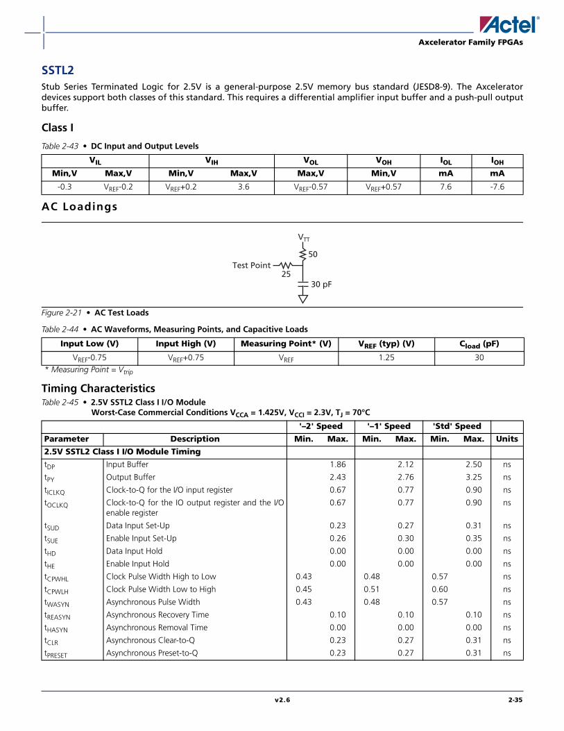
Axcelerator Family FPGAs
v2.6 2-35
SSTL2 Stub Series Terminated Logic for 2.5V is a general-purpose 2.5V memory bus standard (JESD8-9). The Axceleratordevices support both classes of this standard. This requires a differential amplifier input buffer and a push-pull outputbuffer.
Class I
AC Loadings
Timing Characteristics
Table 2-43 • DC Input and Output Levels
VIL VIH VOL VOH IOL IOH
Min,V Max,V Min,V Max,V Max,V Min,V mA mA
-0.3 VREF-0.2 VREF+0.2 3.6 VREF-0.57 VREF+0.57 7.6 -7.6
Figure 2-21 • AC Test Loads
Table 2-44 • AC Waveforms, Measuring Points, and Capacitive Loads
Input Low (V) Input High (V) Measuring Point* (V) VREF (typ) (V) Cload (pF)
VREF-0.75 VREF+0.75 VREF 1.25 30* Measuring Point = Vtrip
Test Point
30 pF
50
25
VTT
Table 2-45 • 2.5V SSTL2 Class I I/O ModuleWorst-Case Commercial Conditions VCCA = 1.425V, VCCI = 2.3V, TJ = 70°C
'–2' Speed '–1' Speed 'Std' Speed
Parameter Description Min. Max. Min. Max. Min. Max. Units
2.5V SSTL2 Class I I/O Module Timing
tDP Input Buffer 1.86 2.12 2.50 ns
tPY Output Buffer 2.43 2.76 3.25 ns
tICLKQ Clock-to-Q for the I/O input register 0.67 0.77 0.90 ns
tOCLKQ Clock-to-Q for the IO output register and the I/Oenable register
0.67 0.77 0.90 ns
tSUD Data Input Set-Up 0.23 0.27 0.31 ns
tSUE Enable Input Set-Up 0.26 0.30 0.35 ns
tHD Data Input Hold 0.00 0.00 0.00 ns
tHE Enable Input Hold 0.00 0.00 0.00 ns
tCPWHL Clock Pulse Width High to Low 0.43 0.48 0.57 ns
tCPWLH Clock Pulse Width Low to High 0.45 0.51 0.60 ns
tWASYN Asynchronous Pulse Width 0.43 0.48 0.57 ns
tREASYN Asynchronous Recovery Time 0.10 0.10 0.10 ns
tHASYN Asynchronous Removal Time 0.00 0.00 0.00 ns
tCLR Asynchronous Clear-to-Q 0.23 0.27 0.31 ns
tPRESET Asynchronous Preset-to-Q 0.23 0.27 0.31 ns

Axcelerator Family FPGAs
2-36 v2.6
Class II
AC Loadings
Timing Characteristics
Table 2-46 • DC Input and Output Levels
VIL VIH VOL VOH IOL IOH
Min,V Max,V Min,V Max,V Max,V Min,V mA mA
-0.3 VREF-0.2 VREF+0.2 3.6 VREF-0.8 VREF+0.8 15.2 -15.2
Figure 2-22 • AC Test Loads
Table 2-47 • AC Waveforms, Measuring Points, and Capacitive Loads
Input Low (V) Input High (V) Measuring Point* (V) VREF (typ) (V) Cload (pF)
VREF-0.75 VREF+0.75 VREF 1.25 30
* Measuring Point = Vtrip
Test Point
30 pF
25
25
VTT
Table 2-48 • 2.5V SSTL2 Class II I/O ModuleWorst-Case Commercial Conditions VCCA = 1.425V, VCCI = 2.3V, TJ = 70°C
'–2' Speed '–1' Speed 'Std' Speed
Parameter Description Min. Max. Min. Max. Min. Max. Units
2.5V SSTL2 Class II I/O Module Timing
tDP Input Buffer 1.93 2.20 2.59 ns
tPY Output Buffer 2.43 2.76 3.25 ns
tICLKQ Clock-to-Q for the I/O input register 0.67 0.77 0.90 ns
tOCLKQ Clock-to-Q for the IO output register and the I/Oenable register
0.67 0.77 0.90 ns
tSUD Data Input Set-Up 0.23 0.27 0.31 ns
tSUE Enable Input Set-Up 0.26 0.30 0.35 ns
tHD Data Input Hold 0.00 0.00 0.00 ns
tHE Enable Input Hold 0.00 0.00 0.00 ns
tCPWHL Clock Pulse Width High to Low 0.43 0.48 0.57 ns
tCPWLH Clock Pulse Width Low to High 0.45 0.51 0.60 ns
tWASYN Asynchronous Pulse Width 0.43 0.48 0.57 ns
tREASYN Asynchronous Recovery Time 0.10 0.10 0.10 ns
tHASYN Asynchronous Removal Time 0.00 0.00 0.00 ns
tCLR Asynchronous Clear-to-Q 0.23 0.27 0.31 ns
tPRESET Asynchronous Preset-to-Q 0.23 0.27 0.31 ns
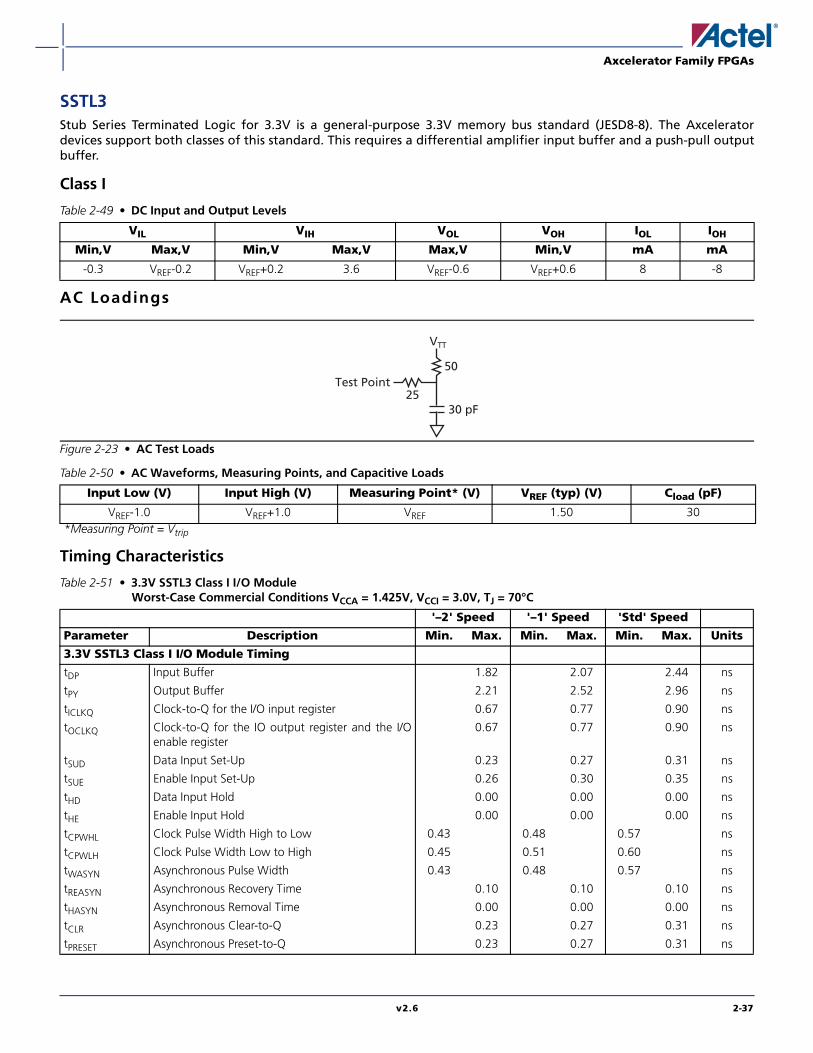
Axcelerator Family FPGAs
v2.6 2-37
SSTL3 Stub Series Terminated Logic for 3.3V is a general-purpose 3.3V memory bus standard (JESD8-8). The Axceleratordevices support both classes of this standard. This requires a differential amplifier input buffer and a push-pull outputbuffer.
Class I
AC Loadings
Timing Characteristics
Table 2-49 • DC Input and Output Levels
VIL VIH VOL VOH IOL IOH
Min,V Max,V Min,V Max,V Max,V Min,V mA mA
-0.3 VREF-0.2 VREF+0.2 3.6 VREF-0.6 VREF+0.6 8 -8
Figure 2-23 • AC Test Loads
Table 2-50 • AC Waveforms, Measuring Points, and Capacitive Loads
Input Low (V) Input High (V) Measuring Point* (V) VREF (typ) (V) Cload (pF)
VREF-1.0 VREF+1.0 VREF 1.50 30*Measuring Point = Vtrip
Test Point
30 pF
50
25
VTT
Table 2-51 • 3.3V SSTL3 Class I I/O ModuleWorst-Case Commercial Conditions VCCA = 1.425V, VCCI = 3.0V, TJ = 70°C
'–2' Speed '–1' Speed 'Std' Speed
Parameter Description Min. Max. Min. Max. Min. Max. Units
3.3V SSTL3 Class I I/O Module Timing
tDP Input Buffer 1.82 2.07 2.44 ns
tPY Output Buffer 2.21 2.52 2.96 ns
tICLKQ Clock-to-Q for the I/O input register 0.67 0.77 0.90 ns
tOCLKQ Clock-to-Q for the IO output register and the I/Oenable register
0.67 0.77 0.90 ns
tSUD Data Input Set-Up 0.23 0.27 0.31 ns
tSUE Enable Input Set-Up 0.26 0.30 0.35 ns
tHD Data Input Hold 0.00 0.00 0.00 ns
tHE Enable Input Hold 0.00 0.00 0.00 ns
tCPWHL Clock Pulse Width High to Low 0.43 0.48 0.57 ns
tCPWLH Clock Pulse Width Low to High 0.45 0.51 0.60 ns
tWASYN Asynchronous Pulse Width 0.43 0.48 0.57 ns
tREASYN Asynchronous Recovery Time 0.10 0.10 0.10 ns
tHASYN Asynchronous Removal Time 0.00 0.00 0.00 ns
tCLR Asynchronous Clear-to-Q 0.23 0.27 0.31 ns
tPRESET Asynchronous Preset-to-Q 0.23 0.27 0.31 ns

Axcelerator Family FPGAs
2-38 v2.6
Class II
AC Loadings
Timing Characteristics
Table 2-52 • DC Input and Output Levels
VIL VIH VOL VOH IOL IOH
Min,V Max,V Min,V Max,V Max,V Min,V mA mA
-0.3 VREF-0.2 VREF+0.2 3.6 VREF-0.8 VREF+0.8 16 -16
Figure 2-24 • AC Test Loads
Table 2-53 • AC Waveforms, Measuring Points, and Capacitive Loads
Input Low (V) Input High (V) Measuring Point* (V) VREF (typ) (V) Cload (pF)
VREF-1.0 VREF+1.0 VREF 1.50 30
* Measuring Point = Vtrip
Test Point
30 pF
25
25
VTT
Table 2-54 • 3.3V SSTL3 Class II I/O ModuleWorst-Case Commercial Conditions VCCA = 1.425V, VCCI = 3.0V, TJ = 70°C
'–2' Speed '–1' Speed 'Std' Speed
Parameter Description Min. Max. Min. Max. Min. Max. Units
3.3V SSTL3 Class II I/O Module Timing
tDP Input Buffer 1.88 2.14 2.53 ns
tPY Output Buffer 2.21 2.52 2.96 ns
tICLKQ Clock-to-Q for the I/O input register 0.67 0.77 0.90 ns
tOCLKQ Clock-to-Q for the IO output register and the I/Oenable register
0.67 0.77 0.90 ns
tSUD Data Input Set-Up 0.23 0.27 0.31 ns
tSUE Enable Input Set-Up 0.26 0.30 0.35 ns
tHD Data Input Hold 0.00 0.00 0.00 ns
tHE Enable Input Hold 0.00 0.00 0.00 ns
tCPWHL Clock Pulse Width High to Low 0.43 0.48 0.57 ns
tCPWLH Clock Pulse Width Low to High 0.45 0.51 0.60 ns
tWASYN Asynchronous Pulse Width 0.43 0.48 0.57 ns
tREASYN Asynchronous Recovery Time 0.10 0.10 0.10 ns
tHASYN Asynchronous Removal Time 0.00 0.00 0.00 ns
tCLR Asynchronous Clear-to-Q 0.23 0.27 0.31 ns
tPRESET Asynchronous Preset-to-Q 0.23 0.27 0.31 ns

Axcelerator Family FPGAs
v2.6 2-39
Differential Standards
Physical ImplementationImplementing differential I/O standards requires theconfiguration of a pair of external I/O pads, resulting in asingle internal signal. To facilitate construction of thedifferential pair, a single I/O Cluster contains theresources for a pair of I/Os. Configuration of the I/OCluster as a differential pair is handled by Actel'sDesigner software when the user instantiates adifferential I/O macro in the design.
Differential I/Os can also be used in conjunction with theembedded Input Register (InReg), Output Register
(OutReg), Enable Register (EnReg), and Double DataRate (DDR). However, there is no support forbidirectional I/Os or tristates with these standards.
LVDS Low-Voltage Differential Signal (ANSI/TIA/EIA-644) is ahigh-speed, differential I/O standard. It requires that onedata bit is carried through two signal lines, so two pinsare needed. It also requires an external resistortermination. The voltage swing between these twosignal lines is approximately 350 mV.
The LVDS circuit consists of a differential driverconnected to a terminated receiver through a constant-impedance transmission line. The receiver is a wide-common-mode-range differential amplifier. Thecommon-mode range is from 0.2V to 2.2V for adifferential input with 400 mV swing.
To implement the driver for the LVDS circuit, drivers fromtwo adjacent I/O cells are used to generate thedifferential signals (note that the driver is not a current-mode driver). This driver provides a nominal constant
current of 3.5 mA. When this current flows through a100 Ω termination resistor on the receiver side, a voltageswing of 350 mV is developed across the resistor. Thedirection of the current flow is controlled by the data fedto the driver.
An external-resistor network (three resistors) is neededto reduce the voltage swing to about 350 mV. Therefore,four external resistors are required, three for the driverand one for the receiver.
Figure 2-25 • LVDS Board-Level Implementation
140Ω 100Ω
ZO=50Ω
ZO=50Ω
165Ω
165Ω
+–
P
N
P
N
INBUF_LVDS
OUTBUF_LVDSFPGA FPGA
Table 2-55 • DC Input and Output Levels
DC Parameter Description Min. Typ. Max. Units
VCCI1 Supply Voltage 2.375 2.5 2.625 V
VOH Output High Voltage 1.25 1.425 1.6 V
VOL Output Low Voltage 0.9 1.075 1.25 V
VODIFF Differential Output Voltage 250 350 450 mV
VOCM Output Common Mode Voltage 1.125 1.25 1.375 V
VICM2 Input Common Mode Voltage 0.2 1.25 2.2 V
1. +/- 5%2. Differential input voltage =+/-350mV.

Axcelerator Family FPGAs
2-40 v2.6
Timing Characteristics
Table 2-56 • AC Waveforms, Measuring Points, and Capacitive Loads
Input Low (V) Input High (V) Measuring Point* (V)
1.2-0.125 1.2+0.125 1.2
* Measuring Point = Vtrip
Table 2-57 • LVDS I/O ModuleWorst-Case Commercial Conditions VCCA = 1.425V, VCCI = 2.3V, TJ = 70°C
'–2' Speed '–1' Speed 'Std' Speed
Parameter Description Min. Max. Min. Max. Min. Max. Units
LVDS Output Module Timing
tDP Input Buffer 1.84 2.10 2.47 ns
tPY Output Buffer 2.36 2.69 3.16 ns
tICLKQ Clock-to-Q for the I/O input register 0.67 0.77 0.90 ns
tOCLKQ Clock-to-Q for the IO output register and the I/Oenable register
0.67 0.77 0.90 ns
tSUD Data Input Set-Up 0.23 0.27 0.31 ns
tSUE Enable Input Set-Up 0.26 0.30 0.35 ns
tHD Data Input Hold 0.00 0.00 0.00 ns
tHE Enable Input Hold 0.00 0.00 0.00 ns
tCPWHL Clock Pulse Width High to Low 0.43 0.48 0.57 ns
tCPWLH Clock Pulse Width Low to High 0.45 0.51 0.60 ns
tWASYN Asynchronous Pulse Width 0.43 0.48 0.57 ns
tREASYN Asynchronous Recovery Time 0.10 0.10 0.10 ns
tHASYN Asynchronous Removal Time 0.00 0.00 0.00 ns
tCLR Asynchronous Clear-to-Q 0.23 0.27 0.31 ns
tPRESET Asynchronous Preset-to-Q 0.23 0.27 0.31 ns

Axcelerator Family FPGAs
v2.6 2-41
LVPECL Low-Voltage Positive Emitter-Coupled Logic (LVPECL) is another differential I/O standard. It requires that one data bitis carried through two signal lines. Like LVDS, two pins are needed. It also requires external resistor termination. Thevoltage swing between these two signal lines is approximately 850 mV.
The LVPECL circuit is similar to the LVDS scheme. It requires four external resistors, three for the driver and one for thereceiver. The values for the three driver resistors are different from that of LVDS since the output voltage levels aredifferent. Please note that the VOH levels are 200 mV below the standard LVPECL levels.
Figure 2-26 • LVPECL Board-Level Implementation
Table 2-58 • DC Input and Output Levels
DC Parameter
Min. Typ. Max.
UnitsMin. Max. Min. Max. Min. Max.
VCCI 3 3.3 3.6 V
VOH 1.8 2.11 1.92 2.28 2.13 2.41 V
VOL 0.96 1.27 1.06 1.43 1.3 1.57 V
VIH 1.49 2.72 1.49 2.72 1.49 2.72 V
VIL 0.86 2.125 0.86 2.125 0.86 2.125 V
Differential Input Voltage 0.3 0.3 0.3 V
Table 2-59 • AC Waveforms, Measuring Points, and Capacitive Loads
Input Low (V) Input High (V) Measuring Point* (V)
1.6-0.3 1.6+0.3 1.6
* Measuring Point = Vtrip
187Ω 100Ω
ZO=50Ω
ZO=50Ω
100Ω
100Ω
+
–
P
N
P
N
INBUF_LVPECL
OUTBUF_LVPECL
FPGA FPGA

Axcelerator Family FPGAs
2-42 v2.6
Timing Characteristics
Table 2-60 • LVPECL I/O ModuleWorst-Case Commercial Conditions VCCA = 1.425V, VCCI = 3.0V, TJ = 70°C
'–2' Speed '–1' Speed 'Std' Speed
Parameter Description Min. Max. Min. Max. Min. Max. Units
LVPECL Output Module Timing
tDP Input Buffer 1.70 1.93 2.28 ns
tPY Output Buffer 2.28 2.60 3.06 ns
tICLKQ Clock-to-Q for the I/O input register 0.67 0.77 0.90 ns
tOCLKQ Clock-to-Q for the IO output register and the I/Oenable register
0.67 0.77 0.90 ns
tSUD Data Input Set-Up 0.23 0.27 0.31 ns
tSUE Enable Input Set-Up 0.26 0.30 0.35 ns
tHD Data Input Hold 0.00 0.00 0.00 ns
tHE Enable Input Hold 0.00 0.00 0.00 ns
tCPWHL Clock Pulse Width High to Low 0.43 0.48 0.57 ns
tCPWLH Clock Pulse Width Low to High 0.45 0.51 0.60 ns
tWASYN Asynchronous Pulse Width 0.43 0.48 0.57 ns
tREASYN Asynchronous Recovery Time 0.10 0.10 0.10 ns
tHASYN Asynchronous Removal Time 0.00 0.00 0.00 ns
tCLR Asynchronous Clear-to-Q 0.23 0.27 0.31 ns
tPRESET Asynchronous Preset-to-Q 0.23 0.27 0.31 ns

Axcelerator Family FPGAs
v2.6 2-43
Module Specifications
C-Cell
IntroductionThe C-cell is one of the two logic module types in the AXarchitecture. It is the combinatorial logic resource in theAxcelerator device. The AX architecture implements anew combinatorial cell that is an extension of the C-cellimplemented in the SX-A family. The main enhancementof the new C-cell is the addition of carry-chain logic.
The C-cell can be used in a carry-chain mode to constructarithmetic functions. If carry-chain logic is not required,it can be disabled.
The C-cell features the following (Figure 2-27):
• Eight-input MUX (data: D0-D3, select: A0, A1, B0,B1). User signals can be routed to any one of theseinputs. Any of the C-cell inputs (D0-D3, A0, A1, B0,B1) can be tied to one of the four routed clocks(CLKE/F/G/H).
• Inverter (DB input) can be used to drive acomplement signal of any of the inputs to the C-cell.
• A carry input and a carry output. The carry inputsignal of the C-cell is the carry output from the C-cell directly to the north.
• Carry connect for carry-chain logic with a signalpropagation time of less than 0.1 ns.
• A hardwired connection (direct connect) to theadjacent R-cell (Register Cell) for all C-cells on theeast side of a SuperCluster with a signalpropagation time of less than 0.1 ns.
This layout of the C-cell (and the C-cell Cluster) enablesthe implementation of over 4,000 functions of up to fivebits. For example, two C-cells can be used together toimplement a four-input XOR function in a single celldelay.
The carry-chain configuration is handled automaticallyfor the user with Actel's extensive macro library (pleasesee Actel’s Antifuse Macro Library Guide for a completelisting of available Axcelerator macros)
.
Figure 2-27 • C-Cell
10
D1 D3 B1B0
D0 D2 DB A1A0
CFN FCI
FCO Y
0
0
00
1
1
11
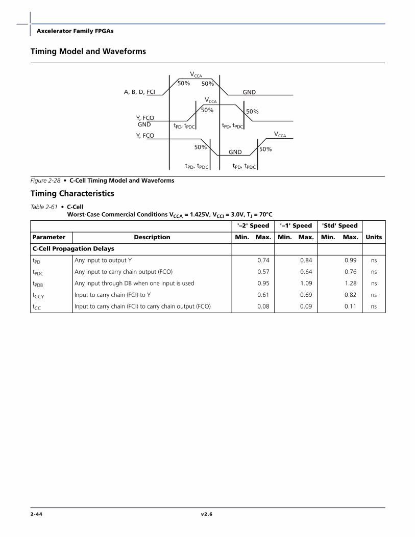
Axcelerator Family FPGAs
2-44 v2.6
Timing Model and Waveforms
Timing Characteristics
Figure 2-28 • C-Cell Timing Model and Waveforms
Y, FCO
Y, FCO
GND
VCCA
50% 50%
50% 50%
GND
GND50% 50%
A, B, D, FCI
tPD, tPDC
VCCA
VCCA
tPD, tPDC
tPD, tPDC tPD, tPDC
Table 2-61 • C-CellWorst-Case Commercial Conditions VCCA = 1.425V, VCCI = 3.0V, TJ = 70°C
'–2' Speed '–1' Speed 'Std' Speed
UnitsParameter Description Min. Max. Min. Max. Min. Max.
C-Cell Propagation Delays
tPD Any input to output Y 0.74 0.84 0.99 ns
tPDC Any input to carry chain output (FCO) 0.57 0.64 0.76 ns
tPDB Any input through DB when one input is used 0.95 1.09 1.28 ns
tCCY Input to carry chain (FCI) to Y 0.61 0.69 0.82 ns
tCC Input to carry chain (FCI) to carry chain output (FCO) 0.08 0.09 0.11 ns
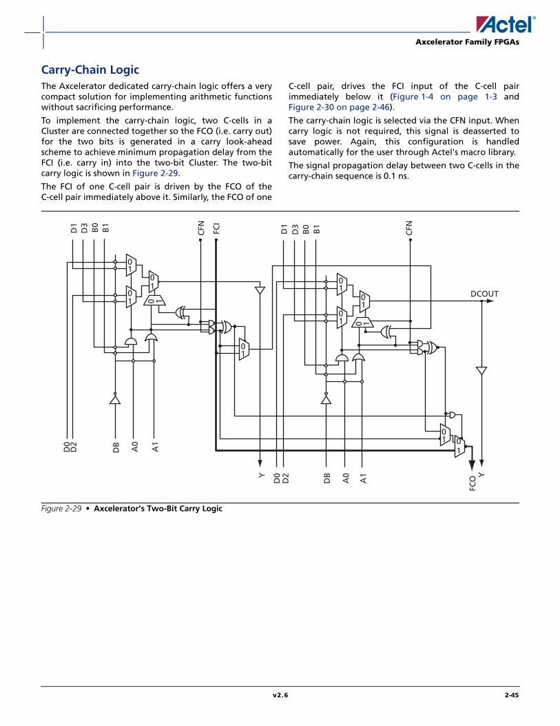
Axcelerator Family FPGAs
v2.6 2-45
Carry-Chain LogicThe Axcelerator dedicated carry-chain logic offers a verycompact solution for implementing arithmetic functionswithout sacrificing performance.
To implement the carry-chain logic, two C-cells in aCluster are connected together so the FCO (i.e. carry out)for the two bits is generated in a carry look-aheadscheme to achieve minimum propagation delay from theFCI (i.e. carry in) into the two-bit Cluster. The two-bitcarry logic is shown in Figure 2-29.
The FCI of one C-cell pair is driven by the FCO of theC-cell pair immediately above it. Similarly, the FCO of one
C-cell pair, drives the FCI input of the C-cell pairimmediately below it (Figure 1-4 on page 1-3 andFigure 2-30 on page 2-46).
The carry-chain logic is selected via the CFN input. Whencarry logic is not required, this signal is deasserted tosave power. Again, this configuration is handledautomatically for the user through Actel's macro library.
The signal propagation delay between two C-cells in thecarry-chain sequence is 0.1 ns.
Figure 2-29 • Axcelerator’s Two-Bit Carry Logic
10
10
10
10
10
10
10
10
10
10
10
DCOUT
D0
D2
DB
A1
A0
YFC
OY
D0
D2
DB
A1
A0
D1
D3
B1
B0D1
D3
B1
B0
CFN
CFNFC
I

Axcelerator Family FPGAs
2-46 v2.6
Timing CharacteristicsRefer to the Table 2-61 on page 2-44 for more information on carry-chain timing.
Note: The carry-chain sequence can end on either C-cell.Figure 2-30 • Carry-Chain Sequencing of C-cells
DCINDCOUT
C-cell1 C-cell2 DCOUT
R-cell1 DCIN
C-cell (2n-1)
C-cell2n DCOUT
R-celln CDIN
n-2 Clusters
FCO2n
FCI(2n-1)
FCI5
FCO4
FCI3FCO2
FCI1

Axcelerator Family FPGAs
v2.6 2-47
R-Cell
IntroductionThe R-cell, the sequential logic resource of theAxcelerator devices, is the second logic module type inthe AX family architecture. It includes clock inputs for alleight global resources of the Axcelerator architecture aswell as global presets and clears (Figure 2-31).
The main features of the R-cell include the following:
• Direct connection to the adjacent logic modulethrough the hardwired connection DCIN. DCIN isdriven by the DCOUT of an adjacent C-cell via theDirect-Connect routing resource, providing aconnection with less than 0.1 ns of routing delay.
• The R-cell can be used as a standalone flip-flop. Itcan be driven by any C-cell or I/O modules throughthe regular routing structure (using DIN as aroutable data input). This gives the option ofusing the R-Cell as a 2:1 MUXed flip-flop as well.
• Provision of data enable-input (S0).
• Independent active-low asynchronous clear (CLR).
• Independent active-low asynchronous preset(PSET). If both CLR and PSET are low, CLR hashigher priority.
• Clock can be driven by any of the following (CKPselects clock polarity):
– One of the four high performance hardwiredfast clocks (HCLKs)
– One of the four routed clocks (CLKs)
– User signals
• Global power-on clear (GCLR) and preset (GPSET),which drive each flip-flop on a chip-wide basis.
– When the Global Set Fuse option in theDesigner software is unchecked (by default),GCLR = 0 and GPSET =1 at device power-up.When the option is checked, GCLR = 1 andGPSET= 0. Both pins are pulled High when thedevice is in user mode.
• S0, S1, PSET, and CLR can be driven by routedclocks CLKE/F/G/H or user signals.
• DIN and S1 can be driven by user signals.
As with the C-cell, the configuration of the R-cell toperform various functions is handled automatically forthe user through Actel's extensive macro library (pleasesee Actel’s Antifuse Macro Library Guide for a completelisting of available AX macros).
Figure 2-31 • R-Cell
S1 S0
CK
P
CLR
GC
LR
PSET
GPS
ET
DCIN
DIN(user signals)
CK
S
Y
HCLKA/B/C/D
CLKE/F/G/H
Internal Logic

Axcelerator Family FPGAs
2-48 v2.6
Timing Models and Waveforms
Timing Characteristics
Figure 2-32 • R-Cell Delays
E
D
Q
CLR
PRESET
CLK
tSUE tHE
tSUD tHD
tRCO
tWASYN
tHASYN
tCLR
tREASYN
tCPWHL tCPWLH
tPRESET
tWASYN
tHASYN tREASYN
Table 2-62 • R-CellWorst-Case Commercial Conditions VCCA = 1.425V, VCCI = 3.0V, TJ = 70°C
'–2' Speed '–1' Speed 'Std' Speed
Parameter Description Min. Max. Min. Max. Min. Max. Units
R-Cell Propagation Delays
tRCO Sequential Clock-to-Q 0.67 0.77 0.90 ns
tCLR Asynchronous Clear-to-Q 0.23 0.27 0.31 ns
tPRESET Asynchronous Preset-to-Q 0.23 0.27 0.31 ns
tSUD Flip-Flop Data Input Set-Up 0.23 0.27 0.31 ns
tSUE Flip-Flop Enable Input Set-Up 0.26 0.30 0.35 ns
tHD Flip-Flop Data Input Hold 0.00 0.00 0.00 ns
tHE Flip-Flop Enable Input Hold 0.00 0.00 0.00 ns
tWASYN Asynchronous Pulse Width 0.43 0.48 0.57 ns
tREASYN Asynchronous Recovery Time 0.10 0.10 0.10 ns
tHASYN Asynchronous Removal Time 0.00 0.00 0.00 ns
tCPWHL Clock Pulse Width High to Low 0.42 0.47 0.55 ns
tCPWLH Clock Pulse Width Low to High 0.40 0.46 0.54 ns
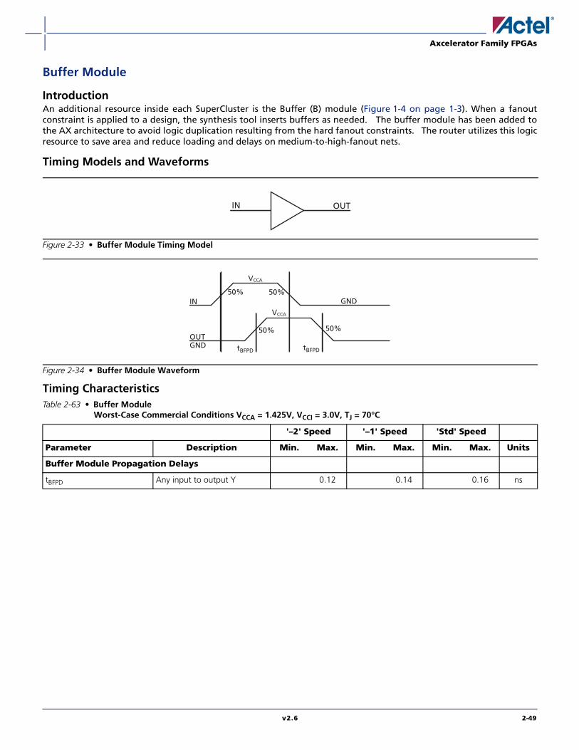
Axcelerator Family FPGAs
v2.6 2-49
Buffer Module
IntroductionAn additional resource inside each SuperCluster is the Buffer (B) module (Figure 1-4 on page 1-3). When a fanoutconstraint is applied to a design, the synthesis tool inserts buffers as needed. The buffer module has been added tothe AX architecture to avoid logic duplication resulting from the hard fanout constraints. The router utilizes this logicresource to save area and reduce loading and delays on medium-to-high-fanout nets.
Timing Models and Waveforms
Timing Characteristics
Figure 2-33 • Buffer Module Timing Model
Figure 2-34 • Buffer Module Waveform
Table 2-63 • Buffer ModuleWorst-Case Commercial Conditions VCCA = 1.425V, VCCI = 3.0V, TJ = 70°C
'–2' Speed '–1' Speed 'Std' Speed
Parameter Description Min. Max. Min. Max. Min. Max. Units
Buffer Module Propagation Delays
tBFPD Any input to output Y 0.12 0.14 0.16 ns
IN OUT
OUT
GND50% 50%
50% 50%
GND
IN
VCCA
VCCA
tBFPDtBFPD

Axcelerator Family FPGAs
2-50 v2.6
Routing Specifications
Routing ResourcesThe routing structure found in Axcelerator devicesenables any logic module to be connected to any otherlogic module while retaining high performance. Thereare multiple paths and routing resources that can beused to route one logic module to another, both within aSuperCluster and elsewhere on the chip.
There are four primary types of routing within the AXarchitecture: DirectConnect, CarryConnect, FastConnect,and Vertical and Horizontal Routing.
DirectConnectDirectConnects provide a high-speed connectionbetween an R-cell and its adjacent C-cell (Figure 2-35).This connection can be made from DCOUT of the C-cellto DCIN of the R-cell by configuring of the S1 line of theR-cell. This provides a connection that does not requirean antifuse and has a delay of less than 0.1 ns.
CarryConnectCarryConnects are used to build carry chains forarithmetic functions (Figure 2-35). The FCO output of theright C-cell of a two-C-cell Cluster drives the FCI input ofthe left C-cell in the two-C-cell Cluster immediatelybelow it. This pattern continues down both sides of eachSuperCluster column.
Similar to the DirectConnects, CarryConnects can be builtwithout an antifuse connection. This connection has adelay of less than 0.1 ns from the FCO of one two-C-cellcluster to the FCI of the two-C-cell cluster immediatelybelow it (see the "Carry-Chain Logic" on page 2-45 formore information).
FastConnectFor high-speed routing of logic signals, FastConnects canbe used to build a short distance connection using asingle antifuse (Figure 2-36 on page 2-51). FastConnectsprovide a maximum delay of 0.3 ns. The outputs of eachlogic module connect directly to the Output Trackswithin a SuperCluster. Signals on the Output Tracks can
then be routed through a single antifuse connection todrive the inputs of logic modules either within oneSuperCluster or in the SuperCluster immediately belowit.
Vertical and Horizontal Routing Vertical and Horizontal Tracks provide both local andlong distance routing (Figure 2-37 on page 2-51). Thesetracks are composed of both short-distance, segmentedrouting and across-chip routing tracks (segmented atcore tile boundaries). The short-distance, segmentedrouting resources can be concatenated through antifuseconnections to build longer routing tracks.
These short-distance routing tracks can be used withinand between SuperClusters or between modules of non-adjacent SuperClusters. They can be connected to theOutput Tracks and to any logic module input (R-cell,C-cell, Buffer, and TX module).
The across-chip horizontal and vertical routing provideslong-distance routing resources. These resourcesinterface with the rest of the routing structures through
Figure 2-35 • DirectConnect and CarryConnect

Axcelerator Family FPGAs
v2.6 2-51
the RX and TX modules (Figure 2-37). The RX module isused to drive signals from the across-chip horizontal andvertical routing to the Output Tracks within theSuperCluster. The TX module is used to drive vertical and
horizontal across-chip routing from either short-distancehorizontal tracks or from Output Tracks. The TX modulecan also be used to drive signals from vertical across-chiptracks to horizontal across-chip tracks and vice versa.
Figure 2-36 • FastConnect Routing
Figure 2-37 • Horizontal and Vertical Tracks

Axcelerator Family FPGAs
2-52 v2.6
Timing Characteristics
Table 2-64 • AX125 Predicted Routing DelaysWorst-Case Commercial Conditions VCCA = 1.425V, TJ = 70°C
'–2' Speed '–1' Speed 'Std' Speed
Parameter Description Typical Typical Typical Units
Predicted Routing Delays
tDC DirectConnect Routing Delay, FO1 0.11 0.12 0.15 ns
tFC FastConnect Routing Delay, FO1 0.35 0.39 0.46 ns
tRD1 Routing delay for FO1 0.35 0.40 0.47 ns
tRD2 Routing delay for FO2 0.38 0.43 0.51 ns
tRD3 Routing delay for FO3 0.43 0.48 0.57 ns
tRD4 Routing delay for FO4 0.48 0.55 0.64 ns
tRD5 Routing delay for FO5 0.55 0.62 0.73 ns
tRD6 Routing delay for FO6 0.64 0.72 0.85 ns
tRD7 Routing delay for FO7 0.79 0.89 1.05 ns
tRD8 Routing delay for FO8 0.88 0.99 1.17 ns
tRD16 Routing delay for FO16 1.49 1.69 1.99 ns
tRD32 Routing delay for FO32 2.32 2.63 3.10 ns
Table 2-65 • AX250 Predicted Routing DelaysWorst-Case Commercial Conditions VCCA = 1.425V, TJ = 70°C
'–2' Speed '–1' Speed 'Std' Speed
Parameter Description Typical Typical Typical Units
Predicted Routing Delays
tDC DirectConnect Routing Delay, FO1 0.11 0.12 0.15 ns
tFC FastConnect Routing Delay, FO1 0.35 0.39 0.46 ns
tRD1 Routing delay for FO1 0.39 0.45 0.53 ns
tRD2 Routing delay for FO2 0.41 0.46 0.54 ns
tRD3 Routing delay for FO3 0.48 0.55 0.64 ns
tRD4 Routing delay for FO4 0.56 0.63 0.75 ns
tRD5 Routing delay for FO5 0.60 0.68 0.80 ns
tRD6 Routing delay for FO6 0.84 0.96 1.13 ns
tRD7 Routing delay for FO7 0.90 1.02 1.20 ns
tRD8 Routing delay for FO8 1.00 1.13 1.33 ns
tRD16 Routing delay for FO16 2.17 2.46 2.89 ns
tRD32 Routing delay for FO32 3.55 4.03 4.74 ns

Axcelerator Family FPGAs
v2.6 2-53
Table 2-66 • AX500 Predicted Routing DelaysWorst-Case Commercial Conditions VCCA = 1.425V, TJ = 70°C
'–2' Speed '–1' Speed 'Std' Speed
Parameter Description Typical Typical Typical Units
Predicted Routing Delays
tDC DirectConnect Routing Delay, FO1 0.11 0.12 0.15 ns
tFC FastConnect Routing Delay, FO1 0.35 0.39 0.46 ns
tRD1 Routing delay for FO1 0.39 0.45 0.53 ns
tRD2 Routing delay for FO2 0.41 0.46 0.54 ns
tRD3 Routing delay for FO3 0.48 0.55 0.64 ns
tRD4 Routing delay for FO4 0.56 0.63 0.75 ns
tRD5 Routing delay for FO5 0.60 0.68 0.80 ns
tRD6 Routing delay for FO6 0.84 0.96 1.13 ns
tRD7 Routing delay for FO7 0.90 1.02 1.20 ns
tRD8 Routing delay for FO8 1.00 1.13 1.33 ns
tRD16 Routing delay for FO16 2.17 2.46 2.89 ns
tRD32 Routing delay for FO32 3.55 4.03 4.74 ns
Table 2-67 • AX1000 Predicted Routing DelaysWorst-Case Commercial Conditions VCCA = 1.425V, TJ = 70°C
'–2' Speed '–1' Speed 'Std' Speed
Parameter Description Typical Typical Typical Units
Predicted Routing Delays
tDC DirectConnect Routing Delay, FO1 0.12 0.13 0.15 ns
tFC FastConnect Routing Delay, FO1 0.35 0.39 0.46 ns
tRD1 Routing delay for FO1 0.45 0.51 0.60 ns
tRD2 Routing delay for FO2 0.53 0.60 0.71 ns
tRD3 Routing delay for FO3 0.56 0.63 0.74 ns
tRD4 Routing delay for FO4 0.63 0.71 0.84 ns
tRD5 Routing delay for FO5 0.73 0.82 0.97 ns
tRD6 Routing delay for FO6 0.99 1.13 1.32 ns
tRD7 Routing delay for FO7 1.02 1.15 1.36 ns
tRD8 Routing delay for FO8 1.48 1.68 1.97 ns
tRD16 Routing delay for FO16 2.57 2.91 3.42 ns
tRD32 Routing delay for FO32 4.24 4.81 5.65 ns

Axcelerator Family FPGAs
2-54 v2.6
Table 2-68 • AX2000 Predicted Routing DelaysWorst-Case Commercial Conditions VCCA = 1.425V, TJ = 70°C
'–2' Speed '–1' Speed 'Std' Speed
Parameter Description Typical Typical Typical Units
Predicted Routing Delays
tDC DirectConnect Routing Delay, FO1 0.12 0.13 0.15 ns
tFC FastConnect Routing Delay, FO1 0.35 0.39 0.46 ns
tRD1 Routing delay for FO1 0.50 0.56 0.66 ns
tRD2 Routing delay for FO2 0.59 0.67 0.79 ns
tRD3 Routing delay for FO3 0.70 0.80 0.94 ns
tRD4 Routing delay for FO4 0.76 0.87 1.02 ns
tRD5 Routing delay for FO5 0.98 1.11 1.31 ns
tRD6 Routing delay for FO6 1.48 1.68 1.97 ns
tRD7 Routing delay for FO7 1.65 1.87 2.20 ns
tRD8 Routing delay for FO8 1.73 1.96 2.31 ns
tRD16 Routing delay for FO16 2.58 2.92 3.44 ns
tRD32 Routing delay for FO32 4.24 4.81 5.65 ns

Axcelerator Family FPGAs
v2.6 2-55
Global ResourcesOne of the most important aspects of any FPGAarchitecture is its global resources or clocks. TheAxcelerator family provides the user with flexible andeasy-to-use global resources, without the limitationsnormally found in other FPGA architectures.
The AX architecture contains two types of globalresources, the HCLK (hardwired clock) and CLK (routedclock). Every Axcelerator device is provided with fourHCLKs and four CLKs for a total of eight clocks,regardless of device density.
Hardwired ClocksThe hardwired (HCLK) is a low-skew network that candirectly drive the clock inputs of all sequential modules(R-cells, I/O registers, and embedded RAM/FIFOs) in thedevice with no antifuse in the path. All four HCLKs areavailable everywhere on the chip.
Timing Characteristics
Table 2-69 • AX125 Dedicated (Hardwired) Array Clock NetworksWorst-Case Commercial Conditions VCCA = 1.425V, VCCI = 3.0V, TJ = 70°C
'–2' Speed '–1' Speed 'Std' Speed
Parameter Description Min. Max. Min. Max. Min. Max. Units
Dedicated (Hardwired) Array Clock Networks
tHCKL Input Low to High 3.02 3.44 4.05 ns
tHCKH Input High to Low 3.03 3.46 4.06 ns
tHPWH Minimum Pulse Width High 0.58 0.65 0.77 ns
tHPWL Minimum Pulse Width Low 0.52 0.59 0.69 ns
tHCKSW Maximum Skew 0.06 0.07 0.08 ns
tHP Minimum Period 1.15 1.31 1.54 ns
tHMAX Maximum Frequency 870 763 649 MHz
Table 2-70 • AX250 Dedicated (Hardwired) Array Clock NetworksWorst-Case Commercial Conditions VCCA = 1.425V, VCCI = 3.0V, TJ = 70°C
'–2' Speed '–1' Speed 'Std' Speed
Parameter Description Min. Max. Min. Max. Min. Max. Units
Dedicated (Hardwired) Array Clock Networks
tHCKL Input Low to High 2.57 2.93 3.45 ns
tHCKH Input High to Low 2.61 2.97 3.50 ns
tHPWH Minimum Pulse Width High 0.58 0.65 0.77 ns
tHPWL Minimum Pulse Width Low 0.52 0.59 0.69 ns
tHCKSW Maximum Skew 0.06 0.07 0.08 ns
tHP Minimum Period 1.15 1.31 1.54 ns
tHMAX Maximum Frequency 870 763 649 MHz
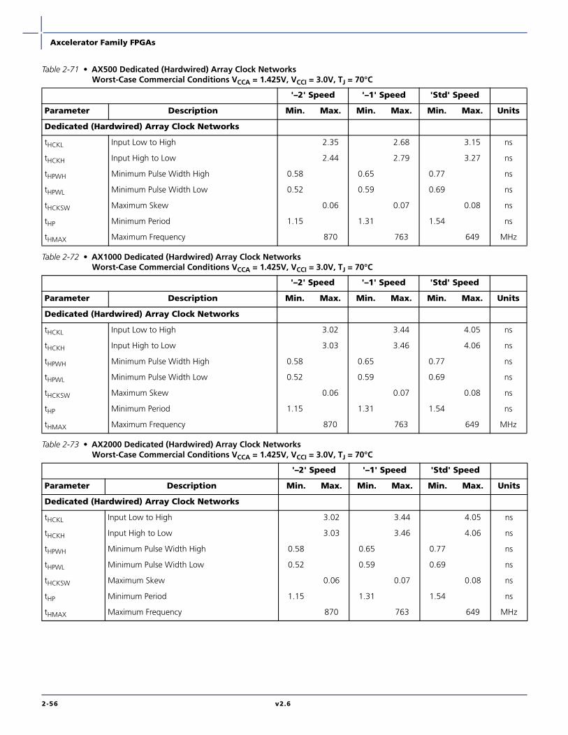
Axcelerator Family FPGAs
2-56 v2.6
Table 2-71 • AX500 Dedicated (Hardwired) Array Clock NetworksWorst-Case Commercial Conditions VCCA = 1.425V, VCCI = 3.0V, TJ = 70°C
'–2' Speed '–1' Speed 'Std' Speed
Parameter Description Min. Max. Min. Max. Min. Max. Units
Dedicated (Hardwired) Array Clock Networks
tHCKL Input Low to High 2.35 2.68 3.15 ns
tHCKH Input High to Low 2.44 2.79 3.27 ns
tHPWH Minimum Pulse Width High 0.58 0.65 0.77 ns
tHPWL Minimum Pulse Width Low 0.52 0.59 0.69 ns
tHCKSW Maximum Skew 0.06 0.07 0.08 ns
tHP Minimum Period 1.15 1.31 1.54 ns
tHMAX Maximum Frequency 870 763 649 MHz
Table 2-72 • AX1000 Dedicated (Hardwired) Array Clock NetworksWorst-Case Commercial Conditions VCCA = 1.425V, VCCI = 3.0V, TJ = 70°C
'–2' Speed '–1' Speed 'Std' Speed
Parameter Description Min. Max. Min. Max. Min. Max. Units
Dedicated (Hardwired) Array Clock Networks
tHCKL Input Low to High 3.02 3.44 4.05 ns
tHCKH Input High to Low 3.03 3.46 4.06 ns
tHPWH Minimum Pulse Width High 0.58 0.65 0.77 ns
tHPWL Minimum Pulse Width Low 0.52 0.59 0.69 ns
tHCKSW Maximum Skew 0.06 0.07 0.08 ns
tHP Minimum Period 1.15 1.31 1.54 ns
tHMAX Maximum Frequency 870 763 649 MHz
Table 2-73 • AX2000 Dedicated (Hardwired) Array Clock NetworksWorst-Case Commercial Conditions VCCA = 1.425V, VCCI = 3.0V, TJ = 70°C
'–2' Speed '–1' Speed 'Std' Speed
Parameter Description Min. Max. Min. Max. Min. Max. Units
Dedicated (Hardwired) Array Clock Networks
tHCKL Input Low to High 3.02 3.44 4.05 ns
tHCKH Input High to Low 3.03 3.46 4.06 ns
tHPWH Minimum Pulse Width High 0.58 0.65 0.77 ns
tHPWL Minimum Pulse Width Low 0.52 0.59 0.69 ns
tHCKSW Maximum Skew 0.06 0.07 0.08 ns
tHP Minimum Period 1.15 1.31 1.54 ns
tHMAX Maximum Frequency 870 763 649 MHz

Axcelerator Family FPGAs
v2.6 2-57
Routed ClocksThe routed clock (CLK) is a low-skew network that candrive the clock inputs of all sequential modules in thedevice (logically equivalent to the HCLK), but has theadded flexibility in that it can drive the S0 (Enable), S1,PSET, and CLR input of a register (R-cells and I/O
registers) as well as any of the inputs of any C-cell in thedevice. This allows CLKs to be used not only as clocks, butalso for other global signals or high fanout nets. All fourCLKs are available everywhere on the chip.
Timing Characteristics
Table 2-74 • AX125 Routed Array Clock NetworksWorst-Case Commercial Conditions VCCA = 1.425V, VCCI = 3.0V, TJ = 70°C
'–2' Speed '–1' Speed 'Std' Speed
Parameter Description Min. Max. Min. Max. Min. Max. Units
Routed Array Clock Networks
tRCKL Input Low to High 3.08 3.50 4.12 ns
tRCKH Input High to Low 3.13 3.56 4.19 ns
tRPWH Minimum Pulse Width High 0.57 0.64 0.75 ns
tRPWL Minimum Pulse Width Low 0.52 0.59 0.69 ns
tRCKSW Maximum Skew 0.35 0.39 0.46 ns
tRP Minimum Period 1.15 1.31 1.54 ns
tRMAX Maximum Frequency 870 763 649 MHz
Table 2-75 • AX250 Routed Array Clock NetworksWorst-Case Commercial Conditions VCCA = 1.425V, VCCI = 3.0V, TJ = 70°C
'–2' Speed '–1' Speed 'Std' Speed
Parameter Description Min. Max. Min. Max. Min. Max. Units
Routed Array Clock Networks
tRCKL Input Low to High 2.52 2.87 3.37 ns
tRCKH Input High to Low 2.59 2.95 3.47 ns
tRPWH Minimum Pulse Width High 0.57 0.64 0.75 ns
tRPWL Minimum Pulse Width Low 0.52 0.59 0.69 ns
tRCKSW Maximum Skew 0.35 0.39 0.46 ns
tRP Minimum Period 1.15 1.31 1.54 ns
tRMAX Maximum Frequency 870 763 649 MHz

Axcelerator Family FPGAs
2-58 v2.6
Table 2-76 • AX500 Routed Array Clock NetworksWorst-Case Commercial Conditions VCCA = 1.425V, VCCI = 3.0V, TJ = 70°C
'–2' Speed '–1' Speed 'Std' Speed
Parameter Description Min. Max. Min. Max. Min. Max. Units
Routed Array Clock Networks
tRCKL Input Low to High 2.31 2.63 3.09 ns
tRCKH Input High to Low 2.44 2.78 3.27 ns
tRPWH Minimum Pulse Width High 0.57 0.64 0.75 ns
tRPWL Minimum Pulse Width Low 0.52 0.59 0.69 ns
tRCKSW Maximum Skew 0.35 0.39 0.46 ns
tRP Minimum Period 1.15 1.31 1.54 ns
tRMAX Maximum Frequency 870 763 649 MHz
Table 2-77 • AX1000 Routed Array Clock NetworksWorst-Case Commercial Conditions VCCA = 1.425V, VCCI = 3.0V, TJ = 70°C
'–2' Speed '–1' Speed 'Std' Speed
Parameter Description Min. Max. Min. Max. Min. Max. Units
Routed Array Clock Networks
tRCKL Input Low to High 3.08 3.50 4.12 ns
tRCKH Input High to Low 3.13 3.56 4.19 ns
tRPWH Minimum Pulse Width High 0.57 0.64 0.75 ns
tRPWL Minimum Pulse Width Low 0.52 0.59 0.69 ns
tRCKSW Maximum Skew 0.35 0.39 0.46 ns
tRP Minimum Period 1.15 1.31 1.54 ns
tRMAX Maximum Frequency 870 763 649 MHz
Table 2-78 • AX2000 Routed Array Clock NetworksWorst-Case Commercial Conditions VCCA = 1.425V, VCCI = 3.0V, TJ = 70°C
'–2' Speed '–1' Speed 'Std' Speed
Parameter Description Min. Max. Min. Max. Min. Max. Units
Routed Array Clock Networks
tRCKL Input Low to High 3.08 3.50 4.12 ns
tRCKH Input High to Low 3.13 3.56 4.19 ns
tRPWH Minimum Pulse Width High 0.57 0.64 0.75 ns
tRPWL Minimum Pulse Width Low 0.52 0.59 0.69 ns
tRCKSW Maximum Skew 0.35 0.39 0.46 ns
tRP Minimum Period 1.15 1.31 1.54 ns
tRMAX Maximum Frequency 870 763 649 MHz
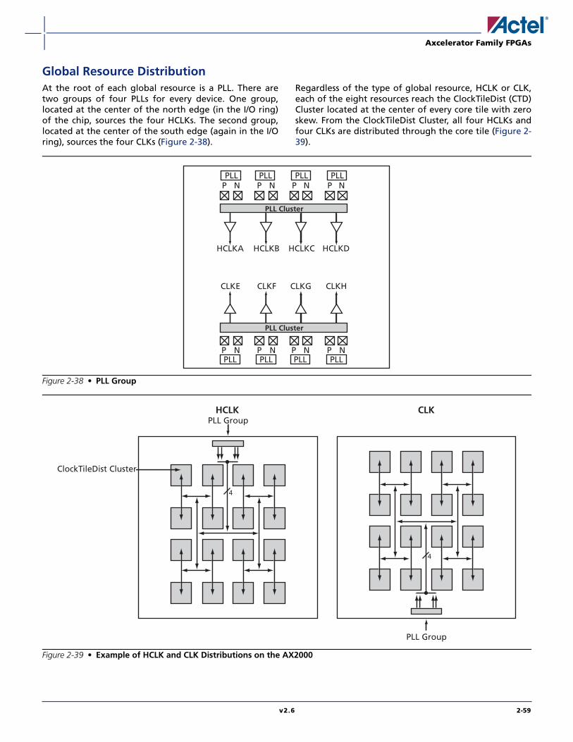
Axcelerator Family FPGAs
v2.6 2-59
Global Resource DistributionAt the root of each global resource is a PLL. There aretwo groups of four PLLs for every device. One group,located at the center of the north edge (in the I/O ring)of the chip, sources the four HCLKs. The second group,located at the center of the south edge (again in the I/Oring), sources the four CLKs (Figure 2-38).
Regardless of the type of global resource, HCLK or CLK,each of the eight resources reach the ClockTileDist (CTD)Cluster located at the center of every core tile with zeroskew. From the ClockTileDist Cluster, all four HCLKs andfour CLKs are distributed through the core tile (Figure 2-39).
Figure 2-38 • PLL Group
Figure 2-39 • Example of HCLK and CLK Distributions on the AX2000
PLL Cluster
PLL Cluster
P N P N P N P N
P N P N P N P N
HCLKA HCLKB HCLKC HCLKD
CLKE
PLL
CLKF CLKG CLKH
PLL PLL PLL
PLL PLL PLL PLL
PLL GroupHCLK CLK
PLL Group
4
4
ClockTileDist Cluster

Axcelerator Family FPGAs
2-60 v2.6
The ClockTileDist Cluster contains an HCLKMux (HM)module for each of the four HCLK trees and a CLKMux(CM) module for each of the CLK trees. The HCLKbranches then propagate horizontally through themiddle of the core tile to HCLKColDist (HD) modules inevery SuperCluster column. The CLK branches propagate
vertically through the center of the core tile toCLKRowDist (RD) modules in every SuperCluster row.Together, the HCLK and CLK branches provide for a low-skew global fanout within the core tile (Figure 2-40 andFigure 2-41).
Figure 2-40 • CTD, CD, and HD Module Layout
Figure 2-41 • HCLK and CLK Distribution within a Core Tile
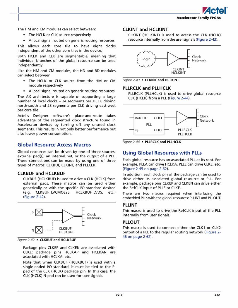
Axcelerator Family FPGAs
v2.6 2-61
The HM and CM modules can select between:
• The HCLK or CLK source respectively
• A local signal routed on generic routing resources
This allows each core tile to have eight clocksindependent of the other core tiles in the device.
Both HCLK and CLK are segmentable, meaning thatindividual branches of the global resource can be usedindependently.
Like the HM and CM modules, the HD and RD modulescan select between:
• The HCLK or CLK source from the HM or CMmodule respectively
• A local signal routed on generic routing resources
The AX architecture is capable of supporting a largenumber of local clocks – 24 segments per HCLK drivingnorth-south and 28 segments per CLK driving east-westper core tile.
Actel's Designer software’s place-and-route takesadvantage of the segmented clock structure found inAxcelerator devices by turning off any unused clocksegments. This results in not only better performance butalso lower power consumption.
Global Resource Access MacrosGlobal resources can be driven by one of three sources:external pad(s), an internal net, or the output of a PLL.These connections can be made by using one of threetypes of macros: CLKBUF, CLKINT, and PLLCLK.
CLKBUF and HCLKBUFCLKBUF (HCLKBUF) is used to drive a CLK (HCLK) fromexternal pads. These macros can be used eithergenerically or with the specific I/O standard desired(e.g. CLKBUF_LVCMOS25, HCLKBUF_LVDS, etc.)(Figure 2-42).
Package pins CLKEP and CLKEN are associated withCLKE; package pins HCLKAP and HCLKAN areassociated with HCLKA, etc.
Note that when CLKBUF (HCLKBUF) is used with asingle-ended I/O standard, it must be tied to the P-pad of the CLK (HCLK) package pin. In this case, theCLK (HCLK) N-pad can be used for user signals.
CLKINT and HCLKINTCLKINT (HCLKINT) is used to access the CLK (HCLK)resource internally from the user signals (Figure 2-43).
PLLRCLK and PLLHCLKPLLRCLK (PLLHCLK) is used to drive global resourceCLK (HCLK) from a PLL (Figure 2-44).
Using Global Resources with PLLsEach global resource has an associated PLL at its root. Forexample, PLLA can drive HCLKA, PLLE can drive CLKE, etc.(Figure 2-45 on page 2-62).
In addition, each clock pin of the package can be used todrive either its associated global resource or PLL. Forexample, package pins CLKEP and CLKEN can drive eitherthe RefCLK input of PLLE or CLKE.
There are two macros required when interfacing theembedded PLLs with the global resources: PLLINT and PLLOUT.
PLLINTThis macro is used to drive the RefCLK input of the PLLinternally from user signals.
PLLOUTThis macro is used to connect either the CLK1 or CLK2output of a PLL to the regular routing network (Figure 2-46 on page 2-62).
Figure 2-42 • CLKBUF and HCLKBUF
P
N CLKBUFHCLKBUF
ClockNetwork
Figure 2-43 • CLKINT and HCLKINT
Figure 2-44 • PLLRCLK and PLLHCLK
CLKINTHCLKINT
ClockNetworkLogic
PLLRCLKPLLHCLK
ClockNetwork
CLK1
CLK2FB
RefCLK
PLL

Axcelerator Family FPGAs
2-62 v2.6
Implementation Example:Figure 2-47 shows a complex clock distribution example. The reference clock (RefCLK) of PLLE is being sourced fromnon-clock signal pins (INBUF to PLLINT). The CLK1 output of PLLE is being fed to the RefCLK input of PLLF. The CLK2output of PLLE is driving logic (via PLLOUT). In turn, this logic is driving the global resource CLKE. PLLF is driving bothCLKF and CLKG global resources.
Figure 2-45 • Example of HCLKA driven from a PLL with External Clock Source
Figure 2-46 • Example of PLLINT and PLLOUT Usage
Figure 2-47 • Complex Clock Distribution Example
HCLKAP
HCLKAN PLLHCLK
HCLKA NetworkCLK1
CLK2FB
RefCLK
PLLA
PLLINT PLLHCLK
PLLOUT
HCLKA NetworkCLK1
CLK2FB
RefCLK
PLLA
Logic
Logic
CLK1
CLK2FB
RefCLK
PLLF
CLK1
CLK2FB
RefCLK
PLLE
PLLINTINBUFNon-ClockPins
P
NPLLRCLK
PLLOUT
PLLRCLK
PLLRCLK
CLKELogic
CLKF
CLKG
CLKINT
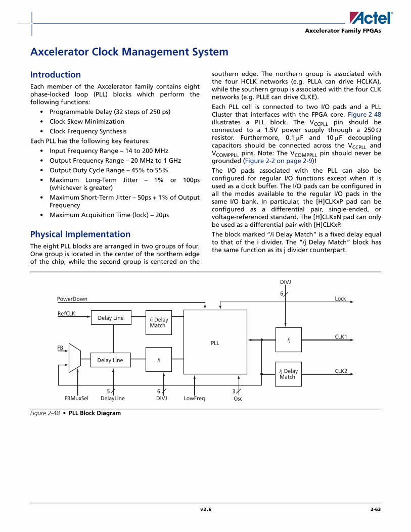
Axcelerator Family FPGAs
v2.6 2-63
Axcelerator Clock Management System
IntroductionEach member of the Axcelerator family contains eightphase-locked loop (PLL) blocks which perform thefollowing functions:
• Programmable Delay (32 steps of 250 ps)
• Clock Skew Minimization
• Clock Frequency Synthesis
Each PLL has the following key features:
• Input Frequency Range – 14 to 200 MHz
• Output Frequency Range – 20 MHz to 1 GHz
• Output Duty Cycle Range – 45% to 55%
• Maximum Long-Term Jitter – 1% or 100ps(whichever is greater)
• Maximum Short-Term Jitter – 50ps + 1% of OutputFrequency
• Maximum Acquisition Time (lock) – 20µs
Physical ImplementationThe eight PLL blocks are arranged in two groups of four.One group is located in the center of the northern edgeof the chip, while the second group is centered on the
southern edge. The northern group is associated withthe four HCLK networks (e.g. PLLA can drive HCLKA),while the southern group is associated with the four CLKnetworks (e.g. PLLE can drive CLKE).
Each PLL cell is connected to two I/O pads and a PLLCluster that interfaces with the FPGA core. Figure 2-48illustrates a PLL block. The VCCPLL pin should beconnected to a 1.5V power supply through a 250 Ωresistor. Furthermore, 0.1 µF and 10 µF decouplingcapacitors should be connected across the VCCPLL andVCOMPPLL pins. Note: The VCOMPPLL pin should never begrounded (Figure 2-2 on page 2-9)!
The I/O pads associated with the PLL can also beconfigured for regular I/O functions except when it isused as a clock buffer. The I/O pads can be configured inall the modes available to the regular I/O pads in thesame I/O bank. In particular, the [H]CLKxP pad can beconfigured as a differential pair, single-ended, orvoltage-referenced standard. The [H]CLKxN pad can onlybe used as a differential pair with [H]CLKxP.
The block marked “/i Delay Match” is a fixed delay equalto that of the i divider. The “/j Delay Match” block hasthe same function as its j divider counterpart.
Figure 2-48 • PLL Block Diagram
RefCLK
FB
Lock6
DIVJ
CLK1
CLK2
FBMuxSel DelayLine DIVJ LowFreq Osc5 6 3
Delay Line
PowerDown
Delay Line
PLL
/i Delay Match
/j Delay Match
/i
/j

Axcelerator Family FPGAs
2-64 v2.6
Functional DescriptionFigure 2-48 on page 2-63 illustrates a block diagram ofthe PLL. The PLL contains two dividers, i and j, that allowfrequency scaling of the clock signal:
• The i divider in the feedback path allowsmultiplication of the input clock by integer factorsranging from 1 to 64, and the resultant frequencyis available at the output of the PLL block.
• The j divider divides the PLL output by integerfactors ranging from 1 to 64, and the divided clockis available at CLK1.
• The two dividers together can implement anycombination of multiplication and division up to amaximum frequency of 1 GHz on CLK1. Both theCLK1 and CLK2 outputs have a fixed 50/50 dutycycle.
• The output frequencies of the two clocks are givenby the following formulas (fREF is the referenceclock frequency):
fCLK1 = fREF * (DividerI) / (DividerJ)
EQ 2-4
fCLK2 = fREF * (DividerI)
EQ 2-5
• CLK2 provides the PLL output directly—withoutdivision
The input and output frequency ranges are selected byLowFreq and Osc(2:0), respectively. These functions andtheir possible values are detailed in Table 2-79.
The delay lines shown in Figure 2-48 on page 2-63 areprogrammable. The feedback clock path can be delayed(using the five DelayLine bits) relative to the referenceclock (or vice versa) by up to 3.75 ns in increments of250 ps. Table 2-79 describes the usage of these bits. Thedelay increments are independent of frequency, so thisresults in phase changes that vary with frequency. Thedelay value is highly dependent on VCC and the speedgrade.
Figure 2-49 on page 2-65 is a logical diagram of thevarious control signals to the PLL and shows how the PLLinterfaces with the global and routing networks of theFPGA. Note that not all signals are user-accessible. Thesenon-user-accessible signals are used by Actel's place-and-route tool to control the configuration of the PLL. Theuser gains access to these control signals either basedupon the connections built in the user's design orthrough the special macros (Table 2-83 on page 2-67)inserted into the design. For example, connecting themacro PLLOUT to CLK2 will control the OUTSEL signal.
Table 2-79 • PLL Interface Signals
Signal Name Type User Accessible Allowable Values Function
RefCLK Input Yes Reference Clock for the PLL
FB Input Yes Feedback port for the PLL
PowerDown Input Yes PLL power down control
0 PLL powered down
1 PLL active
DIVI[5:0] Input Yes 1 to 64, in unsigned binary notation offset
by -1
Sets value for feedback divider (multiplier)
DIVJ[5:0] Input Yes Sets value for CLK1 divider
LowFreq Input Yes Input frequency range selector
0 50–200 MHz
1 14–50 MHz
Osc[2:0] Input Yes Output frequency range selector
XX0 400–1000 MHZ
001 200–400 MHZ
011 100–200 MHZ
101 50–100 MHZ
111 20–50 MHZ
DelayLine[4:0] Input Yes –15 to +15 (increments), in signed-and-magnitude binary
representation
Clock Delay (positive/negative) in increments of 250 ps, withmaximum value of ± 3.75 ns
FBMuxSel Input No Selects the source for the feedback input
REFSEL Input No Selects the source for the reference clock
OUTSEL Input No Selects the source for the routed net output
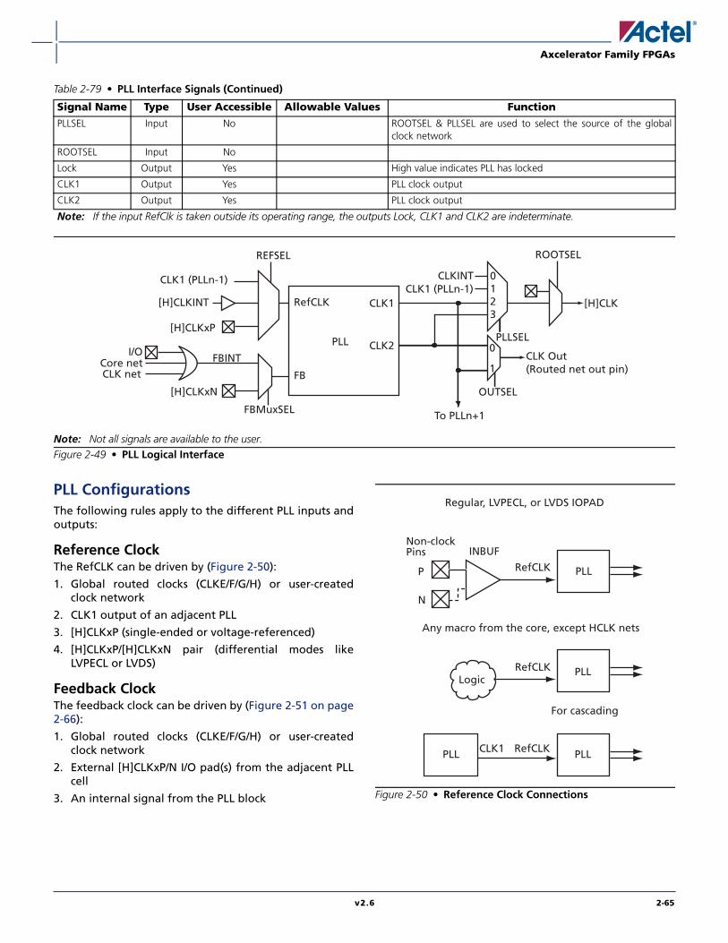
Axcelerator Family FPGAs
v2.6 2-65
PLL Configurations The following rules apply to the different PLL inputs andoutputs:
Reference ClockThe RefCLK can be driven by (Figure 2-50):
1. Global routed clocks (CLKE/F/G/H) or user-createdclock network
2. CLK1 output of an adjacent PLL
3. [H]CLKxP (single-ended or voltage-referenced)
4. [H]CLKxP/[H]CLKxN pair (differential modes likeLVPECL or LVDS)
Feedback ClockThe feedback clock can be driven by (Figure 2-51 on page2-66):
1. Global routed clocks (CLKE/F/G/H) or user-createdclock network
2. External [H]CLKxP/N I/O pad(s) from the adjacent PLLcell
3. An internal signal from the PLL block
PLLSEL Input No ROOTSEL & PLLSEL are used to select the source of the globalclock network
ROOTSEL Input No
Lock Output Yes High value indicates PLL has locked
CLK1 Output Yes PLL clock output
CLK2 Output Yes PLL clock output
Note: If the input RefClk is taken outside its operating range, the outputs Lock, CLK1 and CLK2 are indeterminate.
Note: Not all signals are available to the user.Figure 2-49 • PLL Logical Interface
Table 2-79 • PLL Interface Signals (Continued)
Signal Name Type User Accessible Allowable Values Function
RefCLK
FB
CLK1
CLK2
REFSEL ROOTSEL
FBMuxSEL
[H]CLKINT
[H]CLKxP
[H]CLKxN
I/OCore netCLK net
FBINT
0
0
1
123
CLKINTCLK1 (PLLn-1)CLK1 (PLLn-1)
[H]CLK
To PLLn+1
PLLSEL
OUTSEL
CLK Out(Routed net out pin)
PLL
Figure 2-50 • Reference Clock Connections
Non-clockPins
P
N
INBUF
PLLRefCLK
RefCLK PLL
RefCLK PLLPLL CLK1
Regular, LVPECL, or LVDS IOPAD
Any macro from the core, except HCLK nets
For cascading
Logic

Axcelerator Family FPGAs
2-66 v2.6
CLK1 and CLK2Both PLL outputs, CLK1 and CLK2, can be used to drive aglobal resource, an adjacent PLL RefCLK input, or a net inthe FPGA core. Not all drive combinations are possible(Table 2-80).
Restrictions on CLK1 and CLK2• When both are driving global resources, they must
be driving the same type of global resource (i.e.either HCLK or CLK).
• Only one can drive a routed net at any given time.
Table 2-81 and Table 2-82 specify all the possible CLK1and CLK2 connections for the north and south PLLs.HCLK1 and HCLK2 are used to denote the different HCLKnetworks when two are being driven at the same time bya single PLL (Note that HCLK1 is the primary clockresource associated with the PLL, and HCLK2 is the clockresource associated with the adjacent PLL). Likewise,CLK1 and CLK2 are used to denote the different CLKnetworks when two are being driven at the same time bya single PLL (Figure 2-48 on page 2-63).
Figure 2-51 • Feedback Clock Connections
Table 2-80 • PLL General Connections Rules
CLK1 CLK2
HCLK HCLK
CLK CLK
HCLK Routed net output
Routed net output HCLK
HCLK NONE
NONE HCLK
CLK NONE
NONE CLK
Note: The PLL outputs remain Low when REFCLK is constant(either Low or High).
PLLFB
FBPLL
PLLOUT/PLLRCLK
Any macro except HCLK macros
Table 2-81 • North PLL Connections
CLK1 CLK2
HCLK1 Routed net
HCLK1 Unused
HCLK2 HCLK1
HCLK2 Routed net
HCLK2 Both HCLK1 and routed net
HCLK2 Unused
Unused HCLK1
Unused Routed net
Unused Both HCLK1 and routed net
Unused Unused
Routed net HCLK1
Routed net Unused
Both HCLK1 and HCLK2 Routed net
Both HCLK1 and HCLK2 Unused
Both HCLK1 and routed net Unusable
Both HCLK2 and routed net HCLK1
Both HCLK2 and routed net Unused
HCLK1, HCLK2, and routed net Unusable
Note: Designer software currently does not support all of theseconnections. Only exclusive connections where oneoutput connects to a single net are supported at this time(e.g.CLK1 driving HCLK1, and HCLK2 is not supported).
Table 2-82 • South PLL Connections
CLK1 CLK2
CLK1 Routed net
CLK1 Unused
CLK2 CLK1
CLK2 Routed net
CLK2 Both CLK1 and routed net
CLK2 Unused
Unused CLK1
Unused Routed net
Unused Both CLK1 and routed net
Unused Unused
Routed net CLK1
Routed net Unused
Both CLK1 and CLK2 Routed net
Both CLK1 and CLK2 Unused
Both CLK1 and routed net Unusable
Both CLK2 and routed net CLK1
Both CLK2 and routed net Unused
CLK1, CLK2, and routed net Unusable
Note: Designer software currently does not support all of theseconnections. Only exclusive connections where oneoutput connects to a single net are supported at this time(e.g., CLK1 driving both CLK1 and CLK2 is not supported).

Axcelerator Family FPGAs
v2.6 2-67
Special PLL MacrosTable 2-83 shows the macros used to connect the RefCLK input and CLK1 and CLK2 outputs using the different routingresources.
Table 2-83 • PLL Special Macros
Macro Name Usage
PLLINT Connects RefCLK to a regular routed net or a pad.
PLLRCLK Connects CLK1 or CLK2 to the CLK network.
PLLHCLK Connects CLK1 or CLK2 to the HCLK network.
PLLOUT Connects CLK1 or CLK2 to a regular routed net.
Table 2-84 • Electrical Specifications
Parameter Value Notes
Frequency Ranges
Reference Frequency (min.) 14 MHz Lowest input frequency
Reference Frequency (max.) 200 MHz Highest input frequency
OSC Frequency (min.) 20 MHz Lowest output frequency
OSC Frequency (max.) 1 GHz Highest output frequency
Jitter
Long-Term Jitter (max.) 1% Percentage of period, low reference clock frequencies
Long-Term Jitter (max.) 100ps High reference clock frequencies
Short-Term Jitter (max.) 50ps+1% Percentage of output frequency
Acquisition Time (lock) from Cold Start
Acquisition Time (max.)* 400 cycles Period of low reference clock frequencies
Acquisition Time (max.)* 1.5 µs High reference clock frequencies
Power Consumption
Analog Supply Current (low freq.) 200µA Current at minimum oscillator frequency
Analog Supply Current (high freq.) 200µA Frequency-dependent current
Digital Supply Current (low freq.) 0.5µA/MHz Current at maximum oscillator frequency, unloaded
Digital Supply Current (high freq.) 1µA/MHz Frequency-dependent current
Duty Cycle
Minimum Output Duty Cycle 45%
Maximum Output Duty Cycle 55%
Note: *The lock bit remains Low until RefCLK reaches the minimum input frequency.
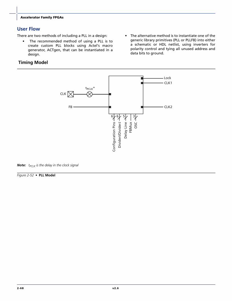
Axcelerator Family FPGAs
2-68 v2.6
User FlowThere are two methods of including a PLL in a design:
• The recommended method of using a PLL is tocreate custom PLL blocks using Actel's macrogenerator, ACTgen, that can be instantiated in adesign.
• The alternative method is to instantiate one of thegeneric library primitives (PLL or PLLFB) into eithera schematic or HDL netlist, using inverters forpolarity control and tying all unused address anddata bits to ground.
Timing Model
Note: tPCLK is the delay in the clock signal
Figure 2-52 • PLL Model
CLK
CLK1Lock
CLK2
Co
nfi
gu
rati
on
Pin
s
Div
ider
I/Div
ider
J
Del
ay L
ine
FBM
ux
OSC
6 356
FB
tPCLK*

Axcelerator Family FPGAs
v2.6 2-69
Sample Implementations
Frequency SynthesisFigure 2-53 illustrates an example where the PLL is usedto multiply a 155.5 MHz external clock up to 622 MHz.Note that the same PLL schematic could use an external350 MHz clock, which is divided down to 155 MHz by theFPGA internal logic.
Figure 2-54 illustrates the PLL using both dividers tosynthesize a 133 MHz output clock from a 155 MHz inputreference clock. The input frequency of 155 MHz ismultiplied by 6 and divided by 7, giving a CLK1 outputfrequency of 132.86 MHz. When dividers are used, agiven ratio can be generated in multiple ways, allowingthe user to stay within the operating frequency ranges ofthe PLL.
Figure 2-53 • Using the PLL 155.5 MHz In, 622 MHz Out
Figure 2-54 • Using the PLL 155 MHz In, 133 MHz Out
Delay Line
PLL
Delay Line
RefCLK
FB
/i
6
/j
6
CLK1
PowerDown
Lock
CLK2
FBMuxSel5
DividerIDelayLine
DividerJ
LowFreq3Osc
÷4
155.5 MHz
622 MHz
/i Delay Match
/j Delay Match
5
Delay Line
PLL
Delay Line
RefCLK
FB
/i
6
/j
6
CLK1
PowerDownLock
CLK2
FBMuxSel DividerIDelayLine
DividerJ
LowFreq
3
Osc
÷6
155 MHz 132.8 MHz155 MHz
155 MHz
930 MHz
/7
Yes
/i Delay Match
/j Delay Match

Axcelerator Family FPGAs
2-70 v2.6
Adjustable Clock DelayFigure 2-55 illustrates using the PLL to delay the reference clock by employing one of the adjustable delay lines. In thiscase, the output clock is delayed relative to the reference clock. Delaying the reference clock relative to the outputclock is accomplished by using the delay line in the feedback path.
Figure 2-55 • Using the PLL Delaying the Reference Clock
Delay Line
Delay Line
PLL
RefCLK
FB
6
/j
6
CLK1
PowerDownLock
CLK2
FBMuxSel
5
DividerIDelayLine
DividerJ
LowFreq
3
Osc
÷1
133 MHz
133 MHz
/j
/i Delay Match
/j Delay Match
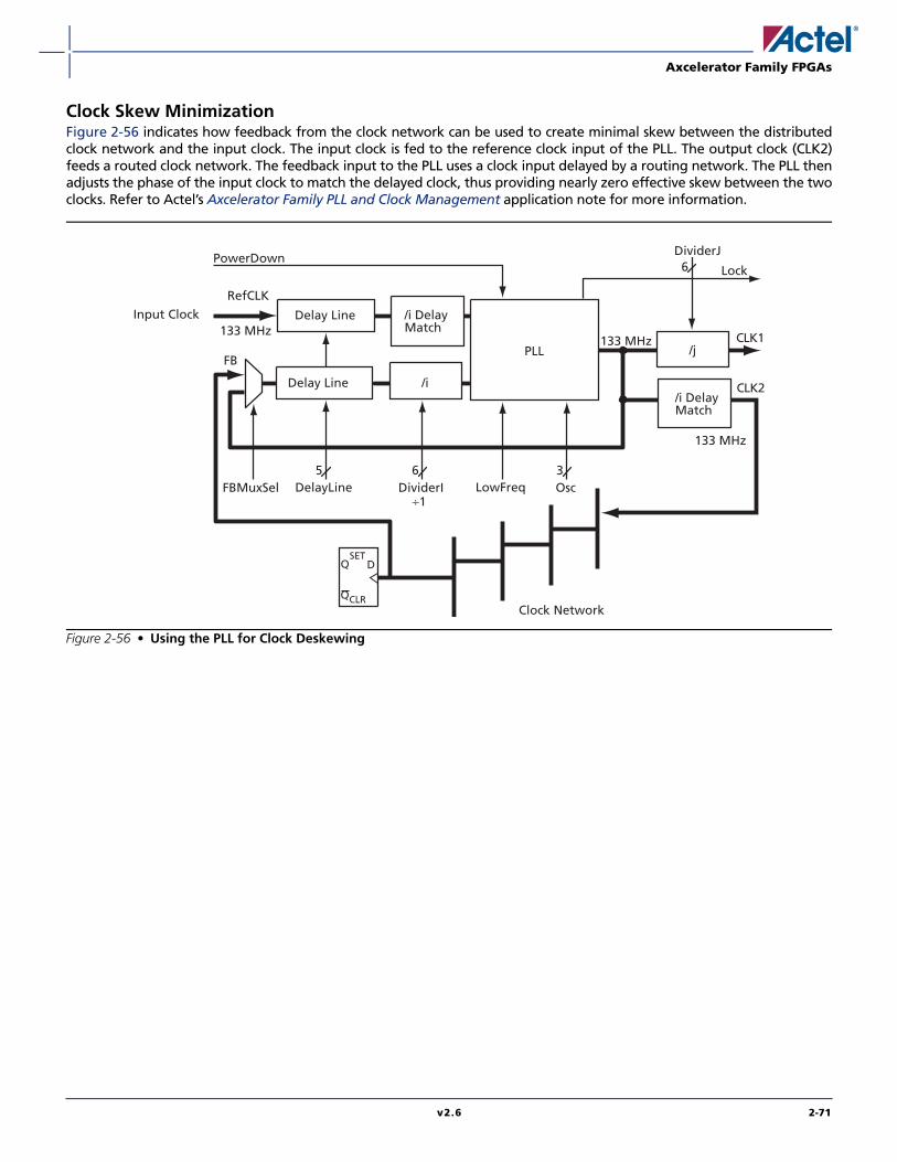
Axcelerator Family FPGAs
v2.6 2-71
Clock Skew MinimizationFigure 2-56 indicates how feedback from the clock network can be used to create minimal skew between the distributedclock network and the input clock. The input clock is fed to the reference clock input of the PLL. The output clock (CLK2)feeds a routed clock network. The feedback input to the PLL uses a clock input delayed by a routing network. The PLL thenadjusts the phase of the input clock to match the delayed clock, thus providing nearly zero effective skew between the twoclocks. Refer to Actel’s Axcelerator Family PLL and Clock Management application note for more information.
Figure 2-56 • Using the PLL for Clock Deskewing
QCLR
Delay Line
PLL
RefCLK
FB
6
/j
6
CLK1
PowerDown
Input Clock
Clock Network
Lock
CLK2
FBMuxSel5
DividerIDelayLine
DividerJ
LowFreq3Osc
÷1
133 MHz
133 MHz
DQSET
133 MHz
Delay Line /i
/i Delay Match
/i Delay Match
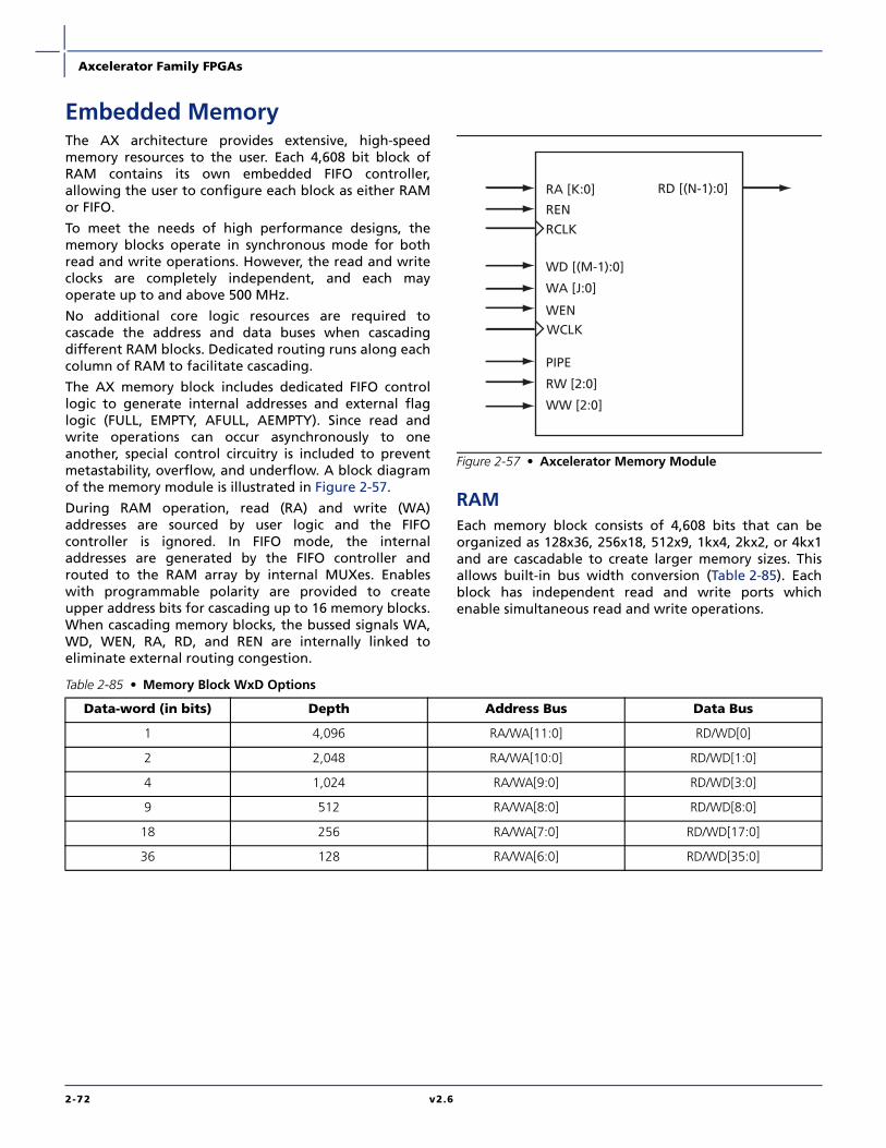
Axcelerator Family FPGAs
2-72 v2.6
Embedded MemoryThe AX architecture provides extensive, high-speedmemory resources to the user. Each 4,608 bit block ofRAM contains its own embedded FIFO controller,allowing the user to configure each block as either RAMor FIFO.
To meet the needs of high performance designs, thememory blocks operate in synchronous mode for bothread and write operations. However, the read and writeclocks are completely independent, and each mayoperate up to and above 500 MHz.
No additional core logic resources are required tocascade the address and data buses when cascadingdifferent RAM blocks. Dedicated routing runs along eachcolumn of RAM to facilitate cascading.
The AX memory block includes dedicated FIFO controllogic to generate internal addresses and external flaglogic (FULL, EMPTY, AFULL, AEMPTY). Since read andwrite operations can occur asynchronously to oneanother, special control circuitry is included to preventmetastability, overflow, and underflow. A block diagramof the memory module is illustrated in Figure 2-57.
During RAM operation, read (RA) and write (WA)addresses are sourced by user logic and the FIFOcontroller is ignored. In FIFO mode, the internaladdresses are generated by the FIFO controller androuted to the RAM array by internal MUXes. Enableswith programmable polarity are provided to createupper address bits for cascading up to 16 memory blocks.When cascading memory blocks, the bussed signals WA,WD, WEN, RA, RD, and REN are internally linked toeliminate external routing congestion.
RAMEach memory block consists of 4,608 bits that can beorganized as 128x36, 256x18, 512x9, 1kx4, 2kx2, or 4kx1and are cascadable to create larger memory sizes. Thisallows built-in bus width conversion (Table 2-85). Eachblock has independent read and write ports whichenable simultaneous read and write operations.
Figure 2-57 • Axcelerator Memory Module
RA [K:0] RD [(N-1):0]
REN
RCLK
WD [(M-1):0]
WA [J:0]
WENWCLK
PIPE
RW [2:0]
WW [2:0]
Table 2-85 • Memory Block WxD Options
Data-word (in bits) Depth Address Bus Data Bus
1 4,096 RA/WA[11:0] RD/WD[0]
2 2,048 RA/WA[10:0] RD/WD[1:0]
4 1,024 RA/WA[9:0] RD/WD[3:0]
9 512 RA/WA[8:0] RD/WD[8:0]
18 256 RA/WA[7:0] RD/WD[17:0]
36 128 RA/WA[6:0] RD/WD[35:0]

Axcelerator Family FPGAs
v2.6 2-73
ClocksThe RCLK and the WCLK have independent sourcepolarity selection and can be sourced by any global orlocal signal.
RAM ConfigurationsThe AX architecture allows the read side and write sideof RAMs to be organized independently, allowing forbus conversion. For example, the write side can be set to256x18 and the read side to 512x9.
Both the write width and read width for the RAM blockscan be specified independently and changed dynamicallywith the WW (write width) and RW (read width) pins.
The D x W different configurations are: 128 x 36,256 x 18, 512 x 9, 1k x 4, 2k x 2, and 4k x 1. The allowableRW and WW values are shown in Table 2-87.
When widths of one, two, and four are selected, theninth bit is unused. For example, when writing nine-bitvalues and reading four-bit values, only the first four bitsand the second four bits of each nine-bit value areaddressable for read operations. The ninth bit is notaccessible. Conversely, when writing four-bit values andreading nine-bit values, the ninth bit of a read operationwill be undefined.
Note that the RAM blocks employ little-endian byteorder for read and write operations.
Table 2-86 • RAM Signal Description
Signal Direction Description
WCLK Input Write clock (can be active on either edge).
WA[J:0] Input Write address bus.The value J is dependent on the RAM configuration and the number of cascadedmemory blocks. The valid range for J is from 6 to15.
WD[M-1:0] Input Write data bus. The value M is dependent on the RAM configuration and can be 1, 2, 4, 9, 18, or36.
RCLK Input Read clock (can be active on either edge).
RA[K:0] Input Read address bus. The value K is dependent on the RAM configuration and the number of cascadedmemory blocks. The valid range for K is from 6 to 15.
RD[N-1:0] Output Read data bus. The value N is dependent on the RAM configuration and can be 1, 2, 4, 9, 18, or 36.
REN Input Read enable. When this signal is valid on the active edge of the clock, data at location RA will bedriven onto RD.
WEN Input Write enable. When this signal is valid on the active edge of the clock, WD data will be written atlocation WA.
RW[2:0] Input Width of the read operation dataword.
WW[2:0] Input Width of the write operation dataword.
Pipe Input Sets the pipe option to be on or off.
Table 2-87 • Allowable RW and WW Values
RW(2:0) WW(2:0) D x W
000 000 4k x 1
001 001 2k x 2
010 010 1k x 4
011 011 512 x 9
100 100 256 x 18
101 101 128 x 36
11x 11x reserved

Axcelerator Family FPGAs
2-74 v2.6
Modes of OperationThere are two read modes and one write mode:
• Read Nonpipelined (synchronous – one clock edge)
• Read Pipelined (synchronous – two clock edges)
• Write (synchronous – one clock edge)
In the standard read mode, new data is driven onto theRD bus in the clock cycle immediately following RA andREN valid. The read address is registered on the read-port active-clock edge and data appears at read-dataafter the RAM access time. Setting the PIPE to OFFenables this mode.
The pipelined mode incurs an additional clock delayfrom address to data, but enables operation at a much
higher frequency. The read-address is registered on theread-port active-clock edge, and the read data isregistered and appears at RD after the second read clockedge. Setting the PIPE to ON enables this mode.
On the write active-clock edge, the write data arewritten into the SRAM at the write address when WEN ishigh. The setup time of the write address, write enables,and write data are minimal with respect to the writeclock.
Write and read transfers are described with timingrequirements beginning in "Timing Characteristics".
Timing Characteristics
Figure 2-58 • SRAM Model
Figure 2-59 • RAM Write Timing Waveforms
WD RD
RA
REN
WA
WCLK RCLK
WEN
WCLK
tWCKP
tWxxSU tWxxHD
tWCKH tWCKL
WA<11:0>, WD<35:0>, WEN<4:0>

Axcelerator Family FPGAs
v2.6 2-75
Figure 2-60 • RAM Read Timing Waveforms
Table 2-88 • One RAM BlockWorst-Case Commercial Conditions VCCA = 1.425V, VCCI = 3.0V, TJ = 70°C
'–2' Speed '–1' Speed 'Std' Speed
Parameter Description Min. Max. Min. Max. Min. Max. Units
Write Mode
tWDASU Write Data Setup vs. WCLK 1.08 1.23 1.45 ns
tWDAHD Write Data Hold vs. WCLK 0.22 0.25 0.30 ns
tWADSU Write Address Setup vs. WCLK 1.08 1.23 1.45 ns
tWADHD Write Address Hold vs. WCLK 0.22 0.25 0.30 ns
tWENSU Write Enable Setup vs. WCLK 1.08 1.23 1.45 ns
tWENHD Write Enable Hold vs. WCLK 0.22 0.25 0.30 ns
tWCKH WCLK Minimum High Pulse Width 0.98 1.11 1.31 ns
tWCLK WCLK Minimum Low Pulse Width 1.15 1.30 1.53 ns
tWCKP WCLK Minimum Period 2.29 2.61 3.07 ns
Read Mode
tRADSU Read Address Setup vs. RCLK 0.81 0.92 1.08 ns
tRADHD Read Address Hold vs. RCLK 0.00 0.00 0.00 ns
tRENSU Read Enable Setup vs. RCLK 0.81 0.92 1.08 ns
tRENHD Read Enable Hold vs. RCLK 0.00 0.00 0.00 ns
tRCK2RD1 RCLK-To-OUT (Pipelined) 1.39 1.59 1.86 ns
tRCK2RD2 RCLK-To-OUT (Non-Pipelined) 2.62 2.98 3.5 ns
tRCLKH RCLK Minimum High Pulse Width 1.00 1.14 1.34 ns
tRCLKL RCLK Minimum Low Pulse Width 1.21 1.38 1.62 ns
tRCKP RCLK Minimum Period 2.42 2.76 3.24 ns
RCLK
RA<11:0>, REN<4:0>
RD <35:0>
tRxxSU tRxxHD
tRCKP tRCKH tRCKL
tRCK2RD1 tRCK2RD2

Axcelerator Family FPGAs
2-76 v2.6
Table 2-89 • Two RAM Blocks CascadedWorst-Case Commercial Conditions VCCA = 1.425V, VCCI = 3.0V, TJ = 70°C
'–2' Speed '–1' Speed 'Std' Speed
Parameter Description Min. Max. Min. Max. Min. Max. Units
Write Mode
tWDASU Write Data Setup vs. WCLK 1.39 1.59 1.86 ns
tWDAHD Write Data Hold vs. WCLK 0.22 0.25 0.3 ns
tWADSU Write Address Setup vs. WCLK 1.39 1.59 1.86 ns
tWADHD Write Address Hold vs. WCLK 0.22 0.25 0.3 ns
tWENSU Write Enable Setup vs. WCLK 1.39 1.59 1.86 ns
tWENHD Write Enable Hold vs. WCLK 0.22 0.25 0.3 ns
tWCKH WCLK Minimum High Pulse Width 0.98 1.11 1.31 ns
tWCLK WCLK Minimum Low Pulse Width 2.29 2.61 3.07 ns
tWCKP WCLK Minimum Period 4.58 5.22 6.13 ns
Read Mode
tRADSU Read Address Setup vs. RCLK 1.7 1.94 2.28 ns
tRADHD Read Address Hold vs. RCLK 0.00 0.00 0.00 ns
tRENSU Read Enable Setup vs. RCLK 1.7 1.94 2.28 ns
tRENHD Read Enable Hold vs. RCLK 0.00 0.00 0.00 ns
tRCK2RD1 RCLK-To-OUT (Pipelined) 1.51 1.72 2.02 ns
tRCK2RD2 RCLK-To-OUT (Non-Pipelined) 2.76 3.14 3.69 ns
tRCLKH RCLK Minimum High Pulse Width 0.95 1.08 1.27 ns
tRCLKL RCLK Minimum Low Pulse Width 2.46 2.8 3.29 ns
tRCKP RCLK Minimum Period 4.92 5.6 6.59 ns
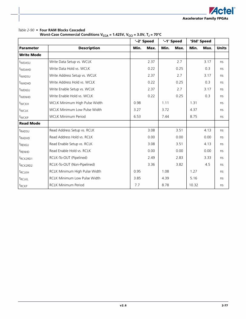
Axcelerator Family FPGAs
v2.6 2-77
Table 2-90 • Four RAM Blocks CascadedWorst-Case Commercial Conditions VCCA = 1.425V, VCCI = 3.0V, TJ = 70°C
'–2' Speed '–1' Speed 'Std' Speed
Parameter Description Min. Max. Min. Max. Min. Max. Units
Write Mode
tWDASU Write Data Setup vs. WCLK 2.37 2.7 3.17 ns
tWDAHD Write Data Hold vs. WCLK 0.22 0.25 0.3 ns
tWADSU Write Address Setup vs. WCLK 2.37 2.7 3.17 ns
tWADHD Write Address Hold vs. WCLK 0.22 0.25 0.3 ns
tWENSU Write Enable Setup vs. WCLK 2.37 2.7 3.17 ns
tWENHD Write Enable Hold vs. WCLK 0.22 0.25 0.3 ns
tWCKH WCLK Minimum High Pulse Width 0.98 1.11 1.31 ns
tWCLK WCLK Minimum Low Pulse Width 3.27 3.72 4.37 ns
tWCKP WCLK Minimum Period 6.53 7.44 8.75 ns
Read Mode
tRADSU Read Address Setup vs. RCLK 3.08 3.51 4.13 ns
tRADHD Read Address Hold vs. RCLK 0.00 0.00 0.00 ns
tRENSU Read Enable Setup vs. RCLK 3.08 3.51 4.13 ns
tRENHD Read Enable Hold vs. RCLK 0.00 0.00 0.00 ns
tRCK2RD1 RCLK-To-OUT (Pipelined) 2.49 2.83 3.33 ns
tRCK2RD2 RCLK-To-OUT (Non-Pipelined) 3.36 3.82 4.5 ns
tRCLKH RCLK Minimum High Pulse Width 0.95 1.08 1.27 ns
tRCLKL RCLK Minimum Low Pulse Width 3.85 4.39 5.16 ns
tRCKP RCLK Minimum Period 7.7 8.78 10.32 ns

Axcelerator Family FPGAs
2-78 v2.6
Table 2-91 • Eight RAM Blocks CascadedWorst-Case Commercial Conditions VCCA = 1.425V, VCCI = 3.0V, TJ = 70°C
'–2' Speed '–1' Speed 'Std' Speed
Parameter Description Min. Max. Min. Max. Min. Max. Units
Write Mode
tWDASU Write Data Setup vs. WCLK 5.78 6.58 7.74 ns
tWDAHD Write Data Hold vs. WCLK 0.22 0.25 0.3 ns
tWADSU Write Address Setup vs. WCLK 5.78 6.58 7.74 ns
tWADHD Write Address Hold vs. WCLK 0.22 0.25 0.3 ns
tWENSU Write Enable Setup vs. WCLK 5.78 6.58 7.74 ns
tWENHD Write Enable Hold vs. WCLK 0.22 0.25 0.3 ns
tWCKH WCLK Minimum High Pulse Width 0.98 1.11 1.31 ns
tWCLK WCLK Minimum Low Pulse Width 6.68 7.6 8.94 ns
tWCKP WCLK Minimum Period 13.35 15.21 17.88 ns
Read Mode
tRADSU Read Address Setup vs. RCLK 6.75 7.69 9.04 ns
tRADHD Read Address Hold vs. RCLK 0.00 0.00 0.00 ns
tRENSU Read Enable Setup vs. RCLK 6.75 7.69 9.04 ns
tRENHD Read Enable Hold vs. RCLK 0.00 0.00 0.00 ns
tRCK2RD1 RCLK-To-OUT (Pipelined) 3.57 4.06 4.77 ns
tRCK2RD2 RCLK-To-OUT (Non-Pipelined) 5.48 6.24 7.34 ns
tRCLKH RCLK Minimum High Pulse Width 0.95 1.08 1.27 ns
tRCLKL RCLK Minimum Low Pulse Width 7.51 8.55 10.05 ns
tRCKP RCLK Minimum Period 15.02 17.11 20.11 ns
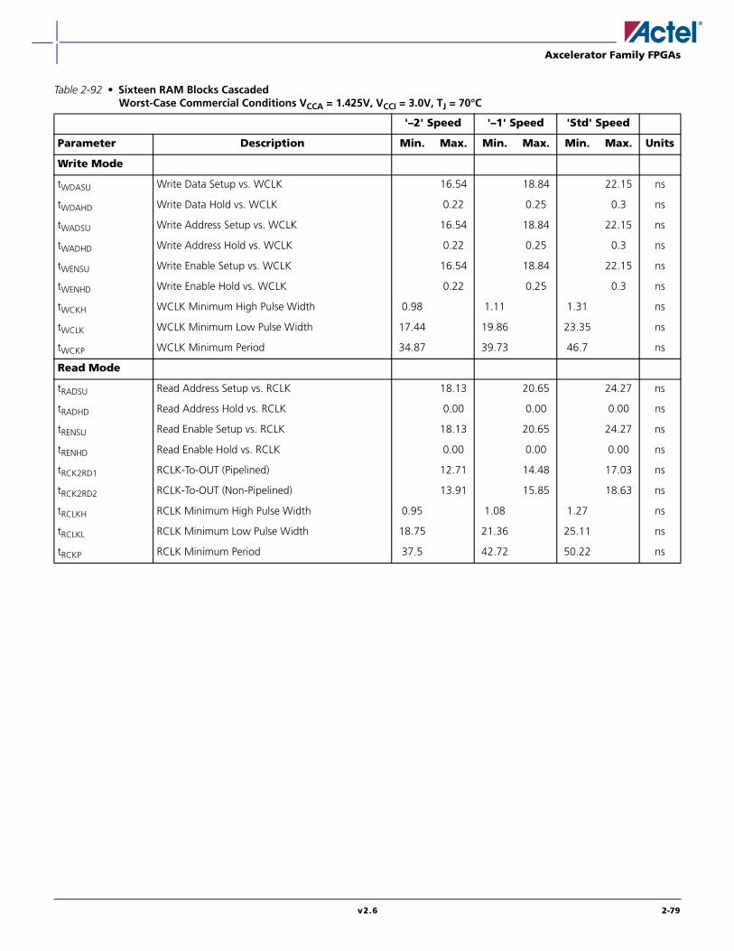
Axcelerator Family FPGAs
v2.6 2-79
Table 2-92 • Sixteen RAM Blocks CascadedWorst-Case Commercial Conditions VCCA = 1.425V, VCCI = 3.0V, TJ = 70°C
'–2' Speed '–1' Speed 'Std' Speed
Parameter Description Min. Max. Min. Max. Min. Max. Units
Write Mode
tWDASU Write Data Setup vs. WCLK 16.54 18.84 22.15 ns
tWDAHD Write Data Hold vs. WCLK 0.22 0.25 0.3 ns
tWADSU Write Address Setup vs. WCLK 16.54 18.84 22.15 ns
tWADHD Write Address Hold vs. WCLK 0.22 0.25 0.3 ns
tWENSU Write Enable Setup vs. WCLK 16.54 18.84 22.15 ns
tWENHD Write Enable Hold vs. WCLK 0.22 0.25 0.3 ns
tWCKH WCLK Minimum High Pulse Width 0.98 1.11 1.31 ns
tWCLK WCLK Minimum Low Pulse Width 17.44 19.86 23.35 ns
tWCKP WCLK Minimum Period 34.87 39.73 46.7 ns
Read Mode
tRADSU Read Address Setup vs. RCLK 18.13 20.65 24.27 ns
tRADHD Read Address Hold vs. RCLK 0.00 0.00 0.00 ns
tRENSU Read Enable Setup vs. RCLK 18.13 20.65 24.27 ns
tRENHD Read Enable Hold vs. RCLK 0.00 0.00 0.00 ns
tRCK2RD1 RCLK-To-OUT (Pipelined) 12.71 14.48 17.03 ns
tRCK2RD2 RCLK-To-OUT (Non-Pipelined) 13.91 15.85 18.63 ns
tRCLKH RCLK Minimum High Pulse Width 0.95 1.08 1.27 ns
tRCLKL RCLK Minimum Low Pulse Width 18.75 21.36 25.11 ns
tRCKP RCLK Minimum Period 37.5 42.72 50.22 ns

Axcelerator Family FPGAs
2-80 v2.6
FIFOEvery memory block has its own embedded FIFOcontroller. Each FIFO block has one read port and onewrite port. This embedded FIFO controller uses nointernal FPGA logic and features:
• Glitch-free FIFO Flags
• Gray-code address counters/pointers to preventmetastability problems
• Overflow and underflow control
Both ports are configurable in various sizes from 4k x 1to 128 x 36, similar to the RAM block size. Each port isfully synchronous.
Read and write operations can be completelyindependent. Data on the appropriate WD pins arewritten to the FIFO on every active WCLK edge as long asWEN is high. Data is read from the FIFO and output onthe appropriate RD pins on every active RCLK edge aslong as REN is asserted.
The FIFO block offers programmable almost-empty(AEMPTY) and almost-full (AFULL) flags as well as EMPTYand FULL flags (Figure 2-61):
• The FULL flag is synchronous to WCLK. It allowsthe FIFO to inhibit writing when full.
• The EMPTY flag is synchronous to RCLK. It allowsthe FIFO to inhibit reading at the empty condition.
Gray code counters are used to prevent metastabilityproblems associated with flag logic. The depth of theFIFO is dependent on the data width and the number ofmemory blocks used to create the FIFO. The writeoperations to the FIFO are synchronous with respect tothe WCLK, and the read operations are synchronous withrespect to the RCLK.
The FIFO block may be reset to the empty state.
Figure 2-61 • Axcelerator RAM with Embedded FIFO Controller
CNT 16E
CNT 16E =
=
AFVAL
AEVAL
>
> =
SUB
16
RCLK
WD
WCLK
CLR
FWEN
FREN
DEPTH[3:0]
RD [n-1:0]WD [n-1:0]
RCLK
WCLK
RA [J:0]
WA [J:0]
RENWEN
FULL
AEMPTY
AFULL
EMPTY
RD
PIPE
RW
[2:0
]W
W[2
:0]
WID
TH[2
:0]
RAM

Axcelerator Family FPGAs
v2.6 2-81
FIFO Flag LogicThe FIFO is user configurable into various DEPTHs andWIDTHs. Figure 2-62 shows the FIFO address counterdetails.
• Bits 11 to 5 are active for all modes.
• As the data word size is reduced, more least-significant bits are added to the address.
• As the number of cascaded blocks increases, thenumber of significant bits in the address increases.
For example, if four blocks are cascaded as a 1kx16 FIFOwith each block having a 1kx4 aspect ratio, bits 11 to 2 ofthe address will be used to specify locations within each
RAM block, whereas bits 13 and 12 will be used to specifythe RAM block.
The AFULL and AEMPTY flag threshold values areprogrammable. The threshold values are AFVAL andAEVAL, respectively. Although the trigger threshold foreach flag is defined with eight bits, the effective numberof threshold bits in the comparison depends on theconfiguration. The effective number of threshold bitscorresponds to the range of active bits in the FIFOaddress space (Table 2-93).
Note: Inactive counter bits are set to zero.Figure 2-62 • FIFO Address Counters
Table 2-93 • FIFO Flag Logic
Mode Inactive AEVAL/AFVAL bits Inactive DIFF bits (set to 0) DIFF comparison to AFVAL/AEVAL
Non-cascade [7:4] [15:12] DIFF[11:8] withAE/FVAL[3:0]
Cascade 2 blocks [7:5] [15:13] DIFF[12:8] withAE/FVAL[4:0]
Cascade 4 blocks [7:6] [15:14] DIFF[13:8] withAE/FVAL[5:0]
Cascade 8 blocks [7] [15] DIFF[14:8] withAE/FVAL[6:0]
Cascade 16 blocks None None DIFF[15:8] withAE/FVAL[7:0]
CNTR [12]activate
FIFO Address Counters
>> REN [4:0], RAD [11:0]>> WEN [4:0], WAD [11:0]
[12:W] [13:W][14:W]
[15:W]
128x36 1kx4512x9256x18
[11:5][11:4]
[11:3]
[11:2][11:1]
[11:0]
4kx12kx2
Variable Active Address Space
CNTR [15]activate
CNTR [2]activate
CNTR [3]activate
CNTR [4]activate
CNTR [11:5]always active
CNTR [13]activate
CNTR [14]activate
CNTR [0]activate
CNTR [1]activate
Cas 16 blks
by 1
by 2
by 4
by 9
by 18
by 36
Cas 2 blks
Cas 4 blks
Cas 8 blks
Mode when Active
Counter Bits
R/W EN[3]
R/W ADD[0]
R/W ADD[1]
R/W ADD[2]
R/W ADD[3]
R/W ADD[7:5]
R/W ADD[11:8]
R/W EN[0]
R/W EN[1]
R/W EN[2]
R/W ADD[4]
FIFO Address
AEVAL/AFVAL[7]
not compared
not compared
not compared
not compared
not compared
not compared
AEVAL/AFVAL[3:0]
AEVAL/AFVAL[4]
AEVAL/AFVAL[5]
AEVAL/AFVAL[6]
CNTR [15:0]
Alignment of Threshold bits

Axcelerator Family FPGAs
2-82 v2.6
Figure 2-63 illustrates flag generation. The Verilog codes for the flags are:
assign AF = (DIFF[15:0] >=AFVAL[7:0],8'b00000000)?1:0;
assign AE = (AEVAL[7:0],8'b00000000>=DIFF[15:0])?1:0;
The number of DIFF-bits active depends on the configuration depth and width (Table 2-94).
Figure 2-63 • ALMOST-EMPTY and ALMOST-FULL Logic
Table 2-94 • Number of Available Configuration Bits
Number of Blocks Block DxW Number of AEVAL/AFVAL Bits
1 1x1 4
2 1x2 4
2 2x1 5
4 1x4 4
4 2x2 5
4 4x1 6
8 1x8 4
8 2x4 5
8 4x2 6
8 8x1 7
16 1x16 4
16 2x8 5
16 4x4 6
16 8x2 7
16 16x1 8
ALMOST EMPTY and ALMOST FULL Logic
WCNTR[15:0]WCLK
RCNTR[15:0]RCLK
16
16
X
Y
X
Y
AEMPTY
AFULL
X>=Y(16 bit)DIFF [15:0]
AEVAL [7:0], GND [7:0] (MSB....LSB)
AFVAL [7:0], GND [7:0] (MSB....LSB)
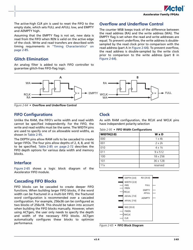
Axcelerator Family FPGAs
v2.6 2-83
The active-high CLR pin is used to reset the FIFO to theempty state, which sets FULL and AFULL low, and EMPTYand AEMPTY high.
Assuming that the EMPTY flag is not set, new data isread from the FIFO when REN is valid on the active edgeof the clock. Write and read transfers are described withtiming requirements in "Timing Characteristics" onpage 2-85.
Glitch EliminationAn analog filter is added to each FIFO controller toguarantee glitch-free FIFO-flag logic.
Overflow and Underflow ControlThe counter MSB keeps track of the difference betweenthe read address (RA) and the write address (WA). TheEMPTY flag is set when the read and write addresses areequal. To prevent underflow, the write address is double-sampled by the read clock prior to comparison with theread address (part A in Figure 2-64). To prevent overflow,the read address is double-sampled by the write clockprior to comparison to the write address (part B inFigure 2-64).
FIFO ConfigurationsUnlike the RAM, the FIFO's write width and read widthcannot be specified independently. For the FIFO, thewrite and read widths must be the same. The WIDTH pinsare used to specify one of six allowable word widths, asshown in Table 2-95.
The DEPTH pins allow RAM cells to be cascaded to createlarger FIFOs. The four pins allow depths of 2, 4, 8, and 16to be specified. Table 2-85 on page 2-72 describes theFIFO depth options for various data width and memoryblocks.
Interface Figure 2-65 shows a logic block diagram of theAxcelerator FIFO module.
Cascading FIFO BlocksFIFO blocks can be cascaded to create deeper FIFOfunctions. When building larger FIFO blocks, if the wordwidth can be fractured in a multi-bit FIFO, the fracturedword configuration is recommended over a cascadedconfiguration. For example, 256x36 can be configured astwo blocks of 256x18. This should be taken into accountwhen building the FIFO blocks manually. However, whenusing ACTgen, the user only needs to specify the depthand width of the necessary FIFO blocks. ACTgenautomatically configures these blocks to optimizeperformance.
Clock As with RAM configuration, the RCLK and WCLK pinshave independent polarity selection
Figure 2-64 • Overflow and Underflow Control
A B
= EMPTY
WA
RARCLK = FULL
RA
WAWCLK
Table 2-95 • FIFO Width Configurations
WIDTH(2:0) W x D
000 1 x 4k
001 2 x 2k
010 4 x 1k
011 9 x 512
100 18 x 256
101 36 x 128
11x reserved
Figure 2-65 • FIFO Block Diagram
DEPTH [3:0] RD [35:0]
FULL
EMPTYAFULL
AEMPTY
WIDTH [2:0]
FWEN
FRENPIPE
RCLK
WD [35:0]
AEVAL [7:0]
AFVAL [7:0]
WCLK
CLR
Axcelerator Family FPGAs
2-84 v2.6
Table 2-96 • FIFO Signal Description
Signal Direction Description
WCLK Input Write clock (active either edge).
FWEN Input FIFO write enable. When this signal is asserted, the WD bus data is latched into theFIFO, and the internal write counters are incremented.
WD[N-1:0] Input Write data bus. The value N is dependent on the RAM configuration and can be 1,2, 4, 9, 18, or 36.
FULL Output Active high signal indicating that the FIFO is FULL. When this signal is set,additional write requests are ignored.
AFULL Output Active high signal indicating that the FIFO is AFULL.
AFVAL Input 8-bit input defining the AFULL value of the FIFO.
RCLK Input Read clock (active either edge).
FREN Input FIFO read enable.
RD[N-1:0] Output Read data bus. The value N is dependent on the RAM configuration and can be 1,2, 4, 9, 18, or 36.
EMPTY Output Empty flag indicating that the FIFO is EMPTY. When this signal is asserted,attempts to read the FIFO will be ignored.
AEMPTY Output Active high signal indicating that the FIFO is AEMPTY.
AEVAL Input 8-bit input defining the almost-empty value of the FIFO.
PIPE Input Sets the pipe option on or off.
CLR Input Active high clear input.
DEPTH Input Determines the depth of the FIFO and the number of FIFOs to be cascaded.
WIDTH Input Determines the width of the dataword / width of the FIFO, and the number of theFIFOs to be cascaded.
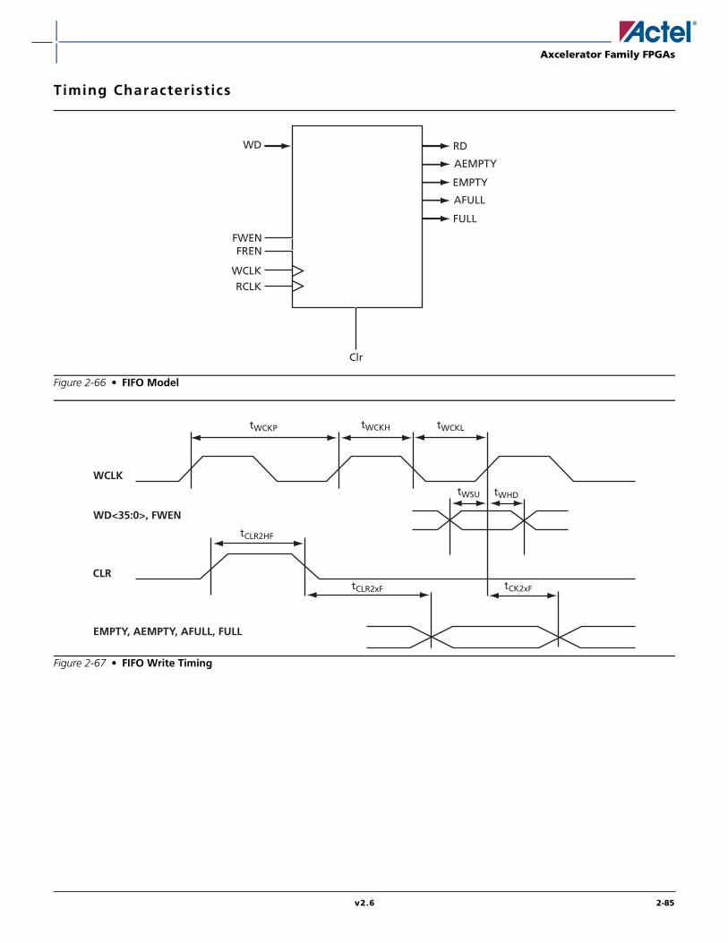
Axcelerator Family FPGAs
v2.6 2-85
Timing Characteristics
Figure 2-66 • FIFO Model
Figure 2-67 • FIFO Write Timing
WD
FWENFREN
RCLKWCLK
RD
AFULL
EMPTY
AEMPTY
FULL
Clr
tWCKP
tWSU tWHD
tCK2xFtCLR2xF
tCLR2HF
tWCKH tWCKL
WCLK
CLR
WD<35:0>, FWEN
EMPTY, AEMPTY, AFULL, FULL

Axcelerator Family FPGAs
2-86 v2.6
Figure 2-68 • FIFO Read Timing
Table 2-97 • One FIFO BlockWorst-Case Commercial Conditions VCCA = 1.425V, VCCI = 3.0V, TJ = 70°C
'–2' Speed '–1' Speed 'Std' Speed
Parameter Description Min. Max. Min. Max. Min. Max. Units
FIFO Module Timing
tWSU Write Setup 1.08 1.23 1.45 ns
tWHD Write Hold 0.22 0.25 0.30 ns
tWCKH WCLK High 0.98 1.11 1.31 ns
tWCKL WCLK Low 1.15 1.30 1.53 ns
tWCKP Minimum WCLK Period 2.3 2.6 3.06 ns
tRSU Read Setup 0.81 0.92 1.08 ns
tRHD Read Hold 0.00 0.00 0.00 ns
tRCKH RCLK High 1.00 1.14 1.34 ns
tRCKL RCLK Low 1.21 1.38 1.62 ns
tRCKP Minimum RCLK period 2.42 2.76 3.24 ns
tCLRHF Clear High 1.08 1.23 1.45 ns
tCLR2FF Clear-to-flag (EMPTY/FULL) 2.02 2.3 2.7 ns
tCLR2AF Clear-to-flag (AEMPTY/AFULL) 4.62 5.26 6.19 ns
tCK2FF Clock-to-flag (EMPTY/FULL) 2.24 2.55 3 ns
tCK2AF Clock-to-flag (AEMPTY/AFULL) 5.31 6.05 7.11 ns
tRCK2RD1 RCLK-To-OUT (Pipelined) 1.39 1.59 1.86 ns
tRCK2RD2 RCLK-To-OUT (Non-Pipelined) 2.62 2.98 3.5 ns
RCLK
CLR
tRCKP
tRSU tRHD
tRCK2RD1 tRCK2RD2
tCK2xFtCLR2xF
tCLRHF
tRCKH tRCKL
FREN
EMPTY, AEMPTY, AFULL, FULL
RD <35:0>

Axcelerator Family FPGAs
v2.6 2-87
Table 2-98 • Two FIFO Blocks CascadedWorst-Case Commercial Conditions VCCA = 1.425V, VCCI = 3.0V, TJ = 70°C
'–2' Speed '–1' Speed 'Std' Speed
Parameter Description Min. Max. Min. Max. Min. Max. Units
FIFO Module Timing
tWSU Write Setup 1.39 1.59 1.86 ns
tWHD Write Hold 0.22 0.25 0.3 ns
tWCKH WCLK High 0.98 1.11 1.31 ns
tWCKL WCLK Low 2.29 2.61 3.07 ns
tWCKP Minimum WCLK Period 4.58 5.22 6.14 ns
tRSU Read Setup 1.7 1.94 2.28 ns
tRHD Read Hold 0 0 0 ns
tRCKH RCLK High 0.95 1.08 1.27 ns
tRCKL RCLK Low 2.46 2.8 3.29 ns
tRCKP Minimum RCLK period 4.92 5.6 6.58 ns
tCLRHF Clear High 1.08 1.23 1.45 ns
tCLR2FF Clear-to-flag (EMPTY/FULL) 2.02 2.3 2.7 ns
tCLR2AF Clear-to-flag (AEMPTY/AFULL) 4.62 5.26 6.19 ns
tCK2FF Clock-to-flag (EMPTY/FULL) 2.24 2.55 3 ns
tCK2AF Clock-to-flag (AEMPTY/AFULL) 5.31 6.05 7.11 ns
tRCK2RD1 RCLK-To-OUT (Pipelined) 1.51 1.72 2.02 ns
tRCK2RD2 RCLK-To-OUT (Nonpipelined) 2.76 3.14 3.69 ns
Table 2-99 • Four FIFO Blocks CascadedWorst-Case Commercial Conditions VCCA = 1.425V, VCCI = 3.0V, TJ = 70°C
'–2' Speed '–1' Speed 'Std' Speed
Parameter Description Min. Max. Min. Max. Min. Max. Units
FIFO Module Timing
tWSU Write Setup 2.37 2.7 3.17 ns
tWHD Write Hold 0.22 0.25 0.3 ns
tWCKH WCLK High 0.98 1.11 1.31 ns
tWCKL WCLK Low 3.27 3.72 4.37 ns
tWCKP Minimum WCLK Period 6.54 7.44 8.74 ns
tRSU Read Setup 3.08 3.51 4.13 ns
tRHD Read Hold 0 0 0 ns
tRCKH RCLK High 0.95 1.08 1.27 ns
tRCKL RCLK Low 3.85 4.39 5.16 ns
tRCKP Minimum RCLK period 7.7 8.78 10.32 ns
tCLRHF Clear High 1.08 1.23 1.45 ns
tCLR2FF Clear-to-flag (EMPTY/FULL) 2.02 2.3 2.7 ns
tCLR2AF Clear-to-flag (AEMPTY/AFULL) 4.62 5.26 6.19 ns
tCK2FF Clock-to-flag (EMPTY/FULL) 2.24 2.55 3 ns
tCK2AF Clock-to-flag (AEMPTY/AFULL) 5.31 6.05 7.11 ns
tRCK2RD1 RCLK-To-OUT (Pipelined) 2.49 2.83 3.33 ns
tRCK2RD2 RCLK-To-OUT (Nonpipelined) 3.36 3.82 4.5 ns

Axcelerator Family FPGAs
2-88 v2.6
Table 2-100 • Eight FIFO Blocks CascadedWorst-Case Commercial Conditions VCCA = 1.425V, VCCI = 3.0V, TJ = 70°C
'–2' Speed '–1' Speed 'Std' Speed
Parameter Description Min. Max. Min. Max. Min. Max. Units
FIFO Module Timing
tWSU Write Setup 5.78 6.58 7.74 ns
tWHD Write Hold 0.22 0.25 0.3 ns
tWCKH WCLK High 0.98 1.11 1.31 ns
tWCKL WCLK Low 6.68 7.6 8.94 ns
tWCKP Minimum WCLK Period 13.36 15.2 17.88 ns
tRSU Read Setup 6.75 7.69 9.04 ns
tRHD Read Hold 0 0 0 ns
tRCKH RCLK High 0.95 1.08 1.27 ns
tRCKL RCLK Low 7.51 8.55 10.05 ns
tRCKP Minimum RCLK period 15.02 17.1 20.1 ns
tCLRHF Clear High 1.08 1.23 1.45 ns
tCLR2FF Clear-to-flag (EMPTY/FULL) 2.02 2.3 2.7 ns
tCLR2AF Clear-to-flag (AEMPTY/AFULL) 4.62 5.26 6.19 ns
tCK2FF Clock-to-flag (EMPTY/FULL) 2.24 2.55 3 ns
tCK2AF Clock-to-flag (AEMPTY/AFULL) 5.31 6.05 7.11 ns
tRCK2RD1 RCLK-To-OUT (Pipelined) 3.57 4.06 4.77 ns
tRCK2RD2 RCLK-To-OUT (Nonpipelined) 5.48 6.24 7.34 ns
Table 2-101 • Sixteen FIFO Blocks CascadedWorst-Case Commercial Conditions VCCA = 1.425V, VCCI = 3.0V, TJ = 70°C
'–2' Speed '–1' Speed 'Std' Speed
Parameter Description Min. Max. Min. Max. Min. Max. Units
FIFO Module Timing
tWSU Write Setup 16.54 18.84 22.15 ns
tWHD Write Hold 0.22 0.25 0.3 ns
tWCKH WCLK High 0.98 1.11 1.31 ns
tWCKL WCLK Low 17.44 19.86 23.35 ns
tWCKP Minimum WCLK Period 34.88 39.72 46.7 ns
tRSU Read Setup 18.13 20.65 24.27 ns
tRHD Read Hold 0 0 0 ns
tRCKH RCLK High 0.95 1.08 1.27 ns
tRCKL RCLK Low 18.75 21.36 25.11 ns
tRCKP Minimum RCLK period 37.5 42.72 50.22 ns
tCLRHF Clear High 1.08 1.23 1.45 ns
tCLR2FF Clear-to-flag (EMPTY/FULL) 2.02 2.3 2.7 ns
tCLR2AF Clear-to-flag (AEMPTY/AFULL) 4.62 5.26 6.19 ns
tCK2FF Clock-to-flag (EMPTY/FULL) 2.24 2.55 3 ns
tCK2AF Clock-to-flag (AEMPTY/AFULL) 5.31 6.05 7.11 ns
tRCK2RD1 RCLK-To-OUT (Pipelined) 12.71 14.48 17.03 ns
tRCK2RD2 RCLK-To-OUT (Nonpipelined) 13.91 15.85 18.63 ns
Axcelerator Family FPGAs
v2.6 2-89
Building RAM and FIFO ModulesRAM and FIFO modules can be generated and includedin a design in two different ways:
• Using the ACTgen Core Generator where the userdefines the depth and width of the FIFO/RAM, andthen instantiates this block into the design (pleaserefer to Actel’s ACTgen Macros User’s Guide formore information).
• The alternative is to instantiate the RAM/FIFOblocks manually, using inverters for polaritycontrol and tying all unused data bits to ground.
Other Architectural Features
Low Power ModeAlthough designed for high performance, the AXarchitecture also allows the user to place the device intoa low power mode. Each I/O bank in an Axceleratordevice can be configured individually, when in lowpower mode, to tristate all outputs, disable inputs, orboth. The low power mode is activated by asserting theLP pin, which is grounded in normal operation.
While in the low power mode, the device is still fullyfunctional and all internal logic states are preserved. Thisallows a user to disable all but a few signals and operatethe part in a low-frequency, watchdog mode if desired.Please note, if the I/O bank is not disabled, differential I/Osbelonging to the I/O bank will still consume normalpower, even when operating in the low power mode.
The Axcelerator device will resume normal operation10µs after the LP pin is pulled Low.
To further reduce power consumption, the internalcharge pump can be bypassed and an external powersupply voltage can be used instead. This saves theinternal charge-pump operating current, resulting in noDC current draw. The Axcelerator family devices have adedicated "VPUMP" pin that can be used to access anexternal charge pump device. In normal chip operation,when using the internal charge pump, VPUMP should betied to GND. When the voltage level on VPUMP is set to3.3V, the internal charge pump is turned off, and theVPUMP voltage will be used as the charge pump voltage.Adequate voltage regulation (i.e. high drive, low outputimpedance, and good decoupling) should be used atVPUMP.
In addition, any PLL in use can be powered down tofurther reduce power consumption. This can be donewith the PowerDown pin driven Low. Driving this pinHigh restarts the PLL with the output clock(s) beingstable once lock is restored.
JTAGAxcelerator offers a JTAG interface that is compliant withthe IEEE 1149.1 standard. The user can employ the JTAGinterface for probing a design and performing any JTAGPublic Instructions as defined in the Table 2-102.
InterfaceThe interface consists of four inputs: Test Mode Select(TMS), Test Data In (TDI), Test Clock (TCK), TAP ControllerReset (TRST), and an output, Test Data Out (TDO). TMS,TDI, and TRST have on-chip pull-up resistors.
TRSTTRST (Test-Logic Reset) is an active-low, asynchronousreset signal to the TAP controller. The TRST input can beused to reset the Test Access Port (TAP) Controller to theTRST state. The TAP Controller can be held at this statepermanently by grounding the TRST pin. To hold theJTAG TAP controller in the TRST state, it is recommendedto connect TRST to ground via a 1 kΩ resistor.
There is an optional internal pull-up resistor available forthe TRST input that can be set by the user atprogramming. Care should be exercised when using thisoption in combination with an external tie-off toground.
An on-chip power-on-reset (POWRST) circuit is included.POWRST has the same function as "TRST," but it onlyoccurs at power-up or during recovery from a VCCA and/or VCCDA voltage drop.
TDO TDO is normally tristated, and it is active only when theTAP controller is in the "Shift_DR" state or "Shift_IR"state. The least significant bit of the selected register (i.e.IR or DR) is clocked out to TDO first by the falling edge ofTCK.
Table 2-102 • JTAG Instruction Code
Instruction (IR4:IR0) Binary Code
Extest 00000
Preload / Sample 00001
Intest 00010
USERCODE 00011
IDCODE 00100
HIGHZ 01110
CLAMP 01111
Diagnostic 10000
Reserved All others
Bypass 11111

Axcelerator Family FPGAs
2-90 v2.6
TAP ControllerThe TAP Controller is compliant with the IEEE Standard1149.1. It is a state machine of 16 states that controls theInstruction Register (IR) and the Data Registers (such asBSR, IDCODE, USRCODE, BYPASS, etc.). The TAPController steps into one of the states depending on thesequence of TMS at the rising edges of TCK.
Instruction Register (IR)The IR has five bits (IR4 to IR0). At the TRST state, IR isreset to IDCODE. Each time when IR is selected, it goesthrough "select IR-Scan," "Capture-IR," "Shift-IR," all theway through "Update-IR." When there is no test error,the first five data bits coming out of TDO during the"Shift-IR" will be "10111." If a test error occurs, the lastthree bits will contain one to three zeroes correspondingto negatively asserted signals: "TDO_ERRORB,""PROBA_ERRORB," and "PROBB_ERRORB." The error(s)will be erased when the TAP is at the "Update-IR" or theTRST state. When in user mode start-up sequence, if themicro-probe has not been used, the "PROBA_ERRORB" isused as a "Power-up done successfully" flag.
Data Registers (DRs)Data registers are distributed throughout the chip. Theystore testing/programming vectors. The MSB of a dataregister is connected to TDI, while the LSB is connectedto TDO. There are different types of data registers.Descriptions of the main registers are as follow:
1. IDCODE:
The IDCODE is a 33-bit hard coded JTAG SiliconSignature. It is a hardwired device ID code, whichcontains the Actel identity, part number, and versionnumber in a specific JTAG format.
2. USERCODE:
The USERCODE is a 32-bit programmable JTAG SiliconSignature. It is a supplementary identity code for theuser to program information to distinguish differentprogrammed parts. USERCODE fuses will read out as"zeroes" when not programmed, so only the "1" bitsneed to be programmed.
3. Boundary-Scan Register (BSR):
Each I/O contains three Boundary-Scan Cells. Each cellhas a shift register bit, a latch, and two MUXes. Theboundary-scan cells are used for the Output-enable(E), Output (O), and Input (I) registers. The bit orderof the boundary-scan cells for each of them is E-O-I.The boundary-scan cells are then chained serially toform the Boundary-Scan Register (BSR). The length ofthe BSR is the number of I/Os in the die multiplied bythree.
4. Bypass Register (BYR):
This is the "1-bit" register. It is used to shorten theTDI-TDO serial chain in board-level testing to onlyone bit per device not being tested. It is also selectedfor all "reserved" or unused instructions.
ProbingInternal activities of the JTAG interface can be observedvia the Silicon Explorer II probes: "PRA," "PRB," "PRC,"and "PRD."
Special Fuses
SecurityActel antifuse FPGAs, with FuseLock technology, offerthe highest level of design security available in aprogrammable logic device. Since antifuse FPGAs arelive-at power-up, there is no bitstream that can beintercepted, and no bitstream or programming data isever downloaded to the device during power-up, thusmaking device cloning impossible. In addition, specialsecurity fuses are hidden throughout the fabric of thedevice and may be programmed by the user to thwartattempts to reverse engineer the device by attemptingto exploit either the programming or probing interfaces.Both invasive and noninvasive attacks against anAxcelerator device that access or bypass these securityfuses will destroy access to the rest of the device. (referto the Design Security in Nonvolatile Flash and AntifuseFPGAs white paper).
Look for this symbol to ensure your valuable IP is secure.
To ensure maximum security in Axcelerator devices, it isrecommended that the user program the device securityfuse (SFUS). When programmed, the Silicon Explorer IItesting probes are disabled to prevent internal probing,and the programming interface is also disabled. All JTAGpublic instructions are still accessible by the user.
For more information, refer to Actel’s Implementation ofSecurity in Actel Antifuse FPGAs application note.
Global Set FuseThe Global Set Fuse determines if all R-cells and I/Oregisters (InReg, OutReg, and EnReg) are either clearedor preset by driving the GCLR and GPSET inputs of all R-cells and I/O Registers (Figure 2-31 on page 2-47). Defaultsetting is to clear all registers (GCLR = 0 and GPSET =1) atdevice power-up. When the GBSETFUS option is checked
Figure 2-69 • FuseLock Logo
™
eu
Axcelerator Family FPGAs
v2.6 2-91
during FUSE file generation, all registers are preset(GCLR = 1 and GPSET= 0). A local CLR or PRESET will takeprecedence over this setting. Both pins are pulled Highduring normal device operation. For use details, see theLibero IDE online help.
Silicon Explorer II Probe InterfaceSilicon Explorer II is an integrated hardware andsoftware solution that, in conjunction with the Designertools, allows users to examine any of the internal nets(except I/O registers) of the device while it is operating ina prototype or a production system. The user can probeup to four nodes at a time without changing theplacement and routing of the design and without usingany additional device resources. Highlighted nets inDesigner’s ChipPlanner can be accessed using SiliconExplorer II in order to observe their real time values.
Silicon Explorer II's noninvasive method does not altertiming or loading effects, thus shortening the debugcycle. In addition, Silicon Explorer II does not requirerelayout or additional MUXes to bring signals out toexternal pins, which is necessary when usingprogrammable logic devices from other suppliers. Byeliminating multiple place-and-route program cycles, theintegrity of the design is maintained throughout thedebug process.
Each member of the Axcelerator family has four externalpads: PRA, PRB, PRC, and PRD. These can be used to bringout four probe signals from the Axcelerator device (notethat the AX125 only has two probe signals that can beobserved: PRA and PRB). Each core tile has up to twoprobe signals. To disallow probing, the SFUS security fusein the silicon signature has to be programmed (see"Special Fuses" on page 2-90).
Silicon Explorer II connects to the host PC using astandard serial port connector. Connections to the circuitboard are achieved using a nine-pin D-Sub connector(Figure 1-9 on page 1-7). Once the design has beenplaced-and-routed, and the Axcelerator device has beenprogrammed, Silicon Explorer II can be connected andthe Explorer software can be launched.
Silicon Explorer II comes with an additional optional PChosted tool that emulates an 18-channel logic analyzer.Four channels are used to monitor four internal nodes,and 14 channels are available to probe external signals.The software included with the tool provides the userwith an intuitive interface that allows for easy viewingand editing of signal waveforms.
Programming Device programming is supported through the SiliconSculptor II, a single-site, robust and compact deviceprogrammer for the PC. Up to four Silicon Sculptor IIs canbe daisy-chained and controlled from a single PC host.With standalone software for the PC, Silicon Sculptor II isdesigned to allow concurrent programming of multipleunits from the same PC when daisy-chained.
Silicon Sculptor II programs devices independently toachieve the fastest programming times possible. Eachfuse is verified by Silicon Sculptor II to ensure correctprogramming. Furthermore, at the end of programming,there are integrity tests that are run to ensure thatprogramming was completed properly. Not only does ittest programmed and nonprogrammed fuses, SiliconSculptor II also provides a self-test to test its ownhardware extensively.
Programming an Axcelerator device using SiliconSculptor II is similar to programming any other antifusedevice. The procedure is as follows:
1. Load the .AFM file.
2. Select the device to be programmed.
3. Begin programming.
When the design is ready to go to production, Acteloffers device volume-programming services eitherthrough distribution partners or via our In-HouseProgramming Center.
In addition, BP Microsystems offers multi-siteprogrammers that provide qualified support forAxcelerator devices.
For more details on programming the Axceleratordevices, please refer to the Silicon Sculptor II User’sGuide.


Axcelerator Family FPGAs
v2.6 3-1
Package Pin Assignments
180-Pin CSP
NoteFor Package Manufacturing and Environmental information, visit Resource center athttp://www.actel.com/products/rescenter/package/index.html.
Figure 3-1 • 180-Pin CSP (Bottom View)
A1 Ball Pad Corner
1234567891011121314
A
B
C
D
E
F
G
H
J
K
L
M
N
P

Axcelerator Family FPGAs
3-2 v2.6
180-Pin CSP
AX125 Function Pin Number
Bank 0
IO00NB0F0 B3
IO00PB0F0 A3
IO02NB0F0 B4
IO02PB0F0 A4
IO07NB0F0/HCLKAN B5
IO07PB0F0/HCLKAP A5
IO08NB0F0/HCLKBN B7
IO08PB0F0/HCLKBP B6
Bank 1
IO09NB1F1/HCLKCN C9
IO09PB1F1/HCLKCP C8
IO10NB1F1/HCLKDN A10
IO10PB1F1/HCLKDP B10
IO11NB1F1 B11
IO11PB1F1 A11
IO15NB1F1 B12
IO15PB1F1 A12
IO17NB1F1 D12
IO17PB1F1 D11
Bank 2
IO18NB2F2 C13
IO18PB2F2 C12
IO19NB2F2 C14
IO19PB2F2 B14
IO20NB2F2 D13
IO20PB2F2 D14
IO22NB2F2 F12
IO22PB2F2 E12
IO24NB2F2 E13
IO24PB2F2 E14
IO26NB2F2 F13
IO26PB2F2 F14
IO28NB2F2 G12
IO28PB2F2 G11
Bank 3
IO30NB3F3 H13
IO30PB3F3 G13
IO32NB3F3 H11
IO32PB3F3 H12
IO34NB3F3 K14
IO34PB3F3 J14
IO36NB3F3 K13
IO36PB3F3 J13
IO38NB3F3 L13
IO38PB3F3 L14
IO40NB3F3 M13
IO40PB3F3 M14
IO41NB3F3 K12
IO41PB3F3 J12
Bank 4
IO42NB4F4 P13
IO42PB4F4 N13
IO43NB4F4 L12
IO43PB4F4 M12
IO46NB4F4 P12
IO46PB4F4 N12
IO47NB4F4 N11
IO47PB4F4 P11
IO49NB4F4/CLKEN M11
IO49PB4F4/CLKEP M10
IO50NB4F4/CLKFN N9
IO50PB4F4/CLKFP P9
Bank 5
IO51NB5F5/CLKGN M7
IO51PB5F5/CLKGP M8
IO52NB5F5/CLKHN P5
IO52PB5F5/CLKHP N5
IO53NB5F5 P4
IO53PB5F5 N4
IO55NB5F5 P3
IO55PB5F5 N3
IO56NB5F5 M4
IO56PB5F5 M5
IO57NB5F5 M2
IO57PB5F5 M3
180-Pin CSP
AX125 Function Pin Number
IO59NB5F5 N2
IO59PB5F5 P2
Bank 6
IO60NB6F6 M1
IO60PB6F6 N1
IO62NB6F6 K3
IO62PB6F6 L3
IO64NB6F6 L2
IO64PB6F6 L1
IO66NB6F6 K2
IO66PB6F6 K1
IO68NB6F6 H3
IO68PB6F6 J3
IO70NB6F6 G4
IO70PB6F6 H4
IO71NB6F6 J1
IO71PB6F6 J2
Bank 7
IO72NB7F7 G2
IO72PB7F7 H2
IO74NB7F7 F3
IO74PB7F7 G3
IO76NB7F7 F1
IO76PB7F7 F2
IO78NB7F7 E1
IO78PB7F7 E2
IO79NB7F7 D2
IO79PB7F7 D1
IO83NB7F7 C1
IO83PB7F7 C2
Dedicated I/O
VCCDA B1
GND A1
GND A14
GND A7
GND A8
GND E10
GND E5
180-Pin CSP
AX125 Function Pin Number
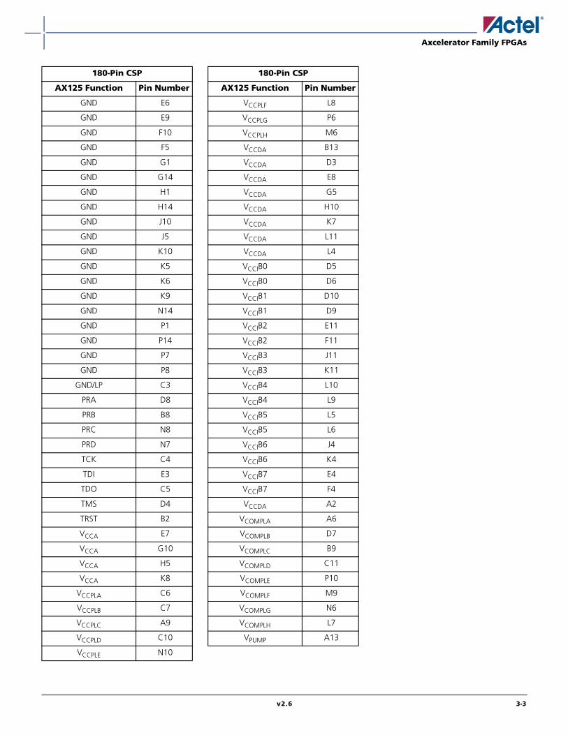
Axcelerator Family FPGAs
v2.6 3-3
GND E6
GND E9
GND F10
GND F5
GND G1
GND G14
GND H1
GND H14
GND J10
GND J5
GND K10
GND K5
GND K6
GND K9
GND N14
GND P1
GND P14
GND P7
GND P8
GND/LP C3
PRA D8
PRB B8
PRC N8
PRD N7
TCK C4
TDI E3
TDO C5
TMS D4
TRST B2
VCCA E7
VCCA G10
VCCA H5
VCCA K8
VCCPLA C6
VCCPLB C7
VCCPLC A9
VCCPLD C10
VCCPLE N10
180-Pin CSP
AX125 Function Pin Number
VCCPLF L8
VCCPLG P6
VCCPLH M6
VCCDA B13
VCCDA D3
VCCDA E8
VCCDA G5
VCCDA H10
VCCDA K7
VCCDA L11
VCCDA L4
VCCIB0 D5
VCCIB0 D6
VCCIB1 D10
VCCIB1 D9
VCCIB2 E11
VCCIB2 F11
VCCIB3 J11
VCCIB3 K11
VCCIB4 L10
VCCIB4 L9
VCCIB5 L5
VCCIB5 L6
VCCIB6 J4
VCCIB6 K4
VCCIB7 E4
VCCIB7 F4
VCCDA A2
VCOMPLA A6
VCOMPLB D7
VCOMPLC B9
VCOMPLD C11
VCOMPLE P10
VCOMPLF M9
VCOMPLG N6
VCOMPLH L7
VPUMP A13
180-Pin CSP
AX125 Function Pin Number

Axcelerator Family FPGAs
3-4 v2.6
729-Pin PBGA
NoteFor Package Manufacturing and Environmental information, visit Resource center athttp://www.actel.com/products/rescenter/package/index.html.
Figure 3-2 • 729-Pin PBGA (Bottom View)
A1 Ball Pad Corner
D
F
H
K
M
P
T
V
Y
AD
AFAG
E
G
J
L
N
R
U
W
AC
AE
BA
C
ABAA
13681012141620242627 18 2479111315192325 1722 21 5

Axcelerator Family FPGAs
v2.6 3-5
729-Pin PBGA
AX1000 Function Pin Number
Bank 0
IO00NB0F0 E6
IO00PB0F0 F6
IO01NB0F0 G8
IO01PB0F0 G7
IO02NB0F0 D7
IO02PB0F0 E7
IO03NB0F0 D5
IO03PB0F0 E5
IO04NB0F0 G9
IO04PB0F0 H9
IO05NB0F0 E8
IO05PB0F0 F8
IO06NB0F0 C6
IO06PB0F0 D6
IO07NB0F0 B5
IO07PB0F0 C5
IO08NB0F0 A6
IO08PB0F0 A5
IO09NB0F0 E9
IO09PB0F0 F9
IO10NB0F0 G10
IO10PB0F0 H10
IO11NB0F0 B7
IO11PB0F0 B6
IO12NB0F1 C8
IO12PB0F1 C7
IO13NB0F1 E10
IO13PB0F1 F10
IO14NB0F1 G11
IO14PB0F1 H11
IO15NB0F1 D9
IO15PB0F1 D8
IO16NB0F1 A8
IO16PB0F1 A7
IO17NB0F1 B9
IO17PB0F1 B8
IO18NB0F1 C10
IO18PB0F1 C9
IO19NB0F1 E11
IO19PB0F1 F11
IO20NB0F1 G12
IO20PB0F1 H12
IO21NB0F1 D11
IO21PB0F1 D10
IO22NB0F2 A10
IO22PB0F2 A9
IO23NB0F2 B11
IO23PB0F2 B10
IO24NB0F2 G13
IO24PB0F2 H13
IO25NB0F2 C12
IO25PB0F2 C11
IO26NB0F2 E12
IO26PB0F2 D12
IO27NB0F2 E13
IO27PB0F2 F13
IO28NB0F2 G14
IO28PB0F2 H14
IO29NB0F2 A12
IO29PB0F2 B12
IO30NB0F2/HCLKAN C13
IO30PB0F2/HCLKAP D13
IO31NB0F2/HCLKBN F14
IO31PB0F2/HCLKBP E14
Bank 1
IO32NB1F3/HCLKCN C14
IO32PB1F3/HCLKCP B14
IO33NB1F3/HCLKDN D16
IO33PB1F3/HCLKDP D15
IO34NB1F3 B16
IO34PB1F3 A16
IO35NB1F3 E15
IO35PB1F3 F15
IO36NB1F3 H15
IO36PB1F3 G15
729-Pin PBGA
AX1000 Function Pin Number
IO37NB1F3 C17
IO37PB1F3 C16
IO38NB1F3 B18
IO38PB1F3 B17
IO39NB1F3 A18
IO39PB1F3 A17
IO40NB1F3 H16
IO40PB1F3 G16
IO41NB1F4 B19
IO41PB1F4 A19
IO42NB1F4 C19
IO42PB1F4 C18
IO43NB1F4 D18
IO43PB1F4 D17
IO44NB1F4 H17
IO44PB1F4 G17
IO45NB1F4 F17
IO45PB1F4 E17
IO46NB1F4 B20
IO46PB1F4 A20
IO47NB1F4 C21
IO47PB1F4 C20
IO48NB1F4 H18
IO48PB1F4 G18
IO49NB1F4 F18
IO49PB1F4 E18
IO50NB1F4 D20
IO50PB1F4 D19
IO51NB1F4 A22
IO51PB1F4 A21
IO52NB1F4 B22
IO52PB1F4 B21
IO53NB1F4 F19
IO53PB1F4 E19
IO54NB1F5 F20
IO54PB1F5 E20
IO55NB1F5 E21
IO55PB1F5 D21
729-Pin PBGA
AX1000 Function Pin Number

Axcelerator Family FPGAs
3-6 v2.6
IO56NB1F5 H19
IO56PB1F5 G19
IO57NB1F5 D22
IO57PB1F5 C22
IO58NB1F5 B23
IO58PB1F5 A23
IO59NB1F5 D23
IO59PB1F5 C23
IO60NB1F5 G21
IO60PB1F5 G20
IO61NB1F5 E23
IO61PB1F5 E22
IO62NB1F5 F22
IO62PB1F5 F21
IO63NB1F5 H20
IO63PB1F5 J19
Bank 2
IO64NB2F6 J21
IO64PB2F6 H21
IO65NB2F6 F24
IO65PB2F6 F23
IO66NB2F6 F26
IO66PB2F6 F25
IO67NB2F6 E26
IO67PB2F6 E25
IO68NB2F6 J22
IO68PB2F6 H22
IO69NB2F6 G24
IO69PB2F6 G23
IO70NB2F6 K20
IO70PB2F6 J20
IO71NB2F6 G26
IO71PB2F6 G25
IO72NB2F6 J24
IO72PB2F6 J23
IO73NB2F6 H24
IO73PB2F6 H23
IO74NB2F7 L21
729-Pin PBGA
AX1000 Function Pin Number
IO74PB2F7 K21
IO75NB2F7 G27
IO75PB2F7 F27
IO76NB2F7 K23
IO76PB2F7 K22
IO77NB2F7 H26
IO77PB2F7 H25
IO78NB2F7 K25
IO78PB2F7 K24
IO79NB2F7 J26
IO79PB2F7 J25
IO80NB2F7 M20
IO80PB2F7 L20
IO81NB2F7 J27
IO81PB2F7 H27
IO82NB2F7 L23
IO82PB2F7 L22
IO83NB2F7 L25
IO83PB2F7 L24
IO84NB2F7 N21
IO84PB2F7 M21
IO85NB2F8 K27
IO85PB2F8 K26
IO86NB2F8 M23
IO86PB2F8 M22
IO87NB2F8 M25
IO87PB2F8 M24
IO88NB2F8 L27
IO88PB2F8 L26
IO89NB2F8 M27
IO89PB2F8 M26
IO90NB2F8 N23
IO90PB2F8 N22
IO91NB2F8 N25
IO91PB2F8 N24
IO92NB2F8 N27
IO92PB2F8 N26
IO93NB2F8 P26
729-Pin PBGA
AX1000 Function Pin Number
IO93PB2F8 P27
IO94NB2F8 N19
IO94PB2F8 N20
IO95NB2F8 P23
IO95PB2F8 P22
Bank 3
IO96NB3F9 P25
IO96PB3F9 P24
IO97NB3F9 R26
IO97PB3F9 R27
IO98NB3F9 P21
IO98PB3F9 P20
IO99NB3F9 R24
IO99PB3F9 R25
IO100NB3F9 T26
IO100PB3F9 T27
IO101NB3F9 T24
IO101PB3F9 T25
IO102NB3F9 R20
IO102PB3F9 R21
IO103NB3F9 R23
IO103PB3F9 R22
IO104NB3F9 U26
IO104PB3F9 U27
IO105NB3F9 U24
IO105PB3F9 U25
IO106NB3F9 R19
IO106PB3F9 P19
IO107NB3F10 V26
IO107PB3F10 V27
IO108NB3F10 T23
IO108PB3F10 T22
IO109NB3F10 V24
IO109PB3F10 V25
IO110NB3F10 T20
IO110PB3F10 T21
IO111NB3F10 W26
IO111PB3F10 W27
729-Pin PBGA
AX1000 Function Pin Number
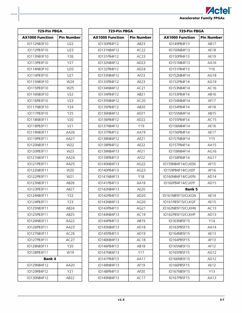
Axcelerator Family FPGAs
v2.6 3-7
IO112NB3F10 U22
IO112PB3F10 U23
IO113NB3F10 Y26
IO113PB3F10 Y27
IO114NB3F10 U20
IO114PB3F10 U21
IO115NB3F10 W24
IO115PB3F10 W25
IO116NB3F10 V22
IO116PB3F10 V23
IO117NB3F10 Y24
IO117PB3F10 Y25
IO118NB3F11 V20
IO118PB3F11 V21
IO119NB3F11 AA26
IO119PB3F11 AA27
IO120NB3F11 W22
IO120PB3F11 W23
IO121NB3F11 AA24
IO121PB3F11 AA25
IO122NB3F11 W20
IO122PB3F11 W21
IO123NB3F11 AB26
IO123PB3F11 AB27
IO124NB3F11 Y22
IO124PB3F11 Y23
IO125NB3F11 AB24
IO125PB3F11 AB25
IO126NB3F11 AA22
IO126PB3F11 AA23
IO127NB3F11 AC26
IO127PB3F11 AC27
IO128NB3F11 Y20
IO128PB3F11 W19
Bank 4
IO129NB4F12 AA20
IO129PB4F12 Y21
IO130NB4F12 AB22
729-Pin PBGA
AX1000 Function Pin Number
IO130PB4F12 AB23
IO131NB4F12 AC22
IO131PB4F12 AC23
IO132NB4F12 AD23
IO132PB4F12 AD24
IO133NB4F12 AF23
IO133PB4F12 AE23
IO134NB4F12 AC21
IO134PB4F12 AB21
IO135NB4F12 AC20
IO135PB4F12 AB20
IO136NB4F12 AD21
IO136PB4F12 AD22
IO137NB4F12 Y19
IO137PB4F12 AA19
IO138NB4F12 AE21
IO138PB4F12 AE22
IO139NB4F13 AF21
IO139PB4F13 AF22
IO140NB4F13 AG22
IO140PB4F13 AG23
IO141NB4F13 Y18
IO141PB4F13 AA18
IO142NB4F13 AE20
IO142PB4F13 AD20
IO143NB4F13 AG20
IO143PB4F13 AG21
IO144NB4F13 AC19
IO144PB4F13 AB19
IO145NB4F13 AD18
IO145PB4F13 AD19
IO146NB4F13 AC18
IO146PB4F13 AB18
IO147NB4F13 Y17
IO147PB4F13 AA17
IO148NB4F13 AF19
IO148PB4F13 AF20
IO149NB4F13 AC17
729-Pin PBGA
AX1000 Function Pin Number
IO149PB4F13 AB17
IO150NB4F13 AE18
IO150PB4F13 AE19
IO151NB4F13 AA16
IO151PB4F13 Y16
IO152NB4F14 AG18
IO152PB4F14 AG19
IO153NB4F14 AC16
IO153PB4F14 AB16
IO154NB4F14 AF17
IO154PB4F14 AF18
IO155NB4F14 AB15
IO155PB4F14 AC15
IO156NB4F14 AE16
IO156PB4F14 AE17
IO157NB4F14 Y15
IO157PB4F14 AA15
IO158NB4F14 AG16
IO158PB4F14 AG17
IO159NB4F14/CLKEN AF15
IO159PB4F14/CLKEP AF16
IO160NB4F14/CLKFN AD14
IO160PB4F14/CLKFP AD15
Bank 5
IO161NB5F15/CLKGN AE14
IO161PB5F15/CLKGP AE15
IO162NB5F15/CLKHN AC13
IO162PB5F15/CLKHP AD13
IO163NB5F15 Y14
IO163PB5F15 AA14
IO164NB5F15 AE13
IO164PB5F15 AF13
IO165NB5F15 AF12
IO165PB5F15 AG12
IO166NB5F15 AD12
IO166PB5F15 AE12
IO167NB5F15 Y13
IO167PB5F15 AA13
729-Pin PBGA
AX1000 Function Pin Number

Axcelerator Family FPGAs
3-8 v2.6
IO168NB5F15 AD11
IO168PB5F15 AE11
IO169NB5F15 AG11
IO169PB5F15 AF11
IO170NB5F15 AB11
IO170PB5F15 AC11
IO171NB5F16 AF10
IO171PB5F16 AG10
IO172NB5F16 AD10
IO172PB5F16 AE10
IO173NB5F16 Y12
IO173PB5F16 AA12
IO174NB5F16 AB10
IO174PB5F16 AC10
IO175NB5F16 AF9
IO175PB5F16 AG9
IO176NB5F16 AD9
IO176PB5F16 AE9
IO177NB5F16 Y11
IO177PB5F16 AA11
IO178NB5F16 AF8
IO178PB5F16 AG8
IO179NB5F16 AD8
IO179PB5F16 AE8
IO180NB5F16 AB9
IO180PB5F16 AC9
IO181NB5F17 Y10
IO181PB5F17 AA10
IO182NB5F17 AF7
IO182PB5F17 AG7
IO183NB5F17 AD7
IO183PB5F17 AE7
IO184NB5F17 AC7
IO184PB5F17 AC8
IO185NB5F17 AF6
IO185PB5F17 AG6
IO186NB5F17 AB7
IO186PB5F17 AB8
729-Pin PBGA
AX1000 Function Pin Number
IO187NB5F17 Y9
IO187PB5F17 AA9
IO188NB5F17 AD6
IO188PB5F17 AE6
IO189NB5F17 AB6
IO189PB5F17 AC6
IO190NB5F17 AF5
IO190PB5F17 AG5
IO191NB5F17 AA6
IO191PB5F17 AA7
IO192NB5F17 Y8
IO192PB5F17 AA8
Bank 6
IO193NB6F18 W8
IO193PB6F18 Y7
IO194NB6F18 AB5
IO194PB6F18 AC5
IO195NB6F18 AC2
IO195PB6F18 AC3
IO196NB6F18 AC4
IO196PB6F18 AD4
IO197NB6F18 Y5
IO197PB6F18 Y6
IO198NB6F18 AB3
IO198PB6F18 AB4
IO199NB6F18 V7
IO199PB6F18 W7
IO200NB6F18 AA4
IO200PB6F18 AA5
IO201NB6F18 W5
IO201PB6F18 W6
IO202NB6F18 AB1
IO202PB6F18 AC1
IO203NB6F19 Y3
IO203PB6F19 AA3
IO204NB6F19 AA2
IO204PB6F19 AB2
IO205NB6F19 U8
729-Pin PBGA
AX1000 Function Pin Number
IO205PB6F19 V8
IO206NB6F19 V5
IO206PB6F19 V6
IO207NB6F19 Y1
IO207PB6F19 AA1
IO208NB6F19 W4
IO208PB6F19 Y4
IO209NB6F19 T7
IO209PB6F19 U7
IO210NB6F19 W2
IO210PB6F19 Y2
IO211NB6F19 U5
IO211PB6F19 U6
IO212NB6F19 V3
IO212PB6F19 W3
IO213NB6F19 R9
IO213PB6F19 T8
IO214NB6F20 U4
IO214PB6F20 V4
IO215NB6F20 T5
IO215PB6F20 T6
IO216NB6F20 V1
IO216PB6F20 W1
IO217NB6F20 R7
IO217PB6F20 R8
IO218NB6F20 U2
IO218PB6F20 V2
IO219NB6F20 T1
IO219PB6F20 U1
IO220NB6F20 R5
IO220PB6F20 R6
IO221NB6F20 T3
IO221PB6F20 T4
IO222NB6F20 R2
IO222PB6F20 T2
IO223NB6F20 P8
IO223PB6F20 P9
IO224NB6F20 R3
729-Pin PBGA
AX1000 Function Pin Number

Axcelerator Family FPGAs
v2.6 3-9
IO224PB6F20 R4
Bank 7
IO225NB7F21 P1
IO225PB7F21 R1
IO226NB7F21 P3
IO226PB7F21 P2
IO227NB7F21 N7
IO227PB7F21 P7
IO228NB7F21 P5
IO228PB7F21 P4
IO229NB7F21 N2
IO229PB7F21 N1
IO230NB7F21 N6
IO230PB7F21 P6
IO231NB7F21 N9
IO231PB7F21 N8
IO232NB7F21 N4
IO232PB7F21 N3
IO233NB7F21 M2
IO233PB7F21 M1
IO234NB7F21 M4
IO234PB7F21 M3
IO235NB7F21 M5
IO235PB7F21 N5
IO236NB7F22 L2
IO236PB7F22 L1
IO237NB7F22 L4
IO237PB7F22 L3
IO238NB7F22 L6
IO238PB7F22 M6
IO239NB7F22 M8
IO239PB7F22 M7
IO240NB7F22 K2
IO240PB7F22 K1
IO241NB7F22 K4
IO241PB7F22 K3
IO242NB7F22 K5
IO242PB7F22 L5
729-Pin PBGA
AX1000 Function Pin Number
IO243NB7F22 J2
IO243PB7F22 J1
IO244NB7F22 J4
IO244PB7F22 J3
IO245NB7F22 H2
IO245PB7F22 H1
IO246NB7F22 H4
IO246PB7F22 H3
IO247NB7F23 L8
IO247PB7F23 L7
IO248NB7F23 J6
IO248PB7F23 K6
IO249NB7F23 H5
IO249PB7F23 J5
IO250NB7F23 G2
IO250PB7F23 G1
IO251NB7F23 K8
IO251PB7F23 K7
IO252NB7F23 G4
IO252PB7F23 G3
IO253NB7F23 F2
IO253PB7F23 F1
IO254NB7F23 G6
IO254PB7F23 H6
IO255NB7F23 F5
IO255PB7F23 G5
IO256NB7F23 F3
IO256PB7F23 F4
IO257NB7F23 H7
IO257PB7F23 J7
Dedicated I/O
GND A1
GND A2
GND A25
GND A26
GND A27
GND A3
GND AC24
729-Pin PBGA
AX1000 Function Pin Number
GND AE1
GND AE2
GND AE25
GND AE26
GND AE27
GND AE3
GND AE5
GND AF1
GND AF2
GND AF25
GND AF26
GND AF27
GND AF3
GND AG1
GND AG2
GND AG25
GND AG26
GND AG27
GND AG3
GND B1
GND B2
GND B25
GND B26
GND B27
GND B3
GND C1
GND C2
GND C25
GND C26
GND C27
GND C3
GND E27
GND L11
GND L12
GND L13
GND L14
GND L15
GND L16
729-Pin PBGA
AX1000 Function Pin Number
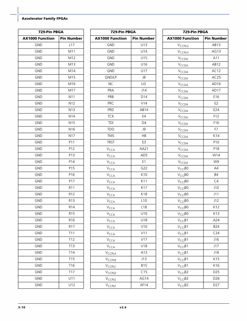
Axcelerator Family FPGAs
3-10 v2.6
GND L17
GND M11
GND M12
GND M13
GND M14
GND M15
GND M16
GND M17
GND N11
GND N12
GND N13
GND N14
GND N15
GND N16
GND N17
GND P11
GND P12
GND P13
GND P14
GND P15
GND P16
GND P17
GND R11
GND R12
GND R13
GND R14
GND R15
GND R16
GND R17
GND T11
GND T12
GND T13
GND T14
GND T15
GND T16
GND T17
GND U11
GND U12
729-Pin PBGA
AX1000 Function Pin Number
GND U13
GND U14
GND U15
GND U16
GND U17
GND/LP J8
NC U3
PRA J14
PRB D14
PRC V14
PRD AB14
TCK E4
TDI D4
TDO J9
TMS H8
TRST E3
VCCA AA21
VCCA AD5
VCCA E1
VCCA G22
VCCA K10
VCCA K11
VCCA K17
VCCA K18
VCCA L10
VCCA L18
VCCA U10
VCCA U18
VCCA V10
VCCA V11
VCCA V17
VCCA V18
VCCPLA A13
VCCPLB J13
VCCPLC B15
VCCPLD C15
VCCPLE AG14
VCCPLF AF14
729-Pin PBGA
AX1000 Function Pin Number
VCCPLG AB13
VCCPLH AG13
VCCDA A11
VCCDA AB12
VCCDA AC12
VCCDA AC25
VCCDA AD16
VCCDA AD17
VCCDA E16
VCCDA E2
VCCDA E24
VCCDA F12
VCCDA F16
VCCDA F7
VCCDA K14
VCCDA P10
VCCDA P18
VCCDA W14
VCCDA W9
VCCIB0 A4
VCCIB0 B4
VCCIB0 C4
VCCIB0 J10
VCCIB0 J11
VCCIB0 J12
VCCIB0 K12
VCCIB0 K13
VCCIB1 A24
VCCIB1 B24
VCCIB1 C24
VCCIB1 J16
VCCIB1 J17
VCCIB1 J18
VCCIB1 K15
VCCIB1 K16
VCCIB2 D25
VCCIB2 D26
VCCIB2 D27
729-Pin PBGA
AX1000 Function Pin Number

Axcelerator Family FPGAs
v2.6 3-11
VCCIB2 K19
VCCIB2 L19
VCCIB2 M18
VCCIB2 M19
VCCIB2 N18
VCCIB3 AD25
VCCIB3 AD26
VCCIB3 AD27
VCCIB3 R18
VCCIB3 T18
VCCIB3 T19
VCCIB3 U19
VCCIB3 V19
VCCIB4 AE24
VCCIB4 AF24
VCCIB4 AG24
VCCIB4 V15
VCCIB4 V16
VCCIB4 W16
VCCIB4 W17
VCCIB4 W18
VCCIB5 AE4
VCCIB5 AF4
VCCIB5 AG4
VCCIB5 V12
VCCIB5 V13
VCCIB5 W10
VCCIB5 W11
VCCIB5 W12
VCCIB6 AD1
VCCIB6 AD2
VCCIB6 AD3
VCCIB6 R10
VCCIB6 T10
VCCIB6 T9
VCCIB6 U9
VCCIB6 V9
VCCIB7 D1
729-Pin PBGA
AX1000 Function Pin Number
VCCIB7 D2
VCCIB7 D3
VCCIB7 K9
VCCIB7 L9
VCCIB7 M10
VCCIB7 M9
VCCIB7 N10
VCOMPLA B13
VCOMPLB A14
VCOMPLC A15
VCOMPLD J15
VCOMPLE AG15
VCOMPLF W15
VCOMPLG AC14
VCOMPLH W13
VPUMP D24
729-Pin PBGA
AX1000 Function Pin Number

Axcelerator Family FPGAs
3-12 v2.6
256-Pin FBGA
NoteFor Package Manufacturing and Environmental information, visit Resource center athttp://www.actel.com/products/rescenter/package/index.html.
Figure 3-3 • 256-Pin FBGA (Bottom View)
13579111315 246810121416
C
E
G
J
L
N
R
D
F
H
K
M
P
T
B
A
A1 Ball Pad Corner
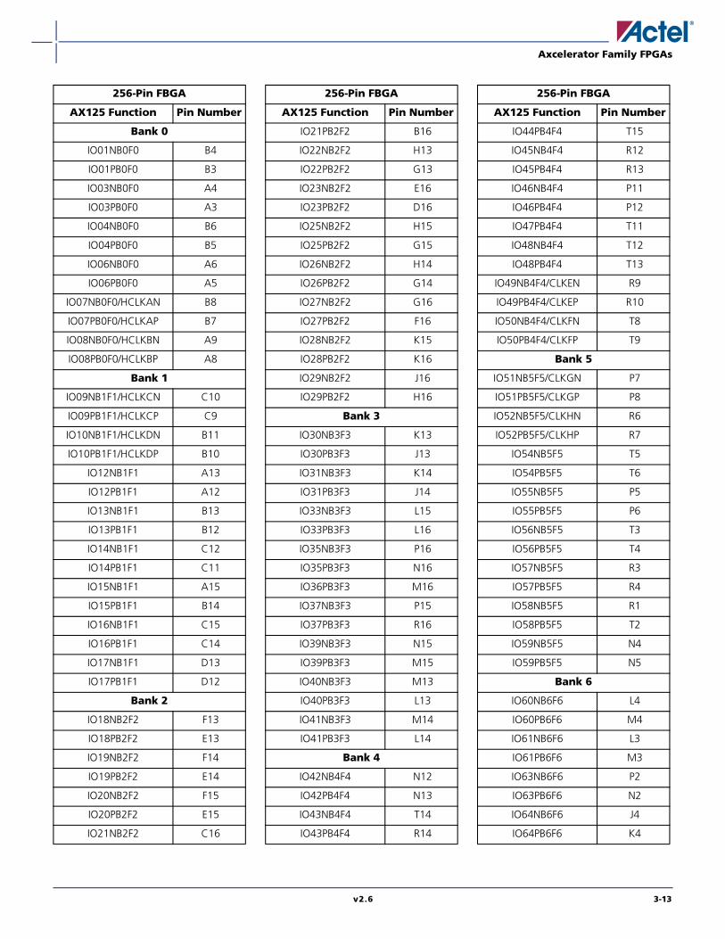
Axcelerator Family FPGAs
v2.6 3-13
256-Pin FBGA
AX125 Function Pin Number
Bank 0
IO01NB0F0 B4
IO01PB0F0 B3
IO03NB0F0 A4
IO03PB0F0 A3
IO04NB0F0 B6
IO04PB0F0 B5
IO06NB0F0 A6
IO06PB0F0 A5
IO07NB0F0/HCLKAN B8
IO07PB0F0/HCLKAP B7
IO08NB0F0/HCLKBN A9
IO08PB0F0/HCLKBP A8
Bank 1
IO09NB1F1/HCLKCN C10
IO09PB1F1/HCLKCP C9
IO10NB1F1/HCLKDN B11
IO10PB1F1/HCLKDP B10
IO12NB1F1 A13
IO12PB1F1 A12
IO13NB1F1 B13
IO13PB1F1 B12
IO14NB1F1 C12
IO14PB1F1 C11
IO15NB1F1 A15
IO15PB1F1 B14
IO16NB1F1 C15
IO16PB1F1 C14
IO17NB1F1 D13
IO17PB1F1 D12
Bank 2
IO18NB2F2 F13
IO18PB2F2 E13
IO19NB2F2 F14
IO19PB2F2 E14
IO20NB2F2 F15
IO20PB2F2 E15
IO21NB2F2 C16
IO21PB2F2 B16
IO22NB2F2 H13
IO22PB2F2 G13
IO23NB2F2 E16
IO23PB2F2 D16
IO25NB2F2 H15
IO25PB2F2 G15
IO26NB2F2 H14
IO26PB2F2 G14
IO27NB2F2 G16
IO27PB2F2 F16
IO28NB2F2 K15
IO28PB2F2 K16
IO29NB2F2 J16
IO29PB2F2 H16
Bank 3
IO30NB3F3 K13
IO30PB3F3 J13
IO31NB3F3 K14
IO31PB3F3 J14
IO33NB3F3 L15
IO33PB3F3 L16
IO35NB3F3 P16
IO35PB3F3 N16
IO36PB3F3 M16
IO37NB3F3 P15
IO37PB3F3 R16
IO39NB3F3 N15
IO39PB3F3 M15
IO40NB3F3 M13
IO40PB3F3 L13
IO41NB3F3 M14
IO41PB3F3 L14
Bank 4
IO42NB4F4 N12
IO42PB4F4 N13
IO43NB4F4 T14
IO43PB4F4 R14
256-Pin FBGA
AX125 Function Pin Number
IO44PB4F4 T15
IO45NB4F4 R12
IO45PB4F4 R13
IO46NB4F4 P11
IO46PB4F4 P12
IO47PB4F4 T11
IO48NB4F4 T12
IO48PB4F4 T13
IO49NB4F4/CLKEN R9
IO49PB4F4/CLKEP R10
IO50NB4F4/CLKFN T8
IO50PB4F4/CLKFP T9
Bank 5
IO51NB5F5/CLKGN P7
IO51PB5F5/CLKGP P8
IO52NB5F5/CLKHN R6
IO52PB5F5/CLKHP R7
IO54NB5F5 T5
IO54PB5F5 T6
IO55NB5F5 P5
IO55PB5F5 P6
IO56NB5F5 T3
IO56PB5F5 T4
IO57NB5F5 R3
IO57PB5F5 R4
IO58NB5F5 R1
IO58PB5F5 T2
IO59NB5F5 N4
IO59PB5F5 N5
Bank 6
IO60NB6F6 L4
IO60PB6F6 M4
IO61NB6F6 L3
IO61PB6F6 M3
IO63NB6F6 P2
IO63PB6F6 N2
IO64NB6F6 J4
IO64PB6F6 K4
256-Pin FBGA
AX125 Function Pin Number

Axcelerator Family FPGAs
3-14 v2.6
IO65NB6F6 N1
IO65PB6F6 P1
IO67NB6F6 L2
IO67PB6F6 M2
IO69NB6F6 L1
IO69PB6F6 M1
IO70NB6F6 J3
IO70PB6F6 K3
IO71NB6F6 J2
IO71PB6F6 K2
Bank 7
IO72NB7F7 J1
IO72PB7F7 K1
IO73NB7F7 G2
IO73PB7F7 H2
IO74NB7F7 G3
IO74PB7F7 H3
IO75NB7F7 E1
IO75PB7F7 F1
IO76NB7F7 G1
IO77NB7F7 E2
IO77PB7F7 F2
IO78NB7F7 G4
IO78PB7F7 H4
IO79NB7F7 C1
IO79PB7F7 D1
IO81NB7F7 C2
IO81PB7F7 B1
IO82NB7F7 D2
IO82PB7F7 D3
IO83NB7F7 E3
IO83PB7F7 F3
Dedicated I/O
VCCDA E4
GND A1
GND A16
GND B15
GND B2
256-Pin FBGA
AX125 Function Pin Number
GND D15
GND E12
GND E5
GND F11
GND F6
GND G10
GND G7
GND G8
GND G9
GND H10
GND H7
GND H8
GND H9
GND J10
GND J7
GND J8
GND J9
GND K10
GND K7
GND K8
GND K9
GND L11
GND L6
GND M12
GND M5
GND P13
GND P3
GND R15
GND R2
GND T1
GND T16
GND/LP D4
NC A11
NC R11
NC R5
PRA D8
PRB C8
PRC N9
256-Pin FBGA
AX125 Function Pin Number
PRD P9
TCK D5
TDI C6
TDO C4
TMS C3
TRST C5
VCCA D14
VCCA F10
VCCA F4
VCCA F7
VCCA F8
VCCA F9
VCCA G11
VCCA G6
VCCA H11
VCCA H6
VCCA J11
VCCA J6
VCCA K11
VCCA K6
VCCA L10
VCCA L7
VCCA L8
VCCA L9
VCCA N3
VCCA P14
VCCPLA C7
VCCPLB D6
VCCPLC A10
VCCPLD D10
VCCPLE P10
VCCPLF N11
VCCPLG T7
VCCPLH N7
VCCDA A2
VCCDA C13
VCCDA D9
VCCDA H1
256-Pin FBGA
AX125 Function Pin Number

Axcelerator Family FPGAs
v2.6 3-15
VCCDA J15
VCCDA N14
VCCDA N8
VCCDA P4
VCCIB0 E6
VCCIB0 E7
VCCIB0 E8
VCCIB1 E10
VCCIB1 E11
VCCIB1 E9
VCCIB2 F12
VCCIB2 G12
VCCIB2 H12
VCCIB3 J12
VCCIB3 K12
VCCIB3 L12
VCCIB4 M10
VCCIB4 M11
VCCIB4 M9
VCCIB5 M6
VCCIB5 M7
VCCIB5 M8
VCCIB6 J5
VCCIB6 K5
VCCIB6 L5
VCCIB7 F5
VCCIB7 G5
VCCIB7 H5
VCOMPLA A7
VCOMPLB D7
VCOMPLC B9
VCOMPLD D11
VCOMPLE T10
VCOMPLF N10
VCOMPLG R8
VCOMPLH N6
VPUMP A14
256-Pin FBGA
AX125 Function Pin Number
256-Pin FBGA
AX250 Function Pin Number
Bank 0
IO01NB0F0 B4
IO01PB0F0 B3
IO03NB0F0 A4
IO03PB0F0 A3
IO05NB0F0 B6
IO05PB0F0 B5
IO07NB0F0 A6
IO07PB0F0 A5
IO12NB0F0/HCLKAN B8
IO12PB0F0/HCLKAP B7
IO13NB0F0/HCLKBN A9
IO13PB0F0/HCLKBP A8
Bank 1
IO14NB1F1/HCLKCN C10
IO14PB1F1/HCLKCP C9
IO15NB1F1/HCLKDN B11
IO15PB1F1/HCLKDP B10
IO17NB1F1 A13
IO17PB1F1 A12
IO19NB1F1 B13
IO19PB1F1 B12
IO21NB1F1 C12
IO21PB1F1 C11
IO23NB1F1 A15
IO23PB1F1 B14
IO26NB1F1 C15
IO26PB1F1 C14
IO27NB1F1 D13
IO27PB1F1 D12
Bank 2
IO29NB2F2 F13
IO29PB2F2 E13
IO30NB2F2 F14
IO30PB2F2 E14
IO32NB2F2 C16
IO32PB2F2 B16
IO33NB2F2 F15
IO33PB2F2 E15
IO35NB2F2 H13
IO35PB2F2 G13
IO36NB2F2 E16
IO36PB2F2 D16
IO38NB2F2 H15
IO38PB2F2 G15
IO39NB2F2 H14
IO39PB2F2 G14
IO40NB2F2 G16
IO40PB2F2 F16
IO43NB2F2 K15
IO43PB2F2 K16
IO44NB2F2 J16
IO44PB2F2 H16
Bank 3
IO45NB3F3 K13
IO45PB3F3 J13
IO46NB3F3 K14
IO46PB3F3 J14
IO52NB3F3 L15
IO52PB3F3 L16
IO54NB3F3 P16
IO54PB3F3 N16
IO55PB3F3 M16
IO56NB3F3 P15
IO56PB3F3 R16
IO58NB3F3 N15
IO58PB3F3 M15
IO59NB3F3 M13
IO59PB3F3 L13
IO61NB3F3 M14
IO61PB3F3 L14
Bank 4
IO62NB4F4 N12
IO62PB4F4 N13
IO63NB4F4 T14
IO63PB4F4 R14
256-Pin FBGA
AX250 Function Pin Number
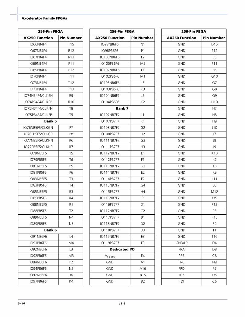
Axcelerator Family FPGAs
3-16 v2.6
IO66PB4F4 T15
IO67NB4F4 R12
IO67PB4F4 R13
IO69NB4F4 P11
IO69PB4F4 P12
IO70PB4F4 T11
IO73NB4F4 T12
IO73PB4F4 T13
IO74NB4F4/CLKEN R9
IO74PB4F4/CLKEP R10
IO75NB4F4/CLKFN T8
IO75PB4F4/CLKFP T9
Bank 5
IO76NB5F5/CLKGN P7
IO76PB5F5/CLKGP P8
IO77NB5F5/CLKHN R6
IO77PB5F5/CLKHP R7
IO79NB5F5 T5
IO79PB5F5 T6
IO81NB5F5 P5
IO81PB5F5 P6
IO83NB5F5 T3
IO83PB5F5 T4
IO85NB5F5 R3
IO85PB5F5 R4
IO88NB5F5 R1
IO88PB5F5 T2
IO89NB5F5 N4
IO89PB5F5 N5
Bank 6
IO91NB6F6 L4
IO91PB6F6 M4
IO92NB6F6 L3
IO92PB6F6 M3
IO94NB6F6 P2
IO94PB6F6 N2
IO97NB6F6 J4
IO97PB6F6 K4
256-Pin FBGA
AX250 Function Pin Number
IO98NB6F6 N1
IO98PB6F6 P1
IO100NB6F6 L2
IO100PB6F6 M2
IO102NB6F6 L1
IO102PB6F6 M1
IO103NB6F6 J3
IO103PB6F6 K3
IO104NB6F6 J2
IO104PB6F6 K2
Bank 7
IO107NB7F7 J1
IO107PB7F7 K1
IO108NB7F7 G2
IO108PB7F7 H2
IO111NB7F7 G3
IO111PB7F7 H3
IO112NB7F7 E1
IO112PB7F7 F1
IO113NB7F7 G1
IO114NB7F7 E2
IO114PB7F7 F2
IO115NB7F7 G4
IO115PB7F7 H4
IO116NB7F7 C1
IO116PB7F7 D1
IO117NB7F7 C2
IO117PB7F7 B1
IO118NB7F7 D2
IO118PB7F7 D3
IO119NB7F7 E3
IO119PB7F7 F3
Dedicated I/O
VCCDA E4
GND A1
GND A16
GND B15
GND B2
256-Pin FBGA
AX250 Function Pin Number
GND D15
GND E12
GND E5
GND F11
GND F6
GND G10
GND G7
GND G8
GND G9
GND H10
GND H7
GND H8
GND H9
GND J10
GND J7
GND J8
GND J9
GND K10
GND K7
GND K8
GND K9
GND L11
GND L6
GND M12
GND M5
GND P13
GND P3
GND R15
GND R2
GND T1
GND T16
GND/LP D4
PRA D8
PRB C8
PRC N9
PRD P9
TCK D5
TDI C6
256-Pin FBGA
AX250 Function Pin Number

Axcelerator Family FPGAs
v2.6 3-17
TDO C4
TMS C3
TRST C5
VCCA D14
VCCA F10
VCCA F4
VCCA F7
VCCA F8
VCCA F9
VCCA G11
VCCA G6
VCCA H11
VCCA H6
VCCA J11
VCCA J6
VCCA K11
VCCA K6
VCCA L10
VCCA L7
VCCA L8
VCCA L9
VCCA N3
VCCA P14
VCCPLA C7
VCCPLB D6
VCCPLC A10
VCCPLD D10
VCCPLE P10
VCCPLF N11
VCCPLG T7
VCCPLH N7
VCCDA A11
VCCDA A2
VCCDA C13
VCCDA D9
VCCDA H1
VCCDA J15
VCCDA N14
256-Pin FBGA
AX250 Function Pin Number
VCCDA N8
VCCDA P4
VCCDA R11
VCCDA R5
VCCIB0 E6
VCCIB0 E7
VCCIB0 E8
VCCIB1 E10
VCCIB1 E11
VCCIB1 E9
VCCIB2 F12
VCCIB2 G12
VCCIB2 H12
VCCIB3 J12
VCCIB3 K12
VCCIB3 L12
VCCIB4 M10
VCCIB4 M11
VCCIB4 M9
VCCIB5 M6
VCCIB5 M7
VCCIB5 M8
VCCIB6 J5
VCCIB6 K5
VCCIB6 L5
VCCIB7 F5
VCCIB7 G5
VCCIB7 H5
VCOMPLA A7
VCOMPLB D7
VCOMPLC B9
VCOMPLD D11
VCOMPLE T10
VCOMPLF N10
VCOMPLG R8
VCOMPLH N6
VPUMP A14
256-Pin FBGA
AX250 Function Pin Number

Axcelerator Family FPGAs
3-18 v2.6
324-Pin FBGA
NoteFor Package Manufacturing and Environmental information, visit Resource center athttp://www.actel.com/products/rescenter/package/index.html.
Figure 3-4 • 324-Pin FBGA (Bottom View)
13579111315 246810121416
C
E
G
J
L
N
R
D
F
H
K
M
P
T
B
A
1718
UV
A1 Ball Pad Corner

Axcelerator Family FPGAs
v2.6 3-19
324-Pin FBGA
AX125 Function Pin Number
Bank 0
IO00NB0F0 C5
IO00PB0F0 C4
IO01NB0F0 A3
IO01PB0F0 A2
IO02NB0F0 C7
IO02PB0F0 C6
IO03NB0F0 B5
IO03PB0F0 B4
IO04NB0F0 A5
IO04PB0F0 A4
IO05NB0F0 A7
IO05PB0F0 A6
IO06NB0F0 B7
IO06PB0F0 B6
IO07NB0F0/HCLKAN C9
IO07PB0F0/HCLKAP C8
IO08NB0F0/HCLKBN B10
IO08PB0F0/HCLKBP B9
Bank 1
IO09NB1F1/HCLKCN D11
IO09PB1F1/HCLKCP D10
IO10NB1F1/HCLKDN C12
IO10PB1F1/HCLKDP C11
IO11NB1F1 A15
IO11PB1F1 A14
IO12NB1F1 B14
IO12PB1F1 B13
IO13NB1F1 A17
IO13PB1F1 A16
IO14NB1F1 D13
IO14PB1F1 D12
IO15NB1F1 C14
IO15PB1F1 C13
IO16NB1F1 B16
IO16PB1F1 C15
IO17NB1F1 E14
IO17PB1F1 E13
Bank 2
IO18NB2F2 G14
IO18PB2F2 F14
IO19NB2F2 D16
IO19PB2F2 D15
IO20NB2F2 C18
IO20PB2F2 B18
IO21NB2F2 D17
IO21PB2F2 C17
IO22NB2F2 F17
IO22PB2F2 E17
IO23NB2F2 G16
IO23PB2F2 F16
IO24NB2F2 E18
IO24PB2F2 D18
IO25NB2F2 G18
IO25PB2F2 F18
IO26NB2F2 H17
IO26PB2F2 G17
IO27NB2F2 J16
IO27PB2F2 H16
IO28NB2F2 J18
IO28PB2F2 H18
IO29NB2F2 K17
IO29PB2F2 J17
Bank 3
IO30NB3F3 N18
IO30PB3F3 M18
IO31NB3F3 L18
IO31PB3F3 K18
IO32NB3F3 L16
IO32PB3F3 L17
IO33NB3F3 R18
IO33PB3F3 P18
IO34NB3F3 N15
IO34PB3F3 M15
IO35NB3F3 M16
IO35PB3F3 M17
324-Pin FBGA
AX125 Function Pin Number
IO36NB3F3 P16
IO36PB3F3 N16
IO37NB3F3 R17
IO37PB3F3 P17
IO38NB3F3 N14
IO38PB3F3 M14
IO39NB3F3 U18
IO39PB3F3 T18
IO40NB3F3 R16
IO40PB3F3 T17
IO41NB3F3 P13
IO41PB3F3 P14
Bank 4
IO42NB4F4 T13
IO42PB4F4 T14
IO43NB4F4 U15
IO43PB4F4 T15
IO44NB4F4 U13
IO44PB4F4 U14
IO45NB4F4 V15
IO45PB4F4 V16
IO46NB4F4 V13
IO46PB4F4 V14
IO47NB4F4 V12
IO47PB4F4 U12
IO48NB4F4 V10
IO48PB4F4 V11
IO49NB4F4/CLKEN T10
IO49PB4F4/CLKEP T11
IO50NB4F4/CLKFN U9
IO50PB4F4/CLKFP U10
Bank 5
IO51NB5F5/CLKGN R8
IO51PB5F5/CLKGP R9
IO52NB5F5/CLKHN T7
IO52PB5F5/CLKHP T8
IO53NB5F5 U6
IO53PB5F5 U7
324-Pin FBGA
AX125 Function Pin Number
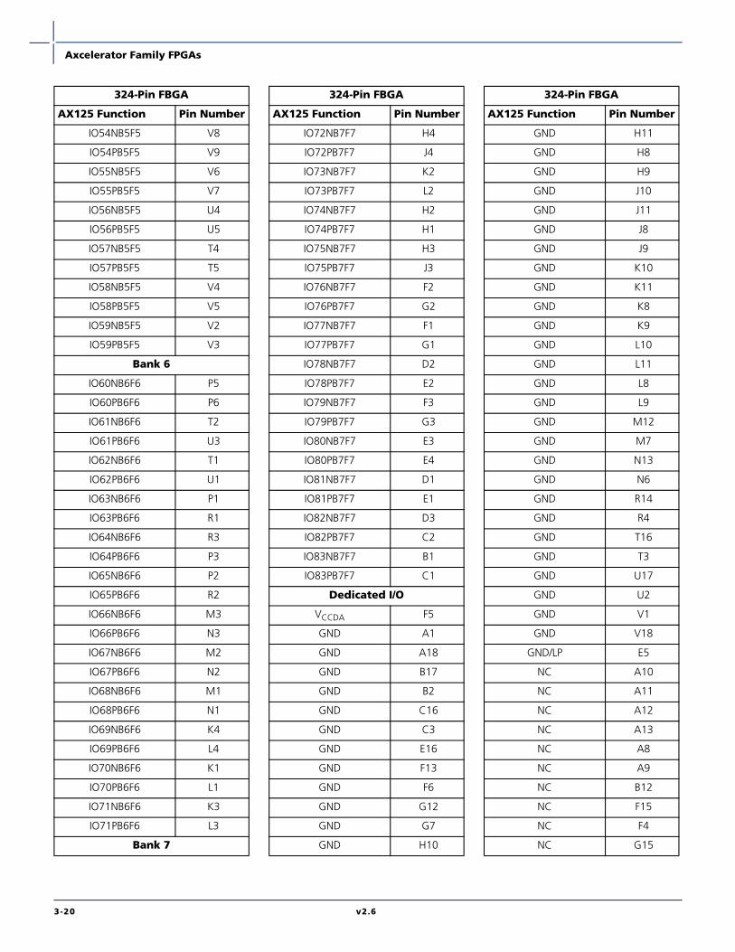
Axcelerator Family FPGAs
3-20 v2.6
IO54NB5F5 V8
IO54PB5F5 V9
IO55NB5F5 V6
IO55PB5F5 V7
IO56NB5F5 U4
IO56PB5F5 U5
IO57NB5F5 T4
IO57PB5F5 T5
IO58NB5F5 V4
IO58PB5F5 V5
IO59NB5F5 V2
IO59PB5F5 V3
Bank 6
IO60NB6F6 P5
IO60PB6F6 P6
IO61NB6F6 T2
IO61PB6F6 U3
IO62NB6F6 T1
IO62PB6F6 U1
IO63NB6F6 P1
IO63PB6F6 R1
IO64NB6F6 R3
IO64PB6F6 P3
IO65NB6F6 P2
IO65PB6F6 R2
IO66NB6F6 M3
IO66PB6F6 N3
IO67NB6F6 M2
IO67PB6F6 N2
IO68NB6F6 M1
IO68PB6F6 N1
IO69NB6F6 K4
IO69PB6F6 L4
IO70NB6F6 K1
IO70PB6F6 L1
IO71NB6F6 K3
IO71PB6F6 L3
Bank 7
324-Pin FBGA
AX125 Function Pin Number
IO72NB7F7 H4
IO72PB7F7 J4
IO73NB7F7 K2
IO73PB7F7 L2
IO74NB7F7 H2
IO74PB7F7 H1
IO75NB7F7 H3
IO75PB7F7 J3
IO76NB7F7 F2
IO76PB7F7 G2
IO77NB7F7 F1
IO77PB7F7 G1
IO78NB7F7 D2
IO78PB7F7 E2
IO79NB7F7 F3
IO79PB7F7 G3
IO80NB7F7 E3
IO80PB7F7 E4
IO81NB7F7 D1
IO81PB7F7 E1
IO82NB7F7 D3
IO82PB7F7 C2
IO83NB7F7 B1
IO83PB7F7 C1
Dedicated I/O
VCCDA F5
GND A1
GND A18
GND B17
GND B2
GND C16
GND C3
GND E16
GND F13
GND F6
GND G12
GND G7
GND H10
324-Pin FBGA
AX125 Function Pin Number
GND H11
GND H8
GND H9
GND J10
GND J11
GND J8
GND J9
GND K10
GND K11
GND K8
GND K9
GND L10
GND L11
GND L8
GND L9
GND M12
GND M7
GND N13
GND N6
GND R14
GND R4
GND T16
GND T3
GND U17
GND U2
GND V1
GND V18
GND/LP E5
NC A10
NC A11
NC A12
NC A13
NC A8
NC A9
NC B12
NC F15
NC F4
NC G15
324-Pin FBGA
AX125 Function Pin Number

Axcelerator Family FPGAs
v2.6 3-21
NC G4
NC H14
NC H15
NC H5
NC J1
NC J14
NC J15
NC J5
NC K14
NC K15
NC K5
NC L14
NC L15
NC L5
NC M4
NC M5
NC N17
NC N4
NC N5
NC R12
NC R13
NC R6
NC R7
NC T12
NC T6
NC U16
NC V17
PRA E9
PRB D9
PRC P10
PRD R10
TCK E6
TDI D7
TDO D5
TMS D4
TRST D6
VCCA E15
VCCA G10
324-Pin FBGA
AX125 Function Pin Number
VCCA G11
VCCA G5
VCCA G8
VCCA G9
VCCA H12
VCCA H7
VCCA J12
VCCA J7
VCCA K12
VCCA K7
VCCA L12
VCCA L7
VCCA M10
VCCA M11
VCCA M8
VCCA M9
VCCA P4
VCCA R15
VCCPLA D8
VCCPLB E7
VCCPLC B11
VCCPLD E11
VCCPLE R11
VCCPLF P12
VCCPLG U8
VCCPLH P8
VCCDA B3
VCCDA D14
VCCDA E10
VCCDA J2
VCCDA K16
VCCDA P15
VCCDA P9
VCCDA R5
VCCIB0 F7
VCCIB0 F8
VCCIB0 F9
VCCIB1 F10
324-Pin FBGA
AX125 Function Pin Number
VCCIB1 F11
VCCIB1 F12
VCCIB2 G13
VCCIB2 H13
VCCIB2 J13
VCCIB3 K13
VCCIB3 L13
VCCIB3 M13
VCCIB4 N10
VCCIB4 N11
VCCIB4 N12
VCCIB5 N7
VCCIB5 N8
VCCIB5 N9
VCCIB6 K6
VCCIB6 L6
VCCIB6 M6
VCCIB7 G6
VCCIB7 H6
VCCIB7 J6
VCOMPLA B8
VCOMPLB E8
VCOMPLC C10
VCOMPLD E12
VCOMPLE U11
VCOMPLF P11
VCOMPLG T9
VCOMPLH P7
VPUMP B15
324-Pin FBGA
AX125 Function Pin Number
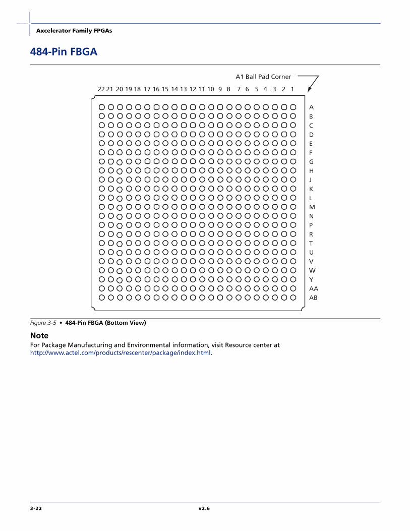
Axcelerator Family FPGAs
3-22 v2.6
484-Pin FBGA
NoteFor Package Manufacturing and Environmental information, visit Resource center athttp://www.actel.com/products/rescenter/package/index.html.
Figure 3-5 • 484-Pin FBGA (Bottom View)
A
BCDEFGHJKLMNPRTUVWYAAAB
12345678910111213141516171819202122
A1 Ball Pad Corner

Axcelerator Family FPGAs
v2.6 3-23
484-Pin FBGA
AX250 Function Pin Number
Bank 0
IO00NB0F0 D7
IO00PB0F0 D6
IO01NB0F0 E7
IO01PB0F0 E6
IO02NB0F0 C5
IO02PB0F0 C4
IO03NB0F0 C7
IO03PB0F0 C6
IO04NB0F0 E9
IO04PB0F0 E8
IO05NB0F0 D9
IO05PB0F0 D8
IO06NB0F0 B7
IO06PB0F0 B6
IO07NB0F0 C9
IO07PB0F0 C8
IO08NB0F0 A7
IO08PB0F0 A6
IO09NB0F0 B9
IO09PB0F0 B8
IO10NB0F0 A9
IO10PB0F0 A8
IO11NB0F0 B10
IO11PB0F0 A10
IO12NB0F0/HCLKAN E11
IO12PB0F0/HCLKAP E10
IO13NB0F0/HCLKBN D12
IO13PB0F0/HCLKBP D11
Bank 1
IO14NB1F1/HCLKCN F13
IO14PB1F1/HCLKCP F12
IO15NB1F1/HCLKDN E14
IO15PB1F1/HCLKDP E13
IO16NB1F1 C13
IO16PB1F1 C12
IO17NB1F1 B14
IO17PB1F1 B13
IO18NB1F1 A14
IO18PB1F1 A13
IO19NB1F1 A16
IO19PB1F1 A15
IO20NB1F1 B16
IO20PB1F1 B15
IO21NB1F1 C17
IO21PB1F1 C16
IO22NB1F1 F15
IO22PB1F1 F14
IO23NB1F1 D16
IO23PB1F1 D15
IO24NB1F1 E16
IO24PB1F1 E15
IO25NB1F1 F18
IO25PB1F1 F17
IO26NB1F1 D18
IO26PB1F1 E17
IO27NB1F1 G16
IO27PB1F1 G15
Bank 2
IO28NB2F2 F19
IO28PB2F2 E19
IO29NB2F2 J16
IO29PB2F2 H16
IO30NB2F2 E20
IO30PB2F2 D20
IO31NB2F2 J17
IO31PB2F2 H17
IO32NB2F2 G20
IO32PB2F2 F20
IO33NB2F2 H19
IO33PB2F2 G19
IO34NB2F2 E22
IO34PB2F2 D22
IO35NB2F2 J18
IO35PB2F2 H18
IO36NB2F2 G21
484-Pin FBGA
AX250 Function Pin Number
IO36PB2F2 F21
IO37NB2F2 K19
IO37PB2F2 J19
IO38NB2F2 J20
IO38PB2F2 H20
IO39NB2F2 L16
IO39PB2F2 K16
IO40NB2F2 J21
IO40PB2F2 H21
IO41NB2F2 L17
IO41PB2F2 K17
IO42NB2F2 J22
IO42PB2F2 H22
IO43NB2F2 L18
IO43PB2F2 K18
IO44NB2F2 L20
IO44PB2F2 K20
Bank 3
IO45NB3F3 M19
IO45PB3F3 L19
IO46NB3F3 M21
IO46PB3F3 L21
IO47NB3F3 N17
IO47PB3F3 M17
IO48NB3F3 N18
IO48PB3F3 N19
IO49NB3F3 N16
IO49PB3F3 M16
IO50NB3F3 N20
IO50PB3F3 M20
IO51NB3F3 P21
IO51PB3F3 N21
IO52NB3F3 P18
IO52PB3F3 P19
IO53NB3F3 R20
IO53PB3F3 P20
IO54NB3F3 T21
IO54PB3F3 R21
484-Pin FBGA
AX250 Function Pin Number
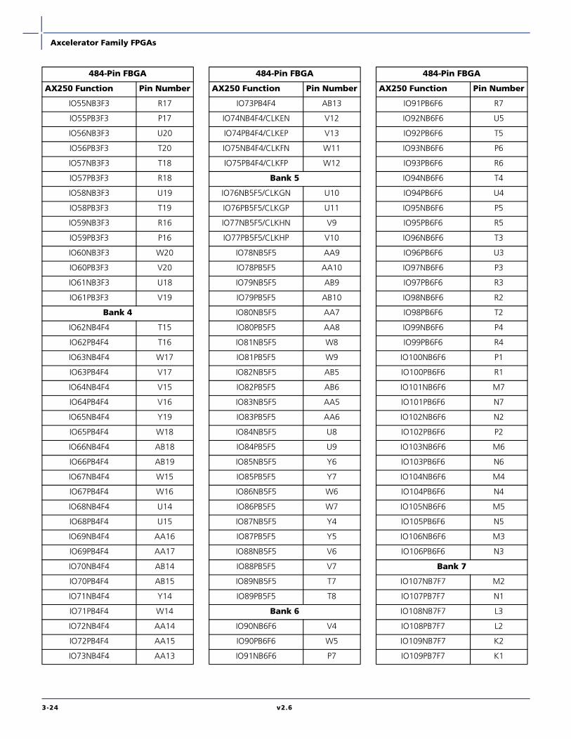
Axcelerator Family FPGAs
3-24 v2.6
IO55NB3F3 R17
IO55PB3F3 P17
IO56NB3F3 U20
IO56PB3F3 T20
IO57NB3F3 T18
IO57PB3F3 R18
IO58NB3F3 U19
IO58PB3F3 T19
IO59NB3F3 R16
IO59PB3F3 P16
IO60NB3F3 W20
IO60PB3F3 V20
IO61NB3F3 U18
IO61PB3F3 V19
Bank 4
IO62NB4F4 T15
IO62PB4F4 T16
IO63NB4F4 W17
IO63PB4F4 V17
IO64NB4F4 V15
IO64PB4F4 V16
IO65NB4F4 Y19
IO65PB4F4 W18
IO66NB4F4 AB18
IO66PB4F4 AB19
IO67NB4F4 W15
IO67PB4F4 W16
IO68NB4F4 U14
IO68PB4F4 U15
IO69NB4F4 AA16
IO69PB4F4 AA17
IO70NB4F4 AB14
IO70PB4F4 AB15
IO71NB4F4 Y14
IO71PB4F4 W14
IO72NB4F4 AA14
IO72PB4F4 AA15
IO73NB4F4 AA13
484-Pin FBGA
AX250 Function Pin Number
IO73PB4F4 AB13
IO74NB4F4/CLKEN V12
IO74PB4F4/CLKEP V13
IO75NB4F4/CLKFN W11
IO75PB4F4/CLKFP W12
Bank 5
IO76NB5F5/CLKGN U10
IO76PB5F5/CLKGP U11
IO77NB5F5/CLKHN V9
IO77PB5F5/CLKHP V10
IO78NB5F5 AA9
IO78PB5F5 AA10
IO79NB5F5 AB9
IO79PB5F5 AB10
IO80NB5F5 AA7
IO80PB5F5 AA8
IO81NB5F5 W8
IO81PB5F5 W9
IO82NB5F5 AB5
IO82PB5F5 AB6
IO83NB5F5 AA5
IO83PB5F5 AA6
IO84NB5F5 U8
IO84PB5F5 U9
IO85NB5F5 Y6
IO85PB5F5 Y7
IO86NB5F5 W6
IO86PB5F5 W7
IO87NB5F5 Y4
IO87PB5F5 Y5
IO88NB5F5 V6
IO88PB5F5 V7
IO89NB5F5 T7
IO89PB5F5 T8
Bank 6
IO90NB6F6 V4
IO90PB6F6 W5
IO91NB6F6 P7
484-Pin FBGA
AX250 Function Pin Number
IO91PB6F6 R7
IO92NB6F6 U5
IO92PB6F6 T5
IO93NB6F6 P6
IO93PB6F6 R6
IO94NB6F6 T4
IO94PB6F6 U4
IO95NB6F6 P5
IO95PB6F6 R5
IO96NB6F6 T3
IO96PB6F6 U3
IO97NB6F6 P3
IO97PB6F6 R3
IO98NB6F6 R2
IO98PB6F6 T2
IO99NB6F6 P4
IO99PB6F6 R4
IO100NB6F6 P1
IO100PB6F6 R1
IO101NB6F6 M7
IO101PB6F6 N7
IO102NB6F6 N2
IO102PB6F6 P2
IO103NB6F6 M6
IO103PB6F6 N6
IO104NB6F6 M4
IO104PB6F6 N4
IO105NB6F6 M5
IO105PB6F6 N5
IO106NB6F6 M3
IO106PB6F6 N3
Bank 7
IO107NB7F7 M2
IO107PB7F7 N1
IO108NB7F7 L3
IO108PB7F7 L2
IO109NB7F7 K2
IO109PB7F7 K1
484-Pin FBGA
AX250 Function Pin Number

Axcelerator Family FPGAs
v2.6 3-25
IO110NB7F7 K5
IO110PB7F7 L5
IO111NB7F7 K6
IO111PB7F7 L6
IO112NB7F7 K4
IO112PB7F7 K3
IO113NB7F7 K7
IO113PB7F7 L7
IO114NB7F7 H1
IO114PB7F7 J1
IO115NB7F7 H2
IO115PB7F7 J2
IO116NB7F7 H4
IO116PB7F7 J4
IO117NB7F7 H5
IO117PB7F7 J5
IO118NB7F7 F2
IO118PB7F7 G2
IO119NB7F7 H6
IO119PB7F7 J6
IO120NB7F7 F1
IO120PB7F7 G1
IO121NB7F7 F4
IO121PB7F7 G4
IO122NB7F7 G5
IO122PB7F7 G6
IO123NB7F7 F5
IO123PB7F7 E4
Dedicated I/O
VCCDA H7
GND A1
GND A11
GND A12
GND A2
GND A21
GND A22
GND AA1
GND AA2
484-Pin FBGA
AX250 Function Pin Number
GND AA21
GND AA22
GND AB1
GND AB11
GND AB12
GND AB2
GND AB21
GND AB22
GND B1
GND B2
GND B21
GND B22
GND C20
GND C3
GND D19
GND D4
GND E18
GND E5
GND G18
GND H15
GND H8
GND J14
GND J9
GND K10
GND K11
GND K12
GND K13
GND L1
GND L10
GND L11
GND L12
GND L13
GND L22
GND M1
GND M10
GND M11
GND M12
GND M13
484-Pin FBGA
AX250 Function Pin Number
GND M22
GND N10
GND N11
GND N12
GND N13
GND P14
GND P9
GND R15
GND R8
GND U16
GND U6
GND V18
GND V5
GND W19
GND W4
GND Y20
GND Y3
GND/LP G7
NC A17
NC A18
NC A19
NC A4
NC A5
NC AA11
NC AA12
NC AA18
NC AA19
NC AA4
NC AB16
NC AB17
NC AB4
NC AB7
NC AB8
NC B11
NC B12
NC B17
NC B18
NC B19
484-Pin FBGA
AX250 Function Pin Number
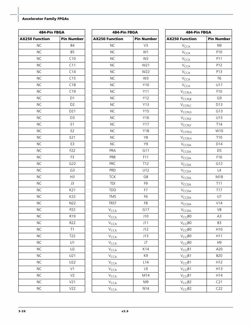
Axcelerator Family FPGAs
3-26 v2.6
NC B4
NC B5
NC C10
NC C11
NC C14
NC C15
NC C18
NC C19
NC D1
NC D2
NC D21
NC D3
NC E1
NC E2
NC E21
NC E3
NC F22
NC F3
NC G22
NC G3
NC H3
NC J3
NC K21
NC K22
NC N22
NC P22
NC R19
NC R22
NC T1
NC T22
NC U1
NC U2
NC U21
NC U22
NC V1
NC V2
NC V21
NC V22
484-Pin FBGA
AX250 Function Pin Number
NC V3
NC W1
NC W2
NC W21
NC W22
NC W3
NC Y10
NC Y11
NC Y12
NC Y13
NC Y15
NC Y16
NC Y17
NC Y18
NC Y8
NC Y9
PRA G11
PRB F11
PRC T12
PRD U12
TCK G8
TDI F9
TDO F7
TMS F6
TRST F8
VCCA G17
VCCA J10
VCCA J11
VCCA J12
VCCA J13
VCCA J7
VCCA K14
VCCA K9
VCCA L14
VCCA L9
VCCA M14
VCCA M9
VCCA N14
484-Pin FBGA
AX250 Function Pin Number
VCCA N9
VCCA P10
VCCA P11
VCCA P12
VCCA P13
VCCA T6
VCCA U17
VCCPLA F10
VCCPLB G9
VCCPLC D13
VCCPLD G13
VCCPLE U13
VCCPLF T14
VCCPLG W10
VCCPLH T10
VCCDA D14
VCCDA D5
VCCDA F16
VCCDA G12
VCCDA L4
VCCDA M18
VCCDA T11
VCCDA T17
VCCDA U7
VCCDA V14
VCCDA V8
VCCIB0 A3
VCCIB0 B3
VCCIB0 H10
VCCIB0 H11
VCCIB0 H9
VCCIB1 A20
VCCIB1 B20
VCCIB1 H12
VCCIB1 H13
VCCIB1 H14
VCCIB2 C21
VCCIB2 C22
484-Pin FBGA
AX250 Function Pin Number

Axcelerator Family FPGAs
v2.6 3-27
VCCIB2 J15
VCCIB2 K15
VCCIB2 L15
VCCIB3 M15
VCCIB3 N15
VCCIB3 P15
VCCIB3 Y21
VCCIB3 Y22
VCCIB4 AA20
VCCIB4 AB20
VCCIB4 R12
VCCIB4 R13
VCCIB4 R14
VCCIB5 AA3
VCCIB5 AB3
VCCIB5 R10
VCCIB5 R11
VCCIB5 R9
VCCIB6 M8
VCCIB6 N8
VCCIB6 P8
VCCIB6 Y1
VCCIB6 Y2
VCCIB7 C1
VCCIB7 C2
VCCIB7 J8
VCCIB7 K8
VCCIB7 L8
VCOMPLA D10
VCOMPLB G10
VCOMPLC E12
VCOMPLD G14
VCOMPLE W13
VCOMPLF T13
VCOMPLG V11
VCOMPLH T9
VPUMP D17
484-Pin FBGA
AX250 Function Pin Number
484-Pin FBGA
AX500 Function Pin Number
Bank 0
IO00NB0F0 E3
IO00PB0F0 D3
IO01NB0F0 E7
IO01PB0F0 E6
IO02NB0F0 C5
IO02PB0F0 C4
IO03NB0F0 D7
IO03PB0F0 D6
IO04NB0F0 B5
IO04PB0F0 B4
IO05NB0F0 C7
IO05PB0F0 C6
IO06NB0F0 A5
IO06PB0F0 A4
IO07NB0F0 A7
IO07PB0F0 A6
IO08NB0F0 B7
IO08PB0F0 B6
IO10NB0F0 B9
IO10PB0F0 B8
IO11NB0F0 E9
IO11PB0F0 E8
IO12NB0F1 D9
IO12PB0F1 D8
IO13NB0F1 C9
IO13PB0F1 C8
IO14NB0F1 A9
IO14PB0F1 A8
IO15NB0F1 B10
IO15PB0F1 A10
IO16NB0F1 B12
IO16PB0F1 B11
IO18NB0F1 C13
IO18PB0F1 C12
IO19NB0F1/HCLKAN E11
IO19PB0F1/HCLKAP E10
IO20NB0F1/HCLKBN D12
IO20PB0F1/HCLKBP D11
Bank 1
IO21NB1F2/HCLKCN F13
IO21PB1F2/HCLKCP F12
IO22NB1F2/HCLKDN E14
IO22PB1F2/HCLKDP E13
IO24NB1F2 A14
IO24PB1F2 A13
IO25NB1F2 B14
IO25PB1F2 B13
IO26NB1F2 C15
IO27NB1F2 A16
IO27PB1F2 A15
IO28NB1F2 B16
IO28PB1F2 B15
IO29NB1F2 D16
IO29PB1F2 D15
IO30NB1F2 A18
IO30PB1F2 A17
IO31NB1F2 F15
IO31PB1F2 F14
IO32NB1F3 C17
IO32PB1F3 C16
IO33NB1F3 E16
IO33PB1F3 E15
IO34NB1F3 B18
IO34PB1F3 B17
IO35NB1F3 B19
IO35PB1F3 A19
IO36NB1F3 C19
IO36PB1F3 C18
IO37NB1F3 F18
IO37PB1F3 F17
IO38NB1F3 D18
IO38PB1F3 E17
IO39NB1F3 E21
IO39PB1F3 D21
IO40NB1F3 E20
484-Pin FBGA
AX500 Function Pin Number

Axcelerator Family FPGAs
3-28 v2.6
IO40PB1F3 D20
IO41NB1F3 G16
IO41PB1F3 G15
Bank 2
IO42NB2F4 F19
IO42PB2F4 E19
IO43NB2F4 J16
IO43PB2F4 H16
IO44NB2F4 E22
IO44PB2F4 D22
IO45NB2F4 H19
IO45PB2F4 G19
IO46NB2F4 G22
IO46PB2F4 F22
IO47NB2F4 J17
IO47PB2F4 H17
IO48NB2F4 G20
IO48PB2F4 F20
IO49NB2F4 J18
IO49PB2F4 H18
IO50NB2F4 G21
IO50PB2F4 F21
IO51NB2F4 K19
IO51PB2F4 J19
IO52NB2F5 J21
IO52PB2F5 H21
IO53NB2F5 J20
IO53PB2F5 H20
IO54NB2F5 J22
IO54PB2F5 H22
IO55NB2F5 L17
IO55PB2F5 K17
IO56NB2F5 K21
IO56PB2F5 K22
IO58NB2F5 L20
IO58PB2F5 K20
IO59NB2F5 L18
IO59PB2F5 K18
484-Pin FBGA
AX500 Function Pin Number
IO60NB2F5 M21
IO60PB2F5 L21
IO61NB2F5 L16
IO61PB2F5 K16
IO62NB2F5 M19
IO62PB2F5 L19
Bank 3
IO63NB3F6 N16
IO63PB3F6 M16
IO64NB3F6 P22
IO64PB3F6 N22
IO65NB3F6 N20
IO65PB3F6 M20
IO66NB3F6 P21
IO66PB3F6 N21
IO67NB3F6 N18
IO67PB3F6 N19
IO68NB3F6 T22
IO68PB3F6 R22
IO69NB3F6 N17
IO69PB3F6 M17
IO70NB3F6 T21
IO70PB3F6 R21
IO71NB3F6 P18
IO71PB3F6 P19
IO72NB3F6 R20
IO72PB3F6 P20
IO73PB3F6 R19
IO74NB3F7 V21
IO74PB3F7 U21
IO75NB3F7 V22
IO75PB3F7 U22
IO76NB3F7 U20
IO76PB3F7 T20
IO77NB3F7 R17
IO77PB3F7 P17
IO78NB3F7 W21
IO78PB3F7 W22
484-Pin FBGA
AX500 Function Pin Number
IO79NB3F7 T18
IO79PB3F7 R18
IO80NB3F7 W20
IO80PB3F7 V20
IO81NB3F7 U19
IO81PB3F7 T19
IO82NB3F7 U18
IO82PB3F7 V19
IO83NB3F7 R16
IO83PB3F7 P16
Bank 4
IO84NB4F8 AB18
IO84PB4F8 AB19
IO85NB4F8 T15
IO85PB4F8 T16
IO86NB4F8 AA18
IO86PB4F8 AA19
IO87NB4F8 W17
IO87PB4F8 V17
IO88NB4F8 Y19
IO88PB4F8 W18
IO89NB4F8 U14
IO89PB4F8 U15
IO90NB4F8 Y17
IO90PB4F8 Y18
IO91NB4F8 V15
IO91PB4F8 V16
IO92PB4F8 AB17
IO93NB4F8 Y15
IO93PB4F8 Y16
IO94NB4F9 AA16
IO94PB4F9 AA17
IO95NB4F9 AB14
IO95PB4F9 AB15
IO96NB4F9 W15
IO96PB4F9 W16
IO97NB4F9 AA13
IO97PB4F9 AB13
484-Pin FBGA
AX500 Function Pin Number

Axcelerator Family FPGAs
v2.6 3-29
IO98NB4F9 AA14
IO98PB4F9 AA15
IO100NB4F9 Y14
IO100PB4F9 W14
IO101NB4F9 Y12
IO101PB4F9 Y13
IO102NB4F9 AA11
IO102PB4F9 AA12
IO103NB4F9/CLKEN V12
IO103PB4F9/CLKEP V13
IO104NB4F9/CLKFN W11
IO104PB4F9/CLKFP W12
Bank 5
IO105NB5F10/CLKGN U10
IO105PB5F10/CLKGP U11
IO106NB5F10/CLKHN V9
IO106PB5F10/CLKHP V10
IO107NB5F10 Y10
IO107PB5F10 Y11
IO108NB5F10 AA9
IO108PB5F10 AA10
IO110NB5F10 AB9
IO110PB5F10 AB10
IO111NB5F10 Y8
IO111PB5F10 Y9
IO112NB5F10 AB7
IO113NB5F10 W8
IO113PB5F10 W9
IO114NB5F11 AA7
IO114PB5F11 AA8
IO115NB5F11 AB5
IO115PB5F11 AB6
IO116NB5F11 Y6
IO116PB5F11 Y7
IO117NB5F11 U8
IO117PB5F11 U9
IO118NB5F11 AA5
IO118PB5F11 AA6
484-Pin FBGA
AX500 Function Pin Number
IO119NB5F11 AA4
IO119PB5F11 AB4
IO120NB5F11 Y4
IO120PB5F11 Y5
IO121NB5F11 W6
IO121PB5F11 W7
IO122NB5F11 V3
IO122PB5F11 W3
IO123NB5F11 T7
IO123PB5F11 T8
IO124NB5F11 V4
IO124PB5F11 W5
IO125NB5F11 V6
IO125PB5F11 V7
Bank 6
IO126NB6F12 V2
IO126PB6F12 W2
IO127NB6F12 P7
IO127PB6F12 R7
IO128NB6F12 V1
IO128PB6F12 W1
IO129NB6F12 U5
IO129PB6F12 T5
IO130NB6F12 T1
IO130PB6F12 U1
IO131NB6F12 P6
IO131PB6F12 R6
IO132NB6F12 T4
IO132PB6F12 U4
IO133NB6F12 U2
IO134NB6F12 T3
IO134PB6F12 U3
IO135NB6F12 P5
IO135PB6F12 R5
IO136NB6F13 R2
IO136PB6F13 T2
IO138NB6F13 P4
IO138PB6F13 R4
484-Pin FBGA
AX500 Function Pin Number
IO139NB6F13 N2
IO139PB6F13 P2
IO140NB6F13 P3
IO140PB6F13 R3
IO141NB6F13 M6
IO141PB6F13 N6
IO142NB6F13 P1
IO142PB6F13 R1
IO143NB6F13 M5
IO143PB6F13 N5
IO144NB6F13 M4
IO144PB6F13 N4
IO145NB6F13 M7
IO145PB6F13 N7
IO146NB6F13 M3
IO146PB6F13 N3
Bank 7
IO147NB7F14 K7
IO147PB7F14 L7
IO148NB7F14 M2
IO148PB7F14 N1
IO149NB7F14 K5
IO149PB7F14 L5
IO150NB7F14 L3
IO150PB7F14 L2
IO151NB7F14 K6
IO151PB7F14 L6
IO152NB7F14 K2
IO152PB7F14 K1
IO153NB7F14 K4
IO153PB7F14 K3
IO154NB7F14 H3
IO154PB7F14 J3
IO155NB7F14 H5
IO155PB7F14 J5
IO156NB7F14 H4
IO156PB7F14 J4
IO157NB7F14 H2
484-Pin FBGA
AX500 Function Pin Number

Axcelerator Family FPGAs
3-30 v2.6
IO157PB7F14 J2
IO158NB7F15 H1
IO158PB7F15 J1
IO159NB7F15 F1
IO159PB7F15 G1
IO160NB7F15 F2
IO160PB7F15 G2
IO161NB7F15 H6
IO161PB7F15 J6
IO162NB7F15 F3
IO162PB7F15 G3
IO163NB7F15 G5
IO163PB7F15 G6
IO164NB7F15 D1
IO164PB7F15 E1
IO165NB7F15 F4
IO165PB7F15 G4
IO166NB7F15 D2
IO166PB7F15 E2
IO167NB7F15 F5
IO167PB7F15 E4
Dedicated I/O
VCCDA H7
GND A1
GND A11
GND A12
GND A2
GND A21
GND A22
GND AA1
GND AA2
GND AA21
GND AA22
GND AB1
GND AB11
GND AB12
GND AB2
GND AB21
484-Pin FBGA
AX500 Function Pin Number
GND AB22
GND B1
GND B2
GND B21
GND B22
GND C20
GND C3
GND D19
GND D4
GND E18
GND E5
GND G18
GND H15
GND H8
GND J14
GND J9
GND K10
GND K11
GND K12
GND K13
GND L1
GND L10
GND L11
GND L12
GND L13
GND L22
GND M1
GND M10
GND M11
GND M12
GND M13
GND M22
GND N10
GND N11
GND N12
GND N13
GND P14
GND P9
484-Pin FBGA
AX500 Function Pin Number
GND R15
GND R8
GND U16
GND U6
GND V18
GND V5
GND W19
GND W4
GND Y20
GND Y3
GND/LP G7
NC AB8
NC AB16
NC C10
NC C11
NC C14
PRA G11
PRB F11
PRC T12
PRD U12
TCK G8
TDI F9
TDO F7
TMS F6
TRST F8
VCCA G17
VCCA J10
VCCA J11
VCCA J12
VCCA J13
VCCA J7
VCCA K14
VCCA K9
VCCA L14
VCCA L9
VCCA M14
VCCA M9
VCCA N14
484-Pin FBGA
AX500 Function Pin Number

Axcelerator Family FPGAs
v2.6 3-31
VCCA N9
VCCA P10
VCCA P11
VCCA P12
VCCA P13
VCCA T6
VCCA U17
VCCPLA F10
VCCPLB G9
VCCPLC D13
VCCPLD G13
VCCPLE U13
VCCPLF T14
VCCPLG W10
VCCPLH T10
VCCDA D14
VCCDA D5
VCCDA F16
VCCDA G12
VCCDA L4
VCCDA M18
VCCDA T11
VCCDA T17
VCCDA U7
VCCDA V14
VCCDA V8
VCCIB0 A3
VCCIB0 B3
VCCIB0 H10
VCCIB0 H11
VCCIB0 H9
VCCIB1 A20
VCCIB1 B20
VCCIB1 H12
VCCIB1 H13
VCCIB1 H14
VCCIB2 C21
VCCIB2 C22
484-Pin FBGA
AX500 Function Pin Number
VCCIB2 J15
VCCIB2 K15
VCCIB2 L15
VCCIB3 M15
VCCIB3 N15
VCCIB3 P15
VCCIB3 Y21
VCCIB3 Y22
VCCIB4 AA20
VCCIB4 AB20
VCCIB4 R12
VCCIB4 R13
VCCIB4 R14
VCCIB5 AA3
VCCIB5 AB3
VCCIB5 R10
VCCIB5 R11
VCCIB5 R9
VCCIB6 M8
VCCIB6 N8
VCCIB6 P8
VCCIB6 Y1
VCCIB6 Y2
VCCIB7 C1
VCCIB7 C2
VCCIB7 J8
VCCIB7 K8
VCCIB7 L8
VCOMPLA D10
VCOMPLB G10
VCOMPLC E12
VCOMPLD G14
VCOMPLE W13
VCOMPLF T13
VCOMPLG V11
VCOMPLH T9
VPUMP D17
484-Pin FBGA
AX500 Function Pin Number

Axcelerator Family FPGAs
3-32 v2.6
484-Pin FBGA
AX1000 Function Pin Number
Bank 0
IO01NB0F0 E3
IO01PB0F0 D3
IO02NB0F0 E7
IO02PB0F0 E6
IO05NB0F0 D2
IO05PB0F0 E2
IO06NB0F0 C5
IO06PB0F0 C4
IO12NB0F1 D7
IO12PB0F1 D6
IO13NB0F1 B5
IO13PB0F1 B4
IO14NB0F1 E9
IO14PB0F1 E8
IO15NB0F1 C7
IO15PB0F1 C6
IO16NB0F1 A5
IO16PB0F1 A4
IO17NB0F1 B7
IO17PB0F1 B6
IO18NB0F1 A7
IO18PB0F1 A6
IO19NB0F1 C9
IO19PB0F1 C8
IO20NB0F1 D9
IO20PB0F1 D8
IO21NB0F1 B9
IO21PB0F1 B8
IO22NB0F2 A9
IO22PB0F2 A8
IO23NB0F2 B10
IO23PB0F2 A10
IO26NB0F2 A14
IO26PB0F2 A13
IO29NB0F2 B12
IO29PB0F2 B11
IO30NB0F2/HCLKAN E11
IO30PB0F2/HCLKAP E10
IO31NB0F2/HCLKBN D12
IO31PB0F2/HCLKBP D11
Bank 1
IO32NB1F3/HCLKCN F13
IO32PB1F3/HCLKCP F12
IO33NB1F3/HCLKDN E14
IO33PB1F3/HCLKDP E13
IO34NB1F3 C13
IO34PB1F3 C12
IO37NB1F3 B14
IO37PB1F3 B13
IO38NB1F3 A16
IO38PB1F3 A15
IO40NB1F3 C15
IO42NB1F4 A18
IO42PB1F4 A17
IO43NB1F4 B16
IO43PB1F4 B15
IO44NB1F4 B18
IO44PB1F4 B17
IO45NB1F4 B19
IO45PB1F4 A19
IO46NB1F4 C19
IO46PB1F4 C18
IO48NB1F4 F15
IO48PB1F4 F14
IO49NB1F4 D16
IO49PB1F4 D15
IO50NB1F4 C17
IO50PB1F4 C16
IO51NB1F4 E22
IO51PB1F4 D22
IO52NB1F4 E16
IO52PB1F4 E15
IO57NB1F5 E21
IO57PB1F5 D21
IO60NB1F5 G16
IO60PB1F5 G15
IO61NB1F5 D18
IO61PB1F5 E17
IO63NB1F5 E20
IO63PB1F5 D20
Bank 2
IO64NB2F6 F18
IO64PB2F6 F17
IO67NB2F6 F19
IO67PB2F6 E19
484-Pin FBGA
AX1000 Function Pin Number
IO68NB2F6 J16
IO68PB2F6 H16
IO70NB2F6 J17
IO70PB2F6 H17
IO74NB2F7 J18
IO74PB2F7 H18
IO75NB2F7 G20
IO75PB2F7 F20
IO79NB2F7 H19
IO79PB2F7 G19
IO80NB2F7 L16
IO80PB2F7 K16
IO84NB2F7 L17
IO84PB2F7 K17
IO85NB2F8 G21
IO85PB2F8 F21
IO86NB2F8 G22
IO86PB2F8 F22
IO87NB2F8 J20
IO87PB2F8 H20
IO88NB2F8 L18
IO88PB2F8 K18
IO89NB2F8 K19
IO89PB2F8 J19
IO90NB2F8 J21
IO90PB2F8 H21
IO91NB2F8 J22
IO91PB2F8 H22
IO93NB2F8 K21
IO93PB2F8 K22
IO94NB2F8 L20
IO94PB2F8 K20
IO95NB2F8 M21
IO95PB2F8 L21
Bank 3
IO96NB3F9 N16
IO96PB3F9 M16
IO97NB3F9 M19
IO97PB3F9 L19
IO98NB3F9 P22
IO98PB3F9 N22
IO99NB3F9 N20
IO99PB3F9 M20
484-Pin FBGA
AX1000 Function Pin Number
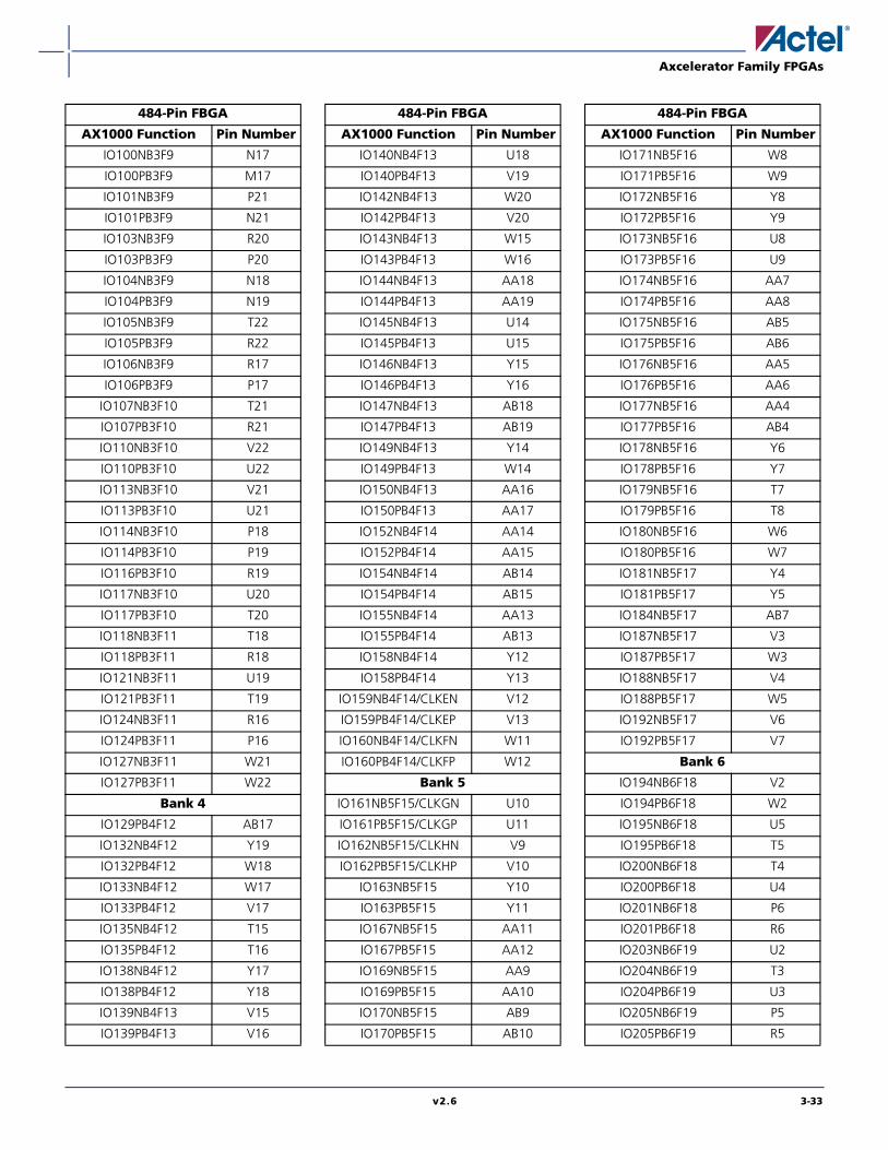
Axcelerator Family FPGAs
v2.6 3-33
IO100NB3F9 N17
IO100PB3F9 M17
IO101NB3F9 P21
IO101PB3F9 N21
IO103NB3F9 R20
IO103PB3F9 P20
IO104NB3F9 N18
IO104PB3F9 N19
IO105NB3F9 T22
IO105PB3F9 R22
IO106NB3F9 R17
IO106PB3F9 P17
IO107NB3F10 T21
IO107PB3F10 R21
IO110NB3F10 V22
IO110PB3F10 U22
IO113NB3F10 V21
IO113PB3F10 U21
IO114NB3F10 P18
IO114PB3F10 P19
IO116PB3F10 R19
IO117NB3F10 U20
IO117PB3F10 T20
IO118NB3F11 T18
IO118PB3F11 R18
IO121NB3F11 U19
IO121PB3F11 T19
IO124NB3F11 R16
IO124PB3F11 P16
IO127NB3F11 W21
IO127PB3F11 W22
Bank 4
IO129PB4F12 AB17
IO132NB4F12 Y19
IO132PB4F12 W18
IO133NB4F12 W17
IO133PB4F12 V17
IO135NB4F12 T15
IO135PB4F12 T16
IO138NB4F12 Y17
IO138PB4F12 Y18
IO139NB4F13 V15
IO139PB4F13 V16
484-Pin FBGA
AX1000 Function Pin Number
IO140NB4F13 U18
IO140PB4F13 V19
IO142NB4F13 W20
IO142PB4F13 V20
IO143NB4F13 W15
IO143PB4F13 W16
IO144NB4F13 AA18
IO144PB4F13 AA19
IO145NB4F13 U14
IO145PB4F13 U15
IO146NB4F13 Y15
IO146PB4F13 Y16
IO147NB4F13 AB18
IO147PB4F13 AB19
IO149NB4F13 Y14
IO149PB4F13 W14
IO150NB4F13 AA16
IO150PB4F13 AA17
IO152NB4F14 AA14
IO152PB4F14 AA15
IO154NB4F14 AB14
IO154PB4F14 AB15
IO155NB4F14 AA13
IO155PB4F14 AB13
IO158NB4F14 Y12
IO158PB4F14 Y13
IO159NB4F14/CLKEN V12
IO159PB4F14/CLKEP V13
IO160NB4F14/CLKFN W11
IO160PB4F14/CLKFP W12
Bank 5
IO161NB5F15/CLKGN U10
IO161PB5F15/CLKGP U11
IO162NB5F15/CLKHN V9
IO162PB5F15/CLKHP V10
IO163NB5F15 Y10
IO163PB5F15 Y11
IO167NB5F15 AA11
IO167PB5F15 AA12
IO169NB5F15 AA9
IO169PB5F15 AA10
IO170NB5F15 AB9
IO170PB5F15 AB10
484-Pin FBGA
AX1000 Function Pin Number
IO171NB5F16 W8
IO171PB5F16 W9
IO172NB5F16 Y8
IO172PB5F16 Y9
IO173NB5F16 U8
IO173PB5F16 U9
IO174NB5F16 AA7
IO174PB5F16 AA8
IO175NB5F16 AB5
IO175PB5F16 AB6
IO176NB5F16 AA5
IO176PB5F16 AA6
IO177NB5F16 AA4
IO177PB5F16 AB4
IO178NB5F16 Y6
IO178PB5F16 Y7
IO179NB5F16 T7
IO179PB5F16 T8
IO180NB5F16 W6
IO180PB5F16 W7
IO181NB5F17 Y4
IO181PB5F17 Y5
IO184NB5F17 AB7
IO187NB5F17 V3
IO187PB5F17 W3
IO188NB5F17 V4
IO188PB5F17 W5
IO192NB5F17 V6
IO192PB5F17 V7
Bank 6
IO194NB6F18 V2
IO194PB6F18 W2
IO195NB6F18 U5
IO195PB6F18 T5
IO200NB6F18 T4
IO200PB6F18 U4
IO201NB6F18 P6
IO201PB6F18 R6
IO203NB6F19 U2
IO204NB6F19 T3
IO204PB6F19 U3
IO205NB6F19 P5
IO205PB6F19 R5
484-Pin FBGA
AX1000 Function Pin Number

Axcelerator Family FPGAs
3-34 v2.6
IO208NB6F19 V1
IO208PB6F19 W1
IO209NB6F19 P7
IO209PB6F19 R7
IO212NB6F19 P4
IO212PB6F19 R4
IO214NB6F20 P3
IO214PB6F20 R3
IO215NB6F20 M6
IO215PB6F20 N6
IO216NB6F20 R2
IO216PB6F20 T2
IO217NB6F20 T1
IO217PB6F20 U1
IO219NB6F20 M5
IO219PB6F20 N5
IO220NB6F20 P1
IO220PB6F20 R1
IO221NB6F20 N2
IO221PB6F20 P2
IO222NB6F20 M3
IO222PB6F20 N3
IO223NB6F20 M7
IO223PB6F20 N7
IO224NB6F20 M4
IO224PB6F20 N4
Bank 7
IO225NB7F21 M2
IO225PB7F21 N1
IO226NB7F21 K2
IO226PB7F21 K1
IO228NB7F21 L3
IO228PB7F21 L2
IO229NB7F21 K5
IO229PB7F21 L5
IO230NB7F21 H1
IO230PB7F21 J1
IO231NB7F21 H2
IO231PB7F21 J2
IO232NB7F21 K4
IO232PB7F21 K3
IO233NB7F21 K6
IO233PB7F21 L6
484-Pin FBGA
AX1000 Function Pin Number
IO234NB7F21 F1
IO234PB7F21 G1
IO235NB7F21 F2
IO235PB7F21 G2
IO236NB7F22 H3
IO236PB7F22 J3
IO237NB7F22 K7
IO237PB7F22 L7
IO241NB7F22 H6
IO241PB7F22 J6
IO242NB7F22 H4
IO242PB7F22 J4
IO243NB7F22 H5
IO243PB7F22 J5
IO246NB7F22 F3
IO246PB7F22 G3
IO250NB7F23 F4
IO250PB7F23 G4
IO253NB7F23 G5
IO253PB7F23 G6
IO254NB7F23 D1
IO254PB7F23 E1
IO257NB7F23 F5
IO257PB7F23 E4
Dedicated I/O
VCCDA H7
GND A1
GND A11
GND A12
GND A2
GND A21
GND A22
GND AA1
GND AA2
GND AA21
GND AA22
GND AB1
GND AB11
GND AB12
GND AB2
GND AB21
GND AB22
GND B1
484-Pin FBGA
AX1000 Function Pin Number
GND B2
GND B21
GND B22
GND C20
GND C3
GND D19
GND D4
GND E18
GND E5
GND G18
GND H15
GND H8
GND J14
GND J9
GND K10
GND K11
GND K12
GND K13
GND L1
GND L10
GND L11
GND L12
GND L13
GND L22
GND M1
GND M10
GND M11
GND M12
GND M13
GND M22
GND N10
GND N11
GND N12
GND N13
GND P14
GND P9
GND R15
GND R8
GND U16
GND U6
GND V18
GND V5
GND W19
484-Pin FBGA
AX1000 Function Pin Number

Axcelerator Family FPGAs
v2.6 3-35
GND W4
GND Y20
GND Y3
GND/LP G7
PRA G11
PRB F11
PRC T12
PRD U12
TCK G8
TDI F9
TDO F7
TMS F6
TRST F8
VCCA G17
VCCA J10
VCCA J11
VCCA J12
VCCA J13
VCCA J7
VCCA K14
VCCA K9
VCCA L14
VCCA L9
VCCA M14
VCCA M9
VCCA N14
VCCA N9
VCCA P10
VCCA P11
VCCA P12
VCCA P13
VCCA T6
VCCA U17
VCCPLA F10
VCCPLB G9
VCCPLC D13
VCCPLD G13
VCCPLE U13
VCCPLF T14
VCCPLG W10
VCCPLH T10
VCCDA AB16
VCCDA AB8
484-Pin FBGA
AX1000 Function Pin Number
VCCDA C10
VCCDA C11
VCCDA C14
VCCDA D14
VCCDA D5
VCCDA F16
VCCDA G12
VCCDA L4
VCCDA M18
VCCDA T11
VCCDA T17
VCCDA U7
VCCDA V14
VCCDA V8
VCCIB0 A3
VCCIB0 B3
VCCIB0 H10
VCCIB0 H11
VCCIB0 H9
VCCIB1 A20
VCCIB1 B20
VCCIB1 H12
VCCIB1 H13
VCCIB1 H14
VCCIB2 C21
VCCIB2 C22
VCCIB2 J15
VCCIB2 K15
VCCIB2 L15
VCCIB3 M15
VCCIB3 N15
VCCIB3 P15
VCCIB3 Y21
VCCIB3 Y22
VCCIB4 AA20
VCCIB4 AB20
VCCIB4 R12
VCCIB4 R13
VCCIB4 R14
VCCIB5 AA3
VCCIB5 AB3
VCCIB5 R10
VCCIB5 R11
484-Pin FBGA
AX1000 Function Pin Number
VCCIB5 R9
VCCIB6 M8
VCCIB6 N8
VCCIB6 P8
VCCIB6 Y1
VCCIB6 Y2
VCCIB7 C1
VCCIB7 C2
VCCIB7 J8
VCCIB7 K8
VCCIB7 L8
VCOMPLA D10
VCOMPLB G10
VCOMPLC E12
VCOMPLD G14
VCOMPLE W13
VCOMPLF T13
VCOMPLG V11
VCOMPLH T9
VPUMP D17
484-Pin FBGA
AX1000 Function Pin Number

Axcelerator Family FPGAs
3-36 v2.6
676-Pin FBGA
NoteFor Package Manufacturing and Environmental information, visit Resource center athttp://www.actel.com/products/rescenter/package/index.html.
Figure 3-6 • 676-Pin FBGA (Bottom View)
A1 Ball Pad Corner
A
B
C
D
E
F
G
H
J
K
L
M
N
P
R
T
U
V
W
Y
AA
AB
AC
AD
AE
AF
1234567891011121314151617181920212223242526
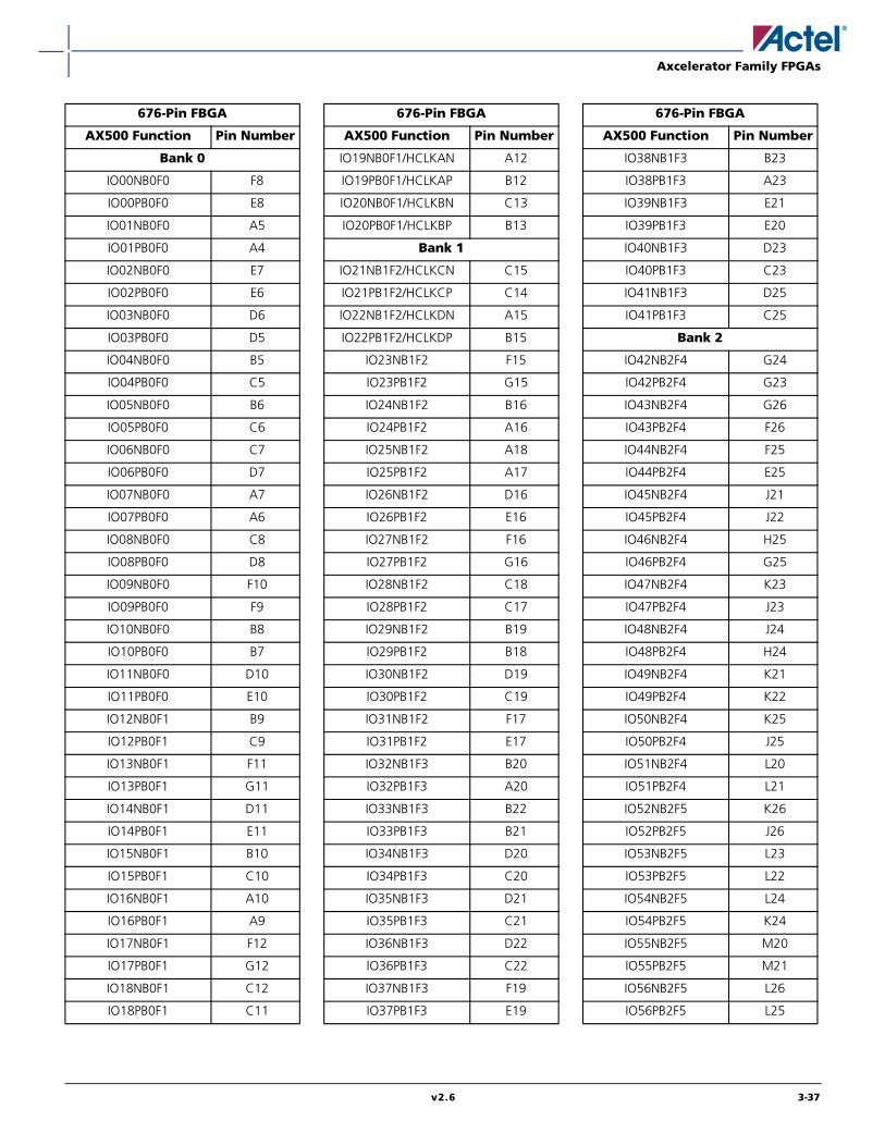
Axcelerator Family FPGAs
v2.6 3-37
676-Pin FBGA
AX500 Function Pin Number
Bank 0
IO00NB0F0 F8
IO00PB0F0 E8
IO01NB0F0 A5
IO01PB0F0 A4
IO02NB0F0 E7
IO02PB0F0 E6
IO03NB0F0 D6
IO03PB0F0 D5
IO04NB0F0 B5
IO04PB0F0 C5
IO05NB0F0 B6
IO05PB0F0 C6
IO06NB0F0 C7
IO06PB0F0 D7
IO07NB0F0 A7
IO07PB0F0 A6
IO08NB0F0 C8
IO08PB0F0 D8
IO09NB0F0 F10
IO09PB0F0 F9
IO10NB0F0 B8
IO10PB0F0 B7
IO11NB0F0 D10
IO11PB0F0 E10
IO12NB0F1 B9
IO12PB0F1 C9
IO13NB0F1 F11
IO13PB0F1 G11
IO14NB0F1 D11
IO14PB0F1 E11
IO15NB0F1 B10
IO15PB0F1 C10
IO16NB0F1 A10
IO16PB0F1 A9
IO17NB0F1 F12
IO17PB0F1 G12
IO18NB0F1 C12
IO18PB0F1 C11
IO19NB0F1/HCLKAN A12
IO19PB0F1/HCLKAP B12
IO20NB0F1/HCLKBN C13
IO20PB0F1/HCLKBP B13
Bank 1
IO21NB1F2/HCLKCN C15
IO21PB1F2/HCLKCP C14
IO22NB1F2/HCLKDN A15
IO22PB1F2/HCLKDP B15
IO23NB1F2 F15
IO23PB1F2 G15
IO24NB1F2 B16
IO24PB1F2 A16
IO25NB1F2 A18
IO25PB1F2 A17
IO26NB1F2 D16
IO26PB1F2 E16
IO27NB1F2 F16
IO27PB1F2 G16
IO28NB1F2 C18
IO28PB1F2 C17
IO29NB1F2 B19
IO29PB1F2 B18
IO30NB1F2 D19
IO30PB1F2 C19
IO31NB1F2 F17
IO31PB1F2 E17
IO32NB1F3 B20
IO32PB1F3 A20
IO33NB1F3 B22
IO33PB1F3 B21
IO34NB1F3 D20
IO34PB1F3 C20
IO35NB1F3 D21
IO35PB1F3 C21
IO36NB1F3 D22
IO36PB1F3 C22
IO37NB1F3 F19
IO37PB1F3 E19
676-Pin FBGA
AX500 Function Pin Number
IO38NB1F3 B23
IO38PB1F3 A23
IO39NB1F3 E21
IO39PB1F3 E20
IO40NB1F3 D23
IO40PB1F3 C23
IO41NB1F3 D25
IO41PB1F3 C25
Bank 2
IO42NB2F4 G24
IO42PB2F4 G23
IO43NB2F4 G26
IO43PB2F4 F26
IO44NB2F4 F25
IO44PB2F4 E25
IO45NB2F4 J21
IO45PB2F4 J22
IO46NB2F4 H25
IO46PB2F4 G25
IO47NB2F4 K23
IO47PB2F4 J23
IO48NB2F4 J24
IO48PB2F4 H24
IO49NB2F4 K21
IO49PB2F4 K22
IO50NB2F4 K25
IO50PB2F4 J25
IO51NB2F4 L20
IO51PB2F4 L21
IO52NB2F5 K26
IO52PB2F5 J26
IO53NB2F5 L23
IO53PB2F5 L22
IO54NB2F5 L24
IO54PB2F5 K24
IO55NB2F5 M20
IO55PB2F5 M21
IO56NB2F5 L26
IO56PB2F5 L25
676-Pin FBGA
AX500 Function Pin Number

Axcelerator Family FPGAs
3-38 v2.6
IO57NB2F5 M23
IO57PB2F5 M22
IO58NB2F5 M26
IO58PB2F5 M25
IO59NB2F5 N22
IO59PB2F5 N23
IO60NB2F5 N24
IO60PB2F5 M24
IO61NB2F5 N20
IO61PB2F5 N21
IO62NB2F5 P25
IO62PB2F5 N25
Bank 3
IO63NB3F6 T26
IO63PB3F6 R26
IO64NB3F6 R24
IO64PB3F6 P24
IO65NB3F6 P20
IO65PB3F6 P21
IO66NB3F6 T25
IO66PB3F6 R25
IO67NB3F6 T23
IO67PB3F6 R23
IO68NB3F6 V26
IO68PB3F6 U26
IO69NB3F6 V25
IO69PB3F6 U25
IO70NB3F6 Y25
IO70PB3F6 W25
IO71NB3F6 W24
IO71PB3F6 V24
IO72NB3F6 V23
IO72PB3F6 U23
IO73NB3F6 T21
IO73PB3F6 T20
IO74NB3F7 AA26
IO74PB3F7 Y26
IO75NB3F7 AA24
IO75PB3F7 Y24
676-Pin FBGA
AX500 Function Pin Number
IO76NB3F7 Y23
IO76PB3F7 W23
IO77NB3F7 V21
IO77PB3F7 U21
IO78NB3F7 AB25
IO78PB3F7 AA25
IO79NB3F7 AC26
IO79PB3F7 AB26
IO80NB3F7 AC24
IO80PB3F7 AB24
IO81NB3F7 AB23
IO81PB3F7 AA23
IO82NB3F7 AA22
IO82PB3F7 Y22
IO83NB3F7 AE26
IO83PB3F7 AD26
Bank 4
IO84NB4F8 AB21
IO84PB4F8 AA21
IO85NB4F8 AE23
IO85PB4F8 AE24
IO86NB4F8 AC21
IO86PB4F8 AC22
IO87NB4F8 AF22
IO87PB4F8 AF23
IO88NB4F8 AD22
IO88PB4F8 AD23
IO89NB4F8 AC19
IO89PB4F8 AC20
IO90NB4F8 AE21
IO90PB4F8 AE22
IO91NB4F8 AA17
IO91PB4F8 AA18
IO92NB4F8 AD20
IO92PB4F8 AD21
IO93NB4F8 AF20
IO93PB4F8 AF21
IO94NB4F9 AE19
IO94PB4F9 AE20
676-Pin FBGA
AX500 Function Pin Number
IO95NB4F9 AC17
IO95PB4F9 AC18
IO96NB4F9 AD18
IO96PB4F9 AD19
IO97NB4F9 AA16
IO97PB4F9 Y16
IO98NB4F9 AE17
IO98PB4F9 AE18
IO99NB4F9 AC16
IO99PB4F9 AB16
IO100NB4F9 AF17
IO100PB4F9 AF18
IO101NB4F9 AA15
IO101PB4F9 Y15
IO102NB4F9 AC15
IO102PB4F9 AB15
IO103NB4F9/CLKEN AE16
IO103PB4F9/CLKEP AF16
IO104NB4F9/CLKFN AE14
IO104PB4F9/CLKFP AE15
Bank 5
IO105NB5F10/CLKGN AE12
IO105PB5F10/CLKGP AE13
IO106NB5F10/CLKHN AE11
IO106PB5F10/CLKHP AF11
IO107NB5F10 Y12
IO107PB5F10 AA13
IO108NB5F10 AC12
IO108PB5F10 AB12
IO109NB5F10 AC10
IO109PB5F10 AC11
IO110NB5F10 AF9
IO110PB5F10 AF10
IO111NB5F10 Y11
IO111PB5F10 AA12
IO112NB5F10 AE9
IO112PB5F10 AE10
IO113NB5F10 AC9
IO113PB5F10 AD9
676-Pin FBGA
AX500 Function Pin Number

Axcelerator Family FPGAs
v2.6 3-39
IO114NB5F11 AF6
IO114PB5F11 AF7
IO115NB5F11 AA10
IO115PB5F11 AB10
IO116NB5F11 AE7
IO116PB5F11 AE8
IO117NB5F11 AD7
IO117PB5F11 AD8
IO118NB5F11 AC7
IO118PB5F11 AC8
IO119NB5F11 AD6
IO119PB5F11 AE6
IO120NB5F11 AE5
IO120PB5F11 AF5
IO121NB5F11 AF4
IO121PB5F11 AE4
IO122NB5F11 AC5
IO122PB5F11 AC6
IO123NB5F11 AD4
IO123PB5F11 AD5
IO124NB5F11 AB6
IO124PB5F11 AB7
IO125NB5F11 AE3
IO125PB5F11 AF3
Bank 6
IO126NB6F12 AB3
IO126PB6F12 AC3
IO127NB6F12 AA2
IO127PB6F12 AB2
IO128NB6F12 AC2
IO128PB6F12 AD2
IO129NB6F12 Y1
IO129PB6F12 AA1
IO130NB6F12 Y3
IO130PB6F12 AA3
IO131NB6F12 U6
IO131PB6F12 V6
IO132NB6F12 W2
IO132PB6F12 Y2
676-Pin FBGA
AX500 Function Pin Number
IO133NB6F12 V4
IO133PB6F12 W4
IO134NB6F12 V3
IO134PB6F12 W3
IO135NB6F12 V1
IO135PB6F12 V2
IO136NB6F13 U4
IO136PB6F13 U5
IO137NB6F13 T6
IO137PB6F13 T7
IO138NB6F13 T5
IO138PB6F13 T4
IO139NB6F13 R6
IO139PB6F13 R7
IO140NB6F13 T3
IO140PB6F13 U3
IO141NB6F13 U1
IO141PB6F13 U2
IO142NB6F13 R2
IO142PB6F13 T2
IO143NB6F13 P3
IO143PB6F13 R3
IO144NB6F13 P5
IO144PB6F13 P4
IO145NB6F13 P6
IO145PB6F13 P7
IO146NB6F13 R1
IO146PB6F13 T1
Bank 7
IO147NB7F14 N6
IO147PB7F14 N7
IO148NB7F14 N5
IO148PB7F14 N4
IO149NB7F14 N2
IO149PB7F14 N3
IO150NB7F14 L1
IO150PB7F14 M1
IO151NB7F14 M2
IO151PB7F14 M3
676-Pin FBGA
AX500 Function Pin Number
IO152NB7F14 M5
IO152PB7F14 M4
IO153NB7F14 M7
IO153PB7F14 M6
IO154NB7F14 K2
IO154PB7F14 L2
IO155NB7F14 K3
IO155PB7F14 L3
IO156NB7F14 L5
IO156PB7F14 L4
IO157NB7F14 L6
IO157PB7F14 L7
IO158NB7F15 J1
IO158PB7F15 K1
IO159NB7F15 J4
IO159PB7F15 K4
IO160NB7F15 H2
IO160PB7F15 J2
IO161NB7F15 K6
IO161PB7F15 K5
IO162NB7F15 H3
IO162PB7F15 J3
IO163NB7F15 G2
IO163PB7F15 G1
IO164NB7F15 G4
IO164PB7F15 H4
IO165NB7F15 F3
IO165PB7F15 G3
IO166NB7F15 E2
IO166PB7F15 F2
IO167NB7F15 F5
IO167PB7F15 G5
Dedicated I/O
GND A1
GND A13
GND A14
GND A19
GND A26
GND A8
676-Pin FBGA
AX500 Function Pin Number
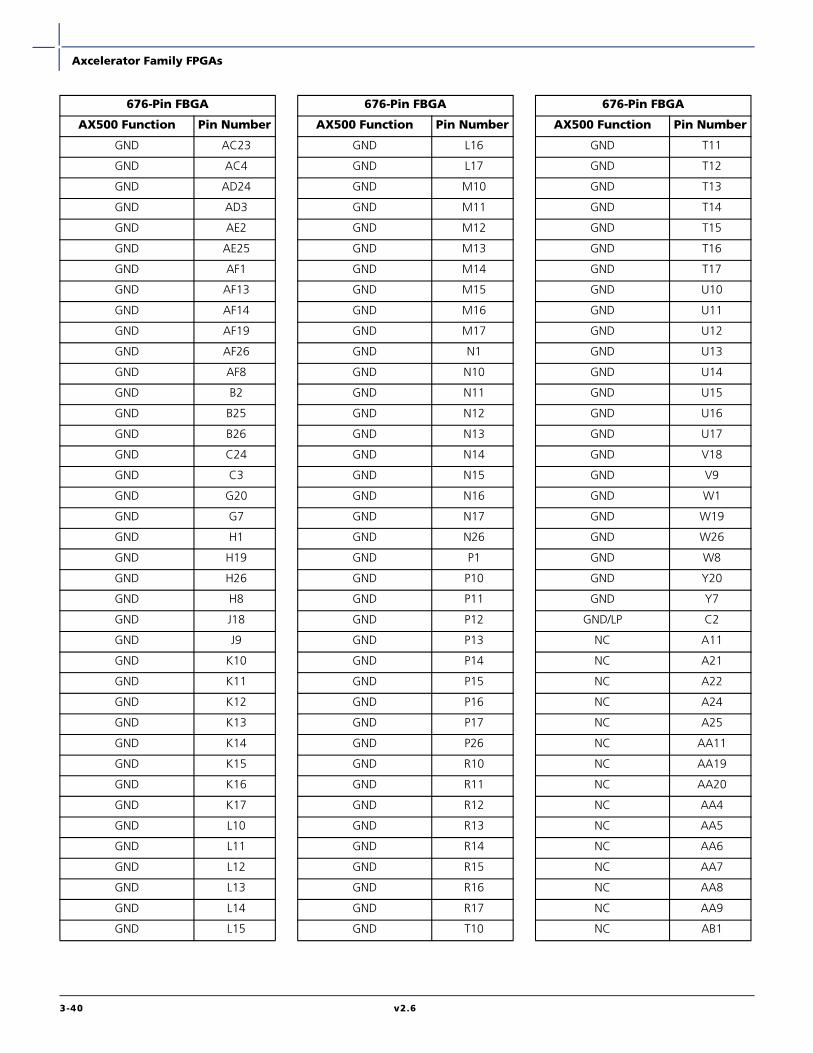
Axcelerator Family FPGAs
3-40 v2.6
GND AC23
GND AC4
GND AD24
GND AD3
GND AE2
GND AE25
GND AF1
GND AF13
GND AF14
GND AF19
GND AF26
GND AF8
GND B2
GND B25
GND B26
GND C24
GND C3
GND G20
GND G7
GND H1
GND H19
GND H26
GND H8
GND J18
GND J9
GND K10
GND K11
GND K12
GND K13
GND K14
GND K15
GND K16
GND K17
GND L10
GND L11
GND L12
GND L13
GND L14
GND L15
676-Pin FBGA
AX500 Function Pin Number
GND L16
GND L17
GND M10
GND M11
GND M12
GND M13
GND M14
GND M15
GND M16
GND M17
GND N1
GND N10
GND N11
GND N12
GND N13
GND N14
GND N15
GND N16
GND N17
GND N26
GND P1
GND P10
GND P11
GND P12
GND P13
GND P14
GND P15
GND P16
GND P17
GND P26
GND R10
GND R11
GND R12
GND R13
GND R14
GND R15
GND R16
GND R17
GND T10
676-Pin FBGA
AX500 Function Pin Number
GND T11
GND T12
GND T13
GND T14
GND T15
GND T16
GND T17
GND U10
GND U11
GND U12
GND U13
GND U14
GND U15
GND U16
GND U17
GND V18
GND V9
GND W1
GND W19
GND W26
GND W8
GND Y20
GND Y7
GND/LP C2
NC A11
NC A21
NC A22
NC A24
NC A25
NC AA11
NC AA19
NC AA20
NC AA4
NC AA5
NC AA6
NC AA7
NC AA8
NC AA9
NC AB1
676-Pin FBGA
AX500 Function Pin Number

Axcelerator Family FPGAs
v2.6 3-41
NC AB11
NC AB17
NC AB18
NC AB19
NC AB20
NC AB8
NC AB9
NC AC1
NC AC13
NC AC14
NC AC25
NC AD1
NC AD11
NC AD16
NC AD25
NC AE1
NC AF2
NC AF25
NC B11
NC B24
NC B4
NC C16
NC C4
NC D1
NC D13
NC D14
NC D17
NC D18
NC D2
NC D26
NC D3
NC D9
NC E1
NC E18
NC E23
NC E24
NC E26
NC E3
NC E4
676-Pin FBGA
AX500 Function Pin Number
NC E9
NC F1
NC F18
NC F20
NC F21
NC F22
NC F23
NC F24
NC F4
NC F6
NC F7
NC G21
NC G22
NC H21
NC H22
NC H23
NC H5
NC H6
NC J5
NC J6
NC P22
NC R20
NC R21
NC R22
NC R4
NC R5
NC T22
NC T24
NC U22
NC U24
NC V22
NC V5
NC W21
NC W22
NC W5
NC W6
NC Y21
NC Y4
NC Y5
676-Pin FBGA
AX500 Function Pin Number
NC Y6
PRA E13
PRB B14
PRC Y14
PRD AD14
TCK E5
TDI B3
TDO G6
TMS D4
TRST A2
VCCA AB4
VCCA AF24
VCCA C1
VCCA C26
VCCA J10
VCCA J11
VCCA J12
VCCA J13
VCCA J14
VCCA J15
VCCA J16
VCCA J17
VCCA K18
VCCA K9
VCCA L18
VCCA L9
VCCA M18
VCCA M9
VCCA N18
VCCA N9
VCCA P18
VCCA P9
VCCA R18
VCCA R9
VCCA T18
VCCA T9
VCCA U18
VCCA U9
VCCA V10
676-Pin FBGA
AX500 Function Pin Number

Axcelerator Family FPGAs
3-42 v2.6
VCCA V11
VCCA V12
VCCA V13
VCCA V14
VCCA V15
VCCA V16
VCCA V17
VCCDA A3
VCCDA AB22
VCCDA AB5
VCCDA AD10
VCCDA AD13
VCCDA AD17
VCCDA B1
VCCDA B17
VCCDA D24
VCCDA E14
VCCDA P2
VCCDA P23
VCCIB0 G10
VCCIB0 G8
VCCIB0 G9
VCCIB0 H10
VCCIB0 H11
VCCIB0 H12
VCCIB0 H13
VCCIB0 H9
VCCIB1 G17
VCCIB1 G18
VCCIB1 G19
VCCIB1 H14
VCCIB1 H15
VCCIB1 H16
VCCIB1 H17
VCCIB1 H18
VCCIB2 H20
VCCIB2 J19
VCCIB2 J20
VCCIB2 K19
676-Pin FBGA
AX500 Function Pin Number
VCCIB2 K20
VCCIB2 L19
VCCIB2 M19
VCCIB2 N19
VCCIB3 P19
VCCIB3 R19
VCCIB3 T19
VCCIB3 U19
VCCIB3 U20
VCCIB3 V19
VCCIB3 V20
VCCIB3 W20
VCCIB4 W14
VCCIB4 W15
VCCIB4 W16
VCCIB4 W17
VCCIB4 W18
VCCIB4 Y17
VCCIB4 Y18
VCCIB4 Y19
VCCIB5 W10
VCCIB5 W11
VCCIB5 W12
VCCIB5 W13
VCCIB5 W9
VCCIB5 Y10
VCCIB5 Y8
VCCIB5 Y9
VCCIB6 P8
VCCIB6 R8
VCCIB6 T8
VCCIB6 U7
VCCIB6 U8
VCCIB6 V7
VCCIB6 V8
VCCIB6 W7
VCCIB7 H7
VCCIB7 J7
VCCIB7 J8
676-Pin FBGA
AX500 Function Pin Number
VCCIB7 K7
VCCIB7 K8
VCCIB7 L8
VCCIB7 M8
VCCIB7 N8
VCCPLA E12
VCCPLB F13
VCCPLC E15
VCCPLD G14
VCCPLE AF15
VCCPLF AA14
VCCPLG AF12
VCCPLH AB13
VCOMPLA D12
VCOMPLB G13
VCOMPLC D15
VCOMPLD F14
VCOMPLE AD15
VCOMPLF AB14
VCOMPLG AD12
VCOMPLH Y13
VPUMP E22
676-Pin FBGA
AX500 Function Pin Number

Axcelerator Family FPGAs
v2.6 3-43
676-Pin FBGA
AX1000 Function Pin Number
Bank 0
IO00NB0F0 B4
IO00PB0F0 C4
IO02NB0F0 E7
IO02PB0F0 E6
IO03NB0F0 D6
IO03PB0F0 D5
IO04NB0F0 B5
IO04PB0F0 C5
IO05NB0F0 A5
IO05PB0F0 A4
IO06NB0F0 F7
IO06PB0F0 F6
IO07NB0F0 B6
IO07PB0F0 C6
IO08NB0F0 C7
IO08PB0F0 D7
IO10NB0F0 F8
IO10PB0F0 E8
IO11NB0F0 A7
IO11PB0F0 A6
IO12NB0F1 C8
IO12PB0F1 D8
IO13NB0F1 B8
IO13PB0F1 B7
IO14NB0F1 D9
IO14PB0F1 E9
IO16NB0F1 F10
IO16PB0F1 F9
IO18NB0F1 B9
IO18PB0F1 C9
IO19NB0F1 A10
IO19PB0F1 A9
IO20NB0F1 D10
IO20PB0F1 E10
IO21NB0F1 B10
IO21PB0F1 C10
IO22NB0F2 F11
IO22PB0F2 G11
IO24NB0F2 D11
IO24PB0F2 E11
IO26NB0F2 C12
IO26PB0F2 C11
IO28NB0F2 F12
IO28PB0F2 G12
IO30NB0F2/HCLKAN A12
IO30PB0F2/HCLKAP B12
IO31NB0F2/HCLKBN C13
IO31PB0F2/HCLKBP B13
Bank 1
IO32NB1F3/HCLKCN C15
IO32PB1F3/HCLKCP C14
IO33NB1F3/HCLKDN A15
IO33PB1F3/HCLKDP B15
IO35NB1F3 B16
IO35PB1F3 A16
IO36NB1F3 F15
IO36PB1F3 G15
IO38NB1F3 F16
IO38PB1F3 G16
IO40NB1F3 A18
IO40PB1F3 A17
IO41NB1F4 C18
IO41PB1F4 C17
IO42NB1F4 D16
IO42PB1F4 E16
IO44NB1F4 D18
IO44PB1F4 D17
IO45NB1F4 B19
IO45PB1F4 B18
IO46NB1F4 B20
IO46PB1F4 A20
IO48NB1F4 F17
IO48PB1F4 E17
IO49NB1F4 A22
IO49PB1F4 A21
IO50NB1F4 E18
IO50PB1F4 F18
676-Pin FBGA
AX1000 Function Pin Number
IO51NB1F4 D19
IO51PB1F4 C19
IO52NB1F4 D20
IO52PB1F4 C20
IO54NB1F5 B22
IO54PB1F5 B21
IO55NB1F5 D21
IO55PB1F5 C21
IO56NB1F5 F19
IO56PB1F5 E19
IO57NB1F5 B23
IO57PB1F5 A23
IO58NB1F5 D22
IO58PB1F5 C22
IO59NB1F5 B24
IO59PB1F5 A24
IO60NB1F5 E21
IO60PB1F5 E20
IO62NB1F5 D23
IO62PB1F5 C23
IO63NB1F5 F21
IO63PB1F5 F20
Bank 2
IO64NB2F6 H21
IO64PB2F6 G21
IO65NB2F6 G22
IO65PB2F6 F22
IO66NB2F6 F24
IO66PB2F6 F23
IO67NB2F6 E24
IO67PB2F6 E23
IO68NB2F6 H23
IO68PB2F6 H22
IO69NB2F6 D25
IO69PB2F6 C25
IO70NB2F6 G24
IO70PB2F6 G23
IO71NB2F6 F25
IO71PB2F6 E25
676-Pin FBGA
AX1000 Function Pin Number

Axcelerator Family FPGAs
3-44 v2.6
IO72NB2F6 G26
IO72PB2F6 F26
IO73NB2F6 E26
IO73PB2F6 D26
IO74NB2F7 J21
IO74PB2F7 J22
IO75NB2F7 J24
IO75PB2F7 H24
IO76NB2F7 K23
IO76PB2F7 J23
IO77NB2F7 H25
IO77PB2F7 G25
IO78NB2F7 K25
IO78PB2F7 J25
IO80NB2F7 K21
IO80PB2F7 K22
IO81NB2F7 K26
IO81PB2F7 J26
IO82NB2F7 L24
IO82PB2F7 K24
IO83NB2F7 L23
IO83PB2F7 L22
IO84NB2F7 L20
IO84PB2F7 L21
IO86NB2F8 L26
IO86PB2F8 L25
IO88NB2F8 M23
IO88PB2F8 M22
IO89NB2F8 M26
IO89PB2F8 M25
IO90NB2F8 M20
IO90PB2F8 M21
IO91NB2F8 N24
IO91PB2F8 M24
IO92NB2F8 N22
IO92PB2F8 N23
IO94NB2F8 N20
IO94PB2F8 N21
IO95NB2F8 P25
676-Pin FBGA
AX1000 Function Pin Number
IO95PB2F8 N25
Bank 3
IO98NB3F9 P20
IO98PB3F9 P21
IO99NB3F9 R24
IO99PB3F9 P24
IO100NB3F9 R22
IO100PB3F9 P22
IO101NB3F9 T26
IO101PB3F9 R26
IO102NB3F9 R21
IO102PB3F9 R20
IO103NB3F9 T25
IO103PB3F9 R25
IO105NB3F9 V26
IO105PB3F9 U26
IO106NB3F9 T23
IO106PB3F9 R23
IO107NB3F10 U24
IO107PB3F10 T24
IO108NB3F10 U22
IO108PB3F10 T22
IO109NB3F10 V25
IO109PB3F10 U25
IO110NB3F10 T21
IO110PB3F10 T20
IO112NB3F10 V23
IO112PB3F10 U23
IO113NB3F10 Y25
IO113PB3F10 W25
IO114NB3F10 V21
IO114PB3F10 U21
IO115NB3F10 W24
IO115PB3F10 V24
IO116NB3F10 AA26
IO116PB3F10 Y26
IO118NB3F11 AC26
IO118PB3F11 AB26
IO119NB3F11 AB25
676-Pin FBGA
AX1000 Function Pin Number
IO119PB3F11 AA25
IO120NB3F11 W22
IO120PB3F11 V22
IO121NB3F11 Y23
IO121PB3F11 W23
IO122NB3F11 AA24
IO122PB3F11 Y24
IO123NB3F11 AE26
IO123PB3F11 AD26
IO124NB3F11 Y21
IO124PB3F11 W21
IO125NB3F11 AD25
IO125PB3F11 AC25
IO126NB3F11 AB23
IO126PB3F11 AA23
IO127NB3F11 AC24
IO127PB3F11 AB24
IO128NB3F11 AA22
IO128PB3F11 Y22
Bank 4
IO129NB4F12 AB21
IO129PB4F12 AA21
IO131NB4F12 AD22
IO131PB4F12 AD23
IO132NB4F12 AE23
IO132PB4F12 AE24
IO133NB4F12 AB20
IO133PB4F12 AA20
IO134NB4F12 AC21
IO134PB4F12 AC22
IO135NB4F12 AF22
IO135PB4F12 AF23
IO137NB4F12 AB19
IO137PB4F12 AA19
IO139NB4F13 AC19
IO139PB4F13 AC20
IO140NB4F13 AE21
IO140PB4F13 AE22
IO141NB4F13 AD20
676-Pin FBGA
AX1000 Function Pin Number
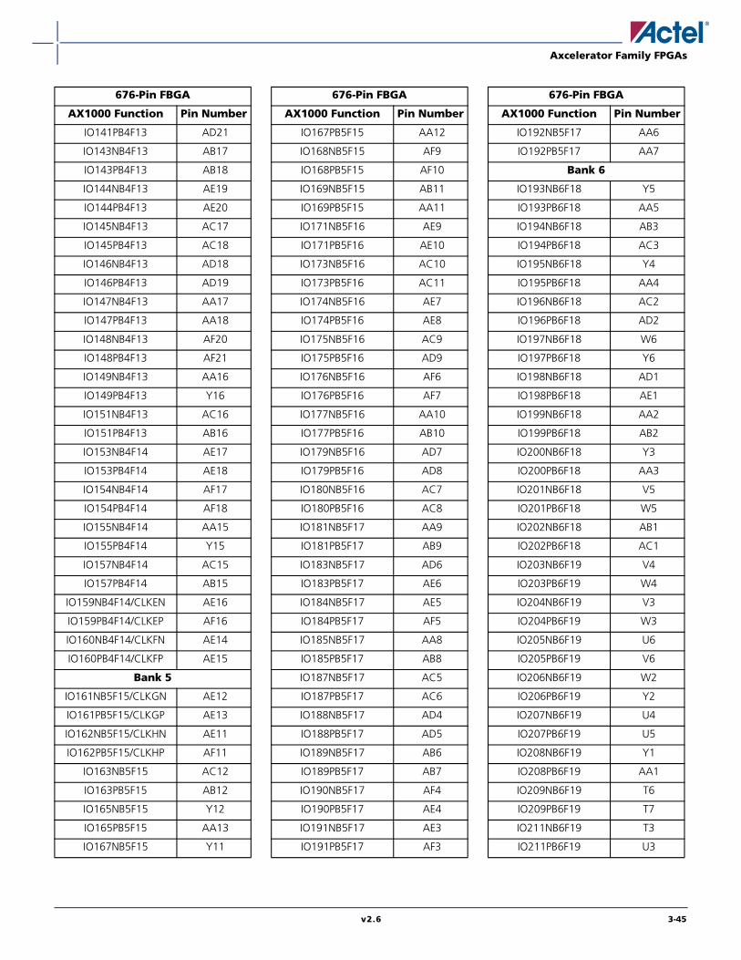
Axcelerator Family FPGAs
v2.6 3-45
IO141PB4F13 AD21
IO143NB4F13 AB17
IO143PB4F13 AB18
IO144NB4F13 AE19
IO144PB4F13 AE20
IO145NB4F13 AC17
IO145PB4F13 AC18
IO146NB4F13 AD18
IO146PB4F13 AD19
IO147NB4F13 AA17
IO147PB4F13 AA18
IO148NB4F13 AF20
IO148PB4F13 AF21
IO149NB4F13 AA16
IO149PB4F13 Y16
IO151NB4F13 AC16
IO151PB4F13 AB16
IO153NB4F14 AE17
IO153PB4F14 AE18
IO154NB4F14 AF17
IO154PB4F14 AF18
IO155NB4F14 AA15
IO155PB4F14 Y15
IO157NB4F14 AC15
IO157PB4F14 AB15
IO159NB4F14/CLKEN AE16
IO159PB4F14/CLKEP AF16
IO160NB4F14/CLKFN AE14
IO160PB4F14/CLKFP AE15
Bank 5
IO161NB5F15/CLKGN AE12
IO161PB5F15/CLKGP AE13
IO162NB5F15/CLKHN AE11
IO162PB5F15/CLKHP AF11
IO163NB5F15 AC12
IO163PB5F15 AB12
IO165NB5F15 Y12
IO165PB5F15 AA13
IO167NB5F15 Y11
676-Pin FBGA
AX1000 Function Pin Number
IO167PB5F15 AA12
IO168NB5F15 AF9
IO168PB5F15 AF10
IO169NB5F15 AB11
IO169PB5F15 AA11
IO171NB5F16 AE9
IO171PB5F16 AE10
IO173NB5F16 AC10
IO173PB5F16 AC11
IO174NB5F16 AE7
IO174PB5F16 AE8
IO175NB5F16 AC9
IO175PB5F16 AD9
IO176NB5F16 AF6
IO176PB5F16 AF7
IO177NB5F16 AA10
IO177PB5F16 AB10
IO179NB5F16 AD7
IO179PB5F16 AD8
IO180NB5F16 AC7
IO180PB5F16 AC8
IO181NB5F17 AA9
IO181PB5F17 AB9
IO183NB5F17 AD6
IO183PB5F17 AE6
IO184NB5F17 AE5
IO184PB5F17 AF5
IO185NB5F17 AA8
IO185PB5F17 AB8
IO187NB5F17 AC5
IO187PB5F17 AC6
IO188NB5F17 AD4
IO188PB5F17 AD5
IO189NB5F17 AB6
IO189PB5F17 AB7
IO190NB5F17 AF4
IO190PB5F17 AE4
IO191NB5F17 AE3
IO191PB5F17 AF3
676-Pin FBGA
AX1000 Function Pin Number
IO192NB5F17 AA6
IO192PB5F17 AA7
Bank 6
IO193NB6F18 Y5
IO193PB6F18 AA5
IO194NB6F18 AB3
IO194PB6F18 AC3
IO195NB6F18 Y4
IO195PB6F18 AA4
IO196NB6F18 AC2
IO196PB6F18 AD2
IO197NB6F18 W6
IO197PB6F18 Y6
IO198NB6F18 AD1
IO198PB6F18 AE1
IO199NB6F18 AA2
IO199PB6F18 AB2
IO200NB6F18 Y3
IO200PB6F18 AA3
IO201NB6F18 V5
IO201PB6F18 W5
IO202NB6F18 AB1
IO202PB6F18 AC1
IO203NB6F19 V4
IO203PB6F19 W4
IO204NB6F19 V3
IO204PB6F19 W3
IO205NB6F19 U6
IO205PB6F19 V6
IO206NB6F19 W2
IO206PB6F19 Y2
IO207NB6F19 U4
IO207PB6F19 U5
IO208NB6F19 Y1
IO208PB6F19 AA1
IO209NB6F19 T6
IO209PB6F19 T7
IO211NB6F19 T3
IO211PB6F19 U3
676-Pin FBGA
AX1000 Function Pin Number

Axcelerator Family FPGAs
3-46 v2.6
IO212NB6F19 V1
IO212PB6F19 V2
IO213NB6F19 T5
IO213PB6F19 T4
IO214NB6F20 U1
IO214PB6F20 U2
IO215NB6F20 R6
IO215PB6F20 R7
IO217NB6F20 R5
IO217PB6F20 R4
IO218NB6F20 R2
IO218PB6F20 T2
IO219NB6F20 P3
IO219PB6F20 R3
IO220NB6F20 R1
IO220PB6F20 T1
IO221NB6F20 P6
IO221PB6F20 P7
IO223NB6F20 P5
IO223PB6F20 P4
Bank 7
IO225NB7F21 N5
IO225PB7F21 N4
IO226NB7F21 N2
IO226PB7F21 N3
IO227NB7F21 N6
IO227PB7F21 N7
IO229NB7F21 M7
IO229PB7F21 M6
IO231NB7F21 M5
IO231PB7F21 M4
IO232NB7F21 L1
IO232PB7F21 M1
IO233NB7F21 M2
IO233PB7F21 M3
IO235NB7F21 K2
IO235PB7F21 L2
IO236NB7F22 L5
IO236PB7F22 L4
676-Pin FBGA
AX1000 Function Pin Number
IO237NB7F22 L6
IO237PB7F22 L7
IO238NB7F22 K3
IO238PB7F22 L3
IO240NB7F22 J1
IO240PB7F22 K1
IO241NB7F22 K6
IO241PB7F22 K5
IO242NB7F22 H2
IO242PB7F22 J2
IO243NB7F22 J4
IO243PB7F22 K4
IO244NB7F22 H3
IO244PB7F22 J3
IO245NB7F22 G2
IO245PB7F22 G1
IO247NB7F23 J6
IO247PB7F23 J5
IO248NB7F23 E1
IO248PB7F23 F1
IO249NB7F23 E2
IO249PB7F23 F2
IO250NB7F23 G4
IO250PB7F23 H4
IO251NB7F23 F3
IO251PB7F23 G3
IO253NB7F23 H6
IO253PB7F23 H5
IO254NB7F23 D2
IO254PB7F23 D1
IO255NB7F23 E4
IO255PB7F23 F4
IO256NB7F23 D3
IO256PB7F23 E3
IO257NB7F23 F5
IO257PB7F23 G5
Dedicated I/O
GND A1
GND A13
676-Pin FBGA
AX1000 Function Pin Number
GND A14
GND A19
GND A26
GND A8
GND AC23
GND AC4
GND AD24
GND AD3
GND AE2
GND AE25
GND AF1
GND AF13
GND AF14
GND AF19
GND AF26
GND AF8
GND B2
GND B25
GND B26
GND C24
GND C3
GND G20
GND G7
GND H1
GND H19
GND H26
GND H8
GND J18
GND J9
GND K10
GND K11
GND K12
GND K13
GND K14
GND K15
GND K16
GND K17
GND L10
GND L11
676-Pin FBGA
AX1000 Function Pin Number
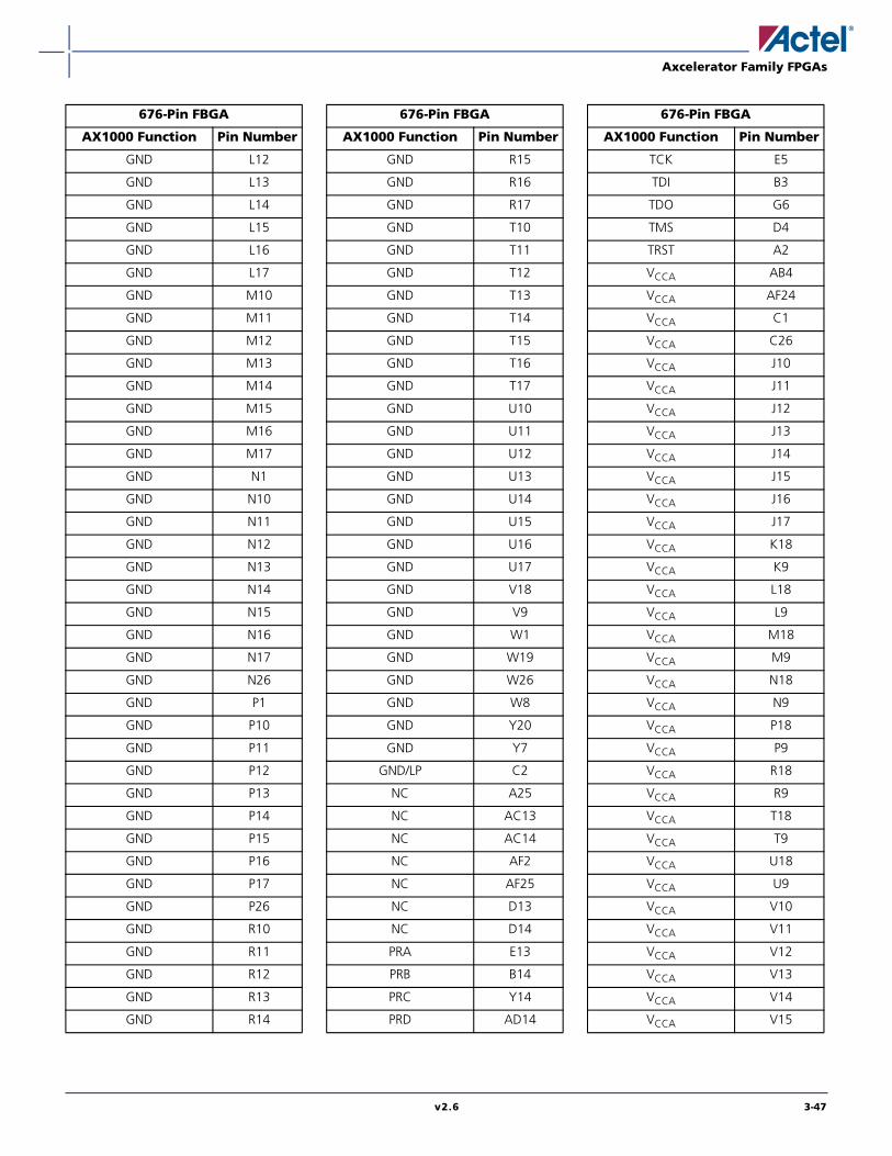
Axcelerator Family FPGAs
v2.6 3-47
GND L12
GND L13
GND L14
GND L15
GND L16
GND L17
GND M10
GND M11
GND M12
GND M13
GND M14
GND M15
GND M16
GND M17
GND N1
GND N10
GND N11
GND N12
GND N13
GND N14
GND N15
GND N16
GND N17
GND N26
GND P1
GND P10
GND P11
GND P12
GND P13
GND P14
GND P15
GND P16
GND P17
GND P26
GND R10
GND R11
GND R12
GND R13
GND R14
676-Pin FBGA
AX1000 Function Pin Number
GND R15
GND R16
GND R17
GND T10
GND T11
GND T12
GND T13
GND T14
GND T15
GND T16
GND T17
GND U10
GND U11
GND U12
GND U13
GND U14
GND U15
GND U16
GND U17
GND V18
GND V9
GND W1
GND W19
GND W26
GND W8
GND Y20
GND Y7
GND/LP C2
NC A25
NC AC13
NC AC14
NC AF2
NC AF25
NC D13
NC D14
PRA E13
PRB B14
PRC Y14
PRD AD14
676-Pin FBGA
AX1000 Function Pin Number
TCK E5
TDI B3
TDO G6
TMS D4
TRST A2
VCCA AB4
VCCA AF24
VCCA C1
VCCA C26
VCCA J10
VCCA J11
VCCA J12
VCCA J13
VCCA J14
VCCA J15
VCCA J16
VCCA J17
VCCA K18
VCCA K9
VCCA L18
VCCA L9
VCCA M18
VCCA M9
VCCA N18
VCCA N9
VCCA P18
VCCA P9
VCCA R18
VCCA R9
VCCA T18
VCCA T9
VCCA U18
VCCA U9
VCCA V10
VCCA V11
VCCA V12
VCCA V13
VCCA V14
VCCA V15
676-Pin FBGA
AX1000 Function Pin Number

Axcelerator Family FPGAs
3-48 v2.6
VCCA V16
VCCA V17
VCCPLA E12
VCCPLB F13
VCCPLC E15
VCCPLD G14
VCCPLE AF15
VCCPLF AA14
VCCPLG AF12
VCCPLH AB13
VCCDA A11
VCCDA A3
VCCDA AB22
VCCDA AB5
VCCDA AD10
VCCDA AD11
VCCDA AD13
VCCDA AD16
VCCDA AD17
VCCDA B1
VCCDA B11
VCCDA B17
VCCDA C16
VCCDA D24
VCCDA E14
VCCDA P2
VCCDA P23
VCCIB0 G10
VCCIB0 G8
VCCIB0 G9
VCCIB0 H10
VCCIB0 H11
VCCIB0 H12
VCCIB0 H13
VCCIB0 H9
VCCIB1 G17
VCCIB1 G18
VCCIB1 G19
VCCIB1 H14
676-Pin FBGA
AX1000 Function Pin Number
VCCIB1 H15
VCCIB1 H16
VCCIB1 H17
VCCIB1 H18
VCCIB2 H20
VCCIB2 J19
VCCIB2 J20
VCCIB2 K19
VCCIB2 K20
VCCIB2 L19
VCCIB2 M19
VCCIB2 N19
VCCIB3 P19
VCCIB3 R19
VCCIB3 T19
VCCIB3 U19
VCCIB3 U20
VCCIB3 V19
VCCIB3 V20
VCCIB3 W20
VCCIB4 W14
VCCIB4 W15
VCCIB4 W16
VCCIB4 W17
VCCIB4 W18
VCCIB4 Y17
VCCIB4 Y18
VCCIB4 Y19
VCCIB5 W10
VCCIB5 W11
VCCIB5 W12
VCCIB5 W13
VCCIB5 W9
VCCIB5 Y10
VCCIB5 Y8
VCCIB5 Y9
VCCIB6 P8
VCCIB6 R8
VCCIB6 T8
676-Pin FBGA
AX1000 Function Pin Number
VCCIB6 U7
VCCIB6 U8
VCCIB6 V7
VCCIB6 V8
VCCIB6 W7
VCCIB7 H7
VCCIB7 J7
VCCIB7 J8
VCCIB7 K7
VCCIB7 K8
VCCIB7 L8
VCCIB7 M8
VCCIB7 N8
VCOMPLA D12
VCOMPLB G13
VCOMPLC D15
VCOMPLD F14
VCOMPLE AD15
VCOMPLF AB14
VCOMPLG AD12
VCOMPLH Y13
VPUMP E22
676-Pin FBGA
AX1000 Function Pin Number
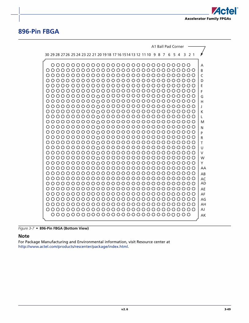
Axcelerator Family FPGAs
v2.6 3-49
896-Pin FBGA
NoteFor Package Manufacturing and Environmental information, visit Resource center athttp://www.actel.com/products/rescenter/package/index.html.
Figure 3-7 • 896-Pin FBGA (Bottom View)
A1 Ball Pad Corner
ABCDE
FGHJKLM
NPRTUVWYAA
ABACAD
AEAF
123456789101112131415161718192021222324252627282930
AGAHAJ
AK
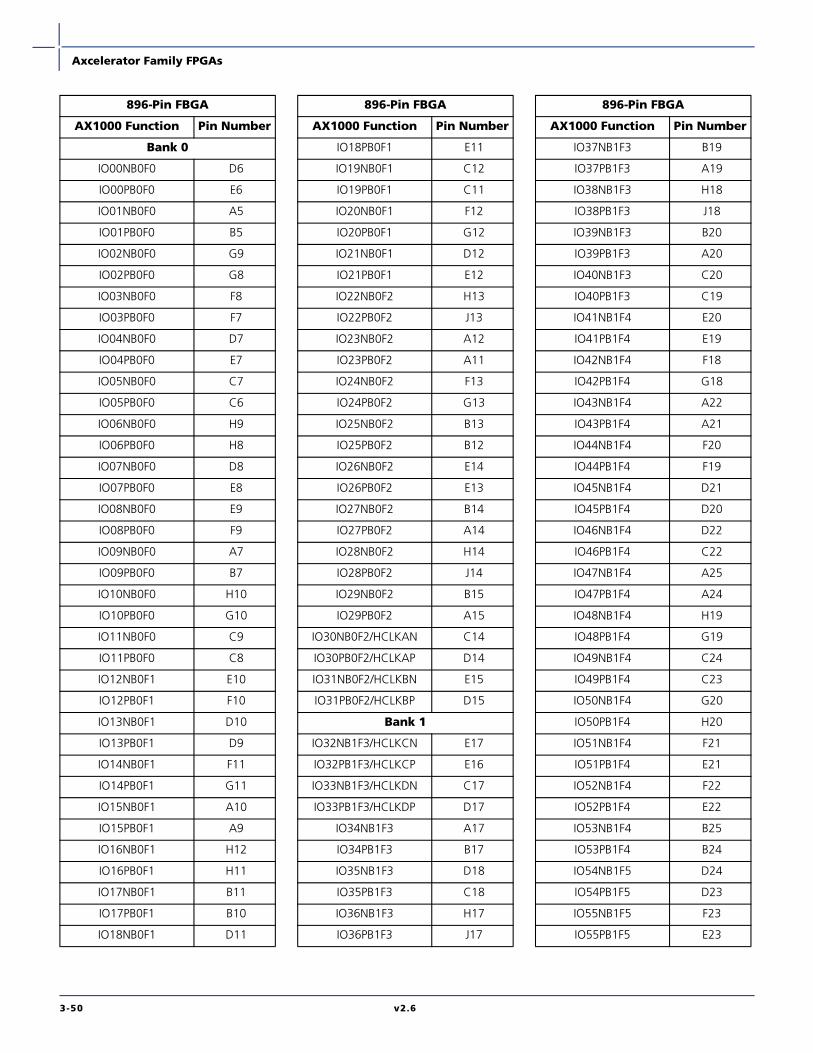
Axcelerator Family FPGAs
3-50 v2.6
896-Pin FBGA
AX1000 Function Pin Number
Bank 0
IO00NB0F0 D6
IO00PB0F0 E6
IO01NB0F0 A5
IO01PB0F0 B5
IO02NB0F0 G9
IO02PB0F0 G8
IO03NB0F0 F8
IO03PB0F0 F7
IO04NB0F0 D7
IO04PB0F0 E7
IO05NB0F0 C7
IO05PB0F0 C6
IO06NB0F0 H9
IO06PB0F0 H8
IO07NB0F0 D8
IO07PB0F0 E8
IO08NB0F0 E9
IO08PB0F0 F9
IO09NB0F0 A7
IO09PB0F0 B7
IO10NB0F0 H10
IO10PB0F0 G10
IO11NB0F0 C9
IO11PB0F0 C8
IO12NB0F1 E10
IO12PB0F1 F10
IO13NB0F1 D10
IO13PB0F1 D9
IO14NB0F1 F11
IO14PB0F1 G11
IO15NB0F1 A10
IO15PB0F1 A9
IO16NB0F1 H12
IO16PB0F1 H11
IO17NB0F1 B11
IO17PB0F1 B10
IO18NB0F1 D11
IO18PB0F1 E11
IO19NB0F1 C12
IO19PB0F1 C11
IO20NB0F1 F12
IO20PB0F1 G12
IO21NB0F1 D12
IO21PB0F1 E12
IO22NB0F2 H13
IO22PB0F2 J13
IO23NB0F2 A12
IO23PB0F2 A11
IO24NB0F2 F13
IO24PB0F2 G13
IO25NB0F2 B13
IO25PB0F2 B12
IO26NB0F2 E14
IO26PB0F2 E13
IO27NB0F2 B14
IO27PB0F2 A14
IO28NB0F2 H14
IO28PB0F2 J14
IO29NB0F2 B15
IO29PB0F2 A15
IO30NB0F2/HCLKAN C14
IO30PB0F2/HCLKAP D14
IO31NB0F2/HCLKBN E15
IO31PB0F2/HCLKBP D15
Bank 1
IO32NB1F3/HCLKCN E17
IO32PB1F3/HCLKCP E16
IO33NB1F3/HCLKDN C17
IO33PB1F3/HCLKDP D17
IO34NB1F3 A17
IO34PB1F3 B17
IO35NB1F3 D18
IO35PB1F3 C18
IO36NB1F3 H17
IO36PB1F3 J17
896-Pin FBGA
AX1000 Function Pin Number
IO37NB1F3 B19
IO37PB1F3 A19
IO38NB1F3 H18
IO38PB1F3 J18
IO39NB1F3 B20
IO39PB1F3 A20
IO40NB1F3 C20
IO40PB1F3 C19
IO41NB1F4 E20
IO41PB1F4 E19
IO42NB1F4 F18
IO42PB1F4 G18
IO43NB1F4 A22
IO43PB1F4 A21
IO44NB1F4 F20
IO44PB1F4 F19
IO45NB1F4 D21
IO45PB1F4 D20
IO46NB1F4 D22
IO46PB1F4 C22
IO47NB1F4 A25
IO47PB1F4 A24
IO48NB1F4 H19
IO48PB1F4 G19
IO49NB1F4 C24
IO49PB1F4 C23
IO50NB1F4 G20
IO50PB1F4 H20
IO51NB1F4 F21
IO51PB1F4 E21
IO52NB1F4 F22
IO52PB1F4 E22
IO53NB1F4 B25
IO53PB1F4 B24
IO54NB1F5 D24
IO54PB1F5 D23
IO55NB1F5 F23
IO55PB1F5 E23
896-Pin FBGA
AX1000 Function Pin Number

Axcelerator Family FPGAs
v2.6 3-51
IO56NB1F5 H21
IO56PB1F5 G21
IO57NB1F5 D25
IO57PB1F5 C25
IO58NB1F5 F24
IO58PB1F5 E24
IO59NB1F5 D26
IO59PB1F5 C26
IO60NB1F5 G23
IO60PB1F5 G22
IO61NB1F5 B27
IO61PB1F5 A27
IO62NB1F5 F25
IO62PB1F5 E25
IO63NB1F5 H23
IO63PB1F5 H22
Bank 2
IO64NB2F6 K23
IO64PB2F6 J23
IO65NB2F6 J24
IO65PB2F6 H24
IO66NB2F6 H26
IO66PB2F6 H25
IO67NB2F6 G26
IO67PB2F6 G25
IO68NB2F6 K25
IO68PB2F6 K24
IO69NB2F6 F27
IO69PB2F6 E27
IO70NB2F6 J26
IO70PB2F6 J25
IO71NB2F6 H27
IO71PB2F6 G27
IO72NB2F6 J28
IO72PB2F6 H28
IO73NB2F6 G28
IO73PB2F6 F28
IO74NB2F7 L23
896-Pin FBGA
AX1000 Function Pin Number
IO74PB2F7 L24
IO75NB2F7 L26
IO75PB2F7 K26
IO76NB2F7 M25
IO76PB2F7 L25
IO77NB2F7 K27
IO77PB2F7 J27
IO78NB2F7 M27
IO78PB2F7 L27
IO79NB2F7 K30
IO79PB2F7 K29
IO80NB2F7 M23
IO80PB2F7 M24
IO81NB2F7 M28
IO81PB2F7 L28
IO82NB2F7 N26
IO82PB2F7 M26
IO83NB2F7 N25
IO83PB2F7 N24
IO84NB2F7 N22
IO84PB2F7 N23
IO85NB2F8 M29
IO85PB2F8 L29
IO86NB2F8 N28
IO86PB2F8 N27
IO87NB2F8 P29
IO87PB2F8 P30
IO88NB2F8 P25
IO88PB2F8 P24
IO89NB2F8 P28
IO89PB2F8 P27
IO90NB2F8 P22
IO90PB2F8 P23
IO91NB2F8 R26
IO91PB2F8 P26
IO92NB2F8 R24
IO92PB2F8 R25
IO93NB2F8 R29
896-Pin FBGA
AX1000 Function Pin Number
IO93PB2F8 R30
IO94NB2F8 R22
IO94PB2F8 R23
IO95NB2F8 T27
IO95PB2F8 R27
Bank 3
IO96NB3F9 T29
IO96PB3F9 T30
IO97NB3F9 U29
IO97PB3F9 U30
IO98NB3F9 T22
IO98PB3F9 T23
IO99NB3F9 U26
IO99PB3F9 T26
IO100NB3F9 U24
IO100PB3F9 T24
IO101NB3F9 V28
IO101PB3F9 U28
IO102NB3F9 U23
IO102PB3F9 U22
IO103NB3F9 V27
IO103PB3F9 U27
IO104NB3F9 W29
IO104PB3F9 V29
IO105NB3F9 Y28
IO105PB3F9 W28
IO106NB3F9 V25
IO106PB3F9 U25
IO107NB3F10 W26
IO107PB3F10 V26
IO108NB3F10 W24
IO108PB3F10 V24
IO109NB3F10 Y27
IO109PB3F10 W27
IO110NB3F10 V23
IO110PB3F10 V22
IO111NB3F10 AA29
IO111PB3F10 Y29
896-Pin FBGA
AX1000 Function Pin Number

Axcelerator Family FPGAs
3-52 v2.6
IO112NB3F10 Y25
IO112PB3F10 W25
IO113NB3F10 AB27
IO113PB3F10 AA27
IO114NB3F10 Y23
IO114PB3F10 W23
IO115NB3F10 AA26
IO115PB3F10 Y26
IO116NB3F10 AC28
IO116PB3F10 AB28
IO117NB3F10 AE29
IO117PB3F10 AD29
IO118NB3F11 AE28
IO118PB3F11 AD28
IO119NB3F11 AD27
IO119PB3F11 AC27
IO120NB3F11 AA24
IO120PB3F11 Y24
IO121NB3F11 AB25
IO121PB3F11 AA25
IO122NB3F11 AC26
IO122PB3F11 AB26
IO123NB3F11 AG28
IO123PB3F11 AF28
IO124NB3F11 AB23
IO124PB3F11 AA23
IO125NB3F11 AF27
IO125PB3F11 AE27
IO126NB3F11 AD25
IO126PB3F11 AC25
IO127NB3F11 AE26
IO127PB3F11 AD26
IO128NB3F11 AC24
IO128PB3F11 AB24
Bank 4
IO129NB4F12 AD23
IO129PB4F12 AC23
IO130NB4F12 AK26
896-Pin FBGA
AX1000 Function Pin Number
IO130PB4F12 AK27
IO131NB4F12 AF24
IO131PB4F12 AF25
IO132NB4F12 AG25
IO132PB4F12 AG26
IO133NB4F12 AD22
IO133PB4F12 AC22
IO134NB4F12 AE23
IO134PB4F12 AE24
IO135NB4F12 AH24
IO135PB4F12 AH25
IO136NB4F12 AJ25
IO136PB4F12 AJ26
IO137NB4F12 AD21
IO137PB4F12 AC21
IO138NB4F12 AK24
IO138PB4F12 AK25
IO139NB4F13 AE21
IO139PB4F13 AE22
IO140NB4F13 AG23
IO140PB4F13 AG24
IO141NB4F13 AF22
IO141PB4F13 AF23
IO142NB4F13 AJ23
IO142PB4F13 AJ24
IO143NB4F13 AD19
IO143PB4F13 AD20
IO144NB4F13 AG21
IO144PB4F13 AG22
IO145NB4F13 AE19
IO145PB4F13 AE20
IO146NB4F13 AF20
IO146PB4F13 AF21
IO147NB4F13 AC19
IO147PB4F13 AC20
IO148NB4F13 AH22
IO148PB4F13 AH23
IO149NB4F13 AC18
896-Pin FBGA
AX1000 Function Pin Number
IO149PB4F13 AB18
IO150NB4F13 AK21
IO150PB4F13 AJ21
IO151NB4F13 AE18
IO151PB4F13 AD18
IO152NB4F14 AJ20
IO152PB4F14 AK20
IO153NB4F14 AG19
IO153PB4F14 AG20
IO154NB4F14 AH19
IO154PB4F14 AH20
IO155NB4F14 AC17
IO155PB4F14 AB17
IO156NB4F14 AK19
IO156PB4F14 AJ19
IO157NB4F14 AE17
IO157PB4F14 AD17
IO158NB4F14 AJ17
IO158PB4F14 AJ18
IO159NB4F14/CLKEN AG18
IO159PB4F14/CLKEP AH18
IO160NB4F14/CLKFN AG16
IO160PB4F14/CLKFP AG17
Bank 5
IO161NB5F15/CLKGN AG14
IO161PB5F15/CLKGP AG15
IO162NB5F15/CLKHN AG13
IO162PB5F15/CLKHP AH13
IO163NB5F15 AE14
IO163PB5F15 AD14
IO164NB5F15 AJ12
IO164PB5F15 AJ13
IO165NB5F15 AB14
IO165PB5F15 AC15
IO166NB5F15 AK11
IO166PB5F15 AK12
IO167NB5F15 AB13
IO167PB5F15 AC14
896-Pin FBGA
AX1000 Function Pin Number
Axcelerator Family FPGAs
v2.6 3-53
IO168NB5F15 AH11
IO168PB5F15 AH12
IO169NB5F15 AD13
IO169PB5F15 AC13
IO170NB5F15 AJ10
IO170PB5F15 AJ11
IO171NB5F16 AG11
IO171PB5F16 AG12
IO172NB5F16 AK9
IO172PB5F16 AK10
IO173NB5F16 AE12
IO173PB5F16 AE13
IO174NB5F16 AG9
IO174PB5F16 AG10
IO175NB5F16 AE11
IO175PB5F16 AF11
IO176NB5F16 AH8
IO176PB5F16 AH9
IO177NB5F16 AC12
IO177PB5F16 AD12
IO178NB5F16 AJ7
IO178PB5F16 AJ8
IO179NB5F16 AF9
IO179PB5F16 AF10
IO180NB5F16 AE9
IO180PB5F16 AE10
IO181NB5F17 AC11
IO181PB5F17 AD11
IO182NB5F17 AK6
IO182PB5F17 AK7
IO183NB5F17 AF8
IO183PB5F17 AG8
IO184NB5F17 AG7
IO184PB5F17 AH7
IO185NB5F17 AC10
IO185PB5F17 AD10
IO186NB5F17 AJ5
IO186PB5F17 AJ6
896-Pin FBGA
AX1000 Function Pin Number
IO187NB5F17 AE7
IO187PB5F17 AE8
IO188NB5F17 AF6
IO188PB5F17 AF7
IO189NB5F17 AD8
IO189PB5F17 AD9
IO190NB5F17 AH6
IO190PB5F17 AG6
IO191NB5F17 AG5
IO191PB5F17 AH5
IO192NB5F17 AC8
IO192PB5F17 AC9
Bank 6
IO193NB6F18 AB7
IO193PB6F18 AC7
IO194NB6F18 AD5
IO194PB6F18 AE5
IO195NB6F18 AB6
IO195PB6F18 AC6
IO196NB6F18 AE4
IO196PB6F18 AF4
IO197NB6F18 AA8
IO197PB6F18 AB8
IO198NB6F18 AF3
IO198PB6F18 AG3
IO199NB6F18 AC4
IO199PB6F18 AD4
IO200NB6F18 AB5
IO200PB6F18 AC5
IO201NB6F18 Y7
IO201PB6F18 AA7
IO202NB6F18 AD3
IO202PB6F18 AE3
IO203NB6F19 Y6
IO203PB6F19 AA6
IO204NB6F19 Y5
IO204PB6F19 AA5
IO205NB6F19 W8
896-Pin FBGA
AX1000 Function Pin Number
IO205PB6F19 Y8
IO206NB6F19 AA4
IO206PB6F19 AB4
IO207NB6F19 W6
IO207PB6F19 W7
IO208NB6F19 AB3
IO208PB6F19 AC3
IO209NB6F19 V8
IO209PB6F19 V9
IO210NB6F19 AA2
IO210PB6F19 AA1
IO211NB6F19 V5
IO211PB6F19 W5
IO212NB6F19 Y3
IO212PB6F19 Y4
IO213NB6F19 V7
IO213PB6F19 V6
IO214NB6F20 W3
IO214PB6F20 W4
IO215NB6F20 U8
IO215PB6F20 U9
IO216NB6F20 W1
IO216PB6F20 W2
IO217NB6F20 U7
IO217PB6F20 U6
IO218NB6F20 U4
IO218PB6F20 V4
IO219NB6F20 T5
IO219PB6F20 U5
IO220NB6F20 U3
IO220PB6F20 V3
IO221NB6F20 T8
IO221PB6F20 T9
IO222NB6F20 U2
IO222PB6F20 V2
IO223NB6F20 T7
IO223PB6F20 T6
IO224NB6F20 R2
896-Pin FBGA
AX1000 Function Pin Number

Axcelerator Family FPGAs
3-54 v2.6
IO224PB6F20 T2
Bank 7
IO225NB7F21 R7
IO225PB7F21 R6
IO226NB7F21 R4
IO226PB7F21 R5
IO227NB7F21 R8
IO227PB7F21 R9
IO228NB7F21 P1
IO228PB7F21 R1
IO229NB7F21 P9
IO229PB7F21 P8
IO230NB7F21 N2
IO230PB7F21 P2
IO231NB7F21 P7
IO231PB7F21 P6
IO232NB7F21 N3
IO232PB7F21 P3
IO233NB7F21 P4
IO233PB7F21 P5
IO234NB7F21 L1
IO234PB7F21 M1
IO235NB7F21 M4
IO235PB7F21 N4
IO236NB7F22 N7
IO236PB7F22 N6
IO237NB7F22 N8
IO237PB7F22 N9
IO238NB7F22 M5
IO238PB7F22 N5
IO239NB7F22 L2
IO239PB7F22 M2
IO240NB7F22 L3
IO240PB7F22 M3
IO241NB7F22 M8
IO241PB7F22 M7
IO242NB7F22 K4
IO242PB7F22 L4
896-Pin FBGA
AX1000 Function Pin Number
IO243NB7F22 L6
IO243PB7F22 M6
IO244NB7F22 K5
IO244PB7F22 L5
IO245NB7F22 J4
IO245PB7F22 J3
IO246NB7F22 G2
IO246PB7F22 H2
IO247NB7F23 L8
IO247PB7F23 L7
IO248NB7F23 G3
IO248PB7F23 H3
IO249NB7F23 G4
IO249PB7F23 H4
IO250NB7F23 J6
IO250PB7F23 K6
IO251NB7F23 H5
IO251PB7F23 J5
IO252NB7F23 F2
IO252PB7F23 F1
IO253NB7F23 K8
IO253PB7F23 K7
IO254NB7F23 F4
IO254PB7F23 F3
IO255NB7F23 G6
IO255PB7F23 H6
IO256NB7F23 F5
IO256PB7F23 G5
IO257NB7F23 H7
IO257PB7F23 J7
Dedicated I/O
GND A13
GND A18
GND A2
GND A23
GND A29
GND A8
GND AA10
896-Pin FBGA
AX1000 Function Pin Number
GND AA21
GND AA28
GND AA3
GND AB2
GND AB22
GND AB29
GND AB9
GND AC1
GND AC30
GND AE25
GND AE6
GND AF26
GND AF5
GND AG27
GND AG4
GND AH10
GND AH15
GND AH16
GND AH21
GND AH28
GND AH3
GND AJ1
GND AJ2
GND AJ22
GND AJ29
GND AJ30
GND AJ9
GND AK13
GND AK18
GND AK2
GND AK23
GND AK29
GND AK8
GND B1
GND B2
GND B22
GND B29
GND B30
896-Pin FBGA
AX1000 Function Pin Number

Axcelerator Family FPGAs
v2.6 3-55
GND B9
GND C10
GND C15
GND C16
GND C21
GND C28
GND C3
GND D27
GND D28
GND D4
GND E26
GND E5
GND H1
GND H30
GND J2
GND J22
GND J29
GND J9
GND K10
GND K21
GND K28
GND K3
GND L11
GND L20
GND M12
GND M13
GND M14
GND M15
GND M16
GND M17
GND M18
GND M19
GND N1
GND N12
GND N13
GND N14
GND N15
GND N16
896-Pin FBGA
AX1000 Function Pin Number
GND N17
GND N18
GND N19
GND N30
GND P12
GND P13
GND P14
GND P15
GND P16
GND P17
GND P18
GND P19
GND R12
GND R13
GND R14
GND R15
GND R16
GND R17
GND R18
GND R19
GND R28
GND R3
GND T12
GND T13
GND T14
GND T15
GND T16
GND T17
GND T18
GND T19
GND T28
GND T3
GND U12
GND U13
GND U14
GND U15
GND U16
GND U17
896-Pin FBGA
AX1000 Function Pin Number
GND U18
GND U19
GND V1
GND V12
GND V13
GND V14
GND V15
GND V16
GND V17
GND V18
GND V19
GND V30
GND W12
GND W13
GND W14
GND W15
GND W16
GND W17
GND W18
GND W19
GND Y11
GND Y20
GND/LP E4
NC A16
NC A26
NC A4
NC A6
NC AA30
NC AB1
NC AB30
NC AC2
NC AC29
NC AD1
NC AD2
NC AD30
NC AE1
NC AE15
NC AE16
896-Pin FBGA
AX1000 Function Pin Number
Axcelerator Family FPGAs
3-56 v2.6
NC AE2
NC AE30
NC AF1
NC AF2
NC AF29
NC AF30
NC AG1
NC AG2
NC AG29
NC AG30
NC AH27
NC AH4
NC AJ14
NC AJ15
NC AJ16
NC AJ27
NC AJ4
NC AK14
NC AK15
NC AK16
NC AK17
NC AK22
NC AK4
NC AK5
NC B16
NC B18
NC B21
NC B23
NC B26
NC B4
NC B6
NC B8
NC C27
NC D1
NC D2
NC D29
NC D30
NC E1
896-Pin FBGA
AX1000 Function Pin Number
NC E2
NC E29
NC E30
NC F15
NC F16
NC F29
NC F30
NC G1
NC G29
NC G30
NC H29
NC J1
NC J30
NC K1
NC K2
NC L30
NC M30
NC N29
NC T1
NC U1
NC W30
NC Y1
NC Y2
NC Y30
PRA G15
PRB D16
PRC AB16
PRD AF16
TCK G7
TDI D5
TDO J8
TMS F6
TRST C4
VCCA AD6
VCCA AH26
VCCA E28
VCCA E3
VCCA L12
896-Pin FBGA
AX1000 Function Pin Number
VCCA L13
VCCA L14
VCCA L15
VCCA L16
VCCA L17
VCCA L18
VCCA L19
VCCA M11
VCCA M20
VCCA N11
VCCA N20
VCCA P11
VCCA P20
VCCA R11
VCCA R20
VCCA T11
VCCA T20
VCCA U11
VCCA U20
VCCA V11
VCCA V20
VCCA W11
VCCA W20
VCCA Y12
VCCA Y13
VCCA Y14
VCCA Y15
VCCA Y16
VCCA Y17
VCCA Y18
VCCA Y19
VCCPLA G14
VCCPLB H15
VCCPLC G17
VCCPLD J16
VCCPLE AH17
VCCPLF AC16
VCCPLG AH14
896-Pin FBGA
AX1000 Function Pin Number
Axcelerator Family FPGAs
v2.6 3-57
VCCPLH AD15
VCCDA AD24
VCCDA AD7
VCCDA AF12
VCCDA AF13
VCCDA AF15
VCCDA AF18
VCCDA AF19
VCCDA C13
VCCDA C5
VCCDA D13
VCCDA D19
VCCDA D3
VCCDA E18
VCCDA F26
VCCDA G16
VCCDA T25
VCCDA T4
VCCIB0 A3
VCCIB0 B3
VCCIB0 J10
VCCIB0 J11
VCCIB0 J12
VCCIB0 K11
VCCIB0 K12
VCCIB0 K13
VCCIB0 K14
VCCIB0 K15
VCCIB1 A28
VCCIB1 B28
VCCIB1 J19
VCCIB1 J20
VCCIB1 J21
VCCIB1 K16
VCCIB1 K17
VCCIB1 K18
VCCIB1 K19
VCCIB1 K20
896-Pin FBGA
AX1000 Function Pin Number
VCCIB2 C29
VCCIB2 C30
VCCIB2 K22
VCCIB2 L21
VCCIB2 L22
VCCIB2 M21
VCCIB2 M22
VCCIB2 N21
VCCIB2 P21
VCCIB2 R21
VCCIB3 AA22
VCCIB3 AH29
VCCIB3 AH30
VCCIB3 T21
VCCIB3 U21
VCCIB3 V21
VCCIB3 W21
VCCIB3 W22
VCCIB3 Y21
VCCIB3 Y22
VCCIB4 AA16
VCCIB4 AA17
VCCIB4 AA18
VCCIB4 AA19
VCCIB4 AA20
VCCIB4 AB19
VCCIB4 AB20
VCCIB4 AB21
VCCIB4 AJ28
VCCIB4 AK28
VCCIB5 AA11
VCCIB5 AA12
VCCIB5 AA13
VCCIB5 AA14
VCCIB5 AA15
VCCIB5 AB10
VCCIB5 AB11
VCCIB5 AB12
896-Pin FBGA
AX1000 Function Pin Number
VCCIB5 AJ3
VCCIB5 AK3
VCCIB6 AA9
VCCIB6 AH1
VCCIB6 AH2
VCCIB6 T10
VCCIB6 U10
VCCIB6 V10
VCCIB6 W10
VCCIB6 W9
VCCIB6 Y10
VCCIB6 Y9
VCCIB7 C1
VCCIB7 C2
VCCIB7 K9
VCCIB7 L10
VCCIB7 L9
VCCIB7 M10
VCCIB7 M9
VCCIB7 N10
VCCIB7 P10
VCCIB7 R10
VCOMPLA F14
VCOMPLB J15
VCOMPLC F17
VCOMPLD H16
VCOMPLE AF17
VCOMPLF AD16
VCOMPLG AF14
VCOMPLH AB15
VPUMP G24
896-Pin FBGA
AX1000 Function Pin Number

Axcelerator Family FPGAs
3-58 v2.6
896-Pin FBGA
AX2000 Function Pin Number
Bank 0
IO00NB0F0 B4
IO00PB0F0 A4
IO01NB0F0 F8
IO01PB0F0 F7
IO02NB0F0 D6
IO02PB0F0 E6
IO04NB0F0 A5
IO04PB0F0 B5
IO05NB0F0 H8
IO05PB0F0 G8
IO06NB0F0 D7
IO06PB0F0 E7
IO07NB0F0 D8
IO07PB0F0 E8
IO08NB0F0 C7
IO08PB0F0 C6
IO09NB0F0 G9
IO09PB0F0 H9
IO10NB0F0 A6
IO10PB0F0 B6
IO11NB0F0 H10
IO11PB0F0 G10
IO12NB0F1 E9
IO12PB0F1 F9
IO13NB0F1 E10
IO13PB0F1 F10
IO15NB0F1 F11
IO15PB0F1 G11
IO16NB0F1 A7
IO16PB0F1 B7
IO17NB0F1 D10
IO17PB0F1 D9
IO18NB0F1 C9
* Not routed on the same package layerand to adjacent LGA pads as its differentialpair complement. Recommended to beused as a single-ended I/O.
IO18PB0F1 C8
IO19NB0F1 D11
IO19PB0F1 E11
IO20PB0F1 B8
IO21NB0F1 H12
IO21PB0F1 H11
IO23NB0F2 A10
IO23PB0F2 A9
IO25NB0F2 F12
IO25PB0F2 G12
IO26NB0F2 B11
IO26PB0F2 B10
IO27NB0F2 D12
IO27PB0F2 E12
IO28NB0F2 C12
IO28PB0F2 C11
IO30NB0F2 A12
IO30PB0F2 A11
IO31NB0F2 F13
IO31PB0F2 G13
IO33NB0F2 H13
IO33PB0F2 J13
IO34NB0F3 B13
IO34PB0F3 B12
IO37NB0F3 E14
IO37PB0F3 E13
IO38NB0F3 B14
IO38PB0F3 A14
IO39NB0F3 H14
IO39PB0F3 J14
IO40NB0F3 B15
IO40PB0F3 A15
IO41NB0F3/HCLKAN C14
IO41PB0F3/HCLKAP D14
896-Pin FBGA
AX2000 Function Pin Number
* Not routed on the same package layerand to adjacent LGA pads as its differentialpair complement. Recommended to beused as a single-ended I/O.
IO42NB0F3/HCLKBN E15
IO42PB0F3/HCLKBP D15
Bank 1
IO43NB1F4/HCLKCN E17
IO43PB1F4/HCLKCP E16
IO44NB1F4/HCLKDN C17
IO44PB1F4/HCLKDP D17
IO45NB1F4 A16
IO45PB1F4 B16
IO47NB1F4 H17
IO47PB1F4 J17
IO48NB1F4 A17
IO48PB1F4 B17
IO49NB1F4 H18
IO49PB1F4 J18
IO51NB1F4 F18
IO51PB1F4 G18
IO52NB1F4 B18
IO53NB1F4 D18
IO53PB1F4 C18
IO55NB1F5 H19
IO55PB1F5 G19
IO56NB1F5 B19
IO56PB1F5 A19
IO57NB1F5 E20
IO57PB1F5 E19
IO58NB1F5 C20
IO58PB1F5 C19
IO59NB1F5 B20
IO59PB1F5 A20
IO61NB1F5 F20
IO61PB1F5 F19
IO62NB1F5 A22
IO62PB1F5 A21
896-Pin FBGA
AX2000 Function Pin Number
* Not routed on the same package layerand to adjacent LGA pads as its differentialpair complement. Recommended to beused as a single-ended I/O.

Axcelerator Family FPGAs
v2.6 3-59
IO63NB1F5 D21
IO63PB1F5 D20
IO65NB1F6 G20
IO65PB1F6 H20
IO66NB1F6 B23
IO66PB1F6 B21
IO67NB1F6 H21
IO67PB1F6 G21
IO68NB1F6 D22
IO68PB1F6 C22
IO69NB1F6 A25
IO69PB1F6 A24
IO70NB1F6 F22
IO70PB1F6 E22
IO71NB1F6 F21
IO71PB1F6 E21
IO73NB1F6 C24
IO73PB1F6 C23
IO74NB1F6 D24
IO74PB1F6 D23
IO75NB1F6 H23
IO75PB1F6 H22
IO76NB1F7 B25
IO76PB1F7 B24
IO78NB1F7 B26
IO78PB1F7 A26
IO79NB1F7 F23
IO79PB1F7 E23
IO80NB1F7 D25
IO80PB1F7 C25
IO81NB1F7 G23
IO81PB1F7 G22
IO82NB1F7 B27
IO82PB1F7 A27
896-Pin FBGA
AX2000 Function Pin Number
* Not routed on the same package layerand to adjacent LGA pads as its differentialpair complement. Recommended to beused as a single-ended I/O.
IO83NB1F7 F24
IO83PB1F7 E24
IO84NB1F7 D26
IO84PB1F7 C26
IO85NB1F7 F25
IO85PB1F7 E25
Bank 2
IO86NB2F8 G26
IO86PB2F8 G25
IO87NB2F8 K23
IO87PB2F8 J23
IO88NB2F8 J24
IO88PB2F8 H24
IO89NB2F8 E29
IO89PB2F8 D29
IO90NB2F8 F27
IO90PB2F8 E27
IO91NB2F8 H26
IO91PB2F8 H25
IO92NB2F8 G28
IO92PB2F8 F28
IO93NB2F8 J26
IO93PB2F8 J25
IO94NB2F8 H27
IO94PB2F8 G27
IO95NB2F8 H29
IO95PB2F8 G29
IO96NB2F9 G30
IO96PB2F9 F30
IO97NB2F9 K25
IO97PB2F9 K24
IO98NB2F9 J28
IO98PB2F9 H28
IO99NB2F9 L23
896-Pin FBGA
AX2000 Function Pin Number
* Not routed on the same package layerand to adjacent LGA pads as its differentialpair complement. Recommended to beused as a single-ended I/O.
IO99PB2F9 L24
IO100NB2F9 K27
IO100PB2F9 J27
IO101PB2F9 J30
IO102NB2F9 E30
IO102PB2F9 D30
IO103NB2F9 L26
IO103PB2F9 K26
IO104NB2F9 F29
IO105NB2F9 M25
IO105PB2F9 L25
IO106NB2F9 K30
IO106PB2F9 K29
IO107NB2F10 M23
IO107PB2F10 M24
IO109NB2F10 M27
IO109PB2F10 L27
IO110NB2F10 M28
IO110PB2F10 L28
IO111NB2F10 N22
IO111PB2F10 N23
IO112NB2F10 M29
IO112PB2F10 L29
IO113NB2F10 N26
IO113PB2F10 M26
IO114NB2F10 M30
IO114PB2F10 L30
IO115NB2F10 N28
IO115PB2F10 N27
IO117NB2F10 N25
IO117PB2F10 N24
IO118NB2F11 N29
IO119NB2F11 P22
IO119PB2F11 P23
896-Pin FBGA
AX2000 Function Pin Number
* Not routed on the same package layerand to adjacent LGA pads as its differentialpair complement. Recommended to beused as a single-ended I/O.

Axcelerator Family FPGAs
3-60 v2.6
IO121NB2F11 P25
IO121PB2F11 P24
IO122NB2F11 P28
IO122PB2F11 P27
IO123NB2F11 R26
IO123PB2F11 P26
IO124NB2F11 P29
IO124PB2F11 P30
IO125NB2F11 R22
IO125PB2F11 R23
IO127NB2F11 R24
IO127PB2F11 R25
IO128NB2F11 R29
IO128PB2F11 R30
Bank 3
IO129NB3F12 T27
IO129PB3F12 R27
IO130NB3F12 T29
IO130PB3F12 T30
IO131NB3F12 T22
IO131PB3F12 T23
IO132NB3F12 U26
IO132PB3F12 T26
IO133NB3F12 U24
IO133PB3F12 T24
IO135NB3F12 U23
IO135PB3F12 U22
IO136NB3F12 U29
IO136PB3F12 U30
IO137NB3F12 V28
IO137PB3F12 U28
IO138NB3F12 V27
IO138PB3F12 U27
IO139NB3F13 V25
896-Pin FBGA
AX2000 Function Pin Number
* Not routed on the same package layerand to adjacent LGA pads as its differentialpair complement. Recommended to beused as a single-ended I/O.
IO139PB3F13 U25
IO141NB3F13 V23
IO141PB3F13 V22
IO142NB3F13 W29
IO142PB3F13 V29
IO143NB3F13 W26
IO143PB3F13 V26
IO145NB3F13 W24
IO145PB3F13 V24
IO146NB3F13 W27
IO146PB3F13 W28
IO147NB3F13 Y28
IO147PB3F13 Y27
IO148NB3F13 Y30
IO148PB3F13 W30
IO149NB3F13 Y25
IO149PB3F13 W25
IO150NB3F14 AA29
IO150PB3F14 Y29
IO151NB3F14 AC29
IO152NB3F14 AA26
IO152PB3F14 Y26
IO153NB3F14 Y23
IO153PB3F14 W23
IO154NB3F14 AB30
IO154PB3F14 AA30
IO155NB3F14 AB27
IO155PB3F14 AA27
IO156NB3F14 AC28
IO156PB3F14 AB28
IO157NB3F14 AA24
IO157PB3F14 Y24
IO158NB3F14 AF29
IO158PB3F14 AF30
896-Pin FBGA
AX2000 Function Pin Number
* Not routed on the same package layerand to adjacent LGA pads as its differentialpair complement. Recommended to beused as a single-ended I/O.
IO159NB3F14 AB25
IO159PB3F14 AA25
IO160NB3F14 AE30
IO160PB3F14 AD30
IO161NB3F15 AE29
IO161PB3F15 AD29
IO162NB3F15 AD27
IO162PB3F15 AC27
IO163NB3F15 AC26
IO163PB3F15 AB26
IO164NB3F15 AE28
IO164PB3F15 AD28
IO165NB3F15 AC24
IO165PB3F15 AB24
IO166NB3F15 AG28
IO166PB3F15 AF28
IO167NB3F15 AE26
IO167PB3F15 AD26
IO168NB3F15 AD25
IO168PB3F15 AC25
IO169NB3F15 AF27
IO169PB3F15 AE27
IO170NB3F15 AB23
IO170PB3F15 AA23
Bank 4
IO171NB4F16 AG29
IO171PB4F16 AG30
IO172NB4F16 AF24
IO172PB4F16 AF25
IO173NB4F16 AG25
IO173PB4F16 AG26
IO174NB4F16 AJ25
IO174PB4F16 AJ26
IO175NB4F16 AK26
896-Pin FBGA
AX2000 Function Pin Number
* Not routed on the same package layerand to adjacent LGA pads as its differentialpair complement. Recommended to beused as a single-ended I/O.

Axcelerator Family FPGAs
v2.6 3-61
IO175PB4F16 AK27
IO176NB4F16 AE23
IO176PB4F16 AE24
IO177NB4F16 AH24
IO177PB4F16 AH25
IO178NB4F16 AD23
IO178PB4F16 AC23
IO179PB4F16 AJ27
IO180NB4F16 AG23
IO180PB4F16 AG24
IO181NB4F17 AK24
IO181PB4F17 AK25
IO182NB4F17 AD22
IO182PB4F17 AC22
IO183NB4F17 AF22
IO183PB4F17 AF23
IO184NB4F17 AE21
IO184PB4F17 AE22
IO185NB4F17 AJ23
IO185PB4F17 AJ24
IO187NB4F17 AH22
IO187PB4F17 AH23
IO188NB4F17 AD21
IO188PB4F17 AC21
IO189PB4F17 AK22
IO190NB4F17 AF20
IO190PB4F17 AF21
IO191NB4F17 AG21
IO191PB4F17 AG22
IO192NB4F17 AE19
IO192PB4F17 AE20
IO195NB4F18 AK21
IO195PB4F18 AJ21
IO196NB4F18 AD19
896-Pin FBGA
AX2000 Function Pin Number
* Not routed on the same package layerand to adjacent LGA pads as its differentialpair complement. Recommended to beused as a single-ended I/O.
IO196PB4F18 AD20
IO197NB4F18 AJ20
IO197PB4F18 AK20
IO198NB4F18 AC19
IO198PB4F18 AC20
IO199NB4F18 AG19
IO199PB4F18 AG20
IO200NB4F18 AH19
IO200PB4F18 AH20
IO201NB4F18 AK19
IO201PB4F18 AJ19
IO202NB4F18 AC18
IO202PB4F18 AB18
IO206NB4F19 AE18
IO206PB4F19 AD18
IO207NB4F19 AJ17
IO207PB4F19 AJ18
IO208NB4F19 AE17
IO208PB4F19 AD17
IO209NB4F19 AK17
IO210NB4F19 AC17
IO210PB4F19 AB17
IO211NB4F19 AJ16
IO211PB4F19 AK16
IO212NB4F19/CLKEN AG18
IO212PB4F19/CLKEP AH18
IO213NB4F19/CLKFN AG16
IO213PB4F19/CLKFP AG17
Bank 5
IO214NB5F20/CLKGN AG14
IO214PB5F20/CLKGP AG15
IO215NB5F20/CLKHN AG13
IO215PB5F20/CLKHP AH13
IO216NB5F20 AB14
896-Pin FBGA
AX2000 Function Pin Number
* Not routed on the same package layerand to adjacent LGA pads as its differentialpair complement. Recommended to beused as a single-ended I/O.
IO216PB5F20 AC15
IO217NB5F20 AK15
IO217PB5F20 AJ15
IO218NB5F20 AE14
IO218PB5F20 AD14
IO219NB5F20 AK14
IO219PB5F20 AJ14
IO222NB5F20 AB13
IO222PB5F20 AC14
IO223NB5F21 AJ12
IO223PB5F21 AJ13
IO225NB5F21 AH11
IO225PB5F21 AH12
IO226NB5F21 AC13
IO226PB5F21 AD13
IO227NB5F21 AE12
IO227PB5F21 AE13
IO228NB5F21 AG11
IO228PB5F21 AG12
IO229NB5F21 AK11
IO229PB5F21 AK12
IO230NB5F21 AC12
IO230PB5F21 AD12
IO232NB5F21 AE11
IO232PB5F21 AF11
IO233NB5F21 AJ10
IO233PB5F21 AJ11
IO234NB5F21 AC11
IO234PB5F21 AD11
IO236NB5F22 AK9
IO236PB5F22 AK10
IO237NB5F22 AG9
IO237PB5F22 AG10
IO238NB5F22 AF9
896-Pin FBGA
AX2000 Function Pin Number
* Not routed on the same package layerand to adjacent LGA pads as its differentialpair complement. Recommended to beused as a single-ended I/O.

Axcelerator Family FPGAs
3-62 v2.6
IO238PB5F22 AF10
IO239NB5F22 AH8
IO239PB5F22 AH9
IO240NB5F22 AC10
IO240PB5F22 AD10
IO242NB5F22 AE9
IO242PB5F22 AE10
IO243NB5F22 AJ7
IO243PB5F22 AJ8
IO244NB5F22 AK6
IO244PB5F22 AK7
IO245NB5F23 AF8
IO245PB5F23 AG8
IO246NB5F23 AD8
IO246PB5F23 AD9
IO247NB5F23 AG7
IO247PB5F23 AH7
IO248NB5F23 AK5
IO249NB5F23 AJ5
IO249PB5F23 AJ6
IO250NB5F23 AC8
IO250PB5F23 AC9
IO251NB5F23 AH6
IO251PB5F23 AG6
IO252NB5F23 AF6
IO252PB5F23 AF7
IO253NB5F23 AG2
IO253PB5F23 AG1
IO254NB5F23 AE7
IO254PB5F23 AE8
IO255NB5F23 AG5
IO255PB5F23 AH5
IO256NB5F23 AJ4
IO256PB5F23 AK4
896-Pin FBGA
AX2000 Function Pin Number
* Not routed on the same package layerand to adjacent LGA pads as its differentialpair complement. Recommended to beused as a single-ended I/O.
Bank 6
IO257NB6F24 AE4
IO257PB6F24 AF4
IO258NB6F24 AB7
IO258PB6F24 AC7
IO259NB6F24 AD5
IO259PB6F24 AE5
IO260NB6F24 AF1
IO260PB6F24 AF2
IO261NB6F24 AF3
IO261PB6F24 AG3
IO262NB6F24 AC4
IO262PB6F24 AD4
IO263NB6F24 AD3
IO263PB6F24 AE3
IO264NB6F24 AB6
IO264PB6F24 AC6
IO265NB6F24 AD1
IO265PB6F24 AE1
IO266NB6F24 AA8
IO266PB6F24 AB8
IO267NB6F25 AB5
IO267PB6F25 AC5
IO268NB6F25 AB3
IO268PB6F25 AC3
IO269NB6F25 AC2
IO269PB6F25 AD2
IO270NB6F25 Y7
IO270PB6F25 AA7
IO271NB6F25 AA4
IO271PB6F25 AB4
IO272NB6F25 Y6
IO272PB6F25 AA6
IO273NB6F25 AB1*
896-Pin FBGA
AX2000 Function Pin Number
* Not routed on the same package layerand to adjacent LGA pads as its differentialpair complement. Recommended to beused as a single-ended I/O.
IO273PB6F25 AE2*
IO274NB6F25 W8
IO274PB6F25 Y8
IO275NB6F25 Y5
IO275PB6F25 AA5
IO277NB6F25 AA2
IO277PB6F25 AA1
IO278NB6F26 W6
IO278PB6F26 W7
IO279NB6F26 Y3
IO279PB6F26 Y4
IO280NB6F26 V8
IO280PB6F26 V9
IO281NB6F26 Y1
IO281PB6F26 Y2
IO282NB6F26 V5
IO282PB6F26 W5
IO284NB6F26 V7
IO284PB6F26 V6
IO285NB6F26 W3
IO285PB6F26 W4
IO286NB6F26 U8
IO286PB6F26 U9
IO287NB6F26 W1
IO287PB6F26 W2
IO288NB6F26 U7
IO288PB6F26 U6
IO290NB6F27 U4
IO290PB6F27 V4
IO291NB6F27 U3
IO291PB6F27 V3
IO292NB6F27 T5
IO292PB6F27 U5
IO293NB6F27 U2
896-Pin FBGA
AX2000 Function Pin Number
* Not routed on the same package layerand to adjacent LGA pads as its differentialpair complement. Recommended to beused as a single-ended I/O.

Axcelerator Family FPGAs
v2.6 3-63
IO293PB6F27 V2
IO294NB6F27 T8
IO294PB6F27 T9
IO296NB6F27 T1
IO296PB6F27 U1
IO298NB6F27 T7
IO298PB6F27 T6
IO299NB6F27 R2
IO299PB6F27 T2
Bank 7
IO300NB7F28 R8
IO300PB7F28 R9
IO302NB7F28 R4
IO302PB7F28 R5
IO303NB7F28 P1
IO303PB7F28 R1
IO304NB7F28 R7
IO304PB7F28 R6
IO306NB7F28 N2
IO306PB7F28 P2
IO307NB7F28 N3
IO307PB7F28 P3
IO308NB7F28 P9
IO308PB7F28 P8
IO309NB7F28 P4
IO309PB7F28 P5
IO310NB7F29 P7
IO310PB7F29 P6
IO311NB7F29 L1
IO311PB7F29 M1
IO312NB7F29 M5
IO312PB7F29 N5
IO313NB7F29 M4
IO313PB7F29 N4
896-Pin FBGA
AX2000 Function Pin Number
* Not routed on the same package layerand to adjacent LGA pads as its differentialpair complement. Recommended to beused as a single-ended I/O.
IO315NB7F29 L2
IO315PB7F29 M2
IO316NB7F29 N7
IO316PB7F29 N6
IO317NB7F29 L3
IO317PB7F29 M3
IO318NB7F29 N8
IO318PB7F29 N9
IO320NB7F29 L6
IO320PB7F29 M6
IO321NB7F30 K4
IO321PB7F30 L4
IO322NB7F30 M8
IO322PB7F30 M7
IO323NB7F30 J1
IO323PB7F30 K1
IO324NB7F30 K5
IO324PB7F30 L5
IO326NB7F30 G1*
IO326PB7F30 K2*
IO327NB7F30 J4
IO327PB7F30 J3
IO328NB7F30 L8
IO328PB7F30 L7
IO329NB7F30 G2
IO329PB7F30 H2
IO330NB7F30 G3
IO330PB7F30 H3
IO331NB7F30 K8
IO331PB7F30 K7
IO332NB7F31 J6
IO332PB7F31 K6
IO333NB7F31 D1
IO333PB7F31 D2
896-Pin FBGA
AX2000 Function Pin Number
* Not routed on the same package layerand to adjacent LGA pads as its differentialpair complement. Recommended to beused as a single-ended I/O.
IO334NB7F31 G4
IO334PB7F31 H4
IO335NB7F31 F2
IO335PB7F31 F1
IO336NB7F31 H5
IO336PB7F31 J5
IO337NB7F31 E2
IO337PB7F31 E1
IO338NB7F31 H7
IO338PB7F31 J7
IO339NB7F31 F4
IO339PB7F31 F3
IO340NB7F31 F5
IO340PB7F31 G5
IO341NB7F31 G6
IO341PB7F31 H6
Dedicated I/O
GND A13
GND A18
GND A2
GND A23
GND A29
GND A8
GND AA10
GND AA21
GND AA28
GND AA3
GND AB2
GND AB22
GND AB29
GND AB9
GND AC1
GND AC30
GND AE25
896-Pin FBGA
AX2000 Function Pin Number
* Not routed on the same package layerand to adjacent LGA pads as its differentialpair complement. Recommended to beused as a single-ended I/O.
Axcelerator Family FPGAs
3-64 v2.6
GND AE6
GND AF26
GND AF5
GND AG27
GND AG4
GND AH10
GND AH15
GND AH16
GND AH21
GND AH28
GND AH3
GND AJ1
GND AJ2
GND AJ22
GND AJ29
GND AJ30
GND AJ9
GND AK13
GND AK18
GND AK2
GND AK23
GND AK29
GND AK8
GND B1
GND B2
GND B22
GND B29
GND B30
GND B9
GND C10
GND C15
GND C16
GND C21
GND C28
896-Pin FBGA
AX2000 Function Pin Number
* Not routed on the same package layerand to adjacent LGA pads as its differentialpair complement. Recommended to beused as a single-ended I/O.
GND C3
GND D27
GND D28
GND D4
GND E26
GND E5
GND H1
GND H30
GND J2
GND J22
GND J29
GND J9
GND K10
GND K21
GND K28
GND K3
GND L11
GND L20
GND M12
GND M13
GND M14
GND M15
GND M16
GND M17
GND M18
GND M19
GND N1
GND N12
GND N13
GND N14
GND N15
GND N16
GND N17
GND N18
896-Pin FBGA
AX2000 Function Pin Number
* Not routed on the same package layerand to adjacent LGA pads as its differentialpair complement. Recommended to beused as a single-ended I/O.
GND N19
GND N30
GND P12
GND P13
GND P14
GND P15
GND P16
GND P17
GND P18
GND P19
GND R12
GND R13
GND R14
GND R15
GND R16
GND R17
GND R18
GND R19
GND R28
GND R3
GND T12
GND T13
GND T14
GND T15
GND T16
GND T17
GND T18
GND T19
GND T28
GND T3
GND U12
GND U13
GND U14
GND U15
896-Pin FBGA
AX2000 Function Pin Number
* Not routed on the same package layerand to adjacent LGA pads as its differentialpair complement. Recommended to beused as a single-ended I/O.

Axcelerator Family FPGAs
v2.6 3-65
GND U16
GND U17
GND U18
GND U19
GND V1
GND V12
GND V13
GND V14
GND V15
GND V16
GND V17
GND V18
GND V19
GND V30
GND W12
GND W13
GND W14
GND W15
GND W16
GND W17
GND W18
GND W19
GND Y11
GND Y20
GND/LP E4
PRA G15
PRB D16
PRC AB16
PRD AF16
TCK G7
TDI D5
TDO J8
TMS F6
TRST C4
896-Pin FBGA
AX2000 Function Pin Number
* Not routed on the same package layerand to adjacent LGA pads as its differentialpair complement. Recommended to beused as a single-ended I/O.
VCCA AD6
VCCA AH26
VCCA E28
VCCA E3
VCCA L12
VCCA L13
VCCA L14
VCCA L15
VCCA L16
VCCA L17
VCCA L18
VCCA L19
VCCA M11
VCCA M20
VCCA N11
VCCA N20
VCCA P11
VCCA P20
VCCA R11
VCCA R20
VCCA T11
VCCA T20
VCCA U11
VCCA U20
VCCA V11
VCCA V20
VCCA W11
VCCA W20
VCCA Y12
VCCA Y13
VCCA Y14
VCCA Y15
VCCA Y16
VCCA Y17
896-Pin FBGA
AX2000 Function Pin Number
* Not routed on the same package layerand to adjacent LGA pads as its differentialpair complement. Recommended to beused as a single-ended I/O.
VCCA Y18
VCCA Y19
VCCDA AD24
VCCDA AD7
VCCDA AE15
VCCDA AE16
VCCDA AF12
VCCDA AF13
VCCDA AF15
VCCDA AF18
VCCDA AF19
VCCDA AH27
VCCDA AH4
VCCDA C13
VCCDA C27
VCCDA C5
VCCDA D13
VCCDA D19
VCCDA D3
VCCDA E18
VCCDA F15
VCCDA F16
VCCDA F26
VCCDA G16
VCCDA T25
VCCDA T4
VCCIB0 A3
VCCIB0 B3
VCCIB0 J10
VCCIB0 J11
VCCIB0 J12
VCCIB0 K11
VCCIB0 K12
VCCIB0 K13
896-Pin FBGA
AX2000 Function Pin Number
* Not routed on the same package layerand to adjacent LGA pads as its differentialpair complement. Recommended to beused as a single-ended I/O.

Axcelerator Family FPGAs
3-66 v2.6
VCCIB0 K14
VCCIB0 K15
VCCIB1 A28
VCCIB1 B28
VCCIB1 J19
VCCIB1 J20
VCCIB1 J21
VCCIB1 K16
VCCIB1 K17
VCCIB1 K18
VCCIB1 K19
VCCIB1 K20
VCCIB2 C29
VCCIB2 C30
VCCIB2 K22
VCCIB2 L21
VCCIB2 L22
VCCIB2 M21
VCCIB2 M22
VCCIB2 N21
VCCIB2 P21
VCCIB2 R21
VCCIB3 AA22
VCCIB3 AH29
VCCIB3 AH30
VCCIB3 T21
VCCIB3 U21
VCCIB3 V21
VCCIB3 W21
VCCIB3 W22
VCCIB3 Y21
VCCIB3 Y22
VCCIB4 AA16
VCCIB4 AA17
896-Pin FBGA
AX2000 Function Pin Number
* Not routed on the same package layerand to adjacent LGA pads as its differentialpair complement. Recommended to beused as a single-ended I/O.
VCCIB4 AA18
VCCIB4 AA19
VCCIB4 AA20
VCCIB4 AB19
VCCIB4 AB20
VCCIB4 AB21
VCCIB4 AJ28
VCCIB4 AK28
VCCIB5 AA11
VCCIB5 AA12
VCCIB5 AA13
VCCIB5 AA14
VCCIB5 AA15
VCCIB5 AB10
VCCIB5 AB11
VCCIB5 AB12
VCCIB5 AJ3
VCCIB5 AK3
VCCIB6 AA9
VCCIB6 AH1
VCCIB6 AH2
VCCIB6 T10
VCCIB6 U10
VCCIB6 V10
VCCIB6 W10
VCCIB6 W9
VCCIB6 Y10
VCCIB6 Y9
VCCIB7 C1
VCCIB7 C2
VCCIB7 K9
VCCIB7 L10
VCCIB7 L9
VCCIB7 M10
896-Pin FBGA
AX2000 Function Pin Number
* Not routed on the same package layerand to adjacent LGA pads as its differentialpair complement. Recommended to beused as a single-ended I/O.
VCCIB7 M9
VCCIB7 N10
VCCIB7 P10
VCCIB7 R10
VCCPLA G14
VCCPLB H15
VCCPLC G17
VCCPLD J16
VCCPLE AH17
VCCPLF AC16
VCCPLG AH14
VCCPLH AD15
VCOMPLA F14
VCOMPLB J15
VCOMPLC F17
VCOMPLD H16
VCOMPLE AF17
VCOMPLF AD16
VCOMPLG AF14
VCOMPLH AB15
VPUMP G24
896-Pin FBGA
AX2000 Function Pin Number
* Not routed on the same package layerand to adjacent LGA pads as its differentialpair complement. Recommended to beused as a single-ended I/O.

Axcelerator Family FPGAs
v2.6 3-67
1152-Pin FBGA
NoteFor Package Manufacturing and Environmental information, visit Resource center athttp://www.actel.com/products/rescenter/package/index.html.
Figure 3-8 • 1152-Pin FBGA (Bottom View)
A1 Ball Pad Corner
ABCDEFGHJKLMNPRTUVWYAAABACADAEAF
123456789101112131415161718192021222324252627282930
AGAHAJ
AP
AKALAMAN
31323334

Axcelerator Family FPGAs
3-68 v2.6
1152-Pin FBGA
AX2000 Function Pin Number
Bank 0
IO00NB0F0 D6
IO00PB0F0 C6
IO01NB0F0 H10
IO01PB0F0 H9
IO02NB0F0 F8
IO02PB0F0 G8
IO03NB0F0 A6
IO03PB0F0 B6
IO04NB0F0 C7
IO04PB0F0 D7
IO05NB0F0 K10
IO05PB0F0 J10
IO06NB0F0 F9
IO06PB0F0 G9
IO07NB0F0 F10
IO07PB0F0 G10
IO08NB0F0 E9
IO08PB0F0 E8
IO09NB0F0 J11
IO09PB0F0 K11
IO10NB0F0 C8
IO10PB0F0 D8
IO11NB0F0 K12
IO11PB0F0 J12
IO12NB0F1 G11
IO12PB0F1 H11
IO13NB0F1 G12
IO13PB0F1 H12
IO14NB0F1 A7
IO14PB0F1 B7
IO15NB0F1 H13
IO15PB0F1 J13
IO16NB0F1 C9
IO16PB0F1 D9
IO17NB0F1 F12
IO17PB0F1 F11
IO18NB0F1 E11
IO18PB0F1 E10
IO19NB0F1 F13
IO19PB0F1 G13
IO20NB0F1 A10
IO20PB0F1 A9
IO21NB0F1 K14
IO21PB0F1 K13
IO22NB0F2 B11
IO22PB0F2 B10
IO23NB0F2 C12
IO23PB0F2 C11
IO24NB0F2 A12
IO24PB0F2 A11
IO25NB0F2 H14
IO25PB0F2 J14
IO26NB0F2 D13
IO26PB0F2 D12
IO27NB0F2 F14
IO27PB0F2 G14
IO28NB0F2 E14
IO28PB0F2 E13
IO29NB0F2 B13
IO29PB0F2 B12
IO30NB0F2 C14
IO30PB0F2 C13
IO31NB0F2 H15
IO31PB0F2 J15
IO32NB0F2 A14
IO32PB0F2 B14
IO33NB0F2 K15
IO33PB0F2 L15
IO34NB0F3 D15
IO34PB0F3 D14
IO35NB0F3 A15
IO35PB0F3 B15
IO36NB0F3 B16
IO36PB0F3 A16
IO37NB0F3 G16
IO37PB0F3 G15
IO38NB0F3 D16
1152-Pin FBGA
AX2000 Function Pin Number
IO38PB0F3 C16
IO39NB0F3 K16
IO39PB0F3 L16
IO40NB0F3 D17
IO40PB0F3 C17
IO41NB0F3/HCLKAN E16
IO41PB0F3/HCLKAP F16
IO42NB0F3/HCLKBN G17
IO42PB0F3/HCLKBP F17
Bank 1
IO43NB1F4/HCLKCN G19
IO43PB1F4/HCLKCP G18
IO44NB1F4/HCLKDN E19
IO44PB1F4/HCLKDP F19
IO45NB1F4 C18
IO45PB1F4 D18
IO46NB1F4 A18
IO46PB1F4 B18
IO47NB1F4 K19
IO47PB1F4 L19
IO48NB1F4 C19
IO48PB1F4 D19
IO49NB1F4 K20
IO49PB1F4 L20
IO50NB1F4 A19
IO50PB1F4 B19
IO51NB1F4 H20
IO51PB1F4 J20
IO52NB1F4 B20
IO52PB1F4 A20
IO53NB1F4 F20
IO53PB1F4 E20
IO54NB1F5 B21
IO54PB1F5 A21
IO55NB1F5 K21
IO55PB1F5 J21
IO56NB1F5 D21
IO56PB1F5 C21
IO57NB1F5 G22
1152-Pin FBGA
AX2000 Function Pin Number
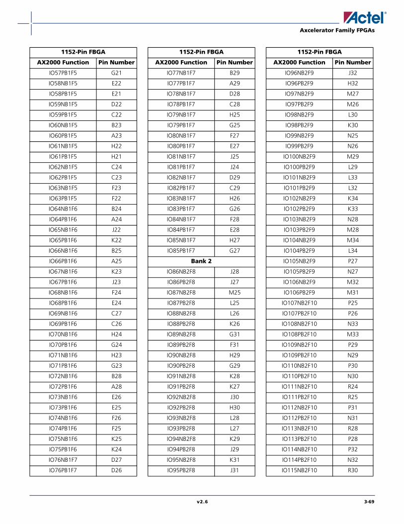
Axcelerator Family FPGAs
v2.6 3-69
IO57PB1F5 G21
IO58NB1F5 E22
IO58PB1F5 E21
IO59NB1F5 D22
IO59PB1F5 C22
IO60NB1F5 B23
IO60PB1F5 A23
IO61NB1F5 H22
IO61PB1F5 H21
IO62NB1F5 C24
IO62PB1F5 C23
IO63NB1F5 F23
IO63PB1F5 F22
IO64NB1F6 B24
IO64PB1F6 A24
IO65NB1F6 J22
IO65PB1F6 K22
IO66NB1F6 B25
IO66PB1F6 A25
IO67NB1F6 K23
IO67PB1F6 J23
IO68NB1F6 F24
IO68PB1F6 E24
IO69NB1F6 C27
IO69PB1F6 C26
IO70NB1F6 H24
IO70PB1F6 G24
IO71NB1F6 H23
IO71PB1F6 G23
IO72NB1F6 B28
IO72PB1F6 A28
IO73NB1F6 E26
IO73PB1F6 E25
IO74NB1F6 F26
IO74PB1F6 F25
IO75NB1F6 K25
IO75PB1F6 K24
IO76NB1F7 D27
IO76PB1F7 D26
1152-Pin FBGA
AX2000 Function Pin Number
IO77NB1F7 B29
IO77PB1F7 A29
IO78NB1F7 D28
IO78PB1F7 C28
IO79NB1F7 H25
IO79PB1F7 G25
IO80NB1F7 F27
IO80PB1F7 E27
IO81NB1F7 J25
IO81PB1F7 J24
IO82NB1F7 D29
IO82PB1F7 C29
IO83NB1F7 H26
IO83PB1F7 G26
IO84NB1F7 F28
IO84PB1F7 E28
IO85NB1F7 H27
IO85PB1F7 G27
Bank 2
IO86NB2F8 J28
IO86PB2F8 J27
IO87NB2F8 M25
IO87PB2F8 L25
IO88NB2F8 L26
IO88PB2F8 K26
IO89NB2F8 G31
IO89PB2F8 F31
IO90NB2F8 H29
IO90PB2F8 G29
IO91NB2F8 K28
IO91PB2F8 K27
IO92NB2F8 J30
IO92PB2F8 H30
IO93NB2F8 L28
IO93PB2F8 L27
IO94NB2F8 K29
IO94PB2F8 J29
IO95NB2F8 K31
IO95PB2F8 J31
1152-Pin FBGA
AX2000 Function Pin Number
IO96NB2F9 J32
IO96PB2F9 H32
IO97NB2F9 M27
IO97PB2F9 M26
IO98NB2F9 L30
IO98PB2F9 K30
IO99NB2F9 N25
IO99PB2F9 N26
IO100NB2F9 M29
IO100PB2F9 L29
IO101NB2F9 L33
IO101PB2F9 L32
IO102NB2F9 K34
IO102PB2F9 K33
IO103NB2F9 N28
IO103PB2F9 M28
IO104NB2F9 M34
IO104PB2F9 L34
IO105NB2F9 P27
IO105PB2F9 N27
IO106NB2F9 M32
IO106PB2F9 M31
IO107NB2F10 P25
IO107PB2F10 P26
IO108NB2F10 N33
IO108PB2F10 M33
IO109NB2F10 P29
IO109PB2F10 N29
IO110NB2F10 P30
IO110PB2F10 N30
IO111NB2F10 R24
IO111PB2F10 R25
IO112NB2F10 P31
IO112PB2F10 N31
IO113NB2F10 R28
IO113PB2F10 P28
IO114NB2F10 P32
IO114PB2F10 N32
IO115NB2F10 R30
1152-Pin FBGA
AX2000 Function Pin Number

Axcelerator Family FPGAs
3-70 v2.6
IO115PB2F10 R29
IO116NB2F10 P34
IO116PB2F10 P33
IO117NB2F10 R27
IO117PB2F10 R26
IO118NB2F11 R34
IO118PB2F11 R33
IO119NB2F11 T24
IO119PB2F11 T25
IO120NB2F11 T33
IO120PB2F11 T34
IO121NB2F11 T27
IO121PB2F11 T26
IO122NB2F11 T30
IO122PB2F11 T29
IO123NB2F11 U28
IO123PB2F11 T28
IO124NB2F11 T31
IO124PB2F11 T32
IO125NB2F11 U24
IO125PB2F11 U25
IO126NB2F11 U33
IO126PB2F11 U34
IO127NB2F11 U26
IO127PB2F11 U27
IO128NB2F11 U31
IO128PB2F11 U32
Bank 3
IO129NB3F12 V29
IO129PB3F12 U29
IO130NB3F12 V31
IO130PB3F12 V32
IO131NB3F12 V24
IO131PB3F12 V25
IO132NB3F12 W28
IO132PB3F12 V28
IO133NB3F12 W26
IO133PB3F12 V26
IO134NB3F12 W33
1152-Pin FBGA
AX2000 Function Pin Number
IO134PB3F12 V33
IO135NB3F12 W25
IO135PB3F12 W24
IO136NB3F12 W31
IO136PB3F12 W32
IO137NB3F12 Y30
IO137PB3F12 W30
IO138NB3F12 Y29
IO138PB3F12 W29
IO139NB3F13 Y27
IO139PB3F13 W27
IO140NB3F13 AA33
IO140PB3F13 Y33
IO141NB3F13 Y25
IO141PB3F13 Y24
IO142NB3F13 AA31
IO142PB3F13 Y31
IO143NB3F13 AA28
IO143PB3F13 Y28
IO144NB3F13 AA34
IO144PB3F13 Y34
IO145NB3F13 AA26
IO145PB3F13 Y26
IO146NB3F13 AA29
IO146PB3F13 AA30
IO147NB3F13 AB30
IO147PB3F13 AB29
IO148NB3F13 AB32
IO148PB3F13 AA32
IO149NB3F13 AB27
IO149PB3F13 AA27
IO150NB3F14 AC31
IO150PB3F14 AB31
IO151NB3F14 AD33
IO151PB3F14 AC33
IO152NB3F14 AC28
IO152PB3F14 AB28
IO153NB3F14 AB25
IO153PB3F14 AA25
1152-Pin FBGA
AX2000 Function Pin Number
IO154NB3F14 AD32
IO154PB3F14 AC32
IO155NB3F14 AD29
IO155PB3F14 AC29
IO156NB3F14 AE30
IO156PB3F14 AD30
IO157NB3F14 AC26
IO157PB3F14 AB26
IO158NB3F14 AH33
IO158PB3F14 AG33
IO159NB3F14 AD27
IO159PB3F14 AC27
IO160NB3F14 AG32
IO160PB3F14 AF32
IO161NB3F15 AG31
IO161PB3F15 AF31
IO162NB3F15 AF29
IO162PB3F15 AE29
IO163NB3F15 AE28
IO163PB3F15 AD28
IO164NB3F15 AG30
IO164PB3F15 AF30
IO165NB3F15 AE26
IO165PB3F15 AD26
IO166NB3F15 AJ30
IO166PB3F15 AH30
IO167NB3F15 AG28
IO167PB3F15 AF28
IO168NB3F15 AF27
IO168PB3F15 AE27
IO169NB3F15 AH29
IO169PB3F15 AG29
IO170NB3F15 AD25
IO170PB3F15 AC25
Bank 4
IO171NB4F16 AP29
IO171PB4F16 AN29
IO172NB4F16 AH26
IO172PB4F16 AH27
1152-Pin FBGA
AX2000 Function Pin Number

Axcelerator Family FPGAs
v2.6 3-71
IO173NB4F16 AJ27
IO173PB4F16 AJ28
IO174NB4F16 AL27
IO174PB4F16 AL28
IO175NB4F16 AM28
IO175PB4F16 AM29
IO176NB4F16 AG25
IO176PB4F16 AG26
IO177NB4F16 AK26
IO177PB4F16 AK27
IO178NB4F16 AF25
IO178PB4F16 AE25
IO179NB4F16 AP28
IO179PB4F16 AN28
IO180NB4F16 AJ25
IO180PB4F16 AJ26
IO181NB4F17 AM26
IO181PB4F17 AM27
IO182NB4F17 AF24
IO182PB4F17 AE24
IO183NB4F17 AH24
IO183PB4F17 AH25
IO184NB4F17 AG23
IO184PB4F17 AG24
IO185NB4F17 AL25
IO185PB4F17 AL26
IO186NB4F17 AP25
IO186PB4F17 AP26
IO187NB4F17 AK24
IO187PB4F17 AK25
IO188NB4F17 AF23
IO188PB4F17 AE23
IO189NB4F17 AN24
IO189PB4F17 AM24
IO190NB4F17 AH22
IO190PB4F17 AH23
IO191NB4F17 AJ23
IO191PB4F17 AJ24
IO192NB4F17 AG21
1152-Pin FBGA
AX2000 Function Pin Number
IO192PB4F17 AG22
IO193NB4F18 AP23
IO193PB4F18 AP24
IO194NB4F18 AN22
IO194PB4F18 AN23
IO195NB4F18 AM23
IO195PB4F18 AL23
IO196NB4F18 AF21
IO196PB4F18 AF22
IO197NB4F18 AL22
IO197PB4F18 AM22
IO198NB4F18 AE21
IO198PB4F18 AE22
IO199NB4F18 AJ21
IO199PB4F18 AJ22
IO200NB4F18 AK21
IO200PB4F18 AK22
IO201NB4F18 AM21
IO201PB4F18 AL21
IO202NB4F18 AE20
IO202PB4F18 AD20
IO203NB4F19 AN21
IO203PB4F19 AP21
IO204NB4F19 AP20
IO204PB4F19 AN20
IO205NB4F19 AN19
IO205PB4F19 AP19
IO206NB4F19 AG20
IO206PB4F19 AF20
IO207NB4F19 AL19
IO207PB4F19 AL20
IO208NB4F19 AG19
IO208PB4F19 AF19
IO209NB4F19 AN18
IO209PB4F19 AP18
IO210NB4F19 AE19
IO210PB4F19 AD19
IO211NB4F19 AL18
IO211PB4F19 AM18
1152-Pin FBGA
AX2000 Function Pin Number
IO212NB4F19/CLKEN AJ20
IO212PB4F19/CLKEP AK20
IO213NB4F19/CLKFN AJ18
IO213PB4F19/CLKFP AJ19
Bank 5
IO214NB5F20/CLKGN AJ16
IO214PB5F20/CLKGP AJ17
IO215NB5F20/CLKHN AJ15
IO215PB5F20/CLKHP AK15
IO216NB5F20 AD16
IO216PB5F20 AE17
IO217NB5F20 AM17
IO217PB5F20 AL17
IO218NB5F20 AG16
IO218PB5F20 AF16
IO219NB5F20 AM16
IO219PB5F20 AL16
IO220NB5F20 AP16
IO220PB5F20 AN16
IO221NB5F20 AN15
IO221PB5F20 AP15
IO222NB5F20 AD15
IO222PB5F20 AE16
IO223NB5F21 AL14
IO223PB5F21 AL15
IO224NB5F21 AN14
IO224PB5F21 AP14
IO225NB5F21 AK13
IO225PB5F21 AK14
IO226NB5F21 AE15
IO226PB5F21 AF15
IO227NB5F21 AG14
IO227PB5F21 AG15
IO228NB5F21 AJ13
IO228PB5F21 AJ14
IO229NB5F21 AM13
IO229PB5F21 AM14
IO230NB5F21 AE14
IO230PB5F21 AF14
1152-Pin FBGA
AX2000 Function Pin Number
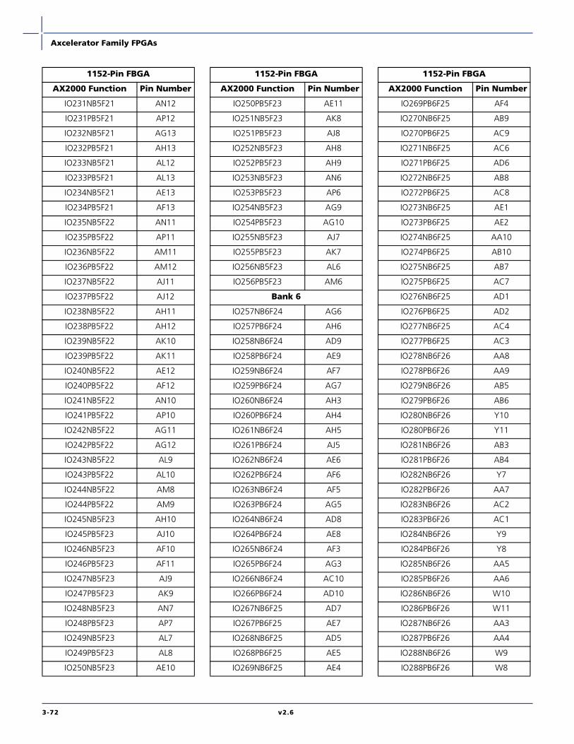
Axcelerator Family FPGAs
3-72 v2.6
IO231NB5F21 AN12
IO231PB5F21 AP12
IO232NB5F21 AG13
IO232PB5F21 AH13
IO233NB5F21 AL12
IO233PB5F21 AL13
IO234NB5F21 AE13
IO234PB5F21 AF13
IO235NB5F22 AN11
IO235PB5F22 AP11
IO236NB5F22 AM11
IO236PB5F22 AM12
IO237NB5F22 AJ11
IO237PB5F22 AJ12
IO238NB5F22 AH11
IO238PB5F22 AH12
IO239NB5F22 AK10
IO239PB5F22 AK11
IO240NB5F22 AE12
IO240PB5F22 AF12
IO241NB5F22 AN10
IO241PB5F22 AP10
IO242NB5F22 AG11
IO242PB5F22 AG12
IO243NB5F22 AL9
IO243PB5F22 AL10
IO244NB5F22 AM8
IO244PB5F22 AM9
IO245NB5F23 AH10
IO245PB5F23 AJ10
IO246NB5F23 AF10
IO246PB5F23 AF11
IO247NB5F23 AJ9
IO247PB5F23 AK9
IO248NB5F23 AN7
IO248PB5F23 AP7
IO249NB5F23 AL7
IO249PB5F23 AL8
IO250NB5F23 AE10
1152-Pin FBGA
AX2000 Function Pin Number
IO250PB5F23 AE11
IO251NB5F23 AK8
IO251PB5F23 AJ8
IO252NB5F23 AH8
IO252PB5F23 AH9
IO253NB5F23 AN6
IO253PB5F23 AP6
IO254NB5F23 AG9
IO254PB5F23 AG10
IO255NB5F23 AJ7
IO255PB5F23 AK7
IO256NB5F23 AL6
IO256PB5F23 AM6
Bank 6
IO257NB6F24 AG6
IO257PB6F24 AH6
IO258NB6F24 AD9
IO258PB6F24 AE9
IO259NB6F24 AF7
IO259PB6F24 AG7
IO260NB6F24 AH3
IO260PB6F24 AH4
IO261NB6F24 AH5
IO261PB6F24 AJ5
IO262NB6F24 AE6
IO262PB6F24 AF6
IO263NB6F24 AF5
IO263PB6F24 AG5
IO264NB6F24 AD8
IO264PB6F24 AE8
IO265NB6F24 AF3
IO265PB6F24 AG3
IO266NB6F24 AC10
IO266PB6F24 AD10
IO267NB6F25 AD7
IO267PB6F25 AE7
IO268NB6F25 AD5
IO268PB6F25 AE5
IO269NB6F25 AE4
1152-Pin FBGA
AX2000 Function Pin Number
IO269PB6F25 AF4
IO270NB6F25 AB9
IO270PB6F25 AC9
IO271NB6F25 AC6
IO271PB6F25 AD6
IO272NB6F25 AB8
IO272PB6F25 AC8
IO273NB6F25 AE1
IO273PB6F25 AE2
IO274NB6F25 AA10
IO274PB6F25 AB10
IO275NB6F25 AB7
IO275PB6F25 AC7
IO276NB6F25 AD1
IO276PB6F25 AD2
IO277NB6F25 AC4
IO277PB6F25 AC3
IO278NB6F26 AA8
IO278PB6F26 AA9
IO279NB6F26 AB5
IO279PB6F26 AB6
IO280NB6F26 Y10
IO280PB6F26 Y11
IO281NB6F26 AB3
IO281PB6F26 AB4
IO282NB6F26 Y7
IO282PB6F26 AA7
IO283NB6F26 AC2
IO283PB6F26 AC1
IO284NB6F26 Y9
IO284PB6F26 Y8
IO285NB6F26 AA5
IO285PB6F26 AA6
IO286NB6F26 W10
IO286PB6F26 W11
IO287NB6F26 AA3
IO287PB6F26 AA4
IO288NB6F26 W9
IO288PB6F26 W8
1152-Pin FBGA
AX2000 Function Pin Number

Axcelerator Family FPGAs
v2.6 3-73
IO289NB6F27 AA1
IO289PB6F27 AA2
IO290NB6F27 W6
IO290PB6F27 Y6
IO291NB6F27 W5
IO291PB6F27 Y5
IO292NB6F27 V7
IO292PB6F27 W7
IO293NB6F27 W4
IO293PB6F27 Y4
IO294NB6F27 V10
IO294PB6F27 V11
IO295NB6F27 Y1
IO295PB6F27 Y2
IO296NB6F27 W1
IO296PB6F27 W2
IO297NB6F27 V1
IO297PB6F27 V2
IO298NB6F27 V9
IO298PB6F27 V8
IO299NB6F27 U4
IO299PB6F27 V4
Bank 7
IO300NB7F28 U10
IO300PB7F28 U11
IO301NB7F28 U2
IO301PB7F28 U1
IO302NB7F28 U6
IO302PB7F28 U7
IO303NB7F28 T3
IO303PB7F28 U3
IO304NB7F28 U9
IO304PB7F28 U8
IO305NB7F28 R2
IO305PB7F28 R1
IO306NB7F28 R4
IO306PB7F28 T4
IO307NB7F28 R5
IO307PB7F28 T5
1152-Pin FBGA
AX2000 Function Pin Number
IO308NB7F28 T11
IO308PB7F28 T10
IO309NB7F28 T6
IO309PB7F28 T7
IO310NB7F29 T9
IO310PB7F29 T8
IO311NB7F29 N3
IO311PB7F29 P3
IO312NB7F29 P7
IO312PB7F29 R7
IO313NB7F29 P6
IO313PB7F29 R6
IO314NB7F29 M2
IO314PB7F29 N2
IO315NB7F29 N4
IO315PB7F29 P4
IO316NB7F29 R9
IO316PB7F29 R8
IO317NB7F29 N5
IO317PB7F29 P5
IO318NB7F29 R10
IO318PB7F29 R11
IO319NB7F29 L2
IO319PB7F29 L1
IO320NB7F29 N8
IO320PB7F29 P8
IO321NB7F30 M6
IO321PB7F30 N6
IO322NB7F30 P10
IO322PB7F30 P9
IO323NB7F30 L3
IO323PB7F30 M3
IO324NB7F30 M7
IO324PB7F30 N7
IO325NB7F30 K2
IO325PB7F30 K1
IO326NB7F30 G2
IO326PB7F30 H2
IO327NB7F30 L6
1152-Pin FBGA
AX2000 Function Pin Number
IO327PB7F30 L5
IO328NB7F30 N10
IO328PB7F30 N9
IO329NB7F30 J4
IO329PB7F30 K4
IO330NB7F30 J5
IO330PB7F30 K5
IO331NB7F30 M10
IO331PB7F30 M9
IO332NB7F31 L8
IO332PB7F31 M8
IO333NB7F31 F2
IO333PB7F31 F1
IO334NB7F31 J6
IO334PB7F31 K6
IO335NB7F31 H4
IO335PB7F31 H3
IO336NB7F31 K7
IO336PB7F31 L7
IO337NB7F31 G4
IO337PB7F31 G3
IO338NB7F31 K9
IO338PB7F31 L9
IO339NB7F31 H6
IO339PB7F31 H5
IO340NB7F31 H7
IO340PB7F31 J7
IO341NB7F31 J8
IO341PB7F31 K8
Dedicated I/O
GND A13
GND A2
GND A22
GND A27
GND A3
GND A31
GND A32
GND A33
GND A4
1152-Pin FBGA
AX2000 Function Pin Number

Axcelerator Family FPGAs
3-74 v2.6
GND A8
GND AA14
GND AA15
GND AA16
GND AA17
GND AA18
GND AA19
GND AA20
GND AA21
GND AB1
GND AB13
GND AB22
GND AB34
GND AC12
GND AC23
GND AC30
GND AC5
GND AD11
GND AD24
GND AD31
GND AD4
GND AE3
GND AE32
GND AF2
GND AF33
GND AG1
GND AG27
GND AG34
GND AG8
GND AH28
GND AH7
GND AJ29
GND AJ6
GND AK12
GND AK17
GND AK18
GND AK23
GND AK30
GND AK5
1152-Pin FBGA
AX2000 Function Pin Number
GND AL1
GND AL11
GND AL2
GND AL24
GND AL3
GND AL31
GND AL32
GND AL33
GND AL34
GND AL4
GND AM1
GND AM10
GND AM15
GND AM2
GND AM20
GND AM25
GND AM3
GND AM31
GND AM32
GND AM33
GND AM34
GND AM4
GND AN1
GND AN2
GND AN26
GND AN3
GND AN31
GND AN32
GND AN33
GND AN34
GND AN4
GND AN9
GND AP13
GND AP2
GND AP22
GND AP27
GND AP3
GND AP31
GND AP32
1152-Pin FBGA
AX2000 Function Pin Number
GND AP33
GND AP4
GND AP8
GND B1
GND B2
GND B26
GND B3
GND B31
GND B32
GND B33
GND B34
GND B4
GND B9
GND C1
GND C10
GND C15
GND C2
GND C20
GND C25
GND C3
GND C31
GND C32
GND C33
GND C34
GND C4
GND D1
GND D11
GND D2
GND D24
GND D3
GND D31
GND D32
GND D33
GND D34
GND D4
GND E12
GND E17
GND E18
GND E23
1152-Pin FBGA
AX2000 Function Pin Number

Axcelerator Family FPGAs
v2.6 3-75
GND E30
GND E5
GND F29
GND F30
GND F6
GND G28
GND G7
GND H1
GND H34
GND J2
GND J33
GND K3
GND K32
GND L11
GND L24
GND L31
GND L4
GND M12
GND M23
GND M30
GND M5
GND N1
GND N13
GND N22
GND N34
GND P14
GND P15
GND P16
GND P17
GND P18
GND P19
GND P20
GND P21
GND R14
GND R15
GND R16
GND R17
GND R18
GND R19
1152-Pin FBGA
AX2000 Function Pin Number
GND R20
GND R21
GND R3
GND R32
GND T14
GND T15
GND T16
GND T17
GND T18
GND T19
GND T20
GND T21
GND U14
GND U15
GND U16
GND U17
GND U18
GND U19
GND U20
GND U21
GND U30
GND U5
GND V14
GND V15
GND V16
GND V17
GND V18
GND V19
GND V20
GND V21
GND V30
GND V5
GND W14
GND W15
GND W16
GND W17
GND W18
GND W19
GND W20
1152-Pin FBGA
AX2000 Function Pin Number
GND W21
GND Y14
GND Y15
GND Y16
GND Y17
GND Y18
GND Y19
GND Y20
GND Y21
GND Y3
GND Y32
GND/LP G6
NC A17
NC A26
NC AB2
NC AB33
NC AC34
NC AD3
NC AD34
NC AE31
NC AE33
NC AE34
NC AF1
NC AF34
NC AG2
NC AG4
NC AH1
NC AH2
NC AH31
NC AH32
NC AH34
NC AJ1
NC AJ2
NC AJ3
NC AJ31
NC AJ32
NC AJ33
NC AJ34
NC AJ4
1152-Pin FBGA
AX2000 Function Pin Number
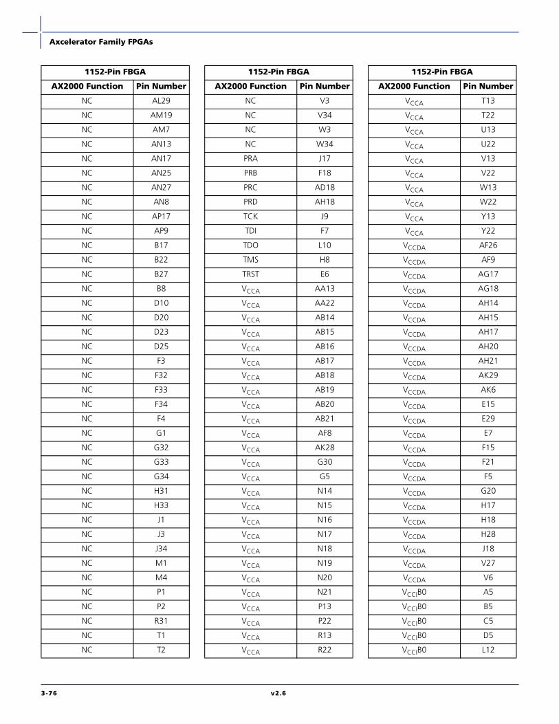
Axcelerator Family FPGAs
3-76 v2.6
NC AL29
NC AM19
NC AM7
NC AN13
NC AN17
NC AN25
NC AN27
NC AN8
NC AP17
NC AP9
NC B17
NC B22
NC B27
NC B8
NC D10
NC D20
NC D23
NC D25
NC F3
NC F32
NC F33
NC F34
NC F4
NC G1
NC G32
NC G33
NC G34
NC H31
NC H33
NC J1
NC J3
NC J34
NC M1
NC M4
NC P1
NC P2
NC R31
NC T1
NC T2
1152-Pin FBGA
AX2000 Function Pin Number
NC V3
NC V34
NC W3
NC W34
PRA J17
PRB F18
PRC AD18
PRD AH18
TCK J9
TDI F7
TDO L10
TMS H8
TRST E6
VCCA AA13
VCCA AA22
VCCA AB14
VCCA AB15
VCCA AB16
VCCA AB17
VCCA AB18
VCCA AB19
VCCA AB20
VCCA AB21
VCCA AF8
VCCA AK28
VCCA G30
VCCA G5
VCCA N14
VCCA N15
VCCA N16
VCCA N17
VCCA N18
VCCA N19
VCCA N20
VCCA N21
VCCA P13
VCCA P22
VCCA R13
VCCA R22
1152-Pin FBGA
AX2000 Function Pin Number
VCCA T13
VCCA T22
VCCA U13
VCCA U22
VCCA V13
VCCA V22
VCCA W13
VCCA W22
VCCA Y13
VCCA Y22
VCCDA AF26
VCCDA AF9
VCCDA AG17
VCCDA AG18
VCCDA AH14
VCCDA AH15
VCCDA AH17
VCCDA AH20
VCCDA AH21
VCCDA AK29
VCCDA AK6
VCCDA E15
VCCDA E29
VCCDA E7
VCCDA F15
VCCDA F21
VCCDA F5
VCCDA G20
VCCDA H17
VCCDA H18
VCCDA H28
VCCDA J18
VCCDA V27
VCCDA V6
VCCIB0 A5
VCCIB0 B5
VCCIB0 C5
VCCIB0 D5
VCCIB0 L12
1152-Pin FBGA
AX2000 Function Pin Number

Axcelerator Family FPGAs
v2.6 3-77
VCCIB0 L13
VCCIB0 L14
VCCIB0 M13
VCCIB0 M14
VCCIB0 M15
VCCIB0 M16
VCCIB0 M17
VCCIB1 A30
VCCIB1 B30
VCCIB1 C30
VCCIB1 D30
VCCIB1 L21
VCCIB1 L22
VCCIB1 L23
VCCIB1 M18
VCCIB1 M19
VCCIB1 M20
VCCIB1 M21
VCCIB1 M22
VCCIB2 E31
VCCIB2 E32
VCCIB2 E33
VCCIB2 E34
VCCIB2 M24
VCCIB2 N23
VCCIB2 N24
VCCIB2 P23
VCCIB2 P24
VCCIB2 R23
VCCIB2 T23
VCCIB2 U23
VCCIB3 AA23
VCCIB3 AA24
VCCIB3 AB23
VCCIB3 AB24
VCCIB3 AC24
VCCIB3 AK31
VCCIB3 AK32
VCCIB3 AK33
1152-Pin FBGA
AX2000 Function Pin Number
VCCIB3 AK34
VCCIB3 V23
VCCIB3 W23
VCCIB3 Y23
VCCIB4 AC18
VCCIB4 AC19
VCCIB4 AC20
VCCIB4 AC21
VCCIB4 AC22
VCCIB4 AD21
VCCIB4 AD22
VCCIB4 AD23
VCCIB4 AL30
VCCIB4 AM30
VCCIB4 AN30
VCCIB4 AP30
VCCIB5 AC13
VCCIB5 AC14
VCCIB5 AC15
VCCIB5 AC16
VCCIB5 AC17
VCCIB5 AD12
VCCIB5 AD13
VCCIB5 AD14
VCCIB5 AL5
VCCIB5 AM5
VCCIB5 AN5
VCCIB5 AP5
VCCIB6 AA11
VCCIB6 AA12
VCCIB6 AB11
VCCIB6 AB12
VCCIB6 AC11
VCCIB6 AK1
VCCIB6 AK2
VCCIB6 AK3
VCCIB6 AK4
VCCIB6 V12
VCCIB6 W12
1152-Pin FBGA
AX2000 Function Pin Number
VCCIB6 Y12
VCCIB7 E1
VCCIB7 E2
VCCIB7 E3
VCCIB7 E4
VCCIB7 M11
VCCIB7 N11
VCCIB7 N12
VCCIB7 P11
VCCIB7 P12
VCCIB7 R12
VCCIB7 T12
VCCIB7 U12
VCCPLA J16
VCCPLB K17
VCCPLC J19
VCCPLD L18
VCCPLE AK19
VCCPLF AE18
VCCPLG AK16
VCCPLH AF17
VCOMPLA H16
VCOMPLB L17
VCOMPLC H19
VCOMPLD K18
VCOMPLE AH19
VCOMPLF AF18
VCOMPLG AH16
VCOMPLH AD17
VPUMP J26
1152-Pin FBGA
AX2000 Function Pin Number

Axcelerator Family FPGAs
3-78 v2.6
208-Pin PQFP
NoteFor Package Manufacturing and Environmental information, visit Resource center athttp://www.actel.com/products/rescenter/package/index.html.
Figure 3-9 • 208-Pin PQFP
208-Pin PQFP
1208

Axcelerator Family FPGAs
v2.6 3-79
208-Pin PQFP
AX250 Function Pin Number
Bank 0
IO02NB0F0 197
IO03NB0F0 198
IO03PB0F0 199
IO12NB0F0/HCLKAN 191
IO12PB0F0/HCLKAP 192
IO13NB0F0/HCLKBN 185
IO13PB0F0/HCLKBP 186
Bank 1
IO14NB1F1/HCLKCN 180
IO14PB1F1/HCLKCP 181
IO15NB1F1/HCLKDN 174
IO15PB1F1/HCLKDP 175
IO16NB1F1 170
IO16PB1F1 171
IO24NB1F1 165
IO24PB1F1 166
IO26NB1F1 161
IO26PB1F1 162
IO27NB1F1 159
IO27PB1F1 160
Bank 2
IO29NB2F2 151
IO29PB2F2 153
IO30NB2F2 152
IO30PB2F2 154
IO31PB2F2 148
IO32NB2F2 146
IO32PB2F2 147
IO34NB2F2 144
IO34PB2F2 145
IO39NB2F2 139
IO39PB2F2 140
IO40PB2F2 141
IO41NB2F2 137
IO41PB2F2 138
IO43NB2F2 132
IO43PB2F2 134
IO44NB2F2 131
IO44PB2F2 133
Bank 3
IO45NB3F3 127
IO45PB3F3 129
IO46NB3F3 126
IO46PB3F3 128
IO48NB3F3 122
IO48PB3F3 123
IO50NB3F3 120
IO50PB3F3 121
IO55NB3F3 116
IO55PB3F3 117
IO57NB3F3 114
IO57PB3F3 115
IO59NB3F3 110
IO59PB3F3 111
IO60NB3F3 108
IO60PB3F3 109
IO61NB3F3 106
IO61PB3F3 107
Bank 4
IO62NB4F4 100
IO62PB4F4 103
IO63NB4F4 101
IO63PB4F4 102
IO64NB4F4 96
IO64PB4F4 97
IO72NB4F4 91
IO72PB4F4 92
IO74NB4F4/CLKEN 87
IO74PB4F4/CLKEP 88
IO75NB4F4/CLKFN 81
IO75PB4F4/CLKFP 82
Bank 5
IO76NB5F5/CLKGN 76
IO76PB5F5/CLKGP 77
IO77NB5F5/CLKHN 70
208-Pin PQFP
AX250 Function Pin Number
IO77PB5F5/CLKHP 71
IO78NB5F5 66
IO78PB5F5 67
IO86NB5F5 62
IO87NB5F5 60
IO87PB5F5 61
IO88NB5F5 56
IO88PB5F5 57
IO89NB5F5 54
IO89PB5F5 55
Bank 6
IO91NB6F6 47
IO91PB6F6 49
IO92NB6F6 48
IO92PB6F6 50
IO93NB6F6 42
IO93PB6F6 43
IO94PB6F6 44
IO96NB6F6 40
IO96PB6F6 41
IO101NB6F6 35
IO101PB6F6 36
IO102PB6F6 37
IO103NB6F6 33
IO103PB6F6 34
IO105NB6F6 28
IO105PB6F6 30
IO106NB6F6 27
IO106PB6F6 29
Bank 7
IO107NB7F7 23
IO107PB7F7 25
IO108NB7F7 22
IO108PB7F7 24
IO110NB7F7 18
IO110PB7F7 19
IO112NB7F7 16
IO112PB7F7 17
208-Pin PQFP
AX250 Function Pin Number

Axcelerator Family FPGAs
3-80 v2.6
IO117NB7F7 12
IO117PB7F7 13
IO119NB7F7 10
IO119PB7F7 11
IO121PB7F7 7
IO122NB7F7 5
IO122PB7F7 6
IO123NB7F7 3
IO123PB7F7 4
Dedicated I/O
VCCDA 1
VCCDA 26
VCCDA 53
VCCDA 63
VCCDA 78
VCCDA 95
VCCDA 105
VCCDA 130
VCCDA 157
VCCDA 167
VCCDA 182
VCCDA 202
GND 104
GND 9
GND 15
GND 21
GND 32
GND 39
GND 46
GND 51
GND 59
GND 65
GND 69
GND 90
GND 94
GND 99
GND 113
GND 119
208-Pin PQFP
AX250 Function Pin Number
GND 125
GND 136
GND 143
GND 150
GND 155
GND 164
GND 169
GND 173
GND 194
GND 196
GND 201
GND/LP 208
PRA 184
PRB 183
PRC 80
PRD 79
TCK 205
TDI 204
TDO 203
TMS 206
TRST 207
VCCA 2
VCCA 52
VCCA 156
VCCA 14
VCCA 38
VCCA 64
VCCA 93
VCCA 118
VCCA 142
VCCA 168
VCCA 195
VCCPLA 189
VCCPLB 187
VCCPLC 178
VCCPLD 176
VCCPLE 85
VCCPLF 83
208-Pin PQFP
AX250 Function Pin Number
VCCPLG 74
VCCPLH 72
VCCIB0 193
VCCIB0 200
VCCIB1 163
VCCIB1 172
VCCIB2 135
VCCIB2 149
VCCIB3 112
VCCIB3 124
VCCIB4 89
VCCIB4 98
VCCIB5 58
VCCIB5 68
VCCIB6 31
VCCIB6 45
VCCIB7 8
VCCIB7 20
VCOMPLA 190
VCOMPLB 188
VCOMPLC 179
VCOMPLD 177
VCOMPLE 86
VCOMPLF 84
VCOMPLG 75
VCOMPLH 73
VPUMP 158
208-Pin PQFP
AX250 Function Pin Number

Axcelerator Family FPGAs
v2.6 3-81
208-Pin PQFP
AX500 Function Pin Number
Bank 0
IO03NB0F0 198
IO03PB0F0 199
IO04NB0F0 197
IO19NB0F1/HCLKAN 191
IO19PB0F1/HCLKAP 192
IO20NB0F1/HCLKBN 185
IO20PB0F1/HCLKBP 186
Bank 1
IO21NB1F2/HCLKCN 180
IO21PB1F2/HCLKCP 181
IO22NB1F2/HCLKDN 174
IO22PB1F2/HCLKDP 175
IO23NB1F2 170
IO23PB1F2 171
IO37NB1F3 165
IO37PB1F3 166
IO39NB1F3 161
IO39PB1F3 162
IO41NB1F3 159
IO41PB1F3 160
Bank 2
IO43NB2F4 151
IO43PB2F4 153
IO44NB2F4 152
IO44PB2F4 154
IO45PB2F4 148
IO46NB2F4 146
IO46PB2F4 147
IO48NB2F4 144
IO48PB2F4 145
IO57NB2F5 139
IO57PB2F5 140
IO58PB2F5 141
IO59NB2F5 137
IO59PB2F5 138
IO61NB2F5 132
IO61PB2F5 134
IO62NB2F5 131
IO62PB2F5 133
Bank 3
IO63NB3F6 127
IO63PB3F6 129
IO64NB3F6 126
IO64PB3F6 128
IO66NB3F6 122
IO66PB3F6 123
IO68NB3F6 120
IO68PB3F6 121
IO77NB3F7 116
IO77PB3F7 117
IO79NB3F7 114
IO79PB3F7 115
IO81NB3F7 110
IO81PB3F7 111
IO82NB3F7 108
IO82PB3F7 109
IO83NB3F7 106
IO83PB3F7 107
Bank 4
IO84PB4F8 103
IO85NB4F8 100
IO86NB4F8 101
IO86PB4F8 102
IO87NB4F8 96
IO87PB4F8 97
IO101NB4F9 91
IO101PB4F9 92
IO103NB4F9/CLKEN 87
IO103PB4F9/CLKEP 88
IO104NB4F9/CLKFN 81
IO104PB4F9/CLKFP 82
Bank 5
IO105NB5F10/CLKGN 76
IO105PB5F10/CLKGP 77
IO106NB5F10/CLKHN 70
208-Pin PQFP
AX500 Function Pin Number
IO106PB5F10/CLKHP 71
IO107NB5F10 66
IO107PB5F10 67
IO119NB5F11 62
IO121NB5F11 60
IO121PB5F11 61
IO123NB5F11 56
IO123PB5F11 57
IO125NB5F11 54
IO125PB5F11 55
Bank 6
IO127NB6F12 47
IO127PB6F12 49
IO128NB6F12 48
IO128PB6F12 50
IO129NB6F12 42
IO129PB6F12 43
IO130PB6F12 44
IO132NB6F12 40
IO132PB6F12 41
IO141NB6F13 35
IO141PB6F13 36
IO142PB6F13 37
IO143NB6F13 33
IO143PB6F13 34
IO145NB6F13 28
IO145PB6F13 30
IO146NB6F13 27
IO146PB6F13 29
Bank 7
IO147NB7F14 23
IO147PB7F14 25
IO148NB7F14 22
IO148PB7F14 24
IO150NB7F14 18
IO150PB7F14 19
IO152NB7F14 16
IO152PB7F14 17
208-Pin PQFP
AX500 Function Pin Number

Axcelerator Family FPGAs
3-82 v2.6
IO161NB7F15 12
IO161PB7F15 13
IO163NB7F15 10
IO163PB7F15 11
IO165PB7F15 7
IO166NB7F15 5
IO166PB7F15 6
IO167NB7F15 3
IO167PB7F15 4
Dedicated I/O
VCCDA 1
VCCDA 26
VCCDA 53
VCCDA 63
VCCDA 78
VCCDA 95
VCCDA 105
VCCDA 130
VCCDA 157
VCCDA 167
VCCDA 182
VCCDA 202
GND 104
GND 9
GND 15
GND 21
GND 32
GND 39
GND 46
GND 51
GND 59
GND 65
GND 69
GND 90
GND 94
GND 99
GND 113
GND 119
208-Pin PQFP
AX500 Function Pin Number
GND 125
GND 143
GND 136
GND 150
GND 155
GND 164
GND 169
GND 173
GND 194
GND 196
GND 201
GND/LP 208
PRA 184
PRB 183
PRC 80
PRD 79
TCK 205
TDI 204
TDO 203
TMS 206
TRST 207
VCCA 2
VCCA 14
VCCA 38
VCCA 52
VCCA 64
VCCA 93
VCCA 118
VCCA 142
VCCA 156
VCCA 168
VCCA 195
VCCPLA 189
VCCPLB 187
VCCPLC 178
VCCPLD 176
VCCPLE 85
VCCPLF 83
208-Pin PQFP
AX500 Function Pin Number
VCCPLG 74
VCCPLH 72
VCCIB0 200
VCCIB0 193
VCCIB1 172
VCCIB1 163
VCCIB2 149
VCCIB2 135
VCCIB3 124
VCCIB3 112
VCCIB4 98
VCCIB4 89
VCCIB5 68
VCCIB5 58
VCCIB6 45
VCCIB6 31
VCCIB7 20
VCCIB7 8
VCOMPLA 190
VCOMPLB 188
VCOMPLC 179
VCOMPLD 177
VCOMPLE 86
VCOMPLF 84
VCOMPLG 75
VCOMPLH 73
VPUMP 158
208-Pin PQFP
AX500 Function Pin Number
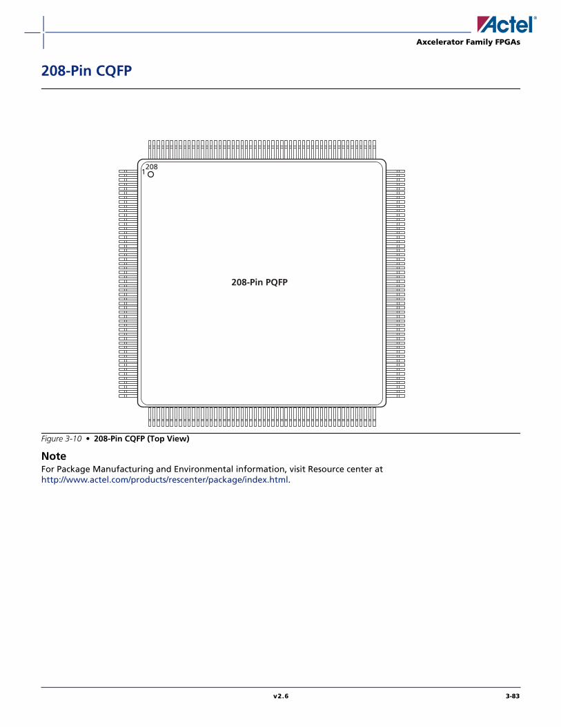
Axcelerator Family FPGAs
v2.6 3-83
208-Pin CQFP
NoteFor Package Manufacturing and Environmental information, visit Resource center athttp://www.actel.com/products/rescenter/package/index.html.
Figure 3-10 • 208-Pin CQFP (Top View)
208-Pin PQFP
1208

Axcelerator Family FPGAs
3-84 v2.6
208-Pin CQFP
AX250 Function Pin #
Bank 0
IO02NB0F0 197
IO03NB0F0 198
IO03PB0F0 199
IO12NB0F0/HCLKAN 191
IO12PB0F0/HCLKAP 192
IO13NB0F0/HCLKBN 185
IO13PB0F0/HCLKBP 186
Bank 1
IO14NB1F1/HCLKCN 180
IO14PB1F1/HCLKCP 181
IO15NB1F1/HCLKDN 174
IO15PB1F1/HCLKDP 175
IO16NB1F1 170
IO16PB1F1 171
IO24NB1F1 165
IO24PB1F1 166
IO26NB1F1 161
IO26PB1F1 162
IO27NB1F1 159
IO27PB1F1 160
Bank 2
IO29NB2F2 151
IO29PB2F2 153
IO30NB2F2 152
IO30PB2F2 154
IO31PB2F2 148
IO32NB2F2 146
IO32PB2F2 147
IO34NB2F2 144
IO34PB2F2 145
IO39NB2F2 139
IO39PB2F2 140
IO40PB2F2 141
IO41NB2F2 137
IO41PB2F2 138
IO43NB2F2 132
IO43PB2F2 134
IO44NB2F2 131
IO44PB2F2 133
Bank 3
IO45NB3F3 127
IO45PB3F3 129
IO46NB3F3 126
IO46PB3F3 128
IO48NB3F3 122
IO48PB3F3 123
IO50NB3F3 120
IO50PB3F3 121
IO55NB3F3 116
IO55PB3F3 117
IO57NB3F3 114
IO57PB3F3 115
IO59NB3F3 110
IO59PB3F3 111
IO60NB3F3 108
IO60PB3F3 109
IO61NB3F3 106
IO61PB3F3 107
Bank 4
IO62NB4F4 100
IO62PB4F4 103
IO63NB4F4 101
IO63PB4F4 102
IO64NB4F4 96
IO64PB4F4 97
IO72NB4F4 91
IO72PB4F4 92
IO74NB4F4/CLKEN 87
IO74PB4F4/CLKEP 88
IO75NB4F4/CLKFN 81
IO75PB4F4/CLKFP 82
Bank 5
IO76NB5F5/CLKGN 76
208-Pin CQFP
AX250 Function Pin #
IO76PB5F5/CLKGP 77
IO77NB5F5/CLKHN 70
IO77PB5F5/CLKHP 71
IO78NB5F5 66
IO78PB5F5 67
IO86NB5F5 62
IO87NB5F5 60
IO87PB5F5 61
IO88NB5F5 56
IO88PB5F5 57
IO89NB5F5 54
IO89PB5F5 55
Bank 6
IO91NB6F6 47
IO91PB6F6 49
IO92NB6F6 48
IO92PB6F6 50
IO93NB6F6 42
IO93PB6F6 43
IO94PB6F6 44
IO96NB6F6 40
IO96PB6F6 41
IO101NB6F6 35
IO101PB6F6 36
IO102PB6F6 37
IO103NB6F6 33
IO103PB6F6 34
IO105NB6F6 28
IO105PB6F6 30
IO106NB6F6 27
IO106PB6F6 29
Bank 7
IO107NB7F7 23
IO107PB7F7 25
IO108NB7F7 22
IO108PB7F7 24
IO110NB7F7 18
208-Pin CQFP
AX250 Function Pin #

Axcelerator Family FPGAs
v2.6 3-85
IO110PB7F7 19
IO112NB7F7 16
IO112PB7F7 17
IO117NB7F7 12
IO117PB7F7 13
IO119NB7F7 10
IO119PB7F7 11
IO121PB7F7 7
IO122NB7F7 5
IO122PB7F7 6
IO123NB7F7 3
IO123PB7F7 4
Dedicated I/O
GND 9
GND 15
GND 21
GND 32
GND 39
GND 46
GND 51
GND 59
GND 65
GND 69
GND 90
GND 94
GND 99
GND 104
GND 113
GND 119
GND 125
GND 136
GND 143
GND 150
GND 155
GND 164
GND 169
GND 173
208-Pin CQFP
AX250 Function Pin #
GND 194
GND 196
GND 201
GND/LP 208
PRA 184
PRB 183
PRC 80
PRD 79
TCK 205
TDI 204
TDO 203
TMS 206
TRST 207
VCCA 2
VCCA 14
VCCA 38
VCCA 52
VCCA 64
VCCA 93
VCCA 118
VCCA 142
VCCA 156
VCCA 168
VCCA 195
VCCDA 1
VCCDA 26
VCCDA 53
VCCDA 63
VCCDA 78
VCCDA 95
VCCDA 105
VCCDA 130
VCCDA 157
VCCDA 167
VCCDA 182
VCCDA 202
VCCIB0 193
208-Pin CQFP
AX250 Function Pin #
VCCIB0 200
VCCIB1 163
VCCIB1 172
VCCIB2 135
VCCIB2 149
VCCIB3 112
VCCIB3 124
VCCIB4 89
VCCIB4 98
VCCIB5 58
VCCIB5 68
VCCIB6 31
VCCIB6 45
VCCIB7 8
VCCIB7 20
VCCPLA 189
VCCPLB 187
VCCPLC 178
VCCPLD 176
VCCPLE 85
VCCPLF 83
VCCPLG 74
VCCPLH 72
VCOMPLA 190
VCOMPLB 188
VCOMPLC 179
VCOMPLD 177
VCOMPLE 86
VCOMPLF 84
VCOMPLG 75
VCOMPLH 73
VPUMP 158
208-Pin CQFP
AX250 Function Pin #

Axcelerator Family FPGAs
3-86 v2.6
208 CQFP
AX500 Function Pin #
Bank 0
IO03NB0F0 198
IO03PB0F0 199
IO04NB0F0 197
IO19NB0F1/HCLKAN 191
IO19PB0F1/HCLKAP 192
IO20NB0F1/HCLKBN 185
IO20PB0F1/HCLKBP 186
Bank 1
IO21NB1F2/HCLKCN 180
IO21PB1F2/HCLKCP 181
IO22NB1F2/HCLKDN 174
IO22PB1F2/HCLKDP 175
IO23NB1F2 170
IO23PB1F2 171
IO37NB1F3 165
IO37PB1F3 166
IO39NB1F3 161
IO39PB1F3 162
IO41NB1F3 159
IO41PB1F3 160
Bank 2
IO43NB2F4 151
IO43PB2F4 153
IO44NB2F4 152
IO44PB2F4 154
IO45PB2F4 148
IO46NB2F4 146
IO46PB2F4 147
IO48NB2F4 144
IO48PB2F4 145
IO57NB2F5 139
IO57PB2F5 140
IO58PB2F5 141
IO59NB2F5 137
IO59PB2F5 138
IO61NB2F5 132
IO61PB2F5 134
IO62NB2F5 131
IO62PB2F5 133
Bank 3
IO63NB3F6 127
IO63PB3F6 129
IO64NB3F6 126
IO64PB3F6 128
IO66NB3F6 122
IO66PB3F6 123
IO68NB3F6 120
IO68PB3F6 121
IO77NB3F7 116
IO77PB3F7 117
IO79NB3F7 114
IO79PB3F7 115
IO81NB3F7 110
IO81PB3F7 111
IO82NB3F7 108
IO82PB3F7 109
IO83NB3F7 106
IO83PB3F7 107
Bank 4
IO84PB4F8 103
IO85NB4F8 100
IO86NB4F8 101
IO86PB4F8 102
IO87NB4F8 96
IO87PB4F8 97
IO101NB4F9 91
IO101PB4F9 92
IO103NB4F9/CLKEN 87
IO103PB4F9/CLKEP 88
IO104NB4F9/CLKFN 81
IO104PB4F9/CLKFP 82
Bank 5
IO105NB5F10/CLKGN 76
208 CQFP
AX500 Function Pin #
IO105PB5F10/CLKGP 77
IO106NB5F10/CLKHN 70
IO106PB5F10/CLKHP 71
IO107NB5F10 66
IO107PB5F10 67
IO119NB5F11 62
IO121NB5F11 60
IO121PB5F11 61
IO123NB5F11 56
IO123PB5F11 57
IO125NB5F11 54
IO125PB5F11 55
Bank 6
IO127NB6F12 47
IO127PB6F12 49
IO128NB6F12 48
IO128PB6F12 50
IO129NB6F12 42
IO129PB6F12 43
IO130PB6F12 44
IO132NB6F12 40
IO132PB6F12 41
IO141NB6F13 35
IO141PB6F13 36
IO142PB6F13 37
IO143NB6F13 33
IO143PB6F13 34
IO145NB6F13 28
IO145PB6F13 30
IO146NB6F13 27
IO146PB6F13 29
Bank 7
IO147NB7F14 23
IO147PB7F14 25
IO148NB7F14 22
IO148PB7F14 24
IO150NB7F14 18
208 CQFP
AX500 Function Pin #
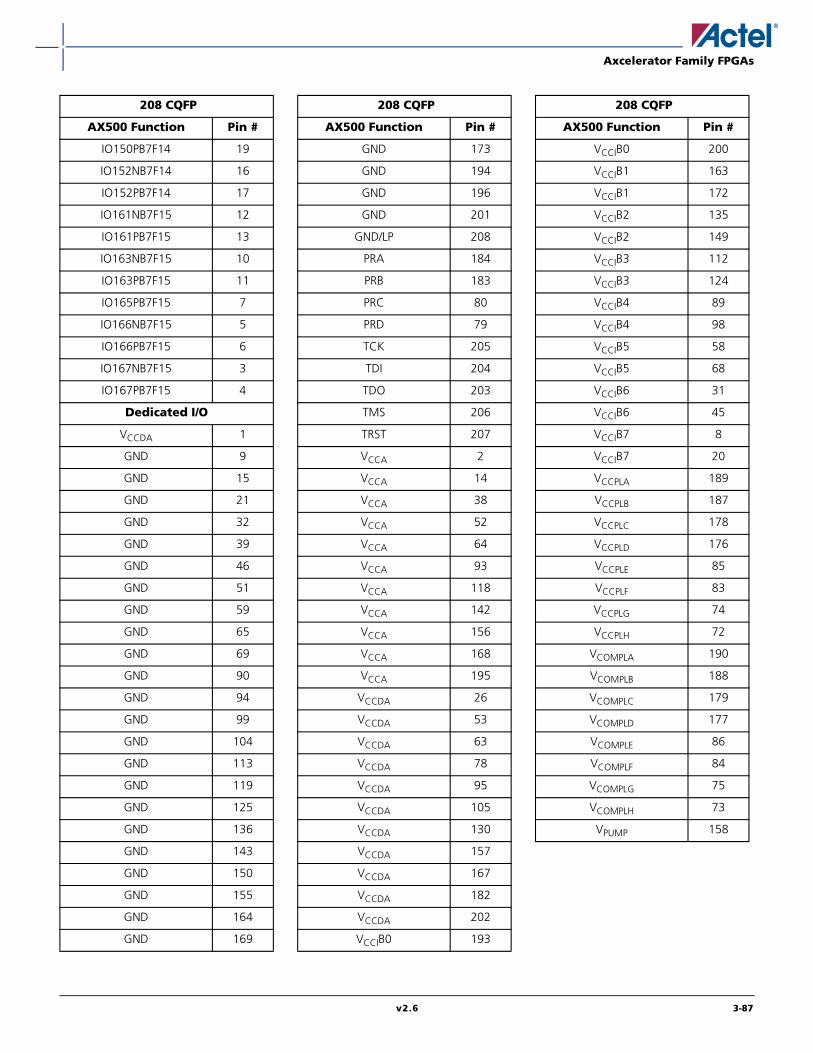
Axcelerator Family FPGAs
v2.6 3-87
IO150PB7F14 19
IO152NB7F14 16
IO152PB7F14 17
IO161NB7F15 12
IO161PB7F15 13
IO163NB7F15 10
IO163PB7F15 11
IO165PB7F15 7
IO166NB7F15 5
IO166PB7F15 6
IO167NB7F15 3
IO167PB7F15 4
Dedicated I/O
VCCDA 1
GND 9
GND 15
GND 21
GND 32
GND 39
GND 46
GND 51
GND 59
GND 65
GND 69
GND 90
GND 94
GND 99
GND 104
GND 113
GND 119
GND 125
GND 136
GND 143
GND 150
GND 155
GND 164
GND 169
208 CQFP
AX500 Function Pin #
GND 173
GND 194
GND 196
GND 201
GND/LP 208
PRA 184
PRB 183
PRC 80
PRD 79
TCK 205
TDI 204
TDO 203
TMS 206
TRST 207
VCCA 2
VCCA 14
VCCA 38
VCCA 52
VCCA 64
VCCA 93
VCCA 118
VCCA 142
VCCA 156
VCCA 168
VCCA 195
VCCDA 26
VCCDA 53
VCCDA 63
VCCDA 78
VCCDA 95
VCCDA 105
VCCDA 130
VCCDA 157
VCCDA 167
VCCDA 182
VCCDA 202
VCCIB0 193
208 CQFP
AX500 Function Pin #
VCCIB0 200
VCCIB1 163
VCCIB1 172
VCCIB2 135
VCCIB2 149
VCCIB3 112
VCCIB3 124
VCCIB4 89
VCCIB4 98
VCCIB5 58
VCCIB5 68
VCCIB6 31
VCCIB6 45
VCCIB7 8
VCCIB7 20
VCCPLA 189
VCCPLB 187
VCCPLC 178
VCCPLD 176
VCCPLE 85
VCCPLF 83
VCCPLG 74
VCCPLH 72
VCOMPLA 190
VCOMPLB 188
VCOMPLC 179
VCOMPLD 177
VCOMPLE 86
VCOMPLF 84
VCOMPLG 75
VCOMPLH 73
VPUMP 158
208 CQFP
AX500 Function Pin #

Axcelerator Family FPGAs
3-88 v2.6
352-Pin CQFP
NoteFor Package Manufacturing and Environmental information, visit Resource center athttp://www.actel.com/products/rescenter/package/index.html.
Figure 3-11 • 352-Pin CQFP (Top View)
CeramicTie Bar
Pin 1
352-Pin CQFP
1234
264263262261
414243444546474849
85868788
180179178177
223222221220219218217216215
352
351
350
349
339
338
337
336
335
334
333
332
331
268
267
266
265
89 90 91 92 127
128
129
130
131
132
133
134
135
173
174
175
176

Axcelerator Family FPGAs
v2.6 3-89
352-Pin CQFP
AX250 Function Pin #
Bank 0
IO00NB0F0 341
IO00PB0F0 342
IO01NB0F0 343
IO02NB0F0 337
IO02PB0F0 338
IO04NB0F0 335
IO04PB0F0 336
IO06NB0F0 331
IO06PB0F0 332
IO08NB0F0 325
IO08PB0F0 326
IO10NB0F0 323
IO10PB0F0 324
IO12NB0F0/HCLKAN 319
IO12PB0F0/HCLKAP 320
IO13NB0F0/HCLKBN 313
IO13PB0F0/HCLKBP 314
Bank 1
IO14NB1F1/HCLKCN 305
IO14PB1F1/HCLKCP 306
IO15NB1F1/HCLKDN 299
IO15PB1F1/HCLKDP 300
IO16NB1F1 289
IO16PB1F1 290
IO17NB1F1 295
IO17PB1F1 296
IO18NB1F1 287
IO18PB1F1 288
IO20NB1F1 283
IO20PB1F1 284
IO22NB1F1 277
IO22PB1F1 278
IO23NB1F1 281
IO23PB1F1 282
IO24NB1F1 275
IO24PB1F1 276
IO25NB1F1 271
IO25PB1F1 272
IO27NB1F1 269
IO27PB1F1 270
Bank 2
IO29NB2F2 261
IO29PB2F2 262
IO30NB2F2 259
IO30PB2F2 260
IO31NB2F2 255
IO31PB2F2 256
IO33NB2F2 249
IO33PB2F2 250
IO34NB2F2 253
IO34PB2F2 254
IO35NB2F2 247
IO35PB2F2 248
IO36NB2F2 243
IO36PB2F2 244
IO37NB2F2 241
IO37PB2F2 242
IO38NB2F2 237
IO38PB2F2 238
IO39NB2F2 235
IO39PB2F2 236
IO41NB2F2 231
IO41PB2F2 232
IO42NB2F2 229
IO42PB2F2 230
IO43NB2F2 225
IO43PB2F2 226
IO44NB2F2 223
IO44PB2F2 224
Bank 3
IO45NB3F3 217
IO45PB3F3 218
IO46NB3F3 219
352-Pin CQFP
AX250 Function Pin #
IO46PB3F3 220
IO47NB3F3 213
IO47PB3F3 214
IO48NB3F3 211
IO48PB3F3 212
IO49NB3F3 207
IO49PB3F3 208
IO51NB3F3 205
IO51PB3F3 206
IO52NB3F3 201
IO52PB3F3 202
IO53NB3F3 199
IO53PB3F3 200
IO54NB3F3 195
IO54PB3F3 196
IO55NB3F3 193
IO55PB3F3 194
IO56NB3F3 187
IO56PB3F3 188
IO57NB3F3 189
IO57PB3F3 190
IO59NB3F3 183
IO59PB3F3 184
IO60NB3F3 181
IO60PB3F3 182
IO61NB3F3 179
IO61PB3F3 180
Bank 4
IO62NB4F4 172
IO62PB4F4 173
IO64NB4F4 166
IO64PB4F4 167
IO65NB4F4 170
IO65PB4F4 171
IO66NB4F4 164
IO66PB4F4 165
IO67NB4F4 160
352-Pin CQFP
AX250 Function Pin #

Axcelerator Family FPGAs
3-90 v2.6
IO67PB4F4 161
IO68NB4F4 158
IO68PB4F4 159
IO70NB4F4 154
IO70PB4F4 155
IO72NB4F4 152
IO72PB4F4 153
IO73NB4F4 146
IO73PB4F4 147
IO74NB4F4/CLKEN 142
IO74PB4F4/CLKEP 143
IO75NB4F4/CLKFN 136
IO75PB4F4/CLKFP 137
Bank 5
IO76NB5F5/CLKGN 128
IO76PB5F5/CLKGP 129
IO77NB5F5/CLKHN 122
IO77PB5F5/CLKHP 123
IO78NB5F5 112
IO78PB5F5 113
IO79NB5F5 118
IO79PB5F5 119
IO80NB5F5 110
IO80PB5F5 111
IO82NB5F5 106
IO82PB5F5 107
IO84NB5F5 100
IO84PB5F5 101
IO85NB5F5 104
IO85PB5F5 105
IO86NB5F5 98
IO86PB5F5 99
IO87NB5F5 94
IO87PB5F5 95
IO89NB5F5 92
IO89PB5F5 93
Bank 6
352-Pin CQFP
AX250 Function Pin #
IO90PB6F6 86
IO91NB6F6 84
IO91PB6F6 85
IO92NB6F6 78
IO92PB6F6 79
IO93NB6F6 82
IO93PB6F6 83
IO95NB6F6 76
IO95PB6F6 77
IO96NB6F6 72
IO96PB6F6 73
IO97NB6F6 70
IO97PB6F6 71
IO98NB6F6 66
IO98PB6F6 67
IO99NB6F6 64
IO99PB6F6 65
IO100NB6F6 60
IO100PB6F6 61
IO101NB6F6 58
IO101PB6F6 59
IO103NB6F6 54
IO103PB6F6 55
IO104NB6F6 52
IO104PB6F6 53
IO105NB6F6 48
IO105PB6F6 49
IO106NB6F6 46
IO106PB6F6 47
Bank 7
IO107NB7F7 40
IO107PB7F7 41
IO108NB7F7 42
IO108PB7F7 43
IO109NB7F7 36
IO109PB7F7 37
IO110NB7F7 34
352-Pin CQFP
AX250 Function Pin #
IO110PB7F7 35
IO111NB7F7 30
IO111PB7F7 31
IO113NB7F7 28
IO113PB7F7 29
IO114NB7F7 24
IO114PB7F7 25
IO115NB7F7 22
IO115PB7F7 23
IO116NB7F7 18
IO116PB7F7 19
IO117NB7F7 16
IO117PB7F7 17
IO118NB7F7 12
IO118PB7F7 13
IO119NB7F7 10
IO119PB7F7 11
IO121NB7F7 6
IO121PB7F7 7
IO123NB7F7 4
IO123PB7F7 5
Dedicated I/O
GND 1
GND 9
GND 15
GND 21
GND 27
GND 33
GND 39
GND 45
GND 51
GND 57
GND 63
GND 69
GND 75
GND 81
GND 88
352-Pin CQFP
AX250 Function Pin #
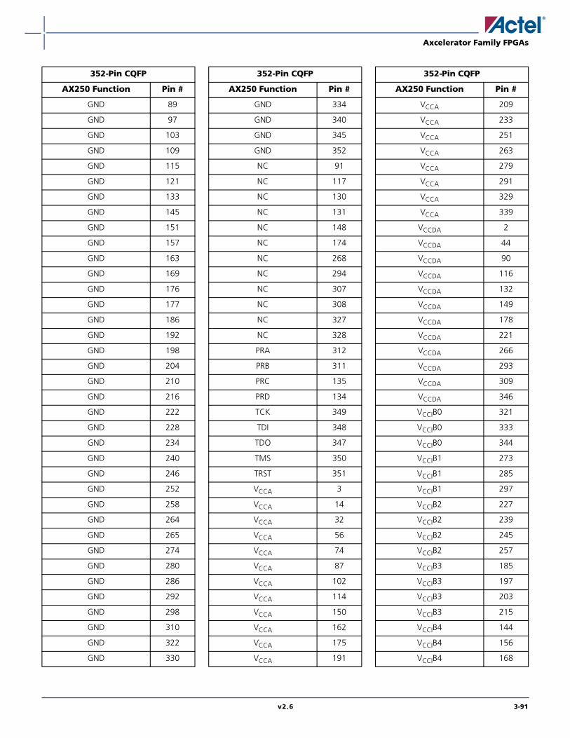
Axcelerator Family FPGAs
v2.6 3-91
GND 89
GND 97
GND 103
GND 109
GND 115
GND 121
GND 133
GND 145
GND 151
GND 157
GND 163
GND 169
GND 176
GND 177
GND 186
GND 192
GND 198
GND 204
GND 210
GND 216
GND 222
GND 228
GND 234
GND 240
GND 246
GND 252
GND 258
GND 264
GND 265
GND 274
GND 280
GND 286
GND 292
GND 298
GND 310
GND 322
GND 330
352-Pin CQFP
AX250 Function Pin #
GND 334
GND 340
GND 345
GND 352
NC 91
NC 117
NC 130
NC 131
NC 148
NC 174
NC 268
NC 294
NC 307
NC 308
NC 327
NC 328
PRA 312
PRB 311
PRC 135
PRD 134
TCK 349
TDI 348
TDO 347
TMS 350
TRST 351
VCCA 3
VCCA 14
VCCA 32
VCCA 56
VCCA 74
VCCA 87
VCCA 102
VCCA 114
VCCA 150
VCCA 162
VCCA 175
VCCA 191
352-Pin CQFP
AX250 Function Pin #
VCCA 209
VCCA 233
VCCA 251
VCCA 263
VCCA 279
VCCA 291
VCCA 329
VCCA 339
VCCDA 2
VCCDA 44
VCCDA 90
VCCDA 116
VCCDA 132
VCCDA 149
VCCDA 178
VCCDA 221
VCCDA 266
VCCDA 293
VCCDA 309
VCCDA 346
VCCIB0 321
VCCIB0 333
VCCIB0 344
VCCIB1 273
VCCIB1 285
VCCIB1 297
VCCIB2 227
VCCIB2 239
VCCIB2 245
VCCIB2 257
VCCIB3 185
VCCIB3 197
VCCIB3 203
VCCIB3 215
VCCIB4 144
VCCIB4 156
VCCIB4 168
352-Pin CQFP
AX250 Function Pin #

Axcelerator Family FPGAs
3-92 v2.6
VCCIB5 96
VCCIB5 108
VCCIB5 120
VCCIB6 50
VCCIB6 62
VCCIB6 68
VCCIB6 80
VCCIB7 8
VCCIB7 20
VCCIB7 26
VCCIB7 38
VCCPLA 317
VCCPLB 315
VCCPLC 303
VCCPLD 301
VCCPLE 140
VCCPLF 138
VCCPLG 126
VCCPLH 124
VCOMPLA 318
VCOMPLB 316
VCOMPLC 304
VCOMPLD 302
VCOMPLE 141
VCOMPLF 139
VCOMPLG 127
VCOMPLH 125
VPUMP 267
352-Pin CQFP
AX250 Function Pin #
352-Pin CQFP
AX500 Function Pin #
Bank 0
IO00PB0F0 343
IO03NB0F0 341
IO03PB0F0 342
IO05NB0F0 337
IO05PB0F0 338
IO07NB0F0 335
IO07PB0F0 336
IO09NB0F0 331
IO09PB0F0 332
IO15NB0F1 325
IO15PB0F1 326
IO17NB0F1 323
IO17PB0F1 324
IO19NB0F1/HCLKAN 319
IO19PB0F1/HCLKAP 320
IO20NB0F1/HCLKBN 313
IO20PB0F1/HCLKBP 314
Bank 1
IO21NB1F2/HCLKCN 305
IO21PB1F2/HCLKCP 306
IO22NB1F2/HCLKDN 299
IO22PB1F2/HCLKDP 300
IO23NB1F2 289
IO23PB1F2 290
IO24NB1F2 295
IO24PB1F2 296
IO25NB1F2 287
IO25PB1F2 288
IO27NB1F2 283
IO27PB1F2 284
IO29NB1F2 281
IO29PB1F2 282
IO31NB1F2 277
IO31PB1F2 278
IO35NB1F3 275
IO35PB1F3 276
IO37NB1F3 271
IO37PB1F3 272
IO41NB1F3 269
IO41PB1F3 270
Bank 2
IO43NB2F4 261
IO43PB2F4 262
IO45NB2F4 259
IO45PB2F4 260
IO47NB2F4 255
IO47PB2F4 256
IO49NB2F4 253
IO49PB2F4 254
IO50NB2F4 247
IO50PB2F4 248
IO51NB2F4 249
IO51PB2F4 250
IO53NB2F5 243
IO53PB2F5 244
IO54NB2F5 241
IO54PB2F5 242
IO55NB2F5 237
IO55PB2F5 238
IO57NB2F5 235
IO57PB2F5 236
IO58NB2F5 231
IO58PB2F5 232
IO59NB2F5 229
IO59PB2F5 230
IO61NB2F5 225
IO61PB2F5 226
IO62NB2F5 223
IO62PB2F5 224
Bank 3
IO63NB3F6 217
IO63PB3F6 218
IO64NB3F6 219
352-Pin CQFP
AX500 Function Pin #
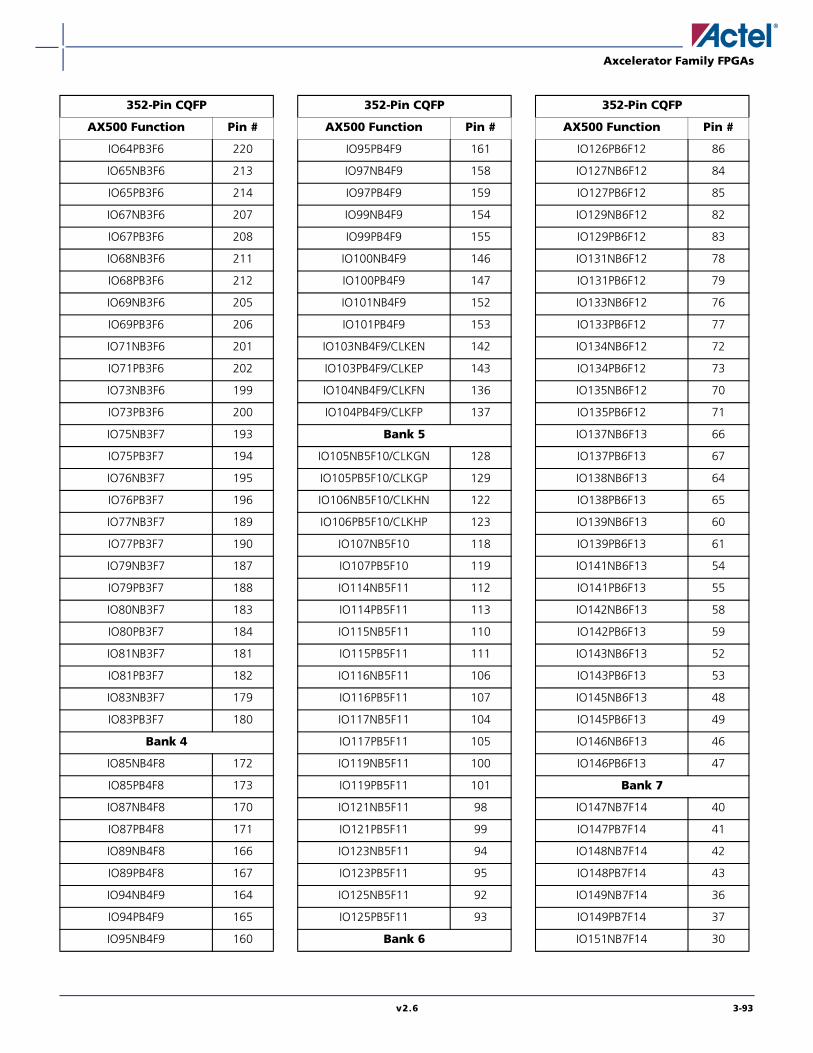
Axcelerator Family FPGAs
v2.6 3-93
IO64PB3F6 220
IO65NB3F6 213
IO65PB3F6 214
IO67NB3F6 207
IO67PB3F6 208
IO68NB3F6 211
IO68PB3F6 212
IO69NB3F6 205
IO69PB3F6 206
IO71NB3F6 201
IO71PB3F6 202
IO73NB3F6 199
IO73PB3F6 200
IO75NB3F7 193
IO75PB3F7 194
IO76NB3F7 195
IO76PB3F7 196
IO77NB3F7 189
IO77PB3F7 190
IO79NB3F7 187
IO79PB3F7 188
IO80NB3F7 183
IO80PB3F7 184
IO81NB3F7 181
IO81PB3F7 182
IO83NB3F7 179
IO83PB3F7 180
Bank 4
IO85NB4F8 172
IO85PB4F8 173
IO87NB4F8 170
IO87PB4F8 171
IO89NB4F8 166
IO89PB4F8 167
IO94NB4F9 164
IO94PB4F9 165
IO95NB4F9 160
352-Pin CQFP
AX500 Function Pin #
IO95PB4F9 161
IO97NB4F9 158
IO97PB4F9 159
IO99NB4F9 154
IO99PB4F9 155
IO100NB4F9 146
IO100PB4F9 147
IO101NB4F9 152
IO101PB4F9 153
IO103NB4F9/CLKEN 142
IO103PB4F9/CLKEP 143
IO104NB4F9/CLKFN 136
IO104PB4F9/CLKFP 137
Bank 5
IO105NB5F10/CLKGN 128
IO105PB5F10/CLKGP 129
IO106NB5F10/CLKHN 122
IO106PB5F10/CLKHP 123
IO107NB5F10 118
IO107PB5F10 119
IO114NB5F11 112
IO114PB5F11 113
IO115NB5F11 110
IO115PB5F11 111
IO116NB5F11 106
IO116PB5F11 107
IO117NB5F11 104
IO117PB5F11 105
IO119NB5F11 100
IO119PB5F11 101
IO121NB5F11 98
IO121PB5F11 99
IO123NB5F11 94
IO123PB5F11 95
IO125NB5F11 92
IO125PB5F11 93
Bank 6
352-Pin CQFP
AX500 Function Pin #
IO126PB6F12 86
IO127NB6F12 84
IO127PB6F12 85
IO129NB6F12 82
IO129PB6F12 83
IO131NB6F12 78
IO131PB6F12 79
IO133NB6F12 76
IO133PB6F12 77
IO134NB6F12 72
IO134PB6F12 73
IO135NB6F12 70
IO135PB6F12 71
IO137NB6F13 66
IO137PB6F13 67
IO138NB6F13 64
IO138PB6F13 65
IO139NB6F13 60
IO139PB6F13 61
IO141NB6F13 54
IO141PB6F13 55
IO142NB6F13 58
IO142PB6F13 59
IO143NB6F13 52
IO143PB6F13 53
IO145NB6F13 48
IO145PB6F13 49
IO146NB6F13 46
IO146PB6F13 47
Bank 7
IO147NB7F14 40
IO147PB7F14 41
IO148NB7F14 42
IO148PB7F14 43
IO149NB7F14 36
IO149PB7F14 37
IO151NB7F14 30
352-Pin CQFP
AX500 Function Pin #
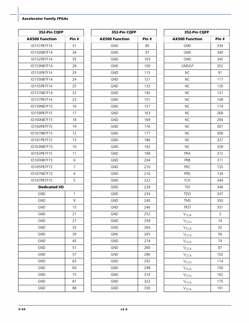
Axcelerator Family FPGAs
3-94 v2.6
IO151PB7F14 31
IO152NB7F14 34
IO152PB7F14 35
IO153NB7F14 28
IO153PB7F14 29
IO155NB7F14 24
IO155PB7F14 25
IO157NB7F14 22
IO157PB7F14 23
IO159NB7F15 16
IO159PB7F15 17
IO160NB7F15 18
IO160PB7F15 19
IO161NB7F15 12
IO161PB7F15 13
IO163NB7F15 10
IO163PB7F15 11
IO165NB7F15 6
IO165PB7F15 7
IO167NB7F15 4
IO167PB7F15 5
Dedicated I/O
GND 1
GND 9
GND 15
GND 21
GND 27
GND 33
GND 39
GND 45
GND 51
GND 57
GND 63
GND 69
GND 75
GND 81
GND 88
352-Pin CQFP
AX500 Function Pin #
GND 89
GND 97
GND 103
GND 109
GND 115
GND 121
GND 133
GND 145
GND 151
GND 157
GND 163
GND 169
GND 176
GND 177
GND 186
GND 192
GND 198
GND 204
GND 210
GND 216
GND 222
GND 228
GND 234
GND 240
GND 246
GND 252
GND 258
GND 264
GND 265
GND 274
GND 280
GND 286
GND 292
GND 298
GND 310
GND 322
GND 330
352-Pin CQFP
AX500 Function Pin #
GND 334
GND 340
GND 345
GND/LP 352
NC 91
NC 117
NC 130
NC 131
NC 148
NC 174
NC 268
NC 294
NC 307
NC 308
NC 327
NC 328
PRA 312
PRB 311
PRC 135
PRD 134
TCK 349
TDI 348
TDO 347
TMS 350
TRST 351
VCCA 3
VCCA 14
VCCA 32
VCCA 56
VCCA 74
VCCA 87
VCCA 102
VCCA 114
VCCA 150
VCCA 162
VCCA 175
VCCA 191
352-Pin CQFP
AX500 Function Pin #

Axcelerator Family FPGAs
v2.6 3-95
VCCA 209
VCCA 233
VCCA 251
VCCA 263
VCCA 279
VCCA 291
VCCA 329
VCCA 339
VCCDA 2
VCCDA 44
VCCDA 90
VCCDA 116
VCCDA 132
VCCDA 149
VCCDA 178
VCCDA 221
VCCDA 266
VCCDA 293
VCCDA 309
VCCDA 346
VCCIB0 321
VCCIB0 333
VCCIB0 344
VCCIB1 273
VCCIB1 285
VCCIB1 297
VCCIB2 227
VCCIB2 239
VCCIB2 245
VCCIB2 257
VCCIB3 185
VCCIB3 197
VCCIB3 203
VCCIB3 215
VCCIB4 144
VCCIB4 156
VCCIB4 168
352-Pin CQFP
AX500 Function Pin #
VCCIB5 96
VCCIB5 108
VCCIB5 120
VCCIB6 50
VCCIB6 62
VCCIB6 68
VCCIB6 80
VCCIB7 8
VCCIB7 20
VCCIB7 26
VCCIB7 38
VCCPLA 317
VCCPLB 315
VCCPLC 303
VCCPLD 301
VCCPLE 140
VCCPLF 138
VCCPLG 126
VCCPLH 124
VCOMPLA 318
VCOMPLB 316
VCOMPLC 304
VCOMPLD 302
VCOMPLE 141
VCOMPLF 139
VCOMPLG 127
VCOMPLH 125
VPUMP 267
352-Pin CQFP
AX500 Function Pin #
352-Pin CQFP
AX1000 Function Pin #
Bank 0
IO02NB0F0 341
IO02PB0F0 342
IO03PB0F0 343
IO04NB0F0 337
IO04PB0F0 338
IO08NB0F0 331
IO08PB0F0 332
IO09NB0F0 335
IO09PB0F0 336
IO24NB0F2 325
IO24PB0F2 326
IO25NB0F2 323
IO25PB0F2 324
IO30NB0F2/HCLKAN 319
IO30PB0F2/HCLKAP 320
IO31NB0F2/HCLKBN 313
IO31PB0F2/HCLKBP 314
Bank 1
IO32NB1F3/HCLKCN 305
IO32PB1F3/HCLKCP 306
IO33NB1F3/HCLKDN 299
IO33PB1F3/HCLKDP 300
IO38NB1F3 295
IO38PB1F3 296
IO54NB1F5 287
IO54PB1F5 288
IO55NB1F5 289
IO55PB1F5 290
IO56NB1F5 281
IO56PB1F5 282
IO57NB1F5 283
IO57PB1F5 284
IO59NB1F5 277
IO59PB1F5 278
IO60NB1F5 275
IO60PB1F5 276
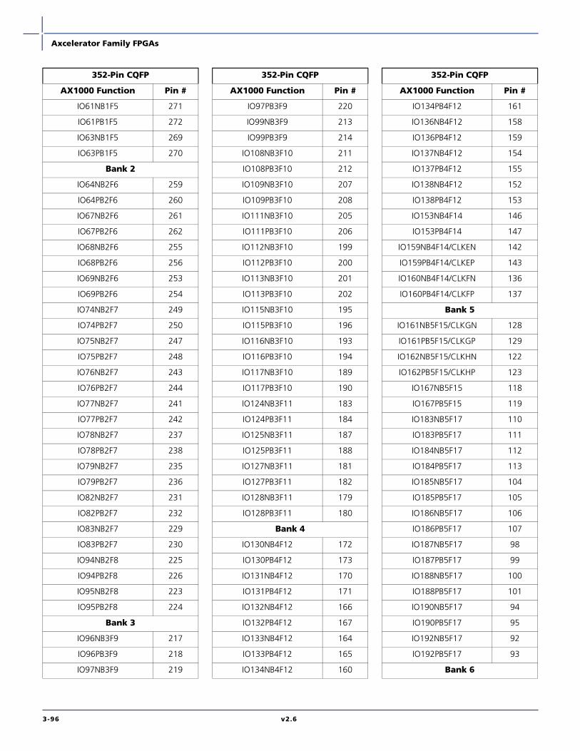
Axcelerator Family FPGAs
3-96 v2.6
IO61NB1F5 271
IO61PB1F5 272
IO63NB1F5 269
IO63PB1F5 270
Bank 2
IO64NB2F6 259
IO64PB2F6 260
IO67NB2F6 261
IO67PB2F6 262
IO68NB2F6 255
IO68PB2F6 256
IO69NB2F6 253
IO69PB2F6 254
IO74NB2F7 249
IO74PB2F7 250
IO75NB2F7 247
IO75PB2F7 248
IO76NB2F7 243
IO76PB2F7 244
IO77NB2F7 241
IO77PB2F7 242
IO78NB2F7 237
IO78PB2F7 238
IO79NB2F7 235
IO79PB2F7 236
IO82NB2F7 231
IO82PB2F7 232
IO83NB2F7 229
IO83PB2F7 230
IO94NB2F8 225
IO94PB2F8 226
IO95NB2F8 223
IO95PB2F8 224
Bank 3
IO96NB3F9 217
IO96PB3F9 218
IO97NB3F9 219
352-Pin CQFP
AX1000 Function Pin #
IO97PB3F9 220
IO99NB3F9 213
IO99PB3F9 214
IO108NB3F10 211
IO108PB3F10 212
IO109NB3F10 207
IO109PB3F10 208
IO111NB3F10 205
IO111PB3F10 206
IO112NB3F10 199
IO112PB3F10 200
IO113NB3F10 201
IO113PB3F10 202
IO115NB3F10 195
IO115PB3F10 196
IO116NB3F10 193
IO116PB3F10 194
IO117NB3F10 189
IO117PB3F10 190
IO124NB3F11 183
IO124PB3F11 184
IO125NB3F11 187
IO125PB3F11 188
IO127NB3F11 181
IO127PB3F11 182
IO128NB3F11 179
IO128PB3F11 180
Bank 4
IO130NB4F12 172
IO130PB4F12 173
IO131NB4F12 170
IO131PB4F12 171
IO132NB4F12 166
IO132PB4F12 167
IO133NB4F12 164
IO133PB4F12 165
IO134NB4F12 160
352-Pin CQFP
AX1000 Function Pin #
IO134PB4F12 161
IO136NB4F12 158
IO136PB4F12 159
IO137NB4F12 154
IO137PB4F12 155
IO138NB4F12 152
IO138PB4F12 153
IO153NB4F14 146
IO153PB4F14 147
IO159NB4F14/CLKEN 142
IO159PB4F14/CLKEP 143
IO160NB4F14/CLKFN 136
IO160PB4F14/CLKFP 137
Bank 5
IO161NB5F15/CLKGN 128
IO161PB5F15/CLKGP 129
IO162NB5F15/CLKHN 122
IO162PB5F15/CLKHP 123
IO167NB5F15 118
IO167PB5F15 119
IO183NB5F17 110
IO183PB5F17 111
IO184NB5F17 112
IO184PB5F17 113
IO185NB5F17 104
IO185PB5F17 105
IO186NB5F17 106
IO186PB5F17 107
IO187NB5F17 98
IO187PB5F17 99
IO188NB5F17 100
IO188PB5F17 101
IO190NB5F17 94
IO190PB5F17 95
IO192NB5F17 92
IO192PB5F17 93
Bank 6
352-Pin CQFP
AX1000 Function Pin #

Axcelerator Family FPGAs
v2.6 3-97
IO193PB6F18 86
IO194NB6F18 84
IO194PB6F18 85
IO196NB6F18 78
IO196PB6F18 79
IO197NB6F18 82
IO197PB6F18 83
IO198NB6F18 76
IO198PB6F18 77
IO203NB6F19 72
IO203PB6F19 73
IO204NB6F19 70
IO204PB6F19 71
IO205NB6F19 66
IO205PB6F19 67
IO206NB6F19 64
IO206PB6F19 65
IO207NB6F19 60
IO207PB6F19 61
IO208NB6F19 58
IO208PB6F19 59
IO211NB6F19 54
IO211PB6F19 55
IO212NB6F19 52
IO212PB6F19 53
IO223NB6F20 48
IO223PB6F20 49
IO224NB6F20 46
IO224PB6F20 47
Bank 7
IO225NB7F21 40
IO225PB7F21 41
IO226NB7F21 42
IO226PB7F21 43
IO237NB7F22 34
IO237PB7F22 35
IO238NB7F22 36
352-Pin CQFP
AX1000 Function Pin #
IO238PB7F22 37
IO240NB7F22 30
IO240PB7F22 31
IO241NB7F22 28
IO241PB7F22 29
IO242NB7F22 24
IO242PB7F22 25
IO244NB7F22 22
IO244PB7F22 23
IO245NB7F22 18
IO245PB7F22 19
IO246NB7F22 16
IO246PB7F22 17
IO249NB7F23 12
IO249PB7F23 13
IO250NB7F23 10
IO250PB7F23 11
IO256NB7F23 4
IO256PB7F23 5
IO257NB7F23 6
IO257PB7F23 7
Dedicated I/O
GND 1
GND 9
GND 15
GND 21
GND 27
GND 33
GND 39
GND 45
GND 51
GND 57
GND 63
GND 69
GND 75
GND 81
GND 88
352-Pin CQFP
AX1000 Function Pin #
GND 89
GND 97
GND 103
GND 109
GND 115
GND 121
GND 133
GND 145
GND 151
GND 157
GND 163
GND 169
GND 176
GND 177
GND 186
GND 192
GND 198
GND 204
GND 210
GND 216
GND 222
GND 228
GND 234
GND 240
GND 246
GND 252
GND 258
GND 264
GND 265
GND 274
GND 280
GND 286
GND 292
GND 298
GND 310
GND 322
GND 330
352-Pin CQFP
AX1000 Function Pin #

Axcelerator Family FPGAs
3-98 v2.6
GND 334
GND 340
GND 345
GND 352
NC 91
NC 130
NC 131
NC 174
NC 268
NC 307
NC 308
PRA 312
PRB 311
PRC 135
PRD 134
TCK 349
TDI 348
TDO 347
TMS 350
TRST 351
VCCA 3
VCCA 14
VCCA 32
VCCA 56
VCCA 74
VCCA 87
VCCA 102
VCCA 114
VCCA 150
VCCA 162
VCCA 175
VCCA 191
VCCA 209
VCCA 233
VCCA 251
VCCA 263
VCCA 279
352-Pin CQFP
AX1000 Function Pin #
VCCA 291
VCCA 329
VCCA 339
VCCDA 2
VCCDA 44
VCCDA 90
VCCDA 116
VCCDA 117
VCCDA 132
VCCDA 148
VCCDA 149
VCCDA 178
VCCDA 221
VCCDA 266
VCCDA 293
VCCDA 294
VCCDA 309
VCCDA 327
VCCDA 328
VCCDA 346
VCCIB0 321
VCCIB0 333
VCCIB0 344
VCCIB1 273
VCCIB1 285
VCCIB1 297
VCCIB2 227
VCCIB2 239
VCCIB2 245
VCCIB2 257
VCCIB3 185
VCCIB3 197
VCCIB3 203
VCCIB3 215
VCCIB4 144
VCCIB4 156
VCCIB4 168
352-Pin CQFP
AX1000 Function Pin #
VCCIB5 96
VCCIB5 108
VCCIB5 120
VCCIB6 50
VCCIB6 62
VCCIB6 68
VCCIB6 80
VCCIB7 8
VCCIB7 20
VCCIB7 26
VCCIB7 38
VCCPLA 317
VCCPLB 315
VCCPLC 303
VCCPLD 301
VCCPLE 140
VCCPLF 138
VCCPLG 126
VCCPLH 124
VCOMPLA 318
VCOMPLB 316
VCOMPLC 304
VCOMPLD 302
VCOMPLE 141
VCOMPLF 139
VCOMPLG 127
VCOMPLH 125
VPUMP 267
352-Pin CQFP
AX1000 Function Pin #

Axcelerator Family FPGAs
v2.6 3-99
352-Pin CQFP
AX2000 Function Pin Number
Bank 0
IO01NB0F0 341
IO01PB0F0 342
IO02PB0F0 343
IO04NB0F0 337
IO04PB0F0 338
IO05NB0F0 335
IO05PB0F0 336
IO08NB0F0 331
IO08PB0F0 332
IO37NB0F3 325
IO37PB0F3 326
IO38NB0F3 323
IO38PB0F3 324
IO41NB0F3/HCLKAN 319
IO41PB0F3/HCLKAP 320
IO42NB0F3/HCLKBN 313
IO42PB0F3/HCLKBP 314
Bank 1
IO43NB1F4/HCLKCN 305
IO43PB1F4/HCLKCP 306
IO44NB1F4/HCLKDN 299
IO44PB1F4/HCLKDP 300
IO48NB1F4 295
IO48PB1F4 296
IO65NB1F6 283
IO65PB1F6 284
IO66NB1F6 289
IO66PB1F6 290
IO68NB1F6 287
IO68PB1F6 288
IO69NB1F6 275
IO69PB1F6 276
IO70NB1F6 281
IO70PB1F6 282
IO71NB1F6 277
IO71PB1F6 278
IO73NB1F6 269
IO73PB1F6 270
IO74NB1F6 271
IO74PB1F6 272
Bank 2
IO87NB2F8 261
IO87PB2F8 262
IO88NB2F8 255
IO88PB2F8 256
IO89NB2F8 259
IO89PB2F8 260
IO91NB2F8 253
IO91PB2F8 254
IO99NB2F9 249
IO99PB2F9 250
IO100NB2F9 247
IO100PB2F9 248
IO107NB2F10 243
IO107PB2F10 244
IO110NB2F10 241
IO110PB2F10 242
IO111NB2F10 237
IO111PB2F10 238
IO112NB2F10 235
IO112PB2F10 236
IO113NB2F10 231
IO113PB2F10 232
IO114NB2F10 229
IO114PB2F10 230
IO115NB2F10 225
IO115PB2F10 226
IO117NB2F10 223
IO117PB2F10 224
Bank 3
IO129NB3F12 219
IO129PB3F12 220
IO132NB3F12 217
IO132PB3F12 218
IO137NB3F12 213
IO137PB3F12 214
IO139NB3F13 211
IO139PB3F13 212
IO141NB3F13 205
IO141PB3F13 206
IO142NB3F13 207
352-Pin CQFP
AX2000 Function Pin Number
IO142PB3F13 208
IO145NB3F13 199
IO145PB3F13 200
IO146NB3F13 201
IO146PB3F13 202
IO147NB3F13 193
IO147PB3F13 194
IO148NB3F13 195
IO148PB3F13 196
IO149NB3F13 189
IO149PB3F13 190
IO161NB3F15 183
IO161PB3F15 184
IO163NB3F15 187
IO163PB3F15 188
IO165NB3F15 181
IO165PB3F15 182
IO167NB3F15 179
IO167PB3F15 180
Bank 4
IO181NB4F17 172
IO181PB4F17 173
IO182NB4F17 170
IO182PB4F17 171
IO183NB4F17 166
IO183PB4F17 167
IO184NB4F17 164
IO184PB4F17 165
IO185NB4F17 160
IO185PB4F17 161
IO190NB4F17 158
IO190PB4F17 159
IO191NB4F17 154
IO191PB4F17 155
IO192NB4F17 152
IO192PB4F17 153
IO207NB4F19 146
IO207PB4F19 147
IO212NB4F19/CLKEN 142
IO212PB4F19/CLKEP 143
IO213NB4F19/CLKFN 136
352-Pin CQFP
AX2000 Function Pin Number

Axcelerator Family FPGAs
3-100 v2.6
IO213PB4F19/CLKFP 137
Bank 5
IO214NB5F20/CLKGN 128
IO214PB5F20/CLKGP 129
IO215NB5F20/CLKHN 122
IO215PB5F20/CLKHP 123
IO217NB5F20 118
IO217PB5F20 119
IO236NB5F22 110
IO236PB5F22 111
IO237NB5F22 112
IO237PB5F22 113
IO238NB5F22 104
IO238PB5F22 105
IO239NB5F22 106
IO239PB5F22 107
IO240NB5F22 100
IO240PB5F22 101
IO242NB5F22 94
IO242PB5F22 95
IO243NB5F22 98
IO243PB5F22 99
IO244NB5F22 92
IO244PB5F22 93
Bank 6
IO257PB6F24 86
IO258NB6F24 84
IO258PB6F24 85
IO261NB6F24 82
IO261PB6F24 83
IO262NB6F24 78
IO262PB6F24 79
IO265NB6F24 76
IO265PB6F24 77
IO279NB6F26 72
IO279PB6F26 73
IO280NB6F26 70
IO280PB6F26 71
IO281NB6F26 66
IO281PB6F26 67
IO282NB6F26 64
352-Pin CQFP
AX2000 Function Pin Number
IO282PB6F26 65
IO284NB6F26 60
IO284PB6F26 61
IO285NB6F26 58
IO285PB6F26 59
IO286NB6F26 54
IO286PB6F26 55
IO287NB6F26 52
IO287PB6F26 53
IO294NB6F27 48
IO294PB6F27 49
IO296NB6F27 46
IO296PB6F27 47
Bank 7
IO300NB7F28 42
IO300PB7F28 43
IO303NB7F28 40
IO303PB7F28 41
IO310NB7F29 34
IO310PB7F29 35
IO311NB7F29 36
IO311PB7F29 37
IO312NB7F29 28
IO312PB7F29 29
IO315NB7F29 30
IO315PB7F29 31
IO316NB7F29 22
IO316PB7F29 23
IO317NB7F29 24
IO317PB7F29 25
IO318NB7F29 18
IO318PB7F29 19
IO320NB7F29 16
IO320PB7F29 17
IO334NB7F31 10
IO334PB7F31 11
IO335NB7F31 12
IO335PB7F31 13
IO338NB7F31 6
IO338PB7F31 7
IO341NB7F31 4
352-Pin CQFP
AX2000 Function Pin Number
IO341PB7F31 5
Dedicated I/O
GND 1
GND 9
GND 15
GND 21
GND 27
GND 33
GND 39
GND 45
GND 51
GND 57
GND 63
GND 69
GND 75
GND 81
GND 88
GND 89
GND 97
GND 103
GND 109
GND 115
GND 121
GND 133
GND 145
GND 151
GND 157
GND 163
GND 169
GND 176
GND 177
GND 186
GND 192
GND 198
GND 204
GND 210
GND 216
GND 222
GND 228
GND 234
GND 240
352-Pin CQFP
AX2000 Function Pin Number

Axcelerator Family FPGAs
v2.6 3-101
GND 246
GND 252
GND 258
GND 264
GND 265
GND 274
GND 280
GND 286
GND 292
GND 298
GND 310
GND 322
GND 330
GND 334
GND 340
GND 345
GND 352
PRA 312
PRB 311
PRC 135
PRD 134
TCK 349
TDI 348
TDO 347
TMS 350
TRST 351
VCCA 3
VCCA 14
VCCA 32
VCCA 56
VCCA 74
VCCA 87
VCCA 102
VCCA 114
VCCA 150
VCCA 162
VCCA 175
VCCA 191
VCCA 209
VCCA 233
VCCA 251
352-Pin CQFP
AX2000 Function Pin Number
VCCA 263
VCCA 279
VCCA 291
VCCA 329
VCCA 339
VCCDA 2
VCCDA 44
VCCDA 90
VCCDA 91
VCCDA 116
VCCDA 117
VCCDA 130
VCCDA 131
VCCDA 132
VCCDA 148
VCCDA 149
VCCDA 174
VCCDA 178
VCCDA 221
VCCDA 266
VCCDA 268
VCCDA 293
VCCDA 294
VCCDA 307
VCCDA 308
VCCDA 309
VCCDA 327
VCCDA 328
VCCDA 346
VCCIB0 321
VCCIB0 333
VCCIB0 344
VCCIB1 273
VCCIB1 285
VCCIB1 297
VCCIB2 227
VCCIB2 239
VCCIB2 245
VCCIB2 257
VCCIB3 185
VCCIB3 197
352-Pin CQFP
AX2000 Function Pin Number
VCCIB3 203
VCCIB3 215
VCCIB4 144
VCCIB4 156
VCCIB4 168
VCCIB5 96
VCCIB5 108
VCCIB5 120
VCCIB6 50
VCCIB6 62
VCCIB6 68
VCCIB6 80
VCCIB7 8
VCCIB7 20
VCCIB7 26
VCCIB7 38
VCCPLA 317
VCCPLB 315
VCCPLC 303
VCCPLD 301
VCCPLE 140
VCCPLF 138
VCCPLG 126
VCCPLH 124
VCOMPLA 318
VCOMPLB 316
VCOMPLC 304
VCOMPLD 302
VCOMPLE 141
VCOMPLF 139
VCOMPLG 127
VCOMPLH 125
VPUMP 267
352-Pin CQFP
AX2000 Function Pin Number

Axcelerator Family FPGAs
3-102 v2.6
624-Pin CCGA
NoteFor Package Manufacturing and Environmental information, visit Resource center athttp://www.actel.com/products/rescenter/package/index.html.
Figure 3-12 • 624-Pin CCGA (Bottom View)
1
A
B
C
D
E
F
G
H
JK
LM
N
P
R
T
U
VW
Y
AA
AB
AC
AD
AE
2345678910111214 131516171819202122232425

Axcelerator Family FPGAs
v2.6 3-103
624-Pin CCGA
AX1000 Function Pin Number
Bank 0
IO00NB0F0 F8
IO00PB0F0 F7
IO02NB0F0 G7
IO02PB0F0 G6
IO04NB0F0 E9
IO04PB0F0 D8
IO06NB0F0 G9
IO06PB0F0 G8
IO07PB0F0 B6
IO08NB0F0 F10
IO08PB0F0 F9
IO09PB0F0 C7
IO10NB0F0 H8
IO10PB0F0 H7
IO11NB0F0 D10
IO11PB0F0 D9
IO12NB0F1 B5
IO12PB0F1 B4
IO13NB0F1 A7
IO13PB0F1 A6
IO14NB0F1 C9
IO14PB0F1 C8
IO15PB0F1 B7
IO16NB0F1 A5
IO16PB0F1 A4
IO17NB0F1 A9
IO17PB0F1 B9
IO18NB0F1 D12
IO18PB0F1 D11
IO20NB0F1 B11
IO20PB0F1 B10
IO21NB0F1 A11
IO21PB0F1 A10
IO22NB0F2 H10
IO22PB0F2 H9
IO23NB0F2 E11
IO23PB0F2 F11
IO24NB0F2 D7
IO24PB0F2 E7
IO25PB0F2 B12
IO26NB0F2 H11
IO26PB0F2 G11
IO27NB0F2 C11
IO27PB0F2 B8
IO28NB0F2 J13
IO28PB0F2 K13
IO29NB0F2 J8
IO29PB0F2 J7
IO30NB0F2/HCLKAN G13
IO30PB0F2/HCLKAP G12
IO31NB0F2/HCLKBN C13
IO31PB0F2/HCLKBP C12
Bank 1
IO32NB1F3/HCLKCN G15
IO32PB1F3/HCLKCP G14
IO33NB1F3/HCLKDN B14
IO33PB1F3/HCLKDP B13
IO34NB1F3 G16
IO34PB1F3 H16
IO35NB1F3 C17
IO35PB1F3 B18
IO36NB1F3 H18
IO36PB1F3 H15
IO37NB1F3 H13
IO38NB1F3 E15
IO38PB1F3 F15
IO39NB1F3 D14
IO39PB1F3 C14
IO40NB1F3 D16
IO40PB1F3 D15
IO41NB1F4 F16
IO42NB1F4 G21
IO42PB1F4 G20
624-Pin CCGA
AX1000 Function Pin Number
IO43NB1F4 A16
IO43PB1F4 A15
IO44NB1F4 A20
IO44PB1F4 A19
IO45NB1F4 B17
IO45PB1F4 B16
IO46NB1F4 G17
IO46PB1F4 H17
IO47NB1F4 A17
IO48NB1F4 C19
IO48PB1F4 C18
IO49NB1F4 B20
IO49PB1F4 B19
IO50NB1F4 H20
IO50PB1F4 H19
IO51NB1F4 A22
IO51PB1F4 A21
IO52NB1F4 C21
IO52PB1F4 C20
IO53NB1F4 B22
IO53PB1F4 B21
IO54NB1F5 J18
IO54PB1F5 J19
IO55NB1F5 D18
IO55PB1F5 D17
IO56NB1F5 F20
IO56PB1F5 F19
IO58NB1F5 E17
IO58PB1F5 F17
IO60NB1F5 D20
IO60PB1F5 D19
IO62NB1F5 E18
IO62PB1F5 F18
IO63NB1F5 G19
IO63PB1F5 G18
Bank 2
IO64NB2F6 M17
624-Pin CCGA
AX1000 Function Pin Number

Axcelerator Family FPGAs
3-104 v2.6
IO64PB2F6 G22
IO65NB2F6 J21
IO65PB2F6 J20
IO66NB2F6 L23
IO66PB2F6 K20
IO67NB2F6 F23
IO67PB2F6 E23
IO68NB2F6 L18
IO68PB2F6 K18
IO70NB2F6 E24
IO70PB2F6 D24
IO71NB2F6 H23
IO71PB2F6 G23
IO72NB2F6 L19
IO72PB2F6 K19
IO74NB2F7 J22
IO74PB2F7 H22
IO75NB2F7 N23
IO75PB2F7 M23
IO76NB2F7 N17
IO76PB2F7 N16
IO77NB2F7 L22
IO77PB2F7 K22
IO78NB2F7 M19
IO78PB2F7 M18
IO79NB2F7 N19
IO79PB2F7 N18
IO80NB2F7 L21
IO80PB2F7 L20
IO82NB2F7 P18
IO82PB2F7 P17
IO83NB2F7 N22
IO83PB2F7 M22
IO84NB2F7 M20
IO84PB2F7 M21
IO86NB2F8 E25
IO86PB2F8 D25
624-Pin CCGA
AX1000 Function Pin Number
IO87NB2F8 L24
IO87PB2F8 K24
IO88NB2F8 G24
IO88PB2F8 F24
IO89NB2F8 J25
IO90NB2F8 G25
IO90PB2F8 F25
IO91NB2F8 L25
IO91PB2F8 K25
IO92NB2F8 J24
IO92PB2F8 H24
IO93PB2F8 J23
IO94NB2F8 N24
IO94PB2F8 M24
IO95NB2F8 N25
IO95PB2F8 M25
Bank 3
IO96NB3F9 T18
IO96PB3F9 R18
IO97NB3F9 N20
IO97PB3F9 P24
IO98NB3F9 P20
IO98PB3F9 P19
IO99NB3F9 P21
IO100NB3F9 T22
IO100PB3F9 W24
IO101NB3F9 R22
IO101PB3F9 P22
IO102NB3F9 U19
IO102PB3F9 T19
IO104NB3F9 V20
IO104PB3F9 U20
IO105NB3F9 R23
IO105PB3F9 P23
IO106NB3F9 R19
IO106PB3F9 R20
IO107NB3F10 AB24
624-Pin CCGA
AX1000 Function Pin Number
IO108NB3F10 R25
IO108PB3F10 P25
IO109NB3F10 U25
IO109PB3F10 T25
IO110NB3F10 U24
IO110PB3F10 U23
IO112NB3F10 T24
IO112PB3F10 R24
IO113NB3F10 Y25
IO113PB3F10 W25
IO114NB3F10 V23
IO114PB3F10 V24
IO116NB3F10 AA24
IO116PB3F10 Y24
IO117NB3F10 AB25
IO117PB3F10 AA25
IO118NB3F11 T20
IO118PB3F11 R21
IO120NB3F11 W22
IO120PB3F11 W23
IO122NB3F11 V22
IO122PB3F11 U22
IO124NB3F11 Y23
IO124PB3F11 AA23
IO126NB3F11 V21
IO126PB3F11 U21
IO128NB3F11 Y22
IO128PB3F11 Y21
Bank 4
IO129NB4F12 W20
IO129PB4F12 Y20
IO131NB4F12 V19
IO131PB4F12 W19
IO133NB4F12 Y18
IO133PB4F12 Y19
IO135NB4F12 W18
IO135PB4F12 V18
624-Pin CCGA
AX1000 Function Pin Number

Axcelerator Family FPGAs
v2.6 3-105
IO137NB4F12 Y17
IO137PB4F12 AA17
IO138NB4F12 AB19
IO138PB4F12 AB18
IO139NB4F13 AA19
IO139PB4F13 U18
IO140NB4F13 AC20
IO140PB4F13 AC21
IO141NB4F13 AD17
IO141PB4F13 AD18
IO142NB4F13 AD21
IO142PB4F13 AD22
IO143NB4F13 AB17
IO143PB4F13 AC17
IO144PB4F13 AE22
IO145NB4F13 AE15
IO145PB4F13 AE16
IO146NB4F13 AD19
IO146PB4F13 AD20
IO147NB4F13 AD15
IO147PB4F13 AD16
IO148PB4F13 AE21
IO149NB4F13 AD14
IO149PB4F13 AC14
IO150NB4F13 AE19
IO150PB4F13 AE20
IO151NB4F13 V17
IO151PB4F13 W17
IO152NB4F14 AB16
IO152PB4F14 W16
IO153NB4F14 Y15
IO153PB4F14 Y16
IO155NB4F14 V15
IO155PB4F14 V16
IO156NB4F14 AB14
IO156PB4F14 AB15
IO157NB4F14 AE14
624-Pin CCGA
AX1000 Function Pin Number
IO157PB4F14 AC18
IO158NB4F14 AC15
IO158PB4F14 AC19
IO159NB4F14/CLKEN W14
IO159PB4F14/CLKEP W15
IO160NB4F14/CLKFN AC13
IO160PB4F14/CLKFP AD13
Bank 5
IO161NB5F15/CLKGN W13
IO161PB5F15/CLKGP Y13
IO162NB5F15/CLKHN AC12
IO162PB5F15/CLKHP AD12
IO163NB5F15 V9
IO163PB5F15 V10
IO164NB5F15 V11
IO164PB5F15 T13
IO165NB5F15 U13
IO165PB5F15 V13
IO167NB5F15 W11
IO167PB5F15 W12
IO168NB5F15 AB6
IO168PB5F15 AA6
IO169NB5F15 V8
IO169PB5F15 V7
IO171NB5F16 W8
IO171PB5F16 W9
IO172NB5F16 AB8
IO172PB5F16 AC8
IO173NB5F16 AA11
IO173PB5F16 Y11
IO174NB5F16 AB10
IO174PB5F16 AB11
IO175NB5F16 AC9
IO175PB5F16 AE9
IO177NB5F16 AA8
IO177PB5F16 Y8
IO178NB5F16 Y6
624-Pin CCGA
AX1000 Function Pin Number
IO178PB5F16 W6
IO179NB5F16 Y10
IO179PB5F16 W10
IO180NB5F16 Y7
IO180PB5F16 W7
IO181NB5F17 AD9
IO181PB5F17 AD10
IO182NB5F17 AE10
IO182PB5F17 AE11
IO183NB5F17 AD7
IO183PB5F17 AD8
IO184NB5F17 AB9
IO185NB5F17 AE6
IO185PB5F17 AE7
IO186NB5F17 AE4
IO186PB5F17 AE5
IO187NB5F17 AA9
IO187PB5F17 Y9
IO188NB5F17 U8
IO189NB5F17 AD5
IO189PB5F17 AD6
IO191NB5F17 AC5
IO191PB5F17 AC6
IO192NB5F17 AB7
IO192PB5F17 AC7
Bank 6
IO193NB6F18 U6
IO193PB6F18 U5
IO194NB6F18 Y3
IO194PB6F18 AA3
IO195NB6F18 V6
IO195PB6F18 W4
IO197NB6F18 R5
IO197PB6F18 U3
IO198NB6F18 P6
IO199NB6F18 Y5
IO199PB6F18 W5
624-Pin CCGA
AX1000 Function Pin Number

Axcelerator Family FPGAs
3-106 v2.6
IO200NB6F18 V3
IO200PB6F18 W3
IO201NB6F18 T7
IO201PB6F18 U7
IO202NB6F18 V2
IO203NB6F19 W2
IO203PB6F19 Y2
IO204NB6F19 AA1
IO204PB6F19 AB1
IO205NB6F19 R6
IO205PB6F19 T6
IO206NB6F19 W1
IO206PB6F19 Y1
IO207NB6F19 T2
IO207PB6F19 U2
IO208NB6F19 T1
IO208PB6F19 U1
IO209NB6F19 AA2
IO209PB6F19 AB2
IO210NB6F19 P5
IO211NB6F19 M1
IO211PB6F19 N1
IO212NB6F19 P1
IO212PB6F19 R1
IO213NB6F19 R8
IO213PB6F19 T8
IO215NB6F20 U4
IO215PB6F20 V4
IO216NB6F20 P8
IO216PB6F20 R3
IO217NB6F20 P7
IO217PB6F20 R7
IO219NB6F20 R4
IO219PB6F20 T4
IO220NB6F20 P2
IO220PB6F20 R2
IO221NB6F20 N4
624-Pin CCGA
AX1000 Function Pin Number
IO221PB6F20 P4
IO223NB6F20 M2
IO223PB6F20 N2
IO224NB6F20 N3
IO224PB6F20 P3
Bank 7
IO225NB7F21 J2
IO225PB7F21 J1
IO226PB7F21 G2
IO227NB7F21 H3
IO227PB7F21 H2
IO229NB7F21 K2
IO229PB7F21 L2
IO230NB7F21 K1
IO230PB7F21 L1
IO231NB7F21 E2
IO231PB7F21 F2
IO232NB7F21 F1
IO232PB7F21 G1
IO233NB7F21 L3
IO233PB7F21 M3
IO234NB7F21 D1
IO234PB7F21 E1
IO235NB7F21 K4
IO235PB7F21 L4
IO236NB7F22 M6
IO237NB7F22 N8
IO237PB7F22 N7
IO238NB7F22 M5
IO239NB7F22 L6
IO239PB7F22 L5
IO240NB7F22 M4
IO241NB7F22 L7
IO241PB7F22 M7
IO242NB7F22 J3
IO243NB7F22 M9
IO243PB7F22 M8
624-Pin CCGA
AX1000 Function Pin Number
IO244NB7F22 P9
IO244PB7F22 N6
IO245NB7F22 K8
IO245PB7F22 L8
IO246NB7F22 F3
IO246PB7F22 E3
IO247NB7F23 K7
IO247PB7F23 K6
IO248NB7F23 D2
IO249NB7F23 G4
IO249PB7F23 G3
IO251NB7F23 N10
IO251PB7F23 N9
IO253NB7F23 H4
IO253PB7F23 J4
IO255NB7F23 J6
IO255PB7F23 J5
IO257NB7F23 H5
IO257PB7F23 H6
Dedicated I/O
GND K5
GND A18
GND A2
GND A24
GND A25
GND A8
GND AA10
GND AA16
GND AA18
GND AA21
GND AA5
GND AB22
GND AB4
GND AC10
GND AC16
GND AC23
GND AC3
624-Pin CCGA
AX1000 Function Pin Number

Axcelerator Family FPGAs
v2.6 3-107
GND AD1
GND AD2
GND AD24
GND AD25
GND AE1
GND AE18
GND AE2
GND AE24
GND AE25
GND AE8
GND B1
GND B2
GND B24
GND B25
GND C10
GND C16
GND C23
GND C3
GND D22
GND D4
GND E10
GND E16
GND E21
GND E5
GND/LP E8
GND H1
GND H21
GND H25
GND K21
GND K23
GND K3
GND L11
GND L12
GND L13
GND L14
GND L15
GND M11
624-Pin CCGA
AX1000 Function Pin Number
GND M12
GND M13
GND M14
GND M15
GND N11
GND N12
GND N13
GND N14
GND N15
GND P11
GND P12
GND P13
GND P14
GND P15
GND R11
GND R12
GND R13
GND R14
GND R15
GND T21
GND T23
GND T3
GND T5
GND V1
GND V25
GND V5
NC A14
NC AA20
NC AB13
NC AD4
NC AE12
NC F21
NC G10
PRA F13
PRB A13
PRC AB12
PRD AE13
624-Pin CCGA
AX1000 Function Pin Number
TCK F5
TDI C5
TDO F6
TMS D6
TRST E6
VCCA AB20
VCCA F22
VCCA F4
VCCA J17
VCCA J9
VCCA K10
VCCA K11
VCCA K15
VCCA K16
VCCA L10
VCCA L16
VCCA R10
VCCA R16
VCCA T10
VCCA T11
VCCA T15
VCCA T16
VCCA U17
VCCA U9
VCCA Y4
VCCDA A12
VCCDA AA13
VCCDA AA15
VCCDA AA7
VCCDA AC11
VCCDA AD11
VCCDA AE17
VCCDA B15
VCCDA C15
VCCDA C6
VCCDA D13
VCCDA E13
624-Pin CCGA
AX1000 Function Pin Number
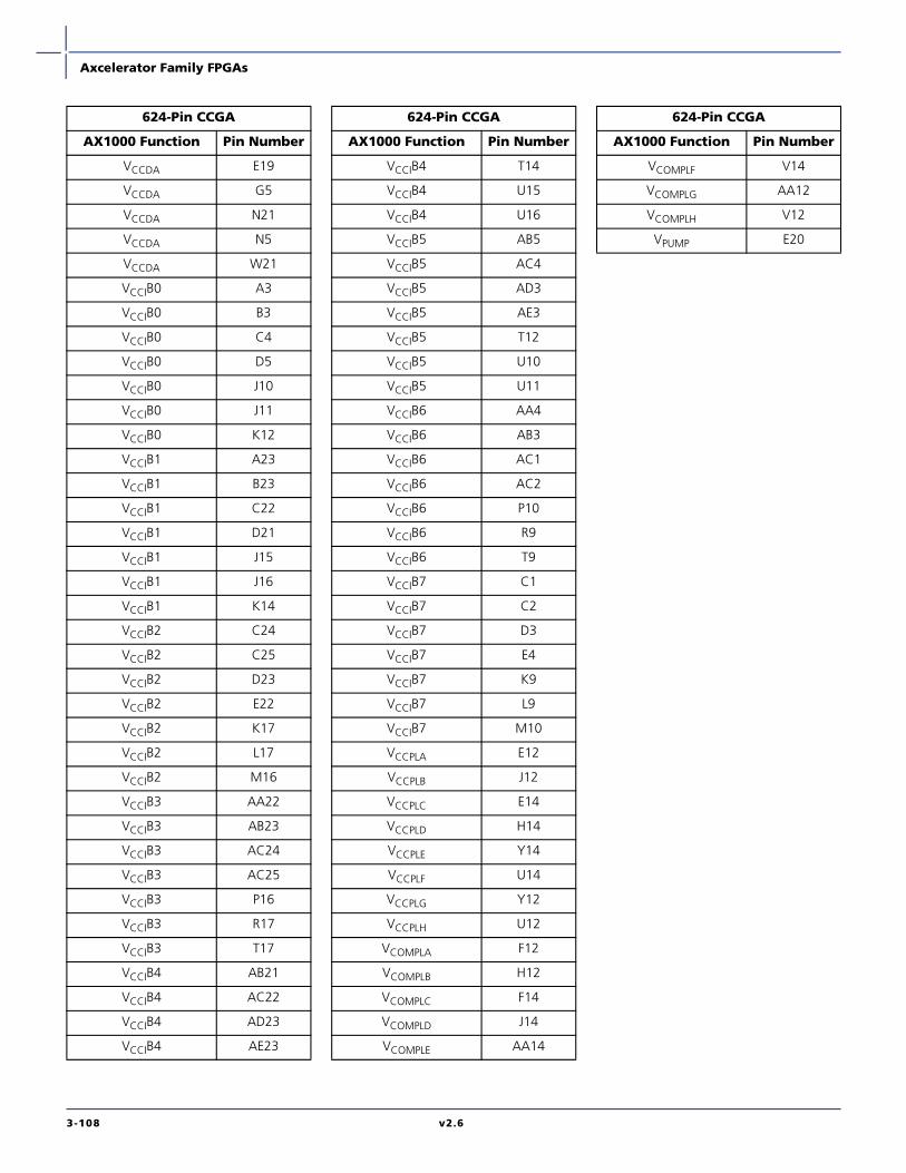
Axcelerator Family FPGAs
3-108 v2.6
VCCDA E19
VCCDA G5
VCCDA N21
VCCDA N5
VCCDA W21
VCCIB0 A3
VCCIB0 B3
VCCIB0 C4
VCCIB0 D5
VCCIB0 J10
VCCIB0 J11
VCCIB0 K12
VCCIB1 A23
VCCIB1 B23
VCCIB1 C22
VCCIB1 D21
VCCIB1 J15
VCCIB1 J16
VCCIB1 K14
VCCIB2 C24
VCCIB2 C25
VCCIB2 D23
VCCIB2 E22
VCCIB2 K17
VCCIB2 L17
VCCIB2 M16
VCCIB3 AA22
VCCIB3 AB23
VCCIB3 AC24
VCCIB3 AC25
VCCIB3 P16
VCCIB3 R17
VCCIB3 T17
VCCIB4 AB21
VCCIB4 AC22
VCCIB4 AD23
VCCIB4 AE23
624-Pin CCGA
AX1000 Function Pin Number
VCCIB4 T14
VCCIB4 U15
VCCIB4 U16
VCCIB5 AB5
VCCIB5 AC4
VCCIB5 AD3
VCCIB5 AE3
VCCIB5 T12
VCCIB5 U10
VCCIB5 U11
VCCIB6 AA4
VCCIB6 AB3
VCCIB6 AC1
VCCIB6 AC2
VCCIB6 P10
VCCIB6 R9
VCCIB6 T9
VCCIB7 C1
VCCIB7 C2
VCCIB7 D3
VCCIB7 E4
VCCIB7 K9
VCCIB7 L9
VCCIB7 M10
VCCPLA E12
VCCPLB J12
VCCPLC E14
VCCPLD H14
VCCPLE Y14
VCCPLF U14
VCCPLG Y12
VCCPLH U12
VCOMPLA F12
VCOMPLB H12
VCOMPLC F14
VCOMPLD J14
VCOMPLE AA14
624-Pin CCGA
AX1000 Function Pin Number
VCOMPLF V14
VCOMPLG AA12
VCOMPLH V12
VPUMP E20
624-Pin CCGA
AX1000 Function Pin Number
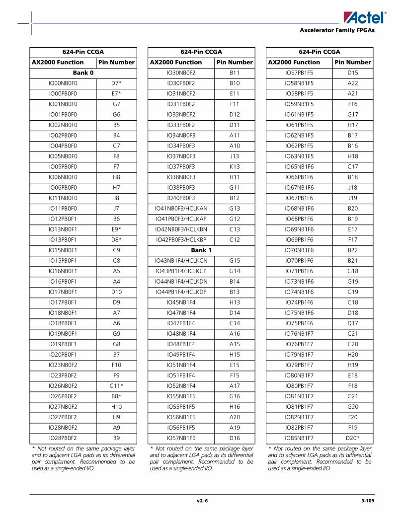
Axcelerator Family FPGAs
v2.6 3-109
624-Pin CCGA
AX2000 Function Pin Number
Bank 0
IO00NB0F0 D7*
IO00PB0F0 E7*
IO01NB0F0 G7
IO01PB0F0 G6
IO02NB0F0 B5
IO02PB0F0 B4
IO04PB0F0 C7
IO05NB0F0 F8
IO05PB0F0 F7
IO06NB0F0 H8
IO06PB0F0 H7
IO11NB0F0 J8
IO11PB0F0 J7
IO12PB0F1 B6
IO13NB0F1 E9*
IO13PB0F1 D8*
IO15NB0F1 C9
IO15PB0F1 C8
IO16NB0F1 A5
IO16PB0F1 A4
IO17NB0F1 D10
IO17PB0F1 D9
IO18NB0F1 A7
IO18PB0F1 A6
IO19NB0F1 G9
IO19PB0F1 G8
IO20PB0F1 B7
IO23NB0F2 F10
IO23PB0F2 F9
IO26NB0F2 C11*
IO26PB0F2 B8*
IO27NB0F2 H10
IO27PB0F2 H9
IO28NB0F2 A9
IO28PB0F2 B9
* Not routed on the same package layerand to adjacent LGA pads as its differentialpair complement. Recommended to beused as a single-ended I/O.
IO30NB0F2 B11
IO30PB0F2 B10
IO31NB0F2 E11
IO31PB0F2 F11
IO33NB0F2 D12
IO33PB0F2 D11
IO34NB0F3 A11
IO34PB0F3 A10
IO37NB0F3 J13
IO37PB0F3 K13
IO38NB0F3 H11
IO38PB0F3 G11
IO40PB0F3 B12
IO41NB0F3/HCLKAN G13
IO41PB0F3/HCLKAP G12
IO42NB0F3/HCLKBN C13
IO42PB0F3/HCLKBP C12
Bank 1
IO43NB1F4/HCLKCN G15
IO43PB1F4/HCLKCP G14
IO44NB1F4/HCLKDN B14
IO44PB1F4/HCLKDP B13
IO45NB1F4 H13
IO47NB1F4 D14
IO47PB1F4 C14
IO48NB1F4 A16
IO48PB1F4 A15
IO49PB1F4 H15
IO51NB1F4 E15
IO51PB1F4 F15
IO52NB1F4 A17
IO55NB1F5 G16
IO55PB1F5 H16
IO56NB1F5 A20
IO56PB1F5 A19
IO57NB1F5 D16
624-Pin CCGA
AX2000 Function Pin Number
* Not routed on the same package layerand to adjacent LGA pads as its differentialpair complement. Recommended to beused as a single-ended I/O.
IO57PB1F5 D15
IO58NB1F5 A22
IO58PB1F5 A21
IO59NB1F5 F16
IO61NB1F5 G17
IO61PB1F5 H17
IO62NB1F5 B17
IO62PB1F5 B16
IO63NB1F5 H18
IO65NB1F6 C17
IO66PB1F6 B18
IO67NB1F6 J18
IO67PB1F6 J19
IO68NB1F6 B20
IO68PB1F6 B19
IO69NB1F6 E17
IO69PB1F6 F17
IO70NB1F6 B22
IO70PB1F6 B21
IO71PB1F6 G18
IO73NB1F6 G19
IO74NB1F6 C19
IO74PB1F6 C18
IO75NB1F6 D18
IO75PB1F6 D17
IO76NB1F7 C21
IO76PB1F7 C20
IO79NB1F7 H20
IO79PB1F7 H19
IO80NB1F7 E18
IO80PB1F7 F18
IO81NB1F7 G21
IO81PB1F7 G20
IO82NB1F7 F20
IO82PB1F7 F19
IO85NB1F7 D20*
624-Pin CCGA
AX2000 Function Pin Number
* Not routed on the same package layerand to adjacent LGA pads as its differentialpair complement. Recommended to beused as a single-ended I/O.

Axcelerator Family FPGAs
3-110 v2.6
IO85PB1F7 D19*
Bank 2
IO86NB2F8 F23
IO86PB2F8 E23
IO87NB2F8 H23
IO87PB2F8 G23
IO88NB2F8 E24
IO88PB2F8 D24
IO89NB2F8 M17*
IO89PB2F8 G22*
IO91NB2F8 J22
IO91PB2F8 H22
IO92NB2F8 L18
IO92PB2F8 K18
IO96NB2F9 G24
IO96PB2F9 F24
IO97NB2F9 J21
IO97PB2F9 J20
IO98PB2F9 J23
IO99NB2F9 L19
IO99PB2F9 K19
IO100NB2F9 E25
IO100PB2F9 D25
IO103PB2F9 K20
IO105NB2F9 M19
IO105PB2F9 M18
IO106NB2F9 J24
IO106PB2F9 H24
IO107NB2F10 L23*
IO107PB2F10 N16*
IO109NB2F10 L22
IO109PB2F10 K22
IO110NB2F10 G25
IO110PB2F10 F25
IO111NB2F10 L21
IO111PB2F10 L20
624-Pin CCGA
AX2000 Function Pin Number
* Not routed on the same package layerand to adjacent LGA pads as its differentialpair complement. Recommended to beused as a single-ended I/O.
IO112NB2F10 L24
IO112PB2F10 K24
IO113NB2F10 N17
IO115NB2F10 M20
IO115PB2F10 M21
IO117NB2F10 N19
IO117PB2F10 N18
IO118NB2F11 J25
IO121NB2F11 N24
IO121PB2F11 M24
IO122NB2F11 L25
IO122PB2F11 K25
IO123NB2F11 N22
IO123PB2F11 M22
IO124NB2F11 N23
IO124PB2F11 M23
IO127NB2F11 P18
IO127PB2F11 P17
IO128NB2F11 N25
IO128PB2F11 M25
Bank 3
IO129NB3F12 N20
IO130PB3F12 P24
IO131NB3F12 P21
IO133NB3F12 P20
IO133PB3F12 P19
IO138NB3F12 R23
IO138PB3F12 P23
IO139NB3F13 R22
IO139PB3F13 P22
IO141NB3F13 R19
IO142NB3F13 R25
IO142PB3F13 P25
IO143PB3F13 R21
IO145NB3F13 T18
IO145PB3F13 R18
624-Pin CCGA
AX2000 Function Pin Number
* Not routed on the same package layerand to adjacent LGA pads as its differentialpair complement. Recommended to beused as a single-ended I/O.
IO146NB3F13 T24
IO146PB3F13 R24
IO147NB3F13 T20
IO147PB3F13 R20
IO148NB3F13 U25
IO148PB3F13 T25
IO149NB3F13 T22
IO153NB3F14 U19
IO153PB3F14 T19
IO154NB3F14 Y25
IO154PB3F14 W25
IO157NB3F14 V20
IO157PB3F14 U20
IO158NB3F14 AB25
IO158PB3F14 AA25
IO160PB3F14 W24
IO161NB3F15 U24
IO161PB3F15 U23
IO162NB3F15 AA24
IO162PB3F15 Y24
IO163NB3F15 V22
IO163PB3F15 U22
IO164NB3F15 V23
IO164PB3F15 V24
IO166NB3F15 AB24
IO167NB3F15 V21
IO167PB3F15 U21
IO168NB3F15 Y23
IO168PB3F15 AA23
IO169NB3F15 W22*
IO169PB3F15 W23*
IO170NB3F15 Y22
IO170PB3F15 Y21
Bank 4
IO171NB4F16 AC20*
IO171PB4F16 AC21*
624-Pin CCGA
AX2000 Function Pin Number
* Not routed on the same package layerand to adjacent LGA pads as its differentialpair complement. Recommended to beused as a single-ended I/O.

Axcelerator Family FPGAs
v2.6 3-111
IO172NB4F16 W20
IO172PB4F16 Y20
IO173NB4F16 AD21
IO173PB4F16 AD22
IO174NB4F16 AA19
IO176NB4F16 Y18
IO176PB4F16 Y19
IO177NB4F16 AB19
IO177PB4F16 AB18
IO182NB4F17 V19
IO182PB4F17 W19
IO183PB4F17 AC19
IO184NB4F17 AB17
IO184PB4F17 AC17
IO185NB4F17 AD19
IO185PB4F17 AD20
IO187PB4F17 AC18
IO188NB4F17 Y17
IO188PB4F17 AA17
IO189PB4F17 AE22
IO191NB4F17 W18
IO191PB4F17 V18
IO192PB4F17 U18
IO195PB4F18 AE21
IO196NB4F18 AB16
IO197NB4F18 AD17
IO197PB4F18 AD18
IO198NB4F18 V17
IO198PB4F18 W17
IO199NB4F18 AE19
IO199PB4F18 AE20
IO200NB4F18 AC15
IO201NB4F18 AD15
IO201PB4F18 AD16
IO202NB4F18 Y15
IO202PB4F18 Y16
624-Pin CCGA
AX2000 Function Pin Number
* Not routed on the same package layerand to adjacent LGA pads as its differentialpair complement. Recommended to beused as a single-ended I/O.
IO206NB4F19 AB14
IO206PB4F19 AB15
IO207NB4F19 AE15
IO207PB4F19 AE16
IO208PB4F19 W16
IO209NB4F19 AE14
IO210NB4F19 V15
IO210PB4F19 V16
IO211NB4F19 AD14
IO211PB4F19 AC14
IO212NB4F19/CLKEN W14
IO212PB4F19/CLKEP W15
IO213NB4F19/CLKFN AC13
IO213PB4F19/CLKFP AD13
Bank 5
IO214NB5F20/CLKGN W13
IO214PB5F20/CLKGP Y13
IO215NB5F20/CLKHN AC12
IO215PB5F20/CLKHP AD12
IO216NB5F20 U13
IO216PB5F20 V13
IO217NB5F20 AE10
IO217PB5F20 AE11
IO218NB5F20 W11
IO218PB5F20 W12
IO222NB5F20 AA11
IO222PB5F20 Y11
IO223PB5F21 AE9
IO225NB5F21 AE6
IO225PB5F21 AE7
IO226NB5F21 Y10
IO226PB5F21 W10
IO227PB5F21 T13
IO228NB5F21 AB10
IO228PB5F21 AB11
IO229NB5F21 AD9
624-Pin CCGA
AX2000 Function Pin Number
* Not routed on the same package layerand to adjacent LGA pads as its differentialpair complement. Recommended to beused as a single-ended I/O.
IO229PB5F21 AD10
IO230NB5F21 V11
IO233NB5F21 AD7
IO233PB5F21 AD8
IO234NB5F21 V9
IO234PB5F21 V10
IO236NB5F22 AC9
IO238NB5F22 W8
IO238PB5F22 W9
IO239NB5F22 AE4
IO239PB5F22 AE5
IO240NB5F22 AB9
IO242NB5F22 AA9
IO242PB5F22 Y9
IO243NB5F22 AD5
IO243PB5F22 AD6
IO244NB5F22 U8
IO246NB5F23 AB8
IO246PB5F23 AC8
IO247NB5F23 AB7
IO247PB5F23 AC7
IO250NB5F23 AA8
IO250PB5F23 Y8
IO251NB5F23 V8
IO251PB5F23 V7
IO252NB5F23 Y7
IO252PB5F23 W7
IO253NB5F23 AC5
IO253PB5F23 AC6
IO254NB5F23 Y6
IO254PB5F23 W6
IO256NB5F23 AB6*
IO256PB5F23 AA6*
Bank 6
IO257NB6F24 Y3
IO257PB6F24 AA3
624-Pin CCGA
AX2000 Function Pin Number
* Not routed on the same package layerand to adjacent LGA pads as its differentialpair complement. Recommended to beused as a single-ended I/O.

Axcelerator Family FPGAs
3-112 v2.6
IO258NB6F24 V3
IO258PB6F24 W3
IO259NB6F24 AA2
IO259PB6F24 AB2
IO260NB6F24 V6*
IO260PB6F24 W4*
IO262NB6F24 U4
IO262PB6F24 V4
IO263NB6F24 Y5
IO263PB6F24 W5
IO268NB6F25 U6
IO268PB6F25 U5
IO269PB6F25 U3
IO272NB6F25 T2
IO272PB6F25 U2
IO273NB6F25 W2
IO273PB6F25 Y2
IO274NB6F25 R6
IO274PB6F25 T6
IO275NB6F25 T7
IO275PB6F25 U7
IO277NB6F25 V2
IO278NB6F26 R4
IO278PB6F26 T4
IO279PB6F26 R3
IO280NB6F26 R5
IO281NB6F26 AA1
IO281PB6F26 AB1
IO284NB6F26 R8
IO284PB6F26 T8
IO285NB6F26 W1
IO285PB6F26 Y1
IO286NB6F26 P2
IO286PB6F26 R2
IO287NB6F26 T1
IO287PB6F26 U1
624-Pin CCGA
AX2000 Function Pin Number
* Not routed on the same package layerand to adjacent LGA pads as its differentialpair complement. Recommended to beused as a single-ended I/O.
IO288NB6F26 P5
IO290NB6F27 P6
IO291NB6F27 P1
IO291PB6F27 R1
IO292NB6F27 P7
IO292PB6F27 R7
IO293NB6F27 M1
IO293PB6F27 N1
IO294NB6F27 P8
IO296NB6F27 N3
IO296PB6F27 P3
IO298NB6F27 N4
IO298PB6F27 P4
IO299NB6F27 M2
IO299PB6F27 N2
Bank 7
IO300NB7F28 P9*
IO300PB7F28 N6*
IO302NB7F28 M6
IO304NB7F28 N8
IO304PB7F28 N7
IO308NB7F28 M4
IO309NB7F28 L3
IO309PB7F28 M3
IO310NB7F29 N10
IO310PB7F29 N9
IO311NB7F29 K1
IO311PB7F29 L1
IO313NB7F29 M5
IO316NB7F29 L6
IO316PB7F29 L5
IO317NB7F29 K2
IO317PB7F29 L2
IO318NB7F29 K4
IO318PB7F29 L4
IO320NB7F29 J3
624-Pin CCGA
AX2000 Function Pin Number
* Not routed on the same package layerand to adjacent LGA pads as its differentialpair complement. Recommended to beused as a single-ended I/O.
IO321NB7F30 J2
IO321PB7F30 J1
IO323NB7F30 L7
IO323PB7F30 M7
IO324NB7F30 M9
IO324PB7F30 M8
IO327NB7F30 F1
IO327PB7F30 G1
IO328NB7F30 K7
IO328PB7F30 K6
IO329NB7F30 D1
IO329PB7F30 E1
IO331PB7F30 G2
IO332NB7F31 H3
IO332PB7F31 H2
IO333NB7F31 E2
IO333PB7F31 F2
IO334NB7F31 H4
IO334PB7F31 J4
IO335NB7F31 H5
IO335PB7F31 H6
IO337NB7F31 D2
IO338NB7F31 J6
IO338PB7F31 J5
IO339NB7F31 F3
IO339PB7F31 E3
IO340NB7F31 G4*
IO340PB7F31 G3*
IO341NB7F31 K8
IO341PB7F31 L8
Dedicated I/O
GND K5
GND A18
GND A2
GND A24
GND A25
624-Pin CCGA
AX2000 Function Pin Number
* Not routed on the same package layerand to adjacent LGA pads as its differentialpair complement. Recommended to beused as a single-ended I/O.

Axcelerator Family FPGAs
v2.6 3-113
GND A8
GND AA10
GND AA16
GND AA18
GND AA21
GND AA5
GND AB22
GND AB4
GND AC10
GND AC16
GND AC23
GND AC3
GND AD1
GND AD2
GND AD24
GND AD25
GND AE1
GND AE18
GND AE2
GND AE24
GND AE25
GND AE8
GND B1
GND B2
GND B24
GND B25
GND C10
GND C16
GND C23
GND C3
GND D22
GND D4
GND E10
GND E16
GND E21
GND E5
624-Pin CCGA
AX2000 Function Pin Number
* Not routed on the same package layerand to adjacent LGA pads as its differentialpair complement. Recommended to beused as a single-ended I/O.
GND E8
GND H1
GND H21
GND H25
GND K21
GND K23
GND K3
GND L11
GND L12
GND L13
GND L14
GND L15
GND M11
GND M12
GND M13
GND M14
GND M15
GND N11
GND N12
GND N13
GND N14
GND N15
GND P11
GND P12
GND P13
GND P14
GND P15
GND R11
GND R12
GND R13
GND R14
GND R15
GND T21
GND T23
GND T3
GND T5
624-Pin CCGA
AX2000 Function Pin Number
* Not routed on the same package layerand to adjacent LGA pads as its differentialpair complement. Recommended to beused as a single-ended I/O.
GND V1
GND V25
GND V5
PRA F13
PRB A13
PRC AB12
PRD AE13
TCK F5
TDI C5
TDO F6
TMS D6
TRST E6
VCCA AB20
VCCA F22
VCCA F4
VCCA J17
VCCA J9
VCCA K10
VCCA K11
VCCA K15
VCCA K16
VCCA L10
VCCA L16
VCCA R10
VCCA R16
VCCA T10
VCCA T11
VCCA T15
VCCA T16
VCCA U17
VCCA U9
VCCA Y4
VCCDA A12
VCCDA A14
VCCDA AA13
VCCDA AA15
624-Pin CCGA
AX2000 Function Pin Number
* Not routed on the same package layerand to adjacent LGA pads as its differentialpair complement. Recommended to beused as a single-ended I/O.
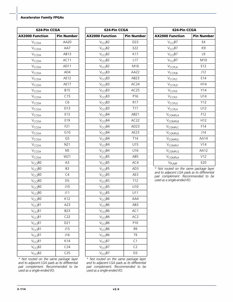
Axcelerator Family FPGAs
3-114 v2.6
VCCDA AA20
VCCDA AA7
VCCDA AB13
VCCDA AC11
VCCDA AD11
VCCDA AD4
VCCDA AE12
VCCDA AE17
VCCDA B15
VCCDA C15
VCCDA C6
VCCDA D13
VCCDA E13
VCCDA E19
VCCDA F21
VCCDA G10
VCCDA G5
VCCDA N21
VCCDA N5
VCCDA W21
VCCIB0 A3
VCCIB0 B3
VCCIB0 C4
VCCIB0 D5
VCCIB0 J10
VCCIB0 J11
VCCIB0 K12
VCCIB1 A23
VCCIB1 B23
VCCIB1 C22
VCCIB1 D21
VCCIB1 J15
VCCIB1 J16
VCCIB1 K14
VCCIB2 C24
VCCIB2 C25
624-Pin CCGA
AX2000 Function Pin Number
* Not routed on the same package layerand to adjacent LGA pads as its differentialpair complement. Recommended to beused as a single-ended I/O.
VCCIB2 D23
VCCIB2 E22
VCCIB2 K17
VCCIB2 L17
VCCIB2 M16
VCCIB3 AA22
VCCIB3 AB23
VCCIB3 AC24
VCCIB3 AC25
VCCIB3 P16
VCCIB3 R17
VCCIB3 T17
VCCIB4 AB21
VCCIB4 AC22
VCCIB4 AD23
VCCIB4 AE23
VCCIB4 T14
VCCIB4 U15
VCCIB4 U16
VCCIB5 AB5
VCCIB5 AC4
VCCIB5 AD3
VCCIB5 AE3
VCCIB5 T12
VCCIB5 U10
VCCIB5 U11
VCCIB6 AA4
VCCIB6 AB3
VCCIB6 AC1
VCCIB6 AC2
VCCIB6 P10
VCCIB6 R9
VCCIB6 T9
VCCIB7 C1
VCCIB7 C2
VCCIB7 D3
624-Pin CCGA
AX2000 Function Pin Number
* Not routed on the same package layerand to adjacent LGA pads as its differentialpair complement. Recommended to beused as a single-ended I/O.
VCCIB7 E4
VCCIB7 K9
VCCIB7 L9
VCCIB7 M10
VCCPLA E12
VCCPLB J12
VCCPLC E14
VCCPLD H14
VCCPLE Y14
VCCPLF U14
VCCPLG Y12
VCCPLH U12
VCOMPLA F12
VCOMPLB H12
VCOMPLC F14
VCOMPLD J14
VCOMPLE AA14
VCOMPLF V14
VCOMPLG AA12
VCOMPLH V12
VPUMP E20
624-Pin CCGA
AX2000 Function Pin Number
* Not routed on the same package layerand to adjacent LGA pads as its differentialpair complement. Recommended to beused as a single-ended I/O.

Axcelerator Family FPGAs
v2.6 4-1
Datasheet Information
List of ChangesThe following table lists critical changes that were made in the current version of the document.
Previous Version Changes in Current Version (v2.6) Page
v2.5 In Table 2-4, the units for the PLOAD, P10, and PI/O were updated from mW/MHz to mW/MHz. 2-2
In the "Pin Descriptions"section, the HCLK and CLK descriptions were updated to include tie-offinformation.
2-9
The "Global Resource Distribution" section was updated. 2-59
The " 624-Pin CCGA" table was updated. 3-103
v2.4 A note was added to Table 2-2. 2-1
In the "Package Thermal Characteristics", the temperature was changed from 150°C to 125°C. 2-6
v2.3 Revised ordering information and timing data to reflect phase out of –3 speed grade options.
Table 2-3 was updated. 2
v2.2 The "Packaging Data" section is new. iii
Table 2-2 was updated. 2-1
"VCCDA Supply Voltage" was updated. 2-9
"PRA/B/C/D Probe A/B/C/D" was updated. 2-10
The "User I/Os" was updated. 2-10
v2.1 Figure 1-3 was updated. 1-3
Table 2-2 was updated. 2-1
The "Power-Up/Down Sequence" section was updated. 2-1
Table 2-4 was updated. 2-2
Table 2-5 was updated. 2-3
The "Timing Characteristics" section was added. 2-7
Table 2-7 was updated. 2-7
Figure 2-1 was updated. 2-8
The External Setup and Clock-to-Out (Pad-to-Pad) equations in the "Hardwired Clock – UsingLVTTL 24mA High Slew Clock I/O" section were updated.
2-8
The External Setup and Clock-to-Out (Pad-to-Pad) in the "Routed Clock – Using LVTTL 24mAHigh Slew Clock I/O" section were updated.
2-8
The "Global Pins" section was updated. 2-9
The "User I/Os" section was updated. 2-10
Table 2-17 was updated. 2-17
Figure 2-8 was updated. 2-18
Figure 2-13 and Figure 2-14 were updated. 2-21

Axcelerator Family FPGAs
4-2 v2.6
v2.1 (continued) The following timing parameters were renamed in I/O timing characteristic tables fromTable 2-21 to Table 2-59:
tIOCLKQ > tICLKQ
tIOCLKY > tOCLKQ
2-22 to 2-41
Timing numbers were updated from Table 2-21 to Table 2-77. 2-22 to 2-58
The "R-Cell" section was updated. 2-47
Figure 2-59 was updated. 2-74
Figure 2-60 was updated. 2-75
Figure 2-67 was updated. 2-85
Figure 2-68 was updated. 2-86
Table 2-88 to Table 2-92 were updated. 2-75 to 2-79
Table 2-97 to Table 2-101 were updated. 2-86 to 2-88
The "TRST" section was updated. 2-89
The "Global Set Fuse" section was added. 2-90
A footnote was added to "896-Pin FBGA" for the AX2000 regarding pins AB1, AE2, G1, andK2.
3-49
Pinouts for the AX250, AX500 and AX1000 were added for "352-Pin CQFP". 3-88
Pinout for the AX1000 was added for "624-Pin CCGA". 3-102
v2.0 Table 2-78 was updated. 2-58
The "Low Power Mode" section was updated. 2-89
Advanced v1.6 Table 1-1 has been updated. i
"Ordering Information" section has been updated. ii
The "Device Resources" section has been updated. ii
The "Temperature Grade Offerings" section is new. iii
The "Speed Grade and Temperature Grade Matrix" section has been updated. iii
Table 2-9 has been updated. 2-11
Table 2-10 has been updated. 2-11
Table 2-1 has been updated. 2-1
Table 2-2 has been updated. 2-1
Table 2-3 has been updated. 2-2
Table 2-4 has been updated. 2-2
Table 2-5 has been updated. 2-3
The "Power Estimation Example" section has been updated. 2-5
The "Thermal Characteristics" section has been updated. 2-6
The "Package Thermal Characteristics" section has been updated. 2-6
The "Timing Characteristics" section has been updated. 2-7
The "Pin Descriptions" section has been updated. 2-9
Timing numbers have been updated from the "3.3V LVTTL" section to the "TimingCharacteristics" section. Many AC Loads were updated as well.
2-22 to 2-48
Timing characteristics for the "Hardwired Clocks" section were updated. 2-55
Previous Version Changes in Current Version (v2.6) Page

Axcelerator Family FPGAs
v2.6 4-3
Timing characteristics for the "Routed Clocks" section were updated. 2-57
Table 2-88 to Table 2-91 were updated. 2-75 to 2-78
Table 2-97 to Table 2-98were updated. 2-86 to 2-87
The "Low Power Mode" section was updated. 2-89
The "Interface" section was updated. 2-89
The "Data Registers (DRs)" section was updated. 2-90
The "Security" section was updated. 2-90
Advanced v0.6 The "Silicon Explorer II Probe Interface" section was updated. 2-91
(continued) The "Programming" section was updated. 2-91
In the "208-Pin PQFP" (AX500) section, pins 2, 52, and 156 changed from VCCDA to VCCA.For pins 170 and 171, the I/O names refer to pair 23 instead of 24.
3-78
The following changes were made in the "676-Pin FBGA"(AX500) section:AE2, AE25 Change from NC to GND.AF2, AF25 Changed from GND to NCAB4, AF24, C1, C26 Changed from VCCDA to VCCAAD15 Change from VCCDA to VCOMPLEAD17 Changed from VCOMPLE to VCCDA
3-36
In the "896-Pin FBGA" (AX2000) section, the AK28 changed from VCCIB5 to VCCIB4. 3-49
The "352-Pin CQFP" section is new. 3-88
The "624-Pin CCGA" section is new. 3-102
Advanced v1.5 All I/O FIFO capability was removed. n/a
Table 1-1 was updated. i
Figure 1-9 and was updated. 1-7
Figure 2-5 was updated. 2-14
The "Using an I/O Register" section was updated. 2-14
The AX250 and AX1000 descriptions were added to the "484-Pin FBGA"section. 3-22
Advanced v1.4 Table 2-3 was updated. 2-2
Figure 2-1 was updated. 2-8
Figure 2-48 was updated. 2-63
Figure 2-52 was updated. 2-68
Advanced v1.3 In the "208-Pin PQFP" table, pin 196 was missing, but it has been added in this version with afunction of GND.
3-78
The following pins in the "484-Pin FBGA" table for AX500 were changed:
Pin G7 is GND/LP
Pins AB8, C10, C11, C14, AB16 are NC.
3-22
The "676-Pin FBGA" table was updated. 3-36
Previous Version Changes in Current Version (v2.6) Page

Axcelerator Family FPGAs
4-4 v2.6
Advanced v1.2 The "Device Resources" section was updated for the CS180. ii
The "Programmable Interconnect Element" and Figure 1-2 was new. 1-1 and 1-2
The "180-Pin CSP" table is new. 3-1
The "208-Pin PQFP" tables for the AX500 were updated. The following pins were not definedin the previous version:
GND 21IO106PB5F10/CLKHP 71GND 136
3-78
Advanced v1.1 Table 1-1 was updated. i
"Ordering Information", "Device Resources" and the Product Plan table were updated. ii
Figure 1-3 was updated. 1-3
The "Design Environment" section was updated. 1-6
Figure 1-8 was new. 1-6
Table 2-3 was updated. 2-2
"Package Thermal Characteristics" was updated. 2-6
Figure 2-2 was updated. 2-9
Table 2-8 was updated. 2-11
Figure 2-11 was updated. 2-20
The timing characteristics tables from pages 2-22 to 2-49 were updated. 2-22 to 2-49
The "Global Resources" section was updated. 2-55
The timing characteristics tables from pages 2-86 to 2-87 were updated. 2-86 to 2-87
The "208-Pin PQFP" tables are new. 3-78
The "256-Pin FBGA" tables are new. 3-12
The "324-Pin FBGA" tables are new. 3-18
Previous Version Changes in Current Version (v2.6) Page

Datasheet CategoriesIn order to provide the latest information to designers, some datasheets are published before data has been fullycharacterized. Datasheets are designated as “Product Brief,” “Advanced,” “Production,” and “Web-only.” Thedefinition of these categories are as follows:
Product BriefThe product brief is a summarized version of a advanced datasheet (advanced or production) containing generalproduct information. This brief gives an overview of specific device and family information.
AdvancedThis datasheet version contains initial estimated information based on simulation, other products, devices, or speedgrades. This information can be used as estimates, but not for production.
Datasheet SupplementThe datasheet supplement gives specific device information for a derivative family that differs from the general familydatasheet. The supplement is to be used in conjunction with the datasheet to obtain more detailed information andfor specifications that do not differ between the two families.
Unmarked (production) This datasheet version contains information that is considered to be final.
Export Administration Regulations (EAR) The products described in this datasheet are subject to the Export Administration Regulations (EAR). They couldrequire an approved export license prior to export from the United States. An export includes release of product ordisclosure of technology to a foreign national inside or outside the United States.

5172160-14/12.05
http://www.actel.com
Actel and the Actel logo are registered trademarks of Actel Corporation.All other trademarks are the property of their owners.
Actel Corporation
2061 Stierlin CourtMountain View, CA94043-4655 USAPhone 650.318.4200Fax 650.318.4600
Actel Europe Ltd.
Dunlop House, Riverside WayCamberley, Surrey GU15 3YLUnited KingdomPhone +44 (0) 1276 401 450Fax +44 (0) 1276 401 490
Actel Japanwww.jp.actel.com
EXOS Ebisu Bldg. 4F1-24-14 Ebisu Shibuya-kuTokyo 150 JapanPhone +81.03.3445.7671Fax +81.03.3445.7668
Actel Hong Kongwww.jp.actel.com
Suite 2114, Two Pacific Place88 Queensway, AdmiraltyHong KongPhone +852 2185 6460Fax +852 2185 6488