Embed Size (px)
Citation preview

1 Prepared By: Nafees Ahmed www.eedofdit.weebly.com
Single Phase Transformer©
By
Nafees Ahmed Asstt. Prof. Department of Electrical Engineering
DIT, University, Dehradun, Uttarakhand
References:
1. V. Del Toro “Principles of electrical engineering” Prentice Hall International
2. B. L Theraja “ Electrical Technology” S. Chand
3. www.google.com
4. www.wikipedia.org

2 Prepared By: Nafees Ahmed www.eedofdit.weebly.com
It is a static device which transfers energy form one electrical circuit to another electrical
circuit without change in frequency. Very high efficiency (up to 96% or up to 98%, Because there is no rotating part)
Types of transformer:
Depending on types of phase 1. 1-ϕ transformer 2. 3- ϕ transformer
Depending on use a. Step up transformer: Output voltage is higher then applied voltage b. Step down transformer: Output voltage is less then applied voltage
Depending of construction 1. Shell type transformer 2. Corel type transformer
Construction and working principle: Construction:
Laminated core of Si-Steel (Soft Steel) Soft Steel is used to reduce hysteresis losses
L V
L V
H V
H V
L V
L V
H V
H V
Figure 1
Core type Shell type
HV
LV
HV
LV
LV
HV
LV
HV
LV
LV
Laminated Core
Primary (LV/HV)
Secondary (HV/LV)
Secondary (HV/LV)
Flux
Figure 2

3 Prepared By: Nafees Ahmed www.eedofdit.weebly.com
Laminated core is to reduced eddy current losses Principle: Based on low of electromagnetic induction. Ideal Transformer: Conditions for ideal transformer are
1. Copper losses are zero: => Winding resistance = 0 2. Iron (Core) losses are zero: => Hysteresis & eddy current losses =0 3. Leakage flux is zero: => Permeability of iron is infinity
=>
4. Magnetizing current is zero EMF Equation: (Prove that emf per turn for a transformer is constant)
Let an alternating voltage (v1) is applied to the primary side So an alternating flux will produce in the core
Let
Because of this an emf will induce in primary as well as in secondary windings Primary induced emf
Or )2(2/11 tSinEe m Where
01
A
lS
dt
dNe
11
)1( tSinm
dt
tSindNe m
11
tCosNe m 11
2/11 tSinNe m
Figure 3: Core type 1-Ph transformer
N1 N2 e1 e2 v1 v2
ϕ

4 Prepared By: Nafees Ahmed www.eedofdit.weebly.com
Constant44.42
2
1
1 mfN
E
N
E
Ksay Constant 1
2
1
2
1
2 N
N
E
E
V
V
K2
1
1
2
1
2
1
2 I
I
N
N
E
E
V
V
So its RMS value
Similarly RMS values of secondary induced emf
For ideal transformer Induced emf in primary (E1) = Applied Voltage (V1) Induced emf in secondary (E2) = Terminal Voltage (V2) From equations (3) & (4) Hence emf/turn = constant Voltage and current transformation ratio: Again from equations (3) & (4) K= Voltage (Current) transformation ratio For ideal transformer Input VA = Output VA V1I1 = V2I2
Hence
Transformer on NO load: Consider an ideal transformer with magnetizing current: Ideal transformer without iron loss:
Im & ϕ will be in same phase V1 & E1 will be equal and opposite
emfinducedofValueMaxNE mm 11
)3(44.4 11 NfE m
1111
1 44.42
2
22Nf
fNNEE m
mmm
)4(44.4 22 NfE m
2
1
1
2
I
I
V
V

5 Prepared By: Nafees Ahmed www.eedofdit.weebly.com
Ideal transformer with iron loss: + a little copper loss No load current (I0) will be very less (2% - 5% of full load current) No load power factor angle (ϕ0) will be very high ( 780 to 870) Im= Magnetizing or wattles component of no load current (I0) Ie= Active or wattfull component of no load current (I0)
No load power Neglecting copper loss Note: No load power factor is very less because ϕ0 is very high. (ϕ0 is high because Ie<<Im)
Im
E1
E2
V1= -E1
ϕ
Figure 4b: Phasor diagram of ideal transformer
Without Iron loss
RI 2
0
V1 E1 R0
X0
I0
Ie Im
I0
Figure 4e: Equivalent Circuit
lossiron Total =010 CosIVP o
00 CosIIe
00 SinIIm
eI
VR 1
0
mI
VX 1
0
Figure 4a
N1 N2 E1 E2 V1 V2
ϕ
Im
Figure 4c
N1 N2 E1 E2 V1 V2
ϕ
I0
Im=I0Sinϕ0
E1
E2
V1= -E1
ϕ
Figure 4d: Phasor diagram of ideal transformer
with Iron loss
Φ0 Ie=I0Cosϕ0
I0

6 Prepared By: Nafees Ahmed www.eedofdit.weebly.com
22
'
11 ININ
Transformer on load:
MMF induced in primary winding =MMF induced in secondary winding
Note: I1
’ and I2 will be in phase opposition Load may be pure resistive, inductive or capacitive resulting in unity, lagging and leading
power factor respectively. So the phasor diagram may be on unity, lagging and leading power factor.
Resistance and leakage reactance: In transformer windings do have some resistance Let R1 = Resistance of primary winding
R2 = Resistance of secondary winding The flux which is linked with primary as well as secondary windings is known as common flux.
Figure 5a
N1 N2 E1 E2 V1 V2
ϕ
I1 =I0 + I1’
L
O
A
D
I2
22
1
2'
1 KIIN
NI
E1
E2=V2
V1= -E1
ϕ
Figure 5c: Phasor diagram at lagging PF
Φ0 I0
I1
Φ1
I2
I1’ =KI2
Φ2
E1
E2=V2
V1= -E1
ϕ
Figure 5b: Phasor diagram at Unity PF
Φ0 I0
I1 I1
’ =KI2
Φ1
I2 Φ2=0 E1
E2=V2
V1= -E1
ϕ
Figure 5d: Phasor diagram at leading PF
Φ0 I0
I1
Φ1
I2
I1’ =KI2
Φ2

7 Prepared By: Nafees Ahmed www.eedofdit.weebly.com
There is some flux which does not link with primary or secondary winding know as leakage flux as shown in figure 6a. Let ϕL1 = leakage flux of primary winding (Flux which does not link with secondary winding)
ϕL2 = leakage flux of secondary winding (Flux which does not link with primary winding)
So at no load I1 & I2 both are negligible hence leakage flux is negligible. Leakage flux produces a self induced back emf in their respective windings. They are
therefore equivalent to small reactance in series with the respective windings. This reactance is known as leakage reactance.
Let X1 = Leakage reactance of primary winding X2 = Leakage reactance of secondary winding
Note: V1≠ E1 & V2 ≠ E2 as we are taking previously.
2211 IandI LL
Figure 6a
V1 V2
Common Flux
I1
L
O
A
D
I2
Leakage Flux
R1 R2
V1 V2
I1
L
O
A
D
I2 R1 R2
E1 R0 X0
I1’
Ie Im
I0
Figure 6c: Equivalent Circuit
E2
X2 X1
Figure 6b
V1 V2
Common Flux
I1
L
O
A
D
I2 R1 R2
E1 N1 E2 N2
X1 X2
8 Prepared By: Nafees Ahmed www.eedofdit.weebly.com
Phasor diagram of actual transformer ON Load: Load may be pure resistive load( Unity power factor), inductive load (Lagging power factor) and capacitive load (Leading power factor) so as the phasor diagram.
1. Phasor diagram for pure resistive load (at unity power factor):
Note:
a. Resistive drop I2R2 is parallel to I2 and inductive drop I2X2 is perpendicular (leading) to I2.
b. Similarly resistive drop I1R1 is parallel to I1 and inductive drop I1X1 is perpendicular (leading) to I1.
Figure 7a
V1 V2
Common Flux
I1
L
O
A
D
I2 R1 R2
E1 N1 E2 N2
X1 X2
E1
E2=V2
-E1
ϕ
Figure 7b: Phasor diagram at Unity PF
Φ0 I0
I1 I1
’ =KI2
Φ1
I2
Φ2=0
V2 I2R2
I2X2
V1
I1R1
I1X1

9 Prepared By: Nafees Ahmed www.eedofdit.weebly.com
c. This is also true for rest of following two diagrams (lagging and leading pf). If we neglect I1R1, I1X1 and I2R2, I2X2 drops, then
Φ1 = Φ2 = Φ1’= 0 or say Φ
Neglecting 21111 SinRICosXI
2. Phasor diagram for inductive load (at lagging power factor):
222
2
2222 XIRIVE
2222 RIVE
K
EE 2
1
2
1111
2
111111 SinRICosXISinRICosRIEV
SinRICosRIEV 111111
01111 RIEV
E1
E2=V2
-E1
ϕ
Figure 7c: Phasor diagram at lagging PF
Φ0 I0
I1’ =KI2
Φ1
I2
Φ2
V2 I2R2
I2X2
V1
I1R1
I1X1
I1

10 Prepared By: Nafees Ahmed www.eedofdit.weebly.com
If we neglect I1R1, I1X1 and I2R2, I2X2 drops, then
Φ1 = Φ2 = Φ1’= Φ (say)
Neglecting 21111 SinRICosXI
3. Phasor diagram for capacitive load (at leading power factor):
If we neglect I1R1, I1X1 and I2R2, I2X2 drops, then Φ1 = Φ2 = Φ1
’= Φ (say)
2222222
2
22222222 SinRICosXISinXICosRIVE
22222222222222 neglecting SinRICosXISinXICosRIVE
K
EE 2
1
2
1111
2
111111 SinRICosXISinRICosRIEV
SinRICosRIEV 111111
E1
E2=V2
-E1
ϕ
Figure 7d: Phasor diagram at leading PF
Φ0 I0
I1’ =KI2
Φ1
I2
Φ2
V2
I2R2
I2X2
V1 I1R1
I1X1 I1
2222222
2
22222222 SinRICosXISinXICosRIVE
22222222222222 neglecting SinRICosXISinXICosRIVE

11 Prepared By: Nafees Ahmed www.eedofdit.weebly.com
KI
I
N
N
E
E
V
V
2
1
1
2
1
2
1
2
Neglecting 21111 SinRICosXI
Note: The above results can be obtained directly if we replace Φ with – Φ in the case of lagging power factor.
Equivalent circuit of transformer:
Let R1 & X1 are resistance and leakage reactance of primary windings and R2 & X2 are resistance and leakage reactance of secondary windings respectively.
We know
K
EE 2
1
21111
2
111111 SinRICosXISinRICosRIEV
SinRICosRIEV 111111
V1 V2
I1
L
O
A
D
I2 R1 R2
E1 R0 X0
I1’
Ie Im
I0
Figure 8a: Transformer Equivalent Circuit
E2
X2 X1
2
2
121
1V
N
NV
KV
V1
I1
L
O
A
D
R1
R0 X0
I1’
Ie Im
I0
Figure 8b: Transformer Equivalent Circuit Referred to primary side
X1
2
2
1
1E
N
NE
2
2
2
1 XN
N
2
2
2
1 RN
N
2
2
1 VN
N
2
1
2 IN
N

12 Prepared By: Nafees Ahmed www.eedofdit.weebly.com
Equivalent resistance and reactance of transformer: Let R1 = Resistance of primary winding
R2 = Resistance of secondary winding X1 = Leakage reactance of primary winding X2 = Leakage reactance of secondary winding I1R1 = Resistive drop in primary winding I2R2 = Resistive drop in secondary winding I1X1 = Reactive drop in primary winding I2X2 = Reactive drop in secondary winding
1. Equivalent resistance and reactance referred to secondary side:
V1
I1
L
O
A
D
R1
R0 X0
I1’
Ie Im
I0
Figure 8c: Approximately Equivalent Circuit Referred to primary side after shifting parallel branch
X1
2
2
1
1E
N
NE
2
2
2
1 XN
N
2
2
2
1 RN
N
2
2
1 VN
N
2
1
2 IN
N
V1
I1
L
O
A
D
R1
Figure 8d: Approximately Equivalent Circuit Referred to primary side after neglecting parallel branch
X1
2
2
2
1 XN
N
2
2
2
1 RN
N
2
2
1 VN
N
2
1
2 IN
N
KV1
I1/K L
O
A
D
K2R1
Figure 9a: Approximately Equivalent Circuit Referred to secondary side
K2X1 R2 X2 I2
V2

13 Prepared By: Nafees Ahmed www.eedofdit.weebly.com
2
2
21
22
2 RIRKI
21
22
2 RRKI
2
2
21
22
2 XIXKI
21
22
2 XXKI
The above circuit is obtained after considering the following relations Total resistive drop
Where R02 = Equivalent resistance referred to secondary side Total reactive drop
Where X02 = Equivalent reactance referred to secondary side
If ϕ = 0
KI
I
N
N
V
V
2
1
1
2
1
2
K
IIKVV 1
212 &
02
2
2 RI
02
2
2 XI
KV1
L
O
A
D
Figure 9b: Approximately & simplified Equivalent Circuit Referred to secondary side
X02 R02 I2
V2
2022022
2
02202221 SinRICosXISinXICosRIVKV
SinRICosXINeglectingSinXICosRIVKV 02202202202221
SinXICosRIKVV 02202212
02212 RIKVV
ϕ I2 I2R02
I2X02
KV1
V2
Figure 9c: Phasor Diagram (Assuming lagging load)
14 Prepared By: Nafees Ahmed www.eedofdit.weebly.com
2
2
2
11
2
1 / KRIRI
2
21
2
1 / KRRI
2
2
2
21
2
1 / KXIXI
2
21
2
1 / KXXI
If ϕ = 900
If ϕ is leading Replace ϕ with – ϕ in above equation, so
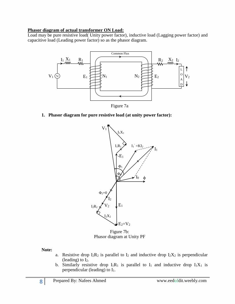
2. Equivalent resistance and reactance referred to primary side:
The above circuit is obtained after considering the following relations
Total resistive drop
Where R01 = Equivalent resistance referred to primary side Total reactive drop
Where X01 = Equivalent reactance referred to primary side
02212 XIKVV
SinXICosRIKVV 02202212
SinXICosRIKVV 02202212
KI
I
N
N
V
V
2
1
1
2
1
2
2121 &1
KIIVK
V
01
2
1 RI
01
2
1 XI
V1
I1
L
O
A
D
R1
Figure 9d: Approximately Equivalent Circuit Referred to primary side
X1
2
2 / KX
2
2 / KR
KV /2
2KI

15 Prepared By: Nafees Ahmed www.eedofdit.weebly.com
If ϕ = 0 If ϕ = 900
If ϕ is leading Replace ϕ with – ϕ in above equation, so
Voltage regulation: It is change in the voltage of secondary side from no load to full load. Let V1 = Full load secondary voltage E2 = No load secondary voltage So % voltage regulation
2011011
2
01101121 / SinRICosXISinXICosRIKVV
SinRICosXINeglectingSinXICosRIKVV 01101101101121 /
0112
1 RIK
VV
0111
1 XIK
VV
SinXICosRIKVV 01101121 /
SinXICosRIKVV 01101121 /
ϕ I1 I1R01
I1X01
V1
V2/K
Figure 9f: Phasor Diagram (Assuming lagging load)
V1
L
O
A
D
Figure 9e: Approximately & simplified Equivalent Circuit Referred to primary side
X01 R01 KI2
V2/K

16 Prepared By: Nafees Ahmed www.eedofdit.weebly.com
1002
22
E
VE
NfBAArea
Em44.4
)(
Where Cos ϕ = Power factor R02 = Equivalent resistance referred to secondary side
X02 = Equivalent reactance referred to secondary side +Ve sign for lagging power factor and –Ve sign for leading power factor.
Condition for zero voltage regulation:
From equation (1) it is clear that voltage regulation will be zero for leading power factor only. So condition of zero voltage regulation
Losses in transformer: The losses are of two type core loss and copper loss
(1) Core or iron losses: It is also known as fixed losses, again of two type (a) Eddy current losses: Given by
Where Ke = Constant Bm = Maxi value of flux density f = frequency t = thickness of laminations v = Volume of core We know NfE m44.4
Put the value of Bm in equation (1)
100
voltageloadNo
voltageloadFullvoltageloadNo
100sec
2
E
windingindropVoltage
)1(1002
022022
E
SinRICosRI
02
022022
E
SinRICosRI
02
02tanX
R
)1(222 WattvtfBKP mee
NAArea
fAArea
E m
)(44.4
)(
)2(44.4
/
fN
AEBm

17 Prepared By: Nafees Ahmed www.eedofdit.weebly.com
For a given transformer N, A, t and V are constants so
So eddy current losses are independent of frequency.
(b) Hysteresis losses: Given by
Where η = Constant Again put the value of Bm from equation (2) to equation (3)
For a given transformer N, A and V are constants so
So eddy current losses dependent of voltage and frequency both.
(2) Copper Losses: Also know as variable losses because they depend on load current.
R1 = Resistance of primary winding R2 = Resistance of secondary winding I1 = Full load current in primary winding I2 = Full load current in secondary winding
Full load copper losses
Copper losses at x time of full load
vtffN
AEKP ee
22
2
44.4
/
vtEAN
KP ee
22
2
44.4
1
2EPe 2VPe )(VoltageVE
)3( WattfvBP x
mh
fvfN
AEP
x
h
44.4
/
vfEAN
P xx
x
h
1
44.4
1
xx
h fEP 1
x
h fVP 12)(VoltageVE
etcxloadhalfforcurrentloadFull
currentloadAnyxWhere
2
1;
2
2
21
2
1 RIRIPC
CCx PxP 2

18 Prepared By: Nafees Ahmed www.eedofdit.weebly.com
Tests on transformer 1. Open Circuit (OC) test or No load test:
By OC test we can find out Iron losses (Pi) No load current (I0) Cosϕ0, Ie, Im, R0 & X0
Iron losses Pi = Reading of wattmeter (P0) No load current I0 = Reading of Ammeter Let V = Reading of voltmeter P0 = Pi = VI0Cosϕ0
Ie = I0Cosϕ0 Im = I0Sinϕ0
Note:
(i) Rated voltage is applied at LV side. (ii) This test is generally done on LV side (Why?)
2. Short Circuit (SC) test:
By OC test we can find out Copper losses (PC) Equivalent resistance or leakage reactance (R01 & X01 OR R02 & X02)
referred to metering side.
Full load Cu losses PC = Reading of wattmeter (Wsc) Let Short circuit current Isc = Reading of Ammeter
0
0VI
PCos i
eI
VR 0
mI
VX 0&
0201
2 RorRRRIW eqeqscsc
0201 ZorZZZIW eqeqscsc
Figure: 10
A
V
LV HV
1-P
hase A
uto
Auto
Tran
sform
er
Rated Voltage
Wattmeter
M L
COM V
PC
CC

19 Prepared By: Nafees Ahmed www.eedofdit.weebly.com
Note: (i) Rated Current is applied at HV side.
(ii) This test is generally done on HV side (Why?) (iii) Why the position of ammeter and voltmeter is changed as compared to OC
test? Efficiency of transformer:
Efficiency at full load
Efficiency at x time of full load
0201
22 XorXXRZX eqeqeqeq
Figure: 11
A
V
HV LV
1-P
hase A
uto
Auto
Tran
sform
er
Rated Current
Wattmeter
M L
COM V
PC
CC
Shorted
d
100/
/
powerPI
powerPO
100/
/
lossespowerPO
powerPO
100/
/
lossCulossIronpowerPO
powerPO
100222
222
Ci PPCosIV
CosIV
22222
2
2 100 CosVARatedCosIVPWherePPP
P
Ci
PFLoadCosHerePxPxP
xP
Ci
22
2
2 )1(100
20 Prepared By: Nafees Ahmed www.eedofdit.weebly.com
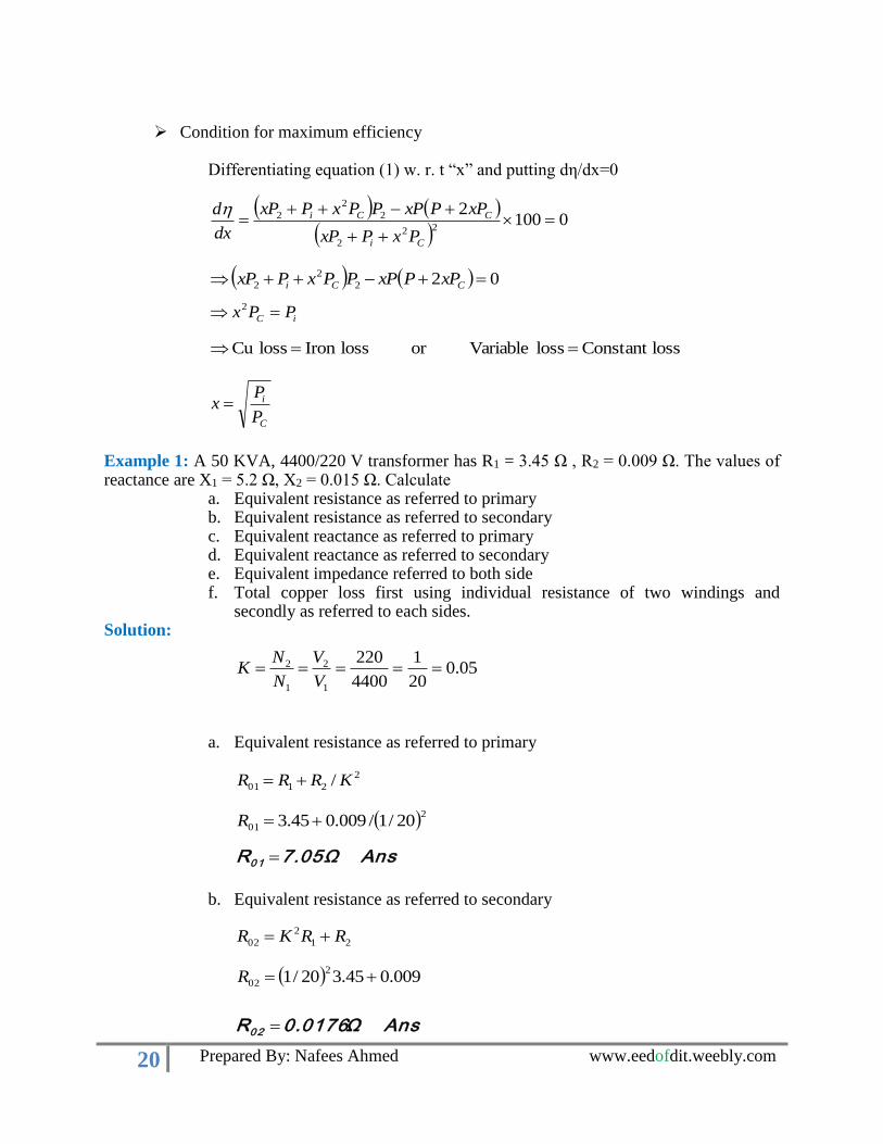
Condition for maximum efficiency
Differentiating equation (1) w. r. t “x” and putting dη/dx=0
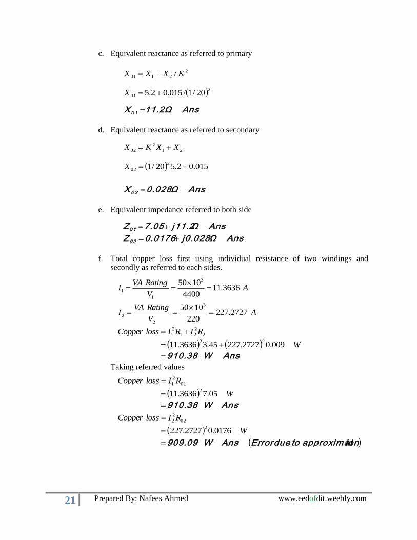
Example 1: A 50 KVA, 4400/220 V transformer has R1 = 3.45 Ω , R2 = 0.009 Ω. The values of reactance are X1 = 5.2 Ω, X2 = 0.015 Ω. Calculate
a. Equivalent resistance as referred to primary b. Equivalent resistance as referred to secondary c. Equivalent reactance as referred to primary d. Equivalent reactance as referred to secondary e. Equivalent impedance referred to both side f. Total copper loss first using individual resistance of two windings and
secondly as referred to each sides. Solution:
a. Equivalent resistance as referred to primary
b. Equivalent resistance as referred to secondary
0100
222
2
2
2
2
Ci
CCi
PxPxP
xPPxPPPxPxP
dx
d
022
2
2 CCi xPPxPPPxPxP
iC PPx 2
C
i
P
Px
lossConstantlossVariableorlossIronlossCu
05.020
1
4400
220
1
2
1
2 V
V
N
NK
2
2101 / KRRR
201 20/1/009.045.3 R
AnsΩ7.05R01
21
2
02 RRKR
009.045.320/12
02 R
AnsΩ0.0176R02
21 Prepared By: Nafees Ahmed www.eedofdit.weebly.com
c. Equivalent reactance as referred to primary
d. Equivalent reactance as referred to secondary
e. Equivalent impedance referred to both side
f. Total copper loss first using individual resistance of two windings and
secondly as referred to each sides.
Taking referred values
2
2101 / KXXX
201 20/1/015.02.5 X
AnsΩ11.2X 01
21
2
02 XXKX
015.02.520/12
02 X
AnsΩ0.028X 02
Ansj11.2Ω7.05Z01
AnsΩ j0.0280.0176Z02
2
2
21
2
1 RIRIlossCopper
AV
RatingVAI 3636.11
4400
1050 3
1
1
AV
RatingVAI 2727.227
220
1050 3
2
2
W009.02727.22745.33636.1122
AnsW910.38
01
2
1 RIlossCopper
W05.73636.112
AnsW910.38
02
2
2 RIlossCopper
W0176.02727.2272
ionapproximattodue ErrorAnsW909.09

22 Prepared By: Nafees Ahmed www.eedofdit.weebly.com
AI 09.911000
10001001
Example 1: Following results were obtained on a 100 KVA, 11000/220 V, single phase transformer
(i) OC Test (LV Side) 220 V, 45 A, 2 KW (ii) SC Test (HV Side) 500 V, 9.09 A, 3 KW
Determine equivalent circuit parameter of transformer referred to low voltage side and efficiency at full load unity power factor. Solution: Equivalent circuit parameters:
From OC test: Pi = P0 = 2 KW, I0 = 45 A, V2 = 220 V
P0 = Pi = V2I0Cosϕ0
Ie = I0Cosϕ0=9.09 A Im = I0Sinϕ0=44.07 A
From SC test: PC = Wsc = 3 KW, Isc = 9.09 A, Vsc = 500 V
Efficiency at full load and unity power factor:
Note:
Full load HV side current Here SC Test is done on full load, so 3 KW is the full load cu loss.
202.002
0 IV
PCos i
AnsΩ24.20I
VR
e
20 AnsΩ5
I
VX&
m
20
01
2 RIW scsc
01ZIV scsc
AnsΩ36.31R01
AnsΩ55Z 01
2
01
2
0101 RZX
AnsΩ41.31X 01
1002
2
2
Ci PxPCosRatedVAx
CosRatedVAx
10031211001
110012
Ans95.24%η