Embed Size (px)
Citation preview

8Semiconductor Crystals
BAND GAP 187
EQUATIONS OF MOTION 191Physical derivation of 193Holes 194Effective mass 197Physical interpretation of the effective mass 198Effective masses in semiconductors 200Silicon and germanium 202
INTRINSIC CARRIER CONCENTRATION 205Intrinsic mobility 208
IMPURITY CONDUCTIVITY 209Donor states 209Acceptor states 211Thermal ionization of donors and acceptors 213
THERMOELECTRIC EFFECTS 214
SEMIMETALS 215
SUPERLATTICES 216Bloch oscillator 217Zener tunneling 217
SUMMARY 217
PROBLEMS 218
1. Impurity orbits 2182. Ionization of donors 218
NOTE: The discussion of carrier orbits in applied fields is continued in Chapter 9.
�k � F
ch08.qxd 8/13/04 4:23 PM Page 185

186
1023
1022
1021
1020
1019
1018
1017
1016
1015
1014
1013
Cu
NaK
Semimetals
Metals
Graphite
As
Sb
Bi
Semiconductors (at room temperature)
(pure)Ge
Con
duct
ion
elec
tron
con
cent
ratio
n, c
m–3
Figure 1 Carrier concentrations for metals, semimetals, and semiconductors. The semiconductorrange may be extended upward by increasing the impurity concentration, and the range can be ex-tended downward to merge eventually with the insulator range.
3. Hall effect with two carrier types 2184. Cyclotron resonance for a spheroidal
energy surface 2195. Magnetoresistance with two carrier types 219
ch08.qxd 8/13/04 4:23 PM Page 186

chapter 8: semiconductor crystals
Carrier concentrations representative of metals, semimetals, and semicon-ductors are shown in Fig. 1. Semiconductors are generally classified by theirelectrical resistivity at room temperature, with values in the range of 10�2 to109 ohm-cm, and strongly dependent on temperature. At absolute zero a pure,perfect crystal of most semiconductors will be an insulator, if we arbitrarily de-fine an insulator as having a resistivity above 1014 ohm-cm.
Devices based on semiconductors include transistors, switches, diodes,photovoltaic cells, detectors, and thermistors. These may be used as singlecircuit elements or as components of integrated circuits. We discuss in thischapter the central physical features of the classical semiconductor crystals,particularly silicon, germanium, and gallium arsenide.
Some useful nomenclature: the semiconductor compounds of chemicalformula AB, where A is a trivalent element and B is a pentavalent element, arecalled III-V (three-five) compounds. Examples are indium antimonide andgallium arsenide. Where A is divalent and B is hexavalent, the compound iscalled a II-VI compound; examples are zinc sulfide and cadmium sulfide. Siliconand germanium are sometimes called diamond-type semiconductors, becausethey have the crystal structure of diamond. Diamond itself is more an insulatorrather than a semiconductor. Silicon carbide SiC is a IV-IV compound.
A highly purified semiconductor exhibits intrinsic conductivity, as distin-guished from the impurity conductivity of less pure specimens. In the intrin-sic temperature range the electrical properties of a semiconductor are notessentially modified by impurities in the crystal. An electronic band schemeleading to intrinsic conductivity is indicated in Fig. 2. The conduction band isvacant at absolute zero and is separated by an energy gap Eg from the filledvalence band.
The band gap is the difference in energy between the lowest point of theconduction band and the highest point of the valence band. The lowest pointin the conduction band is called the conduction band edge; the highestpoint in the valence band is called the valence band edge.
As the temperature is increased, electrons are thermally excited from thevalence band to the conduction band (Fig. 3). Both the electrons in the con-duction band and the vacant orbitals or holes left behind in the valence bandcontribute to the electrical conductivity.
BAND GAP
The intrinsic conductivity and intrinsic carrier concentrations are largelycontrolled by Eg/kBT, the ratio of the band gap to the temperature. When thisratio is large, the concentration of intrinsic carriers will be low and the
187
ch08.qxd 8/13/04 4:23 PM Page 187

188
EgEne
rgy
Vacant conduction band
Forbidden band
Filled valence band
Figure 2 Band scheme for intrinsic conductivity in a semiconductor. At 0 K the conductivity iszero because all states in the valence band are filled and all states in the conduction band are va-cant. As the temperature is increased, electrons are thermally excited from the valence band to theconduction band, where they become mobile. Such carriers are called “intrinsic.”
109
1010
1011
1012
1013
1014
200 215 230 245Temperature, K
(a)
260 275 290 305
Ge
Ele
ctro
n co
ncen
trat
ion
in c
arri
ers
per
cm3
109
1010
1011
1012
1013
1014
275 300 325 350Temperature, K
(b)
375 400 425 450
Si
Ele
ctro
n co
ncen
trat
ion
in c
arri
ers
per
cm3
Figure 3 Intrinsic electron concentration as a function of temperature for (a) germanium and (b) silicon. Under intrinsic conditions the hole concentration is equal to the electron concentra-tion. The intrinsic concentration at a given temperature is higher in Ge than in Si because theenergy gap is narrower in Ge (0.66 eV) than in Si (1.11 eV). (After W. C. Dunlap.)
conductivity will be low. Band gaps of representative semiconductors are givenin Table 1. The best values of the band gap are obtained by optical absorption.
In a direct absorption process the threshold of continuous optical ab-sorption at frequency �g measures the band gap as shown in Figs. 4aand 5a. A photon is absorbed by the crystal with the creation of an electronand a hole.
In the indirect absorption process in Figs. 4b and 5b the minimumenergy gap of the band structure involves electrons and holes separated by a
Eg � ��g
ch08.qxd 8/13/04 4:23 PM Page 188

8 Semiconductor Crystals 189
Absorption
CRYSTAL WITH DIRECT GAP CRYSTAL WITH INDIRECT GAP
Photon energy ��
Transparentregion
Onset of directphoton
transition
��g
(a)
Absorption
Photon energy ��
(b)
Onset of indirectphoton transition
Eg + �� Evert
Onset of directtransition
Figure 4 Optical absorption in pure insulators at absolute zero. In (a) the threshold determinesthe energy gap as In (b) the optical absorption is weaker near the threshold: at
a photon is absorbed with the creation of three particles: a free electron, a freehole, and a phonon of energy . In (b) the energy Evert marks the threshold for the creation of afree electron and a free hole, with no phonon involved. Such a transition is called vertical; it issimilar to the direct transition in (a). These plots do not show absorption lines that sometimes areseen lying just to the low energy side of the threshold. Such lines are due to the creation of abound electron-hole pair, called an exciton.
��
�� � Eg � ��
Eg � ��g.
��
Conductionband edge
Conductionband edge
Valence band edgeValence band edge
0(b)
0(a)
–kc kckk
���g
Figure 5 In (a) the lowest point of the conduction band occurs at the same value of k as the highestpoint of the valence band. A direct optical transition is drawn vertically with no significant change ofk, because the absorbed photon has a very small wavevector. The threshold frequency �g for absorp-tion by the direct transition determines the energy gap The indirect transition in (b) in-volves both a photon and a phonon because the band edges of the conduction and valence bands arewidely separated in k space. The threshold energy for the indirect process in (b) is greater than thetrue band gap. The absorption threshold for the indirect transition between the band edges is at
, where � is the frequency of an emitted phonon of wavevector K � �kg. At highertemperatures phonons are already present; if a phonon is absorbed along with a photon, the thresh-old energy is . Note: The figure shows only the threshold transitions. Transitions occurgenerally between almost all points of the two bands for which the wavevectors and energy can beconserved.
�� � Eg � ��
�� � Eg � ��
Eg � ��g.
ch08.qxd 8/13/04 4:23 PM Page 189
190
substantial wavevector kc. Here a direct photon transition at the energy of theminimum gap cannot satisfy the requirement of conservation of wavevector,because photon wavevectors are negligible at the energy range of interest. Butif a phonon of wavevector K and frequency � is created in the process, thenwe can have
as required by the conservation laws. The phonon energy will generally bemuch less than Eg: a phonon even of high wavevector is an easily accessiblesource of crystal momentum because the phonon energies are characteristi-cally small (�0.01 to 0.03 eV) in comparison with the energy gap. If the tem-perature is high enough that the necessary phonon is already thermally excitedin the crystal, it is possible also to have a photon absorption process in whichthe phonon is absorbed.
The band gap may also be deduced from the temperature dependenceof the conductivity or of the carrier concentration in the intrinsic range. Thecarrier concentration is obtained from measurements of the Hall voltage(Chapter 6), sometimes supplemented by conductivity measurements. Opticalmeasurements determine whether the gap is direct or indirect. The bandedges in Ge and in Si are connected by indirect transitions; the band edges inInSb and GaAs are connected by a direct transition (Fig. 6). The gap in �Sn is
��
k(photon) � kc � K � 0 ; �� � Eg � �� ,
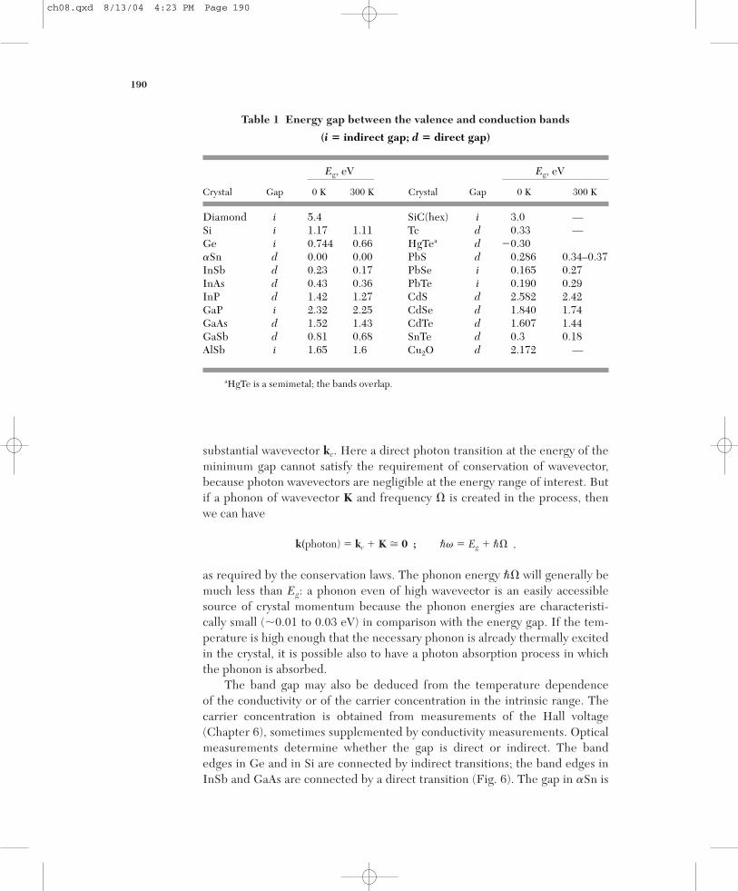
Table 1 Energy gap between the valence and conduction bands
(i � indirect gap; d � direct gap)
Eg, eV Eg, eV
Crystal Gap 0 K 300 K Crystal Gap 0 K 300 K
Diamond i 5.4 SiC(hex) i 3.0 —Si i 1.17 1.11 Tc d 0.33 —Ge i 0.744 0.66 HgTea d �0.30�Sn d 0.00 0.00 PbS d 0.286 0.34–0.37InSb d 0.23 0.17 PbSe i 0.165 0.27InAs d 0.43 0.36 PbTe i 0.190 0.29InP d 1.42 1.27 CdS d 2.582 2.42GaP i 2.32 2.25 CdSe d 1.840 1.74GaAs d 1.52 1.43 CdTe d 1.607 1.44GaSb d 0.81 0.68 SnTe d 0.3 0.18AlSb i 1.65 1.6 Cu2O d 2.172 —
aHgTe is a semimetal; the bands overlap.
ch08.qxd 8/13/04 4:23 PM Page 190

8 Semiconductor Crystals 191
direct and is exactly zero; HgTe and HgSe are semimetals and have negativegaps—the conduction and valence bands overlap.
EQUATIONS OF MOTION
We derive the equation of motion of an electron in an energy band. Welook at the motion of a wave packet in an applied electric field. Suppose thatthe wave packet is made up of wavefunctions assembled near a particularwavevector k. The group velocity by definition is vg � d�/dk. The frequency as-sociated with a wavefunction of energy � by quantum theory is , and so
(1)
The effects of the crystal on the electron motion are contained in the disper-sion relation �(k).
vg � ��1 d�/dk or v � ��1 �k�(k) .
� � �/�
10
1
102
103
104
105
0.1 0.3 0.5 0.7
Abs
orpt
ion
coef
ficie
nt in
cm
–1
�� in eV
Figure 6 Optical absorption in pure indium antimonide, InSb. The transition is direct becauseboth conduction and valence band edges are at the center of the Brillouin zone, k � 0. Notice thesharp threshold. (After G. W. Gobeli and H. Y. Fan.)
ch08.qxd 8/13/04 4:23 PM Page 191

The work �� done on the electron by the electric field E in the timeinterval �t is
(2)
We observe that
(3)
using (1). On comparing (2) with (3) we have
(4)
whence We may write (4) in terms of the external force F as
(5)
This is an important relation: in a crystal is equal to the external forceon the electron. In free space d(mv)/dt is equal to the force. We have not over-thrown Newton’s second law of motion: the electron in the crystal is subject toforces from the crystal lattice as well as from external sources.
The force term in (5) also includes the electric field and the Lorentz forceon an electron in a magnetic field, under ordinary conditions where the mag-netic field is not so strong that it breaks down the band structure. Thus theequation of motion of an electron of group velocity v in a constant magneticfield B is
(CGS) (6)
where the right-hand side of each equation is the Lorentz force on the electron.With the group velocity the rate of change of the wavevector is
(CGS) (7)
where now both sides of the equation refer to the coordinates in k space.We see from the vector cross-product in (7) that in a magnetic field
an electron moves in k space in a direction normal to the direction of the gra-dient of the energy �, so that the electron moves on a surface of constantenergy. The value of the projection kB of k on B is constant during themotion. The motion in k space is on a plane normal to the direction of B, andthe orbit is defined by the intersection of this plane with a surface of constantenergy.
(SI) dkdt
� � e�2 �k� Bdk
dt � � e
�2c �k� B ;
v � ��1gradk�,
(SI) �dkdt
� �ev B�dkdt
� �ecv B ;
�dk/dt
�dkdt
� F .
�dk/dt � �eE.
�k � �(eE/�)�t ,
�� � (d�/dk)�k � �vg �k ,
�� � �eEvg �t .
192
ch08.qxd 8/13/04 4:23 PM Page 192
Physical Derivation of
We consider the Bloch eigenfunction �k belonging to the energy eigen-value �k and wavevector k:
(8)
The expectation value of the momentum of an electron in the Bloch state k is
(9)
using We examine the transfer of momentum between the electron and the lat-
tice when the state k of the electron is changed to k � k by the applicationof an external force. We imagine an insulating crystal electrostatically neutralexcept for a single electron in the state k of an otherwise empty band.
We suppose that a weak external force is applied for a time interval suchthat the total impulse given to the entire crystal system is J � �F dt. If theconduction electron were free (m* � m), the total momentum imparted tothe crystal system by the impulse would appear in the change of momentum ofthe conduction electron:
(10)
The neutral crystal suffers no net interaction with the electric field, either directly or indirectly through the free electron.
If the conduction electron interacts with the periodic potential of the crys-tal lattice, we must have
(11)
From the result (9) for pel we have
(12)
The change plat in the lattice momentum resulting from the change ofstate of the electron may be derived by an elementary physical consideration.An electron reflected by the lattice transfers momentum to the lattice. If anincident electron with plane wave component of momentum is reflectedwith momentum the lattice acquires the momentum as re-quired by momentum conservation. The momentum transfer to the latticewhen the state �k goes over to �k�k is
(13)plat � ���G
G[(�k �C(k � G) �2 � k] ,
��G,�(k � G),�k
pel � �k � �G
�G[(�k �C(k � G) �2) � k] .
J � ptot � plat � pel .
J � ptot � pel � �k .
� �C(k � G) �2 � 1.
Pel � (k ��i�� �k) � �G
�(k � G) �C(k � G) �2 � �(k � �G
G �C(k � G) �2) ,
�k � �G
C(k � G) exp[i(k � G) � r] .
�k̇ � F
8 Semiconductor Crystals 193
ch08.qxd 8/13/04 4:23 PM Page 193

because the portion
(14)
of each individual component of the initial state is reflected during the statechange k.
The total momentum change is therefore
(15)
exactly as for free electrons, Eq. (10). Thus from the definition of J, we have
(16)
derived in (5) by a different method. A rigorous derivation of (16) by an en-tirely different method is given in Appendix E.
Holes
The properties of vacant orbitals in an otherwise filled band are importantin semiconductor physics and in solid state electronics. Vacant orbitals in aband are commonly called holes, and without holes there would be no transis-tors. A hole acts in applied electric and magnetic fields as if it has a positivecharge �e. The reason is given in five steps in the boxes that follow.
�dk /dt � F ,
pel � plat � J � �k ,
�k �C(k � G) �2 � k
194
1. (17)
The total wavevector of the electrons in a filled band is zero: �k � 0,where the sum is over all states in a Brillouin zone. This result followsfrom the geometrical symmetry of the Brillouin zone: every fundamentallattice type has symmetry under the inversion operation r→ �r aboutany lattice point; it follows that the Brillouin zone of the lattice also hasinversion symmetry. If the band is filled all pairs of orbitals k and �k arefilled, and the total wavevector is zero.
If an electron is missing from an orbital of wavevector ke, the totalwavevector of the system is �ke and is attributed to the hole. This resultis surprising: the electron is missing from ke and the position of the holeis usually indicated graphically as situated at ke, as in Fig. 7. But the truewavevector kh of the hole is �ke, which is the wavevector of the point Gif the hole is at E. The wavevector �ke enters into selection rules forphoton absorption.
The hole is an alternate description of a band with one missing elec-tron, and we either say that the hole has wavevector �ke or that the bandwith one missing electron has total wavevector �ke.
kh � �ke .
ch08.qxd 8/13/04 4:23 PM Page 194

8 Semiconductor Crystals 195
2. (18)
Here the zero of energy of the valence band is at the top of the band.The lower in the band the missing electron lies, the higher the energy ofthe system. The energy of the hole is opposite in sign to the energy ofthe missing electron, because it takes more work to remove an electronfrom a low orbital than from a high orbital. Thus if the band is symmet-ric,1 �e(ke) � �e(�ke) � ��h(�ke)� ��h(kh). We construct in Fig. 8 aband scheme to represent the properties of a hole. This hole band is ahelpful representation because it appears right side up.
3. (19)
The velocity of the hole is equal to the velocity of the missing electron.From Fig. 8 we see that so that vh(kh) � ve(k e).��h(kh) � ��e(ke),
vh � ve .
�h(kh) � ��e(k e) .
�
khke
kGE
Q
Valence band
Electron removed
Conduction band
��
Figure 7 Absorption of a photon of energy and negligible wavevector takes an electron fromE in the filled valence band to Q in the conduction band. If ke was the wavevector of the electronat E, it becomes the wavevector of the electron at Q. The total wavevector of the valence bandafter the absorption is �ke, and this is the wavevector we must ascribe to the hole if we describethe valence band as occupied by one hole. Thus kh � �ke; the wavevector of the hole is the sameas the wavevector of the electron which remains at G. For the entire system the total wavevectorafter the absorption of the photon is ke � kh � 0, so that the total wavevector is unchanged by theabsorption of the photon and the creation of a free electron and free hole.
��
1Bands are always symmetric under the inversion k → �k if the spin-orbit interaction isneglected. Even with spin-orbit interaction, bands are always symmetric if the crystal structurepermits the inversion operation. Without a center of symmetry, but with spin-orbit interaction, thebands are symmetric if we compare subbands for which the spin direction is reversed: �(k, ↑) �
�(�k, ↓). See QTS, Chapter 9.
ch08.qxd 8/13/04 4:23 PM Page 195

196
4. (20)
We show below that the effective mass is inversely proportional to thecurvature d2�/dk2, and for the hole band this has the opposite sign to thatfor an electron in the valence band. Near the top of the valence band me
is negative, so that mh is positive.
5. (21)
This comes from the equation of motion
(CGS) (22)
that applies to the missing electron when we substitute �kh for ke and vh
for ve. The equation of motion for a hole is that of a particle ofpositive charge e. The positive charge is consistent with the electriccurrent carried by the valence band of Fig. 9: the current is carried bythe unpaired electron in the orbital G:
(23)
which is just the current of a positive charge moving with the velocity as-cribed to the missing electron at E. The current is shown in Fig. 10.
j � (�e)v(G) �(�e)[�v(E)] � ev(E) ,
�dke
dt � �e(E �1
cve B)
� dkh
dt � e(E � 1c vh B) .
mh � �me .
�
kh
ke
k
Hole band constructedwith kh = –ke and�h(kh) = –�e(ke), tosimulate dynamics
of a hole.
Valence bandwith one
electron missing
Figure 8 The upper half of the figure shows the hole band that simulates the dynamics of a hole,constructed by inversion of the valence band in the origin. The wavevector and energy of the holeare equal, but opposite in sign, to the wavevector and energy of the empty electron orbital in the va-lence band. We do not show the disposition of the electron removed from the valence band at ke.
ch08.qxd 8/13/04 4:23 PM Page 196

8 Semiconductor Crystals 197
Effective Mass
When we look at the energy-wavevector relation for freeelectrons, we see that the coefficient of k2 determines the curvature of � versusk. Turned about, we can say that 1/m, the reciprocal mass, determines the cur-vature. For electrons in a band there can be regions of unusually high curva-ture near the band gap at the zone boundary, as we see from the solutions inChapter 7 of the wave equation near the zone boundary. If the energy gap issmall in comparison with the free electron energy � at the boundary, the cur-vature is enhanced by the factor �/Eg.
In semiconductors the band width, which is like the free electron energy,is of the order of 20 eV, while the band gap is of the order of 0.2 to 2 eV. Thusthe reciprocal mass is enhanced by a factor 10 to 100, and the effective mass isreduced to 0.1–0.01 of the free electron mass. These values apply near theband gap; as we go away from the gap the curvatures and the masses are likelyto approach those of free electrons.
To summarize the solutions of Chapter 7 for U positive, an electron nearthe lower edge of the second band has an energy that may be written as
(24)�(K) � �c � (�2/2me)K2 ; me
/m � 1 /[(2�/U)�1] .
� � (�2/2m)k2
Ex
kx
�
AB
CD
E
F
GH
IJ
K
(b)
Ex
kx
�
AB
CD
E
F
GH
IJK
(c)
kx
�
AB
CD E
F
GH I
JK
(a)
Figure 9 (a) At t � 0 all states are filled except F at the top of the band; the velocity vx is zero at Fbecause d�/dkx � 0. (b) An electric field Ex is applied in the �x direction. The force on the elec-trons is in the �kx direction and all electrons make transitions together in the �kx direction, mov-ing the hole to the state E. (c) After a further interval the electrons move farther along in k spaceand the hole is now at D.
E
ve
vh
je
jh
e
hFigure 10 Motion of electrons in the conduction band andholes in the valence band in the electric field E. The holeand electron drift velocities are in opposite directions, but theirelectric currents are in the same direction, the direction of theelectric field.
ch08.qxd 8/13/04 4:23 PM Page 197
Here K is the wavevector measured from the zone boundary, and me denotesthe effective mass of the electron near the edge of the second band. An elec-tron near the top of the first band has the energy
(25)
The curvature and hence the mass will be negative near the top of the firstband, but we have introduced a minus sign into (25) in order that the symbolmh for the hole mass will have a positive value—see (20) above.
The crystal does not weigh any less if the effective mass of a carrier is lessthan the free electron mass, nor is Newton’s second law violated for the crystaltaken as a whole, ions plus carriers. The important point is that an electron in aperiodic potential is accelerated relative to the lattice in an applied electric ormagnetic field as if the mass of the electron were equal to an effective masswhich we now define.
We differentiate the result (1) for the group velocity to obtain
. (26)
We know from (5) that whence
(27)
If we identify as a mass, then (27) assumes the form of Newton’ssecond law. We define the effective mass m* by
(28)
It is easy to generalize this to take account of an anisotropic electron en-ergy surface, as for electrons in Si or Ge. We introduce the components of thereciprocal effective mass tensor
(29)
where �, are Cartesian coordinates.
Physical Interpretation of the Effective Mass
How can an electron of mass m when put into a crystal respond to appliedfields as if the mass were m*? It is helpful to think of the process of Bragg re-flection of electron waves in a lattice. Consider the weak interaction approxi-mation treated in Chapter 7. Near the bottom of the lower band the orbital isrepresented quite adequately by a plane wave exp(ikx) with momentum the wave component exp[i(k � G)x] with momentum is small and�(k�G)
�k;
� 1m*
���
1�2
d2 �k
dk� dk�
; dv�
dt � � 1
m*��
F� ,
1m*
�
1�2
d2�
dk2 .
�2/(d2�/dk2)
dvg
dt � � 1
�2
d2�
dk2 F ; or F �
�2
d2��dk2
dvg
dt .
dk/dt � F��,
dvg
dt � ��1
d2�dk dt
� ��1 �d2�
dk2
dkdt
�(K) � �v
�
(�2/2mh)K2 ; mh/m � 1/[(2 �/U) � 1] .
198
ch08.qxd 8/13/04 4:23 PM Page 198

8 Semiconductor Crystals 199
increases only slowly as k is increased, and in this region m* m. An increasein the reflected component exp[i(k � G)x] as k is increased represents mo-mentum transfer to the electron from the lattice.
Near the boundary the reflected component is quite large; at the bound-ary it becomes equal in amplitude to the forward component, at which pointthe eigenfunctions are standing waves, rather than running waves. Here themomentum component cancels the momentum component
A single electron in an energy band may have positive or negative effectivemass: the states of positive effective mass occur near the bottom of a band be-cause positive effective mass means that the band has upward curvature(d2�/dk2 is positive). States of negative effective mass occur near the top of theband. A negative effective mass means that on going from state k to state k � k, the momentum transfer to the lattice from the electron is larger than the momentum transfer from the applied force to the electron. Although k isincreased by k by the applied electric field, the approach to Bragg reflectioncan give an overall decrease in the forward momentum of the electron; whenthis happens the effective mass is negative (Fig. 11).
As we proceed in the second band away from the boundary, the amplitudeof exp[i(k � G)x] decreases rapidly and m* assumes a small positive value.Here the increase in electron velocity resulting from a given external impulseis larger than that which a free electron would experience. The lattice makesup the difference through the reduced recoil it experiences when the ampli-tude of exp[i(k � G)x] is diminished.
If the energy in a band depends only slightly on k, then the effective masswill be very large. That is, m*/m � 1 when d2�/dk2 is very small. The tight-binding approximation discussed in Chapter 9 gives quick insight into the for-mation of narrow bands. If the wavefunctions centered on neighboring atomsoverlap very little, then the overlap integral is small; the width of the band
�(12 G).�(�
12 G)
(a) (b)
V = 0 V
GridCrystal
Incident electronbeam
BeamBragg-reflected
Figure 11 Explanation of negative effective masses which occur near, but below, a Brillouin zoneboundary. In (a) the energy of the electron beam incident on a thin crystal is slightly too low to sat-isfy the condition for Bragg reflection and the beam is transmitted through the crystal. The appli-cation of a small voltage across the grid may, as in (b), cause the Bragg condition to be satisfied,and the electron beam will then be reflected from the appropriate set of crystal planes.
ch08.qxd 8/13/04 4:23 PM Page 199

200
narrow, and the effective mass large. The overlap of wavefunctions centeredon neighboring atoms is small for the inner or core electrons. The 4f electronsof the rare earth metals, for example, overlap very little.
Effective Masses in Semiconductors
In many semiconductors it has been possible to determine by cyclotronresonance the effective masses of carriers in the conduction and valence bandsnear the band edges. The determination of the energy surface is equivalent toa determination of the effective mass tensor (29). Cyclotron resonance in asemiconductor is carried out with centimeter wave or millimeter wave radia-tion at low carrier concentration.
The current carriers are accelerated in helical orbits about the axis of astatic magnetic field. The angular rotation frequency �c is
(30)
where m* is the appropriate cyclotron effective mass. Resonant absorption ofenergy from an rf electric field perpendicular to the static magnetic field (Fig. 12) occurs when the rf frequency is equal to the cyclotron frequency.Holes and electrons rotate in opposite senses in a magnetic field.
We consider the experiment for m*/m � 0.1. At fc � 24 GHz, or �c �
1.5 1011 s�1, we have B � 860 G at resonance. The line width is determinedby the collision relaxation time , and to obtain a distinctive resonance it isnecessary that �c 1. The mean free path must be long enough to permit theaverage carrier to get one radian around a circle between collisions. The re-quirements are met with the use of higher frequency radiation and highermagnetic fields, with high purity crystals in liquid helium.
In direct-gap semiconductors with band edges at the center of the Bril-louin zone, the bands have the structure shown in Fig. 13. The conductionband edge is spherical with the effective mass m0:
(31)�c � Eg � �2k2/2m e ,
(SI) �c �
eBm*(CGS) �c �
eBm*c ,
Orbit of electron
B (static)
ErfFigure 12 Arrangement of fields in a cyclotron resonance experiment in a semiconductor. The sense of the circulation is opposite for electronsand holes.
ch08.qxd 8/13/04 4:23 PM Page 200

8 Semiconductor Crystals 201
referred to the valence band edge. The valence bands are characteristicallythreefold near the edge, with the heavy hole hh and light hole lh bands degen-erate at the center, and a band soh split off by the spin-orbit splitting :
(32).
Values of the mass parameters are given in Table 2. The forms (32) are onlyapproximate, because even close to k � 0 the heavy and light hole bands arenot spherical—see the discussion below for Ge and Si.
The perturbation theory of band edges (Problem 9.8) suggests that theelectron effective mass should be proportional to the band gap, approximately,
�v(soh) � � � �2k2/2msoh
�v(hh) � ��2k2/2mhh ; �v(lh) � ��2k2/2mlh ;
�
Eg
Electrons
Heavy holes
k
Light holes
Split-off holes Figure 13 Simplified view of theband edge structure of a direct-gapsemiconductor.
Table 2 Effective masses of electrons and holes in direct-gap semiconductors
Electron Heavy hole Light hole Split-off hole Spin-orbit Crystal me/m mhh/m mlh/m msoh/m , eV
InSb 0.015 0.39 0.021 (0.11) 0.82InAs 0.026 0.41 0.025 0.08 0.43InP 0.073 0.4 (0.078) (0.15) 0.11GaSb 0.047 0.3 0.06 (0.14) 0.80GaAs 0.066 0.5 0.082 0.17 0.34Cu2O 0.99 — 0.58 0.69 0.13
ch08.qxd 8/13/04 4:23 PM Page 201
202
for a direct gap crystal. We use Tables 1 and 2 to find the fairly constant valuesme/(mEg) � 0.063, 0.060, and 0.051 in (eV)�1 for the series InSb, InAs, andInP, in agreement with this suggestion.
Silicon and Germanium
The conduction and valence bands of germanium are shown in Fig. 14,based on a combination of theoretical and experimental results. The valenceband edge in both Si and Ge is at k � 0 and is derived from p3/2 and p1/2 statesof the free atoms, as is clear from the tight-binding approximation (Chapter 9)to the wavefunctions.
The p3/2 level is fourfold degenerate as in the atom; the four states corre-spond to mJ values and The p1/2 level is doubly degenerate, with
The p3/2 states are higher in energy than the p1/2 states; the energydifference is a measure of the spin-orbit interaction.
The valence band edges are not simple. Holes near the band edge arecharacterized by two effective masses, light and heavy. These arise from thetwo bands formed from the p3/2 level of the atom. There is also a band formedfrom the p1/2 level, split off from the p3/2 level by the spin-orbit interaction.The energy surfaces are not spherical, but warped (QTS, p. 271):
(33)
The choice of sign distinguishes the two masses. The split-off band has �(k) � � � Ak2. The experiments give, in units
Si: A � �4.29 ; |B| � 0.68 ; |C| � 4.87 ; � 0.044 eVGe: A � �13.38 ; |B| � 8.48 ; |C| � 13.15 ; � 0.29 eV
Roughly, the light and heavy holes in germanium have masses 0.043 m and0.34 m; in silicon 0.16 m and 0.52 m; in diamond 0.7 m and 2.12 m.
The conduction band edges in Ge are at the equivalent points L of theBrillouin zone, Fig. 15a. Each band edge has a spheroidal energy surface ori-ented along a �111� crystal axis, with a longitudinal mass ml � 1.59 m and atransverse mass mt � 0.082 m. For a static magnetic field at an angle � withthe longitudinal axis of a spheroid, the effective cyclotron mass mc is
(34)
Results for Ge are shown in Fig. 16.In silicon the conduction band edges are spheroids oriented along the
equivalent �100� directions in the Brillouin zone, with mass parameters ml � 0.92 m and mt � 0.19 m, as in Fig. 17a. The band edges lie along the lineslabeled in the zone of Fig. 15a, a little way in from the boundary points X.
In GaAs we have A � �6.98, B � �4.5, |C| � 6.2, � 0.341 eV. Theband structure is shown in Fig. 17b. It has a direct band gap with an isotropicconduction electron mass of 0.067 m.
1mc
2 �
cos2�
mt2 �
sin2�mtml
�2/2m,
�(k) � Ak2 � [B2k4 � C2(kx
2ky2 � ky
2kz2 � kz
2kx2)]1/2
mJ � �
12.
�
12.�
32
ch08.qxd 8/13/04 4:23 PM Page 202

8 Semiconductor Crystals 203
–13
–12
–11
–10
–9
–8
–6
–5
–4
–3
–2
–1
0
1
2
3
4
5
6
–7
k = ( )a2� k = a
2�12
12
12 [111] [100]
k = 0 (1 0 0)
5.4 eV
2.0 eV
3.5 eV
0.36 eV
1.1 eV
0.29 eV
1.01 eV
3.8 eV
Eg = 0.9 eV
GeE
nerg
y in
eV
Figure 14 Calculated band structure of germanium, after C. Y. Fong. The general features are ingood agreement with experiment. The four valence bands are shown in gray. The fine structure ofthe valence band edge is caused by spin-orbit splitting. The energy gap is indirect; the conductionband edge is at the point The constant energy surfaces around this point are ellipsoidal.(2��a)(1
2 12 12).
ch08.qxd 8/13/04 4:23 PM Page 203

204
X
W
kz
kz
ky ky
kx
kxK
UL
��
��
��
fcc
(a) (b)
Hbcc
P
D
NG
Figure 15 Standard labels of the symmetry points and axes of the Brillouin zones of the fcc andbcc lattices. The zone centers are �. In (a) the boundary point at (2�/a)(100) is X; the boundarypoint at is L; the line runs between � and X. In (b) the corresponding symbols areH, P, and .
(2�/a)(12 12 12)
0
0.04
0.08
0.12
0.16
0.20
0.24
0.28
0.32
0.36
0.40
0–10 10 20 30 40 50 60 70 80 90 100Angle in degrees in (110) plane from [001] axis
[001
]
[111
]
[110
]
Eff
ectiv
e m
ass,
mc/
m
Figure 16 Effective cyclotron mass of electrons in germa-nium at 4 K for magnetic field directions in a (110) plane.There are four independent mass spheroids in Ge, onealong each [111] axis, but viewed in the (110) plane twospheroids always appear equivalent. (After Dresselhaus,Kip, and Kittel.)
ch08.qxd 8/13/04 4:23 PM Page 204

INTRINSIC CARRIER CONCENTRATION
We want the concentration of intrinsic carriers as a function of tempera-ture, in terms of the band gap. We do the calculation for simple parabolic bandedges. We first calculate in terms of the chemical potential � the number ofelectrons excited to the conduction band at temperature T. In semiconductorphysics � is called the Fermi level. At the temperatures of interest we maysuppose for the conduction band of a semiconductor that � � � � kBT, so thatthe Fermi-Dirac distribution function reduces to
(35)
This is the probability that a conduction electron orbital is occupied, in an approximation valid when fe � 1.
The energy of an electron in the conduction band is
(36)
where Ec is the energy at the conduction band edge, as in Fig. 18. Here me is the effective mass of an electron. Thus from (6.20) the density of states at � is
(37)De(�) �
12�2�
2me
�2 3/2
(� � Ec)1/2 .
�k � Ec � �2k2/2me ,
fe exp[(���)/kBT] .
8 Semiconductor Crystals 205
–4
–3
–2
–1
0
Ene
rgy
in e
V 1
2
3
4
L �
(b)(a)X
kx
ky
kz
Figure 17a Constant energy ellipsoids forelectrons in silicon, drawn for ml/mt � 5.
Figure 17b Band structure of GaAs, after S. G. Louie.
ch08.qxd 8/13/04 4:23 PM Page 205

The concentration of electrons in the conduction band is
(38)
which integrates to give
(39)
The problem is solved for n when � is known. It is useful to calculate theequilibrium concentration of holes p. The distribution function fh for holes isrelated to the electron distribution function fe by fh � 1 � fe, because a hole isthe absence of an electron. We have
(40)
provided (� � �) � kBT.If the holes near the top of the valence band behave as particles with
effective mass mh, the density of hole states is given by
(41)
where E is the energy at the valence band edge. Proceeding as in (38) we obtain
(42)
for the concentration p of holes in the valence band.We multiply together the expressions for n and p to obtain the equilibrium
relation, with the energy gap Eg � Ec � Ev as in Fig. 18,
(43)
This useful result does not involve the Fermi level �. At 300 K the value of npis 2.10 1019 cm�6, 2.89 1026 cm�6, and 6.55 1012 cm�6, for the actualband structures of Si, Ge, and GaAs, respectively.
We have nowhere assumed in the derivation that the material is intrinsic:the result holds for impurity ionization as well. The only assumption made isthat the distance of the Fermi level from the edge of both bands is large incomparison with kBT.
A simple kinetic argument shows why the product np is constant at a giventemperature. Suppose that the equilibrium population of electrons and holes
np � 4� kBT2��2 3
(mcmh)3/2 exp(�Eg/kBT) .
p � Ec
�� Dh(�)fh(�)d� � 2�mhkBT
2��2 3/2
exp[(Ec� �)/kBT]
Dh(�) �
12�2�
2mh
�2 3�2
(Ev � �)1/2 ,
� exp[(� � �)/kBT] ,
fh � 1 �
1exp[(� � �)/kBT] � 1
�
1exp[(� � �)/kBT] � 1
n � 2�
mekBT2��2 3/2
exp[(� � Ec)/kBT] .
�
Ec
(� � Ec)1/2 exp(��/kBT)d� ,
n � �
Ec
De(�)fe(�)d� � 12�2 �2me
�2 3/2
exp(�/kBT)
206
ch08.qxd 8/13/04 4:23 PM Page 206

is maintained by black-body photon radiation at temperature T. The photonsgenerate electron-hole pairs at a rate A(T), while B(T)np is the rate of the re-combination reaction e � h � photon. Then
. (44)
In equilibrium dn/dt � 0, dp/dt � 0, whence np � A(T)/B(T).Because the product of the electron and hole concentrations is a constant
independent of impurity concentration at a given temperature, the introductionof a small proportion of a suitable impurity to increase n, say, must decrease p.This result is important in practice—we can reduce the total carrier concentra-tion n � p in an impure crystal, sometimes enormously, by the controlled intro-duction of suitable impurities. Such a reduction is called compensation.
In an intrinsic semiconductor the number of electrons is equal to thenumber of holes, because the thermal excitation of an electron leaves behind ahole in the valence band. Thus from (43) we have, letting the subscript i de-note intrinsic and Eg � Ec � Ev,
(45)
The intrinsic carrier concentration depends exponentially on Eg/2kBT,where Eg is the energy gap. We set (39) equal to (42) to obtain, for the Fermilevel as measured from the top of the valence band,
(46)
(47)� �
12 Eg �
34 kBT ln (mh/me) .
exp(2�/kBT) � (mh/me)3/2 exp(Eg/kBT) ;
ni � pi � 2� kBT2��2 3/2
(memh)3/4 exp(� Eg/2kBT) .
dn/dt � A(T) � B(T)np � dp/dt
8 Semiconductor Crystals 207
� �
Conductionband
Ec
Ev
Fermi level
Valenceband
f(�)
�
Eg = Ec – Ev
Figure 18 Energy scale for statistical calcula-tions. The Fermi distribution function is shownon the same scale, for a temperature kBT � Eg.The Fermi level � is taken to lie well within theband gap, as for an intrinsic semiconductor. If � � �, then f �
12.
ch08.qxd 8/13/04 4:23 PM Page 207
If mh � me, then and the Fermi level is in the middle of the forbid-den gap.
Intrinsic Mobility
The mobility is the magnitude of the drift velocity of a charge carrier perunit electric field:
(48)
The mobility is defined to be positive for both electrons and holes, althoughtheir drift velocities are opposite in a given field. By writing �e or �h with subscripts for the electron or hole mobility we can avoid any confusion be-tween � as the chemical potential and as the mobility.
The electrical conductivity is the sum of the electron and hole contributions:
(49)
where n and p are the concentrations of electrons and holes. In Chapter 6 thedrift velocity of a charge q was found to be v � qE/m, whence
(50)
where is the collision time.The mobilities depend on temperature as a modest power law. The tem-
perature dependence of the conductivity in the intrinsic region will be dominated by the exponential dependence exp(�Eg/2kBT) of the carrier con-centration, Eq. (45).
Table 3 gives experimental values of the mobility at room temperature.The mobility in SI units is expressed in m2/V-s and is 10�4 of the mobility inpractical units. For most substances the values quoted are limited by the scat-tering of carriers by thermal phonons. The hole mobilities typically are smallerthan the electron mobilities because of the occurrence of band degeneracy atthe valence band edge at the zone center, thereby making possible interbandscattering processes that reduce the mobility considerably.
�e � ee/me ; �h � eh/mh ,
� � (ne�e � pe�h) ,
� � �v �/E .
� �
12 Eg
208
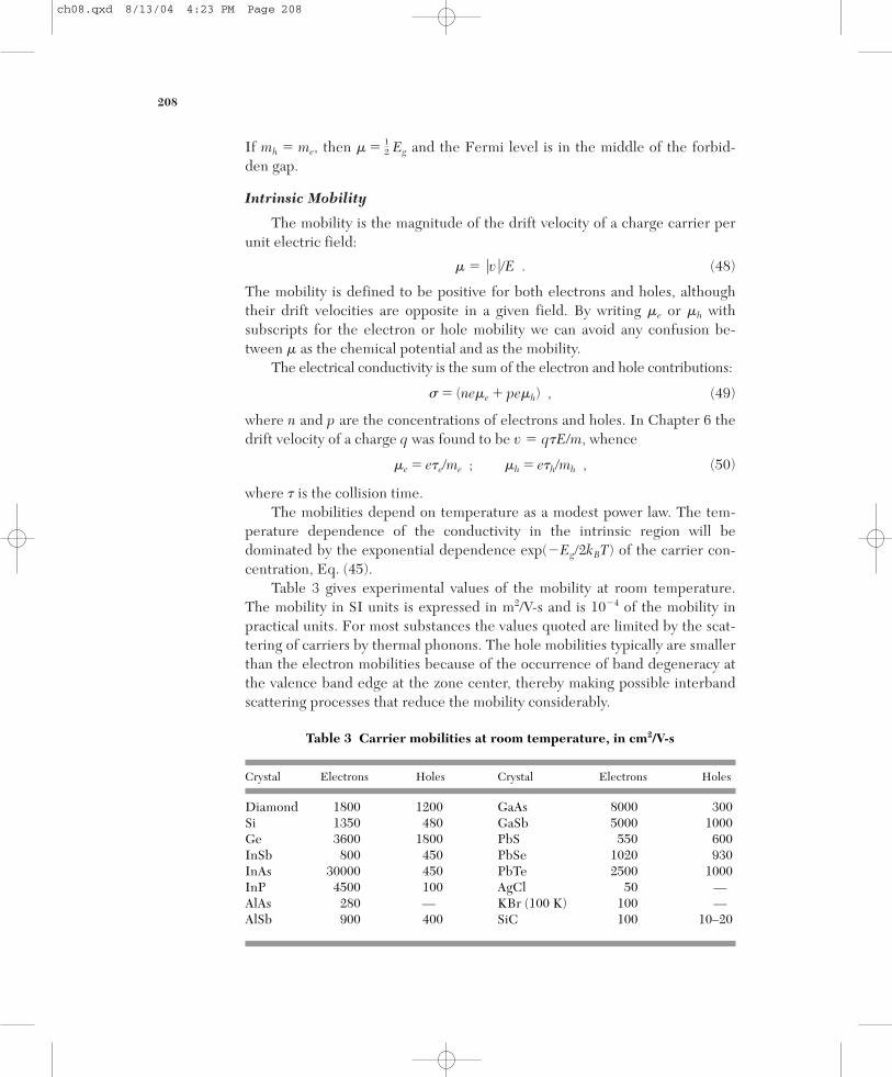
Table 3 Carrier mobilities at room temperature, in cm2/V-s
Crystal Electrons Holes Crystal Electrons Holes
Diamond 1800 1200 GaAs 8000 300Si 1350 480 GaSb 5000 1000Ge 3600 1800 PbS 550 600InSb 800 450 PbSe 1020 930InAs 30000 450 PbTe 2500 1000InP 4500 100 AgCl 50 —AlAs 280 — KBr (100 K) 100 —AlSb 900 400 SiC 100 10–20
ch08.qxd 8/13/04 4:23 PM Page 208

In some crystals, particularly in ionic crystals, the holes are essentiallyimmobile and get about only by thermally-activated hopping from ion to ion.The principal cause of this “self-trapping” is the lattice distortion associated with the Jahn-Teller effect of degenerate states. The orbital degeneracy neces-sary for self-trapping is much more frequent for holes than for electrons.
There is a tendency for crystals with small energy gaps at direct band edgesto have high values of the electron mobility. Small gaps lead to small effectivemasses, which favor high mobilities. The highest mobility observed in a bulksemiconductor is 5 106 cm2/V-s in PbTe at 4 K, where the gap is 0.19 eV.
IMPURITY CONDUCTIVITY
Certain impurities and imperfections drastically affect the electrical prop-erties of a semiconductor. The addition of boron to silicon in the proportion of1 boron atom to 105 silicon atoms increases the conductivity of pure silicon atroom temperature by a factor of 103. In a compound semiconductor a stoichio-metric deficiency of one constituent will act as an impurity; such semiconduc-tors are known as deficit semiconductors. The deliberate addition of impuri-ties to a semiconductor is called doping.
We consider the effect of impurities in silicon and germanium. These ele-ments crystallize in the diamond structure. Each atom forms four covalentbonds, one with each of its nearest neighbors, corresponding to the chemicalvalence four. If an impurity atom of valence five, such as phosphorus, arsenic,or antimony, is substituted in the lattice in place of a normal atom, there willbe one valence electron from the impurity atom left over after the four cova-lent bonds are established with the nearest neighbors, that is, after the impu-rity atom has been accommodated in the structure with as little disturbance aspossible. Impurity atoms that can give up an electron are called donors.
Donor States. The structure in Fig. 19 has a positive charge on the impurityatom (which has lost one electron). Lattice constant studies have verified thatthe pentavalent impurities enter the lattice by substitution for normal atoms,and not in interstitial positions. The crystal as a whole remains neutral becausethe electron remains in the crystal.
The extra electron moves in the coulomb potential e/�r of the impurityion, where � in a covalent crystal is the static dielectric constant of themedium. The factor 1/� takes account of the reduction in the coulomb forcebetween charges caused by the electronic polarization of the medium. Thistreatment is valid for orbits large in comparison with the distance betweenatoms, and for slow motions of the electron such that the orbital frequency islow in comparison with the frequency �g corresponding to the energy gap.These conditions are satisfied quite well in Ge and Si by the donor electron ofP, As, or Sb.
8 Semiconductor Crystals 209
ch08.qxd 8/13/04 4:23 PM Page 209

We estimate the ionization energy of the donor impurity. The Bohr theoryof the hydrogen atom may be modified to take into account the dielectric constant of the medium and the effective mass of an electron in the periodicpotential of the crystal. The ionization energy of atomic hydrogen is in CGS and in SI.
In the semiconductor with dielectric constant � we replace e2 by e2/� andm by the effective mass me to obtain
(51)
as the donor ionization energy of the semiconductor.The Bohr radius of the ground state of hydrogen is in CGS or
in SI. Thus the Bohr radius of the donor is
(52)
The application of impurity state theory to germanium and silicon is com-plicated by the anisotropic effective mass of the conduction electrons. But thedielectric constant has the more important effect on the donor energy becauseit enters as the square, whereas the effective mass enters only as the first power.
To obtain a general impression of the impurity levels we use me 0.1 mfor electrons in germanium and me 0.2 m in silicon. The static dielectricconstant is given in Table 4. The ionization energy of the free hydrogen atom is13.6 eV. For germanium the donor ionization energy Ed on our model is 5 meV,reduced with respect to hydrogen by the factor me/m�2 � 4 10�4. The corresponding result for silicon is 20 meV. Calculations using the correct
��
(SI) ad � 4���0�
2
mee2(CGS) ad � ��2
mee2 � �0.53�
me/m Å ;
4��0�2/me2
�2�me2
(SI) Ed � e4me
2(4���0�)2(CGS) Ed �
e4me
2�2�2 � �13.6�2
mem eV ;
�e4m/2(4��0�)2�e4m�2�2
210
EdEg
0
Donor bound level
�
Si As
Si Si Si
Si Si SiExcess electron from
arsenic atomn-type silicon
Excess+ charge
+
–
Figure 19 Charges associated with an arsenic impurity atom in silicon. Arsenic has five valenceelectrons, but silicon has only four valence electrons. Thus four electrons on the arsenic form tetra-hedral covalent bonds similar to silicon, and the fifth electron is available for conduction. The arsenic atom is called a donor because when ionized it donates an electron to the conduction band.
ch08.qxd 8/13/04 4:23 PM Page 210

anisotropic mass tensor predict 9.05 meV for germanium and 29.8 meV for silicon. Observed values of donor ionization energies in Si and Ge are given inTable 5. In GaAs donors have Ed 6 meV.
The radius of the first Bohr orbit is increased by �m/me over the value 0.53 Å for the free hydrogen atom. The corresponding radius is (160)(0.53) 80 Å in germanium and (60)(0.53) 30 Å in silicon. These are large radii, sothat donor orbits overlap at relatively low donor concentrations, compared tothe number of host atoms. With appreciable orbit overlap, an “impurity band”is formed from the donor states: see the discussion of the metal-insulator tran-sition in Chapter 14.
The semiconductor can conduct in the impurity band by electrons hop-ping from donor to donor. The process of impurity band conduction sets in atlower donor concentration levels if there are also some acceptor atoms pre-sent, so that some of the donors are always ionized. It is easier for a donorelectron to hop to an ionized (unoccupied) donor than to an occupied donoratom, in order that two electrons will not have to occupy the same site duringcharge transport.
Acceptor States. A hole may be bound to a trivalent impurity in germaniumor silicon (Fig. 20), just as an electron is bound to a pentavalent impurity.Trivalent impurities such as B, Al, Ga, and In are called acceptors becausethey accept electrons from the valence band in order to complete the covalentbonds with neighbor atoms, leaving holes in the band.
�
8 Semiconductor Crystals 211
Table 4 Static relative dielectric constant of semiconductors
Crystal � Crystal �
Diamond 5.5 GaSb 15.69Si 11.7 GaAs 13.13Ge 15.8 AlAs 10.1InSb 17.88 AlSb 10.3InAs 14.55 SiC 10.2InP 12.37 Cu2O 7.1
Table 5 Donor ionization energies Ed of pentavalent impurities in germanium and silicon, in meV
P As Sb
Si 45. 49. 39.Ge 12.0 12.7 9.6
ch08.qxd 8/13/04 4:23 PM Page 211
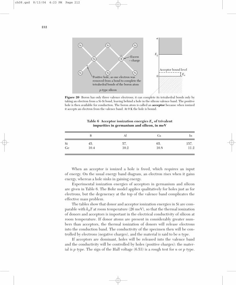
When an acceptor is ionized a hole is freed, which requires an input of energy. On the usual energy band diagram, an electron rises when it gainsenergy, whereas a hole sinks in gaining energy.
Experimental ionization energies of acceptors in germanium and siliconare given in Table 6. The Bohr model applies qualitatively for holes just as forelectrons, but the degeneracy at the top of the valence band complicates theeffective mass problem.
The tables show that donor and acceptor ionization energies in Si are com-parable with kBT at room temperature (26 meV), so that the thermal ionizationof donors and acceptors is important in the electrical conductivity of silicon atroom temperature. If donor atoms are present in considerably greater num-bers than acceptors, the thermal ionization of donors will release electronsinto the conduction band. The conductivity of the specimen then will be con-trolled by electrons (negative charges), and the material is said to be n type.
If acceptors are dominant, holes will be released into the valence bandand the conductivity will be controlled by holes (positive charges): the mater-ial is p type. The sign of the Hall voltage (6.53) is a rough test for n or p type.
212
Table 6 Acceptor ionization energies Ea of trivalent impurities in germanium and silicon, in meV
B Al Ga In
Si 45. 57. 65. 157.Ge 10.4 10.2 10.8 11.2
Ea
Eg
0
Acceptor bound level
�
Si B
Si Si Si
Si Si SiPositive hole, as one electron wasremoved from a bond to complete thetetrahedral bonds of the boron atom
Excess– charge
+
–
p-type silicon
Figure 20 Boron has only three valence electrons; it can complete its tetrahedral bonds only bytaking an electron from a Si-Si bond, leaving behind a hole in the silicon valence band. The positivehole is then available for conduction. The boron atom is called an acceptor because when ionizedit accepts an electron from the valence band. At 0 K the hole is bound.
ch08.qxd 8/13/04 4:23 PM Page 212
Another handy laboratory test is the sign of the thermoelectric potential, dis-cussed below.
The numbers of holes and electrons are equal in the intrinsic regime. Theintrinsic electron concentration ni at 300 K is 1.7 1013 cm�3 in germaniumand 4.6 109 cm�3 in silicon. The electrical resistivity of intrinsic material is43 ohm-cm for germanium and 2.6 105 ohm-cm for silicon.
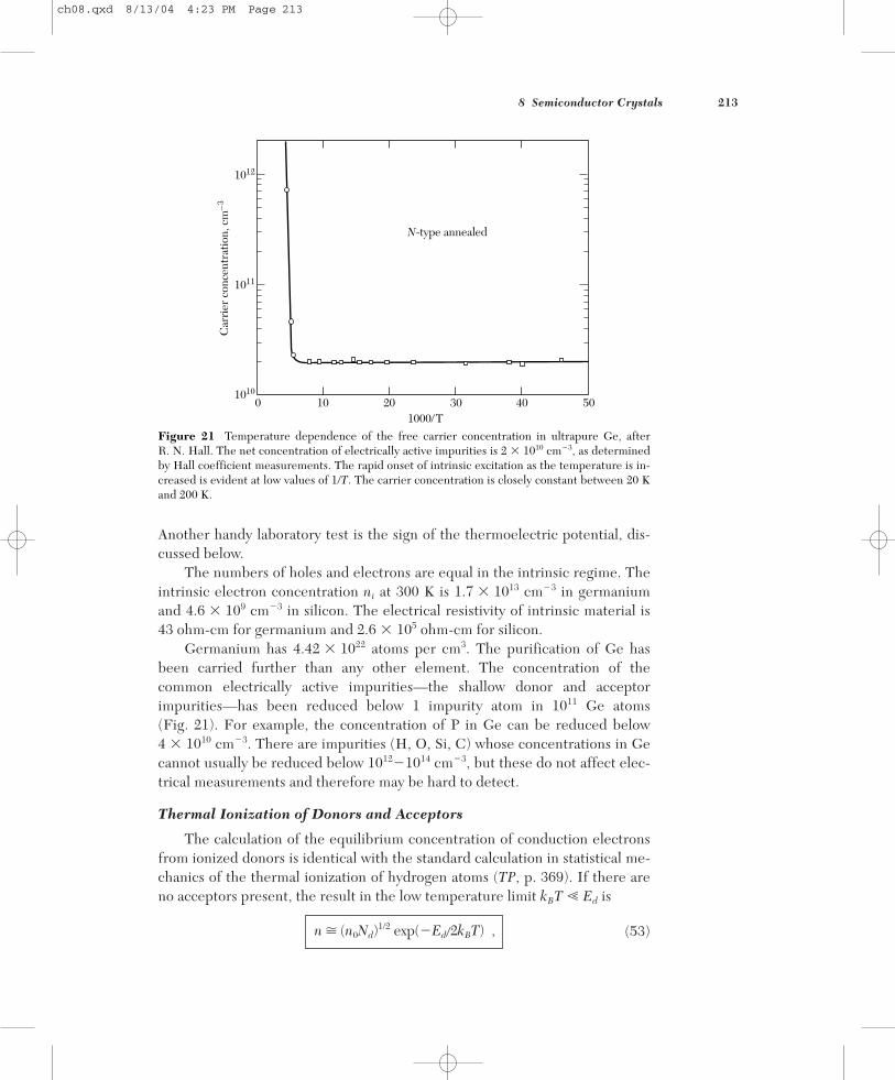
Germanium has 4.42 1022 atoms per cm3. The purification of Ge hasbeen carried further than any other element. The concentration of the common electrically active impurities—the shallow donor and acceptor impurities—has been reduced below 1 impurity atom in 1011 Ge atoms (Fig. 21). For example, the concentration of P in Ge can be reduced below 4 1010 cm�3. There are impurities (H, O, Si, C) whose concentrations in Gecannot usually be reduced below 1012�1014 cm�3, but these do not affect elec-trical measurements and therefore may be hard to detect.
Thermal Ionization of Donors and Acceptors
The calculation of the equilibrium concentration of conduction electronsfrom ionized donors is identical with the standard calculation in statistical me-chanics of the thermal ionization of hydrogen atoms (TP, p. 369). If there areno acceptors present, the result in the low temperature limit kBT � Ed is
(53)n � (n0Nd)1/2 exp(�Ed�2kBT) ,
8 Semiconductor Crystals 213
1010
1011
1012
0 10 20 301000/T
40 50
Car
rier
con
cent
ratio
n, c
m–3
N-type annealed
Figure 21 Temperature dependence of the free carrier concentration in ultrapure Ge, after R. N. Hall. The net concentration of electrically active impurities is 2 1010 cm�3, as determinedby Hall coefficient measurements. The rapid onset of intrinsic excitation as the temperature is in-creased is evident at low values of 1/T. The carrier concentration is closely constant between 20 Kand 200 K.
ch08.qxd 8/13/04 4:23 PM Page 213

with here Nd is the concentration of donors. To obtain(53) we apply the laws of chemical equilibria to the concentration ratio
and then set Identical results hold for acceptors,under the assumption of no donor atoms.
If the donor and acceptor concentrations are comparable, affairs are com-plicated and the equations are solved by numerical methods. However, the lawof mass action (43) requires the np product to be constant at a given tempera-ture. An excess of donors will increase the electron concentration and de-crease the hole concentration; the sum n � p will increase. The conductivitywill increase as n � p if the mobilities are equal, as in Fig. 22.
THERMOELECTRIC EFFECTS
Consider a semiconductor maintained at a constant temperature while anelectric field drives through it an electric current density jq. If the current iscarried only by electrons, the charge flux is
(54)
where �e is the electron mobility. The average energy transported by an elec-tron is referred to the Fermi level �,
(Ec � �) �
32 kBT ,
jq � n(�e)(��e)E � ne�eE ,
[Nd�] � [e] � n.[e][Nd
�]/[Nd],
n0 � 2(mekBT/2��2)3/2;
214
1010107
108
109
1010
1010
1011
1012
1013
1011 1012 1013
Electron concentration, cm–3
Con
duct
ivity
, rel
ativ
e un
its
Hol
e co
ncen
trat
ion,
cm
–3
Conducti
vity
Hole concentration
Figure 22 Electrical conductivity and hole concentration p calculated as a function of electronconcentration n for a semiconductor at a temperature such that np � 1020 cm�6. The conductivityis symmetrical about n � 1010 cm�3. For n � 1010, the specimen is n type; for n � 1010, it is p type.We have taken �e � �h, for the mobilities.
ch08.qxd 8/13/04 4:23 PM Page 214

where Ec is the energy at the conduction band edge. We refer the energy tothe Fermi level because different conductors in contact have the same Fermilevel. The energy flux that accompanies the charge flux is
(55)
The Peltier coefficient � is defined by jU � �jq; or the energy carriedper unit charge. For electrons,
(56)
and is negative because the energy flux is opposite to the charge flux. Forholes
, (57)
where Ev is the energy at the valence band edge. Thus
(58)
and is positive. Equations (56) and (58) are the result of our simple drift veloc-ity theory; a treatment by the Boltzmann transport equation gives minor nu-merical differences.2
The absolute thermoelectric power Q is defined from the open circuitelectric field created by a temperature gradient:
(59)
The Peltier coefficient � is related to the thermoelectric power Q by
(60)
This is the famous Kelvin relation of irreversible thermodynamics. A measure-ment of the sign of the voltage across a semiconductor specimen, one end ofwhich is heated, is a rough and ready way to tell if the specimen is n type or ptype (Fig. 23).
SEMIMETALS
In semimetals the conduction band edge is very slightly lower in energythan the valence band edge. A small overlap in energy of the conduction andvalence bands leads to small concentration of holes in the valence band and ofelectrons in the conduction band (Table 7). Three of the semimetals, arsenic,antimony, and bismuth, are in group V of the periodic table.
Their atoms associate in pairs in the crystal lattice, with two ions and tenvalence electrons per primitive cell. The even number of valence electrons
� � QT .
E � Q grad T .
�h � (� � Ev �
32kBT)/e
jq � pe�hE ; jU � p(� � Ev �
32kBT)�hE
�e � �(Ec � � �
32 kBT)/e
jU � n(Ec � � �
32 kBT)(��e)E .
8 Semiconductor Crystals 215
2A simple discussion of Boltzmann transport theory is given in Appendix F.
ch08.qxd 8/13/04 4:23 PM Page 215

could allow these elements to be insulators. Like semiconductors, the semi-metals may be doped with suitable impurities to vary the relative numbers ofholes and electrons. Their concentrations may also be varied with pressure, forthe band edge overlap varies with pressure.
SUPERLATTICES
Consider a multilayer crystal of alternating thin layers of different composi-tions. Coherent layers on a nanometer thickness scale may be deposited by molecular-beam epitaxy or metal-organic vapor deposition, thus building up a superperiodic structure on a large scale. Systems of alternate layers of GaAs andGaAlAs have been studied to 50 periods or more, with lattice spacing A of per-haps 5 nm (50 Å). A superperiodic crystal potential arises from the superperiodicstructure and acts on the conduction electrons and holes to create new (small)Brillouin zones and mini energy bands superposed on the band structures of the
216
–0.8
–0.6
–0.4
–0.2
0
0.2
0.4
0.6
200 300 400 500Temperature, in K
600 700 800 900
QT
, in
volts
p-type
n-type
(Intrinsic)
Figure 23 Peltier coefficient of n and p silicon as a function of temperature. Above 600 K the spec-imens act as intrinsic semiconduc-tors. The curves are calculated andthe points are experimental. (AfterT. H. Geballe and G. W. Hull.)
Table 7 Electron and hole concentrations in semimetals
Semimetal ne, in cm�3 nh, in cm�3
Arsenic (2.12 � 0.01) 1020 (2.12 � 0.01) 1020
Antimony (5.54 � 0.05) 1019 (5.49 � 0.03) 1019
Bismuth 2.88 1017 3.00 1017
Graphite 2.72 1018 2.04 1018
ch08.qxd 8/13/04 4:23 PM Page 216

constituent layers. Here we treat the motion of an electron in a superlattice in anapplied electric field.
Bloch Oscillator
Consider a collisionless electron in a periodic lattice in one dimension,with motion normal to the planes of the superlattice. The equation of motionin a constant electric field parallel to k is or, for motion across a Brillouin zone with reciprocal lattice vector G � 2�/A, we have
where T is the period of the motion. The Bloch frequency of the motion is The electron accelerates from k � 0 toward the zone boundary; when it reaches k � �/A it reappears (as byan Umklapp process) at the zone boundary at the identical point ��/A, usingthe argument of Chapter 2.
We consider the motion in a model system in real space. We suppose thatthe electron lies in a simple energy band of width �0:
(61)
The velocity in k-space (momentum space) is
(62)
and the position of the electron in real space, with the initial condition z � 0at t � 0, is given by
(63)
This confirms that the Bloch oscillation frequency in real space is The motion in the periodic lattice is quite different from the motion in freespace, for which the acceleration is constant.
Zener Tunneling
Thus far we have considered the effect of the electrostatic potential �eEz(or �eEnA) on one energy band; the potential tilts the whole band. Higherbands will also be tilted similarly, creating the possibility of crossing betweenladder levels of different bands. The interaction between different band levels atthe same energy opens the possibility for an electron in one band at n to cross toanother band at n�. This field-induced interband tunneling is an example ofZener breakdown, met most often at a single junction as in the Zener diode.
SUMMARY
• The motion of a wave packet centered at wavevector k is described bywhere F is the applied force. The motion in real space is ob-
tained from the group velocity vg � �� 1�k�(k).F � �dk�dt,
�B � eEA��.
�(��0
/eE)(cos kA � 1) � (��0
/eE)(cos(�eEAt/�) �1) .
z � �v dt � �dk v(k)(dt/dk) � (A�0/�) �dk(��/eE) sin kA
� ��1d��dk � (A�0��) sin kA ,
� � �0(1�cos kA) .
�B � 2��T � eEA��.�G � �2��A � eET,
�dk�dt � �eE
8 Semiconductor Crystals 217
ch08.qxd 8/13/04 4:23 PM Page 217

• The smaller the energy gap, the smaller is the effective mass |m*| near thegap.
• A crystal with one hole has one empty electron state in an otherwise filledband. The properties of the hole are those of the N � 1 electrons in thisband.(a) If the electron is missing from the state of wavevector ke, then thewavevector of the hole is kh � �ke.(b) The rate of change of kh in an applied field requires the assignment of apositive charge to the hole: eh � e � �ee.(c) If ve is the velocity an electron would have in the state ke, then the veloc-ity to be ascribed to the hole of wavevector kh � � ke is vh � ve.(d) The energy of the hole referred to zero for a filled band is positive and is�h(kh)� ��(ke).(e) The effective mass of a hole is opposite to the effective mass of an elec-tron at the same point on the energy band: mh � �me.
Problems
1. Impurity orbits. Indium antimonide has Eg � 0.23 eV; dielectric constant � � 18;electron effective mass me � 0.015 m. Calculate (a) the donor ionization energy; (b) the radius of the ground state orbit. (c) At what minimum donor concentrationwill appreciable overlap effects between the orbits of adjacent impurity atomsoccur? This overlap tends to produce an impurity band—a band of energy levelswhich permit conductivity presumably by a hopping mechanism in which electronsmove from one impurity site to a neighboring ionized impurity site.
2. Ionization of donors. In a particular semiconductor there are 1013 donors/cm3
with an ionization energy Ed of 1 meV and an effective mass 0.01 m. (a) Estimate theconcentration of conduction electrons at 4 K. (b) What is the value of the Hall coeff-icent? Assume no acceptor atoms are present and that Eg � kBT.
3. Hall effect with two carrier types. Assuming concentration n, p; relaxation timese, h; and masses me, mh, show that the Hall coefficient in the drift velocity approxi-mation is
(CGS)
where b � �e/�h is the mobility ratio. In the derivation neglect terms of order B2. InSI we drop the c. Hint: In the presence of a longitudinal electric field, find thetransverse electric field such that the transverse current vanishes. The algebra mayseem tedious, but the result is worth the trouble. Use (6.64), but for two carriertypes; neglect (�c)2 in comparison with �c.
RH �
1ec �
p � nb2
(p � nb)2 ,
218
ch08.qxd 8/13/04 4:23 PM Page 218

4. Cyclotron resonance for a spheroidal energy surface. Consider the energy surface
where mt is the transverse mass parameter and ml is the longitudinal mass parame-ter. A surface on which �(k) is constant will be a spheroid. Use the equation of mo-tion (6), with to show that �c � eB/(mlmt)1/2c when the static magneticfield B lies in the xy plane. This result agrees with (34) when � � �/2. The result isin CGS; to obtain SI, omit the c.
5. Magnetoresistance with two carrier types. Problem 6.9 shows that in the driftvelocity approximation the motion of charge carriers in electric and magnetic fieldsdoes not lead to transverse magnetoresistance. The result is different with two car-rier types. Consider a conductor with a concentration n of electrons of effective mass me and relaxation time e; and a concentration p of holes of effective mass mh and relaxation time h. Treat the limit of very strong magnetic fields, �c � 1.(a) Show in this limit that �yx � (n � p)ec/B. (b) Show that the Hall field is given by,with Q �c,
which vanishes if n � p. (c) Show that the effective conductivity in the x direction is
If n � p, � B�2. If n p, � saturates in strong fields; that is, it approaches a limitindependent of B as B → .�
��
�eff �
ecB
�� nQe
�
pQh � (n � p)2� n
Qe �
pQh� 1� .
Ey � � (n � p)� nQe
�
pQh� 1
Ex ,
�
v � �� 1�k�,
�(k) � �2�kx2 � ky
2
2mt �
kz2
2ml ,
8 Semiconductor Crystals 219
ch08.qxd 8/13/04 4:23 PM Page 219

ch08.qxd 8/13/04 4:23 PM Page 220