Embed Size (px)
Citation preview

Nanowires
DOI: 10.1002/smll.200500495
Semiconductor Nanowires: From Self-Organization toPatterned GrowthHong Jin Fan, Peter Werner, and Margit Zacharias*
From the Contents
1. Introduction.............701
2. The Growth ofNanowires................703
3. Controlling Position,Arrangement, and Sizeof Catalytic Nuclei forPatterned NanowireGrowth.....................706
4. Patterned NanowireArrays by Non-VLS-based Techniques....712
5. Towards Devices andFunctions.................712
6. Summary and Outlook................................714
Keywords:· nanopatterning· nanowires· self-assembly· semiconductors· template synthesis
Growth of nanowires can be controlled so that ordered arrays can be prepared.
700 www.small-journal.com ( 2006 Wiley-VCH Verlag GmbH&Co. KGaA, D-69451 Weinheim small 2006, 2, No. 6, 700 – 717
reviews M. Zacharias et al.
The synthesis of semiconductor nanowires has been studied intensivelyworldwide for a wide spectrum of materials. Such low-dimensionalnanostructures are not only interesting for fundamental research due to theirunique structural and physical properties relative to their bulk counterparts,but also offer fascinating potential for future technological applications.Deeper understanding and sufficient control of the growth of nanowires arecentral to the current research interest. This Review discusses the variousgrowth processes, with a focus on the vapor–liquid–solid process, whichoffers an opportunity for the control of spatial positioning of nanowires.Strategies for position-controlled and nanopatterned growth of nanowirearrays are reviewed and demonstrated by selected examples as well asdiscussed in terms of larger-scale realization and future prospects. Issues onbuilding up nanowire-based electronic and photonic devices are addressed atthe end of the Review, accompanied by a brief survey of recent progressdemonstrated so far on the laboratory level.
1. Introduction
A number of phenomena in solid-state physics that areclosely related to artificial nanostructured materials havebeen established over the last 15 years. New methods andequipment for high-resolution investigation of solid-statematerials have been developed, which have strongly affect-ed current insight in nature. The first report on carbonnanotubes by Iijima[1] resulted in a worldwide exponentialincrease of research into one-dimensional structures basedon carbon and other materials.
Ongoing device miniaturization and innovative newstructures are major factors for the economical survival ofthe current integrated circuit industry. However, further de-creases in device dimensions are now starting to reach theregime where classical physics becomes invalid and, hence,the function of the circuit might not be guaranteed. A typi-cal example is the leakage problem of ultrathin gate oxidesused in metal–oxide semiconductor (MOS) transistors. Acurrent starts to flow even at an OFF state, which is causedby quantum tunneling of electrons or holes through the thinpotential wells. Today.s dominant ULSI (ultralarge-scale in-tegration) technology for semiconductor structuring is the“top-down” process, which is based on a combination ofphotolithography, thin-film deposition, and etching steps. Ingeneral, the smallest features produced using projection lith-ography are roughly equal to the wavelength of the expo-sure source, for example, 248 nm if using a KrF excimerlaser. Structures below the conventional Rayleigh diffrac-tion limit can be designed with some sophisticated resolu-tion-enhancing techniques with reasonable high controllabil-ity and repeatability. The consensus candidate for the nextphotolithography generation uses the 193-nm line of an ArFlaser. For structures between 100 and 30 nm, electron-beam(e-beam) liACHTUNGTRENNUNGthography is commercially available. Structuringbelow 30 nm, however, goes even beyond the reach of e-beam liACHTUNGTRENNUNGthography to a certain degree. Further minimization
of semiconductor devices requires higher-resolution process-es, which will then involve high production costs for futureproduction lines and sophisticated equipment such as ex-treme ultraviolet lithography. Such technologies are moreand more exhaustive from points of production cost, electri-cal power consumption, and limitations of fundamentalphysics.
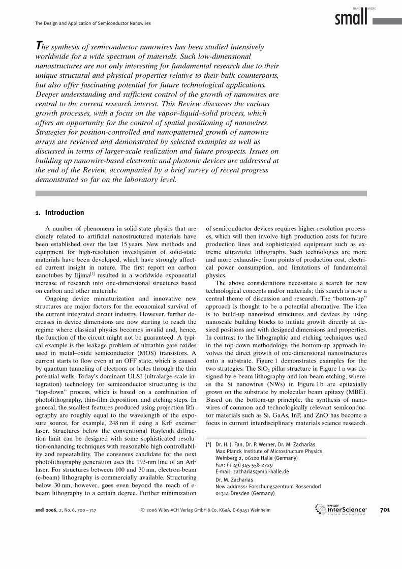
The above considerations necessitate a search for newtechnological concepts and/or materials; this search is now acentral theme of discussion and research. The “bottom-up”approach is thought to be a potential alternative. The ideais to build-up nanosized structures and devices by usingnanoscale building blocks to initiate growth directly at de-sired positions and with designed dimensions and properties.In contrast to the lithographic and etching techniques usedin the top-down methodology, the bottom-up approach in-volves the direct growth of one-dimensional nanostructuresonto a substrate. Figure 1 demonstrates examples for thetwo strategies. The SiO2 pillar structure in Figure 1a was de-signed by e-beam lithography and ion-beam etching, where-as the Si nanowires (NWs) in Figure 1b are epitaxiallygrown on the substrate by molecular beam epitaxy (MBE).Based on the bottom-up principle, the synthesis of nano-wires of common and technologically relevant semiconduc-tor materials such as Si, GaAs, InP, and ZnO has become afocus in current interdisciplinary materials science research.
[*] Dr. H. J. Fan, Dr. P. Werner, Dr. M. ZachariasMax Planck Institute of Microstructure PhysicsWeinberg 2, 06120 Halle (Germany)Fax: (+49)345-558-2729E-mail: [email protected]
Dr. M. ZachariasNew address: Forschungszentrum Rossendorf01314 Dresden (Germany)
small 2006, 2, No. 6, 700 – 717 ( 2006 Wiley-VCH Verlag GmbH&Co. KGaA, D-69451 Weinheim 701
The Design and Application of Semiconductor Nanowires
In this Review, we will look at the growth of semiconductornanowires and describe major trends in research and tech-nology.
The growth of crystals can easily be observed, for exam-ple, as in the case of precipitation out of a supersaturatedsolution by putting a thread into a liquid solution at thestarting point of the crystal growth. The material tends toprecipitate at solid–liquid surfaces upon supersaturation,and such precipitates might have the geometrical form ofneedles. Different ways for locally activating a one-dimen-sional growth mode have been investigated, for example,using local inhomogeneities on the surfaces of substrates. Inthe 1930s, the formation of periodic structures on the mi-ACHTUNGTRENNUNGcrometer scale was observed on crystal surfaces. These for-mations were intensively studied in the following decadesboth experimentally and theoretically to understand moredeeply the ordering of such complex structures and theirgrowth principles.
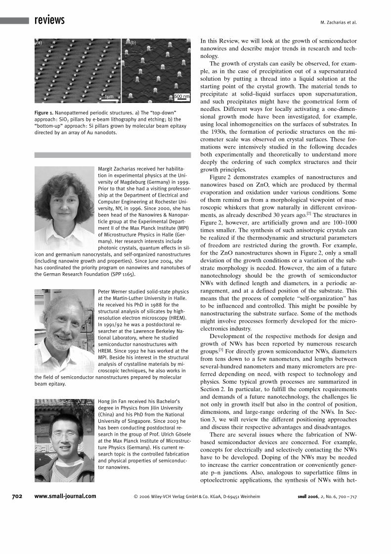
Figure 2 demonstrates examples of nanostructures andnanowires based on ZnO, which are produced by thermalevaporation and oxidation under various conditions. Someof them remind us from a morphological viewpoint of mac-roscopic whiskers that grow naturally in different environ-ments, as already described 30 years ago.[2] The structures inFigure 2, however, are artificially grown and are 100–1000times smaller. The synthesis of such anisotropic crystals canbe realized if the thermodynamic and structural parametersof freedom are restricted during the growth. For example,for the ZnO nanostructures shown in Figure 2, only a smalldeviation of the growth conditions or a variation of the sub-strate morphology is needed. However, the aim of a futurenanotechnology should be the growth of semiconductorNWs with defined length and diameters, in a periodic ar-rangement, and at a defined position of the substrate. Thismeans that the process of complete “self-organization” hasto be influenced and controlled. This might be possible bynanostructuring the substrate surface. Some of the methodsmight involve processes formerly developed for the micro-electronics industry.
Development of the respective methods for design andgrowth of NWs has been reported by numerous researchgroups.[3] For directly grown semiconductor NWs, diametersfrom tens down to a few nanometers, and lengths betweenseveral-hundred nanometers and many micrometers are pre-ferred depending on need, with respect to technology andphysics. Some typical growth processes are summarized inSection 2. In particular, to fulfill the complex requirementsand demands of a future nanotechnology, the challenges lienot only in growth itself but also in the control of position,dimensions, and large-range ordering of the NWs. In Sec-tion 3, we will review the different positioning approachesand discuss their respective advantages and disadvantages.
There are several issues where the fabrication of NW-based semiconductor devices are concerned. For example,concepts for electrically and selectively contacting the NWshave to be developed. Doping of the NWs may be neededto increase the carrier concentration or conveniently gener-ate p–n junctions. Also, analogous to superlattice films inoptoelectronic applications, the synthesis of NWs with het-
Peter Werner studied solid-state physicsat the Martin-Luther University in Halle.He received his PhD in 1988 for thestructural analysis of silicates by high-resolution electron microscopy (HREM).In 1991/92 he was a postdoctoral re-searcher at the Lawrence Berkeley Na-tional Laboratory, where he studiedsemiACHTUNGTRENNUNGconductor nanostructures withHREM. Since 1992 he has worked at theMPI. Beside his interest in the structuralanalysis of crystalline materials by mi-croscopic techniques, he also works in
the field of semiconductor nanostructures prepared by molecularbeam epitaxy.
Hong Jin Fan received his Bachelor’sdegree in Physics from Jilin University(China) and his PhD from the NationalUniversity of Singapore. Since 2003 hehas been conducting postdoctoral re-search in the group of Prof. Ulrich Gçseleat the Max Planck Institute of Microstruc-ture Physics (Germany). His current re-search topic is the controlled fabricationand physical properties of semiconduc-tor nanowires.
Margit Zacharias received her habilita-tion in experimental physics at the Uni-versity of Magdeburg (Germany) in 1999.Prior to that she had a visiting professor-ship at the Department of Electrical andComputer Engineering at Rochester Uni-versity, NY, in 1996. Since 2000, she hasbeen head of the Nanowires & Nanopar-ticle group at the Experimental Depart-ment II of the Max Planck Institute (MPI)of Microstructure Physics in Halle (Ger-many). Her research interests includephotonic crystals, quantum effects in sil-
icon and germanium nanocrystals, and self-organized nanostructures(including nanowire growth and properties). Since June 2004, shehas coordinated the priority program on nanowires and nanotubes ofthe German Research Foundation (SPP 1165).
Figure 1. Nanopatterned periodic structures. a) The “top-down”approach: SiO2 pillars by e-beam lithography and etching; b) the“bottom-up” approach: Si pillars grown by molecular beam epitaxydirected by an array of Au nanodots.
702 www.small-journal.com ( 2006 Wiley-VCH Verlag GmbH&Co. KGaA, D-69451 Weinheim small 2006, 2, No. 6, 700 – 717
reviews M. Zacharias et al.
ACHTUNGTRENNUNGerostructures is also desired in many cases. Furthermore, thepossible role played by the quantum effect should be con-sidered. Such issues related to NW-based device fabricationare discussed in Section 4.
2. The Growth of Nanowires
2.1. The Vapor–Liquid–Solid (VLS) Process
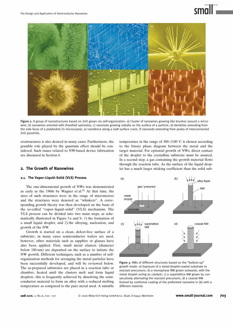
The one-dimensional growth of NWs was demonstratedas early as the 1960s by Wagner et al.[4] At that time, thesizes of such structures were in the range of micrometersand the structures were denoted as “whiskers”. A corre-sponding growth theory was then developed on the basis ofthe so-called “vapor–liquid–solid” (VLS) mechanism. TheVLS process can be divided into two main steps, as sche-matically illustrated in Figure 3a and b: 1) the formation ofa small liquid droplet, and 2) the alloying, nucleation, andgrowth of the NW.
Growth is started on a clean, defect-free surface of asubstrate; in many cases semiconductor wafers are used,however, other materials such as sapphire or glasses havealso been applied. First, small metal clusters (diameterbelow 100 nm) are deposited on the surface to initiate theNW growth. Different techniques, such as a number of self-organization methods for arranging the metal particles havebeen successfully developed, and will be reviewed below.The as-prepared substrates are placed in a reaction tube orchamber, heated until the clusters melt and form liquiddroplets; this is frequently achieved by dissolving the semi-conductor material to form an alloy with a reduced meltingtemperature as compared to the pure metal used. A suitable
temperature in the range of 300–1100 8C is chosen accordingto the binary phase diagram between the metal and thetarget material. For epitaxial growth of NWs, direct contactof the droplet to the crystalline substrate must be assured.In a second step, a gas containing the growth material flowsthrough the reaction tube. As the surface of the liquid drop-let has a much larger sticking coefficient than the solid sub-
Figure 2. A group of nanostructures based on ZnO grown via self-organization: a) Cluster of nanowires growing like brushes around a micro-wire; b) nanowires oriented with threefold symmetry; c) nanorods growing radially on the surface of a particle; d) dendrites extending fromthe side faces of a polyhedral Zn microcrystal; e) nanofence along a GaN surface crack; f) nanorods extending from peaks of interconnectedZnO pyramids.
Figure 3. NWs of different structures based on the “bottom-up”growth mode: a) Exposure of a metal-droplet-coated substrate toreactant precursors; b) a monophase NW grown outwards, with themetal droplet acting as catalyst; c) a superlattice NW grown by con-secutively alternating the reactant precursors; d) a coaxial NWformed by conformal coating of the preformed nanowire in (b) with adifferent material.
small 2006, 2, No. 6, 700 – 717 ( 2006 Wiley-VCH Verlag GmbH&Co. KGaA, D-69451 Weinheim www.small-journal.com 703
The Design and Application of Semiconductor Nanowires
strate, the precursor atoms prefer to deposit on the surfaceof the liquid and forms an alloy. Continued incorporation ofprecursor atoms into the liquid droplet leads to an supersa-turation of the semiconductor component. As a conse-quence, crystal growth occurs at the solid–liquid interfaceby precipitation and NW growth commences. The NW di-ameter is determined by the size of the droplet. The growthrate, however, depends much on the supersaturation, whichcan be influenced by the concentration of precursor vaporand the substrate temperature. The droplet in most cases re-mains at the tip of the NW in the course of the subsequentgrowth, as shown in Figure 3. A direct observation of theVLS growth of Ge nanowires was reported by Wu andYang,[5] who identified the various growth stages in correla-tion to the Au–Ge binary phase diagram. More recently,similar in situ observation of VLS growth of Si NWs byusing ultrahigh-vacuum transmission electron microscopy(UHV TEM) was reported by Ross et al.[6]
In 1992, Hitachi applied the VLS mechanism using golddroplets as catalysts for the growth of III–V NWs, for exam-ple, GaAs and InGaAs.[7] By that time, the doping of wireshad already been demonstrated, which proved the generalpossibility for the formation of p–n junctions within thewires and, hence, for NW-based light-emitting diodes(LEDs). After these pioneering experiments, sparse prog-ress was reported for several years until the Lieber group[8]
at Harvard University reported new activities on the growthof Si NWs based on the Si–Au eutectic. The Si NWs weregrown by chemical vapor deposition (CVD) and were “har-vested” by cutting material from the substrate and thenbringing them into suspension. By using Langmuir–Blodgetttechniques, the individual NWs were assembled parallel tothe surface of a handling substrate, which enabled theLieber group to study basic physical properties of Si NWsand first demonstrate devices such as diodes and biosensors.The Yang group[9] investigated the formation of micropat-terned NWs of ZnO by prepatterning catalytic Au. Thegroup showed for the firsttime the lasing effect ofZnO NWs,[9] whichsparked extensive interestin the fabrication of well-aligned and highly or-dered ZnO NWs or rods.Recently, a large-scale ar-rangement of spatiallyseparated ZnO NWs in ahexagonal pattern wasdemonstrated.[10] In addi-tion, Samuelson concen-trated on the VLS epitax-ial growth of III–V NWsand NW het ACHTUNGTRENNUNGerostructuresand the study of their ap-plication as nanoelectron-ic devices.[11]
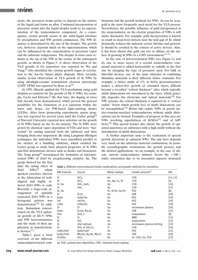
Table 1 gives a briefoverview of the differentsemiconductor/metal com-
binations and the growth methods for NWs. As can be seen,gold is the most frequently used metal for the VLS process.Nevertheless, the possible influence of gold incorporated inthe semiconductor on the electric properties of NWs is stillunder discussion. For example, gold incorporation is knownto result in deep-level defects near the mid gap of Si, whichdrastically reduces the minority carrier lifetime and general-ly should be avoided in the context of active devices. Also,it has been shown that gold can wet or diffuse on the sur-face of growing Si NWs in a UHV environment.[12, 13]
In the case of heterostructural NWs (see Figure 3c andd), one or more layers of a second semiconductor com-pound material is added horizontally or radially to the firstone by changing the type of precursor used. For bulk orthin-film devices, one of the main obstacles in combiningdissimilar materials is their different lattice constants. Forexample, a lattice misfit of 4% in Si/Ge heterostructuresmakes a defect-free growth of extended layers difficultbeyond a so-called “critical thickness” after which typicallymisfit dislocations are introduced in the layer, which gener-ally degrades the electronic and optical materials.[28] ForNW systems, the critical thickness is replaced by a “criticalradius” below which growth free of misfit dislocations canbe accomplished.[29] Below this radius, NWs of poorly lat-tice-constant-matched semiconductors without misfit dislo-cations can be formed. Examples of progress in this area areNWs involving superlattices of Si/SiGe[27] and of InP/InAs.[30] This special feature also allows the growth of epi-taxial nanowires on substrates with a high misfit without theintroduction of misfit dislocations.
A further important issue is the realization of specialgrowth directions in epitaxial NWs. The aim here dependsvery much on the substrate–material combination, its possi-ble crystallographic orientations, the growth process, andthe desired applications. As an example, in the case of sili-con, current semiconductor industry favors the <100>wafer orientation due to its associated superior structural
Table 1. Different semiconductor/metal combinations and growth methods for nanowires.
NW material Source Metal catalyst Growth process[a] Ref.
Si SiCl4 Au CVD ACHTUNGTRENNUNG[14,15]Si SiCl4 Au, Ag, Cu, Pt CVD [4]Si, Ge SiH4, GeH4 Au CVD [16]Si SiH4 Au CVD [17]Si, Ge Fe, Si/Fe, Ge/Fe PLD [8]Si Si2H6 Au CBE [18]GaAs GaAs/Au Au PLD [19]InP InP/Au Au PLD [19]CdSe CdSe/Au Au PLD [19]Si Si Ga microwave plasma [20]GaAs Et3Ga, Bu3As Au CBE [21]ZnO ZnO, C Au evaporation [9]Si Si Au MBE [12]Si SiO Au evaporation [22]Si silyl radicals Ga microwave plasma etching [23]Si SiH4 or SiH2Cl2 Ti CVD [24]GaAs/GaP GaAs/GaP Au PLD [25]GaAs/InAs Me3Ga, Bu3As, Me3In Au CBE [26]Si/SiGe SiCl4 Au Si: CVD; Ge: PLD [27]
[a] PLD: pulsed laser deposition; CBE: chemical beam epitaxy.
704 www.small-journal.com ( 2006 Wiley-VCH Verlag GmbH&Co. KGaA, D-69451 Weinheim small 2006, 2, No. 6, 700 – 717
reviews M. Zacharias et al.
and processing behavior and its electronic properties. How-ever, VLS growth of Si NWs has until now been mainly suc-cessful in the <111> and <110> directions. In addition,there appears to be a diameter dependence on the growthdirection.[31,32] The epitaxial growth of Si NWs using a CVDsystem results in a preferred <111> growth direction forwire diameters larger than 20 nm and a <110> orientationfor diameters smaller than 20 nm. This behavior holds forepitaxial and nonepitaxial growth.[31, 32] This can be mainlyunderstood in terms of the influence of surface and inter-face energies of the respective material combinations inVLS growth. Another nice example is given by Kuykendallet al. ,[33] who reported GaN nanowires with two types ofgrowth orientations, namely [11̄00] and [0001]. Substrateswith different crystallographic orientations but having goodlattice matching to GaN were chosen to induce the NWgrowth in specific orientations. The driving force behind thiswas an interface epitaxy at the nucleation stage of the VLSprocess.[33]
2.2. The Vapor–Solid (VS) Process
NWs can also be grown without extra metal catalysts bythermally evaporating a suitable source material near itsmelting point and then depositing at cooler temperatures.[34]
Such a self-organization process, which does not involveliquid droplets as the catalyst, is referred to as a “vapor–solid” (VS) mechanism. In many cases, the growth mecha-nism works in an analogous way to the VLS process, differ-ing in that here one component of the gaseous atoms mightplay the role of the catalyst itself.[35] Common examples arethe formation of ZnO and Ga2O3 NWs. Either the precursorgas is decomposed due to a high reaction temperature orthe pure metal (Zn and Ga) powder is evaporated under asuitable flow gas atmosphere.[36, 37] Zn and Ga are character-ized by low melting points and sublimation temperatures,which are comparable to the temperatures in the reactionchamber. Therefore, a segregate at the surface of the sub-strate, especially at places with inhomogeneties or defects,or at the cooler parts of the tube walls, is very probable. Inthe case of ZnO when oxygen is added to the reactionchamber, the liquid droplets solidify quickly by oxidationand the formation of ZnO wires can eventually be observed.A similar “decoration” of surface defects has been reportedfor GaN NWs formed on Si substrates. In the VS growthmode, control of the NW diameter is accomplished mainlyby changing the evaporation and collection temperatures, aswell as the vapor pressure. While fabrication of various hier-archical semiconductor nanostructures through the VSgrowth mode has been reported in the literature,[34,38] notight control of the spatial arrangement has been achievedso far.
2.3. Electrochemical Deposition
In addition to the physical vapor-growth modes de-ACHTUNGTRENNUNGscribed above, NWs may also be grown by electrochemical
deACHTUNGTRENNUNGposition methods in combination with templates such asporous anodic aluminum oxide (AAO), nano-channel glass,and porous polymer films self-organized from diblock co-polymers. The template is attached to the cathode, which issubsequently brought into contact with the deposition solu-tion. The anode is placed in the deposition solution parallelto the cathode. When an electric field is applied, cations dif-fuse towards and reduce at the cathode, resulting in thegrowth of nanowires inside the pores of the template. Afterpore filling, free-standing nanowires can be obtained by dis-solution of the template membrane. The length of the pores,which can be tuned by the etching process, determines thenthe length of the NWs. The most widely used templates forelectrochemical deposition of NWs is AAO, which has beenused for the fabrication of a wide range of NW materials in-cluding mainly metals, conductive polymers, and metaloxide materials,[39-41] as well as multisegmented NWs.[42] Forsemiconductors, the electrochemical deposition techniquewas used in 1996 for fabricating arrays of CdS NWs withlengths up to 1 mm and diameters as small as 9 nm.[43] Morerecently, Xu et al.[44, 45] reported a group of II–IV semicon-ductor NW arrays (CdS, CdSe, and CdTe) by dc electro-chemical deposition in porous AAO.
As a further step, the pores in the templates/membranescan be regularly arranged and have a cylindrical shape of aconstant diameter. This is achieved by imprinting the alumi-num surface prior to the anodization process with a litho-graphically prefabricated stamp to generate specific ar-rangements of pores, as will be discussed below.[46] Conse-quently, the resulting NWs are characterized by a narrowsize distribution.[47]
Self-organization of metal and semiconductor NWs canalso occur by electrochemical step-edge decoration ofhighly-oriented pyrolytic graphite surfaces, as demonstratedby the Penner group.[48-50] This represents a facile large-scaleapproach to fabricate supported NWs. When combined withmodern nanolithography techniques,[51] this method can bepotentially extended to horizontally aligned NWs of variousshapes. However, while the material produced by this tech-nique is limited mainly to metals, a second chemical reac-tion of the metal NWs is needed in order to transform theminto semiconductors.[52]
The key issue for semiconductor NWs fabricated byelectrochemical deposition is the crystalline quality. In mostcases the NWs are not epitaxially grown and hence areeither amorphous or polycrystalline in structure. They con-sist of small crystals with an abundance of defects, whichmight limit their technical application, especially in optics.
2.4. Solution Growth
The synthesis of nanocrystals by solution methods iswell known for the II–VI materials.[53] The ability to system-atically manipulate the shapes of such inorganic nanocrys-tals is an important goal in materials chemistry today. Theformation of CdSe nanorods with aspect ratios of 30 werereported by, for example, Manna et al.,[54] who also investi-gated influential factors in shape control. In recent years,
small 2006, 2, No. 6, 700 – 717 ( 2006 Wiley-VCH Verlag GmbH&Co. KGaA, D-69451 Weinheim www.small-journal.com 705
The Design and Application of Semiconductor Nanowires
there have been an increasing number of reports on the sol-ution growth of NWs. Holmes et al.[55] used a supercriticalfluid solution-phase approach to the growth of Si NWs, in-cluding a diameter control by using dodecanethiol-cappedAu nanocrystals. In a similar way, Hanrath and Korgel[56]
grew Ge NWs using alkanethiol-protected Au nanocrystalsas seeds. The growth of ZnO NWs onto various substratesusing thermal decomposition of methylamine and zinc ni-trate in aqueous solution were reported by severalgroups.[57–60] In particular, a multistep, seeded-growth tech-ACHTUNGTRENNUNGnique developed by the Liu and co-workers[61] allows controlof the sequential nucleation and growth, leading to complexnanostructures composed of hierarchical nanorods. Overall,solution methods provide little control over the area densityand the NWs have smaller aspect ratios than those grownby vapor-phase routes. Even worse, the NWs display poorvertical alignment although they exhibit certain texture. Incase of ZnO, the growth and alignment direction is mainlyalong the c axis, which is detrimental to the UV lasing per-formance of ZnO NW arrays. The main advantage of suchsolution-based methods might be the possibility to createNW arrays at low temperatures on large scales at low cost,and on various (even flexible) substrates.[59]
3. Controlling Position, Arrangement, and Size ofCatalytic Nuclei for Patterned NanowireGrowth
The patterning of semiconductor and other surfaces in aperiodic fashion is of great interest for industrial applica-tions. The term “nanopatterning” refers to approaches thatprovide periodic arrangements with feature sizes and latticeconstants below 100 nm. The technological interest in theongoing search for new nanopatterning techniques is basedon the desire for inexpensive methods to pattern areas onthe square-centimeter scale, and beyond. These methodsshould also be easier to realize than conventional e-beamlithography. Most of the methods are still at the laboratorystage, however, the possibility of parallel sequenced writingbased on such nanopatterning methods has already beenpredicted. The realization of patterned metal arrays as cata-lysts for the growth of semiconductor NWs is a new applica-tion of the nanopatterning techniques. In this respect, themetal-catalyst arrays function as a template for the subse-quent growth of NWs via the VLS model, so that the NWswould have the same pattern as the metal dots and the di-ameters of the nanowires are correlated to the size of thecatalyst dots. Therefore, when position control of spatiallyseparated NWs is desired, nanopatterning techniquesbecome essential. In the following section, we will reviewsome typical approaches that have been demonstrated, orare potentially applicable, for position- and size-control ofsemiconductor NWs.
Gold-dot arrays are preferred for the positioning ofNWs, but other metals have also been tested. Table 1 pro-vides an overview for the material combinations and pro-ACHTUNGTRENNUNGcesses used. As high temperatures in the range of 500–1000 8C are usually needed for the growth of semiconductor
NWs, the problem of high mobility and diffusion of themetals, which can destroy the predefined catalyst pattern,has to be solved for the controlled growth of NW arrays. Anumber of patterning and templating methods can be ap-plied for the controlled preparation of metal dots or metal-dot arrays on a substrate surface, including photo- or e-beam lithography, manipulation of single gold nanodots, ar-rangement of Au nanocrystals from suspensions, nanospherelithography, gold deposition masks based on porous aluminatemplates, nanoimprint lithography, block copolymers fornanolithography, as well as other catalyst-positioning ap-proaches. All of these above methods are distinguished bythe effort required and their ability to pattern over a largearea, as discussed below.
3.1. Photolithography or e-Beam Lithography
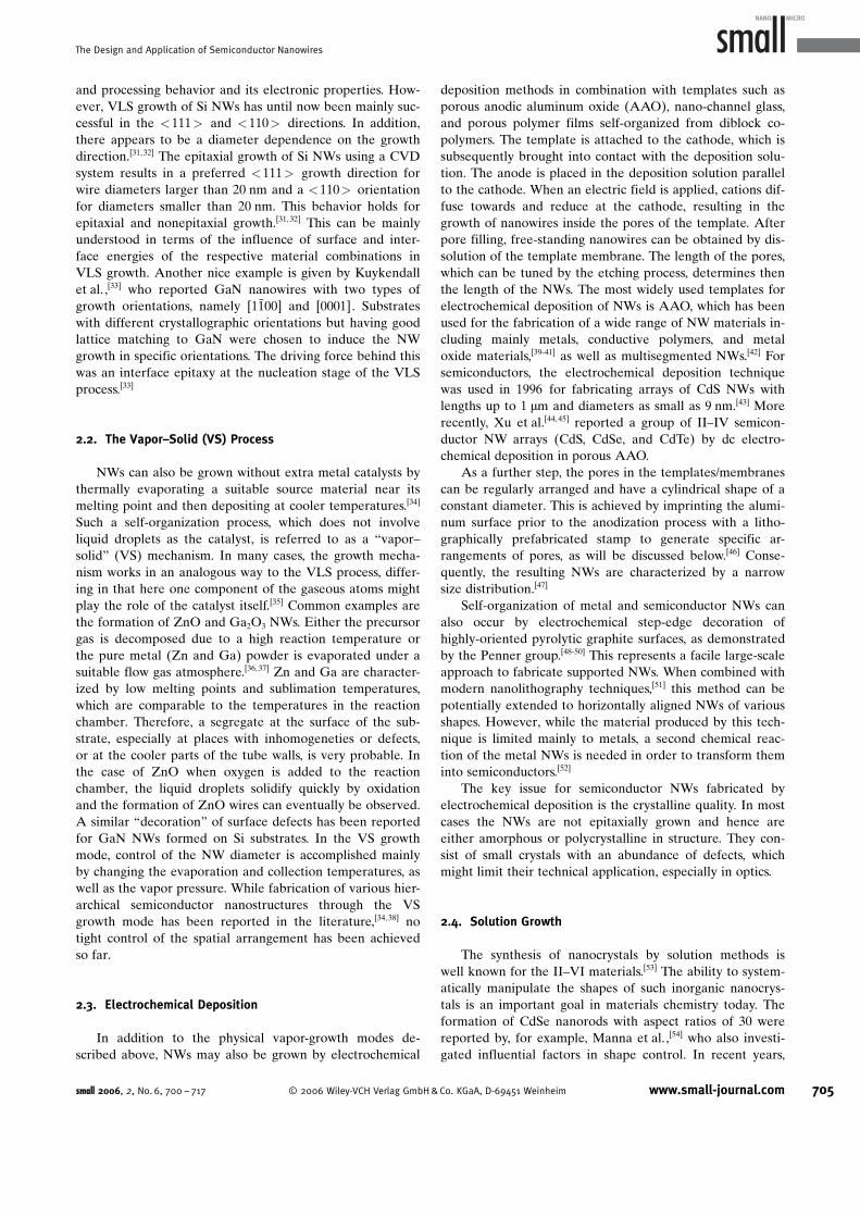
Greyson et al.[62] used a phase-shift photolithographyprocedure for the patterned growth of ZnO NWs. Here,masks containing lines with variable spacing were usedtwice, with rotated orientations, for exposures of positive-tone photoresist. The resulting pattern was transferred byisotropic wet etching into a rather thick gold film, resultingin ordered arrays of Au pads (see FigACHTUNGTRENNUNGure 4a). The advantagewith this technique is that the gold pads can be patternedon a large (square inch) scale with variable symmetry(square, hexagonal, and rectangular) and spacing. However,the grown NWs demonstrated in their work are not straightor uniformly oriented. Several wires (up to 20) with diame-ters of 10–15 nm grow from one defined Au site (see Fig-ure 4b). The behavior is caused by the large size (50–200 nm) and thickness (15–20 nm) of the Au pads used, aswell as the use of a-plane sapphire as the substrate.
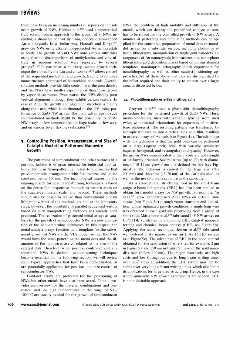
As a conventional structuring tool in the sub-100 nmrange, e-beam lithography (EBL) has also been applied toobtain Au nanodot arrays for NW growth. For example, Nget al.[63] grew nanopatterned ZnO NWs on 6H-SiC sub-strates (see Figure 5a) through vapor transport and deposi-tion. Under optimized growth conditions, a single long wirewas obtained at each gold site protruding from a group ofshort rods. MMrtensson et al.[64] fabricated InP NW arrays onInPACHTUNGTRENNUNG(111)B substrates by combining EBL catalyst nanopat-terning and chemical beam epitaxy (CBE, see Figure 5b).Applying the same technique, Jensen et al.[65] fabricatedwell-ordered InAs nanowires on an InAs (111)B surface(see Fig ACHTUNGTRENNUNGure 5c). The advantage of EBL is the good controlobtained for the separation of wire sites, for example, 2 mmin Fig ACHTUNGTRENNUNGure 5a and 250 nm in Figure 5b, and of the gold nano-disk size (below 100 nm). The major drawbacks are highcosts and low throughput due to long beam writing timesover mm2 areas. In addition, the EBL system may not bestable over very long e-beam writing times, which also limitsits applications for large-area structuring. Hence, in the casewhere numerous NW growth experiments are needed, EBLis not a desirable approach.
706 www.small-journal.com ( 2006 Wiley-VCH Verlag GmbH&Co. KGaA, D-69451 Weinheim small 2006, 2, No. 6, 700 – 717
reviews M. Zacharias et al.
3.2. Manipulation of Single Gold Nanodots
The manipulation of single Au nanodots on the surfaceof a substrate for the site-specific growth of GaAs NWs wasreported by Ohlsson et al.[66] Such single dots were posi-tioned point-by-point on small areas of the substrate. In thecase of NW growth, the critical issue of this method is con-tamination, which should be avoided between the substratesurface and the gold crystals. In particular, any thin film ofamorphous oxide that may be present has to be removedbecause it would hinder epitaxial growth of the NWs. In thisrespect, the positioning of the gold nanodots has to be car-ried out under ultrahigh vacuum including an in situ trans-port of the substrates to the growth chamber. Therefore,
this technique can be usedfor a feasibility study but isnot really suitable from thepoint of view of technologydevelopment since theoutput of nanodevices isvery limited by the ap-proach.
3.3. Arrangements of AuNanocrystals fromSuspensions
Suspensions of goldcrystallites can be receivedfrom a number of suppliersand are characterized by anarrow size distribution.The advantage of usinggold suspensions is the sizecontrol and the possibilityto realize dot diametersbelow �50 nm without anyneed for lithography. Solu-
tions of Au nanocrystals of sizes down to 2 nm are available.Therefore, the NW diameters are also tunable in a preciseway while keeping the other growth parameters constant. Inaddition, the number density of the wires can be varied byusing colloids of different concentrations. The importantfactors for a homogenous coating of a substrate are the sur-face properties of the substrates (hydrophilic, hydrophobic)and the type of solvent used for the suspension, whichshould help to prevent the agglomeration of the nanocrys-tals during drying up. This could be achieved by using an in-termediate layer such as poly-l-lysine.[67] In this case, thenegatively charged nanoclusters stick to the positivelycharged poly-l-lysine. However, such an intermediate layerprevents epitaxial growth of the wires. Si NWs obtained
Figure 5. NW arrays growing from Au pads fabricated using e-beam lithography. a) ZnO NWs of 40-nm diameter grown from Au pads (200 nmwide and 1.5–2 nm thick). Reprinted with permission.[63] b) Tapered InP NWs (tip diameter: 50 nm) grown from Au pads (45 nm wide and17 nm thick). Reprinted with permission.[64] c) InAs NWs of 80-nm diameter and an interwire distance of 750 nm. Reprinted with permission.[65]
All scale bars: 1 mm.
Figure 4. a) Schematic diagram depicting the patterning of catalytic gold dots through phase-shift photoli-thography and etching, and the growth of NWs. b) An example of the ZnO NWs in a hexagonal array. Inset:the corresponding initial gold pattern (area: 12D12 mm2). Reproduced from Ref. [62].
small 2006, 2, No. 6, 700 – 717 ( 2006 Wiley-VCH Verlag GmbH&Co. KGaA, D-69451 Weinheim www.small-journal.com 707
The Design and Application of Semiconductor Nanowires
with this procedure were like a “nanowool”, but had a sizesimilar to the Au nanocrystals used.
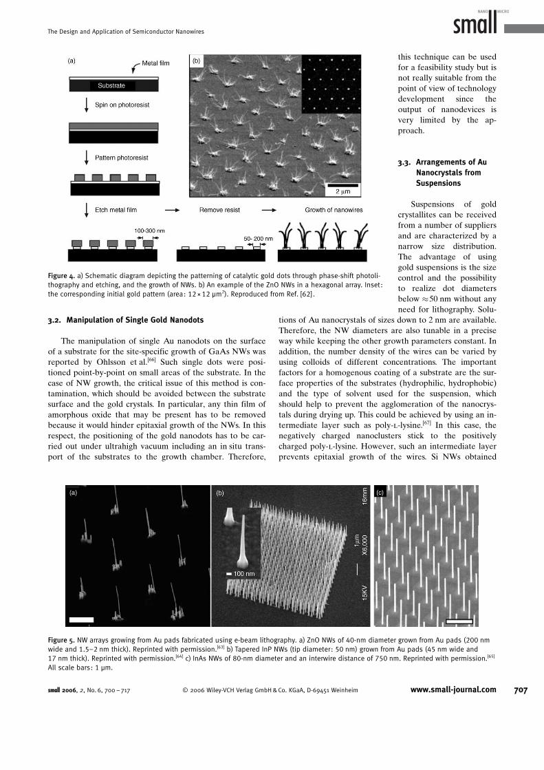
Precautions should also be taken to eliminate the amor-phous native oxide of the substrate if epitaxial growth is de-sired. Very recently, Yang and co-workers successfully grewepitaxial Si NWs on Si substrates using gold colloids of dif-ferent diameters and solution concentrations (seeFigure 6).[68] The colloids were immobilized by coating theSi surface with a thin layer of a polyelectrolyte, which pro-vides electrostatic attraction to the Au colloids. The polymerand the native oxide were removed in situ during thegrowth of the Si NWs by high-temperature annealing andgaseous HCl etching, respectively. Concerning the patternedgrowth, the main problem of using Au suspensions is itslack of controllable ordering of the Au nanocrystals on thesubstrate surface. Nevertheless, sub-micrometer patterningcan still be realized if an additional lithography process isinvolved (see below).
3.4. Nanosphere Lithography
The self-organization of sub-micrometer spheres into amonolayer with a hexagonal close-packed structure is thebasis of the so-called nanosphere lithography (NSL).[69] Typ-ical materials used for the spheres are silica and polystyrene,which are commercially available with narrow size distribu-tions. The deposition of a single layer of the spheres on asubstrate can be used as a lithography shadow mask andtemplate to nanostructure the substrate surface. After thespheres are dissolved (using hydrofluoric acid for SiO2
spheres and acetone for polystyrene), a honeycomb patternof triangular metal islands is obtained. The smaller thespheres the shorter the distance of the metal islands and thesmaller their dimension. This approach can produce hexago-nal arrays of more than1 cm2 with defect-freesingle domains of up to100O100 mm.[70] Further-more, other patterns canalso be realized if morethan one nanosphere layeror a combination ofspheres with different sizesare deposited.[71] NSLoffers a simple, cost-effec-tive, and high-throughputlithographical approach,and has been widely utiliz-ed for the fabrication of awealth of nanostructurearrays, including semicon-ductor NWs.
Figure 7a shows ZnONW arrays on a sapphiresurface fabricated by Wanget al. using monolayerNSL.[72] The initial honey-comb pattern of Au islands
Figure 6. a,c,e) SEM images of Si NWs grown from 50, 30, and20 nm (nominally) Au colloids, respectively. Scale bars are 1 mm.b,d, f) Size distributions of Au colloids and the resulting Si NW diam-eters. Reprinted with permission.[68]
Figure 7. Arrays of ZnO NWs grown from a Au nanodot template fabricated by NSL; a) NW arrays correspondto monolayer NSL. Inset: a top view of the NWs, showing the honeycomb pattern. Reproduced with permis-sion.[72] b) NW arrays grown on a Ni nanodot template arranged in a higher-order pattern by bilayer NSL. Therelative angle between the two sphere monolayers are 2, 7, and 108 from left to right. Reproduced with per-mission.[71]
708 www.small-journal.com ( 2006 Wiley-VCH Verlag GmbH&Co. KGaA, D-69451 Weinheim small 2006, 2, No. 6, 700 – 717
reviews M. Zacharias et al.
was preserved after the NW growth. However, as the size ofthe initial gold islands is much larger than the NW diame-ters (50–150 nm), a cluster of wire appears at each latticesite, forming an interconnected NW network. Rybczynskiet al.[71] demonstrated the growth of ZnO NWs in varioussuperarrays by using bilayers for Ni deposition and adjustingthe relative angles between the two polystyrene monolayers(see Figure 7b). In both cases, the used substrates were a-plane sapphire. The ZnO NWs grow mainly vertical to thesubstrate surface while some unwanted inclined NWs alsoappear. This seems to be an intrinsic problem if using a-plane sapphire as the epitaxial substrate, which is relatedeither to an epitaxial growth of ZnO in vicinal crystallo-graphic equivalent orientations, or to the wetting propertyof ZnO on sapphire at the initial nucleation stage.
In contrast, Fan et al.[73] used GaN epilayers grown on Sias substrates for ZnO nanowire growth. GaN is a suitablesubstrate for the heteroepitaxial growth of ZnO NWs be-cause of their similar optical bandgap energy (�3.4 eV),low misfit of the lattice constant (1.9%), and potential forp-GaN/n-ZnO nano-heterojunctions. However, the GaNsurface is hydrophobic, which prevents the direct self-assem-bly of polystyrene spheres. To overcome this problem, a“mask-transfer” technique was used by Fan et al. to transferthe sphere layers from a hydrophilic SiO2 substrate to theGaN/Si substrates.[73] Figure 8 schematically shows the modi-fied NSL process and examples of such ZnO NWs grown ona GaN epilayer. The hexagonal and triangular lattices of theresulting NW arrays (Figure 8b–e) correspond to monolayerand bilayer NSL, respectively. Advantages of this mask-transfer technique include: 1) the transfer is substratefriendly, and 2) the intersphere holes are narrowed by themetal coating, which results in size reduction (down to30 nm compared to 100 nm in usual cases) and a good sepa-ration of the deposited Au nanodots. This is highly desirable
for size-specific individual NW arrays on conductive sub-strates, as needed for device applications such as sensor orfield-emitter arrays.
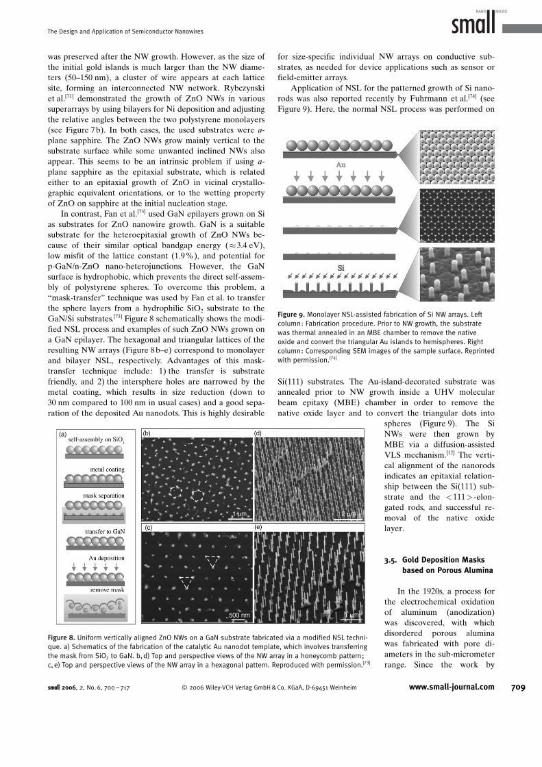
Application of NSL for the patterned growth of Si nano-rods was also reported recently by Fuhrmann et al.[74] (seeFigure 9). Here, the normal NSL process was performed on
SiACHTUNGTRENNUNG(111) substrates. The Au-island-decorated substrate wasannealed prior to NW growth inside a UHV molecularbeam epitaxy (MBE) chamber in order to remove thenative oxide layer and to convert the triangular dots into
spheres (Figure 9). The SiNWs were then grown byMBE via a diffusion-assistedVLS mechanism.[12] The verti-cal alignment of the nanorodsindicates an epitaxial relation-ship between the SiACHTUNGTRENNUNG(111) sub-strate and the <111> -elon-gated rods, and successful re-moval of the native oxidelayer.
3.5. Gold Deposition Masksbased on Porous Alumina
In the 1920s, a process forthe electrochemical oxidationof aluminum (anodization)was discovered, with whichdisordered porous aluminawas fabricated with pore di-ameters in the sub-micrometerrange. Since the work by
Figure 8. Uniform vertically aligned ZnO NWs on a GaN substrate fabricated via a modified NSL techni-que. a) Schematics of the fabrication of the catalytic Au nanodot template, which involves transferringthe mask from SiO2 to GaN. b,d) Top and perspective views of the NW array in a honeycomb pattern;c,e) Top and perspective views of the NW array in a hexagonal pattern. Reproduced with permission.[73]
Figure 9. Monolayer NSL-assisted fabrication of Si NW arrays. Leftcolumn: Fabrication procedure. Prior to NW growth, the substratewas thermal annealed in an MBE chamber to remove the nativeoxide and convert the triangular Au islands to hemispheres. Rightcolumn: Corresponding SEM images of the sample surface. Reprintedwith permission.[74]
small 2006, 2, No. 6, 700 – 717 ( 2006 Wiley-VCH Verlag GmbH&Co. KGaA, D-69451 Weinheim www.small-journal.com 709
The Design and Application of Semiconductor Nanowires
Masuda and Fukuda in 1995,[75] the systematic use of AAOnanopore arrays for nanotechnology has evolved. These re-searchers observed that ordered domains of Al2O3 poreswere established under certain conditions. If the self-organi-zation process is combined with a lithographic prestructur-ing of the aluminum surface, one can force the pores intomonodomain hexagonal order over a cm2 range, that is, on amacroscopic scale.[46] Free-standing AAO membranes canalso be formed and used as metal deposition masks. Howev-er, such membranes should be reasonably thick due to sta-bility problems with the brittle porous alumina materialand, hence, shadowing effects occur if they are used directlyfor a masking procedure.
The application of AAO membranes as lithographyshadow masks for Au deposition was performed by Wuet al.[76] for MBE growth of GaAs NWs on a GaAs (111)Bsubstrate, and by Chik et al.[77] for the growth of ZnO NWson a GaN substrate. In both cases, the free-standing thinAAO templates (150–200 nm and 500 nm, respectively)were transferred directly onto the substrates via van deWaals bonding. The obtained NWs exhibited a much nar-rower diameter distribution than those grown by using agold film. A careful examination of the SEM images showthat the NWs were polydomain ordered and tended tomerge due to their small spatial separations.
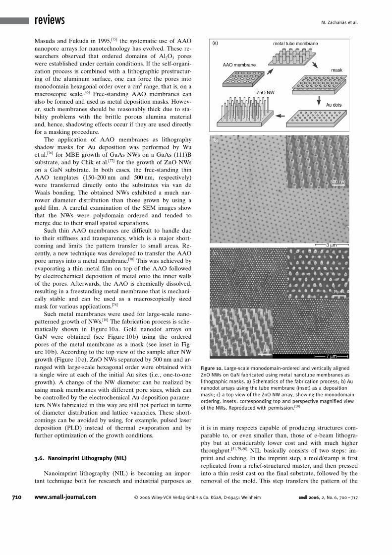
Such thin AAO membranes are difficult to handle dueto their stiffness and transparency, which is a major short-coming and limits the pattern transfer to small areas. Re-cently, a new technique was developed to transfer the AAOpore arrays into a metal membrane.[78] This was achieved byevaporating a thin metal film on top of the AAO followedby electrochemical deposition of metal onto the inner wallsof the pores. Afterwards, the AAO is chemically dissolved,resulting in a freestanding metal membrane that is mechani-cally stable and can be used as a macroscopically sizedmask for various applications.[78]
Such metal membranes were used for large-scale nano-patterned growth of NWs.[10] The fabrication process is sche-matically shown in Figure 10a. Gold nanodot arrays onGaN were obtained (see Figure 10b) using the orderedpores of the metal membrane as a mask (see inset in Fig-ACHTUNGTRENNUNGure 10b). According to the top view of the sample after NWgrowth (Figure 10c), ZnO NWs separated by 500 nm and ar-ranged with large-scale hexagonal order were obtained witha single wire at each of the initial Au sites (i.e., one-to-onegrowth). A change of the NW diameter can be realized byusing mask membranes with different pore sizes, which canbe controlled by the electrochemical Au-deposition parame-ters. NWs fabricated in this way are still not perfect in termsof diameter distribution and lattice vacancies. These short-comings can be avoided by using, for example, pulsed laserdeposition (PLD) instead of thermal evaporation and byfurther optimization of the growth conditions.
3.6. Nanoimprint Lithography (NIL)
Nanoimprint lithography (NIL) is becoming an impor-tant technique both for research and industrial purposes as
it is in many respects capable of producing structures com-parable to, or even smaller than, those of e-beam lithogra-phy but at considerably lower cost and with much higherthroughput.[51, 79,80] NIL basically consists of two steps: im-print and etching. In the imprint step, a mold/stamp is firstreplicated from a relief-structured master, and then pressedinto a thin resist cast on the final substrate, followed by theremoval of the mold. This step transfers the pattern of the
Figure 10. Large-scale monodomain-ordered and vertically alignedZnO NWs on GaN fabricated using metal nanotube membranes aslithographic masks. a) Schematics of the fabrication process; b) Aunanodot arrays using the tube membrane (inset) as a depositionmask; c) a top view of the ZnO NW array, showing the monodomainordering. Insets: corresponding top and perspective magnified viewof the NWs. Reproduced with permission.[10]
710 www.small-journal.com ( 2006 Wiley-VCH Verlag GmbH&Co. KGaA, D-69451 Weinheim small 2006, 2, No. 6, 700 – 717
reviews M. Zacharias et al.
mold into the resist film. The etching step is the patterntransfer from the resist film to the underlying substrate. Fornanopatterning of metals, chemical functionalization of themold and/or the substrate, or a metal-film deposition proc-ess is usually an additional requirement. NIL can be com-bined with other techniques such as nanosphere lithographyand colloidal crystals to produce diverse patterns with ad-justable pitches and feature sizes,[81,82] which further increas-es its flexibility and capability.
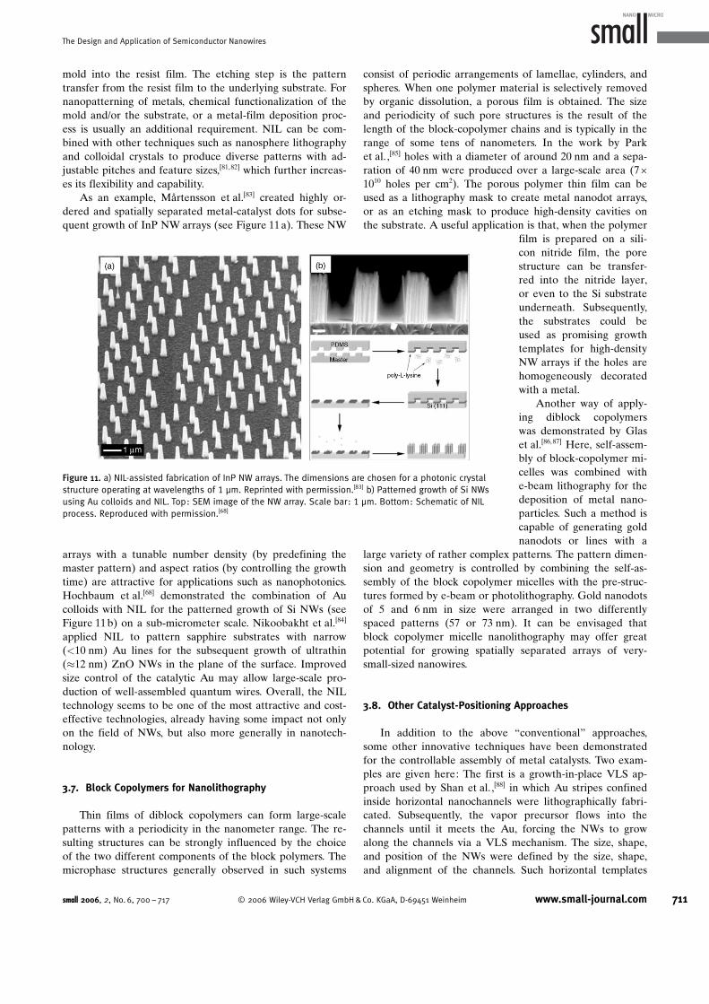
As an example, MMrtensson et al.[83] created highly or-dered and spatially separated metal-catalyst dots for subse-quent growth of InP NW arrays (see Figure 11a). These NW
arrays with a tunable number density (by predefining themaster pattern) and aspect ratios (by controlling the growthtime) are attractive for applications such as nanophotonics.Hochbaum et al.[68] demonstrated the combination of Aucolloids with NIL for the patterned growth of Si NWs (seeFigure 11b) on a sub-micrometer scale. Nikoobakht et al.[84]
applied NIL to pattern sapphire substrates with narrowACHTUNGTRENNUNG(<10 nm) Au lines for the subsequent growth of ultrathinACHTUNGTRENNUNG(�12 nm) ZnO NWs in the plane of the surface. Improvedsize control of the catalytic Au may allow large-scale pro-duction of well-assembled quantum wires. Overall, the NILtechnology seems to be one of the most attractive and cost-effective technologies, already having some impact not onlyon the field of NWs, but also more generally in nanotech-nology.
3.7. Block Copolymers for Nanolithography
Thin films of diblock copolymers can form large-scalepatterns with a periodicity in the nanometer range. The re-sulting structures can be strongly influenced by the choiceof the two different components of the block polymers. Themicrophase structures generally observed in such systems
consist of periodic arrangements of lamellae, cylinders, andspheres. When one polymer material is selectively removedby organic dissolution, a porous film is obtained. The sizeand periodicity of such pore structures is the result of thelength of the block-copolymer chains and is typically in therange of some tens of nanometers. In the work by Parket al. ,[85] holes with a diameter of around 20 nm and a sepa-ration of 40 nm were produced over a large-scale area (7O1010 holes per cm2). The porous polymer thin film can beused as a lithography mask to create metal nanodot arrays,or as an etching mask to produce high-density cavities onthe substrate. A useful application is that, when the polymer
film is prepared on a sili-con nitride film, the porestructure can be transfer-red into the nitride layer,or even to the Si substrateunderneath. Subsequently,the substrates could beused as promising growthtemplates for high-densityNW arrays if the holes arehomogeneously decoratedwith a metal.
Another way of apply-ing diblock copolymerswas demonstrated by Glaset al.[86, 87] Here, self-assem-bly of block-copolymer mi-celles was combined withe-beam lithography for thedeposition of metal nano-particles. Such a method iscapable of generating goldnanodots or lines with a
large variety of rather complex patterns. The pattern dimen-sion and geometry is controlled by combining the self-as-sembly of the block copolymer micelles with the pre-struc-tures formed by e-beam or photolithography. Gold nanodotsof 5 and 6 nm in size were arranged in two differentlyspaced patterns (57 or 73 nm). It can be envisaged thatblock copolymer micelle nanolithography may offer greatpotential for growing spatially separated arrays of very-small-sized nanowires.
3.8. Other Catalyst-Positioning Approaches
In addition to the above “conventional” approaches,some other innovative techniques have been demonstratedfor the controllable assembly of metal catalysts. Two exam-ples are given here: The first is a growth-in-place VLS ap-proach used by Shan et al.,[88] in which Au stripes confinedinside horizontal nanochannels were lithographically fabri-cated. Subsequently, the vapor precursor flows into thechannels until it meets the Au, forcing the NWs to growalong the channels via a VLS mechanism. The size, shape,and position of the NWs were defined by the size, shape,and alignment of the channels. Such horizontal templates
Figure 11. a) NIL-assisted fabrication of InP NW arrays. The dimensions are chosen for a photonic crystalstructure operating at wavelengths of 1 mm. Reprinted with permission.[83] b) Patterned growth of Si NWsusing Au colloids and NIL. Top: SEM image of the NW array. Scale bar: 1 mm. Bottom: Schematic of NILprocess. Reproduced with permission.[68]
small 2006, 2, No. 6, 700 – 717 ( 2006 Wiley-VCH Verlag GmbH&Co. KGaA, D-69451 Weinheim www.small-journal.com 711
The Design and Application of Semiconductor Nanowires

are an integral component of the final devices and providecontacts and interconnects of the NWs without the normal“pick-and-place” or printing steps.
A second example, which can be called “crack lithogra-phy”, was demonstrated by Adelung et al.[89] The processbegins by creating nanoscopic cracks in a brittle thin sacrifi-cial film by inducing mechanical stresses in the film. Onceformed, these cracks can be used as templates for horizontalNW formation by depositing material into the cracks. In thisway, metal NWs with diameters down to 14 nm can easilybe realized. While this approach could in principle be ex-tended to the deposition of horizontal NWs of almost anycomposition, the challenge is the uniformity, alignment, andcrystallinity of the NWs. Nevertheless, the metal NWs creat-ed in this way could be used as catalysts for further conven-tional VLS growth of semiconductor NWs where single-crystalline substrates are used.
4. Patterned Nanowire Arrays by Non-VLS-basedTechniques
While most site-defined NW fabrication techniques in-volve metal-catalyst templates, there are also some interest-ing and reliable approaches to catalyst-free and non-VLS-based growth of NW arrays. Fukui and co-workers haveused a so-called selective-area metalorganic vapor phase ep-itaxy technique to fabricate vertically aligned III–V NWarrays on selectively masked epitaxial substrates (see
Figure 12).[90-92] The process begins with spatially controlledgrowth of an epitaxial layer through an opening in a SiO2
mask (which was predeposited by plasma sputtering). NWswere formed by further growth based on the epitaxial layer.The length, diameter, shape, and position of the NWs werecontrolled by manipulating the growth conditions and maskpatterning.[90] More remarkably, epitaxial core–shell GaAs/InGaAs and InP/InAs NW arrays were also realized by thesequential feeding of metalorganic precursors (Fig-ure 12c).[91,92] Further, by dry etching the core material, theyalso obtained arrays of semiconductor nanotubes that exhib-it reasonably good electrical conductivity (Figure 12d).[92]
In catalyst-free aqueous-phase growth modes, the resultis usually a film of closely packed NWs covering the wholesubstrate surface. However, by applying microcontact print-ing,[61, 93] micromolding,[94] or conventional lithography tech-niques[95] to pattern the substrate surface or a predepositedseed layer, it is also possible to achieve cm2-scale orderedNWs arrays in dots, lines, and a variety of complex struc-tures, as demonstrated recently. Although the patterns arestill on the micrometer scale, the concept can be extendedto nanopatterning when interference photolithography ormodern soft-lithography techniques are utilized.
5. Towards Devices and Functions
The growth mechanisms used in various NW fabricationprocesses are still far from being understood in detail, and
various nanolithographicapproaches are under de-velopment to realize abetter control of the spatialarrangement of the NWs.Nevertheless, investigationon multifunctional applica-tions of semiconductorNWs have already started.Due to their high anisotro-py in structure, such one-dimensional structures aredistinguished from theirbulk counterparts in vari-ous aspects of their proper-ties, as has been demon-strated by theory and nu-merous experiments. It wasshown that NWs mighthave unique size-depend-ent mechanical proper-ties,[96, 97] an increased lumi-nescence efficiency,[98] a re-duced threshold for laseroperation,[9] an enhancedelectromechanical re-sponse,[99] and an enhancedthermoelectric efficiencycompared to conventionalPeltier elements.[100]
Figure 12.Well-ordered NW arrays by selective-area metalorganic vapor phase epitaxy (SA-MOVPE): a) Sche-matic of the fabrication technique, which enables the size-defined growth of NWs, core–shell NWs, as wellas nanotubes of III–V semiconductors; b) an InP NW array; c) GaAs/AlGaAs core–shell NWs; d) InAs nano-tubes after removing the InP core of initial core–shell NWs. Reprinted with permission.[90-92]
712 www.small-journal.com ( 2006 Wiley-VCH Verlag GmbH&Co. KGaA, D-69451 Weinheim small 2006, 2, No. 6, 700 – 717
reviews M. Zacharias et al.
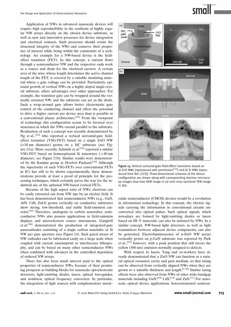
Application of NWs in advanced nanoscale devices willrequire high reproducibility in the synthesis of highly regu-lar NW arrays directly on the chosen device substrate, aswell as new and innovative processes for device integrationand electrical contacts. Such processes should retain thestructural integrity of the NWs and conserve their proper-ties of interest while being within the constraints of a tech-nology. An example for a NW-based device is the field-effect transistor (FET). In this concept, a current flowsthrough a semiconductor NW and the respective ends workas a source and drain for the electrical carriers. A certainarea of the wire, whose length determines the active channellength of the FET, is covered by a suitable insulating mate-rial where a gate voltage can be provided. Particularly, epi-taxial growth of vertical NWs on a highly doped single-crys-tal substrate offers advantages over other approaches: Forexample, the transistor gate can be wrapped around the ver-tically oriented NW, and the substrate can act as the drain.Such a wrap-around gate allows better electrostatic gatecontrol of the conducting channel and offers the potentialto drive a higher current per device area than is possible ina conventional planar architecture.[101] From the viewpointof technology this configuration seems to be favored overstructures in which the NWs extend parallel to the substrate.Realization of such a concept was recently demonstrated byNg et al.,[102] who reported a vertical surround-gate field-effect transistor (VSG-FET) based on a single ZnO NW(�30 nm diameter) grown on a SiC substrate (see Fig-ACHTUNGTRENNUNGure 13a). More recently, Schmidt et al.[103] reported a similarVSG-FET based on homoepitaxial Si nanowires (�40 nmdiameter; see Figure 13b). Similar results were demonstrat-ed by the Kamins group at Hewlett–Packard.[104] Althoughthe superiority of such VSG-FETs over conventional FETsin ICs has still to be shown experimentally, these demon-strations provide at least a proof of principle for the pro-ACHTUNGTRENNUNGcessing techniques, which certainly paves the way for the in-dustrial use of the epitaxial NW-based vertical FETs.
Because of the high aspect ratio of NWs, electrons canbe easily extracted out from NW tips by an electric field. Ithas been demonstrated that semiconductor NWs (e.g., GaN,AlN, CdS, ZnO) grown vertically on conductive substratesshow strong, low-threshold, and stable field-emission cur-rents.[105] Therefore, analogous to carbon nanotubes, semi-conductor NWs also possess applications in field-emissiondisplays and microelectron source instruments. Gangloffet al.[106] demonstrated the production of integrated-gatenanocathodes consisting of a single carbon nanotube or SiNW per gate aperture (see Figure 14). Such gated arrays ofNW cathodes can be fabricated easily on a large scale whencoupled with current nanoimprint or interference lithogra-phy, and can be based on many other semiconductor NWswhen combined with advances in the controlled depositionof ordered NW arrays.
There has also been much interest paid to the opticalproperties of semiconductor NWs, because of their promis-ing prospects as building blocks for nanoscale optoelectronicdetectors, light-emitting diodes, lasers, optical waveguides,and nonlinear optical frequency converters. In particular,the integration of light sources with complementary metal–
oxide semiconductor (CMOS) devices would be a revolutionin information technology. In this concept, the electric sig-nals carrying the information in conventional circuits areconverted into optical pulses. Such optical signals, whichnowadays are formed by light-emitting diodes or lasersbased on III–V materials, can also be initiated by NWs. In asimilar concept, NW-based light detectors, as well as lighttransmitters between adjacent device components, can alsobe generated. Electroluminescence of n-ZnO NW arraysvertically grown on p-GaN substrate was reported by Parket al. ,[107] however, with a peak position that still favors theyellow (560 nm) emission normally assigned to defects.
With respect to lasers, Yang and co-workers have al-ready demonstrated that a ZnO NW can function as a natu-ral optical resonator cavity and gain medium, so that lasingcan be observed from vertically aligned NWs when they aregrown to a suitable thickness and length.[9, 108] Similar lasingeffects were also observed from NWs of other wide-bandgapmaterials including GaN,[109] CdS,[110] and ZnS.[111] For nano-scale optical device applications, heterostructural semicon-
Figure 13. Vertical surround-gate field-effect transistors based ona) ZnO NWs (reproduced with permission[102]) and b) Si NWs (repro-duced from Ref. [103]). Three-dimensional schemes of the deviceconfiguration are shown along with corresponding electron microsco-py images (top-view SEM image in (a) and cross-sectional TEM imagein (b)).
small 2006, 2, No. 6, 700 – 717 ( 2006 Wiley-VCH Verlag GmbH&Co. KGaA, D-69451 Weinheim www.small-journal.com 713
The Design and Application of Semiconductor Nanowires

ductor NWs with modulated compositions might be superiorto NWs of pure composition. Surface states are known tocause some deleterious effects. For example, they can act asrecombination centers for minority carriers, thus degradingthe performance of optoelectronic devices of NWs.[112] Suchnegative consequences can be avoided by passivating thenanowire surface immediately after core definition, formingcore–shell nanowires. A shell dielectric could be used toform a high-quality optical cavity around a small-core NWacting as the gain medium. More novel material combina-tions involving, for example, hetero- or homoepitaxial semi-conductors (e.g., Si–Ge,[113] ZnO–GaN,[114] p–n GaN[115]), fer-roelectric and magnetic materials (e.g., MgO–PZT,[116]
MgO–Fe3O4[117]) open the door to a wide variety of func-
tionalities in such core–shell NWs.Semiconductor NWs of sufficiently small diameter (i.e.,
close to the corresponding exciton Bohr radius) should ex-hibit quantum-confinement-related effects, which, for exam-ple, strongly influence the optical properties. This has al-ready been demonstrated for NWs of III–V semiconduc-tors,[118] ZnO,[119,120] as well as for silicon.[121,122] Silicon is themost important microelectronic material. However, it haspoor optical emission properties due to its indirect bandgaptransitions. It is expected that Si and Si/Ge nanostructuresmay have a much higher luminescence efficiency than bulkSi, because the band structure of a NW can be modified in away that the radiative recombination probability is signifi-cantly enhanced. Consequently, new (group IV) optoelec-tronic devices might be realized. This could allow the com-bination of electrical and optical functions on the same Si-
based chip. It was also re-ported that quantum ef-fects could reduce the heatconductance, which couldbe used for new coolingconcepts based on NWs.[123]
For electric-carrier trans-port in NWs, phenomenaof interest include: 1) theaforementioned quantumconfinement, 2) ballisticcarrier transport, whichcorresponds to a high mo-bility, and 3) tunneling ofelectrons between NWsand corresponding hetero-structures (“Coulombblockade”). At themoment it is to early tojudge in which way theseproperties might have ause in future technology.
One possible applica-tion of NWs lies in thefield of biotechnology; dif-ferent functional conceptsare under discussion. NWnanosensors have beensuggested for highly sensi-
tive and selective detection of biological and chemical spe-cies.[124] This approach might even offer the possibility todetect the selected attachment of single molecules. Al-though most of the discussed concepts for the use of NWsin the field of human medicine are still speculative, a fastdevelopment of applications in various fields is expectedwithin the next decade. There have been a number of na-tional and multinational initiatives for nanotechnologylaunched during the last couple of years, which should serveto advance these concepts. Parallel to this scientific andtechnological evolution, one should also keep in mind thepotential environmental risks associated with nanowires, al-though this risk should be minimal for semiconductor nano-wires embedded in circuits.
6. Summary and Outlook
With the remarkable progress in research on the synthe-sis of semiconductor nanowires over recent years, one-di-mensional growth with superior control in structure, dimen-sion, and spatial alignment becomes more and more impor-tant. In this Review, typical growth approaches for semicon-ductor NWs were discussed, which fall into two main cate-gories: vapor-phase and wet-chemical approaches. Wefocused on the vapor–liquid–solid growth mode because itprovides a technical opportunity for in situ position, defini-tion, and size control of the nanowires. Nearly all existingtechnologies, from conventional photolithography to state-of-the-art nanoimprint lithography, have been employed for
Figure 14. Gated arrays of individual 1D nanostructures for application as emitter arrays. a) An array of inte-grated gate Si NW cathodes; b) SEM image of an integrated carbon nanotube cathode showing the gateelectrode, insulator, and emitter electrode; c) schematics of a single nanowire/nanotube emitter. Repro-duced with permission.[106]
714 www.small-journal.com ( 2006 Wiley-VCH Verlag GmbH&Co. KGaA, D-69451 Weinheim small 2006, 2, No. 6, 700 – 717
reviews M. Zacharias et al.
the spatial control of the positioning of nanowires. Thetrend for better control of nanowire growth is accompaniedby progress in templating techniques.
Nevertheless, for the nanopatterned growth of semicon-ductor NWs on a macroscopic scale, an improvement of cur-rent techniques is still needed and/or an innovative technol-ogy should be developed. Such new techniques should givehigh processing resolution and efficiency, and allow epitaxialNW growth with good crystallinity. This is highly desirableto future nanomanufacturing and applications, and is in par-ticular an essential step towards in situ integration of well-aligned nanowires into devices with existing technologies,for example, vertical transistors, electron field-emitterarrays, and biosensor arrays.
This Review also covered some concerns and recentdemonstrations for using semiconductor NW as electronicand photonic devices. Due to their low dimensionality andsemiconducting nature, the NWs may exhibit unique elec-tronic and optical properties relative to bulk semiconduc-tors. In many cases, the detailed mechanisms behind theirbehavior are not yet understood in detail. Nevertheless, in-dependent of whether these properties are desirable or not,they should be well understood when using semiconductorNWs. There is not doubt that NWs will create countless newopportunities in research and hopefully also in technology.
Acknowledgements
The authors would like to thank the DFG for funding part ofthe research presented here (contract ZA 191/17-1). Discus-sions on the subject of semiconductor nanowires and tem-plating methods with U. Gçsele, K. Nielsch, and many othercolleagues are gratefully acknowledged.
[1] S. Iijima, Nature 1991, 354, 56.[2] Whisker Technology (Ed.: A. P. Levitt), New York, USA Wiley-In-
terscience, 1970.[3] For example, see the following reviews and references therein:
a) Y. Xia, P. Yang, Y. Sun, Y. Wu, B. Mayers, B. Gates, Y. Yin, F.Kim, H. Yan, Adv. Mater. 2003, 15, 353; b) C. N. R. Rao, F. L.Deepak, G. Gundiah, A. Govindaraj, Prog. Solid State Chem.2003, 31, 5.
[4] R. S. Wagner, W. C. Ellis, Trans. Metall. Soc. AIME 1965, 233,1053.
[5] Y. Wu, P. Yang, J. Am. Chem. Soc. 2001, 123, 3165.[6] F. M. Ross, J. Tersoff, M. C. Reuter, Phys. Rev. Lett. 2005, 95,
146104.[7] K. Haraguchi, T. Katsuyama, K. Hiruma, K. Ogawa, Appl. Phys.
Lett. 1992, 60, 745.[8] A. M. Morales, C. M. Lieber, Science 1998, 279, 208.[9] M. H. Huang, S. Mao, H. Feick, H. Yan, Y. Wu, H. Kind, E. Weber,
R. Russo, P. Yang, Science 2001, 292, 1897.[10] H. J. Fan, W. Lee, R. Scholz, A. Dadgar, A. Krost, K. Nielsch, M.
Zacharias, Nanotechnology 2005, 16, 913.[11] L. Samuelson, Mater. Today 2003, 6, 22.[12] L. Schubert, P. Werner, N. D. Zakharov, G. Gerth, F. M. Kolb, L.
Long, U. Gçsele, T. Y. Tan, Appl. Phys. Lett. 2004, 84, 4968.[13] J. B. Hannon, S. Kodambaka, F. M. Ross, R. M. Tromp, Nature
2006, 440, 69.[14] R. S. Wagner, W. C. Ellis, Appl. Phys. Lett. 1964, 4, 89.
[15] E. I. Givargizov, A. A. Chernov, J. Cryst. Growth 1975, 31, 20.[16] G. A. Bootsma, H. J. Gassen, J. Cryst. Growth 1971, 10, 223.[17] J. Westwater, D. P. Gosain, S. Tomiya, S. Usui, H. Ruda, J. Vac.
Sci. Technol. B 1997, 15, 554.[18] J. L. Liu, S. J. Cai, G. L. Jin, S. G. Thomas, K. L. Wang, J. Cryst.
Growth 1999, 200, 106.[19] X. Duan, C. M. Lieber, Adv. Mater. 2000, 12, 298.[20] M. K. Sunkara, S. Sharma, R. Miranda, G. Lian, E. C. Dickey,
Appl. Phys. Lett. 2001, 79, 1546.[21] B. J. Ohlsson, M. T. Bjçrk, M. H. Magnusson, K. Deppert, L. Sa-
muelson, L. R. Wallenberg, Appl. Phys. Lett. 2001, 79, 3335.[22] F. M. Kolb, H. Hofmeister, R. Scholz, M. Zacharias, U. Gçsele,
D. D. Ma, S. T. Lee, J. Electrochem. Soc. 2004, 151, G472.[23] M. K. Sunkara, S. Sharma, R. Miranda, G. Lian, E. C. Dickey,
Appl. Phys. Lett. 2001, 79, 1546.[24] T. I. Kamins, R. S. Williams, T. Hesjedal, J. S. Harris, Physica E
2002, 13, 995.[25] M. S. Gudiksen, L. J. Lauhon, J. Wang, D. C. Smith, C. M. Lieber,
Nature 2002, 415, 617.[26] B. J. Ohlsson, M. T. Bjçrk, A. I. Persson, C. Thelander, L. R. Wal-
lenberg, M. H. Magnusson, K. Deppert, L. Samuelson, PhysicaE 2002, 13, 1126.
[27] Y. Wu, R. Fan, P. Yang, Nano Lett. 2002, 2, 83.[28] G. KMstner, U. Gçsele, Appl. Phys. Lett. 2003, 82, 3209.[29] G. KMstner, U. Gçsele, Philos. Mag. 2004, 84, 3803.[30] M. T. Bjçrk, B. J. Ohlsson, T. Sass, A. I. Persson, C. Thelander,
M. H. Magnusson, K. Deppert, L. R. Wallenberg, L. Samuelson,Nano Lett. 2002, 2, 87.
[31] Y. Wu, Y. Cui, L. Huynh, C. J. Barrelet, D. C. Bell, C. M. Lieber,Nano Lett. 2004, 4, 433.
[32] V. Schmidt, S. Senz, U. Gçsele, Nano Lett. 2005, 5, 931.[33] T. Kuykendall, P. J. Pauzauskie, Y. Zhang, J. Goldberger, D. Sir-
buly, J. Denlinger, P. Yang, Nat. Mater. 2004, 3,524.[34] Z. R. Dai, Z. W. Pan, Z. L. Wang, Adv. Funct. Mater. 2003, 13, 9.[35] H. Z. Zhang, Y. C. Kong, Y. Z. Wang, X. Du, Z. G. Bai, J. J. Wang,
D. P. Yu, Y. Ding, Q. L. Huang, S. Q. Feng, Solid State Commun.1999, 109, 677.
[36] H. J. Fan, F. Bertram, A. Dadgar, J. Christen, A. Krost, M. Zacha-rias, Nanotechnology 2004, 15, 1401.
[37] S. M. Zhou, Y. S. Feng, L. D. Zhang, Chem. Phys. Lett. 2003,369, 610.
[38] Z. L. Wang, X. Y. Kong, Y. Ding, P. Gao, W. L. Hughes, R. Yang, Y.Zhang, Adv. Funct. Mater. 2004, 14, 943.
[39] a) C. R. Martin, Science 1994, 266, 1961; b) C. R. Martin,Chem. Mater. 1996, 8, 1739.
[40] J. C. Hulteen, C. R. Martin, in Nanoparticles and NanostructuredFilms: Preparation, Characterization and Applications (Ed.: J. H.Fendler), Wiley-VCH, Weinheim, 1998.
[41] S. Shingubara, O. Okino, Y. Sayama, H. Sakaue, T. Takahagi,Solid State Electron. 1999, 43, 1143.
[42] W. Lee, R. Scholz, K. Nielsch, U. Gçsele, Angew. Chem. 2005,117, 6204; Angew. Chem. Int. Ed. 2005, 44, 6050.
[43] D. Routkevitch, T. Bigioni, M. Moskovits, J. M. Xu, J. Phys.Chem. 1996, 100, 14037.
[44] D. Xu, D. Chen, Y. Xu, X. Shi, G. Guo, L. Gui, Y. Tang, Pure Appl.Chem. 2000, 72, 127.
[45] D. Xu, Y. Xu, D. Chen, G. Guo, L. Gui, Y. Tang, Adv. Mater. 2000,12, 520.
[46] J. Choi, K. Nielsch, M. Reiche, R. B. Wehrspohn, U. Gçsele, J.Vac. Sci. Technol. A 2003, 21, 763.
[47] J. Choi, G. Sauer, K. Nielsch, R. B. Wehrspohn, U. Gçsele,Chem. Mater. 2003, 15, 776.
[48] M. P. Zach, K. H. Ng, R. M. Penner, Science 2000, 290, 2120.[49] E. C. Walter, B. J. Murray, F. Favier, R. M. Penner, Adv. Mater.
2003, 15, 396.[50] E. J. Menke, Q. Li, R. M. Penner, Nano Lett. 2004, 4, 2009.[51] M. Geissler, Y. Xia, Adv. Mater. 2004, 16, 1249.
small 2006, 2, No. 6, 700 – 717 ( 2006 Wiley-VCH Verlag GmbH&Co. KGaA, D-69451 Weinheim www.small-journal.com 715
The Design and Application of Semiconductor Nanowires
[52] Q. Li, R. M. Penner, Nano Lett. 2005, 5, 1720.[53] C. B. Murray, D. J. Norris, M. G. Bawendi, J. Am. Chem. Soc.
1993, 115, 8706.[54] L. Manna, E. C. Scher, P. Alivisatos, J. Am. Chem. Soc. 2000,
122, 12700.[55] J. D. Holmes, K. P. Johnston, R. C. Doty, B. A. Korgel, Science
2000, 287, 1471.[56] T. Hanrath, B. A. Korgel, J. Am. Chem. Soc. 2002, 124, 1424.[57] L. Vayssieres, K. Keis, S. E. Lindquist, A. Hagfeldt, J. Phys.
Chem. B 2001, 105, 3350.[58] K. Govender, D. S. Boyle, P. O’Brien, D. Binks, D. West, D. Cole-
man, Adv. Mater. 2002, 14, 1221.[59] J.-H. Choy, E.-S. Jang, J.-H. Won, J.-H. Chung, D.-J. Jang, Y.-W.
Kim, Adv. Mater. 2003, 15, 1911.[60] L. E. Greene, M. Law, J. Goldberger, F. Kim, J. C. Johnson, Y.
Zhang, R. J. Saykally, P. Yang, Angew. Chem. 2003, 115, 3139;Angew. Chem. Int. Ed. 2003, 42, 3031.
[61] See review and references in: T. L. Sounart, J. Liu, J. A. Voigt,J. W. P. Hsu, E. D. Spoerke, Z. Tian, Y. B. Jiang, Adv. Funct.Mater. 2006, 16, 335.
[62] E. C. Greyson, Y. Babayan, T. W. Odom, Adv. Mater. 2004, 16,1348.
[63] H. T. Ng, J. Han, T. Yamada, P. Nguyen, Y. P. Chen, M. Meyyap-pan, Nano Lett. 2004, 4, 1247.
[64] T. Martensson, M. Borgstrom, W. Seifert, B. J. Ohlsson, L. Sa-muelson, Nanotechnology 2003, 14, 1255.
[65] L. E. Jensen, M. T. Bjçrk, S. Jeppesen, A. I. Persson, B. J. Ohls-son, L. Samuelson, Nano Lett. 2004, 4, 1961.
[66] B. J. Ohlsson, M. T. Bjçrk, M. H. Magnusson, K. Deppert, L. Sa-muelson, L. R. Wallenberg, Appl. Phys. Lett. 2001, 79, 3335.
[67] Y. Cui, L. J. Lauhon, M. S. Gudiksen, J. Wang, C. M. Lieber, Appl.Phys. Lett. 2001, 78, 2214.
[68] A. I. Hochbaum, R. Fan, R. He, P. Yang, Nano Lett. 2005, 5,457.
[69] A. Korsiorek, W. Kandulski, P. Churdziski, K. Kempa, M. Giersig,Nanotechnology 2004, 15, 1359.
[70] K. Kempa, B. Kimball, J. Rybczynski, Z. P. Huang, P. F. Wu, D.Steeves, M. Sennett, M. Giersig, D. V. G. L. N. Rao, D. L. Carna-han, D. Z. Wang, J. Y. Lao, W. Z. Li, Z. F. Ren, Nano Lett. 2003,3, 13.
[71] J. Rybczynski, D. Banerjee, A. Kosiorek, M. Giersig, Z. F. Ren,Nano Lett. 2004, 4, 2037.
[72] X. Wang, C. J. Summers, Z. L. Wang, Nano Lett. 2004, 4, 423.[73] H. J. Fan, B. Fuhrmann, R. Scholz, F. Syrowatka, A. Dadgar, A.
Krost, M. Zacharias, J. Cryst. Growth 2006, 287, 34.[74] B. Fuhrmann, H. S. Leipner, H.-R. Hçche, L. Schubert, P.
Werner, U. Gçsele, Nano Lett. 2005, 5, 2524.[75] H. Matsuda, F. Fukuda, Science 1995, 268, 1466.[76] Z. H. Wu, X. Y. Mei, D. Kim, M. Blumin, H. E. Ruda, Appl. Phys.
Lett. 2002, 81, 5177.[77] H. Chik, J. Liang, S. G. Cloutier, N. Kouklin, J. M. Xu, Appl. Phys.
Lett. 2004, 84, 3376.[78] W. Lee, M. Alexe, K. Nielsch, U. Gçsele, Chem. Mater. 2005,
17, 3325.[79] S. Y. Chou, P. R. Krauss, P. J. Renstrom, Science 1996, 272, 85.[80] B. D. Gates, Q. Xu, M. Stewart, D. Ryan, C. G. Willson, G. M.
Whitesides, Chem. Rev. 2005, 105, 1171.[81] J. Yao, X. Yan, G. Lu, K. Zhang, X. Chen, L. Jiang, B. Yang, Adv.
Mater. 2004, 16, 81.[82] P. Maury, M. Peter, V. Mahalingam, D. N. Reinhoudt, J. Husk-
ens, Adv. Funct. Mater. 2005, 15, 451.[83] T. MPrtensson, P. Carlberg, M. Borgstro, L. Montelius, W. Sei-
fert, L. Samuelson, Nano Lett. 2004, 4, 699.[84] B. Nikoobakht, C. A. Michaels, S. J. Stranicka, M. D. Vaudin,
Appl. Phys. Lett. 2004, 85, 3244.[85] M. Park, C. Harrison, P. M. Chaikin, R. A. Register, D. H. Adam-
son, Science 1997, 276, 1401.
[86] R. Glas, M. Mçller, J. P. Spatz, Nanotechnology 2003, 14,1153.
[87] R. Roman, M. Arnold, E. A. Calalcanti-Adam, J. BlQmmel, C. Ha-ferkemper, C. Dodd, J. P. Spatz, New J. Phys. 2004, 6, 101.
[88] Y. Shan, A. K. Kalkan, C.-Y. Peng, S. J. Fonash, Nano Lett. 2004,4, 2085.
[89] R. Adelung, O. C. Aktas, J. Franc, A. Biswas, R. Kunz, M. Elbah-ri, J. Kanzow, U. Schurmann, F. Faupel, Nat. Mater. 2004, 3,375.
[90] P. Mohan, J. Motohisa, T. Fukui, Nanotechnology 2005, 16,2903.
[91] J. Noborisaka, J. Motohisa, S. Hara, T. Fukui, Appl. Phys. Lett.2005, 87, 093109.
[92] P. Mohan, J. Motohisa, T. Fukui, Appl. Phys. Lett. 2006, 88,013110.
[93] J. W. P. Hsu, Z. R. Tian, N. C. Simmons, C. M. Matzke, J. A. Voigt,J. Liu, Nano Lett. 2005, 5, 83.
[94] S. J. Kwon, J. H. Park, J. G. Park, Appl. Phys. Lett. 2005, 87,133112.
[95] J. F. Conley, Jr., L. Stecker, Y. Ono, Nanotechnology 2005, 16,292.
[96] G. Rubio-Bollinger, S. R. Bahn, N. Agrait, K. W. Jacobsen, S.Vieira, Phys. Rev. Lett. 2001, 87, 026101.
[97] S. Cuenot, C. Fretigny, S. D. Champagne, B. Nysten, Phys. Rev.B 2004, 69, 65410.
[98] T. K. Sham, S. J. Naftel, P. S. G. Kim, R. Sammynaiken, Y. H.Tang, I. Coulthard, A. Moewes, J. W. Freeland, Y. F. Hu, S. T. Lee,Phys. Rev. B 2004, 70, 045313.
[99] M. H. Zhao, Z. L. Wang, S. X. Mao, Nano Lett. 2004, 4, 587.[100] Y. M. Lin, X. Sun, M. S. Dresselhaus, Phys. Rev. B 2000, 62,
4610.[101] J. Wang, E. Polizzi, M. Lundstrom, J. Appl. Phys. 2004, 96,
2192.[102] H. T. Ng, J. Han, T. Yamada, P. Nguyen, Y. P. Chen, M. Meyyap-
pan, Nano Lett. 2004, 4, 1247.[103] V. Schmidt, H. Riel, S. Senz, S. Karg, W. Riess, U. Gçsele, Small
2006, 2, 85.[104] Q. Tang, T. I. Kamins, X. Liu, D. E. Grupp, J. S. Harris, Electro-
chem. Solid-State Lett. 2005, 8, G204.[105] a) Y. K. Tseng, C. J. Huang, H. M. Cheng, I. N. Lin, K. S. Liu, I. C.
Chen, Adv. Funct. Mater. 2003, 13, 811; b) Y. W. Zhu, H. Z.Zhang, X. C. Sun, S. Q. Feng, J. Xu, Q. Zhao, B. Xiang, R. M.Wang, D. P. Yu, Appl. Phys. Lett. 2003, 83, 144; c) B. D. Liu, Y.Bando, C. C. Tang, F. F. Xu, D. Golberg, J. Phys. Chem. B 2005,109, 21521; d) Q. Tang, X. H. Chen, T. Li, A. W. Zhao, Q. T.Qian, D. P. Yu, W. C. Yu, Chem. Lett. 2004, 33, 1088; e) S. Q. Li,Y. X. Liang, T. H. Wang, Appl. Phys. Lett. 2005, 87, 143104;f) S. C. Shi, C. F. Chen, S. Chattopadhyay, K. H. Chen, L. C.Chen, Appl. Phys. Lett. 2005, 87, 073109.
[106] L. Gangloff, E. Minoux, K. B. K. Teo, P. Vincent, V. T. Semet, V. T.Binh, M. H. Yang, I. Y. Y. Bu, R. G. Lacerda, G. Pirio, J. P. Schnell,D. Pribat, D. G. Hasko, G. A. J. Amaratunga, W. I. Milne, P. Le-gagneux, Nano Lett. 2004, 4, 1575.
[107] W. I. Park, G. C. Yi, Adv. Mater. 2004, 16, 87.[108] J. C. Johnson, H. Yan, R. D. Schaller, L. H. Haber, R. J. Saykally,
P. Yang, J. Phys. Chem. B 2001, 105, 11387.[109] J. C. Johnson, H.-J. Choi, K. P. Knutsen, R. D. Schaller, P. Yang,
R. J. Saykally, Nat. Mater. 2002, 1, 106.[110] X. Duan, H. Huang, R. Agrawal, C. M. Lieber, Nature 2003, 421,
241.[111] J. X. Ding, J. A. Zapien, W. W. Chen, Y. Lifshitz, S. T. Lee, X. M.
Meng, Appl. Phys. Lett. 2004, 85, 2361.[112] L. J. Lauhon, M. S. Gudiksen, C. M. Lieber, Philos. Trans. R. Soc.
London Ser. A 2004, 362, 1247.[113] L. J. Lauhon, M. S. Gudiksen, D. Wang, C. M. Lieber, Nature
2002, 420, 57.
716 www.small-journal.com ( 2006 Wiley-VCH Verlag GmbH&Co. KGaA, D-69451 Weinheim small 2006, 2, No. 6, 700 – 717
reviews M. Zacharias et al.

[114] S. J. An, W. I. Park, G.-C. Yi, Y.-J. Kim, H.-B. Kang, M. Kim, Appl.Phys. Lett. 2004, 84, 3612.
[115] F. Qian, Y. Li, S. Gradec, D. Wang, C. J. Barrelet, C. M. Lieber,Nano Lett. 2004, 4, 1975.
[116] S. Han, C. Li, Z. Liu, B. Lei, D. Zhang, W. Jin, X. Liu, T. Tang, C.Zhou, Nano Lett. 2004, 4, 1241.
[117] D. Zhang, Z. Liu, S. Han, C. Li, B. Lei, M. P. Stewart, J. M. Tour,C. Zhou, Nano Lett. 2004, 4, 2151.
[118] S. Bhunia, T. Kawamura, Y. Watanabe, S. Fujikawa, K. Tokushi-ma, Appl. Phys. Lett. 2003, 83, 3371.
[119] W. I. Park, G.-C. Yi, M. Kim, S. J. Pennycook, Adv. Mater. 2003,15, 526.
[120] X. Wang, Y. Ding, C. J. Summers, Z. L. Wang, J. Phys. Chem. B2004, 108, 8773.
[121] D. D. D. Ma, C. S. Lee, F. C. K. Au, S. Y. Tong, S. T. Lee, Science2003, 299, 1874.
[122] X. Y. Zhao, C. M. Wei, L. Yang, M. Y. Chou, Phys. Rev. Lett. 2004,92, 236805.
[123] G. Chen, M. S. Dresselhaus, G. Dresselhaus, J. P. Fleurial, T.Caillat, Int. Mater. Rev. 2003, 48, 45.
[124] Y. Cui, Q. Wei, H. Park, C. M. Lieber, Science 2001, 293, 1289.
Received: December 8, 2005Revised: March 3, 2006
small 2006, 2, No. 6, 700 – 717 ( 2006 Wiley-VCH Verlag GmbH&Co. KGaA, D-69451 Weinheim www.small-journal.com 717
The Design and Application of Semiconductor Nanowires


![Nanoparticle-doped electrospun fiber random lasers with ... · [2,6,8,10]. Organic crystals [16,17] and epitaxial nanowires [18], biopolymers [19,20], as well as conjugated polymers](https://img.dokumen.tips/doc/110x75/600d3d88f8e5ef616721ea08/nanoparticle-doped-electrospun-fiber-random-lasers-with-26810-organic.jpg)

![119 Nanowires 4. Nanowires - UFAMhome.ufam.edu.br/berti/nanomateriais/Nanowires.pdf · 119 Nanowires 4. Nanowires ... written about carbon nanotubes [4.57–59], which can be](https://img.dokumen.tips/doc/110x75/5abfd11e7f8b9a5d718eba2b/119-nanowires-4-nanowires-nanowires-4-nanowires-written-about-carbon-nanotubes.jpg)