Embed Size (px)
Citation preview
Role of Planar Defects in Compound Semiconductor Crystals: From Growth of Nanomasts & Nanosails to Processing Light Emission in DualBeam FIB/SEM.
W.MoberlyChan*, J. Tringe*, I.Shalish**, & V.Narayanamurti** *Lawrence Livermore Natl. Labs., CMLS, Livermore, CA. **Harvard University, Cambridge, MA.
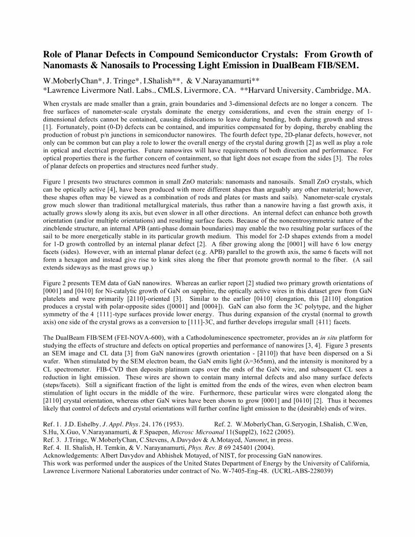
When crystals are made smaller than a grain, grain boundaries and 3-dimensional defects are no longer a concern. The free surfaces of nanometer-scale crystals dominate the energy considerations, and even the strain energy of 1-dimensional defects cannot be contained, causing dislocations to leave during bending, both during growth and stress [1]. Fortunately, point (0-D) defects can be contained, and impurities compensated for by doping, thereby enabling the production of robust p/n junctions in semiconductor nanowires. The fourth defect type, 2D-planar defects, however, not only can be common but can play a role to lower the overall energy of the crystal during growth [2] as well as play a role in optical and electrical properties. Future nanowires will have requirements of both direction and performance. For optical properties there is the further concern of containment, so that light does not escape from the sides [3]. The roles of planar defects on properties and structures need further study. Figure 1 presents two structures common in small ZnO materials: nanomasts and nanosails. Small ZnO crystals, which can be optically active [4], have been produced with more different shapes than arguably any other material; however, these shapes often may be viewed as a combination of rods and plates (or masts and sails). Nanometer-scale crystals grow much slower than traditional metallurgical materials, thus rather than a nanowire having a fast growth axis, it actually grows slowly along its axis, but even slower in all other directions. An internal defect can enhance both growth orientation (and/or multiple orientations) and resulting surface facets. Because of the noncentrosymmetric nature of the zincblende structure, an internal APB (anti-phase domain boundaries) may enable the two resulting polar surfaces of the sail to be more energetically stable in its particular growth medium. This model for 2-D shapes extends from a model for 1-D growth controlled by an internal planar defect [2]. A fiber growing along the [0001] will have 6 low energy facets (sides). However, with an internal planar defect (e.g. APB) parallel to the growth axis, the same 6 facets will not form a hexagon and instead give rise to kink sites along the fiber that promote growth normal to the fiber. (A sail extends sideways as the mast grows up.) Figure 2 presents TEM data of GaN nanowires. Whereas an earlier report [2] studied two primary growth orientations of [0001] and [0110] for Ni-catalytic growth of GaN on sapphire, the optically active wires in this dataset grew from GaN platelets and were primarily [2110]-oriented [3]. Similar to the earlier [0110] elongation, this [2110] elongation produces a crystal with polar-opposite sides ([0001] and [0001]). GaN can also form the 3C polytype, and the higher symmetry of the 4 {111}-type surfaces provide lower energy. Thus during expansion of the crystal (normal to growth axis) one side of the crystal grows as a conversion to [111]-3C, and further develops irregular small {111} facets. The DualBeam FIB/SEM (FEI-NOVA-600), with a Cathodoluminescence spectrometer, provides an in situ platform for studying the effects of structure and defects on optical properties and performance of nanowires [3, 4]. Figure 3 presents an SEM image and CL data [3] from GaN nanowires (growth orientation - [2110]) that have been dispersed on a Si wafer. When stimulated by the SEM electron beam, the GaN emits light (λ=365nm), and the intensity is monitored by a CL spectrometer. FIB-CVD then deposits platinum caps over the ends of the GaN wire, and subsequent CL sees a reduction in light emission. These wires are shown to contain many internal defects and also many surface defects (steps/facets). Still a significant fraction of the light is emitted from the ends of the wires, even when electron beam stimulation of light occurs in the middle of the wire. Furthermore, these particular wires were elongated along the [2110] crystal orientation, whereas other GaN wires have been shown to grow [0001] and [0110] [2]. Thus it becomes likely that control of defects and crystal orientations will further confine light emission to the (desirable) ends of wires. Ref. 1. J.D. Eshelby, J. Appl. Phys. 24, 176 (1953). Ref. 2. W.MoberlyChan, G.Seryogin, I.Shalish, C.Wen, S.Hu, X.Guo, V.Narayanamurti, & F.Spaepen, Microsc Microanal 11(Suppl2), 1622 (2005). Ref. 3. J.Tringe, W.MoberlyChan, C.Stevens, A.Davydov & A.Motayed, Nanonet, in press. Ref. 4. II. Shalish, H. Temkin, & V. Narayanamurti, Phys. Rev. B 69 245401 (2004). Acknowledgements: Albert Davydov and Abhishek Motayed, of NIST, for processing GaN nanowires. This work was performed under the auspices of the United States Department of Energy by the University of California, Lawrence Livermore National Laboratories under contract of No. W-7405-Eng-48. (UCRL-ABS-228039)

FIG. 1. SEM & TEM of ZnO nanomasts & nanosails. 2H-ZnO can grow as a rod, but internal planar defect can promote sideways sail growth. FIG. 2. TEM of GaN-[2110]-oriented nanowire: faults more readily imaged not-normal to wire axis. Non-centrosymmetric structure of GaN encourages β-3C and α-2H growth on opposite sides of wire [2]. FIG. 3. DualBeam FIB/SEM is used to excite light emission (measured with CL), and covering ends of wire with caps of FIB-CVD-Pt can block light. (Defects may affect light leakage from sides.)


![Strain and the optoelectronic properties of non-planar ... · D crystalline soft materials that acquire topological defects while conforming to non-planar shapes [12-15], the materials](https://img.dokumen.tips/doc/110x75/5b82c1247f8b9a934f8bb20e/strain-and-the-optoelectronic-properties-of-non-planar-d-crystalline-soft.jpg)